Embed Size (px)
Citation preview
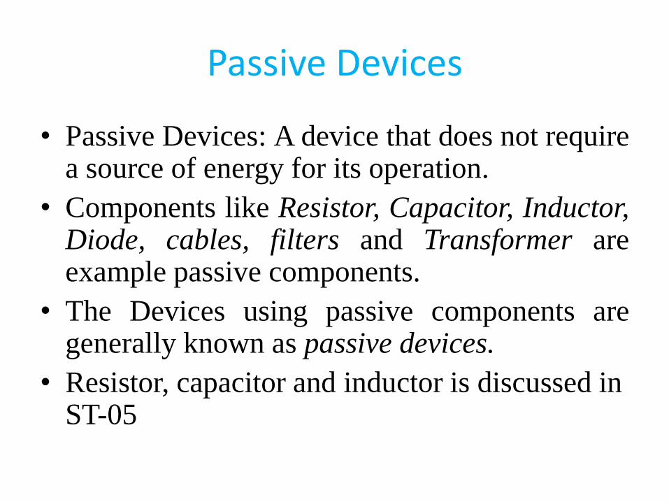
Passive Devices
• Passive Devices: A device that does not require a source of energy for its operation.
• Components like Resistor, Capacitor, Inductor, Diode, cables, filters and Transformer are example passive components.
• The Devices using passive components are generally known as passive devices.
• Resistor, capacitor and inductor is discussed in ST-05
Semiconductor
• Semiconductor: The elements which can act as both conductor as well as insulator depending on the condition is called semiconductor. Eg – Silicon, Germanium.
• It is classified as intrinsic & Extrinsic Semiconductor.
• Intrinsic Semiconductor: A Semiconductor material in its pure form is called Intrinsic Semiconductor. Eg – pure Silicon or Pure Germanium.
• Extrinsic Semiconductor: When some impurity atoms are added to Intrinsic Semiconductor, Extrinsic Semiconductor is formed. Eg – Silicon doped with phosphorus. It is classified into n type & P type.
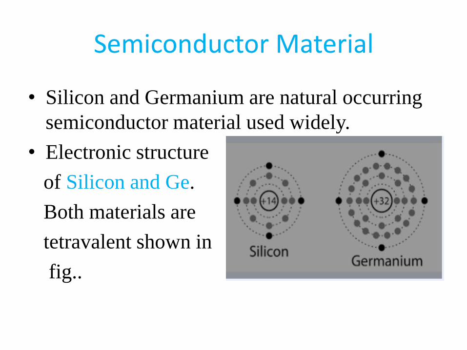
Semiconductor Material
• Silicon and Germanium are natural occurring
semiconductor material used widely.
• Electronic structure
of Silicon and Ge.
Both materials are
tetravalent shown in
fig..
N and P type semiconductor
• N type extrinsic semiconductor: When
pentavalent impurities like Phosphorus, As, Sb
is added to a pure semiconductor, n type
semiconductor is formed.
• P type extrinsic semiconductor: When a
trivalent impurity like Boron, Gallium, Indium
is added to a pure semiconductor, P type
semiconductor is formed.
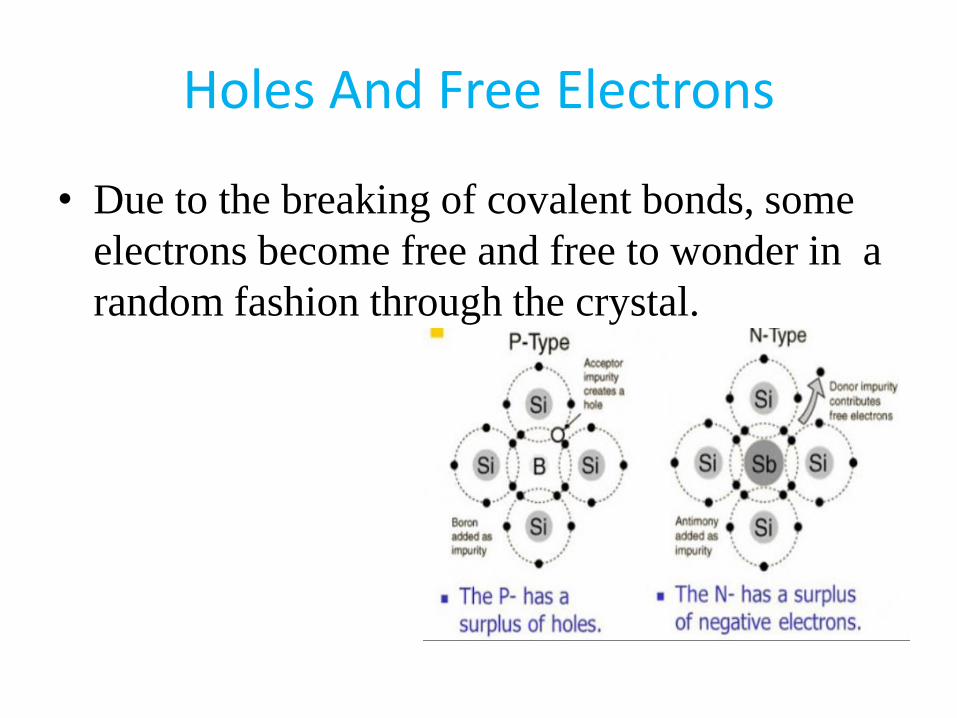
Holes And Free Electrons
• Due to the breaking of covalent bonds, some
electrons become free and free to wonder in a
random fashion through the crystal.
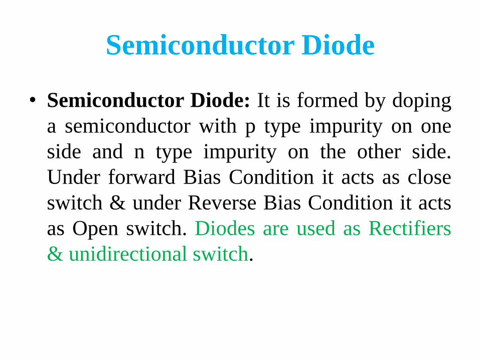
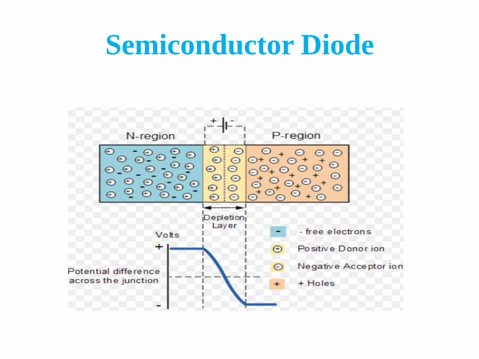
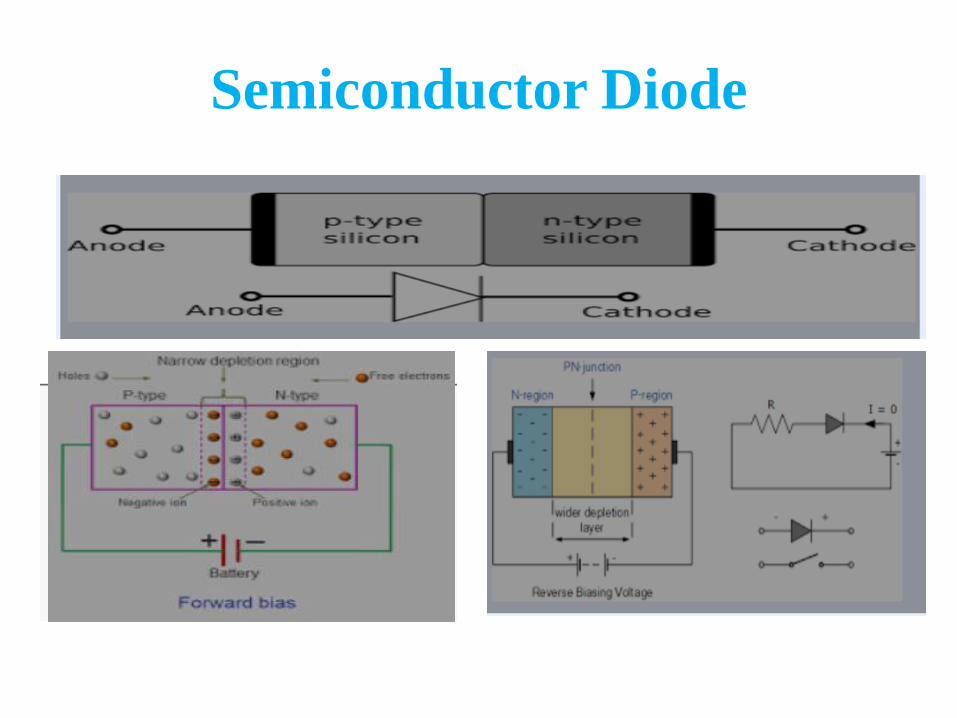
Semiconductor Diode
• Semiconductor Diode: It is formed by doping
a semiconductor with p type impurity on one
side and n type impurity on the other side.
Under forward Bias Condition it acts as close
switch & under Reverse Bias Condition it acts
as Open switch. Diodes are used as Rectifiers
& unidirectional switch.
Semiconductor Diode
Semiconductor Diode
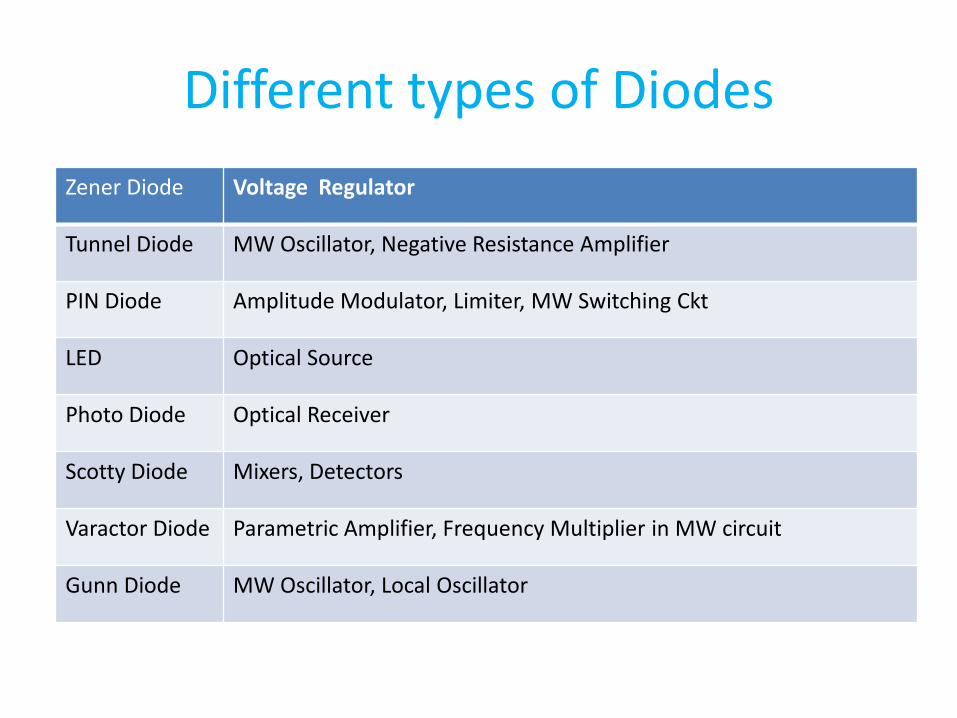
Different types of Diodes
Zener Diode Voltage Regulator
Tunnel Diode MW Oscillator, Negative Resistance Amplifier
PIN Diode Amplitude Modulator, Limiter, MW Switching Ckt
LED Optical Source
Photo Diode Optical Receiver
Scotty Diode Mixers, Detectors
Varactor Diode Parametric Amplifier, Frequency Multiplier in MW circuit
Gunn Diode MW Oscillator, Local Oscillator
Special types of diodes
• There are some special types of diodes which
perform functions like Amplification,
Oscillation, Frequency Multiplication etc. This
is done by varying doping levels in intrinsic
semiconductor or using both Intrinsic &
Extrinsic semiconductors simultaneously
Special types of diodes
• Some Special types of diode are
• Varactor Diode
• Step Recovery Diode
• Impatt Diode
• Tunnel Diode
• PIN Diode
• Gunn Diode
Varactor diode
• Varactor means variable capacitor. In Varactor diode junction capacitance is varied electronically. This is done by changing reverse bias voltage of diode. Silicon is used as Semiconductor material in Varactor Diode. Here P & N regions are heavily doped & hence depletion region is narrow & capacitance is high. As reverse bias voltage increases, width of depletion region also increases. Junction capacitance is inversely proportional to depletion region; hence Capacitance value decreases on increase of reverse bias voltage.
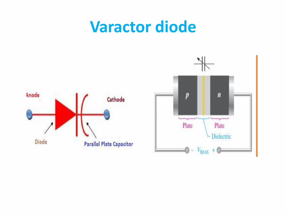
Varactor diode
Varactor diode
• Application of Varactor diode
• Parametric Amplifier & Harmonic generator
• Microwave frequency Application
• Frequency multiplier in MW Applications
• Frequency & Phase Modulator Circuit
Step recovery diode
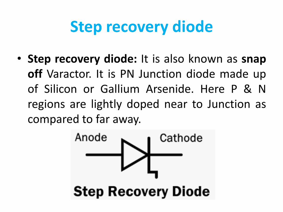
• Step recovery diode: It is also known as snap off Varactor. It is PN Junction diode made up of Silicon or Gallium Arsenide. Here P & N regions are lightly doped near to Junction as compared to far away.
Step recovery diode
• Application of Step Recovery Diode
• Frequency multiplier circuit in UHF
applications
• Power source in UHF Transmitter & Receiver
in Low range MW Frequency
• Combiner generator
• Signal generator of Lower range MW
frequencies
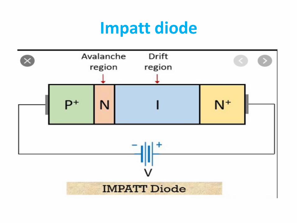
Impatt diode
• Impatt diode: It is called Impact Avalanche &
Transit Time diode. The device consists of two
copper electrodes between which P+ type, N
type & N+ type semi conducting materials are
arranged & gold wire & gold alloy contacts are
kept in between for full proof contact. It works
on the principle of Impact Avalanche & Transit
time diode. It also exhibits negative resistance
characteristics.
Impatt diode
Impatt diode
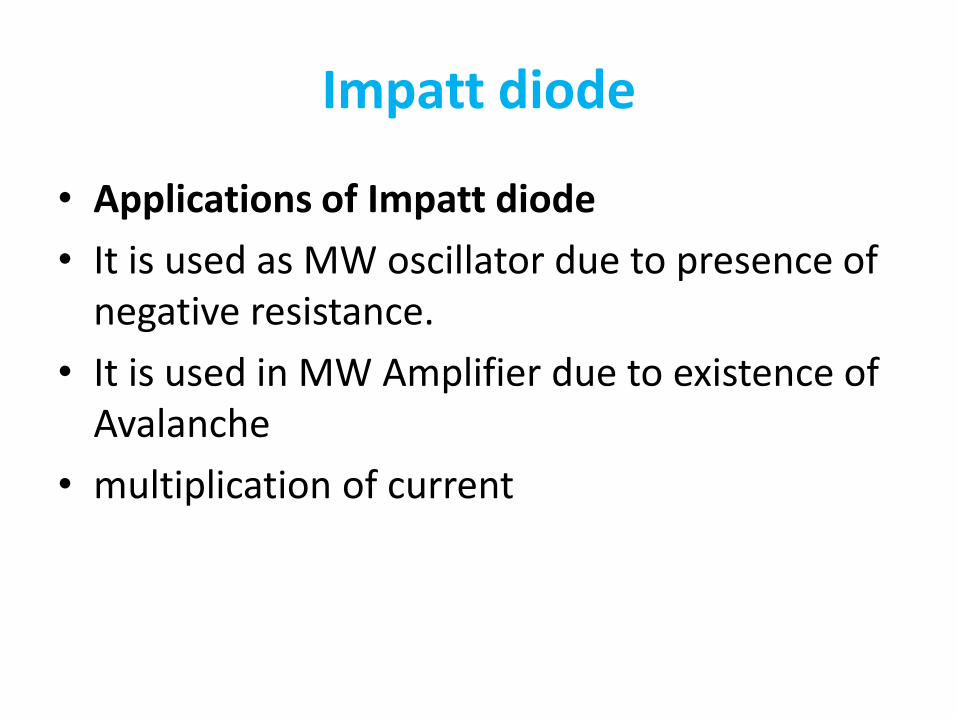
• Applications of Impatt diode
• It is used as MW oscillator due to presence of negative resistance.
• It is used in MW Amplifier due to existence of Avalanche
• multiplication of current
Tunnel diode
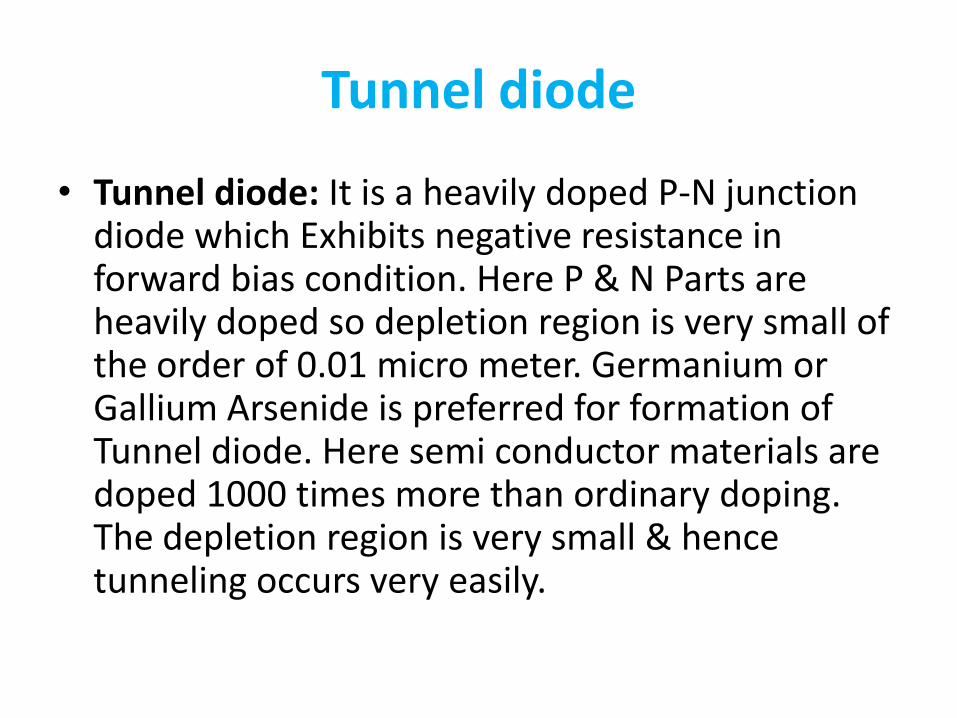
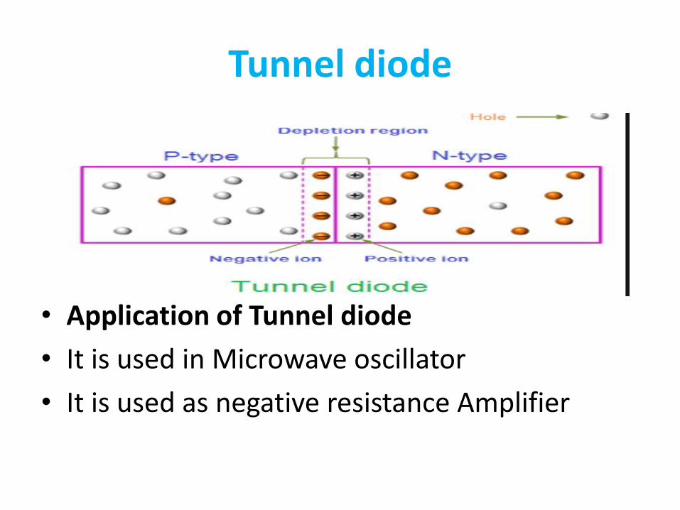
• Tunnel diode: It is a heavily doped P-N junction diode which Exhibits negative resistance in forward bias condition. Here P & N Parts are heavily doped so depletion region is very small of the order of 0.01 micro meter. Germanium or Gallium Arsenide is preferred for formation of Tunnel diode. Here semi conductor materials are doped 1000 times more than ordinary doping. The depletion region is very small & hence tunneling occurs very easily.
Tunnel diode
• Application of Tunnel diode
• It is used in Microwave oscillator
• It is used as negative resistance Amplifier
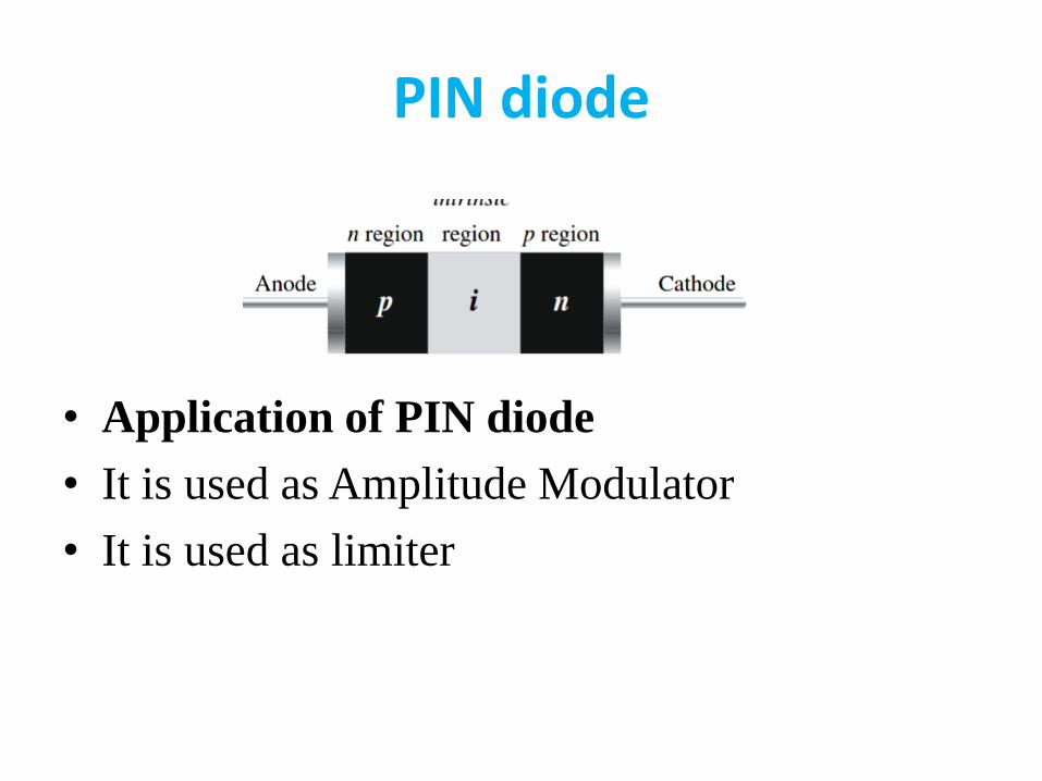
PIN diode
• PIN diode: It is a diode which contains P type Semiconductor & N type semiconductor separated by intrinsic semiconductor. It acts as ordinary diode up to a frequency of 100 MHz. It ceases to work as ordinary diode rectifier above this frequency as carrier is stored up in Intrinsic Semiconductor. At Microwave range diode acts as variable Resistance. When forward biased, Resistance varies between 1 to 10 ohm. When reverse biased, Resistance varies between 5K ohm – 10 K ohm.
PIN diode
• Application of PIN diode
• It is used as Amplitude Modulator
• It is used as limiter
GUNN diode
• GUNN diode: It is named after a scientist GUNN. Its operation does not depend on junction properties but bulk propertied of a semiconductor material. When a DC voltage in excess of 3300V/cm is applied across a thin slice of Gallium Arsenide, a negative resistance is developed in the crystal. If the slice is connected to a suitably tuned circuit, Oscillation occurs. Here oscillations occur due to Transferred electron effect or GUNN effect. GUNN effect occurs only in N type material & hence majority carriers are electrons.
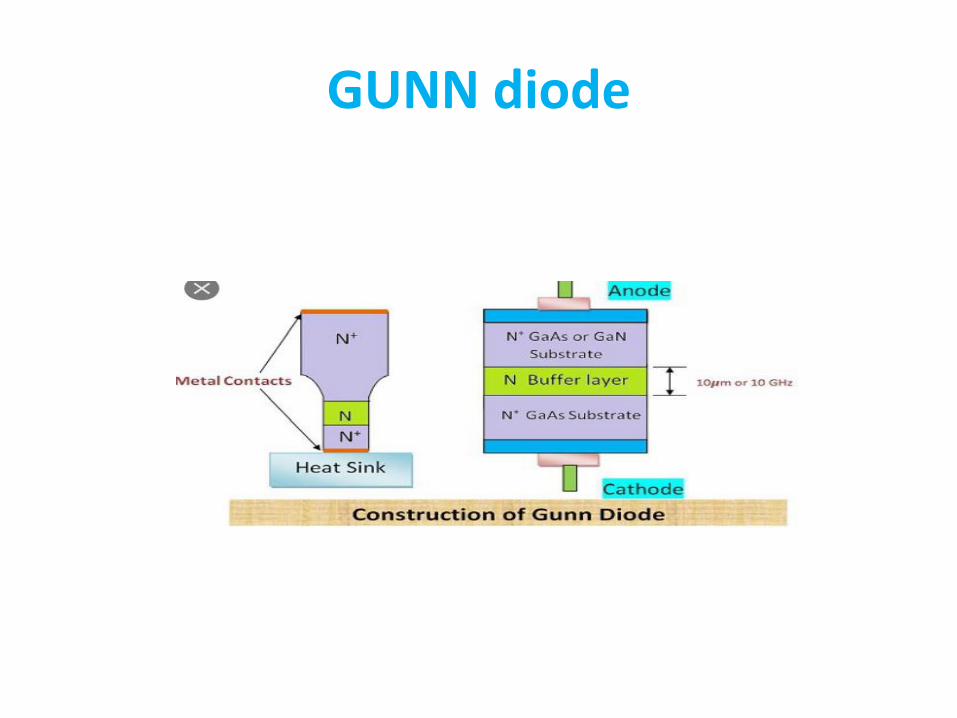
GUNN diode
GUNN diode
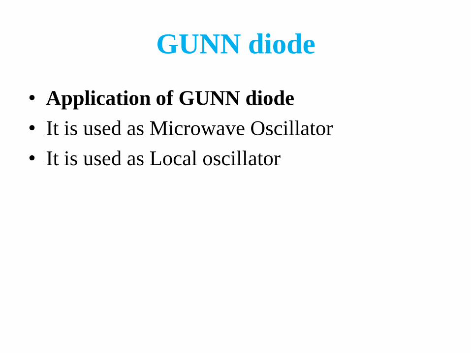
• Application of GUNN diode
• It is used as Microwave Oscillator
• It is used as Local oscillator
Zenor Diode
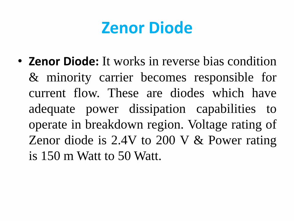
• Zenor Diode: It works in reverse bias condition
& minority carrier becomes responsible for
current flow. These are diodes which have
adequate power dissipation capabilities to
operate in breakdown region. Voltage rating of
Zenor diode is 2.4V to 200 V & Power rating
is 150 m Watt to 50 Watt.
Zenor Diode
Zenor Diode
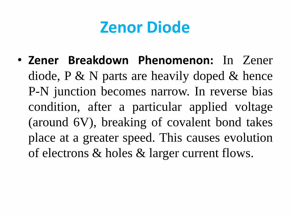
• Zener Breakdown Phenomenon: In Zener
diode, P & N parts are heavily doped & hence
P-N junction becomes narrow. In reverse bias
condition, after a particular applied voltage
(around 6V), breaking of covalent bond takes
place at a greater speed. This causes evolution
of electrons & holes & larger current flows.
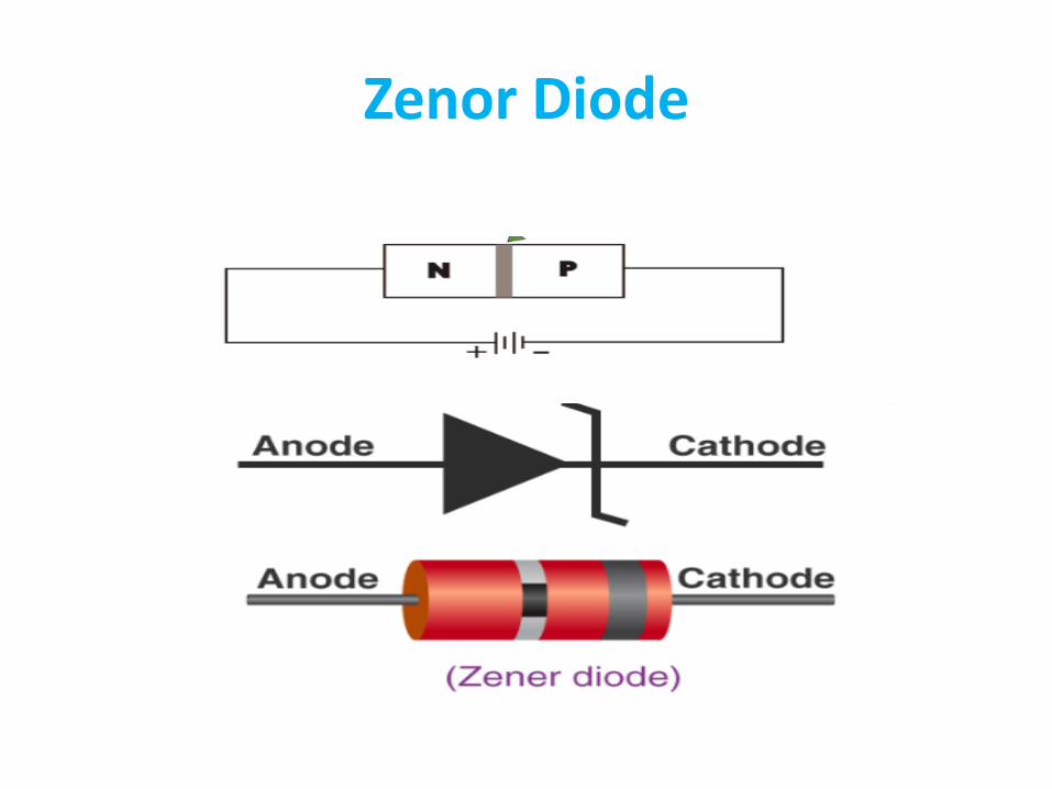
Zenor Diode
Avalanche Breakdown
• The reverse bias increases the electrical field
across the depletion region. When the high
electric field exists across the depletion, the
velocity of minority charge carrier crossing the
depletion region increases. These carriers
collide with the atoms of the crystal. Because
of the violent collision, the charge carrier takes
out the electrons from the atom.
Avalanche Breakdown
• The collision increases the electron-hole pair. As the electron-hole induces in the high electric field, they are quickly separated and collide with the other atoms of the crystals. The process is continuous, and the electric field becomes so much higher, then the reverse current starts flowing in the PN junction. The process is known as the Avalanche breakdown. After the breakdown, the junction cannot regain its original position because the diode is completely burnt off
Application of Zenor Diode
• As Voltage Regulator
• As Peak Clipper
• For meter protection against excessive voltage
• As fixed reference voltage for biasing & Comparison purpose.
Transistors
• Transistors are three terminal active devices made from different semiconductor materials that can act as either an insulator or a conductor by the application of a small signal voltage. The transistor's ability to change between these two states enables it to have two basic functions: "switching" (digital electronics) or "amplification" (analogue electronics). Then bipolar transistors have the ability to operate within three different regions:
Transistors
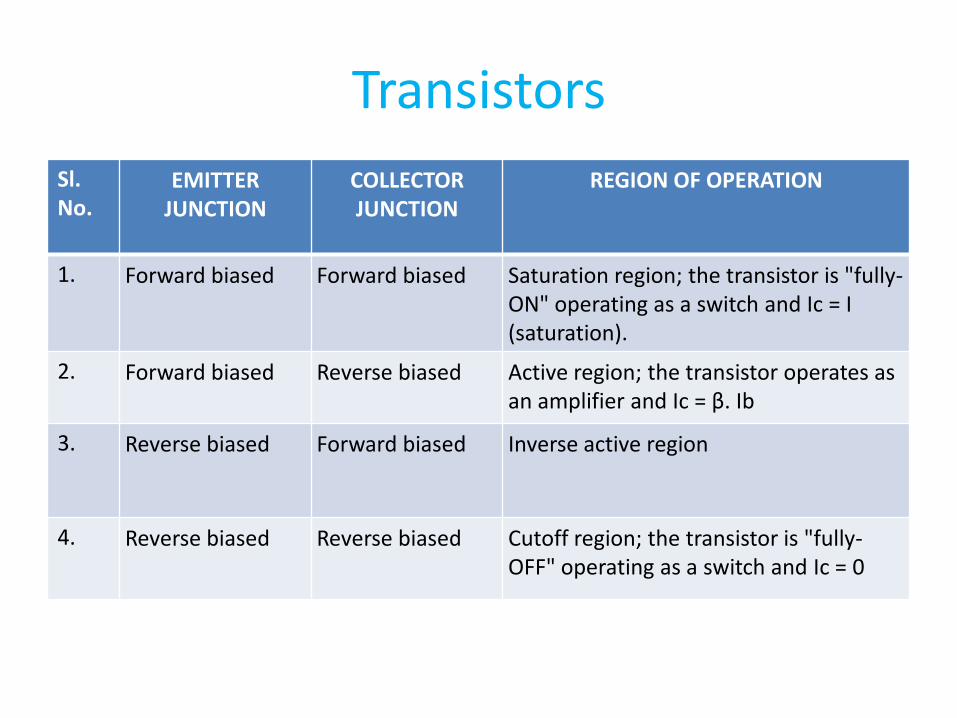
Sl. No.
EMITTER JUNCTION
COLLECTOR JUNCTION
REGION OF OPERATION
1. Forward biased Forward biased Saturation region; the transistor is "fully-ON" operating as a switch and Ic = I (saturation).
2. Forward biased Reverse biased Active region; the transistor operates as an amplifier and Ic = β. Ib
3. Reverse biased Forward biased Inverse active region
4. Reverse biased Reverse biased Cutoff region; the transistor is "fully-OFF" operating as a switch and Ic = 0
BJT
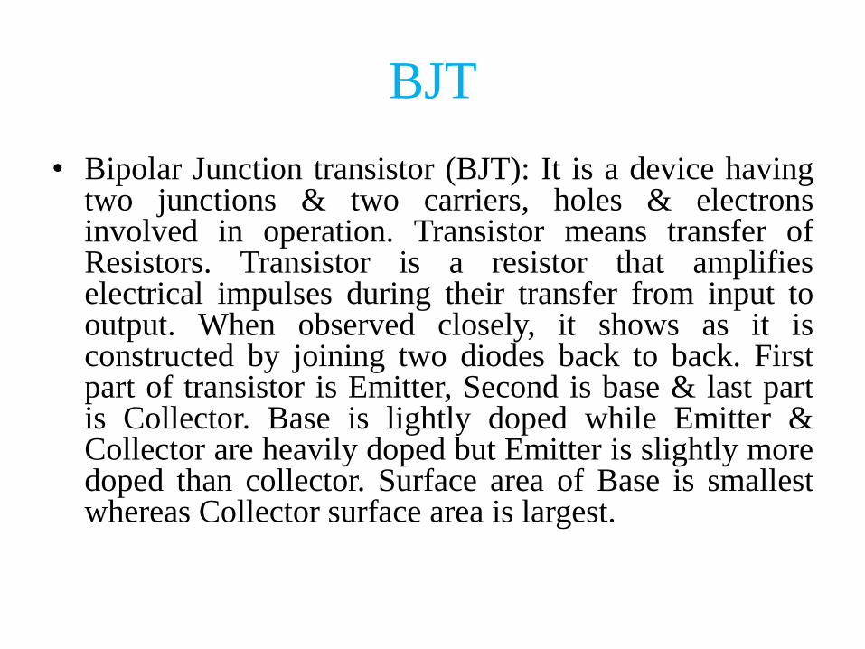
• Bipolar Junction transistor (BJT): It is a device having two junctions & two carriers, holes & electrons involved in operation. Transistor means transfer of Resistors. Transistor is a resistor that amplifies electrical impulses during their transfer from input to output. When observed closely, it shows as it is constructed by joining two diodes back to back. First part of transistor is Emitter, Second is base & last part is Collector. Base is lightly doped while Emitter & Collector are heavily doped but Emitter is slightly more doped than collector. Surface area of Base is smallest whereas Collector surface area is largest.
Transistors
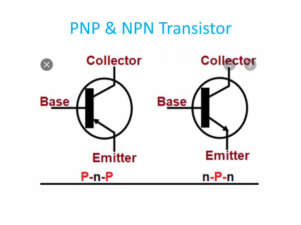
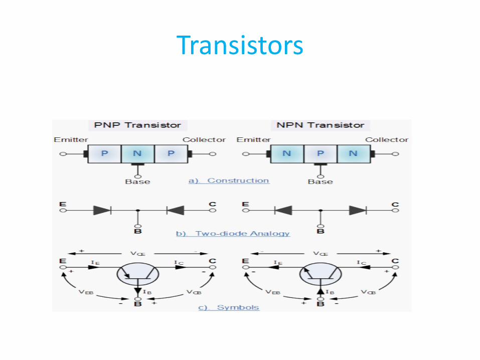
PNP & NPN Transistor
Biasing of Transistor
• For proper working Biasing is done. Biasing is nothing but applying proper DC voltage across Emitter & Collector junctions for its proper working. Current in a transistor flows when EB junction is forward biased & CB junction is reverse biased. EB junction is responsible for pushing majority carriers towards Collector & CB junction is responsible for pulling those carriers towards Collector. So biasing voltage may be adjusted in such a way that these push & pull conditions are maintained for smooth flow of current.
Biasing of Transistor
• The forward biasing of EB junction allows low resistance for emitter ckt. and reverse biasing of CB junction provides high resistance in the collector ckt., which means a weak signal is introduced in low resistance ckt. and the o/p is taken from the high resistance ckt.. So a transistor transfer a signal from low resistance to high resistance.
•
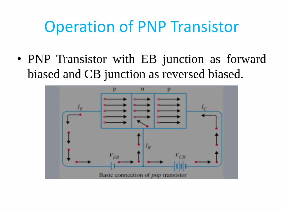
Operation of PNP Transistor
• PNP Transistor with EB junction as forward
biased and CB junction as reversed biased.
Operation of PNP Transistor
• The holes of P-region is repelled by the positive terminal of battery VEB towards base.
• As holes reaches the collector electrode, an electron is emitted from the negative terminal of battery and neutralize the hole which results in breaking down of covalent bond near the emitter electrode. The librated electron enters the positive terminal of battery VEB while the hole immediately moves towards the emitter junction.
• Conduction within PNP transistor takes place due to holes and in external ckt. due to electrons.
Operation of PNP Transistor
• The width of base region is very thin and it is
lightly doped and hence only 2% to 5% of
holes recombine with the free electron of N
region. This constitute the base current IB
which is very small.
• Thus IE = IC + IB
Transistor as an Amplifier
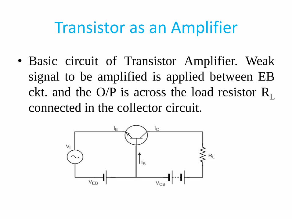
• Basic circuit of Transistor Amplifier. Weak
signal to be amplified is applied between EB
ckt. and the O/P is across the load resistor RL
connected in the collector circuit.
Principle of Operation
• Principle of Operation : In Active mode of transistor working, EB Junction is forward bias & BC Junction is reverse bias. At forward Junction, Emitter injects majority carrier to Base region. Some majority carrier is lost due to recombination of electrons & holes in Base region. The excess carriers diffuse across Base to Collector Junction. As collector junction is reverse Biased, diffused carriers are collected at Collector.
Transistor Configuration
• As the Bipolar Transistor is a three terminal
device, there are basically three possible ways
to connect it within an electronic circuit with
one terminal being common to both the input
and output.
• Common Base Configuration
• Common Emitter Configuration
• Common Collector configuration
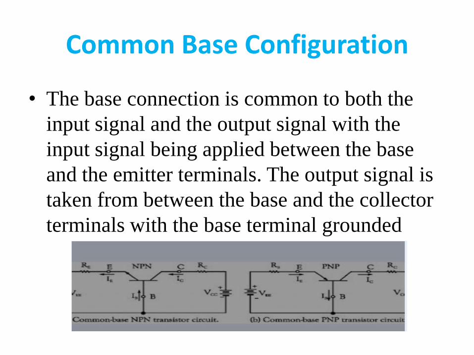
Common Base Configuration
• The base connection is common to both the
input signal and the output signal with the
input signal being applied between the base
and the emitter terminals. The output signal is
taken from between the base and the collector
terminals with the base terminal grounded
Common Base Configuration
• In Active region, when Emitter current is Zero, Collector current is small equal to Reverse Saturation current. When Emitter current increases, Collector Current also increases i.e. Collector current is independent of Collector voltage & depends on Emitter current. In saturation region, Forward Biasing of Collector accounts for large change in Collector current for a small change in Collector Voltage.
• Current amplification factor α = - IC/ IE
• CB has Voltage Gain but no Current Gain
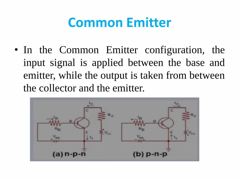
Common Emitter
• In the Common Emitter configuration, the
input signal is applied between the base and
emitter, while the output is taken from between
the collector and the emitter.
Common Emitter Configuration
• In saturation region, Collector Current is independent of Base Current & depends on Load Resistance.
• Base Current amplification factor β = IC/ IB
• CE has both Current and Voltage Gain
Common Collector
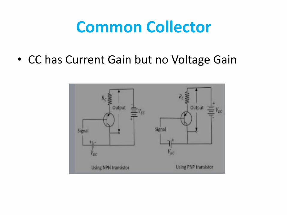
• CC has Current Gain but no Voltage Gain
Common Collector Configuration
• In the CC or grounded collector configuration, the collector is common through the supply. The input signal is connected directly to the base, while the output is taken from the emitter load. This type of configuration is commonly known as a Voltage Follower or Emitter Follower circuit. The emitter follower configuration is very useful for impedance matching applications because of the very high input impedance, in the region of hundreds of thousands of Ohms while having a relatively low output impedance
• Current amplification factor α = IE/ IB
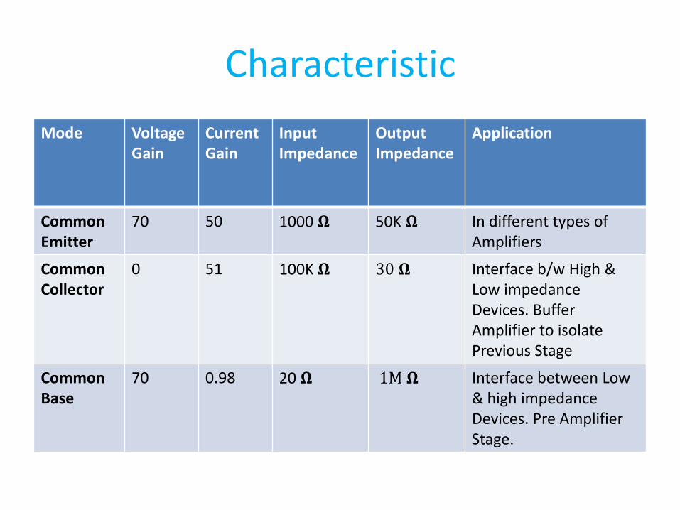
Characteristic
Mode Voltage Gain
Current Gain
Input Impedance
Output Impedance
Application
Common Emitter
70 50 1000 𝛀 50K 𝛀
In different types of Amplifiers
Common Collector
0 51 100K 𝛀
30 𝛀
Interface b/w High & Low impedance Devices. Buffer Amplifier to isolate Previous Stage
Common Base
70 0.98 20 𝛀
1M 𝛀
Interface between Low & high impedance Devices. Pre Amplifier Stage.
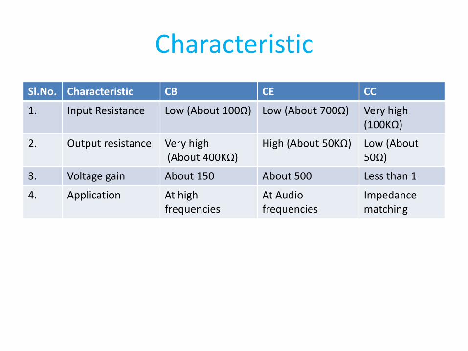
Characteristic
Sl.No. Characteristic CB CE CC
1. Input Resistance Low (About 100Ω) Low (About 700Ω)
Very high (100KΩ)
2. Output resistance Very high (About 400KΩ)
High (About 50KΩ) Low (About 50Ω)
3. Voltage gain About 150 About 500 Less than 1
4. Application At high frequencies
At Audio frequencies
Impedance matching
FET: Field Effect Transistor
• FET is a semiconductor device which
operation depends on control of current by an
electric field. In BJT operation depends on
both types of carriers i.e electrons & holes. In
FET operation depends only on either hole or
electron. This is why FET is known as Uni
polar device. BJT has low input impedance
whereas FET has high input impedance
FET: Field Effect Transistor
• Advantage of FET over BJT is • It produces lesser noise that BJT • Effect of radiation is less compared to BJT • FET has better thermal stability • FET is simpler to develop in fabrication of IC • FET is excellent signal chopper • Disadvantage of FET is that it has smaller Gain
Bandwidth product • compared to BJT. • Classification
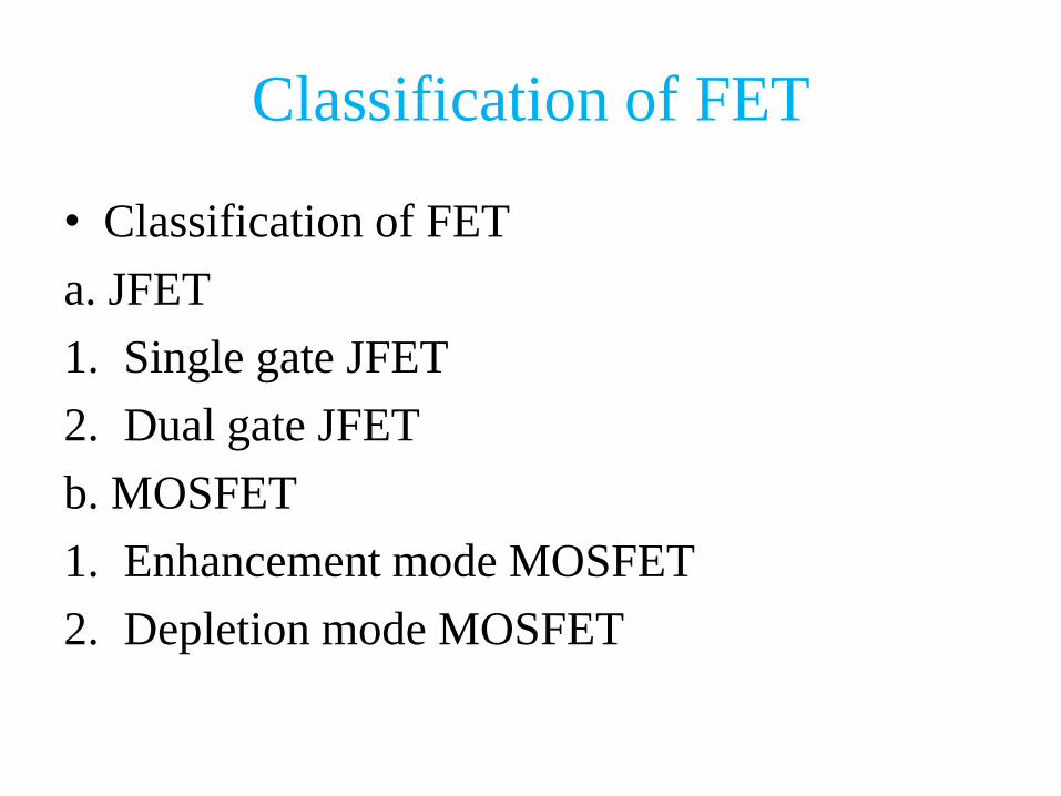
Classification of FET
• Classification of FET
a. JFET
1. Single gate JFET
2. Dual gate JFET
b. MOSFET
1. Enhancement mode MOSFET
2. Depletion mode MOSFET
Classification of FET
• Constituents of FET are
• Source: This is the terminal through which majority carriers enter the bar.
• Drain: This is the terminal through which majority carriers go out of the bar.
• Gate: This is present on both sides of channel & forms controlled electrodes.
• Channel: This is the bar sandwiched between the two gates through which majority carriers flow from Source to Drain.
SCR, DIAC, TRIAC
• A special type of semiconductor devices is called Thyristors. Thyristors means Thermal Resistors. Thyristor is a combination of two Transistors PNP & NPN. Thyristors are used in devices like Thyratron, Mercury Arc Rectifier, Excitrons, and Ignitors. Thyristor family has following devices
• SCR Silicon Controlled Rectifier
• SCS Silicon Controlled Switch
• DIAC Two Terminal bi directional PNP Switch
• TRIAC Three terminal bi directional PNPN Switch
IC: Integrated Circuit
• In IC Semi conductor circuit with elements like Active elements & Passive elements have been made along with their interconnection in a single chip & Complexities have been minimized.
• Process of IC fabrication
• Epitaxial Growth
• Isolation Diffusion
• Base Diffusion
• Emitter Diffusion
• Aluminum Metallization
• Securing & Mounting
Techniques of IC Fabrication
• Grown Junction: Here first of all a Semiconductor material like Silicon is taken. Then it is doped with a P type material. Then P type material is doped with n type material. This forms a junction diode. In case of Transistor, alternate layers of P N & P are formed by this technique.
• Diffused Junction: Here junction is produced by gaseous diffusion of P & N type material on semiconductor wafer. The junction produced by spreading method is called diffused junction.
Techniques of IC Fabrication
• Epitaxial grown Junction: In this process, on
a highly resistiveP type substrate, N type layer
is grown epitaxially in such a way that N type
material forms a continuation with P type
material. This operation is done inside a
special furnace called reactor where
temperature is around 900 to 1000 degree
centigrade.
Regulated Power Supply
• Regulated Power Supplies are those which give constant outputs in spite of fluctuation of voltage in the input.
• Functions
a. Regulation of Output Voltage
b. Keeping the Voltage constant at desired value
• Parts
a. Measuring Unit
b. Regulation Unit


![ERF L4 Passive Devices [Modo de Compatibilidad]](https://img.pdfslide.us/doc/110x75/55cf96f9550346d0338f03d4/erf-l4-passive-devices-modo-de-compatibilidad.jpg)