Embed Size (px)
DESCRIPTION
manual
Citation preview

Oscillator circuit using gates

Oscillators circuits using NAND gates Individual Sequential Logic circuits can be used to build more complex circuits such as Multivibrators, Counters, Shift Registers, Latches and Memories etc, but for these types of circuits to operate in a “sequential” way, they require the addition of a clock pulse or timing signal to cause them to change their state. Clock pulses are generally continuous square or rectangular shaped waveform that is produced by a single pulse generator circuit such as a Multivibrator.
A multivibrator circuit oscillates between a “HIGH” state and a “LOW” state producing a continuous output. Astable multivibrators generally have an even 50% duty cycle, that is that 50% of the cycle time the output is “HIGH” and the remaining 50% of the cycle time the output is “OFF”. In other words, the duty cycle for an astable timing pulse is 1:1.
Sequential logic circuits that use the clock signal for synchronization are dependant upon the frequency and and clock pulse width to activate there switching action. Sequential circuits may also change their state on either the rising or falling edge, or both of the actual clock signal as we have seen previously with the basic flip-flop circuits. The following list are terms associated with a timing pulse or waveform.
Active HIGH - if the state change occurs from a “LOW” to a “HIGH” at the clock’s pulse rising edge or during the clock width.
Clock Signal Waveform
Active LOW - if the state change occurs from a “HIGH” to a “LOW” at the clock’s pulses falling edge.
Duty Cycle - this is the ratio of the clock width to the clock period.
Clock Width - this is the time during which the value of the clock signal is equal to a logic “1″, or HIGH.
Clock Period - this is the time between successive transitions in the same direction, ie, between two rising or two falling edges.
Clock Frequency - the clock frequency is the reciprocal of the clock period, frequency = 1/clock period
Clock pulse generation circuits can be a combination of analogue and digital circuits that produce a continuous series of pulses (these are called astable multivibrators) or a pulse of a specific duration (these are called monostable multivibrators). Combining two or more of multivibrators provides generation of a desired pattern of pulses (including pulse width, time between pulses and frequency of pulses).
There are basically three types of clock pulse generation circuits:
Astable – A free-running multivibrator that has NO stable states but switches continuously between two states this action produces a train of square wave pulses at a fixed frequency.
Monostable – A one-shot multivibrator that has only ONE stable state and is triggered externally with it returning back to its first stable state.
Bistable – A flip-flop that has TWO stable states that produces a single pulse either positive or negative in value.
One way of producing a very simple clock signal is by the interconnection of logic gates. As NAND gates contains amplification, they can also be used to provide a clock signal or timing pulse with the aid of a single Capacitor and a single Resistor to provide the feedback and timing function.
These timing circuits are often used because of there simplicity and are also useful if a logic circuit is designed that has unused gates which can be utilised to create the monostable or astable oscillator. This simple type of RC Oscillator network is sometimes called a “Relaxation Oscillator”.
Monostable Multivibrator CircuitsMonostable Multivibrators or “one-shot” pulse generators are generally used to convert short sharp pulses into wider ones for timing applications. Monostable multivibrators generate a single output pulse, either “HIGH” or “LOW”, when a suitable external trigger signal or pulse T is applied. This trigger pulse signal initiates a timing cycle which causes the output of the monostable to change state at the start of the timing cycle, ( t1 ) and remain in this second state until the end of the timing period, ( t1 ) which is determined by the time constant of the timing capacitor, CT and the resistor, RT.

The monostable multivibrator now stays in this second timing state until the end of the RC time constant and automatically resets or returns itself back to its original (stable) state. Then, a monostable circuit has only one stable state. A more common name for this type of circuit is simply a “Flip-Flop” as it can be made from two cross-coupled NAND gates (or NOR gates) as we have seen previously. Consider the circuit below.
Simple NAND Gate Monostable Circuit
Suppose that initially the trigger input T is held HIGH at logic level “1″ by the resistor R1 so that the output from the first NAND gate U1 is LOW at logic level “0″, (NAND gate principals). The timing resistor, RT is connected to a voltage level equal to logic level “0″, which will cause the capacitor, CT to be discharged. The output of U1 is LOW, timing capacitor CT is completely discharged therefore junction V1 is also equal to “0″ resulting in the output from the second NAND gate U2, which is connected as an inverting NOT gate will therefore be HIGH.
The output from the second NAND gate, ( U2 ) is fed back to one input of U1 to provide the necessary positive feedback. Since the junction V1 and the output of U1 are both at logic “0″ no current flows in the capacitor CT. This results in the circuit being Stable and it will remain in this state until the trigger input T changes.
If a negative pulse is now applied either externally or by the action of the push-button to the trigger input of the NAND gate U1, the output of U1 will go HIGH to logic “1″ (NAND gate principles). Since the voltage across the capacitor cannot change instantaneously (capacitor charging principals) this will cause the junction at V1 and also the input to U2 to also go HIGH, which in turn will make the output of the NAND gate U2 change LOW to logic “0″ The circuit will now remain in this second state even if the trigger input pulse T is removed. This is known as the Meta-stable state.
The voltage across the capacitor will now increase as the capacitor CT starts to charge up from the output of U1 at a time constant determined by the resistor/capacitor combination. This charging process continues until the charging current is unable to hold the input of U2 and therefore junction V1 HIGH. When this happens, the output of U2 switches HIGH again, logic

“1″, which in turn causes the output of U1 to go LOW and the capacitor discharges into the output of U1 under the influence of resistor RT. The circuit has now switched back to its original stable state.
Thus for each negative going trigger pulse, the monostable multivibrator circuit produces a LOW going output pulse. The length of the output time period is determined by the capacitor/resistor combination (RC Network) and is given as the Time Constant T = 0.69RC of the circuit in seconds. Since the input impedance of the NAND gates is very high, large timing periods can be achieved.
As well as the NAND gate monostable type circuit above, it is also possible to build simple monostable timing circuits that start their timing sequence from the rising-edge of the trigger pulse using NOT gates, NAND gates and NOR gates connected as inverters as shown below.
NOT Gate Monostable Multivibrator
As with the NAND gate circuit above, initially the trigger input T is HIGH at a logic level “1″ so that the output from the first NOT gate U1 is LOW at logic level “0″. The timing resistor, RT and the capacitor, CT are connected together in parallel and also to the input of the second NOT gate U2. As the input to U2 is LOW at logic “0″ its output at Q is HIGH at logic “1″.
When a logic level “0″ pulse is applied to the trigger input T of the first NOT gate it changes state and produces a logic level “1″ output. The diode D1 passes this logic “1″ voltage level to the RC timing network. The voltage across the capacitor, CT increases rapidly to this new voltage level, which is also connected to the input of the second NOT gate. This in turn outputs a logic “0″ at Q and the circuit stays in this Meta-stable state as long as the trigger input T applied to the circuit remains LOW.
When the trigger signal returns HIGH, the output from the first NOT gate goes LOW to logic “0″ (NOT gate principals) and the fully charged capacitor, CT starts to discharge itself through the parallel resistor, RT connected across it. When the voltage across the capacitor drops below the lower threshold value of the input to the second NOT gate, its output switches back again

producing a logic level “1″ at Q. The diode D1 prevents the timing capacitor from discharging itself back through the first NOT gates output.
Then, the Time Constant for a NOT gate Monostable Multivibrator is given as T = 0.8RC + Trigger in seconds.
One main disadvantage of Monostable Multivibrators is that the time between the application of the next trigger pulse T has to be greater than the RC time constant of the circuit.
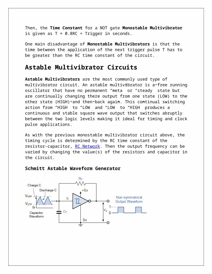
Astable Multivibrator CircuitsAstable Multivibrators are the most commonly used type of multivibrator circuit. An astable multivibrator is a free running oscillator that have no permanent “meta” or “steady” state but are continually changing there output from one state (LOW) to the other state (HIGH) and then back again. This continual switching action from “HIGH” to “LOW” and “LOW” to “HIGH” produces a continuous and stable square wave output that switches abruptly between the two logic levels making it ideal for timing and clock pulse applications.
As with the previous monostable multivibrator circuit above, the timing cycle is determined by the RC time constant of the resistor-capacitor, RC Network. Then the output frequency can be varied by changing the value(s) of the resistors and capacitor in the circuit.
Schmitt Astable Waveform Generator
Assuming that the timing capacitor, CT is fully discharged and the input to the Schmitt trigger is at logic “0″, therefore its output is at logic “1″, the capacitor will start to charge up exponentially through the timing resistor, RT from right to left. The speed at which the capacitor charges will depend upon their RC time constant.
At some point, the voltage across the capacitors plates will reach the higher threshold value of the Schmitt trigger causing the output to switch from a logic “1″ to a logic “0″. As the output from the Schmitt trigger is effectively at a 0v potential, the capacitor starts to discharge back

through the timing resistor, RT from left to right at a speed determined by their RC timing constant.
When the voltage across the plates of the discharging capacitor reaches the lower threshold value of the Schmitt trigger, it causes it to change state and the whole process repeats.
Generally, the higher threshold point, VHTP typically occurs around the 65% (2/3rds) of the supply voltage while the lower threshold point occurs around 35% (1/3rd) of the supply voltage. Any Schmitt trigger inverter such as the 4106, 4584, 74LS14, 74LS19, etc can be used to generate a timing signal or even Schmitt NAND gates such as the 4093, 74LS132, etc.
However, using different logic families whether CMOS or TTL (74LSxx, 74HLSxx, 74HCTxx) will result in different upper and lower trip points resulting in differing operating frequencies and mark-to-space ratios of the output timing waveform. Generally the error in the oscillating frequency for different logic sub-families is not a problem especially at higher frequencies, but can be anywhere from 1.2RC to 1.5RC with the generalised formula for a Schmitt astable waveform generator given as:
Schmitt Waveform Frequency
Where: Beta ( β ) can be any fixed value between 1.2 and 1.5 depending upon the logic gate family used.
If we replace the fixed timing resistor, RT with a potentiometer, a variable frequency square wave timing signal can be produced for our Christmas lights sequencer circuit. Obviously we do not want the value of the timing resistance to be equal to zero when the potentiometer is turned fully in one direction as this would short out the Schmitt inverter. So to prevent this from happening a small value fixed resistance needs to be connected in series with the potentiometer to provide at least some timing resistance.
The components of the timing RC network used in a Christmas lights sequencer can be any values you have available to produce the oscillating frequency of your choice. The following Schmitt astable circuit would give an output frequency ranging from about 10Hz to 6kHz when the potentiometer is adjusted from minimum to maximum. An additional Schmitt trigger inverter IC1b is used as an inverting buffer to help clean up the timing waveform and improve the performance of the oscillator. As there are six inverters per 40106B IC, there are sufficient spare.
Christmas Lights Sequencer Waveform Generator
Ok, now we have a decade counter and an astable waveform oscillator circuit we now need some lights to make up our novelty Christmas lights sequencer circuit. These can be any type of lamps or lights you have available from LED’s to miniature filament lamps. If you so wished the output from the counter could also be used to drive Optocoupler which in turn could be used to switch Triacs or Thyristors for switching mains voltage lamps. For this simple Christmas lights sequencer tutorial we will use LED’s.
The 4017B decade counter has ten fully decoded outputs with each one capable of switching up to 20mA. Each of the decoded outputs is normally LOW (logic “0″) and switches HIGH (logic “1″) one at a time sequentially. The advantage here is that we can use each output to drive a single LED directly and better still as only one LED is illuminated at any one time, only one current limiting resistor is required for all 10 LED’s as shown.