Embed Size (px)
Citation preview
An RF amplifier stage is not onlyclassified by amplification, which is ashigh as possible, and thus by its maxi-mum output. What is frequently nottaken into account, but is decisive forthe signal quality, is the inter-modula-tion performance.In practice, because of the gain char-acteristic, which is not completely lin-ear, RF amplifiers are bound to pro-duce distortion. A standard methodfor measuring this inter-modulation,e.g. in SSB amplifiers, is the 2-tonemeasurement. TV engineering uses a3-tone measuring procedure!
1.General
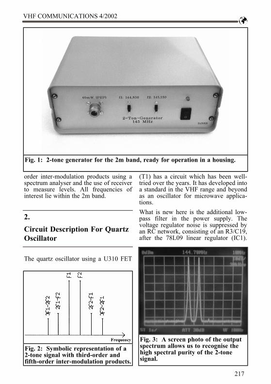
In order to measure the inter-modulationbehaviour of an amplifier stage, twosignals of equal strength with frequenciesf1 and f2 are applied to the input of thisstage. The amplifier produces a spectrumof inter-modulation products from thesesignals. Particularly critical in practiceare the third order (2f1-f2; 2f2-f1) and ofthe fifth order (3f1-2f2; 3f2-2f1).Fig. 2 gives a graphical representation ofthe position of these inter-modulationproducts.
The objective, e.g. in SSB amplifiers, isto ensure that the third-order inter-modu-lation products are below 40dB in rela-tion to the pure tone. Considerablytighter values apply to pre-stages andmixers. Should these quality criteria notbe taken into account in design of anSSB transmitter, it leads to poor modula-tion quality and a broad signal. Forreceiver pre-stages, this lack of quality isclearly shown by the so-called “plugeffect”.To be able to measure the inter-modula-tion products, the 2-tone generator mustitself produce a high-quality signal.The equipment described here com-pletely fulfils this requirement (Fig. 3).The output level is +10dBm (10mW) foreach pure tone.The selection of this signal level repre-sents a compromise between acceptablecost and versatility. Thus the 2-tonegenerator can be used in the same wayfor measurements on pre-amplifiers andtransmitting amplifiers. Should a higheroutput level be required, then a suitablepower amplifier can be used with the2-tone generator for 145MHz. OMCarsten Vieland (DJ4GC) has alreadytackled this subject some years ago in[5].The two frequencies, f1 = 144.850MHzand f2 = 145.150MHz, permit both themeasurement of the third-order and fifth-
Wolfgang Schneider, DJ8ES
2-Tone Generator For 145Mhz
VHF COMMUNICATIONS 4/2002
216
order inter-modulation products using aspectrum analyser and the use of receiverto measure levels. All frequencies ofinterest lie within the 2m band.
2.Circuit Description For QuartzOscillator
The quartz oscillator using a U310 FET
(T1) has a circuit which has been well-tried over the years. It has developed intoa standard in the VHF range and beyondas an oscillator for microwave applica-tions.What is new here is the additional low-pass filter in the power supply. Thevoltage regulator noise is suppressed byan RC network, consisting of an R3/C19,after the 78L09 linear regulator (IC1).
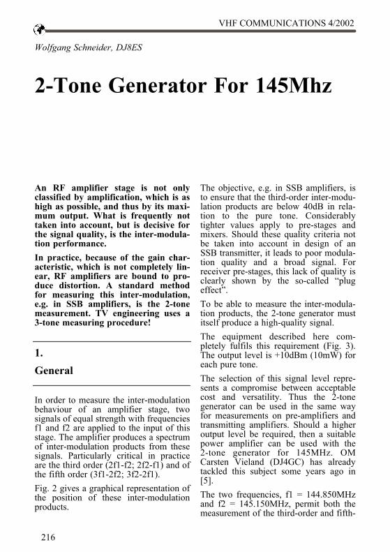
Fig. 1: 2-tone generator for the 2m band, ready for operation in a housing.
Fig. 2: Symbolic representation of a2-tone signal with third-order andfifth-order inter-modulation products.
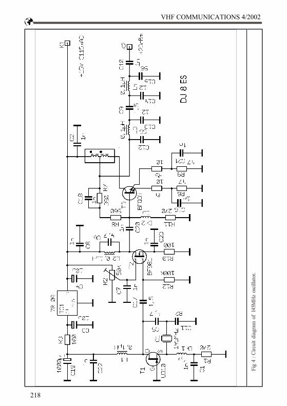
Fig. 3: A screen photo of the outputspectrum allows us to recognise thehigh spectral purity of the 2-tonesignal.
VHF COMMUNICATIONS 4/2002
217
VHF COMMUNICATIONS 4/2002
218
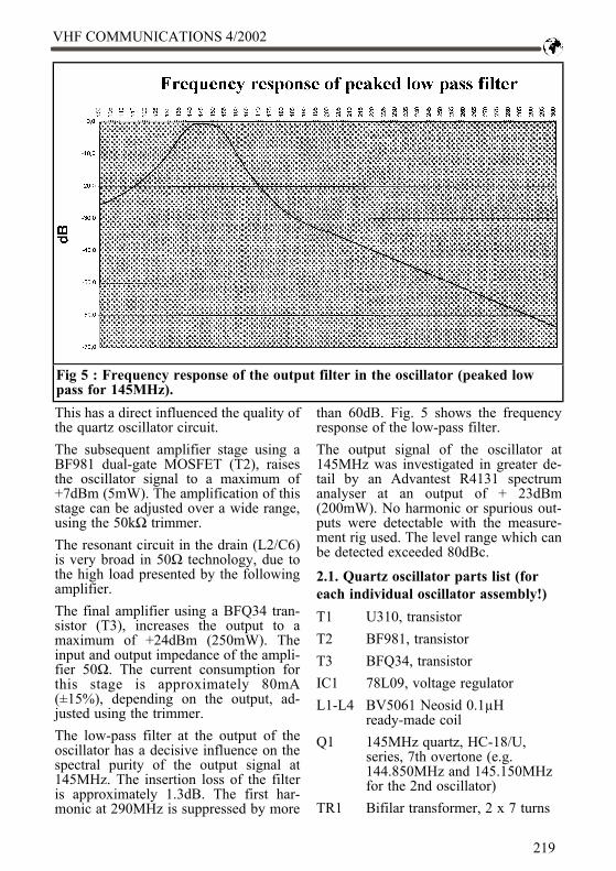
This has a direct influenced the quality ofthe quartz oscillator circuit.The subsequent amplifier stage using aBF981 dual-gate MOSFET (T2), raisesthe oscillator signal to a maximum of+7dBm (5mW). The amplification of thisstage can be adjusted over a wide range,using the 50kΩ trimmer.The resonant circuit in the drain (L2/C6)is very broad in 50Ω technology, due tothe high load presented by the followingamplifier.The final amplifier using a BFQ34 tran-sistor (T3), increases the output to amaximum of +24dBm (250mW). Theinput and output impedance of the ampli-fier 50Ω. The current consumption forthis stage is approximately 80mA(±15%), depending on the output, ad-justed using the trimmer.The low-pass filter at the output of theoscillator has a decisive influence on thespectral purity of the output signal at145MHz. The insertion loss of the filteris approximately 1.3dB. The first har-monic at 290MHz is suppressed by more
than 60dB. Fig. 5 shows the frequencyresponse of the low-pass filter.The output signal of the oscillator at145MHz was investigated in greater de-tail by an Advantest R4131 spectrumanalyser at an output of + 23dBm(200mW). No harmonic or spurious out-puts were detectable with the measure-ment rig used. The level range which canbe detected exceeded 80dBc.
2.1. Quartz oscillator parts list (foreach individual oscillator assembly!)T1 U310, transistorT2 BF981, transistorT3 BFQ34, transistorIC1 78L09, voltage regulatorL1-L4 BV5061 Neosid 0.1µH
ready-made coilQ1 145MHz quartz, HC-18/U,
series, 7th overtone (e.g.144.850MHz and 145.150MHzfor the 2nd oscillator)
TR1 Bifilar transformer, 2 x 7 turns
Fig 5 : Frequency response of the output filter in the oscillator (peaked lowpass for 145MHz).
VHF COMMUNICATIONS 4/2002
219
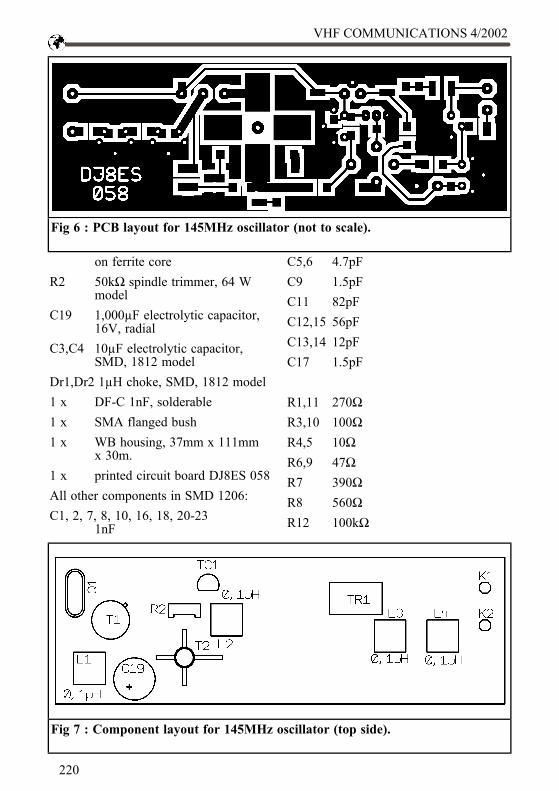
on ferrite coreR2 50kΩ spindle trimmer, 64 W
modelC19 1,000µF electrolytic capacitor,
16V, radialC3,C4 10µF electrolytic capacitor,
SMD, 1812 modelDr1,Dr2 1µH choke, SMD, 1812 model1 x DF-C 1nF, solderable1 x SMA flanged bush1 x WB housing, 37mm x 111mm
x 30m.1 x printed circuit board DJ8ES 058All other components in SMD 1206:C1, 2, 7, 8, 10, 16, 18, 20-23
1nF
C5,6 4.7pFC9 1.5pFC11 82pFC12,15 56pFC13,14 12pFC17 1.5pF
R1,11 270ΩR3,10 100ΩR4,5 10ΩR6,9 47ΩR7 390ΩR8 560ΩR12 100kΩ
Fig 6 : PCB layout for 145MHz oscillator (not to scale).
Fig 7 : Component layout for 145MHz oscillator (top side).
VHF COMMUNICATIONS 4/2002
220
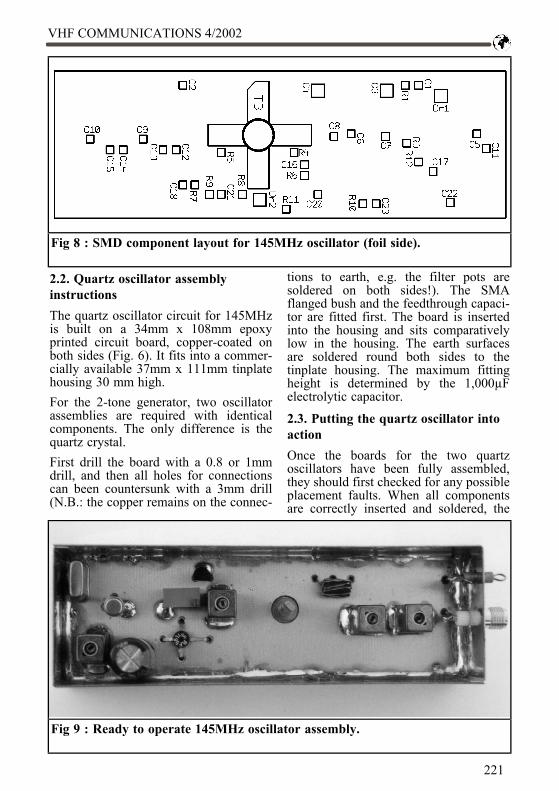
2.2. Quartz oscillator assemblyinstructionsThe quartz oscillator circuit for 145MHzis built on a 34mm x 108mm epoxyprinted circuit board, copper-coated onboth sides (Fig. 6). It fits into a commer-cially available 37mm x 111mm tinplatehousing 30 mm high.For the 2-tone generator, two oscillatorassemblies are required with identicalcomponents. The only difference is thequartz crystal.First drill the board with a 0.8 or 1mmdrill, and then all holes for connectionscan been countersunk with a 3mm drill(N.B.: the copper remains on the connec-
tions to earth, e.g. the filter pots aresoldered on both sides!). The SMAflanged bush and the feedthrough capaci-tor are fitted first. The board is insertedinto the housing and sits comparativelylow in the housing. The earth surfacesare soldered round both sides to thetinplate housing. The maximum fittingheight is determined by the 1,000µFelectrolytic capacitor.
2.3. Putting the quartz oscillator intoactionOnce the boards for the two quartzoscillators have been fully assembled,they should first checked for any possibleplacement faults. When all componentsare correctly inserted and soldered, the
Fig 8 : SMD component layout for 145MHz oscillator (foil side).
Fig 9 : Ready to operate 145MHz oscillator assembly.
VHF COMMUNICATIONS 4/2002
221
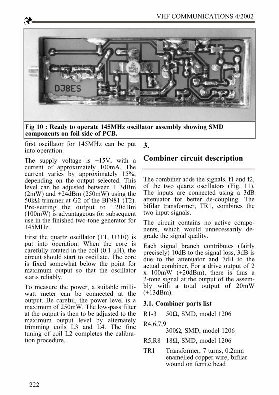
first oscillator for 145MHz can be putinto operation.The supply voltage is +15V, with acurrent of approximately 100mA. Thecurrent varies by approximately 15%,depending on the output selected. Thislevel can be adjusted between + 3dBm(2mW) and +24dBm (250mW) using the50kΩ trimmer at G2 of the BF981 (T2).Pre-setting the output to +20dBm(100mW) is advantageous for subsequentuse in the finished two-tone generator for145MHz.First the quartz oscillator (T1, U310) isput into operation. When the core iscarefully rotated in the coil (0.1 µH), thecircuit should start to oscillate. The coreis fixed somewhat below the point formaximum output so that the oscillatorstarts reliably.To measure the power, a suitable milli-watt meter can be connected at theoutput. Be careful, the power level is amaximum of 250mW. The low-pass filterat the output is then to be adjusted to themaximum output level by alternatelytrimming coils L3 and L4. The finetuning of coil L2 completes the calibra-tion procedure.
3.Combiner circuit description
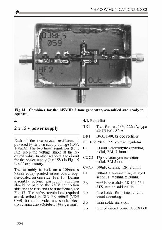
The combiner adds the signals, f1 and f2,of the two quartz oscillators (Fig. 11).The inputs are connected using a 3dBattenuator for better de-coupling. Thebifilar transformer, TR1, combines thetwo input signals.The circuit contains no active compo-nents, which would unnecessarily de-grade the signal quality.Each signal branch contributes (fairlyprecisely) 10dB to the signal loss, 3dB isdue to the attenuator and 7dB to theactual combiner. For a drive output of 2x 100mW (+20dBm), there is thus a2-tone signal at the output of the assem-bly with a total output of 20mW(+13dBm).
3.1. Combiner parts listR1-3 50Ω, SMD, model 1206R4,6,7,9
300Ω, SMD, model 1206R5,R8 18Ω, SMD, model 1206TR1 Transformer, 7 turns, 0.2mm
enamelled copper wire, bifilarwound on ferrite bead
Fig 10 : Ready to operate 145MHz oscillator assembly showing SMDcomponents on foil side of PCB.
VHF COMMUNICATIONS 4/2002
222

3 x SMA flanged bush1 x tinplate housing, 37mm x 55mm
x 30mm1 x printed circuit board DJ8ES 059
3.2. Combiner assembly instructionsThe combiner assembly is constructed ona 34mm x 54mm epoxy printed circuitboard, copper-coated on both sides (Fig.12). It fits into a commercially available37mm x 55.5mm x 30mm tinplate hous-ing.The printed circuit board is assembledfrom the foil side only, 0.8mm holes arefirst drilled for the transformer, TR1.Apart from the connection to earth, these
holes are countersunk on the earth sur-face using a 3mm drill. The connectionto earth is soldered on both sides.Before the assembly in accordance withthe assembly drawing in Fig. 13, theprinted circuit board is inserted into thetinplate housing with the SMA socketsalready fitted. The earth surfaces shouldbe soldered to the housing rim on bothsides.Anyone who cannot afford the cost ofspecial 50Ω resistors can use100Ω resis-tors in parallel (piggyback). For reasonsof symmetry, these resistors should bemeasured as precisely as possible inadvance!
Fig 11 : Circuit diagram of combiner for two frequencies in 2m band.
Fig 12 : PCB layout for combiner(not to scale).
Fig 13 : Component layout for thecombiner, all components aremounted on the foil side.
VHF COMMUNICATIONS 4/2002
223
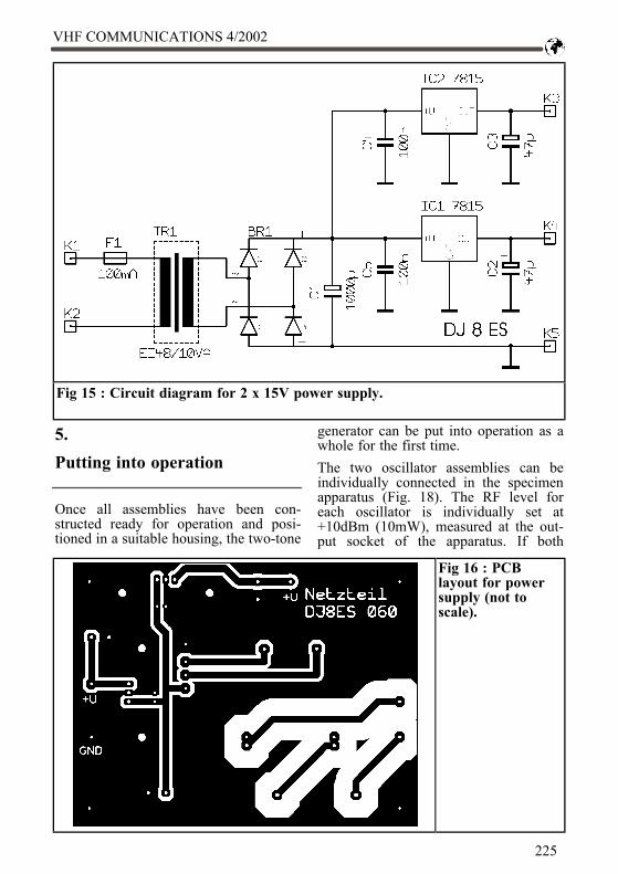
4.2 x 15 v power supply
Each of the two crystal oscillators ispowered by its own supply voltage (15V,100mA). The two linear regulators (IC1,IC2) keep the voltage stable at the re-quired value. In other respects, the circuitfor the power supply (2 x 15V) in Fig. 15is self-explanatory.The assembly is built on a 100mm x75mm epoxy printed circuit board, cop-per-coated on one side (Fig. 16). Duringassembly set-up, particular attentionshould be paid to the 230V connectionside and the fuse and the transformer, seeFig 17. The safety regulations requiredare described in DIN EN 60065 (VDE0860) for audio, video and similar elec-tronic apparatus (October, 1998 version).
4.1. Parts listTR1 Transformer, 18V, 555mA, type
EI48/16.8 10 VABR1 B40C1500, bridge rectifierIC1,IC2 7815, 15V voltage regulatorC1 1,000µF electrolytic capacitor,
radial, RM, 7.5mm.C2,C3 47µF electrolytic capacitor,
radial, RM 5mm.C4,C5 100nF, ceramic, RM 2.5mm.F1 100mA fine-wire fuse, delayed
action, D = 5mm. x 20mm.2 x profile heat sinks SK 104 38.1
STS, can be soldered in1 x fuse holder for printed circuit
board mounting5 x 1mm soldering studs1 x printed circuit board DJ8ES 060
Fig 14 : Combiner for the 145MHz 2-tone generator, assembled and ready tooperate.
VHF COMMUNICATIONS 4/2002
224
5.Putting into operation
Once all assemblies have been con-structed ready for operation and posi-tioned in a suitable housing, the two-tone
generator can be put into operation as awhole for the first time.The two oscillator assemblies can beindividually connected in the specimenapparatus (Fig. 18). The RF level foreach oscillator is individually set at+10dBm (10mW), measured at the out-put socket of the apparatus. If both
Fig 15 : Circuit diagram for 2 x 15V power supply.
Fig 16 : PCBlayout for powersupply (not toscale).
VHF COMMUNICATIONS 4/2002
225
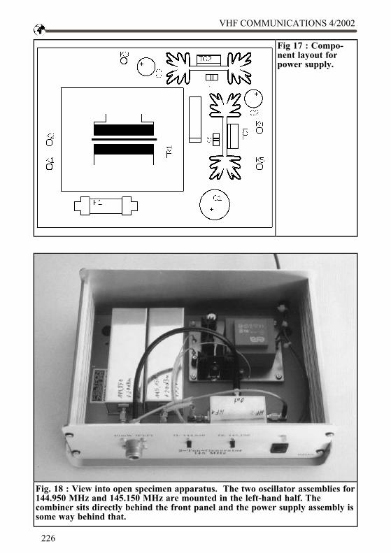
Fig 17 : Compo-nent layout forpower supply.
Fig. 18 : View into open specimen apparatus. The two oscillator assemblies for144.950 MHz and 145.150 MHz are mounted in the left-hand half. Thecombiner sits directly behind the front panel and the power supply assembly issome way behind that.
VHF COMMUNICATIONS 4/2002
226
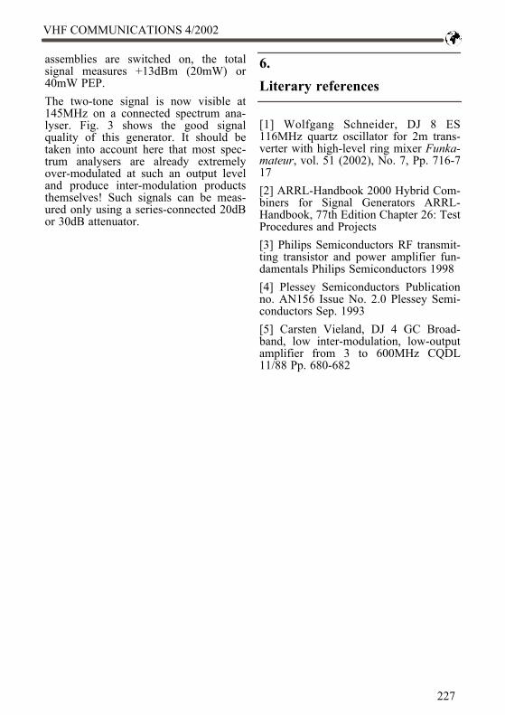
assemblies are switched on, the totalsignal measures +13dBm (20mW) or40mW PEP.The two-tone signal is now visible at145MHz on a connected spectrum ana-lyser. Fig. 3 shows the good signalquality of this generator. It should betaken into account here that most spec-trum analysers are already extremelyover-modulated at such an output leveland produce inter-modulation productsthemselves! Such signals can be meas-ured only using a series-connected 20dBor 30dB attenuator.
6.Literary references
[1] Wolfgang Schneider, DJ 8 ES116MHz quartz oscillator for 2m trans-verter with high-level ring mixer Funka-mateur, vol. 51 (2002), No. 7, Pp. 716-717[2] ARRL-Handbook 2000 Hybrid Com-biners for Signal Generators ARRL-Handbook, 77th Edition Chapter 26: TestProcedures and Projects[3] Philips Semiconductors RF transmit-ting transistor and power amplifier fun-damentals Philips Semiconductors 1998[4] Plessey Semiconductors Publicationno. AN156 Issue No. 2.0 Plessey Semi-conductors Sep. 1993[5] Carsten Vieland, DJ 4 GC Broad-band, low inter-modulation, low-outputamplifier from 3 to 600MHz CQDL11/88 Pp. 680-682
VHF COMMUNICATIONS 4/2002
227