Embed Size (px)
Citation preview
Materials Science and Engineering B74 (2000) 269–275
Optoelectronics-VLSI system integrationTechnological challenges
Marc P.Y. Desmulliez *Department of Computing and Electrical Engineering, Heriot–Watt Uni6ersity, Riccarton, Edinburgh, EH14 4AS, UK
Abstract
Hybrid VLSI-optoelectronics, also called smart-pixel technology, exploits the respective strengths of optics and electronicprocessing for the production of optical information processing systems of high performance. The recent integration ofmicron-size optoelectronic components such as emitters, photodetectors and spatial light modulators within VLSI electronic chipsallows the fabrication of on/off chip data communication rate systems of the order of 1012 pin-Hz. This aggregate rate is at leastone order of magnitude higher than is presently achievable in electronics alone. Several issues, however, remain to be resolved inorder to fully benefit from this technology. These include the relevance of optics in information processing in general andcomputer science in particular, the design and choice of the logic complexity of the electronic circuitry, its interfacing withoptoelectronic components, the assembly and testing of the resulting systems. These technological challenges are discussed in thisarticle in the light of the rapid progress achieved in this field. © 2000 Elsevier Science S.A. All rights reserved.
Keywords: Smart-pixel technology; Optical interconnects; Hybrid-VLSI optoelectronics; Optical information processing; Optical computing;Optoelectronics
www.elsevier.com/locate/mseb
1. Introduction
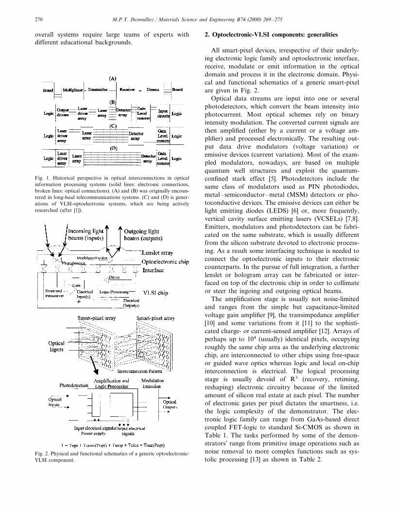
Over the last 15 years, the optoelectronic communityhas witnessed a constant drive towards the full integra-tion of optoelectronic components within their associ-ated VLSI electronic processing circuitry. This trend,originally fuelled by the long-haul telecommunicationsindustry, (A) in Fig. 1, was geared towards the fabrica-tion of OEICs (Opto-Electronic Intergrated Circuits)[1]. More recently, the need for more aggregate databandwidth in optical information processing systemshas initiated numerous industrial and academic re-search in the design and fabrication of interboard,inter- and intra-chip interconnection schemes. The re-sulting devices ((C) and (D), Fig. 1), called smart pixelsor optoelectronics-VLSI components, benefit from thestrengths of optics in data transmission (huge I/O pho-tonic density, immunity to electromagnetic interference,large fan-out capability, automatic impedance match-ing, power savings at long distance, real-time re-configurability) and the processing power of VLSI
electronic circuits [2,3]. Today, demonstrators based onthis technology exhibit the same aggregate bandwidthas that foreseen with electronic systems for the year2007 [4]. This remarkable achievement is rendered pos-sible by a variety of factors: (1) the integration ofmicron-size optoelectronic transceivers with VLSI cir-cuits; (2) the massive parallelism offered by free-spaceoptics; (3) a better understanding of the added-value ofoptics in information processing systems; and (4) theprogress in low-cost optical assembly, testing and pack-aging. In all these domains, however, technologicalissues mar the full potential of this technology: (1) theinterface of optoelectronics with silicon-based VLSIcircuits is still technologically immature; (2) the align-ment and fabrication limitations faced by free-spaceoptical components could be bettered by the adoptionof existing solutions and established standards; (3) theslow progress in adopting optics in computer architec-ture is symptomatic of the general lack of knowledge ofoptics by computer scientists as well as the ignorance ofcomputer science by optical engineers; (4) the difficultyin assembling and testing fully functional prototypes isdue to the requirement of feeding a vast amount ofvector tests; and (5) the inter-disciplinary nature of
* Tel.: +44-131-4513340; fax: +44-131-4513327.E-mail address: [email protected] (M.P.Y. Desmulliez)
0921-5107/00/$ - see front matter © 2000 Elsevier Science S.A. All rights reserved.PII: S0921 -5107 (99 )00574 -7
M.P.Y. Desmulliez / Materials Science and Engineering B74 (2000) 269–275270
overall systems require large teams of experts withdifferent educational backgrounds.
2. Optoelectronic-VLSI components: generalities
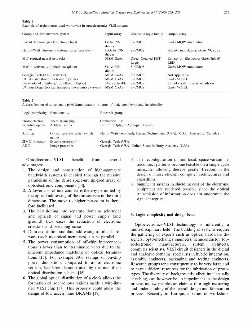
All smart-pixel devices, irrespective of their underly-ing electronic logic family and optoelectronic interface,receive, modulate or emit information in the opticaldomain and process it in the electronic domain. Physi-cal and functional schematics of a generic smart-pixelare given in Fig. 2.
Optical data streams are input into one or severalphotodetectors, which convert the beam intensity intophotocurrent. Most optical schemes rely on binaryintensity modulation. The converted current signals arethen amplified (either by a current or a voltage am-plifier) and processed electronically. The resulting out-put data drive modulators (voltage variation) oremissive devices (current variation). Most of the exam-pled modulators, nowadays, are based on multiplequantum well structures and exploit the quantum-confined stark effect [5]. Photodetectors include thesame class of modulators used as PIN photodiodes,metal–semiconductor–metal (MSM) detectors or pho-toconductive devices. The emissive devices can either belight emitting diodes (LEDS) [6] or, more frequently,vertical cavity surface emitting lasers (VCSELs) [7,8].Emitters, modulators and photodetectors can be fabri-cated on the same substrate, which is usually differentfrom the silicon substrate devoted to electronic process-ing. As a result some interfacing technique is needed toconnect the optoelectronic inputs to their electroniccounterparts. In the pursue of full integration, a furtherlenslet or hologram array can be fabricated or inter-faced on top of the electronic chip in order to collimateor steer the ingoing and outgoing optical beams.
The amplification stage is usually not noise-limitedand ranges from the simple but capacitance-limitedvoltage gain amplifier [9], the transimpedance amplifier[10] and some variations from it [11] to the sophisti-cated charge- or current-sensed amplifier [12]. Arrays ofperhaps up to 104 (usually) identical pixels, occupyingroughly the same chip area as the underlying electronicchip, are interconnected to other chips using free-spaceor guided wave optics whereas logic and local on-chipinterconnection is electrical. The logical processingstage is usually devoid of R3 (recovery, retiming,reshaping) electronic circuitry because of the limitedamount of silicon real estate at each pixel. The numberof electronic gates per pixel dictates the smartness, i.e.the logic complexity of the demonstrator. The elec-tronic logic family can range from GaAs-based directcoupled FET-logic to standard Si-CMOS as shown inTable 1. The tasks performed by some of the demon-strators’ range from primitive image operations such asnoise removal to more complex functions such as sys-tolic processing [13] as shown in Table 2.
Fig. 1. Historical perspective in optical interconnections in opticalinformation processing systems (solid lines: electronic connections,broken lines: optical connections). (A) and (B) was originally encoun-tered in long-haul telecommunications systems. (C) and (D) is gener-ations of VLSI-optoelectronic systems, which are being activelyresearched (after [1]).
Fig. 2. Physical and functional schematics of a generic optoelectronic-VLSI component.
M.P.Y. Desmulliez / Materials Science and Engineering B74 (2000) 269–275 271
Table 1Example of technologies used worldwide in optoelectronics-VLSI systems
Electronic logic familyGroup and demonstrator system Output arrayInput array
GaAs PINLucent Technologies (switching chips) Si-CMOS GaAs MQW modulatorsdiodesInGaAs PINHeriot–Watt University (bitonic sorter/crossbar) Si-CMOS InGaAs modulators, GaAs VCSELsdiodesMSM-GaAs Direct Coupled FETMIT (optical neural network) Epitaxy on Electronics GaAs/InGaP
LEDLogicMcGill University (optical backplane) GaAs PIN Si-CMOS GaAs MQW modulators
diodesSi-CMOSMSM-GaAs Not applicableGeorgia Tech (ADC converter)Si-CMOSUC Boulder (board to board pipeline) GaAs VCSELMSM GaAsSi-CMOSNot applicable Liquid crystal display on siliconUniversity of Edinburgh (intelligent display)Si-CMOSUC San Diego (optical transpose interconnect system) GaAs VCSELMSM GaAs
Table 2A classification of some smart-pixel demonstrators in terms of logic complexity and functionality
Research groupLogic complexity Functionality
Photodetection Commercial useThermal imagingPrimitive opera- Artificial retina Institut d’Optique Applique (France)
tionsOptical crossbar/sorter switchRouting Heriot–Watt (Scotland), Lucent Technologies (USA), McGill University (Canada)matrix
SIMD processor Systolic processor Georgia Tech (USA)ADC Image processor Georgia Tech (USA) United States Military Academy (USA)
Optoelectronic-VLSI benefit from severaladvantages:1. The design and construction of high-aggregate
bandwidth systems is enabled through the massiveparallelism of the dense space-multiplexed array ofoptoelectronic components [14].
2. A lower cost of interconnect is thereby permitted bythe optical addressing of the transceivers in the thirddimension. The move to higher pin-count is there-fore facilitated.
3. The partitioning into separate domains (electricaland optical) of signal and power supply (andground) I/Os eases the reduction of electroniccrosstalk and switching noise.
4. Data-acquisition and data addressing to other hard-ware (such as optical memories) can be parallel.
5. The power consumption of off-chip interconnec-tions is lower than for terminated wires due to theinherent impedance matching of optical termina-tions [15]. For example 30% savings of on-chippower dissipation, compared to an all-electronicversion, has been demonstrated by the use of anoptical distribution scheme [16].
6. The global optical distribution of a clock allows theformation of isochronous regions inside a wire-lim-ited VLSI chip [17]. This property could allow thedesign of low access time DRAMS [18].
7. The reconfiguration of non-local, space-variant in-terconnect patterns become feasible on a single-cycletimescale, allowing thereby greater freedom in thedesign of more efficient computer architectures andalgorithms.
8. Significant savings in shielding cost of the electronicequipment are rendered possible since the opticaltransmission of information does not undermine thesignal integrity.
3. Logic complexity and design issue
Optoelectronics-VLSI technology is inherently amulti-disciplinary field. The building of systems requirethe gathering of experts such as optical hardware de-signers, opto-mechanics engineers, semiconductor (op-toelectronic) manufacturers, system architects,computer scientists, VLSI circuit designers in the digitaland analogue domains, specialists in hybrid integration,assembly engineers, packaging and testing engineers.Research groups tend consequently to be very large andto have sufficient resources for the fabrication of proto-types. The diversity of backgrounds, albeit intellectuallyenriching, can however be an impediment in the designprocess as few people can claim a thorough masteringand understanding of the overall design and fabricationprocess. Recently in Europe, a series of workshops
M.P.Y. Desmulliez / Materials Science and Engineering B74 (2000) 269–275272
sponsored by the European Commission were or-ganised to attempt to throw bridges between the opti-cal engineers and computer scientists. The results ofthese discussions show how subtle and unexpected thebenefits of optics can be in specific monoprocessorand multiprocessor architectures [19]. The list shownin Table 1, which is by no means exhaustive, showsthe diversity of technologies tried on and is a reflec-tion of the immaturity of field as well as the wealth ofpossibilities. In recent years, however, Si-CMOS seemsto be the preferred logic electronic family due to theachievable gate density and the rapid progress of elec-tronics. On the optoelectronic side, III–V semiconduc-tors based modulators and VCSELs are used due thematurity of the device fabrication process for the for-mer and the device advantages for the latter.
In microelectronics, chip design involves a series oftrade-offs between die area, chip functionality andperformance, speed and power use. In optoelectronics-VLSI, the available optical power, P, at the photode-tectors need to be accounted for. This optical powerdependence will determine the minimum processingtime, T, available, that is the maximum pixel operat-ing frequency (Fig. 1). One of the major challenges isthe tackling of these constraints in order to determinethe optimum pixel smartness, that its logic complexity,such as to maximise the overall system performance.For example, complex pixels with large number ofelectronic gates require large silicon, very few of suchpixels can be accommodated on a single die. The re-sulting low parallelism introduced by this low granu-larity may not take benefit from the data transmissionby optics. In the other extreme, too many pixels ofprimitive functionality may require costly optical andoptomechanics hardware in order to implement theoptical addressing. It is in fact possible to show that
the optimum performance of hybrid processing ele-ments depends on a narrow set of parameters that isindependent of the architecture and technologies used[2,3]. This set of parameters, shown in Table 3 withsome case studies, dictate that the optimum systemperformance occurs when the optical data-rate perdata channel matches the electronic processing rate.The smart-pixel array would not make use of theoptical bandwidth offered by optics if it has a lownumber of optical channels, unless multiplexers anddemultiplexers are employed. A higher number ofchannels would reduce the optical energy available perchannel in modulator-based systems, which wouldforce the electronic receiver to operate at a loweroperating frequency then predicted. The data used inTable 3 can accommodate the changes of technology.For example, if only 1 pJ switching energy detectorswere only available, the optical data-rates availablewould be one order of magnitude lower than theshown case. The 104 channels could only be operatedat 100 GHz communication rate and at 1013 gate-Hz.As indicated by the table, the niche lies in the regionof 100–1000 gates per channel and 103–104 pixels perchip. As crude as the model can be, the characteristicsof current demonstrator systems have pixel numberranging from 1024 to 4352 [9,20], each of which en-compasses between 36 and 300 gates. The bitonicsorter built at Heriot–Watt University display a maxi-mum communication rate of about 5.1011 pin-Hz,which is close to the number calculated above [9].
4. Device integration and interfacing issues
Whereas, in the past, studies on the performance ofoptoelectronic devices concentrated on the speed andpower consumption (Table 4) [8,14,21], recent researchattempts to compare their ease of integration withinthe electronic circuitry [22].
The high bit-rates and low power consumption stemfrom the technological progress made by the devicesthemselves and the electronic drivers. The perfor-mance of the transceivers actually benefits from theever-decreasing minimum feature size of VLSI chips.Although the MQW modulator offers the best perfor-mance in terms of power dissipated and opticalswitching energy, the rapid technological progress inVCSELs operating frequency (multi Gbit s−1) andthreshold current (sub mA) is likely to render thisadvantage obsolete.
The difficulty in monolithically integrating emittersonto silicon requires the use of hybrid technology ifthe electronic processing is not carried out on III–Vsemiconductor based chip. Table 5 shows an overviewof the different techniques used alongside their advan-tages and their drawbacks.
Table 3Bird’s-eye view of smart-pixel technology
Electronic domain0.1Electronics switching energy, Ee (pJ)
Maximum heat dissipation Q (Wcm−2) 100100Electronics frequency, Fe (MHz)106Number of gates per cm−2
1014Gate-switches per chip (gates-Hz)
Optical domain0.1Optical conversion energy, Eo (pJ)
Source average power, Po (W) 10.1Source-to-detector efficiency, h
1012Communication rate (pin-Hz)
102 103Number of (optical) input pins 104 105
104 103 100 10Potential optical data rate per pin(MHz)
100 100 100Potential electronic frequency (MHz) 10010100103Number of gates per pin 104
Gate-switches per chip (gate-Hz) 10141014 1014 1013
10001000100Communication rate (GHz) 10
M.P.Y. Desmulliez / Materials Science and Engineering B74 (2000) 269–275 273
Table 4Characteristics of some optoelectronic emitters and modulators [22]
Optical switching energy/window area (fJ mm−2) Power/Gbit s−1 (mW Gbit s−1)Bit-rate (Mbit s−1)Devices
200S-SEED 0.2 N/A120NIPI-modulator N/A
N/A0.2Optical Thyristor 208FET-SEED 100 120
LED 28 250 20140VCSEL 600 233 600 1MQW modulator
Table 5Advantages and drawbacks of the interfacing techniques
Technique Bottleneck(s)Advantage(s)
SimpleWire Bonding Low speed, inductance high, low I/O pin countPossible substrate removal and planarisation of optoelectronic chipFlip-chip bond- Low inductance, surface connection, mature tech-
ing nologyEpoxy an- Possible substrate removal and planarisation of optoelectronic chipSimple, surface connection
isotropic glueElectronic Inte-
grationNo compromise on material High inductanceHybridSmall parasiticsMonolithic Yield, immature technologyGlobal interfacing Immature technologyWafer fusionNo compromise on materialEpitaxial lift-off Immature technology
Table 6Optoelectronic output interfaces characteristics for smart-pixel arrays
Inter-chip connectivity densityOn-chip drive power Fan-out capabilityDevices
GoodExcellent PoorMQW ModulatorsFairVCSELs Moderate Excellent
PoorPoor Incompatible with DOEsLEDsGood Use of fibre bundlesMicrocavity LEDs Fair
Flip-chip bonding is being adopted by a few researchgroups wordwide. The small mismatch of the coeffi-cients of thermal expansion between silicon and GaAsdoes not require, on thermal grounds, the use of un-derfill. The technology is also mature and is also re-cently witnessing a revival in the microelectronicsindustry.
5. System integration issue
As elements of an array, the optoelectronic compo-nents have quite disparate optical and electronic quali-ties as shown in Table 6. The choice of opticaltransceivers will depend ultimately on the applicationand the sytem volume. For example the low number ofVCSELs that can be put on a chip today (around 64),due to electrical crosstalk and driving capability limitsthe parallelism of channels although the fan-out perfor-mance of such devices is excellent. On the other hand,
thousands of modulators can be laid out on 1 cm2 die,resulting in a high parallelism; the fan-out, however, ispoor due to the low output contrast ratio (1.2–3).
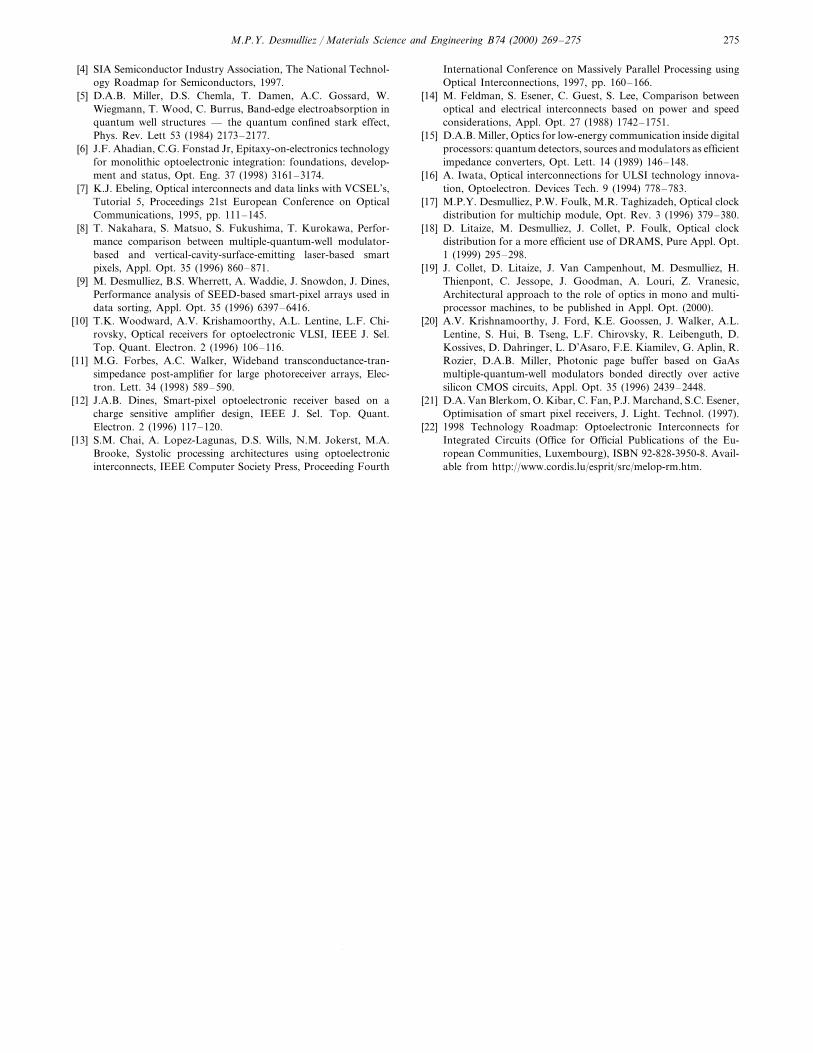
Table 7 provides a comparison of the drawbacks ofVCSEL-based and modulator-based systems. Two maindrawbacks in modulator based systems is the need foran external laser source to read the devices and thenecessity to have large voltage swing in order to drivethem. On the other hand, VCSEL-based demonstratorshave yet to show fully operational arrays of more than64 devices, all running at several GHz.
6. Assembly and testing issues
The high-aggregate bandwidth of such systems isuseful only if the data to be processed can be fed intothe system and be output on a timescale comparablewith the processing time of the demonstrators. In thecase of optical input and/or output data beams, the
M.P.Y. Desmulliez / Materials Science and Engineering B74 (2000) 269–275274
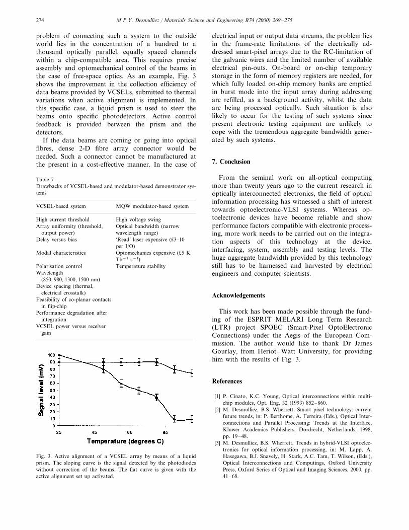
problem of connecting such a system to the outsideworld lies in the concentration of a hundred to athousand optically parallel, equally spaced channelswithin a chip-compatible area. This requires preciseassembly and optomechanical control of the beams inthe case of free-space optics. As an example, Fig. 3shows the improvement in the collection efficiency ofdata beams provided by VCSELs, submitted to thermalvariations when active alignment is implemented. Inthis specific case, a liquid prism is used to steer thebeams onto specific photodetectors. Active controlfeedback is provided between the prism and thedetectors.
If the data beams are coming or going into opticalfibres, dense 2-D fibre array connector would beneeded. Such a connector cannot be manufactured atthe present in a cost-effective manner. In the case of
electrical input or output data streams, the problem liesin the frame-rate limitations of the electrically ad-dressed smart-pixel arrays due to the RC-limitation ofthe galvanic wires and the limited number of availableelectrical pin-outs. On-board or on-chip temporarystorage in the form of memory registers are needed, forwhich fully loaded on-chip memory banks are emptiedin burst mode into the input array during addressingare refilled, as a background activity, whilst the dataare being processed optically. Such situation is alsolikely to occur for the testing of such systems sincepresent electronic testing equipment are unlikely tocope with the tremendous aggregate bandwidth gener-ated by such systems.
7. Conclusion
From the seminal work on all-optical computingmore than twenty years ago to the current research inoptically interconnected electronics, the field of opticalinformation processing has witnessed a shift of interesttowards optoelectronic-VLSI systems. Whereas op-toelectronic devices have become reliable and showperformance factors compatible with electronic process-ing, more work needs to be carried out on the integra-tion aspects of this technology at the device,interfacing, system, assembly and testing levels. Thehuge aggregate bandwidth provided by this technologystill has to be harnessed and harvested by electricalengineers and computer scientists.
Acknowledgements
This work has been made possible through the fund-ing of the ESPRIT MELARI Long Term Research(LTR) project SPOEC (Smart-Pixel OptoElectronicConnections) under the Aegis of the European Com-mission. The author would like to thank Dr JamesGourlay, from Heriot–Watt University, for providinghim with the results of Fig. 3.
References
[1] P. Cinato, K.C. Young, Optical interconnections within multi-chip modules, Opt. Eng. 32 (1993) 852–860.
[2] M. Desmulliez, B.S. Wherrett, Smart pixel technology: currentfuture trends, in: P. Berthome, A. Ferreira (Eds.), Optical Inter-connections and Parallel Processing: Trends at the Interface,Kluwer Academics Publishers, Dordrecht, Netherlands, 1998,pp. 19–48.
[3] M. Desmulliez, B.S. Wherrett, Trends in hybrid-VLSI optoelec-tronics for optical information processing, in: M. Lapp, A.Hasegawa, B.J. Snavely, H. Stark, A.C. Tam, T. Wilson, (Eds.),Optical Interconnections and Computings, Oxford UniversityPress, Oxford Series of Optical and Imaging Sciences, 2000, pp.41–68.
Table 7Drawbacks of VCSEL-based and modulator-based demonstrator sys-tems
MQW modulator-based systemVCSEL-based system
High voltage swingHigh current thresholdArray uniformity (threshold, Optical bandwidth (narrow
output power) wavelength range)‘Read’ laser expensive (£3–10Delay versus biasper I/O)Optomechanics expensive (£5 KModal characteristicsTb−1 s−1)
Polarisation control Temperature stabilityWavelength
(850, 980, 1300, 1500 nm)Device spacing (thermal,
electrical crosstalk)Feasibility of co-planar contacts
in flip-chipPerformance degradation after
integrationVCSEL power versus receiver
gain
Fig. 3. Active alignment of a VCSEL array by means of a liquidprism. The sloping curve is the signal detected by the photodiodeswithout correction of the beams. The flat curve is given with theactive alignment set up activated.
M.P.Y. Desmulliez / Materials Science and Engineering B74 (2000) 269–275 275
[4] SIA Semiconductor Industry Association, The National Technol-ogy Roadmap for Semiconductors, 1997.
[5] D.A.B. Miller, D.S. Chemla, T. Damen, A.C. Gossard, W.Wiegmann, T. Wood, C. Burrus, Band-edge electroabsorption inquantum well structures — the quantum confined stark effect,Phys. Rev. Lett 53 (1984) 2173–2177.
[6] J.F. Ahadian, C.G. Fonstad Jr, Epitaxy-on-electronics technologyfor monolithic optoelectronic integration: foundations, develop-ment and status, Opt. Eng. 37 (1998) 3161–3174.
[7] K.J. Ebeling, Optical interconnects and data links with VCSEL’s,Tutorial 5, Proceedings 21st European Conference on OpticalCommunications, 1995, pp. 111–145.
[8] T. Nakahara, S. Matsuo, S. Fukushima, T. Kurokawa, Perfor-mance comparison between multiple-quantum-well modulator-based and vertical-cavity-surface-emitting laser-based smartpixels, Appl. Opt. 35 (1996) 860–871.
[9] M. Desmulliez, B.S. Wherrett, A. Waddie, J. Snowdon, J. Dines,Performance analysis of SEED-based smart-pixel arrays used indata sorting, Appl. Opt. 35 (1996) 6397–6416.
[10] T.K. Woodward, A.V. Krishamoorthy, A.L. Lentine, L.F. Chi-rovsky, Optical receivers for optoelectronic VLSI, IEEE J. Sel.Top. Quant. Electron. 2 (1996) 106–116.
[11] M.G. Forbes, A.C. Walker, Wideband transconductance-tran-simpedance post-amplifier for large photoreceiver arrays, Elec-tron. Lett. 34 (1998) 589–590.
[12] J.A.B. Dines, Smart-pixel optoelectronic receiver based on acharge sensitive amplifier design, IEEE J. Sel. Top. Quant.Electron. 2 (1996) 117–120.
[13] S.M. Chai, A. Lopez-Lagunas, D.S. Wills, N.M. Jokerst, M.A.Brooke, Systolic processing architectures using optoelectronicinterconnects, IEEE Computer Society Press, Proceeding Fourth
International Conference on Massively Parallel Processing usingOptical Interconnections, 1997, pp. 160–166.
[14] M. Feldman, S. Esener, C. Guest, S. Lee, Comparison betweenoptical and electrical interconnects based on power and speedconsiderations, Appl. Opt. 27 (1988) 1742–1751.
[15] D.A.B. Miller, Optics for low-energy communication inside digitalprocessors: quantum detectors, sources and modulators as efficientimpedance converters, Opt. Lett. 14 (1989) 146–148.
[16] A. Iwata, Optical interconnections for ULSI technology innova-tion, Optoelectron. Devices Tech. 9 (1994) 778–783.
[17] M.P.Y. Desmulliez, P.W. Foulk, M.R. Taghizadeh, Optical clockdistribution for multichip module, Opt. Rev. 3 (1996) 379–380.
[18] D. Litaize, M. Desmulliez, J. Collet, P. Foulk, Optical clockdistribution for a more efficient use of DRAMS, Pure Appl. Opt.1 (1999) 295–298.
[19] J. Collet, D. Litaize, J. Van Campenhout, M. Desmulliez, H.Thienpont, C. Jessope, J. Goodman, A. Louri, Z. Vranesic,Architectural approach to the role of optics in mono and multi-processor machines, to be published in Appl. Opt. (2000).
[20] A.V. Krishnamoorthy, J. Ford, K.E. Goossen, J. Walker, A.L.Lentine, S. Hui, B. Tseng, L.F. Chirovsky, R. Leibenguth, D.Kossives, D. Dahringer, L. D’Asaro, F.E. Kiamilev, G. Aplin, R.Rozier, D.A.B. Miller, Photonic page buffer based on GaAsmultiple-quantum-well modulators bonded directly over activesilicon CMOS circuits, Appl. Opt. 35 (1996) 2439–2448.
[21] D.A. Van Blerkom, O. Kibar, C. Fan, P.J. Marchand, S.C. Esener,Optimisation of smart pixel receivers, J. Light. Technol. (1997).
[22] 1998 Technology Roadmap: Optoelectronic Interconnects forIntegrated Circuits (Office for Official Publications of the Eu-ropean Communities, Luxembourg), ISBN 92-828-3950-8. Avail-able from http://www.cordis.lu/esprit/src/melop-rm.htm.
.