Embed Size (px)
Citation preview
arX
iv:1
006.
4854
v1 [
cond
-mat
.mtr
l-sc
i] 2
4 Ju
n 20
10
Graphene Photonics and Optoelectronics
F. Bonaccorso, Z. Sun, T. Hasan, A. C. Ferrari∗
Department of Engineering, University of Cambridge, Cambridge CB3 0FA, UK
The richness of optical and electronic properties of graphene attracts enormous interest. Graphenehas high mobility and optical transparency, in addition to flexibility, robustness and environmentalstability. So far, the main focus has been on fundamental physics and electronic devices. However,we believe its true potential to be in photonics and optoelectronics, where the combination of itsunique optical and electronic properties can be fully exploited, even in the absence of a bandgap, andthe linear dispersion of the Dirac electrons enables ultra-wide-band tunability. The rise of graphenein photonics and optoelectronics is shown by several recent results, ranging from solar cells and lightemitting devices, to touch screens, photodetectors and ultrafast lasers. Here we review the state ofthe art in this emerging field.
I. INTRODUCTION
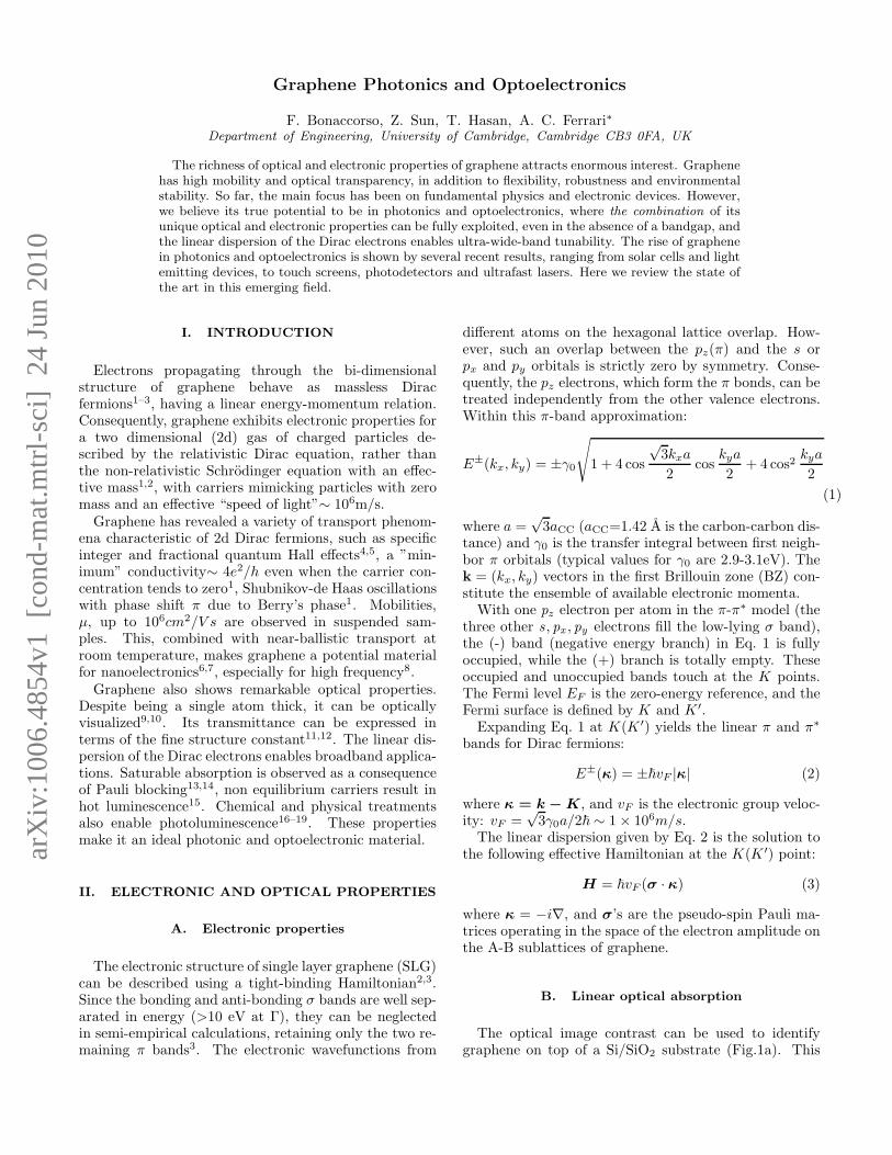
Electrons propagating through the bi-dimensionalstructure of graphene behave as massless Diracfermions1–3, having a linear energy-momentum relation.Consequently, graphene exhibits electronic properties fora two dimensional (2d) gas of charged particles de-scribed by the relativistic Dirac equation, rather thanthe non-relativistic Schrodinger equation with an effec-tive mass1,2, with carriers mimicking particles with zeromass and an effective “speed of light”∼ 106m/s.Graphene has revealed a variety of transport phenom-
ena characteristic of 2d Dirac fermions, such as specificinteger and fractional quantum Hall effects4,5, a ”min-imum” conductivity∼ 4e2/h even when the carrier con-centration tends to zero1, Shubnikov-de Haas oscillationswith phase shift π due to Berry’s phase1. Mobilities,µ, up to 106cm2/V s are observed in suspended sam-ples. This, combined with near-ballistic transport atroom temperature, makes graphene a potential materialfor nanoelectronics6,7, especially for high frequency8.Graphene also shows remarkable optical properties.
Despite being a single atom thick, it can be opticallyvisualized9,10. Its transmittance can be expressed interms of the fine structure constant11,12. The linear dis-persion of the Dirac electrons enables broadband applica-tions. Saturable absorption is observed as a consequenceof Pauli blocking13,14, non equilibrium carriers result inhot luminescence15. Chemical and physical treatmentsalso enable photoluminescence16–19. These propertiesmake it an ideal photonic and optoelectronic material.
II. ELECTRONIC AND OPTICAL PROPERTIES
A. Electronic properties
The electronic structure of single layer graphene (SLG)can be described using a tight-binding Hamiltonian2,3.Since the bonding and anti-bonding σ bands are well sep-arated in energy (>10 eV at Γ), they can be neglectedin semi-empirical calculations, retaining only the two re-maining π bands3. The electronic wavefunctions from
different atoms on the hexagonal lattice overlap. How-ever, such an overlap between the pz(π) and the s orpx and py orbitals is strictly zero by symmetry. Conse-quently, the pz electrons, which form the π bonds, can betreated independently from the other valence electrons.Within this π-band approximation:
E±(kx, ky) = ±γ0
√
1 + 4 cos
√3kxa
2cos
kya
2+ 4 cos2
kya
2
(1)
where a =√3aCC (aCC=1.42 A is the carbon-carbon dis-
tance) and γ0 is the transfer integral between first neigh-bor π orbitals (typical values for γ0 are 2.9-3.1eV). Thek = (kx, ky) vectors in the first Brillouin zone (BZ) con-stitute the ensemble of available electronic momenta.With one pz electron per atom in the π-π∗ model (the
three other s , px , py electrons fill the low-lying σ band),the (-) band (negative energy branch) in Eq. 1 is fullyoccupied, while the (+) branch is totally empty. Theseoccupied and unoccupied bands touch at the K points.The Fermi level EF is the zero-energy reference, and theFermi surface is defined by K and K ′.Expanding Eq. 1 at K(K ′) yields the linear π and π∗
bands for Dirac fermions:
E±(κ) = ±~vF |κ| (2)
where κ = k − K, and vF is the electronic group veloc-ity: vF =
√3γ0a/2~ ∼ 1× 10⁶m/s.
The linear dispersion given by Eq. 2 is the solution tothe following effective Hamiltonian at the K(K ′) point:
H = ~vF (σ · κ) (3)
where κ = −i∇, and σ’s are the pseudo-spin Pauli ma-trices operating in the space of the electron amplitude onthe A-B sublattices of graphene.
B. Linear optical absorption
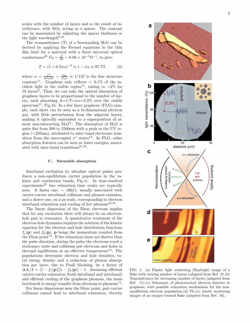
The optical image contrast can be used to identifygraphene on top of a Si/SiO2 substrate (Fig.1a). This
2
scales with the number of layers and is the result of in-terference, with SiO2 acting as a spacer. The contrastcan be maximized by adjusting the spacer thickness orthe light wavelength9,10.The transmittance (T) of a freestanding SLG can be
derived by applying the Fresnel equations in the thinfilm limit for a material with a fixed universal optical
conductance20 G0 = e2
4~∼ 6.08× 10⁻⁵Ω−1, to give:
T = (1 + 0.5πα)−2 ≈ 1− πα ≈ 97.7% (4)
where α = e2
4πǫ0~c= G0
πǫ0c≈ 1/137 is the fine structure
constant11. Graphene only reflects < 0.1% of the in-cident light in the visible region11, raising to ∼2% for10 layers9. Thus, we can take the optical absorption ofgraphene layers to be proportional to the number of lay-ers, each absorbing A=1-T=πα=2.3% over the visiblespectrum11, Fig.1b. In a few layer graphene (FLG) sam-ple, each sheet can be seen as a bi-dimensional electrongas, with little perturbation from the adjacent layers,making it optically equivalent to a superposition of al-most non-interacting SLG9. The absorption of SLG isquite flat from 300 to 2500nm with a peak in the UV re-gion (∼250nm), attributed to inter-band electronic tran-sition from the unoccupied π∗ states12. In FLG, otherabsorption features can be seen at lower energies, associ-ated with inter-band transitions21,22.
C. Saturable absorption
Interband excitation by ultrafast optical pulses pro-duces a non-equilibrium carrier population in the va-lence and conduction bands, Fig.1c. In time-resolvedexperiments23 two relaxation time scales are typicallyseen. A faster one, ∼ 100fs, usually associated withcarrier-carrier intraband collisions and phonon emission,and a slower one, on a ps scale, corresponding to electroninterband relaxation and cooling of hot phonons24,25.The linear dispersion of the Dirac electrons implies
that for any excitation there will always be an electron-hole pair in resonance. A quantitative treatment of theelectron-hole dynamics requires the solution of the kineticequation for the electron and hole distribution functionsfe(p) and fh(p), p being the momentum counted fromthe Dirac point14. If the relaxation times are shorter thanthe pulse duration, during the pulse the electrons reach astationary state and collisions put electrons and holes inthermal equilibrium at an effective temperature14. Thepopulations determine electron and hole densities, to-tal energy density and a reduction of photon absorp-tion per layer, due to Pauli blocking, by a factor of∆A/A = [1 − fe(p)][1 − fh(p)] − 1. Assuming efficientcarrier-carrier relaxation (both intraband and interband)and efficient cooling of the graphene phonons, the mainbottleneck is energy transfer from electrons to phonons14.For linear dispersions near the Dirac point, pair carrier
collisions cannot lead to interband relaxation, thereby
FIG. 1: (a) Elastic light scattering (Rayleigh) image of aflake with varying number of layers (adapted from Ref. 9).(b)Transmittance for increasing number of layers (adapted fromRef. 11).(c) Schematic of photoexcited electron kinetics ingraphene, with possible relaxation mechanisms for the non-equilibrium electron population.(d) PL;(e) elastic scatteringimages of an oxygen treated flake (adapted from Ref. 16).
3
conserving the total number of electrons and holesseparately14,26. Interband relaxation by phonon emis-sion can occur only if the electron and hole energiesare close to the Dirac point (within the phonon en-ergy). Non-equilibrium electron-hole recombination isalso possible15. For graphite flakes the situation is dif-ferent: the dispersion is quadratic, and pair carrier col-lisions can lead to interband relaxation. Thus, in prin-ciple, decoupled SLG can provide the highest saturableabsorption for a given amount of material14.
D. Luminescence
Graphene could be made luminescent by inducing aband gap, following two main routes. One is by cuttingit into ribbons and quantum dots, the other is by chemi-cal or physical treatments, to reduce the connectivity ofthe π electrons network. Even though graphene nanorib-bons (GNRs) have been produced, with varying bandgaps7, to date no photoluminescence (PL) has been re-ported from them. However, bulk graphene oxide (GO)dispersions and solids do show a broad PL17–19,27. Indi-vidual graphene flakes can be made brightly luminescentby mild oxygen plasma treatment16. The resulting PL isuniform across large areas, as shown in Figs. 1d,e, wherea PL map and the corresponding elastic scattering imageare compared. It is possible to make hybrid structures byetching just the top layer, while leaving underlying layersintact16. This combination of photoluminescent and con-ductive layers could be used in sandwich light-emittingdiodes. Luminescent graphene-based materials can nowbe routinely produced covering the infrared (IR), visibleand blue spectral range16–19,27.Even though some groups assigned PL in GO to band-
gap emission from electron confined sp2 islands17–19, thisis more likely to arise from oxygen related defect states16.Whatever the origin, fluorescent organic compounds areof significant importance to the development of low-costopto-electronic devices28. Blue PL from aromatic orolefinic molecules is particularly important for displayand lighting applications29. Luminescent quantum dotsare widely used for bio-labeling and bio-imaging. How-ever, their toxicity and potential environmental hazardlimit widespread use and in-vivo applications. Fluores-cent bio-compatible carbon-based nanomaterials, may bea more suitable alternative. Fluorescent species in the IRand near-IR are useful for biological applications sincecells and tissues exhibit little auto-fluorescence in thisregion30. Ref. 18 exploited PL GO for live cell imagingin the near-infrared with little background.Ref. 21 reported a gate-controlled, tunable gap up to
250meV in BLG. This may enable novel photonic devicesfor far IR light generation, amplification and detection.Broadband non-linear PL is also possible following non
equilibrium excitation of untreated graphene layers, Fig1c, as recently reported by several groups15. Emissionwas observed throughout the visible spectrum, for ener-
gies both higher and lower than the exciting one, in con-trast to conventional PL processes15. This broadbandnon linear-PL arises from recombination of a distribu-tion of non-equilibrium electrons and holes, generated byrapid scattering between photo-excited carriers after op-tical excitation15. It scales with the number of layers andcan be used as a quantitative imaging tool, as well as toreveal the hot electron-hole plasma dynamics15, Fig 1c.Electroluminescence was also recently reported in pris-
tine graphene31. Although the power conversion effi-ciency is lower than carbon nanotubes (CNTs), this couldlead to novel emitting devices based entirely on graphene.
III. PRODUCTION
Graphene was first produced by micromechanical ex-foliation of graphite32. This still gives the best samplesin terms of purity, defects, mobility and optoelectronicsproperties. However, large scale assembly is needed forthe widespread application of this material. Several tech-niques have been developed to provide a steady supply ofgraphene in large areas and quantities, amenable for massapplications. These comprise growth by chemical vapordeposition33–37, segregation by heat treatment of carboncontaining substrates38–40, liquid phase exfoliation41–45.In fact, most of these methods date back several decades.The current interest in graphene pushed these early ap-proaches to large yields, controlled growth, large areas,and enabled in just 6 years to go from micrometer flakesto near mass production of layer controlled samples.
A. Micromechanical cleavage
Micromechanical cleavage (MC)32 consists in peelingoff a piece of graphite by means of an adhesive tape. MChas been optimized to give SLG up to mm in size, of highstructural and electronic quality. Although this is themethod of choice for fundamental research, and most keyresults on individual SLG were obtained on MC flakes, ithas disadvantages in terms of yield and throughput, andis impractical for large scale applications.
B. Liquid phase exfoliation
Liquid phase exfoliation (LPE) of graphite consists inchemical wet dispersion followed by ultrasonication, bothin aqueous43 and non-aqueous solvents42. Up to∼ 70%SLG can be achieved by mild sonication in water withsodium deoxycholate followed by sedimentation based-ultracentrifugation46.Bile salts surfactants also allow the isolation of flakes
with controlled thickness, when combined with den-sity gradient ultracentrifugation (DGU)47. Exfoliationof graphite intercalated compounds44 and expandablegraphite48 was also reported.
4
LPE can also give GNRs with widths<10nm41 and of-fers advantages of scalability and no requirement of ex-pensive growth substrates. Furthermore it is an idealmeans to produce films and composites.
1. Graphene oxide
LPE of graphite was first obtained through sonica-tion of graphite oxide45, following the 60 years old Hum-mers method49, to produce graphene oxide (GO). Theoxidation of graphite in the presence of acids and oxi-dants, proposed already in the nineteenth century50,51,disrupts the sp2-network and introduces hydroxyl orepoxide groups52,53 with carboxylic or carbonyl groupsattached to the edges. These make GO sheets read-ily dispersible in water and several other solvents. Al-though large GO flakes can be produced, these are in-trinsically defective, and electrically insulating. Despiteseveral attempts45,52, reduced GO (RGO) does not fullyregain the pristine graphene electrical conductivity52,54.It is thus important to distinguish between dispersionprocessed graphene flakes, retaining the electronic prop-erties of graphene, and insulating GO layers.
C. Chemical vapor deposition
FLGs were grown more than 40 years ago by Chemi-cal Vapor Deposition (CVD)33. SLG and FLG can nowbe produced on various substrates by feeding hydrocar-bons at a suitable temperature33–37,55–57. The scale ofprogress in CVD growth is given by Ref. 37, where sam-ples over 60cm were achieved. Plasma-enhanced CVDcan be applied on substrates without catalyst57. Notethat most as-grown CVD samples are multilayer. Evenif their Raman spectrum appears similar35,36 to the idealSLG one58, this is just an indication of electronic decou-pling of the layers, not a definite proof of SLG growth.
D. Carbon segregation
Carbon segregation from silicon carbide38,59,60 ormetal substrates39,55,61–65, following high temperatureannealing, can produce graphene. As early as 1896 E.G. Acheson reported a method to produce graphite fromSiC59, while the segregation of graphene from Ni(111)was investigated over 30 years ago61. High quality layerscan now be produced on SiC in an Ar atmosphere40 andelectronic decoupling from the underlying SiC substratecan be achieved by H treatment66.
E. Chemical synthesis
Graphene or carbon nanosheets can also be chemicallysynthesized67. Total organic synthesis yields graphene-
like poly-aromatic hydrocarbons (PAHs)68. These syn-thetic nanographenes (NGs) can then be assembled toform larger layers. Supramolecular interactions can beused to cover SLG with PAHs, keeping the sp2 networkintact, without compromising the transport properties.NGs form ordered layers, with precise control of orien-tation and spacing69. These interact with the graphenebackbone allowing in principle to control and tune itsoptoelectronic properties69.
F. Deterministic placement
A fundamental step to produce useful devices is thedeterministic placement of graphene on pre-defined po-sitions on a substrate of choice. Transfer processesare common in the semiconductor industry. Extensiveexperience of transfer was developed for carbon nan-otubes (CNTs). Ref. 70 reported transfer of SLGand FLG from SiO2/Si to other substrates. A layerof poly(methyl methacrylate) (PMMA) was coated ongraphene deposited on SiO2, subsequently detached bypartial SiO2 etch70. The PMMA/graphene membranewas then placed over the target substrate and PMMAdissolved with acetone70. Ref. 35 used a dry-methodbased on a polydimethylsiloxane (PDMS) stamp to trans-fer patterned films. Ref. 37 scaled the process to a roll-based layer-by-layer transfer onto plastic substrates.We developed a procedure for deterministic placement,
following transfer. This exploits a water layer betweenthe PMMA/graphene foil and the substrate, enabling thePMMA to move. This allows to place graphene layers onany substrate in any predefined location, prepare ”artifi-cial” multi-layers, create sandwich structures with othermaterials (such as BN, MoS2), etc. We will show anexample of this technique in Section IVG, by placinggraphene on the core of an optical fibre.Large scale placement of LPE samples can be achieved
by spin coating and Langmuir-Blogdett48, even thoughwith lack of positional control. Surface modificationby self-assembled monolayers (SAMs) can enable tar-geted deposition of graphene flakes in a large scale. Di-electrophoresis allows controlled placement of individ-ual graphene flakes between pre-patterned electrodes71.Inkjet printing is another attractive technique72, andcould directly ”write” optoelectronic devices.
IV. PHOTONICS AND OPTOELECTRONICS
APPLICATIONS
A. Transparent conductors
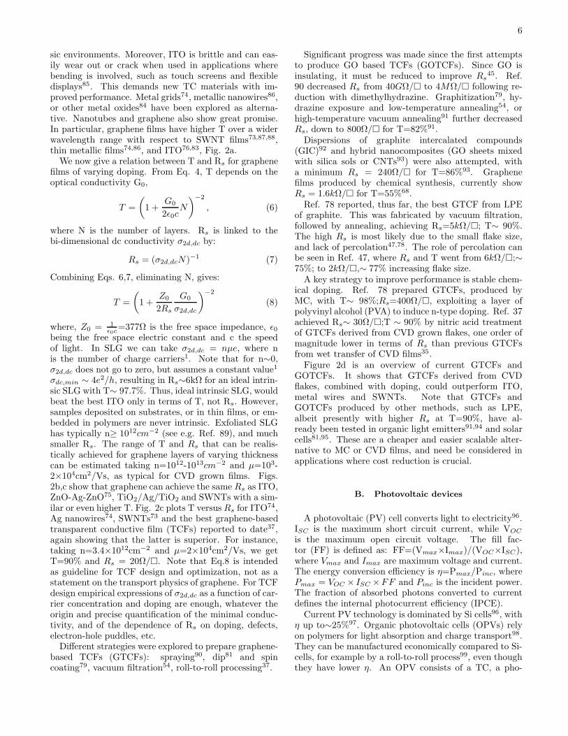
Optoelectronic devices such as displays, touch-screens,light emitting diodes, solar cells, require materials withlow sheet resistance Rs and high transparency. In a thin-film Rs = ρ/d, where d is the film thickness and ρ =1/σdc the resistivity. For a rectangle of length L and
5
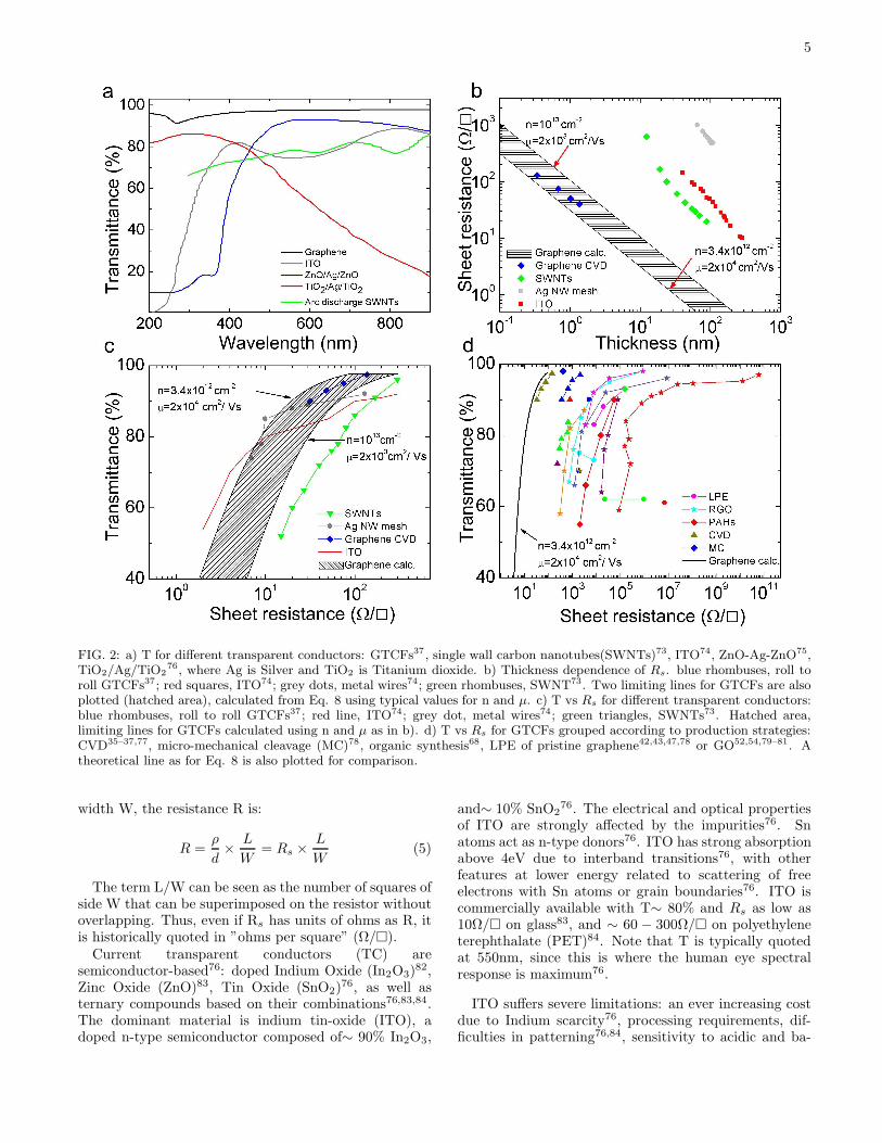
FIG. 2: a) T for different transparent conductors: GTCFs37 , single wall carbon nanotubes(SWNTs)73, ITO74, ZnO-Ag-ZnO75,TiO2/Ag/TiO2
76, where Ag is Silver and TiO2 is Titanium dioxide. b) Thickness dependence of Rs. blue rhombuses, roll toroll GTCFs37; red squares, ITO74; grey dots, metal wires74; green rhombuses, SWNT73. Two limiting lines for GTCFs are alsoplotted (hatched area), calculated from Eq. 8 using typical values for n and µ. c) T vs Rs for different transparent conductors:blue rhombuses, roll to roll GTCFs37 ; red line, ITO74; grey dot, metal wires74; green triangles, SWNTs73. Hatched area,limiting lines for GTCFs calculated using n and µ as in b). d) T vs Rs for GTCFs grouped according to production strategies:CVD35–37,77, micro-mechanical cleavage (MC)78, organic synthesis68, LPE of pristine graphene42,43,47,78 or GO52,54,79–81. Atheoretical line as for Eq. 8 is also plotted for comparison.
width W, the resistance R is:
R =ρ
d× L
W= Rs ×
L
W(5)
The term L/W can be seen as the number of squares ofside W that can be superimposed on the resistor withoutoverlapping. Thus, even if Rs has units of ohms as R, itis historically quoted in ”ohms per square” (Ω/).Current transparent conductors (TC) are
semiconductor-based76: doped Indium Oxide (In2O3)82,
Zinc Oxide (ZnO)83, Tin Oxide (SnO2)76, as well as
ternary compounds based on their combinations76,83,84.The dominant material is indium tin-oxide (ITO), adoped n-type semiconductor composed of∼ 90% In2O3,
and∼ 10% SnO276. The electrical and optical properties
of ITO are strongly affected by the impurities76. Snatoms act as n-type donors76. ITO has strong absorptionabove 4eV due to interband transitions76, with otherfeatures at lower energy related to scattering of freeelectrons with Sn atoms or grain boundaries76. ITO iscommercially available with T∼ 80% and Rs as low as10Ω/ on glass83, and ∼ 60 − 300Ω/ on polyethyleneterephthalate (PET)84. Note that T is typically quotedat 550nm, since this is where the human eye spectralresponse is maximum76.
ITO suffers severe limitations: an ever increasing costdue to Indium scarcity76, processing requirements, dif-ficulties in patterning76,84, sensitivity to acidic and ba-
6
sic environments. Moreover, ITO is brittle and can eas-ily wear out or crack when used in applications wherebending is involved, such as touch screens and flexibledisplays85. This demands new TC materials with im-proved performance. Metal grids74, metallic nanowires86,or other metal oxides84 have been explored as alterna-tive. Nanotubes and graphene also show great promise.In particular, graphene films have higher T over a widerwavelength range with respect to SWNT films73,87,88,thin metallic films74,86, and ITO76,83, Fig. 2a.We now give a relation between T and Rs for graphene
films of varying doping. From Eq. 4, T depends on theoptical conductivity G0,
T =
(
1 +G0
2ǫ0cN
)−2
, (6)
where N is the number of layers. Rs is linked to thebi-dimensional dc conductivity σ2d,dc by:
Rs = (σ2d,dcN)−1 (7)
Combining Eqs. 6,7, eliminating N, gives:
T =
(
1 +Z0
2Rs
G0
σ2d,dc
)−2
(8)
where, Z0 = 1ǫ0c
=377Ω is the free space impedance, ǫ0being the free space electric constant and c the speedof light. In SLG we can take σ2d,dc = nµe, where nis the number of charge carriers1. Note that for n∼0,σ2d,dc does not go to zero, but assumes a constant value1
σdc,min ∼ 4e2/h, resulting in Rs∼6kΩ for an ideal intrin-sic SLG with T∼ 97.7%. Thus, ideal intrinsic SLG, wouldbeat the best ITO only in terms of T, not Rs. However,samples deposited on substrates, or in thin films, or em-bedded in polymers are never intrinsic. Exfoliated SLGhas typically n≥ 1012cm−2 (see e.g. Ref. 89), and muchsmaller Rs. The range of T and Rs that can be realis-tically achieved for graphene layers of varying thicknesscan be estimated taking n=1012-1013cm−2 and µ=103-2×104cm2/Vs, as typical for CVD grown films. Figs.2b,c show that graphene can achieve the same Rs as ITO,ZnO-Ag-ZnO75, TiO2/Ag/TiO2 and SWNTs with a sim-ilar or even higher T. Fig. 2c plots T versus Rs for ITO
74,Ag nanowires74, SWNTs73 and the best graphene-basedtransparent conductive film (TCFs) reported to date37,again showing that the latter is superior. For instance,taking n=3.4×1012cm−2 and µ=2×104cm2/Vs, we getT=90% and Rs = 20Ω/. Note that Eq.8 is intendedas guideline for TCF design and optimization, not as astatement on the transport physics of graphene. For TCFdesign empirical expressions of σ2d,dc as a function of car-rier concentration and doping are enough, whatever theorigin and precise quantification of the minimal conduc-tivity, and of the dependence of Rs on doping, defects,electron-hole puddles, etc.Different strategies were explored to prepare graphene-
based TCFs (GTCFs): spraying90, dip81 and spincoating79, vacuum filtration54, roll-to-roll processing37.
Significant progress was made since the first attemptsto produce GO based TCFs (GOTCFs). Since GO isinsulating, it must be reduced to improve Rs
45. Ref.90 decreased Rs from 40GΩ/ to 4MΩ/ following re-duction with dimethylhydrazine. Graphitization79, hy-drazine exposure and low-temperature annealing54, orhigh-temperature vacuum annealing91 further decreasedRs, down to 800Ω/ for T=82%91.Dispersions of graphite intercalated compounds
(GIC)92 and hybrid nanocomposites (GO sheets mixedwith silica sols or CNTs93) were also attempted, witha minimum Rs = 240Ω/ for T=86%93. Graphenefilms produced by chemical synthesis, currently showRs = 1.6kΩ/ for T=55%68.Ref. 78 reported, thus far, the best GTCF from LPE
of graphite. This was fabricated by vacuum filtration,followed by annealing, achieving Rs=5kΩ/; T∼ 90%.The high Rs is most likely due to the small flake size,and lack of percolation47,78. The role of percolation canbe seen in Ref. 47, where Rs and T went from 6kΩ/;∼75%; to 2kΩ/,∼ 77% increasing flake size.A key strategy to improve performance is stable chem-
ical doping. Ref. 78 prepared GTCFs, produced byMC, with T∼ 98%;Rs=400Ω/, exploiting a layer ofpolyvinyl alcohol (PVA) to induce n-type doping. Ref. 37achieved Rs∼ 30Ω/;T ∼ 90% by nitric acid treatmentof GTCFs derived from CVD grown flakes, one order ofmagnitude lower in terms of Rs than previous GTCFsfrom wet transfer of CVD films35.Figure 2d is an overview of current GTCFs and
GOTCFs. It shows that GTCFs derived from CVDflakes, combined with doping, could outperform ITO,metal wires and SWNTs. Note that GTCFs andGOTCFs produced by other methods, such as LPE,albeit presently with higher Rs at T=90%, have al-ready been tested in organic light emitters91,94 and solarcells81,95. These are a cheaper and easier scalable alter-native to MC or CVD films, and need be considered inapplications where cost reduction is crucial.
B. Photovoltaic devices
A photovoltaic (PV) cell converts light to electricity96.ISC is the maximum short circuit current, while VOC
is the maximum open circuit voltage. The fill fac-tor (FF) is defined as: FF=(Vmax×Imax)/(VOC×ISC),where Vmax and Imax are maximum voltage and current.The energy conversion efficiency is η=Pmax/Pinc, wherePmax = VOC × ISC ×FF and Pinc is the incident power.The fraction of absorbed photons converted to currentdefines the internal photocurrent efficiency (IPCE).Current PV technology is dominated by Si cells96, with
η up to∼25%97. Organic photovoltaic cells (OPVs) relyon polymers for light absorption and charge transport98.They can be manufactured economically compared to Si-cells, for example by a roll-to-roll process99, even thoughthey have lower η. An OPV consists of a TC, a pho-
7
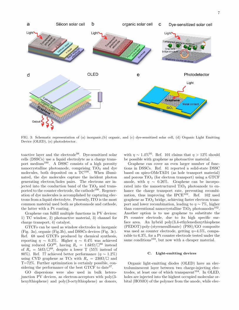
FIG. 3: Schematic representation of (a) inorganic,(b) organic, and (c) dye-sensitized solar cell, (d) Organic Light EmittingDevice (OLED), (e) photodetector.
toactive layer and the electrode98. Dye-sensitized solarcells (DSSCs) use a liquid electrolyte as a charge trans-port medium100. A DSSC consists of a high porositynanocrystalline photoanode, comprising TiO2 and dyemolecules, both deposited on a TC100. When illumi-nated, the dye molecules capture the incident photongenerating electron/holes pairs. The electrons are in-jected into the conduction band of the TiO2 and trans-ported to the counter electrode, the cathode100. Regener-ation of dye molecules is accomplished by capturing elec-trons from a liquid electrolyte. Presently, ITO is the mostcommon material used both as photoanode and cathode,the latter with a Pt coating.Graphene can fulfill multiple functions in PV devices:
1) TC window, 2) photoactive material, 3) channel forcharge transport, 4) catalyst.GTCFs can be used as window electrodes in inorganic
(Fig. 3a), organic (Fig.3b), and DSSCs devices (Fig. 3c).Ref. 68 used GTCFs produced by chemical synthesis,reporting η ∼ 0.3%. Higher η ∼ 0.4% was achievedusing reduced GO80, having Rs = 1.6kΩ/80 insteadof Rs = 5kΩ/68, despite a lower T (55% instead of80%). Ref. 77 achieved better performance (η ∼ 1.2%)using CVD graphene as TCs with Rs = 230Ω/ andT=72%. Further optimization is certainly possible, con-sidering the performance of the best GTCF to date37.GO dispersions were also used in bulk hetero-
junction PV devices, as electron-acceptors with poly(3-hexylthiophene) and poly(3-octylthiophene) as donors,
with η ∼ 1.4%95. Ref. 101 claims that η > 12% shouldbe possible with graphene as photoactive material.Graphene can cover an even larger number of func-
tions in DSSCs. Ref. 81 reported a solid-state DSSCbased on spiro-OMeTAD1 (as hole transport material)and porous TiO2 (for electron transport) using a GTCFanode, with η ∼ 0.26%. Graphene can be incorpo-rated into the nanostructured TiO2 photoanode to en-hance the charge transport rate, preventing recombi-nation, thus improving the IPCE102. Ref. 102 usedgraphene as TiO2 bridge, achieving faster electron trans-port and lower recombination, leading to η ∼ 7%, higherthan conventional nanocrystalline TiO2 photoanodes102.Another option is to use graphene to substitute thePt counter electrode, due to its high specific sur-face area. An hybrid poly(3,4-ethylenedioxythiophene(PEDOT):poly-(styrenesulfonate) (PSS)/GO compositewas used as counter electrode, getting η=4.5%, compa-rable to 6.3%, for a Pt counter electrode tested under thesame conditions103, but now with a cheaper material.
C. Light-emitting devices
Organic light-emitting diodes (OLED) have an elec-troluminescent layer between two charge-injecting elec-trodes, at least one of which transparent104. In OLED,holes are injected into the highest occupied molecular or-bital (HOMO) of the polymer from the anode, while elec-
8
trons are injected into the lowest unoccupied molecularorbital (LUMO) from the cathode. For efficiently injec-tion, the anode and cathode work functions should matchthe HOMO and LUMO of the light-emitting polymer104.Due to the image quality, low power consumption andultra-thin device structure, OLEDs find applications inultra-thin televisions and other display screens, such ascomputer monitors, digital cameras and mobile phones.Traditionally, ITO, having a work function 4.4-4.5eV, isused as TCF. However, besides cost issues, ITO is brittleand limited as flexible substrate84. Also, In tends to dif-fuse into the active OLED layers, leading to a reductionof performance over time76. Thus, there is a need for al-ternative TCFs with optical and electrical performancesimilar to ITO, but without its drawbacks. Graphene hasa work function of 4.5eV105, similar to ITO. This, com-bined with its promise as flexible and cheap TCF, makesit an ideal candidate as OLED anode, Fig. 3d, eliminat-ing at the same time the issues related to In diffusion.GTCFs anodes enabled out-coupling efficiency compara-ble to ITO91. Considering that Rs and T were 800Ω/and 82% at 550nm91, it is reasonable to expect furtheroptimization will improve performance.Ref. 94 used a GOTCF in a light-emitting electro-
chemical cell (LEC). This is a device, similar to anOLED, where the light-emitting polymer is blended withan electrolyte106. The mobile ions in the electrolyte rear-range when a potential is applied between the electrodes,forming high charge-density layers at each electrode in-terface, allowing efficient and balanced injection of elec-trons and holes, regardless of the work function of theelectrodes106. Usually, LECs have at least one metalelectrode. Electrochemical side-reactions, involving theelectrode materials, can cause problems in terms of oper-ational lifetime and efficiency94. This also hinders the de-velopment of flexible LEC devices. Graphene is the idealmaterial to overcome these problems. Ref. 94 demon-strated a LEC based solely on dispersion-processablecarbon-based materials, paving the way to totally organiclow-voltage, inexpensive, and efficient LEDs.
D. Photodetectors
Photodetectors (PDs) measure photon flux or opticalpower by converting the absorbed photon energy intoelectrical current. They are widely used in a rangeof common devices107, such as remote controls, TVs,DVD players, etc. Most PDs exploit the internal photo-effect, where the absorption of photons results in car-riers excited from the valence to the conduction band,outputting an electric current. The spectral bandwidthis typically limited by the material absorption107. Forexample, PDs based on IV and III-V semiconductorssuffer from the so-called ”long-wavelength limit”, asthese become transparent when the incident energy issmaller than the bandgap107. Graphene absorbs fromUV to THz11,14,108,109. As a result, graphene based PDs
(GPDs) (see Fig. 3e) could work over a much broaderwavelength range. The response time is ruled by the car-rier mobility107. Graphene has huge mobilities. Hence,GPDs can be ultrafast.The photoelectrical response of graphene has
been widely investigated, both experimentally andtheoretically110–114. Photoelectrical response at 0.514,0.633, 1.5 and 2.4µm was reported114. Much broaderspectral detection is expected due to the graphene ul-trawideband absorption. Ref. 113 demonstrated a GPDwith photo-response up to 40GHz. The GPD operationbandwidth is mainly limited by the time constant re-sulting from the device resistance R and capacitance C.Ref. 113, reported a RC limited bandwidth∼ 640GHz,comparable to traditional PDs115. However, the max-imum possible operation bandwidth of PDs is typicallyrestricted by the transit time, the finite duration of thephoto-generated current107. The transit time limitedbandwidth of a GPD could be well over 1500GHz113,surpassing state-of-the-art PDs.Although external electric field can produce efficient
photocurrent generation, with > 30% electron-hole sepa-ration efficiency111, zero source-drain bias and dark cur-rent operations could be achieved by using the internalelectric field formed near the metal electrode-grapheneinterfaces113,114. The small effective area of the internalelectric field could decrease the detection efficiency113,114,since most of the generated electron-hole pairs would beout of the electric field, thus recombining, rather than be-ing separated. The IPCE (15− 30%)111,112 and externalresponsivity (generated electric current for given inputoptical power) of 6.1mA/W114 so far reported for GPDsare relatively low compared to current PDs107. This ismainly due to limited optical absorption when only oneSLG is used, short photo-carrier lifetime, and small ef-fective photo-detection area (∼ 200nm in Ref. 113).The photo-thermoelectric effect, which exploits the
conversion of photon energy into heat and then elec-tric signal107, may play an important role in photocur-rent generation in graphene devices111,116. Thus photo-thermoelectric GPDs may be possible.
E. Touch screens
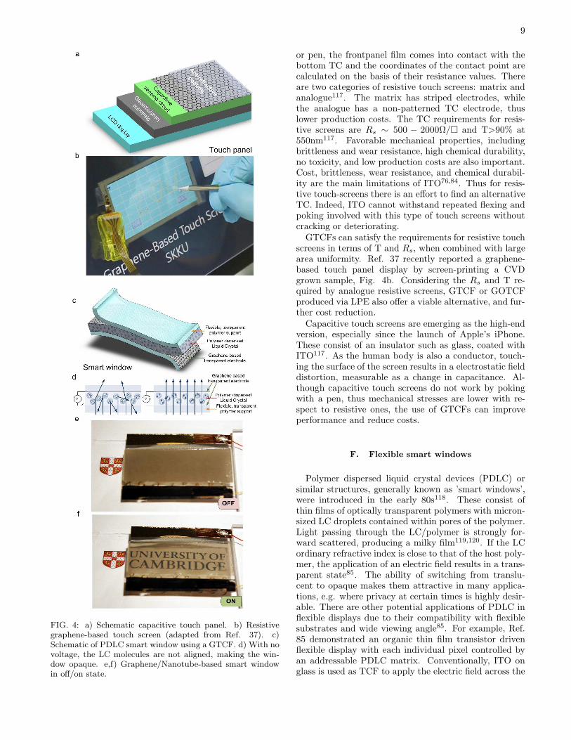
Touch screens are visual outputs that can detect thepresence and location of a touch, by a finger or otherobjects, such as a pen, within the display area, therebypermitting the physical interaction with what shown onthe display itself117. Touch panels are currently used ina wide range of applications, such as cellular phones anddigital cameras, and where keyboard and mouse do notallow a satisfactory, intuitive, quick, or accurate interac-tion by the user with the display content.Resistive and capacitive (see Fig. 4a) touch panels are
the most common. A resistive touch panel comprisesa conductive substrate, a liquid crystal device (LCD)frontpanel, and a TCF117. When pressed by a finger
9
FIG. 4: a) Schematic capacitive touch panel. b) Resistivegraphene-based touch screen (adapted from Ref. 37). c)Schematic of PDLC smart window using a GTCF. d) With novoltage, the LC molecules are not aligned, making the win-dow opaque. e,f) Graphene/Nanotube-based smart windowin off/on state.
or pen, the frontpanel film comes into contact with thebottom TC and the coordinates of the contact point arecalculated on the basis of their resistance values. Thereare two categories of resistive touch screens: matrix andanalogue117. The matrix has striped electrodes, whilethe analogue has a non-patterned TC electrode, thuslower production costs. The TC requirements for resis-tive screens are Rs ∼ 500 − 2000Ω/ and T>90% at550nm117. Favorable mechanical properties, includingbrittleness and wear resistance, high chemical durability,no toxicity, and low production costs are also important.Cost, brittleness, wear resistance, and chemical durabil-ity are the main limitations of ITO76,84. Thus for resis-tive touch-screens there is an effort to find an alternativeTC. Indeed, ITO cannot withstand repeated flexing andpoking involved with this type of touch screens withoutcracking or deteriorating.GTCFs can satisfy the requirements for resistive touch
screens in terms of T and Rs, when combined with largearea uniformity. Ref. 37 recently reported a graphene-based touch panel display by screen-printing a CVDgrown sample, Fig. 4b. Considering the Rs and T re-quired by analogue resistive screens, GTCF or GOTCFproduced via LPE also offer a viable alternative, and fur-ther cost reduction.Capacitive touch screens are emerging as the high-end
version, especially since the launch of Apple’s iPhone.These consist of an insulator such as glass, coated withITO117. As the human body is also a conductor, touch-ing the surface of the screen results in a electrostatic fielddistortion, measurable as a change in capacitance. Al-though capacitive touch screens do not work by pokingwith a pen, thus mechanical stresses are lower with re-spect to resistive ones, the use of GTCFs can improveperformance and reduce costs.
F. Flexible smart windows
Polymer dispersed liquid crystal devices (PDLC) orsimilar structures, generally known as ’smart windows’,were introduced in the early 80s118. These consist ofthin films of optically transparent polymers with micron-sized LC droplets contained within pores of the polymer.Light passing through the LC/polymer is strongly for-ward scattered, producing a milky film119,120. If the LCordinary refractive index is close to that of the host poly-mer, the application of an electric field results in a trans-parent state85. The ability of switching from translu-cent to opaque makes them attractive in many applica-tions, e.g. where privacy at certain times is highly desir-able. There are other potential applications of PDLC inflexible displays due to their compatibility with flexiblesubstrates and wide viewing angle85. For example, Ref.85 demonstrated an organic thin film transistor drivenflexible display with each individual pixel controlled byan addressable PDLC matrix. Conventionally, ITO onglass is used as TCF to apply the electric field across the
10
PDLC. However, one of the reasons behind the limitedmarket penetration of smart windows is the significantITO cost. Furthermore, flexibility is hindered when usingITO, reducing potential applications, such as PDLC flex-ible displays85. For transparent or colored/tinted smartwindows, the generally required T and Rs range from60 to 90% and above and 100 to 1kΩ/ depending onproduction cost, application and manufacturer. In addi-tion to flexibility, the electrodes need to be as large asthe window itself and must have long term physical andchemical stability, as well as being compatible with theroll to roll PDLC production process.All these deficiencies of ITO electrodes can be over-
come by GTCFs. Figures 4c,d shows the working princi-ple and Fig. 4e,f a prototype of a flexible smart windowwith PET used as substrate.
G. Saturable absorbers and ultrafast lasers
Materials with non-linear optical and electro-opticalproperties are needed in most photonic applications13,121.Laser sources producing nano- to sub-picosecond pulsesare a major component in the portfolio of leading lasermanufacturers. Thus far, solid-state lasers are the short-pulse source of choice, being deployed in a variety of ap-plications ranging from basic research to material pro-cessing, from eye surgery to printed circuit board man-ufacturing, from metrology to trimming of electroniccomponents such as resistors and capacitors. Regard-less of wavelength, the majority of ultrafast laser sys-tems employ a mode-locking technique, whereby a non-linear optical element, called saturable absorber (SA),turns the continuous wave output into a train of ultrafastoptical pulses122. The key requirements for non-linearmaterials are fast response time, strong non-linearity,broad wavelength range, low optical loss, high power han-dling, low power consumption, low cost and ease of in-tegration into an optical system. Currently, the domi-nant technology is based on semiconductor saturable ab-sorber mirrors (SESAMs)122. However, these have a nar-row tuning range, and require complex fabrication andpackaging13,122. A simple, cost-effective alternative isto use SWNTs13,123, where the diameter controls thegap, thus the operating wavelength. Broadband tun-ability is possible using SWNTs with a wide diameterdistribution13,123. However, when operating at a partic-ular wavelength, SWNTs not in resonance are not usedand contribute unwanted losses.As discussed in Sect.II C, the linear dispersion of the
Dirac electrons in graphene offers an ideal solution: forany excitation there is always an electron-hole pair in res-onance. The ultrafast carrier dynamics23,124, combinedwith large absorption and Pauli blocking make graphenean ideal ultra-broadband, fast SA. Compared to SESAMsand SWNTs, there is no need of bandgap engineering orchirality/diameter control.Thus far, graphene-polymer composites13,14,125–127,
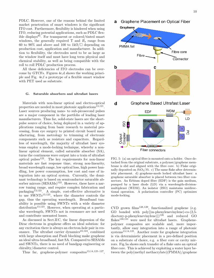
FIG. 5: (a) an optical fibre is mounted onto a holder. Once de-tached from the original substrate, a polymer/graphene mem-brane is slid and aligned with the fibre core. b) Flake origi-nally deposited on SiO2/Si. c) The same flake after determin-istic placement. d) graphene-mode locked ultrafast laser: agraphene saturable absorber is placed between two fiber con-nectors. An Erbium doped fibre (EDF) is the gain medium,pumped by a laser diode (LD) via a wavelength-division-multiplexer (WDM). An isolator (ISO) maintains unidirec-tional operation. A polarization controller (PC) optimizesmode-locking.
CVD grown films128,129, functionalized graphene (e.g.GO bonded with poly[(m-phenylenevinylene)-co-(2,5-dioctoxy-p-phenylenevinylene)])126 and reduced GOflakes130,131 were used for ultrafast lasers. Graphene-polymer composites are scalable and, more impor-tantly, allow easy integration into a range of photonicsystems13,14,125. Another route for graphene integrationis via deterministic placement in a pre-defined positionon a substrate of choice, e.g. a fiber core or cavity mir-rors. Fig.5a shows such transfer of a flake onto an opticalfibre core. This is achieved by exploiting a water layer be-tween the poly(methyl methacrylate)(PMMA)/graphene
11
FIG. 6: a) Absorption of graphene-PVA composite and reference PVA. Inset: micrograph of the composite.(b) Typical trans-mission as a function of pump power at six wavelengths. T increases with power.(c) Tuneable (>30nm) fiber laser mode-lockedby graphene. (d) Autocorrelation (AC) trace and (e) spectrum of output pulses of a GO-mode-locked laser, with a∼743fspulse duration. Table: GSA mode-locked laser performances.EDFL: Erbium-doped fiber laser; FG: Functionalized graphene;Nd:YAG SSL: Neodymium doped ytterbium aluminum garnet solid-state laser.
12
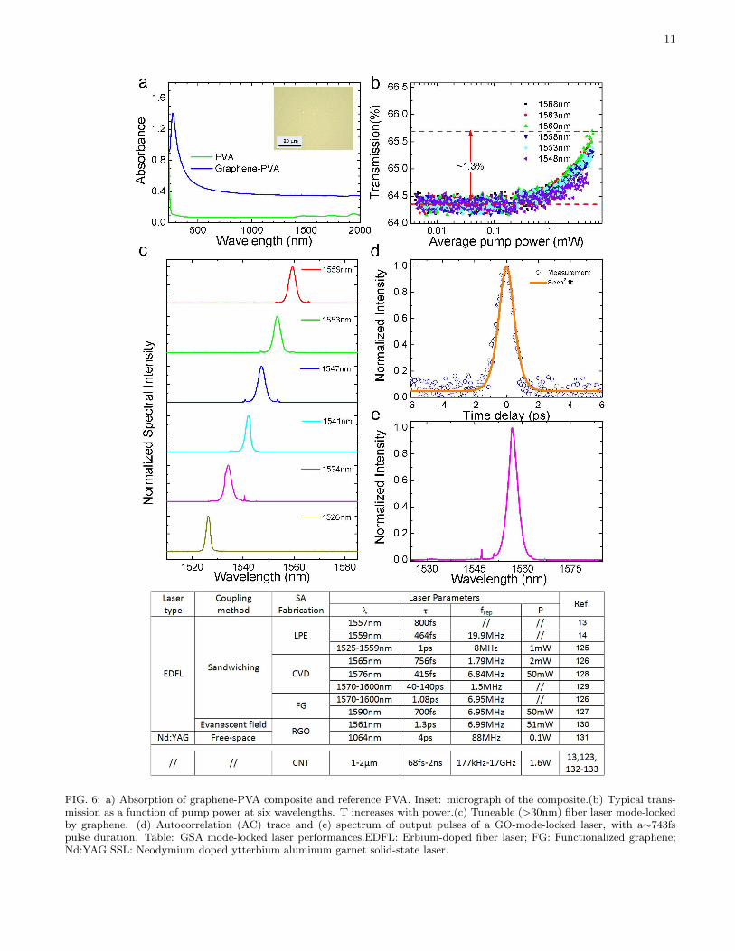
foil and the optical fibre, which enables the PMMA tomove. Graphene integration is finally obtained after pre-cise alignment to the fibre core by a micro-manipulator(Fig. 5 b) and dissolution of the PMMA layer (Fig.5c).A typical absorption spectrum is shown in
Fig.6a13,14,125. This is featureless, save a charac-teristic UV plasmon peak, while the host polymer onlycontributes a small background for longer wavelengths.Fig.6b plots T as a function of average pump power atsix wavelengths. Saturable absorption is evident by theT increase with power at all wavelengths.Various strategies have been proposed to integrate
graphene saturable absorbers (GSAs) in laser cavities forultrafast pulse generation. The most common is to sand-wich a GSA between two fibre connectors with a fibreadapter, as schematized in Fig.5c13,14,125. Graphene ona side-polished fiber was also reported, aimed at highpower generation by evanescent field interaction130. Aquartz substrate coated with graphene was used for free-space solid-state lasers131.The most common wavelength of generated ultrafast
pulses so far is∼ 1.5µm, since this is the standard in op-tical telecommunications, not because GSAs have anypreference for a particular wavelength. A solid-statelaser mode-locked by graphene was reported at∼ 1µm131.Fig.6c shows a GSA-mode locked EDF laser tuneablefrom 1526 to 1559nm125, with the tuning range mainlylimited by the tunable filter, not the GSA. Fig.6d,e showthe pulse from a GO based saturable absorber (GOSA).The possibility of tuning the GSA properties by function-alization and using different layers or composite concen-trations, offers considerable design freedom. Fig.6 has atable comparing the performance of graphene-based ul-trafast lasers and the main CNT-based devices132,133.
H. Optical limiters
Optical limiters (OL) are devices with high trans-mittance for low incident light intensity, and vice-versafor high intensity134. There is a great interest in OLmainly for optical sensors and human eye protection134,as damage can happen when the intensity exceeds athreshold134. Passive OL using a nonlinear optical ma-terial, have potential for simplicity, compactness and lowcost134. However, so far there is no demonstration ofpassive OL able to protect eyes and other common sen-sors over the entire visible and NIR range134. TypicalOL materials include semiconductors (e.g. ZnSe, InSb),organic molecules (e.g. phthalocyanines), LC and carbonbased composites (e.g. carbon-black dispersions, CNTs,fullerenes)134,135. Fullerenes and their derivatives136,137
and CNTs dispersions137 have good OL performance, inparticular for ns pulses at 532 and 1064nm137.In graphene-based OL the absorbed light energy con-
verts into heat, creating bubbles and microplasmas135,resulting in reduced transmission. Graphene dispersionscan be used as wideband OL covering visible and NIR.
Broad OL (from 532 to 1064nm) of LPE graphene wasreported for ns pulses135. It was shown that funtionalizedgraphene dispersions could outperform C60
138.
I. Optical Frequency converters
Optical frequency converters are used to expand thewavelength accessibility of lasers (e.g. frequency dou-bling, parametric amplification and oscillation, and four-wave mixing (FWM))134. Calculations suggest that non-linear frequency generation in graphene (e.g. harmonicsof input light) should be possible for sufficiently high ex-ternal electric field (> 100V/cm)139. Second harmonicgeneration (SHG) from a 150fs laser at 800nm was re-ported for a graphene film140. In addition, FWM, gen-erating NIR wavelength-tunable light was demonstratedusing SLG and FLG141. Graphene’s third-order suscep-tibility was measured to be |χ3| ∼ 10−7esu141, one orderof magnitude larger than reported so far for CNTs141.However, photon-counting electronics is typically neededto measure the output140, indicating a low conversionefficiency. Other features of graphene, such as the pos-sibility of tuning the nonlinearity by changing the num-ber of layers141, and wavelength-independent nonlinearsusceptibility141, still could be potentially used for vari-ous photonic applications (e.g. optical imaging141).
J. THz devices
THz radiation in the 0.3 to 10THz range (30µm to1mm), is attractive for biomedical imaging, security,remote sensing and spectroscopy142. A large amountof unexplored territory for THz technology still re-mains mainly due to a lack of affordable and effi-cient THz sources and detectors142. The frequency ofgraphene plasma waves143,144 lies in the THz range,as well as the gap of GNRs, and the BLG tunableband gap, making graphene appealing for THz gener-ation and detection. Various THz sources were sug-gested, based on electrical143,144 or optical143,144 pumpof graphene devices. Recent experimental observationsof THz emission145 and amplification146 in opticallypumped graphene show the feasibility of graphene-basedTHz generation. Twisted multilayers, retaining the elec-tronic properties of SLG, could also be interesting forTHz applications.
Graphene devices can be used for THz detection andfrequency conversion. The possibility of tuning the elec-tric and optical properties by external means (e.g. elec-tric and magnetic field, optical pump), makes SLG andFLG suitable for IR and THz radiation manipulation aswell. The possible devices include modulators, filters,switches, beam splitters and polarizers.
13
V. PERSPECTIVE
Graphene films and composites have attractive elec-tronic and optical properties, making them ideal for pho-tonics and optoelectronics. A number of applications areenabled by using graphene as a replacement for ITO andother transparent conductors. In many cases (e.g. touch-screens, OLEDs) this also adds fabrication flexibility, inaddition to economic advantages. Current PDLC-baseddevices face major challenges due to fabrication costs as-sociated with the requirement of large transparent elec-trodes. The move to a graphene-based technology couldmake them more viable. Novel graphene-based transpar-ent electrodes on flexible substrates for solar cells can addvalue and operational flexibility, not possible with cur-rent transparent conductors and rigid glass substrates.Recent progresses on growth and dispersion processingof graphene have definitely made this material ”come ofage”, encouraging industrial applications. Determinis-tic placement of graphene layers on arbitrary substrates,and multi-layers by individual assembly of monolayers atgiven angles are now possible. Future efforts on nonlin-ear optical devices will focus on demonstrators at dif-
ferent wavelengths to fully exploit graphene’s ultrawidebroadband capability. Ultrafast and tunable lasers are areality, with an ever growing number of groups enteringthis field. The combination of graphene photonics withplasmonics could enable a variety of advanced devices.
VI. ACKNOWLEDGMENTS
We thank S. A. Awan, D.M. Basko, E. Lidorikis, A.Hartschuh, J. Coleman, A. Dyadyusha, T. Kulmala,A. Lombardo, D. Popa, G. Privitera, F. Torrisi, O.Trushkevych, F. Wang, T. Seyller,B. H. Hong, A.K.Geim, K.S. Novoselov for useful discussions. We ac-knowledge funding from EPSRC grants GR/S97613/01,EP/E500935/1, ERC grant NANOPOTS, a Royal Soci-ety Brian Mercer Award for Innovation, the CambridgeIntegrated Knowledge Centre in Advanced Manufactur-ing Technology for Photonics and Electronics. F.B. ac-knowledges funding from a Newton International Fellow-ship and T.H. from King’s College, Cambridge. A.C.F.is a Royal Society Wolfson Research Merit Award holder.
∗ Electronic address: [email protected] A. K. Geim, K. S. Novoselov, Nat. Mater. 6, 183 (2007).2 J.C. Charlier, P. C. Eklund, J. Zhu ,Ferrari, A. C., Elec-tron, Top. Appl. Phys. 111, 673 (2008).
3 P. R. Wallace, Phys. Rev. 71, 622 (1947).4 Y. Zhang, Y. W. Tan, H. L. Stormer, P. Kim, Nature 438,201 (2005).
5 X. Du, I. Skachko, F. Duerr, A. Luican, E. Y. Andrei,Nature 462, 192 (2009).
6 M. C. Lemme, T. J. Echtermeyer, M. Baus, H. Kurz,IEEE Electr. Dev. Lett. 28, 282 (2007).
7 M. Y. Han, B. Ozyilmaz, Y. Zhang, P. Kim, Phys. Rev.Lett. 98, 206805 (2007).
8 Y. M. Lin, C. Dimitrakopoulos, K. A. Jenkins, D. B.Farmer, H. Y. Chiu, A. Grill, P. Avouris, Science 327,662 (2010).
9 C. Casiraghi, A. Hartschuh, E. Lidorikis, H. Qian, H.Harutyunyan, T. Gokus, K. S. Novoselov, A. C. Ferrari,Nano Lett. 7, 2711 (2007).
10 P. Blake, E. W. Hill, A. H. C. Neto, K. S. Novoselov, D.Jiang, R. Yang, T. J. Booth, A. K. Geim, Appl. Phys.Lett. 91, 063124 (2007).
11 R. R. Nair, P. Blake, A. N. Grigorenko, K. S. Novoselov,T. J. Booth, T. Stauber, N. M. R. Peres, A. K. Geim,Science 320, 1308 (2008).
12 V. G. Kravets, A. N. Grigorenko, R. R. Nair, P. Blake, S.Anissimova, K. S. Novoselov, A. K. Geim, Phys. Rev. B81, 155413 (2010).
13 T. Hasan, Z. Sun, F. Wang, F. Bonaccorso, P. H. Tan, A.G. Rozhin, A. C. Ferrari, Adv. Mater. 21, 3874 (2009).
14 Z. Sun, T. Hasan, F. Torrisi, D. Popa, G. Privitera, F.Wang, F. Bonaccorso, D. M. Basko, A. C. Ferrari, ACSNano 4, 803 (2009).
15 C. H. Lui, et al. Light Emission from Graphene Induced
by Femtosecond Laser Pulses, APS March (2010);S. Wu,et al. Nonlinear photoluminescence from graphene. APSMarch 2010; R. Stohr, et al. What is the color of graphene,Black and dark or white and bright?. DPG Fruhjahrsta-gung Regensburg, (2010); A. Hartschuh et al. ExcitedState Energies and Decay Dynamics in Carbon Nanotubesand Graphene, E-MRS Spring Meeting 2010.
16 T. Gokus, R. R. Nair, A. Bonetti, M. Bohmler, A. Lom-bardo, K. S. Novoselov, A. K. Geim, A. C. Ferrari, A.Hartschuh, ACS Nano 3, 3963 (2009).
17 G. Eda, Y. Y. Lin, C. Mattevi, H. Yamaguchi, H. A. Chen,I. S. Chen, C. W. Chen, M. Chhowalla, Adv. Mater. 22,505 (2009).
18 X. Sun, Z. Liu, K. Welsher, J. T. Robinson, A. Goodwin,S. Zaric, H. Dai, Nano Res. 1, 203 (2008).
19 Z. Luo, P. M. Vora, E. J. Mele, A. T. C. Johnson, J. M.Kikkawa, Appl. Phys. Lett. 94, 111909 (2009).
20 A. B. Kuzmenko, E. van Heumen, F. Carbone, D. van derMarel, Phys. Rev. Lett. 100, 117401 (2008).
21 F. Wang, Y. B. Zhang, C. S. Tian, C. Girit, A. Zettl, M.Crommie, Y. R. Shen, Science 320, 206 (2008).
22 K. F. Mak,M. Y. Sfeir,J. A. Misewich,T.F. Heinz,arXiv:0908.0154 (2009); K. F. Mak,J. Shan,T. F. Heinz,Phys. Rev. Lett. 104, 176404 (2009)
23 M. Breusing, C. Ropers, T. Elsaesser, Phys. Rev. Lett.102, 086809 (2009).
24 T. Kampfrath, L. Perfetti, F. Schapper, C. Frischkorn, M.Wolf, Phys. Rev. Lett. 95, 187403 (2005).
25 M. Lazzeri, S. Piscanec, F. Mauri, A. C. Ferrari, J.Robertson, Phys. Rev. Lett. 95, 236802 (2005).
26 J. Gonzalez, F. Guinea, M. A. H. Vozmediano, Phys. Rev.Lett. 77, 3589 (1996).
27 J. Lu, J. X. Yang, J. Wang, A. Lim, S. Wang, K. P. Loh,ACS Nano 3, 2367 (2009).
14
28 J. R. Sheats, H. Antoniadis, M. Hueschen, W. Leonard,J. Miller, M. Ron, D. Roitman, A. Stocking, Science 273,884 (1996).
29 L.J.Rothberg, A.J.Lovinger, J.Mat.Res. 11, 3174 (1996).30 J. V. Frangioni, Curr Opin Chem Biol. 7, 626 (2003).31 S. Essig, C. W. Marquardt, A. Vijayaraghavan, M.
Ganzhorn, S. Dehm, F. Hennrich, F. Ou, A. A. Green,C. Sciascia, F. Bonaccorso, K. P. Bohnen, H. V. Lohney-sen, M. M. Kappes, P. M. Ajayan, M. C. Hersam, A. C.Ferrari, R. Krupke, Nano Lett. 10, 1589 (2010).
32 K. S. Novoselov, D. Jiang, F. Schedin, T. J. Booth, V.V. Khotkevich, S. V. Morozov, A. K. Geim, PNAS 102,10451 (2005).
33 A. E. Karu, M. Beer, J. Appl. Phys. 37, 2179 (1966).34 A. N. Obraztsov, E. A. Obraztsova, A. V. Tyurnina, A.
A. Zolotukhin, Carbon 45, 2017 (2007).35 K. S. Kim, Y. Zhao, H. Jang, S. Y. Lee, J. M. Kim, K. S.
Kim, J. H. Ahn, P. Kim, J. Y. Choi, B. H. Hong, Nature457, 706 (2009).
36 A. Reina, X. Jia, J. Ho, D. Nezich, H. Son,V.Bulovic,M.S.Dresselhaus,J.Kong, Nano Lett. 9,30 (2009)
37 S. Bae, H. K. Kim, X. Xu, J. Balakrishnan, T. Lei, Y. I.Song, Y. J. Kim, B. Ozyilmaz, J.-H. Ahn, B. H. Hong, S.Iijima, arXiv , 0912.5485v1 (2009); Nat. Nano. (2010)
38 C. Berger, Z. M. Song, T. B. Li, X. B. Li, A. Y. Ogbazghi,R. Feng, Z. T. Dai, A. N. Marchenkov, E. H. Conrad,P.N.First,W.A. de Heer,J. Phys. Chem. B 108,19912 (2004)
39 P.W. Sutter,J.I. Flege,E.A. Sutter,Nat. Mat. 7,406 (2008)40 K. V. Emtsev, A. Bostwick, K. Horn, J. Jobst, G. L. Kel-
logg, L. Ley, J. L. McChesney, T. Ohta, S. A. Reshanov,J. Rohrl, E. Rotenberg, A. K. Schmid, D. Waldmann, H.B. Weber, T. Seyller, Nat. Mater. 8, 203 (2009).
41 X. Li, X. Wang, L. Zhang, S. Lee, H. Dai, Science 319,1229 (2008).
42 Y. Hernandez, V. Nicolosi, M. Lotya, F. M. Blighe, Z.Sun, S. De, I. T. McGovern, B. Holland, M. Byrne, Y.K. Gunko, J. J. Boland, P. Niraj, G. Duesberg, S. Krish-namurthy, R. Goodhue, J. Hutchison, V. Scardaci, A. C.Ferrari, and J. N. Coleman, Nat. Nanotech. 3, 563 (2008).
43 M. Lotya, Y. Hernandez, P. J. King, R. J. Smith, V. Ni-colosi, L. S. Karlsson, F. M. Blighe, S. De, Z. Wang, I. T.McGovern, G. S. Duesberg, J. N. Coleman, J. Am. Chem.Soc. 131, 3611 (2009).
44 C. Valles, C. Drummond, H. Saadaoui, C. A. Furtado, M.He, O. Roubeau, L. Ortolani, M. Monthioux, A. Penicaud,J. Am. Chem. Soc. 130, 15802 (2008).
45 S. Stankovich, D. A. Dikin, G. H. B. Dommett, K. M.Kohlhaas, E. J. Zimney, E. A. Stach, R. D. Piner, S. T.Nguyen, R. S. Ruoff, Nature 442, 282 (2006).
46 O.M. Marago, F. Bonaccorso, R. Saija, G.Privitera, P.G.Gucciardi, M.A. Iati, G. Calogero, P.H. Jones, F. Borgh-ese,P.Denti,V.Nicolosi,A.C. Ferrari, arXiv1006.0280v1(2010).
47 A. A. Green, M. C. Hersam, Nano Lett. 9, 4031 (2009).48 X. Li, G. Zhang, X. Bai, X. Sun, X. Wang, E. Wang, H.
Dai, Nat. Nanotech. 3, 538 (2008).49 W. S. Hummers, R. E. Offeman, JACS 80, 1339 (1958).50 B. C. Brodie, Ann. Chim. Phys. 59, (1860).51 L. Staudenmaier, Ber. Deut. Chem. Ges. 31, (1898).52 C. Mattevi, G. Eda, S. Agnoli, S. Miller, K. A. Mkhoyan,
O. Celik, D. Mastrogiovanni, G. Granozzi, E. Garfunkel,and M. Chhowalla, Adv. Funct. Mater. 19, 2577 (2009).
53 W. Cai, R. D. Piner, F. J. Stadermann, S. Park, M. A.Shaibat, Y. Ishii, D. Yang, A. Velamakanni, S. J. An, M.
Stoller,J.An,D.Chen,R.S. Ruoff, Science 321,1815 (2008)54 G.Eda,G.Fanchini,M.Chhowalla, Nat. Nano. 3,270 (2008)55 C.Oshima,A.Nagashima,J.Phys.:Cond. Mat. 9,1 (1997).56 T. A. Land, T. Michely, R. J. Behm, J. C. Hemminger,
G. Comsa, Surf. Sci. 264, 261 (1992).57 J. Wang, M. Zhu, R. A. Outlaw, X. Zhao, D. M. Manos,
B. C. Holloway, Carbon 42, 2867 (2004).58 A. C. Ferrari, J. C. Meyer, V. Scardaci, C. Casiraghi, M.
Lazzeri, F. Mauri, S. Piscanec, D. Jiang, K. S. Novoselov,S. Roth, A. K. Geim, Phys. Rev. Lett. 97, 187401 (2006).
59 E. G. Acheson, U.S. Patent 615648, (1896).60 D. V. Badami, Nature 193, 570 (1962).61 L. C. Isett, J. M. Blakely, Surf. Sci. 58, 397 (1976).62 Y. Gamo, A. Nagashima, M. Wakabayashi, M. Terai, C.
Oshima, Surf. Sci. 374, 61 (1997).63 R. Rosei, M. De Crescenzi, F. Sette, C. Quaresima, A.
Savoia, P. Perfetti, Phys. Rev. B 28, 1161 (1983).64 H. Ueta, M. Saida, C. Nakai, Y. Yamada, M. Sasaki, S.
Yamamoto, Surf. Sci. 560, 183 (2004).65 S. Marchini, S. Gunther, J. Wintterlin, Phys. Rev. B 76,
075429 (2007).66 C. Riedl, C. Coletti, T. Iwasaki, A. A. Zakharov, U.
Starke, Phys. Rev. Lett. 103, 246804 (2009).67 M. Choucair, P. Thordarson, J. A. Stride, Nat. Nanotech.
4, 30 (2009).68 X. Wang, L. Zhi, N. Tsao, Z. Tomovic, J. Li, K. Mullen,
Angew. Chem. 47, 2990 (2008).69 J. Wu, W. Pisula, K. Mullen, Chem. Rev. 107, 718 (2007).70 A. Reina, H. B. Son, L. Y. Jiao, B. Fan, M. S. Dresselhaus,
Z. F. Liu, J. Kong, J. Phys. Chem. C 112, 17741 (2008).71 A. Vijayaraghavan, C. Sciascia, S. Dehm, A. Lombardo,
A. Bonetti, A. C. Ferrari, R. Krupke, ACS Nano 3, 1729(2009).
72 P. Beecher, P. Servati, A. G. Rozhin, A. Colli, V. Scardaci,S. Pisana, T. Hasan, A. J. Flewitt, J. Robertson, G. W.Hsieh, F. M. Li, A. Nathan, A. C. Ferrari, and W. I.Milne, J. Appl. Phys. 102, 043710 (2007).
73 H. Z. Geng, K. K. Kim, K. P. So, Y. S. Lee, Y. Chang,Y. H. Lee, J. Am. Chem. Soc. 129, 7758 (2007).
74 J. Y. Lee, S. T. Connor, Y. Cui, P. Peumans, Nano Lett.8, 689 (2008).
75 D. R. Sahu, S. Y. Lin, J. L. Huang, Appl. Surf. Sci. 252,7509 (2006).
76 I. Hamberg, C. G. Granqvist, J. Appl. Phys. 60, R123(1986).
77 L. Gomez De Arco, Y. Zhang, C. W. Schlenker, K. Ryu,M. E. Thompson, C. Zhou, ACS Nano , (2010).
78 P. Blake, P. D. Brimicombe, R. R. Nair, T. J. Booth, D.Jiang, F. Schedin, L. A. Ponomarenko, S. V. Morozov,H. F. Gleeson, E. W. Hill, A. K. Geim, K. S. Novoselov,Nano Lett. 8, 1704 (2008).
79 H. A. Becerril, J. Mao, Z. Liu, R. M. Stoltenberg, Z. Bao,Y. Chen, ACS Nano 2, 463 (2008).
80 J. Wu, H. A. Becerril, Z. Bao, Z. Liu, Y. Chen, P. Peu-mans, Appl. Phys. Lett. 92, 263302 (2008).
81 X. Wang, L. Zhi, K. Mullen, Nano Lett. 8, 323 (2007).82 L. Holland, G. Siddall, Vacuum 3, 375 (1953).83 T. Minami, Semicond. Sci. Technol. 20, S35 (2005).84 C. G. Granqvist, Sol. En. Mat. Sol. Cells 91,1529 (2007)85 C. D. Sheraw, L. Zhou, J. R. Huang, D. J. Gundlach, T.
N. Jackson, M. G. Kane, I. G. Hill, M. S. Hammond, J.Campi, B. K. Greening, J. Francl, J. West, Appl. Phys.Lett. 80, 1088 (2002).
86 S. De, T. M. Higgins, P. E. Lyons, E. M. Doherty, P. N.
15
Nirmalraj, W. J. Blau, J. J. Boland, and J. N. Coleman,ACS Nano 3, 1767 (2009).
87 Z. Wu, Z. Chen, X. Du, J. M. Logan, J. Sippel, M.Nikolou, K. Kamaras, J. R. Reynolds, D. B. Tanner, A.F. Hebard, A. G. Rinzler, Science 305, 1273 (2004).
88 S. De, J. N. Coleman, ACS Nano 4, 2713 (2010).89 C. Casiraghi, S. Pisana, K. S. Novoselov, A. K. Geim, A.
C. Ferrari, Appl. Phys. Lett. 91, 233108 (2007).90 S. Gilje, S. Han, M. Wang, K. L. Wang, R. B. Kaner,
Nano Lett. 7, 3394 (2007).91 J. Wu, M. Agrawal, H. C. A. Becerril, Z. Bao, Z. Liu, Y.
Chen, P. Peumans, ACS Nano 4, 43 (2009).92 S. Biswas, L. T. Drzal, Nano Lett. 9, 167 (2008).93 V. C. Tung, L. M. Chen, M. J. Allen, J. K. Wassei, K.
Nelson, R. B. Kaner, Y. Yang, Nano Lett. 9, 1949 (2009).94 P. Matyba, H. Yamaguchi, G. Eda, M. Chhowalla, L. Ed-
man, N. D. Robinson, ACS Nano 4, 637 (2010).95 Z. Liu, Q. Liu, Y. Huang, Y. Ma, S. Yin, X. Zhang, W.
Sun, Y. Chen, Adv. Mater. 20, 3924 (2008).96 D. M. Chapin, C. S. Fuller, G. L. Pearson, J. Appl. Phys.
25, 676 (1954).97 M. A. Green, K. Emery, K. Bcher, D. L. King, S. Igari,
Progress in Photovoltaics 7, 321 (1999).98 H. Hoppe, N. S. Sariciftci, MRS Bull. 19, 1924 (2004).99 F. C. Krebs, Org. Electron. 10, 761 (2009).
100 B. O’Regan, M. Gratzel, Nature 353, 737 (1991).101 V. Yong, J. M. Tour, Small 6, 313 (2009).102 N. Yang, J. Zhai, D. Wang, Y. Chen, L. Jiang, ACS Nano
4, 887 (2010).103 W. Hong, Y. Xu, G. Lu, C. Li, G. Shi, Electrochem. Com-
mun. 10, 1555 (2008).104 J. H. Burroughes, D. D. C. Bradley, A. R. Brown, R.
N. Marks, K. Mackay, R. H. Friend, P. L. Burns, A. B.Holmes, Nature 347, 539 (1990).
105 G. Giovannetti, P. A. Khomyakov, G. Brocks, V. M.Karpan, J. van den Brink, P. J. Kelly, Phys. Rev. Lett.101, 026803 (2008).
106 Q. Pei, and A. J. Heeger, Nat. Mater. 7, 167 (2008).107 B. E. A. Saleh, and M. C. Teich, Fundamentals of Pho-
tonics. (John Wiley & Sons, Inc, New Jersey, 2007).108 J. M. Dawlaty, S. Shivaraman, J. Strait, P. George, M.
Chandrashekhar, F. Rana, M. G. Spencer, D. Veksler, Y.Q. Chen, Appl. Phys. Lett. 93, 131905 (2008).
109 A. R. Wright, J. C. Cao, and C. Zhang, Phys. Rev. Lett.103, 207401 (2009).
110 F. T. Vasko, V. Ryzhii, Phys. Rev. B 77, 195433 (2008).111 J. Park, Y. H. Ahn, C. Ruiz-Vargas, Nano Lett. 9, 1742
(2009).112 F. N. Xia, T. Mueller, R. Golizadeh-Mojarad, M. Freitag,
Y. M. Lin, J. Tsang, V. Perebeinos, P. Avouris, NanoLett. 9, 1039 (2009).
113 F. Xia, T. Mueller, Y. M. Lin, A. Valdes-Garcia, and P.Avouris, Nat. Nanotech. 4, 839 (2009).
114 T. Mueller, F. Xia, P. Avouris, Nat. Photonics 4, 297(2010).
115 Y. M. Kang, H. D. Liu, M. Morse, M. J. Paniccia, M.Zadka, S. Litski, G. Sarid, A. Pauchard, Y. H. Kuo, H.W. Chen, W. S. Zaoui, J. E. Bowers, A. Beling, D. C.McIntosh, X. G. Zheng, J. C. Campbell, Nat. Photonics3, 59 (2009).
116 X. D. Xu, N. M. Gabor, J. S. Alden, A. M. Van der Zande,
P. L. McEuen, Nano Lett. 10, 562 (2010).117 T. Maeda, Display 5, 82 (1999).118 H. G. Craighead, J. Cheng, S. Hackwood, Appl. Phys.
Lett. 40, 22 (1982).119 P. S. Drzaic, J. Appl. Phys. 60, 2142 (1986).120 J. W. Doane, A. Golemme, J. L. West, J. B. Whitehead,
B. G. Wu, Mol. Cryst. Liq. Cryst. 165, 511 (1988).121 R. W. Boyd, Nonlinear Optics (Elsevier, New York,2003).122 U. Keller, Nature 424, 831 (2003).123 F. Wang, A. G. Rozhin, V. Scardaci, Z. Sun, F. Hennrich,
I. H. White, W. I. Milne, and A. C. Ferrari, Nat. Nan-otech. 3, 738 (2008).
124 D. Sun, Z. K. Wu, C. Divin, X. B. Li, C. Berger, W. A.de Heer, P. N. First, T. B. Norris, Phys. Rev. Lett. 101,157402 (2008).
125 Z. Sun, D. Popa, T. Hasan, F. Torrisi, F. Wang, E. J.R. Kelleher, J. C. Travers, and A. C. Ferrari, arXiv ,1003.4714v1 (2010).
126 Q. Bao, H. Zhang, J. X. Yang, S. Wang, D. Y. Tang, R.Jose, S. Ramakrishna, C. T. Lim, K. P. Loh, Adv. Funct.Mater. 20, 782 (2010)
127 H. Zhang, Q. L. Bao, D. Y. Tang, L. M. Zhao, K. Loh,Appl. Phys. Lett. 95, 141103 (2009).
128 H. Zhang, D. Y. Tang, L. M. Zhao, Q. L. Bao, K. P. Loh,Opt. Express 17, 17630 (2009).
129 H. Zhang, D. Tang, R. J. Knize, L. Zhao, Q. Bao, K. P.Loh, Appl. Phys. Lett. 96, 111112 (2010).
130 Y. W. Song, S. Y. Jang, W. S. Han, M. K. Bae, Appl.Phys. Lett. 96, 051122 (2010).
131 W. D. Tan, C. Y. Su, R. J. Knize, G. Q. Xie, L. J. Li, D.Y. Tang, Appl. Phys. Lett. 96, 031106 (2010).
132 V. Scardaci, Z. Sun, F. Wang, A. G. Rozhin, T. Hasan, F.Hennrich, I. H. White, W. I. Milne, A. C. Ferrari, Adv.Mater. 20, 4040 (2008).
133 Z. Sun, A. G. Rozhin, F. Wang, T. Hasan, D. Popa,W. O’Neill, A. C. Ferrari, Appl. Phys. Lett. 95, 253102(2009).
134 M. Bass, G. Li, E. V. Stryland, Handbook of Optics IV.
(McGraw-Hill, New York, 2001).135 J. Wang, Y. Hernandez, M. Lotya, J. N. Coleman, W. J.
Blau, Adv. Mater. 21, 2430 (2009).136 L. W. Tutt, A. Kost, Nature 356, 225 (1992).137 J.Wang,Y. Chen,W.J.Blau,J. Mat. Chem.19,7425(2009)138 Y. Xu, Z. Liu, X. Zhang, Y. Wang, J. Tian, Y. Huang, Y.
Ma, X. Zhang, Y. Chen, Adv. Mater. 21, 1275 (2009).139 S. A. Mikhailov, Europhys. Lett. 79, 27002 (2007).140 J.J.Dean,H.M. Driel, Appl. Phys. Lett. 95,261910 (2009)141 E. Hendry, P. J. Hale, J. J. Moger, A. K. Savchenko, S.
A. Mikhailov, arXiv , 0912.5321 (2009).142 X.-C. Zhang, and J. Xu, Introduction to THz Wave Pho-
tonics. (Springer, New York, 2010).143 F. Rana, IEEE Trans. Nanotech. 7, 91 (2008).144 V. Ryzhii, A. Satou,T. Otsuji, J. Appl. Phys. 101, 024509
(2007)145 D.Sun,C.Divin,J.Rioux,J.E.Sipe,C.Berger,W.A. De Heer,
P. N. First, T. B. Norris, Nano Lett. 10, 1293 (2010).146 T. Otsuji, H. Karasawa, T. Komori, T. Watanabe, H.
Fukidome, M. Suemitsu, A. Satou, V. Ryzhii, arXiv ,1001.5075v2 (2010).