Embed Size (px)
Citation preview
Optimization of Photolithography Process Using Simulation
Optimization of Photolithography Process Using Simulation
• The progress in semiconductor technology towards even smaller device geometries demands continuous refinements of photolithography process.
• Lithography engineering fulfill these demands through: • Shifting toward shorter wavelengths • New optical systems: reflective optics, off-axis illumination, etc • Specific mask designs: phase-shifting masks (PSM), proximity correction • Improvements in photoresist performance
• Lithography engineers now work very close to resolution limits therefore they cannot avoid failures without resorting to photolithography simulation tools
Introduction
- 2 -
Optimization of Photolithography Process Using Simulation
• The Optolith module of Silvaco’s Process Simulation Framework Athena is very well positioned to be a helpful simulation tool in solving photolithography problems because: • It accurately simulates all photolithography process steps • It is able to handle non-planar substrate structures • It is completely integrated with other processing steps (oxidation, etching, implant,
deposition etc.) • It can be used within VWF which allow to perform hundreds of simulation experiments,
build and analyze RSMs
• It allows to perform basic optical proximity correction (OPC)
Capabilities of OPTOLITH
- 3 -
Optimization of Photolithography Process Using Simulation
• Optolith simulation consists of four major steps • IMAGE
• Definition of illumination and projection systems Conventional and off-axis illumination
Multiple light sources (Shrinc/Quest) Annular sources
High numerical aperture Optical aberrations
• Mask layout specification using internal syntax or MaskViews All types of conventional masks and PSMs
Arbitrary geometries GDSII interface
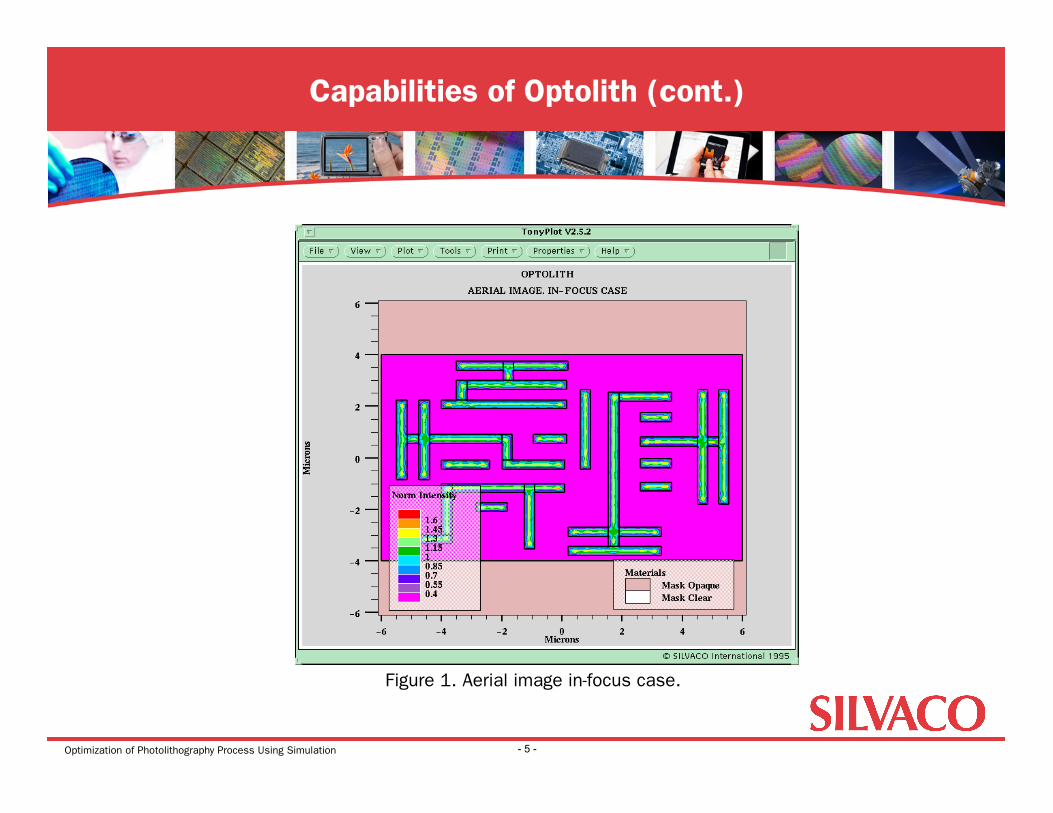
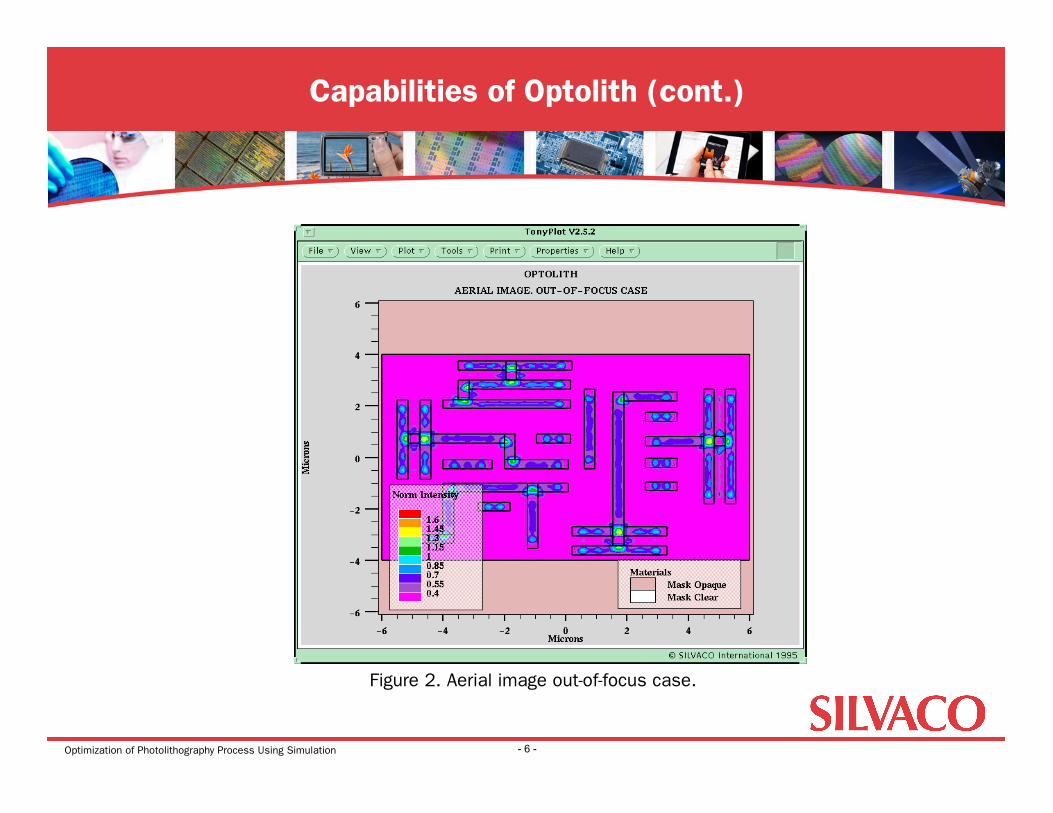
• 2D in and out-of-focus aerial image (Figure 1, Figure 2)
Capabilities of Optolith (cont.)
- 4 -
Optimization of Photolithography Process Using Simulation
Capabilities of Optolith (cont.)
- 5 -
Figure 1. Aerial image in-focus case.
Optimization of Photolithography Process Using Simulation
Capabilities of Optolith (cont.)
- 6 -
Figure 2. Aerial image out-of-focus case.
Optimization of Photolithography Process Using Simulation
• EXPOSE • The latent image formation inside photoresist • The result is the 2D distribution of Photoactive compound (PAC) • Photoresist layer and underlying substrate stack could be non-planar • Beam propagation method simulates all reflection and diffraction effect • Local modification of material optical properties with the absorbed dose • The structure could be result result of Athena simulation (oxidation, deposition, etching
steps) or build using DevEdit
• PRE and POSTEXPOSURE BAKE • Numerical solution of diffusion equation for PAC
Capabilities of Optolith (cont.)
- 7 -
Optimization of Photolithography Process Using Simulation
• DEVELOP • Five models connecting the local photoresist development (etch) rate with the local PAC
concentration • The advance of the photoresist surface is calculated using string algorithm which is
equivalent to local isotropic etching • The string algorithm in Athena is effectively linked with triangle simulation grid
• Allows accurately calculate etch rate in each point of exposed photoresist • Allows final resist area to be triangulated for accurate simulation of subsequent
process steps (etch, implant)
Capabilities of Optolith (cont.)
- 8 -
Optimization of Photolithography Process Using Simulation
• Optical proximity correction based on aerial image metrology • Mask defect inspection • Analysis and control of illumination and optical systems • Advanced mask design (geometry and optical characteristics of Phase
shifters) • Resist characterization using swing curves • Assessment of non-planarity effects for real structures
(Figure 3, Figure 4, and Figure 5)
Applications of Optolith
- 9 -
Optimization of Photolithography Process Using Simulation
Applications of Optolith (con’t)
- 10 -
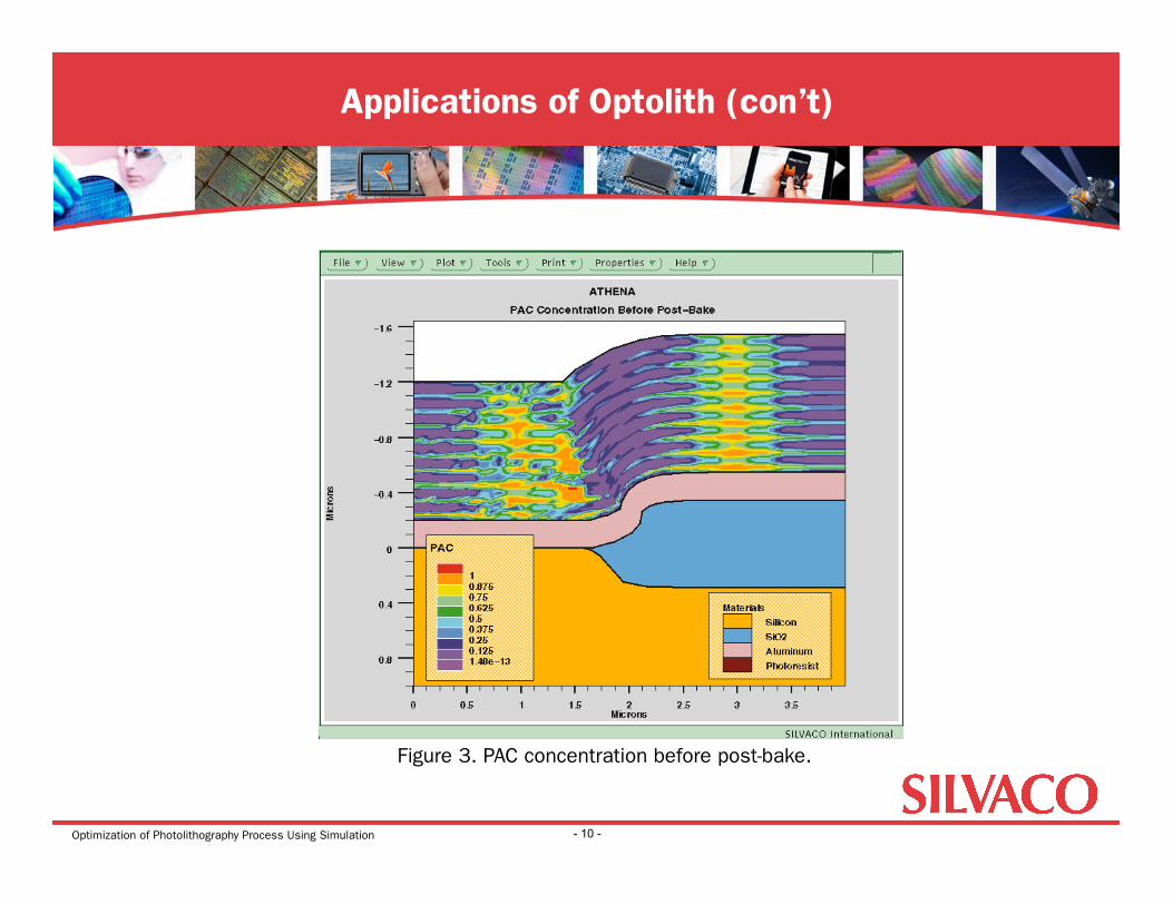
Figure 3. PAC concentration before post-bake.
Optimization of Photolithography Process Using Simulation
Applications of Optolith (con’t)
- 11 -
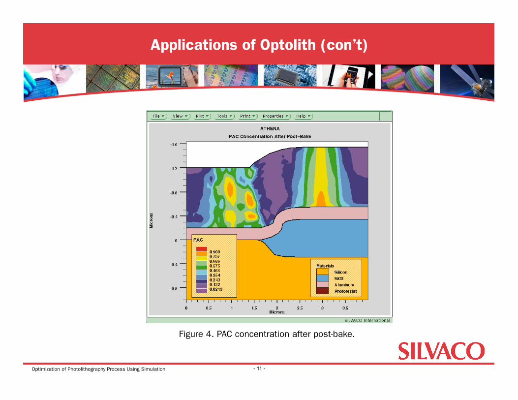
Figure 4. PAC concentration after post-bake.
Optimization of Photolithography Process Using Simulation
Applications of Optolith (con’t)
- 12 -
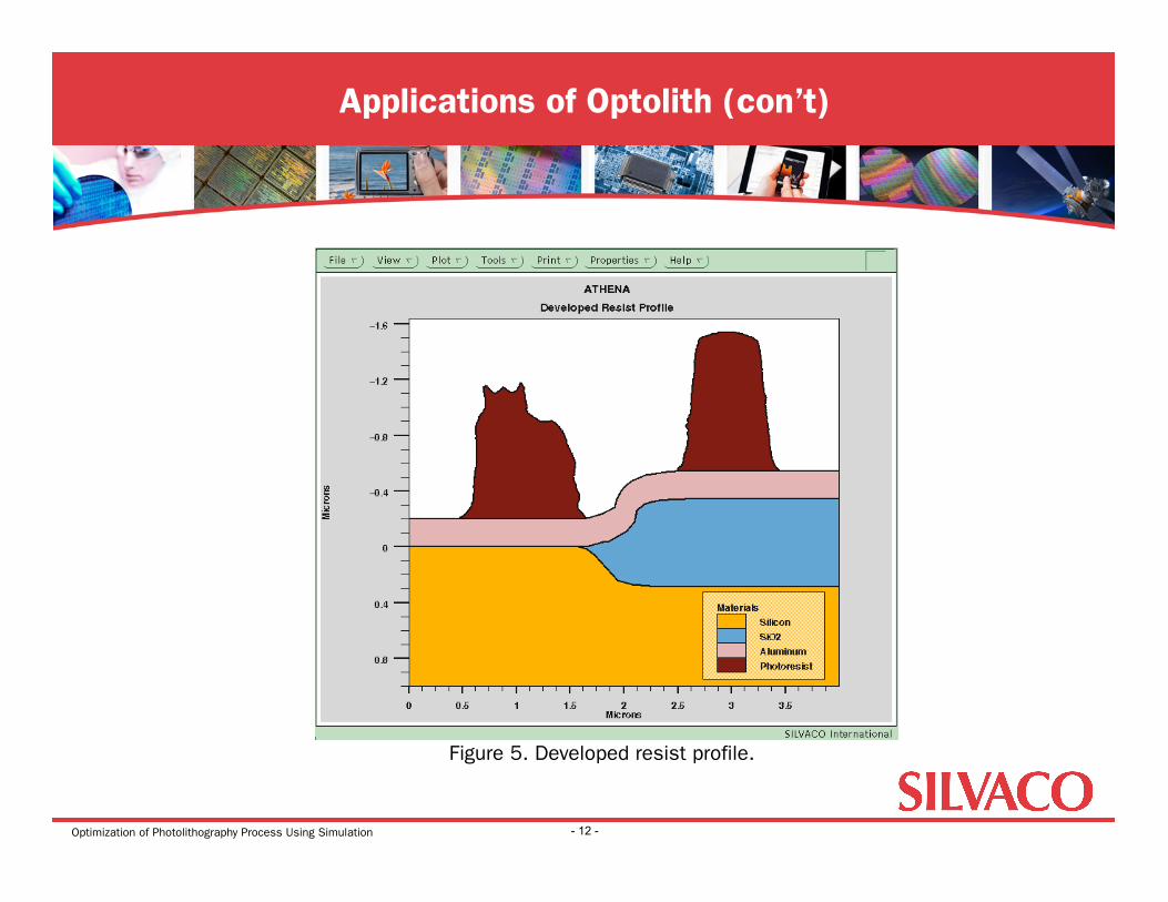
Figure 5. Developed resist profile.
Optimization of Photolithography Process Using Simulation
• One of the most important applications of Optolith is CD control and optimization of stepper parameters to achieve best depth-of-focus and/or exposure latitude
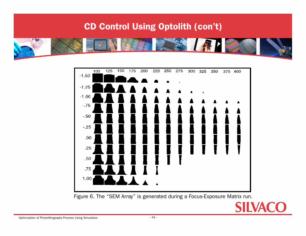
• The complexity of the problem can be seen from the Focus-Exposure Matrix which shows photoresist shapes for 143 combinations of defocus/exposure dose (Figure 6)
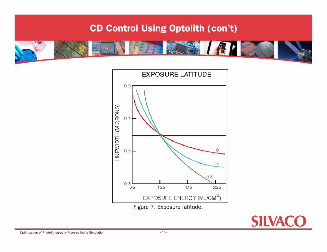
• The first approach to this problem is to use exposure latitude curves (Figure 7)
• However, this approach is obviously insufficient because it even does not give a “window” of defocus and exposure dose values which would result in CDs within certain specifications
CD Control Using Optolith
- 13 -
Optimization of Photolithography Process Using Simulation
CD Control Using Optolith (con’t)
- 14 -
Figure 6. The “SEM Array” is generated during a Focus-Exposure Matrix run.
Optimization of Photolithography Process Using Simulation
CD Control Using Optolith (con’t)
- 15 -
Figure 7. Exposure latitude.
Optimization of Photolithography Process Using Simulation
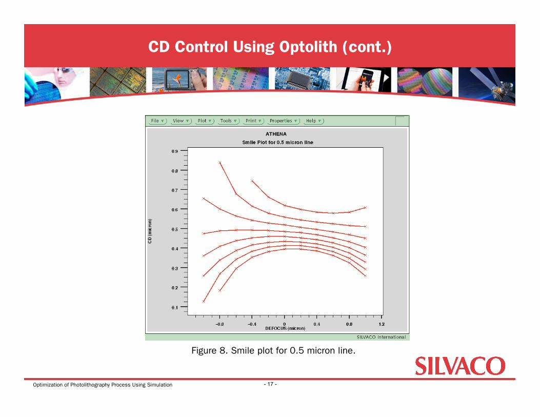
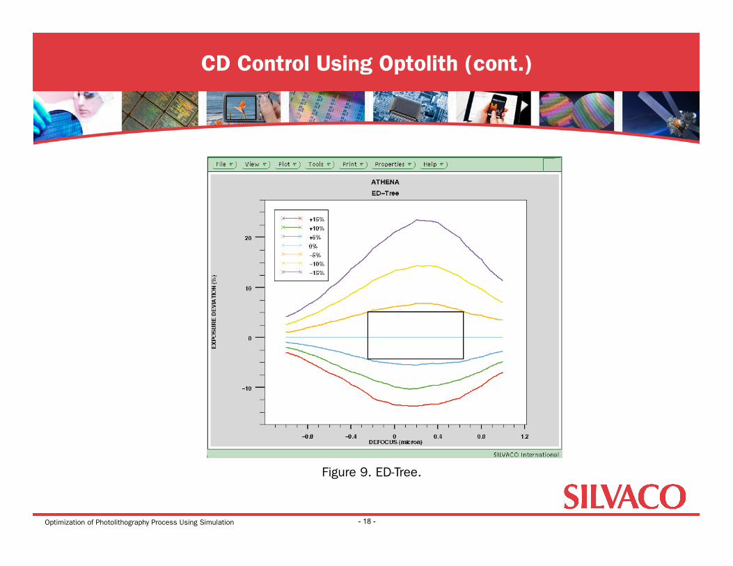
• In order to analyze defocus and exposure effects simultaneously lithography engineers usually use • Smile or Bossung curves (Figure 8) • Exposure Defocus(ED) Tree (Figure 9)
• These two types of analysis are sufficient to estimate optimum defocus and exposure parameters for fixed values of all other process parameters (NA, photoresist thickness, reticle CD, etc.)
• However, these approach could have additional limitations because it uses only one metric parameter (CD measured at the bottom of photoresist)
• Other parameters (resist height, resist sidewall angle) may be needed for accurate process optimization (see Figure 6)
CD Control Using Optolith (cont.)
- 16 -
Optimization of Photolithography Process Using Simulation
CD Control Using Optolith (cont.)
- 17 -
Figure 8. Smile plot for 0.5 micron line.
Optimization of Photolithography Process Using Simulation
CD Control Using Optolith (cont.)
- 18 -
Figure 9. ED-Tree.
Optimization of Photolithography Process Using Simulation
• It is obvious that above methods fail to provide complete CD control and are helpless in process optimization or in simulation model calibration
• The ONLY WAY is: • to use design of experiments (DOE) for several input variables • perform a number of simulations and/or lab experiments • build response surface models (RSM) for selected response factors (e.g. measured CD,
sidewall angle) • use simulated RSMs for multi-parametrical CD control and optimization • automatically fitting of simulated RSMs to experimental ones is only reliable way to
calibrate the empirical parameters involved in simulation
CD Control Using Optolith and VWF
- 19 -
Optimization of Photolithography Process Using Simulation
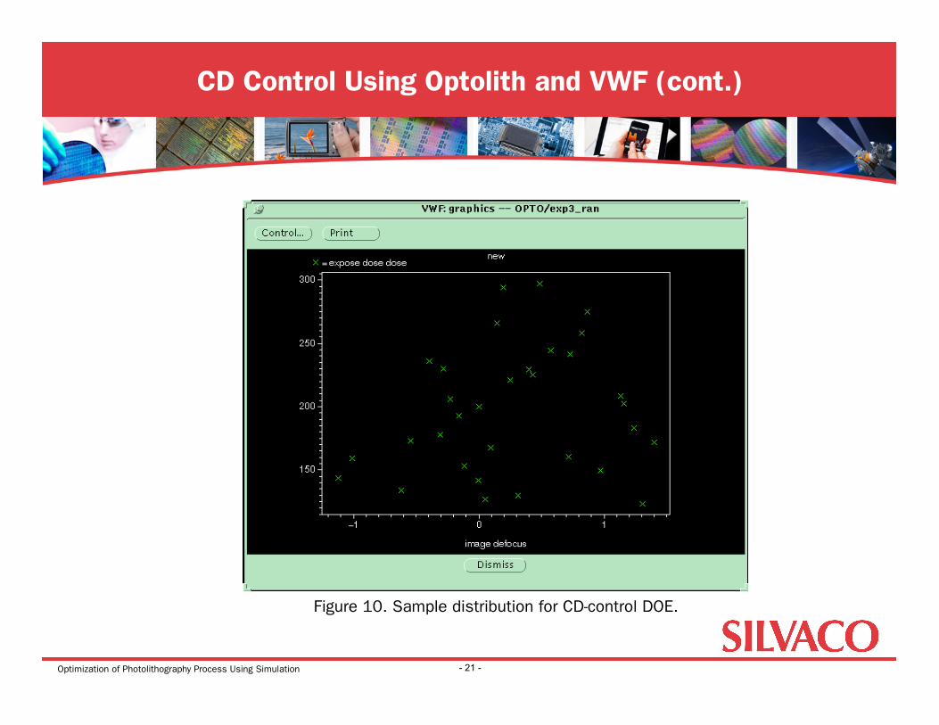
• To prove basic ideas of above approach very simple DOE was prepared • only two input parameters (image defocus and expose dose) are used • Latin Hypercube random design with only 50 branches • Figure 10 shows sample distribution for this experiment (note that the points in upper
corners were eliminated because they result in zero CDs) • Even these few experimental points are enough to build reasonable RSM.
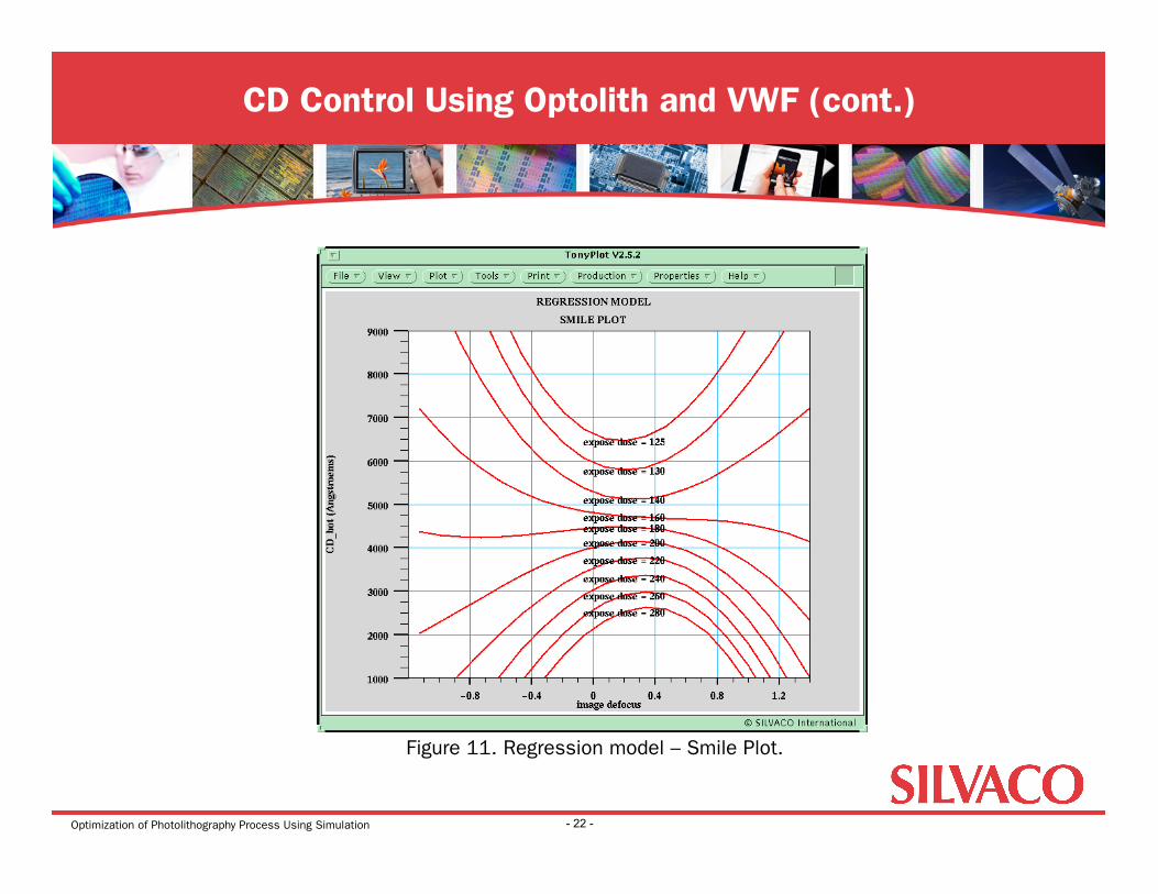
• Resulting RSM allows to build Smile plot for any number expose dose values (Figure 11)
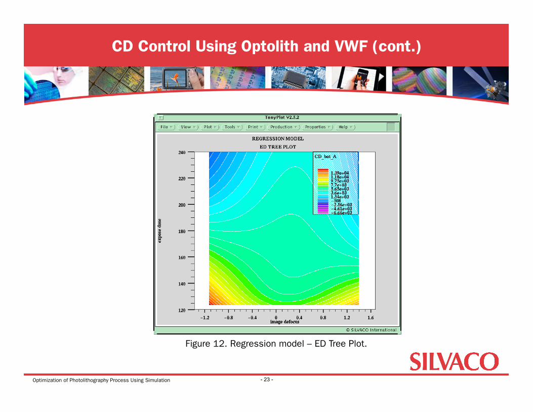
• The same RSM presented as a contour plot (Figure 12) is equivalent to the ED tree plot
CD Control Using Optolith and VWF (cont.)
- 20 -
Optimization of Photolithography Process Using Simulation
CD Control Using Optolith and VWF (cont.)
- 21 -
Figure 10. Sample distribution for CD-control DOE.
Optimization of Photolithography Process Using Simulation
CD Control Using Optolith and VWF (cont.)
- 22 -
Figure 11. Regression model – Smile Plot.
Optimization of Photolithography Process Using Simulation
CD Control Using Optolith and VWF (cont.)
- 23 -
Figure 12. Regression model – ED Tree Plot.
Optimization of Photolithography Process Using Simulation
• Resist thickness was added to the next simulation experiment • This appeared to be not the best selection because it is known that
measured CD varies oscillatory with the resist thickness • Therefore it is very difficult to build RSM which accurately represent all
simulation points • We had to artificially improve quality of RSM by removing some “outlaw”
points • Even after this procedure the RSM can be used for CD control
CD Control Using Optolith and VWF (cont.)
- 24 -
Optimization of Photolithography Process Using Simulation
• Figure 13 - Figure 15 show the change in Smile plot with resist thickness • Figure 16 - Figure 18 show that ED window drastically changes with resist
thickness • CD optimization can be done visually by varying this and/or other parameters and
monitoring which combination would give the biggest “ED window”
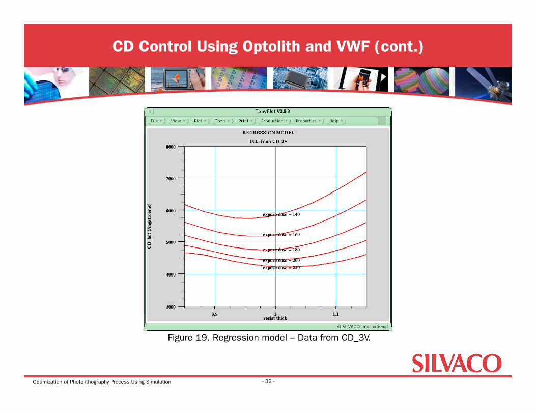
• Figure 19 shows that RSM results in the smooth CD vs thickness curve
CD Control Using Optolith and VWF (cont.)
- 25 -
Optimization of Photolithography Process Using Simulation
CD Control Using Optolith and VWF (cont.)
- 26 -
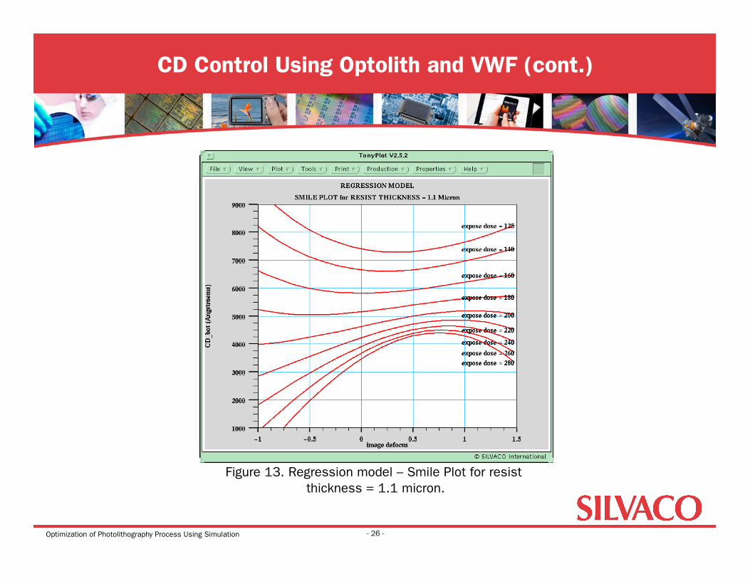
Figure 13. Regression model – Smile Plot for resist thickness = 1.1 micron.
Optimization of Photolithography Process Using Simulation
CD Control Using Optolith and VWF (cont.)
- 27 -
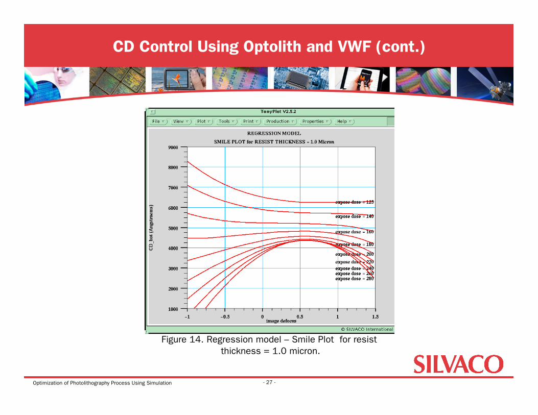
Figure 14. Regression model – Smile Plot for resist thickness = 1.0 micron.
Optimization of Photolithography Process Using Simulation
CD Control Using Optolith and VWF (cont.)
- 28 -
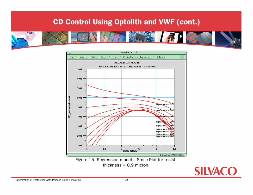
Figure 15. Regression model – Smile Plot for resist thickness = 0.9 micron.
Optimization of Photolithography Process Using Simulation
CD Control Using Optolith and VWF (cont.)
- 29 -
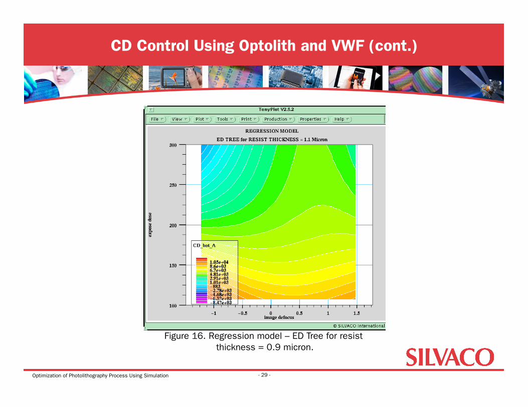
Figure 16. Regression model – ED Tree for resist thickness = 0.9 micron.
Optimization of Photolithography Process Using Simulation
CD Control Using Optolith and VWF (cont.)
- 30 -
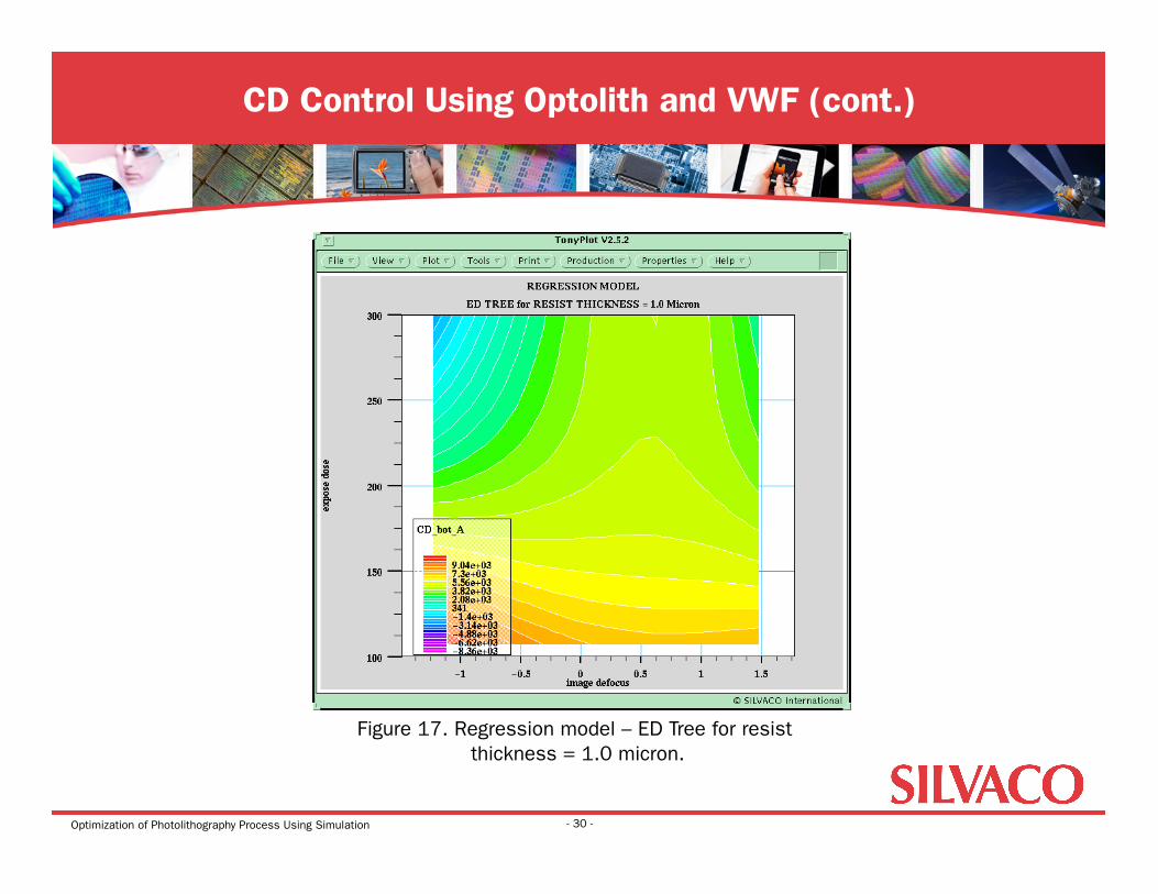
Figure 17. Regression model – ED Tree for resist thickness = 1.0 micron.
Optimization of Photolithography Process Using Simulation
CD Control Using Optolith and VWF (cont.)
- 31 -
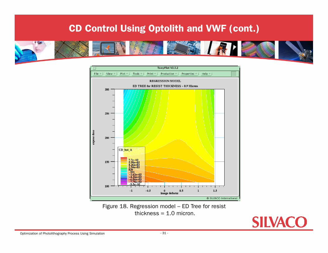
Figure 18. Regression model – ED Tree for resist thickness = 1.0 micron.
Optimization of Photolithography Process Using Simulation
CD Control Using Optolith and VWF (cont.)
- 32 -
Figure 19. Regression model – Data from CD_3V.
Optimization of Photolithography Process Using Simulation
• Because of the wave nature of light, the neighboring mask features will interfere with each other and distort the aerial image integrity. This effect is even more pronounced in the submicron technology • Line shortening • Resist bridging
• There are several options to tackle this problem: • Phase shift mask • Shorter wavelengths • Chemically amplified resist (CAR) • Mask biasing — optical proximity correction (OPC)
Optical Proximity Correction
- 33 -
Optimization of Photolithography Process Using Simulation
• For projection printing, the image of the unbiased mask does not follow the boundaries of the mask features. For instance: • Shortened lines • Wiggling lines • Rounded corners • Image cross-talk
Optical Proximity Correction
- 34 -
Optimization of Photolithography Process Using Simulation
Optical Proximity Correction (con’t)
- 35 -
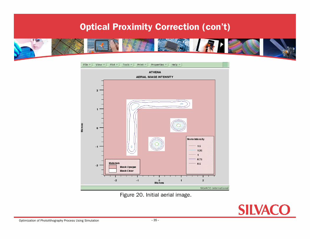
Figure 20. Initial aerial image.
Optimization of Photolithography Process Using Simulation
• Typical mask biasing scheme • Assume the threshold model in the resist response • Increase the length of the mask features • Add / subtract serifs at the corners • Location dependent linewidth
Optical Proximity Correction (con’t)
- 36 -
Optimization of Photolithography Process Using Simulation
Optical Proximity Correction (con’t)
- 37 -
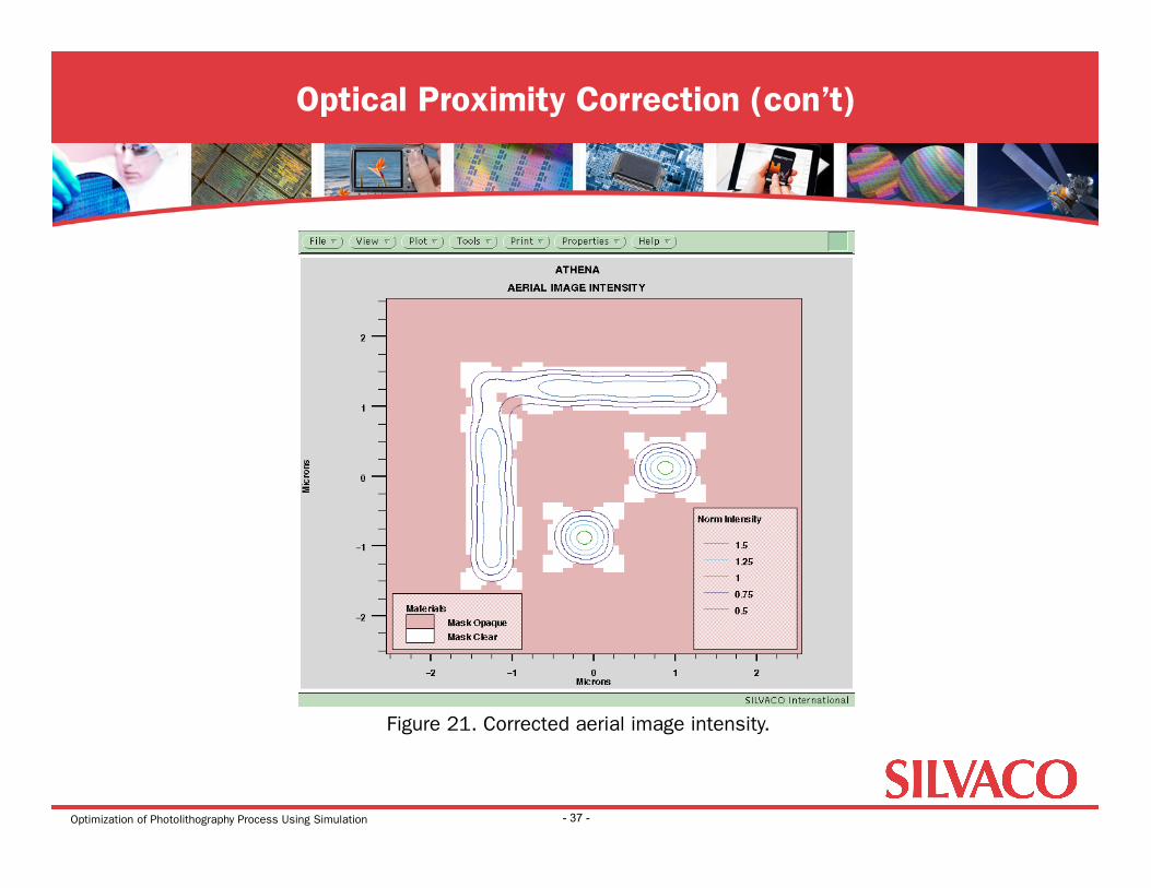
Figure 21. Corrected aerial image intensity.
Optimization of Photolithography Process Using Simulation
• Automated OPC generator • Define a new figure of merit for error estimation • New functionalities in MaskView • Speed up the aerial image calculation (complete) • Special optimization procedures • CD violation checker
Optical Proximity Correction (con’t)
- 38 -
Optimization of Photolithography Process Using Simulation
• Combination of advanced lithography models of Optolith with flexible extraction capabilities of DeckBuild and ability to perform multiple simulation experiments using Virtual Wafer Web Framework allows to optimize and calibrate all lithography processes within realistic non-planar structures
Conclusion
- 39 -