Embed Size (px)
Citation preview
ON-CHIP CHARACTERIZATION OF SINGLE-EVENT
CHARGE-COLLECTION
By
Lakshmi Deepika Tekumala
Thesis
Submitted to the Faculty of the
Graduate School of Vanderbilt University
in partial fulfillment of the requirements
for the degree of
MASTER OF SCIENCE
in
Electrical Engineering
August, 2012
Nashville, Tennessee
Approved:
Professor Bharat L . Bhuva
Professor Lloyd W. Massengill

i
ACKNOWLEDGEMENTS
I would like to thank everyone who has helped me along my way and without whom my work
would not have been complete. Particularly: Dr. Bharat Bhuva for giving me an opportunity to
work under him and for his constant support and motivation during the course of it, Dr. Lloyd
Massengill for serving on my committee and for his insightful discussions and advice, Dr. Tim
Holman for his patient and invaluable advice. Srikanth Jagannathan and Tania Roy for their
inspiration and help. Sincere thanks to all my friends of the Radiation Effects group for their
help.
I am always indebted to my family: my parents, Raja Rao and Uma, my brothers, Sriharsha,
Madhava Rao, my sister-in-law, Padmaja for they have always been extremely supportive of me.
Sincere thanks to my friends Karthick Baskaran, Jugantor Chetia, and Karthik Puvvada for their
encouragement and support.
Lastly, I owe my thanks to the almighty for I would not have been where I am without his grace
and blessings on me.
ii
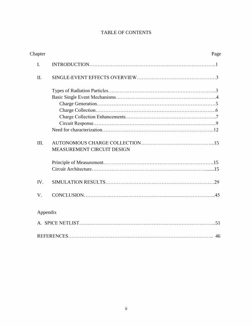
TABLE OF CONTENTS
Chapter Page
I. INTRODUCTION…………………………………………………………………..1
II. SINGLE-EVENT EFFECTS OVERVIEW…………………………………………3
Types of Radiation Particles………………………………………………………...3
Basic Single Event Mechanisms…………………………………………………….4
Charge Generation………………………………………………………………5
Charge Collection……………………………………………………………….6
Charge Collection Enhancements……………………………………………….7
Circuit Response………………………………………………………………...9
Need for characterization…………………………………………………………..12
III. AUTONOMOUS CHARGE COLLECTION……………………………………...15
MEASUREMENT CIRCUIT DESIGN
Principle of Measurement………………………………………………………….15
Circuit Architecture…………………………………………………………….......15
IV. SIMULATION RESULTS…………………………………………………………29
V. CONCLUSION……………………………………………………………………..45
Appendix
A. SPICE NETLIST………………………………………………………………………..51
REFERENCES……………………………………………………………………………. 46
iii
LIST OF FIGURES
Figure Page
1. Illustration of an ion-strike on a reverse-biased p-n junction ……………………..……...6
2. Relevant currents induced in a SOI device after an ion-strike…………………………….8
3. Illustration of parasitic latch-up structure inherent to bulk CMOS technologies……… 11
4. On-chip charge collection measurement circuit developed by Amusan et. al ………….13
5. Delta-encoded DAC architecture………………………………………………………...16
6. Autonomous Charge Collection Measurement Circuit Design………………………….16
7. In response to a positive voltage transient on the target, the counter is enabled………..17
8. Counter increments VDAC until it exceeds Vpeak and the comparator………………….18
disables the counter after VDAC > Vpeak
9. Basic Architecture of a peak detect and hold circuit……………………………………19
10. CMOS peak detect and hold circuit……………………………………………………..20
11. pMOS current mirror as rectifying element……………………………………………..20
12. Basic operation of the PDH circuit……………………………………………………...21
13. Transistor level schematic of CMOS based peak detect and hold circuit……………….22
14. Block diagram of digital-to-analog converter…………………………………………...23
15. 4-bit charge scaling DAC architecture…………………………………………………. 24
16. Equivalent circuit of a 4-bit DAC with MSB ‘high’ and the remaining bits ‘low’……..24
17. Schematic of a comparator circuit………………………………………………………25
18. A differential amplifier with diode connected pMOS loads………………………… 27
19. Rail-rail input swing high-speed differential amplifier……………………………….... 28
20. DAC response to digital input word on every clock cycle…………………………....... 29
iv
21. (a) Transient response of the comparator showing input waveforms………………….. 32
(b) output waveform of the comparator……………………………………………....... 32
22. Peak detected voltage in response to a voltage transient………………………………. 34
23. Charge collected on the hit node for a range of supply voltages 810, 900, …………….37
and 990 mV
24. Charge collection measurements on an ‘off’ pMOS device (‘ff’ process corner)………39
25. Charge collection measurements on an ‘off’ pMOS device (‘ss’ process corner)………39
26. Charge collection measurements on an ‘off’ pMOS device (skewed process corner)…..39
27. Charge collection measurements on an ‘off’ pMOS device using 4-bit and 5-bit………40
DAC
28. Charge based capacitance measurement method……………………………………......44
29. Transistor level schematic of charge based capacitance measurement method………...45
30. Waveform of Vout……………………………………………………………………….45
v
LIST OF TABLES
Table Page
I. Widths and Lengths of transistors used for the 40nm technology design………………...32
II. Widths and lengths of the transistors used for PDH circuit design……………………….34
III. Voltage transient measurements due to an ion-strike on an ‘OFF’ pMOS……………….35
IV. Charge collected on the hit transistor due to an ion strike………………………………..36
V. Voltage transient measurements due to an ion-strike on an ‘OFF’ pMOS…………….....42
VI. Voltage transient measurements due to an ion-strike on an ‘OFF’ pMOS…………….....44
1
CHAPTER I
INTRODUCTION
With a decrease in device dimensions and operating voltages of integrated circuits (ICs), their
sensitivity to radiation increased dramatically [1]. One of the major reliability challenges in deep
sub-micron technologies is single-event effects (SEEs) [2]. When highly energetic particles (
e.g., protons, neutrons, alpha particles or other heavy-ions) strike sensitive regions of
microelectronic circuit, the particle strike may cause a transient disruption of circuit operation
(single-event transient) or a change of logic state of the circuit (single-event upset). These effects
are referred to as soft errors because the device/circuit itself is not permanently damaged by
radiation and the errors can be corrected by new data.
When a radiation particle strikes a semiconductor material, charge is generated either by
direct ionization of the incident particle itself, or due to the ionization by secondary particles
caused due to nuclear reactions between hit device and the incident particle. Following charge
generation, the high electric field present in the reverse biased junction depletion region of the
transistor collects charge through drift and diffusion processes leading to a transient current at
the terminals of the hit transistor.
Using TCAD models, it is possible to examine the charge collection processes after
particle strikes and gain an insight into the mechanisms that occur on a pico-second time scale.
In older technologies, the charge cloud created due to an ion strike affected only a single
transistor due to large separation between them. Thus, the charge collection process in most
2
cases was limited to drift and diffusion processes for a single p-n junction [3]. However for
advanced technology nodes, charge collection process is complex due to several factors, such as
increased carrier concentrations [4], ambipolar carrier mobilities [4], multiple transistors in the
charge track collecting charge [5-6], and parasitic bipolar amplification of single event related
currents [7-12]. Further, the collected charge is also affected by the circuit and layout parameters
at the hit node; such as restoring device characteristics [6] and the presence of multiple devices
within a certain distance [44]. TCAD simulations are limited to just a few devices contained in a
small region due to computational complexities and these effects may or may not be accurately
modeled using TCAD. Hence, experimental verification of charge collection is desirable to
develop accurate predictive TCAD models for future technologies.
This thesis presents an autonomous charge collection measurement circuit technique to
experimentally characterize charge collection, or charge sharing processes, and is organized as
follows. Chapter II provides a brief overview of the various mechanisms of single events and
also some of the existing measurement circuits developed to experimentally characterize single
event charge collection as part of motivation behind this work. Chapter III presents an on-chip
autonomous charge collection measurement technique to experimentally verify charge collection
processes for advanced technologies. Simulation results of the circuit designed in a 40 nm
CMOS process are discussed in Chapter IV. As a conclusion, a summary is provided in Chapter
V.

3
CHAPTER II
SINGLE EVENT EFFECTS – OVERVIEW
Types of radiation particles
This section briefly outlines the space radiation environment in terms of charged particles and its
sources that are capable of affecting integrated circuits (ICs). High energy radiation particles
could be categorized as originating from - (1) Trapped radiation (2) Solar flares and (3) Cosmic
rays
Trapped radiation environment
This includes two major radiation belts that originate from different sources – (1) inner belt that
is formed from the cosmic radiation (also referred to as ‘proton’ belt or ‘Van Allen’ belt) (2)
outer radiation belt trapped in the magnetosphere is composed of plasma or ionized gas
continually emitted by the sun. Van Allen belts are populated by protons of energies between 10-
100 MeV range and hence are referred to as proton belts [13]. As for the outer radiation belt, it is
the sun’s corona that emits the solar wind. When the solar wind activity is high, it diverts the
galactic cosmic rays (another source for single-events) away from the earth’s magnetosphere and
when the activity is weak, it allows these cosmic rays into the earth’s atmosphere.

4
Solar Flares
Solar flares are explosions on the sun’s surface. They are the major source of protons and
electrons. Coronal mass ejections, a type of solar flare occurs when huge bubbles of gas are
ejected from the sun’s surface. They are also found to be rich sources of protons.
Cosmic Rays
Cosmic rays could be classified as – (1) galactic cosmic rays (2) solar cosmic rays and (3)
terrestrial cosmic rays. Galactic cosmic rays are composed of high-energy charged particles from
supernova explosions. These rays are abundant sources of protons although a small percentage (~
1%) of the rays comprise heavy-ions [14]. Solar cosmic rays similar to solar flares originate from
the sun’s surface and are sources of protons, electrons, gamma rays and X-rays. Cosmic rays
penetrate the earth’s atmosphere and interact with the earth’s atmospheric atoms giving rise to
secondary reactions. These consisting mostly of protons, neutrons, electrons, and photons are
primary components terrestrial cosmic rays [15].
Basic Single Event Mechanisms
In the previous section, the sources of radiation particles were identified. This section focuses on
the fundamental mechanisms resulting in single event effects (SEEs). The basic process of
interaction of an ionizing particle with Silicon could be divided into three stages - (1) charge
generation, (2) charge collection, and (3) circuit response [16-18]. Charge generation depends
on the mass and energy of the incident ion and the properties of the materials through which it
passes. Charge collection depends on many factors, such as applied bias, doping concentrations
of the semiconductor, and differs from one transistor to another in the same circuit. Lastly, the
circuit response depends on the circuit topology and determines if the single event (SE) leads to a

5
single-event transient (SET) (a voltage transient that may get latched) or single-event upset
(SEU) (a bit flip in a latch). These processes are discussed below in greater detail.
Charge Generation
When an ionizing particle interacts with the semiconductor material, it releases charge in the
semiconductor material either by - (1) direct ionization by the incident particle itself or (2)
indirect ionization by the secondary particles created by nuclear reactions between the incident
particle and the struck transistor. These processes are briefly discussed as follows -
Direct Ionization
When an ionizing particle passes through the semiconductor material it releases electron-hole
pairs along its path as it loses energy. When the particle loses all of its energy, it comes to rest
having travelled a total length referred to as particle range. To describe the energy loss per unit
path length of the particle, a term called linear energy transfer (LET) is used. Generally to
understand the particle interaction with Silicon, Bragg curves describing LET of particles against
the depths travelled are studied. Such curves are computed using computer codes (TRIM, SRIM
family of codes [19]). For a detailed discussion on Bragg curve, readers are referred to [20].
Typically for heavy-ions, the primary charge deposition mechanism is direct ionization.
Indirect Ionization
Protons and neutrons produce significant upsets due to indirect mechanisms [21-23]. When a
high-energy proton or neutron enters the semiconductor material, any one of these several
interactions may occur – (1) an inelastic collision with the Si target nucleus that may further
result in the emission of alpha or gamma particles and recoil of the daughter nucleus (i.e., Si

6
nucleus may emit an alpha particle and a recoiling Mg nucleus) or (2) spallation reaction in
which the daughter nucleus is broken into fragments each of which can recoil. Any of these
products deposit charge along their paths and induce upsets [24].
Charge Collection
While the previous section discussed the charge generation processes due to irradiation, this
section briefly describes the charge collection processes generated due to an ion-strike. The three
important mechanisms that govern charge collection process are (1) Drift (charge can transport
in response to the built-in or applied electric fields in the device (2) Diffusion (charge can
transport due to carrier concentration gradients in the device) (3) Recombination (carriers of
opposite charge, i.e., electron and hole, may be annihilated due to recombination). As a
consequence of these charge collection and conduction processes, a photocurrent is created at the
terminals of the hit transistor.
When a particle strikes a microelectronic device, the high electric field present in a reverse-
biased junction depletion region collects charge through drift processes and this leads to a current
Figure 1: Illustration of an ion-strike on a reverse-biased p-n junction [25]
7
transient at the terminals of the transistor. Even in the case of strikes near the depletion region of
a transistor, carriers may diffuse into the vicinity of the depletion region field and collect charge
resulting in transient currents. Figure 1 illustrates an ion-strike on a reverse-biased p-n junction.
Additionally, ‘funnel effect’ and its influence on the transient charge collection characteristics
has been investigated by several researchers at IBM [25, 26-27]. While computing the response
of reverse-biased p-n junctions to alpha-particle strikes, researchers found the existence of a
transient disturbance in the junction electrostatic potential and termed this the ‘field funnel’. This
funneling effect may increase the charge collection at the hit transistor by extending the junction
electric field away from the junction and further deep into the substrate. For comprehensive
discussions on funneling, readers are referred to [28-31].
Charge Collection Enhancements
For advanced technologies, charge collection process is complex due to several factors such as
multiple devices along the charge track collecting charge [5-6], increased carrier concentrations
[4], ambipolar carrier mobilities [4], and parasitic bipolar amplification [7-12] of single event
related transient currents. Some of these charge collection enhancement effects are discussed
below briefly.
Parasitic Bipolar Amplification Effect
An effect first observed in Silicon-on-Insulator (SOI) metal oxide semiconductor (MOS) devices,
that could become important for bulk MOS devices, is the parasitic bipolar enhancement effect.
One of the important aspects in modeling SOI devices to an ion-strike is the isolated body
region. Whether this region is electrically floating, or connected to the source region by a low-
resistance strap (body-tie), any charge deposited in this region due to a single event must
8
recombine or exit the region through one of these three methods – (1) across the body-source
junction (2) across the body-drain junction (3) out the body-source tie. Because both the
junctions are reverse biased, most of the ionic charge exits the region via body-source tie. From
the Figure 2, this can lead to the potential gradient from the hit location to the body tie. If the
potential near the hit is large enough to cause minority carrier injection across the body source
junction, then parasitic bipolar action is created between source and the drain. The current
created by the ion-strike is the base current for this parasitic bipolar transistor and this base
current can be amplified to create a large collector current at the sensitive node. Thus, the SE
current is amplified by the gain of the parasitic bipolar transistor [32].
Figure 2: Relevant currents induced in a SOI device after an ion-strike[32]
9
Multiple node charge generation
For deep sub-micron technologies (<250 nm), the effect of a single ion-track can be observed on
multiple circuit nodes through a variety of effects as described in the earlier sections. The most
obvious method that affects the multiple nodes is through diffusion. For multiple transistors in a
common well, the collapse of the well potential by a single ion-strike can affect some or all of
the transistors. Immediately after an ion-strike, carriers are collected by drift process due to the
electric field present in the reverse biased p-n junctions. This is followed by the diffusion of the
carriers from the substrate. For older technologies, the distance between the hit transistor and
secondary transistor was large enough that most of the diffusion charge was also collected by the
hit node. However for advanced technologies, the close proximity of the devices results in
diffusion of charge to nodes other than the hit node. With a very small amount of charge required
to represent a logic HIGH state at the node, the charge collected due to diffusion on an adjacent
node becomes significant. Multi-node charge generation was shown by Olson et al., [33] in an
experiment to determine the cause of single-event upsets at energies lower than expected.
Readers are referred to [33] for further details of interest on multi-node charge collection related
mechanisms.
Circuit Response
The circuit response due to irradiation can either be (1) destructive effect (i.e., hard error) or (2)
temporary effect (i.e., soft error). This section discusses some common destructive and
temporary failure modes

10
Permanent Errors
Permanent errors imply irreversible damage to the functionality of the circuit, typically physical
damage to the device. There are three main types of destructive SEEs – (1) single event burnout
(SEB), (2) single event gate rupture (SEGR), and (3) single event latchup (SEL)
Single-event burnout (SEB) causes permanent damage to power MOSFETS and bipolar
transistors [34-38]. Depending on the currents generated by the ion-strike it turns on the parasitic
or active bipolar device, and triggers a regenerative feedback. If the high current is not limited, a
permanent short occurs between the source and the drain and the device is destroyed [38].
Single-event gate rupture (SEGR) occurs when a charged particle passes through the gate oxide.
This effect was first observed for metal nitride oxide semiconductor (MNOS) used for memory
applications [39]. Later, it was also observed in MOS transistors and power MOSFETs [40].
When an ion passes through the gate oxide, a conducting plasma path is formed between the gate
dielectric and Si substrate. Thus charge flows along the plasma path depositing energy in the gate
oxide. If this energy is high enough, it may cause the local dielectric to melt, and evaporate the
overlying conductive materials. Typically, this failure mechanism not only depends on the oxide
electric field but also on the angle of the ion-strike [41].
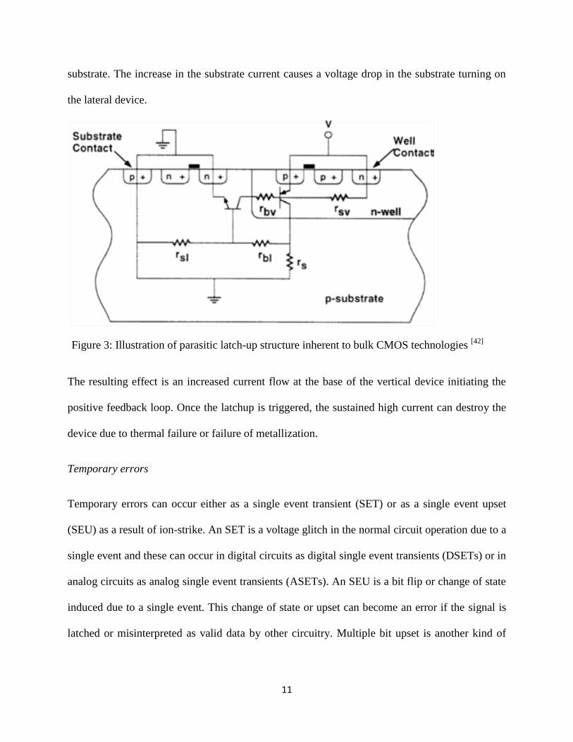
Single-event latchup (SEL) is commonly observed in CMOS process due to the presence of n-p-
n-p junction in the process. The parasitic latchup structure inherent in the CMOS process can be
observed in the Figure 3 [42]. An SEL is initiated when an ion-strike causes a current flow
within the well/substrate junction thereby causing a voltage drop within the well. This voltage
drop leads to the forward biasing of the vertical device leading to an increased current in the
11
substrate. The increase in the substrate current causes a voltage drop in the substrate turning on
the lateral device.
The resulting effect is an increased current flow at the base of the vertical device initiating the
positive feedback loop. Once the latchup is triggered, the sustained high current can destroy the
device due to thermal failure or failure of metallization.
Temporary errors
Temporary errors can occur either as a single event transient (SET) or as a single event upset
(SEU) as a result of ion-strike. An SET is a voltage glitch in the normal circuit operation due to a
single event and these can occur in digital circuits as digital single event transients (DSETs) or in
analog circuits as analog single event transients (ASETs). An SEU is a bit flip or change of state
induced due to a single event. This change of state or upset can become an error if the signal is
latched or misinterpreted as valid data by other circuitry. Multiple bit upset is another kind of
Figure 3: Illustration of parasitic latch-up structure inherent to bulk CMOS technologies [42]

12
temporary error wherein multiple circuits are affected by a single event spreading to multiple
nodes spaced close together.
Need For Characterization
Previous research suggests that charge-collection measurement techniques such as time-resolved
ion beam induced charge collection (TRIBICC) [43] have been effective in measuring charge
collection on individual devices. However, such techniques can be expensive and require large
transistors for viable current measurements. For deep sub-micron technologies, the charge
collected on a hit node is affected by circuit and layout parameters, such as the presence of
multiple devices within a certain distance [6] and the restoring device characteristics [44]. Hence
charge collection measurements must be made on transistors of relevant sizes contained within
the circuit environment. Thus, an on-chip charge collection measurement circuit is desirable as
the time scale of the charge collection process is in the pico-second range. Also, the
measurement circuit must be able to measure be able to measure a wide range of collected
charge within a short time, distinguish effects of parasitic bipolar transistors [10-11], and
measure the effects of charge sharing (i.e., charge collected by multiple devices due to an ion-
strike). Since the charge collection process is of the same order as the switching speeds of the
transistors, the measurement circuit must operate at high speeds.
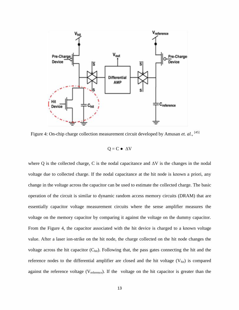
Recently, an on-chip charge collection measurement circuit technique developed by Amusan, et
al., [45] as shown in the Figure 4, has proven effective in measuring charge collection and
charge sharing processes on individual transistors contained within the circuit environment. As
direct measurement of collected charge in the pico-second time scale is difficult, this
measurement circuit is based on an indirect measurement of collected charge given by
13
Q = C ● ΔV
where Q is the collected charge, C is the nodal capacitance and ΔV is the changes in the nodal
voltage due to collected charge. If the nodal capacitance at the hit node is known a priori, any
change in the voltage across the capacitor can be used to estimate the collected charge. The basic
operation of the circuit is similar to dynamic random access memory circuits (DRAM) that are
essentially capacitor voltage measurement circuits where the sense amplifier measures the
voltage on the memory capacitor by comparing it against the voltage on the dummy capacitor.
From the Figure 4, the capacitor associated with the hit device is charged to a known voltage
value. After a laser ion-strike on the hit node, the charge collected on the hit node changes the
voltage across the hit capacitor (Chit). Following that, the pass gates connecting the hit and the
reference nodes to the differential amplifier are closed and the hit voltage (Vhit) is compared
against the reference voltage (Vreference). If the voltage on the hit capacitor is greater than the
Figure 4: On-chip charge collection measurement circuit developed by Amusan et. al., [45]
14
voltage on the reference capacitor then the differential amplifier changes state. However, the
measurement needs to be repeated with multiple values of reference voltage to exactly determine
the voltage on the hit capacitor. The difference in the value of the exact hit voltage (Chit) is then
used to determine the exact collected charge as given by
Q = Creference ● ∆V
Such on-chip measurement techniques have proven effective for measuring charge collection on
individual transistors. However, there are factors, such as the output voltage swing of the
differential amplifier, the capacitor leakage, etc., that limit the accuracy of the measurement
circuit. Also as described previously, multiple measurements may be required with different
values of Vreference to accurately determine the voltage across the hit node. Further, the
measurement circuit must be a self-triggered design since the exact time at which the ion-strike
takes place is usually unknown. Hence, there is a need to overcome these circuit limitations to
make charge collection measurements. The focus of this thesis is on the design of an on-chip
autonomous charge collection measurement circuit technique to overcome these limitations and
hence to accurately quantify single-event charge collection processes for advanced technology
nodes.

15
CHAPTER III
AUTONOMOUS CHARGE COLLECTION MEASUREMENT CIRCUIT
Principle of Measurement
The design of this test circuit is based on the principle that the charge collected at the drain node
of a transistor is directly proportional to the voltage at a circuit node provided only capacitive
loading is present as described in the previous section by -
Q = C ● ΔV
Where Q is the charge collected, C is the nodal capacitance and ΔV is the changes in the nodal
voltage due to collected charge. Any charge collected by a circuit node is also reflected by the
changes in the voltage, assuming the capacitance is unchanged. So, if the nodal capacitance is
known a priori, the change in voltage can be used to determine the charge collected at the circuit
node.
Circuit Architecture
The basic architecture of this measurement circuit is similar to the architecture of a delta encoded
analog-to-digital converter (ADC) or counter-ramp where the input signal and the output from
digital-to-analog (DAC) converter both feed into a comparator as shown in the Figure 5. The
comparator controls a counter and the circuit employs negative feedback from the comparator to
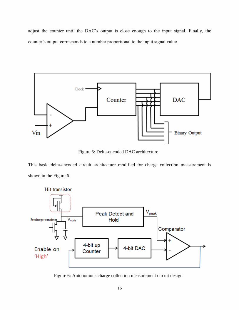
16
adjust the counter until the DAC’s output is close enough to the input signal. Finally, the
counter’s output corresponds to a number proportional to the input signal value.
This basic delta-encoded circuit architecture modified for charge collection measurement is
shown in the Figure 6.
Figure 5: Delta-encoded DAC architecture
Figure 6: Autonomous charge collection measurement circuit design
17
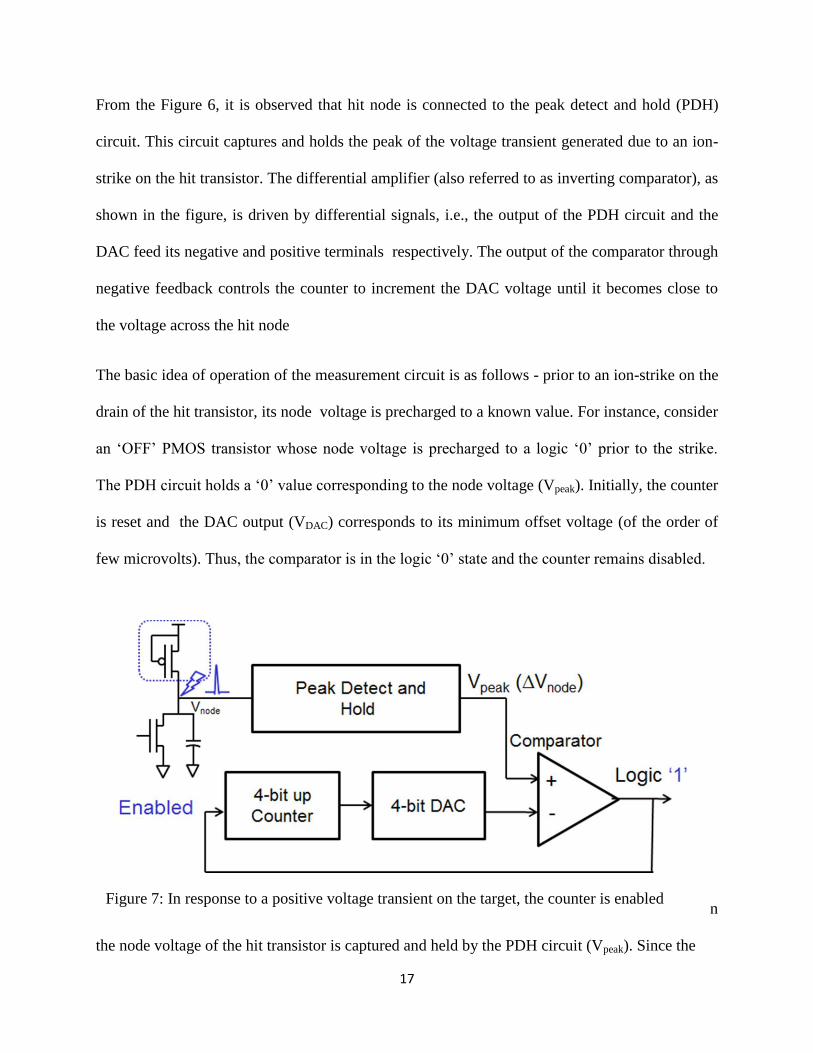
From the Figure 6, it is observed that hit node is connected to the peak detect and hold (PDH)
circuit. This circuit captures and holds the peak of the voltage transient generated due to an ion-
strike on the hit transistor. The differential amplifier (also referred to as inverting comparator), as
shown in the figure, is driven by differential signals, i.e., the output of the PDH circuit and the
DAC feed its negative and positive terminals respectively. The output of the comparator through
negative feedback controls the counter to increment the DAC voltage until it becomes close to
the voltage across the hit node
The basic idea of operation of the measurement circuit is as follows - prior to an ion-strike on the
drain of the hit transistor, its node voltage is precharged to a known value. For instance, consider
an ‘OFF’ PMOS transistor whose node voltage is precharged to a logic ‘0’ prior to the strike.
The PDH circuit holds a ‘0’ value corresponding to the node voltage (Vpeak). Initially, the counter
is reset and the DAC output (VDAC) corresponds to its minimum offset voltage (of the order of
few microvolts). Thus, the comparator is in the logic ‘0’ state and the counter remains disabled.
The initial state of the circuit is shown in the Figure 7. After an ion-strike any change in
the node voltage of the hit transistor is captured and held by the PDH circuit (Vpeak). Since the
Figure 7: In response to a positive voltage transient on the target, the counter is enabled
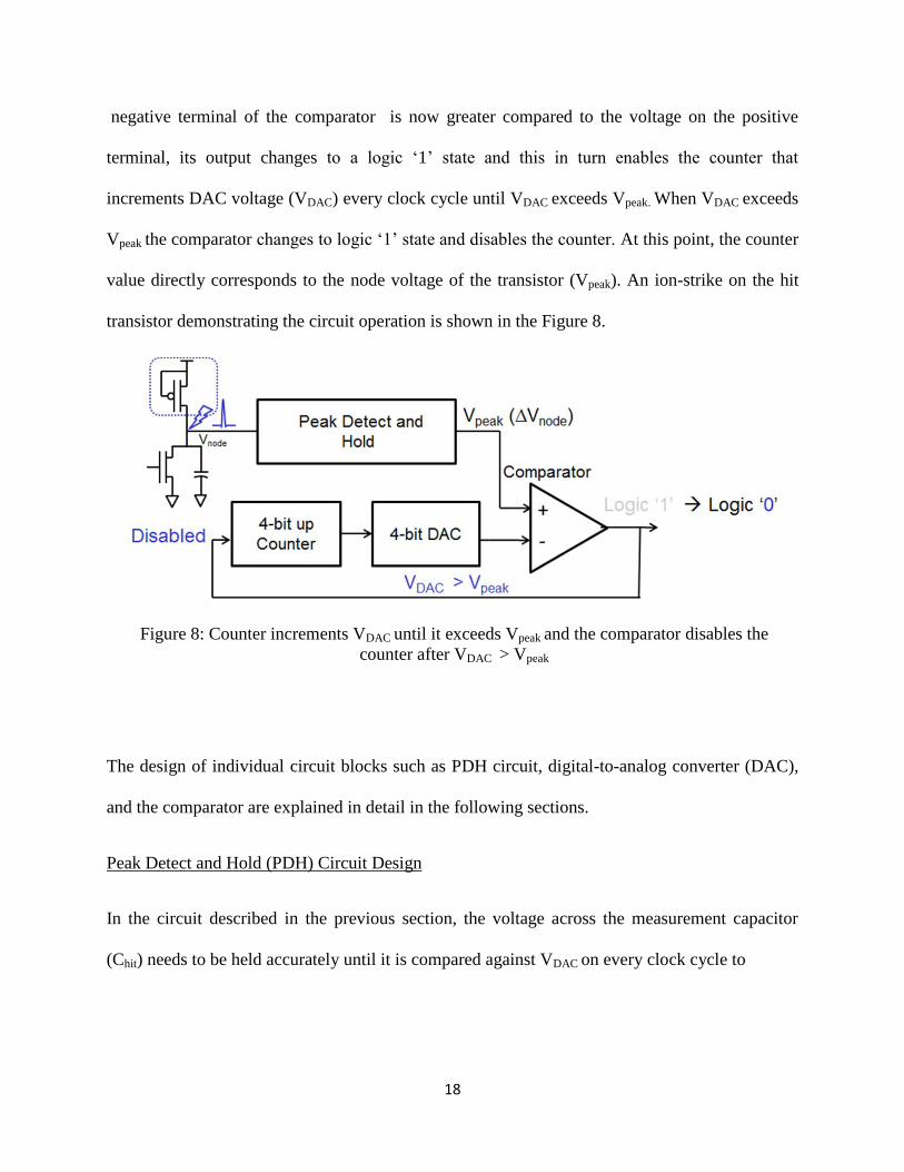
18
negative terminal of the comparator is now greater compared to the voltage on the positive
terminal, its output changes to a logic ‘1’ state and this in turn enables the counter that
increments DAC voltage (VDAC) every clock cycle until VDAC exceeds Vpeak. When VDAC exceeds
Vpeak the comparator changes to logic ‘1’ state and disables the counter. At this point, the counter
value directly corresponds to the node voltage of the transistor (Vpeak). An ion-strike on the hit
transistor demonstrating the circuit operation is shown in the Figure 8.
The design of individual circuit blocks such as PDH circuit, digital-to-analog converter (DAC),
and the comparator are explained in detail in the following sections.
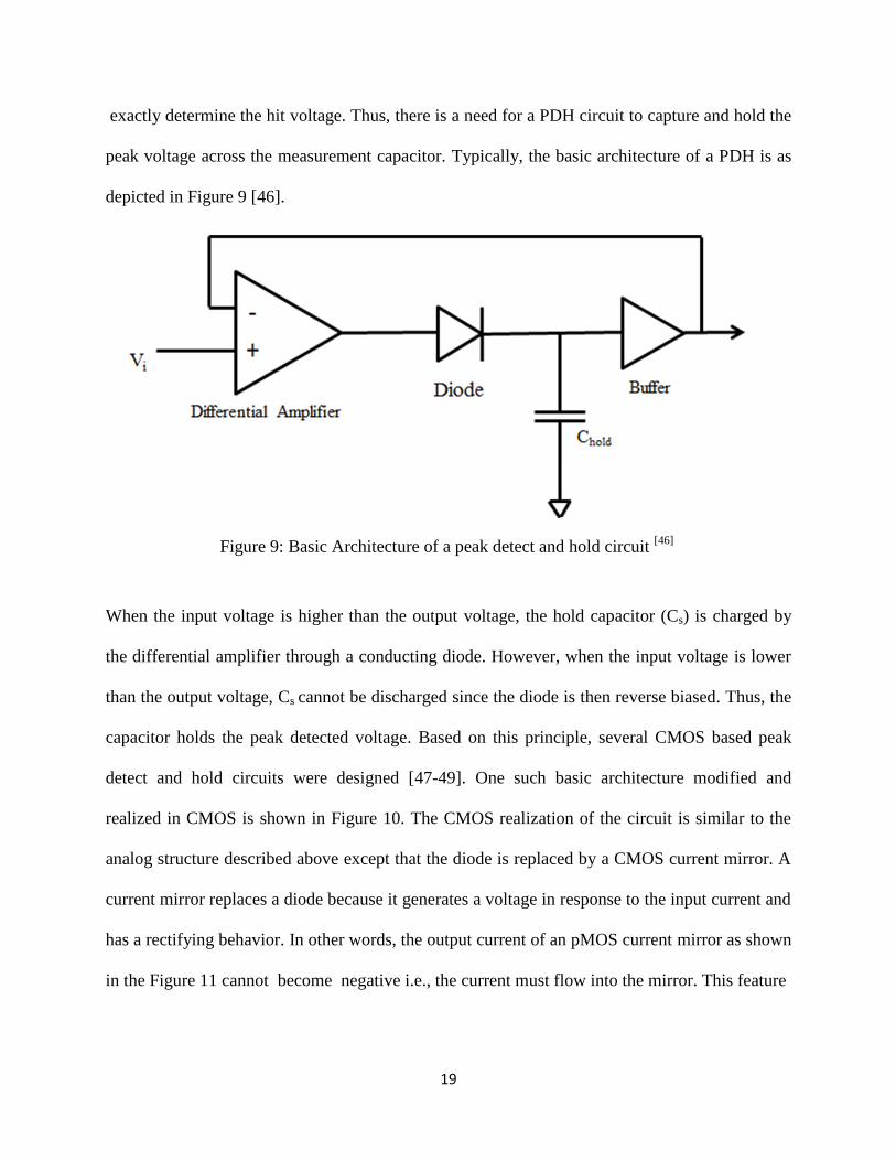
Peak Detect and Hold (PDH) Circuit Design
In the circuit described in the previous section, the voltage across the measurement capacitor
(Chit) needs to be held accurately until it is compared against VDAC on every clock cycle to
Figure 8: Counter increments VDAC until it exceeds Vpeak and the comparator disables the
counter after VDAC > Vpeak
19
exactly determine the hit voltage. Thus, there is a need for a PDH circuit to capture and hold the
peak voltage across the measurement capacitor. Typically, the basic architecture of a PDH is as
depicted in Figure 9 [46].
When the input voltage is higher than the output voltage, the hold capacitor (Cs) is charged by
the differential amplifier through a conducting diode. However, when the input voltage is lower
than the output voltage, Cs cannot be discharged since the diode is then reverse biased. Thus, the
capacitor holds the peak detected voltage. Based on this principle, several CMOS based peak
detect and hold circuits were designed [47-49]. One such basic architecture modified and
realized in CMOS is shown in Figure 10. The CMOS realization of the circuit is similar to the
analog structure described above except that the diode is replaced by a CMOS current mirror. A
current mirror replaces a diode because it generates a voltage in response to the input current and
has a rectifying behavior. In other words, the output current of an pMOS current mirror as shown
in the Figure 11 cannot become negative i.e., the current must flow into the mirror. This feature
Figure 9: Basic Architecture of a peak detect and hold circuit [46]
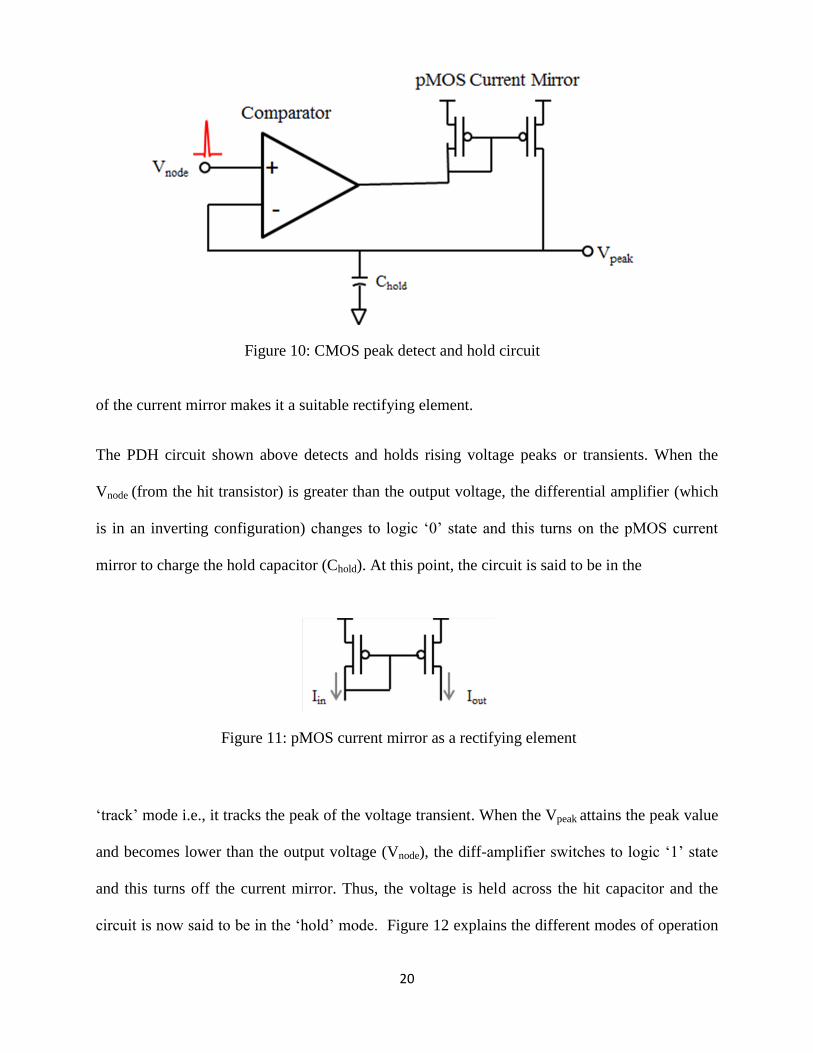
20
of the current mirror makes it a suitable rectifying element.
The PDH circuit shown above detects and holds rising voltage peaks or transients. When the
Vnode (from the hit transistor) is greater than the output voltage, the differential amplifier (which
is in an inverting configuration) changes to logic ‘0’ state and this turns on the pMOS current
mirror to charge the hold capacitor (Chold). At this point, the circuit is said to be in the
‘track’ mode i.e., it tracks the peak of the voltage transient. When the Vpeak attains the peak value
and becomes lower than the output voltage (Vnode), the diff-amplifier switches to logic ‘1’ state
and this turns off the current mirror. Thus, the voltage is held across the hit capacitor and the
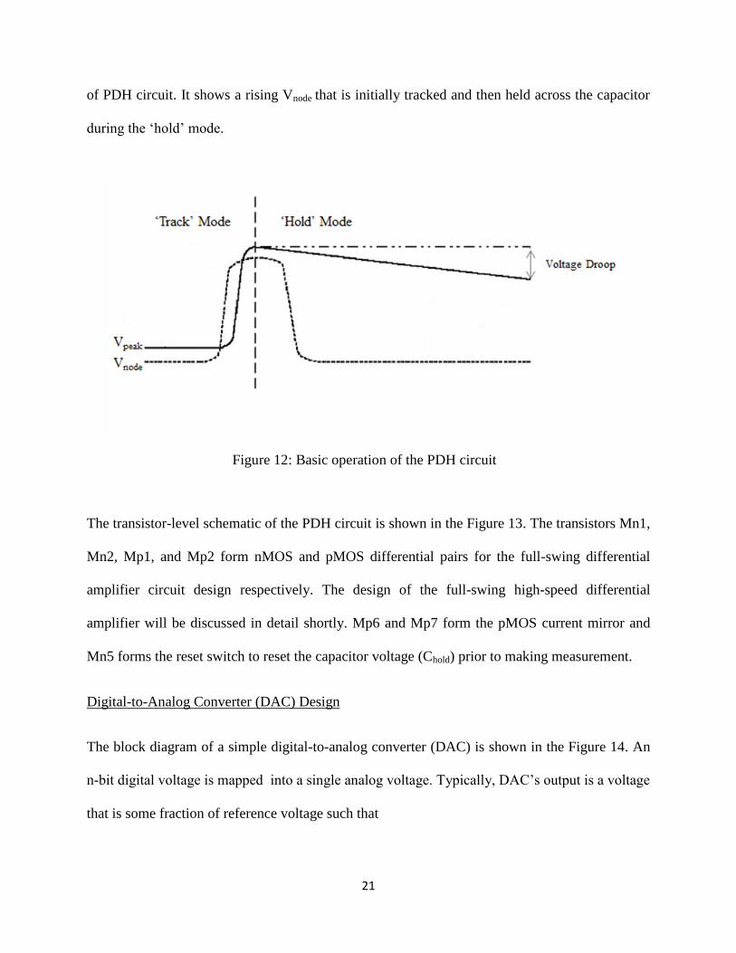
circuit is now said to be in the ‘hold’ mode. Figure 12 explains the different modes of operation
Figure 10: CMOS peak detect and hold circuit
Figure 11: pMOS current mirror as a rectifying element
21
of PDH circuit. It shows a rising Vnode that is initially tracked and then held across the capacitor
during the ‘hold’ mode.
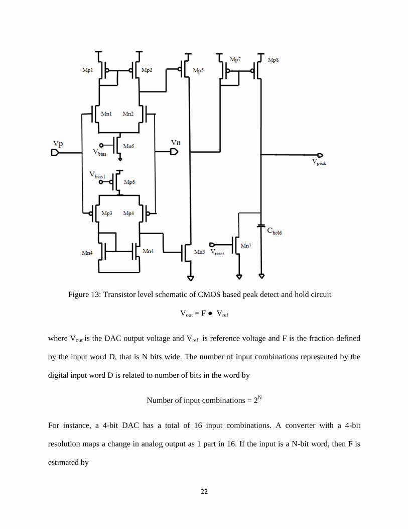
The transistor-level schematic of the PDH circuit is shown in the Figure 13. The transistors Mn1,
Mn2, Mp1, and Mp2 form nMOS and pMOS differential pairs for the full-swing differential
amplifier circuit design respectively. The design of the full-swing high-speed differential
amplifier will be discussed in detail shortly. Mp6 and Mp7 form the pMOS current mirror and
Mn5 forms the reset switch to reset the capacitor voltage (Chold) prior to making measurement.
Digital-to-Analog Converter (DAC) Design
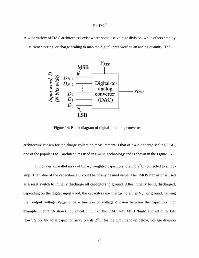
The block diagram of a simple digital-to-analog converter (DAC) is shown in the Figure 14. An
n-bit digital voltage is mapped into a single analog voltage. Typically, DAC’s output is a voltage
that is some fraction of reference voltage such that
Figure 12: Basic operation of the PDH circuit
22
Vout = F ● Vref
where Vout is the DAC output voltage and Vref is reference voltage and F is the fraction defined
by the input word D, that is N bits wide. The number of input combinations represented by the
digital input word D is related to number of bits in the word by
Number of input combinations = 2N
For instance, a 4-bit DAC has a total of 16 input combinations. A converter with a 4-bit
resolution maps a change in analog output as 1 part in 16. If the input is a N-bit word, then F is
estimated by
Figure 13: Transistor level schematic of CMOS based peak detect and hold circuit
23
F = D/2N
A wide variety of DAC architectures exist where some use voltage division, while others employ
current steering or charge scaling to map the digital input word to an analog quantity. The
architecture chosen for the charge collection measurement is that of a 4-bit charge scaling DAC,
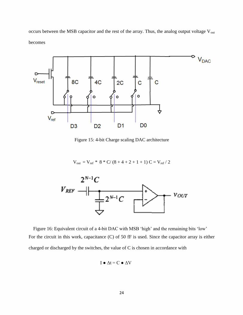
one of the popular DAC architectures used in CMOS technology and is shown in the Figure 15.
It includes a parallel array of binary weighted capacitors totaling 2NC connected to an op-
amp. The value of the capacitance C could be of any desired value. The nMOS transistor is used
as a reset switch to initially discharge all capacitors to ground. After initially being discharged,
depending on the digital input word, the capacitors are charged to either Vref or ground, causing
the output voltage VDAC to be a function of voltage division between the capacitors. For
example, Figure 16 shows equivalent circuit of the DAC with MSB ‘high’ and all other bits
‘low’. Since the total capacitor array equals 2NC, for the circuit shown below, voltage division
Figure 14: Block diagram of digital-to-analog converter
24
occurs between the MSB capacitor and the rest of the array. Thus, the analog output voltage Vout
becomes
Vout = Vref * 8 * C/ (8 + 4 + 2 + 1 + 1) C = Vref / 2
For the circuit in this work, capacitance (C) of 50 fF is used. Since the capacitor array is either
charged or discharged by the switches, the value of C is chosen in accordance with
I ● Δt = C ● ΔV
Figure 15: 4-bit Charge scaling DAC architecture
Figure 16: Equivalent circuit of a 4-bit DAC with MSB ‘high’ and the remaining bits ‘low’
25
where I denotes current flow through the capacitor, ΔV represents change in the voltage across
C, and Δt denotes the time required to charge the capacitance.
The voltage buffer amplifier shown on the schematic (i.e., Figure 15) is used to transfer voltage
from the first circuit with a high output impedance to a second circuit with a low input
impedance. Typically, this is done to prevent the second circuit from loading the DAC circuit
which is undesirable. This unity gain buffer could be implemented either by – (1) applying a full
negative feedback to an op-amp by connecting its output to its inverting input while the DAC
output applied to its non-inverting input. This connection forces the op-amp to adjust its output
voltage equal to the input voltage , or (2) MOS transistor in common drain configuration acts a
unity gain voltage follower. However, for the charge measurement circuit designed as part of this
thesis, the performance of DAC was not affected by its driving circuit ( i.e., inverting comparator
) and if desired, single transistor voltage follower (common drain configuration of MOS) could
be considered as a voltage buffer for the DAC.
Differential Amplifier Design
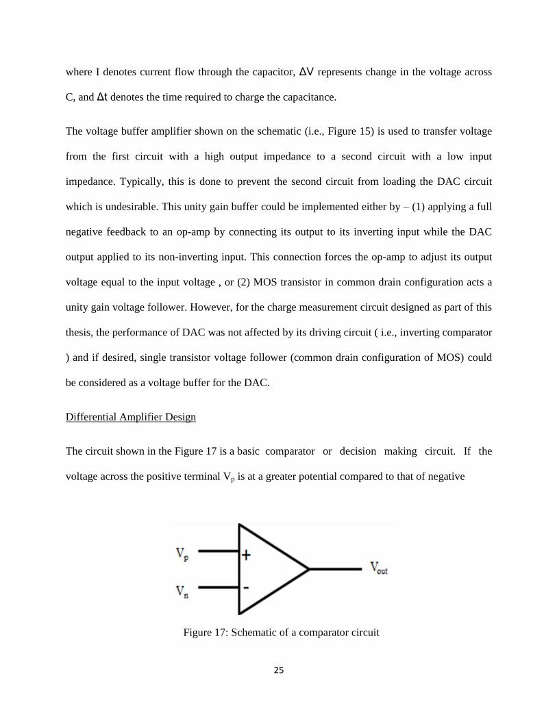
The circuit shown in the Figure 17 is a basic comparator or decision making circuit. If the
voltage across the positive terminal Vp is at a greater potential compared to that of negative
Figure 17: Schematic of a comparator circuit
26
terminal Vn, the output of the comparator is at a logic ‘1’ state and on the other hand, if Vp is at a
lesser potential compared to that of Vn, its output switches to logic ‘0’ state. A simple single-
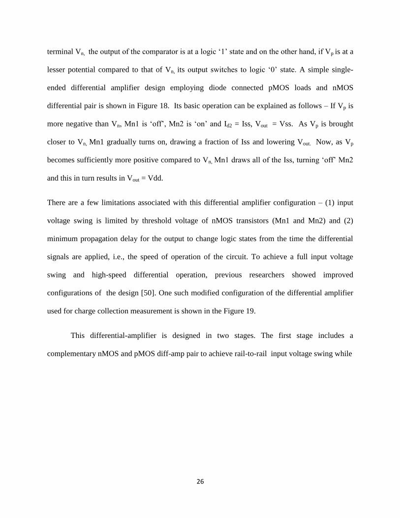
ended differential amplifier design employing diode connected pMOS loads and nMOS
differential pair is shown in Figure 18. Its basic operation can be explained as follows – If Vp is
more negative than Vn, Mn1 is ‘off’, Mn2 is ‘on’ and Id2 = Iss, Vout = Vss. As Vp is brought
closer to Vn, Mn1 gradually turns on, drawing a fraction of Iss and lowering Vout. Now, as Vp
becomes sufficiently more positive compared to Vn, Mn1 draws all of the Iss, turning ‘off’ Mn2
and this in turn results in Vout = Vdd.
There are a few limitations associated with this differential amplifier configuration – (1) input
voltage swing is limited by threshold voltage of nMOS transistors (Mn1 and Mn2) and (2)
minimum propagation delay for the output to change logic states from the time the differential
signals are applied, i.e., the speed of operation of the circuit. To achieve a full input voltage
swing and high-speed differential operation, previous researchers showed improved
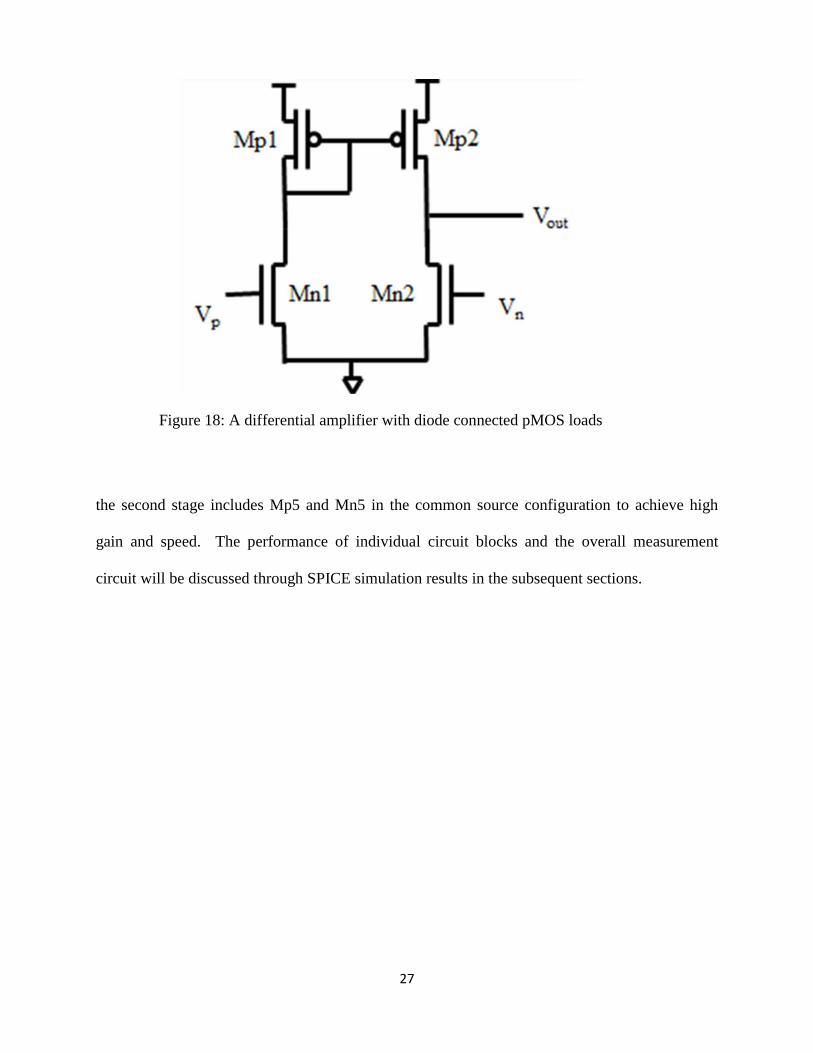
configurations of the design [50]. One such modified configuration of the differential amplifier
used for charge collection measurement is shown in the Figure 19.
This differential-amplifier is designed in two stages. The first stage includes a
complementary nMOS and pMOS diff-amp pair to achieve rail-to-rail input voltage swing while
27
the second stage includes Mp5 and Mn5 in the common source configuration to achieve high
gain and speed. The performance of individual circuit blocks and the overall measurement
circuit will be discussed through SPICE simulation results in the subsequent sections.
Figure 18: A differential amplifier with diode connected pMOS loads
28
29
CHAPTER IV
SIMULATION RESULTS
Simulations were performed in 40 nm UMC Technology using Cadence Spectre simulator [51].
The Spectre is a modern circuit simulator that uses direct methods to simulate analog and digital
circuits at the differential equation level. The basic capabilities of the Spice circuit simulator are
similar in function and application to SPICE.
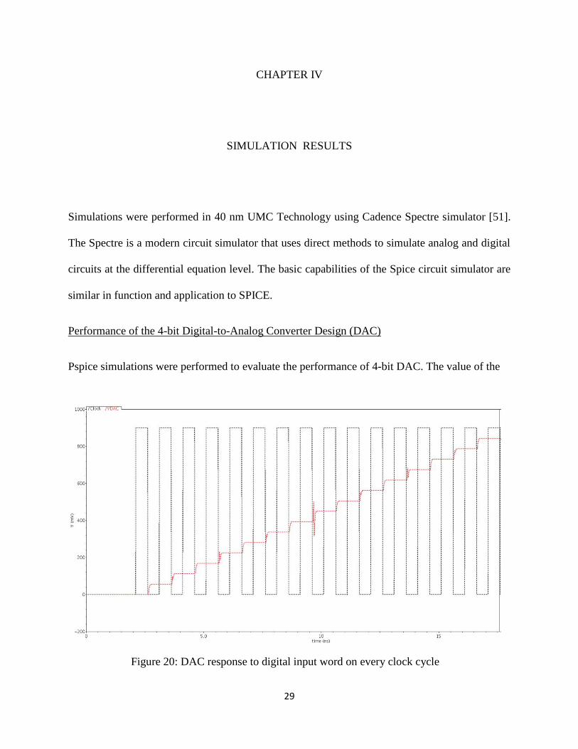
Performance of the 4-bit Digital-to-Analog Converter Design (DAC)
Pspice simulations were performed to evaluate the performance of 4-bit DAC. The value of the
Figure 20: DAC response to digital input word on every clock cycle
30
binary weighted capacitance (C) used for simulations is 50 fF. The DAC output in response to
the 4-bit digital inputs is shown in the Figure 20. The digital input word is applied to the DAC
through a counter and its clock waveform is as shown in the figure above. On every clock cycle,
the DAC’s output voltage is represented by the waveform in blue color.
For a reference voltage of 0.9V, the plot shows that the DAC output voltage increments in steps
of 56.25 mV and this is described as ‘resolution’ of the data converter. Typical specifications of
this design are described below –
Offset error
Typically, the DAC output voltage for input word D = 0 should be 0. However, due to non-
idealities, there is offset voltage associated with the design even when D = 0. For the design used
in our work, the offset voltage is estimated to be 0.25 LSB.
Differential non-linearity error (DNL error)
Ideally, each adjacent output increment should be exactly one sixteenth (for a 4-bit DAC) of the
reference voltage. Thus, each ideal increment corresponds to 1 LSB, i.e., 56.25 mV. However,
non-ideal components cause the analog increments to differ from their ideal values. This
difference between ideal height of increment and the actual incremental height is defined as
differential non-linearity
Differential Non-Linearity (DNLn) = Ideal height of transition – actual height
Where ‘n’ corresponds to the digital input. This specification is measure of how accurately the
DAC can generate uniform analog LSB multiples at its output. The DNL for the entire converter
is calculated to be - 0.0019 LSB

31
Gain Error
For a non-ideal DAC, a gain error exists if the slope of the transfer curve obtained from
simulating DAC is different from the slope of the best-fit line for the ideal DAC. This design has
a gain error of 0.04 LSB
The circuit simulations are carried out using a 4-bit DAC and the design-tradeoffs associated
with further implementing the charge collection measurement circuit design using higher-order
DAC circuit designs are discussed in the design trade-offs section.
Performance of differential amplifier (inverting comparator)
The inverting comparator design as discussed in the previous section is simulated to characterize
its performance. The transistor sizes are as listed in the Table I. The transistors Mn1, Mn2
(nMOS diff-pair) and Mp1, Mp2 (pMOS diff-pair) are sized to set the diff-amp
transconductance (gm, sets the gain of the stage) as well as the input capacitance. The pMOS and
nMOS current mirror loads are sized to match the bias currents set by the diff-pairs. The
transistors Mp5, and Mn5 are sized to achieve high gain and increased speed of operation. The
design procedure could be iterated with these equations -
Differential voltage gain of the diff-amp (Av) = gm1 (ron2 || ron4 ) or gm1/(gds2 + gds4 )
Maximum common mode voltage (VIC(max)) = Vdd – Vsg3 + Vtn1
Minimum common mode voltage (VIC(min)) = Vss + Vds5(sat) + Vgsn1
It is desirable for the circuit to have a wide common-mode range which is the range of voltage
over which the differential-amplifier continues to sense and amplify the differential inputs with
the same gain. The detailed calculations to determine the transistor sizes are shown below by
32
considering the case of nMOS diff-amp pair with pMOS current mirror loads. The same applies
to its complementary diff-pair i.e., the pMOS diff pair with nMOS current mirror load.
(1) VIC(max) = Vdd – Vsg3 + Vtn1, for a VIC(max) = 800 mV
800 mV = 900 mV – Vsg3 + 280 mV
Vsg3 = 380 mV = √ (2. Iss / (Kn. (W3/L3))) + Vtn3, for Iss of 50 uA hand calculations
suggest (W3/L3) = (W4/L4) = ~30
(2) Keeping the tail-current fixed, it is desirable to calculate the transistor sizes of Mn1 and
Mn2 and they are determined from the gain equation given by -
Av = gm1 / (gds2 + gds4) = (√ (2. Kn1. (W1/L1)) / (lambdap + lambdan) √Iss), where
lambda is the channel length modulation parameter, Iss = 50 uA.
Initially, gain of ~70 is assumed and this may be altered depending upon the (W1/L1) obtained.
Substituting the values in the gain equation above gives (W1/L1) = ~15. The upper limit on the
chosen gain is to pick W1/L1 such that the input capacitances are lower.
(3) Now, the tail-bias current transistor sizes are determined from the minimum common
mode voltage equation given by –
VIC(min) = Vss + Vds5(sat) + Vgsn1, for a VIC(min) = ~1/2. Vdd (i.e., 500 mV)
Vds5(sat) = 500 mV – √(2. Iss / Kn. (W1/L1)) – Vtn1, for Iss = 50 uA, W1/L1 = 15
calculations suggest a Vds(sat) of ~200 mV. From this, (W5/L5) is obtained by –
W5/ L5 = (2. Iss)/ (Kn. Vds(sat)2) = ~35
From the Vds(sat), Vbias for the tail current source i.e., Vgs5 is fixed ~400 mV
33
From the design, the common mode range is extended on the lower limit through the pMOS diff-
amp and its calculations are similar to the equations described above for the nMOS diff-pair
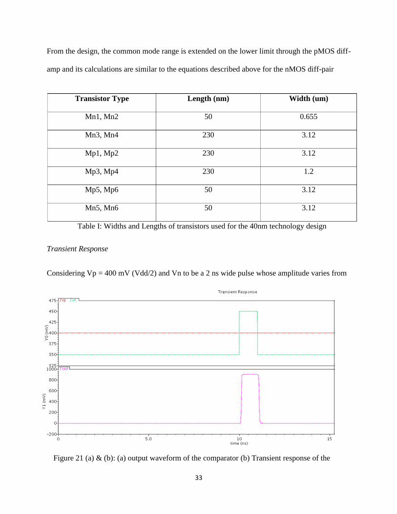
Transient Response
Considering Vp = 400 mV (Vdd/2) and Vn to be a 2 ns wide pulse whose amplitude varies from
Figure 21 (a) & (b): (a) output waveform of the comparator (b) Transient response of the
comparator showing input waveforms
Transistor Type Length (nm) Width (um)
Mn1, Mn2 50 0.655
Mn3, Mn4 230 3.12
Mp1, Mp2 230 3.12
Mp3, Mp4 230 1.2
Mp5, Mp6 50 3.12
Mn5, Mn6 50 3.12
Table I: Widths and Lengths of transistors used for the 40nm technology design

34
350 mV to 450 mV, i.e., the positive terminal is 50 mV above the negative input. The transient
response of the comparator with these inputs is as shown in the Figure 21 (a) & (b).
Propagation Delay
Ideally, propagation delay defined as the time difference between the input Vp crossing the
reference voltage Vn and the output changing logic states is zero. However, the maximum
propagation delay for this design is calculated to be 300 ps.
Peak Detect and Hold Circuit Performance
The transistor sizes used in the design of the circuit are as listed in the Table II. The comparator
used for PDH circuit design is exactly similar to the comparator design discussed in the earlier
section and the design equations to determine the transistor sizes for the differential amplifier are
also as discussed in the earlier section. The pMOS transistors (Mp7, Mp8) of the current mirror
are minimally sized (for a given technology) transistors. Minimal sized transistors are desirable
to reduce the leakage due to the current mirror during the ‘hold’ mode (which results in ‘positive
voltage droop’). For the chosen width (W) and length (L) of pMOS current mirrors, the leakage
current is estimated to be ~5 nA. This is estimated from the leakage current equations -
Ioff (nA) = Io (W/L) eq(vgs – vt)/KT
Similarly, the nMOS reset switch (Mn7) is sized to compensate for the leakage current estimated
above. This is done to minimize the ‘voltage droop’ due to the nMOS transistor. In the circuit
designed, although the positive and the negative voltage droops are reduced by sizing W/L, the
pMOS current mirror still results in a worst-case ‘droop’ of 150 uV/ usec. The value of the hold
35
capacitor is determined by the range of expected charge collected which in this case is chosen to
be 100 fF (to account up to ~90 fC of collected charge)
Simulations results shown in the Figure 22 include the peak detected voltage for a peak voltage
of 600 mV. Results indicate that voltage droop is about 150 uV/ usec and the maximum peak
detection voltage offset/error is ± 25 mV (this is not observed in the plot).
Figure 22: Peak detected voltage in response to a voltage transient on a single ‘OFF’
pMOS transistor
Transistor Type Length (nm) Width (um)
Mn1, Mn2 50 0.655
Mn3, Mn4 50 3.12
Mp1, Mp2 230 3.12
Mp3, Mp4 230 1.5
Mp5,Mp6 50 3.12
Mn5, Mn6 50 3.12
Mp7, Mp8 50 1.5
Mn7 50 0.4
Table II: Widths and lengths of the transistors used for PDH circuit design
36
The plot shows a Vreset pulse applied for a period of 1 ns to discharge the hold capacitor prior to
an ion-strike on the ‘OFF’ pMOS transistor. Vhit shown in the plot (the curve shown in ‘green’
color) shows a change in the node voltage of the ‘hit’ transistor due to an ion-strike (the
transient is modeled as a bias-dependent single-event model). After an ion-strike, a change in
the node voltage is detected and held by the PDH circuit which is as shown in the Figure 22.
Charge Collection Measurement Circuit
The test structure (a nominal Vt ‘OFF’ pMOS device) with a 100 fF capacitor was simulated for
charge collection measurements. A bias-dependent single-event model [45] was used to simulate
the transient generated due to an ion-strike. This model was recently developed to capture the
dynamic charge collection interactions represented in TCAD. The development of this model
was based on the fact that charge collection dynamically interacts with the circuit response. The
interested reader is directed to [52] for further details on the model.
Table III shows the results of charge collection measurements as a result of ion-strikes on the test
structure. These simulations were carried out at a nominal supply voltage of 900 mV and the
counter operating at 1 GHz. From the table, Vnode represents the change in the voltage due to the
Vnode (mV) Vpeak (mV) Counter Value (C) Vmeasured[C * DACresolution] (mV)
358.7 368.9 0111 393.75
440.6 441 1000 450
526.3 519 1001 506.2
612 595 1011 618.75
672.2 660.5 1100 675
789.4 759.8 1101 787.5
Table III: Voltage transient measurements due to an ion-strike on an ‘OFF’ pMOS
37
strike on the circuit node and Vpeak is the peak value of the voltage captured by the PDH circuit.
Vmeasured calculated from the counter output represents the hit voltage measured by the circuit.
Based on the counter value seen at the circuit output, Vmeasured is calculated from the DAC
resolution as –
Vmeasured = Counter output x DACresolution
Now, the charge collected is calculated as the nodal capacitance times the voltage measured
across the hit node - Qmeasured = C * Vmeasured
Table IV shows the calculated values of charge collected for a capacitance size of 100 fF and a
supply voltage of 900 mV. The circuit resolution is calculated to be 5 fC which is determined by
the DAC resolution (56.25 mV for the 4-bit DAC used in this circuit). However, there is a
voltage offset/ error associated with the circuit which is defined as the difference between the
actual hit node voltage (Vnode) and the measured output voltage of the DAC (VDAC) and this
worst-case voltage error is estimated to be ± 1 LSB (where 1 LSB = 56.25 mV (or) 5 fC).
Qnode (fC) Counter Value (C) Qmeasured [C * DACresolution] (fC)
35.87 0111 39.37
44.06 1000 45
52.63 1001 50.62
61.2 1011 61.87
67.22 1100 67.5
78.94 1101 78.75
Table IV: Charge collected on the hit transistor due to an ion-strike
38
Impact of Supply Voltage Variation
Variations in the supply voltage can cause variations in the circuit performance. Simulations
were carried out to characterize the circuit performance for a ± 10 % variation in the supply
voltage. Figure 23 shows a plot of charge collected on the hit transistor for a range of supply
voltage values of 810, 900, and 990 mV respectively. While the black line represents ideal linear
relationship between the actual and measured values, the red curves represent the measurements
at different supply voltages. It is observed that for a ± 10% voltage variation, the minimum
offset/ voltage error is estimated to be within ± 1 LSB ( 1 LSB = 56.25 mV (or) 5 fC). To reduce
the circuit sensitivity to supply variations and improve its accuracy of measurement, on-chip
decoupling capacitors are connected between supply and the ground. The added capacitor not
only filters out any ac fluctuations that appear on the supply rail but also supplies the needed
charge during the transient times. Hence, it keeps the voltage applied across the circuit at Vdd.
Hand calculations suggest that the amount of decoupling capacitance required to suppress a ±
Figure 23: Charge collected on the hit node for a range of supply voltages 810, 900, and 990
mV

39
10% variation on Vdd lines is ~ 20 pF. As such high values are not practical on-chip, off-chip
capacitors are used across the power and ground pins.
Impact of process variations
Variations in the manufacturing process parameters result in large shifts in individual transistor
parameters and affect the circuit response . These variations include gate depletion [53], surface
state charge [54], line edge roughness [55], random dopant fluctuations [56-57] and so on.
Process variations can cause large variations in chip-level parameters such as standby leakage
current (due to variations in the channel length and threshold voltage) and operating frequency.
Hence, process- and transistor- parameter variations pose a serious challenge for circuit design at
advanced technology nodes.
For semiconductor fabrication, process corners represent a six sigma variation from nominal
doping concentrations and other parameters in transistors on a silicon wafer. This variation can
cause significant changes in the circuit performance. To characterize the circuit performance for
process variations, simulations were performed at four different process corners – (1) fast nMOS
and fast pMOS (referred to as ‘ff’ process corner) (2) slow nMOS and slow pMOS (also referred
to as ‘ss’ process corner) (3) fast nMOS and slow pMOS (the ‘fnsp’ process corner) and finally
(4) slow nMOS and fast pMOS (‘snfp’ process corner). The first two corners are referred to as
even corners because both n- and p-FETS are equally affected and this generally does not
adversely affect the logical correctness of the circuit. On the other hand, the last two corners are
referred to as skewed corners because one type of device switches faster than the other. Figures
24-25 show the measurements obtained at even process corners.
40
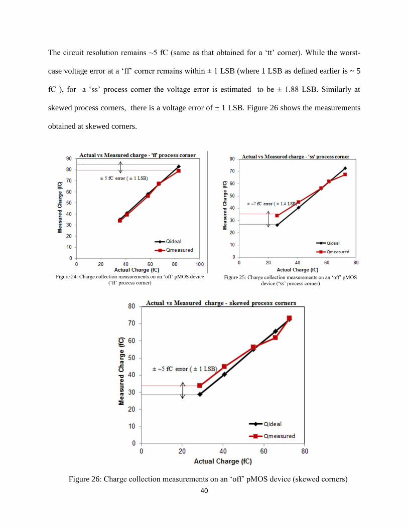
The circuit resolution remains ~5 fC (same as that obtained for a ‘tt’ corner). While the worst-
case voltage error at a ‘ff’ corner remains within ± 1 LSB (where 1 LSB as defined earlier is ~ 5
fC ), for a ‘ss’ process corner the voltage error is estimated to be ± 1.88 LSB. Similarly at
skewed process corners, there is a voltage error of ± 1 LSB. Figure 26 shows the measurements
obtained at skewed corners.
Figure 24: Charge collection measurements on an ‘off’ pMOS device (‘ff’ process corner)
Figure 25: Charge collection measurements on an ‘off’ pMOS device (‘ss’ process corner)
Figure 26: Charge collection measurements on an ‘off’ pMOS device (skewed corners)
41
Design Trade-offs and Considerations
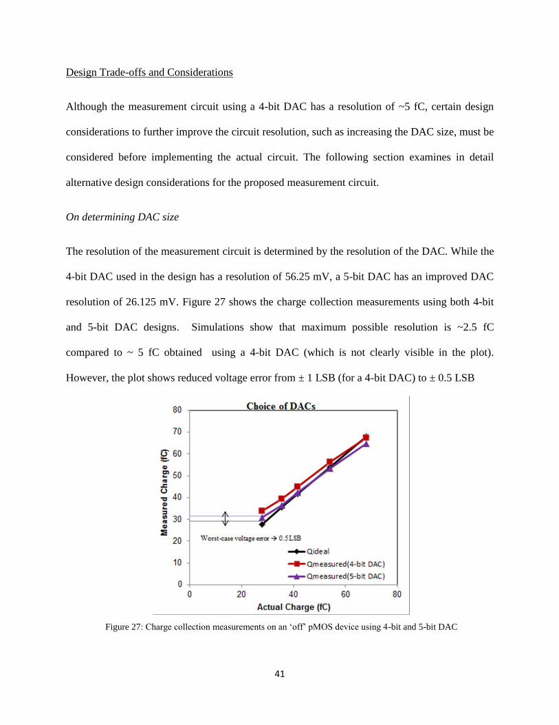
Although the measurement circuit using a 4-bit DAC has a resolution of ~5 fC, certain design
considerations to further improve the circuit resolution, such as increasing the DAC size, must be
considered before implementing the actual circuit. The following section examines in detail
alternative design considerations for the proposed measurement circuit.
On determining DAC size
The resolution of the measurement circuit is determined by the resolution of the DAC. While the
4-bit DAC used in the design has a resolution of 56.25 mV, a 5-bit DAC has an improved DAC
resolution of 26.125 mV. Figure 27 shows the charge collection measurements using both 4-bit
and 5-bit DAC designs. Simulations show that maximum possible resolution is ~2.5 fC
compared to ~ 5 fC obtained using a 4-bit DAC (which is not clearly visible in the plot).
However, the plot shows reduced voltage error from ± 1 LSB (for a 4-bit DAC) to ± 0.5 LSB
Figure 27: Charge collection measurements on an ‘off’ pMOS device using 4-bit and 5-bit DAC
42
(for a 5-bit DAC). Thus, implementing higher order DACs means higher resolution and reduced
voltage errors. But, there is an upper limit on the DAC size that could be used for the
measurement circuit which is primarily based on the accuracy at which the PDH circuit detects
and holds Vpeak. The maximum voltage error/ offset of the PDH circuit that exceeds 1 LSB (LSB
is a unit of DAC resolution) determines the maximum DAC size. Results show that for a PDH
circuit that is within ~ 20 mV of voltage offset, a 5-bit DAC would be the optimal DAC size for
implementing the charge measurement circuit.
On comparator design
Throughout this work, the circuit design involves two comparators i.e., one used in the design of
peak detect and hold circuit (PDH) design and the other to compare the detected peak voltage
against the DAC voltage. Since any voltage error induced in the charge collection measurement
is due to the non-idealities of these comparator designs, this section briefly analyzes the impact
of an ideal comparator design on the accuracy of charge collection measurements. Thus, the
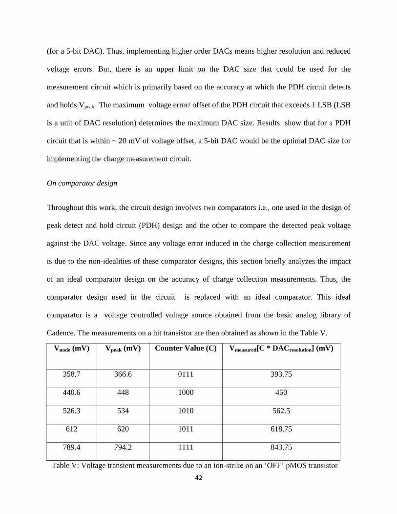
comparator design used in the circuit is replaced with an ideal comparator. This ideal
comparator is a voltage controlled voltage source obtained from the basic analog library of
Cadence. The measurements on a hit transistor are then obtained as shown in the Table V.
Vnode (mV) Vpeak (mV) Counter Value (C) Vmeasured[C * DACresolution] (mV)
358.7 366.6 0111 393.75
440.6 448 1000 450
526.3 534 1010 562.5
612 620 1011 618.75
789.4 794.2 1111 843.75
Table V: Voltage transient measurements due to an ion-strike on an ‘OFF’ pMOS transistor
43
From the table, it is observed that the worst-case voltage error is 1 LSB. Simulations using ideal
comparator suggests that by optimizing the comparator design, it is possible to improve the
circuit measurement resolution by implementing the circuit using higher order DAC. For
example in this case voltage droop due to the PDH circuit is 8 mV (as observed from the Table
V) and hence a 7-bit DAC (optimal size) could be implemented to allow a measurement
resolution of ~ 1.4 fC of charge (since 1 LSB for a 7-bit DAC = 14 mV).
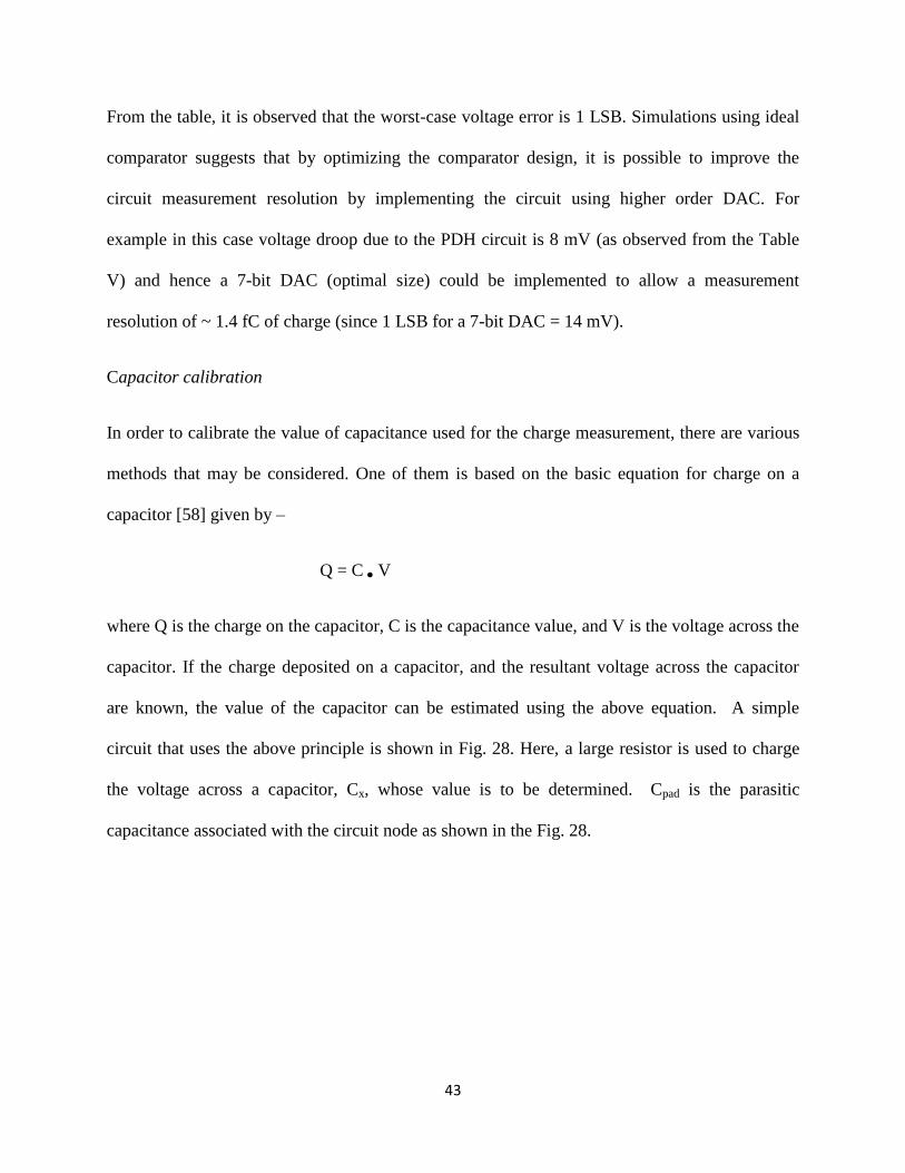
Capacitor calibration
In order to calibrate the value of capacitance used for the charge measurement, there are various
methods that may be considered. One of them is based on the basic equation for charge on a
capacitor [58] given by –
Q = C ● V
where Q is the charge on the capacitor, C is the capacitance value, and V is the voltage across the
capacitor. If the charge deposited on a capacitor, and the resultant voltage across the capacitor
are known, the value of the capacitor can be estimated using the above equation. A simple
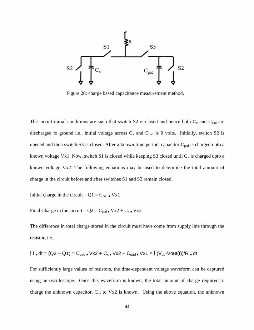
circuit that uses the above principle is shown in Fig. 28. Here, a large resistor is used to charge
the voltage across a capacitor, Cx, whose value is to be determined. Cpad is the parasitic
capacitance associated with the circuit node as shown in the Fig. 28.
44
The circuit initial conditions are such that switch S2 is closed and hence both Cx and Cpad are
discharged to ground i.e., initial voltage across Cx and Cpad is 0 volts. Initially, switch S2 is
opened and then switch S3 is closed. After a known time period, capacitor Cpad is charged upto a
known voltage Vx1. Now, switch S1 is closed while keeping S3 closed until Cx is charged upto a
known voltage Vx2. The following equations may be used to determine the total amount of
charge in the circuit before and after switches S1 and S3 remain closed.
Initial charge in the circuit – Q1 = Cpad ● Vx1
Final Charge in the circuit – Q2 = Cpad ● Vx2 + Cx ● Vx2
The difference in total charge stored in the circuit must have come from supply line through the
resistor, i.e.,
∫ I ● dt = (Q2 – Q1) = Cpad ● Vx2 + Cx ● Vx2 – Cpad ● Vx1 = ∫ (Vdd-Vout(t))/R ● dt
For sufficiently large values of resistors, the time-dependent voltage waveform can be captured
using an oscilloscope. Once this waveform is known, the total amount of charge required to
charge the unknown capacitor, Cx, to Vx2 is known. Using the above equation, the unknown
Figure 28: charge based capacitance measurement method.
45
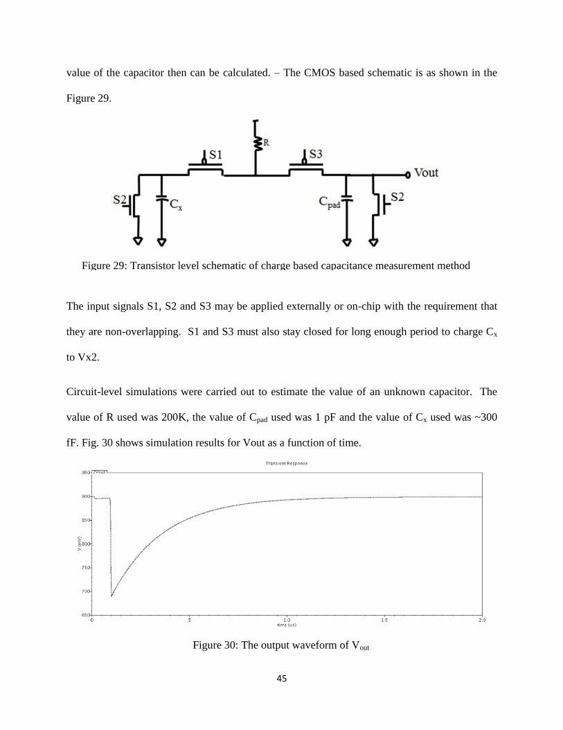
value of the capacitor then can be calculated. – The CMOS based schematic is as shown in the
Figure 29.
The input signals S1, S2 and S3 may be applied externally or on-chip with the requirement that
they are non-overlapping. S1 and S3 must also stay closed for long enough period to charge Cx
to Vx2.
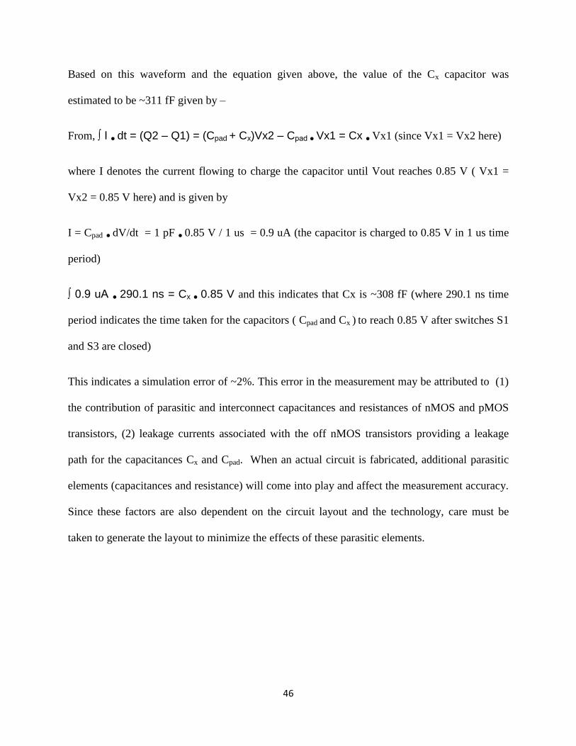
Circuit-level simulations were carried out to estimate the value of an unknown capacitor. The
value of R used was 200K, the value of Cpad used was 1 pF and the value of Cx used was ~300
fF. Fig. 30 shows simulation results for Vout as a function of time.
Figure 29: Transistor level schematic of charge based capacitance measurement method
Figure 30: The output waveform of Vout
46
Based on this waveform and the equation given above, the value of the Cx capacitor was
estimated to be ~311 fF given by –
From, ∫ I ● dt = (Q2 – Q1) = (Cpad + Cx)Vx2 – Cpad ● Vx1 = Cx ● Vx1 (since Vx1 = Vx2 here)
where I denotes the current flowing to charge the capacitor until Vout reaches 0.85 V ( Vx1 =
Vx2 = 0.85 V here) and is given by
I = Cpad ● dV/dt = 1 pF ● 0.85 V / 1 us = 0.9 uA (the capacitor is charged to 0.85 V in 1 us time
period)
∫ 0.9 uA ● 290.1 ns = Cx ● 0.85 V and this indicates that Cx is ~308 fF (where 290.1 ns time
period indicates the time taken for the capacitors ( Cpad and Cx ) to reach 0.85 V after switches S1
and S3 are closed)
This indicates a simulation error of ~2%. This error in the measurement may be attributed to (1)
the contribution of parasitic and interconnect capacitances and resistances of nMOS and pMOS
transistors, (2) leakage currents associated with the off nMOS transistors providing a leakage
path for the capacitances Cx and Cpad. When an actual circuit is fabricated, additional parasitic
elements (capacitances and resistance) will come into play and affect the measurement accuracy.
Since these factors are also dependent on the circuit layout and the technology, care must be
taken to generate the layout to minimize the effects of these parasitic elements.
47
CHAPTER V
CONCLUSION
This thesis describes the implementation of an autonomous charge collection measurement
circuit to experimentally characterize charge collection process in advanced technologies.
Simulations were performed using the UMC 40 nm process with SE strikes represented by the
double-exponential current pulse model. Results show a maximum measurement resolution of
~5 fC with a voltage offset of ± 1 LSB. For supply voltage variations of ~10% the circuit shows
a minimum voltage error of ± 1 LSB (where 1 LSB = 0.056 V (or) 5 fC) while its resolution still
remains 5 fC. Additionally for simulations carried out at different process corners to characterize
the circuit for process variations, its voltage offset varied from ± 1.4 LSB (at a ‘ss’ process
corner) to ± 1 LSB (for a ‘fnsp’ process corner).
Simulations to determine the optimal DAC size that could be used to improve the circuit
resolution indicated using a 5-bit DAC for a maximum ~ 2.5 fC resolution. Typically, laser or
broad beam experiments are carried out to test the circuit designs. For laser tests, the exact
location at which the hit takes place is known and hence the design could be tested using laser.
Also, the self-triggered circuit technique allows for one-time measurements due to ion-strikes on
circuit nodes. Another advantage with the circuit technique is that the voltage measurements are
such that user reads out a digital value corresponding to the voltage transient on the circuit node.
However, for broad beam experiments information regarding the time and location of the hit
node is usually not available and hence it is required that the target sensitive area be much larger

48
compared to the measurement circuit. Further improvements by considering target structures for
broad beam experiments are also possible.
49
REFERENCES
[1] R. C. Baumann, “Single event effects in advanced CMOS Technology,” in Proc. IEEE
Nuclear and Space Radiation Effects Conf. Short Course Text, 2005
[2] Critical Reliability Challenges for The International Technology Roadmap for
Semiconductors (ITRS), March 2003
[3] L. W. Massengill, “SEU modeling and prediction techniques,” in IEEE NSREC Short
Course, 1993, pp. III-1–III-93.
[4] M. E. Law, “Device modeling of single event effects,” in IEEE NSREC Short Course,
2006, pp. IV-1–IV-32.
[5] B. D. Olson, D. R. Ball, K. M. Warren, L. W. Massengill, N. F. Haddad, S. E. Doyle, and
D. McMorrow, “Simultaneous single event charge sharing and parasitic bipolar
conduction in a highly-scaled SRAM design,” IEEE Trans. Nucl. Sci., vol. 52, no. 6, pp.
2132–2136, Dec. 2005
[6] O. A. Amusan, A. F. Witulski, L. W. Massengill, B. L. Bhuva, P. R. Fleming, M. L.
Alles, A. L. Sternberg, J. D. Black, and R. D. Schrimpf, “Charge collection and charge
sharing in a 130 nm CMOS technology,” IEEE Trans. Nucl. Sci., vol. 53, no. 6, pp.
3253–3258, Dec. 2006
[7] E. Sun, J. Moll, J. Berger, and B. Alders, “Breakdown mechanism in short-channel MOS
transistors,” in Proc. Int. Electron Devices Meeting, Washington, D. C., 1978, pp. 478–
482
[8] J. S. Fu, C. L. Axness, and H. T. Weaver, “Memory SEU simulations using 2-D transport
calculations,” IEEE Electron. Device Lett., vol. 6, pp. 422–424, Aug. 1985
[9] R. L. Woodruff and P. J. Rudeck, “Three-dimensional numerical simulation of single
event upset of an SRAM cell,” IEEE Trans. Nucl. Sci., vol. 40, no. 6, pp. 1795–1803,
Dec. 1993
[10] B. D. Olson, O. A. Amusan, S. Dasgupta, L. W. Massengill, A. F.Witulski, B. L. Bhuva,
M. L. Alles, K. M. Warren, and D. R. Ball, “Analysis of parasitic bipolar transistor
mitigation using well contacts in 130 nm and 90 nm CMOS technology,” IEEE Trans.
Nucl. Sci., vol. 54, no. 4, pp. 894–897, Aug. 2007
[11] O. A. Amusan, L. W. Massengill, B. L. Bhuva, S. DasGupta, A. F. Witulski, and J. R.
Ahlbin, “Design techniques to reduce SET pulse widths in deep-submicron
combinational logic,” IEEE Trans. Nucl. Sci., vol. 54, no. 6, pp. 2060–2064, Dec. 2007
50
[12] E. Ibe, S. S. Chung, S. Wen, H. Yamaguchi, Y. Yahagi, H. Kameyama, S. Yamamoto,
and T. Akioka, “Spreading diversity in multi-cell neutron-induced upsets with device
scaling,” in Proc. IEEE Custom Integrated Circuits Conf., 2006, pp. 437–444
[13] Encyclopedia Britannica. [Online]. Available: http://www.britannica.com/ebc/art
632/The-Van-Allen-radiation-belts-contained-within-the-Earths-magnetosphere
[14] M. Xapsos, “Modeling the Space Radiation Environment,” presented at the 2006 IEEE
Nuclear and Space Radiation Effects Conference Short Course, Ponte Vedra Beach, FL
[15] A. Holmes-Siedle and L. Adams, “Radiation Environments,” in Handbook of Radiation
Effects, 2nd ed. New York: Oxford University Press Inc, 2002, ch. 2, pp. 17-26
[16] M. Xapsos, “Applicability of LET to Single Events in Microelectronic Structures,” IEEE
Trans. Nucl. Sci., vol. 39, no. 6, pp. 1613-1621, Dec. 1992.
[17] M. Xapsos, “The Shape of Heavy-Ion Upset Cross-Section Curves,” IEEE Trans. Nucl.
Sci., vol. 40, no. 6, pp. 1812-1819, Dec. 1993.
[18] S. Buchner and M. Baze, “Single- Event Transients in Fast Circuits,” presented at the
2001 IEEE Nuclear and Space Radiation Effects Conference Short Course, Vancouver,
BC, Canada
[19] J. F. Ziegler, J. P. Biersack, and U. Littmark, The Stopping and Range of Ions in Solids,
(Pergamon Press, New York, 1985).
[20] E. L. Petersen, “Single Event Analysis and Prediction,” 1997 IEEE NSREC Short
Course, Snowmass, CO.
[21] E. Petersen, “Soft errors due to protons in the radiation belt,” IEEE Trans. Nucl. Sci., vol.
28, pp. 3981–3986, Dec. 1981.
[22] F. Wrobel, J.-M. Palau, M. C. Calvet, O. Bersillon, and H. Duarte, “Incidence of multi-
particle events on soft error rates caused by n-Si nuclear reactions,” IEEE Trans. Nucl.
Sci., vol. 47, pp. 2580–2585, Dec. 2000.
[23] A. D. Tipton, J. A. Pellish, R. A. Reed, R. D. Schrimpf, R. A. Weller, M. H.
Mendenhall, B. Sierawski, A. K. Sutton, R. M. Diestelhorst, G. Espinel, J. D.
Cressler, P. W. Marshall, G. Vizkelethy, “Multiple-Bit Upset in 130 nm CMOS
Technology,” IEEE Trans. Nucl. Sci., vol. 53, no. 6, pp. 3259 – 3264, Dec. 2006.
[24] P. E. Dodd and L. W. Massengill “Basic Mechanisms and Modeling of Single Event
Upset in Digital Microelectronics,” IEEE Trans. Nucl. Sci., vol. 50, no. 3, June 2003.
51
[25] C. M. Hsieh, P. C. Murley, and R. R. O’Brien, “Dynamics of charge collection from
alpha-particle tracks in integrated circuits,” Proc. IEEE Int. Reliability Phys. Symp., pp.
38-42, 1981
[26] C. M. Hsieh, P. C. Murley, and R. R. O’Brien, “A field-funneling effect on the collection
of alpha-particle generated carriers in silicon devices,” IEEE Electron Device Lett., vol.
2, no. 4, pp. 103-105, 1981.
[27] C. M. Hsieh, P. C. Murley, and R. R. O’Brien, “Collection of charge from alpha-particle
tracks in silicon devices,” IEEE Trans. Electron Devices, vol. 30, no. 6, pp. 686-693,
1983.
[28] N. E. Islam, R. D. Pugh, C. P. Brothers, W. M. Shedd, B. K. Singaraju, J. W. Howard, Jr.,
H. Dussault, and O. Fageeha, “Basic mechanisms for enhanced prompt charge collection
in a n+p junction following single charged particle interaction,” J. Appl. Phys., vol. 84,
no. 5, pp. 2690-2696, 1998.
[29] P. E. Dodd, F. W. Sexton, and P. S. Winokur, “Three-dimensional simulation of charge
collection and multiple-bit upset in Si devices,” IEEE Trans. Nucl. Sci., vol. 41, no. 6, pp.
2005-2017, 1994.
[30] L. D. Edmonds, “Charge collection from ion tracks in simple EPI diodes,” IEEE Trans.
Nucl. Sci., vol. 44, no. 3, pp. 1448-1463, 1997.
[31] L. D. Edmonds, “Electric currents through ion tracks in silicon devices,” IEEE Trans.
Nucl. Sci., vol. 45, no. 6, pp. 3153-3164, 1998.
[32] S. E. Kerns, L. W. Massengill, D. V. Kerns, M. L. Alles, T. W. Houston, H. Lu, and L. R.
Hite, “Model for CMOS/SOI Single-Event Vulnerability,” IEEE Trans. On Nuclear
Science, vol. 36, pp. 2305-2310, Dec. 1989
[33] B. D. Olson, D. R. Ball, K. M. Warren, L. W. Massengill, N. F. Haddad, S. E. Doyle, and
D. McMorrow, “simultaneous single event charge sharing and parasitic bipolar
conduction in a highly-scaled SRAM design,” IEEE Trans. on Nuclear Science,
vol. 52, pp. 2132-2136, Dec. 2005
[34] A. W. Waskiewicz, J. W. Groninger, V. H. Strahan, and D. M. Long, “Burnout of power
MOS transistors with heavy ions of Californium-252,” IEEE Trans. Nucl. Sci., vol. 33,
no. 6, pp. 1710-1713, 1986.
[35] J. L. Titus, G. H. Johnson, R. D. Schrimpf, and K. F. Galloway, “Single-event burnout of
power bipolar junction transistors,” IEEE Trans. Nucl. Sci., vol. 38, no. 6, pp. 1315-1322,
1991.
[36] D. L. Oberg, J. L. Wert, E. Normand, P. P. Majewski, and S. A. Wender, “First
observations of power MOSFET burnout with high energy neutrons,” IEEE Trans. Nucl.
Sci., vol. 43, no. 6, pp. 2913-2920, 1996.
52
[37] J. W. Adolphsen, J. L. Barth, and G. B. Gee, “First observation of proton induced power
MOSFET burnout in space: The CRUX experiment on APEX,” IEEE Trans. Nucl. Sci.,
vol. 43, no. 6, pp. 2921-2926, 1996.
[38] S. Kuboyama, K. Sugimoto, S. Shugyo, S. Matsuda, and T. Hirao, “Single-event burnout
of epitaxial bipolar transistors,” IEEE Trans. Nucl. Sci., vol. 45, no. 6, pp. 2527-2533,
1998.
[39] G. M. Swift, D. J. Padgett, and A. H. Johnston, “A new class of single event hard errors,”
IEEE Trans. Nucl. Sci., vol. 41, no. 6, pp. 2043-2048, 1994
[40] F. W. Sexton, D. M. Fleetwood, M. R. Shaneyfelt, P. E. Dodd, and G. L. Hash, “Single
event gate rupture in thin gate oxides,” IEEE Trans. Nucl. Sci., vol. 44, no. 6, pp. 2345-
2352, 1997.
[41] F. W. Sexton, D. M. Fleetwood, M. R. Shaneyfelt, P. E. Dodd, G. L. Hash, L. P.
Schanwald, R. A. Loemker, K. S. Krisch, M. L. Green, B. E. Weir, and P. J. Silverman,
“Precursor ion damage and angular dependence of single event gate rupture in thin
oxides,” IEEE Trans. Nucl. Sci., vol. 45, no. 6, pp. 2509-2518, 1998.
[42] A. H. Johnston, “The influence of VLSI technology evolution on radiation-induced
latchup in space systems,” IEEE Trans. Nucl. Sci., vol. 43, no. 2, pp. 505-521, 1996
[43] M. B. H. Breese, E. Vittone, G. Vizkelethy, and P. J. Sellin, “A review of ion beam
induced charge microscopy,” Nucl. Instrum. Meth. Phys. Res. B, vol. 264, no. 2, pp. 345–
360, Nov. 2007
[44] S. DasGupta, A. F. Witulski, B. Bhuva, M. Alles, R. A. Reed, O. A. Amusan, J. R.
Ahlbin, R. Schrimpf, and L. W. Massengill, “Effect of well and substrate potential
modulation on single event pulse shape in deep submicron CMOS,” IEEE Trans. Nucl.
Sci., vol. 54, no. 6, pp. 2407–2412, Dec. 2007
[45] O. A. Amusan, P. R. Fleming, B. L. Bhuva, L. W. Massengill, A. F. Witulski, M. C.
Casey, D. McMorrow, S. A. Nation, F. Barsun, J. S. Melinger, M. J. Gadlage, and T. D.
Loveless, “Laser verification of on-chip charge collection measurement circuit,” IEEE
Trans. Nucl. Sci., vol. 55, pp. 3309–3313, Dec. 2008
[46] P. F. Buckens and M. S. Veatch, "A high performance peak-detect& hold circuit for pulse
height analysis," IEEE Trans. Nucl. Sci.,vol. 39 (4), pp 753-757 ( 1992)
[47] M. W. Kruiskamp and D. M. W. Leenaerts, “A CMOS peak detect sample and hold
circuit,” IEEE Trans. Nucl. Sci., vol. 41, no. 1, pp. 295–298, Feb. 1994
53
[48] L. Fabris, P.G. Allen, J.J. Bucher, N.M. Edelstein, D.A. Landis, N.W. Madden, D.K.
Shuh, Fast peak detector stretchers for use in XAFS applications, Proceedings of the
IEEE Nuclear Science Symposium (NSS’98), Toronto, Canada, November 1998.
[49] K. Koli, K. Halonen, Low voltage MOS-transistor-only precision current peak detector
with signal independent discharge time constant, Proceedings of the IEEE International
Symposium on Circuits and Systems (ISCAS’97), Hong Kong, June 1997.
[50] B. Razavi and B. W. Wooley, “Design techniques for high-speed, high-resolution
comparators.” IEEE J . Solid-state Circuit.s, vol. 27, pp. 1916-1992, Dec. 1992
[51] Cadence Spectre Circuit Simulator User Guide, Sept. 2003
[52] Jeffrey S. Kauppila, A. L. Sternberg, M. L. Alles, A. M. Francis, J. Holmes, O. A.
Amusan, and L. W. Massengill, “A Bias-Dependent Single-Event Compact Model
Implemented Into BSIM4 and a 90 nm CMOS Process Design Kit” IEEE Trans. Nucl.
Sci. vol. 56 no. 6, pp. 3152-3157, Dec. 2009
[53] N. D. Arora, E. Rios, and C.-L. Huag, “Modeling the polysilicon depletion effect and its
impact on submicrometer CMOS circuit performance,” IEEE Trans. Electron Devices,
vol. 42, no. 5, pp. 935–943, May 1995
[54] J. Shyu, G. C. Temes, and F. Krummenacher, “Random error effects in matched MOS
capacitors and current sources,” IEEE J. Solid-State Circuits, vol. 19, no. 6, pp. 948–956,
Dec. 1984
[55] A. Asenov, S. Kaya, and A. R. Brown, “Intrinsic parameter fluctuations in
decananometer MOSFETS introduced by gate line edge roughness,” IEEE Trans.
Electron Devices, vol. 50, no. 5, pp. 1254–1260, May 2003
[56] P. A. Stolk, F. P. Widdershoven, and D. B. M. Klaasen, “Modeling statistical dopant
fluctuations in MOS transistors,” IEEE Trans. Electron Devices, vol. 45, no. 9, pp. 1960–
1971, Sep. 1998
[57] S. Borkar, “Designing reliable systems from unreliable components: The challenges of
transistor variability and degradation,” IEEE Micro, vol. 25, no. 6, pp. 10–16, Nov.–Dec.
2005
[58] J. C. Chen, B. W. McGaughy, D. Sylvester, and C. Hu, “An on-chip, attofarad
interconnect Charge-Based Capacitance Measurement (CBCM) technique,” in IEDM
Tech. Dig., 1996, pp. 69–72.
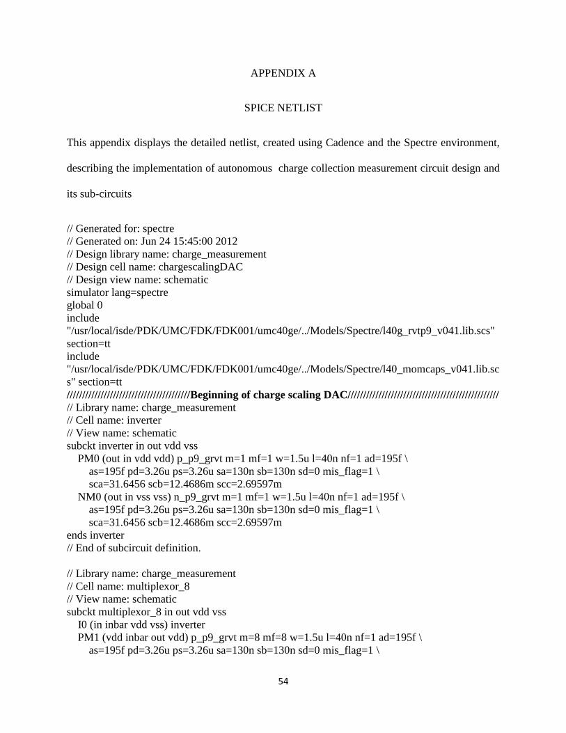
54
APPENDIX A
SPICE NETLIST
This appendix displays the detailed netlist, created using Cadence and the Spectre environment,
describing the implementation of autonomous charge collection measurement circuit design and
its sub-circuits
// Generated for: spectre
// Generated on: Jun 24 15:45:00 2012
// Design library name: charge_measurement
// Design cell name: chargescalingDAC
// Design view name: schematic
simulator lang=spectre
global 0
include
"/usr/local/isde/PDK/UMC/FDK/FDK001/umc40ge/../Models/Spectre/l40g_rvtp9_v041.lib.scs"
section=tt
include
"/usr/local/isde/PDK/UMC/FDK/FDK001/umc40ge/../Models/Spectre/l40_momcaps_v041.lib.sc
s" section=tt
////////////////////////////////////////Beginning of charge scaling DAC/////////////////////////////////////////////////
// Library name: charge_measurement
// Cell name: inverter
// View name: schematic
subckt inverter in out vdd vss
PM0 (out in vdd vdd) p_p9_grvt m=1 mf=1 w=1.5u l=40n nf=1 ad=195f \
as=195f pd=3.26u ps=3.26u sa=130n sb=130n sd=0 mis_flag=1 \
sca=31.6456 scb=12.4686m scc=2.69597m
NM0 (out in vss vss) n_p9_grvt m=1 mf=1 w=1.5u l=40n nf=1 ad=195f \
as=195f pd=3.26u ps=3.26u sa=130n sb=130n sd=0 mis_flag=1 \
sca=31.6456 scb=12.4686m scc=2.69597m
ends inverter
// End of subcircuit definition.
// Library name: charge_measurement
// Cell name: multiplexor_8
// View name: schematic
subckt multiplexor_8 in out vdd vss
I0 (in inbar vdd vss) inverter
PM1 (vdd inbar out vdd) p_p9_grvt m=8 mf=8 w=1.5u l=40n nf=1 ad=195f \
as=195f pd=3.26u ps=3.26u sa=130n sb=130n sd=0 mis_flag=1 \
55
sca=31.6456 scb=12.4686m scc=2.69597m
PM0 (vss in out vdd) p_p9_grvt m=1 mf=1 w=4.005u l=40n nf=3 ad=360.45f \
as=360.45f pd=5.88u ps=5.88u sa=130n sb=130n sd=140n mis_flag=1 \
sca=35.3357 scb=13.9568m scc=3.02914m
NM1 (out in vdd vss) n_p9_grvt m=1 mf=1 w=1.5u l=40n nf=1 ad=195f \
as=195f pd=3.26u ps=3.26u sa=130n sb=130n sd=0 mis_flag=1 \
sca=31.6456 scb=12.4686m scc=2.69597m
NM0 (out inbar vss vss) n_p9_grvt m=8 mf=8 w=1.5u l=40n nf=1 ad=195f \
as=195f pd=3.26u ps=3.26u sa=130n sb=130n sd=0 mis_flag=1 \
sca=31.6456 scb=12.4686m scc=2.69597m
ends multiplexor_8
// End of subcircuit definition.
// Library name: charge_measurement
// Cell name: multiplexor_4
// View name: schematic
subckt multiplexor_4 in out vdd vss
I0 (in inbar vdd vss) inverter
PM1 (vdd inbar out vdd) p_p9_grvt m=4 mf=4 w=1.5u l=40n nf=1 ad=195f \
as=195f pd=3.26u ps=3.26u sa=130n sb=130n sd=0 mis_flag=1 \
sca=31.6456 scb=12.4686m scc=2.69597m
PM0 (vss in out vdd) p_p9_grvt m=1 mf=1 w=4.005u l=40n nf=3 ad=360.45f \
as=360.45f pd=5.88u ps=5.88u sa=130n sb=130n sd=140n mis_flag=1 \
sca=35.3357 scb=13.9568m scc=3.02914m
NM1 (out in vdd vss) n_p9_grvt m=1 mf=1 w=1.5u l=40n nf=1 ad=195f \
as=195f pd=3.26u ps=3.26u sa=130n sb=130n sd=0 mis_flag=1 \
sca=31.6456 scb=12.4686m scc=2.69597m
NM0 (out inbar vss vss) n_p9_grvt m=4 mf=4 w=1.5u l=40n nf=1 ad=195f \
as=195f pd=3.26u ps=3.26u sa=130n sb=130n sd=0 mis_flag=1 \
sca=31.6456 scb=12.4686m scc=2.69597m
ends multiplexor_4
// End of subcircuit definition.
// Library name: charge_measurement
// Cell name: multiplexor_2
// View name: schematic
subckt multiplexor_2 in out vdd vss
I0 (in inbar vdd vss) inverter
PM1 (vdd inbar out vdd) p_p9_grvt m=2 mf=2 w=1.5u l=40n nf=1 ad=195f \
as=195f pd=3.26u ps=3.26u sa=130n sb=130n sd=0 mis_flag=1 \
sca=31.6456 scb=12.4686m scc=2.69597m
PM0 (vss in out vdd) p_p9_grvt m=1 mf=1 w=4.005u l=40n nf=3 ad=360.45f \
as=360.45f pd=5.88u ps=5.88u sa=130n sb=130n sd=140n mis_flag=1 \
sca=35.3357 scb=13.9568m scc=3.02914m
NM1 (out in vdd vss) n_p9_grvt m=1 mf=1 w=1.5u l=40n nf=1 ad=195f \
as=195f pd=3.26u ps=3.26u sa=130n sb=130n sd=0 mis_flag=1 \
56
sca=31.6456 scb=12.4686m scc=2.69597m
NM0 (out inbar vss vss) n_p9_grvt m=2 mf=2 w=1.5u l=40n nf=1 ad=195f \
as=195f pd=3.26u ps=3.26u sa=130n sb=130n sd=0 mis_flag=1 \
sca=31.6456 scb=12.4686m scc=2.69597m
ends multiplexor_2
// End of subcircuit definition.
// Library name: charge_measurement
// Cell name: multiplexor
// View name: schematic
subckt multiplexor in out vdd vss
I0 (in inbar vdd vss) inverter
PM1 (vdd inbar out vdd) p_p9_grvt m=1 mf=1 w=1.5u l=40n nf=1 ad=195f \
as=195f pd=3.26u ps=3.26u sa=130n sb=130n sd=0 mis_flag=1 \
sca=31.6456 scb=12.4686m scc=2.69597m
PM0 (vss in out vdd) p_p9_grvt m=1 mf=1 w=4.005u l=40n nf=3 ad=360.45f \
as=360.45f pd=5.88u ps=5.88u sa=130n sb=130n sd=140n mis_flag=1 \
sca=35.3357 scb=13.9568m scc=3.02914m
NM1 (out in vdd vss) n_p9_grvt m=1 mf=1 w=1.5u l=40n nf=1 ad=195f \
as=195f pd=3.26u ps=3.26u sa=130n sb=130n sd=0 mis_flag=1 \
sca=31.6456 scb=12.4686m scc=2.69597m
NM0 (out inbar vss vss) n_p9_grvt m=1 mf=1 w=1.5u l=40n nf=1 ad=195f \
as=195f pd=3.26u ps=3.26u sa=130n sb=130n sd=0 mis_flag=1 \
sca=31.6456 scb=12.4686m scc=2.69597m
ends multiplexor
// End of subcircuit definition.
// Library name: charge_measurement
// Cell name: chargescalingDAC
// View name: schematic
V0 (vactual vss) vsource type=pwl wave=[ 2.25n 0 2.75n 56m 3.25n 112.5m \
3.75n 168m 4.25n 225m 4.75n 281.25m 5.25n 337.5m 5.75n 393.75m \
6.25n 450m 6.75n 506.25m 7.25n 562.5m 7.75n 618.75m 8.25n 675m \
8.75n 731.25m 9.25n 787.5m 9.75n 843.75m ]
I0 (i3 net29 vdd vss) multiplexor_8
I5 (i2 net25 vdd vss) multiplexor_4
I10 (i1 net17 vdd vss) multiplexor_2
C17 (vout net17 vss) momcaps_as_mmkf l=16.17u nf=13 nm=4 bm=1 m=2 \
mis_flag=1 metal_ring_flag=1 presim_flag=1
C18 (vout net25 vss) momcaps_as_mmkf l=16.17u nf=13 nm=4 bm=1 m=4 \
mis_flag=1 metal_ring_flag=1 presim_flag=1
C20 (vout net29 vss) momcaps_as_mmkf l=16.17u nf=13 nm=4 bm=1 m=8 \
mis_flag=1 metal_ring_flag=1 presim_flag=1
C1 (vout net21 vss) momcaps_as_mmkf l=16.17u nf=13 nm=4 bm=1 m=1 \
mis_flag=1 metal_ring_flag=1 presim_flag=1
C0 (vout vss) capacitor c=50f
57
NM0 (vout vreset vss vss) n_p9_grvt m=1 mf=1 w=1.5u l=40n nf=1 ad=195f \
as=195f pd=3.26u ps=3.26u sa=130n sb=130n sd=0 mis_flag=1 \
sca=31.6456 scb=12.4686m scc=2.69597m
I6 (i0 net21 vdd vss) multiplexor
include "./_graphical_stimuli.scs"
simulatorOptions options reltol=1e-3 vabstol=1e-6 iabstol=1e-12 temp=27 \
tnom=25 scalem=1.0 scale=1.0 gmin=1e-12 rforce=1 maxnotes=5 maxwarns=5 \
digits=5 cols=80 pivrel=1e-3 sensfile="../psf/sens.output" \
checklimitdest=psf
tran tran stop=10n write="spectre.ic" writefinal="spectre.fc" \
annotate=status maxiters=5
finalTimeOP info what=oppoint where=rawfile
modelParameter info what=models where=rawfile
element info what=inst where=rawfile
outputParameter info what=output where=rawfile
designParamVals info what=parameters where=rawfile
primitives info what=primitives where=rawfile
subckts info what=subckts where=rawfile
saveOptions options save=allpub
//////////////////////////////////////////End of charge scaling DAC////////////////////////////////////////////////////////
// Generated for: spectre
// Generated on: May 24 11:20:13 2012
// Design library name: charge_measurement
// Design cell name: 4bit_sync_counter
// Design view name: schematic
simulator lang=spectre
global 0
include
"/usr/local/isde/PDK/UMC/FDK/FDK001/umc40ge/../Models/Spectre/l40g_rvtp9_v041.lib.scs"
section=ff
////////////////////////////////////////Beginning of 4-bit counter////////////////////////////////////////////////////////////
// Library name: charge_measurement
// Cell name: inverter
// View name: schematic
subckt inverter in out vdd vss
PM0 (out in vdd vdd) p_p9_grvt m=1 mf=1 w=1.5u l=40n nf=1 ad=195f \
as=195f pd=3.26u ps=3.26u sa=130n sb=130n sd=0 mis_flag=1 \
sca=31.6456 scb=12.4686m scc=2.69597m
NM0 (out in vss vss) n_p9_grvt m=1 mf=1 w=1.5u l=40n nf=1 ad=195f \
as=195f pd=3.26u ps=3.26u sa=130n sb=130n sd=0 mis_flag=1 \
sca=31.6456 scb=12.4686m scc=2.69597m
ends inverter
// End of subcircuit definition.
58
// Library name: charge_measurement
// Cell name: nand
// View name: schematic
subckt nand a b out vdd vss
PM1 (out b vdd vdd) p_p9_grvt m=1 mf=1 w=1.5u l=40n nf=1 ad=195f \
as=195f pd=3.26u ps=3.26u sa=130n sb=130n sd=0 mis_flag=1 \
sca=31.6456 scb=12.4686m scc=2.69597m
PM0 (out a vdd vdd) p_p9_grvt m=1 mf=1 w=1.5u l=40n nf=1 ad=195f \
as=195f pd=3.26u ps=3.26u sa=130n sb=130n sd=0 mis_flag=1 \
sca=31.6456 scb=12.4686m scc=2.69597m
NM0 (net14 b vss vss) n_p9_grvt m=1 mf=1 w=1.5u l=40n nf=1 ad=195f \
as=195f pd=3.26u ps=3.26u sa=130n sb=130n sd=0 mis_flag=1 \
sca=31.6456 scb=12.4686m scc=2.69597m
NM1 (out a net14 vss) n_p9_grvt m=1 mf=1 w=1.5u l=40n nf=1 ad=195f \
as=195f pd=3.26u ps=3.26u sa=130n sb=130n sd=0 mis_flag=1 \
sca=31.6456 scb=12.4686m scc=2.69597m
ends nand
// End of subcircuit definition.
// Library name: charge_measurement
// Cell name: nand3
// View name: schematic
subckt nand3 a b c out vdd vss
NM2 (net7 c vss vss) n_p9_grvt m=1 mf=1 w=1.5u l=40n nf=1 ad=195f \
as=195f pd=3.26u ps=3.26u sa=130n sb=130n sd=0 mis_flag=1 \
sca=31.6456 scb=12.4686m scc=2.69597m
NM1 (out a net15 vss) n_p9_grvt m=1 mf=1 w=1.5u l=40n nf=1 ad=195f \
as=195f pd=3.26u ps=3.26u sa=130n sb=130n sd=0 mis_flag=1 \
sca=31.6456 scb=12.4686m scc=2.69597m
NM0 (net15 b net7 vss) n_p9_grvt m=1 mf=1 w=1.5u l=40n nf=1 ad=195f \
as=195f pd=3.26u ps=3.26u sa=130n sb=130n sd=0 mis_flag=1 \
sca=31.6456 scb=12.4686m scc=2.69597m
PM2 (out a vdd vdd) p_p9_grvt m=1 mf=1 w=1.5u l=40n nf=1 ad=195f \
as=195f pd=3.26u ps=3.26u sa=130n sb=130n sd=0 mis_flag=1 \
sca=31.6456 scb=12.4686m scc=2.69597m
PM0 (out b vdd vdd) p_p9_grvt m=1 mf=1 w=1.5u l=40n nf=1 ad=195f \
as=195f pd=3.26u ps=3.26u sa=130n sb=130n sd=0 mis_flag=1 \
sca=31.6456 scb=12.4686m scc=2.69597m
PM1 (out c vdd vdd) p_p9_grvt m=1 mf=1 w=1.5u l=40n nf=1 ad=195f \
as=195f pd=3.26u ps=3.26u sa=130n sb=130n sd=0 mis_flag=1 \
sca=31.6456 scb=12.4686m scc=2.69597m
ends nand3
// End of subcircuit definition.
// Library name: charge_measurement
// Cell name: Tff_clear
59
// View name: schematic
subckt Tff_clear Q Q0 T clear clock vdd vss
I10 (clock clockb vdd vss) inverter
I8 (net24 Q0 Q vdd vss) nand
I7 (clockb net27 net19 vdd vss) nand
I6 (net40 clockb net24 vdd vss) nand
I4 (net53 net27 net40 vdd vss) nand
I9 (Q net19 clear Q0 vdd vss) nand3
I5 (net40 net47 clear net27 vdd vss) nand3
I3 (T clock Q net47 vdd vss) nand3
I2 (Q0 clock T net53 vdd vss) nand3
ends Tff_clear
// End of subcircuit definition.
// Library name: charge_measurement
// Cell name: 4bit_sync_counter
// View name: schematic
I12 (net10 net11 vdd vss) inverter
I10 (net14 net45 vdd vss) inverter
I7 (net34 net19 vdd vss) inverter
I13 (out2 net45 net10 vdd vss) nand
I11 (out1 net19 net14 vdd vss) nand
I4 (enable_high out0 net34 vdd vss) nand
I3 (out3 net39 net11 clear_activelow clock vdd vss) Tff_clear
I2 (out2 net46 net45 clear_activelow clock vdd vss) Tff_clear
I1 (out1 net53 net19 clear_activelow clock vdd vss) Tff_clear
I0 (out0 net60 enable_high clear_activelow clock vdd vss) Tff_clear
include "./_graphical_stimuli.scs"
simulatorOptions options reltol=1e-3 vabstol=1e-6 iabstol=1e-12 temp=27 \
tnom=25 scalem=1.0 scale=1.0 gmin=1e-12 rforce=1 maxnotes=5 maxwarns=5 \
digits=5 cols=80 pivrel=1e-3 sensfile="../psf/sens.output" \
checklimitdest=psf
tran tran stop=16n write="spectre.ic" writefinal="spectre.fc" \
annotate=status maxiters=5
finalTimeOP info what=oppoint where=rawfile
modelParameter info what=models where=rawfile
element info what=inst where=rawfile
outputParameter info what=output where=rawfile
designParamVals info what=parameters where=rawfile
primitives info what=primitives where=rawfile
subckts info what=subckts where=rawfile
saveOptions options save=allpub
//////////////////////////////////////////End of charge scaling DAC////////////////////////////////////////////////////////
// Generated for: spectre
// Generated on: Jun 24 15:48:35 2012
60
// Design library name: charge_measurement
// Design cell name: PeakDetector
// Design view name: schematic
simulator lang=spectre
global 0
include
"/usr/local/isde/PDK/UMC/FDK/FDK001/umc40ge/../Models/Spectre/l40g_hvtp9_v041.lib.scs"
section=tt
include
"/usr/local/isde/PDK/UMC/FDK/FDK001/umc40ge/../Models/Spectre/l40g_lvtp9_v041.lib.scs"
section=tt
include
"/usr/local/isde/PDK/UMC/FDK/FDK001/umc40ge/../Models/Spectre/l40g_rvtp9_v041.lib.scs"
section=tt
include
"/usr/local/isde/PDK/UMC/FDK/FDK001/umc40ge/../Models/Spectre/l40_momcaps_v041.lib.sc
s" section=tt
////////////////////////////////////////Beginning of peak detector///////////////////////////////////////////////////////////
// Library name: charge_measurement
// Cell name: PeakDetector
// View name: schematic
PM2 (vout net0121 vdd vdd) p_p9_ghvt m=1 mf=1 w=1.5u l=40n nf=1 ad=195f \
as=195f pd=3.26u ps=3.26u sa=130n sb=130n sd=0 mis_flag=1 \
sca=31.6456 scb=12.4686m scc=2.69597m
PM3 (net0121 net0121 vdd vdd) p_p9_ghvt m=1 mf=1 w=1.5u l=40n nf=1 ad=195f \
as=195f pd=3.26u ps=3.26u sa=130n sb=130n sd=0 mis_flag=1 \
sca=31.6456 scb=12.4686m scc=2.69597m
NM2 (vout vreset vss vss) n_p9_ghvt m=1 mf=1 w=200n l=40n nf=1 ad=26f \
as=26f pd=660n ps=660n sa=130n sb=130n sd=0 mis_flag=1 sca=178.571 \
scb=34.6615m scc=14.4428m
C0 (vout vss vss) momcaps_sy_mmkf l=5u nf=10 nm=3 bm=1 m=9 mis_flag=1 \
metal_ring_flag=1 shielding_flag=0 presim_flag=1
NM0 (net13 vpeak vss vss) n_p9_grvt m=1 mf=1 w=655n l=230n nf=1 ad=85.15f \
as=85.15f pd=1.57u ps=1.57u sa=130n sb=130n sd=0 mis_flag=1 \
sca=68.0272 scb=25.0363m scc=6.13303m
NM1 (net17 vout vss vss) n_p9_grvt m=1 mf=1 w=655n l=230n nf=1 ad=85.15f \
as=85.15f pd=1.57u ps=1.57u sa=130n sb=130n sd=0 mis_flag=1 \
sca=68.0272 scb=25.0363m scc=6.13303m
NM5 (net21 net25 vss vss) n_p9_grvt m=1 mf=1 w=655n l=50n nf=1 ad=85.15f \
as=85.15f pd=1.57u ps=1.57u sa=130n sb=130n sd=0 mis_flag=1 \
sca=68.0272 scb=25.0363m scc=6.13303m
NM4 (net25 net25 vss vss) n_p9_grvt m=1 mf=1 w=655n l=50n nf=1 ad=85.15f \
as=85.15f pd=1.57u ps=1.57u sa=130n sb=130n sd=0 mis_flag=1 \
sca=68.0272 scb=25.0363m scc=6.13303m
NM6 (net0121 net21 vss vss) n_p9_grvt m=1 mf=1 w=400n l=230n nf=1 ad=52f \
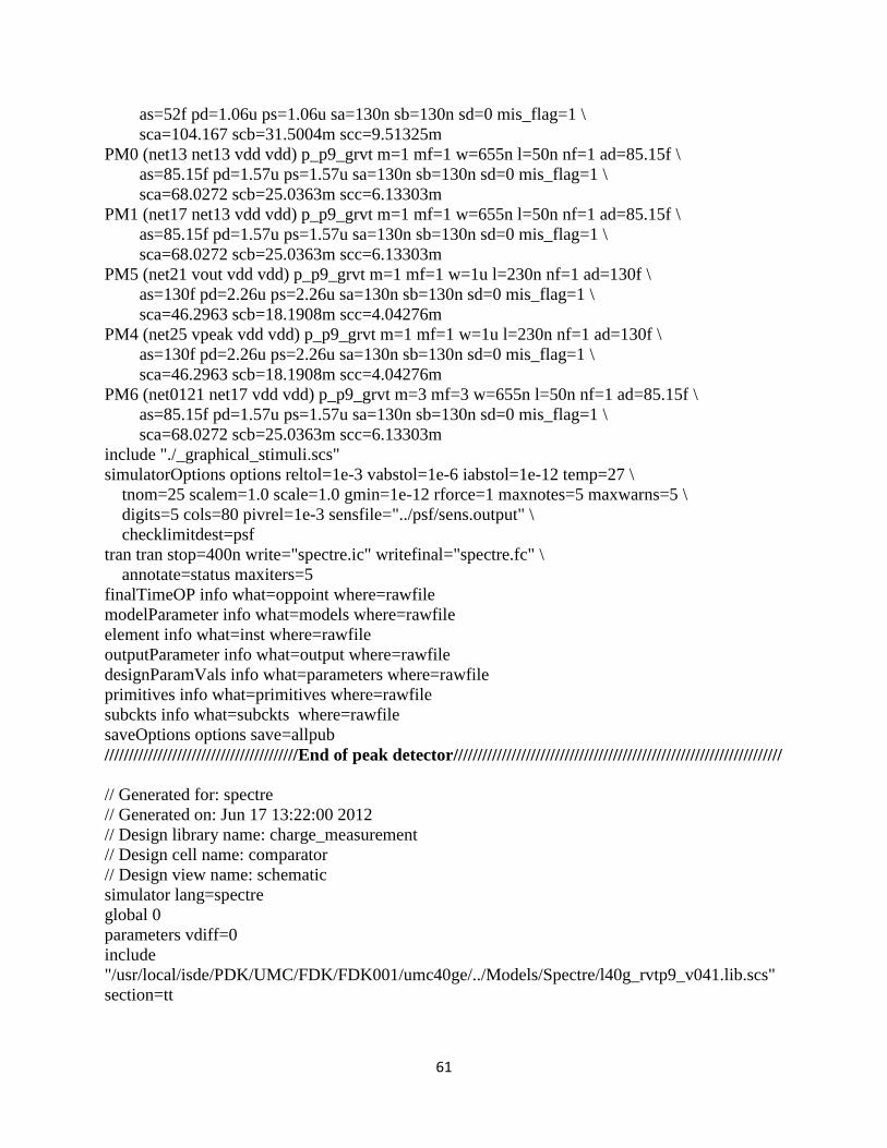
61
as=52f pd=1.06u ps=1.06u sa=130n sb=130n sd=0 mis_flag=1 \
sca=104.167 scb=31.5004m scc=9.51325m
PM0 (net13 net13 vdd vdd) p_p9_grvt m=1 mf=1 w=655n l=50n nf=1 ad=85.15f \
as=85.15f pd=1.57u ps=1.57u sa=130n sb=130n sd=0 mis_flag=1 \
sca=68.0272 scb=25.0363m scc=6.13303m
PM1 (net17 net13 vdd vdd) p_p9_grvt m=1 mf=1 w=655n l=50n nf=1 ad=85.15f \
as=85.15f pd=1.57u ps=1.57u sa=130n sb=130n sd=0 mis_flag=1 \
sca=68.0272 scb=25.0363m scc=6.13303m
PM5 (net21 vout vdd vdd) p_p9_grvt m=1 mf=1 w=1u l=230n nf=1 ad=130f \
as=130f pd=2.26u ps=2.26u sa=130n sb=130n sd=0 mis_flag=1 \
sca=46.2963 scb=18.1908m scc=4.04276m
PM4 (net25 vpeak vdd vdd) p_p9_grvt m=1 mf=1 w=1u l=230n nf=1 ad=130f \
as=130f pd=2.26u ps=2.26u sa=130n sb=130n sd=0 mis_flag=1 \
sca=46.2963 scb=18.1908m scc=4.04276m
PM6 (net0121 net17 vdd vdd) p_p9_grvt m=3 mf=3 w=655n l=50n nf=1 ad=85.15f \
as=85.15f pd=1.57u ps=1.57u sa=130n sb=130n sd=0 mis_flag=1 \
sca=68.0272 scb=25.0363m scc=6.13303m
include "./_graphical_stimuli.scs"
simulatorOptions options reltol=1e-3 vabstol=1e-6 iabstol=1e-12 temp=27 \
tnom=25 scalem=1.0 scale=1.0 gmin=1e-12 rforce=1 maxnotes=5 maxwarns=5 \
digits=5 cols=80 pivrel=1e-3 sensfile="../psf/sens.output" \
checklimitdest=psf
tran tran stop=400n write="spectre.ic" writefinal="spectre.fc" \
annotate=status maxiters=5
finalTimeOP info what=oppoint where=rawfile
modelParameter info what=models where=rawfile
element info what=inst where=rawfile
outputParameter info what=output where=rawfile
designParamVals info what=parameters where=rawfile
primitives info what=primitives where=rawfile
subckts info what=subckts where=rawfile
saveOptions options save=allpub
////////////////////////////////////////End of peak detector////////////////////////////////////////////////////////////////////
// Generated for: spectre
// Generated on: Jun 17 13:22:00 2012
// Design library name: charge_measurement
// Design cell name: comparator
// Design view name: schematic
simulator lang=spectre
global 0
parameters vdiff=0
include
"/usr/local/isde/PDK/UMC/FDK/FDK001/umc40ge/../Models/Spectre/l40g_rvtp9_v041.lib.scs"
section=tt
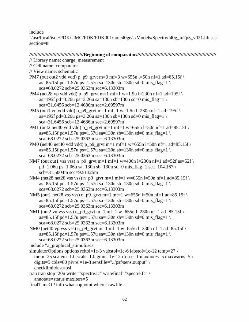
62
include
"/usr/local/isde/PDK/UMC/FDK/FDK001/umc40ge/../Models/Spectre/l40g_io2p5_v021.lib.scs"
section=tt
////////////////////////////////////////Beginning of comparator///////////////////////////////////////////////////////////
// Library name: charge_measurement
// Cell name: comparator
// View name: schematic
PM7 (out out2 vdd vdd) p_p9_grvt m=3 mf=3 w=655n l=50n nf=1 ad=85.15f \
as=85.15f pd=1.57u ps=1.57u sa=130n sb=130n sd=0 mis_flag=1 \
sca=68.0272 scb=25.0363m scc=6.13303m
PM4 (net28 vp vdd vdd) p_p9_grvt m=1 mf=1 w=1.5u l=230n nf=1 ad=195f \
as=195f pd=3.26u ps=3.26u sa=130n sb=130n sd=0 mis_flag=1 \
sca=31.6456 scb=12.4686m scc=2.69597m
PM5 (out1 vn vdd vdd) p_p9_grvt m=1 mf=1 w=1.5u l=230n nf=1 ad=195f \
as=195f pd=3.26u ps=3.26u sa=130n sb=130n sd=0 mis_flag=1 \
sca=31.6456 scb=12.4686m scc=2.69597m
PM1 (out2 net40 vdd vdd) p_p9_grvt m=1 mf=1 w=655n l=50n nf=1 ad=85.15f \
as=85.15f pd=1.57u ps=1.57u sa=130n sb=130n sd=0 mis_flag=1 \
sca=68.0272 scb=25.0363m scc=6.13303m
PM0 (net40 net40 vdd vdd) p_p9_grvt m=1 mf=1 w=655n l=50n nf=1 ad=85.15f \
as=85.15f pd=1.57u ps=1.57u sa=130n sb=130n sd=0 mis_flag=1 \
sca=68.0272 scb=25.0363m scc=6.13303m
NM7 (out out1 vss vss) n_p9_grvt m=1 mf=1 w=400n l=230n nf=1 ad=52f as=52f \
pd=1.06u ps=1.06u sa=130n sb=130n sd=0 mis_flag=1 sca=104.167 \
scb=31.5004m scc=9.51325m
NM4 (net28 net28 vss vss) n_p9_grvt m=1 mf=1 w=655n l=50n nf=1 ad=85.15f \
as=85.15f pd=1.57u ps=1.57u sa=130n sb=130n sd=0 mis_flag=1 \
sca=68.0272 scb=25.0363m scc=6.13303m
NM5 (out1 net28 vss vss) n_p9_grvt m=1 mf=1 w=655n l=50n nf=1 ad=85.15f \
as=85.15f pd=1.57u ps=1.57u sa=130n sb=130n sd=0 mis_flag=1 \
sca=68.0272 scb=25.0363m scc=6.13303m
NM1 (out2 vn vss vss) n_p9_grvt m=1 mf=1 w=655n l=230n nf=1 ad=85.15f \
as=85.15f pd=1.57u ps=1.57u sa=130n sb=130n sd=0 mis_flag=1 \
sca=68.0272 scb=25.0363m scc=6.13303m
NM0 (net40 vp vss vss) n_p9_grvt m=1 mf=1 w=655n l=230n nf=1 ad=85.15f \
as=85.15f pd=1.57u ps=1.57u sa=130n sb=130n sd=0 mis_flag=1 \
sca=68.0272 scb=25.0363m scc=6.13303m
include "./_graphical_stimuli.scs"
simulatorOptions options reltol=1e-3 vabstol=1e-6 iabstol=1e-12 temp=27 \
tnom=25 scalem=1.0 scale=1.0 gmin=1e-12 rforce=1 maxnotes=5 maxwarns=5 \
digits=5 cols=80 pivrel=1e-3 sensfile="../psf/sens.output" \
checklimitdest=psf
tran tran stop=20n write="spectre.ic" writefinal="spectre.fc" \
annotate=status maxiters=5
finalTimeOP info what=oppoint where=rawfile
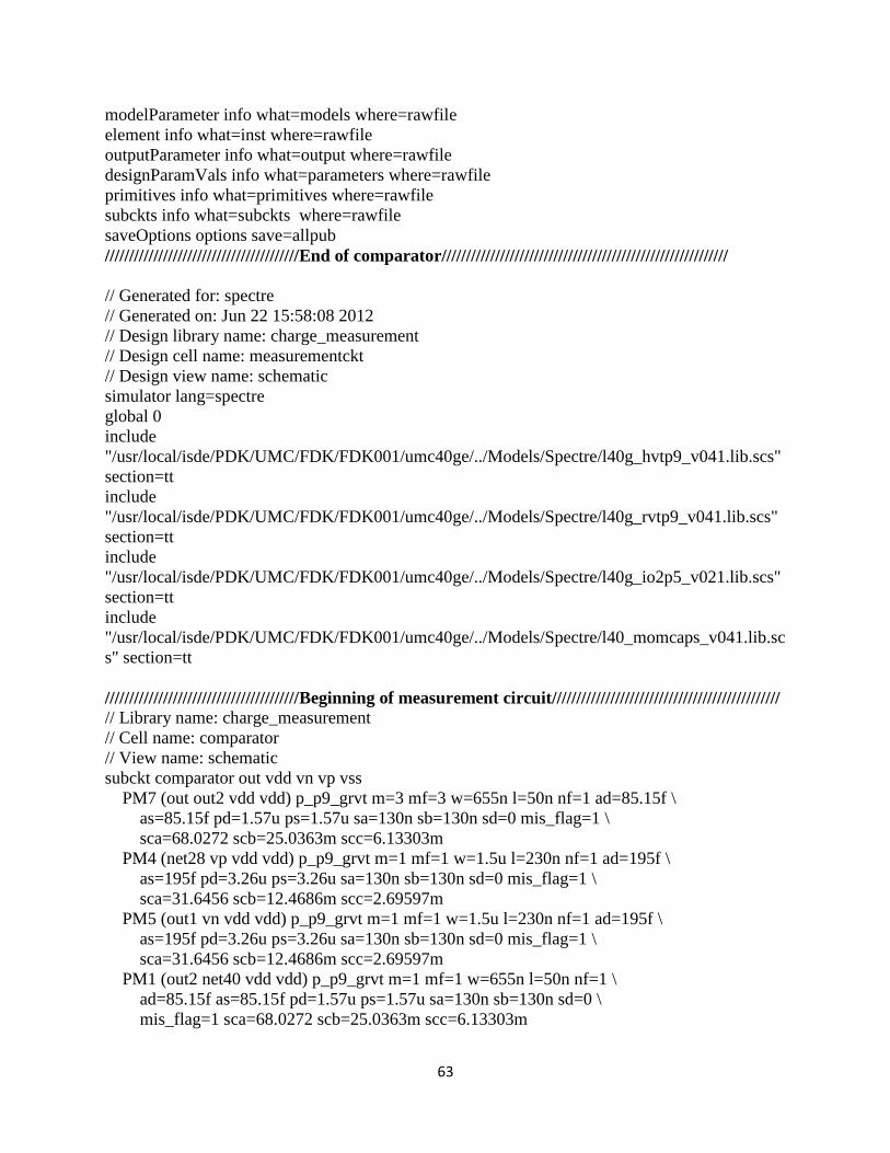
63
modelParameter info what=models where=rawfile
element info what=inst where=rawfile
outputParameter info what=output where=rawfile
designParamVals info what=parameters where=rawfile
primitives info what=primitives where=rawfile
subckts info what=subckts where=rawfile
saveOptions options save=allpub
////////////////////////////////////////End of comparator///////////////////////////////////////////////////////////
// Generated for: spectre
// Generated on: Jun 22 15:58:08 2012
// Design library name: charge_measurement
// Design cell name: measurementckt
// Design view name: schematic
simulator lang=spectre
global 0
include
"/usr/local/isde/PDK/UMC/FDK/FDK001/umc40ge/../Models/Spectre/l40g_hvtp9_v041.lib.scs"
section=tt
include
"/usr/local/isde/PDK/UMC/FDK/FDK001/umc40ge/../Models/Spectre/l40g_rvtp9_v041.lib.scs"
section=tt
include
"/usr/local/isde/PDK/UMC/FDK/FDK001/umc40ge/../Models/Spectre/l40g_io2p5_v021.lib.scs"
section=tt
include
"/usr/local/isde/PDK/UMC/FDK/FDK001/umc40ge/../Models/Spectre/l40_momcaps_v041.lib.sc
s" section=tt
////////////////////////////////////////Beginning of measurement circuit///////////////////////////////////////////////
// Library name: charge_measurement
// Cell name: comparator
// View name: schematic
subckt comparator out vdd vn vp vss
PM7 (out out2 vdd vdd) p_p9_grvt m=3 mf=3 w=655n l=50n nf=1 ad=85.15f \
as=85.15f pd=1.57u ps=1.57u sa=130n sb=130n sd=0 mis_flag=1 \
sca=68.0272 scb=25.0363m scc=6.13303m
PM4 (net28 vp vdd vdd) p_p9_grvt m=1 mf=1 w=1.5u l=230n nf=1 ad=195f \
as=195f pd=3.26u ps=3.26u sa=130n sb=130n sd=0 mis_flag=1 \
sca=31.6456 scb=12.4686m scc=2.69597m
PM5 (out1 vn vdd vdd) p_p9_grvt m=1 mf=1 w=1.5u l=230n nf=1 ad=195f \
as=195f pd=3.26u ps=3.26u sa=130n sb=130n sd=0 mis_flag=1 \
sca=31.6456 scb=12.4686m scc=2.69597m
PM1 (out2 net40 vdd vdd) p_p9_grvt m=1 mf=1 w=655n l=50n nf=1 \
ad=85.15f as=85.15f pd=1.57u ps=1.57u sa=130n sb=130n sd=0 \
mis_flag=1 sca=68.0272 scb=25.0363m scc=6.13303m
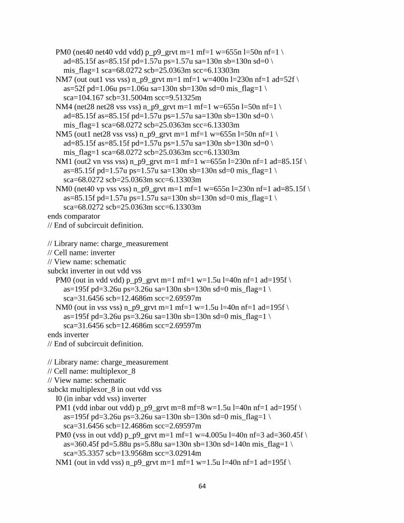
64
PM0 (net40 net40 vdd vdd) p_p9_grvt m=1 mf=1 w=655n l=50n nf=1 \
ad=85.15f as=85.15f pd=1.57u ps=1.57u sa=130n sb=130n sd=0 \
mis_flag=1 sca=68.0272 scb=25.0363m scc=6.13303m
NM7 (out out1 vss vss) n_p9_grvt m=1 mf=1 w=400n l=230n nf=1 ad=52f \
as=52f pd=1.06u ps=1.06u sa=130n sb=130n sd=0 mis_flag=1 \
sca=104.167 scb=31.5004m scc=9.51325m
NM4 (net28 net28 vss vss) n_p9_grvt m=1 mf=1 w=655n l=50n nf=1 \
ad=85.15f as=85.15f pd=1.57u ps=1.57u sa=130n sb=130n sd=0 \
mis_flag=1 sca=68.0272 scb=25.0363m scc=6.13303m
NM5 (out1 net28 vss vss) n_p9_grvt m=1 mf=1 w=655n l=50n nf=1 \
ad=85.15f as=85.15f pd=1.57u ps=1.57u sa=130n sb=130n sd=0 \
mis_flag=1 sca=68.0272 scb=25.0363m scc=6.13303m
NM1 (out2 vn vss vss) n_p9_grvt m=1 mf=1 w=655n l=230n nf=1 ad=85.15f \
as=85.15f pd=1.57u ps=1.57u sa=130n sb=130n sd=0 mis_flag=1 \
sca=68.0272 scb=25.0363m scc=6.13303m
NM0 (net40 vp vss vss) n_p9_grvt m=1 mf=1 w=655n l=230n nf=1 ad=85.15f \
as=85.15f pd=1.57u ps=1.57u sa=130n sb=130n sd=0 mis_flag=1 \
sca=68.0272 scb=25.0363m scc=6.13303m
ends comparator
// End of subcircuit definition.
// Library name: charge_measurement
// Cell name: inverter
// View name: schematic
subckt inverter in out vdd vss
PM0 (out in vdd vdd) p_p9_grvt m=1 mf=1 w=1.5u l=40n nf=1 ad=195f \
as=195f pd=3.26u ps=3.26u sa=130n sb=130n sd=0 mis_flag=1 \
sca=31.6456 scb=12.4686m scc=2.69597m
NM0 (out in vss vss) n_p9_grvt m=1 mf=1 w=1.5u l=40n nf=1 ad=195f \
as=195f pd=3.26u ps=3.26u sa=130n sb=130n sd=0 mis_flag=1 \
sca=31.6456 scb=12.4686m scc=2.69597m
ends inverter
// End of subcircuit definition.
// Library name: charge_measurement
// Cell name: multiplexor_8
// View name: schematic
subckt multiplexor_8 in out vdd vss
I0 (in inbar vdd vss) inverter
PM1 (vdd inbar out vdd) p_p9_grvt m=8 mf=8 w=1.5u l=40n nf=1 ad=195f \
as=195f pd=3.26u ps=3.26u sa=130n sb=130n sd=0 mis_flag=1 \
sca=31.6456 scb=12.4686m scc=2.69597m
PM0 (vss in out vdd) p_p9_grvt m=1 mf=1 w=4.005u l=40n nf=3 ad=360.45f \
as=360.45f pd=5.88u ps=5.88u sa=130n sb=130n sd=140n mis_flag=1 \
sca=35.3357 scb=13.9568m scc=3.02914m
NM1 (out in vdd vss) n_p9_grvt m=1 mf=1 w=1.5u l=40n nf=1 ad=195f \
65
as=195f pd=3.26u ps=3.26u sa=130n sb=130n sd=0 mis_flag=1 \
sca=31.6456 scb=12.4686m scc=2.69597m
NM0 (out inbar vss vss) n_p9_grvt m=8 mf=8 w=1.5u l=40n nf=1 ad=195f \
as=195f pd=3.26u ps=3.26u sa=130n sb=130n sd=0 mis_flag=1 \
sca=31.6456 scb=12.4686m scc=2.69597m
ends multiplexor_8
// End of subcircuit definition.
// Library name: charge_measurement
// Cell name: multiplexor_4
// View name: schematic
subckt multiplexor_4 in out vdd vss
I0 (in inbar vdd vss) inverter
PM1 (vdd inbar out vdd) p_p9_grvt m=4 mf=4 w=1.5u l=40n nf=1 ad=195f \
as=195f pd=3.26u ps=3.26u sa=130n sb=130n sd=0 mis_flag=1 \
sca=31.6456 scb=12.4686m scc=2.69597m
PM0 (vss in out vdd) p_p9_grvt m=1 mf=1 w=4.005u l=40n nf=3 ad=360.45f \
as=360.45f pd=5.88u ps=5.88u sa=130n sb=130n sd=140n mis_flag=1 \
sca=35.3357 scb=13.9568m scc=3.02914m
NM1 (out in vdd vss) n_p9_grvt m=1 mf=1 w=1.5u l=40n nf=1 ad=195f \
as=195f pd=3.26u ps=3.26u sa=130n sb=130n sd=0 mis_flag=1 \
sca=31.6456 scb=12.4686m scc=2.69597m
NM0 (out inbar vss vss) n_p9_grvt m=4 mf=4 w=1.5u l=40n nf=1 ad=195f \
as=195f pd=3.26u ps=3.26u sa=130n sb=130n sd=0 mis_flag=1 \
sca=31.6456 scb=12.4686m scc=2.69597m
ends multiplexor_4
// End of subcircuit definition.
// Library name: charge_measurement
// Cell name: multiplexor_2
// View name: schematic
subckt multiplexor_2 in out vdd vss
I0 (in inbar vdd vss) inverter
PM1 (vdd inbar out vdd) p_p9_grvt m=2 mf=2 w=1.5u l=40n nf=1 ad=195f \
as=195f pd=3.26u ps=3.26u sa=130n sb=130n sd=0 mis_flag=1 \
sca=31.6456 scb=12.4686m scc=2.69597m
PM0 (vss in out vdd) p_p9_grvt m=1 mf=1 w=4.005u l=40n nf=3 ad=360.45f \
as=360.45f pd=5.88u ps=5.88u sa=130n sb=130n sd=140n mis_flag=1 \
sca=35.3357 scb=13.9568m scc=3.02914m
NM1 (out in vdd vss) n_p9_grvt m=1 mf=1 w=1.5u l=40n nf=1 ad=195f \
as=195f pd=3.26u ps=3.26u sa=130n sb=130n sd=0 mis_flag=1 \
sca=31.6456 scb=12.4686m scc=2.69597m
NM0 (out inbar vss vss) n_p9_grvt m=2 mf=2 w=1.5u l=40n nf=1 ad=195f \
as=195f pd=3.26u ps=3.26u sa=130n sb=130n sd=0 mis_flag=1 \
sca=31.6456 scb=12.4686m scc=2.69597m
ends multiplexor_2
66
// End of subcircuit definition.
// Library name: charge_measurement
// Cell name: multiplexor
// View name: schematic
subckt multiplexor in out vdd vss
I0 (in inbar vdd vss) inverter
PM1 (vdd inbar out vdd) p_p9_grvt m=1 mf=1 w=1.5u l=40n nf=1 ad=195f \
as=195f pd=3.26u ps=3.26u sa=130n sb=130n sd=0 mis_flag=1 \
sca=31.6456 scb=12.4686m scc=2.69597m
PM0 (vss in out vdd) p_p9_grvt m=1 mf=1 w=4.005u l=40n nf=3 ad=360.45f \
as=360.45f pd=5.88u ps=5.88u sa=130n sb=130n sd=140n mis_flag=1 \
sca=35.3357 scb=13.9568m scc=3.02914m
NM1 (out in vdd vss) n_p9_grvt m=1 mf=1 w=1.5u l=40n nf=1 ad=195f \
as=195f pd=3.26u ps=3.26u sa=130n sb=130n sd=0 mis_flag=1 \
sca=31.6456 scb=12.4686m scc=2.69597m
NM0 (out inbar vss vss) n_p9_grvt m=1 mf=1 w=1.5u l=40n nf=1 ad=195f \
as=195f pd=3.26u ps=3.26u sa=130n sb=130n sd=0 mis_flag=1 \
sca=31.6456 scb=12.4686m scc=2.69597m
ends multiplexor
// End of subcircuit definition.
// Library name: charge_measurement
// Cell name: chargescalingDAC
// View name: schematic
subckt chargescalingDAC i0 i1 i2 i3 vdd vout vreset vss
V0 (vactual vss) vsource type=pwl wave=[ 2.25n 0 2.75n 56m 3.25n \
112.5m 3.75n 168m 4.25n 225m 4.75n 281.25m 5.25n 337.5m 5.75n \
393.75m 6.25n 450m 6.75n 506.25m 7.25n 562.5m 7.75n 618.75m 8.25n \
675m 8.75n 731.25m 9.25n 787.5m 9.75n 843.75m ]
I0 (i3 net29 vdd vss) multiplexor_8
I5 (i2 net25 vdd vss) multiplexor_4
I10 (i1 net17 vdd vss) multiplexor_2
C17 (vout net17 vss) momcaps_as_mmkf l=16.17u nf=13 nm=4 bm=1 m=2 \
mis_flag=1 metal_ring_flag=1 presim_flag=1
C18 (vout net25 vss) momcaps_as_mmkf l=16.17u nf=13 nm=4 bm=1 m=4 \
mis_flag=1 metal_ring_flag=1 presim_flag=1
C20 (vout net29 vss) momcaps_as_mmkf l=16.17u nf=13 nm=4 bm=1 m=8 \
mis_flag=1 metal_ring_flag=1 presim_flag=1
C1 (vout net21 vss) momcaps_as_mmkf l=16.17u nf=13 nm=4 bm=1 m=1 \
mis_flag=1 metal_ring_flag=1 presim_flag=1
C0 (vout vss) capacitor c=50f
NM0 (vout vreset vss vss) n_p9_grvt m=1 mf=1 w=1.5u l=40n nf=1 ad=195f \
as=195f pd=3.26u ps=3.26u sa=130n sb=130n sd=0 mis_flag=1 \
sca=31.6456 scb=12.4686m scc=2.69597m
I6 (i0 net21 vdd vss) multiplexor
67
ends chargescalingDAC
// End of subcircuit definition.
// Library name: charge_measurement
// Cell name: nand
// View name: schematic
subckt nand a b out vdd vss
PM1 (out b vdd vdd) p_p9_grvt m=1 mf=1 w=1.5u l=40n nf=1 ad=195f \
as=195f pd=3.26u ps=3.26u sa=130n sb=130n sd=0 mis_flag=1 \
sca=31.6456 scb=12.4686m scc=2.69597m
PM0 (out a vdd vdd) p_p9_grvt m=1 mf=1 w=1.5u l=40n nf=1 ad=195f \
as=195f pd=3.26u ps=3.26u sa=130n sb=130n sd=0 mis_flag=1 \
sca=31.6456 scb=12.4686m scc=2.69597m
NM1 (out a net14 vss) n_p9_grvt m=1 mf=1 w=1.5u l=40n nf=1 ad=195f \
as=195f pd=3.26u ps=3.26u sa=130n sb=130n sd=0 mis_flag=1 \
sca=31.6456 scb=12.4686m scc=2.69597m
NM0 (net14 b vss vss) n_p9_grvt m=1 mf=1 w=1.5u l=40n nf=1 ad=195f \
as=195f pd=3.26u ps=3.26u sa=130n sb=130n sd=0 mis_flag=1 \
sca=31.6456 scb=12.4686m scc=2.69597m
ends nand
// End of subcircuit definition.
// Library name: charge_measurement
// Cell name: nand3
// View name: schematic
subckt nand3 a b c out vdd vss
NM2 (net7 c vss vss) n_p9_grvt m=1 mf=1 w=1.5u l=40n nf=1 ad=195f \
as=195f pd=3.26u ps=3.26u sa=130n sb=130n sd=0 mis_flag=1 \
sca=31.6456 scb=12.4686m scc=2.69597m
NM1 (out a net15 vss) n_p9_grvt m=1 mf=1 w=1.5u l=40n nf=1 ad=195f \
as=195f pd=3.26u ps=3.26u sa=130n sb=130n sd=0 mis_flag=1 \
sca=31.6456 scb=12.4686m scc=2.69597m
NM0 (net15 b net7 vss) n_p9_grvt m=1 mf=1 w=1.5u l=40n nf=1 ad=195f \
as=195f pd=3.26u ps=3.26u sa=130n sb=130n sd=0 mis_flag=1 \
sca=31.6456 scb=12.4686m scc=2.69597m
PM2 (out a vdd vdd) p_p9_grvt m=1 mf=1 w=1.5u l=40n nf=1 ad=195f \
as=195f pd=3.26u ps=3.26u sa=130n sb=130n sd=0 mis_flag=1 \
sca=31.6456 scb=12.4686m scc=2.69597m
PM0 (out b vdd vdd) p_p9_grvt m=1 mf=1 w=1.5u l=40n nf=1 ad=195f \
as=195f pd=3.26u ps=3.26u sa=130n sb=130n sd=0 mis_flag=1 \
sca=31.6456 scb=12.4686m scc=2.69597m
PM1 (out c vdd vdd) p_p9_grvt m=1 mf=1 w=1.5u l=40n nf=1 ad=195f \
as=195f pd=3.26u ps=3.26u sa=130n sb=130n sd=0 mis_flag=1 \
sca=31.6456 scb=12.4686m scc=2.69597m
ends nand3
// End of subcircuit definition.
68
// Library name: charge_measurement
// Cell name: Tff_clear
// View name: schematic
subckt Tff_clear Q Q0 T clear clock vdd vss
I10 (clock clockb vdd vss) inverter
I8 (net24 Q0 Q vdd vss) nand
I7 (clockb net27 net19 vdd vss) nand
I6 (net40 clockb net24 vdd vss) nand
I4 (net53 net27 net40 vdd vss) nand
I9 (Q net19 clear Q0 vdd vss) nand3
I5 (net40 net47 clear net27 vdd vss) nand3
I3 (T clock Q net47 vdd vss) nand3
I2 (Q0 clock T net53 vdd vss) nand3
ends Tff_clear
// End of subcircuit definition.
// Library name: charge_measurement
// Cell name: 4bit_sync_counter
// View name: schematic
subckt charge_measurement_4bit_sync_counter_schematic clear_activelow \
clock enable_high out0 out1 out2 out3 vdd vss
I12 (net10 net11 vdd vss) inverter
I10 (net14 net45 vdd vss) inverter
I7 (net34 net19 vdd vss) inverter
I13 (out2 net45 net10 vdd vss) nand
I11 (out1 net19 net14 vdd vss) nand
I4 (enable_high out0 net34 vdd vss) nand
I3 (out3 net39 net11 clear_activelow clock vdd vss) Tff_clear
I2 (out2 net46 net45 clear_activelow clock vdd vss) Tff_clear
I1 (out1 net53 net19 clear_activelow clock vdd vss) Tff_clear
I0 (out0 net60 enable_high clear_activelow clock vdd vss) Tff_clear
ends charge_measurement_4bit_sync_counter_schematic
// End of subcircuit definition.
// Library name: charge_measurement
// Cell name: PeakDetector
// View name: schematic
subckt PeakDetector vdd vout vpeak vreset vss
PM2 (vout net0121 vdd vdd) p_p9_ghvt m=1 mf=1 w=1.5u l=40n nf=1 \
ad=195f as=195f pd=3.26u ps=3.26u sa=130n sb=130n sd=0 mis_flag=1 \
sca=31.6456 scb=12.4686m scc=2.69597m
PM3 (net0121 net0121 vdd vdd) p_p9_ghvt m=1 mf=1 w=1.5u l=40n nf=1 \
ad=195f as=195f pd=3.26u ps=3.26u sa=130n sb=130n sd=0 mis_flag=1 \
sca=31.6456 scb=12.4686m scc=2.69597m
NM2 (vout vreset vss vss) n_p9_ghvt m=1 mf=1 w=200n l=40n nf=1 ad=26f \
69
as=26f pd=660n ps=660n sa=130n sb=130n sd=0 mis_flag=1 sca=178.571 \
scb=34.6615m scc=14.4428m
C0 (vout vss vss) momcaps_sy_mmkf l=5u nf=10 nm=3 bm=1 m=9 mis_flag=1 \
metal_ring_flag=1 shielding_flag=0 presim_flag=1
NM0 (net13 vpeak vss vss) n_p9_grvt m=1 mf=1 w=655n l=230n nf=1 \
ad=85.15f as=85.15f pd=1.57u ps=1.57u sa=130n sb=130n sd=0 \
mis_flag=1 sca=68.0272 scb=25.0363m scc=6.13303m
NM1 (net17 vout vss vss) n_p9_grvt m=1 mf=1 w=655n l=230n nf=1 \
ad=85.15f as=85.15f pd=1.57u ps=1.57u sa=130n sb=130n sd=0 \
mis_flag=1 sca=68.0272 scb=25.0363m scc=6.13303m
NM5 (net21 net25 vss vss) n_p9_grvt m=1 mf=1 w=655n l=50n nf=1 \
ad=85.15f as=85.15f pd=1.57u ps=1.57u sa=130n sb=130n sd=0 \
mis_flag=1 sca=68.0272 scb=25.0363m scc=6.13303m
NM4 (net25 net25 vss vss) n_p9_grvt m=1 mf=1 w=655n l=50n nf=1 \
ad=85.15f as=85.15f pd=1.57u ps=1.57u sa=130n sb=130n sd=0 \
mis_flag=1 sca=68.0272 scb=25.0363m scc=6.13303m
NM6 (net0121 net21 vss vss) n_p9_grvt m=1 mf=1 w=400n l=230n nf=1 \
ad=52f as=52f pd=1.06u ps=1.06u sa=130n sb=130n sd=0 mis_flag=1 \
sca=104.167 scb=31.5004m scc=9.51325m
PM0 (net13 net13 vdd vdd) p_p9_grvt m=1 mf=1 w=655n l=50n nf=1 \
ad=85.15f as=85.15f pd=1.57u ps=1.57u sa=130n sb=130n sd=0 \
mis_flag=1 sca=68.0272 scb=25.0363m scc=6.13303m
PM1 (net17 net13 vdd vdd) p_p9_grvt m=1 mf=1 w=655n l=50n nf=1 \
ad=85.15f as=85.15f pd=1.57u ps=1.57u sa=130n sb=130n sd=0 \
mis_flag=1 sca=68.0272 scb=25.0363m scc=6.13303m
PM5 (net21 vout vdd vdd) p_p9_grvt m=1 mf=1 w=1u l=230n nf=1 ad=130f \
as=130f pd=2.26u ps=2.26u sa=130n sb=130n sd=0 mis_flag=1 \
sca=46.2963 scb=18.1908m scc=4.04276m
PM4 (net25 vpeak vdd vdd) p_p9_grvt m=1 mf=1 w=1u l=230n nf=1 ad=130f \
as=130f pd=2.26u ps=2.26u sa=130n sb=130n sd=0 mis_flag=1 \
sca=46.2963 scb=18.1908m scc=4.04276m
PM6 (net0121 net17 vdd vdd) p_p9_grvt m=3 mf=3 w=655n l=50n nf=1 \
ad=85.15f as=85.15f pd=1.57u ps=1.57u sa=130n sb=130n sd=0 \
mis_flag=1 sca=68.0272 scb=25.0363m scc=6.13303m
ends PeakDetector
// End of subcircuit definition.
// Library name: charge_measurement
// Cell name: measurementckt
// View name: schematic
I7 (_3 vdd DAC_out PD_out vss) comparator
I5 (_3 _2 vdd vss) inverter
C0 (node vss vss) momcaps_sy_mmkf l=5u nf=10 nm=3 bm=1 m=9 mis_flag=1 \
metal_ring_flag=1 shielding_flag=0 presim_flag=1
PM0 (node vdd vdd vdd) p_2p5_g m=1 mf=1 w=1u l=270n nf=1 sa=170n sb=170n \
sd=0 mis_flag=1 ad=170f as=170f pd=2.34u ps=2.34u sca=14.9031 \
70
scb=13.6621m scc=1.77252m
I4 (vddhit node) isource type=pwl wave=[ 3n 0 3.05n 150u 3.21n 50u 3.4n \
50u 5.4n 0 ]
NM0 (node vreset vss vss) n_p9_grvt m=1 mf=1 w=2u l=40n nf=1 ad=260f \
as=260f pd=4.26u ps=4.26u sa=130n sb=130n sd=0 mis_flag=1 \
sca=24.0385 scb=9.38101m scc=2.02198m
I2 (o0 o1 o2 o3 vdd DAC_out vreset vss) chargescalingDAC
I1 (clear clock _2 o0 o1 o2 o3 vdd vss) \
charge_measurement_4bit_sync_counter_schematic
I0 (vdd PD_out node vreset vss) PeakDetector
include "./_graphical_stimuli.scs"
simulatorOptions options reltol=1e-3 vabstol=1e-6 iabstol=1e-12 temp=27 \
tnom=25 scalem=1.0 scale=1.0 gmin=1e-12 rforce=1 maxnotes=5 maxwarns=5 \
digits=5 cols=80 pivrel=1e-3 sensfile="../psf/sens.output" \
checklimitdest=psf
tran tran stop=16n write="spectre.ic" writefinal="spectre.fc" \
annotate=status maxiters=5
finalTimeOP info what=oppoint where=rawfile
modelParameter info what=models where=rawfile
element info what=inst where=rawfile
outputParameter info what=output where=rawfile
designParamVals info what=parameters where=rawfile
primitives info what=primitives where=rawfile
subckts info what=subckts where=rawfile
save I4:sink
saveOptions options save=allpub
////////////////////////////////////////End of measurement circuit/////////////////////////////////////////////////////////