Embed Size (px)
Citation preview
This document is downloaded from DR‑NTU (https://dr.ntu.edu.sg)Nanyang Technological University, Singapore.
Characterization, design and modeling of on‑chipinterleaved transformers
Zhao, Dan
2008
Zhao, D. (2008). Characterization, design and modeling of on‑chip interleavedtransformers. Master’s thesis, Nanyang Technological University, Singapore.
https://hdl.handle.net/10356/14507
https://doi.org/10.32657/10356/14507
Downloaded on 30 Dec 2021 00:37:57 SGT

Characterization, Design and Modeling of On-Chip Interleaved Transformers
ZHAO DAN
School of Electrical & Electronic Engineering
A thesis submitted to the Nanyang Technological University
in partial fulfillment of the requirement for the degree of Master of Engineering
2008
ATTENTION: The Singapore Copyright Act applies to the use of this document. Nanyang Technological University Library

i
Acknowledgement
First and foremost, I would like to extend my appreciation to my supervisor in Nanyang Technological
University (NTU), Assoc. Prof. Yeo Kiat Seng, for giving me this opportunity to undertake this project
and learn valuable skills and knowledge through this project. I would also like to thank him for his
patience, encouragement, and advice for guiding me throughout the project.
I wish to extend special thanks to Mr. Andy Wong from Advanced RFIC (Singapore) Pte Ltd for
accepting me as a master student in the Joint Industry Postgraduate (JIP) program. He also provided me
continuous support and valuable comments.
Besides, I am very grateful to Mr. Lim Chee Chong, a PhD student in NTU, for his help with the software
that I have used extensively in this project and his valuable advice on the layout and modeling. I am also
grateful to Mr. Lim Wei Meng, a research associate of NTU, for his help in providing me measurement
data and advice.
Last but not least, I wish to extend special thanks to the technical staff in NTU, School of EEE, IC Design
1 laboratory, Ms. Chan Nai Hong, Corrie, for her countless help given to me.
ATTENTION: The Singapore Copyright Act applies to the use of this document. Nanyang Technological University Library

ii
Abstract
This report aims to provide a comprehensive review of the project, characterization, design and modeling
of on-chip interleaved transformers. Investigation, modeling, and performance optimization of silicon-
based on-chip transformers are deliberately addressed.
Complete characterization of monolithic planar interleaved transformers was performed based on 3D EM
(Electromagnetic) simulations. The effect of layout geometry on the transformer’s performance was
investigated. The number of turns of the octagonal spiral, the inner radius of the spiral, the metal line
width, and the metal spacing were each varied independently, while the other parameters were kept
unchanged. The conclusion of the report could serve as useful design guidelines.
Various loss mechanisms that degrade the transformer’s performance were examined. A scalable model
has been proposed to represent the RF characteristics of different transformer designs. All the RLC model
elements were formulated as functions of the transformer’s geometrical and process parameters. Thus, the
flexibility to tailor the transformer design becomes possible for any RF applications. Verification with
accurately calibrated EM simulations demonstrated the accuracy of the performance predication and the
scalability for a wide range of transformers’ layout.
A 5GHz Gilbert Cell mixer was finally designed to test the capability of the proposed transformer. The
transformer works as an input balun to generate differential signals. Resonant tuning was added to reduce
the losses between input and output ports. The designed mixer offers high conversion gain, excellent
isolations, as well as good linearity and noise performances.
ATTENTION: The Singapore Copyright Act applies to the use of this document. Nanyang Technological University Library

iii
List of Symbols
N Number of turns
IR Inner radius
W Metal width
S Turn-to-turn spacing
t Metal layer thickness
teff Effective thickness of the conductor
LGML Geometric mean length of the circular inductor
P Metal trace pitch
�r Relative permittivity, �Al-Cu = 1, �Si = 11.8
�0 Absolute permeability
�r Relative permeability, �Al-Cu = 0.9991
�0 Absolute permeability
f Frequency
w Angular frequency
CuAl−ρ Resistivity of the metal layer, mCuAl ⋅Ω−×=−710
1.4
1ρ
Siρ Resistivity of the silicon substrate
c Speed of light
CSUB Substrate capacitance (per unit area)
GSUB Substrate conductance (per unit area)
ATTENTION: The Singapore Copyright Act applies to the use of this document. Nanyang Technological University Library
iv
List of Figures
Figure 2.1 On-chip transformer layouts (top view): (a) Tapped, (b) interleaved, (c) stacked with top spiral
overlapping the bottom one, and (d) side view of stacked spirals [9] ........................................................... 6
Figure 2.2 Formation of substrate eddy currents [21] ................................................................................. 10
Figure 2.3 Equivalent circuit model for planar interleaved transformers [10] ............................................ 11
Figure 2.4 The lumped-equivalent-circuit of the transformer [11] ............................................................. 12
Figure 2.5 A two-coil on-chip differential transformer [25] ....................................................................... 13
Figure 2.6 Parallel-plate capacitance and fringing capacitance .................................................................. 17
Figure 3.1 Layout of a four-port interleaved transformer with a turn ratio n = 3:3 .................................... 20
Figure 3.2 The transformer with different port configurations: (a) four-port, (b) three-port, ..................... 21
Figure 3.3 An example of HFSS set-up for a 7-turn inductor ..................................................................... 23
Figure 3.4 Planar view of the HFSS set-up for a 7-turn inductor ............................................................... 25
Figure 3.5 Comparisons of simulation results obtained from different HFSS set-up ................................. 25
Figure 3.6 Comparisons of simulated and measured (a) L and Q of the primary coil, (b) two-port S21, and
(c) four-port S21 for a 4-turn transformer ................................................................................................... 28
Figure 3.7 (a) Magnetic field, and (b) current density along the conductor for the transformer with N = 3,
IR = 50 um, W = 5 um, S = 2 um ................................................................................................................. 30
Figure 3.8 (a) Magnetic field, and (b) Current density in the substrate for the transformer with N = 3, IR =
50 um, W = 5 um, S = 2 um ......................................................................................................................... 31
Figure 3.9 Simplified model for transformers at lower frequencies ........................................................... 32
Figure 4.1 (a) Qp and (b) Lp versus frequency for varying number of turns ............................................... 35
Figure 4.2 Positive and negative mutual inductance components in the primary coil [24] ........................ 36
Figure 4.3 K versus frequency for varying N .............................................................................................. 37
Figure 4.4 Gmax versus frequency for varying N ......................................................................................... 37
Figure 4.5 (a) Lp, and (b) Qp versus frequency for varying IR .................................................................... 39
Figure 4.6 (a) Gmax and (b) K versus frequency for varying IR ................................................................... 41
ATTENTION: The Singapore Copyright Act applies to the use of this document. Nanyang Technological University Library

v
Figure 4.5 (a) Lp, and (b) Qp versus frequency for varying IR .................................................................... 39
Figure 4.6 (a) Gmax and (b) K versus frequency for varying IR ................................................................... 41
Figure 4.7 (a) Lp, and (b) Qp versus frequency for varying W .................................................................... 43
Figure 4.8 (a) Gmax, and (b) K versus frequency for varying W .................................................................. 44
Figure 4.9 K versus frequency for varying S .............................................................................................. 45
Figure 4.10 Qp versus frequency for varying S ........................................................................................... 45
Figure 4.11 The design flowchart ............................................................................................................... 48
Figure 4.12 Contour plots of Q versus varying IR and W at (a) 0.6 GHz, (b) 1.6 GHz and (c) 3.0 GHz .... 49
Figure 5.1 2-� model of the primary winding ............................................................................................ 51
Figure 5.2 Lumped-element equivalent-circuit model for on-chip interleaved transformer ....................... 52
Figure 5.3 Parasitic capacitances in the transformer ................................................................................... 61
Figure 5.4 Comparisons of simulated and model results: (a) two-port S11, S21, S22, (b) four-port S11,
S21, S22, and (c) Lp and Qp (N = 3, IR = 50 um, W = 6 um and S = 2 um) ................................................. 70
Figure 5.5 Comparisons of simulated and model results: (a) two-port S11, S21, S22, and (b) Lp and Qp (N
= 2, IR = 50 um, W = 12 um and S = 2 um) ................................................................................................. 72
Figure 5.6 Comparisons of simulated and model results: (a) two-port S11, S21, S22, and (b) Lp and Qp (N
= 3, IR = 100 um, W = 12 um and S = 2 um) ............................................................................................... 74
Figure 6.1 Folding of RF and image noise into the IF band [49] ................................................................ 76
Figure 6.2 |S21| (dB) versus frequency for varying IR ............................................................................... 79
Figure 6.3 Comparison of inverting and non-inverting S21 of a 3-turn transformer .................................. 79
Figure 6.4 Gilbert cell mixer topology ....................................................................................................... 80
Figure 6.5 Conversion Gain vs RF frequency ............................................................................................. 81
Figure 6.6 Mixer two tone test .................................................................................................................... 82
Figure 6.7 Isolations of LO to RF and RF to IF vs RF frequency .............................................................. 82
Figure 6.8 SSB Noise Figure vs RF frequency ........................................................................................... 82
Figure 6.9 Core layout of the transformer-based mixer including the transformer ..................................... 83
ATTENTION: The Singapore Copyright Act applies to the use of this document. Nanyang Technological University Library
List of Tables
Table 1 Comparison of transformer layouts [9] …………………………………………………………………….. 7
Table 2 Technological Parameters ………………………………………………………………………………….. 23
Table 3 Comparison of measured and simulated results of inductors ……………………………. 26
Table 4 Transformer Performance Parameters Extraction ……………………………………....... 33
Table 5 Interleaved Transformer Performance Trends ………………………………………………… 46
Table 6 Analytical Formula for Circuit Elements ………………………………………………………………… 58
Table 7 Geometrical and circuit parameters of transformer model …………………………….. 64
Table 8 Value of RLC elements in the circuit model …………………………………………………….. 65
Table 9 Mixer summary ……………………………………………………………………………………………………….. 84
ATTENTION: The Singapore Copyright Act applies to the use of this document. Nanyang Technological University Library

vii
Table of Contents
Acknowledgement ........................................................................................................................................ i
Abstract ....................................................................................................................................................... ii
List of Symbols ........................................................................................................................................... iii
List of Figures ............................................................................................................................................ iv
List of Tables .............................................................................................................................................. vi
Chapter 1 Introduction .............................................................................................................................. 1
1.1 Background 1
1.2 Objectives 3
1.3 Organization of the Report 3
Chapter 2 Literature Review ..................................................................................................................... 5
2.1 Layouts of On-Chip Transformers 5
2.2 Loss Mechanisms in Si-based Transformers 7
2.2.1 Series resistance 8
2.2.2 Substrate capacitive and resistive losses 9
2.2.3 Substrate magnetic losses 10
2.3 Transformer Models 11
2.3.1 DC inductance calculation 14
2.3.2 Skin and proximity effects 14
2.3.3 Substrate network 16
2.3.4 Parasitic capacitance 17
Chapter 3 Transformer Layout ............................................................................................................... 19
3.1 Transformer Structure 19
3.2 HFSS (High Frequency Structure Simulator) Simulation 21
ATTENTION: The Singapore Copyright Act applies to the use of this document. Nanyang Technological University Library

viii
3.2.1 Calibration of HFSS 22
3.3 Transformer Performance Parameters Extraction 31
Chapter 4 Characterization of On-Chip Transformers ........................................................................ 34
4.1 Effects of the Transformer’s Physical Dimensions 34
4.1.1 Number of turns (N) 34
4.1.2 Inner radius (IR) 38
4.1.3 Metal line width (W) 41
4.1.4 Turn-to-turn spacing (S) 44
4.2 Design Methodology 46
Chapter 5 Modeling .................................................................................................................................. 50
5.1 Generation of Transformer Model 50
5.2 Analytical RLC Element Calculations 53
5.2.1 Inductance calculation 53
5.2.2 Ladder circuit elements calculation [14] 54
5.2.3 Substrate network 59
5.2.4 Parasitic capacitances 61
5.2.5 K-factor 63
5.3 Model Verification 64
Chapter 6 A 5 GHz Gilbert Cell Mixer with Transformer-Balun ........................................................ 75
6.1 General Considerations 75
6.2 Transformer Design 77
6.3 Circuit Design 80
Chapter 7 Conclusions and Recommendations ...................................................................................... 85
7.1 Conclusions 85
7.2 Recommendations 87
References .................................................................................................................................................. 88
Author’s Publications ............................................................................................................................... 95
ATTENTION: The Singapore Copyright Act applies to the use of this document. Nanyang Technological University Library

ix
Appendix 1 A VB Script to Generate Transformer Structure in HFSS .............................................. 96
Appendix 2 Geometrical Mean Length (LGML) Calculation .................................................................100
ATTENTION: The Singapore Copyright Act applies to the use of this document. Nanyang Technological University Library
Chapter 1 Introduction
1
Chapter 1 Introduction
1.1 Background
Driven by the recent rapid growth of wireless communication and mobile applications, there is an
insatiable demand for low-cost integrated radio systems in silicon technology. Traditionally, radio systems
are implemented using a large number of discrete components. Speedy improvements in modern CMOS
technologies, for example, low fabrication cost and high packing density, make it possible to realize RF
circuits also in CMOS [1, 2].
The advantages of integrating radio frequency (RF) circuits are compelling. The fewer the external
components, the smaller the size of the circuit board and perhaps the smaller the power consumption.
These two advantages are especially significant in the rapidly expanding personal communication services
market, where portability and long battery life are essential. Furthermore, it minimizes the number of
external connections that require soldering. Thereby, the reliability and robustness of the end product
could be enhanced. Component matching could be done at an easier design stage as well [3]. Thus, more
flexibility to choose high performance architectures could be offered. Finally, as the level of integration
increases, two key issues i.e., testing time and cost, are reduced in the communications area, where time to
market is paramount.
The demand for high performance radio frequency integrated circuits (RFICs) on silicon has generated
increasing interest in on-chip passive components (inductors and transformers). Transformers are
important elements in RF designs for impedance transformation and matching, balun implementation,
bandwidth enhancement, etc. Specific applications include low-loss feedback and single-ended-to-
differential signal conversion in a 1.9 GHz receiver front end [4], and matching and coupling in an image
ATTENTION: The Singapore Copyright Act applies to the use of this document. Nanyang Technological University Library

Chapter 1 Introduction
2
rejection mixer [5] and in balanced amplifiers [6-8]. Hence, there is a great incentive to design, optimize,
and model RF transformers fabricated on Si substrates.
However, monolithic integrated transformers have parasitic effects and imperfect coupling between the
windings. They stem from the complexity of high-frequency phenomena such as the eddy current and
substrate losses in the silicon. It is a prerequisite for a successful design with integrated transformers to
employ sufficient specification including at least the main electrical parameters, such as the inductance,
coupling factor of the windings, ohmic loss in the conductor, parasitic capacitive coupling between the
windings, parasitic coupling into the substrate and finally substrate loss. Although on-chip transformers
have been employed in RFICs, up to now, there is no systematic way to model and predict the electrical
characteristic of on-chip transformers.
In order to exploit the capabilities offered by a monolithic transformer, limitations imposed by silicon
technology upon the component performance must be accurately modeled and characterized. One solution
is to use field solvers such as Ansoft’s High-Frequency Structure Simulator (HFSS)TM or Momentum in
Advanced Design System (ADS) TM. These tools, through careful calibration, can provide accurate
simulation results. Designers have the option to change any parameter in the design to optimize the
performance or to perform the parameter sensitivity analysis. However, they can only give the port
behaviors of the device, such as the S-parameters in a tabular format. They do not provide any insight into
the engineering trade-offs involved in the transformer design. The other solution is to create the equivalent
circuit model of the transformer, using lumped RLC elements [9-12]. The use of lumped-element
approximation is valid because the physical length of each conducting segment is much smaller than the
guided wavelength λ [13]. Such models can be easily incorporated into a standard circuit design
environment, such as the SPICE circuit simulator. Several benefits are thus naturally guaranteed. Firstly,
both frequency and time domain can be covered and the ability to perform noise analysis is ensured.
Secondly, most of the parasitic capacitances and resistances in theses models have simple, physically
intuitive and analytical expressions. Generally, models of higher order complexity give better accuracy.
ATTENTION: The Singapore Copyright Act applies to the use of this document. Nanyang Technological University Library
Chapter 1 Introduction
3
In this project, the 3-dimensional electromagnetic (3D EM) simulation, Ansoft’s High-Frequency
Structure Simulator (HFSS)TM [14], was used to characterize the planar interleaved transformer. The effect
of layout geometry upon the transformer performance was investigated. The factors limiting the
transformer’s performance were identified. Also a lumped equivalent-circuit model used for describing the
electronic behavior of the transformer was developed, which is scalable over a wide range of layout
dimensions. The model gives accurate predication of the electrical behavior with low complexity.
1.2 Objectives
The objectives of this project are summarized as follows:
1. To study and understand the various loss mechanisms that degrade the performance of
silicon-based on-chip interleaved transformers.
2. To characterize the transformer by studying the effect of physical dimensions on the
transformer’s performance.
3. To find a design guide on how to design close-to-optimal transformers.
4. To develop an accurate but simple lumped element model for the transformer based on the
calibrated simulation data.
5. To test the capability of the proposed transformer in a 5GHz Gilbert cell mixer.
1.3 Organization of the Report
There are totally 7 chapters in this report. Chapter 1 gives an overview of this project by presenting the
motivation and objectives.
ATTENTION: The Singapore Copyright Act applies to the use of this document. Nanyang Technological University Library
Chapter 1 Introduction
4
Chapter 2 reviews the work done by other researchers. Transformers with different layouts are discussed.
Also various loss mechanisms pertaining to transformers are introduced. Besides, the available interleaved
transformer’s models are presented.
Chapter 3 gives a brief introduction of Ansoft HFSS and the interleaved transformer structure. Also the
simulation results obtained from HFSS are carefully calibrated to verify the transformer structure and its
accuracy in predicting the transformer’s behaviors.
Chapter 4 focuses on the characterization of the transformer. The number of turns (N), inner radius (IR),
track width (W), turn-to-turn spacing (S), and metal thickness (t) of the transformer are varied
independently to study the resultant changes on the transformer’s performance, such as the quality factor
Q, self-inductance L, the coupling factor K, the maximum available gain Gmax and the resonant frequency
fres. This chapter also includes a detailed design methodology of the interleaved transformer and how its
geometrical parameters are determined.
Chapter 5 concentrates on the modeling of interleaved transformers. A lumped equivalent-circuit model is
developed, which is scalable over a wide range of layout dimensions (N, IR, W, and S). A set of analytical
formula are developed to calculate the value of each RLC element in the model. Verification with
simulation data demonstrates accurate performance predication and good scalability for a wide range of
transformer layout.
Chapter 6 introduces a 5GHz Gilbert Cell mixer designed to test the capability of the transformer
designed. The transformer worked as an input balun to generate differential signals. Resonant tuning was
added to reduce the losses between input and output ports. The designed mixer could provide high
conversion gain, good linearity and noise performances, and excellent isolations.
Finally, Chapter 7 summarizes this work and proposes a few key areas for future research.
ATTENTION: The Singapore Copyright Act applies to the use of this document. Nanyang Technological University Library

Chapter 2 Literature Review
5
Chapter 2 Literature Review
2.1 Layouts of On-Chip Transformers
Similar to on-chip spiral inductors, on-chip transformers can also be designed in various geometries.
Monolithic planar transformers based on different layouts, have been studies in the past few years [9-13,
15-17].
The desired characteristics of a transformer are application dependent. Transformers can be configured as
three- or four-terminal devices. They may be used for narrowband or broadband applications. For
example, in single ended to differential conversion, the transformer might be used as a four-terminal
narrowband device. In this case, a high mutual coupling coefficient and high self-inductance are desired
along with low series resistance. On the other hand, for bandwidth extension applications, the transformer
is used as a broadband three-terminal device. Therefore, a small mutual coupling coefficient and high
series resistance are acceptable while all capacitances need to be minimized [9, 18].
The tapped transformer (Figure 2.1 (a)) is best suited for three-port applications. It permits a variety of
tapping ratios to be realized. This transformer relies only on lateral magnetic coupling. All windings can
be implemented with the top metal layer, thereby minimizing port-to-substrate capacitances. Since the two
inductors occupy separate regions, the self-inductance is maximized while the port-to-port capacitance is
minimized. Unfortunately, this spatial separation also leads to low mutual coupling ( 5.0~3.0≈K ).
The interleaved transformer (Figure 2.1 (b)) is best suited for four-port applications that demand
symmetry. Once again, capacitances can be minimized by implementation on top level metal so that high
resonant frequencies may be realized. The interleaving of the two inductances permits moderate coupling
ATTENTION: The Singapore Copyright Act applies to the use of this document. Nanyang Technological University Library

Chapter 2 Literature Review
6
( 7.0≈K ) to be achieved at the cost of reduced self-inductance. This coupling may be increased at the
cost of higher series resistance by reducing the turn width (W) and spacing (S).
(a) (b)
(c) (d)
Figure 2.1 On-chip transformer layouts (top view): (a) Tapped, (b) interleaved, (c) stacked with top spiral
overlapping the bottom one, and (d) side view of stacked spirals [9]
The stacked transformer (Figure 2.1 (c)) uses multiple metal layers and exploits both vertical and lateral
magnetic coupling to provide the best area efficiency, the highest self-inductance and the highest coupling
( 9.0≈K ). This configuration is suitable for both three- and four-terminal configurations. The main
drawback is the high port-to-port capacitance, or equivalently a low self-resonance frequency. In some
cases, such as narrowband impedance transformers, this capacitance may be incorporated as part of the
resonant circuit. However, in modern multi-level processes, the capacitance can be reduced by increasing
the oxide thickness between spirals. For example, in a five metal process, reductions in port-to-port
Inner Spiral
Outer Spiral
Primary Secondary
Side View S=2um
Bottom Spiral
ATTENTION: The Singapore Copyright Act applies to the use of this document. Nanyang Technological University Library

Chapter 2 Literature Review
7
capacitance can be achieved by implementing the spirals on layers five and three instead of five and four.
The increased vertical separation will reduce K by less than 5% [9].
Table 1 summarizes the performance of the above mentioned three configurations. Various trade-offs of
different configurations are offered among the self-inductance and series resistance of each port, the
mutual coupling factor, the port-to-port and port-to-substrate capacitances, resonance frequencies,
symmetry and area efficiency. Therefore, additional layouts have been presented by researchers to make a
compromise between different configurations. The structure we used in this project is a center-tapped
interleaved transformer, which is physically symmetrical and can provide a compromise between the
tapped and interleaved transformers (see Chapter 3).
Table 1 Comparison of transformer layouts [9]
Type Area Coupling factor, K Self-inductance Self-resonant frequency
Tapped High Low Mid High
Interleaved High Mid Low High
Stacked Low High High Low
2.2 Loss Mechanisms in Si-based Transformers
In general, there are four main loss mechanisms associated with a Si-based on-chip transformer. They are
metallization resistive loss, substrate capacitive, resistive and magnetic losses, respectively.
ATTENTION: The Singapore Copyright Act applies to the use of this document. Nanyang Technological University Library

Chapter 2 Literature Review
8
2.2.1 Series resistance
For a single metal line, the dc current is uniformly distributed inside the conductor. However, as frequency
goes up, the current density becomes nonuniform due to the induced electromotive force (EMF) and the
formation of eddy currents. The eddy current effect occurs when a conductor is subjected to time-varying
magnetic fields. Eddy currents manifest themselves as skin and proximity effects.
In the case of the skin effect, the time-varying magnetic field due to the current flow in a conductor
induces eddy currents in the conductor itself. Eddy currents produce their own magnetic fields to oppose
the original field, thus reducing the net magnetic flux and causing a decrease in current flow as depth
increases. In other words, the depth of current penetrating into the metal (skin depth) becomes compatible
to or even smaller than the cross-sectional dimensions of the wire, which means there will be an increase
in the series resistance.
The proximity effect takes place when a conductor is under the influence of a time-varying field produced
by a nearby conductor carrying a time-varying current. It has a greater impact than the skin effect on the
increase of resistance and degradation of Q in present-day spiral inductor/transformer designs. Moreover,
in this case, eddy currents are induced whether or not the first conductor carries current. This is essentially
a transformer action. If the first conductor does carry a time-varying current, then the skin-effect eddy
current and the proximity-effect eddy current superimpose to form the total eddy current distribution.
Regardless of the induction mechanism, eddy currents reduce the net current flow in the conductor and
hence increase the ac resistance. The distribution of eddy currents depends on the geometry of the
conductor and its orientation with respect to the impinging time-varying magnetic field [19]. And the
severity of the eddy current effect is determined by the ratio of skin depth to the conductor thickness. The
eddy current effect is negligible only if the depth of penetration is much greater than the conductor
ATTENTION: The Singapore Copyright Act applies to the use of this document. Nanyang Technological University Library

Chapter 2 Literature Review
9
thickness. The most critical parameter pertaining to eddy current effects is the skin depth, which is defined
as
fπμρδ = (4.1)
where μ , ρ , and f represent the resistivity in �-m, permeability in H/m, and frequency in Hz,
respectively.
2.2.2 Substrate capacitive and resistive losses
Due to the relatively low resistivity of silicon (typically within the range of 0.01 �-cm to 15 �-cm
depends on process technology), substrate losses are the most important factor degrading the performance
of Si-based integrated transformers.
In a CMOS process, the windings of the spiral are separated from the substrate by a thin layer of silicon
dioxide (SiO2). This creates capacitance (Cox) between the spiral and the surface of the substrate. Besides,
the silicon substrate has a relative permittivity of around 11.8 for typical CMOS/BiCMOS processes and
is tied ground potential in most CMOS processes, forming substrate capacitance (Csub). This substrate
capacitance has two detrimental effects on a monolithic transformer: 1) it allows RF currents to interact
with the substrate, lowering the inductance and quality factor; and 2) it increases parasitic capacitances,
reducing the resonant frequency. Reducing the trace width can decrease this capacitance, but at the
expense of increasing the series resistance of the inductor. This is an important tradeoff since wide traces
are generally used in transformers on silicon to overcome the low thin-film conductivity of the
metallization. This also limits the feasibility of creating arbitrarily large valued inductances [20].
ATTENTION: The Singapore Copyright Act applies to the use of this document. Nanyang Technological University Library

Chapter 2 Literature Review
10
The parasitic resistance, on the other hand, refers to the resistance of the silicon substrate (Rsub) owing to
finite resistance of substrate. Process related methods, such as increasing substrate resistivity, removing
silicon substrate underneath, and increasing dielectric thickness, etc, can minimize the parasitic effects.
2.2.3 Substrate magnetic losses
There are also losses due to the magnetic field in the transformer structure. The magnetic field extends
around the windings of the spiral and into the substrate. Faraday’s Law states that this time-varying
magnetic field induces an electric field in the substrate. This field forces an image current (eddy current)
to flow in the substrate in the opposite direction of the current in the winding directly above it. Since the
silicon substrate has low resistivity, the image current can flow easily and this leads to undesirable power
dissipation [21].
Figure 2.2 Formation of substrate eddy currents [21]
Figure 2.2 illustrates how magnetic field is generated by the inductor current, to penetrate into the
conductive substrate and eventually induce eddy current. The induced current, which is opposite to that of
the winding, generates an opposing parasitic magnetic field in the substrate. This parasitic magnetic field
Via
Field oxide
Substrate
Current flowing into paper
Spiral Windings
Underpass
Substrate Magnetic Field
Magnetic Field
Current flowing out of paper
ATTENTION: The Singapore Copyright Act applies to the use of this document. Nanyang Technological University Library

Chapter 2 Literature Review
11
interacts with the magnetic field and results in a degradation of the inductance. Also, power dissipated due
to eddy current flows degrades the value of Q. Moreover, as the substrate magnetic loss is frequency
dependent, the eddy current increases with rising frequency. This effect can also be thought of as a
parasitic transformer, where the substrate represents an unwanted secondary winding. Larger inductors
have magnetic fields that penetrate deeper into the substrate, hence suffer from higher substrate losses.
This effect is in opposition to the goal of limiting series resistance with wide spiral traces [20]. Use of
nonstandard high-resistivity silicon substrates [22], or a post-process micromachining step to etch the
substrate away under the inductor [23], can minimize these substrate effects.
2.3 Transformer Models
As mentioned, the behavior of monolithic transformer is layout sensitive. Different models should be used
to model transformers with different configurations. In [9], two distinct models were proposed for tapped
and stacked transformers. Component values in these models are derived from transformer’s geometrical
and process parameters.
Figure 2.3 Equivalent circuit model for planar interleaved transformers [10]
C1,2
L1 L2
R1 R2
Port 2 Port 1
RC
COXCOX
CP1 CP2RS1 RS2
ATTENTION: The Singapore Copyright Act applies to the use of this document. Nanyang Technological University Library

Chapter 2 Literature Review
12
Nikhejad and Meyer have presented a lumped-element equivalent-circuit model for interleaved planar
transformers [10]. In their model, not only the parasitic effects of the substrate (Cox, Cp, and Rs) but also
the substrate coupling between the primary and secondary spirals (Rc) are taken into account (Figure 2.3).
However, as one port of both the primary and secondary windings is grounded, the transformer is
configured as a two-port device. Besides, no closed-form solutions are given to calculate the values of all
circuit elements.
Figure 2.4 The lumped-equivalent-circuit of the transformer [11]
Figure 2.4 shows a more accurate lumped model for the interleaved transformer [11]. The self-inductances
of the conductors are splitted into components L1, L2 for the primary winding and L3, L4 for the secondary
winding. Each inductance is coupled mutually with every other inductance. Ohmic losses in the conductor
due to skin effect, current crowding and finite resistivity are splitted into Rs1, Rs2 for the primary winding
and Rs3, Rs4 for the secondary winding. The parasitic capacitive coupling between primary and secondary
ATTENTION: The Singapore Copyright Act applies to the use of this document. Nanyang Technological University Library

Chapter 2 Literature Review
13
windings is modeled by CK1, CK2, CK3 and CK4. Besides, six coupling factors (such as k12 and k34)
completely model the mutual coupling between primary and secondary coils.
Although physical considerations are included in such a structure, the model lacks following important
features:
a. Strong frequency dependence of resistance and inductance due to current crowding in the
conductor, for example, the skin effect and the proximity effect, which leads to significant
degradation of the quality factor Q at gigahertz frequencies;
b. Distributed characteristics to match high-frequency behavior, especially for transformers with
large dimensions;
c. Frequency-independent circuit elements for compatibility with transient analysis and broad-band
design [24].
Figure 2.5 A two-coil on-chip differential transformer [25]
Wei Gao also recently presents a scalable model for interleaved transformers [25]. Figure 2.5 illustrates
his design, a six-port device, where Port 1 to Port 3 is the primary coil, and Port 2 to Port 4 is the
secondary coil. Port 5 and Port 6 are center-taps of two coils. They are normally connected to a dc voltage,
ATTENTION: The Singapore Copyright Act applies to the use of this document. Nanyang Technological University Library

Chapter 2 Literature Review
14
so are equivalently ac grounded when the device is in a differential design. It should be noted that since all
six ports are located on the same side, it will be very difficult to do the measurement. Thus his model is
developed based on simulation results, which will be accurate only if the simulator is carefully calibrated.
So far, the inductance, resistance and substrate network calculations are well studied. The other circuit
elements, for example, the parasitic capacitances, still need further work, which is one of our tasks in this
project.
2.3.1 DC inductance calculation
The inductance is one of the most important elements in the model. There have been extensive
investigations on inductance and resistance calculations at low frequency. Grover summarized a
comprehensive collection of formulas and tables for inductance calculation in [26]. Based on Grover’s
work, Greenhouse derived the inductance expressions for planar rectangular inductors [27]. This method
has been demonstrated to have sufficient accuracy and has been applied to some inductor models [28],
[29]. Based on Greenhouse’s methods, Jenei derived a compact and simple expression for symmetric
spiral inductors [30]. Other empirical methods can also be used to do the inductance calculation for the
spiral inductors [31, 32]. Although these methods are simple and fast, the typical errors are 20% or more.
Mohan et al. modified Wheeler’s method to get a more accurate expression [9]. Two other empirical
equations have also been reported [9], and all of them have an error of 2%–3%. In this project, we will use
the one developed by Mohan based on current sheet approximation (Chapter 5).
2.3.2 Skin and proximity effects
The resistance is frequency dependent due to the presence of the skin-depth effect and proximity effects
resulting from the magnetic field of the nearby conductors. Numerous experimental and numerical studies
of skin and proximity effects can be found in literature [24, 33, 34]. The resistance increases due to the
ATTENTION: The Singapore Copyright Act applies to the use of this document. Nanyang Technological University Library

Chapter 2 Literature Review
15
skin and proximity effects become prominent when the operation frequency goes beyond 1 GHz. It is
crucial to predict the quality factor of the windings and thus the performance of the transformer. Usually,
the frequency-dependent series resistance expression is used to take into account the metal losses at higher
frequencies [9], [28].
efftW
LCuAlR⋅−=
ρ (2.1)
)1( δδt
eefft−
−⋅= (2.2)
where CuAl−ρ and t are the resistivity and thickness of the metal, L is the spiral length, W is the tack
width, and δ is the skin depth. As δ decreases with frequency, R increases.
Other frequency-dependent series expressions are also presented in the literature for inductors or
transformers fabricated using different technologies, which are only valid in a limited frequency range [35,
36]. Sieiro proposed a physics-based inductor model, which provides some insight for modeling proximity
effect for transformers [37]. However, the model predicts that the resistance saturates at high frequency,
which does not agree with the simulation result, according to which the resistance is approximately
proportional to the square root of the frequency. Also a simple mesh still needs to be applied to obtain the
final solution. In [24], a more practical way is introduced to model the skin and proximity effects.
Additional RL branches are introduced in parallel to the series resistance and each resistance or inductance
component is solved based on underlying physics. This model exhibits good accuracy and scalability,
thereby being adopted in our project (see Chapter 5).
ATTENTION: The Singapore Copyright Act applies to the use of this document. Nanyang Technological University Library
Chapter 2 Literature Review
16
2.3.3 Substrate network
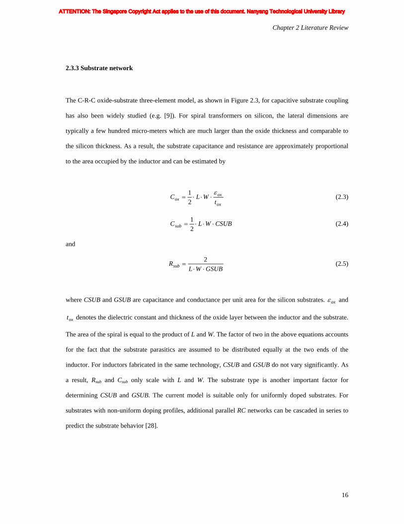
The C-R-C oxide-substrate three-element model, as shown in Figure 2.3, for capacitive substrate coupling
has also been widely studied (e.g. [9]). For spiral transformers on silicon, the lateral dimensions are
typically a few hundred micro-meters which are much larger than the oxide thickness and comparable to
the silicon thickness. As a result, the substrate capacitance and resistance are approximately proportional
to the area occupied by the inductor and can be estimated by
ox
oxox t
WLCε⋅⋅⋅=
2
1 (2.3)
CSUBWLCsub ⋅⋅⋅=2
1 (2.4)
and
GSUBWLRsub ⋅⋅
=2
(2.5)
where CSUB and GSUB are capacitance and conductance per unit area for the silicon substrates. oxε and
oxt denotes the dielectric constant and thickness of the oxide layer between the inductor and the substrate.
The area of the spiral is equal to the product of L and W. The factor of two in the above equations accounts
for the fact that the substrate parasitics are assumed to be distributed equally at the two ends of the
inductor. For inductors fabricated in the same technology, CSUB and GSUB do not vary significantly. As
a result, Rsub and Csub only scale with L and W. The substrate type is another important factor for
determining CSUB and GSUB. The current model is suitable only for uniformly doped substrates. For
substrates with non-uniform doping profiles, additional parallel RC networks can be cascaded in series to
predict the substrate behavior [28].
ATTENTION: The Singapore Copyright Act applies to the use of this document. Nanyang Technological University Library
Chapter 2 Literature Review
17
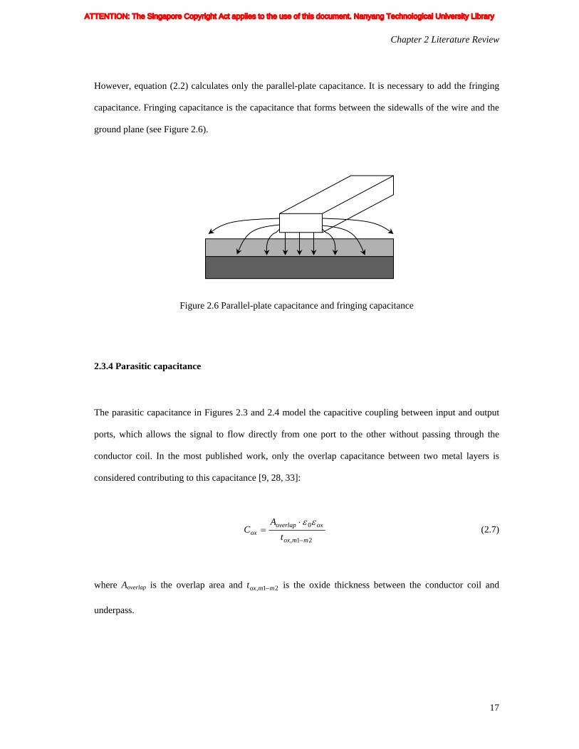
However, equation (2.2) calculates only the parallel-plate capacitance. It is necessary to add the fringing
capacitance. Fringing capacitance is the capacitance that forms between the sidewalls of the wire and the
ground plane (see Figure 2.6).
Figure 2.6 Parallel-plate capacitance and fringing capacitance
2.3.4 Parasitic capacitance
The parasitic capacitance in Figures 2.3 and 2.4 model the capacitive coupling between input and output
ports, which allows the signal to flow directly from one port to the other without passing through the
conductor coil. In the most published work, only the overlap capacitance between two metal layers is
considered contributing to this capacitance [9, 28, 33]:
21,
0
mmox
oxoverlapox t
AC
−
⋅=
εε (2.7)
where Aoverlap is the overlap area and 21, mmoxt − is the oxide thickness between the conductor coil and
underpass.
ATTENTION: The Singapore Copyright Act applies to the use of this document. Nanyang Technological University Library

Chapter 2 Literature Review
18
However, two important considerations cannot be ignored in the parasitic capacitance calculation.
Different from inductors, adjacent turns of the transformer are not equipotential; thus, the crosstalk
between adjacent turns is not negligible. The other one is the fringing capacitance, similar to the case of
the oxide capacitance calculation.
In the previous investigations, all the transformers were passive. As with all on-chip passive devices, the
passive transformers suffer from high inherent loss due to the conductive substrate as well as the thin
metal and dielectric layers. Such loss effects unavoidably limit the system performance when used for
matching networks. In order to overcome this shortcoming, the distributed active transformer (DAT) has
been proposed by Ichiro Aoki et al. [38]. By relying on extensive use of symmetric push-pull amplifiers,
AC virtual grounds, and magnetic coupling for series power combining, the DAT can achieve
simultaneous impedance transformation and power combining with lower loss and higher efficiency.
Compared to the research on spiral inductors, less work has been done on modeling of integrated
transformers. One possible reason for this may be that the transformer models are much more closely
related to their layouts and applications. Thus it is very difficult to obtain a generic, scalable transformer
model used in RF integrated circuits (RFICs) and monolithic microwave integrated circuits (MMICs),
which makes our project important. Chapter 5 will discuss about the scalable model of the interleaved
transformers in details.
ATTENTION: The Singapore Copyright Act applies to the use of this document. Nanyang Technological University Library

Chapter 3 Transformer Layout
19
Chapter 3 Transformer Layout
Accurate characterization of on-chip transformers is extremely crucial in optimizing the transformer’s
performance. It is also important for achieving a precise model to predict the behavior of on-chip
transformers over the range of operating frequency under consideration. Characterization of the
transformer based on simulation permits more flexibility during the design stage. This approach avoids the
need for test wafer tapeouts, which is time-consuming and expensive. Modifications on the layout,
geometry and process parameters of transformers can be easily achieved by creating physical models
using the software. This chapter provides an overview of the full-wave electromagnetic (EM) simulation.
Its applications, advantages in characterizing RF devices, working principles and characteristics of HFSS
are discussed. With in-depth understanding of various loss mechanisms in Si-based monolithic
transformers, a number of simulations have been setup to study the geometrical parameters’ effect on the
transformer’s performance. The EM simulations have been verified by experimental on-wafer
measurements. Hence, it provides a reliable handy design guideline for designing interleaved transformers
with optimized performance.
3.1 Transformer Structure
As discussed in Chapter 2, various geometric designs of monolithic transformers have been proposed and
many of them have been realized. In this project, we focus on the interleaved transformer, which is
constructed using conductors interwound in the same plane.
Figure 3.1 illustrates the layout of the octagonal-shaped planar transformer with a turn ratio n = 3:3. The
primary ports (Port 1 and Port 3) are located on the right side, while the secondary ports (Port 2 and Port
4) are located on the left side. The two windings are separated from each other with lateral spacing (S).
ATTENTION: The Singapore Copyright Act applies to the use of this document. Nanyang Technological University Library

Chapter 3 Transformer Layout
20
The conductor-width of each turn is named as W. As shown in Figure 3.1, the secondary winding defines
the inner radius of the transformer, denoted as IR, while the primary winding determines the outer
diameter OD. The winding scheme includes four cross-overs, two at the primary winding between P1 &
P2, and P2 & P3, another two at the secondary winding between S1 & S2, and S2 & S3.
Figure 3.1 Layout of a four-port interleaved transformer with a turn ratio n = 3:3
It should be noted that the octagonal-shaped transformers are used instead of circular- or square-shape
[39]. This is because, in the case of square-shape, the corners of the square represent a narrow place for
the current, which gives rise to current crowding effects and causes additional losses at high frequency.
Designers believe that the circular structure have the optimum performance to overcome these effects.
However, this structure is not often used because it violated rules in most mask generation systems [20].
Therefore, a polygon is used, as it is the next closest shape to circular. The performance, at the meantime,
is not being compromised significantly. An octagonal spiral has a Q-factor that is slightly lower than the
circular one but is much easier to layout. Moreover, the transformer can be easily configured as a two-
port, three-port or four-port device, when the respective ports are grounded properly, as shown in Figure
3.2. For example, when Port 3 and 4 are grounded, the transformer becomes a two-port device (see Figure
ATTENTION: The Singapore Copyright Act applies to the use of this document. Nanyang Technological University Library

Chapter 3 Transformer Layout
21
3.2 (c)). Also, it is easy to connect the transformer with other circuits in a layout, since two terminals of
one winding are on the same side.
(a)
(b)
(c)
Figure 3.2 The transformer with different port configurations: (a) four-port, (b) three-port,
and (c) two-port
3.2 HFSS (High Frequency Structure Simulator) Simulation
Ansoft HFSS is a high-performance full-wave electromagnetic (EM) field solver for passive device
modeling. One is expected to draw the structure, specify the material characteristic, and identify terminal
ATTENTION: The Singapore Copyright Act applies to the use of this document. Nanyang Technological University Library

Chapter 3 Transformer Layout
22
ports, sources, or special surface characteristics. Then parameters such as Fields, Resonant Frequency, and
S-Parameters, can be calculated.
HFSS employs a finite element method (FEM) to generate an electromagnetic field solution. The
geometric model is automatically divided into a large number of tetrahedra, where a single tetrahedron is a
four-sided pyramid. This collection of tetrahedra is referred to as the finite element mesh. Dividing a
structure into thousands of smaller regions allows the system to compute the field solution separately in
each element. The smaller the elements created by the system, the more accurate the final solution will be.
However, the size of the elements is inversely proportional to the simulation time [14].
3.2.1 Calibration of HFSS
Calibration of HFSS is a requisite for the development of a consistent, robust, and repeatable methodology
to obtain accurate simulation results. Since the transformer is essentially a magnetic coupled pair of
inductors and the structure of inductors is much simpler, the calibration of HFSS is started with inductors.
Both inductors and transformers studied in this project are based on Chartered Semiconductor
Manufacturing Ltd’s 0.18 um logic baseline process. Table 2 summarizes the technological parameters
used in the fabrication process.
Based on the process file, the simulation model is firstly built through a careful description of all the
technology layers. Individual vias are merged into a single large via to reduce the simulation time without
affecting the simulation results. Figure 3.3 shows an example of HFSS set-up of a seven-turn inductor.
ATTENTION: The Singapore Copyright Act applies to the use of this document. Nanyang Technological University Library

Chapter 3 Transformer Layout
23
Table 2 Technological Parameters
Parameter Value
Metal conductivity 4.1 e+7 S/m
Top Metal (M6) thickness 2 um
Second Metal (M5) thickness 0.54 um
HDP dielectric constant 4.2
HDP thickness 3.1 um
IMD dielectric constant 3.6
Inter-Metal thickness 8.05 um
Silicon conductivity 10 S/m
S0ilicon dielectric constant 11.9
SiN thickness 0.3 um
Figure 3.3 An example of HFSS set-up for a 7-turn inductor
ATTENTION: The Singapore Copyright Act applies to the use of this document. Nanyang Technological University Library

Chapter 3 Transformer Layout
24
Then the simulation setup is carefully examined for inductors with different dimensions. Important HFSS-
setup includes:
1. Ground return path: an appropriate current return path must be included in the simulation.
Generally, the distance between this guard ring and inductor model should follow the one on
wafer. However, it is not stated in the technology file. Through calibration, it is found to be
around 35 um (Figure 3.4).
2. Substrate thickness (tsub): for the transformer, the simulation result is not affected much as tsub
changes, which is different from the case of inductors. Since our ultimate aim is the transformer,
we fix tsub = 150 um to save simulation time.
3. Structure size: the size of the air box determines the solution space. It must be constructed in
relation to the size of the inductor model including the silicon substrate. Figure 3.5 shows the
simulated inductance curves of the inductor model in Figure 3.3 with different air box. The curve
“Simulation 1” is obtained when the simulation structure has a small air box (tair = 100 um).
Apparently, it is not accurate, especially at low frequency, where the simulated inductance is
larger than the measured one. By increasing the size of the air box, the simulated inductance
curve get closer to the corresponding measured one. Through calibration, it is found that the air
region should extend a distance around 2*tsub above the top of the inductor model and extend past
the guard ring by IR (Inner Radius of the inductor). As a result, the simulation result is in
excellent agreement with the measured data even beyond the self-resonant frequency of the
inductor (“Simulation 2” in Figure 3.5).
4. Material properties: the bulk conductivity of Si-sub is increased from 10 S/m to 14 S/m. The
dielectric constant of other isolation layers is kept the same as the one used in the foundry. Also
all metal objects have “solve inside” activated. This is because the skin depth is one tenth or
greater of the metal thickness, then explicit calculation of the volumetric current loss is required.
5. Simulation set-up: manual mesh is applied to all metal objects; in the ‘Analysis set-up’ option,
the ‘maximum delta S’ needs to be less than 0.02.
ATTENTION: The Singapore Copyright Act applies to the use of this document. Nanyang Technological University Library

Chapter 3 Transformer Layout
25
Figure 3.4 Planar view of the HFSS set-up for a 7-turn inductor
Figure 3.5 Comparisons of simulation results obtained from different HFSS set-up
ATTENTION: The Singapore Copyright Act applies to the use of this document. Nanyang Technological University Library

Chapter 3 Transformer Layout
26
Table 3 compares the measured and simulated inductance L, the peak quality-factor Q, the frequency at
which the Q-factor peaks fQmax, and the self-resonant frequency fres of the inductors. Because the measured
data is only valid up to 10GHz, the fres of DUT 1, DUT 2, DUT 4 and DUT 5 are not shown. The error of
the simulation results in the valid range compared to the measured data is always less than 5%. When
applying the calibrated simulation setup on the transformer, the simulated and measured data show a good
fit, even beyond the resonant frequency, as shown in Figure 3.6. As mentioned previously, the transformer
designed can be used as a multi-port device with respective ports grounded properly. Figure 3.6 also
displays the magnitude and phase of S21 for the transformer with both two-port and four-port
configurations.
Table 3 Comparisons of measured and simulated results of inductors
DUT # N
IR
(um)
W
(um)
S
(um)
L (nH) Max. Q fres (GHz) fQmax (GHz)
Sim./Mea. Sim./Mea. Sim./Mea. Sim./Mea.
DUT 1 3 37.5 6 2 1.40/1.43 9.2/9.1 >10 7.2/7.2
DUT 2 4 37.5 6 2 2.40/2.45 8.2/8.7 >10 4.8/4.9
DUT 3 7 37.5 6 2 7.46/7.46 7.8/7.6 8.5/8.8 2.2/2.4
DUT 4 2 50 10 2 1.02/1.04 10.4/10.4 >10 7.7/8.1
DUT 5 4 50 10 2 3.23/3.27 8.2/8.4 >10 3.0/2.9
DUT 6 7 50 10 2 9.30/9.28 6.8/6.9 5.3/5.3 1.3/1.4
ATTENTION: The Singapore Copyright Act applies to the use of this document. Nanyang Technological University Library

Chapter 3 Transformer Layout
27
-8
-6
-4
-2
0
2
4
6
8
10
0 2 4 6 8freq (GHz)
Lp (n
H)
-4
-2
0
2
4
6
8
Qp
Measured LpSimulated LpMeasured QpSimulated Qp
N=4 IR=50umW=6um S=2um
(a)
-25
-20
-15
-10
-5
0
0 2 4 6 8freq (GHz)
Mag
(S21
) (dB
)
-200
-150
-100
-50
0
50
100
150
200
Phase (deg)Measured Mag.Simulated Mag.Measured PhaseSimulated Phase
(b)
ATTENTION: The Singapore Copyright Act applies to the use of this document. Nanyang Technological University Library

Chapter 3 Transformer Layout
28
-45
-40
-35
-30
-25
-20
-15
-10
0 2 4 6 8freq (GHz)
Mag
(S21
) (dB
)
-200
-150
-100
-50
0
50
100
150
200
Phase(S21) (deg)
Measured Mag.Simulated Mag.Measured PhaseSimulated Phase
(c)
Figure 3.6 Comparisons of simulated and measured (a) L and Q of the primary coil, (b) two-port S21, and
(c) four-port S21 for a 4-turn transformer
The difference between the simulation and measurement data will become larger at high operating
frequencies. This is because differences exist between the simulated structure and its fabricated
counterpart. For example, in HFSS, vias are modeled by a large cube covering the areas comprising of all
the individual small vias in the case of a real transformer. Another possible reason is the process
parameters used in simulation are different from the actual parameters used in fabrication. However, the
optimization and characterization of transformers have been focused on the frequency range below 10
GHz in this project.
One clear advantage of the simulation-based methodology is the flexibility to perform parameter
modifications on the design to optimize the electrical behaviors or analyze the parameter sensitivity. Thus,
a VB script (Appendix 1) was written in order to generate transformers automatically with any
ATTENTION: The Singapore Copyright Act applies to the use of this document. Nanyang Technological University Library

Chapter 3 Transformer Layout
29
geometrical dimensions under consideration. In this project, Transformers with different number of turns
(N, from 2 to 5), inner radius (IR, from 30 to 140 um), metal track width (W, from 4 to 15 um), and track
spacing (S, from 1.5 to 5 um) are investigated. Most applications of interleaved transformers could be
covered by such range of layout parameters.
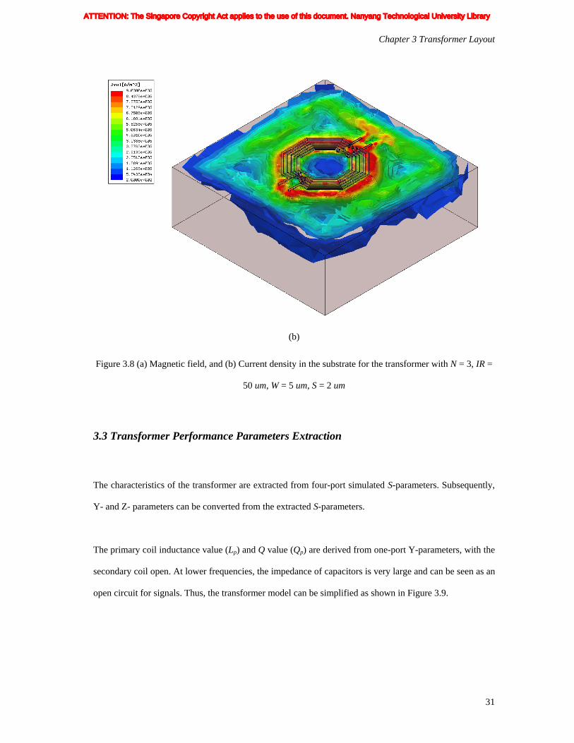
It is very interesting that HFSS could provide a graphical view of how the magnetic field behaves around
the transformer structure. Figure 3.7 displays both the magnetic field and current density distribution along
the conductors for the transformer with N = 3, IR = 50 um, W = 5 um, S = 2 um. It is clear that closer to the
surface of the conductor, the magnetic field becomes stronger (Figure 3.7 (a)). Similarly, the current
density also increases nearer to the surface due to the skin and proximity effects (Figure 3.7 (b)). As
mentioned in Chapter 2, the magnetic field induced by the transformer current penetrates into the substrate
and cause eddy current flow inside the substrate. This also can be shown by HFSS (see Figure 3.8). In
Figure 3.8, we can see that both the magnetic field and current density inside the substrate has a much
lower magnitude compared to the one in the transformer conductor. However, they cannot be ignored
since they will largely degrade the transformer’s performance.
(a)
ATTENTION: The Singapore Copyright Act applies to the use of this document. Nanyang Technological University Library

Chapter 3 Transformer Layout
30
(b)
Figure 3.7 (a) Magnetic field, and (b) current density along the conductor for the transformer with N = 3,
IR = 50 um, W = 5 um, S = 2 um
(a)
ATTENTION: The Singapore Copyright Act applies to the use of this document. Nanyang Technological University Library
Chapter 3 Transformer Layout
31
(b)
Figure 3.8 (a) Magnetic field, and (b) Current density in the substrate for the transformer with N = 3, IR =
50 um, W = 5 um, S = 2 um
3.3 Transformer Performance Parameters Extraction
The characteristics of the transformer are extracted from four-port simulated S-parameters. Subsequently,
Y- and Z- parameters can be converted from the extracted S-parameters.
The primary coil inductance value (Lp) and Q value (Qp) are derived from one-port Y-parameters, with the
secondary coil open. At lower frequencies, the impedance of capacitors is very large and can be seen as an
open circuit for signals. Thus, the transformer model can be simplified as shown in Figure 3.9.
ATTENTION: The Singapore Copyright Act applies to the use of this document. Nanyang Technological University Library

Chapter 3 Transformer Layout
32
Figure 3.9 Simplified model for transformers at lower frequencies
We can easily determines that
w
YagL
)(Im 111
1
−
= (3.1)
w
YagL
)(Im 122
2
−
= (3.2)
Similar approach applies to the extraction of secondary coil parameters. The method of extraction for the
transformer parameters such as the mutual inductance coupling coefficient K, and the transmission
coefficient, |S21| in dB, the maximum available gain of the transformer Gmax, together with primary and
secondary coil characteristics, are illustrated in Table 4. These quantities are used to evaluate the
transformer’s performance.
Port 1
L1 L2
R1 R2
Port 2 M
ATTENTION: The Singapore Copyright Act applies to the use of this document. Nanyang Technological University Library

Chapter 3 Transformer Layout
33
Table 4 Transformer Performance Parameters Extraction
w
YagpL
)111(Im −
= Evaluated with Port 3 and Port 4 grounded, and
Port 2 open (One port extraction)
)111(Re
)111(Im
−
−−=
Yal
YagpQ
w
Yag
sL)1
22(Im −=
Evaluated with Port 3 and Port 4 grounded, and
Port 1 open (One port extraction)
)122(Re
)122(Im
−
−−=
Yal
YagsQ
)22(Im)11(Im
2))21((Im
ZagZag
Zag
SLPL
MK
⋅=
⋅=
Evaluated with both Port 3 and Port 4 are
grounded
Note:
21122
22
22
2
111
SS
SSk
⋅
Δ+−−= ,
21122211
SSSS ⋅−⋅=Δ
S21
)12(12
21max −−= kk
S
SG
ATTENTION: The Singapore Copyright Act applies to the use of this document. Nanyang Technological University Library

Chapter 4 Characterization
34
Chapter 4 Characterization of On-Chip Transformers
This chapter aims to discuss the impact of the transformer’s physical dimensions on the performance of
Si-based interleaved transformers. The number of turns (N), the inner radius (IR), track width (W), and
turn-to-turn spacing (S) were varied to find the optimized geometry and to study the resultant changes on
the transformer’s performance, such as the quality factor Q, self-inductance L, the coupling factor K, the
maximum available gain Gmax and the resonant frequency fres. The conclusion of the investigation can be
used as guidelines for on-chip transformers design.
4.1 Effects of the Transformer’s Physical Dimensions
The impacts of geometrical parameters on the transformer behaviors are closely related to the loss
mechanisms discussed previously. In this section, effects of geometrical parameters (N, IR, W, and S) on
the performance of integrated transformers in terms of the coupling factor K, and the maximum available
gain of the transformer Gmax, are investigated. In addition, as the transformer is formed by interwinding
two identical spiral inductors, their effects on the quality factor Qp, the self-inductance Lp, and the
resonant frequency fres of the primary winding are also examined in this section.
4.1.1 Number of turns (N)
Self-inductance and quality-factor values related to frequency are illustrated in Figures 4.1 (a) and (b).
Characteristics of the primary winding are set as identical except the number of turns. As N varies from 2
to 5, the inductance value increases, while the Q-factor and the resonant frequency decreases (the
resonance frequency of transformers with N = 2 is beyond 14 GHz and not shown in the graph).
ATTENTION: The Singapore Copyright Act applies to the use of this document. Nanyang Technological University Library

Chapter 4 Characterization
35
-8
-6
-4
-2
0
2
4
6
8
10
0 2 4 6 8 10freq (GHz)
Qp
N=2N=3N=4N=5
IR=50umW=6umS=2um
(a)
-20
-15
-10
-5
0
5
10
15
20
0 2 4 6 8 10 12 14freq (GHz)
Lp (n
H)
N=2N=3N=4N=5
IR=50umW=6umS=2um
(b)
Figure 4.1 (a) Qp and (b) Lp versus frequency for varying number of turns
As depicted in Figure 4.1 (b), the value of Lp increases about 10 times, from 0.45 nH to 5.27 nH. This
increase is due to stronger magnetic field induced by more windings and hence more constructive mutual
inductance. The mutual inductances between adjacent segments of the spiral are positive as the current
ATTENTION: The Singapore Copyright Act applies to the use of this document. Nanyang Technological University Library

Chapter 4 Characterization
36
directions are the same, while inductances between parallel segments on opposite sides are negative (see
Figure 4.2).
Figure 4.2 Positive and negative mutual inductance components in the primary coil [24]
At frequencies well below the maximum Q value for the primary winding, the shunt parasitics of the
transformer have little effect and consequently the inductive reactance and Qp increases with frequency.
However, with the increasing frequency, the dissipation of energy in the semi-conducting substrate and the
ac resistance of the metallization begin to increase faster than the inductive reactance. Thus, the Q-factor
experiences a bell- shape curve peaking at Qp, max [32]. Different from Lp, Qp decreases with N. This is
because as N becomes larger, the total physical length increases, which translates to a larger series
resistance value. Also larger area under the metal line means greater parasitic oxide and substrate
capacitances. All these effects cause the degradation of Q. Besides degradation in Q, the cost of increasing
inductance and coupling factor is at the expense of larger chip area and drop in fres. The area consumption
of the transformer with N = 5 is about 4 times of that of the one-turn transformer. In addition, the fres of the
one-turn transformer is around 50 GHz. But this value decreases to 5 GHz for the transformer with N = 5.
Therefore, if high frequency application is required, the five-turn transformer cannot be used.
ATTENTION: The Singapore Copyright Act applies to the use of this document. Nanyang Technological University Library

Chapter 4 Characterization
37
0.5
0.6
0.7
0.8
0.9
1
0.1 0.3 0.5 0.7 0.9 1.1 1.3 1.5 1.7 1.9 2.1
freq (GHz)
K
N=2N=3N=4N=5
Figure 4.3 K versus frequency for varying N
0
0.1
0.2
0.3
0.4
0.5
0.6
0.7
0.8
0.9
0 2 4 6 8 10
freq (GHz)
Gm
ax
N=2N=3N=4N=5
IR=50umW=6umS=2um
Figure 4.4 Gmax versus frequency for varying N
Since the materials used in the fabrication of an IC chip have magnetic properties similar to air, there is
imperfect confinement of the magnetic flux in a monolithic transformer. Thus, the coupling factor K of the
transformer is always less than 1. As frequency increases, the magnetic coupling between primary and
ATTENTION: The Singapore Copyright Act applies to the use of this document. Nanyang Technological University Library

Chapter 4 Characterization
38
secondary coils becomes stronger. Therefore, the K-factor also increases, as shown in Figure 4.3. Besides,
larger number of turns increases the magnetic and electric coupling between primary and secondary coils,
which leads to an increase in K. Figure 4.4 shows how Gmax changes as N varies. At low frequency, Gmax
improves a lot when N increases. However, this reverses at high frequencies due to the presence of larger
series resistance and parasitic effects.
From the previous discussion, it can be concluded that it is very crucial for circuit designers to choose
proper inductance value with acceptable quality factor and S21 (or Gmax) to optimize the circuit
performance. Generally, the maximum Q value is more technology than geometry dependent, which
means, the thickness and conductivity of top metal layer highly affect the result. On the contrary,
inductance values are more geometry dependent. The data shown in previous figures indicates that a
design with 3 to 4 turns is optimum. If larger number of turns is used, more chip area will be taken.
4.1.2 Inner radius (IR)
Inner radius (IR) of the transformer is another important parameter that has significant influences on the
transformer’s performance. IR and N determine the total chip area occupied by the device. Figure 4.5 (a)
shows how the self-inductance Lp changes with respect to IR. As IR increases, Lp improves due to the
increase in the conductor length. Therefore, different inductance values can be achieved by choosing
appropriate IR. However, as IR increases, a larger chip area is taken by the transformer, which leads to
more fabrication cost. In addition, undesirable parasitic oxide and substrate capacitances increase when
more area occupied by the transformer; thus, fres decreases with IR.
At low frequency, transformers with larger IR have greater Q. As IR decreases, Q also decreases
gradually. This decrease is related to the distance (or gap) between opposite sides at the center of the
spiral. For transformers with smaller IR, the distance between opposite sides of the conductor shrinks,
ATTENTION: The Singapore Copyright Act applies to the use of this document. Nanyang Technological University Library
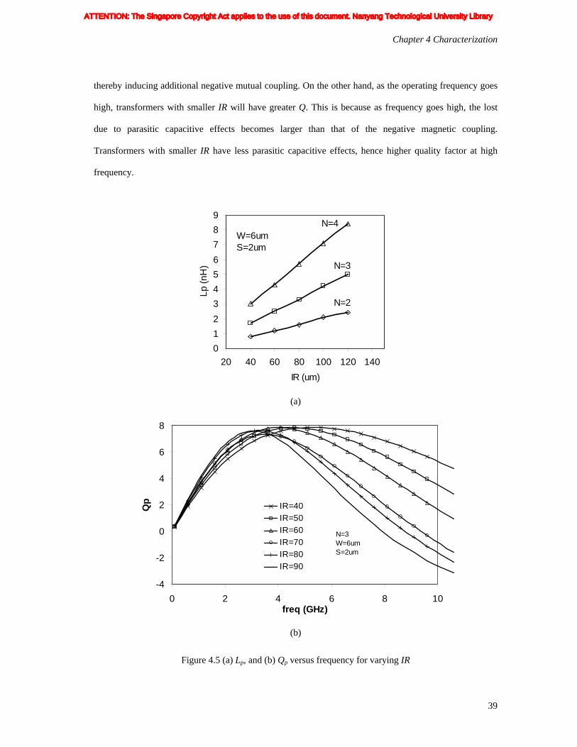
Chapter 4 Characterization
39
thereby inducing additional negative mutual coupling. On the other hand, as the operating frequency goes
high, transformers with smaller IR will have greater Q. This is because as frequency goes high, the lost
due to parasitic capacitive effects becomes larger than that of the negative magnetic coupling.
Transformers with smaller IR have less parasitic capacitive effects, hence higher quality factor at high
frequency.
0123456789
20 40 60 80 100 120 140IR (um)
Lp (n
H)
W=6umS=2um
N=4
N=3
N=2
(a)
-4
-2
0
2
4
6
8
0 2 4 6 8 10freq (GHz)
Qp IR=40
IR=50IR=60IR=70IR=80IR=90
N=3W=6umS=2um
(b)
Figure 4.5 (a) Lp, and (b) Qp versus frequency for varying IR
ATTENTION: The Singapore Copyright Act applies to the use of this document. Nanyang Technological University Library
Chapter 4 Characterization
40
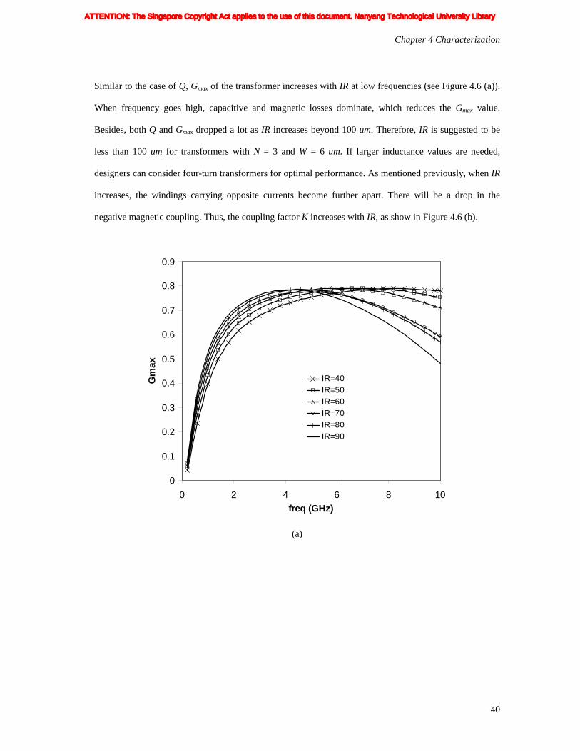
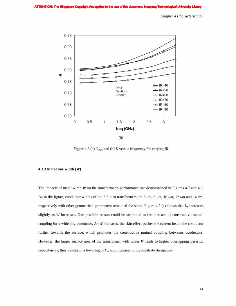
Similar to the case of Q, Gmax of the transformer increases with IR at low frequencies (see Figure 4.6 (a)).
When frequency goes high, capacitive and magnetic losses dominate, which reduces the Gmax value.
Besides, both Q and Gmax dropped a lot as IR increases beyond 100 um. Therefore, IR is suggested to be
less than 100 um for transformers with N = 3 and W = 6 um. If larger inductance values are needed,
designers can consider four-turn transformers for optimal performance. As mentioned previously, when IR
increases, the windings carrying opposite currents become further apart. There will be a drop in the
negative magnetic coupling. Thus, the coupling factor K increases with IR, as show in Figure 4.6 (b).
0
0.1
0.2
0.3
0.4
0.5
0.6
0.7
0.8
0.9
0 2 4 6 8 10freq (GHz)
Gm
ax
IR=40IR=50IR=60IR=70IR=80IR=90
(a)
ATTENTION: The Singapore Copyright Act applies to the use of this document. Nanyang Technological University Library
Chapter 4 Characterization
41
(b)
Figure 4.6 (a) Gmax and (b) K versus frequency for varying IR
4.1.3 Metal line width (W)
The impacts of metal width W on the transformer’s performance are demonstrated in Figures 4.7 and 4.8.
As in the figure, conductor widths of the 3:3-turn transformers are 6 um, 8 um, 10 um, 12 um and 14 um,
respectively with other geometrical parameters remained the same. Figure 4.7 (a) shows that Lp increases
slightly as W increases. One possible reason could be attributed to the increase of constructive mutual
coupling for a widening conductor. As W increases, the skin effect pushes the current inside the conductor
further towards the surface, which promotes the constructive mutual coupling betweens conductors.
However, the larger surface area of the transformer with wider W leads to higher overlapping parasitic
capacitances; thus, results in a lowering of fres and increases in the substrate dissipation.
0.63
0.68
0.73
0.78
0.83
0.88
0.93
0.98
0 0.5 1 1.5 2 2.5 3
freq (GHz)
IR
IR=40IR=50IR=60IR=70IR=80IR=90
N=3 W=6um S=2um
ATTENTION: The Singapore Copyright Act applies to the use of this document. Nanyang Technological University Library
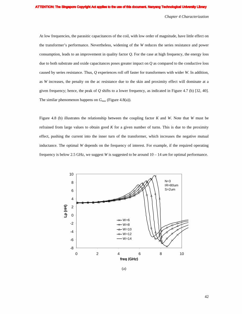
Chapter 4 Characterization
42
At low frequencies, the parasitic capacitances of the coil, with low order of magnitude, have little effect on
the transformer’s performance. Nevertheless, widening of the W reduces the series resistance and power
consumption, leads to an improvement in quality factor Q. For the case at high frequency, the energy loss
due to both substrate and oxide capacitances poses greater impact on Q as compared to the conductive loss
caused by series resistance. Thus, Q experiences roll off faster for transformers with wider W. In addition,
as W increases, the penalty on the ac resistance due to the skin and proximity effect will dominate at a
given frequency; hence, the peak of Q shifts to a lower frequency, as indicated in Figure 4.7 (b) [32, 40].
The similar phenomenon happens on Gmax (Figure 4.8(a)).
Figure 4.8 (b) illustrates the relationship between the coupling factor K and W. Note that W must be
refrained from large values to obtain good K for a given number of turns. This is due to the proximity
effect, pushing the current into the inner turn of the transformer, which increases the negative mutual
inductance. The optimal W depends on the frequency of interest. For example, if the required operating
frequency is below 2.5 GHz, we suggest W is suggested to be around 10 – 14 um for optimal performance.
-8
-6
-4
-2
0
2
4
6
8
10
0 2 4 6 8 10freq (GHz)
Lp (n
H)
W=6W=8W=10W=12W=14
N=3IR=80umS=2um
(a)
ATTENTION: The Singapore Copyright Act applies to the use of this document. Nanyang Technological University Library
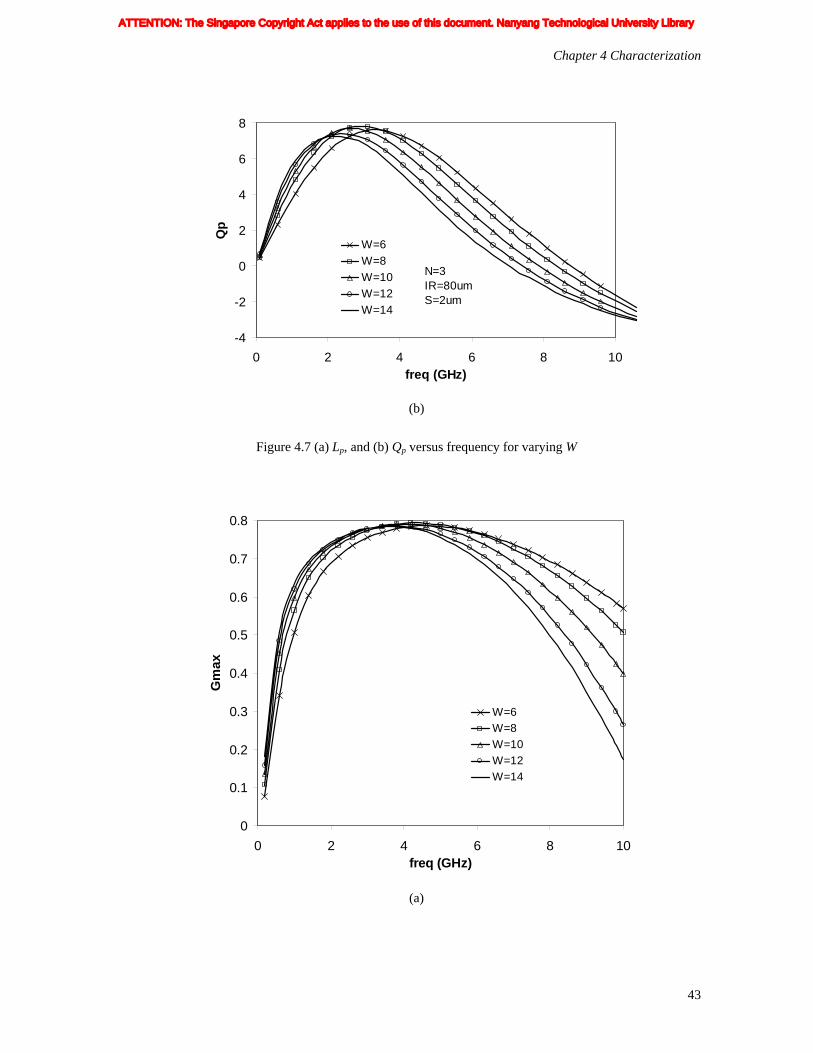
Chapter 4 Characterization
43
-4
-2
0
2
4
6
8
0 2 4 6 8 10freq (GHz)
Qp
W=6W=8W=10W=12W=14
N=3IR=80umS=2um
(b)
Figure 4.7 (a) Lp, and (b) Qp versus frequency for varying W
0
0.1
0.2
0.3
0.4
0.5
0.6
0.7
0.8
0 2 4 6 8 10freq (GHz)
Gm
ax
W=6W=8W=10W=12W=14
(a)
ATTENTION: The Singapore Copyright Act applies to the use of this document. Nanyang Technological University Library
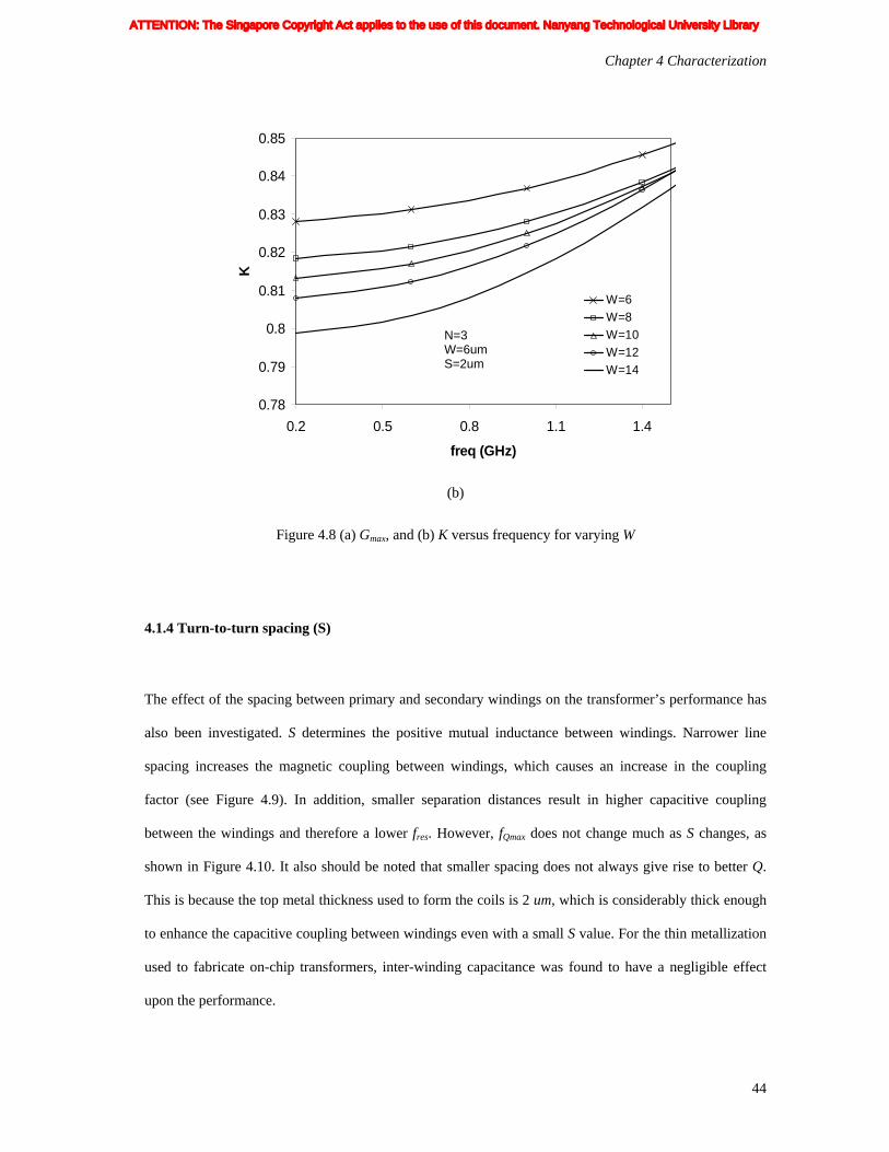
Chapter 4 Characterization
44
(b)
Figure 4.8 (a) Gmax, and (b) K versus frequency for varying W
4.1.4 Turn-to-turn spacing (S)
The effect of the spacing between primary and secondary windings on the transformer’s performance has
also been investigated. S determines the positive mutual inductance between windings. Narrower line
spacing increases the magnetic coupling between windings, which causes an increase in the coupling
factor (see Figure 4.9). In addition, smaller separation distances result in higher capacitive coupling
between the windings and therefore a lower fres. However, fQmax does not change much as S changes, as
shown in Figure 4.10. It also should be noted that smaller spacing does not always give rise to better Q.
This is because the top metal thickness used to form the coils is 2 um, which is considerably thick enough
to enhance the capacitive coupling between windings even with a small S value. For the thin metallization
used to fabricate on-chip transformers, inter-winding capacitance was found to have a negligible effect
upon the performance.
0.78
0.79
0.8
0.81
0.82
0.83
0.84
0.85
0.2 0.5 0.8 1.1 1.4
freq (GHz)
K
W=6W=8W=10W=12W=14
N=3 W=6um S=2um
ATTENTION: The Singapore Copyright Act applies to the use of this document. Nanyang Technological University Library
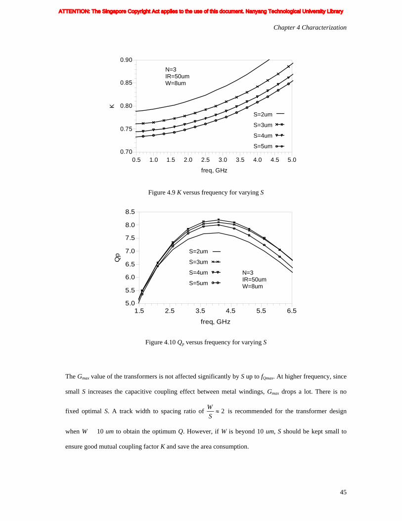
Chapter 4 Characterization
45
Figure 4.9 K versus frequency for varying S
Figure 4.10 Qp versus frequency for varying S
The Gmax value of the transformers is not affected significantly by S up to fQmax. At higher frequency, since
small S increases the capacitive coupling effect between metal windings, Gmax drops a lot. There is no
fixed optimal S. A track width to spacing ratio of 2≈S
W is recommended for the transformer design
when W � 10 um to obtain the optimum Q. However, if W is beyond 10 um, S should be kept small to
ensure good mutual coupling factor K and save the area consumption.
S=2um
S=3um
S=4um
S=5um
2.5 3.5 4.5 5.51.5 6.5
5.5
6.0
6.5
7.0
7.5
8.0
5.0
8.5
freq, GHz
Qp
N=3 IR=50um W=8um
1.0 1.5 2.0 2.5 3.0 3.5 4.0 4.50.5 5.0
0.75
0.80
0.85
0.70
0.90
freq, GHz
K
N=3 IR=50um W=8um
S=2um
S=3um
S=4um
S=5um
ATTENTION: The Singapore Copyright Act applies to the use of this document. Nanyang Technological University Library

Chapter 4 Characterization
46
The information extracted from these graphs is summarized concisely in Table 5. It can be used to provide
useful guidelines for on-chip transformer designs.
Table 5 Interleaved Transformer Performance Trends
Note: �: increase, ��: increase first, then decrease, �: decrease, ��: almost constant
4.2 Design Methodology
As a first step, the inductance required for each winding must be determined from consideration of center
frequency specification. For example, an inductance value of 3.3 nH is needed for an application at 3
GHz. Figure 4.11 illustrates the design procedure for this design example. From previous discussion, N
and IR are two main factors determining the inductance value. Since the transformer is designed to work at
3 GHz, its self-resonant frequency, fres, must be well above 3 GHz. Generally, fres is chosen to be at least
three times of the working frequency required, which means fres � 9 GHz in this design example. Figure
4.2 (b) shows that transformers with N � 3 can fulfill this requirement. This is Step 1 in the flow chart.
Then refer to Figure 4.5 (a), a 3.3-nH inductance can be achieved when IR = 80 um and N = 3 (Step 2 in
Figure 4.11). If N = 2 is used, IR has to be very large to achieve the desired inductance value, thereby
consuming more chip area.
Qmax L fres K
(extracted at low f)
N � � � � �
IR � �� � � �
W � �� � � �
S � �� � � �
ATTENTION: The Singapore Copyright Act applies to the use of this document. Nanyang Technological University Library
Chapter 4 Characterization
47
Q is another important consideration. In Figure 4.12, the contour curves represent the values of Q which
are plotted as a function of IR and W. Each point on the contour plot corresponds to a specific transformer
layout design, which is defined by the parameter set (N, IR, W, and S). Here, for simplicity, only results
for transformers with N = 3 and S = 2 um are shown. The contour plots can identify the optimal layout for
a given technology at a frequency of interest.
At low frequencies, such as 600 MHz shown in Figure 4.12 (a), larger IR and W result in higher Q. As the
frequency increases to 3 GHz, the substrate loss self-resonance effects become important for transformers
with larger W. Thus, the Q contours begin to roll-off. For the design example, it is obvious that the highest
Q achievable for a 3.3nH-inductance is around 7.6 when W = 10 um. However, for the case at 1.6 GHz, a
metal width of 10 um is not optimum. It should be a bit wider.
The last geometrical parameter needs to be determined is the tracking spacing S. In fact, the transformer
design involves a complex trade-off between various layout parameters. If a high K-factor is also required,
S has to be kept small (for example, 2 um) to ensure high mutual coupling between conductors. However,
by choosing S closes to half of the metal width, an even higher Q can be achieved.
Knowing the number of turns, inner radius, metal width and spacing, it is possible to estimate the initial
size of the transformer required. However, because of the complexity of high frequency phenomenon and
distributed structure of the transformer, structure simulations should be involved in the design procedure.
By doing so, it can be confirmed that the original performance requirements are satisfied. If the simulation
result meets the design specifications, all the geometrical parameters will pass down to the scalable model
to generate the netlist for the circuit design. Otherwise, if the simulation does not fulfill the design
requirement, the selection of geometrical parameters will start from Step 1 again omitting the choices we
have made in the previous selection, as shown in Figure 4.11.
ATTENTION: The Singapore Copyright Act applies to the use of this document. Nanyang Technological University Library

Chapter 4 Characterization
48
Figure 4.11 The design flowchart
(a)
Step 1: Fig. 3 (a) Check for f
Step 2: Fig. 4 (a) Check for L
N
IR
Step 3: Fig. 8 Check for Q W & S
Scalable Model
EM tools (e.g. HFSS)
Yes
Netlist
Design Specifications: L & f
No
Confirm
ATTENTION: The Singapore Copyright Act applies to the use of this document. Nanyang Technological University Library
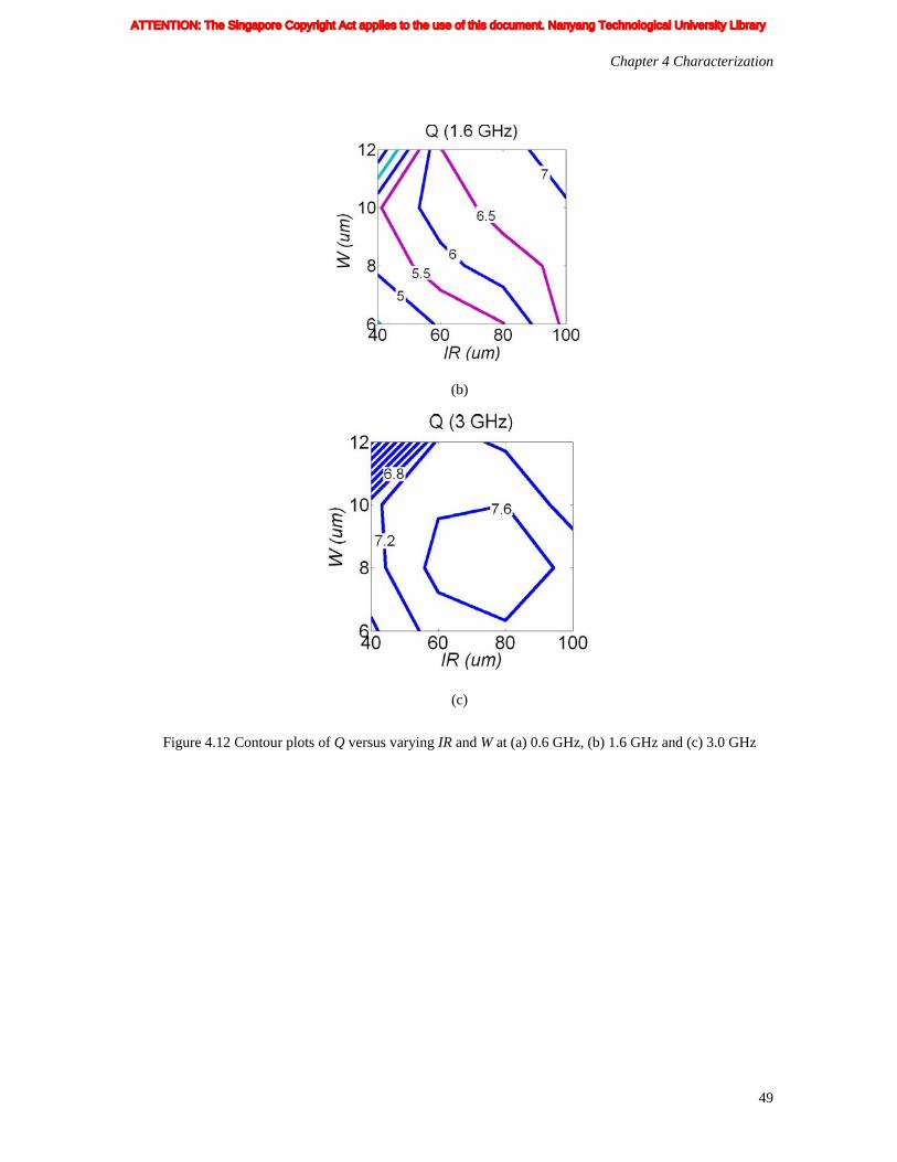
Chapter 4 Characterization
49
(b)
(c)
Figure 4.12 Contour plots of Q versus varying IR and W at (a) 0.6 GHz, (b) 1.6 GHz and (c) 3.0 GHz
ATTENTION: The Singapore Copyright Act applies to the use of this document. Nanyang Technological University Library

Chapter 5 Modeling
50
Chapter 5 Modeling
The distributed structure of spiral transformers together with the complexity of all the parasitic components
makes it difficult to estimate both L and Q of the transformer. Therefore, an accurate and scalable model is
needed to understand the effects of the parasitics and their impact on the overall transformer performance.
Scalability implies that the component values of the transformer model can be extracted from geometric
and technological parameter specifications. By employing lumped RLC elements, the proposed equivalent
circuit model provides the capability of efficiently representing the electrical performance of the
transformer, as well as the compatibility with other design components.
Developing a compact model involves a fitting process. During model development, some model
parameters are introduced, which need to be lately determined through curve fitting based on the simulation
results from HFSS. However, we firstly have to construct an appropriate circuit topology.
5.1 Generation of Transformer Model
The equivalent circuit of the transformer is proposed based on the lumped circuit model of a spiral
inductor. Essentially, the transformer is simply a magnetic coupled pair of spiral inductors. Lots of research
work has been done on developing the equivalent model for on-chip inductors [24, 27, 28, 32].
Figure 5.1 shows the 2-� equivalent circuit of inductors. For a single metal line, the dc current is uniformly
distributed inside the conductor. Therefore, the inductance and resistance of the metal line and underpass is
represented by the series inductance and resistance. However, as frequency increases, the current density
becomes non-uniform. The skin effect pushes the ac current toward the surface of the conductor. To
capture the effect of different current densities in different conduction layers, additional RL branches are
introduced in parallel to the series resistance to represent each conduction layer in depth. By adding more
ATTENTION: The Singapore Copyright Act applies to the use of this document. Nanyang Technological University Library

Chapter 5 Modeling
51
ladder branches, the skin effect can be accurately modeled up to an arbitrary maximum frequency. For
model simplicity, only one RL branch is brought into the circuit, which models the surface layer resistance
and inductance [24]. Then the ladder circuit is split into two parts to indicate the presence of the center-tap.
The series capacitance, Cs models the parasitic capacitive coupling between input and output ports of the
primary/secondary winding. This capacitance allows the signal to flow directly from the input to output
port without passing through the spiral conductor.
Figure 5.1 2-� model of the primary winding
The substrate effect is modeled by a three-element network comprised of Cox, Rsub and Csub. Cox represents
the oxide capacitance whereas Rsub and Csub represent the silicon substrate resistance and capacitance,
respectively. The physical origin of Rsub is the silicon conductivity which is predominately determined by
the majority carrier concentration. Csub models the high-frequency capacitive effects occurring in the
semiconductor, as discussed in Chapter 4.
It should be noted that the loss due to eddy currents in the underlying substrate, induced by the penetration
of the magnetic field into the conductive silicon is not included in our model. This is because the loss is
substantial when substrate resistivity is low (e.g., < 1 �-cm). The case of less conductive substrate (e.g., >
ATTENTION: The Singapore Copyright Act applies to the use of this document. Nanyang Technological University Library
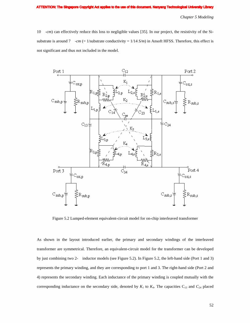
Chapter 5 Modeling
52
10 �-cm) can effectively reduce this loss to negligible values [35]. In our project, the resistivity of the Si-
substrate is around 7 �-cm (= 1/substrate conductivity = 1/14 S/m) in Ansoft HFSS. Therefore, this effect is
not significant and thus not included in the model.
Figure 5.2 Lumped-element equivalent-circuit model for on-chip interleaved transformer
As shown in the layout introduced earlier, the primary and secondary windings of the interleaved
transformer are symmetrical. Therefore, an equivalent-circuit model for the transformer can be developed
by just combining two 2-� inductor models (see Figure 5.2). In Figure 5.2, the left-hand side (Port 1 and 3)
represents the primary winding, and they are corresponding to port 1 and 3. The right-hand side (Port 2 and
4) represents the secondary winding. Each inductance of the primary winding is coupled mutually with the
corresponding inductance on the secondary side, denoted by K1 to K4. The capacities C13 and C24 placed
ATTENTION: The Singapore Copyright Act applies to the use of this document. Nanyang Technological University Library

Chapter 5 Modeling
53
across windings to model the parasitic capacitive coupling between different ports within the same coil.
Such capacitive coupling allows the signal to flow directly from one winding to the other without passing
through the conductor coil. Other capacities Cps, C12, C34, C14 and C23 model the distributed capacitive
coupling across two coils. Based on the transformer’s structure, both the crosstalk between adjacent turns
and the overlap between the spiral and the underpass contribute to these parasitic capacitances.
5.2 Analytical RLC Element Calculations
5.2.1 Inductance calculation
The most critical and difficult value to be calculated among all the components is the value of inductance.
It can be computed exactly by solving Maxwell’s equations. In this project we use a simple and accurate
expression from [41]:
⎥⎥⎦
⎤
⎢⎢⎣
⎡++= 2
43)2ln(2
12
ρρρ
μcc
ccavgdn
dcL (5.1)
Here, 1
c = 1.07, 2c = 2.29, 3c = 0, and 4c = 0.19 for the octagonal shape. If other transformer structure
is used, the value of i
c will be different.
This formula is derived from electromagnetic principles by approximating the sides of the spirals by
symmetrical current sheets of equivalent current densities. The current sheets on opposite sides are parallel
to one another, whereas the adjacent ones are orthogonal. Using symmetry and the fact that sheets have
zero mutual inductance, the computation of the inductance is now reduced by evaluating the self-
inductance of one sheet and the mutual inductance between opposite current sheets. These self-and mutual
ATTENTION: The Singapore Copyright Act applies to the use of this document. Nanyang Technological University Library

Chapter 5 Modeling
54
inductances are evaluated by using the concepts of geometric mean distance (GMD), arithmetic mean
distance (AMD), and arithmetic mean square distance [42, 43].
The accuracy of this expression worsens as the ratio of S / W becomes large, it exhibits a maximum error of
8% of S � 3W. The reason is that a smaller spacing improves the interwinding magnetic coupling and
reduces the area consumed by the spiral. A large spacing is only desired to reduce the interwinding
capacitance.
It also should be noted that this formula is not suitable for the case of a one-turn transformer. This is
because the coefficients ci in the formula take account the effect of geometrical dimensions (for example, S)
on the value of the self-inductance. But there is no “spacing” existing between the primary or secondary
winding as each winding has only 1 turn. Therefore, this formula is no longer accurate for N = 1.
Since the transformer is symmetrical, we can get corresponding (Figure 5.2)
2
,,3,1
pdcL
pLpL == (5.1)
2,
,3,1sdcL
sLsL == (5.2)
5.2.2 Ladder circuit elements calculation [14]
Instead of resorting to numerical or purely empirical techniques [12, 33] to determine the values of the
ladder circuit ( 1R , 1L , 0R and 0L ), Cao et al. have derived the closed-form frequency-independent
solution for each element based on the underlying physics [24].
1) Metal Layer Partition: Since R1 L1 models the metal surface layer and R0 L0 models the overall
conductor, their relationship is uniquely defined upon selecting a partition ratio for the outer layer to the
ATTENTION: The Singapore Copyright Act applies to the use of this document. Nanyang Technological University Library

Chapter 5 Modeling
55
overall cross section. As shown in Figure 5.1, an empirically optimized condition from [44] can be
expressed as
0
1
1
0 315.0R
R
L
L⋅= (5.3)
2) Electromagnetic Analysis of R(f): The physical constraint of R(f) is obtained from [24] and shown
below:
2210 mcrit LmwRR = (5.4)
and 23.1
240
Nm =
, where m is a new parameter introduced to model the dependence on the number of turns.
Here, mL describes the mutual inductance between 0L and 1L , since the inductance 0L is induced by the
magnetic field in the adjacent space of the line. As increasing numbers of parallel lines, metal resistance
shows more significant frequency dependence. And critw is the frequency at which the current crowding
effects become significant [35]:
sheetcrit Rw
Pw ⋅⋅=
20
1.3
μ (5.5)
where P is the metal pitch and t
R CuAlsheet
−=ρ
.
3) Relationship of LC at High Frequency: From Maxwell’s equations, L and C in the metal-oxide-silicon
system at extremely high frequencies is related as
22 cL
CLox
GML
hfhf ε= (5.6)
ATTENTION: The Singapore Copyright Act applies to the use of this document. Nanyang Technological University Library

Chapter 5 Modeling
56
where c is the speed of light in a vacuum and oxε is the dielectric constant of silicon oxide.
As the ladder circuit model shows
1
2
0010
2
)1(L
LLL
LL
LL mm
hf −=⋅−= (5.7)
10LLkLm = (5.8)
In fact, the coupling factor k of an inductor is very small, less than 0.02. Thus, we ignore mL in our model.
Cox is similar to a parallel-plate capacitance. If we assume it is proportional to the effective area occupied
by the ac current in the inductor, then hfC scales with the resistance when the current is pushed to the edge
of the metal line due to proximity effect, which means
1
0
)(
)(
R
R
R
R
dcAreaCurrent
acAreaCurrent
C
C
hf
dc
ox
hf ≈== (5.9)
oxhf CR
RC ⋅=
1
0 (5.10)
By substituting (5) and (6) into (4), we get
2
2
1
0
1
2
06
)(c
LC
R
R
L
LL GMLox
oxm ⋅
=⋅⋅−ε
(5.11)
where the factor of 6 is a parameter fitted from measurement in order to improve the accuracy.
(4) Resistance and Inductance at Low Frequency: At low frequency, the ladder circuit should be equivalent
to dcR and dcL in series. Thus, we obtain the following two conditions from circuit theory:
ATTENTION: The Singapore Copyright Act applies to the use of this document. Nanyang Technological University Library
Chapter 5 Modeling
57
10
1010 ||
RR
RRRRRdc +
== (5.12)
12
10
001100 )()](||[ L
RR
RLjwLRRimagLLdc +
+≈++= (5.13)
Assuming 01 RnR ⋅= , the ladder circuit elements 0R , 0L , 1R , and 1L can be solved in closed forms from
equations (5.3), (5.4) and (5.9)-(5.13). Cao’s approach demonstrates good scalability and flexibility, thus, it
is adopted in our model. However, it is assumed that n » 1 to simplify the derivation in [24], which does
not fit into our transformer design. Further modifications need to be performed to the equation. For
example, n is found to be within a range of 1 – 6 for the transformers investigated (2 � N � 5, 30 � IR �
140 um, 4 �W � 15 um, and 1.5 � S � 2 um). Revising the derivation, 0L should be calculated as
)2)1(315.0
11(0
+⋅⋅−⋅=
nndcLL (5.14)
Also the solution for n could be simplified as (5.15)
2
2
GMLox
dcox
L
cLCn
εα ⋅
= (5.15)
where Cox is similar as a parallel-plate capacitance, c is the speed of light, oxε is the relative permittivity of
silicon oxide, LGML is the geometrical mean length of the conductor and the factor of � (instead of 6 used in
[24]) is a fitting parameter.
ATTENTION: The Singapore Copyright Act applies to the use of this document. Nanyang Technological University Library
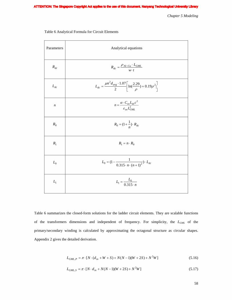
Chapter 5 Modeling
58
Table 6 Analytical Formula for Circuit Elements
Parameters Analytical equations
dcR tw
LR GMLCuAl
dc ⋅⋅
= −ρ
dcL ⎥⎦
⎤⎢⎣
⎡+
⋅= 2
2
19.0)29.2
ln(2
07.1ρ
ρμ avg
dc
dnL
n 2
2
GMLox
dcox
L
cLCn
εα ⋅
=
0R dcRn
R ⋅+= )1
1(0
1R 01 RnR ⋅=
0L dcLnn
L ⋅+⋅⋅
−= ))1(315.0
11(
20
1L n
LL
⋅=
315.00
1
Table 6 summarizes the closed-form solutions for the ladder circuit elements. They are scalable functions
of the transformers dimensions and independent of frequency. For simplicity, the LGML of the
primary/secondary winding is calculated by approximating the octagonal structure as circular shapes.
Appendix 2 gives the detailed derivation.
])2)(1()([ 2, WNSWNNSWdNL inPGML ++−+++⋅⋅= π (5.16)
])2)(1([ 2, WNSWNNdNL inSGML ++−+⋅⋅= π (5.17)
ATTENTION: The Singapore Copyright Act applies to the use of this document. Nanyang Technological University Library

Chapter 5 Modeling
59
5.2.3 Substrate network
Besides the skin and proximity effects, the capacitive substrate coupling is another important effect to be
considered in modeling transformers on a lossy substrate. It is the primary factor that determines fres and
Qmax [45].
As mentioned in Chapter 2, for accurate Cox calculations, it is necessary to add to the parallel-plate
capacitance the fringing capacitance of ground plane to top side and sidewalls, which means equation (2.2)
should become
fringox
oxGML C
tWLC +⋅⋅=
ε (5.18)
Cfring can form a large part of C. In the two-dimensional case, the fringing capacitance is a function of the
ratios of t/tox and W/tox, where t is the conductor thickness. Mejis and Fokkema have developed an
expression for it, which is as follows:
⎥⎥
⎦
⎤
⎢⎢
⎣
⎡⎟⎟⎠
⎞⎜⎜⎝
⎛⋅+⎟⎟
⎠
⎞⎜⎜⎝
⎛⋅+⋅⋅=
5.025.0
06.106.177.0oxox
oxGMLfring t
t
t
WLC ε (5.19)
This formula usually works for the single metal line case and the wire is within the range of W/tox � 0.3 and
t/tox � 10 [46]. It overestimates the fringing capacitance of multiple parallel wires. In our project, we re-
optimize the coefficients in eq. (5.19) and obtain the following formula:
⎥⎥
⎦
⎤
⎢⎢
⎣
⎡⎟⎟⎠
⎞⎜⎜⎝
⎛⋅+⎟⎟
⎠
⎞⎜⎜⎝
⎛⋅+⋅⋅⋅=
5.025.0' 06.106.177.08.0
oxoxoxGMLfring t
t
t
WLC ε (5.20)
The total oxide capacitance is then assumed to be distributed equally at the two ends of the conductor.
Therefore, Cox,p in Figure 5.3 can be calculated as
ATTENTION: The Singapore Copyright Act applies to the use of this document. Nanyang Technological University Library

Chapter 5 Modeling
60
⎟⎟⎠
⎞⎜⎜⎝
⎛+⋅⋅⋅= '
,, 2
1fring
ox
oxpGMLpox C
tWLC
ε (5.21)
As depicted from the equations above, a thick insulating oxide layer reduces the oxide capacitance, thereby
improving the self-resonant frequency, fres, of the conductor and the operating bandwidth. Since the oxide
consists of many dielectric layers, oxε should be replaced by an effective value effox,ε . For a two-layer
problem, effox,ε can be calculated as [12]
SiNIMDeffox dd
dd
εεε
// 21
21, +
+= (5.22)
where )(
)(
1'
11
kK
kKd = , 1
2'
22
)(
)(d
kK
kKd −= ,
)/cosh(
11
IMDtWk
π= , and [ ])/(cosh
12
SiNIMD ttWk
+=
π . )(kK
is the complete elliptic integral of the first kind, and )()( '' kKkK ≡ , 2' 1 kk −≡ .
Equations (2.3) and (2.4) can still be used to calculate Csub and Rsub. Similar to inductors, for transformers
fabricated in the same technology, CSUB and GSUB (the substrate capacitance and conductance per unit
area) do not vary significantly. Thus, they are treated as constant coefficients. Trough curve fitting, we get
the substrate capacitance and conductance per unit area as
23 /101.5 umfFCSUB −⋅= , and 27 /103.2 umSGSUB −⋅=
Then the self-resonant frequency of the primary winding, fres, can be estimated as
( ) )(12
1
suboxpres
CCLaf
+⋅⋅+=
π (5.23)
where a is a fitting parameter. We ignore the effect of Rsub here, so a fitting parameter is used instead.
ATTENTION: The Singapore Copyright Act applies to the use of this document. Nanyang Technological University Library

Chapter 5 Modeling
61
5.2.4 Parasitic capacitances
There are two kinds of parasitic capacitances that contribute to the seven capacities in Figure 5.2. One is
the wire-wire capacitance Cw-w existing between two adjacent windings, which is usually ignored in the
inductor modeling. It plays an important role for interleaved transformers because every two adjacent
windings belong to different ports. The other one is the overlap capacitance Cov between the winding metal
layer and the underpass (see Figure 5.3). ). A detailed description of calculating these parasitic capacitances
is provided in [12] and we describe it briefly.
Figure 5.3 Parasitic capacitances in the transformer
Similar to the oxide capacitance Cox,total, Cov is obtained by considering both the fringing capacitance and
the parallel-plate capacitance. We just need to change tox to the vertical spacing between two metal layers,
hM, which is 0.9 um in our project. However, since both two sidewalls of the conductor induce the fringing
capacitance compared to the case of Cox,total, a factor of 2 is added to equation (4), which means
⎥⎥
⎦
⎤
⎢⎢
⎣
⎡⎟⎟⎠
⎞⎜⎜⎝
⎛⋅+⎟⎟
⎠
⎞⎜⎜⎝
⎛⋅+⋅⋅⋅+⋅⋅=
+=
5.025.0
06.106.177.02oxox
HDPM
HDP
fringareaov
t
t
t
WW
h
WW
CCC
εε (5.24)
ATTENTION: The Singapore Copyright Act applies to the use of this document. Nanyang Technological University Library

Chapter 5 Modeling
62
Cw-w is more difficult to predict for the multicore transformer. Wei Gao suggests calculating it half-turn by
half-turn and then summed up. He uses Equation (5.25), which is developed based on the conformal
mapping method [47], to estimate the per-unit-length value of Cw-w between two adjacent conductors
)0,'',','(),,,( wswFtWSWFCCC HDPHDPlowerupperww ⋅+⋅=+=− εε (5.25)
( )
( )'
2
'
2
2/sinh''
2
'
2
2/sinh'),
4sinh(2'
sw
t
WSWw
w
t
SWs
t
Ww
ox
oxox
−−⎥⎦
⎤⎢⎣
⎡ ++=
−⎥⎦
⎤⎢⎣
⎡ +==
π
ππ
where W, S, and t are the metal width, spacing and thickness, respectively; the definition of '''' ,, WSW and
function F can be found in [12, 47]. Here, HDPε should also be replaced by an effective value effHDP,ε
(Equation (5.22)).
All the wire-wire capacitances between every two adjacent windings and the overlapping capacitances
between two crossover metal lines are then summed to the seven corresponding capacities. However, a
scaling factor 0.5 should be multiplied. In fact, this method can be implemented with the help of
mathematical tools, e.g. MatLab.
ATTENTION: The Singapore Copyright Act applies to the use of this document. Nanyang Technological University Library
Chapter 5 Modeling
63
5.2.5 K-factor
The strength of the magnetic coupling between windings is indicated by the K-factor, as
SP LL
MK = (5.26)
where M is the mutual inductance between the primary and secondary windings. Since the materials used
in the fabrication of an IC chip have magnetic properties similar to air, there is poor confinement of the
magnetic flux in transformers and SP LLM < .
Moreover, it is not easy to calculate M directly in a closed-form equation. Different analytical expressions
have been developed to investigate the dependence of K on the geometrical parameters of the transformer,
such as the average diameter, outer diameter, number of turns and metal width [9, 13, 36]. Based on similar
layout parameters, we develop a monomial expression to calculate the K-factor
zyx SODNK −= 1 (5.27)
where x, y and z are coefficients determined by least square fitting (9) to the calibrated simulation results,
and they are found to be -0.57, -0.28, 0.52, respectively. It can be seen that K is approaching 1 when N
increases to infinity and decreasing when larger track spacing S presents (see Figure 4.9). For practical
purposes, the range of validity of Equation (5.27) is limited to the span of the transformer dimensions tested
(2 � N � 5, 30 � IR � 140 um, 4 � W � 15 um, and 1.5 � S � 2 um), as reported in Section III. The
accuracy of (9) is demonstrated in Table 6. There are four K-factors considered in the circuit model (see
Figure 5.2). For model simplicity, they are assumed to be equal to each other due to the symmetry of the
transformer.
ATTENTION: The Singapore Copyright Act applies to the use of this document. Nanyang Technological University Library

Chapter 5 Modeling
64
5.3 Model Verification
Good agreement between results of the equivalent circuit simulation and EM simulation (or on-wafer
measurements) is a necessary, but not sufficient condition for the model verification. Errors in the S-
parameter fittings at high frequencies will affect the lumped-element parameters at the frequencies of
interest. Also, even within the confines of a good S-parameter fit with only a few percent errors, there is
room for the equivalent lumped-element parameters, particularly the resistance, to vary significantly in
value. Therefore, it is also necessary to check the primary/secondary characteristics of the circuit model,
such as the inductance value and Q-factor.
Table 7 Geometrical and circuit parameters of the transformer model
DUT # N
IR
(um)
W
(um)
S
(um)
Lp (nH) Max. Qp K fres (GHz) fQmax (GHz)
Sim./
Model
Sim./
Model
Sim./
Model
Sim./
Model
Sim./
Model
DUT 7 2 50 6 2 0.90/0.99 8.75/9.05 0.71/0.76 >20 8.3/8.4
DUT 8 3 50 6 2 1.98/2.09 7.82/8.15 0.79/0.83 13.2/12.9 4.6/4.7
DUT 9 4 50 6 2 3.51/3.64 6.90/7.38 0.84/0.85 7.8/8.1 3.0/3.2
DUT 10 5 50 6 2 5.63/5.72 6.82/6.88 0.88/0.87 5.4/5.4 2.3/2.3
DUT 11 3 70 6 2 2.69/2.80 7.31/7.55 0.81/0.85 9.3/9.1 3.5/3.6
DUT 12 3 90 6 2 3.62/3.75 7.57/7.84 0.83/0.87 7.8/7.6 3.1/2.9
DUT 13 3 100 12 2 4.05/4.13 7.75/7.72 0.82/0.85 6.4/6.6 2.2/2.0
DUT 14 3 50 8 4 2.12/2.18 8.20/8.46 0.75/0.74 13.1/12.7 4.1/4.2
ATTENTION: The Singapore Copyright Act applies to the use of this document. Nanyang Technological University Library

Chapter 5 Modeling
65
Table 7 compares the inductance L, peak Q-factor, fres, fQmax and the K-factor of the circuit model with the
corresponding simulated ones obtained from HFSS for transformers with different layout geometries. It can
be seen that the model results are quite close to the simulation results of HFSS. The typical offset is less
than 6%. The geometrical scalability and accuracy up to fres of the model can thus be demonstrated.
Moreover, the primary inductance and Q-factor, together with the magnitude and phase of S-parameters as
a function of frequency of DUT 7, DUT 8 and DUT 13 are displayed in Figure 5.4 to 5.6. Table 8
especially summarizes the values of circuit elements for DUT 8. They are obtained through calculations
and further optimized for better fitting.
Table 8 Values of RLC elements in the circuit model
Model Elements Values
L1, p = L3, p (nH) 0.98
R1, p = R3, p (Ohm) 2.05
L2, p = L4, p (nH) 0.65
R2, p = R4, p (Ohm) 9.86
Cox, p (fF) 60
Csub,p (fF) 25
Rsub,p (Ohm) 900
K1 = K2 = K3 = K4 0.81
Cps (fF) 88
C14 = C23 (fF) 80
C12 = C34 = C24 (fF) 8
It should be noted that the circuit model must be valid whenever the transformer works as a two-port, three-
port or four-port device. As mentioned, the transformer can behave as a multi-port device if respective
ports are grounded properly. For example, when port 3 and 4 are grounded (see Figure 3.1), the transformer
works as a two-port device, which is the most common case shown in literature. This is how researchers
ATTENTION: The Singapore Copyright Act applies to the use of this document. Nanyang Technological University Library

Chapter 5 Modeling
66
usually evaluate S21, the K–factor and Gmax of the transformer (see Table 1). Thus, only the two-port S-
parameters are shown to prove the accuracy of the model proposed in [13]. In fact, when the transformer
works as a four-port device, altogether 16 S-parameters should be investigated to check the model validity.
For simplicity, since the transformer designed is symmetrical, Figure 5.4 (b) displays only S11 (= S33),
S22 (= S44), and S21 of DUT 8 with a four-port configuration. It can be seen that both the magnitude and
the phase of these S-parameters are very different from the corresponding ones with a two-port
configuration. The magnitude of four-port S-parameters is much lower than the corresponding two-port
ones. One possible reason could be that larger amount of parasitic effects degrade the transformer’s
performance when it works as a four-port device. It has been further revealed by the displayed results that
the model and simulation results are in good agreement over a wide range of frequency, up to 10 GHz. The
fres of DUT 7 is around 6.4 GHz; therefore, the frequency range in Figure 5.6 is shown only to 6.4 GHz.
However, the proposed model does not fit very well for the transformers with N = 1. It may due to the very
high resonant frequency (> 20 GHz) of transformers with N = 1. In such a circumstance, it is very difficult
to match the curves well within such a long frequency range. Additionally, the changing trend of the
parasitic capacitances with geometrical variations is not as obvious as the cases of N > 1. Moreover, as
mentioned before, the self-inductances, Lp and Ls, calculated using Mohan’s formula were no longer
accurate. Therefore, due to the time limitation and reasons above, we constrain our model to N > 1.
ATTENTION: The Singapore Copyright Act applies to the use of this document. Nanyang Technological University Library

Chapter 5 Modeling
67
-20
-18
-16
-14
-12
-10
-8
-6
-4
-2
0
0 2 4 6 8 10freq (GHz)
Mag
(S11
) (dB
)
-150
-100
-50
0
50
100
150
200
Phase(S11) (deg)Sim. Mag. S11Model Mag. S11Sim. Phase S11Model Phase S11
N=3IR=50umW=6umS=2um
-35
-30
-25
-20
-15
-10
-5
0
0 2 4 6 8 10freq (GHz)
Mag
(S21
) (dB
)
-200
-150
-100
-50
0
50
100
150
200
Phase(S21) (deg)
Sim. Mag. S21Model Mag. S21Sim. Phase S21Model Phase S21
N=3IR=50umW=6umS=2um
ATTENTION: The Singapore Copyright Act applies to the use of this document. Nanyang Technological University Library

Chapter 5 Modeling
68
-40
-35
-30
-25
-20
-15
-10
-5
0
0 2 4 6 8 10freq (GHz)
Mag
(S22
) (dB
)
-200
-150
-100
-50
0
50
100
150
200
Phase(S22) (deg)
Sim. Mag. S22Model Mag. S22Sim. Phase S22Model Phase S22
(a)
-30
-28
-26
-24
-22
-20
-18
-16
-14
-12
-10
0 2 4 6 8 10freq (GHz)
Mag
(S11
) (dB
)
-20
-10
0
10
20
30
40
50
60
Phase(S11) (deg)
Sim. Mag. S11Model Mag. S11Sim. Phase S11Model Phase S11
ATTENTION: The Singapore Copyright Act applies to the use of this document. Nanyang Technological University Library

Chapter 5 Modeling
69
-45
-40
-35
-30
-25
-20
-15
-10
0 2 4 6 8 10freq (GHz)
Mag
(S21
) (dB
)
-200
-150
-100
-50
0
50
100
150
200
Phase(S21) (deg)
Sim. Mag. S21Model Mag. S21Sim. Phase S21Model Phase S21
-35
-30
-25
-20
-15
-10
0 2 4 6 8 10freq (GHz)
Mag
(S22
) (dB
)
-20
-10
0
10
20
30
40
50
Phase(S22) (deg)
Sim. Mag. S22Model Mag. S22Sim. Phase S22Model Phase S22
(b)
ATTENTION: The Singapore Copyright Act applies to the use of this document. Nanyang Technological University Library

Chapter 5 Modeling
70
0
1
2
3
4
5
6
7
8
0 2 4 6 8 10freq (GHz)
Lp (n
H)
0
1
2
3
4
5
6
7
8
9
Qp
Sim. LpModel LpSim. QpModel Qp
N=3 IR=50umW=6um S=2um
(c)
Figure 5.4 Comparisons of simulated and model results: (a) two-port S11, S21, S22, (b) four-port S11, S21,
S22, and (c) Lp and Qp (N = 3, IR = 50 um, W = 6 um and S = 2 um)
-21
-18
-15
-12
-9
-6
-3
0
0 5 10 15freq (GHz)
Mag
(S11
) (dB
)
0
25
50
75
100
125
150
175
200
Phase(S11) (deg)
Sim. Mag. S11Model Mag. S11Sim. Phase S11Model Phase S11
N=2IR=50umW=6umS=2um
ATTENTION: The Singapore Copyright Act applies to the use of this document. Nanyang Technological University Library

Chapter 5 Modeling
71
-35
-30
-25
-20
-15
-10
-5
0
0 5 10 15freq (GHz)
Mag
(S21
) (dB
)
-200
-150
-100
-50
0
50
100
150
200
Phase(S21) (deg)
Sim. Mag. S21Model Mag. S21Sim. Phase S21Model Phase S21
N=2IR=50umW=6umS=2um
-21
-18
-15
-12
-9
-6
-3
0
0 5 10 15freq (GHz)
Mag
(S22
) (dB
)
0
25
50
75
100
125
150
175
200
Phase(S22) (deg)
Sim. Mag. S22Model Mag. S22Sim. Phase S22Model Phase S22
N=2IR=50umW=6umS=2um
(a)
ATTENTION: The Singapore Copyright Act applies to the use of this document. Nanyang Technological University Library

Chapter 5 Modeling
72
0
0.5
1
1.5
2
2.5
3
0 5 10 15freq (GHz)
Lp (n
H)
0
2
4
6
8
10
Qp
Sim. LpModel LpSim. QpModel Qp
N=2IR=50umW=6um S=2um
(b)
Figure 5.5 Comparisons of simulated and model results: (a) two-port S11, S21, S22, and (b) Lp and Qp (N =
2, IR = 50 um, W = 12 um and S = 2 um)
-21
-18
-15
-12
-9
-6
-3
0
0 2 4 6freq (GHz)
Mag
(S11
) (dB
)
-150
-100
-50
0
50
100
150
200
Phase(S11) (deg)
Sim. Mag. S11Model Mag. S11Sim. Phase S11Model Phase S11
N=3IR=100umW=6umS=2um
ATTENTION: The Singapore Copyright Act applies to the use of this document. Nanyang Technological University Library

Chapter 5 Modeling
73
-20
-16
-12
-8
-4
0
0 2 4 6freq (GHz)
Mag
(S21
) (dB
)
-200
-150
-100
-50
0
50
100
150
200
Phase(S21) (deg)Sim. Mag. S21Model Mag. S21Sim. Phase S21Model Phase S21
N=3IR=100umW=12umS=2um
-40
-35
-30
-25
-20
-15
-10
-5
0
0 2 4 6freq (GHz)
Mag
(S22
) (dB
)
-200
-150
-100
-50
0
50
100
150
200
Phase(S22) (deg)
Sim. Mag. S22Model Mag. S22Sim. Phase S22Model Phase S22
N=3IR=100umW=12umS=2um
(a)
ATTENTION: The Singapore Copyright Act applies to the use of this document. Nanyang Technological University Library
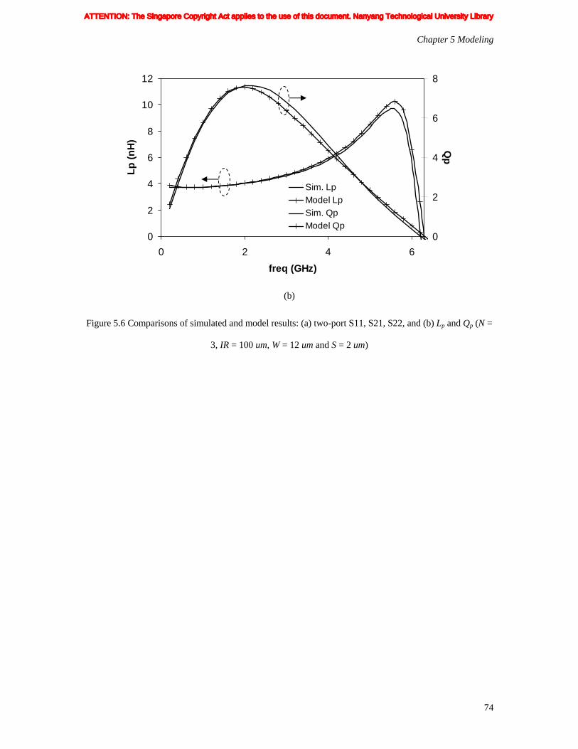
Chapter 5 Modeling
74
0
2
4
6
8
10
12
0 2 4 6freq (GHz)
Lp (n
H)
0
2
4
6
8
Qp
Sim. LpModel LpSim. QpModel Qp
(b)
Figure 5.6 Comparisons of simulated and model results: (a) two-port S11, S21, S22, and (b) Lp and Qp (N =
3, IR = 100 um, W = 12 um and S = 2 um)
ATTENTION: The Singapore Copyright Act applies to the use of this document. Nanyang Technological University Library
Chapter 6 Gilbert Cell Mixer with Transformer-Balun
75
Chapter 6 A 5 GHz Gilbert Cell Mixer with Transformer-Balun
On-chip transformers are used to perform coupling, biasing and filtering function in a CMOS Gilbert Cell
mixer. This chapter presents a 5 GHz, high isolation transformer based mixer using a 0.18um CMOS
process. The transformer works as an input balun to generate differential signals. A design procedure for
estimating the size of the transformer is illustrated. Resonant tuning is shown to reduce the losses between
input and output ports. The designed mixer has a voltage conversion gain of 12.4 dB, a third-order
intercept point of -1.2 dBm and a single-sideband noise figure of 13.1 dB. The excellent LO/RF and RF/IF
isolations are achieved up to 140.2 dB and 89.4 dB, respectively.
6.1 General Considerations
Mixers are essential building blocks of virtually every telecommunication system. They perform
frequency translation by multiplying two signals (and possibly their harmonics). Downconversion mixers
employed in the receive path have two distinctly different inputs, the RF port and the LO port. The signal
amplified by the LNA (and possibly filtered by an image-reject filter) is applied to the RF port. Thus, this
port must exhibit sufficiently low noise and high linearity. The latter because nearby interferers are
amplified by the LNA and hence can produce stronger intermodulation products.
Mixers can be passive or active. Passive mixers, where the transistors work in the linear region, typically
demonstrate conversion loss and excellent intermodulation performance at the expense of LO power. The
latter category, in the form of the well-known Gilbert cell, has prevailed in the majority of applications as
it entails advantages such as large conversion gain, high port-to-port isolation, and good noise
performance. It also requires lower LO power than the passive topology [48]. The disadvantage is
deterioration in linearity performance.
ATTENTION: The Singapore Copyright Act applies to the use of this document. Nanyang Technological University Library

Chapter 6 Gilbert Cell Mixer with Transformer-Balun
76
Conversion Gain: the gain of mixers can be defined in two ways. The “voltage conversion gain” is defined
as the ratio of the rms voltage of the IF signal to the rms voltage of the RF signal. These two signals are
centered at different frequencies. The “power conversion gain” of a mixer is defined as the IF power
delivered to the load divided by the available RF power from the source. If the input impedance and the
load impedance of the mixer are both equal to the source impedance, for example, 50 �, then the voltage
conversion gain and power conversion gain are equal when expressed in decibels.
SSB and DSB Noise Figures: for simplicity, a noiseless mixer with unity gain is considered. As shown in
Figure 6.1, the spectrum sensed by the RF port consists of a signal component and the thermal noise Rs in
both the signal band and the image band. Upon downconversion, the signal, the noise in the signal band,
and the noise in the image band are translated to wIF. Thus, the output SNR is half the input SNR if the
input frequency response of the mixer is the same for the signal band and the image band. In other words,
the noise figure of a noiselss mixer is equal to 3 dB. This refers to the “single-sideband” noise figure (SSB
NF) of the mixer. The term SSB indicates that the desired signal spectrum resides on only one side of the
LO frequency, a common case in heterodyne systems. If the input signal spectrum resides on the both
sides of wLO, the input and output SNR ratios are equal, giving a noise figure of 0 dB. This is called the
“double-sideband” noise figure (DSB NF). In summary, the SSB NF is 3 dB higher than the DSB NF if
the signal and image bands experience equal gains at the RF port of a mixer.
+
-Vin
Rs
wLO
X Y
Spectrum at X
Spectrum at Y
wLO
w
wIF
w
Signal band
Image bandThermal
Noise
wLO
w
wIF
w
Signal band
Image bandThermal
Noise
Figure 6.1 Folding of RF and image noise into the IF band [49]
ATTENTION: The Singapore Copyright Act applies to the use of this document. Nanyang Technological University Library
Chapter 6 Gilbert Cell Mixer with Transformer-Balun
77
Port-to-Port Isolation: the isolation between each two ports of a mixer is critical. The LO-RF feedthrough
results in LO leakage to the LNA and eventually the antenna, whereas the RF-LO feedthrough allows
strong interferers in the RF path to interact with the local oscillator driving the mixer. The LO-IF
feedthrough is important because if substantial LO signal exists at the IF output even after low-pass
filtering, then the following stage may be desensitilized. Finally, the RF-IF isolation determines what
fraction of the signal in the RF path directly appears in the IF, a critical issue with respect to the even-
order distortion problem in homodyne receivers [49].
6.2 Transformer Design
As mentioned in Chapter 1, on-chip transformers have found extensive applications in RF designs such as
impedance transformation/matching, signal coupling, balun implementation. In the case of balun
application, the balanced structure is often applied and circuits need a balun to generate differential
signals. The frequency response of circuits is enhanced along with the advancement in technologies The
balun is integrated into RFICs to eliminate the mismatch of the external baluns and cables. Thus the useful
bandwidth could be extended. Baluns, such as Marchand baluns [50], phase inverter rat-race couplers [51],
transformes [52], etc, function as a single-to-differential converter with a broadband property and they are
widely used. However, microwave balun structures require physical dimensions on the order of the signal
wavelength. These devices consume too much chip area when operating below approximately 15 GHz
[52]. Compared with baluns, transformers have smaller size and higher operation bandwidth ratio [53]. It
can operate with low supply voltage since there is no dc voltage drop on the transformer. Besides, the
transformer is a linear device.
The goal of this design procedure is to estimate the optimized geometry of a transformer balun working at
the desired center frequency, with the lowest possible losses and consuming as little chip area as possible.
ATTENTION: The Singapore Copyright Act applies to the use of this document. Nanyang Technological University Library

Chapter 6 Gilbert Cell Mixer with Transformer-Balun
78
N affects the transformer’s performance mostly. As N increases, larger area occupied by the transformer
causes an increase in the substrate capacitance and turn-to-turn capacitive coupling, thereby decreasing fres.
On the other hand, more turns induces stronger magnetic coupling. As a result, Gmax increases. Usually N
is chosen to be 3 or 4 to ensure the large working frequency range and good Gmax. Since the mixer
designed works at 5 GHz, N = 3 is chosen to ensure fres is high enough (beyond 13 GHz).
Similar to the case of N, fres drops as IR (or W) increases. However, the negative magnetic coupling also
drops, since the coils carrying opposite currents become further apart. Thus, |S21| increases (see Figure
6.2). The transformer K-factor improves as W decreases at high operating frequencies. This is because the
proximity effect pushes the ac current towards the inner turn of the transformer, making the negative
mutual coupling stronger. S determines the positive mutual inductance between conductors. Narrower
track spacing improves the magnetic coupling between the primary and secondary conductors, which
increases in K. But W and S should not be kept minimum allowable for the technology. Small W increases
the resistive loss of conductors and small S promotes stronger turn-to-turn capacitive coupling. In this
design example, they are chosen to be 6 um and 2 um.
The transformer designed has the following properties: the primary inductance Lp = 2.08 nH, the
secondary inductance Ls = 1.78 nH, Qpmax = 7.8, Qsmax = 7 at fQmax = 5 GHz, and the coupling factor K =
0.81.
The phase of the voltage induced at the secondary of the transformer depends on the choice of the
reference terminal. Figure 6.3 compares |S21| with the inverting and non-inverting connections. In the
inverting connection, port 2 is connected to the load and port 4 is grounded for an ac signal source with
the output and ground applied between port 1 and port 3. Thus, the secondary output is antiphase to the
signal applied to the primary. In the non-inverting connection, port 4 is connected to the load with port 2
grounded. The magnitude responses of two connections are different as frequency increases. This is due to
the interwinding capacitance, which induces a zero in the response of the non-inverting transformer so that
ATTENTION: The Singapore Copyright Act applies to the use of this document. Nanyang Technological University Library

Chapter 6 Gilbert Cell Mixer with Transformer-Balun
79
the transformer secondary has a bandpass response [53]. The phase difference between inverting and non-
inverting connections is 180 degrees at frequencies below 7.5 GHz, which defines the upper edge of the
transformer’s operating band. Table 7 presents the values of circuit elements at primary side for the
transformer designed through curve-fitting technique.
Figure 6.2 |S21| (dB) versus frequency for varying IR
Figure 6.3 Comparison of inverting and non-inverting S21 of a 3-turn transformer
ATTENTION: The Singapore Copyright Act applies to the use of this document. Nanyang Technological University Library

Chapter 6 Gilbert Cell Mixer with Transformer-Balun
80
6.3 Circuit Design
Figure 6.4 illustrates the Gilbert Cell Mixer topology. It consists of an on-chip transformer as input balun
and two levels of transistors. There are several advantages to use the transformer at the input: (1) There
are no restrictions to the external dc potential at the input terminals; (2) No external input dc blocking
capacitor is required; (3) The input signal can be applied differentially or single-ended if one input port is
grounded [54]. The passive transformer introduces virtually no distortion to the RF signal, thereby
preserving the linearity. Moreover, the input node is made resonate at 5 GHz by adding one more
capacitor in parallel with the secondary winding of the transformer. By resonating the input, the
substantial losses that arise from imperfect magnetic coupling between two windings of a transformer is
reduced, thereby improving the conversion gain of the circuit. Two LO ports are driven by a differential
voltage.
Figure 6.4 Gilbert cell mixer topology
ATTENTION: The Singapore Copyright Act applies to the use of this document. Nanyang Technological University Library

Chapter 6 Gilbert Cell Mixer with Transformer-Balun
81
The following figures display the performance of the final mixer circuit. Figure 6.5 represents the voltage
conversion gain of the mixer when sweeping RF- and LO-input frequency under 6 dBm LO power. The
conversion gain is larger than 12 dB within a 10 MHz IF bandwidth. The 1-dB input compression point is
around -11 dBm. In Figure 6.6, the third-order intermodulation distortion in terms of amplitude difference
of first- and third-order products (IM3) of a two tone test is depicted. With the two RF tones set to 4.7999
GHz and 5.0001 GHz, the IIP3 is found to be around -1.2 dBm. Figure 6.7 shows the characteristics of
port to port isolations. It is obvious that the mixer designed has excellent isolations of 140.2 dB and 89.4
dB among LO/RF and RF/IF ports, respectively. In addition, the SSB noise figure of the mixer is about
13.1 dB (see Figure 6.8). The trade-offs among noise, nonlinearity, and power dissipation typically lead to
a compromise in the design. The overall mixer design occupies 0.06 mm2, of which 0.04 mm2 is the
effective area for the physical implementation of the transformer. Figure 6.9 display the core layout of the
mixer circuit including the transformer. Table 9 summarizes the overall performance.
9
10
11
12
13
14
15
5.0E+09 5.2E+09 5.4E+09 5.6E+09 5.8E+09 6.0E+09
RF Frequency (Hz)
Con
vers
ion
Gai
n (d
B)
Figure 6.5 Conversion Gain vs RF frequency
ATTENTION: The Singapore Copyright Act applies to the use of this document. Nanyang Technological University Library

Chapter 6 Gilbert Cell Mixer with Transformer-Balun
82
-100
-80
-60
-40
-20
0
20
-60 -50 -40 -30 -20 -10 0 10 20RF Input Power (dB)
IF O
uput
Pow
er (d
B)
third orderfundamental
Figure 6.6 Mixer two tone test
60
80
100
120
140
160
4.0E+09 4.5E+09 5.0E+09 5.5E+09 6.0E+09RF freq
LO/R
F &
RF/
IF Is
olat
ions
(dB
)
LO to RF IsolationRF to IF Isolation
Figure 6.7 Isolations of LO to RF and RF to IF vs RF frequency
0
5
10
15
20
25
4.0E+09 4.5E+09 5.0E+09 5.5E+09 6.0E+09RF Frequency (Hz)
NF
(dB
)
Figure 6.8 SSB Noise Figure vs RF frequency
ATTENTION: The Singapore Copyright Act applies to the use of this document. Nanyang Technological University Library

Chapter 6 Gilbert Cell Mixer with Transformer-Balun
83
Figure 6.9 Core layout of the transformer-based mixer including the transformer
ATTENTION: The Singapore Copyright Act applies to the use of this document. Nanyang Technological University Library
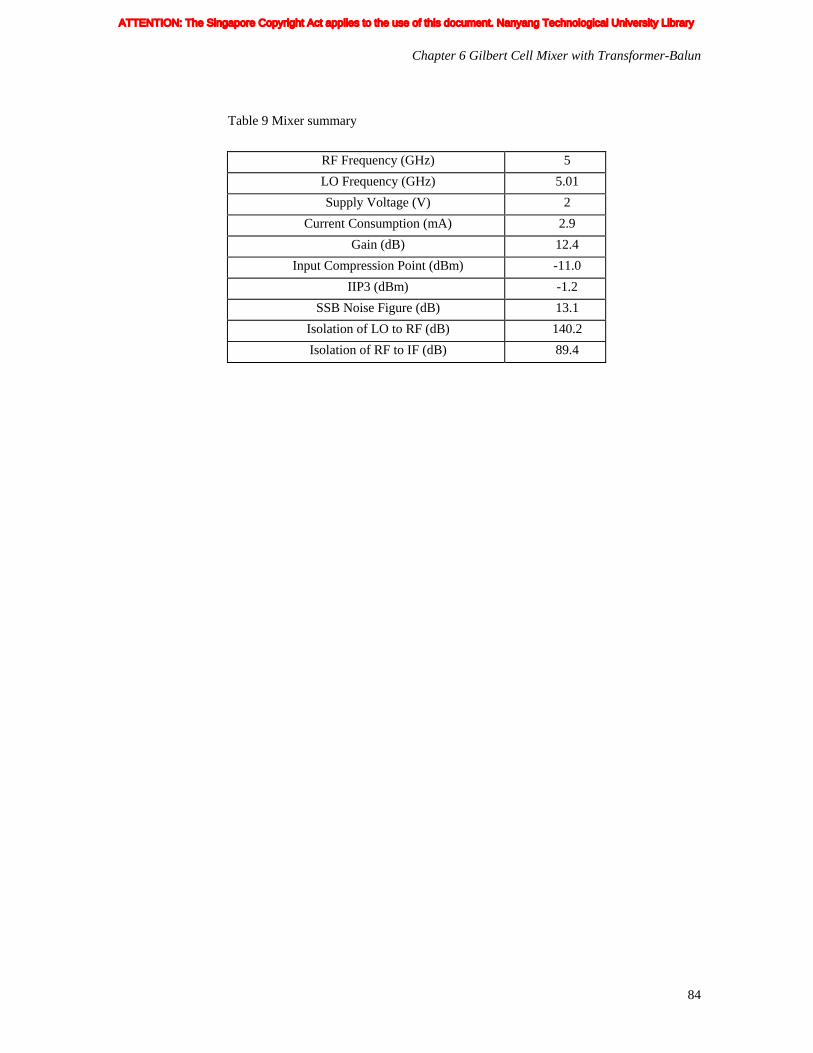
Chapter 6 Gilbert Cell Mixer with Transformer-Balun
84
Table 9 Mixer summary
RF Frequency (GHz) 5
LO Frequency (GHz) 5.01
Supply Voltage (V) 2
Current Consumption (mA) 2.9
Gain (dB) 12.4
Input Compression Point (dBm) -11.0
IIP3 (dBm) -1.2
SSB Noise Figure (dB) 13.1
Isolation of LO to RF (dB) 140.2
Isolation of RF to IF (dB) 89.4
ATTENTION: The Singapore Copyright Act applies to the use of this document. Nanyang Technological University Library
Chapter 7 Conclusions and Recommendations
85
Chapter 7 Conclusions and Recommendations
7.1 Conclusions
The rapid growth of modern wireless communication market has caused soaring demands for low cost RF
products. Among all established technologies, due to its low fabrication cost as well as high packaging
density, silicon technology has been recognized as one of the most promising technologies to satisfy the
requirement of rapid expanding wireless market.
The one-chip transformer is one of the key elements in monolithic RFIC designs such as low-noise
amplifiers (LNAs), voltage-controlled oscillators (VCOs), mixers, passive element filters, impedance
matching networks, etc. As such, there are great incentives in designing, optimizing, modeling and
miniaturizing on-chip transformers. Despite efforts put in by many researchers, achieving an accurate
model of the transformer still remains a challenge due to the complexity of capacitive and magnetic losses
related to the semiconducting substrate. All these have served as the key motivations for this project.
In this report, one common configuration of on-chip transformers, the planar interleaved transformer has
been studied. As most of the works carried out in this project utilized full-wave 3D electromagnetic (EM)
simulations, an overview of the simulator (Ansoft HFSS) has been provided with its advantages and
disadvantages illustrated. The simulator’s validity to predict inductor’s performance has been verified by
comparing the simulation results obtained from HFSS and the corresponding measured data. Then the
geometrical parameters of the transformer, such as the number of turns (N), inner radius (IR), track width
(W), and turn-to-turn spacing (S) were varied to find the optimized geometry and study the resultant
changes on the transformer’s performance, in terms of the quality factor Q, self-inductance L, the coupling
factor K, the maximum available gain Gmax and the resonant frequency fres. Various loss mechanisms
ATTENTION: The Singapore Copyright Act applies to the use of this document. Nanyang Technological University Library

Chapter 7 Conclusions and Recommendations
86
pertaining to the transformer were also understood and its associated lumped equivalent–circuit model was
developed. The skin effect, parasitic capacitive coupling between the windings, and coupling between the
input and output ports are carefully examined by the proposed model. Moreover, this model is scalable
over a wide range of layout dimensions (N > 1). A set of analytical equations can be used to calculate all
the circuit elements.
The conclusion of the simulation results can be used to provide useful on-chip transformer design
guidelines. A design with 3 to 4 turns is optimum, as larger N will degrade fres, while smaller N can not
achieve higher inductance values. IR of the transformer should not be larger than 100 um, otherwise it will
increase the substrate parasitics and degrade the transformer’s performance. For the same reason, the
metal width W of 10-15 um is close to the optimum for transformer designs with N = 3 and S = 2 um. In
addition, using the closet spacing S between lines that is allowed by the technology will give a larger K
value, which is due to stronger magnetic coupling between adjacent metal lines.
The model proposed for the interleaved transformer is a combination of two on-chip inductors’ models. In
this model, additional ladder circuit is used to capture the strong skin effect at higher frequencies. And
seven parasitic capacitances are placed between different ports to model the cross coupling effect. Based
on the simulation results, the curve-fitting techniques were used to find these capacitances’ values and the
coupling factor K.
On-chip transformers are used to perform coupling, biasing and filtering function in a CMOS Gilbert Cell
mixer. This report also presents a 5 GHz, high isolation transformer based mixer using a 0.18um CMOS
process. The transformer works as an input balun to generate differential signals. A design procedure for
estimating the size of the transformer is illustrated. Resonant tuning is shown to reduce the losses between
input and output ports. The designed mixer has a voltage conversion gain of 12.4 dB, a third-order
intercept point of -1.2 dBm and a single-sideband noise figure of 13.1 dB. The excellent LO/RF and RF/IF
isolations are achieved up to 140.2 dB and 89.4 dB, respectively.
ATTENTION: The Singapore Copyright Act applies to the use of this document. Nanyang Technological University Library

Chapter 7 Conclusions and Recommendations
87
7.2 Recommendations
A few interesting ideas for further research are suggested in this section.
1) More accurate lumped-equivalent model can be developed for the interleaved transformer. A good S-
parameter fit has been achieved in this project. The errors are only a few percent. However, there is still
room to improve the accuracy of the equivalent lumped-element parameters. The formula to calculate the
inter-winding capacitances is quite complicated. Further simplification without loss of accuracy is needed.
Moreover, it could be helpful to fabricate more on-chip transformers to obtain the measured results. Thus
the validation of the models can be further demonstrated.
2) Stacked transformers, which provide better area-efficiency, higher self-inductance values and coupling
efficiency compared to the interleaved transformer, can be studied. Further more, a combination of
stacked and interleaved transformers may also be explored.
3) In order to help circuit designers to quickly find the transformer design they are interested, a search
tool, can be developed. It allows users to search for different transformer designs based on our simulation
results. The user can either search by defining the physical dimensions (N, IR, W, and S) or the electrical
performance of the transformer (L, Q, and K).
4) The transformer design is very application dependent. Other transformer applications can be tried to test
the capability of the transformer designed. For example, the passive mixer can be combined with the
transformer-balun to save the power consumption.
ATTENTION: The Singapore Copyright Act applies to the use of this document. Nanyang Technological University Library

References
88
References
1. N. Camilleri et.al, “New develop trends for silicon RF device technologies,” IEEE Microwave and
Millimeter-Wave Monolithic Circuits Symp., pp. 5-8, May 1994.
2. P.R. Gray and R.G. Meyer, “Future directions in silicon ICs for RF personal communications,” Proc.
IEEE 1995 Custom Integrated Circuits Conference, pp. 83-90, May 1995.
3. S.S. Mohan, “The design, modeling and optimization of on-chip inductor and transformer circuits”,
PhD thesis, Stanford University, Dec. 1999.
4. J. R. Long and M. A. Copeland, “A l.9GHz low-voltage silicon bipolar receiver front-end for wireless
personal communications systems,” IEEE J. Solid-State Circuits, vol. 30, no.12, pp. 1438–1448, Dec.
1995.
5. D. Ferguson, P. Bauhahn, J. Keuper, R. Lokken, J. Culp, C. Chao, and A. Podell, “Transformer coupled
high-density circuit technique for MMIC,” IEEE MTT-S Dig.,vol. 84, # 001, pp. 34–36, May 1984.
6. S. A. Jamison, A. Podell, M. Helix, P. Ng, and C. Chao, “Inductively coupled push–pull amplifiers for
low cost monolithic microwave IC’s,” IEEE GaAs IC Symp., pp. 91–93, Oct. 1982.
7. L. Selmi and B. Ricco, “Design of an X-band transformer-coupled amplifier with improved stability
and layout,” IEEE J. Solid-State Circuits, vol. 28, no. 6, pp. 701–703, Jun. 1993.
8. Jianjun J. Zhou and David J. Allstot, “Monolithic transformers and their application in a differential
CMOS RF low-noise amplifier”, IEEE J. Solid-State Circuits, vol. 33, no. 12, pp. 2020-2027, Dec. 1998.
ATTENTION: The Singapore Copyright Act applies to the use of this document. Nanyang Technological University Library
References
89
9. S.S. Mohan, and T.H. Lee, “Modeling and characterization of on-chip transformers”, Proc IEEE Int
Electron Devices Mtg, San Francisco, CA, pp. 531–534, Dec. 1998.
10. A.M. Niknejad and R.G. Meyer, “Analysis, design and optimization of spiral inductors and
transformers for SiRF IC’s”, IEEE J. Solid-State Circuits, vol. 33, no. 10, pp. 1470– 148, Oct. 1998.
11. D. Kehrer, “Characterization of integrated lumped inductors and transformers”, Ronald Thüringer,
9326356, Pretschgasse 21, 1110 Wien, Apr. 2002.
12. W. Gao, C. Jiao and T. Liu, “Scalable compact circuit model for differential spiral transformers in
CMOS RFICs,” IEEE Trans. Electron Devices. vol. 53, no. 9, pp. 2187-2194, Sep. 2006.
13. O. E.-Gharniti, E. Kerherve, and J.-B. Bergueret, “Modeling and characterization of on-chip
transformers for silicon RFIC,” IEEE Trans. Microw. Theory Tech., vol. 55, no. 4, pp. 607–615, Apr.
2007.
14. “Ansoft HFSS User’s Manual”, Ansoft HFSS software, Jan. 2001.
15. Shu-Jun Pan, Wen-Yan Yin and Le-Wei Li, “Comparative investigation on various on-chip center-
tapped interleaved transformers”, Wiley Periodicals, Inc. Int. J RF and Microwave CAE 14, pp. 424-432,
Dec. 2003.
16. A. Zolfaghari, A. Chan, and B. Razavi, “Stacked inductors and transformers in CMOS technology,”
IEEE J. Solid-State Circuits, vol. 36, no. 4, pp. 620–628, Apr. 2001.
17. V. Shwetabh and M.C. Jose, “On-chip inductors and transformers,” Sun Microsystems, CA 94303–
4900, Dec. 1999.
ATTENTION: The Singapore Copyright Act applies to the use of this document. Nanyang Technological University Library

References
90
18. T. H. Lee, “The Design of CMOS Radio-Frequency Integrated Circuits,” Cambridge University Press,
Cambridge, 1998.
19. H. M. Greenhouse, “Design of planar rectangular microelectronic inductors,” IEEE Trans. Parts,
Hybrids, Packag., vol. PHP-10, no. 2, pp. 101–109, Jun. 1974.
20. R. L. Bunch, D. I. Sanderson, S. Raman, “Quality factor and inductance in differential IC
implementations,” IEEE Microwave Magazine, vol. 3, no. 2, pp. 82-92, Jun. 2002.
21. Lim, Suh Fei, “Optimization and modeling of on-chip inductor”, T3, Master thesis, Nanyang
Technogical University, May 2004.
22. J. N. Burghartz, M. Soyuer, and K. A. Jenkins, “Microwave inductors and capacitors in standard
multilevel interconnect silicon techonology,” IEEE Trans. Microwave Theory Tech., vol. 44, no. 1, pp.
100-104, Jan. 1996.
23. J. Y. -C. Chang, A. A. Abidi, and M. Gaitan, “Large suspend inductors and silicon and their use in a 2-
um CMOS RF amplifier,” IEEE Electron Device Lett., vol. 14, no. 5, pp. 246-248, May 1993.
24. Y. Cao et al., “Frequency-independent equivalent-circuit model for on-chip spiral inductors,” IEEE J.
Solid-State Circuits, vol. 38, no. 3, pp. 419 – 426, Mar. 2003.
25. W. Gao, C. Jiao and T. Liu, “Scalable compact circuit model for differential spiral transformers in
CMOS RFICs,” IEEE Trans. Electron Devices. vol. 53, no. 9, p. 2187-2194, Sep. 2006.
26. F. W. Grover, Inductance Calculations. New York: Dover, 1962.
ATTENTION: The Singapore Copyright Act applies to the use of this document. Nanyang Technological University Library

References
91
27. H. M. Greenhouse, “Design of planar rectangular microelectronic inductors,” IEEE Trans. Parts,
Hybrids, Packag., vol. PHP-10, no. 2, pp. 101–109, Jun. 1974.
28. C. P. Yue and S. S. Wong, “Physical modeling of spiral inductors on silicon,” IEEE Trans. Electron
Devices, vol. 47, no. 3, pp. 560-568, Mar 2000.
29. F. M. Rotella, V. Blaschke, and D. Howard, “A broad-band scalable lumped-element inductor model
using analytic expressions to incorporate skin effect, substrate loss, and proximity effect,” in IEDM Tech.
Dig., pp. 471–474, Dec. 2002.
30. S. Jenei, B. K. J. C. Nauwelaers, and S. Decoutere, “Physical-based close-form inductance expression
for compact modeling of integrated spiral inductors,” IEEE J. Solid-State Circuits, vol. 37, no. 1, pp. 77–
80, Jan. 2002.
31. J. Crols, P. Kinget, J. Cranninckx, and M. Steyaert, “An analytic model of planar inductors on lowly
doped silicon substrate for high frequency analog design up to 3 GHz,” in VLSI Symp. Tech. Dig., pp. 28–
29, Jun. 1996.
32. J. R. Long, and M. A. Copeland, “The modeling, characterization, and design of monolithic inductors
for silicon RF IC’s,” IEEE J. Solid-State Circuits, vol. 32, no. 3, Mar. 1997.
33. X. Huo et al., “ A physical model for on-chip spiral inductors with accurate substrate modeling,” IEEE
Trans. Electron Devices, vol. 53, no. 12, pp. 2942-2949, Dec. 2006.
34. M. T. Ahmed, et al., “Skin and proximity effect calculation using method of fundamental solutions,"
IEEE Trans. Magnetics, vol. 24, pp. 2667-2669, Nov. 1998.
ATTENTION: The Singapore Copyright Act applies to the use of this document. Nanyang Technological University Library

References
92
35. W. B. Kuhn and N. M. Ibrahim, “Analysis of current crowding effects in multiturn spiral inductors,”
IEEE Trans. Microwave Theory Tech., vol.49, no. 1, pp. 31–38, Jan. 2001.
36. T. Biondi, A. Scuderi, E. Ragonese, and G. Palmisano, “Analysis and modeling of layout scaling in
silicon integrated stacked transformers,” IEEE Trans. Microw. Theory Tech., vol. 54, no. 5, pp. 2203–
2210, May 2006.
37. J. Sieiro, et al., “A physical frequency-dependent compact model for RF integrated inductors," IEEE
Trans. Microwave Theory and Techniques, vol. 50, pp. 384-392, Jan. 2002.
38. I. Aoki, S.D. Kee, D.B. Rutledge and A. Hajimiri, “Distributed active transformer-a new power-
combining and impedance-transformation technique”, IEEE Trans Microwave Theory Tech, vol. 50, no. 1,
pp. 316–331, Jan. 2002.
39. Rotella et al., “Characterization, design, modeling and model validation of silicon on-wafer M:N balun
components under matched and unmatched conditions,” J. Solid-State Circuits, vol. 41, no. 5, pp. 1201-
1209, May 2006.
40. E. Pettenpaul, H. Kapusta, A. Weisgerber, H. Mampe, J. Luginsland, and I. Wolff, “CAD models of
lumped elements on GaAs up to 18 GHz,” IEEE Trans. Microwave Theory Tech., vol. MTT-36, pp. 294–
304, Feb. 1988.
41. S. S. Mohan et al., “Simple accurate expressions for planar spiral inductances,” IEEE J. Solid-State
Circuits, vol. 34, no. 10, pp. 1419–1424, Oct. 1999.
42. E. B. Rosa, “Calculation of the self-inductances of single-layer coils,” Bull. Bureau Standards, vol. 2,
no. 2, pp. 161-187, 1906.
ATTENTION: The Singapore Copyright Act applies to the use of this document. Nanyang Technological University Library

References
93
43. J. C. Maxwell, A treatise on electricity and magnetism, 3rd ed. New York: Dover, 1967.
44. S. Kim and D. P. Neikirk, “Compact equivalent circuit model for the skin effect,” in IEEE Trans.
Microwave Theory and Techniques Symp. Dig., vol. 3, #17-21, pp. 1815–1818, Jun. 1996.
45. W. Gao, and Z. P. Yu, “Scalable compact circuit model and synthesis for RF CMOS spiral inductors,”
IEEE Trans. Microwave Theory and Techniques Symp. vol. 54, no. 3, p. 1055-1064, Mar. 2006.
46. N. Van der Meijs and J. T. Fokkema, “VLSI circuit reconstruction from mask topology,” Integration,
vol. 2, No. 2, pp. 85–119, Mar. 1984.
47. W. Heinrich, “Quasi-TEM description of MMIC coplanar lines including conductor-loss effects,”
IEEE Trans. Microw. Theory Tech., vol. 41, no. 1, pp. 45–52, Jan. 1993.
48. P. J. Sullivan, B. A. Xavier and W. H. Ku, “Low voltage performance of a microwave CMOS Gilbert
cell mixer,” IEEE J. Solid-State Circuits, vol. 32, no. 7, pp. 1151-1155, Jul. 1997.
49. Behzad Razavi, RF microelectronics, Prentice Hall PTR, pp. 182-186, 1997.
50. K. S. Ang and I. D. Robertson, "Analysis and design of impedance-transforming planar Marchand
baluns," IEEE Trans. Microw. Theory Tech., vol. 49, no. 2, pp. 402-406, Feb. 2001.
51. T. Wang and K. Wu, "Size-reduction and band-broadening design technique of uniplanar hybrid ring
coupler using phase inverter for M(H)MIC's," IEEE Trans. Microw. Theory Tech., vol. 47, no. 2, pp. 198-
206, Feb. 1999.
ATTENTION: The Singapore Copyright Act applies to the use of this document. Nanyang Technological University Library

References
94
52. J. R. Long, “Monolithic transformers for silicon RF IC design,” IEEE J. Solid-State Circuits, vol. 35,
no. 9, pp. 1368-1382, Sep. 2000.
53. S. C. Tseng, C. C. Meng, C. K. Wu, and G. W. Guang, “Low-voltage GaInp/GaAs HBT wideband
Gilbert downconverter using transformer RF balun,” IEEE. Microw. Symp. Dig., pp. 2149-2152, Jun.
2007.
54. W. Simbürger, H-D. Wohlmuth, P. Weger, and A. Heinz, “A monolithic transformer coupled 5-W
silicon power amplifier with 59% PAE at 0.9GHz,” IEEE J. Solid-State Circuits, vol. 34, p. 1881-1892,
Dec. 1999.
ATTENTION: The Singapore Copyright Act applies to the use of this document. Nanyang Technological University Library

Author’s publications
95
Author’s Publications
Journal Publications
D. Zhao, K. S. Yeo, M. A. Do, C. C. Boon, “Characterization, design and modeling of on-chip interleaved
transformers in CMOS RFICs”, 2nd submission to IET Circuits, Devices and System, 2008.
D. Zhao, K. S. Yeo, M. A. Do, C. C. Boon, “A 5GHz Gilbert cell mixer with on-chip transformer-balun”,
submitted to IET Microwave Antennas & Propagation, 2008.
ATTENTION: The Singapore Copyright Act applies to the use of this document. Nanyang Technological University Library
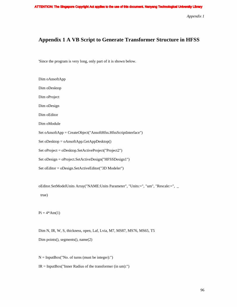
Appendix 1
96
Appendix 1 A VB Script to Generate Transformer Structure in HFSS
'Since the program is very long, only part of it is shown below.
Dim oAnsoftApp
Dim oDesktop
Dim oProject
Dim oDesign
Dim oEditor
Dim oModule
Set oAnsoftApp = CreateObject("AnsoftHfss.HfssScriptInterface")
Set oDesktop = oAnsoftApp.GetAppDesktop()
Set oProject = oDesktop.SetActiveProject("Project2")
Set oDesign = oProject.SetActiveDesign("HFSSDesign1")
Set oEditor = oDesign.SetActiveEditor("3D Modeler")
oEditor.SetModelUnits Array("NAME:Units Parameter", "Units:=", "um", "Rescale:=", _
true)
Pi = 4*Atn(1)
Dim N, IR, W, S, thickness, open, Laf, Lvia, M7, MS87, MS76, MS65, T5
Dim points(), segments(), name(2)
N = InputBox("No. of turns (must be integer):")
IR = InputBox("Inner Radius of the transformer (in um):")
ATTENTION: The Singapore Copyright Act applies to the use of this document. Nanyang Technological University Library

Appendix 1
97
W = InputBox("Metal Width of the conductor (in um):")
S = InputBox("Turn to turn spacing (in um):")
Laf=6
open=9.5
Lvia=3
thickness=2
MS87=-0.9
MS76=-0.9
T6=-0.54
T7=-0.54
MS65=-0.54
T5=-0.9
T_SiN=0.3
T_ILD=-8.05
T_Si=-150
T_HDP=3.1
name(1)="_upper"
name(2)="_lower"
'---------------------------------------------------------------------------------
For i=1 to N
m=1
length=2*(IR+(i-1)*2*(W+S))*tan(Pi/8)
mean=length*cos(Pi/4)
x1=(IR+(i-1)*2*(W+S))
ATTENTION: The Singapore Copyright Act applies to the use of this document. Nanyang Technological University Library

Appendix 1
98
y1=(open+Laf-Lvia)
y2=x1*tan(Pi/8)
x3=(x1-mean)
y3=x1
x4=(x3-length)
x5=(x4-mean)
oEditor.CreatePolyline Array("NAME:PolylineParameters", "CoordinateSystemID:=", -1,
"IsPolylineCovered:=", true, "IsPolylineClosed:=", false, Array("NAME:PolylinePoints",
Array("NAME:PLPoint", "X:=", cstr(x1)+"um", "Y:=", cstr(y1)+"um", "Z:=", "0"),
Array("NAME:PLPoint", "X:=", cstr(x1)+"um", "Y:=", cstr(y2)+"um", "Z:=", "0"),
Array("NAME:PLPoint", "X:=", cstr(x3)+"um", "Y:=", cstr(y3)+"um", "Z:=", "0"),
Array("NAME:PLPoint", "X:=", cstr(x4)+"um", "Y:=", cstr(y3)+"um", "Z:=", "0"),
Array("NAME:PLPoint", "X:=", cstr(x5)+"um", "Y:=", cstr(y2)+"um", "Z:=", "0"),
Array("NAME:PLPoint", "X:=", cstr(x5)+"um", "Y:=", cstr(y1)+"um", "Z:=", "0")),
Array("NAME:PolylineSegments", Array("NAME:PLSegment", "SegmentType:=", _
"Line", "StartIndex:=", 0, "NoOfPoints:=", 2), Array("NAME:PLSegment", "SegmentType:=", _
"Line", "StartIndex:=", 1, "NoOfPoints:=", 2), Array("NAME:PLSegment", "SegmentType:=", _
"Line", "StartIndex:=", 2, "NoOfPoints:=", 2), Array("NAME:PLSegment", "SegmentType:=", _
"Line", "StartIndex:=", 3, "NoOfPoints:=", 2), Array("NAME:PLSegment", "SegmentType:=", _
"Line", "StartIndex:=", 4, "NoOfPoints:=", 2))), Array("NAME:Attributes", "Name:=", _
"S_Polyline"+cstr(i)+name(m), "Flags:=", "", "Color:=", "(132 132 193)", "Transparency:=", 0,
"PartCoordinateSystem:=", "Global", "MaterialName:=", "vacuum", "SolveInside:=", true)
oEditor.CreateRectangle Array("NAME:RectangleParameters", "CoordinateSystemID:=", _
-1, "IsCovered:=", true, "XStart:=", cstr(x1)+"um", "YStart:=", cstr(y1)+"um", "ZStart:=", _
ATTENTION: The Singapore Copyright Act applies to the use of this document. Nanyang Technological University Library

Appendix 1
99
"0", "Width:=", cstr(thickness)+"um", "Height:=", cstr(W)+"um", "WhichAxis:=", "y"),
Array("NAME:Attributes", "Name:=", "Rectangle"+cstr(i)+name(m), "Flags:=", "", "Color:=", "(132 132
193)", "Transparency:=", 0, "PartCoordinateSystem:=", "Global", "MaterialName:=", "vacuum",
"SolveInside:=", true)
oEditor.SweepAlongPath Array("NAME:Selections", "Selections:=", _
"S_Polyline"+cstr(i)+name(m)+","+"Rectangle"+cstr(i)+name(m)),
Array("NAME:PathSweepParameters", "CoordinateSystemID:=", -1, "DraftAngle:=", "0deg",
"DraftType:=", "Extended", "CheckFaceFaceIntersection:=", false, "TwistAngle:=", "0deg")
oEditor.ChangeProperty Array("NAME:AllTabs", Array("NAME:Geometry3DAttributeTab",
Array("NAME:PropServers", "Rectangle"+cstr(i)+name(m)), Array("NAME:ChangedProps",
Array("NAME:Name", "Value:=", "S"+cstr(i)+name(m)))))
oEditor.DuplicateMirror Array("NAME:Selections", "Selections:=", "S"+cstr(i)+name(m)),
Array("NAME:DuplicateToMirrorParameters", "DuplicateMirrorBaseX:=", "0um",
"DuplicateMirrorBaseY:=", "0um", "DuplicateMirrorBaseZ:=", "0um", "DuplicateMirrorNormalX:=", _
"0um", "DuplicateMirrorNormalY:=", "-30um", "DuplicateMirrorNormalZ:=", "0um"),
Array("NAME:Options", "DuplicateBoundaries:=", false)
oEditor.ChangeProperty Array("NAME:AllTabs", Array("NAME:Geometry3DAttributeTab",
Array("NAME:PropServers", "S"+cstr(i)+name(1)+"_1"), Array("NAME:ChangedProps",
Array("NAME:Name", "Value:=", "S"+cstr(i)+name(2)))))
next
for i=1 to N step 2
…
ATTENTION: The Singapore Copyright Act applies to the use of this document. Nanyang Technological University Library

Appendix 2
100
Appendix 2 Geometrical Mean Length (LGML) Calculation
The LGML of primary/secondary winding is calculated by approximating the octagonal structure as circular
shapes.
Figure 2 Secondary winding of the interleaved transformer: (a) octagonal, and (b) circular
Take the secondary winding as an example. Total length is the sum of each individual turn’s length.
)]22
)(1[(2...)22
(2)22
(2,
wdNSw
wdwdL ininin
SGML +−⋅+++++⋅++⋅= πππ
)](2
)1()
22([2 Sw
NNwdN in +
−++⋅= π
][ 22 NSNwSNwNNwdN in −−+++⋅⋅= π
])1([ 2wNSNNdN in +−+⋅⋅= π
It should be noted that here S = W + 2S, as we are considering the interleaved transformer and S is the
spacing between primary and secondary winding. Therefore,
ATTENTION: The Singapore Copyright Act applies to the use of this document. Nanyang Technological University Library

Appendix 2
101
])2)(1([ 2, wNswNNdNL inSGML ++−+⋅⋅= π
Similarly, for the primary winding,
])2)(1()([ 2, wNswNNswdNL inPGML ++−+++⋅⋅= π
ATTENTION: The Singapore Copyright Act applies to the use of this document. Nanyang Technological University Library