Embed Size (px)
Citation preview
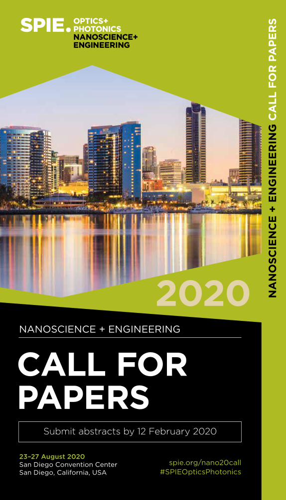
CALL FORPAPERS
Submit abstracts by 12 February 2020
NA
NO
SCIE
NC
E +
EN
GIN
EE
RIN
G C
ALL
FO
R P
AP
ER
S
NANOSCIENCE + ENGINEERING
2020
23–27 August 2020San Diego Convention CenterSan Diego, California, USA
spie.org/nano20call#SPIEOpticsPhotonics

- Present to experts
- Publish your results internationally
- Gain experience in scientific communication
- Connect with researchers from other disciplines
- See where your work fits into global optics and photonics research
Present your workNanoscience + EngineeringNanotechnology and quantum science are creating applications in such diverse fields as energy, information storage, and computing. Prepare to present your work in metamaterials, nanophotonic materials, plasmonics, quantum materials and devices, optical trapping, spintronics, nanostructured devices, nanoengineering, nanoimaging, nanospectroscopy, low-dimensional materials, and artificial intelligence.
spie.org/nano20call
Conferences and Courses23–27 August 2020
Exhibition 25–27 August 2020
San Diego Convention Center, San Diego, California, USA
New data laws are in effectUnless you opt in to receive email from us,
you will not receive any SPIE info about SPIE Optics + Photonics.
spie.org/signup

Tel: +1 360 676 3290 • [email protected] • #SPIEOpticsPhotonics 1
PB SPIE OPTICS+PHOTONICS 2020 • spie.org/nano20call
Submit abstracts by 12 February 2020
TechnologiesExplore these technical areas to find the right conference to submit your research.
Nanoscience• Metamaterials, Metadevices, and Metasystems
• Active Photonic Platforms
• Plasmonics: Design, Materials, Fabrication, Characterization, and Applications
• Optical Trapping and Optical
• Physical Chemistry of Semiconductor Materials and Interfaces
• Low-Dimensional Materials and Devices
• UV and Higher Energy Photonics: From Materials to Applications
• Nanoengineering: Fabrication, Properties, Optics, Thin Films, and Devices
• Enhanced Spectroscopies and Nanoimaging - NEW
• Emerging Topics in Artificial Intelligence 2020 - NEW
Quantum Sciences and Technology• Spintronics
• Quantum Nanophotonics Materials, Devices, and Systems
• Quantum Communications and Quantum Imaging
Plan to participate
Tel: +1 360 676 3290 • [email protected] • #SPIEOpticsPhotonics 3
2 SPIE OPTICS+PHOTONICS 2020 • spie.org/nano20call
NANOSCIENCE + ENGINEERING
2020 Technical Organizing CommitteeMario Agio, Univ. Siegen (Germany) André-Jean Attias, Sorbonne Univ. (France)
Yonsei Univ. (Korea, Republic of)Daniel Brunner, Institut Franche-Comte
Electronique Mecanique Thermique et Optique (France)
Yong-Hoon Cho, KAIST (Korea, Republic of) Daniel Congreve, The Rowland Institute at
Harvard (USA) Albert V. Davydov, National Institute of
Standards and Technology (USA) Kishan Dholakia, Univ. of St. Andrews (United
Kingdom) Henri-Jean M. Drouhin, Lab. des Solides
Irradiés, Ecole Polytechnique (France) Nader Engheta, Univ. of Pennsylvania (USA) Stavroula Foteinopoulou, The Univ. of New
Mexico (USA) M. Saif Islam, Univ. of California, Davis (USA) Henri Jaffrès, Unité Mixte de Physique CNRS/
Thales (France) Satoshi Kawata, Osaka Univ. (Japan) Nobuhiko P. Kobayashi, Univ. of California,
Santa Cruz (USA) Gilles Lérondel, Univ. de Technologie Troyes
(France) Andrew J. Musser, Cornell Univ. (USA)Christian Nielsen, Queen Mary Univ. of London
(United Kingdom) Mikhail A. Noginov, Norfolk State Univ. (USA)
Aydogan Ozcan, Univ. of California, Los Angeles (USA)
Balaji Panchapakesan, Worcester Polytechnic Institute (USA)
Wounjhang Park, Univ. of Colorado Boulder (USA)
Joana B. Pereira, Karolinska Institute (Sweden) Manijeh Razeghi, Northwestern Univ. (USA) Matthew T. Sheldon, Texas A&M Univ. (USA) Cesare Soci, Nanyang Technological Univ.
(Singapore) Gabriel C. Spalding, Illinois Wesleyan Univ.
(USA) Ganapathi S. Subramania, Sandia National
Labs. (USA) Yung Doug Suh, Korea Research Institute of
Chemical Technology (Korea, Republic of), Sungkyunkwan Univ. (Korea, Republic of)
Atsushi Taguchi, Hokkaido Univ. (Japan) A. Alec Talin, Sandia National Labs. (USA) Takuo Tanaka, RIKEN (Japan) Din Ping Tsai, The Hong Kong Polytechnic Univ.
(Hong Kong, China) Prabhat Verma, Osaka Univ. (Japan) Giovanni Volpe, Göteborgs Univ. (Sweden) Jean-Eric Wegrowe, Ecole Polytechnique
(France) Nikolay I. Zheludev, Optoelectronics Research
Ctr. (United Kingdom), Nanyang Technological Univ. (Singapore)
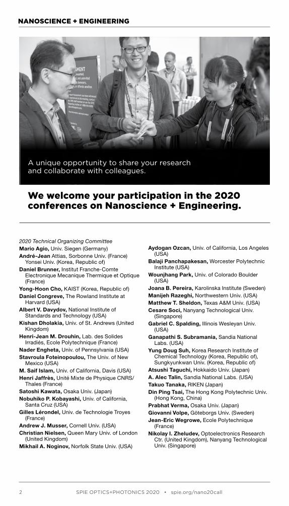
A unique opportunity to share your research and collaborate with colleagues.
We welcome your participation in the 2020 conferences on Nanoscience + Engineering.

Tel: +1 360 676 3290 • [email protected] • #SPIEOpticsPhotonics 3
2 SPIE OPTICS+PHOTONICS 2020 • spie.org/nano20call
SPIE International Headquarters PO Box 10 Bellingham, WA 98227-0010 USA Tel: +1 360 676 3290 / Fax: +1 360 647 1445 [email protected] / www.SPIE.org
SPIE Europe Office 2 Alexandra Gate Ffordd Pengam, Cardiff, CF24 2SA UK Tel: +44 29 2089 4747 / Fax: +44 29 2089 4750 [email protected] / www.SPIE.org
CALL FOR PAPERS
Contents
NANOSCIENCEOP101 Metamaterials, Metadevices, and
Metasystems 2020 (Engheta/Noginov/Zheludev) . . . . . . . . . . . . . . . . . . . . . . . . . 4
OP102 Active Photonic Platforms XII (Subramania/Foteinopoulou) . . . . . . . . . . 5
OP103 Plasmonics: Design, Materials, Fabrication, Characterization, and Applications XVIII (Tsai/Tanaka) . . . . . . . 7
OP104 Optical Trapping and Optical Micromanipulation XVII (Dholakia/ Spalding) . . . . . . . . . . . . . . . . . . . . . . . . . 8
OP105 Physical Chemistry of Semiconductor Materials and Interfaces IX (Nielsen/Congreve/Musser) . . . . . . . . . . . . . . . . . . 9
OP106 Low-Dimensional Materials and Devices 2020 (Kobayashi/Talin/Davydov/Islam) . 10
OP107 UV and Higher Energy Photonics: From Materials to Applications 2020 (Lérondel/Cho/Taguchi/Kawata) . . . . . . 11
OP110 Nanoengineering: Fabrication, Properties, Optics, Thin Films, and Devices XVII (Panchapakesan/Attias/ Park) . . . . . . . . . . . . . . . . . . . . . . . . . . . 12
OP111 Enhanced Spectroscopies and Nanoimaging 2020 (Verma/Suh) . . . . . 15
OP112 Emerging Topics in Artificial Intelligence 2020 (Volpe/Pereira/ Brunner/Ozcan) . . . . . . . . . . . . . . . . . . . 16
QUANTUM SCIENCES AND TECHNOLOGYOP113 Spintronics XIII (Drouhin/Wegrowe/
Razeghi/Jaffres) . . . . . . . . . . . . . . . . . . . 18
OP114 Quantum Nanophotonic Materials, Devices, and Systems 2020 (Soci/Sheldon/Agio) . . . . . . . . . . . . . . . . . . . . 19
OP431 Quantum Communications and Quantum Imaging XVIII (Deacon) . . . . 20
Abstract Submission . . . . . . . . . . . . . . . . . . . . . 23
General Information . . . . . . . . . . . . . . . . . . . . . . 24
SYMPOSIUM CHAIRS AND CO-CHAIRS
Symposium Chairs
Reuven GordonUniv. of Victoria (Canada)
Natalia M. LitchinitserDuke Univ. (USA)
Symposium Co-chairs
Halina Rubinsztein-DunlopThe Univ. of Queensland (Australia)
Mark L. BrongersmaGeballe Lab. for Advanced Materials (GLAM) (USA)
New
New

Tel: +1 360 676 3290 • [email protected] • #SPIEOpticsPhotonics 5
4 SPIE OPTICS+PHOTONICS 2020 • spie.org/nano20call
NANOSCIENCE
METAMATERIALS, METADEVICES, AND METASYSTEMS 2020 (OP101)Conference Chairs: Nader Engheta, Univ. of Pennsylvania (USA); Mikhail A. Noginov, Norfolk State Univ. (USA); Nikolay I. Zheludev, Optoelectronics Research Ctr. (United Kingdom), Nanyang Technological Univ. (Singapore)
Program Committee: Andrea Alù, The Univ. of Texas at Austin (USA); Alexandra Boltasseva, Purdue Univ. (USA); Igal Brener, Sandia National Labs. (USA); Mark Brongersma, Standford Univ. (USA); Joshua D. Caldwell, U.S. Naval Research Lab. (USA); Luca Dal Negro, Boston Univ. (USA); Jennifer A. Dionne, Stanford Univ. (USA); Jonathan A. Fan, Stanford Univ. (USA); Javier García de Abajo, ICFO - Institut de Ciències Fotòniques (Spain); Behrad Gholipour, Univ. of Alberta (Canada); Harald W. Giessen, Univ. Stuttgart (Germany); Yuri S. Kivshar, The Australian National Univ. (Australia); Jacob B. Khurgin, Johns Hopkins Univ. (USA); Uriel Levy, The Hebrew Univ. of Jerusalem (Israel); Alexander V. Kildishev, Purdue Univ. (USA); Natalia M. Litchinitser, Univ. at Buffalo (USA); Peter Nordlander, Rice Univ. (USA); Gennady B. Shvets, The Univ. of Texas at Austin (USA); David R. Smith, Duke Univ. (USA); Mark I. Stockman, Georgia State Univ. (USA); Sergei Tretyakov, Aalto Univ. School of Science and Technology (Finland); Din Ping Tsai, National Taiwan Univ. (Taiwan); Augustine M. Urbas, Air Force Research Lab. (USA); Martin Wegener, Karlsruher Institut für Technologie (Germany); Jeong Weon Wu, Ewha Womans Univ. (Korea, Republic of); Xiang Zhang, Univ. of California, Berkeley (USA)
Metamaterials and artificial electromagnetic media that are structured on the subwavelength scale were initially suggested for the negative-index ‘superlens’. Later, as metamaterials became a paradigm for engineering electromagnetic space and controlling the propagation of waves, the field of transformation optics was born. The research agenda is now focused on achieving quantum, tunable, switchable, nonlinear, sensing and data processing functionalities as well as control of light-matter interactions in weak and strong coupling regimes. This heralds the emergence of the new fields of metadevices and metasystems. The conference is a platform to discuss cutting-edge research on photonic, terahertz, microwave, thermal, acoustic and mechanical metamaterials, metadevices and metasystems with advanced functionalities at-tained through the exploitation of the entire plethora of quantum and classical mesoscale and nanoscale forces and interactions.
ABSTRACTS DUE: 12 February 2020AUTHOR NOTIFICATION: 20 April 2020 The contact author will be notified of acceptance by email.
Save the dateMANUSCRIPT DUE DATE:29 July 2020PLEASE NOTE: Submissions imply the intent of at least one author to register, attend the symposium, present the paper as scheduled, where it is an oral or poster presentation, and submit a full manuscript by the deadline.
Tel: +1 360 676 3290 • [email protected] • #SPIEOpticsPhotonics 5
4 SPIE OPTICS+PHOTONICS 2020 • spie.org/nano20call
CALL FOR PAPERS
ACTIVE PHOTONIC PLATFORMS XII (OP102)Conference Chairs: Ganapathi S. Subramania, Sandia National Labs. (USA); Stavroula Foteinopoulou, The Univ. of New Mexico (USA)
Program Committee: Andrea Alù, The City Univ. of New York (USA); Koray Aydin, Northwestern Univ. (USA); Harish Bhaskaran, Univ. of Oxford (United Kingdom); Paul V. Braun, Univ. of Illinois at Urbana-Champaign (USA); Che Ting Chan, Hong Kong Univ. of Science and Technology (Hong Kong, China); Zhigang Chen, Nankai Univ. (China), San Francisco State Univ. (USA); Dmitry N. Chigrin, RWTH Aachen Univ. (Germany); Shanhui Fan, Stanford Univ. (USA); Didier Felbacq, Univ. Montpellier (France); Juejun Hu, Massachusetts Institute of Technology (USA); Stephen Hughes, Queen’s Univ. (Canada); Boubacar Kante, Univ. of California, San Diego (USA); Mercedeh Khajavikhan, Univ. of Southern California (USA); Alexander V. Kildishev, Purdue Univ. (USA); Nathaniel Kinsey, Virginia Commonwealth Univ. (USA); Yuri S. Kivshar, The Australian National Univ. (Australia); A. Femius Koenderink, AMOLF (Netherlands); Aude L. Lereu, Institut Fresnel (France); Cefe López, Consejo Superior de Investigaciones Científicas (Spain); Liam O’Faolain, Cork Institute of Technology (Ireland), Tyndall National Institute (Ireland); Rupert F. Oulton, Imperial College London (United Kingdom); Nicolae-Coriolan Panoiu, Univ. College London (United Kingdom); Ruwen Peng, Nanjing Univ. (China); Ekaterina Poutrina, Air Force Research Lab. (USA); Michelle L. Povinelli, The Univ. of Southern California (USA); Subramaniam Anantha Ramakrishna, Indian Institute of Technology Kanpur (India); Christophe Sauvan, Lab. Charles Fabry (France); Jörg Schilling, Martin-Luther-Univ. Halle-Wittenberg (Germany); Gennady B. Shvets, Cornell Univ. (USA); Volker J. Sorger, The George Washington Univ. (USA); Isabelle Staude, Friedrich-Schiller-Univ. Jena (Germany); Andrey A. Sukhorukov, The Australian National Univ. (Australia); Philippe Tassin, Chalmers Univ. of Technology (Sweden); Kosmas L. Tsakmakidis, National and Kapodistrian Univ. of Athens (Greece); Georgios Veronis, Louisiana State Univ. (USA); Daniel M. Wasserman, The Univ. of Texas at Arlington (USA); Sharon M. Weiss, Vanderbilt Univ. (USA)
Platforms comprising artificially patterned materials exploit the synergy between material photonic re-sponses and structural form to enable transformative light-matter interactions which continually push for-ward the state-of-the art in light control capabilities. While tremendous progress has been made with only passive materials, such as metals and dielectrics, the potential of photonic platforms transcends into new unexplored domains when active material and/or material with tunable or dynamic photonic proper-ties are incorporated. Examples of such material are gain or non-linear media, phase-change materials, magneto-photonic material, 2D materials, as well as quantum emitters. Structured material platforms with active components can enable entirely new regimes of light control that is crucial to a wide range of ap-plications including chipscale all-optical computing and communications, nanoscale thresholdless lasers, modulator, thermal management and detector devic-es, as well as biological/chemical sensors.
The Active Photonic Platforms XII conference aims to bring together scientists and engineers working in the newest developments in fundamentals and applications of structured-material platforms for active, dynamic, and tunable control of light. Topics will cover active photonic platforms functional across the EM spectrum, from THz to UV frequencies, as well as new exotic types of light propagation, which could open entirely new directions in active photonics. Contributions from academia, government, industry, and other research organizations are solicited in areas including:
• theory and modeling approaches for non-linear and gain photonic media
• non-linear optical phenomena, materials, and devices
• novel harmonic generation and frequency mixing phenomena
• modeling and experimental realization of time-dependent photonic responses
• tunable and dynamically changeable optical properties and photonic devices
• dynamically reconfigurable platforms and photonic effects
• novel lasing platforms, nanolasers, and integrable chipscale light sources
• emission control in structured photonic environment: weak and strong coupling, cavity QED; polariton, quantum-dot, and random lasers
• physics and applications of nanoscale sources (e.g. quantum dots, quantum wires, NV-centers etc.) for photonic devices
• PT-symmetric, non-Hermitian and pseudo-Hermitian photonic systems
• topological and non-reciprocal photonic platforms
• phase-change materials for photonic devices • photonic memory and neuromorphic devices • photonic structures for quantum information:
non-classical sources and detectors • graphene- and carbon-based materials for
photonic and optoelectronic devices
Submit your abstract today: spie.org/nano20call
Continued
Tel: +1 360 676 3290 • [email protected] • #SPIEOpticsPhotonics 7
6 SPIE OPTICS+PHOTONICS 2020 • spie.org/nano20call
NANOSCIENCE
• photonic platforms with atomically thin materials such as hBN or transition-metal-dichalcogenides or their heterostructures (e.g. Van der Waals heterostructures)
• novel magneto-photonic phenomena and platforms
• advances in fabrication of photonic structures with active materials
• novel absorption and thermal management platforms
• photovoltaics, thermophotovoltaics, and photodetectors
• chemical sensors and biosensors based on active control of light
• opto-fluidic and optomechanical tunable devices.
This conference will confer an award for the best oral presentation by a student author. Only contributed presentations both submitted by a student on or before 12 February 2020, and presented by a student author are eligible for this award (the submitting and presenting author should be a student at the time of the abstract submission). The award winner(s), announced at the conclusion of the meeting, will be presented with an original SPIE award certificate, and receive a special mention in the introduction of the conference proceedings volume.
ACTIVE PHOTONIC PLATFORMS XII (OP102) continued
New data laws are in effectUnless you opt in to receive email
from us, you will not receive any SPIE info about SPIE Optics + Photonics.
spie.org/signup
Tel: +1 360 676 3290 • [email protected] • #SPIEOpticsPhotonics 7
6 SPIE OPTICS+PHOTONICS 2020 • spie.org/nano20call
CALL FOR PAPERS
PLASMONICS: DESIGN, MATERIALS, FABRICATION, CHARACTERIZATION, AND APPLICATIONS XVIII (OP103)Conference Chairs: Din Ping Tsai, The Hong Kong Polytechnic Univ. (Hong Kong, China); Takuo Tanaka, RIKEN (Japan)
Program Committee: Martin Aeschlimann, Technische Univ. Kaiserslautern (Germany); Hatice Altug, Ecole Polytechnique Fédérale de Lausanne (Switzerland); Harry A. Atwater Jr., California Institute of Technology (USA); David J. Bergman, Tel Aviv Univ. (Israel); Humeyra Caglayan, Tampere Univ. (Finland); Che Ting Chan, Hong Kong Univ. of Science and Technology (Hong Kong, China); Yun-Chorng Chang, Academia Sinica (Taiwan); Harald W. Giessen, Univ. Stuttgart (Germany); Naomi J. Halas, Rice Univ. (USA); Dai-Sik Kim, Seoul National Univ. (Korea, Republic of); Wakana Kubo, Tokyo Univ. of Agriculture and Technology (Japan); Laurens K. Kuipers, FOM Institute for Atomic and Molecular Physics (Netherlands); Mikhail Lapine, The Univ. of Sydney (Australia); Ai Qun Liu, Nanyang Technological Univ. (Singapore); Yu-Jung Lu, National Taiwan Univ. (Taiwan); Olivier J. F. Martin, Ecole Polytechnique Fédérale de Lausanne (Switzerland); Peter Nordlander, Rice Univ. (USA); George C. Schatz, Northwestern Univ. (USA); Tigran V. Shahbazyan, Jackson State Univ. (USA); Vladimir M. Shalaev, Purdue Univ. (USA); Gennady B. Shvets, Institute for Fusion Studies (USA); Niek F. van Hulst, ICFO - Institut de Ciències Fotòniques (Spain); Prabhat Verma, Osaka Univ. (Japan); Hongxing Xu, Wuhan Univ. (China); Shumin Xiao, Harbin Institute of Technology Shenzhen Graduate School (China); Nikolay I. Zheludev, Optoelectronics Research Ctr. (United Kingdom), Nanyang Technological Univ. (Singapore)
Plasmonics: Design, Materials, Fabrication, Charac-terization, and Applications is currently undergoing intense developments. Novel plasmonic materials, structures, and phenomena covered under this topic span broad multidisciplinary interests from funda-mental optics, physics, and chemistry to applications in nanophotonics, biophotonics, green photonics, and biomedicine.
The Plasmonics: Design, Materials, Fabrication, Char-acterization, and Applications conference requires a 500-word Abstract for Review.
Papers are solicited in the following areas:
THEORY, SIMULATION, AND DESIGN ACROSS ALL SUBAREAS• plasmonic phenomena and effects • ultrafast plasmonic effects and coherent control • plasmon polaritonics • surface-enhanced Raman scattering • plasmon-enhanced nonlinear phenomena • luminescence enhancement and quenching • quantum nanoplasmonics: QED effects, plasmon-
assisted quantum information, spasing, and nanolasing in plasmonic nanostructures
• microscopic theory of plasmonic properties • plasmonic imaging, including probe
ultramicroscopies, superlenses, and hyperlenses • novel plasmonic systems such as graphene • nanoplasmonic Fano resonances • electron-plasmon interactions • active plasmonics theory and design.
PLASMONIC MATERIALS AND STRUCTURE FABRICATIONS• nanofabrication of novel materials • chemical fabrication (bottom up) • lithographic and nanopatterning fabrication (top
down) • biomimetic and bio-inspired fabrication • active, tunable, and reconfigurable methods.
PLASMON C PHENOMENA AND CHARACTERIZATION• quantum entanglement and interference • spectroscopies (spectral, time-domain,
combined and multidimensional)
• local probes, nano-optics, and near field phenomena
• plasmon-assisted PEEM and energy-loss spectroscopy and visualization of plasmonic phenomena
• nonlinear and coherent optical properties • plasmonic enhanced phenomena: SERS, SEIRA,
nonlinear generation, luminescence, including molecules and nanostructured metals
• extraordinary transmission, diffractive, and refractive phenomena
• novel plasmonic systems such as graphene • Fano resonances in nanoplasmonic systems • plasmon polariton propagation in arrays of
metal nanoparticles and metal nanoplasmonic waveguides
• semiconductor plasmonics • fundamental physics of left-handed (negative-
refraction) plasmonic materials • active plasmonics • topological plasmonics.
PLASMONICS DEVICES AND SYSTEMS• plasmonic quantum devices • plasmonic sensors • nanoplasmonic waveguides and resonators • plasmonic nanocircuits; logical nanoscale
elements • plasmonic ultramicroscopies and nanoscopic
spectroscopies • plasmonics-assisted memory • plasmonic transistors • plasmonic nanolasers and spasers • nanoplasmonic antennas and their applications
in nanoscopes, photodetectors, solar cells, and lighting devices
• prospective graphene nanoplasmonic devices • sensing based on Fano resonances • modulators and switches based on active
plasmonics • low-frequency plasmons and their applications • solar energy harvesting • devices for telecommunications • medical and health applications.

Tel: +1 360 676 3290 • [email protected] • #SPIEOpticsPhotonics 9
8 SPIE OPTICS+PHOTONICS 2020 • spie.org/nano20call
NANOSCIENCE
OPTICAL TRAPPING AND OPTICAL MICROMANIPULATION XVII (OP104)Conference Chairs: Kishan Dholakia, Univ. of St. Andrews (United Kingdom); Gabriel C. Spalding, Illinois Wesleyan Univ. (USA)
Program Committee: Ashley R. Carter, Amherst College (USA); Reuven Gordon, Univ. of Victoria (Canada); Catherine M. Herne, State Univ. of New York at New Paltz (USA); Masud Mansuripur, College of Optical Sciences, The Univ. of Arizona (USA); James Millen, King’s College London (United Kingdom); David C. Moore, Yale Univ. (USA); Justus C. Ndukaife, Vanderbilt Univ. (USA); Lene Broeng Oddershede, Niels Bohr Institute (Denmark); Daniel H. Ou-Yang, Lehigh Univ. (USA); Daryl Preece, Univ. of California, San Diego (USA); Ruben Ramos-Garcia, Instituto Nacional de Astrofísica, Óptica y Electrónica (Mexico); Halina Rubinsztein-Dunlop, The Univ. of Queensland (Australia); Nick Vamivakas, Univ. of Rochester (USA); Yuebing Zheng, The Univ. of Texas at Austin (USA)
2020 aims to promote a vision looking forward, for the next extensions of what we celebrate, quite generally, as the legacy of Arthur Ashkin, whose early work on optical trapping has spawned enor-mous productivity and enhancement of fundamental knowledge across the sciences.
This conference, each year, draws well over one hundred presentations and an even larger number of participants, and is clearly growing. Still, poster sessions take place with sufficient room and degree of refreshment to ensure an excellent level of interac-tion. Notably, this conference has a truly international character. The proceedings of the conference contain a large collection of relevant papers, making a valu-able contribution to the field. Early career researchers are especially encouraged and highlighted.
Papers are solicited on (but not restricted to) the following areas: • new fundamental physics • ”gonzo” trapping (i.e., trapping at extremes) • cavity optomechanics • high-sensitivity detectors • toward (or in) the quantum limit of opto-
mechanics • photonic devices for optically induced forces • shaping the flow of information: energy and
momentum • optical angular momentum • statistical mechanics of small systems • single molecule manipulation and study • using the photonic toolbox to study cells and
their organelles • studies of active swimmers and hydrodynamics • optofluidics and optically shaped structures • optically driven microrheology, mechanobiology,
and micromechanical properties • enhanced sensitivity and resolution of optical
force actuators • optical manipulation of matter through gaseous
media
• foundations of the electromagnetic theory of force and momentum
• radiation pressure, tractor beams, and solar sails • near-field micromanipulation, plasmonic, and
nanoparticle trapping • beam shaping and aberration and wavefront
correction • optical sorting, optical lab-on-a-chip, and
microfluidics • optically manipulated robotics and novel
samples • nanoscale assembly with optical forces • optical tweezers coupled with novel forms of
microscopy • alternative and hybrid force systems (e.g., hybrid
AFM-optical force systems, or combinations with acoustic, magnetic, or other forces)
• nonlinear optical responses mediated through forces (translation, electrostriction)
• optically bound matter • holographic optical systems: from speckle to
studies of neurons.
New data laws are in effectUnless you opt in to receive email
from us, you will not receive any SPIE info about SPIE Optics + Photonics.
spie.org/signup
Tel: +1 360 676 3290 • [email protected] • #SPIEOpticsPhotonics 9
8 SPIE OPTICS+PHOTONICS 2020 • spie.org/nano20call
CALL FOR PAPERS
PHYSICAL CHEMISTRY OF SEMICONDUCTOR MATERIALS AND INTERFACES IX (OP105)Conference Chairs: Christian Nielsen, Queen Mary Univ. of London (United Kingdom); Daniel Congreve, The Rowland Institute at Harvard (USA)
Conference Co-Chair: Andrew J. Musser, Cornell Univ. (USA)
Program Committee: John B. Asbury, The Pennsylvania State Univ. (USA); Artem A. Bakulin, Imperial College London (United Kingdom); Natalie Banerji, Univ. Bern (Switzerland); Hugo A. Bronstein, Univ. of Cambridge (United Kingdom); Jenny Clark, The Univ. of Sheffield (United Kingdom); Felix Deschler, Technische Univ. München (Germany); Alexandre Fürstenberg, Univ. de Genève (Switzerland); David S. Ginger, Univ. of Washington (USA); Naomi S. Ginsberg, Univ. of California, Berkeley (USA); Paul A. Lane, The National Science Foundation (USA); Robert Lovrincic, Technische Univ. Braunschweig (Germany); Paul Meredith, Swansea Univ. (United Kingdom); Linda A. Peteanu, Carnegie Mellon Univ. (USA); Lee J. Richter, National Institute of Standards and Technology (USA); Carlos Silva, Georgia Institute of Technology (Canada); Sergei Tretiak, Los Alamos National Lab. (USA); Lauren Webb, The Univ. of Texas at Austin (USA); Omer Yaffe, Weizmann Institute of Science (Israel)
Physical processes which are controlled by the mate-rial properties of a semiconductor play an essential role in many physico-chemical applications, ranging from energy conversion and generation to catalysis and biological membranes. Recent developments in organic and hybrid (nano-) materials highlight the importance of surfaces and interfaces in quantum confined systems. At the same time, the study of the excited state properties in bulk materials, and their connection to material properties, such as structure and elemental composition, remains a relevant topic. The detailed study of the physics and physical chem-istry in nanomaterials and at their interfaces led to the development of specialized experimental and theoretical techniques with increasing complexity. New forms of nonlinear spectroscopy, imaging, and scanning-probe techniques continue to emerge in conjunction with sophisticated theoretical methods capable of treating correlated systems of increasing size and over timescales of femto- to nanoseconds.
The intent of this conference is to bring together an interdisciplinary group of scientists from academia, industry, and government laboratories who study fundamental processes of emerging and established semiconductor materials, and their interfaces, from bulk to the nanoscale.
For 2020 the scope of the conference will focus on the following topics: • physical chemistry of hybrid perovskite materials • photophysics of emerging semiconductor
materials and nanostructures • electron and energy transfer mechanisms at
interfaces • physical processes in solar energy conversion • exciton physics in semiconductors • carrier transport in complex systems • confinement effects in nanostructures • physical understanding of biological and
bioelectronics systems • emerging experimental tools to study interfaces
and nanomaterials • advances in modeling of electronic processes in
semiconductors and nanomaterials • multidimensional spectroscopies • structure-property relations in nanomaterials • interface engineering.
ABSTRACTS DUE: 12 February 2020AUTHOR NOTIFICATION: 20 April 2020 The contact author will be notified of acceptance by email.
Save the dateMANUSCRIPT DUE DATE:29 July 2020PLEASE NOTE: Submissions imply the intent of at least one author to register, attend the symposium, present the paper as scheduled, where it is an oral or poster presentation, and submit a full manuscript by the deadline.
Tel: +1 360 676 3290 • [email protected] • #SPIEOpticsPhotonics 11
10 SPIE OPTICS+PHOTONICS 2020 • spie.org/nano20call
NANOSCIENCE
Submit your abstract today: spie.org/nano20call
LOW-DIMENSIONAL MATERIALS AND DEVICES 2020 (OP106)Conference Chairs: Nobuhiko P. Kobayashi, Univ. of California, Santa Cruz (USA); A. Alec Talin, Sandia National Labs. (USA); Albert V. Davydov, National Institute of Standards and Technology (USA)
Conference Co-Chair: M. Saif Islam, Univ. of California, Davis (USA)
Program Committee: Deji Akinwande, The Univ. of Texas at Austin (USA); Kristine A. Bertness, National Institute of Standards and Technology (USA); Sonia Conesa-Boj, Technische Univ. Delft (Netherlands); Alexey Koposov, Institute for Energy Technology (Norway); Andrey Krayev, HORIBA Scientific (USA); Marina S. Leite, Univ. of Maryland, College Park (USA); Paola Prete, Istituto per la Microelettronica e Microsistemi (Italy); Volker J. Sorger, The George Washington Univ. (USA); George T. Wang, Sandia National Labs. (USA); Sanshui Xiao, Technical Univ. of Denmark (Denmark)
Low-dimensional material systems possessing at least one of their dimensions in the nanometer scale offer intriguing physical properties and undiscov-ered pathways toward revolutionary new device concepts for flexible and transparent electronics, photonics, quantum computing, and other advanced applications. Fabrication of quantum dots, nanow-ires, ultra-thin films, and heterostructures result in building blocks that reveal a wealth of interesting physical properties including quantum phenomena. Control of synthesis and processing at the nanometer scale offers unprecedented opportunities to tailor microscopic and macroscopic physical properties of such material systems. To further pursue these tremendous opportunities, many fundamental questions need to be addressed and technological barriers need to be overcome. This conference pro-vides a forum for the presentation and discussion of synthesis, processing, and characterization of low-dimensional materials tailored to their unique and peculiar physical properties. Design, fabrication, and characterization of novel device platforms that employ low-dimensional materials are also of inter-est, as well as interfacing and integration of such devices toward novel electronics, photonics, sensors, and energy conversion and storage.
Topics of interest include: • fabrication of zero-dimensional (core-shell
nanoparticles, quantum dots), one-dimensional (nanowires and nanorods), and two-dimensional (van-der-Waals layers such as transition metal dichalcogenides), and their device integration
• templated, catalyzed and uncatalyzed, tip assisted, field induced, locally heated synthesis methods of low-dimensional materials
• self-limiting deposition technique such as atomic layer deposition (ALD) that can produce ultrathin and conformal thin film structures for many applications including thin film devices, display technology, energy storage and capture, solid state lighting
• exploration of strain and extended defects effect on synthesis and spatial ordering of nanoscale structures and on their optical and transport properties
• introduction of electrically/optically active impurities and their roles in low-dimensional structures; dopant spatial distributions and segregation
• electrical contact formation and interface properties between nanoscale structures and metal contacts
• nanoscale synthesis compatible to and integral onto CMOS devices; scalable and mass-manufacturable interfacing for electronics, photonics, optoelectronics, sensing and energy conversion
• 3D heterogeneous integration, application of advanced patterning techniques for positioning and dimension control of nanostructures, integration with MEMS
• electrical, optical, mechanical and structural characterization, including in-situ and in-operando techniques, of the low-dimensional structures and device platforms; correlation of composition, microstructure, and defects to the material physical properties and device performance.
Tel: +1 360 676 3290 • [email protected] • #SPIEOpticsPhotonics 11
10 SPIE OPTICS+PHOTONICS 2020 • spie.org/nano20call
CALL FOR PAPERS
UV AND HIGHER ENERGY PHOTONICS: FROM MATERIALS TO APPLICATIONS 2020 (OP107)Conference Chairs: Gilles Lérondel, Univ. de Technologie Troyes (France); Yong-Hoon Cho, KAIST (Korea, Republic of); Atsushi Taguchi, Hokkaido Univ. (Japan)
Conference Co-Chair: Satoshi Kawata, Osaka Univ. (Japan)
Program Committee: Sanford A. Asher, Univ. of Pittsburgh (USA); Steve Blair, The Univ. of Utah (USA); Zhanghai Chen, Fudan Univ. (China); Yasin Ekinci, Paul Scherrer Institut (Switzerland); Torsten Frosch, Leibniz-Institut für Photonische Technologien e.V. (Germany); Naomi J. Halas, Rice Univ. (USA); Hans D. Hallen, North Carolina State Univ. (USA); Chennupati Jagadish, The Australian National Univ. (Australia); Junyong Kang, Xiamen Univ. (China); Yoichi Kawakami, Kyoto Univ. (Japan); Jong Kyu Kim, Pohang Univ. of Science and Technology (Korea, Republic of); Yasuaki Kumamoto, Kyoto Prefectural Univ. of Medicine (Japan); Paul T. Matsudaira, National Univ. of Singapore (Singapore); Eva Monroy, CEA Grenoble (France); Fernando Moreno, Univ. de Cantabria (Spain); Yukihiro Ozaki, Kwansei Gakuin Univ. (Japan); Sung-Jin Park, Univ. of Illinois (USA); Jérôme Plain, Univ. de Technologie de Troyes (France); Remo Proietti Zaccaria, Istituto Italiano di Tecnologia (Italy); Olivier Soppera, Univ. de Haute Alsace (France); Yunshan Wang, The Univ. of Utah (USA)
Recently, there has been a rapid and significant progress in the field of UV and higher energy pho-tonics (UV to EUV) due to the availability of new UV and high energy light sources. Nano-materials such as nucleotides and proteins known as the essential biomolecules in living cells and semiconducting or plasmonic materials used in advanced nano-devices are analyzed and detected, imaged, and/or manip-ulated with use of UV and higher energy photons. Starting from the material growth related aspects, this conference includes theories and novel concepts on UV and higher energy photonics. It also includes experiments and developments of methods and in-struments, which are used as devices for applications in catalysis, nano-lithography, nano-imaging, disin-fection, analytical sensing but also in nano-photonics, bio-medical photonics, materials sciences and green and environmental sciences. The chairs of the con-ference proudly announce that the Young Scientist Award will be given to two outstanding presentations respectively in oral and poster sessions. Successful candidates must convey significant scientific content with a demonstrated excellent style of presentation including questions and discussions. In addition, from 2020, potentially four contributed papers will be promoted to invited contribution.
UV AND HIGHER ENERGY MATERIALS AND LIGHT SOURCES • high band gap semiconductors • LEDs and lasers for UV and higher energy • nonlinear and ultrafast photonics for UV and
higher energy • fiber optics for UV and higher energy • photonic crystal fibers • high harmonic generation • UV to EUV optics and sources.
UV AND HIGHER ENERGY MICROSCOPY AND SPECTROSCOPY • resonant Raman microscopy • nonlinear microscopy • super-resolution microscopy • plasmonics in UV and DUV • coherent scattering imaging • resonance Raman spectroscopy • absorption spectroscopy • fluorescence spectroscopy.
APPLICATIONS OF UV, DEEP UV, VACUUM UV, AND EXTREME UV PHOTONICS • holography • lithography • photocatalysis • decontamination • material properties • materials processing • photoresists • photodissociation • photodamage • environmental analysis • energy production.
UV AND DEEP UV BIOSENSING AND ANALYSIS WITH UV AND HIGHER ENERGY PHOTONICS • biosensor and analysis • structure and dynamics of biomolecules • native fluorescence • photochemical effect on biomolecules.
New data laws are in effectUnless you opt in to receive email
from us, you will not receive any SPIE info about SPIE Optics + Photonics.
spie.org/signup

Tel: +1 360 676 3290 • [email protected] • #SPIEOpticsPhotonics 13
12 SPIE OPTICS+PHOTONICS 2020 • spie.org/nano20call
NANOSCIENCE
Submit your abstract today: spie.org/nano20call
NANOENGINEERING: FABRICATION, PROPERTIES, OPTICS, THIN FILMS, AND DEVICES XVII (OP110)Conference Chairs: Balaji Panchapakesan, Worcester Polytechnic Institute (USA); André-Jean Attias, Sorbonne Univ. (France), Yonsei Univ. (Korea, Republic of); Wounjhang Park, Univ. of Colorado Boulder (USA)
Program Committee: Bharat Bhushan, The Ohio State Univ. (USA); Stephane Bruynooghe, Carl Zeiss Jena GmbH (Germany); Francesco Chiadini, Univ. degli Studi di Salerno (Italy); Pankaj Kumar K. Choudhury, Univ. Kebangsaan Malaysia (Malaysia); Luca Dal Negro, Boston Univ. (USA); Maziar Ghazinejad, California State Univ., Fresno (USA); Frédéric Guittard, Univ. de Nice Sophia Antipolis (France); Sarah Haigh, The Univ. of Manchester (United Kingdom); Ghassan E. Jabbour, Arizona State Univ. (USA); Klaus Jäger, Helmholtz-Zentrum Berlin für Materialien und Energie GmbH (Germany); Yi-Jun Jen, National Taipei Univ. of Technology (Taiwan); Anders Kristensen, DTU Nanotech (Denmark); Akhlesh Lakhtakia, The Pennsylvania State Univ. (USA); Tom G. Mackay, The Univ. of Edinburgh (United Kingdom); H. Angus Macleod, Thin Film Center, Inc. (USA); Robert Magnusson, The Univ. of Texas at Arlington (USA); Dorota A. Pawlak, Institute of Electronic Materials Technology (Poland); Michael T. Postek, Retired, National Institute of Standards and Technology (USA); Dianne L. Poster, National Institute of Standards and Technology (USA); Geoffrey B. Smith, Univ. of Technology, Sydney (Australia); Motofumi Suzuki, Kyoto Univ. (Japan); Jun Tanida, Osaka Univ. (Japan); Tomas Tolenis, Ctr. for Physical Sciences and Technology (Lithuania); Chee Wei Wong, Columbia Univ. (USA); Wei Wu, The Univ. of Southern California (USA); Anatoly V. Zayats, King’s College London (United Kingdom)
Nanoengineering is an essential bridge that utilizes nanoscience and nanotechnology to enable a broad spectrum of totally new materials, functionalities, applications, devices, and products. Conventional photonic manufacturing technologies have extend-ed well into the nanometer regime. Over-extended technologies are pushing sizes and densities into ranges that challenge reliability and basic physics. Nanoengineering also allows for manipulating mat-ter at the nanoscale. Newly engineered materials, processes, ultrahigh precision and metrologies are emerging. Novel synthesized nanomaterials, based on 1D, 2D, and 3D architectures, nanocomposites and hierarchical assemblies based on such mate-rials offer exciting opportunities. Nanostructured thin films display unique phenomena, thus enabling the improvement of traditional applications or the development of novel applications. Newly attainable design and fabrication of miniature optical elements have enabled the development of micro/nano/quantum-scale optical, near field optics, and opto-electronic elements in ever more diverse application areas. New low power logic and memory devices, expanded functionality, systems on a chip, solar cells, energy storage devices, biotechnology, photonics, photovoltaics, molecular electronics and optics are emerging. Application areas are highly diversified and include telecommunications, data communica-tions, consumer electronics, microwave photonics, optical computing, neural networks, optical storage, non-volatile data storage, information display, optical imaging, printing, optical sensing, optical scanning, renewable energy harvest and storage, medical di-agnosis, chemical/biological/environmental sensing, new nanomechanic applications, and new medical devices and prosthetic methods.
Critical to this realization of robust nanomanufactur-ing is the development of appropriate instrumenta-tion, metrology, and standards. As novel applications emerge, the demand for highly sensitive and efficient measurement tools with the capability of rapid, au-tomated, and thorough coverage of large functional areas at high precision is emerging.
The newly upcoming nanotechnologies present new opportunities and challenges in materials processing, device design, and integration. Drivers for commer-cial deployment include increased functionality, small form factor, performance, reliability, cost, as well as renewable energy and climate change mitigation.
Papers are solicited in the areas of:
LIGHT-MATTER INTERACTIONS IN 1D AND 2D NANOMATERIALS• 1D and 2D photo-physics • photoconductivity and photocurrents in 1D and
2D nanomaterials and composites • novel architectures based on 1D and 2D
nanomaterials for enhanced light-matter interactions
• photo-thermal phenomenon in nanoscale materials and their composites
• novel devices based on 1D and 2D nanomaterials for photonics.

Tel: +1 360 676 3290 • [email protected] • #SPIEOpticsPhotonics 13
12 SPIE OPTICS+PHOTONICS 2020 • spie.org/nano20call
CALL FOR PAPERS
PHOTON UPCONVERSION• exploration of new photon upconversion
materials, nanomaterials, and nanostructures • synthesis and surface modification techniques
for photon upconversion materials • nanophotonic approach for photon upconversion
enhancement, including but, not limited to, plasmonic nanostructures, metamaterials, photonic crystals, and nanocavities
• applications of photon upconversion materials, including, but not limited to, solar energy conversion, imaging, sensing, and therapeutics
• theory and modeling of photon upconversion processes
• advanced spectroscopy and other characterizations of photon upconversion materials.
NANOSTRUCTURED THIN FILMS• fabrication techniques • characterization • homogenization studies and modeling • hybrid nanostructures • multifunctionality at the nanoscale • plasmonics • organic and inorganic nanostructured thin films • sculptured thin films • nanostructured porous thin films • two-dimensional materials • carbon-based nanostructures • topological insulators and photonic topological
insulators • functionalization of nanostructures • thin-film sensors • superhydrophobicity • biomedical applications • bioinspired and biomimetic thin films • structural evolution.
INNOVATIVE PATTERNING, MATERIALS ENGINEERING, NANOFABRICATION, AND NANOLITHOGRAPHY FOR PHOTONICS APPLICATIONS• electrospinning, imprinting, and embossing
techniques • fabrication, processing, and replication
techniques • directed self-assembly techniques • engineered nano- and micro-structured materials • synthesis of nanotubes, nanowires, and two-
dimensional materials such as graphene • stacked 2D atomic crystals • molecular patterning and ordering.
HIGH PRECISION NANOPOSITIONING AND FEEDBACK, NEW METROLOGIES FOR PHOTONICS• proximal probe manipulation techniques • nanomotors and actuators • nano-alignment techniques, tolerance • tribology nanotechnologies • new metrology instrumentation, methods, and
standards for measuring nanodevices • metrology for placement precision • novel measurement and inspection
methodologies • high resolution optics, including full-field,
near-field and scanning probe microscopy, scatterometry, and interferometric techniques
• x-ray techniques • synchrotron techniques • optical detectors for state of the art
instrumentation • particle beam (electron, ion) microscopy and
elemental analysis • atomic force microscopy.
NANOMANUFACTURING OF 1D AND 2D NANOMATERIALS FOR PHOTONICS APPLICATIONS• liquid phase exfoliation of 1D and 2D
nanomaterials • new developments in liquid phase exfoliation for
low cost nanomanufacturing • chemical vapor deposition of 1D and 2D
nanomaterials for manufacturing • new green synthesis methods for low cost
manufacturing of 1D and 2D nanomaterials • scalable manufacturing of nanocomposites
based on 1D and 2D nanomaterials • properties of scalable nanomanufactured
products • scalable nanomanufacturing: innovative device
architectures • scalable nanomanufacturing: what is the road
map?
DEVICES AND PROPERTIES OF NANOSTRUCTURES FOR PHOTONICS (EXPERIMENT AND/OR THEORY)• nanoelectronic and nanomagnetic devices and
structures • waveguiding nanodevices and nanostructures • nano-MEMS devices and structures • near field optics based devices • NOMS: Nano-Opto-Mechanical Systems • photovoltaic cells and structures
Continued
ABSTRACTS DUE: 12 February 2020AUTHOR NOTIFICATION: 20 April 2020 The contact author will be notified of acceptance by email.
Save the dateMANUSCRIPT DUE DATE:29 July 2020PLEASE NOTE: Submissions imply the intent of at least one author to register, attend the symposium, present the paper as scheduled, where it is an oral or poster presentation, and submit a full manuscript by the deadline.
Tel: +1 360 676 3290 • [email protected] • #SPIEOpticsPhotonics 15
14 SPIE OPTICS+PHOTONICS 2020 • spie.org/nano20call
NANOSCIENCE
• biological devices and structures • molecular devices and structures • atomic devices and structures • quantum devices and structures • nanosensors • smart mechanical actuators • 1D nanotubes • stacked 2D atomic crystals.
NANO- AND MICRO-OPTICS• physics, theory, design, modeling, and numerical
simulation of optical nano- and micro-structures • diffractive and refractive micro-structures for
beam shaping and manipulation • photonic microcircuits in silica, polymer, silicon,
compound semiconductors, ferroelectrics, magnetics, metals, and biomaterials
• 1D, 2D, and 3D photonic crystals • quantum dots, wells, and wires • guided-wave and free-space optical
interconnects • optical alignment, tolerance, and coupling • characterization (optical, electrical, structural,
etc.) • integration with guided-wave systems • integration with photonic devices including
VCSELs, modulators, and detectors • nano- and micro-optic-based optical
components, modules, subsystems, and systems for communications, information processing, computing, storage, photovoltaic power generation, information display, imaging, printing, scanning, and sensing
• graphene-and transition metal dichalcogenides based devices
• molecular devices.
ENERGY HARVESTING AND STORAGE NANOTECHNOLOGIES• nanostructured materials for efficient light
trapping, photon absorption, charge generation, charge transport, and current collection in photovoltaic cells and modules
• nanostructured solar cells • polymer solar cells based on 1D and 2D
nanomaterials • solar thermal phenomenon based on 1D and 2D
nanomaterials • photoelectrochemical cells based on 1D and 2D
nanomaterials
• nanocomposites, nanocoatings, and nanolubricants for power-generating wind turbines
• nanocomposites for smart behavior: reciprocity in electroactuation
• nanotechnologies for batteries and ultracapacitors, including powder-based, carbon-nanotube-based, silicon-nanowire-based and graphene-based electrodes.
COMMERCIALIZATION OF NANO- AND MICRO-STRUCTURE PHOTONIC AND OTHER DEVICES, MODULES, AND SYSTEMS• nanomanufacturing methodology • in-situ and in-operando inspection • 3D critical dimension metrology • characterization of nanostructured functional
surfaces • characterization of nano-objects used in novel
devices or products • assembly and packaging • reliability • novel concepts.
Submit your abstract today: spie.org/nano20call
NANOENGINEERING: FABRICATION, PROPERTIES, OPTICS, THIN FILMS, AND DEVICES XVII (OP110) continued
Tel: +1 360 676 3290 • [email protected] • #SPIEOpticsPhotonics 15
14 SPIE OPTICS+PHOTONICS 2020 • spie.org/nano20call
CALL FOR PAPERS
ENHANCED SPECTROSCOPIES AND NANOIMAGING 2020 (OP111)Conference Chairs: Prabhat Verma, Osaka Univ. (Japan); Yung Doug Suh, Korea Research Institute of Chemical Technology (Korea, Republic of), Sungkyunkwan Univ. (Korea, Republic of)
Program Committee: Katrin F. Domke, Max-Planck-Institut für Polymerforschung (Germany); Masayuki Futamata, Saitama Univ. (Japan); Tamitake Itoh, AIST (Japan); Dayong Jin, Univ. of Technology, Sydney (Australia); Satoshi Kawata, Osaka Univ. (Japan); Dangyuan Lei, City Univ. of Hong Kong (Hong Kong, China); Alfred J. Meixner, Eberhard Karls Univ. Tübingen (Germany); Yukihiro Ozaki, Kwansei Gakuin Univ. (Japan); Matthew A. Pelton, Univ. of Maryland, Baltimore County (USA); Markus B. Raschke, Univ. of Colorado Boulder (USA); Bin Ren, Xiamen Univ. (China); P. James Schuck, Columbia Univ. (USA); Zachary D. Schultz, The Ohio State Univ. (USA); Ze Xiang Shen, Nanyang Technological Univ. (Singapore); Takayuki Umakoshi, Osaka Univ. (Japan); Siva Umapathy, Indian Institute of Science, Bengaluru (India); Katherine A. Willets, Temple Univ. (USA); Peng Xi, Peking Univ. (China); Hongxing Xu, Wuhan Univ. (China); Renato Zenobi, ETH Zurich (Switzerland)
There is a huge demand for research tools allowing one to “see” and investigate materials and biological samples at a resolution of true nanoscale and to characterize and sense constituents at molecular levels as well to understand biochemical process at nanoscale. Optical techniques such as nanospec-troscopy and nanoimaging make this possible. Tools involving enhanced and confined light in optical spectroscopy and imaging have pushed the spatial resolution far beyond the diffraction limits of light and the detection sensitivity to new scales. Contin-uous improvements open ways to novel applications at the forefront of scientific knowledge.
The purpose of this interdisciplinary conference is to encompass all aspects of enhanced and confined light for nanospectroscopy and nanoimaging, in-cluding theory and novel concepts, experimental demonstration of novel concepts, major developmen-tal progress and applications to any field in science, in particular, biological, medical, chemical, and the material sciences.
Papers are solicited in (but not restricted to) the following areas:
NANOSPECTROSCOPIC AND SENSING TECHNIQUES• surface- and particle-enhanced Raman
spectroscopy (SERS, PERS) • surface-enhanced infrared absorption
spectroscopy (SEIRAS) • shell-isolated nanoparticle-enhanced Raman
spectroscopy (SHINERS) • stimulated Raman spectroscopy (SRS) at high
spatial resolution • dielectric-enhanced spectroscopies • enhanced spectroscopies for molecular sensing.
NEAR-FIELD NANOIMAGING TECHNIQUES• near-field scanning optical microscopy (NSOM/
SNOM) • tip-enhanced Raman scattering (TERS)
microscopy • tip-enhanced photoluminescence (TE-PL)
microscopy • tip-enhanced coherent anti-Stokes Raman
scattering (TE-CARS) microscopy.
OTHER NANOSCALE OPTICAL SPECTROSCOPIC/SENSING/IMAGING TECHNIQUES• new/unconventional experimental techniques for
nanospectroscopy and nanoimaging • new/unconventional techniques for molecular
detection and sensing • growth/fabrication of plasmonic/dielectric
materials for nanospectroscopy and nanoimaging • growth/fabrication of plasmonic devices for
molecular sensing • theoretical/simulation studies in related fields of
nanospectroscopy • other nonlinear optical spectroscopy/microscopy
at nanoscale.
New data laws are in effectUnless you opt in to receive email
from us, you will not receive any SPIE info about SPIE Optics + Photonics.
spie.org/signup

Tel: +1 360 676 3290 • [email protected] • #SPIEOpticsPhotonics 17
16 SPIE OPTICS+PHOTONICS 2020 • spie.org/nano20call
EMERGING TOPICS IN ARTIFICIAL INTELLIGENCE 2020 (OP112)Conference Chairs: Giovanni Volpe, Göteborgs Univ. (Sweden); Joana B. Pereira, Karolinska Institute (Sweden); Daniel Brunner, Institut Franche-Comte Electronique Mecanique Thermique et Optique (France); Aydogan Ozcan, Univ. of California, Los Angeles (USA)
Program Committee: Jonas Andersson, Syntronic (Sweden); George Barbastathis, Massachusetts Institute of Technology (USA); Frank Cichos, Univ. Leipzig (Germany); Margaretta Colangelo, Deep Knowledge Ventures (USA); Joni Dambre, Univ. Ghent (Belgium); Danny Krautz, Optize (Germany); Alireza Marandi, Caltech (USA); Armand Niederberger, Noodle.ai (USA); Bert Jan Offrein, IBM Research - Zürich (Switzerland); Demetri Psaltis, Ecole Polytechnique Fédérale de Lausanne (Switzerland); Stephan Reitzenstein, Technische Univ. Berlin (Germany); Yair Rivenson, Univ. of California, Los Angeles (USA); Elena Rodriguez-Vieitez, Karolinska Institute (Sweden); Halina Rubinsztein-Dunlop, The Univ. of Queensland (Australia); Bhavin J. Shastri, Queen’s Univ. (Canada); Guohai Situ, Shanghai Institute of Optics and Fine Mechanics, Chinese Academy of Sciences (China); Volker J. Sorger, The George Washington Univ. (USA); Evelyn Tang, Max Planck Institute for Dynamics and Self-Organization (Germany)
This conference provides a forum for a highly inter-disciplinary community combining artificial intel-ligence with photonics, microscopy, active matter, biomedicine, and brain connectivity. Importantly, this conference includes topics outside the core expertise of optics and photonics. Photonics and machine learning have become decisively interdisciplinary, and we expect additional synergy and inspiration through this open-minded approach.
This conference will also actively engage industry, important to foster commercialization and utilization opportunities.
By bringing together experts from different fields and backgrounds, this conference will provide new fundamental insights, technological applications, and commercialization opportunities.
The topics that will be covered are: • data acquisition and analysis through photonic
subsystems, e.g., time series, images, video feature tracking, optical signal processing
• simulation and design of photonic components and circuits
• adaptive control of experimental setups through more robust and resilient feedback cycles
• enhanced computational microscopy using artificial intelligence
• fundamental aspects of photonic non-digital computing
• integrated photonics and nonlinear optical components for next generation computing
• alternative computing concepts such as neural networks and Ising machines to overcome the end of Moore and Dennard scaling
• enhanced precision medicine, e.g., virtual tissue staining, early diagnosis, and personalized treatments
• artificial intelligence for analysis of brain connectivity
• biomimetic and neuromorphic computational architectures
• embodied intelligence in nature and technology • evolution of adaptive behaviors in biological
systems • engineering collective behaviors in robotic
swarms • human brain haptic device interfaces • physical insight and interpretability of artificial
intelligence models • limitations and criticism of the use of artificial
intelligence.
The keynote and invited presentations will provide an exciting and broad view of this interdisciplinary research effort. The poster sessions will take place with sufficient room and refreshments to ensure an excellent level of interaction.
Abstracts are solicited on (but not restricted to) the following areas:
ARTIFICIAL INTELLIGENCE FOR PHOTONICS• optical system design using machine learning • machine learning-based solutions to inverse
problems in optics • spectroscopy enhancement using machine
learning.
ARTIFICIAL INTELLIGENCE FOR MICROSCOPY• computational microscopy • data-driven optical reconstruction methods • digital video microscopy • generation of training datasets.
ARTIFICIAL INTELLIGENCE FOR BIOMEDICINE• machine learning-enhanced optical imaging and
sensing • image segmentation • virtual tissue staining • artificial intelligence as a tool to enhance
decision-making in personalized medicine and drug screening
• multiple-sources data structuring and combination in complex biomedical decision-making
• legal and ethical aspects of the use of artificial intelligence as a tool for decision-making in medicine.
ARTIFICIAL INTELLIGENCE FOR OPTICAL TRAPPING• particle detection • optical trap calibration • feedback control.
NANOSCIENCE
Tel: +1 360 676 3290 • [email protected] • #SPIEOpticsPhotonics 17
16 SPIE OPTICS+PHOTONICS 2020 • spie.org/nano20call
ARTIFICIAL INTELLIGENCE FOR SOFT AND ACTIVE MATTER• data acquisition using machine learning • data analysis using machine learning • de-noising using machine learning • reinforcement learning in physical systems • dynamics of complex systems • intelligent foraging • navigation and search strategies.
NEUROMORPHIC COMPUTING• next generation materials for optical nonlinearity • integration of ultra-parallel photonic
architectures • beyond 2D substrates • physical substrates for machine learning
applications.
OPTICAL NEURAL NETWORKS• learning in optical systems • applications for optical neural networks • scalability of optical neural networks.
AUTONOMOUS ROBOTS• swarming robots • feedback control • elaboration of sensorial inputs • decision making.
BIOLOGICAL MODELS FOR ARTIFICIAL INTELLIGENCE• physical foundations of biological intelligence • translation of biological models to artificial
intelligence • collective motion in biological populations.
MACHINE LEARNING TO STUDY THE BRAIN• machine learning methods for image
segmentation • supervised and unsupervised models • multi-voxel pattern analysis • predictive modelling approaches.
ARTIFICIAL INTELLIGENCE FOR BRAIN CONNECTIVITY• measurement of brain activity and anatomy in
humans and animals • structural and functional connectomics • graph theoretical tools • clusters and subnetwork extraction • dimensionality reduction techniques to identify
brain networks.
MACHINE-BRAIN INTERFACES• detection of brain activity • haptic devices • feedback control through brain waves.
LIMITATIONS OF ARTIFICIAL INTELLIGENCE• the “black-box problem” of machine learning • interpretability, explainability, and uncertainty
quantification of machine-learning models • generalization power of machine-learning
models • model selection • development of objective benchmarks.
CALL FOR PAPERS
ABSTRACTS DUE: 12 February 2020AUTHOR NOTIFICATION: 20 April 2020 The contact author will be notified of acceptance by email.
Save the dateMANUSCRIPT DUE DATE:29 July 2020PLEASE NOTE: Submissions imply the intent of at least one author to register, attend the symposium, present the paper as scheduled, where it is an oral or poster presentation, and submit a full manuscript by the deadline.

Tel: +1 360 676 3290 • [email protected] • #SPIEOpticsPhotonics 19
18 SPIE OPTICS+PHOTONICS 2020 • spie.org/nano20call
SPINTRONICS XIII (OP113)Conference Chairs: Henri-Jean M. Drouhin, Lab. des Solides Irradiés, Ecole Polytechnique (France); Jean-Eric Wegrowe, Ecole Polytechnique (France); Manijeh Razeghi, Northwestern Univ. (USA)
Conference Co-Chair: Henri Jaffrès, Unité Mixte de Physique CNRS/Thales (France)
Program Committee: Claire Baraduc, CEA-Grenoble (France); Franco Ciccacci, Politecnico di Milano (Italy); Russell P. Cowburn, Univ. of Cambridge (United Kingdom); Scott A. Crooker, Los Alamos National Lab. (USA); Vincent Cros, Unité Mixte de Physique CNRS/Thales (France); Hanan Dery, Univ. of Rochester (USA); Rogério de Sousa, Univ. of Victoria (Canada); Michel I. Dyakonov, Univ. Montpellier 2 (France); Michael E. Flatté, The Univ. of Iowa (USA); Joseph S. Friedman, The Univ. of Texas at Dallas (USA); Pietro Gambardella, ETH Zurich (Switzerland); Jean-Marie George, Unité Mixte de Physique CNRS/Thales (France); Julie Grollier, Unité Mixte de Physique CNRS/Thales (France); Erez Hasman, Technion-Israel Institute of Technology (Israel); Tomás Jungwirth, Institute of Physics of the CAS, v.v.i. (Czech Republic); Giti A. Khodaparast, Virginia Polytechnic Institute and State Univ. (USA); Mathias Klaui, Univ. Konstanz (Germany); Daniel Lacour, Institut Jean Lamour (France); Connie H. Li, U.S. Naval Research Lab. (USA); Aurélien Manchon, King Abdullah Univ. of Science and Technology (Saudi Arabia); Xavier Marie, INSA - Univ. of Toulouse (France); Laurens W. Molenkamp, Julius-Maximilians-Univ. Würzburg (Germany); Hiro Munekata, Tokyo Institute of Technology (Japan); Hans T. Nembach, National Institute of Standards and Technology (USA); Yoshichika Otani, The Univ. of Tokyo (Japan); Vlad Pribiag, Univ. of Minnesota, Twin Cities (USA); Dafiné Ravelosona, Institut d’Électronique Fondamentale (France); Nicolas Rougemaille, Institut NÉEL (France); Georg Schmidt, Martin-Luther-Univ. Halle-Wittenberg (Germany); Jing Shi, Univ. of California, Riverside (USA); Vasily V. Temnov, Univ. du Maine (France); Luc Thomas, Headway Technology (USA); Evgeny Tsymbal, Univ. of Nebraska-Lincoln (USA); Olaf M. J. van ‘t Erve, U.S. Naval Research Lab. (USA); Joerg Wunderlich, Hitachi Cambridge Lab. (United Kingdom); Igor Zutic, Univ. at Buffalo (USA)
For years the spin degree of freedom has been directly used as an information support in nanome-ter-scale devices. Today applications mostly concern the huge market of hard-drive read heads, nonvolatile magnetic memories (MRAMs), or magnetic logic units. Recent developments are being considered for spin-based logic or quantum computing. New topics are emerging in frontier fields, e.g. Skyrmions and domain-wall manipulation, topological insulators, Majorana fermions, spin photonics and spin optics (the latter being based on recent developments in plasmonics), or spin-caloric phenomena. These advances make use of the fascinating developments of new materials.
The purpose of the conference is to provide a broad overview of the state-of-the-art and perspectives, bringing together experts from different com-munities: fundamental physics (experimental and theoretical), materials science and chemistry, fabri-cation processes and industrial developments, etc. Contributions for this conference are encouraged in particular in the following areas: • spin-coherence, semiconductor spin physics,
quantum wells and quantum dots • magnetic nanostructures, micromagnetism, spin-
precession, and magnonics • spin-injection, spin-transfer, spin-Hall and related
effects • new materials (graphene and chalcogenides,
oxides, organics, etc.) • topological matter, skyrmions • new structures and applications
(magnetoresistive devices, MRAMs, spin logic, crystalline tunnel barriers, etc.)
• neuromorphic computing • spin photonics, spin lasers, and spin optics.

Tel: +1 360 676 3290 • [email protected] • #SPIEOpticsPhotonics 19
18 SPIE OPTICS+PHOTONICS 2020 • spie.org/nano20call
QUANTUM SCIENCES AND TECHNOLOGY
QUANTUM NANOPHOTONIC MATERIALS, DEVICES, AND SYSTEMS 2020 (OP114)Conference Chairs: Cesare Soci, Nanyang Technological Univ. (Singapore); Matthew T. Sheldon, Texas A&M Univ. (USA); Mario Agio, Univ. Siegen (Germany)
Program Committee: Igor Aharonovich, Univ. of Technology, Sydney (Australia); Vikas Anant, Photon Spot, Inc. (USA); Iñigo Artundo, VLC Photonics (Spain); Jennifer A. Dionne, Stanford Univ. (USA); Andrei Faraon, Caltech (USA); Mohammad Hafezi, Joint Quantum Institute (USA); Zubin Jacob, Purdue Univ. (USA); Christian Kurtsiefer, National Univ. of Singapore (Singapore); Mark Lawrence, Stanford Univ. (USA); Peter Lodahl, Niels Bohr Institute (Denmark); Marko Loncar, Harvard John A. Paulson School of Engineering and Applied Sciences (USA); Chao-Yang Lu, Univ. of Science and Technology of China (China); Patrick Maletinsky, Univ. Basel (Switzerland), Qnami (Switzerland); Maiken H. Mikkelsen, Duke Univ. (USA); Prineha Narang, Harvard Univ. (USA); Kae Nemoto, National Institute of Informatics (Japan); Jeremy L. O’Brien, Univ. of Bristol (United Kingdom); Teri W. Odom, Northwestern Univ. (USA); Jian-Wei Pan, Univ. of Science and Technology of China (China); Pascale Senellart, Lab. de Photonique et de Nanostructures (France); Andrew J. Shields, Toshiba Research Europe Ltd. (United Kingdom); Kartik Srinivasan, National Institute of Standards and Technology (USA); Daniel L. Stick, Sandia National Labs. (USA); Mark Tame, Stellenbosch Univ. (South Africa); Wolfgang Tittel, Univ. of Calgary (Canada); Ewold Verhagen, AMOLF (Netherlands); Ulrike Woggon, Technische Univ. Berlin (Germany)
Optics and photonics enable devices that exploit the laws of quantum physics at a fundamental level, laying the ground for a second quantum revolution. Light is widely used in emerging quantum technolo-gies, for example to control and manipulate quantum states of matter, to generate and transmit qubits, to achieve quantum nonlinearities and many-body effects. In addition, advances in nanofabrication and circuit integration (e.g. silicon photonics, fiber optics, plasmonics) are crucial to translate proof of concepts into technological platforms for quantum simulations, metrology, sensing, imaging, communi-cation and computing.
Quantum nanophotonic materials, devices, and systems aims at establishing a multidisciplinary forum for physicists, material scientists, and optical engineers to discuss the current progress, challeng-es, and future directions of the burgeoning field of quantum nanophotonics. Contributions are solicited in areas focusing on:
MATERIAL PLATFORMS FOR QUANTUM PHOTONIC DEVICES• wide bandgap materials: diamond, silicon
carbide, rare earths • semiconductors: silicon, III-V and II-V compounds • two-dimensional materials: graphene, boron-
nitride, transition metal dicalcogenides • plasmonics, metamaterials and metasurfaces • nanoantennas • topological materials.
QUANTUM PHOTONIC DEVICES FOR SIMULATIONS, METROLOGY, SENSING, IMAGING, COMMUNICATION AND COMPUTING• nanoscale atom traps • single-photon sources and modulators • single-photon and photon-number discriminating
detectors • spin-photon interfaces for sensors and repeaters • quantum gates • optomechanical devices • quantum chemistry.
QUANTUM NANOPHOTONIC SYSTEMS• quantum key distribution and quantum random
number generators • quantum computers and simulators • quantum sensors based on solid-state systems
and atom chips • quantum engineering, including nanofabrication
and integration • quantum control, including error correction and
tolerance • quantum entanglement and imaging.
ABSTRACTS DUE: 12 February 2020AUTHOR NOTIFICATION: 20 April 2020 The contact author will be notified of acceptance by email.
Save the dateMANUSCRIPT DUE DATE:29 July 2020PLEASE NOTE: Submissions imply the intent of at least one author to register, attend the symposium, present the paper as scheduled, where it is an oral or poster presentation, and submit a full manuscript by the deadline.
Tel: +1 360 676 3290 • [email protected] • #SPIEOpticsPhotonics 21
20 SPIE OPTICS+PHOTONICS 2020 • spie.org/nano20call
QUANTUM SCIENCES AND TECHNOLOGY
Submit your abstract today: spie.org/nano20call
QUANTUM COMMUNICATIONS AND QUANTUM IMAGING XVIII (OP431)Conference Chair: Keith S. Deacon, U.S. Army Research Lab. (USA)
Program Committee: Stefania A. Castelletto, RMIT Univ. (Australia); Milena D’Angelo, Univ. degli Studi di Bari Aldo Moro (Italy); Warren P. Grice, Qubitekk (USA); Mark T. Gruneisen, Air Force Research Lab. (USA); Richard J. Hughes, Los Alamos National Lab. (Retired) (USA); Yoon-Ho Kim, Pohang Univ. of Science and Technology (Korea, Republic of); William J. Munro, NTT Basic Research Labs. (Japan); Kae Nemoto, National Institute of Informatics (Japan); Todd B. Pittman, Univ. of Maryland, Baltimore County (USA); Barry C. Sanders, Univ. of Calgary (Canada); Alexander V. Sergienko, Boston Univ. (USA); Oliver Slattery, National Institute of Standards and Technology (USA); Dmitry V. Strekalov, Jet Propulsion Lab. (USA); Shigeki Takeuchi, Kyoto Univ. (Japan); Arnold Tunick, U.S. Army Combat Capabilities Development Command (USA)
Quantum communications and quantum imaging are emerging technologies that promise great benefits beyond classical communications and classical im-aging - as well as great challenges. The objective of this conference is to provide a forum for scientists, researchers, and system developers in both fields and encourage technology exchange between the quantum communication and quantum imaging research communities. Papers are solicited on the following and related topics:
QUANTUM COMMUNICATIONS, QUANTUM INTERNET, AND QUANTUM INFORMATION • quantum free-space and fiber optics
communications and cryptography • quantum communications experimental
demonstrations • quantum key distribution (QKD), entangled QKD,
stochastic QKD, heralded QKD • quantum cryptography protocols • quantum probes • quantum communication security • quantum communications with orbital angular
momentum (OAM) states • quantum communication using entanglement • teleportation; continuous variable teleportation
counter-factual quantum communications • Bell-state analyzer development • nonlinear crystal and nonlinear fiber use in
generating and engineering entanglement • multiphoton and multiple-particle entangled
states and entangled beams • continuous and pulsed laser sources of entangled
photons • fundamental properties of the photon • qubit physics • single and multi-photon physics • squeezed states • slow/trapped light and photons • amplification and transmission of photon holes • quantum wavefunctions & measurements • quantum probability • quantum bi-photon physics • frequency and polarization entanglement • atmospheric quantum communication, satellite,
and technology applications • quantum satellites, quantum cube satellites • quantum UAV, drone, robot and aircraft research
and applications
• atmospheric effects on quantum communications systems
• atmospheric quantum communication propagation experiments, theory, simulation
• quantum computing with photons • optical/photonic/fiber quantum computing; novel
quantum computing • photon chips • quantum storage, gates, and control • single-photon sources • quantum algorithms • fine-grained quantum computing; few-qubit
quantum computing • quantum state engineering • quantum random number generation • quantum information communication • information in a photon • quantum data compression • compressive sensing and compressive imaging
with quantum information • nonclassical information from entangled states
and non-entangled states • non-local measurements • quantum secret sharing • quantum networks • atom-photon quantum networks • quantum repeaters, memories, switches • entanglement of distant quantum memories • distributed quantum computing • atom chips • atom-ion optics; multiphoton interference,
multiparticle interference • storage of entangled photons • photon frequency conversion • loop-hole-free quantum teleportation.
QUANTUM IMAGING AND QUANTUM SENSING • quantum ghost imaging, ghost imaging • quantum imaging with entangled photons • quantum imaging with thermal light • incoherent light and solar light quantum imaging • quantum imaging in turbulence and obscurants • quantum imaging and satellites • color and multispectral quantum imaging • quantum imaging at diverse wavelengths • quantum imaging and quantum lithography: bi-
photon photo resist

Tel: +1 360 676 3290 • [email protected] • #SPIEOpticsPhotonics 21
20 SPIE OPTICS+PHOTONICS 2020 • spie.org/nano20call
CALL FOR PAPERS
• bi-photon and n-photon quantum imaging • quantum holography and quantum identification • quantum imaging resolution and superresolution • quantum imaging with sparsity constraints • quantum imaging noise reduction • quantum imaging for medical applications • quantum imaging using fluorescence • temporal and spatial quantum / ghost imaging • plenoptic quantum imaging • nonlocal quantum imaging physics • quantum versus classical imaging physics • quantum imaging versus speckle imaging • uncertainty principle in quantum imaging • quantum interference; multiphoton interference • squeezed states
• quantum remote sensing; quantum sensors; quantum sources
• quantum two-photon sensing and detection • single-photon and multiphoton detectors • quantum measurements using cameras • fast, sensitive cameras for quantum technology • quantum lidar and quantum ladar • new ways to make entangled photon and pseudo
thermal sources for quantum imaging • quantum illumination • quantum relativity, GPS, and metrology • quantum clock synchronization • quantum clocks in quantum coincidence
measurements.
GET LASTING VISIBILITY FOR YOUR RESEARCH
Present and publish with SPIE.When you share your research at an SPIE conference and publish in the SPIE Digital Library, you are opening up opportunities for networking, collaborating, and promoting your work.
Proceedings of SPIE are covered by major scientific indexes and search services, including Web of Science, Scopus, Inspec, Ei Compendex, Astrophysical Data Service (ADS), CrossRef, and Google Scholar.
SPIE supports
spie.org/proceedings
Nicole Quist presented “Effect of molecular side groups and local nanoenvironment on photodegradation and its reversibility,” 105290Z (2018), doi: 10.1117/12.2291065. Authored by Nicole Quist, Mark Li, Ryan Tollefsen, Michael Haley, John Anthony, Oksana Ostroverkhova.
Your paper becomes globally available to the
research community.

Tel: +1 360 676 3290 • [email protected] • #SPIEOpticsPhotonics 23
22 SPIE OPTICS+PHOTONICS 2020 • spie.org/nano20call
Watch more than 20,000 conference presentations on the SPIE Digital Library
SEARCH ›Enter your search term
16 August 2019Frontiers of applications of petawatt laser physics (Conference Presentation)Ulrich Schramm
23 August 2019Light-induced permeabilization of liposomesPaula Enzian, et al.
22 April 2019Chromatic line confocal technology in high-speed 3D surface-imaging applicationsKarri Niemelä
See the talks you missed.SPIEDigitalLibrary.org/videos
Tel: +1 360 676 3290 • [email protected] • #SPIEOpticsPhotonics 23
22 SPIE OPTICS+PHOTONICS 2020 • spie.org/nanocall
See the talks you missed.SPIEDigitalLibrary.org/videos
Present your research at SPIE Optics + PhotonicsFollow these instructions to develop a successful abstract and accompanying manuscript for the conference and for publication in the Proceedings of SPIE in the SPIE Digital Library.
How to submit an abstract• Browse the conference topics online or view the Call PDF.
• Choose one conference that most closely matches the topics of your abstract. Important: each abstract may be submitted to one conference only.
• Click “Submit an Abstract” from within that online conference. You’ll be prompted to sign in to your spie.org account to complete the submission wizard.
HIGH SPEED IMAGING + DIAGNOSTICS
ORGANIC PHOTONICS + ELECTRONICS
NANOSCIENCE + ENGINEERING
OPTICAL ENGINEERING + APPLICATIONS
What you will need to submit• Title• Author information• 250-word abstract for technical review• 100-word summary for the program• Keywords used in search for your paper
(optional)• Your decision on publishing your presentation
recording to the SPIE Digital Library• Some conferences may indicate additional
requirements in the Call for Papers
Note: Only original material should be submitted. Commercial papers, papers with no new research/development content, and papers with proprietary restrictions will not be accepted for presentation.
Submission agreementPresenting authors, including keynote, invited, oral, and poster presenters, agree to the following conditions by submitting an abstract. An author or coauthor will:• Register and attend the meeting.• Present as scheduled.• Publish a 6- to 20-page manuscript (4-page
minimum for Nanoscience + Engineering) in Proceedings of SPIE in the SPIE Digital Library.
• Obtain funding for registration fees, travel, and accommodations, independent of SPIE, through their sponsoring organizations.
• Ensure that all clearances, including government and company clearance, have been obtained to present and publish. If you are a DoD contractor in the USA, allow at least 60 days for clearance.
Review and program placement• To ensure a high-quality conference, all
submissions will be assessed by the Conference Chair/Editor for technical merit and suitability of content.
• Conference Chairs/Editors reserve the right to reject for presentation any paper that does not meet content or presentation expectations.
• Final placement in an oral or poster session is subject to Chair discretion.
Publication of Proceedings in the SPIE Digital Library• Conference Chairs/Editors may require
manuscript revision before approving publication and reserve the right to reject for publication any paper that does not meet acceptable standards for a scientific publication.
• Conference Chair/Editor decisions on whether to allow publication of a manuscript are final.
• Authors must be authorized to transfer copyright of the manuscript to SPIE, or they must provide a suitable publication license.
• Only papers presented at the conference and received according to publication guidelines and timelines will be published in the conference Proceedings of SPIE in the SPIE Digital Library.
• Oral presentations are recorded, and the slides are synced with the presenter’s audio. Only those presentations with author permission will be published in the SPIE Digital Library.
• SPIE partners with relevant scientific databases to enable researchers to find the papers in the Proceedings of SPIE easily. The databases that abstract and index these papers include Astrophysical Data System (ADS), Ei Compendex, CrossRef, Google Scholar, Inspec, Scopus, and Web of Science Conference Proceedings Citation Index.
• More publication information is available on the SPIE Digital Library.
Contact informationFor questions about submitting an abstract, or the meeting, contact the Contact the Program Coordinator. For questions about your manuscript, contact [email protected].
SUBMISSION GUIDELINES
Tel: +1 360 676 3290 • [email protected] • #SPIEOpticsPhotonics PB
24 SPIE OPTICS+PHOTONICS 2020 • spie.org/nano20call
CALL FOR PAPERS
GENERAL INFORMATIONVenueSPIE Optics+Photonics 2020 will be held at the San Diego Convention Center, 111 West Harbor Dr., San Diego, CA 92101 and at the San Diego Marriott Hotel & Marina located adjacent to the Convention Center at 333 West Harbor Dr., San Diego.
RegistrationSPIE Optics + Photonics registration will be available April 2020.
All participants, including invited speakers, con-tributed speakers, session chairs, co-chairs, and committee members, must pay a registration fee. Authors, coauthors, program committee members, and session chairs are accorded a reduced sympo-sium registration fee.
Fee information for conferences, courses, a regis-tration form, and technical and general information will be available on the SPIE website in April 2020.
Hotel InformationOpening of the hotel reservation process for SPIE Optics + Photonics is scheduled for April 2020. SPIE will arrange special discounted hotel rates for SPIE conference attendees.
The website will be kept current with any updates.
Student Travel GrantsA limited amount of contingency student author trav-el grants will be awarded based on need. Grant ap-plications can be found in the Student Member area of www.SPIE.org, under the Student Author Travel Grants section. Applications will be accepted from 20 April to 20 May 2020. Eligible applicants must present an accepted paper at this meeting. Offer applies to undergraduate/graduate students who are enrolled full time and have not yet received their PhD.
Clearance InformationIf government and/or company clearance is required to present and publish your presenta tion, start the process now to ensure that you receive clearance if your paper is accepted.
Important News for All Visitors from Outside the United StatesFind important requirements for visiting the United States on the SPIE Optics + Photonics website. There are steps that ALL visitors to the United States need to follow.
Online at: www.spie.org/visa
About San DiegoSan Diego is California’s second largest city and the United States’ seventh largest. Bordered by Mexico, the Pacific Ocean, the Anza-Borrego Desert and the Laguna Mountains, and Los An-geles 2 hours north, San Diego offers immense options for business and pleasure. For more information about San Diego, s ightseeing, shopping and restaurants, visit their website at: www.sandiego.org
New data laws are in effectUnless you opt in to receive email from us,
you will not receive any SPIE info about SPIE Optics + Photonics.
spie.org/signup
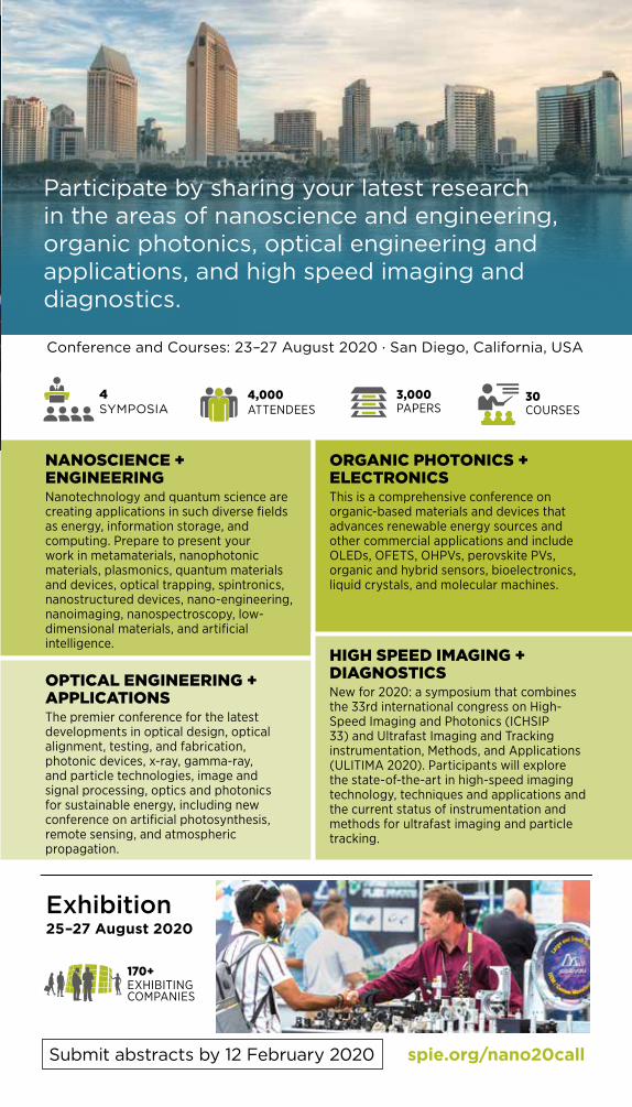
NANOSCIENCE + ENGINEERINGNanotechnology and quantum science are creating applications in such diverse fields as energy, information storage, and computing. Prepare to present your work in metamaterials, nanophotonic materials, plasmonics, quantum materials and devices, optical trapping, spintronics, nanostructured devices, nano-engineering, nanoimaging, nanospectroscopy, low-dimensional materials, and artificial intelligence.
ORGANIC PHOTONICS + ELECTRONICSThis is a comprehensive conference on organic-based materials and devices that advances renewable energy sources and other commercial applications and include OLEDs, OFETS, OHPVs, perovskite PVs, organic and hybrid sensors, bioelectronics, liquid crystals, and molecular machines.
OPTICAL ENGINEERING + APPLICATIONSThe premier conference for the latest developments in optical design, optical alignment, testing, and fabrication, photonic devices, x-ray, gamma-ray, and particle technologies, image and signal processing, optics and photonics for sustainable energy, including new conference on artificial photosynthesis, remote sensing, and atmospheric propagation.
HIGH SPEED IMAGING + DIAGNOSTICSNew for 2020: a symposium that combines the 33rd international congress on High-Speed Imaging and Photonics (ICHSIP 33) and Ultrafast Imaging and Tracking instrumentation, Methods, and Applications (ULITIMA 2020). Participants will explore the state-of-the-art in high-speed imaging technology, techniques and applications and the current status of instrumentation and methods for ultrafast imaging and particle tracking.
Conference and Courses: 23–27 August 2020 · San Diego, California, USA
4,000 ATTENDEES
3,000 PAPERS
30 COURSES
4 SYMPOSIA
Exhibition 25–27 August 2020
170+ EXHIBITING COMPANIES
Submit abstracts by 12 February 2020 spie.org/nano20call
Participate by sharing your latest research in the areas of nanoscience and engineering, organic photonics, optical engineering and applications, and high speed imaging and diagnostics.
Conferences and Courses23–27 August 2020
Exhibition 25–27 August 2020
23–2
7 A
ugus
t 20
20S
an D
ieg
o C
onv
enti
on
Cen
ter
San
Die
go
, Cal
ifo
rnia
, US
A
Cal
l for
Pap
ers
Par
tici
pat
e in
the
pre
mie
r ev
ent
for
op
tica
l en
gin
eeri
ng a
nd a
pp
licat
ions
, nan
ote
chno
log
y,
qua
ntum
sci
ence
, org
anic
pho
toni
cs, a
nd h
igh
sp
eed
imag
ing
and
dia
gno
stic
s.
spie
.org
/nan
o20
call
Non-
Profi
t Org
.U.
S. P
osta
ge
Paid
SPIE
P.O
. Box
10Be
lling
ham
, WA
9822
7-00
10 U
SA