Embed Size (px)
Citation preview
MP6532 5V to 60V, Three-Phase Brushless
DC Motor Pre-Driver
MP6532 Rev. 1.23 www.MonolithicPower.com 1
8/9/2018 MPS Proprietary Information. Patent Protected. Unauthorized Photocopy and Duplication Prohibited. © 2018 MPS. All Rights Reserved.
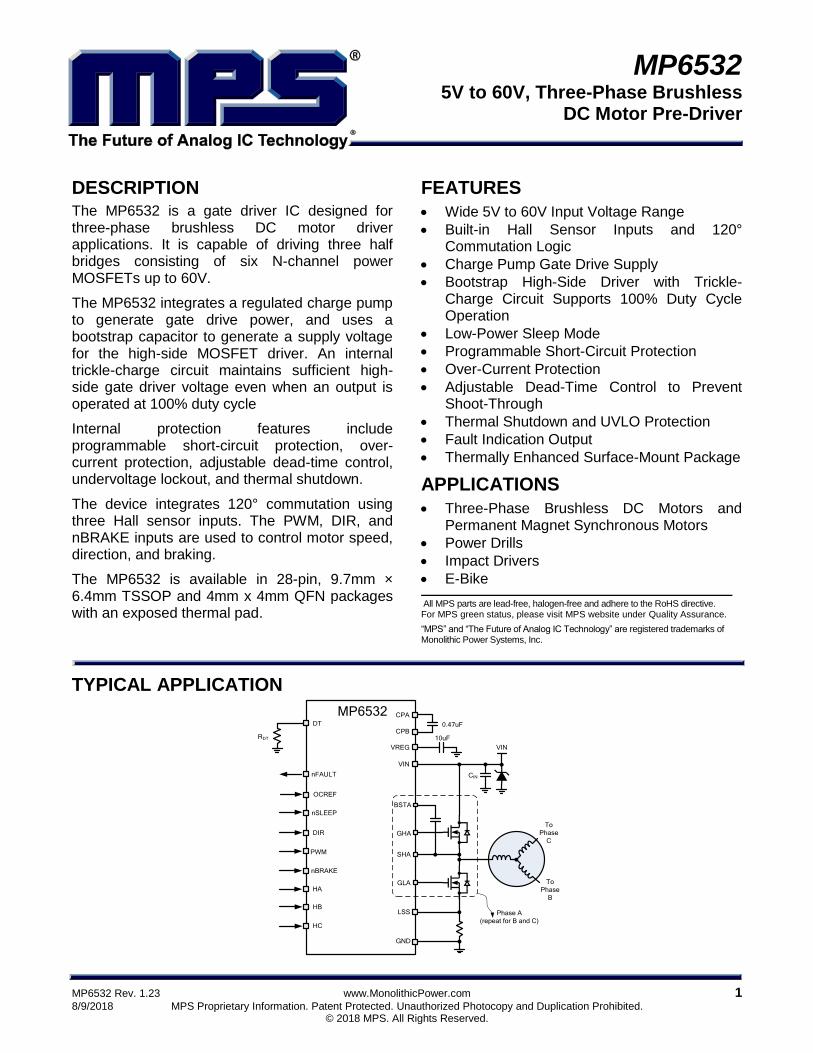
DESCRIPTION The MP6532 is a gate driver IC designed for three-phase brushless DC motor driver applications. It is capable of driving three half bridges consisting of six N-channel power MOSFETs up to 60V.
The MP6532 integrates a regulated charge pump to generate gate drive power, and uses a bootstrap capacitor to generate a supply voltage for the high-side MOSFET driver. An internal trickle-charge circuit maintains sufficient high-side gate driver voltage even when an output is operated at 100% duty cycle
Internal protection features include programmable short-circuit protection, over-current protection, adjustable dead-time control, undervoltage lockout, and thermal shutdown.
The device integrates 120° commutation using three Hall sensor inputs. The PWM, DIR, and nBRAKE inputs are used to control motor speed, direction, and braking.
The MP6532 is available in 28-pin, 9.7mm × 6.4mm TSSOP and 4mm x 4mm QFN packages with an exposed thermal pad.
FEATURES
Wide 5V to 60V Input Voltage Range
Built-in Hall Sensor Inputs and 120° Commutation Logic
Charge Pump Gate Drive Supply
Bootstrap High-Side Driver with Trickle-Charge Circuit Supports 100% Duty Cycle Operation
Low-Power Sleep Mode
Programmable Short-Circuit Protection
Over-Current Protection
Adjustable Dead-Time Control to Prevent Shoot-Through
Thermal Shutdown and UVLO Protection
Fault Indication Output
Thermally Enhanced Surface-Mount Package
APPLICATIONS
Three-Phase Brushless DC Motors and Permanent Magnet Synchronous Motors
Power Drills
Impact Drivers
E-Bike
All MPS parts are lead-free, halogen-free and adhere to the RoHS directive. For MPS green status, please visit MPS website under Quality Assurance.
“MPS” and “The Future of Analog IC Technology” are registered trademarks of Monolithic Power Systems, Inc.
TYPICAL APPLICATION
HA
HB
HC
OCREF
nFAULT
DT
MP6532
RDT
DIR
PWM
nBRAKE
nSLEEP
CPA
CPB
VREG
VIN
LSS
VIN
0.47uF
10uF
CIN
GLA
GHA
SHA
Phase A
(repeat for B and C)
To
Phase
B
To
Phase
C
GND
BSTA
MP6532 – 5V TO 60V, THREE PHASE BLDC MOTOR PRE-DRIVER
MP6532 Rev. 1.23 www.MonolithicPower.com 2
8/9/2018 MPS Proprietary Information. Patent Protected. Unauthorized Photocopy and Duplication Prohibited. © 2018 MPS. All Rights Reserved.
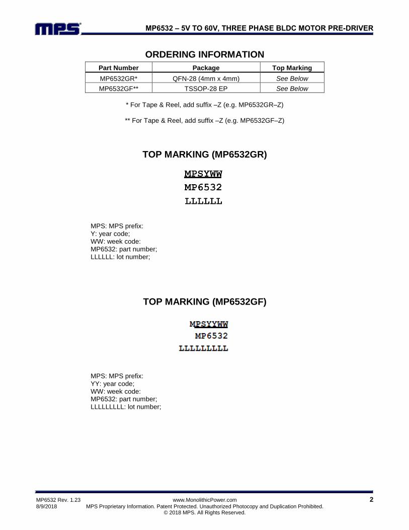
ORDERING INFORMATION
Part Number Package Top Marking
MP6532GR* QFN-28 (4mm x 4mm) See Below
MP6532GF** TSSOP-28 EP See Below
* For Tape & Reel, add suffix –Z (e.g. MP6532GR–Z)
** For Tape & Reel, add suffix –Z (e.g. MP6532GF–Z)
TOP MARKING (MP6532GR)
MPS: MPS prefix: Y: year code; WW: week code: MP6532: part number; LLLLLL: lot number;
TOP MARKING (MP6532GF)
MPS: MPS prefix: YY: year code; WW: week code: MP6532: part number; LLLLLLLLL: lot number;
MP6532 – 5V TO 60V, THREE PHASE BLDC MOTOR PRE-DRIVER
MP6532 Rev. 1.23 www.MonolithicPower.com 3
8/9/2018 MPS Proprietary Information. Patent Protected. Unauthorized Photocopy and Duplication Prohibited. © 2018 MPS. All Rights Reserved.
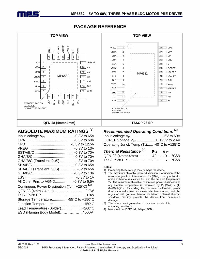
PACKAGE REFERENCE
ABSOLUTE MAXIMUM RATINGS (1) Input Voltage VIN ............................ -0.3V to 65V CPA ............................................... -0.3V to 60V CPB ............................................ -0.3V to 12.5V VREG ............................................ -0.3V to 13V BSTA/B/C ...................................... -0.3V to 70V GHA/B/C ........................................ -0.3V to 70V GHA/B/C (Transient, 2μS) ................ -8V to 70V SHA/B/C ........................................ -0.3V to 65V SHA/B/C (Transient, 2μS) ................. -8V to 65V GLA/B/C ........................................ -0.3V to 13V LSS .................................................. -0.3V to 1V All Other Pins to AGND ................. -0.3V to 6.5V
Continuous Power Dissipation (TA = +25°C) (2)
QFN-28 (4mm x 4mm)…………………… 2.9W TSSOP-28 EP ........................................... 3.9W
Storage Temperature ............... -55C to +150C
Junction Temperature ............................ +150C
Lead Temperature (Solder) .................... +260C ESD (Human Body Model)……………….1500V
Recommended Operating Conditions (3)
Input Voltage VIN ................................ 5V to 60V OCREF Voltage VOC ................... 0.125V to 2.4V
Operating Junct. Temp (TJ) ...... -40C to +125C
Thermal Resistance (4)
θJA θJC QFN-28 (4mm×4mm) ............. 42 ....... 9 .... °C/W TSSOP-28 EP ........................ 32 ....... 6 .... °C/W
Notes: 1) Exceeding these ratings may damage the device. 2) The maximum allowable power dissipation is a function of the
maximum junction temperature TJ (MAX), the junction-to-ambient thermal resistance θJA, and the ambient temperature TA. The maximum allowable continuous power dissipation at any ambient temperature is calculated by PD (MAX) = (TJ
(MAX)-TA)/θJA. Exceeding the maximum allowable power dissipation will cause excessive die temperature, and the regulator will go into thermal shutdown. Internal thermal shutdown circuitry protects the device from permanent damage.
3) The device is not guaranteed to function outside of its operating conditions.
4) Measured on JESD51-7, 4-layer PCB.
TOP VIEW TOP VIEW
1
VREG
EXPOSED PAD ON
BACKSIDE
CONNECTED TO GND
MP6532
2
3
4
5
6
7
28
27
26
25
24
23
22
21
20
19
18
17
16
15
14
13
12
11
1098
BSTA
SHA
GHA
GL
A
BS
TB
SH
B
GH
B
GL
B
BS
TC
SH
C
GHC
GLC
LSS
DIR
PW
M
DT
HA
HB
HC
VIN
CPA
CPB
GN
D
nBRAKE
OC
RE
F
nS
LE
EP
nF
AU
LT
HB
GND
DIR
PWM
HCLSS
CPB
SHB
BSTC
1
2
3
4
5
6
7
8
9
10
11
12
13
14
28
27
26
25
24
23
22
21
20
19
18
17
16
15
MP6532
CPA
VREG
SHC
BSTB
SHA
BSTA
GHB
VIN
nSLEEP
nBRAKE
DT
OCREF
nFAULT
HA
EXPOSED PAD ON
BACKSIDE
CONNECTED TO GND
GLA
GLB
GHA
GHC
GLC
QFN-28 (4mm×4mm) TSSOP-28 EP
MP6532 – 5V TO 60V, THREE PHASE BLDC MOTOR PRE-DRIVER
MP6532 Rev. 1.23 www.MonolithicPower.com 4
8/9/2018 MPS Proprietary Information. Patent Protected. Unauthorized Photocopy and Duplication Prohibited. © 2018 MPS. All Rights Reserved.
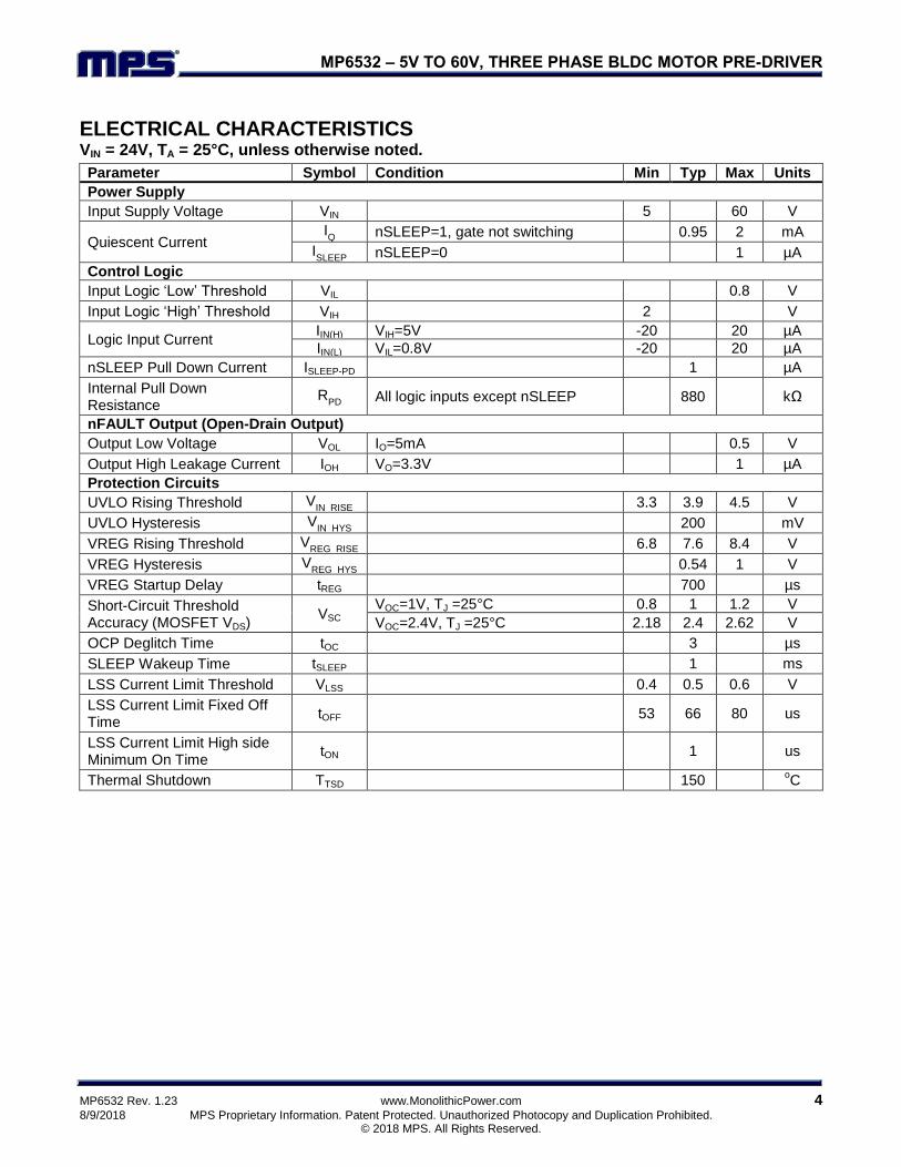
ELECTRICAL CHARACTERISTICS VIN = 24V, TA = 25°C, unless otherwise noted.
Parameter Symbol Condition Min Typ Max Units
Power Supply
Input Supply Voltage VIN 5 60 V
Quiescent Current IQ nSLEEP=1, gate not switching 0.95 2 mA
ISLEEP
nSLEEP=0 1 µA
Control Logic
Input Logic ‘Low’ Threshold VIL 0.8 V
Input Logic ‘High’ Threshold VIH 2 V
Logic Input Current IIN(H) VIH=5V -20 20 µA
IIN(L) VIL=0.8V -20 20 µA
nSLEEP Pull Down Current ISLEEP-PD 1 µA
Internal Pull Down Resistance
RPD
All logic inputs except nSLEEP 880 kΩ
nFAULT Output (Open-Drain Output)
Output Low Voltage VOL IO=5mA 0.5 V
Output High Leakage Current IOH VO=3.3V 1 µA
Protection Circuits
UVLO Rising Threshold VIN_RISE
3.3 3.9 4.5 V
UVLO Hysteresis VIN_HYS
200 mV
VREG Rising Threshold VREG_RISE
6.8 7.6 8.4 V
VREG Hysteresis VREG_HYS
0.54 1 V
VREG Startup Delay tREG 700 µs
Short-Circuit Threshold Accuracy (MOSFET VDS)
VSC VOC=1V, TJ =25°C 0.8 1 1.2 V
VOC=2.4V, TJ =25°C 2.18 2.4 2.62 V
OCP Deglitch Time tOC 3 µs
SLEEP Wakeup Time tSLEEP 1 ms
LSS Current Limit Threshold VLSS 0.4 0.5 0.6 V
LSS Current Limit Fixed Off Time
tOFF 53 66 80 us
LSS Current Limit High side Minimum On Time
tON 1 us
Thermal Shutdown TTSD 150 oC
MP6532 – 5V TO 60V, THREE PHASE BLDC MOTOR PRE-DRIVER
MP6532 Rev. 1.23 www.MonolithicPower.com 5
8/9/2018 MPS Proprietary Information. Patent Protected. Unauthorized Photocopy and Duplication Prohibited. © 2018 MPS. All Rights Reserved.
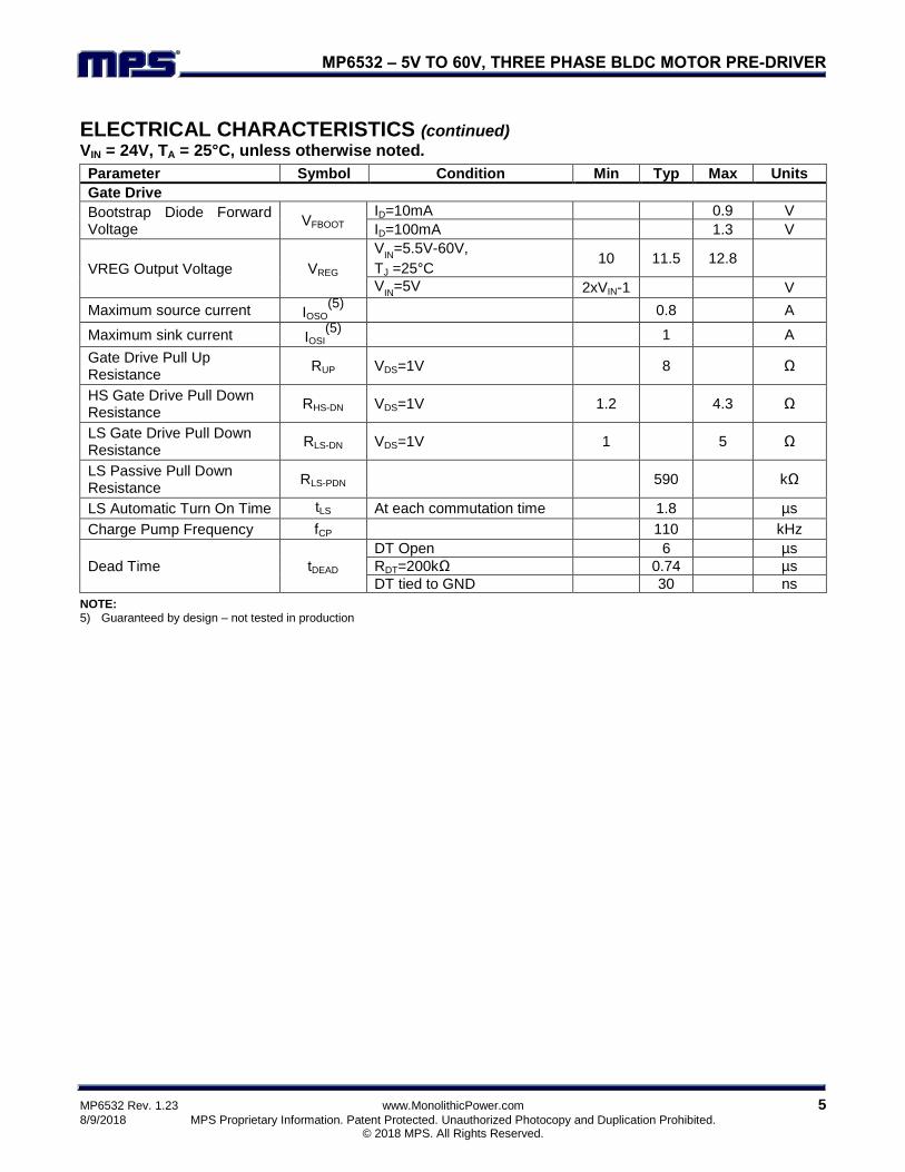
ELECTRICAL CHARACTERISTICS (continued) VIN = 24V, TA = 25°C, unless otherwise noted.
Parameter Symbol Condition Min Typ Max Units
Gate Drive
Bootstrap Diode Forward Voltage
VFBOOT ID=10mA 0.9 V
ID=100mA 1.3 V
VREG Output Voltage VREG
VIN
=5.5V-60V,
TJ =25°C 10 11.5 12.8
VIN
=5V 2xVIN-1 V
Maximum source current IOSO
(5) 0.8 A
Maximum sink current IOSI
(5) 1 A
Gate Drive Pull Up Resistance
RUP VDS=1V 8 Ω
HS Gate Drive Pull Down Resistance
RHS-DN VDS=1V 1.2 4.3 Ω
LS Gate Drive Pull Down Resistance
RLS-DN VDS=1V 1 5 Ω
LS Passive Pull Down Resistance
RLS-PDN 590 kΩ
LS Automatic Turn On Time tLS At each commutation time 1.8 µs
Charge Pump Frequency fCP 110 kHz
Dead Time tDEAD
DT Open 6 µs
RDT=200kΩ 0.74 µs
DT tied to GND 30 ns
NOTE: 5) Guaranteed by design – not tested in production
MP6532 – 5V TO 60V, THREE PHASE BLDC MOTOR PRE-DRIVER
MP6532 Rev. 1.23 www.MonolithicPower.com 6
8/9/2018 MPS Proprietary Information. Patent Protected. Unauthorized Photocopy and Duplication Prohibited. © 2018 MPS. All Rights Reserved.
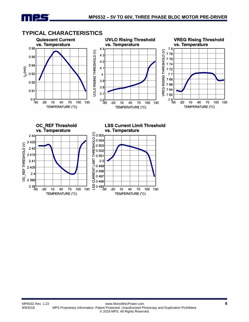
TYPICAL CHARACTERISTICS
MP6532 – 5V TO 60V, THREE PHASE BLDC MOTOR PRE-DRIVER
MP6532 Rev. 1.23 www.MonolithicPower.com 7
8/9/2018 MPS Proprietary Information. Patent Protected. Unauthorized Photocopy and Duplication Prohibited. © 2018 MPS. All Rights Reserved.
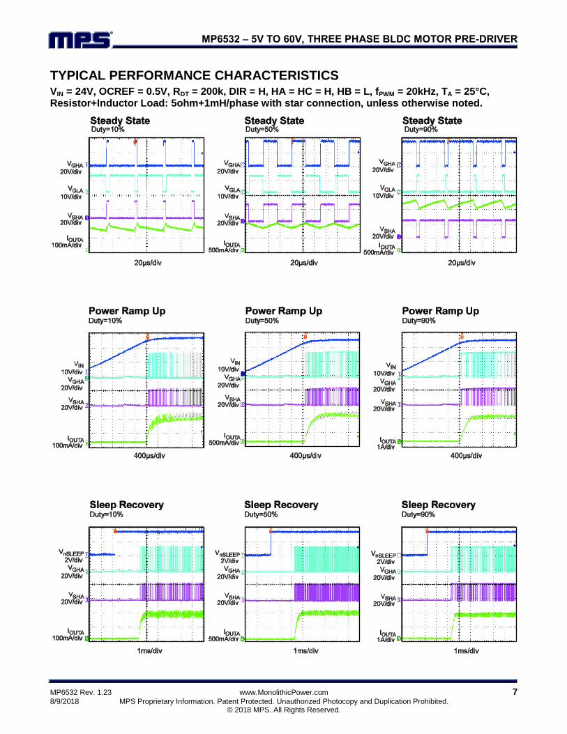
TYPICAL PERFORMANCE CHARACTERISTICS VIN = 24V, OCREF = 0.5V, RDT = 200k, DIR = H, HA = HC = H, HB = L, fPWM = 20kHz, TA = 25°C, Resistor+Inductor Load: 5ohm+1mH/phase with star connection, unless otherwise noted.
MP6532 – 5V TO 60V, THREE PHASE BLDC MOTOR PRE-DRIVER
MP6532 Rev. 1.23 www.MonolithicPower.com 8
8/9/2018 MPS Proprietary Information. Patent Protected. Unauthorized Photocopy and Duplication Prohibited. © 2018 MPS. All Rights Reserved.
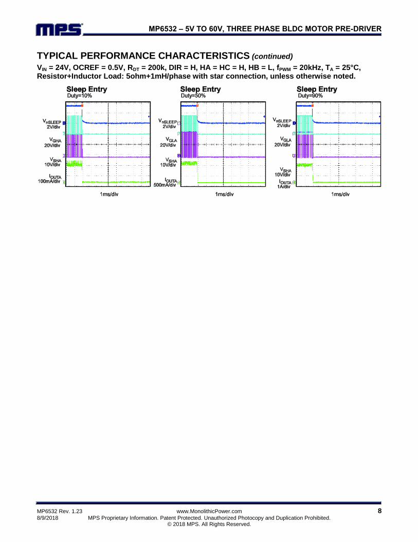
TYPICAL PERFORMANCE CHARACTERISTICS (continued) VIN = 24V, OCREF = 0.5V, RDT = 200k, DIR = H, HA = HC = H, HB = L, fPWM = 20kHz, TA = 25°C, Resistor+Inductor Load: 5ohm+1mH/phase with star connection, unless otherwise noted.
MP6532 – 5V TO 60V, THREE PHASE BLDC MOTOR PRE-DRIVER
MP6532 Rev. 1.23 www.MonolithicPower.com 9
8/9/2018 MPS Proprietary Information. Patent Protected. Unauthorized Photocopy and Duplication Prohibited. © 2018 MPS. All Rights Reserved.
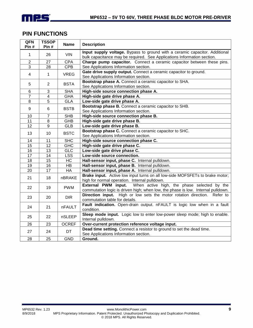
PIN FUNCTIONS
QFN Pin #
TSSOP Pin #
Name Description
1 26 VIN Input supply voltage. Bypass to ground with a ceramic capacitor. Additional bulk capacitance may be required. See Applications Information section.
2 27 CPA Charge pump capacitor. Connect a ceramic capacitor between these pins. See Applications Information section. 3 28 CPB
4 1 VREG Gate drive supply output. Connect a ceramic capacitor to ground. See Applications Information section.
5 2 BSTA Bootstrap phase A. Connect a ceramic capacitor to SHA. See Applications Information section.
6 3 SHA High-side source connection phase A.
7 4 GHA High-side gate drive phase A.
8 5 GLA Low-side gate drive phase A.
9 6 BSTB Bootstrap phase B. Connect a ceramic capacitor to SHB. See Applications Information section.
10 7 SHB High-side source connection phase B.
11 8 GHB High-side gate drive phase B.
12 9 GLB Low-side gate drive phase B.
13 10 BSTC Bootstrap phase C. Connect a ceramic capacitor to SHC. See Applications Information section.
14 11 SHC High-side source connection phase C.
15 12 GHC High-side gate drive phase C.
16 13 GLC Low-side gate drive phase C.
17 14 LSS Low-side source connection.
18 15 HC Hall-sensor input, phase C. Internal pulldown.
19 16 HB Hall-sensor input, phase B. Internal pulldown.
20 17 HA Hall-sensor input, phase A. Internal pulldown.
21 18 nBRAKE Brake input. Active low input turns on all low-side MOFSFETs to brake motor; high for normal operation. Internal pulldown.
22 19 PWM External PWM input. When active high, the phase selected by the commutation logic is driven high; when low, the phase is low. Internal pulldown.
23 20 DIR Direction input. High or low sets the motor rotation direction. Refer to commutation table for details.
24 21 nFAULT Fault indication. Open-drain output. nFAULT is logic low when in a fault condition.
25 22 nSLEEP Sleep mode input. Logic low to enter low-power sleep mode; high to enable. Internal pulldown.
26 23 OCREF Over-current protection reference voltage input.
27 24 DT Dead time setting. Connect a resistor to ground to set the dead time. See Applications Information section.
28 25 GND Ground.
MP6532 – 5V TO 60V, THREE PHASE BLDC MOTOR PRE-DRIVER
MP6532 Rev. 1.23 www.MonolithicPower.com 10
8/9/2018 MPS Proprietary Information. Patent Protected. Unauthorized Photocopy and Duplication Prohibited. © 2018 MPS. All Rights Reserved.
BLOCK DIAGRAM
PWM
DIR
nSLEEP
HA
nBRAKE
HC
HB
Charge
Pump
VIN
RSENSE
SHA
GND
Fault
Handling
SC
Comparator
Timing and
Control
Logic
DT
CPA CPB
VIN
VREG
GHA
GLA
HS Gate
Drive
LS Gate
Drive
Trickle
Charge
Phase A,
repeat for
B&C
LSS
nFAULT
RDT
BSTA
VREG
TSD
OCREF
VDS
Monitor
0.5VOCP
Comparator
UVLO
VIN
VIN
VREG
Figure 1: Functional Block Diagram
MP6532 – 5V TO 60V, THREE PHASE BLDC MOTOR PRE-DRIVER
MP6532 Rev. 1.23 www.MonolithicPower.com 11
8/9/2018 MPS Proprietary Information. Patent Protected. Unauthorized Photocopy and Duplication Prohibited. © 2018 MPS. All Rights Reserved.
OPERATION The MP6532 is a three-phase BLDC motor pre-driver with built-in commutation logic that drives three external N-channel MOSFET half bridges, with 0.8A source and 1A sink current capability. It operates over a wide input voltage range of 5V to 60V, generating a boosted gate drive voltage when the input supply is below 12V. The MP6532 features a low-power sleep mode, which disables the device and draws a very low supply current.
The MP6532 provides several flexible functions, such as adjustable dead-time control and over-current protection, which allow the device to cover a wide range of applications.
Power-Up Sequence The power-up sequence is initiated by the application of voltage to VIN pin. To initiate power-up, VIN must be above the undervoltage lockout threshold VUVLO.
After power-up begins, the VREG supply starts operating. VREG must rise above V
REG_RISE before the device becomes functional.
The power-up process takes between 1mS and 2mS, after which the MP6532 will respond to logic inputs and drive the outputs.
Gate Drive Power Supplies Gate drive voltages are generated from the input power, VIN. A regulated charge pump doubler circuit supplies a voltage of approximately 11.5V at the VREG pin. This voltage is used for the low-side gate drive supply. The charge pump requires external capacitors between the CPA and CPB pins, and from VREG to ground.
The high side gate drive is generated by a combination of a bootstrap capacitor and an internal “trickle” charge pump. Bootstrap capacitors are charged to the VREG voltage when the low side MOSFET is turned on. This charge is then used to drive the high side MOSFET gate when it is turned on.
To keep the bootstrap capacitors charged and allow operation at 100% duty cycle, an internal “trickle” charge pump supplies a small current (about 5µA) to overcome leakages that would discharge the bootstrap capacitors.
Refer to the applications information section for details on the selection of external components.
Sleep Mode (nSLEEP Input) Driving nSLEEP low will put the device into a low-power sleep state. In this state, all the internal circuits are disabled. All inputs are ignored when nSLEEP is active low. nSLEEP has an interval pulldown, so it must be driven high for the device to operate.
When exiting sleep mode, the power-up sequence described above is repeated.
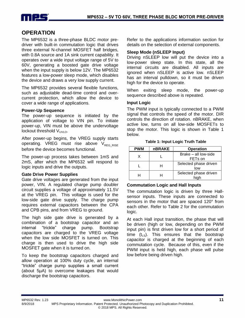
Input Logic
The PWM input is typically connected to a PWM signal that controls the speed of the motor. DIR controls the direction of rotation. nBRAKE, when active low, turns on all low-side MOSFETs to stop the motor. This logic is shown in Table 1 below.
Table 1: Input Logic Truth Table
PWM nBRAKE Operation
X L Brake – all low-side
FETs on
L H Selected phase driven
low
H H Selected phase driven
high
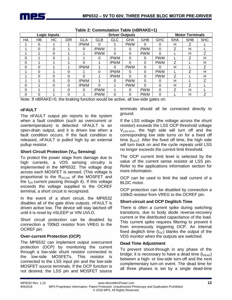
Commutation Logic and Hall Inputs
The commutation logic is driven by three Hall-sensor inputs. These inputs are connected to sensors in the motor that are spaced 120° from each other. Refer to Table 2 for the commutation logic.
At each Hall input transition, the phase that will be driven (high or low, depending on the PWM input pin) is first driven low for a short period of time (tLS). This ensures that the bootstrap capacitor is charged at the beginning of each commutation cycle. Because of this, even if the PWM input is held high, each phase will pulse low before being driven high.
MP6532 – 5V TO 60V, THREE PHASE BLDC MOTOR PRE-DRIVER
MP6532 Rev. 1.23 www.MonolithicPower.com 12
8/9/2018 MPS Proprietary Information. Patent Protected. Unauthorized Photocopy and Duplication Prohibited. © 2018 MPS. All Rights Reserved.
Table 2: Commutation Table (nBRAKE=1) Logic Inputs Driver Outputs Motor Terminals
HA HB HC DIR GLA GLB GLC GHA GHB GHC SHA SHB SHC
1 0 1 1 /PWM 0 1 PWM 0 0 H Z L
1 0 0 1 0 /PWM 1 0 PWM 0 Z H L
1 1 0 1 1 /PWM 0 0 PWM 0 L H Z
0 1 0 1 1 0 /PWM 0 0 PWM L Z H
0 1 1 1 0 1 /PWM 0 0 PWM Z L H
0 0 1 1 /PWM 1 0 PWM 0 0 H L Z
1 0 1 0 1 0 /PWM 0 0 PWM L Z H
1 0 0 0 0 1 /PWM 0 0 PWM Z L H
1 1 0 0 /PWM 1 0 PWM 0 0 H L Z
0 1 0 0 /PWM 0 1 PWM 0 0 H Z L
0 1 1 0 0 /PWM 1 0 PWM 0 Z H L
0 0 1 0 1 /PWM 0 0 PWM 0 L H Z
Note: If nBRAKE=0, the braking function would be active, all low-side gates on.
nFAULT
The nFAULT output pin reports to the system when a fault condition (such as overcurrent or overtemperature) is detected. nFAULT is an open-drain output, and it is driven low when a fault condition occurs. If the fault condition is released, nFAULT is pulled high by an external pullup resistor.
Short Circuit Protection (VDS Sensing)
To protect the power stage from damage due to high currents, a VDS sensing circuitry is implemented in the MP6532. The voltage drop across each MOSFET is sensed. (This voltage is proportional to the RDS-ON of the MOSFET and the IDS current passing through it). If this voltage exceeds the voltage supplied to the OCREF terminal, a short circuit is recognized.
In the event of a short circuit, the MP6532 disables all of the gate drive outputs. nFAULT is driven active low. The device will stay latched off until it is reset by nSLEEP or VIN UVLO.
Short circuit protection can be disabled by connection a 100kΩ resistor from VREG to the OCREF pin.
Over-current Protection (OCP)
The MP6532 can implement output overcurrent protection (OCP) by monitoring the current through a low-side shunt resistor connected to the low-side MOSFETs. This resistor is connected to the LSS input pin and the low-side MOSFET source terminals. If the OCP function is not desired, the LSS pin and MOSFET source
terminals should all be connected directly to ground.
If the LSS voltage (the voltage across the shunt resistor) exceeds the LSS OCP threshold voltage VLSS-OCP, the high side will turn off and the corresponding low side turns on for a fixed off time (tOFF). After the fixed off time, the high side will turn back on and the cycle repeats until LSS no longer exceeds the current limit threshold.
The OCP current limit level is selected by the value of the current sense resistor at LSS pin. Refer to the applications information section for more information.
OCP can be used to limit the stall current of a BLDC motor.
OCP protection can be disabled by connection a 100kΩ resistor from VREG to the OCREF pin.
Short-circuit and OCP Deglitch Time
There is often a current spike during switching transitions, due to body diode reverse-recovery current or the distributed capacitance of the load. This current spike requires filtering to prevent it from erroneously triggering OCP. An internal fixed deglitch time (tOC) blanks the output of the VDS monitor when the outputs are switched.
Dead Time Adjustment
To prevent shoot-through in any phase of the bridge, it is necessary to have a dead time (tDEAD) between a high- or low-side turn-off and the next complementary turn-on event. The dead time for all three phases is set by a single dead-time
MP6532 – 5V TO 60V, THREE PHASE BLDC MOTOR PRE-DRIVER
MP6532 Rev. 1.23 www.MonolithicPower.com 13
8/9/2018 MPS Proprietary Information. Patent Protected. Unauthorized Photocopy and Duplication Prohibited. © 2018 MPS. All Rights Reserved.
resistor (RDT) between DT and ground with Equation (1): tDEAD(nS) = 3.7*R(kΩ) (1)
If DT is tied directly to ground, an internal minimum dead time (30ns) will be applied. Leaving DT open generates approximately a 6µs dead time.
UVLO Protection
If at any time the voltage on VIN falls below the undervoltage lockout threshold VIN_RISE, all circuitry in the device is disabled and the internal logic will be reset.
Operation will resume with the power-up sequence when VIN rises above the UVLO thresholds.
After power-up, if the voltage on VREG drops below the V
REG_RISE threshold, the MP6530 will
enter a latched fault state and disable all functions. The nFAULT pin will be driven active low. The device will stay latched off until it is reset by nSLEEP or VIN UVLO.
Thermal Shutdown
If the die temperature exceeds safe limits, the MP6532 will enter a latched fault state and disable all functions. The device will stay latched off until it is reset by nSLEEP or UVLO.
MP6532 – 5V TO 60V, THREE PHASE BLDC MOTOR PRE-DRIVER
MP6532 Rev. 1.23 www.MonolithicPower.com 14
8/9/2018 MPS Proprietary Information. Patent Protected. Unauthorized Photocopy and Duplication Prohibited. © 2018 MPS. All Rights Reserved.
APPLICATIONS INFORMATION VIN Input Voltage
The VIN pin supplies all power to the device. It must be properly bypassed with a capacitor to ground – see below for specific recommendations.
The normal operating range of VIN is between 5V and 60V.
VIN should never be allowed to exceed the absolute maximum ratings, even in a short term transient condition, or damage to the device may result. In some cases – especially where mechanical energy can turn a motor into a generator – it may be necessary to use some form of overvoltage protection, such as a TVS diode, between VIN and ground.
Component Selection
MOSFET selection
Correctly selecting the power MOSFETs used to drive a motor is crucial to designing a successful motor drive.
The first requirement is that the MOSFET must have a VDS breakdown voltage that is higher than the supply voltage. It is recommended that considerable margin – 10-15 volts - be added to prevent MOSFET damage from transient voltages that can be caused by parasitic inductances in the PCB layout and wiring. For example, for 24V power supply applications, MOSFETs having a breakdown voltage of 40V-60V minimum are recommended. More margin is desirable in high current applications, as the transients caused by parasitic inductances may be larger. Also, there are conditions like regenerative braking that can inject current back into the power supply; care must be taken that this does not cause an increase in the power supply voltage large enough to damage components.
The MOSFETs must be able to safely pass the current needed to run the motor. The highest current condition, which is normally when the motor is first started or stalled, needs to be supported. This is typically called the “stall current” of the motor.
Related to the current capability of the MOSFET is the rds(on). This is the resistance of the MOSFET when it is in the fully “turned on” state. The MOSFET will dissipate power proportional to the rds(on) and the motor current: P=I2R. The rds(on) needs to be selected so that for the desired motor current, the heat generated in this power can be safely dissipated. In some cases, this may require special PCB design considerations and/or external heatsinks to be used for the MOSFETs.
Some consideration should be made for the safe operating area (SOA) of the MOSFETs in fault conditions, such as a short circuit. The IC will act quickly in the event of a short, but there is still a very short time (on the order of 3µS) where large currents can flow in the MOSFETs while the protection circuits recognize the fault and disable the outputs.
External Capacitor Selection
The MP6532 has a unique feature in that it can provide a gate drive voltage (VREG) of 10-12V even if the input supply voltage drops as low as 5V. This gate drive voltage is generated by a charge pump inside the part, which uses external capacitors.
The charge pump flying capacitor, CCP, should have a capacitance of 470nF. It needs to be rated to withstand the maximum VIN power supply voltage. An X7R or X5R ceramic capacitor is recommended. With a 470nF capacitor, VREG can output approximately 10mA when VIN is 5V. If operation below 10V is not needed, a 220nF capacitor can be used
To provide the large peak currents needed to turn on the HS MOSFET, bootstrap capacitors are used. These capacitors are charged when the output is driven low, then the charge in the bootstrap capacitor is used to turn on the HS MOSFET when the output is driven high. (Note that an internal charge pump will keep the bootstrap capacitor changed when the output is held high for an extended period).
The bootstrap capacitors are selected depending on the MOSFET total gate charge. When the HS MOSFET is turned on, the charge stored in the
MP6532 – 5V TO 60V, THREE PHASE BLDC MOTOR PRE-DRIVER
MP6532 Rev. 1.23 www.MonolithicPower.com 15
8/9/2018 MPS Proprietary Information. Patent Protected. Unauthorized Photocopy and Duplication Prohibited. © 2018 MPS. All Rights Reserved.
bootstrap capacitor is transferred to the HS MOSFET gate. As a simplified approximation, the minimum bootstrap capacitance can be estimated as CBOOT > 8*QG, where QG is the total gate charge of the MOSFET in nC, and CBOOT is in nF. The bootstrap capacitors should not exceed 1µF, or they may cause improper operation at start-up.
For most applications, bootstrap capacitors between 0.1µF and 1µF, X5R or X7R ceramic, rated for 25V minimum, are recommended.
The VREG pin requires a bypass capacitor to ground of 10µF. This should be an X7R or X5R ceramic capacitor rated for 16V minimum.
VIN requires a bypass capacitor to ground, placed as close as possible to the device. At a minimum, a 0.1µF X5R or X7R ceramic capacitor, rated for the VIN voltage, is recommended.
Depending on the power supply impedance and the distance between the MOSFETs and the power supply, additional bulk capacitance is usually needed. Between 47µF and 470µF of low ESR electrolytic capacitors are typically used.
Dead Time Resistor Selection
During the transition between driving an output low and high, there is a short period when neither the HS nor LS MOSFET is turned on. This period, called “dead time”, is needed to prevent any overlap in conduction between HS and LS MOSFETs, which would effectively provide a short-circuit directly between the power supply and ground. This condition, referred to as “shoot-through”, causes large transient currents, and can destroy the MOSFETs.
Since motors are inductive by nature, once current is flowing in the motor, it cannot stop immediately, even if the MOSFETs are turned off. This “recirculation current” continues to flow in the original direction until the magnetic field has decayed.
When the MOSFETs are turned off, this current will flow through the “body diode” which is inherent in the MOSFET device.
MOSFET body diodes have a much higher voltage drop than the MOSFET has during conduction, so there more power dissipated in body diode conduction than during the on time.
Because of this, it is desirable to minimize the dead time. However, the dead time must be made large enough to guarantee under all conditions that the HS and LS MOSFETs are never turned on at the same time.
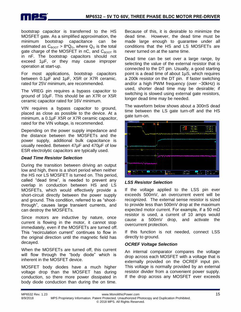
Dead time can be set over a large range, by selecting the value of the external resistor that is connected to the DT pin. Usually, a good starting point is a dead time of about 1µS, which requires a 200k resistor on the DT pin. If faster switching and/or a high PWM frequency (over ~30kHz) is used, shorter dead time may be desirable; if switching is slowed using external gate resistors, longer dead time may be needed.
The waveform below shows about a 300nS dead time between the LS gate turn-off and the HS gate turn-on.
LSS Resistor Selection
If the voltage applied to the LSS pin ever exceeds 500mV, an overcurrent event will be recognized. The external sense resistor is sized to provide less than 500mV drop at the maximum expected motor current. For example, if a 50 mΩ resistor is used, a current of 10 amps would cause a 500mV drop, and activate the overcurrent protection.
If this function is not needed, connect LSS directly to ground.
OCREF Voltage Selection
An internal comparator compares the voltage drop across each MOSFET with a voltage that is externally provided on the OCREF input pin. This voltage is normally provided by an external resistor divider from a convenient power supply. If the drop across any MOSFET ever exceeds
MP6532 – 5V TO 60V, THREE PHASE BLDC MOTOR PRE-DRIVER
MP6532 Rev. 1.23 www.MonolithicPower.com 16
8/9/2018 MPS Proprietary Information. Patent Protected. Unauthorized Photocopy and Duplication Prohibited. © 2018 MPS. All Rights Reserved.
the voltage on the OCREF pin, a short-circuit event is recognized.
If this function is not needed, connect OCREF to VREG through a 100k resistor.
Gate Drive Considerations
The gate characteristics of the selected MOSFETs will affect how fast they will be switched and off. The gate drive outputs of the device can be connected directly to the gates of the power MOSFETs, which results in the fastest possible turn-on and turn-off times. However, it may be advantageous to add external components (resistors and/or diodes) to modify the MOSFET turn-on and turn-off characteristics.
Adding external series resistance – typically between 10 and 100 ohms – will limit the current that charges and discharges the gate of the MOSFET, which will slow down the turn-on and turn-off times. Sometimes this is desirable to control EMI and noise. Slowing the transition down too much, however, results in large power dissipation in the MOSFET during switching.
In some cases, it is desirable to have a slow turn-on, but a fast turn-off. This can be implemented by using a series resistor in parallel with a diode. At turn-on, the resistor limits the current flow into the gate; at turn-off, the gate is discharged quickly through the diode.
RGHS
RGLS
1N4148
1N4148
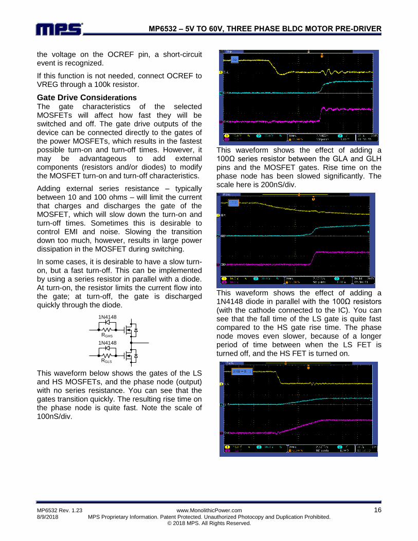
This waveform below shows the gates of the LS and HS MOSFETs, and the phase node (output) with no series resistance. You can see that the gates transition quickly. The resulting rise time on the phase node is quite fast. Note the scale of 100nS/div.
This waveform shows the effect of adding a 100Ω series resistor between the GLA and GLH pins and the MOSFET gates. Rise time on the phase node has been slowed significantly. The scale here is 200nS/div.
This waveform shows the effect of adding a 1N4148 diode in parallel with the 100Ω resistors (with the cathode connected to the IC). You can see that the fall time of the LS gate is quite fast compared to the HS gate rise time. The phase node moves even slower, because of a longer period of time between when the LS FET is turned off, and the HS FET is turned on.
MP6532 – 5V TO 60V, THREE PHASE BLDC MOTOR PRE-DRIVER
MP6532 Rev. 1.23 www.MonolithicPower.com 17
8/9/2018 MPS Proprietary Information. Patent Protected. Unauthorized Photocopy and Duplication Prohibited. © 2018 MPS. All Rights Reserved.
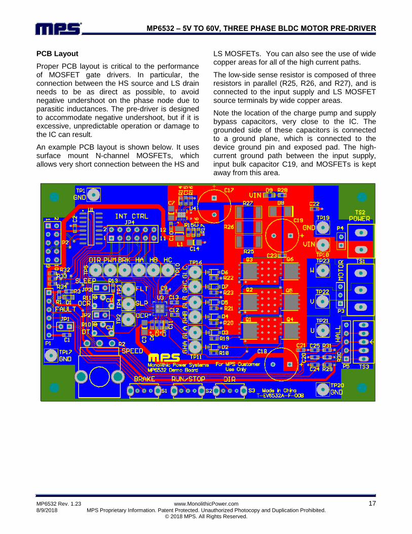
PCB Layout
Proper PCB layout is critical to the performance of MOSFET gate drivers. In particular, the connection between the HS source and LS drain needs to be as direct as possible, to avoid negative undershoot on the phase node due to parasitic inductances. The pre-driver is designed to accommodate negative undershoot, but if it is excessive, unpredictable operation or damage to the IC can result.
An example PCB layout is shown below. It uses surface mount N-channel MOSFETs, which allows very short connection between the HS and
LS MOSFETs. You can also see the use of wide copper areas for all of the high current paths.
The low-side sense resistor is composed of three resistors in parallel (R25, R26, and R27), and is connected to the input supply and LS MOSFET source terminals by wide copper areas.
Note the location of the charge pump and supply bypass capacitors, very close to the IC. The grounded side of these capacitors is connected to a ground plane, which is connected to the device ground pin and exposed pad. The high-current ground path between the input supply, input bulk capacitor C19, and MOSFETs is kept away from this area.
MP6532 – 5V TO 60V, THREE PHASE BLDC MOTOR PRE-DRIVER
MP6532 Rev. 1.23 www.MonolithicPower.com 18
8/9/2018 MPS Proprietary Information. Patent Protected. Unauthorized Photocopy and Duplication Prohibited. © 2018 MPS. All Rights Reserved.
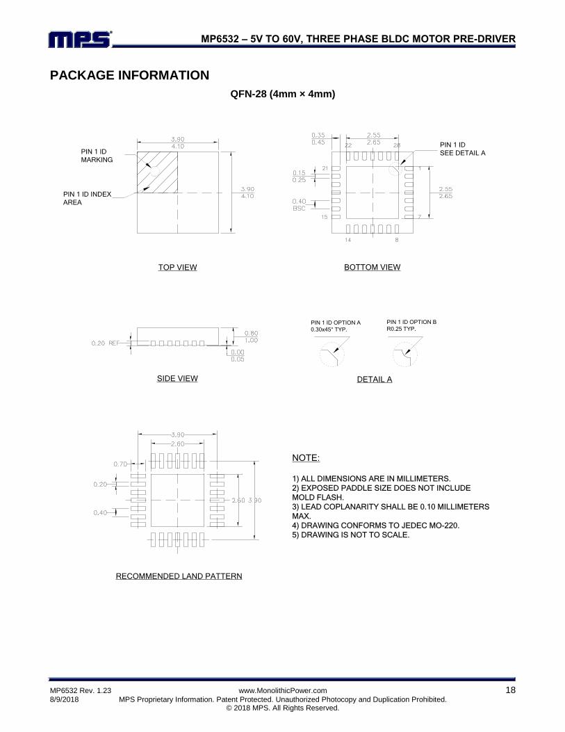
PACKAGE INFORMATION
QFN-28 (4mm × 4mm)
SIDE VIEW
BOTTOM VIEW
NOTE:
1) ALL DIMENSIONS ARE IN MILLIMETERS.
2) EXPOSED PADDLE SIZE DOES NOT INCLUDE
MOLD FLASH.
3) LEAD COPLANARITY SHALL BE 0.10 MILLIMETERS
MAX.
4) DRAWING CONFORMS TO JEDEC MO-220.
5) DRAWING IS NOT TO SCALE.
PIN 1 ID
MARKING
TOP VIEW
PIN 1 ID INDEX
AREA
RECOMMENDED LAND PATTERN
PIN 1 ID
SEE DETAIL A
PIN 1 ID OPTION A
0.30x45° TYP.
PIN 1 ID OPTION B
R0.25 TYP.
DETAIL A
MP6532 – 5V TO 60V, THREE PHASE BLDC MOTOR PRE-DRIVER
NOTICE: The information in this document is subject to change without notice. Users should warrant and guarantee that third
party Intellectual Property rights are not infringed upon when integrating MPS products into any application. MPS will not assume any legal responsibility for any said applications.
MP6532 Rev. 1.23 www.MonolithicPower.com 19
8/9/2018 MPS Proprietary Information. Patent Protected. Unauthorized Photocopy and Duplication Prohibited. © 2018 MPS. All Rights Reserved.
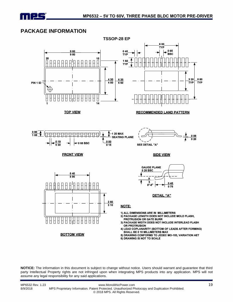
PACKAGE INFORMATION
TSSOP-28 EP


![Grief Resource List [rev 6.1.20] - rwjms.umdnj.edurwjms.umdnj.edu/departments_institutes/boggscenter/links/documen… · Y a G o t P e o p l e : H e l p i n g P e o p l e w i t h](https://img.pdfslide.us/doc/110x75/5f95c2d71360c973412fecd1/grief-resource-list-rev-6120-rwjmsumdnj-y-a-g-o-t-p-e-o-p-l-e-h-e-l-p.jpg)


![Grief Resource List [rev 6.1.20] · Y a G o t P e o p l e : H e l p i n g P e o p l e w i t h D e v e l o p m e n ta l D is a b i li tie s D e a l w i t h G r ie f , B e r e a v e](https://img.pdfslide.us/doc/110x75/5f47875c717b3b07ff122afd/grief-resource-list-rev-6120-y-a-g-o-t-p-e-o-p-l-e-h-e-l-p-i-n-g-p-e-o-p-l.jpg)


![P H I L L I P S · s t e p h e n p h i l l i p s # #s 1;7 j/ s#8 ;];a ; p r o f e s s i o n a l p r o f i l e g ¯¹£ / ¯|ÊÀ ; Æp£;7p¼ Æ ª ;]](https://img.pdfslide.us/doc/110x75/5ffc8c8fbb3ab65b6c6d0e14/p-h-i-l-l-i-p-s-s-t-e-p-h-e-n-p-h-i-l-l-i-p-s-s-17-j-s8-a-p-r-o-f-e-s.jpg)