Embed Size (px)
Citation preview
C141-E045-02EN
MPB3021ATMPB3032ATMPB3043ATMPB3052ATMPB3064AT
DISK DRIVES
PRODUCT MANUAL
C141-E045-02EN i
REVISION RECORD
Edition Date published Revised contents
01 August., 1997
02 March, 1998 All pages revised.
Specification No.: C141-E045-**EN
The contents of this manual is subject tochange without prior notice.
All Rights Reserved.Copyright 1998 FUJITSU LIMITED

C141-E045-02EN iii
PREFACE
This manual describes the MPB3021AT/MPB3032AT/MPB3043AT/MPB3052AT/MPB3064AT, a3.5-inch hard disk drive with a BUILT-IN controller that is compatible with the ATA interface.
This manual explains, in detail, how to incorporate the hard disk drives into user systems.
This manual assumes that users have a basic knowledge of hard disk drives and their application incomputer systems.
This manual consists of the following six chapters:
Chapter 1 DEVICE OVERVIEW
Chapter 2 DEVICE CONFIGURATION
Chapter 3 INSTALLATION CONDITIONS
Chapter 4 THEORY OF DEVICE OPERATION
Chapter 5 INTERFACE
Chapter 6 OPERATIONS
In this manual, disk drives may be referred to as drives or devices.
iv C141-E045-02EN
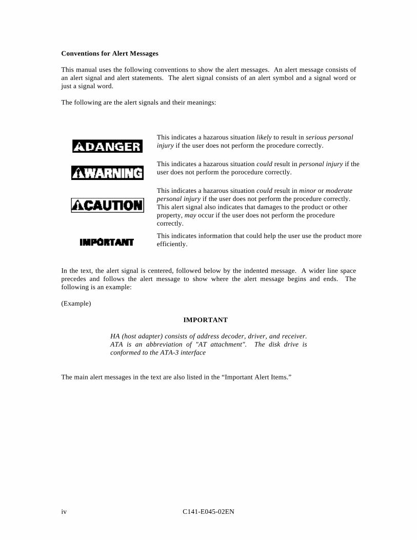
Conventions for Alert Messages
This manual uses the following conventions to show the alert messages. An alert message consists ofan alert signal and alert statements. The alert signal consists of an alert symbol and a signal word orjust a signal word.
The following are the alert signals and their meanings:
This indicates a hazarous situation likely to result in serious personalinjury if the user does not perform the procedure correctly.
This indicates a hazarous situation could result in personal injury if theuser does not perform the porocedure correctly.
This indicates a hazarous situation could result in minor or moderatepersonal injury if the user does not perform the procedure correctly.This alert signal also indicates that damages to the product or otherproperty, may occur if the user does not perform the procedurecorrectly.
This indicates information that could help the user use the product moreefficiently.
In the text, the alert signal is centered, followed below by the indented message. A wider line spaceprecedes and follows the alert message to show where the alert message begins and ends. Thefollowing is an example:
(Example)
IMPORTANT
HA (host adapter) consists of address decoder, driver, and receiver.ATA is an abbreviation of "AT attachment". The disk drive isconformed to the ATA-3 interface
The main alert messages in the text are also listed in the “Important Alert Items.”
C141-E045-02EN v
LIABILITY EXCEPTION
"Disk drive defects" refers to defects that involve adjustment, repair, or replacement.Fujitsu is not liable for any other disk drive defects, such as those caused by user misoperation ormishandling, inappropriate operating environments, defects in the power supply or cable, problems ofthe host system, or other causes outside the disk drive.

C141-E045-02EN vii
CONTENTS
page
CHAPTER 1 DEVICE OVERVIEW ................................................................................... 1 - 1
1.1 Features .......................................................................................................................... 1 - 1
1.1.1 Functions and performance ............................................................................................ 1 - 1
1.1.2 Adaptability.................................................................................................................... 1 - 2
1.1.3 Interface.......................................................................................................................... 1 - 2
1.2 Device Specifications ..................................................................................................... 1 - 4
1.2.1 Specifications summary.................................................................................................. 1 - 4
1.2.2 Model and product number ............................................................................................ 1 - 5
1.3 Power Requirements....................................................................................................... 1 - 5
1.4 Environmental Specifications......................................................................................... 1 - 8
1.5 Acoustic Noise ............................................................................................................... 1 - 8
1.6 Shock and Vibration....................................................................................................... 1 - 9
1.7 Reliability ....................................................................................................................... 1 - 9
1.8 Error Rate ....................................................................................................................... 1 - 10
1.9 Media Defects................................................................................................................. 1 - 10
CHAPTER 2 DEVICE CONFIGURATION ....................................................................... 2 - 1
2.1 Device Configuration ..................................................................................................... 2 - 1
2.2 System Configuration..................................................................................................... 2 - 4
2.2.1 ATA interface ................................................................................................................. 2 - 4
2.2.2 1 drive connection .......................................................................................................... 2 - 4
2.2.3 2 drives connection......................................................................................................... 2 - 5
CHAPTER 3 INSTALLATION CONDITIONS ................................................................. 3 - 1
3.1 Dimensions..................................................................................................................... 3 - 1
3.2 Mounting........................................................................................................................ 3 - 3
3.3 Cable Connections.......................................................................................................... 3 - 7
3.3.1 Device connector ............................................................................................................ 3 - 7
3.3.2 Cable connector specifications ....................................................................................... 3 - 8
3.3.3 Device connection .......................................................................................................... 3 - 8
3.3.4 Power supply connector (CN1) ...................................................................................... 3 - 9
3.4 Jumper Settings .............................................................................................................. 3 - 9
C141-E045-02ENviii
3.4.1 Location of setting jumpers ............................................................................................ 3 - 9
3.4.2 Factory default setting .................................................................................................... 3 - 10
3.4.3 Jumper configuration...................................................................................................... 3 - 10
CHAPTER 4 THEORY OF DEVICE OPERATION......................................................... 4 - 1
4.1 Outline............................................................................................................................ 4 - 1
4.2 Subassemblies ................................................................................................................ 4 - 1
4.2.1 Disk ................................................................................................................................ 4 - 1
4.2.2 Head ............................................................................................................................... 4 - 2
4.2.3 Spindle............................................................................................................................ 4 - 3
4.2.4 Actuator.......................................................................................................................... 4 - 3
4.2.5 Air filter.......................................................................................................................... 4 - 3
4.3 Circuit Configuration...................................................................................................... 4 - 4
4.4 Power-on Sequence ........................................................................................................ 4 - 6
4.5 Self-calibration ............................................................................................................... 4 - 8
4.5.1 Self-calibration contents ................................................................................................. 4 - 8
4.5.2 Execution timing of self-calibration ............................................................................... 4 - 9
4.5.3 Command processing during self-calibration ................................................................. 4 - 9
4.6 Read/write Circuit........................................................................................................... 4 - 10
4.6.1 Read/write preamplifier (PreAMP)................................................................................. 4 - 10
4.6.2 Write circuit.................................................................................................................... 4 - 10
4.6.3 Read circuit..................................................................................................................... 4 - 12
4.6.4 Time base generator circuit............................................................................................. 4 - 14
4.7 Servo Control ................................................................................................................. 4 - 15
4.7.1 Servo control circuit ....................................................................................................... 4 - 16
4.7.2 Data-surface servo format............................................................................................... 4 - 19
4.7.3 Servo frame format......................................................................................................... 4 - 19
4.7.4 Actuator motor control ................................................................................................... 4 - 20
4.7.5 Spindle motor control ..................................................................................................... 4 - 21
CHAPTER 5 INTERFACE................................................................................................... 5 - 1
5.1 Physical Interface ........................................................................................................... 5 - 2
5.1.1 Interface signals.............................................................................................................. 5 - 2
5.1.2 Signal assignment on the connector ............................................................................... 5 - 3
5.2 Logical Interface............................................................................................................. 5 - 6
5.2.1 I/O registers .................................................................................................................... 5 - 6
C141-E045-02EN ix
5.2.2 Command block registers ............................................................................................... 5 - 8
5.2.3 Control block registers ................................................................................................... 5 - 13
5.3 Host Commands ............................................................................................................. 5 - 13
5.3.1 Command code and parameters...................................................................................... 5 - 14
5.3.2 Command descriptions ................................................................................................... 5 - 16
5.3.3 Error posting................................................................................................................... 5 - 55
5.4 Command Protocol......................................................................................................... 5 - 56
5.4.1 Data transferring commands from device to host ........................................................... 5 - 56
5.4.2 Data transferring commands from host to device ........................................................... 5 - 58
5.4.3 Commands without data transfer .................................................................................... 5 - 60
5.4.4 Other commands............................................................................................................. 5 - 61
5.4.5 DMA data transfer commands........................................................................................ 5 - 61
5.5 Ultra DMA feature set .................................................................................................... 5 - 63
5.5.1 Overview ........................................................................................................................ 5 - 63
5.5.2 Phases of operation......................................................................................................... 5 - 63
5.5.3 Ultra DMA data in commands........................................................................................ 5 - 64
5.5.3.1 Initiating an Ultra DMA data in burst............................................................................. 5 - 64
5.5.3.2 The data in transfer ......................................................................................................... 5 - 65
5.5.3.3 Pausing an Ultra DMA data in burst............................................................................... 5 - 65
5.5.3.4 Terminating an Ultra DMA data in burst........................................................................ 5 - 66
5.5.4 Ultra DMA data out commands...................................................................................... 5 - 68
5.5.4.1 Initiating an Ultra DMA data out burst........................................................................... 5 - 68
5.5.4.2 The data out transfer ....................................................................................................... 5 - 69
5.5.4.3 Pausing an Ultra DMA data out burst............................................................................. 5 - 69
5.5.4.4 Terminating an Ultra DMA data out burst...................................................................... 5 - 70
5.5.5 Ultra DMA CRC rules.................................................................................................... 5 - 72
5.5.6 Series termination required for Ultra DMA .................................................................... 5 - 73
5.6 Timing ............................................................................................................................ 5 - 74
5.6.1 PIO data transfer............................................................................................................. 5 - 74
5.6.2 Single word DMA data transfer...................................................................................... 5 - 76
5.6.3 Multiword data transfer .................................................................................................. 5 - 77
5.6.4 Ultra DMA data transfer ................................................................................................. 5 - 78
5.6.4.1 Initiating an Ultra DMA data in burst............................................................................. 5 - 78
5.6.4.2 Ultra DMA data burst timing requirements .................................................................... 5 - 79
5.6.4.3 Sustained Ultra DMA data in burst................................................................................. 5 - 81
5.6.4.4 Host pausing an Ultra DMA data in burst ...................................................................... 5 - 82
C141-E045-02ENx
5.6.4.5 Device terminating an Ultra DMA data in burst ............................................................. 5 - 83
5.6.4.6 Host terminating an Ultra DMA data in burst................................................................. 5 - 84
5.6.4.7 Initiating an Ultra DMA data out burst........................................................................... 5 - 85
5.6.4.8 Sustained Ultra DMA data out burst............................................................................... 5 - 86
5.6.4.9 Device pausing an Ultra DMA data out burst................................................................. 5 - 87
5.6.4.10 Host terminating an Ultra DMA data out burst............................................................... 5 - 88
5.6.4.11 Device terminating an Ultra DMA data in burst ............................................................. 5 - 89
5.6.5 Power-on and reset ......................................................................................................... 5 - 90
CHAPTER 6 OPERATIONS................................................................................................ 6 - 1
6.1 Device Response to the Reset......................................................................................... 6 - 1
6.1.1 Response to power-on .................................................................................................... 6 - 2
6.1.2 Response to hardware reset ............................................................................................ 6 - 3
6.1.3 Response to software reset.............................................................................................. 6 - 4
6.1.4 Response to diagnostic command .................................................................................. 6 - 5
6.2 Address Translation........................................................................................................ 6 - 6
6.2.1 Default parameters.......................................................................................................... 6 - 6
6.2.2 Logical address............................................................................................................... 6 - 7
6.3 Power Save ..................................................................................................................... 6 - 8
6.3.1 Power save mode............................................................................................................ 6 - 8
6.3.2 Power commands ........................................................................................................... 6 - 10
6.4 Defect Management........................................................................................................ 6 - 10
6.4.1 Spare area ....................................................................................................................... 6 - 11
6.4.2 Alternating defective sectors .......................................................................................... 6 - 11
6.5 Read-Ahead Cache ......................................................................................................... 6 - 13
6.5.1 Data buffer configuration ............................................................................................... 6 - 13
6.5.2 Caching operation........................................................................................................... 6 - 14
6.5.3 Usage of read segment.................................................................................................... 6 - 15
6.6 Write Cache.................................................................................................................... 6 - 22
C141-E045-02EN xi
FIGURES
page
1.1 Current fluctuation (Typ.) when power is turned on....................................................... 1 - 7
2.1 Disk drive outerview ...................................................................................................... 2 - 1
2.2 Configuration of disk media heads................................................................................. 2 - 3
2.3 1 drive system configuration .......................................................................................... 2 - 4
2.4 2 drives configuration..................................................................................................... 2 - 5
3.1 Dimensions..................................................................................................................... 3 - 2
3.2 Orientation...................................................................................................................... 3 - 3
3.3 Limitation of side-mounting........................................................................................... 3 - 4
3.4 Mounting frame structure ............................................................................................... 3 - 4
3.5 Surface temperature measurement points ....................................................................... 3 - 5
3.6 Service area .................................................................................................................... 3 - 6
3.7 Connector locations........................................................................................................ 3 - 7
3.8 Cable connections........................................................................................................... 3 - 8
3.9 Power supply connector pins (CN1)............................................................................... 3 - 9
3.10 Jumper location .............................................................................................................. 3 - 9
3.11 Factory default setting .................................................................................................... 3 - 10
3.12 Jumper setting of master or slave device ........................................................................ 3 - 10
3.13 Jumper setting of Cable Select ....................................................................................... 3 - 11
3.14 Example (1) of Cable Select ........................................................................................... 3 - 11
3.15 Example (2) of Cable Select ........................................................................................... 3 - 11
4.1 Head structure................................................................................................................. 4 - 2
4.2 MPB30xxAT Block diagram.......................................................................................... 4 - 5
4.3 Power-on operation sequence ......................................................................................... 4 - 7
4.4 Read/write circuit block diagram.................................................................................... 4 - 11
4.5 Frequency characteristic of programmable filter ............................................................ 4 - 12
4.6 PR4 signal transfer ......................................................................................................... 4 - 13
4.7 Block diagram of servo control circuit ........................................................................... 4 - 16
4.8 Physical sector servo configuration on disk surface ....................................................... 4 - 17
4.9 Servo frame format......................................................................................................... 4 - 19
5.1 Interface signals.............................................................................................................. 5 - 2
5.2 Execution example of READ MULTIPLE command .................................................... 5 - 19
5.3 Read Sector(s) command protocol.................................................................................. 5 - 57
C141-E045-02ENxii
5.4 Protocol for command abort ........................................................................................... 5 - 58
5.5 WRITE SECTOR(S) command protocol........................................................................ 5 - 59
5.6 Protocol for the command execution without data transfer ............................................ 5 - 60
5.7 Normal DMA data transfer ............................................................................................. 5 - 62
5.8 Ultra DMA termination with pull-up or pull-down ........................................................ 5 - 73
5.9 PIO data transfer timing.................................................................................................. 5 - 75
5.10 Single word DMA data transfer timing .......................................................................... 5 - 76
5.11 Multiword DMA data transfer timing (mode 2) ............................................................. 5 - 77
5.12 Initiating an Ultra DMA data in burst............................................................................. 5 - 78
5.13 Sustained Ultra DMA data in burst................................................................................. 5 - 81
5.14 Host pausing an Ultra DMA data in burst ...................................................................... 5 - 82
5.15 Device terminating an Ultra DMA data in burst ............................................................. 5 - 83
5.16 Host terminating an Ultra DMA data in burst................................................................. 5 - 84
5.17 Initiating an Ultra DMA data out burst........................................................................... 5 - 85
5.18 Sustained Ultra DMA data out burst............................................................................... 5 - 86
5.19 Device pausing an Ultra DMA data out burst................................................................. 5 - 87
5.20 Host terminating an Ultra DMA data out burst............................................................... 5 - 88
5.21 Device terminating an Ultra DMA data out burst ........................................................... 5 - 89
5.22 Power-on Reset Timing .................................................................................................. 5 - 90
6.1 Response to power-on .................................................................................................... 6 - 2
6.2 Response to hardware reset ............................................................................................ 6 - 3
6.3 Response to software reset.............................................................................................. 6 - 4
6.4 Response to diagnostic command .................................................................................. 6 - 5
6.5 Address translation (example in CHS mode).................................................................. 6 - 7
6.6 Address translation (example in LBA mode) ................................................................. 6 - 8
6.7 Sector slip processing ..................................................................................................... 6 - 11
6.8 Alternate cylinder assignment ........................................................................................ 6 - 12
6.9 Data buffer configuration ............................................................................................... 6 - 13
C141-E045-02EN xiii
TABLES
page
1.1 Specifications ................................................................................................................. 1 - 4
1.2 Model names and product numbers................................................................................ 1 - 5
1.3 Current and power dissipation........................................................................................ 1 - 6
1.4 Environmental specifications.......................................................................................... 1 - 8
1.5 Acoustic noise specification ........................................................................................... 1 - 8
1.6 Shock and vibration specification................................................................................... 1 - 9
3.1 Surface temperature measurement points and standard values ....................................... 3 - 5
3.2 Cable connector specifications ....................................................................................... 3 - 8
4.1 Self-calibration execution timechart ............................................................................... 4 - 9
4.2 Write precompensation algorithm .................................................................................. 4 - 10
4.3 Write clock frequency and transfer rate of each zone ..................................................... 4 - 15
5.1 Signal assignment on the interface connector................................................................. 5 - 3
5.2 I/O registers .................................................................................................................... 5 - 7
5.3 Command code and parameters...................................................................................... 5 - 14
5.4 Information to be read by IDENTIFY DEVICE command ............................................ 5 - 30
5.5 Features register values and settable modes ................................................................... 5 - 34
5.6 Diagnostic code .............................................................................................................. 5 - 37
5.7 Features register values (subcommands) and functions.................................................. 5 - 48
5.8 Format of device attribute value data.............................................................................. 5 - 50
5.9 Format of insurance failure threshold value data ............................................................ 5 - 51
5.10 Command code and parameters...................................................................................... 5 - 55
5.11 Recommended series termination for Ultra DMA .......................................................... 5 - 73
5.12 Ultra DMA data burst timing requirements .................................................................... 5 - 79
6.1 Default parameters.......................................................................................................... 6 - 6

C141-E045-02EN 1 - 1
CHAPTER 1 DEVICE OVERVIEW
1.1 Features
1.2 Device Specifications
1.3 Power Requirements
1.4 Environmental Specifications
1.5 Acoustic Noise
1.6 Shock and Vibration
1.7 Reliability
1.8 Error Rate
1.9 Media Defects
Overview and features are described in this chapter, and specifications and power requirement aredescribed.
The MPB3021AT/MPB3032AT/MPB3043AT/MPB3052AT/MPB3064AT are a 3.5-inch harddisk drive with a built-in ATA controller. The disk drive is compact and reliable.
1.1 Features
1.1.1 Functions and performance
(1) Compact
The disk has 1, 2 or 3 disks of 95 mm (3.5 inches) diameter, and its height is 25.4 mm (1inch).
(2) Large capacity
The disk drive can record up to 2,162 MB (formatted) on one disk using the 8/9 PRMLrecording method and 14 recording zone technology. The MPB3021AT, MPB3032AT,MPB3043AT, MPB3052AT and MPB3064AT have a formatted capacity of 2,162 MB,3,243 MB, 4,325 MB, 5,249 MB and 6,488 MB respectively.
(3) High-speed Transfer rate
The disk drive has an internal data rate up to 16.71 MB/s. The disk drive supports an externaldata rate up to 16.7 MB/s or 33.3 MB/s (ultra DMA mode).
C141-E045-02EN1 - 2
(4) Average positioning time
Use of a rotary voice coil motor in the head positioning mechanism greatly increases thepositioning speed. The average positioning time is 10 ms (at read).
1.1.2 Adaptability
(1) Power save mode
The power save mode feature for idle operation, stand by and sleep modes makes the diskdrive ideal for applications where power consumption is a factor.
(2) Wide temperature range
The disk drive can be used over a wide temperature range (5°C to 55°C).
(3) Low noise and vibration
In Ready status, the noise of the disk drive is only about 3.8 bels (MPB3064AT, TypicalSound Power per ISO7779 and ISO9296).
1.1.3 Interface
(1) Connection to interface
With the built-in ATA interface controller, the disk drive can be connected to an ATAinterface of a personal computer.
(2) 256-KB data buffer
The disk drive uses a 256-KB data buffer to transfer data between the host and the disk media.
In combination with the read-ahead cache system described in item (3) and the write cachedescribed in item (6), the buffer contributes to efficient I/O processing.
(3) Read-ahead cache system
After the execution of a disk read command, the disk drive automatically reads the subsequentdata block and writes it to the data buffer (read ahead operation). This cache system enablesfast data access. The next disk read command would normally cause another disk access.But, if the read ahead data corresponds to the data requested by the next read command, thedata in the buffer can be transferred instead.
(4) Master/slave
The disk drive can be connected to ATA interface as daisy chain configuration. Drive 0 is amaster device, drive 1 is a slave device.
C141-E045-02EN 1 - 3
(5) Error correction and retry by ECC
If a recoverable error occurs, the disk drive itself attempts error recovery. The 18-byte ECChas improved buffer error correction for correctable data errors.
(6) Write cache
When the disk drive receives a write command, the disk drive posts the command completionat completion of transferring data to the data buffer completion of writing to the disk media.This feature reduces the access time at writing.
C141-E045-02EN1 - 4
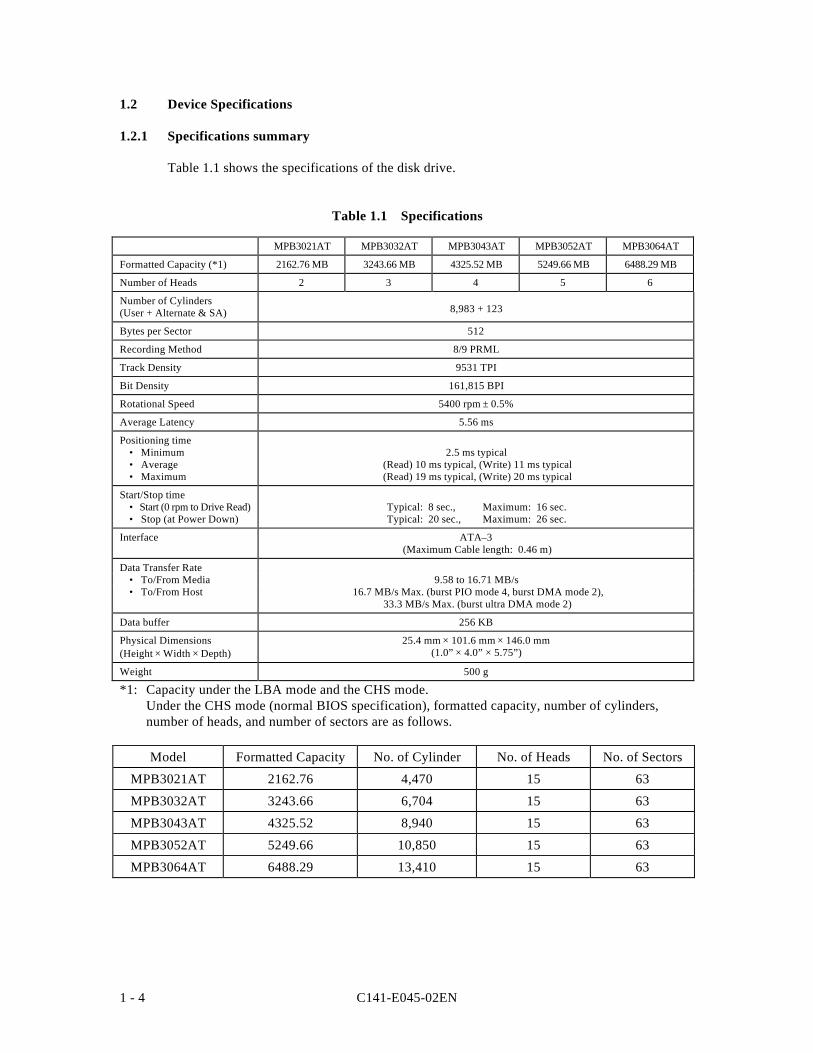
1.2 Device Specifications
1.2.1 Specifications summary
Table 1.1 shows the specifications of the disk drive.
Table 1.1 Specifications
MPB3021AT MPB3032AT MPB3043AT MPB3052AT MPB3064AT
Formatted Capacity (*1) 2162.76 MB 3243.66 MB 4325.52 MB 5249.66 MB 6488.29 MB
Number of Heads 2 3 4 5 6
Number of Cylinders(User + Alternate & SA) 8,983 + 123
Bytes per Sector 512
Recording Method 8/9 PRML
Track Density 9531 TPI
Bit Density 161,815 BPI
Rotational Speed 5400 rpm ± 0.5%
Average Latency 5.56 ms
Positioning time• Minimum• Average• Maximum
2.5 ms typical(Read) 10 ms typical, (Write) 11 ms typical(Read) 19 ms typical, (Write) 20 ms typical
Start/Stop time• Start (0 rpm to Drive Read)• Stop (at Power Down)
Typical: 8 sec., Maximum: 16 sec.Typical: 20 sec., Maximum: 26 sec.
Interface ATA–3(Maximum Cable length: 0.46 m)
Data Transfer Rate• To/From Media 9.58 to 16.71 MB/s• To/From Host 16.7 MB/s Max. (burst PIO mode 4, burst DMA mode 2),
33.3 MB/s Max. (burst ultra DMA mode 2)
Data buffer 256 KB
Physical Dimensions(Height × Width × Depth)
25.4 mm × 101.6 mm × 146.0 mm(1.0” × 4.0” × 5.75”)
Weight 500 g
*1: Capacity under the LBA mode and the CHS mode.Under the CHS mode (normal BIOS specification), formatted capacity, number of cylinders,number of heads, and number of sectors are as follows.
Model Formatted Capacity No. of Cylinder No. of Heads No. of Sectors
MPB3021AT 2162.76 4,470 15 63
MPB3032AT 3243.66 6,704 15 63
MPB3043AT 4325.52 8,940 15 63
MPB3052AT 5249.66 10,850 15 63
MPB3064AT 6488.29 13,410 15 63
C141-E045-02EN 1 - 5
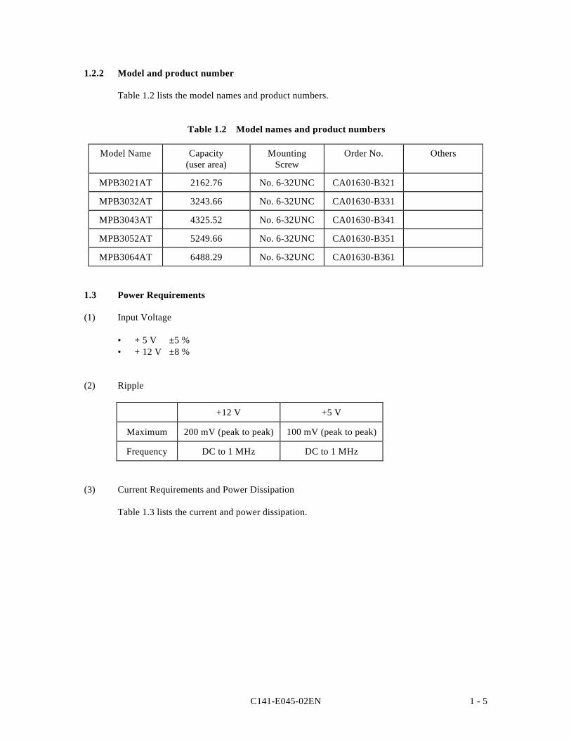
1.2.2 Model and product number
Table 1.2 lists the model names and product numbers.
Table 1.2 Model names and product numbers
Model Name Capacity(user area)
MountingScrew
Order No. Others
MPB3021AT 2162.76 No. 6-32UNC CA01630-B321
MPB3032AT 3243.66 No. 6-32UNC CA01630-B331
MPB3043AT 4325.52 No. 6-32UNC CA01630-B341
MPB3052AT 5249.66 No. 6-32UNC CA01630-B351
MPB3064AT 6488.29 No. 6-32UNC CA01630-B361
1.3 Power Requirements
(1) Input Voltage
• + 5 V ±5 %• + 12 V ±8 %
(2) Ripple
+12 V +5 V
Maximum 200 mV (peak to peak) 100 mV (peak to peak)
Frequency DC to 1 MHz DC to 1 MHz
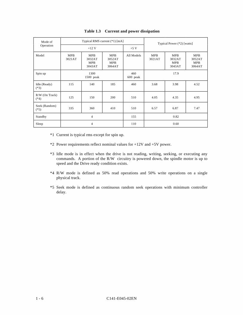
(3) Current Requirements and Power Dissipation
Table 1.3 lists the current and power dissipation.
C141-E045-02EN1 - 6
Table 1.3 Current and power dissipation
Typical RMS current (*1) [mA]
+12 V +5 V
Model MPB3021AT
MPB3032AT
MPB3043AT
MPB3052AT
MPB3064AT
All Models MPB3021AT
MPB3032AT
MPB3043AT
MPB3052AT
MPB3064AT
Spin up 13001500 peak
460600 peak
17.9
Idle (Ready)(*3)
115 140 185 460 3.68 3.98 4.52
R/W (On Track)(*4) 125 150 200 510 4.05 4.35 4.95
Seek (Random)(*5) 335 360 410 510 6.57 6.87 7.47
Standby 4 155 0.82
Sleep 4 110 0.60
*1 Current is typical rms except for spin up.
*2 Power requirements reflect nominal values for +12V and +5V power.
*3 Idle mode is in effect when the drive is not reading, writing, seeking, or executing anycommands. A portion of the R/W circuitry is powered down, the spindle motor is up tospeed and the Drive ready condition exists.
*4 R/W mode is defined as 50% read operations and 50% write operations on a singlephysical track.
*5 Seek mode is defined as continuous random seek operations with minimum controllerdelay.
Typical Power (*2) [watts]Mode ofOperation
C141-E045-02EN 1 - 7
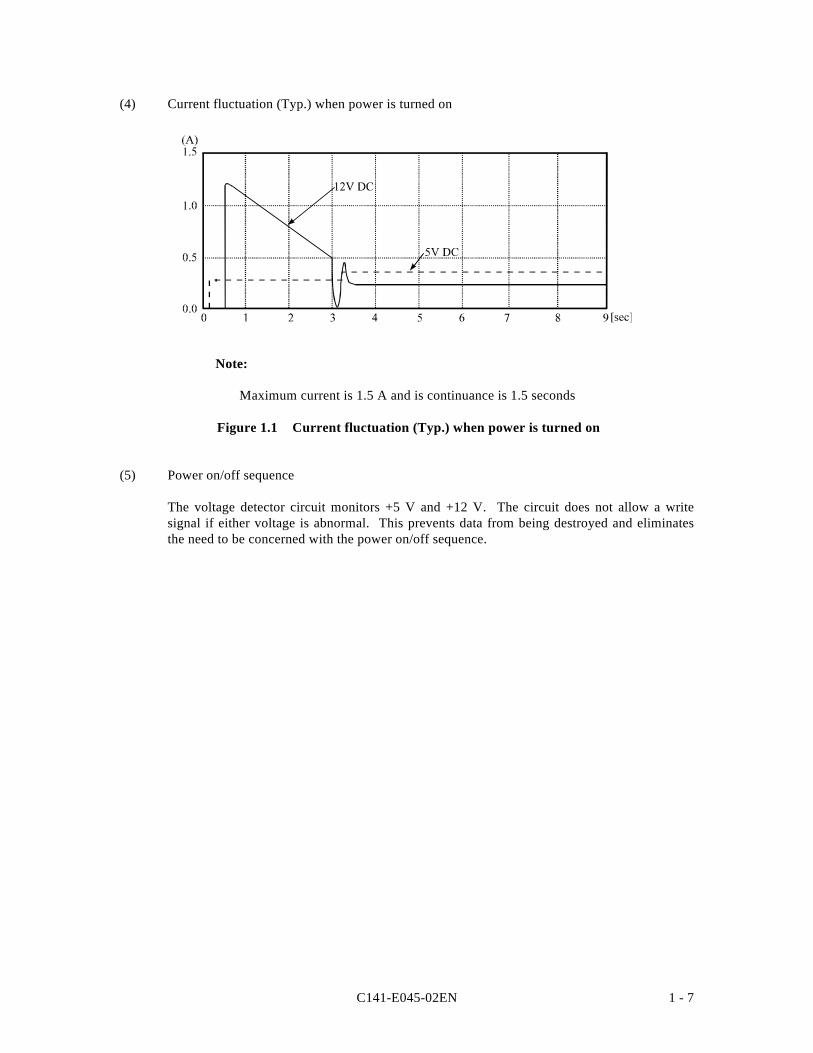
(4) Current fluctuation (Typ.) when power is turned on
Note:
Maximum current is 1.5 A and is continuance is 1.5 seconds
Figure 1.1 Current fluctuation (Typ.) when power is turned on
(5) Power on/off sequence
The voltage detector circuit monitors +5 V and +12 V. The circuit does not allow a writesignal if either voltage is abnormal. This prevents data from being destroyed and eliminatesthe need to be concerned with the power on/off sequence.
C141-E045-02EN1 - 8
1.4 Environmental Specifications
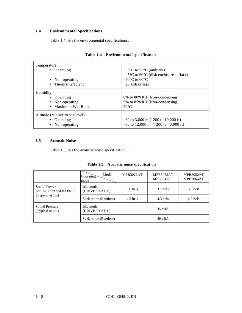
Table 1.4 lists the environmental specifications.
Table 1.4 Environmental specifications
Temperature• Operating
• Non-operating• Thermal Gradient
5°C to 55°C (ambient) 5°C to 60°C (disk enclosure surface)–40°C to 60°C 20°C/h or less
Humidity• Operating• Non-operating• Maximum Wet Bulb
8% to 80%RH (Non-condensing)5% to 85%RH (Non-condensing)29°C
Altitude (relative to sea level)• Operating• Non-operating
–60 to 3,000 m (–200 to 10,000 ft)–60 to 12,000 m (–200 to 40,000 ft)
1.5 Acoustic Noise
Table 1.5 lists the acoustic noise specification.
Table 1.5 Acoustic noise specification
Model MPB3021AT MPB3032ATMPB3043AT
MPB3052ATMPB3064AT
Idle mode(DRIVE READY) 3.6 bels 3.7 bels 3.8 bels
Seek mode (Random) 4.2 bels 4.3 bels 4.3 bels
Sound Pressure(Typical at 1m)
Idle mode(DRIVE READY) 35 dBA
Seek mode (Random) 40 dBA
Operatingmode
Sound Powerper ISO7779 and ISO9296(Typical at 1m)
C141-E045-02EN 1 - 9
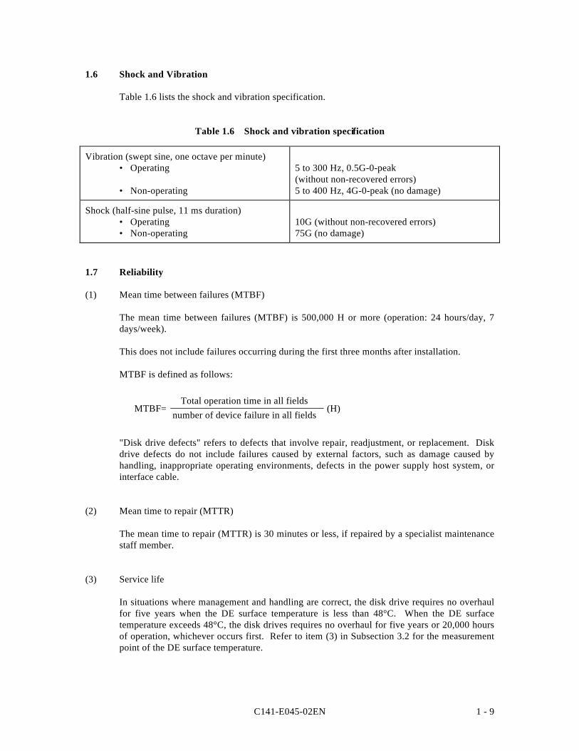
1.6 Shock and Vibration
Table 1.6 lists the shock and vibration specification.
Table 1.6 Shock and vibration specification
Vibration (swept sine, one octave per minute)• Operating
• Non-operating
5 to 300 Hz, 0.5G-0-peak(without non-recovered errors)5 to 400 Hz, 4G-0-peak (no damage)
Shock (half-sine pulse, 11 ms duration)• Operating• Non-operating
10G (without non-recovered errors)75G (no damage)
1.7 Reliability
(1) Mean time between failures (MTBF)
The mean time between failures (MTBF) is 500,000 H or more (operation: 24 hours/day, 7days/week).
This does not include failures occurring during the first three months after installation.
MTBF is defined as follows:
MTBF= (H)
"Disk drive defects" refers to defects that involve repair, readjustment, or replacement. Diskdrive defects do not include failures caused by external factors, such as damage caused byhandling, inappropriate operating environments, defects in the power supply host system, orinterface cable.
(2) Mean time to repair (MTTR)
The mean time to repair (MTTR) is 30 minutes or less, if repaired by a specialist maintenancestaff member.
(3) Service life
In situations where management and handling are correct, the disk drive requires no overhaulfor five years when the DE surface temperature is less than 48°C. When the DE surfacetemperature exceeds 48°C, the disk drives requires no overhaul for five years or 20,000 hoursof operation, whichever occurs first. Refer to item (3) in Subsection 3.2 for the measurementpoint of the DE surface temperature.
Total operation time in all fieldsnumber of device failure in all fields
C141-E045-02EN1 - 10
(4) Data assurance in the event of power failure
Except for the data block being written to, the data on the disk media is assured in the event ofany power supply abnormalities. This does not include power supply abnormalities duringdisk media initialization (formatting) or processing of defects (alternative block assignment).
1.8 Error Rate
Known defects, for which alternative blocks can be assigned, are not included in the error ratecount below. It is assumed that the data blocks to be accessed are evenly distributed on thedisk media.
(1) Unrecoverable read error
Read errors that cannot be recovered by maximum 126 times read retries without user's retryand ECC corrections shall occur no more than 10 times when reading data of 1015 bits. Readretries are executed according to the disk drive's error recovery procedure, and include readretries accompanying head offset operations.
(2) Positioning error
Positioning (seek) errors that can be recovered by one retry shall occur no more than 10 timesin 107 seek operations.
1.9 Media Defects
Defective sectors are replaced with alternates when the disk is formatted prior to shipmentfrom the factory (low level format). Thus, the host sees a defect-free device.
Alternate sectors are automatically accessed by the disk drive. The user need not be concernedwith access to alternate sectors.
Chapter 6 describes the low level format at shipping.
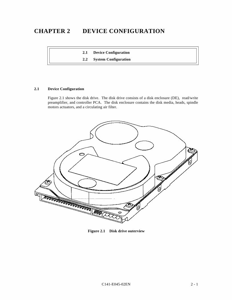
C141-E045-02EN 2 - 1
CHAPTER 2 DEVICE CONFIGURATION
2.1 Device Configuration
2.2 System Configuration
2.1 Device Configuration
Figure 2.1 shows the disk drive. The disk drive consists of a disk enclosure (DE), read/writepreamplifier, and controller PCA. The disk enclosure contains the disk media, heads, spindlemotors actuators, and a circulating air filter.
Figure 2.1 Disk drive outerview
C141-E045-02EN2 - 2
(1) Disk
The outer diameter of the disk is 95 mm. The inner diameter is 25 mm. The number of disksused varies with the model, as described below. The disks are rated at over 40,000 start/stopoperations.
MPB3021AT: 1 diskMPB3032AT: 2 disksMPB3043AT: 2 disks
MPB3052AT: 3 disksMPB3064AT: 3 disks
(2) Head
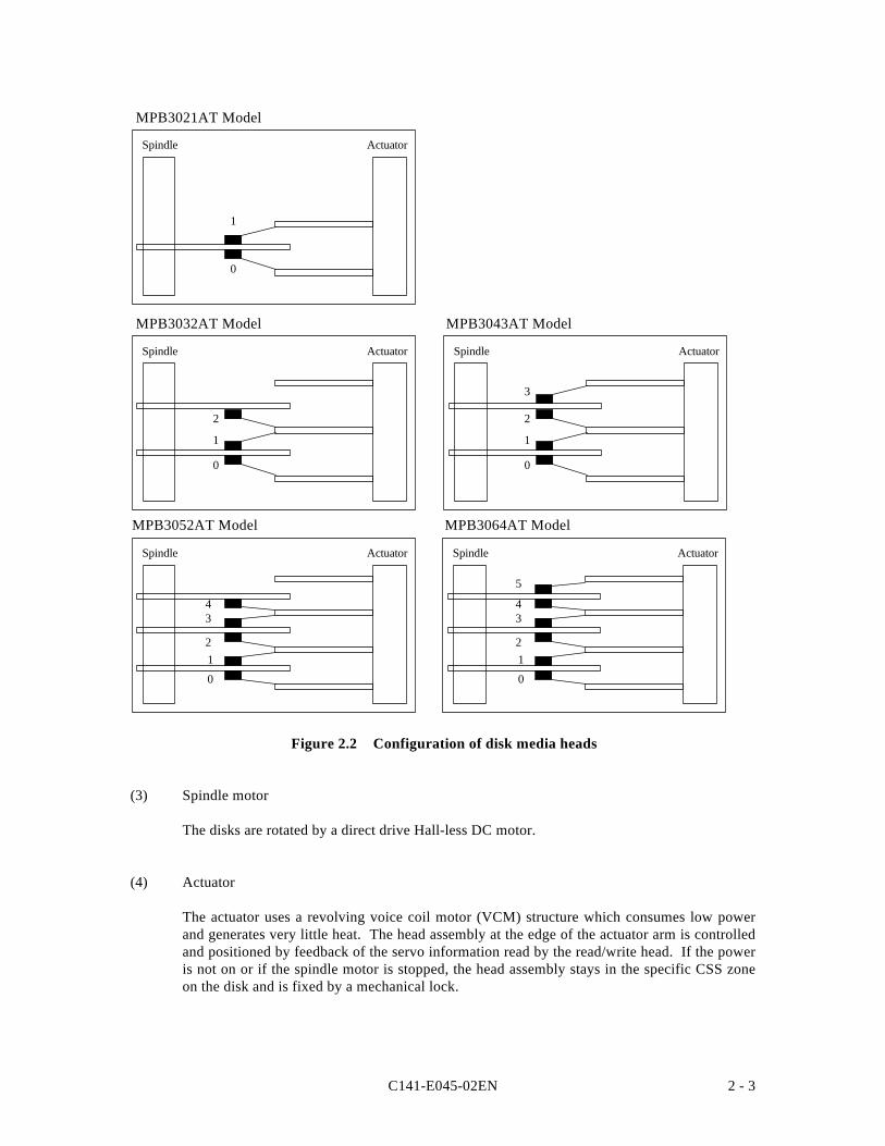
The heads are of the contact start/stop (CSS) type. The head touches the disk surface while thedisk is not rotating and automatically lifts when the disk starts.
Figure 2.2 illustrates the configuration of the disks and heads of each model. In the disksurface, servo information necessary for controlling positioning and read/write and user dataare written. Numerals 0 to 5 indicate read/write heads.
C141-E045-02EN 2 - 3
Spindle
0
1
Actuator
MPB3021 Model
MPB3032AT Model
Spindle
1
2
0
Actuator
MPB3052AT Model
Spindle
2
34
0
1
Actuator
MPB3043AT Model
Spindle
1
3
2
0
Actuator
MPB3064AT Model
Spindle
2
3
5
4
0
1
Actuator
Figure 2.2 Configuration of disk media heads
(3) Spindle motor
The disks are rotated by a direct drive Hall-less DC motor.
(4) Actuator
The actuator uses a revolving voice coil motor (VCM) structure which consumes low powerand generates very little heat. The head assembly at the edge of the actuator arm is controlledand positioned by feedback of the servo information read by the read/write head. If the poweris not on or if the spindle motor is stopped, the head assembly stays in the specific CSS zoneon the disk and is fixed by a mechanical lock.
MPB3052AT Model MPB3064AT Model
MPB3043AT ModelMPB3032AT Model
MPB3021AT Model
C141-E045-02EN2 - 4
(5) Air circulation system
The disk enclosure (DE) is sealed to prevent dust and dirt from entering. The disk enclosurefeatures a closed loop air circulation system that relies on the blower effect of the rotatingdisk. This system continuously circulates the air through the circulation filter to maintain thecleanliness of the air within the disk enclosure.
(6) Read/write circuit
The read/write circuit uses a LSI chip for the read/write preamplifier. It improves datareliability by preventing errors caused by external noise.
(7) Controller circuit
The controller circuit consists of an LSI chip to improve reliability. The high-speedmicroprocessor unit (MPU) achieves a high-performance AT controller.
2.2 System Configuration
2.2.1 ATA interface
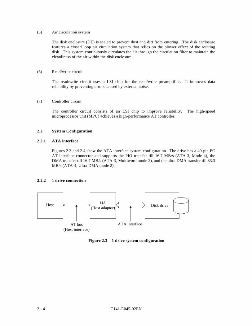
Figures 2.3 and 2.4 show the ATA interface system configuration. The drive has a 40-pin PCAT interface connector and supports the PIO transfer till 16.7 MB/s (ATA-3, Mode 4), theDMA transfer till 16.7 MB/s (ATA-3, Multiword mode 2), and the ultra DMA transfer till 33.3MB/s (ATA-4, Ultra DMA mode 2).
2.2.2 1 drive connection
ATA interfaceAT bus(Host interface)
Disk driveHA(Host adaptor)
Host
Figure 2.3 1 drive system configuration
C141-E045-02EN 2 - 5
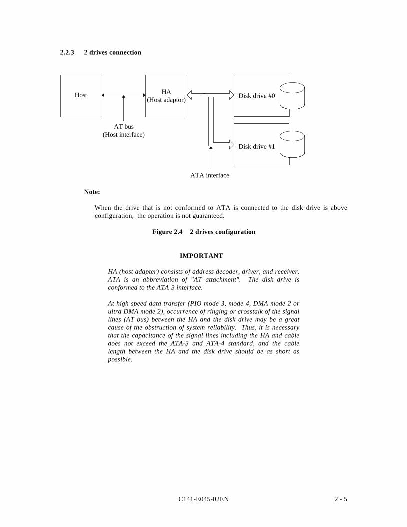
2.2.3 2 drives connection
ATA interface
AT bus(Host interface)
Disk drive #1
Disk drive #0HA(Host adaptor)
Host
Note:
When the drive that is not conformed to ATA is connected to the disk drive is aboveconfiguration, the operation is not guaranteed.
Figure 2.4 2 drives configuration
IMPORTANT
HA (host adapter) consists of address decoder, driver, and receiver.ATA is an abbreviation of "AT attachment". The disk drive isconformed to the ATA-3 interface.
At high speed data transfer (PIO mode 3, mode 4, DMA mode 2 orultra DMA mode 2), occurrence of ringing or crosstalk of the signallines (AT bus) between the HA and the disk drive may be a greatcause of the obstruction of system reliability. Thus, it is necessarythat the capacitance of the signal lines including the HA and cabledoes not exceed the ATA-3 and ATA-4 standard, and the cablelength between the HA and the disk drive should be as short aspossible.

C141-E045-02EN 3 - 1
CHAPTER 3 INSTALLATION CONDITIONS
3.1 Dimensions
3.2 Mounting
3.3 Cable Connections
3.4 Jumper Settings
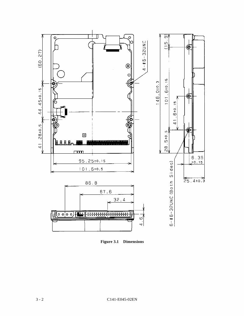
3.1 Dimensions
Figure 3.1 illustrates the dimensions of the disk drive and positions of the mounting screwholes. All dimensions are in mm.
C141-E045-02EN3 - 2
Figure 3.1 Dimensions
C141-E045-02EN 3 - 3
3.2 Mounting
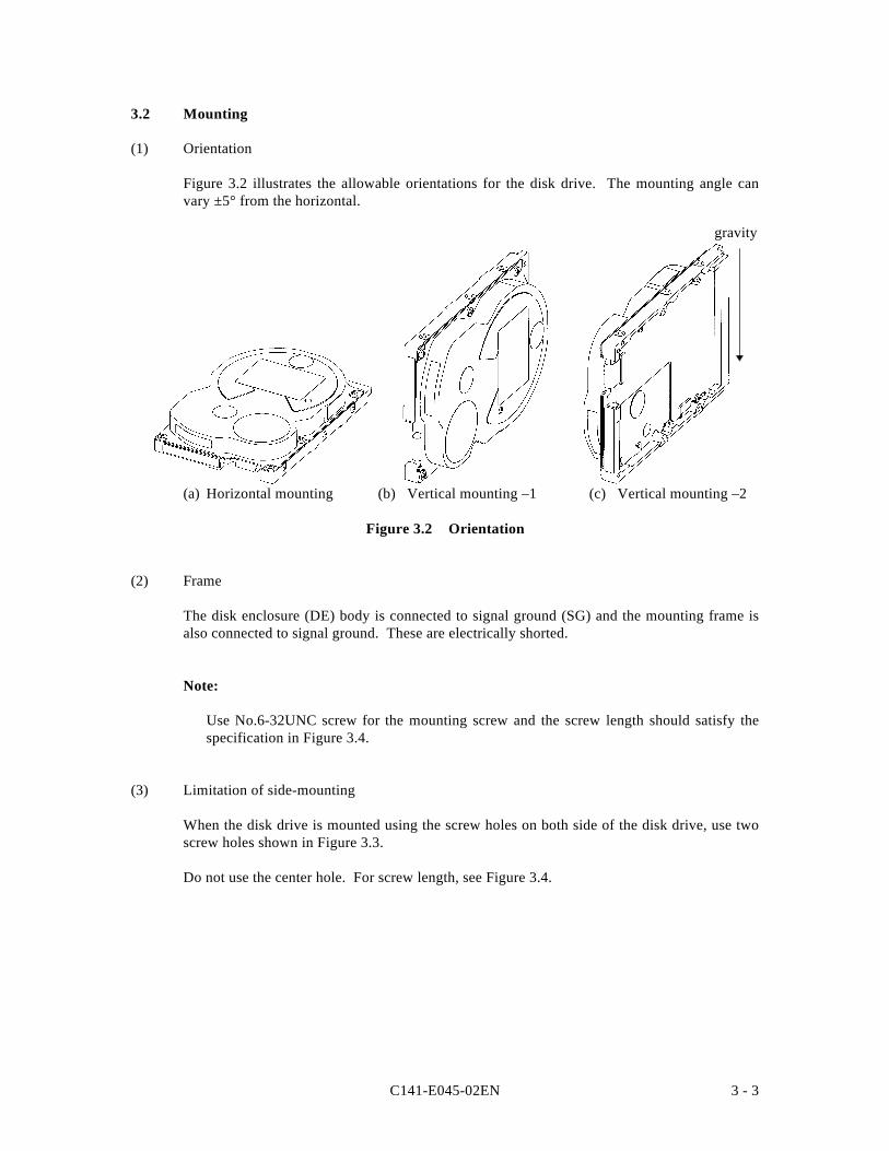
(1) Orientation
Figure 3.2 illustrates the allowable orientations for the disk drive. The mounting angle canvary ±5° from the horizontal.
(a) Horizontal mounting (b) Vertical mounting –1 (c) Vertical mounting –2
Figure 3.2 Orientation
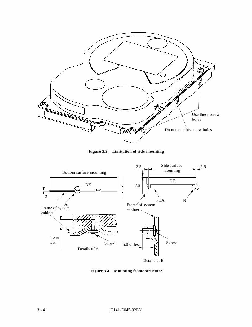
(2) Frame
The disk enclosure (DE) body is connected to signal ground (SG) and the mounting frame isalso connected to signal ground. These are electrically shorted.
Note:
Use No.6-32UNC screw for the mounting screw and the screw length should satisfy thespecification in Figure 3.4.
(3) Limitation of side-mounting
When the disk drive is mounted using the screw holes on both side of the disk drive, use twoscrew holes shown in Figure 3.3.
Do not use the center hole. For screw length, see Figure 3.4.
gravity
C141-E045-02EN3 - 4
Figure 3.3 Limitation of side-mounting
Figure 3.4 Mounting frame structure
5.0 or less
4.5 orless
2B
Frame of systemcabinet
Details of B
Details of A
Frame of systemcabinet
Screw Screw
PCA
DE
2.5
2.5
2.5
A
DE
Side surfacemountingBottom surface mounting
Do not use this screw holes
Use these screwholes
C141-E045-02EN 3 - 5
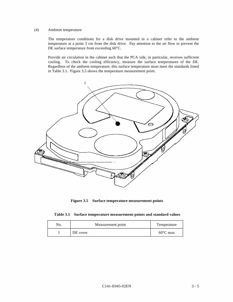
(4) Ambient temperature
The temperature conditions for a disk drive mounted in a cabinet refer to the ambienttemperature at a point 3 cm from the disk drive. Pay attention to the air flow to prevent theDE surface temperature from exceeding 60°C.
Provide air circulation in the cabinet such that the PCA side, in particular, receives sufficientcooling. To check the cooling efficiency, measure the surface temperatures of the DE.Regardless of the ambient temperature, this surface temperature must meet the standards listedin Table 3.1. Figure 3.5 shows the temperature measurement point.
Figure 3.5 Surface temperature measurement points
Table 3.1 Surface temperature measurement points and standard values
No. Measurement point Temperature
1 DE cover 60°C max
1
C141-E045-02EN3 - 6
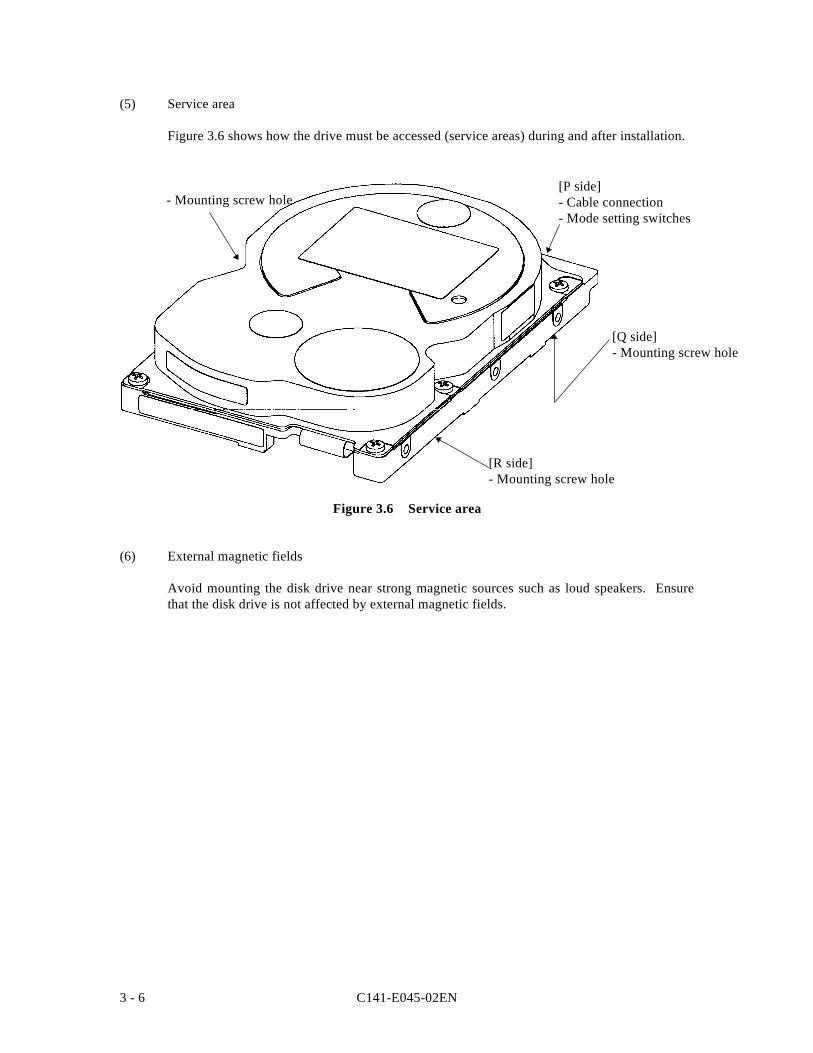
(5) Service area
Figure 3.6 shows how the drive must be accessed (service areas) during and after installation.
Figure 3.6 Service area
(6) External magnetic fields
Avoid mounting the disk drive near strong magnetic sources such as loud speakers. Ensurethat the disk drive is not affected by external magnetic fields.
[P side]- Cable connection- Mode setting switches
[R side]- Mounting screw hole
- Mounting screw hole
[Q side]- Mounting screw hole
C141-E045-02EN 3 - 7
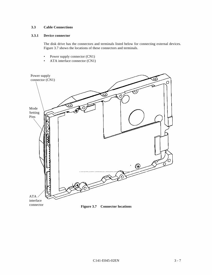
3.3 Cable Connections
3.3.1 Device connector
The disk drive has the connectors and terminals listed below for connecting external devices.Figure 3.7 shows the locations of these connectors and terminals.
• Power supply connector (CN1)• ATA interface connector (CN1)
Figure 3.7 Connector locations
ATAinterfaceconnector
ModeSettingPins
Power supplyconnector (CN1)
C141-E045-02EN3 - 8
3.3.2 Cable connector specifications
Table 3.2 lists the recommended specifications for the cable connectors.
Table 3.2 Cable connector specifications
Name Model Manufacturer
Cable socket(closed-end type) FCN-707B040-AU/B Fujitsu
Cable socket(through-end type) FCN-707B040-AU/O Fujitsu
Signal cable 445-248-40 SPECTERS STRIP
Cable socket housing 1-480424-0 AMP
Contact 60617-4 AMP
Signal cable AWG 18 to 24
Note :
The cable of twisted pairs and neighboring line separated individually is not allowed to usefor the host interface cable. It is because that the location of signal lines in these cables isnot fixed, and so the problem on the crosstalk among signal lines may occur.
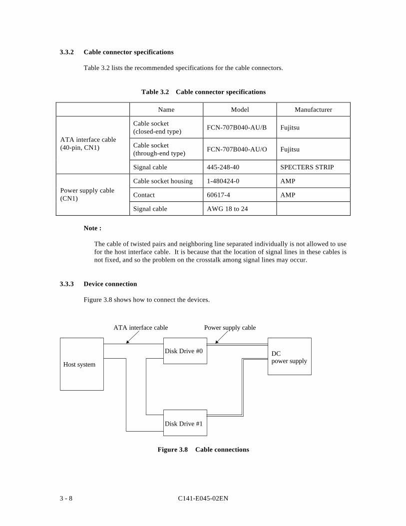
3.3.3 Device connection
Figure 3.8 shows how to connect the devices.
ATA interface cable Power supply cable
DCpower supply
Disk Drive #1
Disk Drive #0
Host system
Figure 3.8 Cable connections
Power supply cable(CN1)
ATA interface cable(40-pin, CN1)
C141-E045-02EN 3 - 9
3.3.4 Power supply connector (CN1)
Figure 3.9 shows the pin assignment of the power supply connector (CN1).
(Viewed from cable side)
4321
+5VDC
+5V RETURN
+12V RETURN
+12VDC
4
3
2
1
Figure 3.9 Power supply connector pins (CN1)
3.4 Jumper Settings
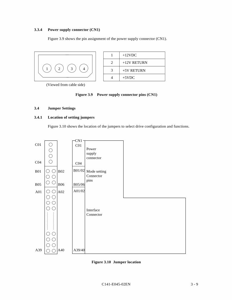
3.4.1 Location of setting jumpers
Figure 3.10 shows the location of the jumpers to select drive configuration and functions.
A39 A40
InterfaceConnector
Mode settingConnectorpins
Powersupplyconnector
C01
C04
B01/02
B06B05 B05/06
A01/02
A39/40
CN1
A01 A02
B02
C04
C01
B01
Figure 3.10 Jumper location
C141-E045-02EN3 - 10
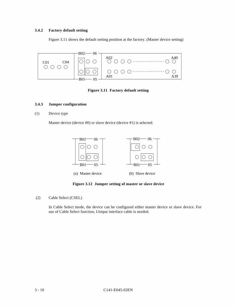
3.4.2 Factory default setting
Figure 3.11 shows the default setting position at the factory. (Master device setting)
C04
A01
A02C01
A39
A40
05
06
B01
B02
Figure 3.11 Factory default setting
3.4.3 Jumper configuration
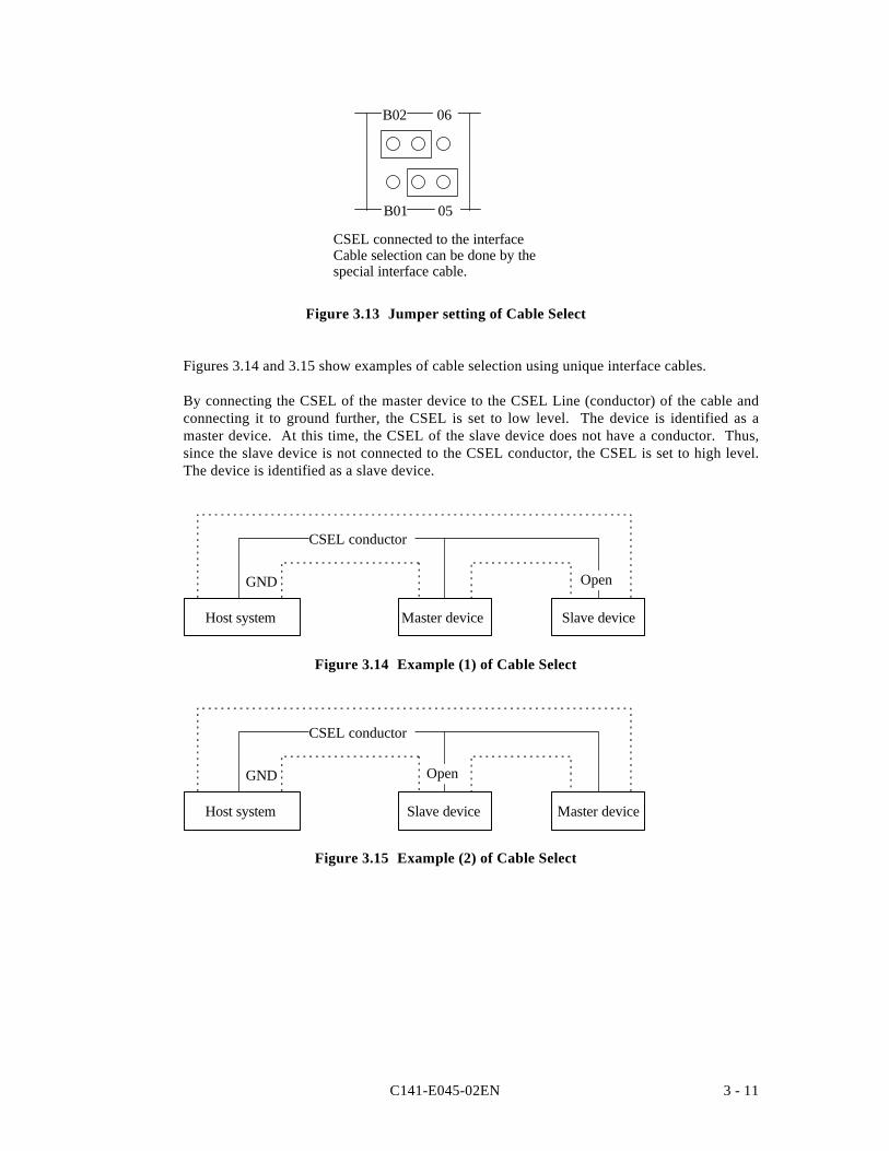
(1) Device type
Master device (device #0) or slave device (device #1) is selected.
06B02
05B01
(a) Master device (b) Slave device
B01 05
06B02
Figure 3.12 Jumper setting of master or slave device
(2) Cable Select (CSEL)
In Cable Select mode, the device can be configured either master device or slave device. Foruse of Cable Select function, Unique interface cable is needed.
C141-E045-02EN 3 - 11
06B02
CSEL connected to the interfaceCable selection can be done by thespecial interface cable.
B01 05
Figure 3.13 Jumper setting of Cable Select
Figures 3.14 and 3.15 show examples of cable selection using unique interface cables.
By connecting the CSEL of the master device to the CSEL Line (conductor) of the cable andconnecting it to ground further, the CSEL is set to low level. The device is identified as amaster device. At this time, the CSEL of the slave device does not have a conductor. Thus,since the slave device is not connected to the CSEL conductor, the CSEL is set to high level.The device is identified as a slave device.
Open
CSEL conductor
GND
Slave deviceMaster deviceHost system
Figure 3.14 Example (1) of Cable Select
Slave device Master device
CSEL conductor
GND
Host system
Open
Figure 3.15 Example (2) of Cable Select
C141-E045-02EN3 - 12
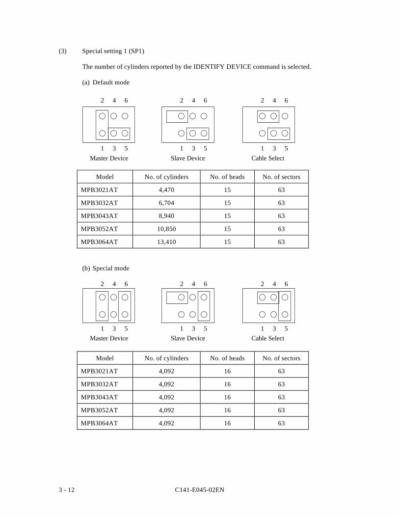
(3) Special setting 1 (SP1)
The number of cylinders reported by the IDENTIFY DEVICE command is selected.
(a) Default mode
2 4 6
1 3 5
2 4 6
Slave DeviceMaster Device1 3 5
2 4 6
1 3 5Cable Select
Model No. of cylinders No. of heads No. of sectors
MPB3021AT 4,470 15 63
MPB3032AT 6,704 15 63
MPB3043AT 8,940 15 63
MPB3052AT 10,850 15 63
MPB3064AT 13,410 15 63
(b) Special mode
2 4 6
1 3 5
2 4 6
Slave DeviceMaster Device1 3 5
2 4 6
1 3 5Cable Select
Model No. of cylinders No. of heads No. of sectors
MPB3021AT 4,092 16 63
MPB3032AT 4,092 16 63
MPB3043AT 4,092 16 63
MPB3052AT 4,092 16 63
MPB3064AT 4,092 16 63
C141-E045-02EN 4 - 1
CHAPTER 4 THEORY OF DEVICE OPERATION
4.1 Outline
4.2 Subassemblies
4.3 Circuit Configuration
4.4 Power-on sequence
4.5 Self-calibration
4.6 Read/Write Circuit
4.7 Servo Control
This chapter explains basic design concepts of the disk drive. Also, this chapter explainssubassemblies of the disk drive, each sequence, servo control, and electrical circuit blocks.
4.1 Outline
This chapter consists of two parts. First part (Section 4.2) explains mechanical assemblies ofthe disk drive. Second part (Sections 4.3 through 4.7) explains a servo information recordedin the disk drive and drive control method.
4.2 Subassemblies
The disk drive consists of a disk enclosure (DE) and printed circuit assembly (PCA).
The DE contains all movable parts in the disk drive, including the disk, spindle, actuator,read/write head, and air filter. For details, see Subsections 4.2.1 to 4.2.5.
The PCA contains the control circuits for the disk drive. The disk drive has one PCA. Fordetails, see Sections 4.3.
4.2.1 Disk
The DE contains the disks with an outer diameter of 95 mm. The MPB3021AT has 1 disk, theMPB3032AT and MPB3043AT have 2 disks. MPB3052AT and MPB3064AT have 3 disks.
The head contacts the disk each time the disk rotation stops; the life of the disk is 40,000contacts or more.
Servo data is recorded on each cylinder (total 60). Servo data written at factory is read out bythe read/write head. For servo data, see Section 4.7.
C141-E045-02EN4 - 2
4.2.2 Head
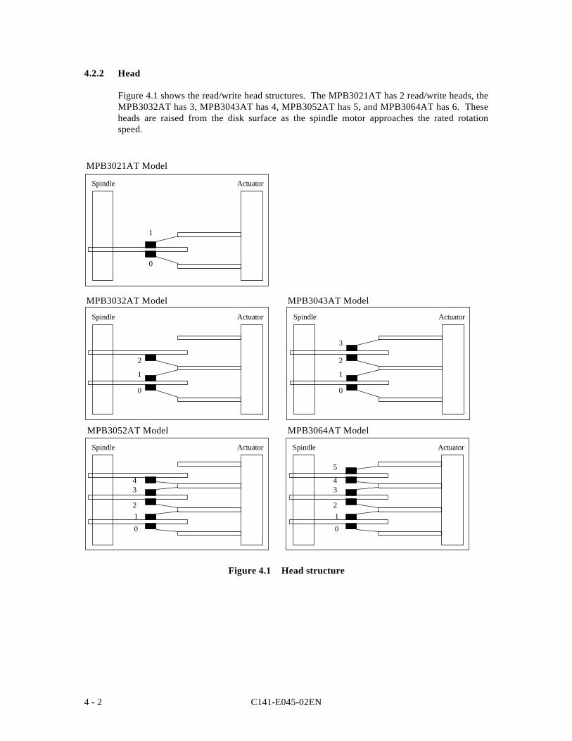
Figure 4.1 shows the read/write head structures. The MPB3021AT has 2 read/write heads, theMPB3032AT has 3, MPB3043AT has 4, MPB3052AT has 5, and MPB3064AT has 6. Theseheads are raised from the disk surface as the spindle motor approaches the rated rotationspeed.
Spindle
0
1
Actuator
MPB3021 Model
MPB3032AT Model
Spindle
1
2
0
Actuator
MPB3052AT Model
Spindle
2
34
0
1
Actuator
MPB3043AT Model
Spindle
1
3
2
0
Actuator
MPB3064AT Model
Spindle
2
3
5
4
0
1
Actuator
Figure 4.1 Head structure
MPB3052AT Model MPB3064AT Model
MPB3043AT ModelMPB3032AT Model
MPB3021AT Model
C141-E045-02EN 4 - 3
4.2.3 Spindle
The spindle consists of a disk stack assembly and spindle motor. The disk stack assembly isactivated by the direct drive sensor-less DC spindle motor, which has a speed of 5,400 rpm±0.5%. The spindle is controlled with detecting a PHASE signal generated by counterelectromotive voltage of the spindle motor at starting. After that, the rotational speed is keptwith detecting a servo information.
4.2.4 Actuator
The actuator consists of a voice coil motor (VCM) and a head carriage. The VCM moves thehead carriage along the inner or outer edge of the disk. The head carriage position iscontrolled by feeding back the difference of the target position that is detected and reproducedfrom the servo information read by the read/write head.
4.2.5 Air filter
There are two types of air filters: a breather filter and a circulation filter.
The breather filter makes an air in and out of the DE to prevent unnecessary pressure aroundthe spindle when the disk starts or stops rotating. When disk drives are transported underconditions where the air pressure changes a lot, filtered air is circulated in the DE.
The circulation filter cleans out dust and dirt from inside the DE. The disk drive cycles aircontinuously through the circulation filter through an enclosed loop air cycle system operatedby a blower on the rotating disk.
C141-E045-02EN4 - 4
4.3 Circuit Configuration
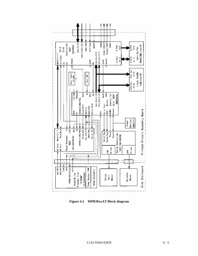
Figure 4.2 shows the disk drive circuit configuration.
(1) Read/write circuit
The read/write circuit consists of two LSIs; read/write preamplifier (PreAMP) and readchannel (RDC).
The PreAMP consists of the write current switch circuit, that flows the write current to thehead coil, and the voltage amplifier circuit, that amplitudes the read output from the head.
The RDC is the read demodulation circuit using the partial response class 4 (PR4), andcontains the Viterbi detector, programmable filter, adaptable transversal filter, times basegenerator, and data separator circuits. The RDC also contains the 8/9 group coded recording(GCR) encoder and decoder and servo demodulation circuit.
(2) Servo circuit
The position and speed of the voice coil motor are controlled by 2 closed-loop servo using theservo information recorded on the data surface. The servo information is an analog signalconverted to digital for processing by a MPU and then reconverted to an analog signal forcontrol of the voice coil motor.
(3) Spindle motor driver circuit
The circuit measures the interval of a PHASE signal generated by counter-electromotivevoltage of a motor, or servo mark at the MPU and controls the motor speed comparing targetspeed.
(4) Controller circuit
Major functions are listed below.
• Data buffer management• ATA interface control and data transfer control• Sector format control• Defect management• ECC control• Error recovery and self-diagnosis
C141-E045-02EN 4 - 5
Figure 4.2 MPB30xxAT Block diagram
C141-E045-02EN4 - 6
4.4 Power-on Sequence
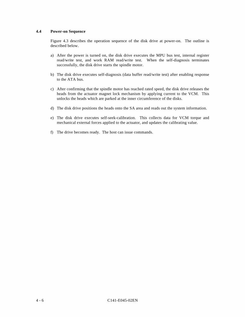
Figure 4.3 describes the operation sequence of the disk drive at power-on. The outline isdescribed below.
a) After the power is turned on, the disk drive executes the MPU bus test, internal registerread/write test, and work RAM read/write test. When the self-diagnosis terminatessuccessfully, the disk drive starts the spindle motor.
b) The disk drive executes self-diagnosis (data buffer read/write test) after enabling responseto the ATA bus.
c) After confirming that the spindle motor has reached rated speed, the disk drive releases theheads from the actuator magnet lock mechanism by applying current to the VCM. Thisunlocks the heads which are parked at the inner circumference of the disks.
d) The disk drive positions the heads onto the SA area and reads out the system information.
e) The disk drive executes self-seek-calibration. This collects data for VCM torque andmechanical external forces applied to the actuator, and updates the calibrating value.
f) The drive becomes ready. The host can issue commands.
C141-E045-02EN 4 - 7
c)
b)
a)
Release heads fromactuator lock
Confirming spindle motorspeed
Self-diagnosis 2• Data buffer write/read test
The spindle motor starts.
Self-diagnosis 1• MPU bus test• Inner register write/read test• Work RAM write/read test
StartPower on
Drive ready state(command waiting state)
Execute self-calibration
Initial on-track and readout of system information
f)
e)
d)
End
Figure 4.3 Power-on operation sequence
C141-E045-02EN4 - 8
4.5 Self-calibration
The disk drive occasionally performs self-calibration in order to sense and calibratemechanical external forces on the actuator, and VCM torque. This enables precise seek andread/write operations.
4.5.1 Self-calibration contents
(1) Sensing and compensating for external forces
The actuator suffers from torque due to the FPC forces and winds accompanying diskrevolution. The torque vary with the disk drive and the cylinder where the head is positioned.To execute stable fast seek operations, external forces are occasionally sensed.
The firmware of the drive measures and stores the force (value of the actuator motor drivecurrent) that balances the torque for stopping head stably. This includes the current offset inthe power amplifier circuit and DAC system.
The forces are compensated by adding the measured value to the specified current value to thepower amplifier. This makes the stable servo control.
To compensate torque varying by the cylinder, the disk is divided into 13 areas from theinnermost to the outermost circumference and the compensating value is measured at themeasuring cylinder on each area at factory calibration. The measured values are stored in theSA cylinder. In the self-calibration, the compensating value is updated using the value in theSA cylinder.
(2) Compensating open loop gain
Torque constant value of the VCM has a dispersion for each drive, and varies depending onthe cylinder that the head is positioned. To realize the high speed seek operation, the valuethat compensates torque constant value change and loop gain change of the whole servosystem due to temperature change is measured and stored.
For sensing, the firmware mixes the disturbance signal to the position signal at the state thatthe head is positioned to any cylinder. The firmware calculates the loop gain from the positionsignal and stores the compensation value against to the target gain as ratio.
For compensating, the direction current value to the power amplifier is multiplied by thecompensation value. By this compensation, loop gain becomes constant value and the stableservo control is realized.
To compensate torque constant value change depending on cylinder, whole cylinders frommost inner to most outer cylinder are divided into 13 partitions at calibration in the factory,and the compensation data is measured for representative cylinder of each partition. Thismeasured value is stored in the SA area. The compensation value at self-calibration iscalculated using the value in the SA area.
C141-E045-02EN 4 - 9
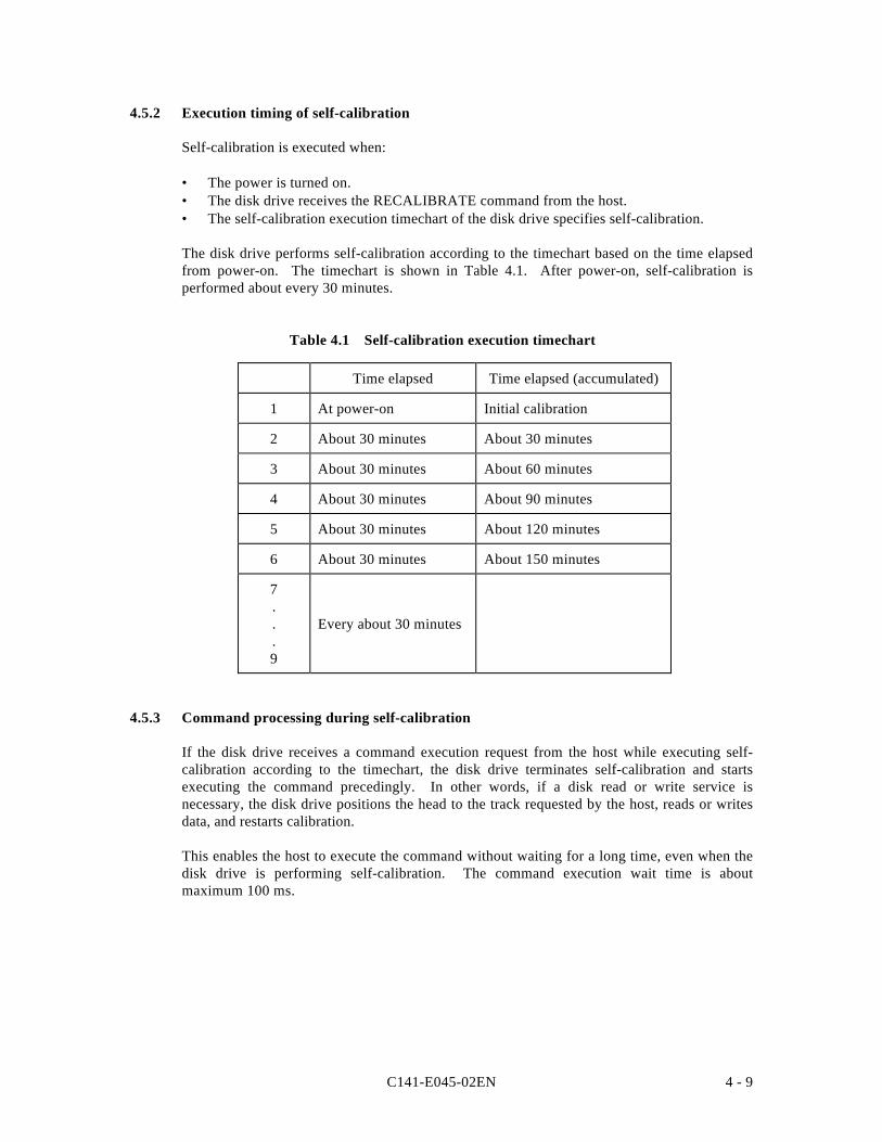
4.5.2 Execution timing of self-calibration
Self-calibration is executed when:
• The power is turned on.• The disk drive receives the RECALIBRATE command from the host.• The self-calibration execution timechart of the disk drive specifies self-calibration.
The disk drive performs self-calibration according to the timechart based on the time elapsedfrom power-on. The timechart is shown in Table 4.1. After power-on, self-calibration isperformed about every 30 minutes.
Table 4.1 Self-calibration execution timechart
Time elapsed Time elapsed (accumulated)
1 At power-on Initial calibration
2 About 30 minutes About 30 minutes
3 About 30 minutes About 60 minutes
4 About 30 minutes About 90 minutes
5 About 30 minutes About 120 minutes
6 About 30 minutes About 150 minutes
7...9
Every about 30 minutes
4.5.3 Command processing during self-calibration
If the disk drive receives a command execution request from the host while executing self-calibration according to the timechart, the disk drive terminates self-calibration and startsexecuting the command precedingly. In other words, if a disk read or write service isnecessary, the disk drive positions the head to the track requested by the host, reads or writesdata, and restarts calibration.
This enables the host to execute the command without waiting for a long time, even when thedisk drive is performing self-calibration. The command execution wait time is aboutmaximum 100 ms.
C141-E045-02EN4 - 10
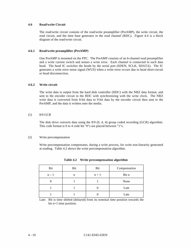
4.6 Read/write Circuit
The read/write circuit consists of the read/write preamplifier (PreAMP), the write circuit, theread circuit, and the time base generator in the read channel (RDC). Figure 4.4 is a blockdiagram of the read/write circuit.
4.6.1 Read/write preamplifier (PreAMP)
One PreAMP is mounted on the FPC. The PreAMP consists of an 6-channel read preamplifierand a write current switch and senses a write error. Each channel is connected to each datahead. The head IC switches the heads by the serial port (SDEN, SCLK, SDATA). The ICgenerates a write error sense signal (WUS) when a write error occurs due to head short-circuitor head disconnection.
4.6.2 Write circuit
The write data is output from the hard disk controller (HDC) with the NRZ data format, andsent to the encoder circuit in the RDC with synchronizing with the write clock. The NRZwrite data is converted from 8-bit data to 9-bit data by the encoder circuit then sent to thePreAMP, and the data is written onto the media.
(1) 8/9 GCR
The disk drive converts data using the 8/9 (0, 4, 4) group coded recording (GCR) algorithm.This code format is 0 to 4 code bit "0"s are placed between "1"s.
(2) Write precompensation
Write precompensation compensates, during a write process, for write non-linearity generatedat reading. Table 4.2 shows the write precompensation algorithm.
Table 4.2 Write precompensation algorithm
Bit Bit Bit Compensation
n – 1 n n + 1 Bit n
0 1 1 None
1 1 0 Late
1 1 0 Late
Late: Bit is time shifted (delayed) from its nominal time position towards thebit n+1 time position.
C141-E045-02EN 4 - 11
Figure 4.4 Read/write circuit block diagram
C141-E045-02EN4 - 12
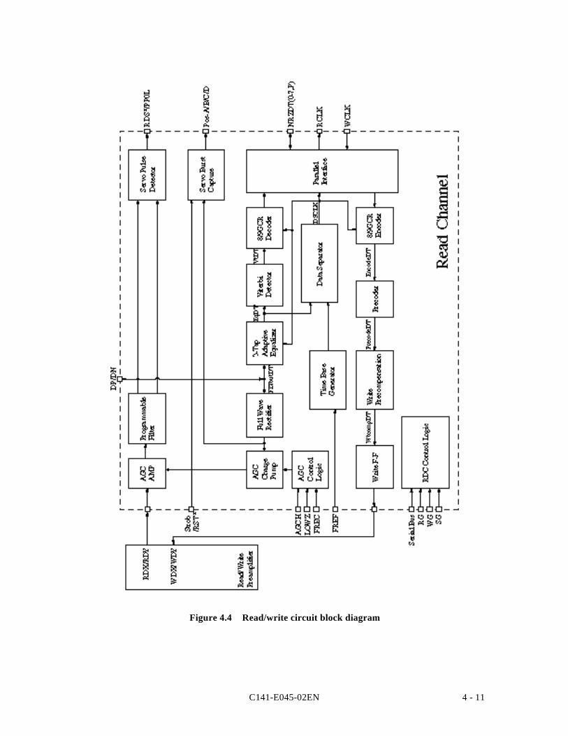
4.6.3 Read circuit
The head read signal from the PreAMP is regulated by the automatic gain control (AGC)circuit. Then the output is converted into the sampled read data pulse by the programmablefilter circuit and the adaptive equalizer circuit. This clock signal is converted into the NRZdata by the 8/9 GCR decoder circuit based on the read data maximum-likelihood-detected bythe Viterbi detection circuit, then is sent to the HDC.
(1) AGC circuit
The AGC circuit automatically regulates the output amplitude to a constant value even whenthe input amplitude level fluctuates. The AGC amplifier output is maintained at a constantlevel even when the head output fluctuates due to the head characteristics or outer/inner headpositions.
(2) Programmable filter
The programmable filter circuit has a low-pass filter function that eliminates unnecessary highfrequency noise component and a high frequency boost-up function that equalizes thewaveform of the read signal.
Cut-off frequency of the low-pass filter and boost-up gain are controlled from each DACcircuit in read channel by an instruction of the serial data signal from MPU (M1). The MPUoptimizes the cut-off frequency and boost-up gain according to the transfer frequency of eachzone.
Figure 4.5 shows the frequency characteristic sample of the programmable filter.
Figure 4.5 Frequency characteristic of programmable filter
(3) Adaptive equalizer circuit
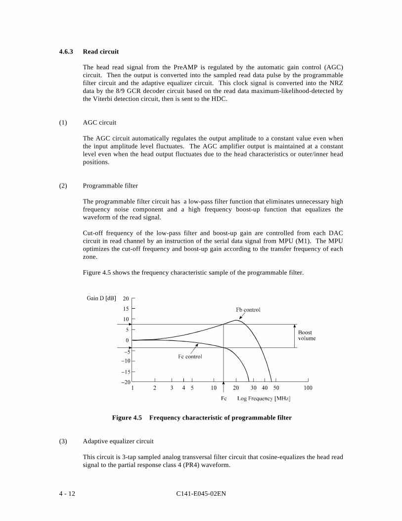
This circuit is 3-tap sampled analog transversal filter circuit that cosine-equalizes the head readsignal to the partial response class 4 (PR4) waveform.
C141-E045-02EN 4 - 13
Figure 4.6 PR4 signal transfer
C141-E045-02EN4 - 14
(4) Viterbi detection circuit
The sample hold waveform output from the adaptive equalizer circuit is sent to the Viterbidetection circuit. The Viterbi detection circuit demodulates data according to the survivorpath sequence.
(5) Data separator circuit
The data separator circuit generates clocks in synchronization with the output of the adaptiveequalizer circuit. To write data, the VFO circuit generates clocks in synchronization with theclock signals from a synthesizer.
(6) 8/9 GCR decoder
This circuit converts the 9-bit read data into the 8-bit NRZ data.
4.6.4 Time base generator circuit
The drive uses constant density recording to increase total capacity. This is different from theconventional method of recording data with a fixed data transfer rate at all data area. In theconstant density recording method, data area is divided into zones by radius and the datatransfer rate is set so that the recording density of the inner cylinder of each zone is nearlyconstant. The drive divides data area into 14 zones to set the data transfer rate. Table 4.3describes the data transfer rate and recording density (BPI) of each zone.
C141-E045-02EN 4 - 15
Table 4.3 Write clock frequency and transfer rate of each zone
Zone 0 1 2 3 4 5 6 7
Cylinder 0to
660
661to
1197
1198to
1938
1939to
2672
2673to
3332
3333to
3958
3959to
4747
4748to
5216
Transfer rate[MB/s] 16.71 16.35 15.82 15.18 14.68 14.15 13.44 13.06
Zone 8 9 10 11 12 13
Cylinder 5217to
5886
5887to
6505
6506to
7073
7074to
8286
8287to
8718
8719to
8982
Transfer rate[MB/s] 12.44 11.85 11.33 10.04 9.74 9.58
The MPU transfers the data transfer rate setup data (SDATA/SCLK) to the RDC that includesthe time base generator circuit to change the data transfer rate.
4.7 Servo Control
The actuator motor and the spindle motor are submitted to servo control. The actuator motoris controlled for moving and positioning the head to the track containing the desired data. Toturn the disk at a constant velocity, the actuator motor is controlled according to the servo datathat is written on the data side beforehand.
C141-E045-02EN4 - 16
4.7.1 Servo control circuit
Figure 4.7 is the block diagram of the servo control circuit. The following describes thefunctions of the blocks:
(5)
(1)
(2) (3) (4)
P.Amp.
CSR: Current Sense ResistorVCM: Voice Coil Motor
Spindlemotorcontrol
DSPunit
Servoburstcapture
SVCMPU
CSR
Driver
DACADC
Position Sense
Head
VCM current
VCM
Spindlemotor
(7)(6)
Figure 4.7 Block diagram of servo control circuit
(1) Microprocessor unit (MPU)
The MPU includes DSP unit, etc., and the MPU starts the spindle motor, moves the heads tothe reference cylinders, seeks the specified cylinder, and executes calibration according to theinternal operations of the MPU.
The major internal operations are listed below.
a. Spindle motor start
Starts the spindle motor and accelerates it to normal speed when power is applied.
b. Move head to reference cylinder
Drives the VCM to position the head at the any cylinder in the data area. The logicalinitial cylinder is at the outermost circumference (cylinder 0).
C141-E045-02EN 4 - 17
c. Seek to specified cylinder
Drives the VCM to position the head to the specified cylinder.
d. Calibration
Senses and stores the thermal offset between heads and the mechanical forces on theactuator, and stores the calibration value.
Figure 4.8 Physical sector servo configuration on disk surface
C141-E045-02EN4 - 18
(2) Servo burst capture circuit
The four servo signals can be synchronously detected by the STROB signal, full-waverectified integrated.
(3) A/D converter (ADC)
The A/D converter (ADC) receives the servo signals are integrated, converts them to digital,and transfers the digital signal to the DSP unit.
(4) D/A converter (DAC)
The D/A converter (DAC) converts the VCM drive current value (digital value) calculated bythe DSP unit into analog values and transfers them to the power amplifier.
(5) Power amplifier
The power amplifier feeds currents, corresponding to the DAC output signal voltage to theVCM.
(6) Spindle motor control circuit
The spindle motor control circuit controls the sensor-less spindle motor. This circuit detectsnumber of revolution of the motor by the interrupt generated periodically, compares with thetarget revolution speed, then flows the current into the motor coil according to thedifferentiation (aberration).
(7) Driver circuit
The driver circuit is a power amplitude circuit that receives signals from the spindle motorcontrol circuit and feeds currents to the spindle motor.
(8) VCM current sense resistor (CSR)
This resistor controls current at the power amplifier by converting the VCM current intovoltage and feeding back.
C141-E045-02EN 4 - 19
4.7.2 Data-surface servo format
Figure 4.8 describes the physical layout of the servo frame. The three areas indicated by (1) to(3) in Figure 4.8 are described below.
(1) Inner guard band
The head is in contact with the disk in this space when the spindle starts turning or stops, andthe rotational speed of the spindle can be controlled on this cylinder area for head moving.
(2) Data area
This area is used as the user data area SA area.
(3) Outer guard band
This area is located at outer position of the user data area, and the rotational speed of thespindle can be controlled on this cylinder area for head moving.
4.7.3 Servo frame format
As the servo information, the drive uses the two-phase servo generated from the gray code andservo A to D. This servo information is used for positioning operation of radius direction andposition detection of circumstance direction.
The servo frame consists of 5 blocks; write/read recovery, servo mark, gray code, servo A toD and PAD. Figure 4.9 shows the servo frame format.
PADServoD
ServoC
ServoB
ServoA
0.54 µs1.32 µs1.32 µs1.32 µs1.26 µs3.06 µs0.54 µs2.34 µs
Gray codeServomark
Write/readrecovery
Figure 4.9 Servo frame format
C141-E045-02EN4 - 20
(1) Write/read recovery
This area is used to absorb the write/read transient and to stabilize the AGC.
(2) Servo mark
This area generates a timing for demodulating the gray code and position-demodulating theservo A to D by detecting the servo mark.
(3) Gray code (including index bit)
This area is used as cylinder address. The data in this area is converted into the binary data bythe gray code demodulation circuit.
(4) Servo A, servo B, servo C, servo D
This area is used as position signals between tracks, and the IDD control at on-track so thatservo A level equals to servo B level.
(5) PAD
This area is used as a gap between servo and data.
4.7.4 Actuator motor control
The voice coil motor (VCM) is controlled by feeding back the servo data recorded on the datasurface. The MPU fetches the position sense data on the servo frame at a constant interval ofsampling time, executes calculation, and updates the VCM drive current.
The servo control of the actuator includes the operation to move the head to the referencecylinder, the seek operation to move the head to the target cylinder to read or write data, andthe track-following operation to position the head onto the target track.
(1) Operation to move the head to the reference cylinder
The MPU moves the head to the reference cylinder when the power is turned. The referencecylinder is in the data area.
When power is applied the heads are moved from the inner circumference shunt zone to thenormal servo data zone in the following sequence:
a) Micro current is fed to the VCM to press the head against the inner circumference.
b) A current is fed to the VCM to move the head toward the outer circumference.
c) When the servo mark is detected the head is moved slowly toward the outer circumferenceat a constant speed.
C141-E045-02EN 4 - 21
d) If the head is stopped at the reference cylinder from there. Track following control starts.
(2) Seek operation
Upon a data read/write request from the host, the MPU confirms the necessity of access to thedisk. If a read or instruction is issued, the MPU seeks the desired track.
The MPU feeds the VCM current via the D/A converter and power amplifier to move thehead. The MPU calculates the difference (speed error) between the specified target positionand the current position for each sampling timing during head moving. The MPU then feedsthe VCM drive current by setting the calculated result into the D/A converter. The calculationis digitally executed by the firmware. When the head arrives at the target cylinder, the track isfollowed.
(3) Track following operation
Except during head movement to the reference cylinder and seek operation under the spindlerotates in steady speed, the MPU does track following control. To position the head at thecenter of a track, the DSP drives the VCM by feeding micro current. For each sampling time,the VCM drive current is determined by filtering the position difference between the targetposition and the position clarified by the detected position sense data. The filtering includesservo compensation. These are digitally controlled by the firmware.
4.7.5 Spindle motor control
Hall-less three-phase twelve-pole motor is used for the spindle motor, and the 3-phasefull/half-wave analog current control circuit is used as the spindle motor driver (called SVChereafter). The firmware operates on the MPU manufactured by Fujitsu. The spindle motor iscontrolled by sending several signals from the MPU to the SVC. There are three modes forthe spindle control; start mode, acceleration mode, and stable rotation mode.
(1) Start mode
When power is supplied, the spindle motor is started in the following sequence:
a) After the power is turned on, the MPU sends a signal to the SVC to charge the changepump capacitor of the SVC. The charged amount defines the current that flows in thespindle motor.
b) When the charge pump capacitor is charged enough, the MPU sets the SVC to the motorstart mode. Then, a current (approx. 1.3 A) flows into the spindle motor.
c) The SVC generates a phase switching signal by itself, and changes the phase of the currentflowed in the motor in the order of (V-phase to U-phase), (W-phase to U-phase), (W-phaseto V-phase), (U-phase to V-phase), (U-phase to W-phase), and (V-phase to W-phase) (afterthat, repeating this order).
d) During phase switching, the spindle motor starts rotating in low speed, and generates acounter electromotive force. The SVC detects this counter electromotive force and reportsto the MPU using a PHASE signal for speed detection.
C141-E045-02EN4 - 22
e) The MPU is waiting for a PHASE signal. When no phase signal is sent for a specificperiod, the MPU resets the SVC and starts from the beginning. When a PHASE signal issent, the SVC enters the acceleration mode.
(2) Acceleration mode
In this mode, the MPU stops to send the phase switching signal to the SVC. The SVC starts aphase switching by itself based on the counter electromotive force. Then, rotation of thespindle motor accelerates. The MPU calculates a rotational speed of the spindle motor basedon the PHASE signal from the SVC, and accelerates till the rotational speed reaches 5,400rpm. When the rotational speed reaches 5,400 rpm, the SVC enters the stable rotation mode.
(3) Stable rotation mode
The MPU calculates a time for one revolution of the spindle motor based on the PHASE signalfrom the SVC. The MPU takes a difference between the current time and a time for onerevolution at 5,400 rpm that the MPU already recognized. Then, the MPU keeps the rotationalspeed to 5,400 rpm by charging or discharging the charge pump for the different time. Forexample, when the actual rotational speed is 5,600 rpm, the time for one revolution is 10.714ms. And, the time for one revolution at 5,400 rpm is 11.111 ms. Therefore, the MPUdischarges the charge pump for 0.397 ms × k (k: constant value). This makes the flowedcurrent into the motor lower and the rotational speed down. When the actual rotational speedis later than 5,400 rpm, the MPU charges the pump the other way. This control(charging/discharging) is performed every 1/6 revolution.
C141-E045-02EN 5 - 1
CHAPTER 5 INTERFACE
5.1 Physical Interface
5.2 Logical Interface
5.3 Host Commands
5.4 Command Protocol
5.5 Ultra DMA feature Set
5.6 Timing
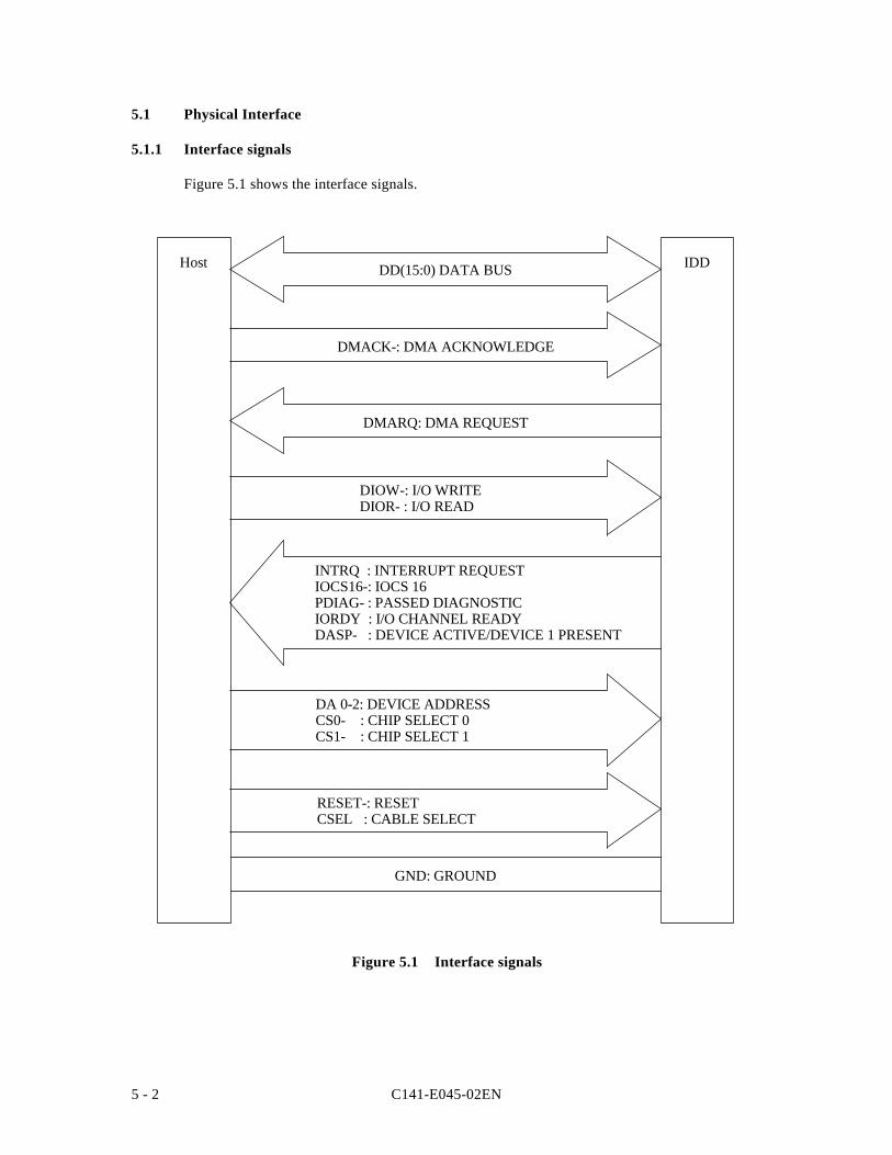
C141-E045-02EN5 - 2
5.1 Physical Interface
5.1.1 Interface signals
Figure 5.1 shows the interface signals.
INTRQ : INTERRUPT REQUESTIOCS16-: IOCS 16PDIAG- : PASSED DIAGNOSTICIORDY : I/O CHANNEL READYDASP- : DEVICE ACTIVE/DEVICE 1 PRESENT
DIOW-: I/O WRITEDIOR- : I/O READ
DMARQ: DMA REQUEST
DMACK-: DMA ACKNOWLEDGE
IDDHost DD(15:0) DATA BUS
DA 0-2: DEVICE ADDRESSCS0- : CHIP SELECT 0CS1- : CHIP SELECT 1
RESET-: RESETCSEL : CABLE SELECT
GND: GROUND
Figure 5.1 Interface signals
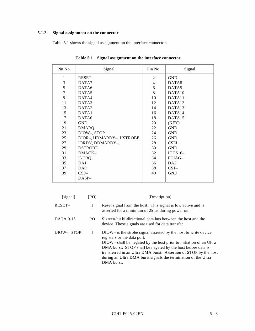
C141-E045-02EN 5 - 3
5.1.2 Signal assignment on the connector
Table 5.1 shows the signal assignment on the interface connector.
Table 5.1 Signal assignment on the interface connector
Pin No. Signal Pin No. Signal
13579
111315171921232527293133353739
RESET–DATA7DATA6DATA5DATA4DATA3DATA2DATA1DATA0GNDDMARQDIOW–, STOPDIOR–, HDMARDY–, HSTROBEIORDY, DDMARDY–,DSTROBEDMACK–INTRQDA1DA0CS0–DASP–
2468
10121416182022242628303234363840
GNDDATA8DATA9DATA10DATA11DATA12DATA13DATA14DATA15(KEY)GNDGNDGNDCSELGNDIOCS16–PDIAG–DA2CS1–GND
[signal] [I/O] [Description]
RESET– I Reset signal from the host. This signal is low active and isasserted for a minimum of 25 µs during power on.
DATA 0-15 I/O Sixteen-bit bi-directional data bus between the host and thedevice. These signals are used for data transfer
DIOW–, STOP I DIOW– is the strobe signal asserted by the host to write deviceregisters or the data port.DIOW– shall be negated by the host prior to initiation of an UltraDMA burst. STOP shall be negated by the host before data istransferred in an Ultra DMA burst. Assertion of STOP by the hostduring an Ultra DMA burst signals the termination of the UltraDMA burst.
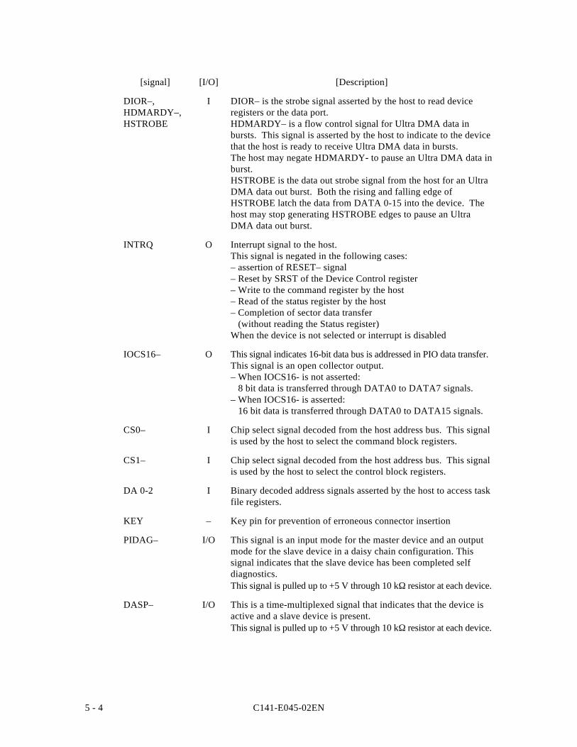
C141-E045-02EN5 - 4
[signal] [I/O] [Description]
DIOR–,HDMARDY–,HSTROBE
I DIOR– is the strobe signal asserted by the host to read deviceregisters or the data port.HDMARDY– is a flow control signal for Ultra DMA data inbursts. This signal is asserted by the host to indicate to the devicethat the host is ready to receive Ultra DMA data in bursts.The host may negate HDMARDY- to pause an Ultra DMA data inburst.HSTROBE is the data out strobe signal from the host for an UltraDMA data out burst. Both the rising and falling edge ofHSTROBE latch the data from DATA 0-15 into the device. Thehost may stop generating HSTROBE edges to pause an UltraDMA data out burst.
INTRQ O Interrupt signal to the host.This signal is negated in the following cases:– assertion of RESET– signal– Reset by SRST of the Device Control register– Write to the command register by the host– Read of the status register by the host– Completion of sector data transfer (without reading the Status register)When the device is not selected or interrupt is disabled
IOCS16– O This signal indicates 16-bit data bus is addressed in PIO data transfer.This signal is an open collector output.– When IOCS16- is not asserted: 8 bit data is transferred through DATA0 to DATA7 signals.– When IOCS16- is asserted: 16 bit data is transferred through DATA0 to DATA15 signals.
CS0– I Chip select signal decoded from the host address bus. This signalis used by the host to select the command block registers.
CS1– I Chip select signal decoded from the host address bus. This signalis used by the host to select the control block registers.
DA 0-2 I Binary decoded address signals asserted by the host to access taskfile registers.
KEY – Key pin for prevention of erroneous connector insertion
PIDAG– I/O This signal is an input mode for the master device and an outputmode for the slave device in a daisy chain configuration. Thissignal indicates that the slave device has been completed selfdiagnostics.This signal is pulled up to +5 V through 10 kΩ resistor at each device.
DASP– I/O This is a time-multiplexed signal that indicates that the device isactive and a slave device is present.This signal is pulled up to +5 V through 10 kΩ resistor at each device.
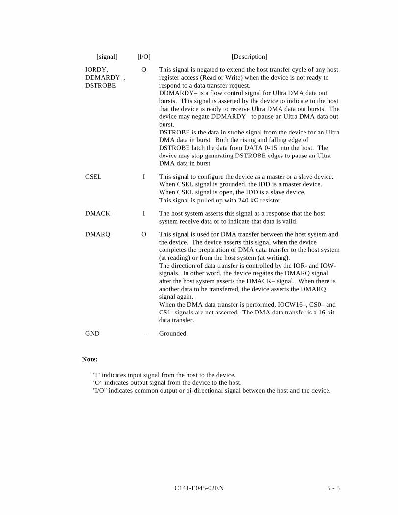
C141-E045-02EN 5 - 5
[signal] [I/O] [Description]
IORDY,DDMARDY–,DSTROBE
O This signal is negated to extend the host transfer cycle of any hostregister access (Read or Write) when the device is not ready torespond to a data transfer request.DDMARDY– is a flow control signal for Ultra DMA data outbursts. This signal is asserted by the device to indicate to the hostthat the device is ready to receive Ultra DMA data out bursts. Thedevice may negate DDMARDY– to pause an Ultra DMA data outburst.DSTROBE is the data in strobe signal from the device for an UltraDMA data in burst. Both the rising and falling edge ofDSTROBE latch the data from DATA 0-15 into the host. Thedevice may stop generating DSTROBE edges to pause an UltraDMA data in burst.
CSEL I This signal to configure the device as a master or a slave device.When CSEL signal is grounded, the IDD is a master device.When CSEL signal is open, the IDD is a slave device.This signal is pulled up with 240 kΩ resistor.
DMACK– I The host system asserts this signal as a response that the hostsystem receive data or to indicate that data is valid.
DMARQ O This signal is used for DMA transfer between the host system andthe device. The device asserts this signal when the devicecompletes the preparation of DMA data transfer to the host system(at reading) or from the host system (at writing).The direction of data transfer is controlled by the IOR- and IOW-signals. In other word, the device negates the DMARQ signalafter the host system asserts the DMACK– signal. When there isanother data to be transferred, the device asserts the DMARQsignal again.When the DMA data transfer is performed, IOCW16–, CS0– andCS1- signals are not asserted. The DMA data transfer is a 16-bitdata transfer.
GND – Grounded
Note:
"I" indicates input signal from the host to the device."O" indicates output signal from the device to the host."I/O" indicates common output or bi-directional signal between the host and the device.
C141-E045-02EN5 - 6
5.2 Logical Interface
The device can operate for command execution in either address-specified mode; cylinder-head-sector (CHS) or Logical block address (LBA) mode. The IDENTIFY DEVICEinformation indicates whether the device supports the LBA mode. When the host systemspecifies the LBA mode by setting bit 6 in the Device/Head register to 1, HS3 to HS0 bits ofthe Device/Head register indicates the head No. under the LBA mode, and all bits of theCylinder High, Cylinder Low, and Sector Number registers are LBA bits.
The sector No. under the LBA mode proceeds in the ascending order with the start point ofLBA0 (defined as follows).
LBA0 = [Cylinder 0, Head 0, Sector 1]
Even if the host system changes the assignment of the CHS mode by the INITIALIZEDEVICE PARAMETER command, the sector LBA address is not changed.
LBA = [((Cylinder No.) × (Number of head) + (Head No.)) × (Number of sector/track)] + (Sector No.) – 1
5.2.1 I/O registers
Communication between the host system and the device is done through input-output (I/O)registers of the device.
These I/O registers can be selected by the coded signals, CS0–, CS1–, and DA0 to DA2 fromthe host system. Table 5.2. shows the coding address and the function of I/O registers.
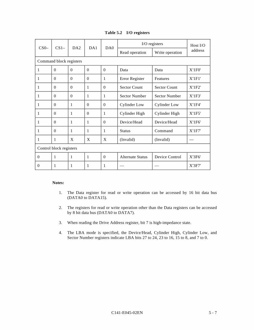
C141-E045-02EN 5 - 7
Table 5.2 I/O registers
I/O registers
Read operation Write operation
Command block registers
1 0 0 0 0 Data Data X'1F0'
1 0 0 0 1 Error Register Features X'1F1'
1 0 0 1 0 Sector Count Sector Count X'1F2'
1 0 0 1 1 Sector Number Sector Number X'1F3'
1 0 1 0 0 Cylinder Low Cylinder Low X'1F4'
1 0 1 0 1 Cylinder High Cylinder High X'1F5'
1 0 1 1 0 Device/Head Device/Head X'1F6'
1 0 1 1 1 Status Command X'1F7'
1 1 X X X (Invalid) (Invalid) —
Control block registers
0 1 1 1 0 Alternate Status Device Control X'3F6'
0 1 1 1 1 — — X'3F7'
Notes:
1. The Data register for read or write operation can be accessed by 16 bit data bus(DATA0 to DATA15).
2. The registers for read or write operation other than the Data registers can be accessedby 8 bit data bus (DATA0 to DATA7).
3. When reading the Drive Address register, bit 7 is high-impedance state.
4. The LBA mode is specified, the Device/Head, Cylinder High, Cylinder Low, andSector Number registers indicate LBA bits 27 to 24, 23 to 16, 15 to 8, and 7 to 0.
Host I/OaddressDA0DA1DA2CS1–CS0–
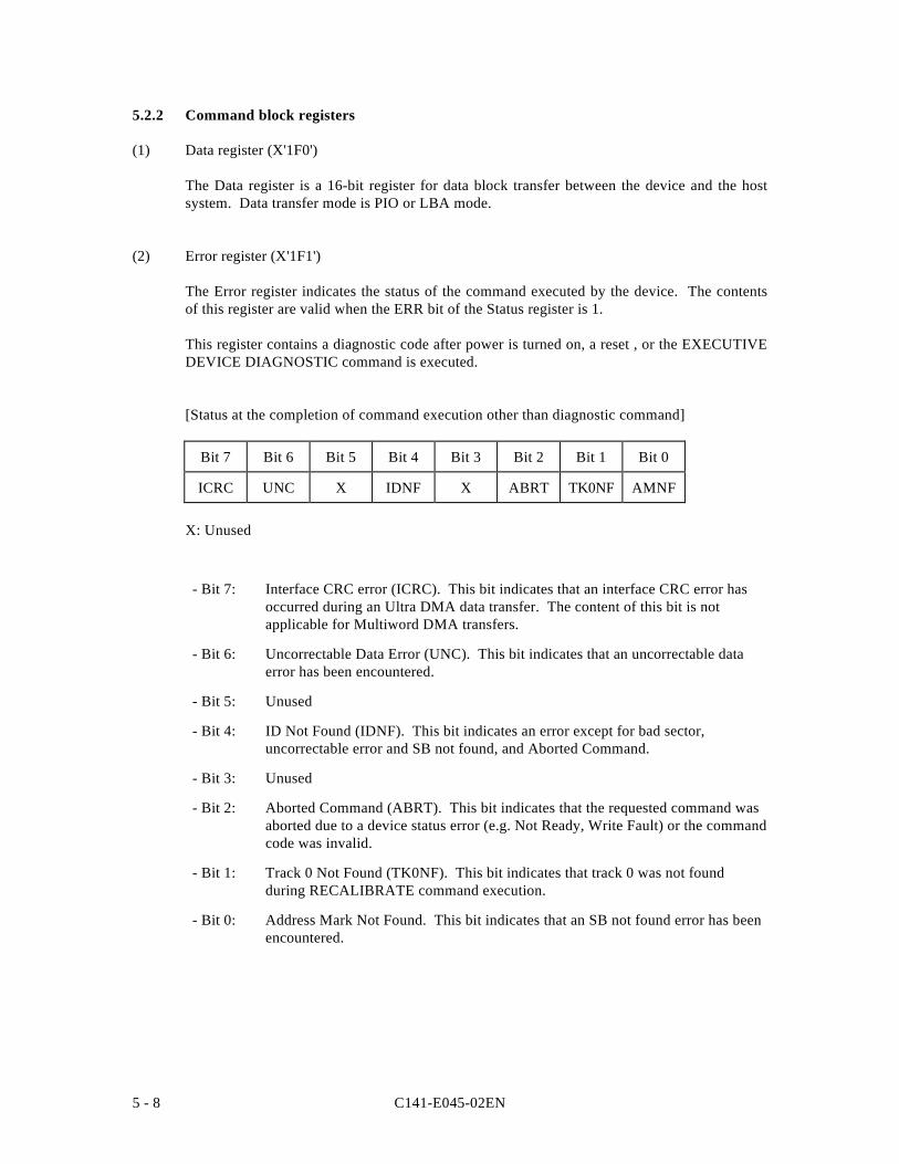
C141-E045-02EN5 - 8
5.2.2 Command block registers
(1) Data register (X'1F0')
The Data register is a 16-bit register for data block transfer between the device and the hostsystem. Data transfer mode is PIO or LBA mode.
(2) Error register (X'1F1')
The Error register indicates the status of the command executed by the device. The contentsof this register are valid when the ERR bit of the Status register is 1.
This register contains a diagnostic code after power is turned on, a reset , or the EXECUTIVEDEVICE DIAGNOSTIC command is executed.
[Status at the completion of command execution other than diagnostic command]
Bit 7 Bit 6 Bit 5 Bit 4 Bit 3 Bit 2 Bit 1 Bit 0
ICRC UNC X IDNF X ABRT TK0NF AMNF
X: Unused
- Bit 7: Interface CRC error (ICRC). This bit indicates that an interface CRC error hasoccurred during an Ultra DMA data transfer. The content of this bit is notapplicable for Multiword DMA transfers.
- Bit 6: Uncorrectable Data Error (UNC). This bit indicates that an uncorrectable dataerror has been encountered.
- Bit 5: Unused
- Bit 4: ID Not Found (IDNF). This bit indicates an error except for bad sector,uncorrectable error and SB not found, and Aborted Command.
- Bit 3: Unused
- Bit 2: Aborted Command (ABRT). This bit indicates that the requested command wasaborted due to a device status error (e.g. Not Ready, Write Fault) or the commandcode was invalid.
- Bit 1: Track 0 Not Found (TK0NF). This bit indicates that track 0 was not foundduring RECALIBRATE command execution.
- Bit 0: Address Mark Not Found. This bit indicates that an SB not found error has beenencountered.
C141-E045-02EN 5 - 9
[Diagnostic code]
X'01': No Error Detected.
X'03': Data Buffer Compare Error.
X'05': ROM Sum Check Error.
X'80': Device 1 (slave device) Failed.Error register of the master device is valid under two devices (master and slave)configuration. If the slave device fails, the master device posts X’80’ OR (thediagnostic code) with its own status (X'01' to X'05').However, when the host system selects the slave device, the diagnostic code of theslave device is posted.
(3) Features register (X'1F1')
The Features register provides specific feature to a command. For instance, it is used with SETFEATURES command to enable or disable caching.
(4) Sector Count register (X'1F2')
The Sector Count register indicates the number of sectors of data to be transferred in a read orwrite operation between the host system and the device. When the value in this register isX'00', the sector count is 256.
When this register indicates X'00' at the completion of the command execution, this indicatesthat the command is completed successfully. If the command is not completed successfully,this register indicates the number of sectors to be transferred to complete the request from thehost system. That is, this register indicates the number of remaining sectors that the data hasnot been transferred due to the error.
The contents of this register has other definition for the following commands; INITIALIZEDEVICE PARAMETERS, FORMAT TRACK, SET FEATURES, IDLE, STANDBY and SETMULTIPLE MODE.
(5) Sector Number register (X'1F3')
The contents of this register indicates the starting sector number for the subsequent command.The sector number should be between X'01' and [the number of sectors per track defined byINITIALIZE DEVICE PARAMETERS command.
Under the LBA mode, this register indicates LBA bits 7 to 0.
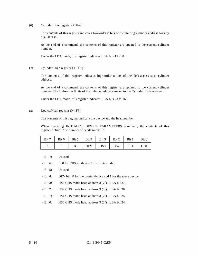
C141-E045-02EN5 - 10
(6) Cylinder Low register (X'1F4')
The contents of this register indicates low-order 8 bits of the starting cylinder address for anydisk-access.
At the end of a command, the contents of this register are updated to the current cylindernumber.
Under the LBA mode, this register indicates LBA bits 15 to 8.
(7) Cylinder High register (X'1F5')
The contents of this register indicates high-order 8 bits of the disk-access start cylinderaddress.
At the end of a command, the contents of this register are updated to the current cylindernumber. The high-order 8 bits of the cylinder address are set to the Cylinder High register.
Under the LBA mode, this register indicates LBA bits 23 to 16.
(8) Device/Head register (X'1F6')
The contents of this register indicate the device and the head number.
When executing INITIALIZE DEVICE PARAMETERS command, the contents of thisregister defines "the number of heads minus 1".
Bit 7 Bit 6 Bit 5 Bit 4 Bit 3 Bit 2 Bit 1 Bit 0
X L X DEV HS3 HS2 HS1 HS0
- Bit 7: Unused
- Bit 6: L. 0 for CHS mode and 1 for LBA mode.
- Bit 5: Unused
- Bit 4: DEV bit. 0 for the master device and 1 for the slave device.
- Bit 3: HS3 CHS mode head address 3 (23). LBA bit 27.
- Bit 2: HS2 CHS mode head address 3 (22). LBA bit 26.
- Bit 1: HS1 CHS mode head address 3 (21). LBA bit 25.
- Bit 0: HS0 CHS mode head address 3 (20). LBA bit 24.
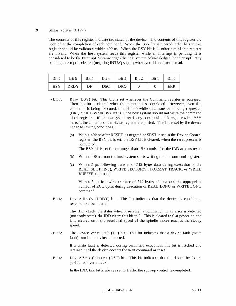
C141-E045-02EN 5 - 11
(9) Status register (X'1F7')
The contents of this register indicate the status of the device. The contents of this register areupdated at the completion of each command. When the BSY bit is cleared, other bits in thisregister should be validated within 400 ns. When the BSY bit is 1, other bits of this registerare invalid. When the host system reads this register while an interrupt is pending, it isconsidered to be the Interrupt Acknowledge (the host system acknowledges the interrupt). Anypending interrupt is cleared (negating INTRQ signal) whenever this register is read.
Bit 7 Bit 6 Bit 5 Bit 4 Bit 3 Bit 2 Bit 1 Bit 0
BSY DRDY DF DSC DRQ 0 0 ERR
- Bit 7: Busy (BSY) bit. This bit is set whenever the Command register is accessed.Then this bit is cleared when the command is completed. However, even if acommand is being executed, this bit is 0 while data transfer is being requested(DRQ bit = 1).When BSY bit is 1, the host system should not write the commandblock registers. If the host system reads any command block register when BSYbit is 1, the contents of the Status register are posted. This bit is set by the deviceunder following conditions:
(a) Within 400 ns after RESET- is negated or SRST is set in the Device Controlregister, the BSY bit is set. the BSY bit is cleared, when the reset process iscompleted.The BSY bit is set for no longer than 15 seconds after the IDD accepts reset.
(b) Within 400 ns from the host system starts writing to the Command register.
(c) Within 5 µs following transfer of 512 bytes data during execution of theREAD SECTOR(S), WRITE SECTOR(S), FORMAT TRACK, or WRITEBUFFER command.
Within 5 µs following transfer of 512 bytes of data and the appropriatenumber of ECC bytes during execution of READ LONG or WRITE LONGcommand.
- Bit 6: Device Ready (DRDY) bit. This bit indicates that the device is capable torespond to a command.
The IDD checks its status when it receives a command. If an error is detected(not ready state), the IDD clears this bit to 0. This is cleared to 0 at power-on andit is cleared until the rotational speed of the spindle motor reaches the steadyspeed.
- Bit 5: The Device Write Fault (DF) bit. This bit indicates that a device fault (writefault) condition has been detected.
If a write fault is detected during command execution, this bit is latched andretained until the device accepts the next command or reset.
- Bit 4: Device Seek Complete (DSC) bit. This bit indicates that the device heads arepositioned over a track.
In the IDD, this bit is always set to 1 after the spin-up control is completed.
C141-E045-02EN5 - 12
- Bit 3: Data Request (DRQ) bit. This bit indicates that the device is ready to transferdata of word unit or byte unit between the host system and the device.
- Bit 2: Always 0.
- Bit 1: Always 0.
- Bit 0: Error (ERR) bit. This bit indicates that an error was detected while the previouscommand was being executed. The Error register indicates the additionalinformation of the cause for the error.
(10) Command register (X'1F7')
The Command register contains a command code being sent to the device. After this registeris written, the command execution starts immediately.
Table 5.3 lists the executable commands and their command codes. This table also lists thenecessary parameters for each command which are written to certain registers before theCommand register is written.
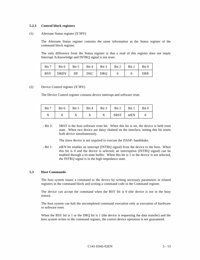
C141-E045-02EN 5 - 13
5.2.3 Control block registers
(1) Alternate Status register (X'3F6')
The Alternate Status register contains the same information as the Status register of thecommand block register.
The only difference from the Status register is that a read of this register does not implyInterrupt Acknowledge and INTRQ signal is not reset.
Bit 7 Bit 6 Bit 5 Bit 4 Bit 3 Bit 2 Bit 1 Bit 0
BSY DRDY DF DSC DRQ 0 0 ERR
(2) Device Control register (X'3F6')
The Device Control register contains device interrupt and software reset.
Bit 7 Bit 6 Bit 5 Bit 4 Bit 3 Bit 2 Bit 1 Bit 0
X X X X X SRST nIEN 0
- Bit 2: SRST is the host software reset bit. When this bit is set, the device is held resetstate. When two device are daisy chained on the interface, setting this bit resetsboth device simultaneously.
The slave device is not required to execute the DASP- handshake.
- Bit 1: nIEN bit enables an interrupt (INTRQ signal) from the device to the host. Whenthis bit is 0 and the device is selected, an interruption (INTRQ signal) can beenabled through a tri-state buffer. When this bit is 1 or the device is not selected,the INTRQ signal is in the high-impedance state.
5.3 Host Commands
The host system issues a command to the device by writing necessary parameters in relatedregisters in the command block and writing a command code in the Command register.
The device can accept the command when the BSY bit is 0 (the device is not in the busystatus).
The host system can halt the uncompleted command execution only at execution of hardwareor software reset.
When the BSY bit is 1 or the DRQ bit is 1 (the device is requesting the data transfer) and thehost system writes to the command register, the correct device operation is not guaranteed.
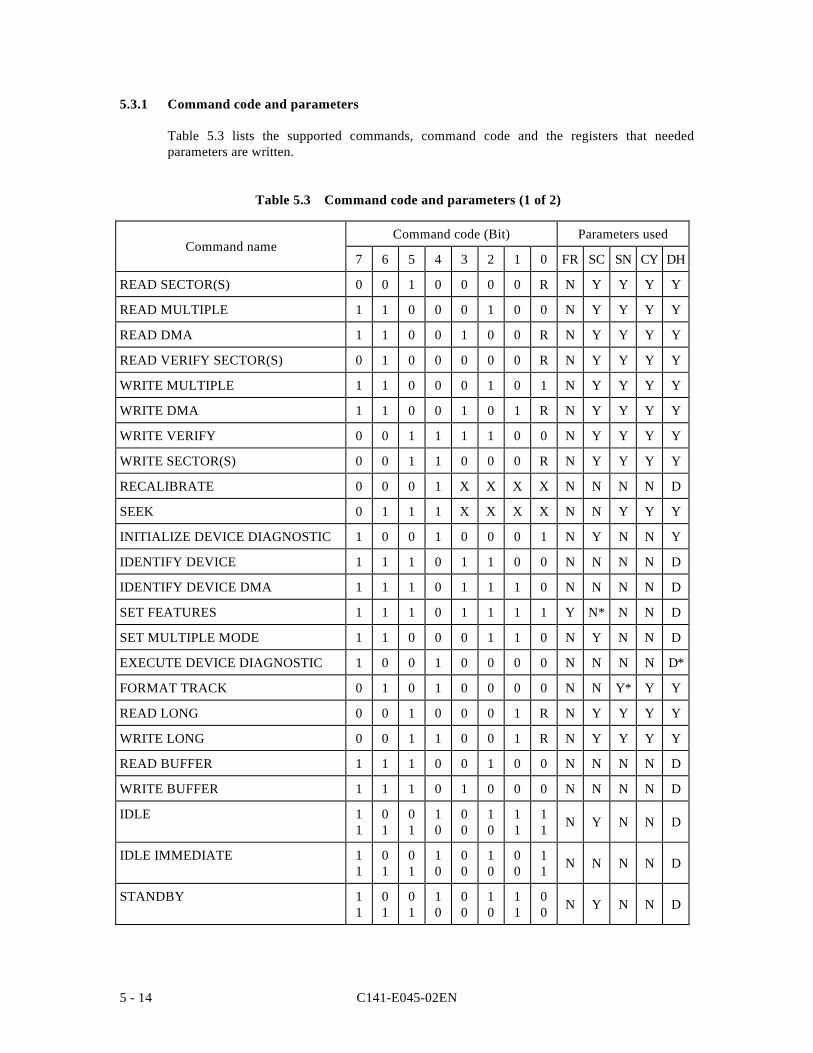
C141-E045-02EN5 - 14
5.3.1 Command code and parameters
Table 5.3 lists the supported commands, command code and the registers that neededparameters are written.
Table 5.3 Command code and parameters (1 of 2)
Command code (Bit) Parameters used
7 6 5 4 3 2 1 0 FR SC SN CY DH
READ SECTOR(S) 0 0 1 0 0 0 0 R N Y Y Y Y
READ MULTIPLE 1 1 0 0 0 1 0 0 N Y Y Y Y
READ DMA 1 1 0 0 1 0 0 R N Y Y Y Y
READ VERIFY SECTOR(S) 0 1 0 0 0 0 0 R N Y Y Y Y
WRITE MULTIPLE 1 1 0 0 0 1 0 1 N Y Y Y Y
WRITE DMA 1 1 0 0 1 0 1 R N Y Y Y Y
WRITE VERIFY 0 0 1 1 1 1 0 0 N Y Y Y Y
WRITE SECTOR(S) 0 0 1 1 0 0 0 R N Y Y Y Y
RECALIBRATE 0 0 0 1 X X X X N N N N D
SEEK 0 1 1 1 X X X X N N Y Y Y
INITIALIZE DEVICE DIAGNOSTIC 1 0 0 1 0 0 0 1 N Y N N Y
IDENTIFY DEVICE 1 1 1 0 1 1 0 0 N N N N D
IDENTIFY DEVICE DMA 1 1 1 0 1 1 1 0 N N N N D
SET FEATURES 1 1 1 0 1 1 1 1 Y N* N N D
SET MULTIPLE MODE 1 1 0 0 0 1 1 0 N Y N N D
EXECUTE DEVICE DIAGNOSTIC 1 0 0 1 0 0 0 0 N N N N D*
FORMAT TRACK 0 1 0 1 0 0 0 0 N N Y* Y Y
READ LONG 0 0 1 0 0 0 1 R N Y Y Y Y
WRITE LONG 0 0 1 1 0 0 1 R N Y Y Y Y
READ BUFFER 1 1 1 0 0 1 0 0 N N N N D
WRITE BUFFER 1 1 1 0 1 0 0 0 N N N N D
IDLE 11
01
01
10
00
10
11
11 N Y N N D
IDLE IMMEDIATE 11
01
01
10
00
10
00
11 N N N N D
STANDBY 11
01
01
10
00
10
11
00 N Y N N D
Command name
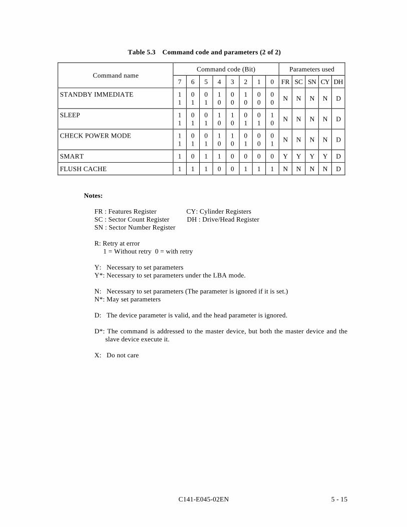
C141-E045-02EN 5 - 15
Table 5.3 Command code and parameters (2 of 2)
Command code (Bit) Parameters used
7 6 5 4 3 2 1 0 FR SC SN CY DH
STANDBY IMMEDIATE 11
01
01
10
00
10
00
00 N N N N D
SLEEP 11
01
01
10
10
01
01
10 N N N N D
CHECK POWER MODE 11
01
01
10
10
01
00
01 N N N N D
SMART 1 0 1 1 0 0 0 0 Y Y Y Y D
FLUSH CACHE 1 1 1 0 0 1 1 1 N N N N D
Notes:
FR : Features Register CY: Cylinder RegistersSC : Sector Count Register DH : Drive/Head RegisterSN : Sector Number Register
R: Retry at error 1 = Without retry 0 = with retry
Y: Necessary to set parametersY*: Necessary to set parameters under the LBA mode.
N: Necessary to set parameters (The parameter is ignored if it is set.)N*: May set parameters
D: The device parameter is valid, and the head parameter is ignored.
D*: The command is addressed to the master device, but both the master device and theslave device execute it.
X: Do not care
Command name
C141-E045-02EN5 - 16
5.3.2 Command descriptions
The contents of the I/O registers to be necessary for issuing a command and the exampleindication of the I/O registers at command completion are shown as following in thissubsection.
Example: READ SECTOR(S) WITH RETRY
At command issuance (I/O registers setting contents)
Bit 7 6 5 4 3 2 1 0
1F7H(CM) 0 0 1 0 0 0 0 0
1F6H(DH) × L × DV Head No. / LBA [MSB]
1F5H(CH) Start cylinder address [MSB] / LBA
1F4H(CL) Start cylinder address [LSB] / LBA
1F3H(SN) Start sector No. / LBA [LSB]
1F2H(SC) Transfer sector count
1F1H(FR) xx
At command completion (I/O registers contents to be read)
Bit 7 6 5 4 3 2 1 0
1F7H(ST) Error information
1F6H(DH) × L × DV Head No. / LBA [MSB]
1F5H(CH) Start cylinder address [MSB] / LBA
1F4H(CL) Start cylinder address [LSB] / LBA
1F3H(SN) Start sector No. / LBA [LSB]
1F2H(SC) X‘00’
1F1H(ER) Error information
CM: Command register FR: Features registerDH: Device/Head register ST: Status registerCH: Cylinder High register ER: Error registerCL: Cylinder Low register L: LBA (logical block address) setting bitSN: Sector Number register DV: Device address. bitSC: Sector Count register x, xx: Do not care (no necessary to set)
C141-E045-02EN 5 - 17
Note:
1. When the L bit is specified to 1, the lower 4 bits of the DH register and all bits of theCH, CL and SN registers indicate the LBA bits (bits of the DH register are the MSB(most significant bit) and bits of the SN register are the LSB (least significant bit).
2. At error occurrence, the SC register indicates the remaining sector count of data transfer.
3. In the table indicating I/O registers contents in this subsection, bit indication is omitted.
(1) READ SECTOR(S) (X'20' or X'21')
This command reads data of sectors specified in the Sector Count register from the address specifiedin the Device/Head, Cylinder High, Cylinder Low and Sector Number registers. Number of sectorscan be specified to 256 sectors in maximum. To specify 256 sectors reading, '00' is specified. Forthe DRQ, INTRQ, and BSY protocols related to data transfer, see Subsection 4.4.1.
If the head is not on the track specified by the host, the device performs a implied seek. Afterthe head reaches to the specified track, the device reads the target sector.
The DRQ bit of the Status register is always set prior to the data transfer regardless of an errorcondition.
Upon the completion of the command execution, command block registers contain thecylinder, head, and sector addresses (in the CHS mode) or logical block address (in the LBAmode) of the last sector read.
If an error occurs in a sector, the read operation is terminated at the sector where the error occurred.
Command block registers contain the cylinder, the head, and the sector addresses of the sector(in the CHS mode) or the logical block address (in the LBA mode) where the error occurred,and remaining number of sectors of which data was not transferred.
At command issuance (I/O registers setting contents)
1F7H(CM) 0 0 1 0 0 0 0 R
1F6H(DH) × L × DV Start head No. /LBA [MSB]
1F5H(CH)1F4H(CL)1F3H(SN)1F2H(SC)1F1H(FR)
Start cylinder No. [MSB]/ LBAStart cylinder No. [LSB] / LBAStart sector No. / LBA [LSB] Transfer sector count xx
R = 0 →with RetryR = 1 →without Retry
C141-E045-02EN5 - 18
At command completion (I/O registers contents to be read)
1F7H(ST) Status information
1F6H(DH) × L × DV End head No. /LBA [MSB]
1F5H(CH)1F4H(CL)1F3H(SN)1F2H(SC)1F1H(ER)
End cylinder No. [MSB] / LBAEnd cylinder No. [LSB] / LBAEnd sector No. / LBA [LSB] 00 (*1) Error information
*1 If the command is terminated due to an error, the remaining number ofsectors of which data was not transferred is set in this register.
(2) READ MULTIPLE (X'C4')
This command operates similarly to the READ SECTOR(S) command. The device does notgenerate an interrupt (assertion of the INTRQ signal) on each every sector. An interrupt isgenerated after the transfer of a block of sectors for which the number is specified by the SETMULTIPLE MODE command.
The implementation of the READ MULTIPLE command is identical to that of the READSECTOR(S) command except that the number of sectors is specified by the SET MULTIPLEMODE command are transferred without intervening interrupts. In the READ MULTIPLEcommand operation, the DRQ bit of the Status register is set only at the start of the data block,and is not set on each sector.
The number of sectors (block count) to be transferred without interruption is specified by theSET MULTIPLE MODE command. The SET MULTIPLE MODE command should beexecuted prior to the READ MULTIPLE command.
When the READ MULTIPLE command is issued, the Sector Count register contains the number ofsectors requested (not a number of the block count or a number of sectors in a block).
Upon receipt of this command, the device executes this command even if the value of the SectorCount register is less than the defined block count (the value of the Sector Count should not be 0).
If the number of requested sectors is not divided evenly (having the same number of sectors[block count]), as many full blocks as possible are transferred, then a final partial block istransferred. The number of sectors in the partial block to be transferred is n where n =remainder of ("number of sectors"/"block count").
If the READ MULTIPLE command is issued before the SET MULTIPLE MODE command isexecuted or when the READ MULTIPLE command is disabled, the device rejects the READMULTIPLE command with an ABORTED COMMAND error.
If an error occurs, reading sector is stopped at the sector where the error occurred. Commandblock registers contain the cylinder, the head, the sector addresses (in the CHS mode) or thelogical block address (in the LBA mode) of the sector where the error occurred, and remainingnumber of sectors that had not transferred after the sector where the error occurred.
An interrupt is generated when the DRQ bit is set at the beginning of each block or a partial block.
C141-E045-02EN 5 - 19
Figure 5.2 shows an example of the execution of the READ MULTIPLE command.
• Block count specified by SET MULTIPLE MODE command = 4 (number of sectors in ablock)
• READ MULTIPLE command specifies;Number of requested sectors = 9 (Sector Count register = 9)↓Number of sectors in incomplete block = remainder of 9/4 =1
Status readStatus readStatus read
Command Issue
BSY
INTRQ
DRDY
~ParameterWrite
95 6 7 81 2 3 4PartialblockBlockBlock
Sectortransferred
DRQ
Figure 5.2 Execution example of READ MULTIPLE command
At command issuance (I/O registers setting contents)
1F7H(CM) 1 1 0 0 0 1 0 0
1F6H(DH) × L × DV Start head No. /LBA [MSB]
1F5H(CH)1F4H(CL)1F3H(SN)1F2H(SC)1F1H(FR)
Start cylinder No. [MSB]/ LBAStart cylinder No. [LSB] / LBAStart sector No. / LBA [LSB] Transfer sector count xx
At command completion (I/O registers contents to be read)
1F7H(ST) Status information
1F6H(DH) × L × DV End head No. /LBA [MSB]
1F5H(CH)1F4H(CL)1F3H(SN)1F2H(SC)1F1H(ER)
End cylinder No. [MSB] / LBAEnd cylinder No. [LSB] / LBAEnd sector No. / LBA [LSB] 00H
Error information
C141-E045-02EN5 - 20
Note:
If the command is terminated due to an error, the remaining number of sectors for whichdata was not transferred is set in this register.
(3) READ DMA (X'C8' or X'C9')
This command operates similarly to the READ SECTOR(S) command except for followingevents.
• The data transfer starts at the timing of DMARQ signal assertion.
• The device controls the assertion or negation timing of the DMARQ signal.
• The device posts a status as the result of command execution only once at completion ofthe data transfer.
When an error, such as an unrecoverable medium error, that the command execution cannot becontinued is detected, the data transfer is stopped without transferring data of sectors after the erredsector. The device generates an interrupt using the INTRQ signal and posts a status to the hostsystem. The format of the error information is the same as the READ SECTOR(S) command.
In LBA mode
The logical block address is specified using the start head No., start cylinder No., and firstsector No. fields. At command completion, the logical block address of the last sector andremaining number of sectors of which data was not transferred, like in the CHS mode, are set.
The host system can select the DMA transfer mode by using the SET FEATURES command.
1) Single word DMA transfer mode 2:Sets the FR register = X'03' and SC register = X'12' by the SET FEATURES command
2) Multiword DMA transfer mode 2:Sets the FR register = X'03' and SC register = X'22' by the SET FEATURES command
3) Ultra DMA transfer mode 2:Sets the FR register = X'03' and SC register = X'42' by the SET FEATURES command
At command issuance (I/O registers setting contents)
1F7H(CM) 1 1 0 0 1 0 0 R
1F6H(DH) × L × DV Start head No. /LBA [MSB]
1F5H(CH)1F4H(CL)1F3H(SN)1F2H(SC)1F1H(FR)
Start cylinder No. [MSB]/ LBAStart cylinder No. [LSB] / LBAStart sector No. / LBA [LSB] Transfer sector count xx
R = 0 → with RetryR = 1 → without Retry
C141-E045-02EN 5 - 21
At command completion (I/O registers contents to be read)
1F7H(ST) Status information
1F6H(DH) × L × DV End head No. /LBA [MSB]
1F5H(CH)1F4H(CL)1F3H(SN)1F2H(SC)1F1H(ER)
End cylinder No. [MSB] / LBAEnd cylinder No. [LSB] / LBAEnd sector No. / LBA [LSB] 00 (*1) Error information
*1 If the command is terminated due to an error, the remaining number ofsectors of which data was not transferred is set in this register.
(4) READ VERIFY SECTOR(S) (X'40' or X'41')
This command operates similarly to the READ SECTOR(S) command except that the data isnot transferred to the host system.
After all requested sectors are verified, the device clears the BSY bit of the Status register andgenerates an interrupt. Upon the completion of the command execution, the command blockregisters contain the cylinder, head, and sector number of the last sector verified.
If an error occurs, the verify operation is terminated at the sector where the error occurred. Thecommand block registers contain the cylinder, the head, and the sector addresses (in the CHSmode) or the logical block address (in the LBA mode) of the sector where the error occurred.The Sector Count register indicates the number of sectors that have not been verified.
If a correctable error is found, the device sets the CORR bit of the Status register to 1 after thecommand is completed (before the device generates an interrupt).
At command issuance (I/O registers setting contents)
1F7H(CM) 0 1 0 0 0 0 0 R
1F6H(DH) × L × DV Start head No. /LBA [MSB]
1F5H(CH)1F4H(CL)1F3H(SN)1F2H(SC)1F1H(FR)
Start cylinder No. [MSB]/ LBAStart cylinder No. [LSB] / LBAStart sector No. / LBA [LSB] Transfer sector count xx
R = 0 →with RetryR = 1 →without Retry
C141-E045-02EN5 - 22
At command completion (I/O registers contents to be read)
1F7H(ST) Status information
1F6H(DH) × L × DV End head No. /LBA [MSB]
1F5H(CH)1F4H(CL)1F3H(SN)1F2H(SC)1F1H(ER)
End cylinder No. [MSB] / LBAEnd cylinder No. [LSB] / LBAEnd sector No. / LBA [LSB] 00 (*1) Error information
*1 If the command is terminated due to an error, the remaining number ofsectors of which data was not transferred is set in this register.
(5) WRITE SECTOR(S) (X'30' or X'31')
This command writes data of sectors from the address specified in the Device/Head, CylinderHigh, Cylinder Low, and Sector Number registers to the address specified in the Sector Countregister. Number of sectors can be specified to 256 sectors in maximum. Data transfer beginsat the sector specified in the Sector Number register. For the DRQ, INTRQ, and BSYprotocols related to data transfer, see Subsection 4.4.2.
If the head is not on the track specified by the host, the device performs a implied seek. Afterthe head reaches to the specified track, the device writes the target sector.
The data stored in the buffer, and CRC code and ECC bytes are written to the data field of thecorresponding sector(s). Upon the completion of the command execution, the command blockregisters contain the cylinder, head, and sector addresses of the last sector written.
If an error occurs during multiple sector write operation, the write operation is terminated atthe sector where the error occurred. Command block registers contain the cylinder, the head,the sector addresses (in the CHS mode) or the logical block address (in the LBA mode) of thesector where the error occurred. Then the host can read the command block registers todetermine what error has occurred and on which sector the error has occurred.
At command issuance (I/O registers setting contents)
1F7H(CM) 0 0 1 1 0 0 0 R
1F6H(DH) × L × DV Start head No. /LBA [MSB]
1F5H(CH)1F4H(CL)1F3H(SN)1F2H(SC)1F1H(FR)
Start cylinder No. [MSB]/ LBAStart cylinder No. [LSB] / LBAStart sector No. / LBA [LSB] Transfer sector count xx
R = 0 →with RetryR = 1 →without Retry
C141-E045-02EN 5 - 23
At command completion (I/O registers contents to be read)
1F7H(ST) Status information
1F6H(DH) × L × DV End head No. /LBA [MSB]
1F5H(CH)1F4H(CL)1F3H(SN)1F2H(SC)1F1H(ER)
End cylinder No. [MSB] / LBAEnd cylinder No. [LSB] / LBAEnd sector No. / LBA [LSB] 00 (*1) Error information
*1 If the command is terminated due to an error, the remaining number ofsectors of which data was not transferred is set in this register.
(6) WRITE MULTIPLE (X'C5')
This command is similar to the WRITE SECTOR(S) command. The device does not generateinterrupts (assertion of the INTRQ) signal) on each sector but on the transfer of a block whichcontains the number of sectors for which the number is defined by the SET MULTIPLEMODE command.
The implementation of the WRITE MULTIPLE command is identical to that of the WRITESECTOR(S) command except that the number of sectors is specified by the SET MULTIPLEMODE command are transferred without intervening interrupts. In the WRITE MULTIPLEcommand operation, the DRQ bit of the Status register is required to set only at the start of thedata block, not on each sector.
The number of sectors (block count) to be transferred without interruption is specified by theSET MULTIPLE MODE command. The SET MULTIPLE MODE command should beexecuted prior to the WRITE MULTIPLE command.
When the WRITE MULTIPLE command is issued, the Sector Count register contains the numberof sectors requested (not a number of the block count or a number of sectors in a block).
Upon receipt of this command, the device executes this command even if the value of the SectorCount register is less than the defined block count the value of the Sector Count should not be 0).
If the number of requested sectors is not divided evenly (having the same number of sectors[block count]), as many full blocks as possible are transferred, then a final partial block istransferred. The number of sectors in the partial block to be transferred is n where n =remainder of ("number of sectors"/"block count").
If the WRITE MULTIPLE command is issued before the SET MULTIPLE MODE commandis executed or when WRITE MULTIPLE command is disabled, the device rejects the WRITEMULTIPLE command with an ABORTED COMMAND error.
Disk errors encountered during execution of the WRITE MULTIPLE command are posted afterattempting to write the block or the partial block that was transferred. Write operation ends at thesector where the error was encountered even if the sector is in the middle of a block. If an erroroccurs, the subsequent block shall not be transferred. Interrupts are generated when the DRQ bit ofthe Status register is set at the beginning of each block or partial block.
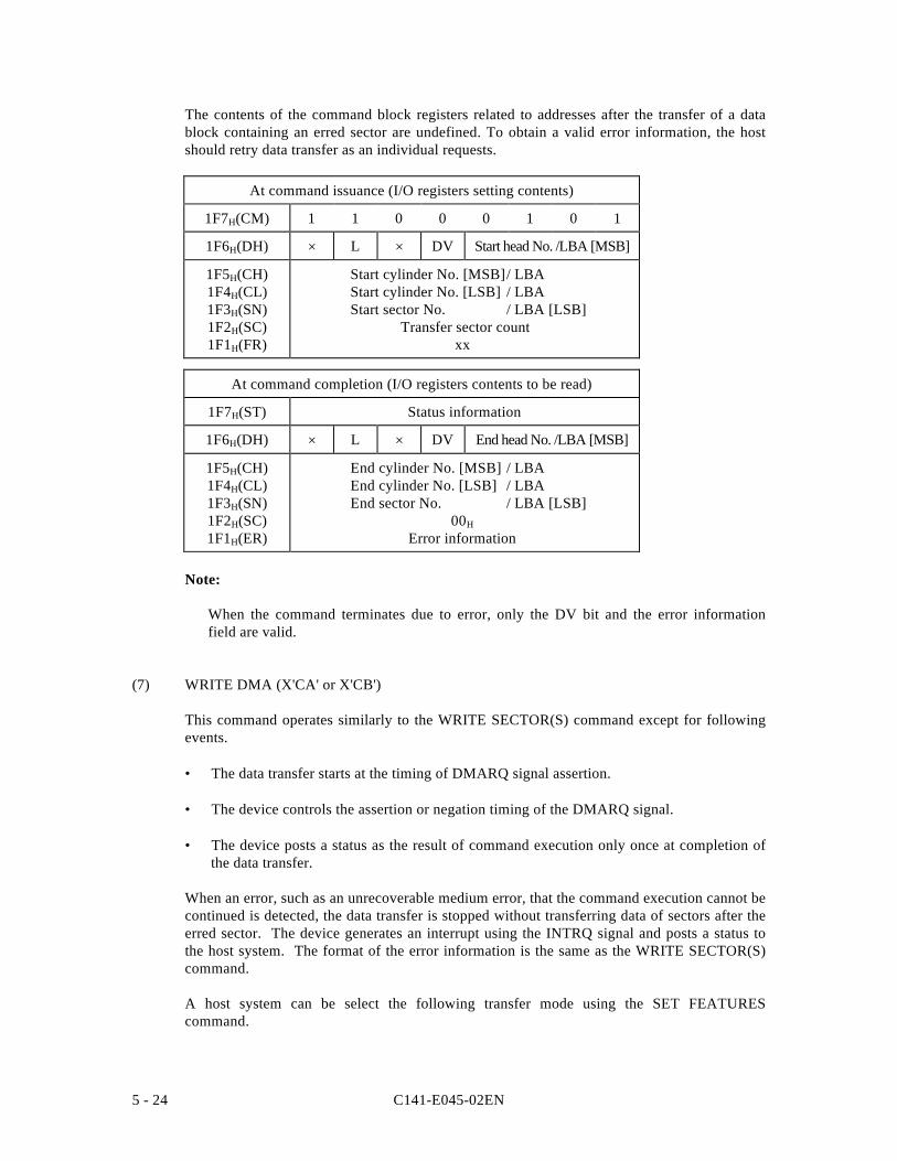
C141-E045-02EN5 - 24
The contents of the command block registers related to addresses after the transfer of a datablock containing an erred sector are undefined. To obtain a valid error information, the hostshould retry data transfer as an individual requests.
At command issuance (I/O registers setting contents)
1F7H(CM) 1 1 0 0 0 1 0 1
1F6H(DH) × L × DV Start head No. /LBA [MSB]
1F5H(CH)1F4H(CL)1F3H(SN)1F2H(SC)1F1H(FR)
Start cylinder No. [MSB]/ LBAStart cylinder No. [LSB] / LBAStart sector No. / LBA [LSB] Transfer sector count xx
At command completion (I/O registers contents to be read)
1F7H(ST) Status information
1F6H(DH) × L × DV End head No. /LBA [MSB]
1F5H(CH)1F4H(CL)1F3H(SN)1F2H(SC)1F1H(ER)
End cylinder No. [MSB] / LBAEnd cylinder No. [LSB] / LBAEnd sector No. / LBA [LSB] 00H
Error information
Note:
When the command terminates due to error, only the DV bit and the error informationfield are valid.
(7) WRITE DMA (X'CA' or X'CB')
This command operates similarly to the WRITE SECTOR(S) command except for followingevents.
• The data transfer starts at the timing of DMARQ signal assertion.
• The device controls the assertion or negation timing of the DMARQ signal.
• The device posts a status as the result of command execution only once at completion ofthe data transfer.
When an error, such as an unrecoverable medium error, that the command execution cannot becontinued is detected, the data transfer is stopped without transferring data of sectors after theerred sector. The device generates an interrupt using the INTRQ signal and posts a status tothe host system. The format of the error information is the same as the WRITE SECTOR(S)command.
A host system can be select the following transfer mode using the SET FEATUREScommand.
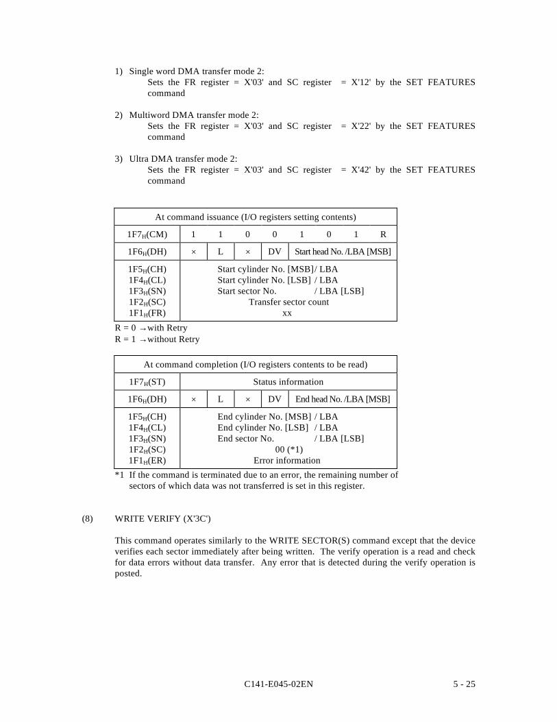
C141-E045-02EN 5 - 25
1) Single word DMA transfer mode 2:Sets the FR register = X'03' and SC register = X'12' by the SET FEATUREScommand
2) Multiword DMA transfer mode 2:Sets the FR register = X'03' and SC register = X'22' by the SET FEATUREScommand
3) Ultra DMA transfer mode 2:Sets the FR register = X'03' and SC register = X'42' by the SET FEATUREScommand
At command issuance (I/O registers setting contents)
1F7H(CM) 1 1 0 0 1 0 1 R
1F6H(DH) × L × DV Start head No. /LBA [MSB]
1F5H(CH)1F4H(CL)1F3H(SN)1F2H(SC)1F1H(FR)
Start cylinder No. [MSB]/ LBAStart cylinder No. [LSB] / LBAStart sector No. / LBA [LSB] Transfer sector count xx
R = 0 →with RetryR = 1 →without Retry
At command completion (I/O registers contents to be read)
1F7H(ST) Status information
1F6H(DH) × L × DV End head No. /LBA [MSB]
1F5H(CH)1F4H(CL)1F3H(SN)1F2H(SC)1F1H(ER)
End cylinder No. [MSB] / LBAEnd cylinder No. [LSB] / LBAEnd sector No. / LBA [LSB] 00 (*1) Error information
*1 If the command is terminated due to an error, the remaining number ofsectors of which data was not transferred is set in this register.
(8) WRITE VERIFY (X'3C')
This command operates similarly to the WRITE SECTOR(S) command except that the deviceverifies each sector immediately after being written. The verify operation is a read and checkfor data errors without data transfer. Any error that is detected during the verify operation isposted.
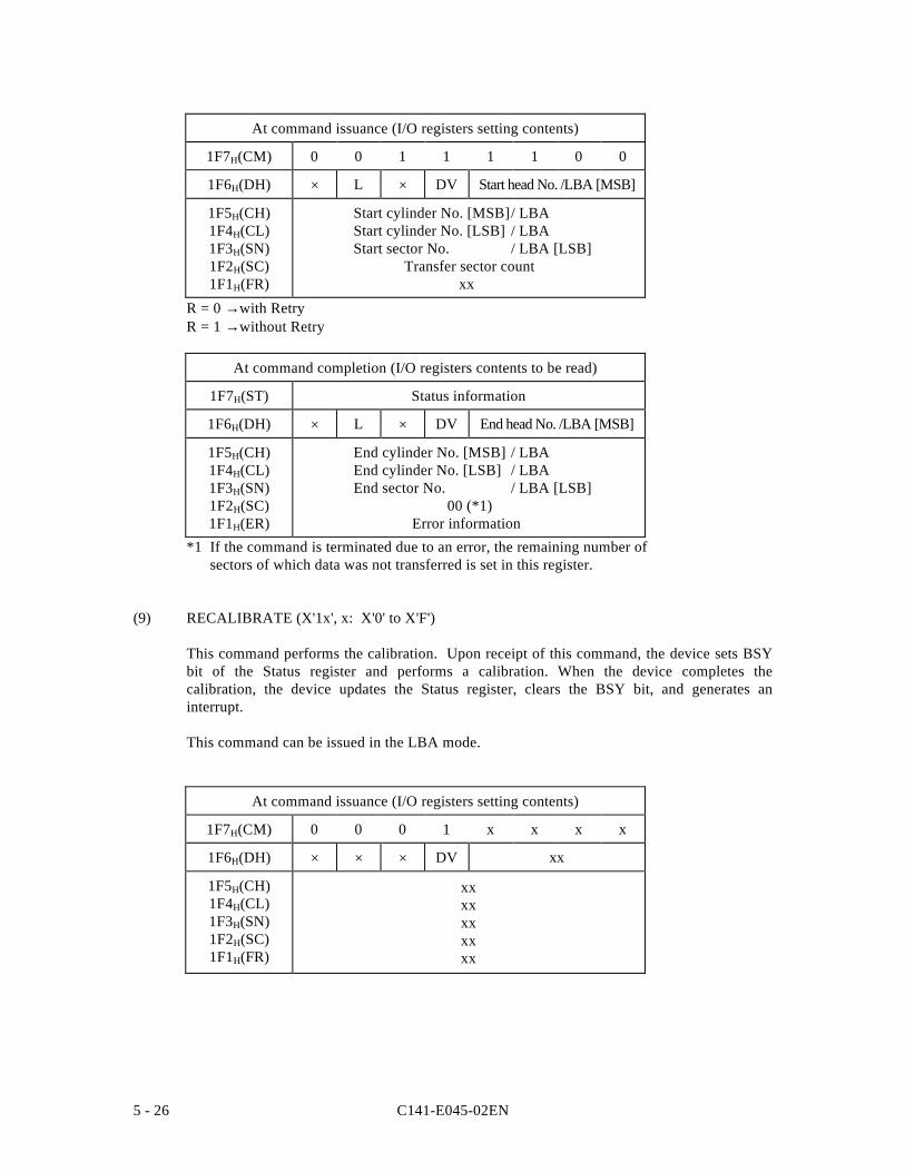
C141-E045-02EN5 - 26
At command issuance (I/O registers setting contents)
1F7H(CM) 0 0 1 1 1 1 0 0
1F6H(DH) × L × DV Start head No. /LBA [MSB]
1F5H(CH)1F4H(CL)1F3H(SN)1F2H(SC)1F1H(FR)
Start cylinder No. [MSB]/ LBAStart cylinder No. [LSB] / LBAStart sector No. / LBA [LSB] Transfer sector count xx
R = 0 →with RetryR = 1 →without Retry
At command completion (I/O registers contents to be read)
1F7H(ST) Status information
1F6H(DH) × L × DV End head No. /LBA [MSB]
1F5H(CH)1F4H(CL)1F3H(SN)1F2H(SC)1F1H(ER)
End cylinder No. [MSB] / LBAEnd cylinder No. [LSB] / LBAEnd sector No. / LBA [LSB] 00 (*1) Error information
*1 If the command is terminated due to an error, the remaining number ofsectors of which data was not transferred is set in this register.
(9) RECALIBRATE (X'1x', x: X'0' to X'F')
This command performs the calibration. Upon receipt of this command, the device sets BSYbit of the Status register and performs a calibration. When the device completes thecalibration, the device updates the Status register, clears the BSY bit, and generates aninterrupt.
This command can be issued in the LBA mode.
At command issuance (I/O registers setting contents)
1F7H(CM) 0 0 0 1 x x x x
1F6H(DH) × × × DV xx
1F5H(CH)1F4H(CL)1F3H(SN)1F2H(SC)1F1H(FR)
xxxxxxxxxx
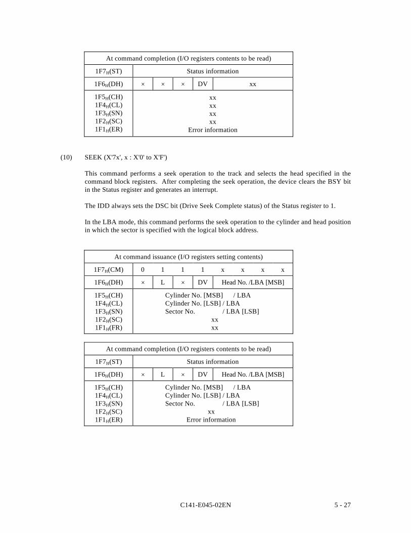
C141-E045-02EN 5 - 27
At command completion (I/O registers contents to be read)
1F7H(ST) Status information
1F6H(DH) × × × DV xx
1F5H(CH)1F4H(CL)1F3H(SN)1F2H(SC)1F1H(ER)
xxxxxxxx
Error information
(10) SEEK (X'7x', x : X'0' to X'F')
This command performs a seek operation to the track and selects the head specified in thecommand block registers. After completing the seek operation, the device clears the BSY bitin the Status register and generates an interrupt.
The IDD always sets the DSC bit (Drive Seek Complete status) of the Status register to 1.
In the LBA mode, this command performs the seek operation to the cylinder and head positionin which the sector is specified with the logical block address.
At command issuance (I/O registers setting contents)
1F7H(CM) 0 1 1 1 x x x x
1F6H(DH) × L × DV Head No. /LBA [MSB]
1F5H(CH)1F4H(CL)1F3H(SN)1F2H(SC)1F1H(FR)
Cylinder No. [MSB] / LBACylinder No. [LSB] / LBASector No. / LBA [LSB] xx xx
At command completion (I/O registers contents to be read)
1F7H(ST) Status information
1F6H(DH) × L × DV Head No. /LBA [MSB]
1F5H(CH)1F4H(CL)1F3H(SN)1F2H(SC)1F1H(ER)
Cylinder No. [MSB] / LBACylinder No. [LSB] / LBASector No. / LBA [LSB] xx Error information
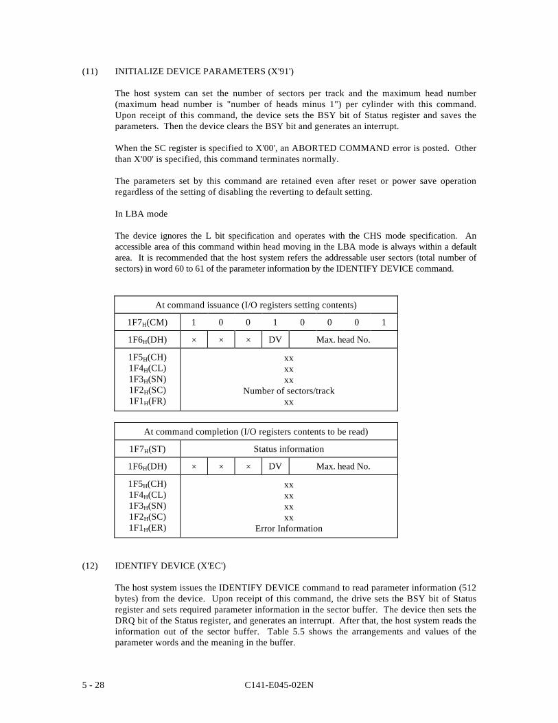
C141-E045-02EN5 - 28
(11) INITIALIZE DEVICE PARAMETERS (X'91')
The host system can set the number of sectors per track and the maximum head number(maximum head number is "number of heads minus 1") per cylinder with this command.Upon receipt of this command, the device sets the BSY bit of Status register and saves theparameters. Then the device clears the BSY bit and generates an interrupt.
When the SC register is specified to X'00', an ABORTED COMMAND error is posted. Otherthan X'00' is specified, this command terminates normally.
The parameters set by this command are retained even after reset or power save operationregardless of the setting of disabling the reverting to default setting.
In LBA mode
The device ignores the L bit specification and operates with the CHS mode specification. Anaccessible area of this command within head moving in the LBA mode is always within a defaultarea. It is recommended that the host system refers the addressable user sectors (total number ofsectors) in word 60 to 61 of the parameter information by the IDENTIFY DEVICE command.
At command issuance (I/O registers setting contents)
1F7H(CM) 1 0 0 1 0 0 0 1
1F6H(DH) × × × DV Max. head No.
1F5H(CH)1F4H(CL)1F3H(SN)1F2H(SC)1F1H(FR)
xxxxxx
Number of sectors/trackxx
At command completion (I/O registers contents to be read)
1F7H(ST) Status information
1F6H(DH) × × × DV Max. head No.
1F5H(CH)1F4H(CL)1F3H(SN)1F2H(SC)1F1H(ER)
xxxxxxxx
Error Information
(12) IDENTIFY DEVICE (X'EC')
The host system issues the IDENTIFY DEVICE command to read parameter information (512bytes) from the device. Upon receipt of this command, the drive sets the BSY bit of Statusregister and sets required parameter information in the sector buffer. The device then sets theDRQ bit of the Status register, and generates an interrupt. After that, the host system reads theinformation out of the sector buffer. Table 5.5 shows the arrangements and values of theparameter words and the meaning in the buffer.
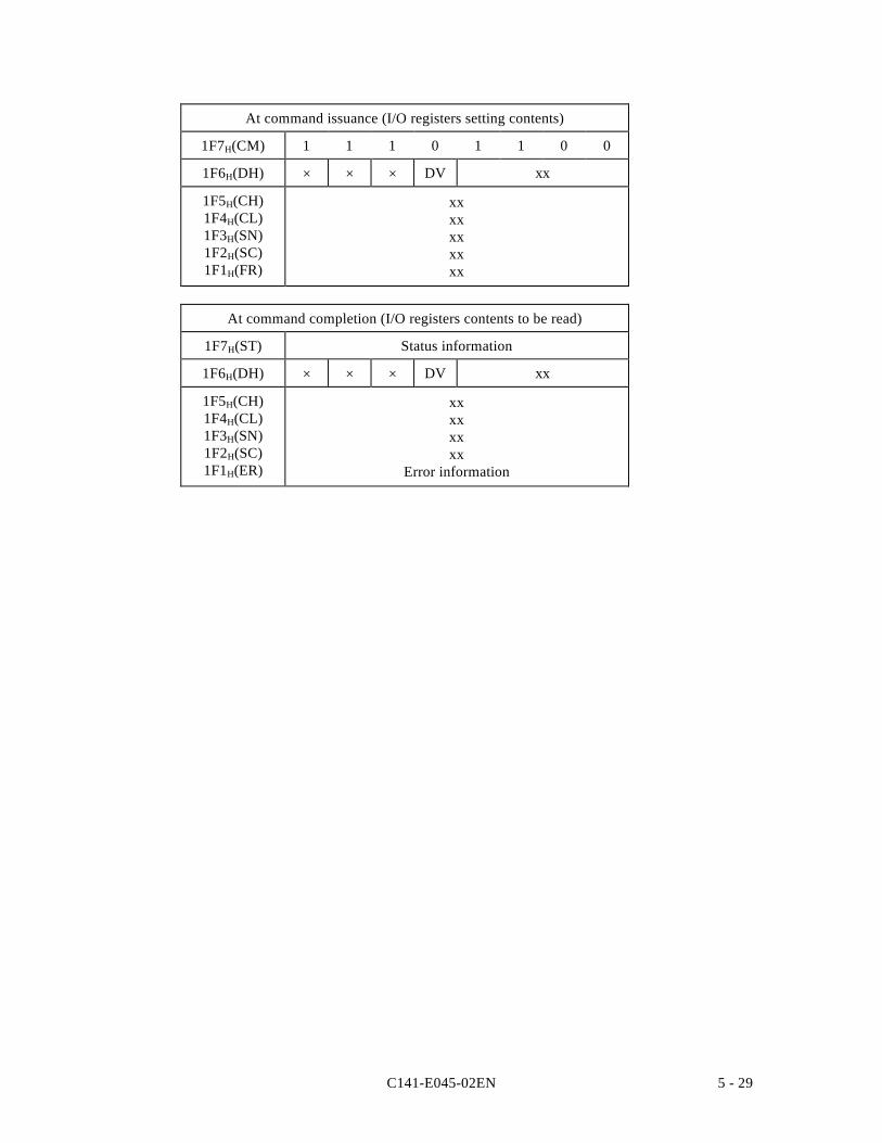
C141-E045-02EN 5 - 29
At command issuance (I/O registers setting contents)
1F7H(CM) 1 1 1 0 1 1 0 0
1F6H(DH) × × × DV xx
1F5H(CH)1F4H(CL)1F3H(SN)1F2H(SC)1F1H(FR)
xxxxxxxxxx
At command completion (I/O registers contents to be read)
1F7H(ST) Status information
1F6H(DH) × × × DV xx
1F5H(CH)1F4H(CL)1F3H(SN)1F2H(SC)1F1H(ER)
xxxxxxxx
Error information
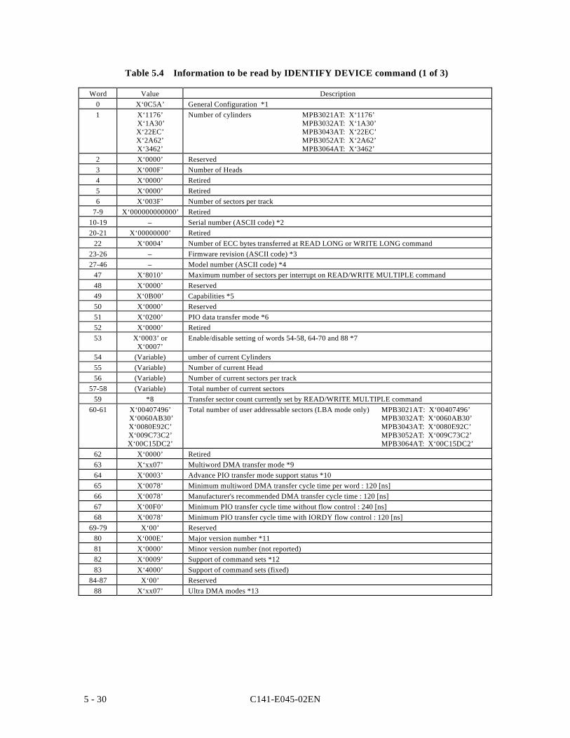
C141-E045-02EN5 - 30
Table 5.4 Information to be read by IDENTIFY DEVICE command (1 of 3)
Word Value Description0 X‘0C5A’ General Configuration *11 X‘1176’
X‘1A30’X‘22EC’X‘2A62’X‘3462’
Number of cylinders MPB3021AT: X‘1176’MPB3032AT: X‘1A30’MPB3043AT: X‘22EC’MPB3052AT: X‘2A62’MPB3064AT: X‘3462’
2 X‘0000’ Reserved3 X‘000F’ Number of Heads4 X‘0000’ Retired5 X‘0000’ Retired6 X‘003F’ Number of sectors per track
7-9 X‘000000000000’ Retired10-19 – Serial number (ASCII code) *220-21 X‘00000000’ Retired
22 X‘0004’ Number of ECC bytes transferred at READ LONG or WRITE LONG command23-26 – Firmware revision (ASCII code) *327-46 – Model number (ASCII code) *4
47 X‘8010’ Maximum number of sectors per interrupt on READ/WRITE MULTIPLE command48 X‘0000’ Reserved49 X‘0B00’ Capabilities *550 X‘0000’ Reserved51 X‘0200’ PIO data transfer mode *652 X‘0000’ Retired53 X‘0003’ or
X‘0007’Enable/disable setting of words 54-58, 64-70 and 88 *7
54 (Variable) umber of current Cylinders55 (Variable) Number of current Head56 (Variable) Number of current sectors per track
57-58 (Variable) Total number of current sectors59 *8 Transfer sector count currently set by READ/WRITE MULTIPLE command
60-61 X‘00407496’ X‘0060AB30’X‘0080E92C’X‘009C73C2’X‘00C15DC2’
Total number of user addressable sectors (LBA mode only) MPB3021AT: X‘00407496’MPB3032AT: X‘0060AB30’MPB3043AT: X‘0080E92C’MPB3052AT: X‘009C73C2’MPB3064AT: X‘00C15DC2’
62 X‘0000’ Retired63 X‘xx07’ Multiword DMA transfer mode *964 X‘0003’ Advance PIO transfer mode support status *1065 X‘0078’ Minimum multiword DMA transfer cycle time per word : 120 [ns]66 X‘0078’ Manufacturer's recommended DMA transfer cycle time : 120 [ns]67 X‘00F0’ Minimum PIO transfer cycle time without flow control : 240 [ns]68 X‘0078’ Minimum PIO transfer cycle time with IORDY flow control : 120 [ns]
69-79 X‘00’ Reserved80 X‘000E’ Major version number *1181 X‘0000’ Minor version number (not reported)82 X‘0009’ Support of command sets *1283 X‘4000’ Support of command sets (fixed)
84-87 X‘00’ Reserved88 X‘xx07’ Ultra DMA modes *13
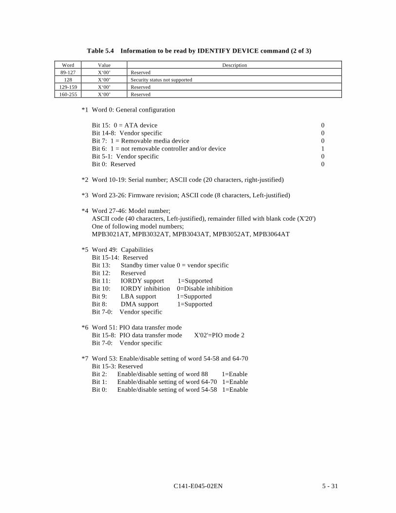
C141-E045-02EN 5 - 31
Table 5.4 Information to be read by IDENTIFY DEVICE command (2 of 3)
Word Value Description89-127 X‘00’ Reserved
128 X‘00’ Security status not supported129-159 X‘00’ Reserved160-255 X‘00’ Reserved
*1 Word 0: General configuration
Bit 15: 0 = ATA device 0Bit 14-8: Vendor specific 0Bit 7: 1 = Removable media device 0Bit 6: 1 = not removable controller and/or device 1Bit 5-1: Vendor specific 0Bit 0: Reserved 0
*2 Word 10-19: Serial number; ASCII code (20 characters, right-justified)
*3 Word 23-26: Firmware revision; ASCII code (8 characters, Left-justified)
*4 Word 27-46: Model number;ASCII code (40 characters, Left-justified), remainder filled with blank code (X'20')One of following model numbers;MPB3021AT, MPB3032AT, MPB3043AT, MPB3052AT, MPB3064AT
*5 Word 49: CapabilitiesBit 15-14: ReservedBit 13: Standby timer value 0 = vendor specificBit 12: ReservedBit 11: IORDY support 1=SupportedBit 10: IORDY inhibition 0=Disable inhibitionBit 9: LBA support 1=SupportedBit 8: DMA support 1=SupportedBit 7-0: Vendor specific
*6 Word 51: PIO data transfer modeBit 15-8: PIO data transfer mode X'02'=PIO mode 2Bit 7-0: Vendor specific
*7 Word 53: Enable/disable setting of word 54-58 and 64-70Bit 15-3: ReservedBit 2: Enable/disable setting of word 88 1=EnableBit 1: Enable/disable setting of word 64-70 1=EnableBit 0: Enable/disable setting of word 54-58 1=Enable
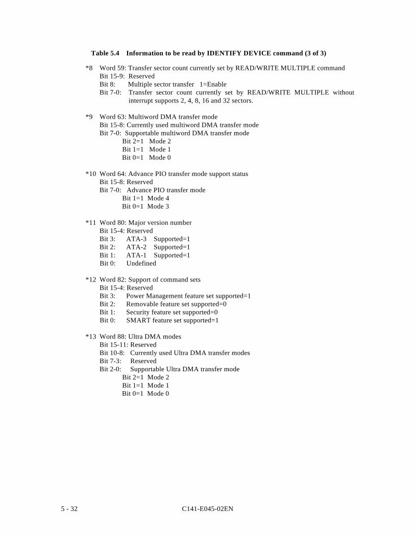
C141-E045-02EN5 - 32
Table 5.4 Information to be read by IDENTIFY DEVICE command (3 of 3)
*8 Word 59: Transfer sector count currently set by READ/WRITE MULTIPLE commandBit 15-9: ReservedBit 8: Multiple sector transfer 1=EnableBit 7-0: Transfer sector count currently set by READ/WRITE MULTIPLE without
interrupt supports 2, 4, 8, 16 and 32 sectors.
*9 Word 63: Multiword DMA transfer modeBit 15-8: Currently used multiword DMA transfer modeBit 7-0: Supportable multiword DMA transfer mode
Bit 2=1 Mode 2Bit 1=1 Mode 1Bit 0=1 Mode 0
*10 Word 64: Advance PIO transfer mode support statusBit 15-8: ReservedBit 7-0: Advance PIO transfer mode
Bit 1=1 Mode 4Bit 0=1 Mode 3
*11 Word 80: Major version numberBit 15-4: ReservedBit 3: ATA-3 Supported=1Bit 2: ATA-2 Supported=1Bit 1: ATA-1 Supported=1Bit 0: Undefined
*12 Word 82: Support of command setsBit 15-4: ReservedBit 3: Power Management feature set supported=1Bit 2: Removable feature set supported=0Bit 1: Security feature set supported=0Bit 0: SMART feature set supported=1
*13 Word 88: Ultra DMA modesBit 15-11: ReservedBit 10-8: Currently used Ultra DMA transfer modesBit 7-3: ReservedBit 2-0: Supportable Ultra DMA transfer mode
Bit 2=1 Mode 2Bit 1=1 Mode 1Bit 0=1 Mode 0
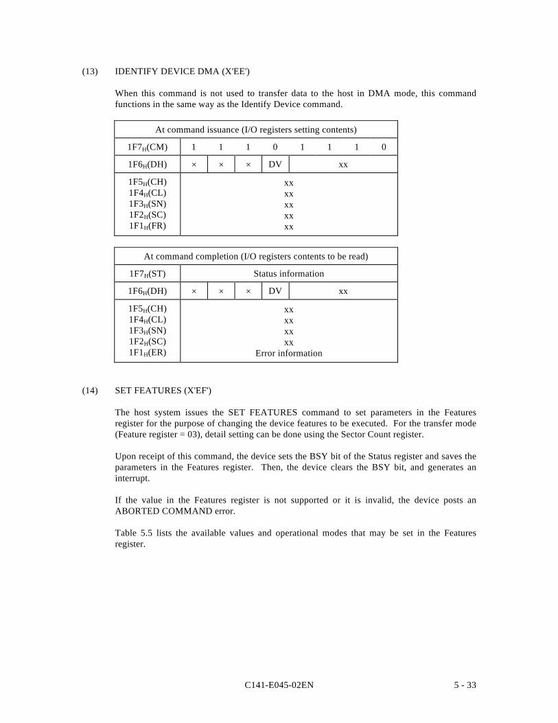
C141-E045-02EN 5 - 33
(13) IDENTIFY DEVICE DMA (X'EE')
When this command is not used to transfer data to the host in DMA mode, this commandfunctions in the same way as the Identify Device command.
At command issuance (I/O registers setting contents)
1F7H(CM) 1 1 1 0 1 1 1 0
1F6H(DH) × × × DV xx
1F5H(CH)1F4H(CL)1F3H(SN)1F2H(SC)1F1H(FR)
xxxxxxxxxx
At command completion (I/O registers contents to be read)
1F7H(ST) Status information
1F6H(DH) × × × DV xx
1F5H(CH)1F4H(CL)1F3H(SN)1F2H(SC)1F1H(ER)
xxxxxxxx
Error information
(14) SET FEATURES (X'EF')
The host system issues the SET FEATURES command to set parameters in the Featuresregister for the purpose of changing the device features to be executed. For the transfer mode(Feature register = 03), detail setting can be done using the Sector Count register.
Upon receipt of this command, the device sets the BSY bit of the Status register and saves theparameters in the Features register. Then, the device clears the BSY bit, and generates aninterrupt.
If the value in the Features register is not supported or it is invalid, the device posts anABORTED COMMAND error.
Table 5.5 lists the available values and operational modes that may be set in the Featuresregister.
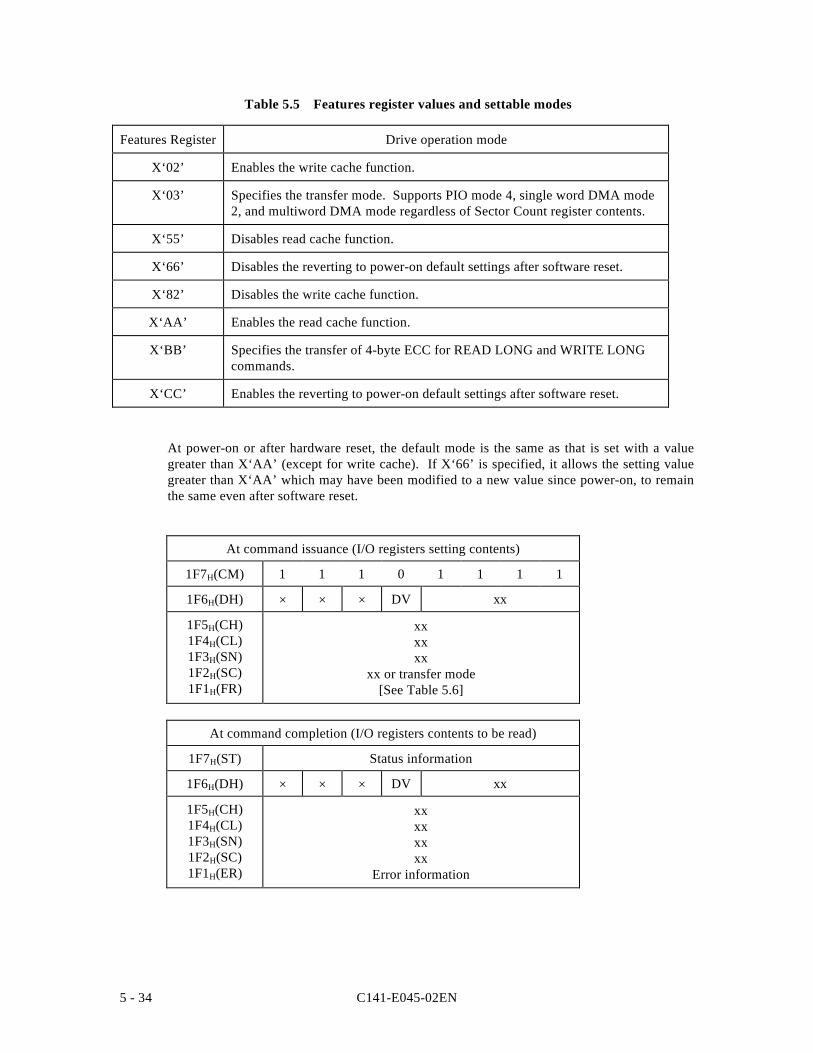
C141-E045-02EN5 - 34
Table 5.5 Features register values and settable modes
Features Register Drive operation mode
X‘02’ Enables the write cache function.
X‘03’ Specifies the transfer mode. Supports PIO mode 4, single word DMA mode2, and multiword DMA mode regardless of Sector Count register contents.
X‘55’ Disables read cache function.
X‘66’ Disables the reverting to power-on default settings after software reset.
X‘82’ Disables the write cache function.
X‘AA’ Enables the read cache function.
X‘BB’ Specifies the transfer of 4-byte ECC for READ LONG and WRITE LONGcommands.
X‘CC’ Enables the reverting to power-on default settings after software reset.
At power-on or after hardware reset, the default mode is the same as that is set with a valuegreater than X‘AA’ (except for write cache). If X‘66’ is specified, it allows the setting valuegreater than X‘AA’ which may have been modified to a new value since power-on, to remainthe same even after software reset.
At command issuance (I/O registers setting contents)
1F7H(CM) 1 1 1 0 1 1 1 1
1F6H(DH) × × × DV xx
1F5H(CH)1F4H(CL)1F3H(SN)1F2H(SC)1F1H(FR)
xxxxxx
xx or transfer mode[See Table 5.6]
At command completion (I/O registers contents to be read)
1F7H(ST) Status information
1F6H(DH) × × × DV xx
1F5H(CH)1F4H(CL)1F3H(SN)1F2H(SC)1F1H(ER)
xxxxxxxx
Error information
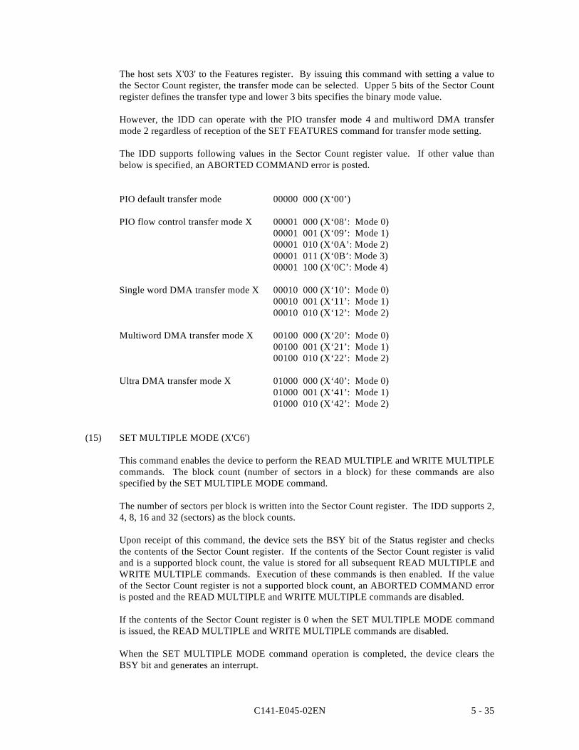
C141-E045-02EN 5 - 35
The host sets X'03' to the Features register. By issuing this command with setting a value tothe Sector Count register, the transfer mode can be selected. Upper 5 bits of the Sector Countregister defines the transfer type and lower 3 bits specifies the binary mode value.
However, the IDD can operate with the PIO transfer mode 4 and multiword DMA transfermode 2 regardless of reception of the SET FEATURES command for transfer mode setting.
The IDD supports following values in the Sector Count register value. If other value thanbelow is specified, an ABORTED COMMAND error is posted.
PIO default transfer mode 00000 000 (X‘00’)
PIO flow control transfer mode X 00001 000 (X‘08’: Mode 0)00001 001 (X‘09’: Mode 1)00001 010 (X‘0A’: Mode 2)00001 011 (X‘0B’: Mode 3)00001 100 (X‘0C’: Mode 4)
Single word DMA transfer mode X 00010 000 (X‘10’: Mode 0)00010 001 (X‘11’: Mode 1)00010 010 (X‘12’: Mode 2)
Multiword DMA transfer mode X 00100 000 (X‘20’: Mode 0)00100 001 (X‘21’: Mode 1)00100 010 (X‘22’: Mode 2)
Ultra DMA transfer mode X 01000 000 (X‘40’: Mode 0)01000 001 (X‘41’: Mode 1)01000 010 (X‘42’: Mode 2)
(15) SET MULTIPLE MODE (X'C6')
This command enables the device to perform the READ MULTIPLE and WRITE MULTIPLEcommands. The block count (number of sectors in a block) for these commands are alsospecified by the SET MULTIPLE MODE command.
The number of sectors per block is written into the Sector Count register. The IDD supports 2,4, 8, 16 and 32 (sectors) as the block counts.
Upon receipt of this command, the device sets the BSY bit of the Status register and checksthe contents of the Sector Count register. If the contents of the Sector Count register is validand is a supported block count, the value is stored for all subsequent READ MULTIPLE andWRITE MULTIPLE commands. Execution of these commands is then enabled. If the valueof the Sector Count register is not a supported block count, an ABORTED COMMAND erroris posted and the READ MULTIPLE and WRITE MULTIPLE commands are disabled.
If the contents of the Sector Count register is 0 when the SET MULTIPLE MODE commandis issued, the READ MULTIPLE and WRITE MULTIPLE commands are disabled.
When the SET MULTIPLE MODE command operation is completed, the device clears theBSY bit and generates an interrupt.
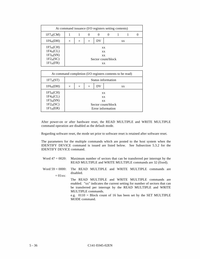
C141-E045-02EN5 - 36
At command issuance (I/O registers setting contents)
1F7H(CM) 1 1 0 0 0 1 1 0
1F6H(DH) × × × DV xx
1F5H(CH)1F4H(CL)1F3H(SN)1F2H(SC)1F1H(FR)
xxxxxx
Sector count/blockxx
At command completion (I/O registers contents to be read)
1F7H(ST) Status information
1F6H(DH) × × × DV xx
1F5H(CH)1F4H(CL)1F3H(SN)1F2H(SC)1F1H(ER)
xxxxxx
Sector count/blockError information
After power-on or after hardware reset, the READ MULTIPLE and WRITE MULTIPLEcommand operation are disabled as the default mode.
Regarding software reset, the mode set prior to software reset is retained after software reset.
The parameters for the multiple commands which are posted to the host system when theIDENTIFY DEVICE command is issued are listed below. See Subsection 5.3.2 for theIDENTIFY DEVICE command.
Word 47 = 0020:
Word 59 = 0000:
= 01xx:
Maximum number of sectors that can be transferred per interrupt by theREAD MULTIPLE and WRITE MULTIPLE commands are 32 (fixed).
The READ MULTIPLE and WRITE MULTIPLE commands aredisabled.
The READ MULTIPLE and WRITE MULTIPLE commands areenabled. "xx" indicates the current setting for number of sectors that canbe transferred per interrupt by the READ MULTIPLE and WRITEMULTIPLE commands.e.g. 0110 = Block count of 16 has been set by the SET MULTIPLEMODE command.
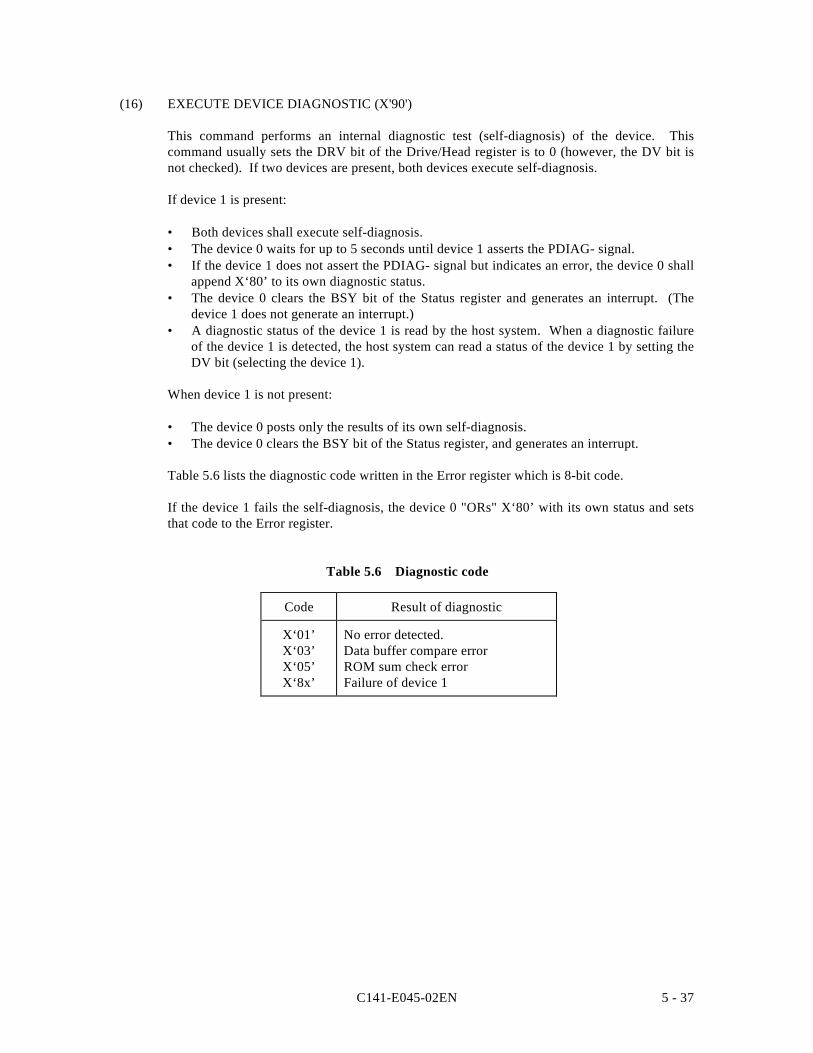
C141-E045-02EN 5 - 37
(16) EXECUTE DEVICE DIAGNOSTIC (X'90')
This command performs an internal diagnostic test (self-diagnosis) of the device. Thiscommand usually sets the DRV bit of the Drive/Head register is to 0 (however, the DV bit isnot checked). If two devices are present, both devices execute self-diagnosis.
If device 1 is present:
• Both devices shall execute self-diagnosis.• The device 0 waits for up to 5 seconds until device 1 asserts the PDIAG- signal.• If the device 1 does not assert the PDIAG- signal but indicates an error, the device 0 shall
append X‘80’ to its own diagnostic status.• The device 0 clears the BSY bit of the Status register and generates an interrupt. (The
device 1 does not generate an interrupt.)• A diagnostic status of the device 1 is read by the host system. When a diagnostic failure
of the device 1 is detected, the host system can read a status of the device 1 by setting theDV bit (selecting the device 1).
When device 1 is not present:
• The device 0 posts only the results of its own self-diagnosis.• The device 0 clears the BSY bit of the Status register, and generates an interrupt.
Table 5.6 lists the diagnostic code written in the Error register which is 8-bit code.
If the device 1 fails the self-diagnosis, the device 0 "ORs" X‘80’ with its own status and setsthat code to the Error register.
Table 5.6 Diagnostic code
Code Result of diagnostic
X‘01’X‘03’X‘05’X‘8x’
No error detected.Data buffer compare errorROM sum check errorFailure of device 1
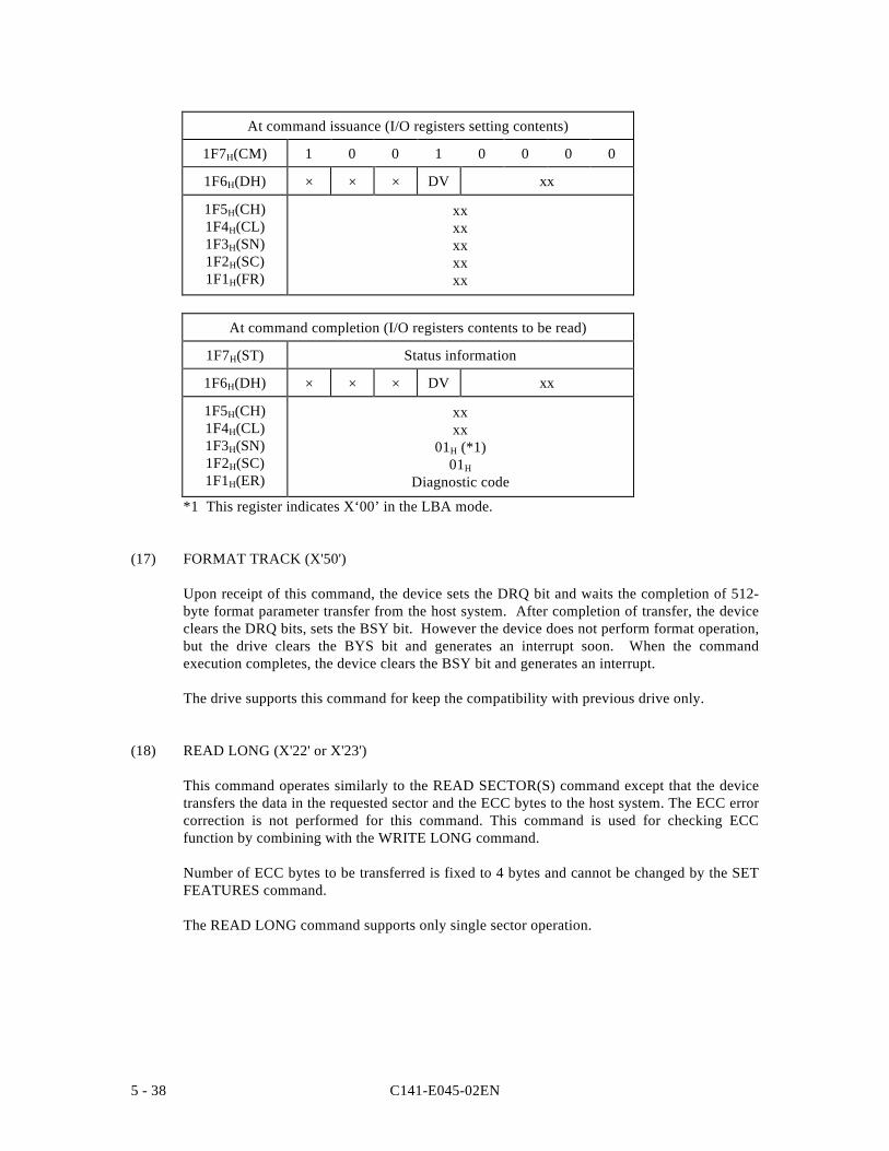
C141-E045-02EN5 - 38
At command issuance (I/O registers setting contents)
1F7H(CM) 1 0 0 1 0 0 0 0
1F6H(DH) × × × DV xx
1F5H(CH)1F4H(CL)1F3H(SN)1F2H(SC)1F1H(FR)
xxxxxxxxxx
At command completion (I/O registers contents to be read)
1F7H(ST) Status information
1F6H(DH) × × × DV xx
1F5H(CH)1F4H(CL)1F3H(SN)1F2H(SC)1F1H(ER)
xxxx
01H (*1)01H
Diagnostic code
*1 This register indicates X‘00’ in the LBA mode.
(17) FORMAT TRACK (X'50')
Upon receipt of this command, the device sets the DRQ bit and waits the completion of 512-byte format parameter transfer from the host system. After completion of transfer, the deviceclears the DRQ bits, sets the BSY bit. However the device does not perform format operation,but the drive clears the BYS bit and generates an interrupt soon. When the commandexecution completes, the device clears the BSY bit and generates an interrupt.
The drive supports this command for keep the compatibility with previous drive only.
(18) READ LONG (X'22' or X'23')
This command operates similarly to the READ SECTOR(S) command except that the devicetransfers the data in the requested sector and the ECC bytes to the host system. The ECC errorcorrection is not performed for this command. This command is used for checking ECCfunction by combining with the WRITE LONG command.
Number of ECC bytes to be transferred is fixed to 4 bytes and cannot be changed by the SETFEATURES command.
The READ LONG command supports only single sector operation.
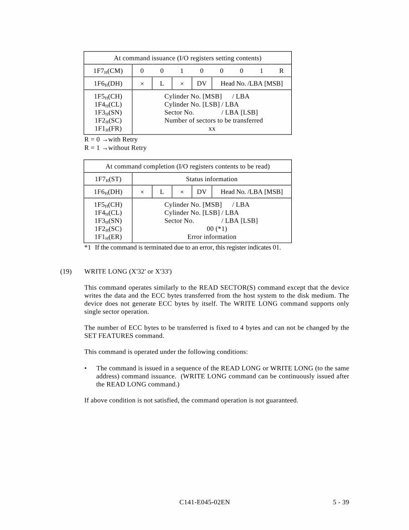
C141-E045-02EN 5 - 39
At command issuance (I/O registers setting contents)
1F7H(CM) 0 0 1 0 0 0 1 R
1F6H(DH) × L × DV Head No. /LBA [MSB]
1F5H(CH)1F4H(CL)1F3H(SN)1F2H(SC)1F1H(FR)
Cylinder No. [MSB] / LBACylinder No. [LSB] / LBASector No. / LBA [LSB]Number of sectors to be transferred xx
R = 0 →with RetryR = 1 →without Retry
At command completion (I/O registers contents to be read)
1F7H(ST) Status information
1F6H(DH) × L × DV Head No. /LBA [MSB]
1F5H(CH)1F4H(CL)1F3H(SN)1F2H(SC)1F1H(ER)
Cylinder No. [MSB] / LBACylinder No. [LSB] / LBASector No. / LBA [LSB] 00 (*1) Error information
*1 If the command is terminated due to an error, this register indicates 01.
(19) WRITE LONG (X'32' or X'33')
This command operates similarly to the READ SECTOR(S) command except that the devicewrites the data and the ECC bytes transferred from the host system to the disk medium. Thedevice does not generate ECC bytes by itself. The WRITE LONG command supports onlysingle sector operation.
The number of ECC bytes to be transferred is fixed to 4 bytes and can not be changed by theSET FEATURES command.
This command is operated under the following conditions:
• The command is issued in a sequence of the READ LONG or WRITE LONG (to the sameaddress) command issuance. (WRITE LONG command can be continuously issued afterthe READ LONG command.)
If above condition is not satisfied, the command operation is not guaranteed.
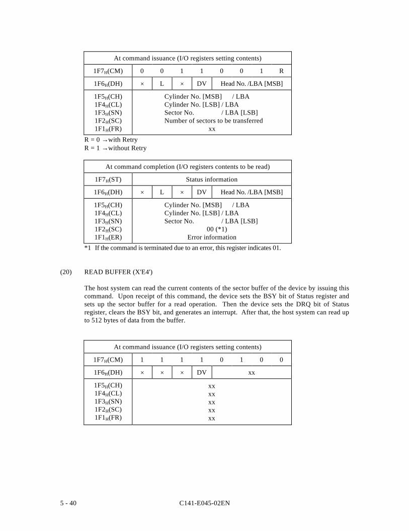
C141-E045-02EN5 - 40
At command issuance (I/O registers setting contents)
1F7H(CM) 0 0 1 1 0 0 1 R
1F6H(DH) × L × DV Head No. /LBA [MSB]
1F5H(CH)1F4H(CL)1F3H(SN)1F2H(SC)1F1H(FR)
Cylinder No. [MSB] / LBACylinder No. [LSB] / LBASector No. / LBA [LSB]Number of sectors to be transferred xx
R = 0 →with RetryR = 1 →without Retry
At command completion (I/O registers contents to be read)
1F7H(ST) Status information
1F6H(DH) × L × DV Head No. /LBA [MSB]
1F5H(CH)1F4H(CL)1F3H(SN)1F2H(SC)1F1H(ER)
Cylinder No. [MSB] / LBACylinder No. [LSB] / LBASector No. / LBA [LSB] 00 (*1) Error information
*1 If the command is terminated due to an error, this register indicates 01.
(20) READ BUFFER (X'E4')
The host system can read the current contents of the sector buffer of the device by issuing thiscommand. Upon receipt of this command, the device sets the BSY bit of Status register andsets up the sector buffer for a read operation. Then the device sets the DRQ bit of Statusregister, clears the BSY bit, and generates an interrupt. After that, the host system can read upto 512 bytes of data from the buffer.
At command issuance (I/O registers setting contents)
1F7H(CM) 1 1 1 1 0 1 0 0
1F6H(DH) × × × DV xx
1F5H(CH)1F4H(CL)1F3H(SN)1F2H(SC)1F1H(FR)
xxxxxxxxxx
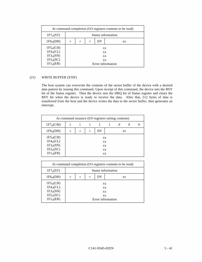
C141-E045-02EN 5 - 41
At command completion (I/O registers contents to be read)
1F7H(ST) Status information
1F6H(DH) × × × DV xx
1F5H(CH)1F4H(CL)1F3H(SN)1F2H(SC)1F1H(ER)
xxxxxxxx
Error information
(21) WRITE BUFFER (X'E8')
The host system can overwrite the contents of the sector buffer of the device with a desireddata pattern by issuing this command. Upon receipt of this command, the device sets the BSYbit of the Status register. Then the device sets the DRQ bit of Status register and clears theBSY bit when the device is ready to receive the data. After that, 512 bytes of data istransferred from the host and the device writes the data to the sector buffer, then generates aninterrupt.
At command issuance (I/O registers setting contents)
1F7H(CM) 1 1 1 1 1 0 0 0
1F6H(DH) × × × DV xx
1F5H(CH)1F4H(CL)1F3H(SN)1F2H(SC)1F1H(FR)
xxxxxxxxxx
At command completion (I/O registers contents to be read)
1F7H(ST) Status information
1F6H(DH) × × × DV xx
1F5H(CH)1F4H(CL)1F3H(SN)1F2H(SC)1F1H(ER)
xxxxxxxx
Error information
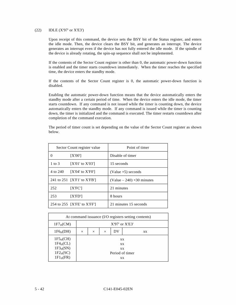
C141-E045-02EN5 - 42
(22) IDLE (X'97' or X'E3')
Upon receipt of this command, the device sets the BSY bit of the Status register, and entersthe idle mode. Then, the device clears the BSY bit, and generates an interrupt. The devicegenerates an interrupt even if the device has not fully entered the idle mode. If the spindle ofthe device is already rotating, the spin-up sequence shall not be implemented.
If the contents of the Sector Count register is other than 0, the automatic power-down functionis enabled and the timer starts countdown immediately. When the timer reaches the specifiedtime, the device enters the standby mode.
If the contents of the Sector Count register is 0, the automatic power-down function isdisabled.
Enabling the automatic power-down function means that the device automatically enters thestandby mode after a certain period of time. When the device enters the idle mode, the timerstarts countdown. If any command is not issued while the timer is counting down, the deviceautomatically enters the standby mode. If any command is issued while the timer is countingdown, the timer is initialized and the command is executed. The timer restarts countdown aftercompletion of the command execution.
The period of timer count is set depending on the value of the Sector Count register as shownbelow.
Sector Count register value Point of timer
0 [X'00'] Disable of timer
1 to 3 [X'01' to X'03'] 15 seconds
4 to 240 [X'04' to X'F0'] (Value ×5) seconds
241 to 251 [X'F1' to X'FB'] (Value – 240) ×30 minutes
252 [X'FC'] 21 minutes
253 [X'FD'] 8 hours
254 to 255 [X'FE' to X'FF'] 21 minutes 15 seconds
At command issuance (I/O registers setting contents)
1F7H(CM) X'97' or X'E3'
1F6H(DH) × × × DV xx
1F5H(CH)1F4H(CL)1F3H(SN)1F2H(SC)1F1H(FR)
xxxxxx
Period of timerxx
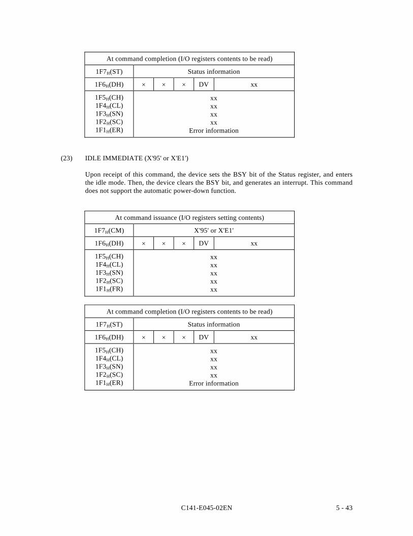
C141-E045-02EN 5 - 43
At command completion (I/O registers contents to be read)
1F7H(ST) Status information
1F6H(DH) × × × DV xx
1F5H(CH)1F4H(CL)1F3H(SN)1F2H(SC)1F1H(ER)
xxxxxxxx
Error information
(23) IDLE IMMEDIATE (X'95' or X'E1')
Upon receipt of this command, the device sets the BSY bit of the Status register, and entersthe idle mode. Then, the device clears the BSY bit, and generates an interrupt. This commanddoes not support the automatic power-down function.
At command issuance (I/O registers setting contents)
1F7H(CM) X'95' or X'E1'
1F6H(DH) × × × DV xx
1F5H(CH)1F4H(CL)1F3H(SN)1F2H(SC)1F1H(FR)
xxxxxxxxxx
At command completion (I/O registers contents to be read)
1F7H(ST) Status information
1F6H(DH) × × × DV xx
1F5H(CH)1F4H(CL)1F3H(SN)1F2H(SC)1F1H(ER)
xxxxxxxx
Error information
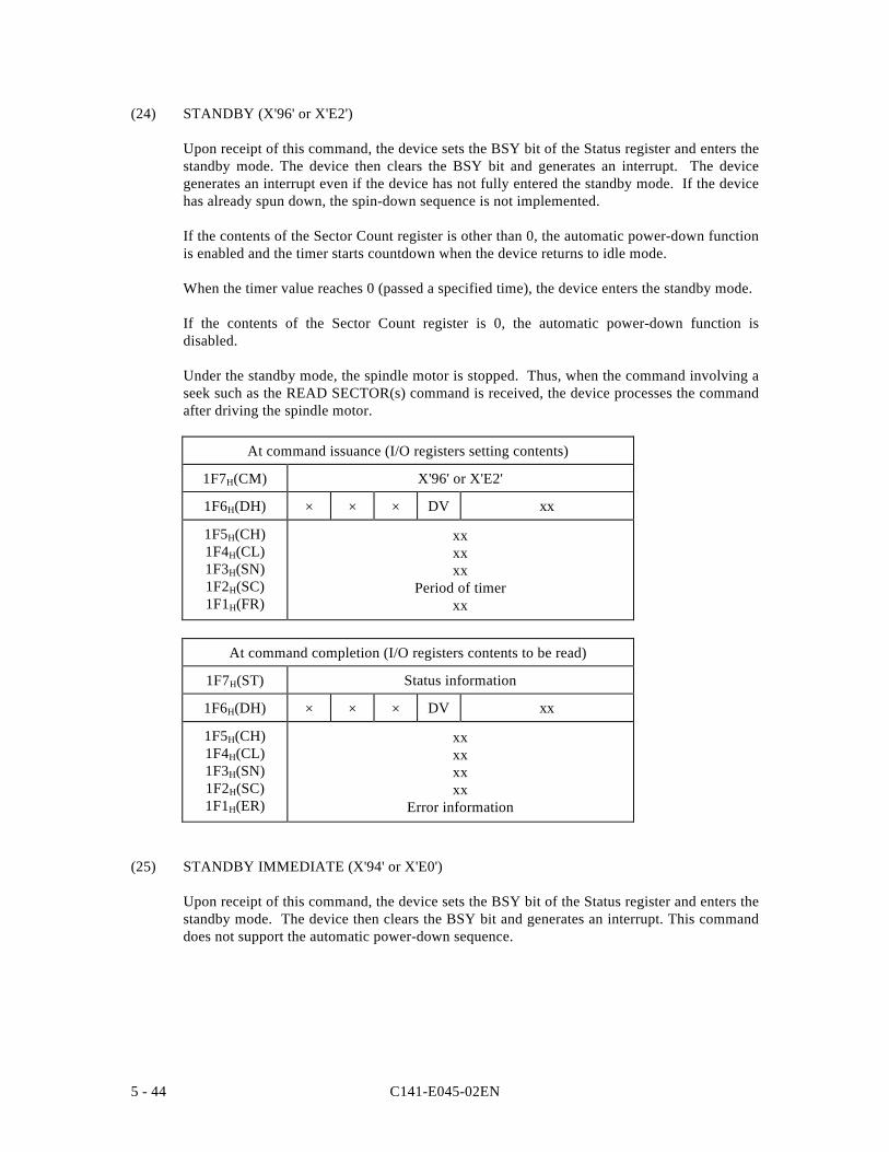
C141-E045-02EN5 - 44
(24) STANDBY (X'96' or X'E2')
Upon receipt of this command, the device sets the BSY bit of the Status register and enters thestandby mode. The device then clears the BSY bit and generates an interrupt. The devicegenerates an interrupt even if the device has not fully entered the standby mode. If the devicehas already spun down, the spin-down sequence is not implemented.
If the contents of the Sector Count register is other than 0, the automatic power-down functionis enabled and the timer starts countdown when the device returns to idle mode.
When the timer value reaches 0 (passed a specified time), the device enters the standby mode.
If the contents of the Sector Count register is 0, the automatic power-down function isdisabled.
Under the standby mode, the spindle motor is stopped. Thus, when the command involving aseek such as the READ SECTOR(s) command is received, the device processes the commandafter driving the spindle motor.
At command issuance (I/O registers setting contents)
1F7H(CM) X'96' or X'E2'
1F6H(DH) × × × DV xx
1F5H(CH)1F4H(CL)1F3H(SN)1F2H(SC)1F1H(FR)
xxxxxx
Period of timerxx
At command completion (I/O registers contents to be read)
1F7H(ST) Status information
1F6H(DH) × × × DV xx
1F5H(CH)1F4H(CL)1F3H(SN)1F2H(SC)1F1H(ER)
xxxxxxxx
Error information
(25) STANDBY IMMEDIATE (X'94' or X'E0')
Upon receipt of this command, the device sets the BSY bit of the Status register and enters thestandby mode. The device then clears the BSY bit and generates an interrupt. This commanddoes not support the automatic power-down sequence.
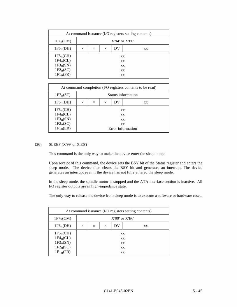
C141-E045-02EN 5 - 45
At command issuance (I/O registers setting contents)
1F7H(CM) X'94' or X'E0'
1F6H(DH) × × × DV xx
1F5H(CH)1F4H(CL)1F3H(SN)1F2H(SC)1F1H(FR)
xxxxxxxxxx
At command completion (I/O registers contents to be read)
1F7H(ST) Status information
1F6H(DH) × × × DV xx
1F5H(CH)1F4H(CL)1F3H(SN)1F2H(SC)1F1H(ER)
xxxxxxxx
Error information
(26) SLEEP (X'99' or X'E6')
This command is the only way to make the device enter the sleep mode.
Upon receipt of this command, the device sets the BSY bit of the Status register and enters thesleep mode. The device then clears the BSY bit and generates an interrupt. The devicegenerates an interrupt even if the device has not fully entered the sleep mode.
In the sleep mode, the spindle motor is stopped and the ATA interface section is inactive. AllI/O register outputs are in high-impedance state.
The only way to release the device from sleep mode is to execute a software or hardware reset.
At command issuance (I/O registers setting contents)
1F7H(CM) X'99' or X'E6'
1F6H(DH) × × × DV xx
1F5H(CH)1F4H(CL)1F3H(SN)1F2H(SC)1F1H(FR)
xxxxxxxxxx
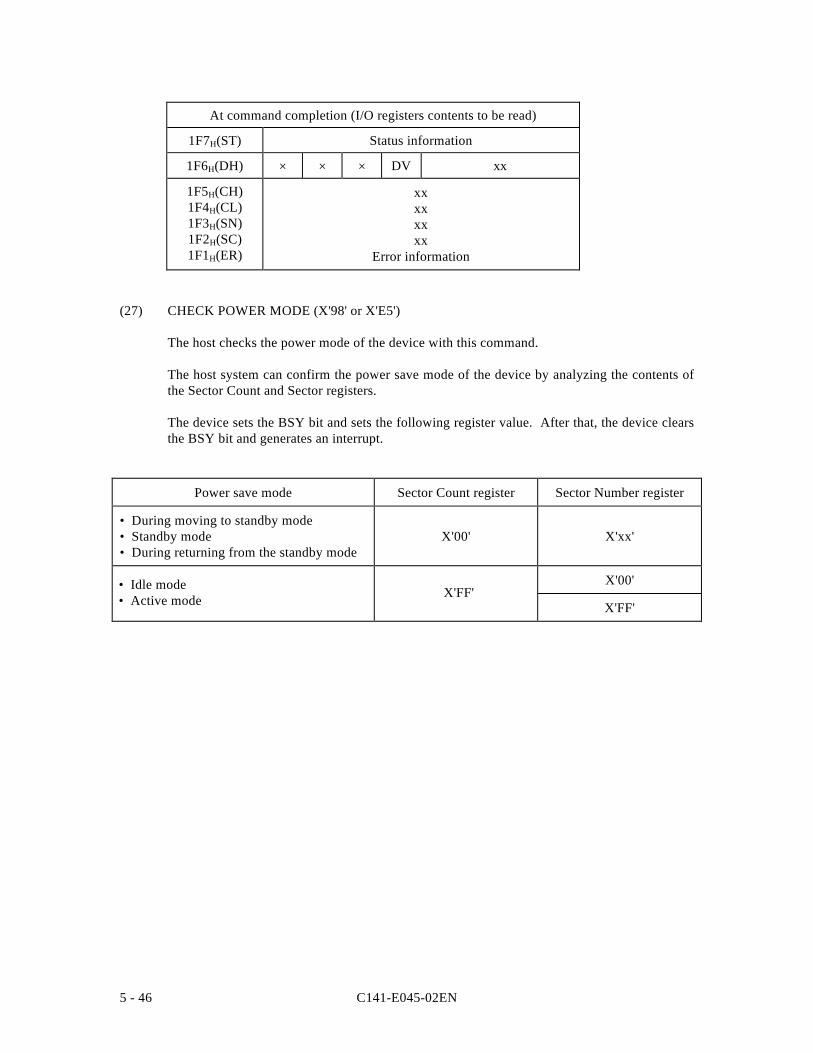
C141-E045-02EN5 - 46
At command completion (I/O registers contents to be read)
1F7H(ST) Status information
1F6H(DH) × × × DV xx
1F5H(CH)1F4H(CL)1F3H(SN)1F2H(SC)1F1H(ER)
xxxxxxxx
Error information
(27) CHECK POWER MODE (X'98' or X'E5')
The host checks the power mode of the device with this command.
The host system can confirm the power save mode of the device by analyzing the contents ofthe Sector Count and Sector registers.
The device sets the BSY bit and sets the following register value. After that, the device clearsthe BSY bit and generates an interrupt.
Power save mode Sector Count register Sector Number register
• During moving to standby mode• Standby mode• During returning from the standby mode
X'00' X'xx'
X'00'
X'FF'X'FF'• Idle mode
• Active mode
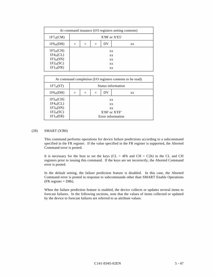
C141-E045-02EN 5 - 47
At command issuance (I/O registers setting contents)
1F7H(CM) X'98' or X'E5'
1F6H(DH) × × × DV xx
1F5H(CH)1F4H(CL)1F3H(SN)1F2H(SC)1F1H(FR)
xxxxxxxxxx
At command completion (I/O registers contents to be read)
1F7H(ST) Status information
1F6H(DH) × × × DV xx
1F5H(CH)1F4H(CL)1F3H(SN)1F2H(SC)1F1H(ER)
xxxxxx
X'00' or X'FF'Error information
(28) SMART (X'B0)
This command performs operations for device failure predictions according to a subcommandspecified in the FR register. If the value specified in the FR register is supported, the AbortedCommand error is posted.
It is necessary for the host to set the keys (CL = 4Fh and CH = C2h) in the CL and CHregisters prior to issuing this command. If the keys are set incorrectly, the Aborted Commanderror is posted.
In the default setting, the failure prediction feature is disabled. In this case, the AbortedCommand error is posted in response to subcommands other than SMART Enable Operations(FR register = D8h).
When the failure prediction feature is enabled, the device collects or updates several items toforecast failures. In the following sections, note that the values of items collected or updatedby the device to forecast failures are referred to as attribute values.
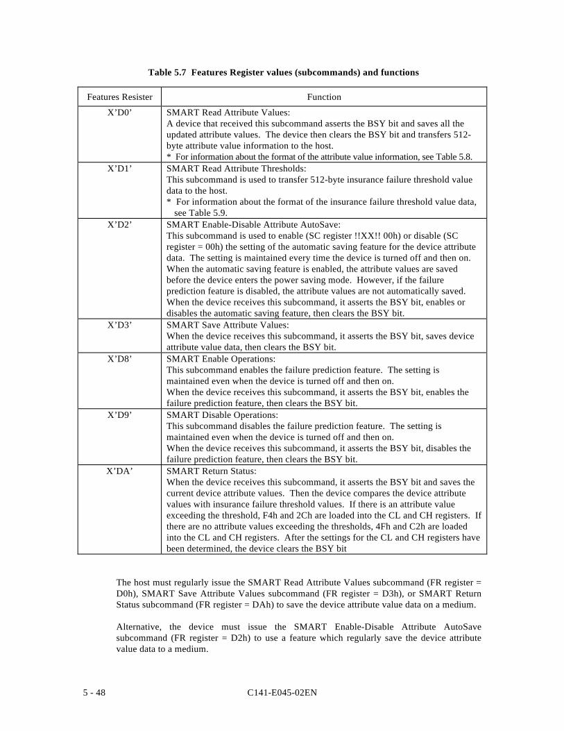
C141-E045-02EN5 - 48
Table 5.7 Features Register values (subcommands) and functions
Features Resister Function
X’D0’ SMART Read Attribute Values:A device that received this subcommand asserts the BSY bit and saves all theupdated attribute values. The device then clears the BSY bit and transfers 512-byte attribute value information to the host.* For information about the format of the attribute value information, see Table 5.8.
X’D1’ SMART Read Attribute Thresholds:This subcommand is used to transfer 512-byte insurance failure threshold valuedata to the host.* For information about the format of the insurance failure threshold value data,
see Table 5.9.X’D2’ SMART Enable-Disable Attribute AutoSave:
This subcommand is used to enable (SC register !!XX!! 00h) or disable (SCregister = 00h) the setting of the automatic saving feature for the device attributedata. The setting is maintained every time the device is turned off and then on.When the automatic saving feature is enabled, the attribute values are savedbefore the device enters the power saving mode. However, if the failureprediction feature is disabled, the attribute values are not automatically saved.When the device receives this subcommand, it asserts the BSY bit, enables ordisables the automatic saving feature, then clears the BSY bit.
X’D3’ SMART Save Attribute Values:When the device receives this subcommand, it asserts the BSY bit, saves deviceattribute value data, then clears the BSY bit.
X’D8’ SMART Enable Operations:This subcommand enables the failure prediction feature. The setting ismaintained even when the device is turned off and then on.When the device receives this subcommand, it asserts the BSY bit, enables thefailure prediction feature, then clears the BSY bit.
X’D9’ SMART Disable Operations:This subcommand disables the failure prediction feature. The setting ismaintained even when the device is turned off and then on.When the device receives this subcommand, it asserts the BSY bit, disables thefailure prediction feature, then clears the BSY bit.
X’DA’ SMART Return Status:When the device receives this subcommand, it asserts the BSY bit and saves thecurrent device attribute values. Then the device compares the device attributevalues with insurance failure threshold values. If there is an attribute valueexceeding the threshold, F4h and 2Ch are loaded into the CL and CH registers. Ifthere are no attribute values exceeding the thresholds, 4Fh and C2h are loadedinto the CL and CH registers. After the settings for the CL and CH registers havebeen determined, the device clears the BSY bit
The host must regularly issue the SMART Read Attribute Values subcommand (FR register =D0h), SMART Save Attribute Values subcommand (FR register = D3h), or SMART ReturnStatus subcommand (FR register = DAh) to save the device attribute value data on a medium.
Alternative, the device must issue the SMART Enable-Disable Attribute AutoSavesubcommand (FR register = D2h) to use a feature which regularly save the device attributevalue data to a medium.
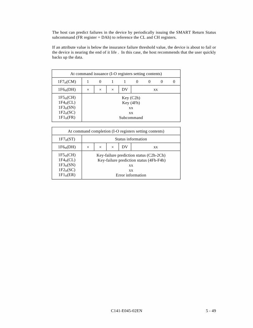
C141-E045-02EN 5 - 49
The host can predict failures in the device by periodically issuing the SMART Return Statussubcommand (FR register = DAh) to reference the CL and CH registers.
If an attribute value is below the insurance failure threshold value, the device is about to fail orthe device is nearing the end of it life . In this case, the host recommends that the user quicklybacks up the data.
At command issuance (I-O registers setting contents)
1F7H(CM) 1 0 1 1 0 0 0 0
1F6H(DH) × × × DV xx
1F5H(CH)1F4H(CL)1F3H(SN)1F2H(SC)1F1H(FR)
Key (C2h)Key (4Fh)
xxxx
Subcommand
At command completion (I-O registers setting contents)
1F7H(ST) Status information
1F6H(DH) × × × DV xx
1F5H(CH)1F4H(CL)1F3H(SN)1F2H(SC)1F1H(ER)
Key-failure prediction status (C2h-2Ch) Key-failure prediction status (4Fh-F4h)
xxxx
Error information
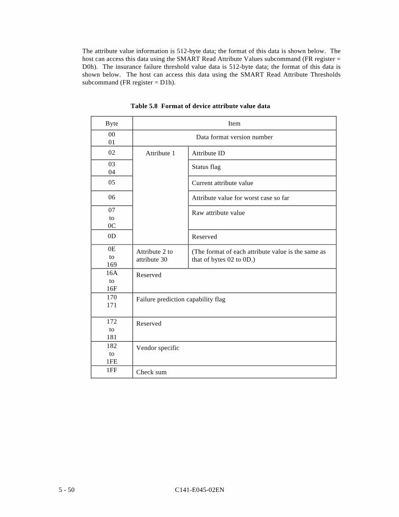
C141-E045-02EN5 - 50
The attribute value information is 512-byte data; the format of this data is shown below. Thehost can access this data using the SMART Read Attribute Values subcommand (FR register =D0h). The insurance failure threshold value data is 512-byte data; the format of this data isshown below. The host can access this data using the SMART Read Attribute Thresholdssubcommand (FR register = D1h).
Table 5.8 Format of device attribute value data
Byte Item
0001
Data format version number
02 Attribute 1 Attribute ID
0304
Status flag
05 Current attribute value
06 Attribute value for worst case so far
07to0C
Raw attribute value
0D Reserved
0Eto
169
Attribute 2 toattribute 30
(The format of each attribute value is the same asthat of bytes 02 to 0D.)
16Ato
16F
Reserved
170171
Failure prediction capability flag
172to
181
Reserved
182to
1FE
Vendor specific
1FF Check sum
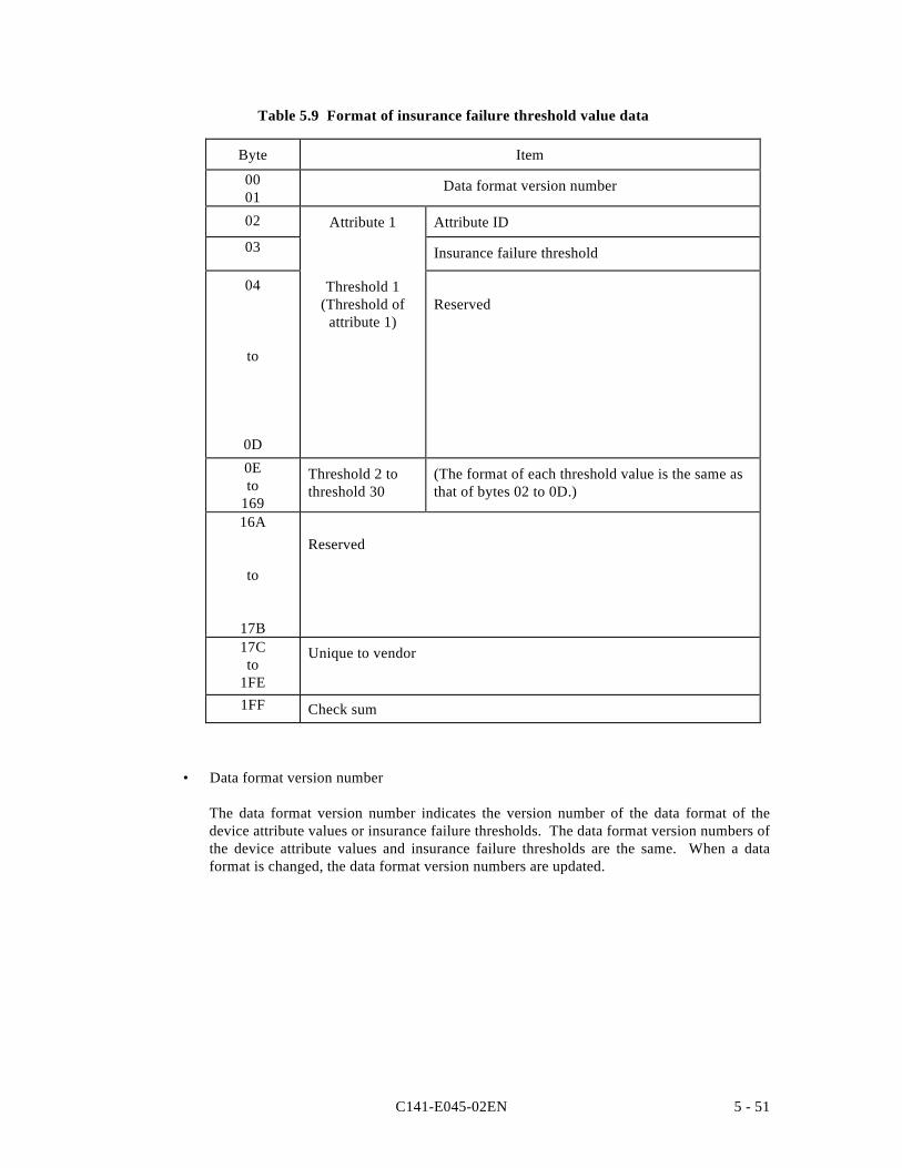
C141-E045-02EN 5 - 51
Table 5.9 Format of insurance failure threshold value data
Byte Item
0001
Data format version number
02 Attribute 1 Attribute ID
03 Insurance failure threshold
04
to
0D
Threshold 1(Threshold of
attribute 1)Reserved
0Eto
169
Threshold 2 tothreshold 30
(The format of each threshold value is the same asthat of bytes 02 to 0D.)
16A
to
17B
Reserved
17Cto
1FE
Unique to vendor
1FF Check sum
• Data format version number
The data format version number indicates the version number of the data format of thedevice attribute values or insurance failure thresholds. The data format version numbers ofthe device attribute values and insurance failure thresholds are the same. When a dataformat is changed, the data format version numbers are updated.
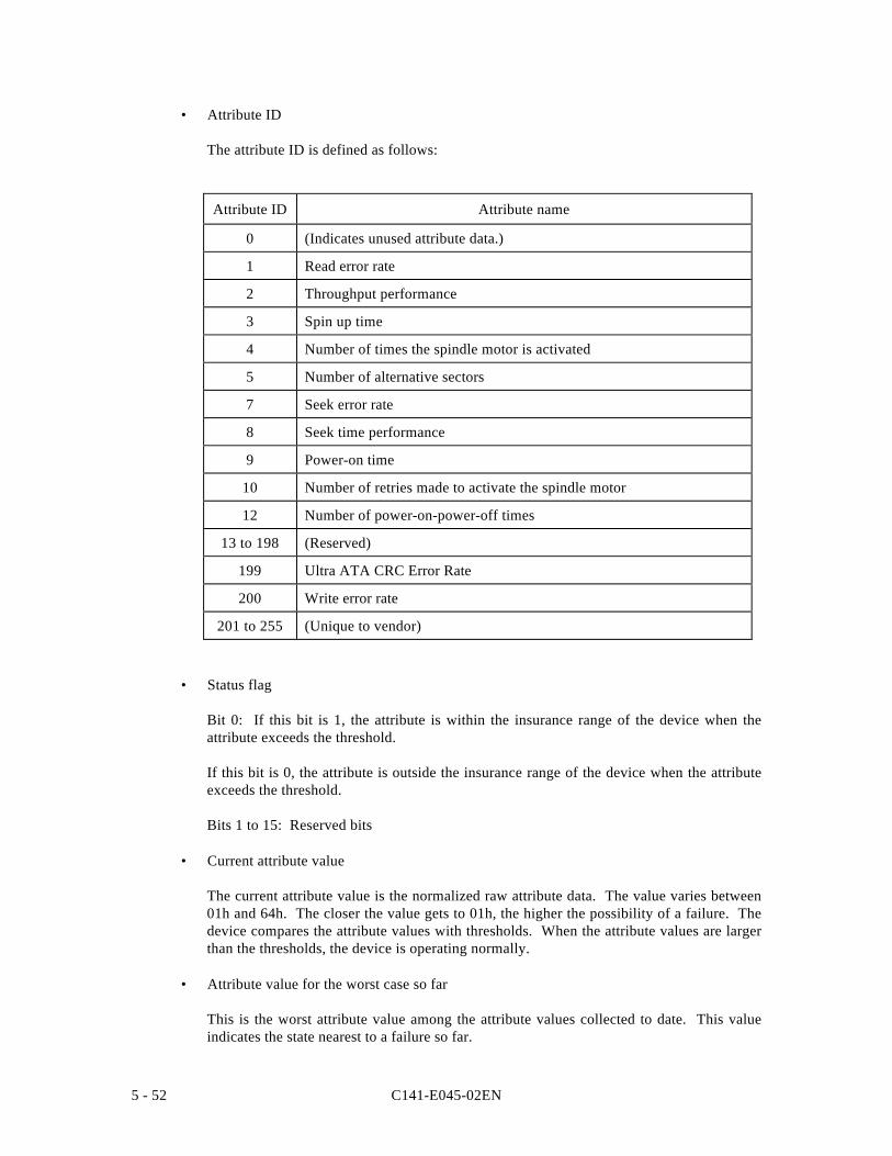
C141-E045-02EN5 - 52
• Attribute ID
The attribute ID is defined as follows:
Attribute ID Attribute name
0 (Indicates unused attribute data.)
1 Read error rate
2 Throughput performance
3 Spin up time
4 Number of times the spindle motor is activated
5 Number of alternative sectors
7 Seek error rate
8 Seek time performance
9 Power-on time
10 Number of retries made to activate the spindle motor
12 Number of power-on-power-off times
13 to 198 (Reserved)
199 Ultra ATA CRC Error Rate
200 Write error rate
201 to 255 (Unique to vendor)
• Status flag
Bit 0: If this bit is 1, the attribute is within the insurance range of the device when theattribute exceeds the threshold.
If this bit is 0, the attribute is outside the insurance range of the device when the attributeexceeds the threshold.
Bits 1 to 15: Reserved bits
• Current attribute value
The current attribute value is the normalized raw attribute data. The value varies between01h and 64h. The closer the value gets to 01h, the higher the possibility of a failure. Thedevice compares the attribute values with thresholds. When the attribute values are largerthan the thresholds, the device is operating normally.
• Attribute value for the worst case so far
This is the worst attribute value among the attribute values collected to date. This valueindicates the state nearest to a failure so far.
C141-E045-02EN 5 - 53
• Raw attribute value
Raw attributes data is retained.
• Failure prediction capability flag
Bit 0: The attribute value data is saved to a medium before the device enters power savingmode.
Bit 1: The device automatically saves the attribute value data to a medium after the previouslyset operation.
Bits 2 to 15: Reserved bits
• Check sum
Two's complement of the lower byte, obtained by adding 511-byte data one byte at a timefrom the beginning.
• Insurance failure threshold
The limit of a varying attribute value. The host compares the attribute values with thethresholds to identify a failure.
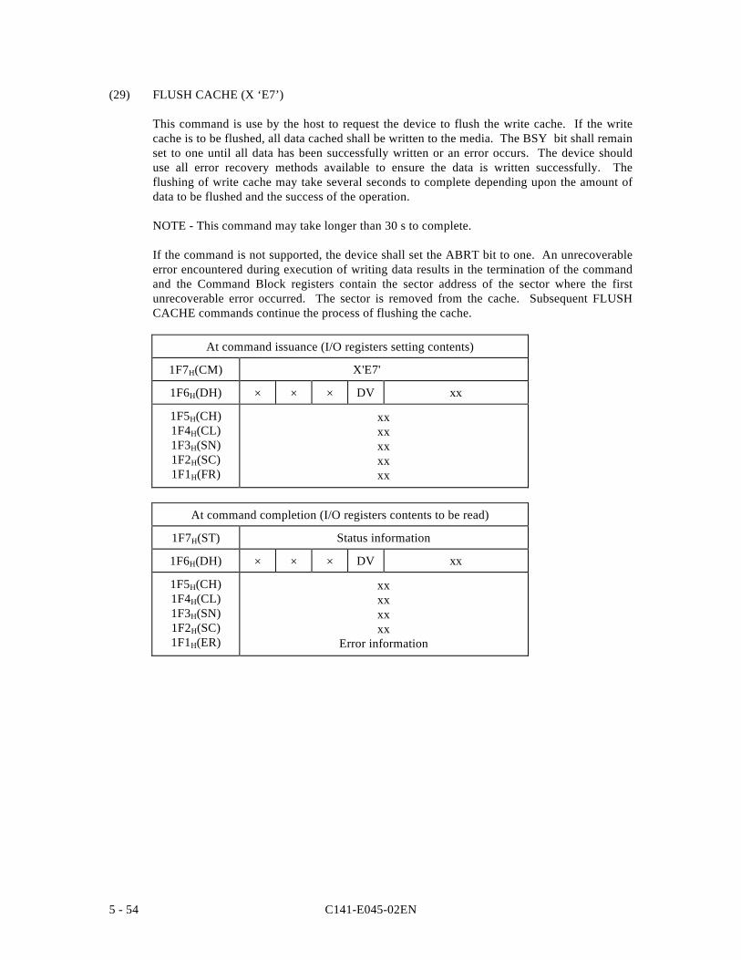
C141-E045-02EN5 - 54
(29) FLUSH CACHE (X ‘E7’)
This command is use by the host to request the device to flush the write cache. If the writecache is to be flushed, all data cached shall be written to the media. The BSY bit shall remainset to one until all data has been successfully written or an error occurs. The device shoulduse all error recovery methods available to ensure the data is written successfully. Theflushing of write cache may take several seconds to complete depending upon the amount ofdata to be flushed and the success of the operation.
NOTE - This command may take longer than 30 s to complete.
If the command is not supported, the device shall set the ABRT bit to one. An unrecoverableerror encountered during execution of writing data results in the termination of the commandand the Command Block registers contain the sector address of the sector where the firstunrecoverable error occurred. The sector is removed from the cache. Subsequent FLUSHCACHE commands continue the process of flushing the cache.
At command issuance (I/O registers setting contents)
1F7H(CM) X'E7'
1F6H(DH) × × × DV xx
1F5H(CH)1F4H(CL)1F3H(SN)1F2H(SC)1F1H(FR)
xxxxxxxxxx
At command completion (I/O registers contents to be read)
1F7H(ST) Status information
1F6H(DH) × × × DV xx
1F5H(CH)1F4H(CL)1F3H(SN)1F2H(SC)1F1H(ER)
xxxxxxxx
Error information
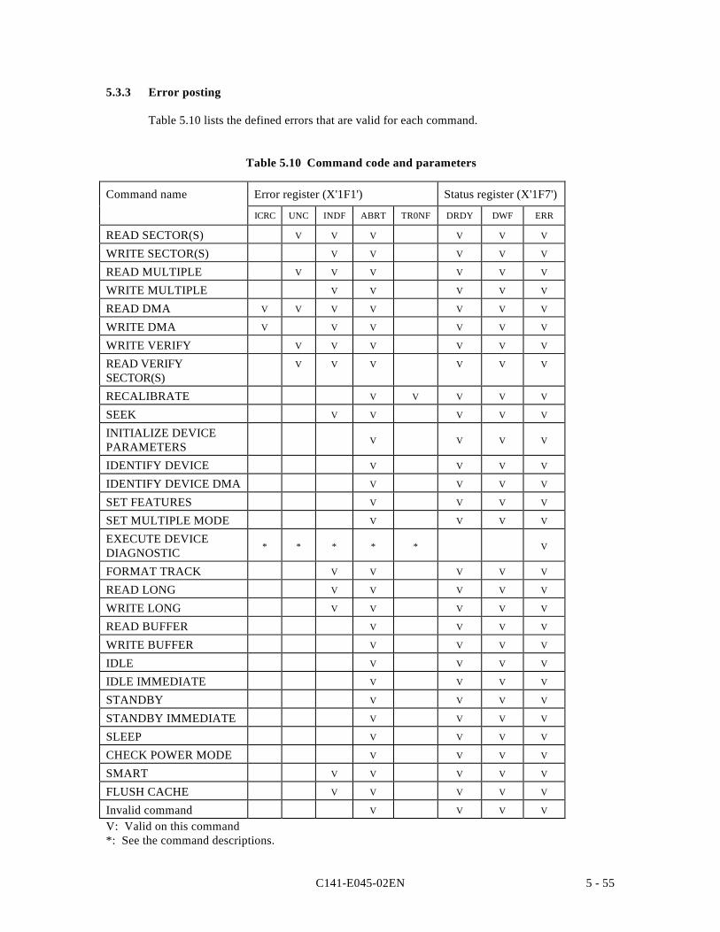
C141-E045-02EN 5 - 55
5.3.3 Error posting
Table 5.10 lists the defined errors that are valid for each command.
Table 5.10 Command code and parameters
Command name Error register (X'1F1') Status register (X'1F7')
ICRC UNC INDF ABRT TR0NF DRDY DWF ERR
READ SECTOR(S) V V V V V V
WRITE SECTOR(S) V V V V V
READ MULTIPLE V V V V V V
WRITE MULTIPLE V V V V V
READ DMA V V V V V V V
WRITE DMA V V V V V V
WRITE VERIFY V V V V V V
READ VERIFYSECTOR(S)
V V V V V V
RECALIBRATE V V V V V
SEEK V V V V V
INITIALIZE DEVICEPARAMETERS V V V V
IDENTIFY DEVICE V V V V
IDENTIFY DEVICE DMA V V V V
SET FEATURES V V V V
SET MULTIPLE MODE V V V V
EXECUTE DEVICEDIAGNOSTIC * * * * * V
FORMAT TRACK V V V V V
READ LONG V V V V V
WRITE LONG V V V V V
READ BUFFER V V V V
WRITE BUFFER V V V V
IDLE V V V V
IDLE IMMEDIATE V V V V
STANDBY V V V V
STANDBY IMMEDIATE V V V V
SLEEP V V V V
CHECK POWER MODE V V V V
SMART V V V V V
FLUSH CACHE V V V V V
Invalid command V V V V
V: Valid on this command*: See the command descriptions.
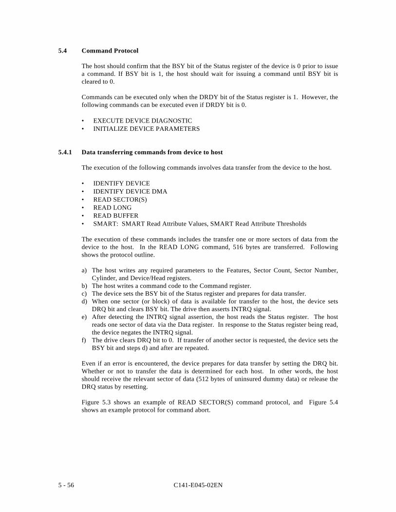
C141-E045-02EN5 - 56
5.4 Command Protocol
The host should confirm that the BSY bit of the Status register of the device is 0 prior to issuea command. If BSY bit is 1, the host should wait for issuing a command until BSY bit iscleared to 0.
Commands can be executed only when the DRDY bit of the Status register is 1. However, thefollowing commands can be executed even if DRDY bit is 0.
• EXECUTE DEVICE DIAGNOSTIC• INITIALIZE DEVICE PARAMETERS
5.4.1 Data transferring commands from device to host
The execution of the following commands involves data transfer from the device to the host.
• IDENTIFY DEVICE• IDENTIFY DEVICE DMA• READ SECTOR(S)• READ LONG• READ BUFFER• SMART: SMART Read Attribute Values, SMART Read Attribute Thresholds
The execution of these commands includes the transfer one or more sectors of data from thedevice to the host. In the READ LONG command, 516 bytes are transferred. Followingshows the protocol outline.
a) The host writes any required parameters to the Features, Sector Count, Sector Number,Cylinder, and Device/Head registers.
b) The host writes a command code to the Command register.c) The device sets the BSY bit of the Status register and prepares for data transfer.d) When one sector (or block) of data is available for transfer to the host, the device sets
DRQ bit and clears BSY bit. The drive then asserts INTRQ signal.e) After detecting the INTRQ signal assertion, the host reads the Status register. The host
reads one sector of data via the Data register. In response to the Status register being read,the device negates the INTRQ signal.
f) The drive clears DRQ bit to 0. If transfer of another sector is requested, the device sets theBSY bit and steps d) and after are repeated.
Even if an error is encountered, the device prepares for data transfer by setting the DRQ bit.Whether or not to transfer the data is determined for each host. In other words, the hostshould receive the relevant sector of data (512 bytes of uninsured dummy data) or release theDRQ status by resetting.
Figure 5.3 shows an example of READ SECTOR(S) command protocol, and Figure 5.4shows an example protocol for command abort.
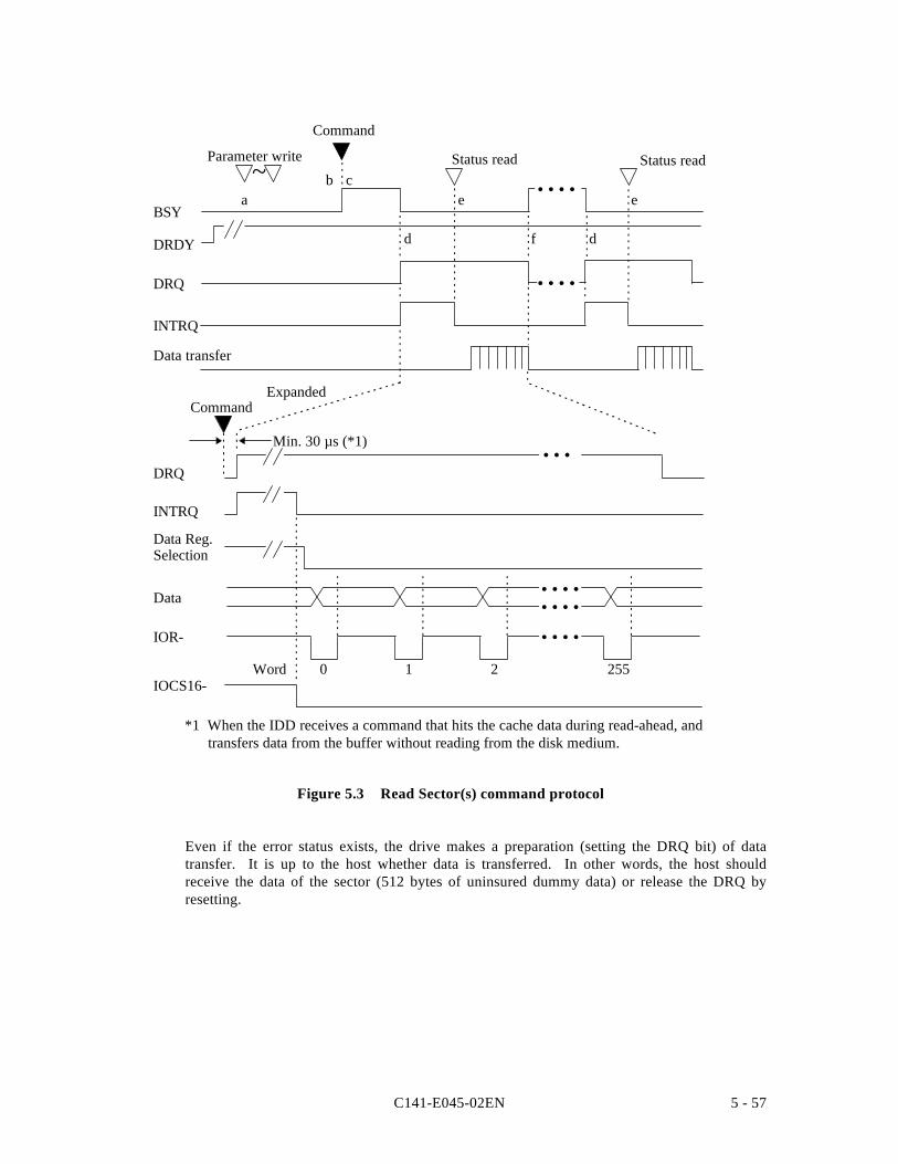
C141-E045-02EN 5 - 57
Status readStatus read
*1 When the IDD receives a command that hits the cache data during read-ahead, and transfers data from the buffer without reading from the disk medium.
255210WordIOCS16-
IOR-
Data
Data Reg.Selection
INTRQ
DRQ
Min. 30 µs (*1)
ExpandedCommand
f dd
eecb
a
Command
BSY
INTRQ
DRDY
~Parameter write
DRQ
Data transfer
• • • •
• • • •
• • •
• • • •• • • •
• • • •
Figure 5.3 Read Sector(s) command protocol
Even if the error status exists, the drive makes a preparation (setting the DRQ bit) of datatransfer. It is up to the host whether data is transferred. In other words, the host shouldreceive the data of the sector (512 bytes of uninsured dummy data) or release the DRQ byresetting.
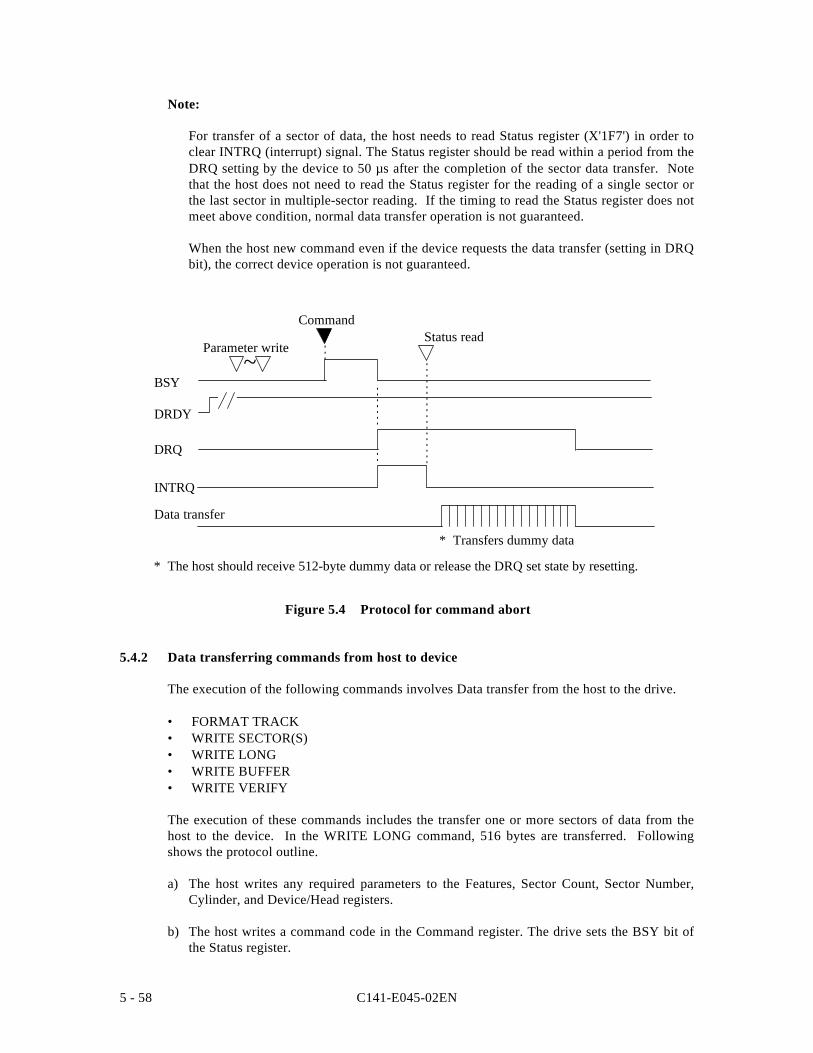
C141-E045-02EN5 - 58
Note:
For transfer of a sector of data, the host needs to read Status register (X'1F7') in order toclear INTRQ (interrupt) signal. The Status register should be read within a period from theDRQ setting by the device to 50 µs after the completion of the sector data transfer. Notethat the host does not need to read the Status register for the reading of a single sector orthe last sector in multiple-sector reading. If the timing to read the Status register does notmeet above condition, normal data transfer operation is not guaranteed.
When the host new command even if the device requests the data transfer (setting in DRQbit), the correct device operation is not guaranteed.
* Transfers dummy data
* The host should receive 512-byte dummy data or release the DRQ set state by resetting.
Status readCommand
BSY
INTRQ
DRDY
~Parameter write
DRQ
Data transfer
Figure 5.4 Protocol for command abort
5.4.2 Data transferring commands from host to device
The execution of the following commands involves Data transfer from the host to the drive.
• FORMAT TRACK• WRITE SECTOR(S)• WRITE LONG• WRITE BUFFER• WRITE VERIFY
The execution of these commands includes the transfer one or more sectors of data from thehost to the device. In the WRITE LONG command, 516 bytes are transferred. Followingshows the protocol outline.
a) The host writes any required parameters to the Features, Sector Count, Sector Number,Cylinder, and Device/Head registers.
b) The host writes a command code in the Command register. The drive sets the BSY bit ofthe Status register.
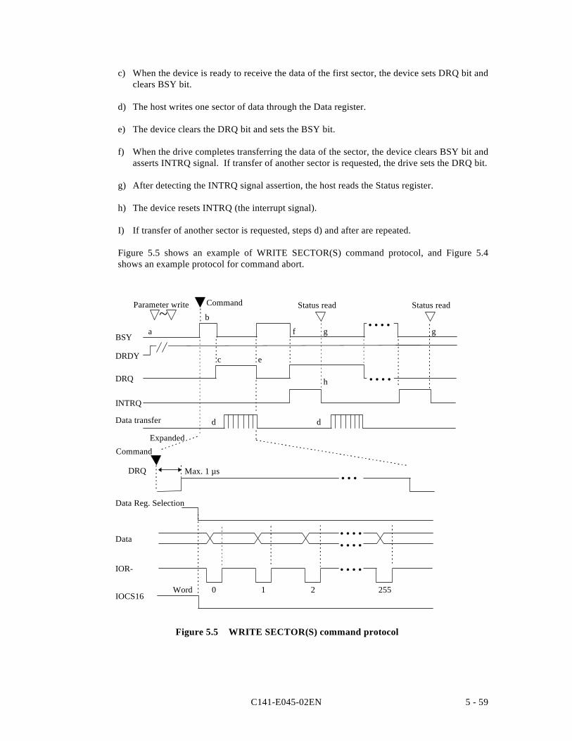
C141-E045-02EN 5 - 59
c) When the device is ready to receive the data of the first sector, the device sets DRQ bit andclears BSY bit.
d) The host writes one sector of data through the Data register.
e) The device clears the DRQ bit and sets the BSY bit.
f) When the drive completes transferring the data of the sector, the device clears BSY bit andasserts INTRQ signal. If transfer of another sector is requested, the drive sets the DRQ bit.
g) After detecting the INTRQ signal assertion, the host reads the Status register.
h) The device resets INTRQ (the interrupt signal).
I) If transfer of another sector is requested, steps d) and after are repeated.
Figure 5.5 shows an example of WRITE SECTOR(S) command protocol, and Figure 5.4shows an example protocol for command abort.
Status readStatus read
255210WordIOCS16
IOR-
Data
Data Reg. Selection
DRQ Max. 1 µs
Expanded
Command
ec
d d
h
ggf
b
a
Command
BSY
INTRQ
DRDY
~Parameter write
DRQ
Data transfer
• • • •
• • •
• • • •• • • •
• • • •
• • • •
Figure 5.5 WRITE SECTOR(S) command protocol
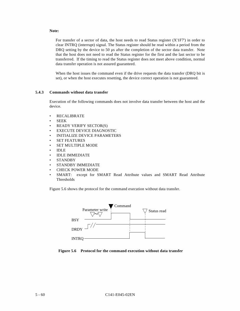
C141-E045-02EN5 - 60
Note:
For transfer of a sector of data, the host needs to read Status register (X'1F7') in order toclear INTRQ (interrupt) signal. The Status register should be read within a period from theDRQ setting by the device to 50 µs after the completion of the sector data transfer. Notethat the host does not need to read the Status register for the first and the last sector to betransferred. If the timing to read the Status register does not meet above condition, normaldata transfer operation is not assured guaranteed.
When the host issues the command even if the drive requests the data transfer (DRQ bit isset), or when the host executes resetting, the device correct operation is not guaranteed.
5.4.3 Commands without data transfer
Execution of the following commands does not involve data transfer between the host and thedevice.
• RECALIBRATE• SEEK• READY VERIFY SECTOR(S)• EXECUTE DEVICE DIAGNOSTIC• INITIALIZE DEVICE PARAMETERS• SET FEATURES• SET MULTIPLE MODE• IDLE• IDLE IMMEDIATE• STANDBY• STANDBY IMMEDIATE• CHECK POWER MODE• SMART: except for SMART Read Attribute values and SMART Read Attribute
Thresholds
Figure 5.6 shows the protocol for the command execution without data transfer.
Status readCommand
BSY
INTRQ
DRDY
~Parameter write
Figure 5.6 Protocol for the command execution without data transfer
C141-E045-02EN 5 - 61
5.4.4 Other commands
• READ MULTIPLE• SLEEP• WRITE MULTIPLE
See the description of each command.
5.4.5 DMA data transfer commands
• READ DMA• WRITE DMA
Starting the DMA transfer command is the same as the READ SECTOR(S) or WRITESECTOR(S) command except the point that the host initializes the DMA channel precedingthe command issuance.
The interrupt processing for the DMA transfer differs the following point.
• The interrupt processing for the DMA transfer differs the following point.
a) The host writes any parameters to the Features, Sector Count, Sector Number,Cylinder, and Device/Head register.
b) The host initializes the DMA channel
c) The host writes a command code in the Command register.
d) The device sets the BSY bit of the Status register.
e) The device asserts the DMARQ signal after completing the preparation of datatransfer. The device asserts either the BSY bit during DMA data transfer.
f) When the command execution is completed, the device clears both BSY and DRQbits and asserts the INTRQ signal. Then, the host reads the Status register.
g) The host resets the DMA channel.
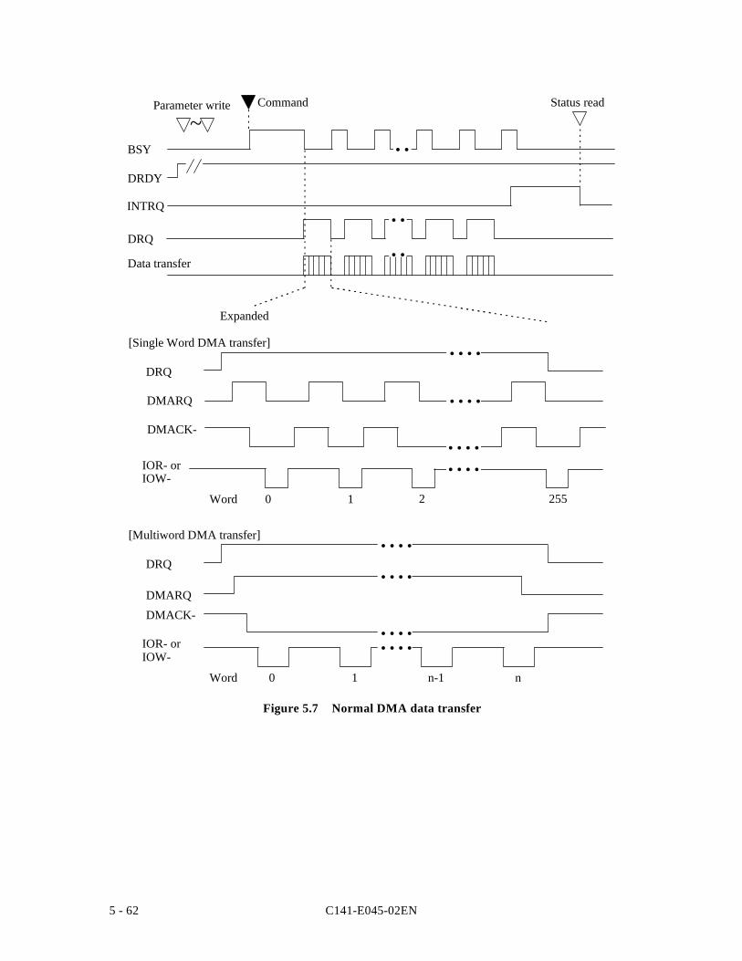
C141-E045-02EN5 - 62
Status read
255210Word
IOR- orIOW-
DMACK-
DMARQ
DRQ
Expanded
[Single Word DMA transfer]
Command
BSY
INTRQ
DRDY
~Parameter write
DRQ
Data transfer
• • • •
• •
• •
• • • •
• • • •• • • •
DRQ
[Multiword DMA transfer]• • • •
DMACK-
DMARQ• • • •
IOR- orIOW-
• • • •• • • •
0 1Word n-1 n
• •
Figure 5.7 Normal DMA data transfer
C141-E045-02EN 5 - 63
5.5 Ultra DMA feature set
5.5.1 Overview
Ultra DMA is a data transfer protocol used with the READ DMA and WRITE DMAcommands. When this protocol is enabled it shall be used instead of the Multiword DMAprotocol when these commands are issued by the host. This protocol applies to the UltraDMA data burst only. When this protocol is used there are no changes to other elements ofthe ATA protocol (e.g.: Command Block Register access).
Several signal lines are redefined to provide new functions during an Ultra DMA burst. Theselines assume these definitions when 1) an Ultra DMA Mode is selected, and 2) a host issues aREAD DMA or a WRITE DMA, command requiring data transfer, and 3) the host assertsDMACK-. These signal lines revert back to the definitions used for non-Ultra DMA transfersupon the negation of DMACK- by the host at the termination of an Ultra DMA burst. All ofthe control signals are unidirectional. DMARQ and DMACK- retain their standarddefinitions.
With the Ultra DMA protocol, the control signal (STROBE) that latches data from DD (15:0)is generated by the same agent (either host or device) that drives the data onto the bus.Ownership of DD (15:0) and this data strobe signal are given either to the device during anUltra DMA data in burst or to the host for an Ultra DMA data out burst.
During an Ultra DMA burst a sender shall always drive data onto the bus, and after a sufficienttime to allow for propagation delay, cable settling, and setup time, the sender shall generate aSTROBE edge to latch the data. Both edges of STROBE are used for data transfers so that thefrequency of STROBE is limited to the same frequency as the data. The highest fundamentalfrequency on the cable shall be 16.67 million transitions per second or 8.33 MHz (the same asthe maximum frequency for PIO Mode 4 and DMA Mode 2).
Words in the IDENTIFY DEVICE data indicate support of the Ultra DMA feature and theUltra DMA Modes the device is capable of supporting. The Set transfer mode subcommandin the SET FEATURES command shall be used by a host to select the Ultra DMA Mode atwhich the system operates. The Ultra DMA Mode selected by a host shall be less than orequal to the fastest mode of which the device is capable. Only the Ultra DMA Mode shall beselected at any given time. All timing requirements for a selected Ultra DMA Mode shall besatisfied. Devices supporting Ultra DMA Mode 2 shall also support Ultra DMA Modes 0 and1. Devices supporting Ultra DMA Mode 1 shall also support Ultra DMA Mode 0.
An Ultra DMA capable device shall retain its previously selected Ultra DMA Mode afterexecuting a Software reset sequence. An Ultra DMA capable device shall clear any previouslyselected Ultra DMA Mode and revert to its default non-Ultra DMA Modes after executing aPower on or hardware reset.
Both the host and device perform a CRC function during an Ultra DMA burst. At the end ofan Ultra DMA burst the host sends the its CRC data to the device. The device compares itsCRC data to the data sent from the host. If the two values do not match the device reports anerror in the error register at the end of the command. If an error occurs during one or moreUltra DMA bursts for any one command, at the end of the command, the device shall reportthe first error that occurred.
C141-E045-02EN5 - 64
5.5.2 Phases of operation
An Ultra DMA data transfer is accomplished through a series of Ultra DMA data in or data outbursts. Each Ultra DMA burst has three mandatory phases of operation: the initiation phase,the data transfer phase, and the Ultra DMA burst termination phase. In addition, an UltraDMA burst may be paused during the data transfer phase (see 5.5.3 and 5.5.4 for the detailedprotocol descriptions for each of these phases, 5.6.4 defines the specific timing requirements).In the following rules DMARDY- is used in cases that could apply to either DDMARDY- orHDMARDY-, and STROBE is used in cases that could apply to either DSTROBE orHSTROBE. The following are general Ultra DMA rules.
a) An Ultra DMA burst is defined as the period from an assertion of DMACK- by the host tothe subsequent negation of DMACK-.
b) A recipient shall be prepared to receive at least two data words whenever it enters orresumes an Ultra DMA burst.
5.5.3 Ultra DMA data in commands
5.5.3.1 Initiating an Ultra DMA data in burst
The following steps shall occur in the order they are listed unless otherwise specificallyallowed (see 5.6.4.1 and 5.6.4.2 for specific timing requirements):
1) The host shall keep DMACK- in the negated state before an Ultra DMA burst is initiated.
2) The device shall assert DMARQ to initiate an Ultra DMA burst. After assertion ofDMARQ the device shall not negate DMARQ until after the first negation of DSTROBE.
3) Steps (3), (4) and (5) may occur in any order or at the same time. The host shall assertSTOP.
4) The host shall negate HDMARDY-.
5) The host shall negate CS0-, CS1-, DA2, DA1, and DA0. The host shall keep CS0-, CS1-,DA2, DA1, and DA0 negated until after negating DMACK- at the end of the burst.
6) Steps (3), (4) and (5) shall have occurred at least tACK before the host asserts DMACK-.The host shall keep DMACK- asserted until the end of an Ultra DMA burst.
7) The host shall release DD (15:0) within tAZ after asserting DMACK-.
8) The device may assert DSTROBE tZIORDY after the host has asserted DMACK-. Once thedevice has driven DSTROBE the device shall not release DSTROBE until after the hosthas negated DMACK- at the end of an Ultra DMA burst.
9) The host shall negate STOP and assert HDMARDY- within tENV after asserting DMACK-.After negating STOP and asserting HDMARDY-, the host shall not change the state ofeither signal until after receiving the first transition of DSTROBE from the device (i.e.,after the first data word has been received).
10) The device shall drive DD (15:0) no sooner than tZAD after the host has asserted DMACK-,negated STOP, and asserted HDMARDY-.
C141-E045-02EN 5 - 65
11) The device shall drive the first word of the data transfer onto DD (15:0). This step mayoccur when the device first drives DD (15:0) in step (10).
12) To transfer the first word of data the device shall negate DSTROBE within tFS after thehost has negated STOP and asserted HDMARDY-. The device shall negate DSTROBE nosooner than tDVS after driving the first word of data onto DD (15:0).
5.5.3.2 The data in transfer
The following steps shall occur in the order they are listed unless otherwise specificallyallowed (see 5.6.4.3 and 5.6.4.2):
1) The device shall drive a data word onto DD (15:0).
2) The device shall generate a DSTROBE edge to latch the new word no sooner than tDVS
after changing the state of DD (15:0). The device shall generate a DSTROBE edge nomore frequently than tCYC for the selected Ultra DMA Mode. The device shall notgenerate two rising or two falling DSTROBE edges more frequently than 2tCYC for theselected Ultra DMA mode.
3) The device shall not change the state of DD (15:0) until at least tDVH after generating aDSTROBE edge to latch the data.
4) The device shall repeat steps (1), (2) and (3) until the data transfer is complete or an UltraDMA burst is paused, whichever occurs first.
5.5.3.3 Pausing an Ultra DMA data in burst
The following steps shall occur in the order they are listed unless otherwise specificallyallowed (see 5.6.4.4 and 5.6.4.2 for specific timing requirements).
a) Device pausing an Ultra DMA data in burst
1) The device shall not pause an Ultra DMA burst until at least one data word of an UltraDMA burst has been transferred.
2) The device shall pause an Ultra DMA burst by not generating DSTROBE edges.
NOTE - The host shall not immediately assert STOP to initiate Ultra DMA bursttermination when the device stops generating STROBE edges. If the device does notnegate DMARQ, in order to initiate ULTRA DMA burst termination, the host shallnegate HDMARDY- and wait tRP before asserting STOP.
3) The device shall resume an Ultra DMA burst by generating a DSTROBE edge.
b) Host pausing an Ultra DMA data in burst
1) The host shall not pause an Ultra DMA burst until at least one data word of an UltraDMA burst has been transferred.
2) The host shall pause an Ultra DMA burst by negating HDMARDY-.
C141-E045-02EN5 - 66
3) The device shall stop generating DSTROBE edges within tRFS of the host negatingHDMARDY-.
4) If the host negates HDMARDY- within tSR after the device has generated aDSTROBE edge, then the host shall be prepared to receive zero or one additional datawords. If the host negates HDMARDY- greater than tSR after the device hasgenerated a DSTROBE edge, then the host shall be prepared to receive zero, one ortwo additional data words. The additional data words are a result of cable round tripdelay and tRFS timing for the device.
5) The host shall resume an Ultra DMA burst by asserting HDMARDY-.
5.5.3.4 Terminating an Ultra DMA data in burst
a) Device terminating an Ultra DMA data in burst
The following steps shall occur in the order they are listed unless otherwise specificallyallowed (see 5.6.4.5 and 5.6.4.2 for specific timing requirements):
1) The device shall initiate termination of an Ultra DMA burst by not generatingDSTROBE edges.
2) The device shall negate DMARQ no sooner than tSS after generating the lastDSTROBE edge. The device shall not assert DMARQ again until after the UltraDMA burst is terminated.
3) The device shall release DD (15:0) no later than tAZ after negating DMARQ.
4) The host shall assert STOP within tLI after the device has negated DMARQ. The hostshall not negate STOP again until after the Ultra DMA burst is terminated.
5) The host shall negate HDMARDY- within tLI after the device has negated DMARQ.The host shall continue to negate HDMARDY- until the Ultra DMA burst isterminated. Steps (4) and (5) may occur at the same time.
6) The host shall drive DD (15:0) no sooner than tZAH after the device has negatedDMARQ. For this step, the host may first drive DD (15:0) with the result of its CRCcalculation (see 5.5.5):
7) If DSTROBE is negated, the device shall assert DSTROBE within tLI after the hosthas asserted STOP. No data shall be transferred during this assertion. The host shallignore this transition on DSTROBE. DSTROBE shall remain asserted until the UltraDMA burst is terminated.
8) If the host has not placed the result of its CRC calculation on DD (15:0) since firstdriving DD (15:0) during (6), the host shall place the result of its CRC calculation onDD (15:0) (see 5.5.5).
9) The host shall negate DMACK- no sooner than tMLI after the device has assertedDSTROBE and negated DMARQ and the host has asserted STOP and negatedHDMARDY-, and no sooner than tDVS after the host places the result of its CRCcalculation on DD (15:0).
C141-E045-02EN 5 - 67
10) The device shall latch the host's CRC data from DD (15:0) on the negating edge ofDMACK-.
11) The device shall compare the CRC data received from the host with the results of itsown CRC calculation. If a miscompare error occurs during one or more Ultra DMAbursts for any one command, at the end of the command the device shall report thefirst error that occurred (see 5.5.5).
12) The device shall release DSTROBE within tIORDYZ after the host negates DMACK-.
13) The host shall not negate STOP no assert HDMARDY- until at least tACK afternegating DMACK-.
14) The host shall not assert DIOR-, CS0-, CS1-, DA2, DA1, or DA0 until at least tACK
after negating DMACK.
b) Host terminating an Ultra DMA data in burst
The following steps shall occur in the order they are listed unless otherwise specificallyallowed (see 5.6.4.6 and 5.6.4.2 for specific timing requirements):
1) The host shall not initiate Ultra DMA burst termination until at least one data word ofan Ultra DMA burst has been transferred.
2) The host shall initiate Ultra DMA burst termination by negating HDMARDY-. Thehost shall continue to negate HDMARDY- until the Ultra DMA burst is terminated.
3) The device shall stop generating DSTROBE edges within tRFS of the host negatingHDMARDY-.
4) If the host negates HDMARDY- within tSR after the device has generated aDSTROBE edge, then the host shall be prepared to receive zero or one additional datawords. If the host negates HDMARDY- greater than tSR after the device hasgenerated a DSTROBE edge, then the host shall be prepared to receive zero, one ortwo additional data words. The additional data words are a result of cable round tripdelay and tRFS timing for the device.
5) The host shall assert STOP no sooner than tRP after negating HDMARDY-. The hostshall not negate STOP again until after the Ultra DMA burst is terminated.
6) The device shall negate DMARQ within tLI after the host has asserted STOP. Thedevice shall not assert DMARQ again until after the Ultra DMA burst is terminated.
7) If DSTROBE is negated, the device shall assert DSTROBE within tLI after the hosthas asserted STOP. No data shall be transferred during this assertion. The host shallignore this transition on DSTROBE. DSTROBE shall remain asserted until the UltraDMA burst is terminated.
8) The device shall release DD (15:0) no later than tAZ after negating DMARQ.
9) The host shall drive DD (15:0) no sooner than tZAH after the device has negatedDMARQ. For this step, the host may first drive DD (15:0) with the result of its CRCcalculation (see 5.5.5).
C141-E045-02EN5 - 68
10) If the host has not placed the result of its CRC calculation on DD (15:0) since firstdriving DD (15:0) during (9), the host shall place the result of its CRC calculation onDD (15:0) (see 5.5.5).
11) The host shall negate DMACK- no sooner than tMLI after the device has assertedDSTROBE and negated DMARQ and the host has asserted STOP and negatedHDMARDY-, and no sooner than tDVS after the host places the result of its CRCcalculation on DD (15:0).
12) The device shall latch the host's CRC data from DD (15:0) on the negating edge ofDMACK-.
13) The device shall compare the CRC data received from the host with the results of itsown CRC calculation. If a miscompare error occurs during one or more Ultra DMAburst for any one command, at the end of the command, the device shall report thefirst error that occurred (see 5.5.5).
14) The device shall release DSTROBE within tIORDYZ after the host negates DMACK-.
15) The host shall neither negate STOP nor assert HDMARDY- until at least tACK after thehost has negated DMACK-.
16) The host shall not assert DIOR-, CS0-, CS1-, DA2, DA1, or DA0 until at least tACK
after negating DMACK.
5.5.4 Ultra DMA data out commands
5.5.4.1 Initiating an Ultra DMA data out burst
The following steps shall occur in the order they are listed unless otherwise specificallyallowed (see 5.6.4.7 and 5.6.4.2 for specific timing requirements):
1) The host shall keep DMACK- in the negated state before an Ultra DMA burst is initiated.
2) The device shall assert DMARQ to initiate an Ultra DMA burst.
3) Steps (3), (4), and (5) may occur in any order or at the same time. The host shall assertSTOP.
4) The host shall assert HSTROBE.
5) The host shall negate CS0-, CS1-, DA2, DA1, and DA0. The host shall keep CS0-, CS1-,DA2, DA1, and DA0 negated until after negating DMACK- at the end of the burst.
6) Steps (3), (4), and (5) shall have occurred at least tACK before the host asserts DMACK-.The host shall keep DMACK- asserted until the end of an Ultra DMA burst.
7) The device may negate DDMARDY- tZIORDY after the host has asserted DMACK-. Oncethe device has negated DDMARDY-, the device shall not release DDMARDY- until afterthe host has negated DMACK- at the end of an Ultra DMA burst.
8) The host shall negate STOP within tENV after asserting DMACK-. The host shall not assertSTOP until after the first negation of HSTROBE.
C141-E045-02EN 5 - 69
9) The device shall assert DDMARDY- within tLI after the host has negated STOP. Afterasserting DMARQ and DDMARDY- the device shall not negate either signal until afterthe first negation of HSTROBE by the host.
10) The host shall drive the first word of the data transfer onto DD (15:0). This step mayoccur any time during Ultra DMA burst initiation.
11) To transfer the first word of data: the host shall negate HSTROBE no sooner than tLI afterthe device has asserted DDMARDY-. The host shall negate HSTROBE no sooner thantDVS after the driving the first word of data onto DD (15:0).
5.5.4.2 The data out transfer
The following steps shall occur in the order they are listed unless otherwise specificallyallowed (see 5.6.4.8 and 5.6.4.2 for specific timing requirements):
1) The host shall drive a data word onto DD (15:0).
2) The host shall generate an HSTROBE edge to latch the new word no sooner than tDVS afterchanging the state of DD (15:0). The host shall generate an HSTROBE edge no morefrequently than tCYC for the selected Ultra DMA Mode. The host shall not generate tworising or falling HSTROBE edges more frequently than 2 tCYC for the selected Ultra DMAmode.
3) The host shall not change the state of DD (15:0) until at least tDVH after generating anHSTROBE edge to latch the data.
4) The host shall repeat steps (1), (2) and (3) until the data transfer is complete or an UltraDMA burst is paused, whichever occurs first.
5.5.4.3 Pausing an Ultra DMA data out burst
The following steps shall occur in the order they are listed unless otherwise specificallyallowed (see 5.6.4.9 and 5.6.4.2 for specific timing requirements).
a) Host pausing an Ultra DMA data out burst
1) The host shall not pause an Ultra DMA burst until at least one data word of an UltraDMA burst has been transferred.
2) The host shall pause an Ultra DMA burst by not generating an HSTROBE edge.
Note: The device shall not immediately negate DMARQ to initiate Ultra DMA bursttermination when the host stops generating HSTROBE edges. If the host does notassert STOP, in order to initiate Ultra DMA burst termination, the device shall negateDDMARDY- and wait tRP before negating DMARQ.
3) The host shall resume an Ultra DMA burst by generating an HSTROBE edge.
C141-E045-02EN5 - 70
b) Device pausing an Ultra DMA data out burst
1) The device shall not pause an Ultra DMA burst until at least one data word of an UltraDMA burst has been transferred.
2) The device shall pause an Ultra DMA burst by negating DDMARDY-.
3) The host shall stop generating HSTROBE edges within tRFS of the device negatingDDMARDY-.
4) If the device negates DDMARDY- within tSR after the host has generated anHSTROBE edge, then the device shall be prepared to receive zero or one additionaldata words. If the device negates DDMARDY- greater than tSR after the host hasgenerated an HSTROBE edge, then the device shall be prepared to receive zero, oneor two additional data words. The additional data words are a result of cable roundtrip delay and tRFS timing for the host.
5) The device shall resume an Ultra DMA burst by asserting DDMARDY-.
5.5.4.4 Terminating an Ultra DMA data out burst
a) Host terminating an Ultra DMA data out burst
The following stops shall occur in the order they are listed unless otherwise specificallyallowed (see 5.6.4.10 and 5.6.4.2 for specific timing requirements):
1) The host shall initiate termination of an Ultra DMA burst by not generatingHSTROBE edges.
2) The host shall assert STOP no sooner than tSS after it last generated an HSTROBEedge. The host shall not negate STOP again until after the Ultra DMA burst isterminated.
3) The device shall negate DMARQ within tLI after the host asserts STOP. The deviceshall not assert DMARQ again until after the Ultra DMA burst is terminated.
4) The device shall negate DDMARDY- with tLI after the host has negated STOP. Thedevice shall not assert DDMARDY- again until after the Ultra DMA burst terminationis complete.
5) If HSTROBE is negated, the host shall assert HSTROBE with tLI after the device hasnegated DMARQ. No data shall be transferred during this assertion. The device shallignore this transition on HSTROBE. HSTROBE shall remain asserted until the UltraDMA burst is terminated.
6) The host shall place the result of its CRC calculation on DD (15:0) (see 5.5.5)
7) The host shall negate DMACK- no sooner than tMLI after the host has assertedHSTROBE and STOP and the device has negated DMARQ and DDMARDY-, and nosooner than tDVS after placing the result of its CRC calculation on DD (15:0).
8) The device shall latch the host's CRC data from DD (15:0) on the negating edge ofDMACK-.
C141-E045-02EN 5 - 71
9) The device shall compare the CRC data received from the host with the results of itsown CRC calculation. If a miscompare error occurs during one or more Ultra DMAbursts for any one command, at the end of the command, the device shall report thefirst error that occurred (see 5.5.5).
10) The device shall release DDMARDY- within tIORDYZ after the host has negatedDMACK-.
11) The host shall neither negate STOP nor negate HSTROBE until at least tACK afternegating DMACK-.
12) The host shall not assert DIOW-, CS0-, CS1-, DA2, DA1, or DA0 until at least tACK
after negating DMACK.
b) Device terminating an Ultra DMA data out burst
The following steps shall occur in the order they are listed unless otherwise specificallyallowed (see 5.6.4.11 and 5.6.4.2 for specific timing requirements):
1) The device shall not initiate Ultra DMA burst termination until at least one data wordof an Ultra DMA burst has been transferred.
2) The device shall initiate Ultra DMA burst termination by negating DDMARDY-.
3) The host shall stop generating an HSTROBE edges within tRFS of the device negatingDDMARDY-.
4) If the device negates DDMARDY- within tSR after the host has generated anHSTROBE edge, then the device shall be prepared to receive zero or one additionaldata words. If the device negates DDMARDY- greater than tSR after the host hasgenerated an HSTROBE edge, then the device shall be prepared to receive zero, oneor two additional data words. The additional data words are a result of cable roundtrip delay and tRFS timing for the host.
5) The device shall negate DMARQ no sooner than tRP after negating DDMARDY-.The device shall not assert DMARQ again until after the Ultra DMA burst isterminated.
6) The host shall assert STOP with tLI after the device has negated DMARQ. The hostshall not negate STOP again until after the Ultra DMA burst is terminated.
7) If HSTROBE is negated, the host shall assert HSTROBE with tLI after the device hasnegated DMARQ. No data shall be transferred during this assertion. The device shallignore this transition of HSTROBE. HSTROBE shall remain asserted until the UltraDMA burst is terminated.
8) The host shall place the result of its CRC calculation on DD (15:0) (see 5.5.5).
9) The host shall negate DMACK- no sooner than tMLI after the host has assertedHSTROBE and STOP and the device has negated DMARQ and DDMARDY-, and nosooner than tDVS after placing the result of its CRC calculation on DD (15:0).
10) The device shall latch the host's CRC data from DD (15:0) on the negating edge ofDMACK-.
C141-E045-02EN5 - 72
11) The device shall compare the CRC data received from the host with the results of itsown CRC calculation. If a miscompare error occurs during one or more Ultra DMAbursts for any one command, at the end of the command, the device shall report thefirst error that occurred (see 5.5.5).
12) The device shall release DDMARDY- within tIORDYZ after the host has negated DMACK-.
13) The host shall neither negate STOP nor HSTROBE until at least tACK after negatingDMACK-.
14) The host shall not assert DIOW-, CS0-, CS1-, DA2, DA1, or DA0 until at least tACK
after negating DMACK.
5.5.5 Ultra DMA CRC rules
The following is a list of rules for calculating CRC, determining if a CRC error has occurredduring an Ultra DMA burst, and reporting any error that occurs at the end of a command.
a) Both the host and the device shall have a 16-bit CRC calculation function.
b) Both the host and the device shall calculate a CRC value for each Ultra DMA burst.
c) The CRC function in the host and the device shall be initialized with a seed of 4ABAh atthe beginning of an Ultra DMA burst before any data is transferred.
d) For each STROBE transition used for data transfer, both the host and the device shallcalculate a new CRC value by applying the CRC polynomial to the current value of theirindividual CRC functions and the word being transferred. CRC is not calculated for thereturn of STROBE to the asserted state after the Ultra DMA burst termination request hasbeen acknowledged.
e) At the end of any Ultra DMA burst the host shall send the results of its CRC calculationfunction to the device on DD (15:0) with the negation of DMACK-.
f) The device shall then compare the CRC data from the host with the calculated value in itsown CRC calculation function. If the two values do not match, the device shall save theerror and report it at the end of the command. A subsequent Ultra DMA burst for the samecommand that does not have a CRC error shall not clear an error saved from a previousUltra DMa burst in the same command. If a miscompare error occurs during one or moreUltra DMA bursts for any one command, at the end of the command, the device shallreport the first error that occurred.
g) For READ DMA or WRITE DMA commands: When a CRC error is detected, it shall bereported by setting both ICRC and ABRT (bit 7 and bit 2 in the Error register) to one.ICRC is defined as the "Interface CRC Error" bit. The host shall respond to this error byre-issuing the command.
h) A host may send extra data words on the last Ultra DMA burst of a data out command. Ifa device determines that all data has been transferred for a command, the device shallterminate the burst. A device may have already received more data words than wererequired for the command. These extra words are used by both the host and the device tocalculate the CRC, but, on an Ultra DMA data out burst, the extra words shall be discardedby the device.
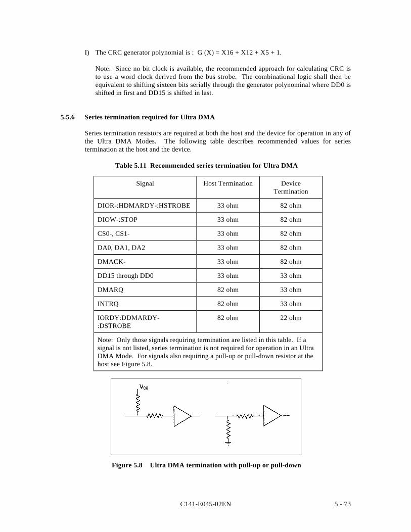
C141-E045-02EN 5 - 73
I) The CRC generator polynomial is : G (X) = X16 + X12 + X5 + 1.
Note: Since no bit clock is available, the recommended approach for calculating CRC isto use a word clock derived from the bus strobe. The combinational logic shall then beequivalent to shifting sixteen bits serially through the generator polynominal where DD0 isshifted in first and DD15 is shifted in last.
5.5.6 Series termination required for Ultra DMA
Series termination resistors are required at both the host and the device for operation in any ofthe Ultra DMA Modes. The following table describes recommended values for seriestermination at the host and the device.
Table 5.11 Recommended series termination for Ultra DMA
Signal Host Termination DeviceTermination
DIOR-:HDMARDY-:HSTROBE 33 ohm 82 ohm
DIOW-:STOP 33 ohm 82 ohm
CS0-, CS1- 33 ohm 82 ohm
DA0, DA1, DA2 33 ohm 82 ohm
DMACK- 33 ohm 82 ohm
DD15 through DD0 33 ohm 33 ohm
DMARQ 82 ohm 33 ohm
INTRQ 82 ohm 33 ohm
IORDY:DDMARDY-:DSTROBE
82 ohm 22 ohm
Note: Only those signals requiring termination are listed in this table. If asignal is not listed, series termination is not required for operation in an UltraDMA Mode. For signals also requiring a pull-up or pull-down resistor at thehost see Figure 5.8.
Figure 5.8 Ultra DMA termination with pull-up or pull-down

C141-E045-02EN5 - 74
5.6 Timing
5.6.1 PIO data transfer
Figure 5.9 shows of the data transfer timing between the device and the host system.
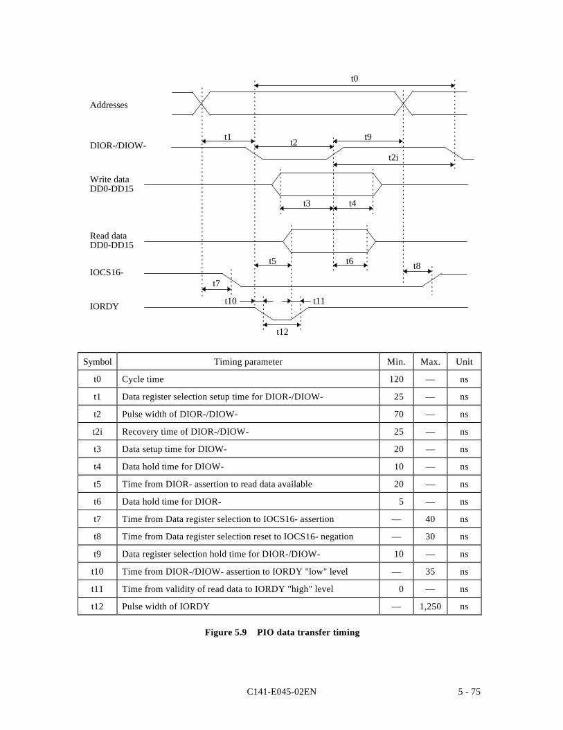
C141-E045-02EN 5 - 75
t8t6
t12
t11t10
t7
t5
t4t3
t9
t2i
t2t1
t0
Addresses
IORDY
IOCS16-
Read dataDD0-DD15
Write dataDD0-DD15
DIOR-/DIOW-
Symbol Timing parameter Min. Max. Unit
t0 Cycle time 120 — ns
t1 Data register selection setup time for DIOR-/DIOW- 25 — ns
t2 Pulse width of DIOR-/DIOW- 70 — ns
t2i Recovery time of DIOR-/DIOW- 25 — ns
t3 Data setup time for DIOW- 20 — ns
t4 Data hold time for DIOW- 10 — ns
t5 Time from DIOR- assertion to read data available 20 — ns
t6 Data hold time for DIOR- 5 — ns
t7 Time from Data register selection to IOCS16- assertion — 40 ns
t8 Time from Data register selection reset to IOCS16- negation — 30 ns
t9 Data register selection hold time for DIOR-/DIOW- 10 — ns
t10 Time from DIOR-/DIOW- assertion to IORDY "low" level — 35 ns
t11 Time from validity of read data to IORDY "high" level 0 — ns
t12 Pulse width of IORDY — 1,250 ns
Figure 5.9 PIO data transfer timing
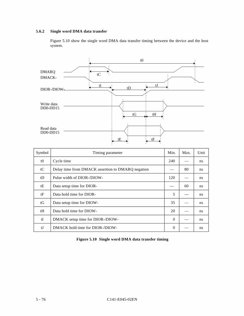
C141-E045-02EN5 - 76
5.6.2 Single word DMA data transfer
Figure 5.10 show the single word DMA data transfer timing between the device and the hostsystem.
tFtE
tHtG
tJtDtI
tC
t0
Read dataDD0-DD15
Write dataDD0-DD15
DIOR-/DIOW-
DMACK-DMARQ
Symbol Timing parameter Min. Max. Unit
t0 Cycle time 240 — ns
tC Delay time from DMACK assertion to DMARQ negation — 80 ns
tD Pulse width of DIOR-/DIOW- 120 — ns
tE Data setup time for DIOR- — 60 ns
tF Data hold time for DIOR- 5 — ns
tG Data setup time for DIOW- 35 — ns
tH Data hold time for DIOW- 20 — ns
tI DMACK setup time for DIOR-/DIOW- 0 — ns
tJ DMACK hold time for DIOR-/DIOW- 0 — ns
Figure 5.10 Single word DMA data transfer timing
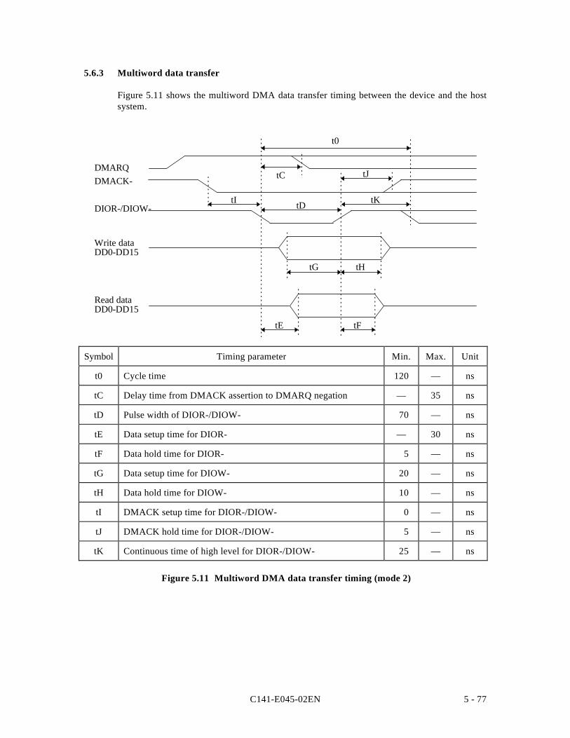
C141-E045-02EN 5 - 77
5.6.3 Multiword data transfer
Figure 5.11 shows the multiword DMA data transfer timing between the device and the hostsystem.
tFtE
tHtG
tJ
tDtI
tC
t0
Read dataDD0-DD15
Write dataDD0-DD15
DIOR-/DIOW-
DMACK-DMARQ
tK
Symbol Timing parameter Min. Max. Unit
t0 Cycle time 120 — ns
tC Delay time from DMACK assertion to DMARQ negation — 35 ns
tD Pulse width of DIOR-/DIOW- 70 — ns
tE Data setup time for DIOR- — 30 ns
tF Data hold time for DIOR- 5 — ns
tG Data setup time for DIOW- 20 — ns
tH Data hold time for DIOW- 10 — ns
tI DMACK setup time for DIOR-/DIOW- 0 — ns
tJ DMACK hold time for DIOR-/DIOW- 5 — ns
tK Continuous time of high level for DIOR-/DIOW- 25 — ns
Figure 5.11 Multiword DMA data transfer timing (mode 2)
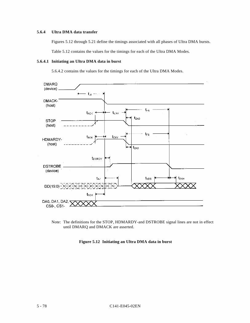
C141-E045-02EN5 - 78
5.6.4 Ultra DMA data transfer
Figures 5.12 through 5.21 define the timings associated with all phases of Ultra DMA bursts.
Table 5.12 contains the values for the timings for each of the Ultra DMA Modes.
5.6.4.1 Initiating an Ultra DMA data in burst
5.6.4.2 contains the values for the timings for each of the Ultra DMA Modes.
Note: The definitions for the STOP, HDMARDY-and DSTROBE signal lines are not in effectuntil DMARQ and DMACK are asserted.
Figure 5.12 Initiating an Ultra DMA data in burst
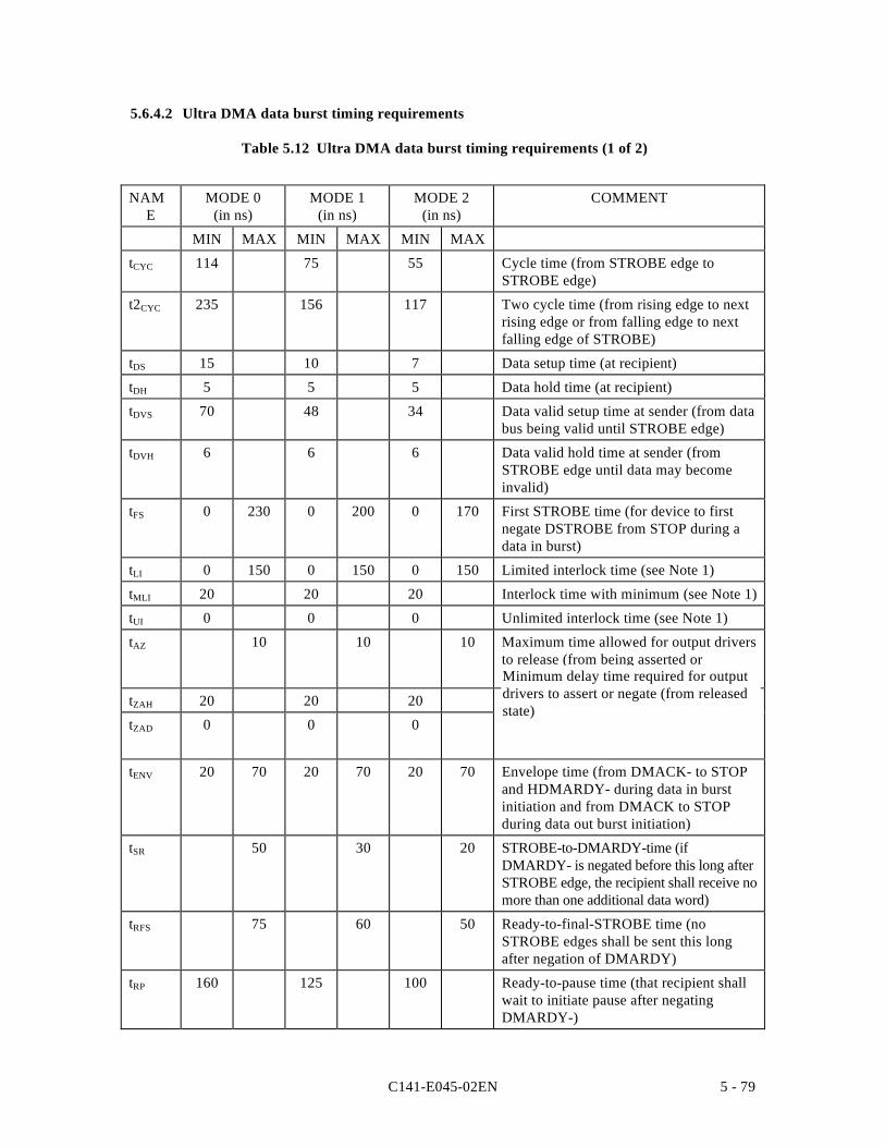
C141-E045-02EN 5 - 79
5.6.4.2 Ultra DMA data burst timing requirements
Table 5.12 Ultra DMA data burst timing requirements (1 of 2)
NAME
MODE 0(in ns)
MODE 1(in ns)
MODE 2(in ns)
COMMENT
MIN MAX MIN MAX MIN MAX
tCYC 114 75 55 Cycle time (from STROBE edge toSTROBE edge)
t2CYC 235 156 117 Two cycle time (from rising edge to nextrising edge or from falling edge to nextfalling edge of STROBE)
tDS 15 10 7 Data setup time (at recipient)
tDH 5 5 5 Data hold time (at recipient)
tDVS 70 48 34 Data valid setup time at sender (from databus being valid until STROBE edge)
tDVH 6 6 6 Data valid hold time at sender (fromSTROBE edge until data may becomeinvalid)
tFS 0 230 0 200 0 170 First STROBE time (for device to firstnegate DSTROBE from STOP during adata in burst)
tLI 0 150 0 150 0 150 Limited interlock time (see Note 1)
tMLI 20 20 20 Interlock time with minimum (see Note 1)
tUI 0 0 0 Unlimited interlock time (see Note 1)
tAZ 10 10 10 Maximum time allowed for output driversto release (from being asserted ornegated)
tZAH 20 20 20
tZAD 0 0 0
tENV 20 70 20 70 20 70 Envelope time (from DMACK- to STOPand HDMARDY- during data in burstinitiation and from DMACK to STOPduring data out burst initiation)
tSR 50 30 20 STROBE-to-DMARDY-time (ifDMARDY- is negated before this long afterSTROBE edge, the recipient shall receive nomore than one additional data word)
tRFS 75 60 50 Ready-to-final-STROBE time (noSTROBE edges shall be sent this longafter negation of DMARDY)
tRP 160 125 100 Ready-to-pause time (that recipient shallwait to initiate pause after negatingDMARDY-)
Minimum delay time required for outputdrivers to assert or negate (from releasedstate)
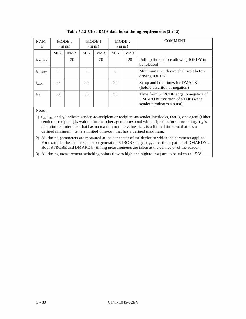
C141-E045-02EN5 - 80
Table 5.12 Ultra DMA data burst timing requirements (2 of 2)
NAME
MODE 0(in ns)
MODE 1(in ns)
MODE 2(in ns)
COMMENT
MIN MAX MIN MAX MIN MAX
tIORDYZ 20 20 20 Pull-up time before allowing IORDY tobe released
tZIORDY 0 0 0 Minimum time device shall wait beforedriving IORDY
tACK 20 20 20 Setup and hold times for DMACK-(before assertion or negation)
tSS 50 50 50 Time from STROBE edge to negation ofDMARQ or assertion of STOP (whensender terminates a burst)
Notes:
1) tUI, tMLI and tLI indicate sender -to-recipient or recipient-to-sender interlocks, that is, one agent (eithersender or recipient) is waiting for the other agent to respond with a signal before proceeding. tUI isan unlimited interlock, that has no maximum time value. tMLI is a limited time-out that has adefined minimum. tLI is a limited time-out, that has a defined maximum.
2) All timing parameters are measured at the connector of the device to which the parameter applies.For example, the sender shall stop generating STROBE edges tRFS after the negation of DMARDY-.Both STROBE and DMARDY- timing measurements are taken at the connector of the sender.
3) All timing measurement switching points (low to high and high to low) are to be taken at 1.5 V.
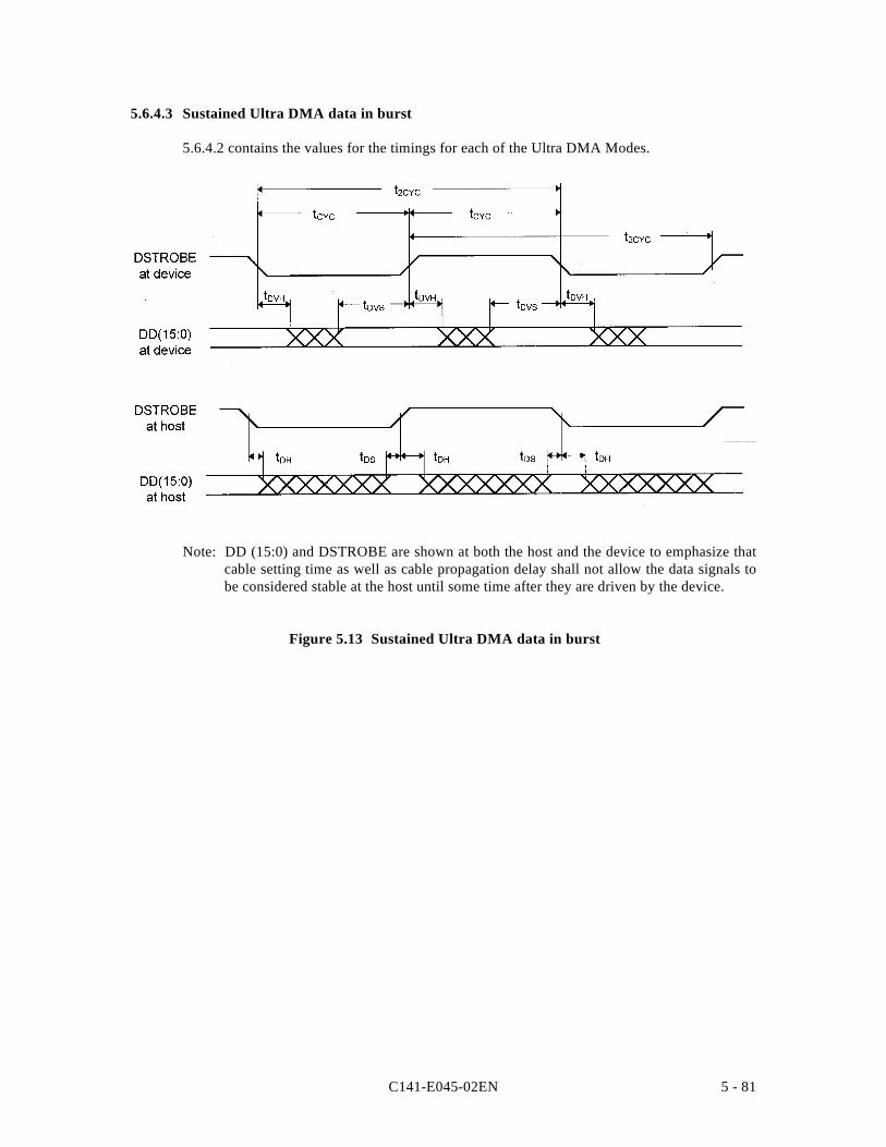
C141-E045-02EN 5 - 81
5.6.4.3 Sustained Ultra DMA data in burst
5.6.4.2 contains the values for the timings for each of the Ultra DMA Modes.
Note: DD (15:0) and DSTROBE are shown at both the host and the device to emphasize thatcable setting time as well as cable propagation delay shall not allow the data signals tobe considered stable at the host until some time after they are driven by the device.
Figure 5.13 Sustained Ultra DMA data in burst
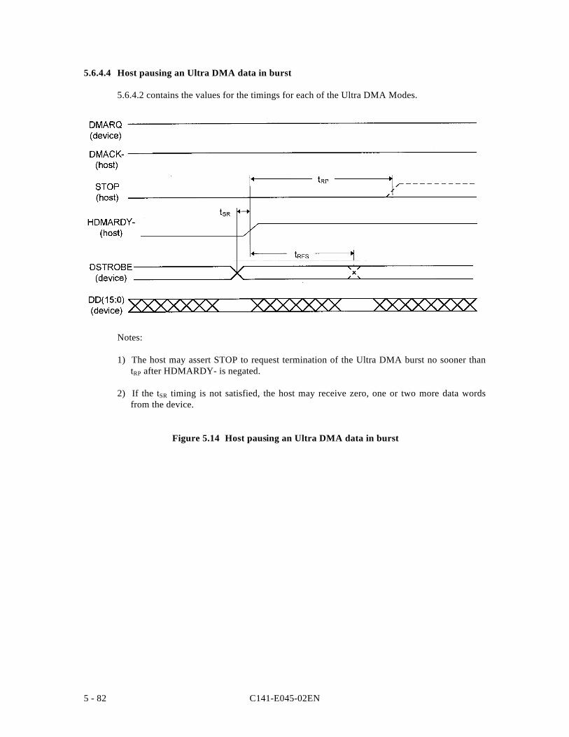
C141-E045-02EN5 - 82
5.6.4.4 Host pausing an Ultra DMA data in burst
5.6.4.2 contains the values for the timings for each of the Ultra DMA Modes.
Notes:
1) The host may assert STOP to request termination of the Ultra DMA burst no sooner thantRP after HDMARDY- is negated.
2) If the tSR timing is not satisfied, the host may receive zero, one or two more data wordsfrom the device.
Figure 5.14 Host pausing an Ultra DMA data in burst
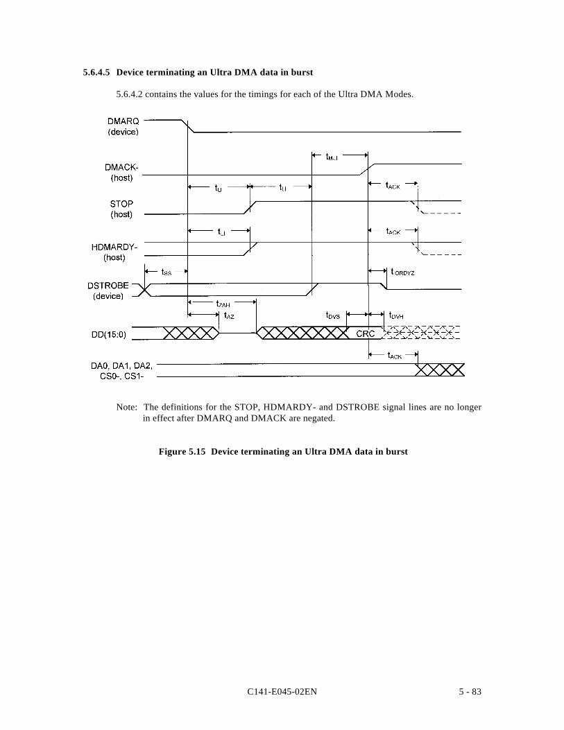
C141-E045-02EN 5 - 83
5.6.4.5 Device terminating an Ultra DMA data in burst
5.6.4.2 contains the values for the timings for each of the Ultra DMA Modes.
Note: The definitions for the STOP, HDMARDY- and DSTROBE signal lines are no longerin effect after DMARQ and DMACK are negated.
Figure 5.15 Device terminating an Ultra DMA data in burst
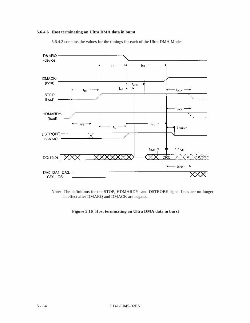
C141-E045-02EN5 - 84
5.6.4.6 Host terminating an Ultra DMA data in burst
5.6.4.2 contains the values for the timings for each of the Ultra DMA Modes.
Note: The definitions for the STOP, HDMARDY- and DSTROBE signal lines are no longerin effect after DMARQ and DMACK are negated.
Figure 5.16 Host terminating an Ultra DMA data in burst
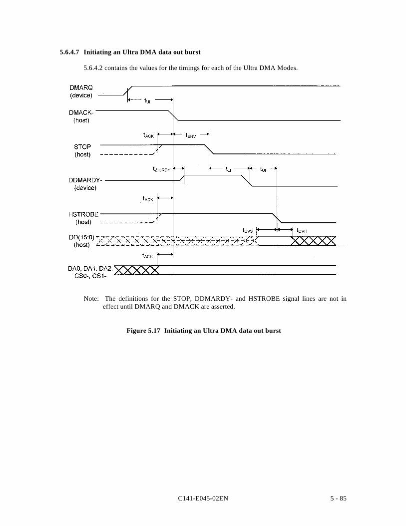
C141-E045-02EN 5 - 85
5.6.4.7 Initiating an Ultra DMA data out burst
5.6.4.2 contains the values for the timings for each of the Ultra DMA Modes.
Note: The definitions for the STOP, DDMARDY- and HSTROBE signal lines are not ineffect until DMARQ and DMACK are asserted.
Figure 5.17 Initiating an Ultra DMA data out burst
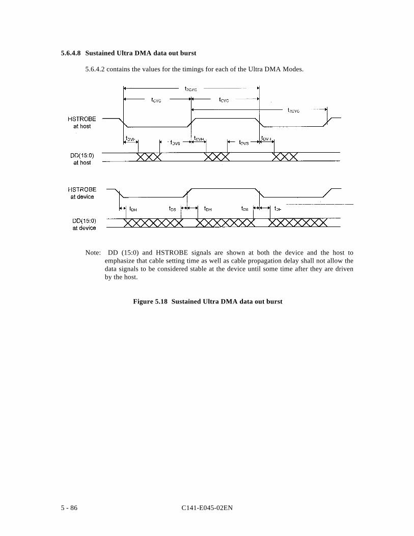
C141-E045-02EN5 - 86
5.6.4.8 Sustained Ultra DMA data out burst
5.6.4.2 contains the values for the timings for each of the Ultra DMA Modes.
Note: DD (15:0) and HSTROBE signals are shown at both the device and the host toemphasize that cable setting time as well as cable propagation delay shall not allow thedata signals to be considered stable at the device until some time after they are drivenby the host.
Figure 5.18 Sustained Ultra DMA data out burst
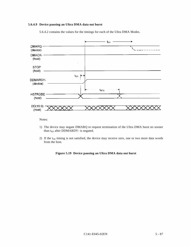
C141-E045-02EN 5 - 87
5.6.4.9 Device pausing an Ultra DMA data out burst
5.6.4.2 contains the values for the timings for each of the Ultra DMA Modes.
Notes:
1) The device may negate DMARQ to request termination of the Ultra DMA burst no soonerthan tRP after DDMARDY- is negated.
2) If the tSR timing is not satisfied, the device may receive zero, one or two more data wordsfrom the host.
Figure 5.19 Device pausing an Ultra DMA data out burst
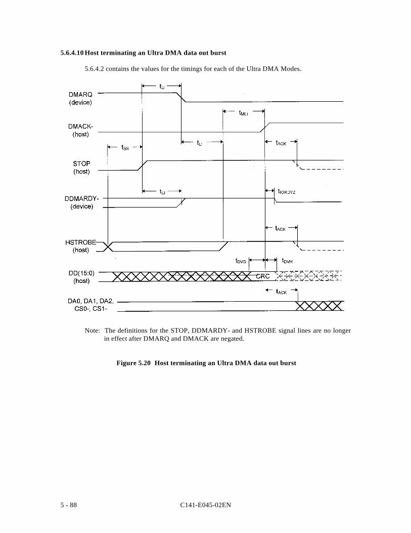
C141-E045-02EN5 - 88
5.6.4.10 Host terminating an Ultra DMA data out burst
5.6.4.2 contains the values for the timings for each of the Ultra DMA Modes.
Note: The definitions for the STOP, DDMARDY- and HSTROBE signal lines are no longerin effect after DMARQ and DMACK are negated.
Figure 5.20 Host terminating an Ultra DMA data out burst
C141-E045-02EN 5 - 89
5.6.4.11 Device terminating an Ultra DMA data in burst
5.6.4.2 contains the values for the timings for each of the Ultra DMA Modes.
Note: The definitions for the STOP, DDMARDY- and HSTROBE signal lines are no longerin effect after DMARQ and DMACK are negated.
Figure 5.21 Device terminating an Ultra DMA data out burst
C141-E045-02EN5 - 90
5.6.5 Power-on and reset
Figure 5.22 shows power-on and reset (hardware and software reset) timing.
(1) Only master device is present
*1: Reset means including Power-on-Reset, Hardware Reset (RESET-), and Software Reset.
Clear Reset *1
tP
tN
tM
BSY
DASP-
Power-onRESET-Software reset
(2) Master and slave devices are present (2-drives configuration)
tP
Clear Reset
[Slave device]
[Master device] tN
DASP-
PDIAG-
BSY
BSY
DASP-
tQ
tR
tS
Symbol Timing parameter Min. Max. Unit
tM Pulse width of RESET- 25 — µs
tN Time from RESET- negation to BSY set — 400 ns
tP Time from RESET- negation to DASP- or DIAG- negation — 1 ms
tQ Self-diagnostics execution time — 30 s
tR Time from RESET- negation to DASP- assertion (slave device) — 400 ms
tS Duration of DASP- assertion — 31 s
Figure 5.22 Power-on Reset Timing
C141-E045-02EN 6 - 1
CHAPTER 6 OPERATIONS
6.1 Device Response to the Reset
6.2 Address Translation
6.3 Power Save
6.4 Defect Management
6.5 Read-Ahead Cache
6.6 Write Cache
6.1 Device Response to the Reset
This section describes how the PDIAG- and DASP- signals responds when the power of theIDD is turned on or the IDD receives a reset or diagnostic command.
C141-E045-02EN6 - 2
6.1.1 Response to power-on
After the master device (device 0) releases its own power-on reset state, the master deviceshall check a DASP- signal for up to 450 ms to confirm presence of a slave device (device 1).The master device recognizes presence of the slave device when it confirms assertion of theDASP- signal. Then, the master device checks a PDIAG- signal to see if the slave device hassuccessfully completed the power-on diagnostics.
If the master device cannot confirm assertion of the DASP- signal within 450 ms, the masterdevice recognizes that no slave device is connected.
After the slave device (device 1) releases its own power-on reset state, the slave device shallreport its presence and the result of power-on diagnostics to the master device as describedbelow:
DASP- signal: Asserted within 400 ms.PDIAG- signal: Negated within 1 ms and asserted within 30 seconds.
Max. 400 ms.
Max. 30 sec.
Max. 1 ms.
If presence of a slave device isconfirmed, PDIAG- is checked forup to 31 seconds.
Checks DASP- for up to450 ms.
Max. 31 sec.
DASP-
PDIAG-
BSY bit
Power On Reset-
Status Reg.BSY bit
Power On Reset-
Slave device
Master device
Power on
Figure 6.1 Response to power-on
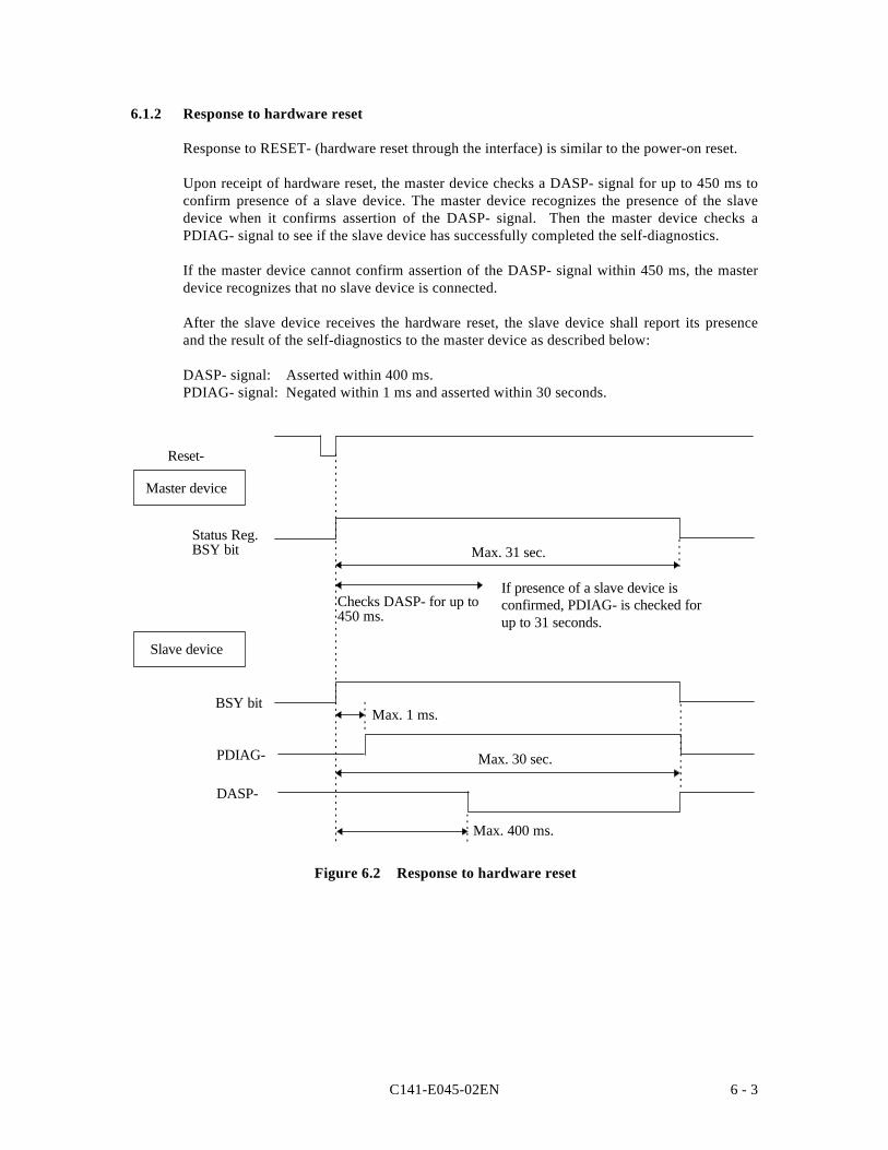
C141-E045-02EN 6 - 3
6.1.2 Response to hardware reset
Response to RESET- (hardware reset through the interface) is similar to the power-on reset.
Upon receipt of hardware reset, the master device checks a DASP- signal for up to 450 ms toconfirm presence of a slave device. The master device recognizes the presence of the slavedevice when it confirms assertion of the DASP- signal. Then the master device checks aPDIAG- signal to see if the slave device has successfully completed the self-diagnostics.
If the master device cannot confirm assertion of the DASP- signal within 450 ms, the masterdevice recognizes that no slave device is connected.
After the slave device receives the hardware reset, the slave device shall report its presenceand the result of the self-diagnostics to the master device as described below:
DASP- signal: Asserted within 400 ms.PDIAG- signal: Negated within 1 ms and asserted within 30 seconds.
Max. 31 sec.
Max. 400 ms.
Max. 30 sec.
Max. 1 ms.
If presence of a slave device isconfirmed, PDIAG- is checked forup to 31 seconds.
Checks DASP- for up to450 ms.
DASP-
PDIAG-
BSY bit
Reset-
Status Reg.BSY bit
Slave device
Master device
Figure 6.2 Response to hardware reset
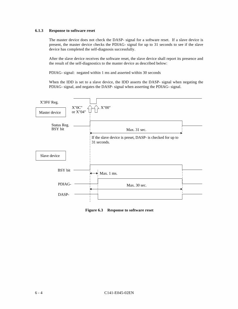
C141-E045-02EN6 - 4
6.1.3 Response to software reset
The master device does not check the DASP- signal for a software reset. If a slave device ispresent, the master device checks the PDIAG- signal for up to 31 seconds to see if the slavedevice has completed the self-diagnosis successfully.
After the slave device receives the software reset, the slave device shall report its presence andthe result of the self-diagnostics to the master device as described below:
PDIAG- signal: negated within 1 ms and asserted within 30 seconds
When the IDD is set to a slave device, the IDD asserts the DASP- signal when negating thePDIAG- signal, and negates the DASP- signal when asserting the PDIAG- signal.
Max. 31 sec.
Max. 30 sec.
Max. 1 ms.
If the slave device is preset, DASP- is checked for up to31 seconds.
DASP-
PDIAG-
BSY bit
X"00"X'3F6' Reg.
X"0C"or X"04"
Status Reg.BSY bit
Slave device
Master device
Figure 6.3 Response to software reset
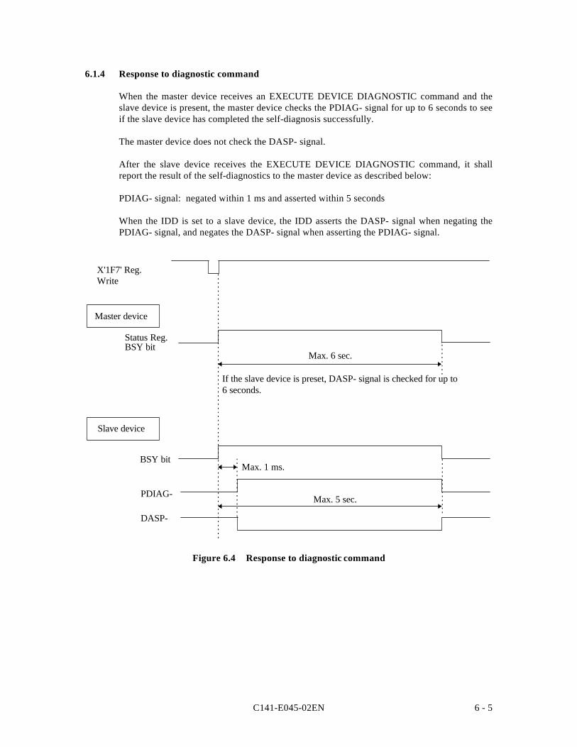
C141-E045-02EN 6 - 5
6.1.4 Response to diagnostic command
When the master device receives an EXECUTE DEVICE DIAGNOSTIC command and theslave device is present, the master device checks the PDIAG- signal for up to 6 seconds to seeif the slave device has completed the self-diagnosis successfully.
The master device does not check the DASP- signal.
After the slave device receives the EXECUTE DEVICE DIAGNOSTIC command, it shallreport the result of the self-diagnostics to the master device as described below:
PDIAG- signal: negated within 1 ms and asserted within 5 seconds
When the IDD is set to a slave device, the IDD asserts the DASP- signal when negating thePDIAG- signal, and negates the DASP- signal when asserting the PDIAG- signal.
Max. 6 sec.
Max. 5 sec.
Max. 1 ms.
If the slave device is preset, DASP- signal is checked for up to6 seconds.
DASP-
PDIAG-
BSY bit
X'1F7' Reg.Write
Status Reg.BSY bit
Slave device
Master device
Figure 6.4 Response to diagnostic command
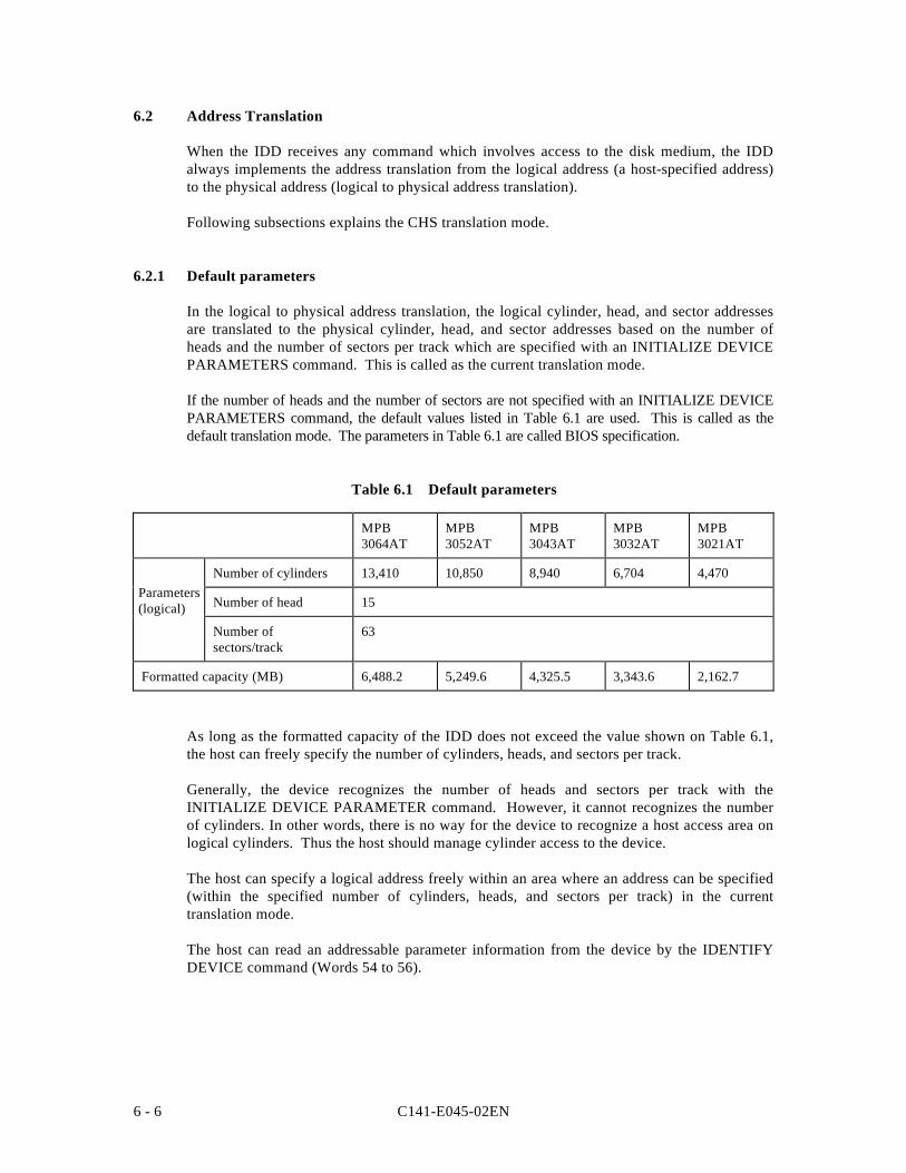
C141-E045-02EN6 - 6
6.2 Address Translation
When the IDD receives any command which involves access to the disk medium, the IDDalways implements the address translation from the logical address (a host-specified address)to the physical address (logical to physical address translation).
Following subsections explains the CHS translation mode.
6.2.1 Default parameters
In the logical to physical address translation, the logical cylinder, head, and sector addressesare translated to the physical cylinder, head, and sector addresses based on the number ofheads and the number of sectors per track which are specified with an INITIALIZE DEVICEPARAMETERS command. This is called as the current translation mode.
If the number of heads and the number of sectors are not specified with an INITIALIZE DEVICEPARAMETERS command, the default values listed in Table 6.1 are used. This is called as thedefault translation mode. The parameters in Table 6.1 are called BIOS specification.
Table 6.1 Default parameters
MPB3064AT
MPB3052AT
MPB3043AT
MPB3032AT
MPB3021AT
Number of cylinders 13,410 10,850 8,940 6,704 4,470
Number of head 15
Number ofsectors/track
63
Formatted capacity (MB) 6,488.2 5,249.6 4,325.5 3,343.6 2,162.7
As long as the formatted capacity of the IDD does not exceed the value shown on Table 6.1,the host can freely specify the number of cylinders, heads, and sectors per track.
Generally, the device recognizes the number of heads and sectors per track with theINITIALIZE DEVICE PARAMETER command. However, it cannot recognizes the numberof cylinders. In other words, there is no way for the device to recognize a host access area onlogical cylinders. Thus the host should manage cylinder access to the device.
The host can specify a logical address freely within an area where an address can be specified(within the specified number of cylinders, heads, and sectors per track) in the currenttranslation mode.
The host can read an addressable parameter information from the device by the IDENTIFYDEVICE command (Words 54 to 56).
Parameters(logical)
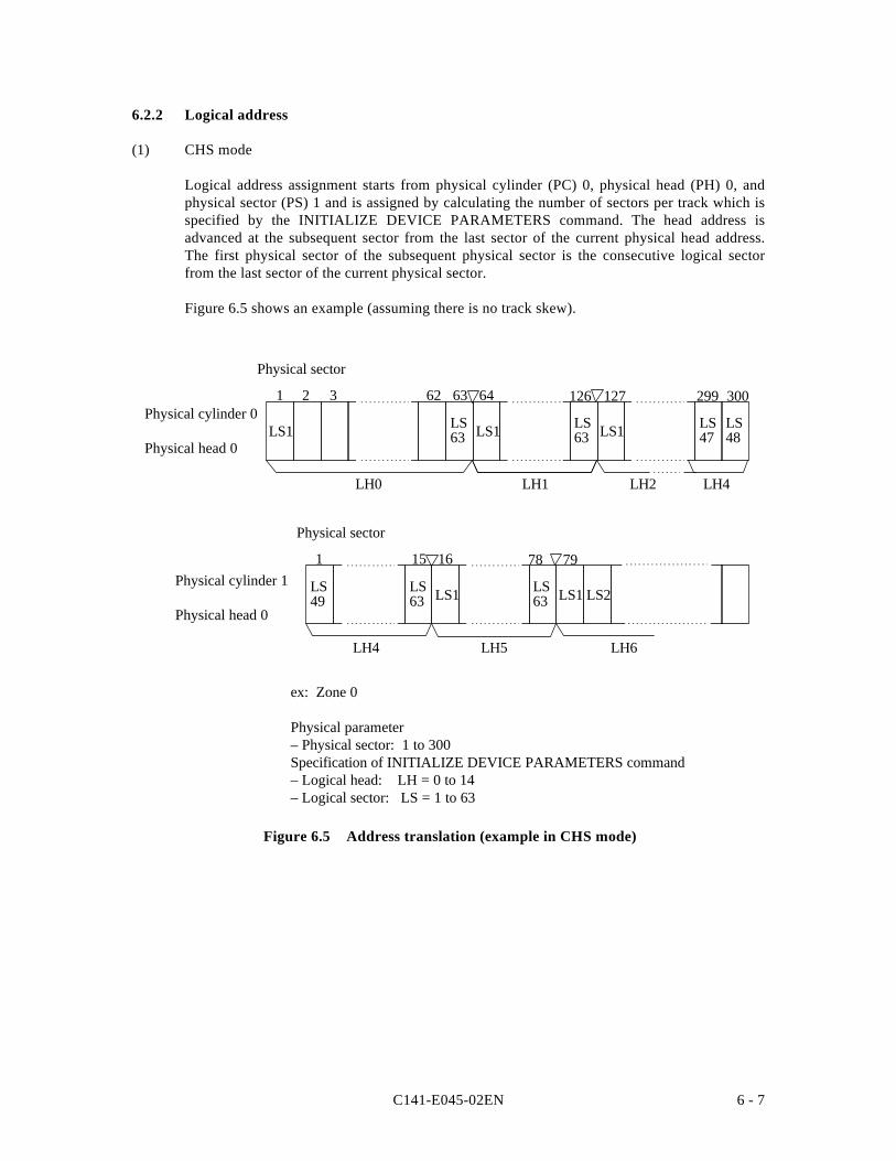
C141-E045-02EN 6 - 7
6.2.2 Logical address
(1) CHS mode
Logical address assignment starts from physical cylinder (PC) 0, physical head (PH) 0, andphysical sector (PS) 1 and is assigned by calculating the number of sectors per track which isspecified by the INITIALIZE DEVICE PARAMETERS command. The head address isadvanced at the subsequent sector from the last sector of the current physical head address.The first physical sector of the subsequent physical sector is the consecutive logical sectorfrom the last sector of the current physical sector.
Figure 6.5 shows an example (assuming there is no track skew).
1271266462 6332
LS1LS63
LH4LH2LH1LH0
LS1
1
Physical sector
Physical head 0
ex: Zone 0
Physical parameter– Physical sector: 1 to 300Specification of INITIALIZE DEVICE PARAMETERS command– Logical head: LH = 0 to 14– Logical sector: LS = 1 to 63
Physical cylinder 0300299
LS1 LS48
LS47
LS63
79781615
LS1LS49
LS63
LH6LH5LH4
1
Physical sector
LS2LS1LS63
Physical head 0
Physical cylinder 1
Figure 6.5 Address translation (example in CHS mode)
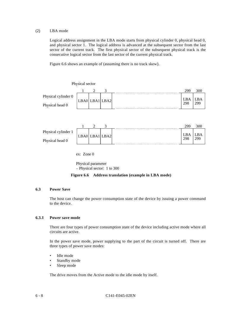
C141-E045-02EN6 - 8
(2) LBA mode
Logical address assignment in the LBA mode starts from physical cylinder 0, physical head 0,and physical sector 1. The logical address is advanced at the subsequent sector from the lastsector of the current track. The first physical sector of the subsequent physical track is theconsecutive logical sector from the last sector of the current physical track.
Figure 6.6 shows an example of (assuming there is no track skew).
Physical head 0
Physical cylinder 0LBA298LBA2LBA1LBA0
300299321
LBA299
Physical sector
ex: Zone 0
Physical parameter– Physical sector: 1 to 300
LBA298LBA2LBA1LBA0
300299321
LBA299Physical head 0
Physical cylinder 1
Figure 6.6 Address translation (example in LBA mode)
6.3 Power Save
The host can change the power consumption state of the device by issuing a power commandto the device.
6.3.1 Power save mode
There are four types of power consumption state of the device including active mode where allcircuits are active.
In the power save mode, power supplying to the part of the circuit is turned off. There arethree types of power save modes:
• Idle mode• Standby mode• Sleep mode
The drive moves from the Active mode to the idle mode by itself.
C141-E045-02EN 6 - 9
Regardless of whether the power down is enabled, the device enters the idle mode. The devicealso enters the idle mode in the same way after power-on sequence is completed.
(1) Active mode
In this mode, all the electric circuit in the device are active or the device is under seek, read orwrite operation.
A device enters the active mode under the following conditions:
• Power-on sequence is completed.
• A command other than power commands is issued.
• Reset (hardware or software)
(2) Idle mode
In this mode, circuits on the device is set to power save mode.
The device enters the Idle mode under the following conditions:
• After completion of power-on sequence.
• After completion of the command execution other than SLEEP and STANDBYcommands.
• Reset (hardware or software)
(3) Standby mode
In this mode, the VCM circuit is turned off and the spindle motor is stopped.
The device can receive commands through the interface. However if a command with diskaccess is issued, response time to the command under the standby mode takes longer than theactive or Idle mode because the access to the disk medium cannot be made immediately.
The drive enters the standby mode under the following conditions:
• A STANDBY or STANDBY IMMEDIATE command is issued in the active or idle mode.
• When automatic power down sequence is enabled, the timer has elapsed.
• A reset is issued in the sleep mode.
When one of following commands is issued, the command is executed normally and thedevice is still stayed in the standby mode.
• Reset (hardware or software)
C141-E045-02EN6 - 10
• STANDBY command
• STANDBY IMMEDIATE command
• INITIALIZE DEVICE PARAMETERS command
• CHECK POWER MODE command
(4) Sleep mode
The power consumption of the drive is minimal in this mode. The drive enters only thestandby mode from the sleep mode. The only method to return from the standby mode is toexecute a software or hardware reset.
The drive enters the sleep mode under the following condition:
• A SLEEP command is issued.
Issued commands are invalid (ignored) in this mode.
6.3.2 Power commands
The following commands are available as power commands.
• IDLE
• IDLE IMMEDIATE
• STANDBY
• STANDBY IMMEDIATE
• SLEEP
• CHECK POWER MODE
6.4 Defect Management
Defective sectors of which the medium defect location is registered in the system space arereplaced with spare sectors in the formatting at the factory shipment.
All the user space area are formatted at shipment from the factory based on the defaultparameters listed in Table 6.1.
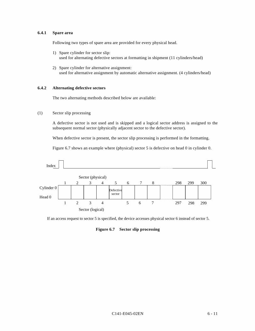
C141-E045-02EN 6 - 11
6.4.1 Spare area
Following two types of spare area are provided for every physical head.
1) Spare cylinder for sector slip:used for alternating defective sectors at formatting in shipment (11 cylinders/head)
2) Spare cylinder for alternative assignment:used for alternative assignment by automatic alternative assignment. (4 cylinders/head)
6.4.2 Alternating defective sectors
The two alternating methods described below are available:
(1) Sector slip processing
A defective sector is not used and is skipped and a logical sector address is assigned to thesubsequent normal sector (physically adjacent sector to the defective sector).
When defective sector is present, the sector slip processing is performed in the formatting.
Figure 6.7 shows an example where (physical) sector 5 is defective on head 0 in cylinder 0.
21
Index
Head 0
Defectivesector
If an access request to sector 5 is specified, the device accesses physical sector 6 instead of sector 5.
Sector (logical)
Sector (physical)
Cylinder 043 65
297
30029929887
21 43 65 7 299298
Figure 6.7 Sector slip processing
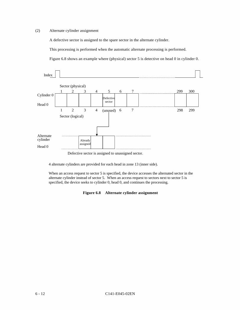
C141-E045-02EN6 - 12
(2) Alternate cylinder assignment
A defective sector is assigned to the spare sector in the alternate cylinder.
This processing is performed when the automatic alternate processing is performed.
Figure 6.8 shows an example where (physical) sector 5 is detective on head 0 in cylinder 0.
5 76431 3002992
Index
Cylinder 0
Head 0
Head 0
Alreadyassigned
Defectivesector
4 alternate cylinders are provided for each head in zone 13 (inner side).
When an access request to sector 5 is specified, the device accesses the alternated sector in thealternate cylinder instead of sector 5. When an access request to sectors next to sector 5 isspecified, the device seeks to cylinder 0, head 0, and continues the processing.
Defective sector is assigned to unassigned sector.
(unused)Sector (logical)
Sector (physical)
Alternatecylinder
21 43 6 7 299298
Figure 6.8 Alternate cylinder assignment
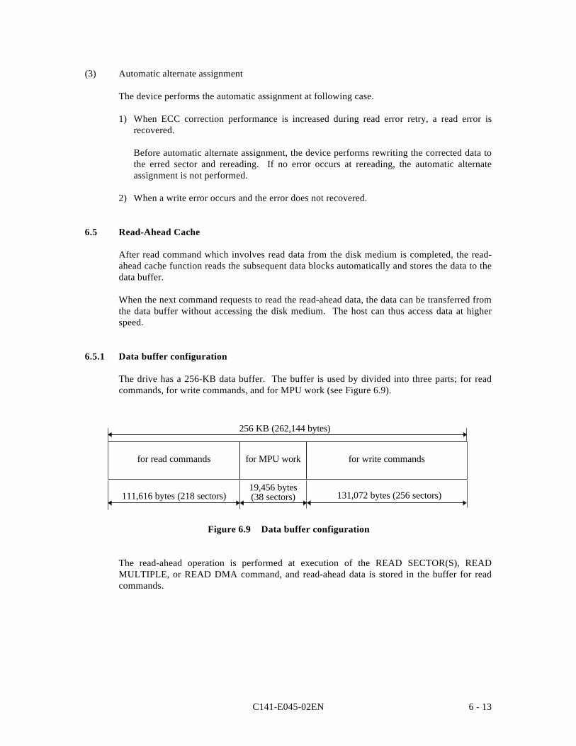
C141-E045-02EN 6 - 13
(3) Automatic alternate assignment
The device performs the automatic assignment at following case.
1) When ECC correction performance is increased during read error retry, a read error isrecovered.
Before automatic alternate assignment, the device performs rewriting the corrected data tothe erred sector and rereading. If no error occurs at rereading, the automatic alternateassignment is not performed.
2) When a write error occurs and the error does not recovered.
6.5 Read-Ahead Cache
After read command which involves read data from the disk medium is completed, the read-ahead cache function reads the subsequent data blocks automatically and stores the data to thedata buffer.
When the next command requests to read the read-ahead data, the data can be transferred fromthe data buffer without accessing the disk medium. The host can thus access data at higherspeed.
6.5.1 Data buffer configuration
The drive has a 256-KB data buffer. The buffer is used by divided into three parts; for readcommands, for write commands, and for MPU work (see Figure 6.9).
256 KB (262,144 bytes)
for write commandsfor MPU work
19,456 bytes(38 sectors)111,616 bytes (218 sectors) 131,072 bytes (256 sectors)
for read commands
Figure 6.9 Data buffer configuration
The read-ahead operation is performed at execution of the READ SECTOR(S), READMULTIPLE, or READ DMA command, and read-ahead data is stored in the buffer for readcommands.
C141-E045-02EN6 - 14
6.5.2 Caching operation
Caching operation is performed only at issuance of the following commands. The devicetransfers data from the data buffer to the host system at issuance of following command iffollowing data exist in the data buffer.
• All sectors to be processed by the command• A part of data including load sector to be processed by the command
When a part of data to be processed exist in the data buffer, remaining data are read from themedium and are transferred to the host system.
(1) Commands that are object of caching operation
Follow commands are object of caching operation.
• READ SECTOR (S)• READ MULTIPLE• READ DMA
When caching operation is disabled by the SET FEATURES command, no caching operationis performed.
(2) Data that are object of caching operation
Follow data are object of caching operation.
1) Read-ahead data read from the medium to the data buffer after completion of the commandthat are object of caching operation.
2) Data transferred to the host system once by requesting with the command that are object ofcaching operation (except for the cache invalid data by some reasons).
3) Remaining data in the data buffer (for write command) transferred from the host system bythe command that writes data onto the disk medium, such as the WRITE SECTOR (S),WRITE DMA, WRITE MULTIPLE.
Followings are definition of in case that the write data is treated as a cache data. However,since the hit check at issuance of read command is performed to the data buffer for readcommand priority, caching write data is limited to the case that the hit check is missed at thedata buffer for read command.
• When all data requested by the read command are stored in the data buffer for writecommand (hit all), the device transfers data from the data buffer for write command. Atthis time, the read-ahead operation to the data subsequent to the requested data is notperformed.
• Even if a part of data requested by the read command are stored in the data buffer forwrite command (hit partially), all data are read from the disk medium without transferringfrom the data buffer for write command.
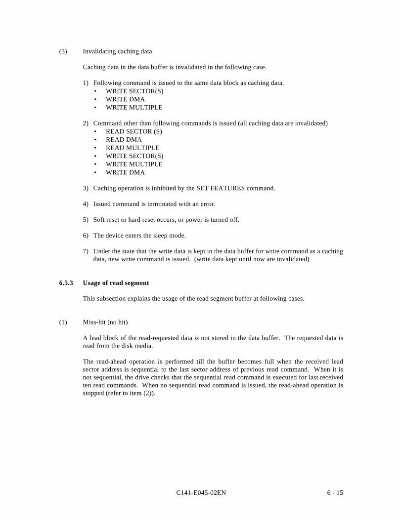
C141-E045-02EN 6 - 15
(3) Invalidating caching data
Caching data in the data buffer is invalidated in the following case.
1) Following command is issued to the same data block as caching data.• WRITE SECTOR(S)• WRITE DMA• WRITE MULTIPLE
2) Command other than following commands is issued (all caching data are invalidated)• READ SECTOR (S)• READ DMA• READ MULTIPLE• WRITE SECTOR(S)• WRITE MULTIPLE• WRITE DMA
3) Caching operation is inhibited by the SET FEATURES command.
4) Issued command is terminated with an error.
5) Soft reset or hard reset occurs, or power is turned off.
6) The device enters the sleep mode.
7) Under the state that the write data is kept in the data buffer for write command as a cachingdata, new write command is issued. (write data kept until now are invalidated)
6.5.3 Usage of read segment
This subsection explains the usage of the read segment buffer at following cases.
(1) Miss-hit (no hit)
A lead block of the read-requested data is not stored in the data buffer. The requested data isread from the disk media.
The read-ahead operation is performed till the buffer becomes full when the received leadsector address is sequential to the last sector address of previous read command. When it isnot sequential, the drive checks that the sequential read command is executed for last receivedten read commands. When no sequential read command is issued, the read-ahead operation isstopped (refer to item (2)).
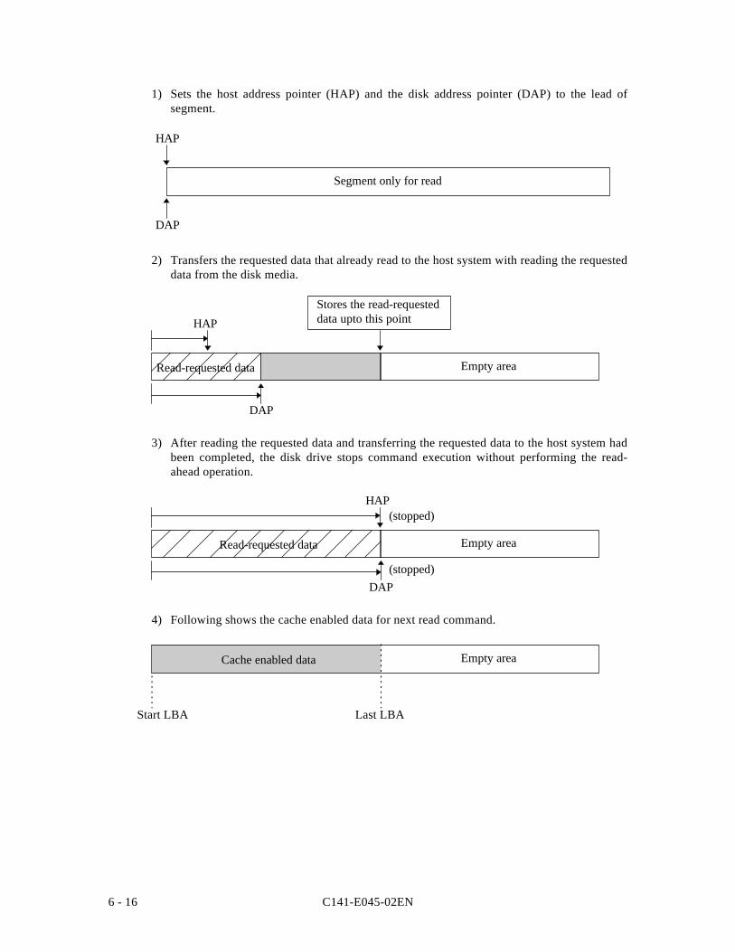
C141-E045-02EN6 - 16
1) Sets the host address pointer (HAP) and the disk address pointer (DAP) to the lead ofsegment.
Segment only for read
DAP
HAP
2) Transfers the requested data that already read to the host system with reading the requesteddata from the disk media.
Read-requested data
Stores the read-requesteddata upto this point
Empty area
DAP
HAP
3) After reading the requested data and transferring the requested data to the host system hadbeen completed, the disk drive stops command execution without performing the read-ahead operation.
Read-requested data Empty area
DAP(stopped)
(stopped)HAP
4) Following shows the cache enabled data for next read command.
Cache enabled data Empty area
Last LBAStart LBA
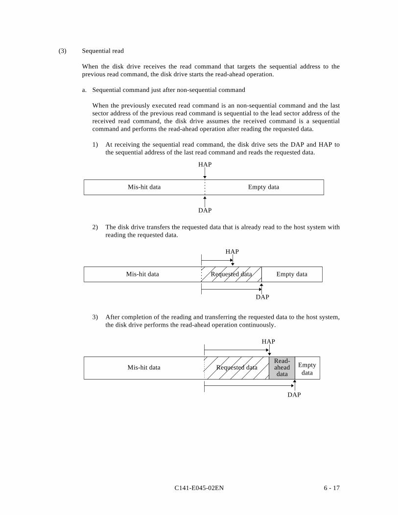
C141-E045-02EN 6 - 17
(3) Sequential read
When the disk drive receives the read command that targets the sequential address to theprevious read command, the disk drive starts the read-ahead operation.
a. Sequential command just after non-sequential command
When the previously executed read command is an non-sequential command and the lastsector address of the previous read command is sequential to the lead sector address of thereceived read command, the disk drive assumes the received command is a sequentialcommand and performs the read-ahead operation after reading the requested data.
1) At receiving the sequential read command, the disk drive sets the DAP and HAP tothe sequential address of the last read command and reads the requested data.
Empty dataMis-hit data
2) The disk drive transfers the requested data that is already read to the host system withreading the requested data.
Requested data
DAP
HAP
Mis-hit data Empty data
3) After completion of the reading and transferring the requested data to the host system,the disk drive performs the read-ahead operation continuously.
Mis-hit data Requested data
DAP
HAP
Emptydata
Read-aheaddata
DAP
HAP
C141-E045-02EN6 - 18
4) The disk drive performs the read-ahead operation for all area of segment withoverwriting the requested data. Finally, the cache data in the buffer is as follows.
Start LBALast LBA
DAP
HAP
Read-ahead data
b. Sequential hit
When the previously executed read command is the sequential command and the lastsector address of the previous read command is sequential to the lead sector address of thereceived read command, the disk drive transfers the hit data in the buffer to the hostsystem.
The disk drive performs the read-ahead operation of the new continuous data to the emptyarea that becomes vacant by data transfer at the same time as the disk drive startstransferring data to the host system.
1) In the case that the contents of buffer is as follows at receiving a read command;
Start LBALast LBADAP
HAP (Completion of transferring requested data)
Hit dataRead-ahead data
2) The disk drive starts the read-ahead operation to the empty area that becomes vacantby data transfer at the same time as the disk drive starts transferring hit data.
DAP
HAP
Hit dataNew read-ahead dataRead-ahead data
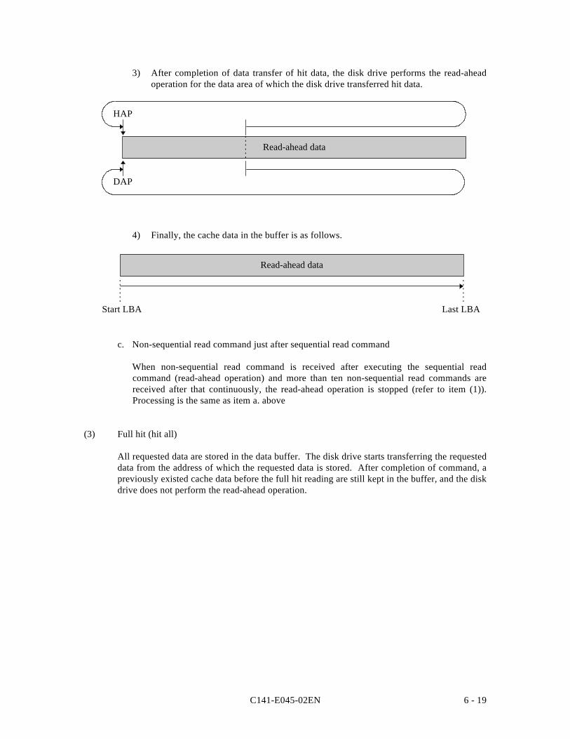
C141-E045-02EN 6 - 19
3) After completion of data transfer of hit data, the disk drive performs the read-aheadoperation for the data area of which the disk drive transferred hit data.
Read-ahead data
4) Finally, the cache data in the buffer is as follows.
Read-ahead data
c. Non-sequential read command just after sequential read command
When non-sequential read command is received after executing the sequential readcommand (read-ahead operation) and more than ten non-sequential read commands arereceived after that continuously, the read-ahead operation is stopped (refer to item (1)).Processing is the same as item a. above
(3) Full hit (hit all)
All requested data are stored in the data buffer. The disk drive starts transferring the requesteddata from the address of which the requested data is stored. After completion of command, apreviously existed cache data before the full hit reading are still kept in the buffer, and the diskdrive does not perform the read-ahead operation.
Last LBAStart LBA
DAP
HAP
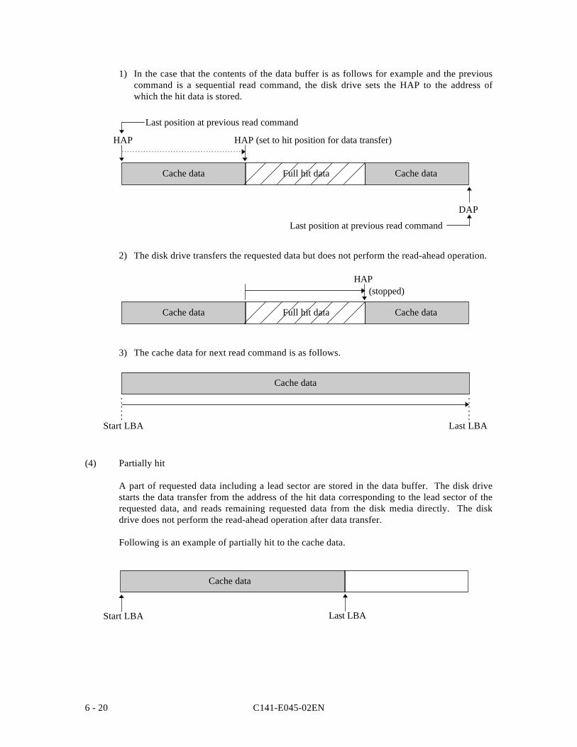
C141-E045-02EN6 - 20
1) In the case that the contents of the data buffer is as follows for example and the previouscommand is a sequential read command, the disk drive sets the HAP to the address ofwhich the hit data is stored.
HAP (set to hit position for data transfer)
Last position at previous read command
Last position at previous read command
Cache dataFull hit dataCache data
2) The disk drive transfers the requested data but does not perform the read-ahead operation.
(stopped)HAP
Cache dataFull hit dataCache data
3) The cache data for next read command is as follows.
Cache data
(4) Partially hit
A part of requested data including a lead sector are stored in the data buffer. The disk drivestarts the data transfer from the address of the hit data corresponding to the lead sector of therequested data, and reads remaining requested data from the disk media directly. The diskdrive does not perform the read-ahead operation after data transfer.
Following is an example of partially hit to the cache data.
Last LBA
Cache data
DAP
HAP
Last LBAStart LBA
Start LBA
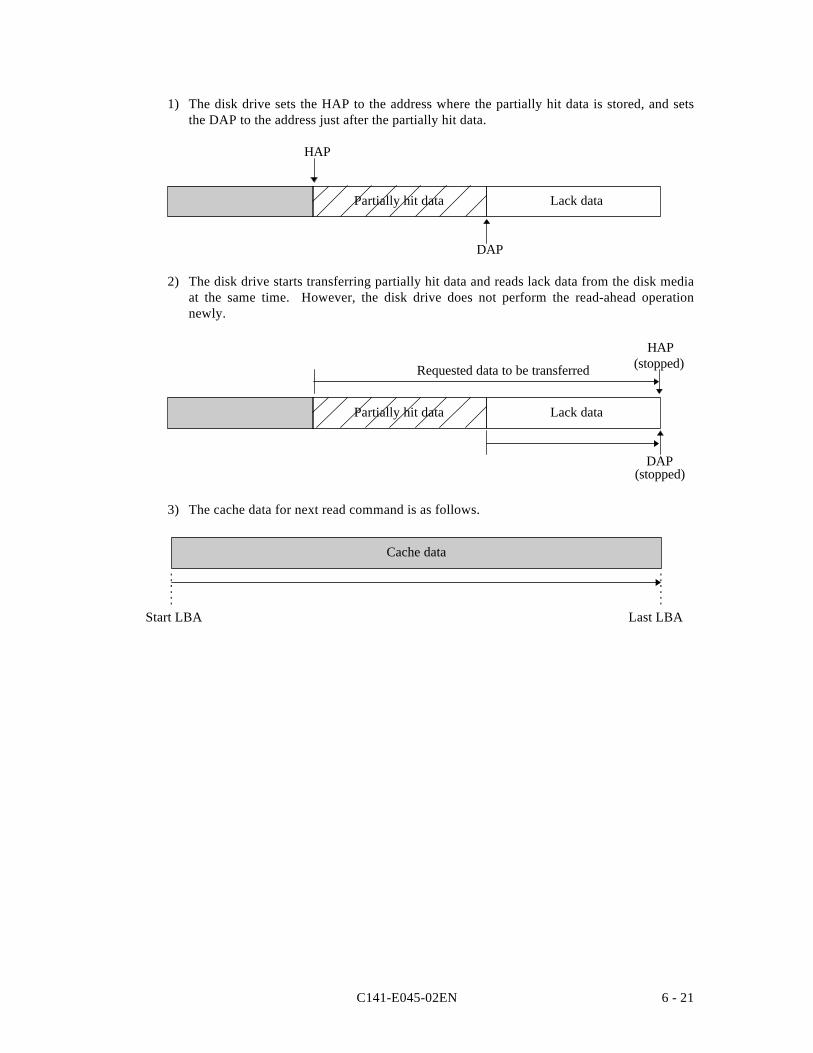
C141-E045-02EN 6 - 21
1) The disk drive sets the HAP to the address where the partially hit data is stored, and setsthe DAP to the address just after the partially hit data.
HAP
DAP
Partially hit data Lack data
2) The disk drive starts transferring partially hit data and reads lack data from the disk mediaat the same time. However, the disk drive does not perform the read-ahead operationnewly.
(stopped)HAP
(stopped)
Requested data to be transferred
DAP
Partially hit data Lack data
3) The cache data for next read command is as follows.
Cache data
Last LBAStart LBA
C141-E045-02EN6 - 22
6.6 Write Cache
The write cache function of the drive makes a high speed processing in the case that data to bewritten by a write command is logically sequent the data of previous command and randomwrite operation is performed.
When the drive receives a write command, the drive starts transferring data of sectorsrequested by the host system and writing on the disk medium. After transferring data ofsectors requested by the host system, the drive generates the interrupt of command complete.Also, the drive sets the normal end status in the Status register. The drive continues writingdata on the disk medium. When all data requested by the host are written on the disk medium,actual write operation is completed.
The drive receives the next command continuously. If the received command is a "sequentialwrite" (data to be written by a command is logically sequent to data of previous command),the drive starts data transfer and receives data of sectors requested by the host system. At thistime, if the write operation of the previous command is still been executed, the drivecontinuously executes the write operation of the next command from the sector next to the lastsector of the previous write operation. Thus, the latency time for detecting a target sector ofthe next command is eliminated. This shortens the access time. The drive generates aninterrupt of command complete after completion of data transfer requested by the host systemas same as at previous command. When the write operation of the previous command hadbeen completed, the latency time occurs to search the target sector.
If the received command is not a "sequential write", the drive receives data of sectorsrequested by the host system as same as "sequential write". The drive generates the interruptof command complete after completion of data transfer requested by the host system.Received data is processed after completion of the write operation to the disk medium of theprevious command.
Even if a hard reset or soft reset is received or the write cache function is disabled by the SETFEATURES command during unwritten data is kept, the instruction is not executed untilremaining unwritten data is written onto the disk medium.
The drive uses a write data as a read cache data. When a read command is issued to the sameaddress after the write command, the read operation to the disk medium is not performed.
When an error occurs during the write operation, the drive makes retry as much as possible. Ifthe error cannot be recovered by retry, the drive stops the write operation to the erred sector,and continues the write operation from the next sector if the write data is remained. (If thedrive stacks a write command, for that the drive posts the command completion, next to thecommand that write operation is stopped by error occurrence.) After an error occurs at abovewrite operation, the drive posts the error status to the host system at next command. (Thedrive does not execute this command, sets the error status that occurred at the write operation,and generates the interrupt for abnormal end. However, when the drive receives a writecommand after the completion of error processing, the drive posts the error after writing thewrite data of the write command.)
C141-E045-02EN 6 - 23
At the time that the drive has stopped the command execution after the error recovery hasfailed, the write cache function is disabled automatically. The releasing the disable state canbe done by the SET FEATURES command. When the power of the drive is turned on afterthe power is turned off once, the status of the write cache function returns to the default state.The default state is “write cache enable”, and can be disable by the SET FEATUREScommand.
The write cache function is operated with the following command.
• WRITE SECTOR(S)• WRITE MULTIPLE• WRITE DMA
IMPORTANT
When the write cache function is enabled, the transferred data fromthe host by the WRITE SECTOR(S) is not completely written on thedisk medium at the time that the interrupt of command complete isgenerated. When the unrecoverable error occurs during the writeoperation, the command execution is stopped. Then, when the drivereceives the next command, it generates an interrupt of abnormalend. However an interrupt of abnormal end is not generated whena write automatic assignment succeeds. However, since the hostmay issue several write commands before the drive generates aninterrupt of abnormal end, the host cannot recognize that theoccurred error is for which command generally. Therefore, it isvery hard to retry the unrecoverable write error for the host in thewrite cache operation generally. So, take care to use the writecache function.
FUJITSU LIMITEDBusiness PlanningSolid Square East Tower580 Horikawa-cho,Saiwai-ku, Kawasaki,210-0913, JapanTEL: 81-44-540-4056FAX: 81-44-540-4123
FUJITSU COMPUTER PRODUCTS OF AMERICA, INC.2904 Orchard Parkway, San Jose,California 95134-2009, U.S.A.TEL: 1-408-432-6333FAX: 1-408-432-3908
FUJITSU CANADA INC.2800 Matheson Blvd. East, Mississauga, Toronto,Ontario L4W 4X5, CANADATEL: 1-905-602-5454FAX: 1-905-602-5457
FUJITSU EUROPE LIMITED2, Longwalk Road, Stockley Park, Uxbridge,Middlesex UB11 1AB, ENGLANDTEL: 44-81-573-4444FAX: 44-81-573-2643
FUJITSU DEUTSCHLAND GmbHFrankfurter Ring 211, 80807 München, GERMANYTEL: 49-89-323780FAX: 49-89-32378100
FUJITSU NORDIC ABKung Hans Väg 12, S-192 68 Sollentura, SWEDENTEL: 46-8-626-6000FAX: 46-8-626-6711
FUJITSU ITALIA S.p.A.Via Nazario Sauro, 38 20099 Sesto S. Giovanni (MI), ITALYTEL: 39-2-26294-1FAX: 39-2-26294-201
FUJITSU FRANCE S.A.I, Place des Etas-Unis, SILIC 310,94588 Rungis Cedex, FRANCETEL: 33-1-41-80-38-80FAX: 33-1-41-80-38-66
FUJITSU ICL ESPAÑA S.A.Almagro 40, 28010 Madrid, SPAINTEL: 34-1-581-8100FAX: 34-1-581-8125
FUJITSU AUSTRALIA LIMITED2 Julius Avenue (Cnr Delhi Road) North Ryde N.S.W. 2113,AUSTRALIATEL: 61-2-9776-4555FAX: 61-2-9776-4556
FUJITSU HONG KONG LTD.Room 2521, Sun Hung Kai Centre, 30 Harbour Road, HONGHONGTEL: 852-2827-5780FAX: 852-2827-4724
FUJITSU KOREA LTD.9th Floor, Korean Reinsurance Building, 80, Susong-Dong,Chongro-Gu, Seoul Special City, Republic of KOREATEL: 82-2-739-3281FAX: 82-2-739-3294
FUJITSU COMPUTERS (SINGAPORE) PTE. LTD20 Science Park Road #03-01,TELETECH PARK SINGAPORE SCIENCE PARK II,Singapore 117674TEL: 65-777-6577FAX: 65-771-5499
FUJITSU TAIWAN LTD.8F, Hun Tai Center, 168-170, Tun Hwa North Road,1st Sec., Taipei, TAIWANTEL: 886-2-545-7700FAX: 886-2-717-4644
FUJITSU SYSTEMS BUSINESS (MALAYSIA) SDN. BHD.Fujitsu Plaza, 1A, Jalan Tandang 204, P.O. Box 636 Pejabat PosJalan Sultan46770 Petaling Jaya, Selangor Darul Ehsan, MalaysiaTEL: 60-3-793-3888FAX: 60-3-793-0888
FUJITSU SYSTEMS BUSINESS (THAILAND) LTD.12th F1., Olympia Thai Tower, 444 Rachadapisek Road,Samsennok, Huay Kwang, Bangkok 10320, ThailandTEL: 66-2-512-6066FAX: 66-2-512-6068
10
Comments concerning this manual can be directed to one of the following addresses:
Reader Comment FormWe would appreciate your comments and suggestions for improving this publication.
Publication No. Rev. Letter Title Current Date
How did you use this publication? Is the material presented effectively?
What is your overall rating of this publication? What is your occupation?
Your other comments may be entered here. Please be specific and give page,paragraph and line number references where applicable.
Your Name & Return Address
Sales
OperatingInstalling
Maintaining
Learning
Reference
Fair
Poor
Very Good
GoodVery Poor
Fullycovered
WellIllustrated
Thank you for your interest. Please send this sheet to one of the addresses in the left page.
WellOrganized
Clean
FUJITSU LIMITED