Embed Size (px)
Citation preview
C141-E038-02EN
MAA3182 SERIESMAB3045/MAB3091 SERIES
INTELLIGENT DISK DRIVES
SCSI PHYSICAL SPECIFICATIONS
C141-E038-02EN i
FOR SAFE OPERATION
Handling of This manual
This manual contains important information for using this product. Read thoroughly beforeusing the product. Use this product only after thoroughly reading and understandingespecially the section “Important Alert Items” in this manual. Keep this manual handy, andkeep it carefully.
FUJITSU makes every effort to prevent users and bystanders from being injured or fromsuffering damange to their property. Use the product according to this manual.
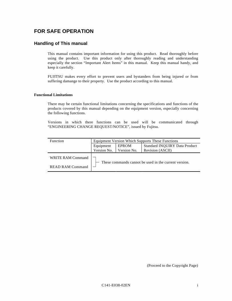
Functional Limitations
There may be certain functional limitations concerning the specifications and functions of theproducts covered by this manual depending on the equipment version, especially concerningthe following functions.
Versions in which there functions can be used will be communicated through“ENGINEERING CHANGE REQUEST/NOTICE”, issued by Fujitsu.
Function Equipment Version Which Supports These FunctionsEquipmentVersion No.
EPROMVersion No.
Standard INQUIRY Data ProductRevision (ASCII)
WRITE RAM Command These commands cannot be used in the current version.
READ RAM Command
(Proceed to the Copyright Page)
C141-E038-02ENii
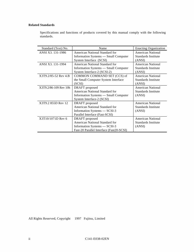
Related Standards
Specifications and functions of products covered by this manual comply with the followingstandards.
Standard (Text) No. Name Enacting OrganizationANSI X3. 131-1986 American National Standard for
Information Systems --- Small ComputerSystem Interface (SCSI)
American NationalStandards Institute(ANSI)
ANSI X3. 131-1994 American National Standard forInformation Systems --- Small ComputerSystem Interface-2 (SCSI-2)
American NationalStandards Institute(ANSI)
X3T9.2/85-52 Rev 4.B COMMON COMMAND SET (CCS) ofthe Small Computer System Interface(SCSI)
American NationalStandards Institute(ANSI)
X3T9.2/86-109 Rev 10h DRAFT proposedAmerican National Standard forInformation Systems --- Small ComputerSystem Interface-2 (SCSI)
American NationalStandards Institute(ANSI)
X3T9.2 855D Rev 12 DRAFT proposedAmerican National Standard forInformation Systems --- SCSI-3Parallel Interface (Fast-SCSI)
American NationalStandards Institute(ANSI)
X3T10/1071D Rev 6 DRAFT proposedAmerican National Standard forInformation Systems --- SCSI-3Fast-20 Parallel Interface (Fast20-SCSI)
American NationalStandards Institute(ANSI)
All Rights Reserved, Copyright 1997 Fujitsu, Limited
C141-E038-02EN iii
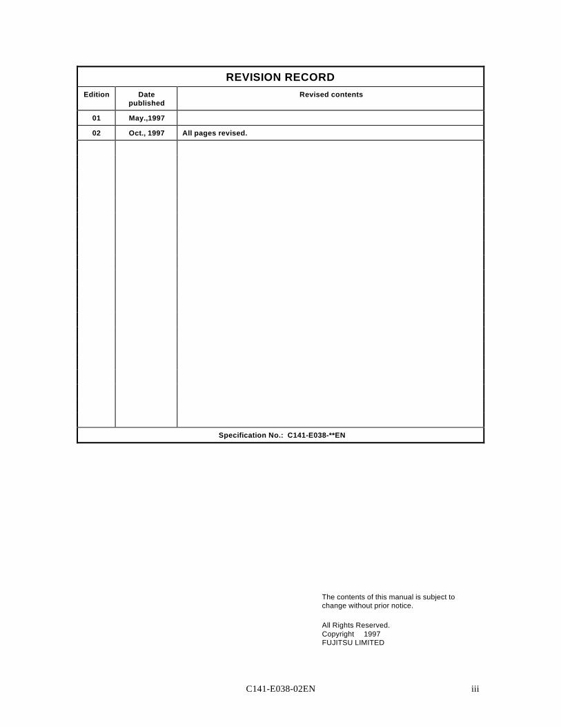
REVISION RECORDEdition Date
publishedRevised contents
01 May.,1997
02 Oct., 1997 All pages revised.
Specification No.: C141-E038-**EN
The contents of this manual is subject tochange without prior notice.
All Rights Reserved.Copyright 1997FUJITSU LIMITED


C141-E038-02EN v
PREFACE
This manual explains the MAA3182 and MAB3045/MAB3091 series 3-1/2" intelligent disk driveseach having the built-in SCSI controller.
This manual details the specifications and functions of the Small Computer System Interface (SCSI) toconnect the above listed disk drives to the user system. Also, the manual details various SCSIcommand specifications and the command processing functions, and provides the information requiredto creation of host system software. This manual is intended to be used by the users who have thebasic knowledge of computer system operations.
The following lists the manual configuration and the contents of each chapter. The caution labels andmarkings are also explained.
Manual Configuration and Contents
This manual consists of the following three chapters, and the terminologies and abbreviations sections.
Chapter 1 SCSI Bus
This chapter describes the configuration, physical and electrical requirements, interface protocol, andother operations of the Small Computer System Interface (SCSI) which connects the MAA3182 andMAB3045/MAB3091 series intelligent disk drives to the user system.
Chapter 2 SCSI Messages
This chapter describes the type and explanation of messages defined for SCSI bus operations.
Chapter 3 ERROR Recovery
This chapter describes error recovery processing executed by the MAA3182 and MAB3045/MAB3091series intelligent disk drives in response to various errors on the SCSI bus.
Glossary
This section explains the terminologies the reader must understand to read this manual.
Abbreviations
This section lists the abbreviated terms and their full words used in this manual.
C141-E038-02ENvi
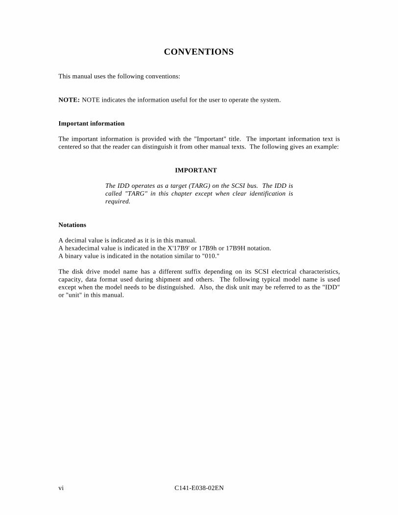
CONVENTIONS
This manual uses the following conventions:
NOTE: NOTE indicates the information useful for the user to operate the system.
Important information
The important information is provided with the "Important" title. The important information text iscentered so that the reader can distinguish it from other manual texts. The following gives an example:
IMPORTANT
The IDD operates as a target (TARG) on the SCSI bus. The IDD iscalled "TARG" in this chapter except when clear identification isrequired.
Notations
A decimal value is indicated as it is in this manual.A hexadecimal value is indicated in the X'17B9' or 17B9h or 17B9H notation.A binary value is indicated in the notation similar to "010."
The disk drive model name has a different suffix depending on its SCSI electrical characteristics,capacity, data format used during shipment and others. The following typical model name is usedexcept when the model needs to be distinguished. Also, the disk unit may be referred to as the "IDD"or "unit" in this manual.
C141-E038-02EN vii
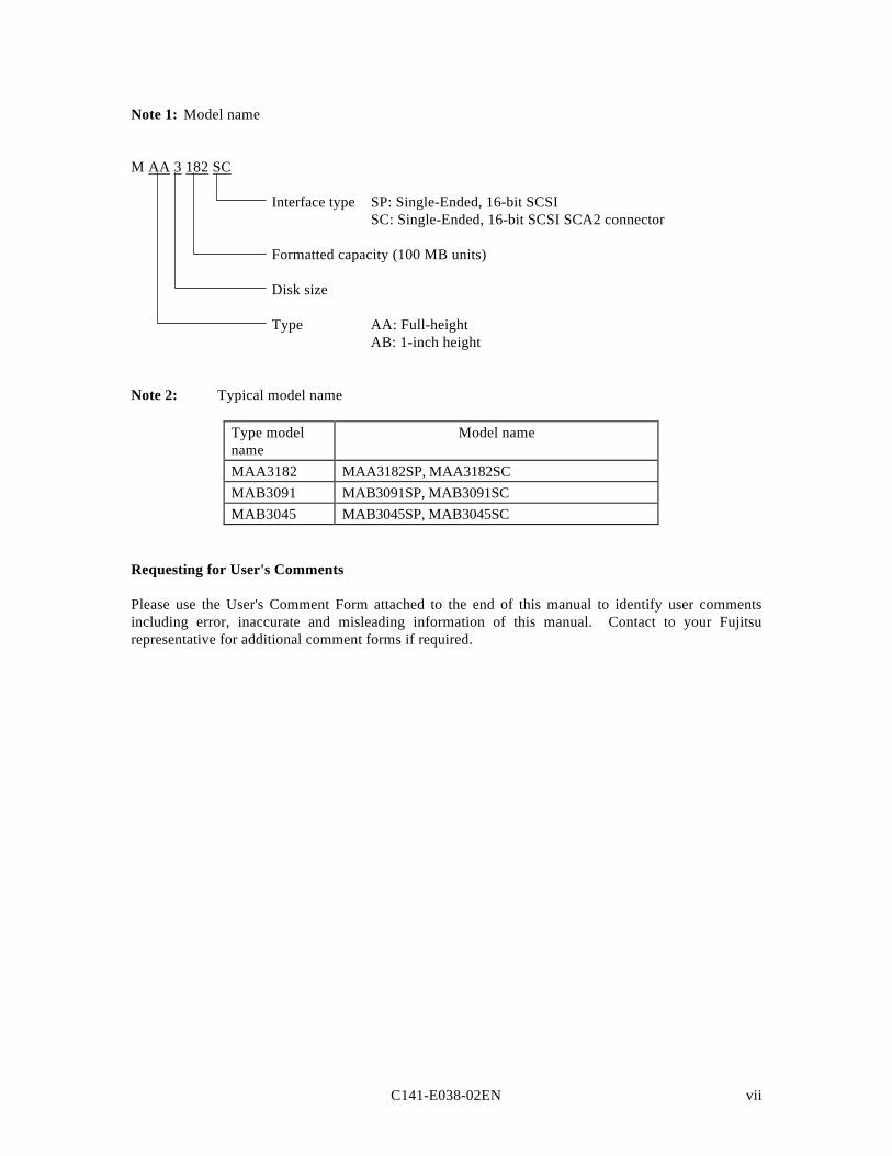
Note 1: Model name
M AA 3 182 SC
Interface type SP: Single-Ended, 16-bit SCSISC: Single-Ended, 16-bit SCSI SCA2 connector
Formatted capacity (100 MB units)
Disk size
Type AA: Full-heightAB: 1-inch height
Note 2: Typical model name
Type modelname
Model name
MAA3182 MAA3182SP, MAA3182SCMAB3091 MAB3091SP, MAB3091SCMAB3045 MAB3045SP, MAB3045SC
Requesting for User's Comments
Please use the User's Comment Form attached to the end of this manual to identify user commentsincluding error, inaccurate and misleading information of this manual. Contact to your Fujitsurepresentative for additional comment forms if required.
C141-E038-02ENviii
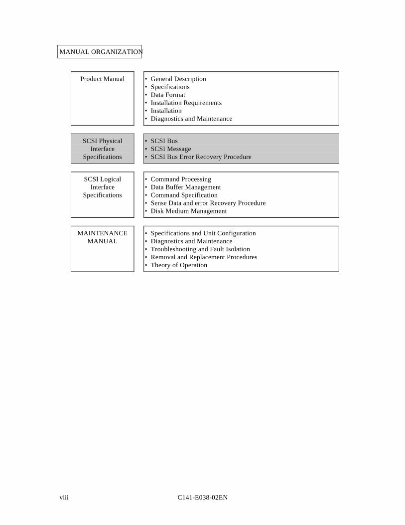
MANUAL ORGANIZATION
Product Manual • General Description• Specifications• Data Format• Installation Requirements• Installation• Diagnostics and Maintenance
SCSI PhysicalInterface
Specifications
• SCSI Bus• SCSI Message• SCSI Bus Error Recovery Procedure
SCSI LogicalInterface
Specifications
• Command Processing• Data Buffer Management• Command Specification• Sense Data and error Recovery Procedure• Disk Medium Management
MAINTENANCEMANUAL
• Specifications and Unit Configuration• Diagnostics and Maintenance• Troubleshooting and Fault Isolation• Removal and Replacement Procedures• Theory of Operation
C141-E038-02EN ix
CONTENTS
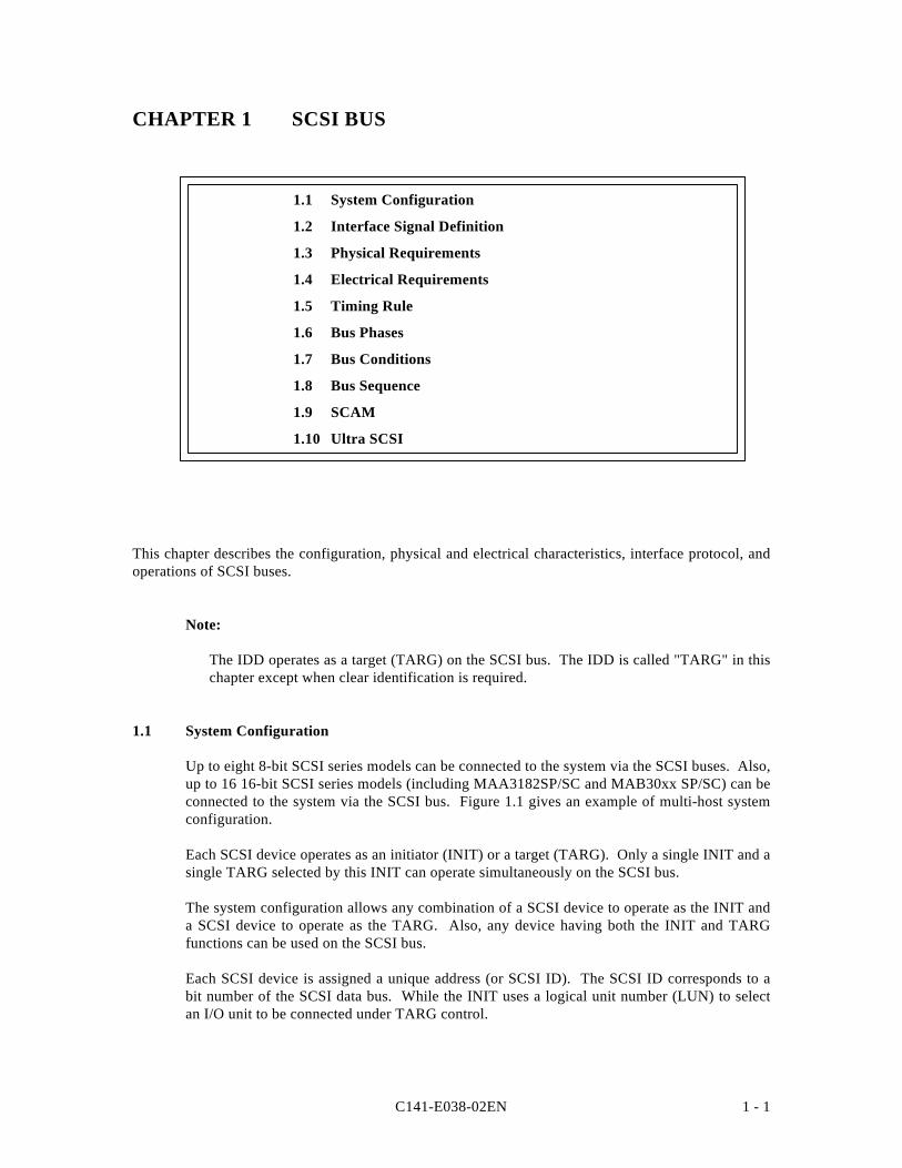
pageCHAPTER 1 SCSI BUS......................................................................................................... 1 - 1
1.1 System Configuration..................................................................................................... 1 - 1
1.2 Interface Signal Definition.............................................................................................. 1 - 3
1.3 Physical Requirements ................................................................................................... 1 - 6
1.3.1 Interface connector ......................................................................................................... 1 - 6
1.3.2 Interface cable................................................................................................................. 1 - 15
1.4 Electrical Requirements.................................................................................................. 1 - 17
1.4.1 Single-Ended type .......................................................................................................... 1 - 17
1.4.2 Power supply for terminating resistor............................................................................. 1 - 20
1.4.3 Signal driving conditions................................................................................................ 1 - 22
1.5 Timing Rule.................................................................................................................... 1 - 24
1.6 Bus Phases...................................................................................................................... 1 - 26
1.6.1 BUS FREE phase ........................................................................................................... 1 - 27
1.6.2 ARBITRATION phase ................................................................................................... 1 - 28
1.6.3 SELECTION phase ........................................................................................................ 1 - 31
1.6.4 RESELECTION phase ................................................................................................... 1 - 34
1.6.5 INFORMATION TRANSFER phases............................................................................ 1 - 36
1.6.6 COMMAND phase......................................................................................................... 1 - 44
1.6.7 DATA phase................................................................................................................... 1 - 44
1.6.8 STATUS phase............................................................................................................... 1 - 47
1.6.9 MESSAGE phase ........................................................................................................... 1 - 47
1.6.10 Signal requirements concerning transition between bus phases ..................................... 1 - 48
1.6.11 Time monitoring feature................................................................................................. 1 - 49
1.7 Bus Conditions ............................................................................................................... 1 - 50
1.7.1 ATTENTION condition.................................................................................................. 1 - 50
1.7.2 RESET condition............................................................................................................ 1 - 52
1.8 Bus Sequence ................................................................................................................. 1 - 53
1.9 SCAM ............................................................................................................................ 1 - 61
1.9.1 SCAM operations ........................................................................................................... 1 - 61
1.10 Ultra SCSI ...................................................................................................................... 1 - 66
1.10.1 Outline............................................................................................................................ 1 - 66
1.10.2 Device connection .......................................................................................................... 1 - 66
x C141-E038-02EN
1.10.3 Electrical characteristics of SCSI parallel interface ........................................................ 1 - 67
CHAPTER 2 SCSI MESSAGE ............................................................................................. 2 - 1
2.1 Message System ............................................................................................................. 2 - 1
2.1.1 Message format .............................................................................................................. 2 - 1
2.1.2 Message type .................................................................................................................. 2 - 2
2.1.3 Message protocol............................................................................................................ 2 - 4
2.2 SCSI Pointer ................................................................................................................... 2 - 5
2.3 Message Explanation...................................................................................................... 2 - 8
2.3.1 COMMAND COMPLETE message: X'00'(T→I) ......................................................... 2 - 8
2.3.2 SAVE DATA POINTER message: X'02'(T→I)............................................................. 2 - 8
2.3.3 DISCONNECT message: X'04' (T→I) ........................................................................... 2 - 8
2.3.4 INITIATOR DETECTED ERROR message: X'05'(I→T) ............................................. 2 - 9
2.3.5 ABORT message: X'06' (I→T)...................................................................................... 2 - 9
2.3.6 MESSAGE REJECT message: X'07'(I↔T)................................................................... 2 - 10
2.3.7 NO OPERATION message: X'08' (I→T) ...................................................................... 2 - 10
2.3.8 MESSAGE PARITY ERROR message: X'09' (I→T).................................................... 2 - 10
2.3.9 LINKED COMMAND COMPLETE message: X'0A'(T→I) ......................................... 2 - 10
2.3.10 LINKED COMMAND COMPLETE WITH FLAG message: X'0B'(T→I)................... 2 - 11
2.3.11 BUS DEVICE RESET message: X'0C' (I→T)............................................................... 2 - 11
2.3.12 ABORT TAG message: X'0D' (I→T)............................................................................ 2 - 11
2.3.13 CLEAR QUEUE message: X'0E'(I→T)......................................................................... 2 - 11
2.3.14 TERMINATE I/O PROCESS message: X'11' (I→T) .................................................... 2 - 12
2.3.15 QUEUE TAG messages.................................................................................................. 2 - 13
2.3.16 IDENTIFY message: X'80' to X'FF' (I↔T) ................................................................... 2 - 14
2.3.17 SYNCHRONOUS DATA TRANSFER REQUEST message(I↔T) .............................. 2 - 15
2.3.18 WIDE DATA TRANSFER REQUEST message (I↔T)................................................. 2 - 23
CHAPTER 3 ERROR RECOVERY .................................................................................... 3 - 1
3.1 Error Conditions and Retry Procedure............................................................................ 3 - 1
3.2 Recovery Control ........................................................................................................... 3 - 6
Glossary ...................................................................................................................................... GL - 1
Abbreviation ............................................................................................................................... AB - 1
C141-E038-02EN xi
FIGURES
page1.1 Example of SCSI configuration...................................................................................... 1 - 2
1.2 Interface signals.............................................................................................................. 1 - 3
1.3 DATA BUS and SCSI ID ............................................................................................... 1 - 4
1.4 SCSI interface connector (IDD side) (8-bit SCSI) .......................................................... 1 - 7
1.5 SCSI interface connector (cable side) (8-bit SCSI)......................................................... 1 - 8
1.6 Single-Ended connector pin assignments (8-bit SCSI) ................................................... 1 - 9
1.7 SCSI interface connector (IDD side) (16-bit SCSI) ........................................................ 1 - 10
1.8 SCSI interface connector (cable side) (16-bit SCSI)....................................................... 1 - 11
1.9 Single-ended connector pin assignment (16-bit SCSI) ................................................... 1 - 12
1.10 SCA type, single-ended 16-bit SCSI interface connector (IDD side) ............................. 1 - 13
1.11 SCA Type, single-ended 16-bit SCSI connector signal assignment ............................... 1 - 14
1.12 Connection of interface cable ......................................................................................... 1 - 16
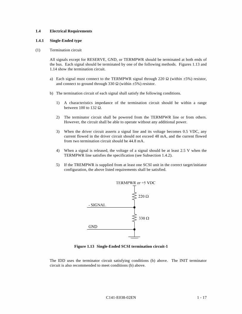
1.13 Single-Ended SCSI termination circuit-1 ....................................................................... 1 - 17
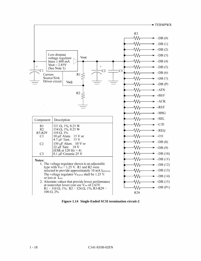
1.14 Single-Ended SCSI termination circuit-2 ....................................................................... 1 - 18
1.15 Single-ended terminating resistor circuit ........................................................................ 1 - 21
1.16 BUS FREE phase ........................................................................................................... 1 - 27
1.17 ARBITRATION phase ................................................................................................... 1 - 30
1.18 SELECTION phase ........................................................................................................ 1 - 33
1.19 RESELECTION phase ................................................................................................... 1 - 35
1.20 INFORMATION TRANSFER phase (phase control)..................................................... 1 - 36
1.21 Transfer in asynchronous mode...................................................................................... 1 - 39
1.22 Transfer in synchronous mode ....................................................................................... 1 - 42
1.23 Transfer in Fast synchronous mode................................................................................ 1 - 43
1.24 Data sequence at data transfer......................................................................................... 1 - 44
1.25 Data transfer rate in asynchronous mode........................................................................ 1 - 45
1.26 Data transfer rate in synchronous mode.......................................................................... 1 - 46
1.27 Switching direction of transfer over data bus ................................................................. 1 - 48
1.28 ATTENTION condition.................................................................................................. 1 - 51
1.29 RESET condition............................................................................................................ 1 - 53
1.30 Bus phase sequence ........................................................................................................ 1 - 54
1.31 Example of bus phase transition at execution of a single command............................... 1 - 56
1.32 State of level-1 SCAM target.......................................................................................... 1 - 63

xii C141-E038-02EN
1.33 State of level-2 SCAM target.......................................................................................... 1 - 64
1.34 Comparison of active negate current and voltage........................................................... 1 - 68
1.35 Unbalanced test circuit ................................................................................................... 1 - 69
2.1 Message format .............................................................................................................. 2 - 2
2.2 SCSI pointer configuration............................................................................................. 2 - 7
C141-E038-02EN xiii
TABLES
page1.1 INFORMATION TRANSFER phase identification ....................................................... 1 - 5
1.2 Interface cable requirements ........................................................................................... 1 - 15
1.3 Requirements for terminating resistor power supply ...................................................... 1 - 20
1.4 Signal status.................................................................................................................... 1 - 22
1.5 Signal driving method .................................................................................................... 1 - 22
1.6 Bus phases and signal sources........................................................................................ 1 - 23
1.7 Timing specifications ..................................................................................................... 1 - 24
1.8 Parameters used for fast synchronous data transfer mode .............................................. 1 - 46
1.9 Retry count setting for RESELECTION phase............................................................... 1 - 49
1.10 SCSI bus timing values .................................................................................................. 1 - 71
2.1 SCSI message ................................................................................................................. 2 - 3
2.2 Extended message .......................................................................................................... 2 - 4
2.3 Definition of data transfer mode by message exchange.................................................. 2 - 16
2.4 Synchronous mode data transfer request setting............................................................. 2 - 18
2.5 Transfer mode setup request from INIT to IDD.............................................................. 2 - 20
2.6 Transfer mode setup request from IDD to INIT.............................................................. 2 - 22
2.7 Data bus width defined by message exchange................................................................ 2 - 24
2.8 Wide mode setting request from the INIT to the IDD .................................................... 2 - 26
2.9 Wide mode setting request from the IDD to the INIT .................................................... 2 - 27
3.1 Retry procedure for SCSI error....................................................................................... 3 - 7

C141-E038-02EN 1 - 1
CHAPTER 1 SCSI BUS
1.1 System Configuration
1.2 Interface Signal Definition
1.3 Physical Requirements
1.4 Electrical Requirements
1.5 Timing Rule
1.6 Bus Phases
1.7 Bus Conditions
1.8 Bus Sequence
1.9 SCAM
1.10 Ultra SCSI
This chapter describes the configuration, physical and electrical characteristics, interface protocol, andoperations of SCSI buses.
Note:
The IDD operates as a target (TARG) on the SCSI bus. The IDD is called "TARG" in thischapter except when clear identification is required.
1.1 System Configuration
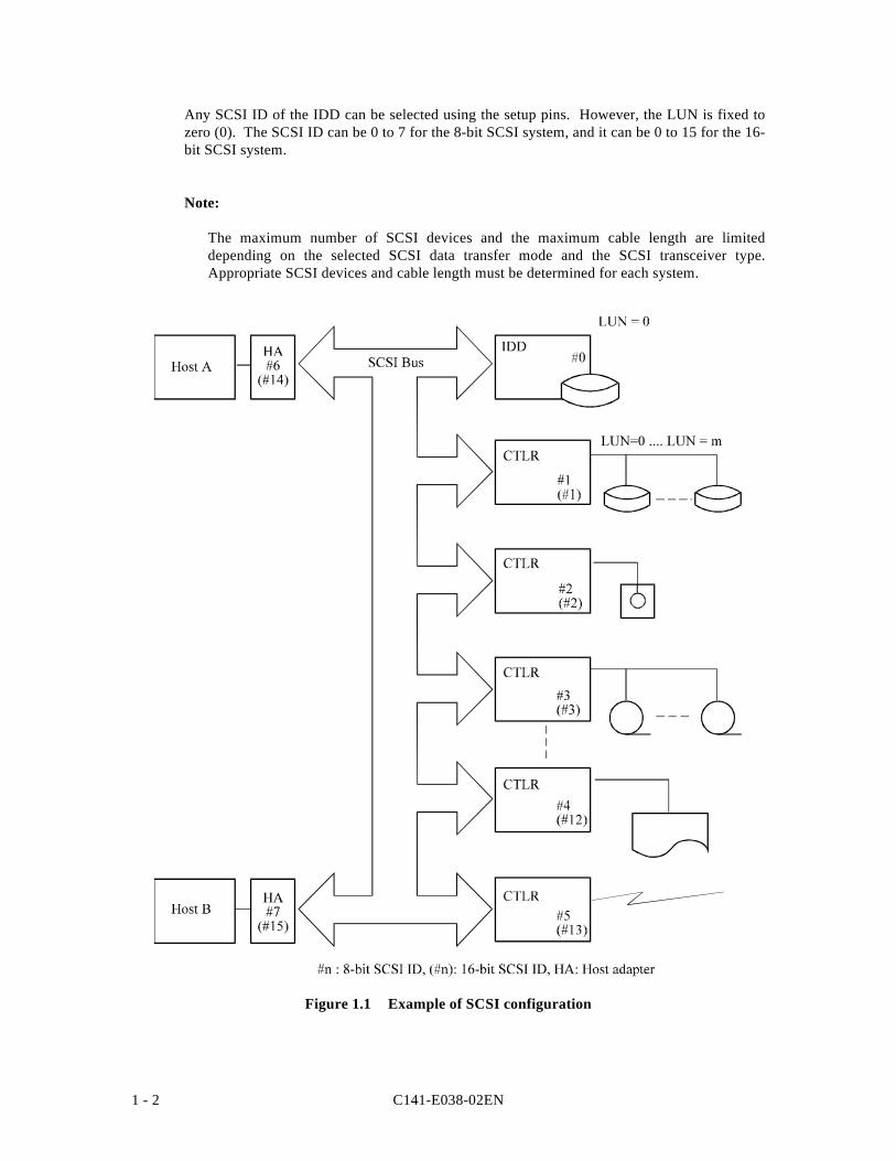
Up to eight 8-bit SCSI series models can be connected to the system via the SCSI buses. Also,up to 16 16-bit SCSI series models (including MAA3182SP/SC and MAB30xx SP/SC) can beconnected to the system via the SCSI bus. Figure 1.1 gives an example of multi-host systemconfiguration.
Each SCSI device operates as an initiator (INIT) or a target (TARG). Only a single INIT and asingle TARG selected by this INIT can operate simultaneously on the SCSI bus.
The system configuration allows any combination of a SCSI device to operate as the INIT anda SCSI device to operate as the TARG. Also, any device having both the INIT and TARGfunctions can be used on the SCSI bus.
Each SCSI device is assigned a unique address (or SCSI ID). The SCSI ID corresponds to abit number of the SCSI data bus. While the INIT uses a logical unit number (LUN) to selectan I/O unit to be connected under TARG control.
C141-E038-02EN1 - 2
Any SCSI ID of the IDD can be selected using the setup pins. However, the LUN is fixed tozero (0). The SCSI ID can be 0 to 7 for the 8-bit SCSI system, and it can be 0 to 15 for the 16-bit SCSI system.
Note:
The maximum number of SCSI devices and the maximum cable length are limiteddepending on the selected SCSI data transfer mode and the SCSI transceiver type.Appropriate SCSI devices and cable length must be determined for each system.
Figure 1.1 Example of SCSI configuration
C141-E038-02EN 1 - 3
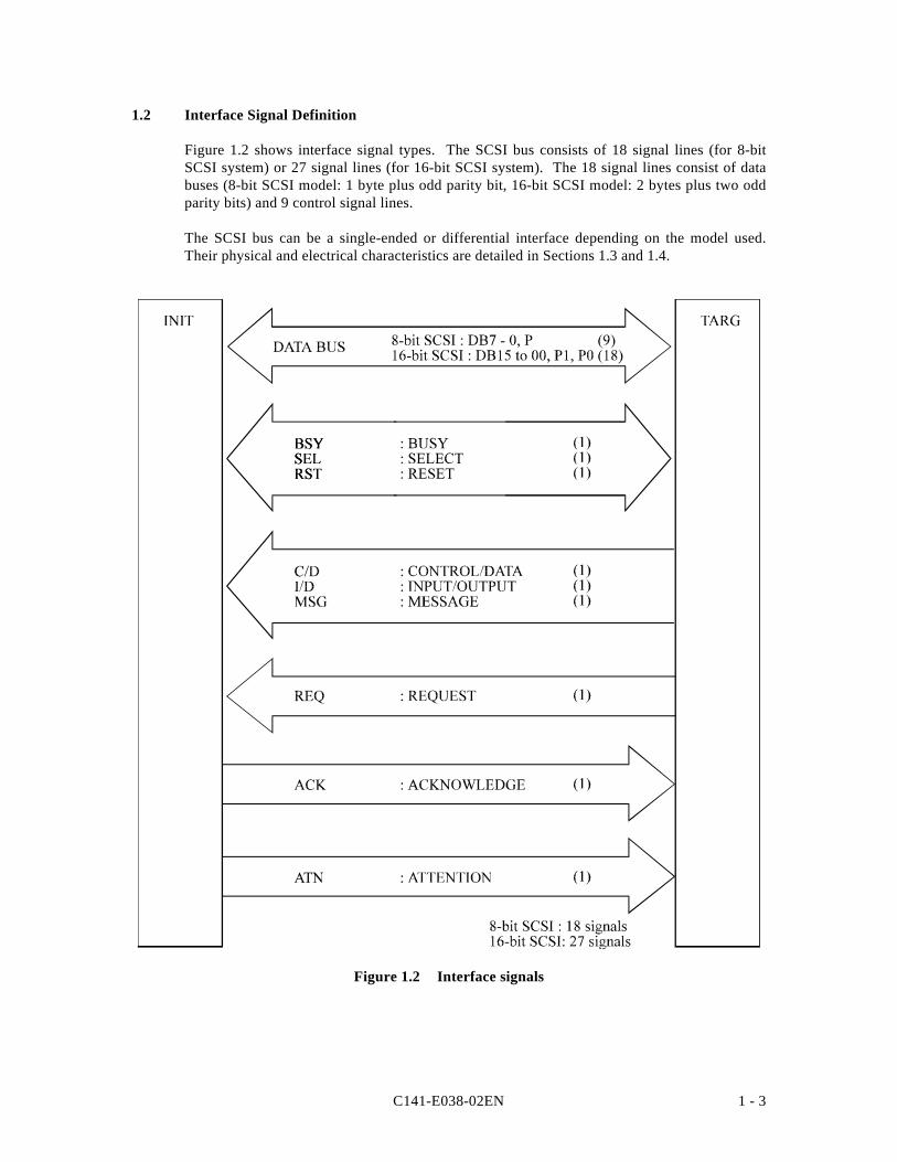
1.2 Interface Signal Definition
Figure 1.2 shows interface signal types. The SCSI bus consists of 18 signal lines (for 8-bitSCSI system) or 27 signal lines (for 16-bit SCSI system). The 18 signal lines consist of databuses (8-bit SCSI model: 1 byte plus odd parity bit, 16-bit SCSI model: 2 bytes plus two oddparity bits) and 9 control signal lines.
The SCSI bus can be a single-ended or differential interface depending on the model used.Their physical and electrical characteristics are detailed in Sections 1.3 and 1.4.
Figure 1.2 Interface signals
C141-E038-02EN1 - 4
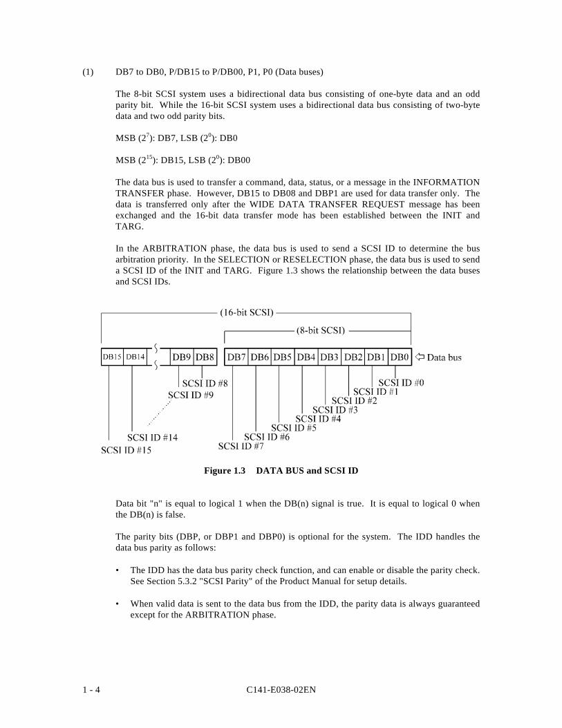
(1) DB7 to DB0, P/DB15 to P/DB00, P1, P0 (Data buses)
The 8-bit SCSI system uses a bidirectional data bus consisting of one-byte data and an oddparity bit. While the 16-bit SCSI system uses a bidirectional data bus consisting of two-bytedata and two odd parity bits.
MSB (27): DB7, LSB (20): DB0
MSB (215): DB15, LSB (20): DB00
The data bus is used to transfer a command, data, status, or a message in the INFORMATIONTRANSFER phase. However, DB15 to DB08 and DBP1 are used for data transfer only. Thedata is transferred only after the WIDE DATA TRANSFER REQUEST message has beenexchanged and the 16-bit data transfer mode has been established between the INIT andTARG.
In the ARBITRATION phase, the data bus is used to send a SCSI ID to determine the busarbitration priority. In the SELECTION or RESELECTION phase, the data bus is used to senda SCSI ID of the INIT and TARG. Figure 1.3 shows the relationship between the data busesand SCSI IDs.
Figure 1.3 DATA BUS and SCSI ID
Data bit "n" is equal to logical 1 when the DB(n) signal is true. It is equal to logical 0 whenthe DB(n) is false.
The parity bits (DBP, or DBP1 and DBP0) is optional for the system. The IDD handles thedata bus parity as follows:
• The IDD has the data bus parity check function, and can enable or disable the parity check.See Section 5.3.2 "SCSI Parity" of the Product Manual for setup details.
• When valid data is sent to the data bus from the IDD, the parity data is always guaranteedexcept for the ARBITRATION phase.
C141-E038-02EN 1 - 5
(2) BSY (BUSY)
The BSY signal indicates that the SCSI bus is in use. In the ARBITRATION phase, thissignal is used to request for the bus usage priority.
(3) SEL (SELECT)
The SEL signal is used by the INIT to select a TARG (in the SELECTION phase) or by theTARG to reselect an INIT (in the RESELECTION phase).
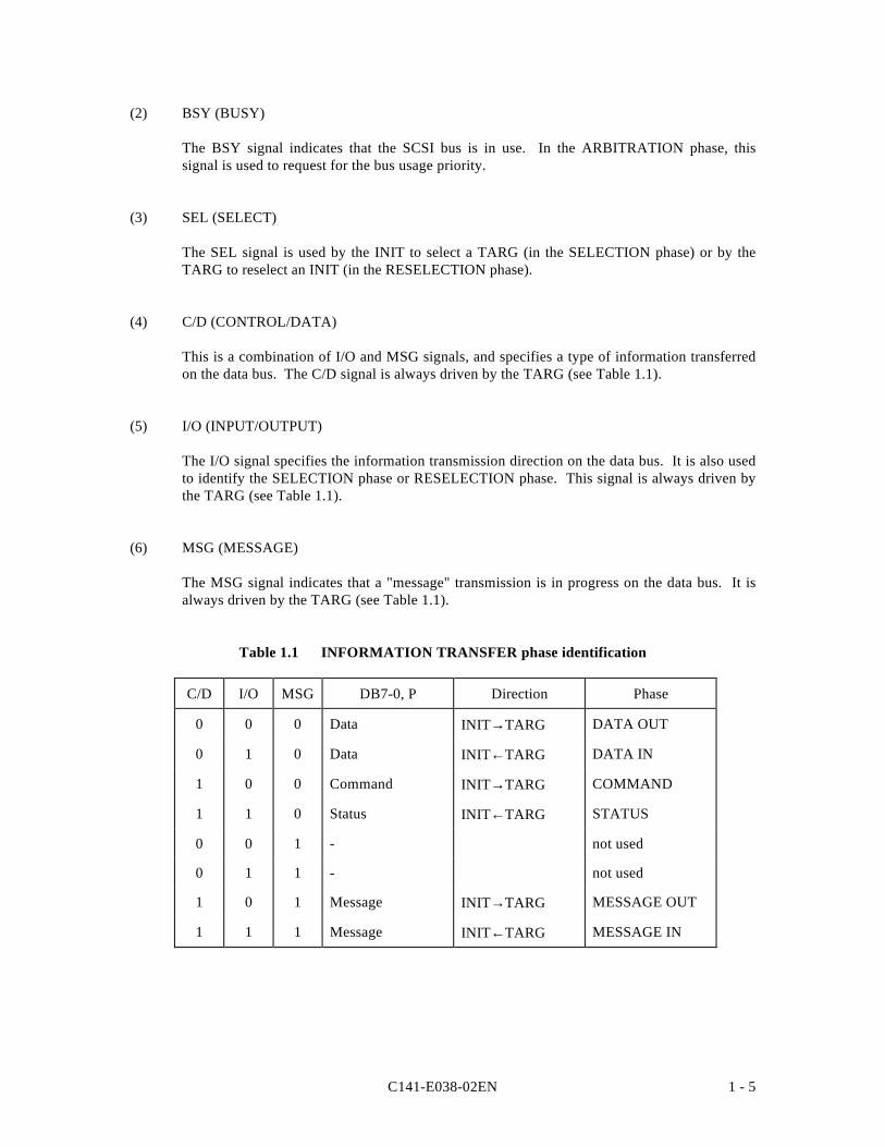
(4) C/D (CONTROL/DATA)
This is a combination of I/O and MSG signals, and specifies a type of information transferredon the data bus. The C/D signal is always driven by the TARG (see Table 1.1).
(5) I/O (INPUT/OUTPUT)
The I/O signal specifies the information transmission direction on the data bus. It is also usedto identify the SELECTION phase or RESELECTION phase. This signal is always driven bythe TARG (see Table 1.1).
(6) MSG (MESSAGE)
The MSG signal indicates that a "message" transmission is in progress on the data bus. It isalways driven by the TARG (see Table 1.1).
Table 1.1 INFORMATION TRANSFER phase identification
C/D I/O MSG DB7-0, P Direction Phase
0 0 0 Data INIT→TARG DATA OUT
0 1 0 Data INIT←TARG DATA IN
1 0 0 Command INIT→TARG COMMAND
1 1 0 Status INIT←TARG STATUS
0 0 1 - not used
0 1 1 - not used
1 0 1 Message INIT→TARG MESSAGE OUT
1 1 1 Message INIT←TARG MESSAGE IN
C141-E038-02EN1 - 6
(7) REQ (REQUEST)
This is a transmission request from the TARG to the INIT in the INFORMATIONTRANSFER phase.
(8) ACK (ACKNOWLEDGE)
The ACK signal is a response to the REQ signal sent from the INIT to TARG in theINFORMATION TRANSFER phase.
(9) ATN (ATTENTION)
The ATN signal indicates that the INIT has a message to be sent to the TARG. It is used togenerate an ATTENTION condition.
(10) RST (RESET)
The RST signal is a Reset signal to clear all SCSI devices on the bus (to the RESETcondition).
1.3 Physical Requirements
All SCSI devices are connected to each other in a daisy chain. Both ends of the interface cableare terminated with resistor.
The following defines the SCSI bus electrical characteristics (for interface signaldriver/receiver).
• Single-ended (Unbalanced transmission type):Maximum cable length: 6 m
For 16-bit SCSI bus:Maximum cable length: 6 m (at 10 MBps or less transmission rate)Maximum cable length: 3 m (at 10 MBps or less transmission rate)
1.3.1 Interface connector
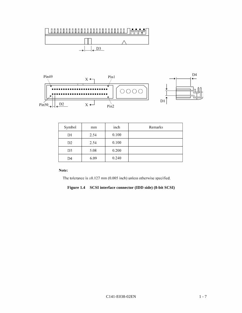
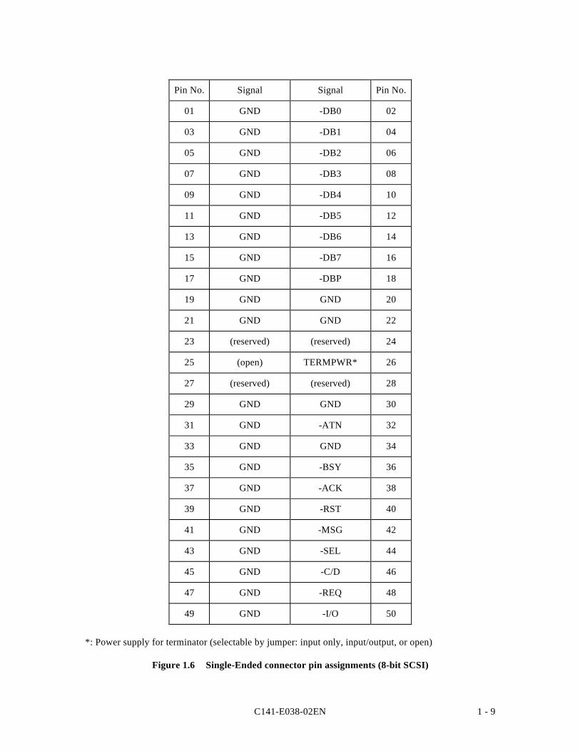
(1) Interface connector of 8-bit SCSI
The 8-bit SCSI bus connectors of the IDD are 50-pin, unshielded connectors, each having tworows of 25 parallel pins (separated 2.54 mm or 0.1" from each other) (see Figure 1.4).
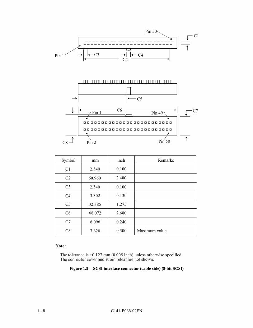
Use the 50-pin, unshielded pin socket, having two rows of 25 parallel pins (separated 2.54 mmor 0.1" from each other). Also, a keyed connector (with a band) to prevent an incorrect cableinsertion is desirable to use (see Figure 1.5).
Figure 1.6 shows the standard pin assignment of single-ended interface connectors.
C141-E038-02EN 1 - 7
Figure 1.4 SCSI interface connector (IDD side) (8-bit SCSI)
C141-E038-02EN1 - 8
Figure 1.5 SCSI interface connector (cable side) (8-bit SCSI)
C141-E038-02EN 1 - 9
Pin No. Signal Signal Pin No.
01 GND -DB0 02
03 GND -DB1 04
05 GND -DB2 06
07 GND -DB3 08
09 GND -DB4 10
11 GND -DB5 12
13 GND -DB6 14
15 GND -DB7 16
17 GND -DBP 18
19 GND GND 20
21 GND GND 22
23 (reserved) (reserved) 24
25 (open) TERMPWR* 26
27 (reserved) (reserved) 28
29 GND GND 30
31 GND -ATN 32
33 GND GND 34
35 GND -BSY 36
37 GND -ACK 38
39 GND -RST 40
41 GND -MSG 42
43 GND -SEL 44
45 GND -C/D 46
47 GND -REQ 48
49 GND -I/O 50
*: Power supply for terminator (selectable by jumper: input only, input/output, or open)
Figure 1.6 Single-Ended connector pin assignments (8-bit SCSI)
C141-E038-02EN1 - 10
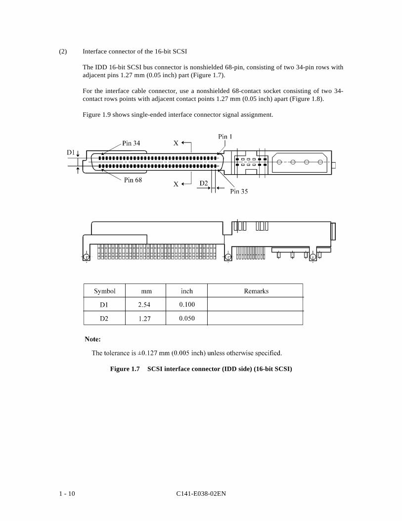
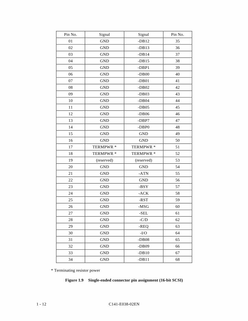
(2) Interface connector of the 16-bit SCSI
The IDD 16-bit SCSI bus connector is nonshielded 68-pin, consisting of two 34-pin rows withadjacent pins 1.27 mm (0.05 inch) part (Figure 1.7).
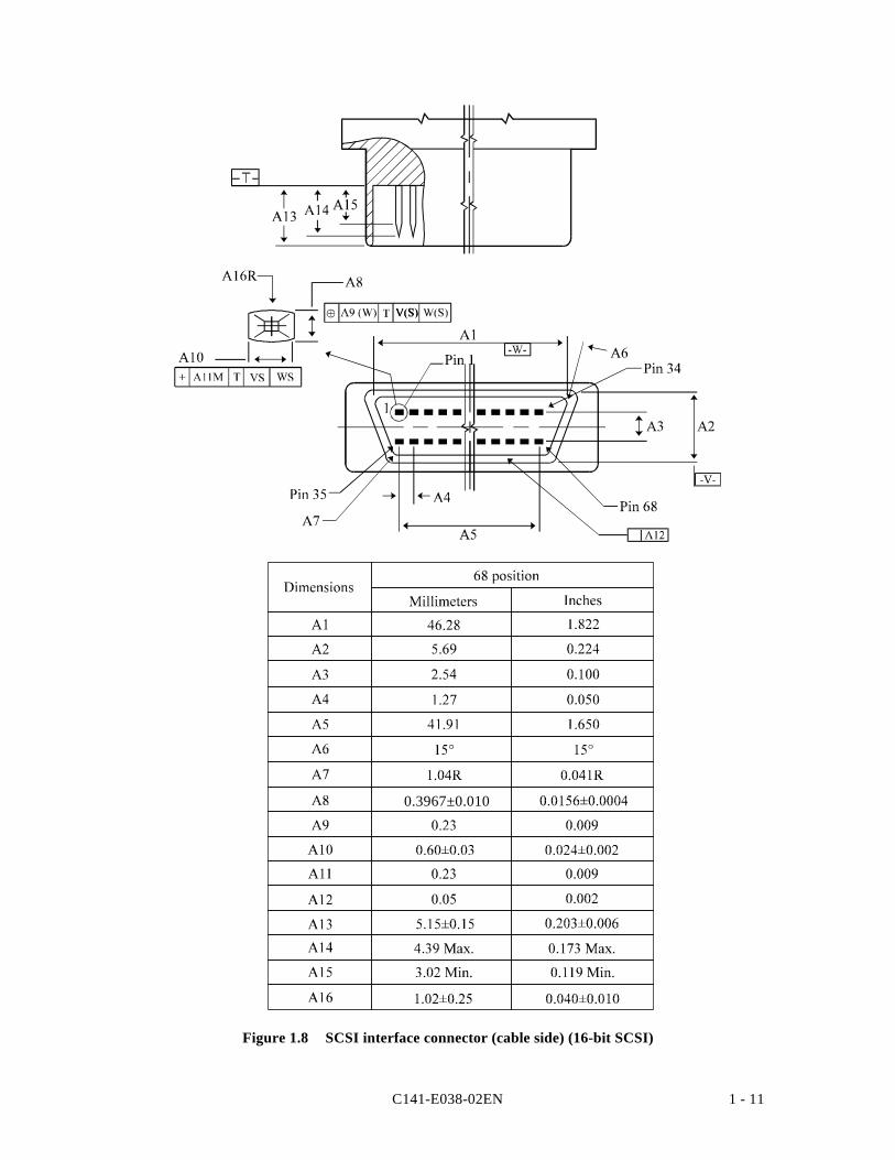
For the interface cable connector, use a nonshielded 68-contact socket consisting of two 34-contact rows points with adjacent contact points 1.27 mm (0.05 inch) apart (Figure 1.8).
Figure 1.9 shows single-ended interface connector signal assignment.
Figure 1.7 SCSI interface connector (IDD side) (16-bit SCSI)
C141-E038-02EN 1 - 11
Figure 1.8 SCSI interface connector (cable side) (16-bit SCSI)
0.3967±0.010
C141-E038-02EN1 - 12
Pin No. Signal Signal Pin No.
01 GND -DB12 35
02 GND -DB13 36
03 GND -DB14 37
04 GND -DB15 38
05 GND -DBP1 39
06 GND -DB00 40
07 GND -DB01 41
08 GND -DB02 42
09 GND -DB03 43
10 GND -DB04 44
11 GND -DB05 45
12 GND -DB06 46
13 GND -DBP7 47
14 GND -DBP0 48
15 GND GND 49
16 GND GND 50
17 TERMPWR * TERMPWR * 51
18 TERMPWR * TERMPWR * 52
19 (reserved) (reserved) 53
20 GND GND 54
21 GND -ATN 55
22 GND GND 56
23 GND -BSY 57
24 GND -ACK 58
25 GND -RST 59
26 GND -MSG 60
27 GND -SEL 61
28 GND -C/D 62
29 GND -REQ 63
30 GND -I/O 64
31 GND -DB08 65
32 GND -DB09 66
33 GND -DB10 67
34 GND -DB11 68
* Terminating resistor power
Figure 1.9 Single-ended connector pin assignment (16-bit SCSI)
C141-E038-02EN 1 - 13
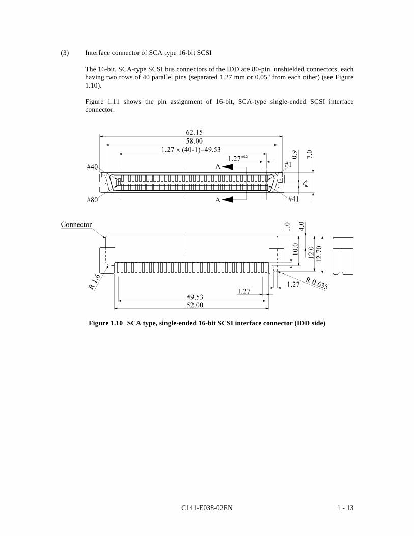
(3) Interface connector of SCA type 16-bit SCSI
The 16-bit, SCA-type SCSI bus connectors of the IDD are 80-pin, unshielded connectors, eachhaving two rows of 40 parallel pins (separated 1.27 mm or 0.05" from each other) (see Figure1.10).
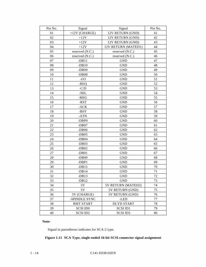
Figure 1.11 shows the pin assignment of 16-bit, SCA-type single-ended SCSI interfaceconnector.
Figure 1.10 SCA type, single-ended 16-bit SCSI interface connector (IDD side)
C141-E038-02EN1 - 14
Pin No. Signal Signal Pin No.01 +12V (CHARGE) 12V RETURN (GND) 4102 +12V 12V RETURN (GND) 4203 +12V 12V RETURN (GND) 4304 +12V 12V RETURN (MATED1) 4405 reserved (N.C.) reserved (N.C.) 4506 reserved (N.C.) reserved (N.C.) 4607 -DB11 GND 4708 -DB10 GND 4809 -DB09 GND 4910 -DB08 GND 5011 -I/O GND 5112 -REQ GND 5213 -C/D GND 5314 -SEL GND 5415 -MSG GND 5516 -RST GND 5617 -ACK GND 5718 -BSY GND 5819 -ATN GND 5920 -DBP0 GND 6021 -DB07 GND 6122 -DB06 GND 6223 -DB05 GND 6324 -DB04 GND 6425 -DB03 GND 6526 -DB02 GND 6627 -DB01 GND 6728 -DB00 GND 6829 -DBP1 GND 6930 -DB15 GND 7031 -DB14 GND 7132 -DB13 GND 7233 -DB12 GND 7334 5V 5V RETURN (MATED2) 7435 5V 5V RETURN (GND) 7536 5V (CHARGE) 5V RETURN (GND) 7637 -SPINDLE SYNC -LED 7738 RMT START DLYD START 7839 SCSI ID0 SCSI ID1 7940 SCSI ID2 SCSI ID3 80
Note:
Signal in parentheses indicates for SCA-2 type.
Figure 1.11 SCA Type, single-ended 16-bit SCSI connector signal assignment
C141-E038-02EN 1 - 15
1.3.2 Interface cable
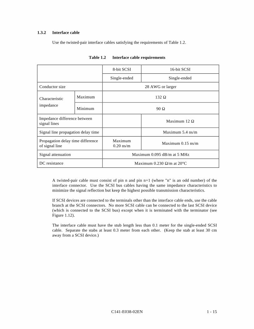
Use the twisted-pair interface cables satisfying the requirements of Table 1.2.
Table 1.2 Interface cable requirements
8-bit SCSI 16-bit SCSI
Single-ended Single-ended
Conductor size 28 AWG or larger
Characteristic Maximum 132 Ω
impedanceMinimum 90 Ω
Impedance difference betweensignal lines Maximum 12 Ω
Signal line propagation delay time Maximum 5.4 ns/m
Propagation delay time differenceof signal line
Maximum0.20 ns/m Maximum 0.15 ns/m
Signal attenuation Maximum 0.095 dB/m at 5 MHz
DC resistance Maximum 0.230 Ω/m at 20°C
A twisted-pair cable must consist of pin n and pin n+1 (where "n" is an odd number) of theinterface connector. Use the SCSI bus cables having the same impedance characteristics tominimize the signal reflection but keep the highest possible transmission characteristics.
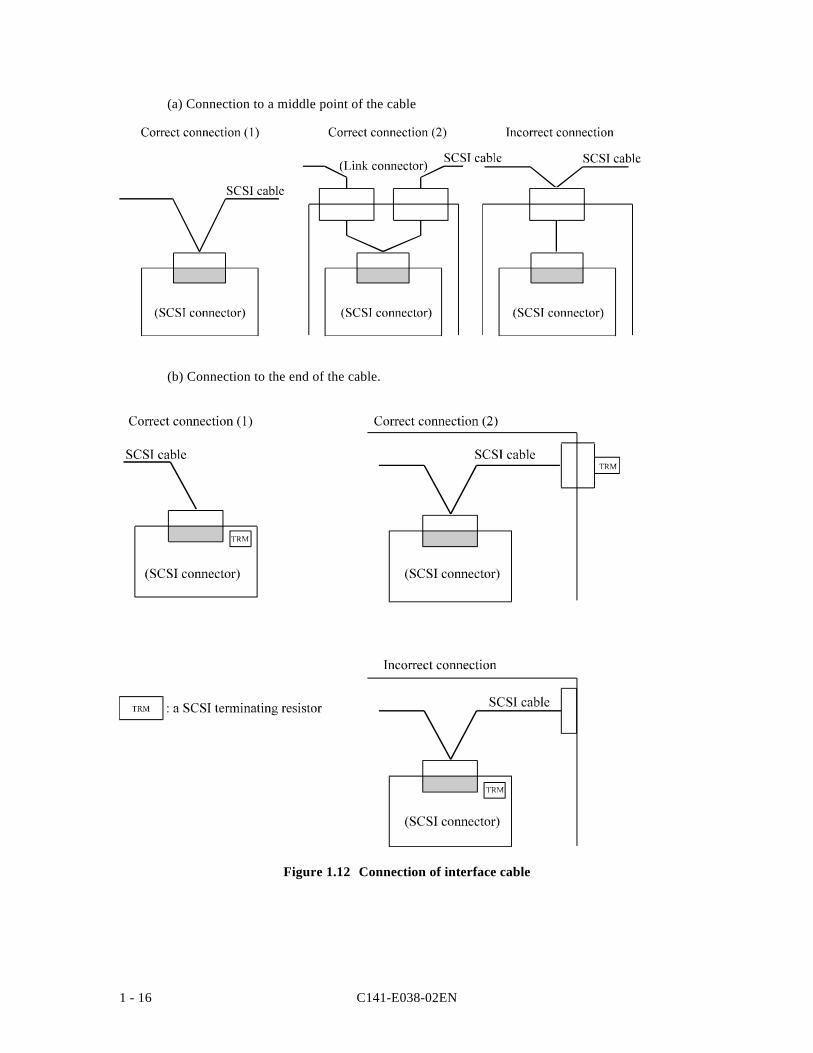
If SCSI devices are connected to the terminals other than the interface cable ends, use the cablebranch at the SCSI connectors. No more SCSI cable can be connected to the last SCSI device(which is connected to the SCSI bus) except when it is terminated with the terminator (seeFigure 1.12).
The interface cable must have the stub length less than 0.1 meter for the single-ended SCSIcable. Separate the stabs at least 0.3 meter from each other. (Keep the stab at least 30 cmaway from a SCSI device.)
C141-E038-02EN1 - 16
(a) Connection to a middle point of the cable
(b) Connection to the end of the cable.
Figure 1.12 Connection of interface cable
C141-E038-02EN 1 - 17
1.4 Electrical Requirements
1.4.1 Single-Ended type
(1) Termination circuit
All signals except for RESERVE, GND, or TERMPWR should be terminated at both ends ofthe bus. Each signal should be terminated by one of the following methods. Figures 1.13 and1.14 show the termination circuit.
a) Each signal must connect to the TERMPWR signal through 220 Ω (within ±5%) resistor,and connect to ground through 330 Ω (within ±5%) resistor.
b) The termination circuit of each signal shall satisfy the following conditions.
1) A characteristics impedance of the termination circuit should be within a rangebetween 100 to 132 Ω.
2) The terminator circuit shall be powered from the TERMPWR line or from others.However, the circuit shall be able to operate without any additional power.
3) When the driver circuit asserts a signal line and its voltage becomes 0.5 VDC, anycurrent flowed in the driver circuit should not exceed 48 mA, and the current flowedfrom two termination circuit should be 44.8 mA.
4) When a signal is released, the voltage of a signal should be at least 2.5 V when theTERMPWR line satisfies the specification (see Subsection 1.4.2).
5) If the TREMPWR is supplied from at least one SCSI unit in the correct target/initiatorconfiguration, the above listed requirements shall be satisfied.
Figure 1.13 Single-Ended SCSI termination circuit-1
The IDD uses the terminator circuit satisfying conditions (b) above. The INIT terminatorcircuit is also recommended to meet conditions (b) above.
C141-E038-02EN1 - 18
Figure 1.14 Single-Ended SCSI termination circuit-2
C141-E038-02EN 1 - 19
(2) Driver and receiver
For the interface signal driver, an open-collector or tri-state buffer that satisfies the followingoutput characteristics is used. All signals are negative logic (true = "L").
The receiver and non-driver of the SCSI device under the power-on state should satisfy thefollowing input characteristics on each signal.
[Output characteristic]VOL = 0.0 to 0.50 VDC (@ IOL = 48 mA)VOH = 2.5 to 5.25 VDC
[Input characteristics]VIL = 0.0 to 0.80 VDCVIH = 2.0 to 5.25 VDCIIL = -0.4 to 0.0 mA (@ VI = 0.5 VDC)IIH = 0.0 to 0.1 mA (@ VI = 2.7 VDC)Input hysteresis = 0.2 VDC min.Input capacity = 25 pF max.
Note:
The SCSI device under the power-off state should satisfy the characteristics of IIL and IIH.
[Recommended circuit example]Driver: MB463 (Fujitsu) or SN7438 (TI) (Open-collector NAND gate)Receiver: SN74LS240 or SN74LS19 (TI) (Shumitt trigger input inverter)
C141-E038-02EN1 - 20
1.4.2 Power supply for terminating resistor
The TERMPWR signal of the interface connector supplies the power to the terminatingresistor circuit connected to both ends of the cable. To attach a terminating resistor to anexternal SCSI device or to cut the power of SCSI device having a terminator, the terminatorpower must be supplied to the TERMPWR line from any of SCSI devices of the bus. TheSCSI device (such as a host adapter) which always operates as the INIT should supply thepower. The terminating resistor power shall be supplied to the TERMPWR line through adiode to prevent a reverse current.
Table 1.3 lists the requirements for terminating the resistor power supply (Vterm).
Table 1.3 Requirements for terminating resistor power supply
Single-ended type
Output voltage 4.25 to 5.25 VDC
Current capacity 900 mA min.
Sink current 1.0 mA max.
Figure 1.15 shows the configuration of a single-ended SCSI terminating resistor circuit. Thecircuit shall be set in either mode (by the CN7 setup pin) depending on the IDD systemrequirements.
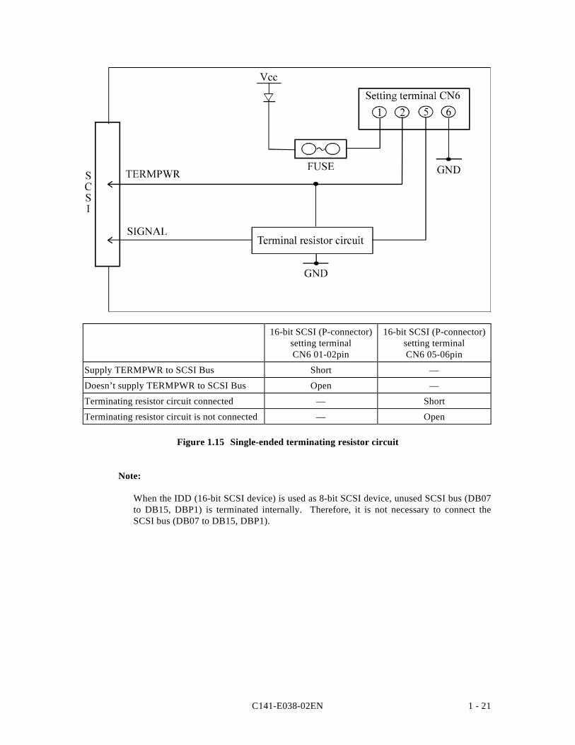
C141-E038-02EN 1 - 21
16-bit SCSI (P-connector)setting terminalCN6 01-02pin
16-bit SCSI (P-connector)setting terminalCN6 05-06pin
Supply TERMPWR to SCSI Bus Short —
Doesn’t supply TERMPWR to SCSI Bus Open —
Terminating resistor circuit connected — Short
Terminating resistor circuit is not connected — Open
Figure 1.15 Single-ended terminating resistor circuit
Note:
When the IDD (16-bit SCSI device) is used as 8-bit SCSI device, unused SCSI bus (DB07to DB15, DBP1) is terminated internally. Therefore, it is not necessary to connect theSCSI bus (DB07 to DB15, DBP1).
C141-E038-02EN1 - 22
1.4.3 Signal driving conditions
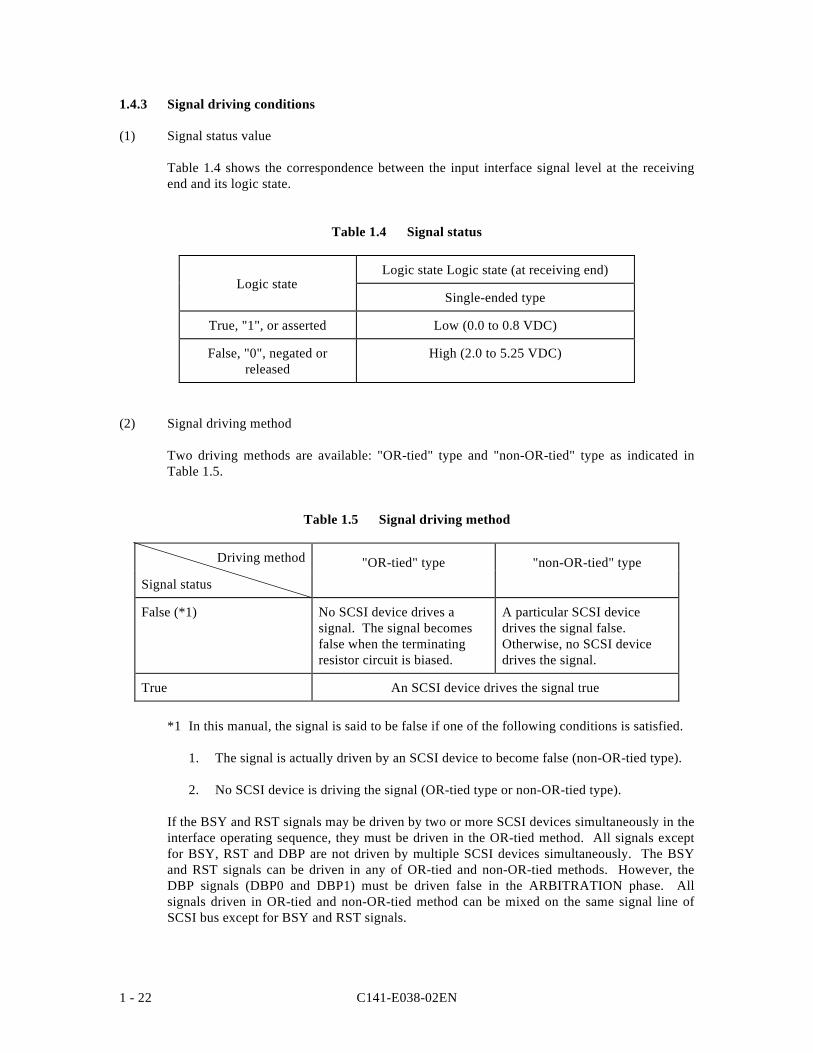
(1) Signal status value
Table 1.4 shows the correspondence between the input interface signal level at the receivingend and its logic state.
Table 1.4 Signal status
Logic state Logic state (at receiving end)
Single-ended type
True, "1", or asserted Low (0.0 to 0.8 VDC)
False, "0", negated orreleased
High (2.0 to 5.25 VDC)
(2) Signal driving method
Two driving methods are available: "OR-tied" type and "non-OR-tied" type as indicated inTable 1.5.
Table 1.5 Signal driving method
Driving method "OR-tied" type "non-OR-tied" type
Signal status
False (*1) No SCSI device drives asignal. The signal becomesfalse when the terminatingresistor circuit is biased.
A particular SCSI devicedrives the signal false.Otherwise, no SCSI devicedrives the signal.
True An SCSI device drives the signal true
*1 In this manual, the signal is said to be false if one of the following conditions is satisfied.
1. The signal is actually driven by an SCSI device to become false (non-OR-tied type).
2. No SCSI device is driving the signal (OR-tied type or non-OR-tied type).
If the BSY and RST signals may be driven by two or more SCSI devices simultaneously in theinterface operating sequence, they must be driven in the OR-tied method. All signals exceptfor BSY, RST and DBP are not driven by multiple SCSI devices simultaneously. The BSYand RST signals can be driven in any of OR-tied and non-OR-tied methods. However, theDBP signals (DBP0 and DBP1) must be driven false in the ARBITRATION phase. Allsignals driven in OR-tied and non-OR-tied method can be mixed on the same signal line ofSCSI bus except for BSY and RST signals.
Logic state
C141-E038-02EN 1 - 23
(3) Signal sources
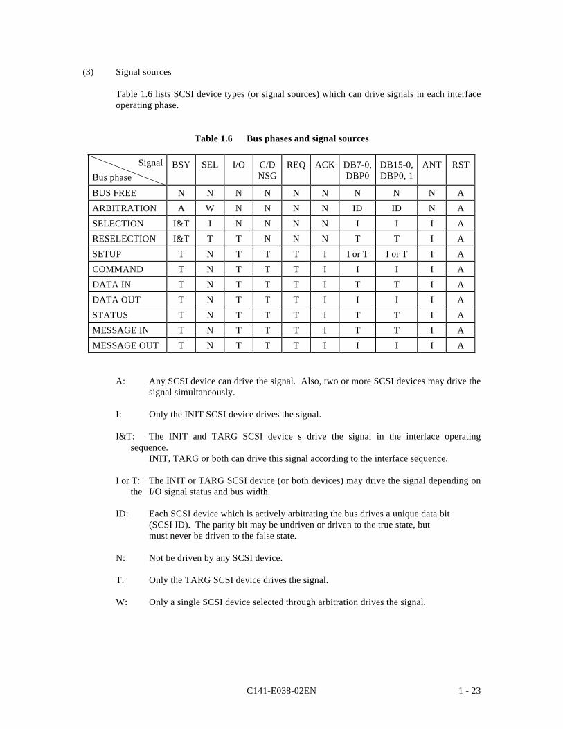
Table 1.6 lists SCSI device types (or signal sources) which can drive signals in each interfaceoperating phase.
Table 1.6 Bus phases and signal sources
Signal
Bus phaseBSY SEL I/O C/D
NSGREQ ACK DB7-0,
DBP0DB15-0,DBP0, 1
ANT RST
BUS FREE N N N N N N N N N A
ARBITRATION A W N N N N ID ID N A
SELECTION I&T I N N N N I I I A
RESELECTION I&T T T N N N T T I A
SETUP T N T T T I I or T I or T I A
COMMAND T N T T T I I I I A
DATA IN T N T T T I T T I A
DATA OUT T N T T T I I I I A
STATUS T N T T T I T T I A
MESSAGE IN T N T T T I T T I A
MESSAGE OUT T N T T T I I I I A
A: Any SCSI device can drive the signal. Also, two or more SCSI devices may drive thesignal simultaneously.
I: Only the INIT SCSI device drives the signal.
I&T: The INIT and TARG SCSI device s drive the signal in the interface operatingsequence.
INIT, TARG or both can drive this signal according to the interface sequence.
I or T: The INIT or TARG SCSI device (or both devices) may drive the signal depending onthe I/O signal status and bus width.
ID: Each SCSI device which is actively arbitrating the bus drives a unique data bit(SCSI ID). The parity bit may be undriven or driven to the true state, butmust never be driven to the false state.
N: Not be driven by any SCSI device.
T: Only the TARG SCSI device drives the signal.
W: Only a single SCSI device selected through arbitration drives the signal.
C141-E038-02EN1 - 24
1.5 Timing Rule
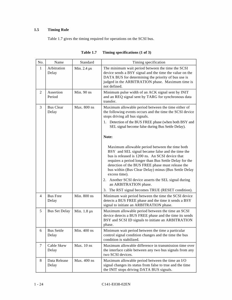
Table 1.7 gives the timing required for operations on the SCSI bus.
Table 1.7 Timing specifications (1 of 3)
No. Name Standard Timing specification1 Arbitration
DelayMin. 2.4 µs The minimum wait period between the time the SCSI
device sends a BSY signal and the time the value on theDATA BUS for determining the priority of bus use isjudged in the ARBITRATION phase. Maximum time isnot defined.
2 AssertionPeriod
Min. 90 ns Minimum pulse width of an ACK signal sent by INITand an REQ signal sent by TARG for synchronous datatransfer.
3 Bus ClearDelay
Max. 800 ns Maximum allowable period between the time either ofthe following events occurs and the time the SCSI devicestops driving all bus signals.1. Detection of the BUS FREE phase (when both BSY and
SEL signal become false during Bus Settle Delay).
Note:
Maximum allowable period between the time bothBSY and SEL signal became false and the time thebus is released is 1200 ns. An SCSI device thatrequires a period longer than Bus Settle Delay for thedetection of the BUS FREE phase must release thebus within (Bus Clear Delay) minus (Bus Settle Delayexcess time).
2. Another SCSI device asserts the SEL signal duringan ARBITRATION phase.
3. The RST signal becomes TRUE (RESET condition).4 Bus Free
DelayMin. 800 ns Minimum wait period between the time the SCSI device
detects a BUS FREE phase and the time it sends a BSYsignal to initiate an ARBITRATION phase.
5 Bus Set Delay Min. 1.8 µs Maximum allowable period between the time an SCSIdevice detects a BUS FREE phase and the time its sendsBSY and SCSI ID signals to initiate an ARBITRATIONphase.
6 Bus SettleDelay
Min. 400 ns Minimum wait period between the time a particularcontrol signal condition changes and the time the buscondition is stabilized.
7 Cable SkewDelay
Max. 10 ns Maximum allowable difference in transmission time overthe interface cable between any two bus signals from anytwo SCSI devices.
8 Data ReleaseDelay
Max. 400 ns Maximum allowable period between the time an I/Osignal changes its status from false to true and the timethe INIT stops driving DATA BUS signals.
C141-E038-02EN 1 - 25
Table 1.7 Timing specifications (2 of 3)
No. Name Standard Timing specification
9 Deskew Delay Min. 45 ns Time for compensation for skew involved in bussignal transmission.
10 DisconnectionDelay
Min. 200 µs The minimum waiting time from the TARG releasesthe BSY signal after receiving the DISCONNECTmessage from the INIT to the TARG enters theARBITRATION phase.
11 Hold Time Min. 45 ns In synchronous data transfer mode, the minimumtime during which the transfer data on the DATABUS from the leading edge of the REQ or ACKsignal pulse must be maintained to compensate forthe hold time in the SCSI device receiving data.
12 NegationPeriod
Min. 90 ns In synchronous data transfer mode, the minimumtime from the trailing edge of an REQ signal to theleading edge of the next REQ signal or from thetrailing edge of an ACK signal to the leading edge ofthe next ACK signal.
13 Power-On toSelectionTime
Max. 10 sec[Recommendedvalue]
Maximum time from the TARG is turned on to theTARG can post the correct status and sense data forthe TEST UNIT READY, INQUIRY or REQUESTSENSE command.
14 Reset toSelectionTime
Max. 250 ms[Recommendedvalue]
Maximum time from the RESET condition (hardRESET) is released to the TARG can post the correctstatus and sense data for the TEST UNIT READY,INQUIRY or REQUEST SENSE command.
15 Reset HoldTime
Min. 25 µs The minimum time during which the RST signalmust be held true to create a RESET condition.Maximum time is not defined.
16 SelectionAbort Time
Max. 200 µs In a SELECTION or RESELECTION phase, themaximum allowable period between the time theSCSI device recognizes itself as selected and the timeit replies a BSY signal.
17 SelectionTimeoutDelay
Min. 250 ms[Recommendedvalue]
In a SELECTION or RESELECTION phase, theminimum time during which the INIT or TARG waitsfor a BSY signal from the SCSI device to be selectedbefore it initiates time-out processing.
18 TransferPeriod
– In synchronous data transfer mode, the minimumtime (minimum repetition time) from the leadingedge of an REQ signal to the leading edge of the nextREQ signal or from the leading edge of an ACKsignal to the leading edge of the next ACK signal.The actual value is defined using a SYNCHRONOUSDATA TRANSFER REQUEST message exchangedbetween the INIT and TARG.
C141-E038-02EN1 - 26
Table 1.7 Timing specifications (3 of 3)
No. Name Standard Timing specification
19 Fast AssertionPeriod
Min. 30 ns This value is the minimum pulse width that a TARGshall assert REQ while using fast synchronous datatransfers. It is also, the minimum pulse width that anINIT shall assert ACK while using fast synchronousdata transfers.
20 Fast CableSkew Delay
Max. 5 ns This value is the maximum difference in propagationtime allowed between any two SCSI bus signalsmeasured between any two SCSI devices while usingfast synchronous data transfers.
21 Fast DeskewDelay
Min. 20 ns This value is the minimum time required for deskewof certain signals while using fast synchronous datatransfers.
22 Fast HoldTime
Min. 10 ns This value is the minimum time added between theassertion of REQ or ACK and the changing of thedata lines to provide hold time in the INIT or TARG,respectively, while using fast synchronous datatransfers.
23 Fast NegationPeriod
Min. 30 ns This value is the minimum time that a TARG shallnegate REQ while using fast synchronous datatransfers. Also, the minimum time that an INIT shallnegate ACK while using fast synchronous datatransfers.
1.6 Bus Phases
The SCSI bus must be in one of the following eight phases:
• BUS FREE phase• ARBITRATION phase• SELECTION phase• RESELECTION phase• COMMAND phase• DATA phase• STATUS phase• MESSAGE phase
The SCSI bus can never be in more than one phase at any given time.
Note:
In the following bus phase conditions, signals are false unless otherwise defined. Signalson the timing charts are assumed to be positive logic (or active high).
INFORMATION TRANSFER phase
C141-E038-02EN 1 - 27
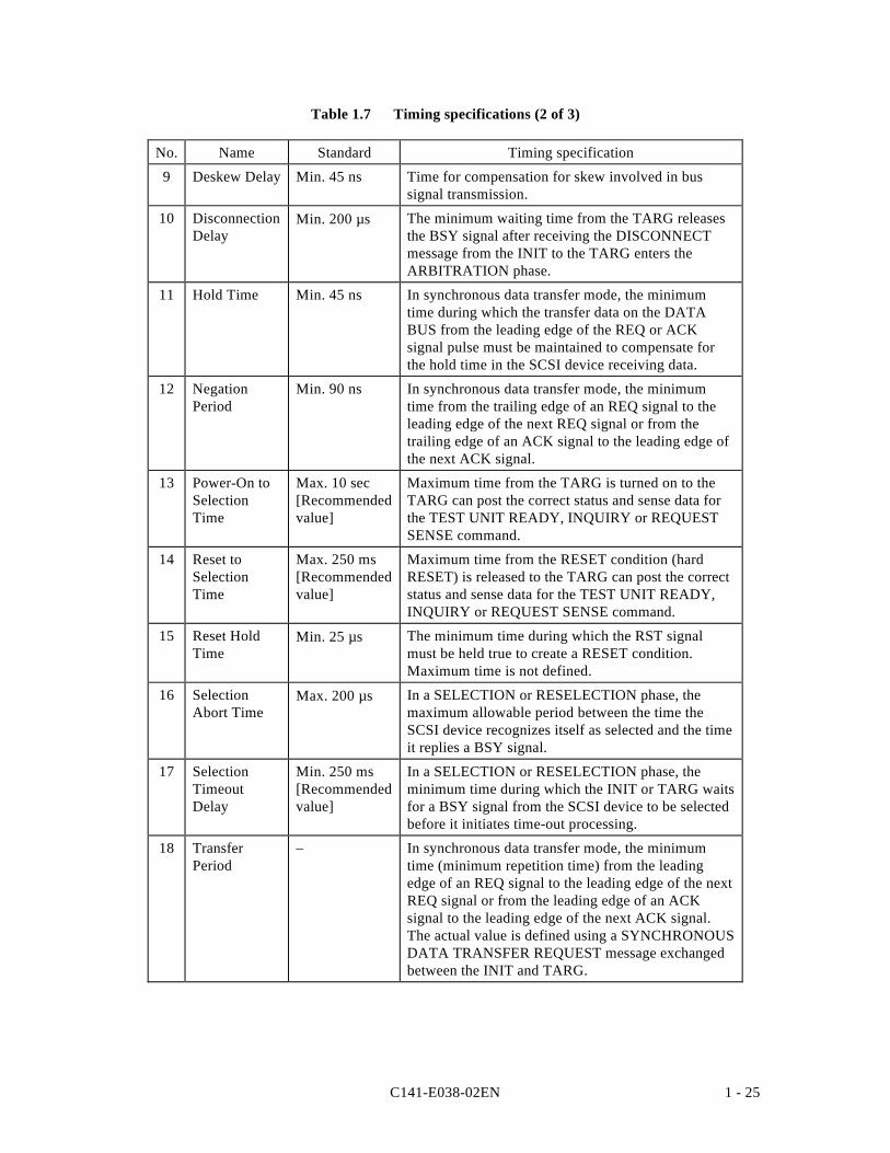
1.6.1 BUS FREE phase
All SCSI devices do not use the bus in the BUS FREE phase. SCSI devices shall detect theBUS FREE phase after SEL and SBY signals are both false for at least 400 ns (Bus SettleDelay).
SCSI devices which have detected the BUS FREE phase shall release all bus signals within800 ns (Bus Clear Delay) after BSY and SEL signals become false for 400 ns (Bus SettleDelay). If a SCSI device requires more than 400 ns (Bus Settle Delay) to detect the BUSFREE phase, it shall release all bus signals within the following period (t):
t = 800 ns (Bus Clear Delay) - (Period required for BUS FREE phase detection)+ 400 ns (Bus Settle Delay)
The maximum time allowed for releasing the bus after both SEL and BSY becomes false is1,200 ns (Bus Settle Delay + Bus Clear Delay).
Figure 1.16 shows the BUS FREE phase.
Figure 1.16 BUS FREE phase
C141-E038-02EN1 - 28
The SCSI bus enters the BUS FREE phase when the TARG stops the BSY signal in one of thefollowing events:
• When RESET condition has been detected
• When the TARG has received the ABORT message normally
• When the TARG has received the BUS DEVICE RESET message normally
• When the TARG has sent the DISCONNECT message normally
• When the TARG has sent the COMMAND COMPLETE message normally
• When the TARG has received the ABORT TAG message normally
• When the TARG has received the CLEAR QUEUE message normally
If a SELECTION or RESELECTION phase is terminated unsuccessfully, the SCSI bus enters theBUS FREE phase. This BUS FREE phase is generated when the SEL signal becomes false.
In any case other than above, if the TARG negates the BSY signal to enter a BUS FREEphase, the TARG informs the INIT that it has detected an ERROR condition of the SCSI bus.The TARG can enter a BUS FREE phase forcibly regardless of ATN signal status; the INITmust treat that phase transition as indicating the abnormal end of command. The TARG clearsall hold data or status and terminates the command being executed. It can then create sensedata indicating the detailed error condition. If the INIT detects a BUS FREE phase when it isnot expected, it should issue a REQUEST SENSE command to read the sense data.
1.6.2 ARBITRATION phase
The ARBITRATION phase allows one SCSI device to gain control of the SCSI bus. TheSCSI device that gets control of the SCSI bus can start the operation as INIT or TARG.
This is an optional system bus phase. This phase is required for the system that has two ormore INITs or uses the RESELECTION phase.
Figure 1.17 shows the ARBITRATION phase, and the following explains how the SCSIdevice gets control of the SCSI bus.
1) The SCSI device shall wait for BUS FREE phase. (see Section 1.6.1).
2) The SCSI device shall wait at least 800 ns (Bus Free Delay) after the BUS FREE phasedetection.
3) Then the SCSI device that arbitrates the bus asserts the DATA BUS bit corresponding toits own SCSI ID and BSY signal (*1) within 1.8 µs (Bus Set Delay) after last observationof the BUS FREE phase.
4) After waiting at least 2.4 µs (Arbitration Delay) since the SCSI device asserted BSYsignal, the SCSI device shall examine the value on the DATA BUS to determine thepriority of the bus arbitration (*1).
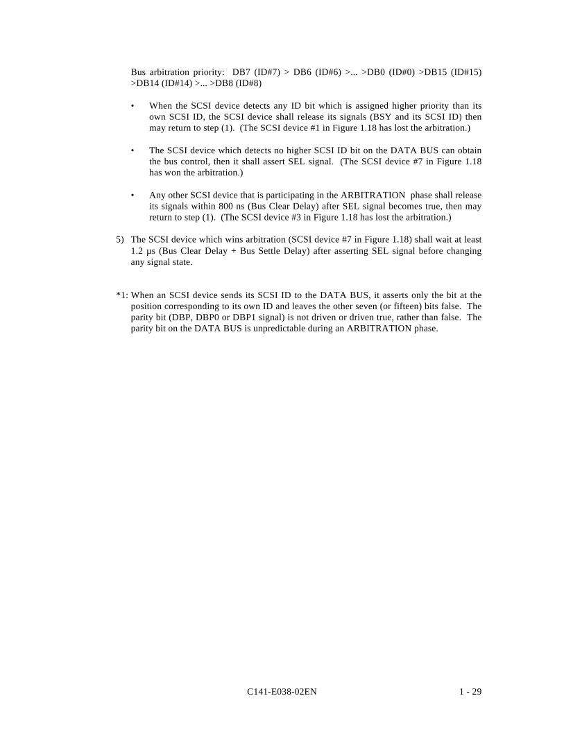
C141-E038-02EN 1 - 29
Bus arbitration priority: DB7 (ID#7) > DB6 (ID#6) >... >DB0 (ID#0) >DB15 (ID#15)>DB14 (ID#14) >... >DB8 (ID#8)
• When the SCSI device detects any ID bit which is assigned higher priority than itsown SCSI ID, the SCSI device shall release its signals (BSY and its SCSI ID) thenmay return to step (1). (The SCSI device #1 in Figure 1.18 has lost the arbitration.)
• The SCSI device which detects no higher SCSI ID bit on the DATA BUS can obtainthe bus control, then it shall assert SEL signal. (The SCSI device #7 in Figure 1.18has won the arbitration.)
• Any other SCSI device that is participating in the ARBITRATION phase shall releaseits signals within 800 ns (Bus Clear Delay) after SEL signal becomes true, then mayreturn to step (1). (The SCSI device #3 in Figure 1.18 has lost the arbitration.)
5) The SCSI device which wins arbitration (SCSI device #7 in Figure 1.18) shall wait at least1.2 µs (Bus Clear Delay + Bus Settle Delay) after asserting SEL signal before changingany signal state.
*1: When an SCSI device sends its SCSI ID to the DATA BUS, it asserts only the bit at theposition corresponding to its own ID and leaves the other seven (or fifteen) bits false. Theparity bit (DBP, DBP0 or DBP1 signal) is not driven or driven true, rather than false. Theparity bit on the DATA BUS is unpredictable during an ARBITRATION phase.
C141-E038-02EN1 - 30
Figure 1.17 ARBITRATION phase
C141-E038-02EN 1 - 31
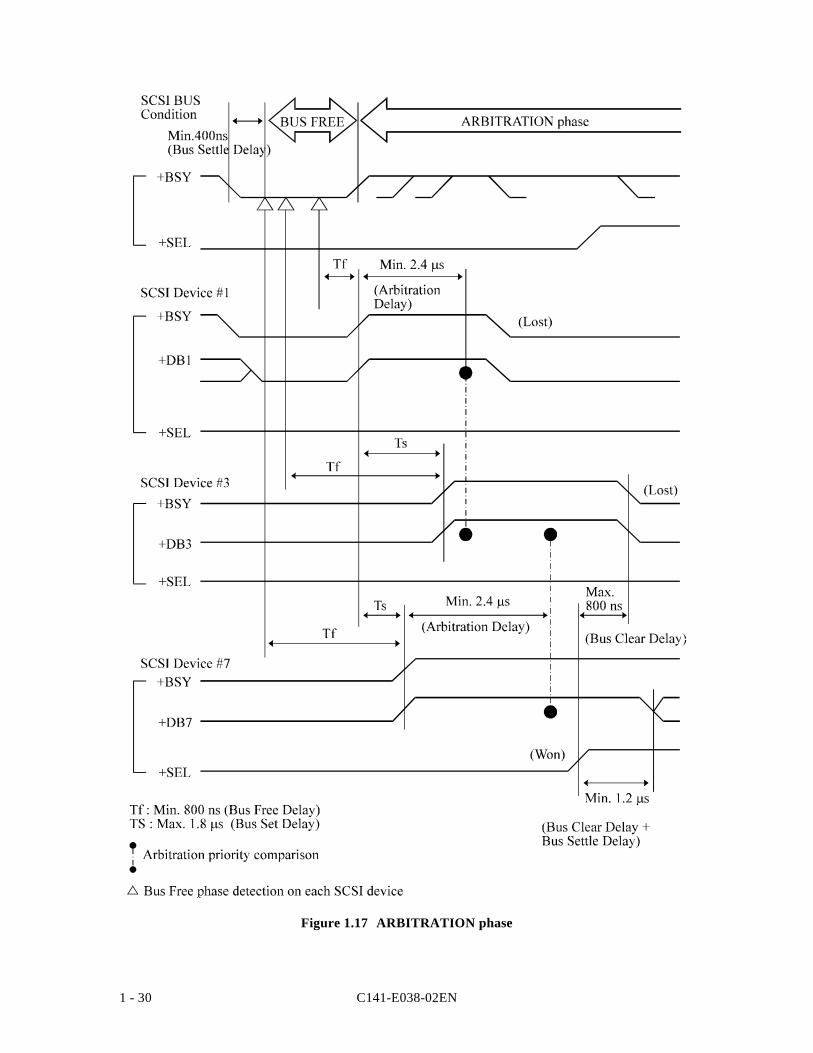
1.6.3 SELECTION phase
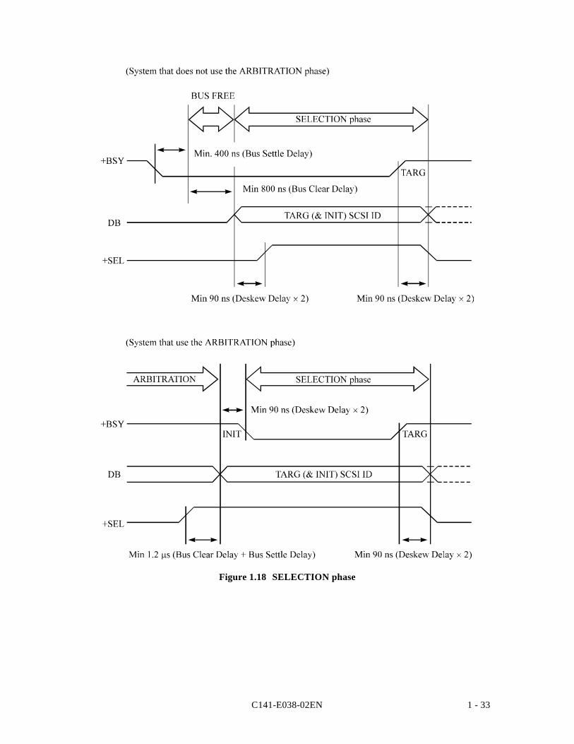
An INIT selects a TARG (a single SCSI unit) in the SELECTION phase.
Note:
I/O signal is false during a SELECTION phase. (The I/O signal identifies the phase asSELECTION or RESELECTION).
(1) Start sequence without ARBITRATION phase
In systems with the ARBITRATION phase not implemented, the INIT starts the SELECTIONphase in the following sequence (see Figure 1.18).
1) The INIT shall wait for at least 800 ns (Bus Clear Delay) after BUS FREE phase detection.
2) Then the INIT asserts SCSI IDs of desired TARG and INIT itself on the DATA BUS.
Note:
It single INIT operates without the RESELECTION phase, it is allowed to assert onlythe TARG's SCSI ID.
3) After waiting at least 90 ns (Deskew Delay × 2), the INIT asserts SEL signal and waits theresponse (BSY signal) from the TARG.
(2) Start sequence with ARBITRATION phase
In systems with ARBITRATION phase implemented, the INIT starts the SELECTION phasein the following sequence (see Figure 1.18).
1) The INIT shall wait for at least 1.2 µs (Bus Clear Delay + Bus Settle Delay) after turningSEL signal on during the ARBITRATION phase.
2) Then the INIT asserts SCSI IDs of the desired TARG and INIT itself on the DATA BUS.
Note:
If single INIT operates without RESELECTION phase, it is allowed to assert only theTARG's SCSI ID.
3) The INIT releases BSY signal after waiting at least 90 ns (Deskew Delay × 2). The INITshall then wait at least 400 ns (Bus Settle Delay) before looking for the response (BSYsignal) from the TARG.
C141-E038-02EN1 - 32
(3) Response sequence
When an SCSI device (TARG) detects that the SEL signal and the data bus bit (DBu)correponding to the own SCSI ID are true and both BSY and I/O signals are false for at least400 ns (Bus Settle Delay), the SCSI device shall recognize that it is selected in theSELECTION phase. At this time, the selected TARG may sample all bits on the SCSI bus toidentify the INIT's SCSI ID.
The TARG must response to the INIT by asserting the BSY signal within 200 µs (SelectionAbort Time) from the TARG detects that the TARG is selected. If the SCSI ID with three ormore bits is detected, or if a parity error is detected under the system that the parity bit isenabled, the TARG shall not respond to the SELECTION phase.
At least 90 ns (Deskew Delay × 2) after the BSY signal (asserted by the TARG) detection, theINIT shall release SEL signal. The values on the DATA BUS can be changed after this time.
(4) Timeout procedure
If the INIT cannot detect the response from TARG when the Selection Timeout Delay(recommended: 250 ms) or longer has passed after starting the SELECTION phase, thetimeout procedure shall be performed through one of the following schemes:
• The INIT asserts the RST signal and creates the RESET condition.
• The INIT maintains SEL signal true and stops sending SCSI ID to the data bus.Subsequently, the INIT waits for the response from TARG for at least 200 µs(SELECTION About Time) + 90 ns (Deskew Delay × 2). If no response is detected, theINIT releases the SEL signal allowing the SCSI bus to go to the BUS FREE phase. If theINIT detects the response from TARG during this period, the INIT considers theSELECTION phase to have completed normally.
C141-E038-02EN 1 - 33
Figure 1.18 SELECTION phase
C141-E038-02EN1 - 34
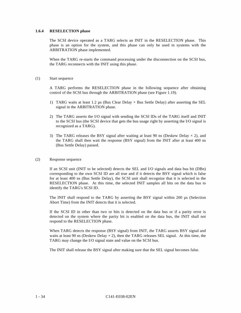
1.6.4 RESELECTION phase
The SCSI device operated as a TARG selects an INIT in the RESELECTION phase. Thisphase is an option for the system, and this phase can only be used in systems with theARBITRATION phase implemented.
When the TARG re-starts the command processing under the disconnection on the SCSI bus,the TARG reconnects with the INIT using this phase.
(1) Start sequence
A TARG performs the RESELECTION phase in the following sequence after obtainingcontrol of the SCSI bus through the ARBITRATION phase (see Figure 1.19).
1) TARG waits at least 1.2 µs (Bus Clear Delay + Bus Settle Delay) after asserting the SELsignal in the ARBITRATION phase.
2) The TARG asserts the I/O signal with sending the SCSI IDs of the TARG itself and INITto the SCSI bus (the SCSI device that gets the bus usage right by asserting the I/O signal isrecognized as a TARG).
3) The TARG releases the BSY signal after waiting at least 90 ns (Deskew Delay × 2), andthe TARG shall then wait the response (BSY signal) from the INIT after at least 400 ns(Bus Settle Delay) passed.
(2) Response sequence
If an SCSI unit (INIT to be selected) detects the SEL and I/O signals and data bus bit (DBn)corresponding to the own SCSI ID are all true and if it detects the BSY signal which is falsefor at least 400 ns (Bus Settle Delay), the SCSI unit shall recognize that it is selected in theRESELECTION phase. At this time, the selected INIT samples all bits on the data bus toidentify the TARG's SCSI ID.
The INIT shall respond to the TARG by asserting the BSY signal within 200 µs (SelectionAbort Time) from the INIT detects that it is selected.
If the SCSI ID in other than two or bits is detected on the data bus or if a parity error isdetected on the system where the parity bit is enabled on the data bus, the INIT shall notrespond to the RESELECTION phase.
When TARG detects the response (BSY signal) from INIT, the TARG asserts BSY signal andwaits at least 90 ns (Deskew Delay × 2), then the TARG releases SEL signal. At this time, theTARG may change the I/O signal state and value on the SCSI bus.
The INIT shall release the BSY signal after making sure that the SEL signal becomes false.
C141-E038-02EN 1 - 35
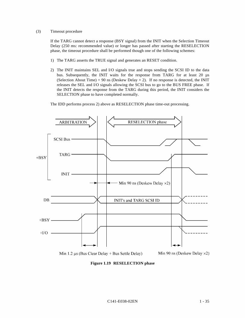
(3) Timeout procedure
If the TARG cannot detect a response (BSY signal) from the INIT when the Selection TimeoutDelay (250 ms: recommended value) or longer has passed after starting the RESELECTIONphase, the timeout procedure shall be performed though one of the following schemes:
1) The TARG asserts the TRUE signal and generates an RESET condition.
2) The INIT maintains SEL and I/O signals true and stops sending the SCSI ID to the databus. Subsequently, the INIT waits for the response from TARG for at least 20 µs(Selection About Time) + 90 ns (Deskew Delay × 2). If no response is detected, the INITreleases the SEL and I/O signals allowing the SCSI bus to go to the BUS FREE phase. Ifthe INIT detects the response from the TARG during this period, the INIT considers theSELECTION phase to have completed normally.
The IDD performs process 2) above as RESELECTION phase time-out processing.
Figure 1.19 RESELECTION phase
C141-E038-02EN1 - 36
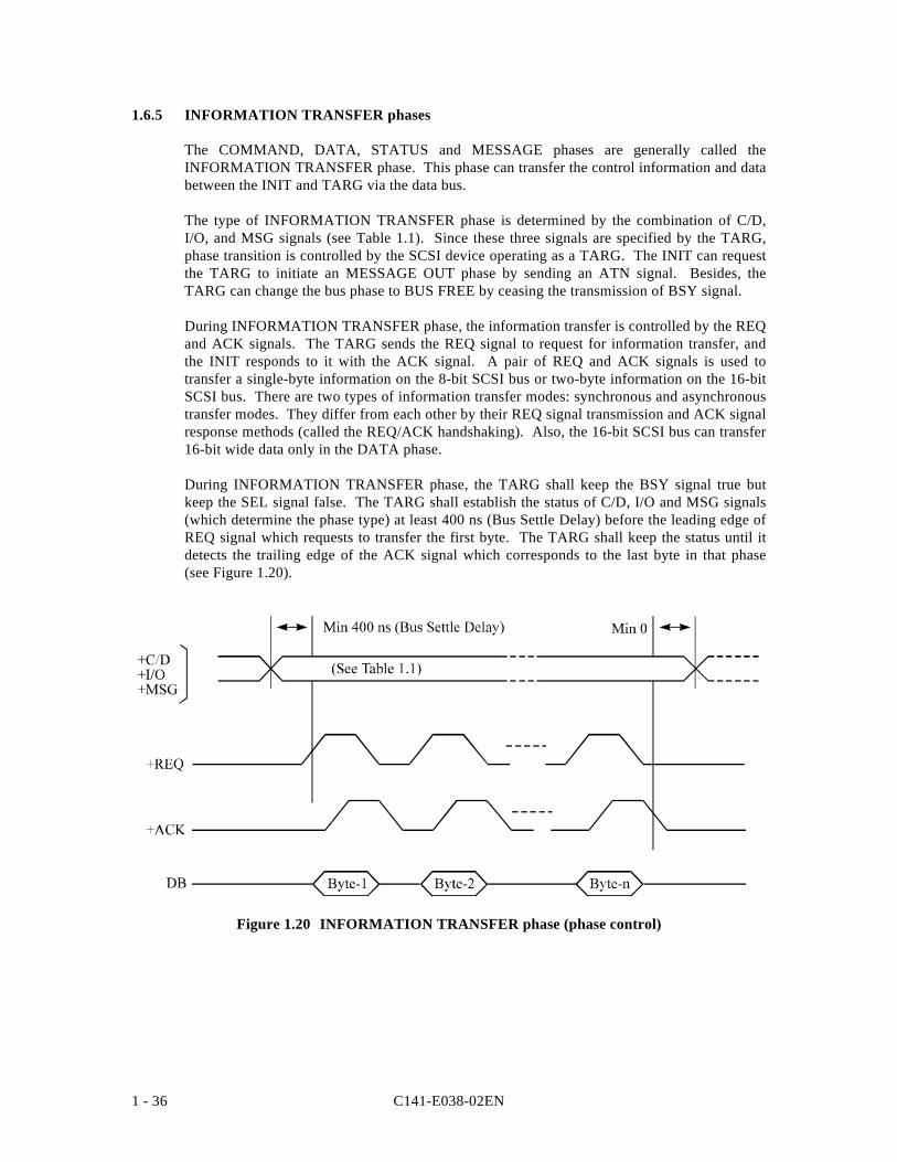
1.6.5 INFORMATION TRANSFER phases
The COMMAND, DATA, STATUS and MESSAGE phases are generally called theINFORMATION TRANSFER phase. This phase can transfer the control information and databetween the INIT and TARG via the data bus.
The type of INFORMATION TRANSFER phase is determined by the combination of C/D,I/O, and MSG signals (see Table 1.1). Since these three signals are specified by the TARG,phase transition is controlled by the SCSI device operating as a TARG. The INIT can requestthe TARG to initiate an MESSAGE OUT phase by sending an ATN signal. Besides, theTARG can change the bus phase to BUS FREE by ceasing the transmission of BSY signal.
During INFORMATION TRANSFER phase, the information transfer is controlled by the REQand ACK signals. The TARG sends the REQ signal to request for information transfer, andthe INIT responds to it with the ACK signal. A pair of REQ and ACK signals is used totransfer a single-byte information on the 8-bit SCSI bus or two-byte information on the 16-bitSCSI bus. There are two types of information transfer modes: synchronous and asynchronoustransfer modes. They differ from each other by their REQ signal transmission and ACK signalresponse methods (called the REQ/ACK handshaking). Also, the 16-bit SCSI bus can transfer16-bit wide data only in the DATA phase.
During INFORMATION TRANSFER phase, the TARG shall keep the BSY signal true butkeep the SEL signal false. The TARG shall establish the status of C/D, I/O and MSG signals(which determine the phase type) at least 400 ns (Bus Settle Delay) before the leading edge ofREQ signal which requests to transfer the first byte. The TARG shall keep the status until itdetects the trailing edge of the ACK signal which corresponds to the last byte in that phase(see Figure 1.20).
Figure 1.20 INFORMATION TRANSFER phase (phase control)
C141-E038-02EN 1 - 37
Notes:
1. After the ACK signal becomes false in the current INFORMATION TRANSFERphase, the TARG can start preparing a new phase by changing the status of C/D, I/Oand MSG signals. The status of these three signals can change in any order or atonce. The status of one signal may change more than once; however, the TARGshould change the status of each signal only once.
2. A new INFORMATION TRANSFER phase starts when the REQ signal requesting totransfer the first byte in that phase becomes true. The phase ends when one of C/D,I/O and MSG signals changes after the ACK signal has changed to false. The periodafter the end of phase to the start of next phase (which starts when the REQ signalbecomes true) is not defined.
3. The INIT can predict the next new phase (expected phase) by reading the statuschange of C/D, I/O or MSG signal or by reading the type of previously executedphase. However, the expected phase is made valid only when the REQ signal ischanged to true.
(1) Asynchronous transfer mode
In asynchronous transfer mode, the INIT and TARG control the information transfer bychecking the status change of REQ and ACK signals (between true and false state) by eachother (it is called the interlock control). The asynchronous transfer can be used in all types ofINFORMATION TRANSFER phase (such as COMMAND, DATA, STATUS andMESSAGE). Figure 1.21 shows the timing of asynchronous transfer.
If the wide mode data transfer is established between the INIT and TARG, the two-byte data(DB15 to DB0, DBP1, DBP0) is transferred on the 16-bit SCSI bus. Otherwise, single-bytedata (DB7 to DB0, DBP) is transferred.
a. Transfer from TARG to INIT
The TARG determines the information transfer direction by the I/O signal. If the I/Osignal is true, the information of the data bus is transferred from the TARG to the INIT.The following explains the information transfer sequence.
1) The TARG asserts the REQ signal at least 55 ns (Deskew Delay + Cable Skew Delay)after sending valid information on the data bus. It must maintain the state of the databus until the ACK signal becomes true on the TARG.
2) The INIT fetches the data from the data bus after the REQ signal becomes true. Itasserts the ACK signal to report the completion of reception.
3) After the ACK signal becomes true on the TARG, the TARG negates the REQ signal.Thereafter, the TARG can change the data of the data bus.
4) The INIT negates the ACK signal after the REQ signal becomes false.
5) After the ACK signal becomes false, the TARG proceeds to the next byte transferstage.
C141-E038-02EN1 - 38
b. Transfer from INIT to TARG
When the I/O signal is false, the information of the data bus is transferred from the INIT tothe TARG. The following explains the information transfer sequence.
1) The TARG asserts the REQ signal to request the INIT for information transfer.
2) The INIT asserts the ACK signal at least 55 ns (Deskew Delay + Cable Skew Delay)after sending valid information of the requested type on the data bus. Theinformation on the data bus must be maintained until the REQ signal becomes falseon the INIT.
3) The TARG fetches data from the data bus after the ACK signal becomes true, andnegates the REQ signal to report the completion of reception.
4) When the REQ signal becomes false on the INIT, the INIT negates the ACK signal.After that, the INIT can change data on the data bus.
5) After the ACK signal becomes false, the TARG proceeds to the next byte transferstage.
C141-E038-02EN 1 - 39
Figure 1.21 Transfer in asynchronous mode
C141-E038-02EN1 - 40
(2) Synchronous mode
The synchronous transfer mode allows information transfer with REQ and ACK signal check bytheir pulse count (called the offset interlock). This mode can be used in the DATA phase only.
Note:
1. The IDD supports up to 10 MB/s of synchronous data transfer. The "Fast SCSI" parametershall be used for 5 MB/s or higher synchronous data transfer (see Table 1.7).
2. The default data transfer mode is asynchronous. When the power is first turned on,the system is reset, or after the BUS DEVICE RESET message has been issued, datais transferred in the asynchronous mode only. It continues until the synchronoustransfer mode is selected by the message exchange explained below.
The synchronous data transfer is available only when it has been defined between the INIT andTARG by exchanging the SYNCHRONOUS DATA TRANSFER REQUEST message witheach other. The following data transfer parameters are determined and the possible transferrate between the SCSI units are defined by this message exchange.
• REQ/ACK Offset: Number of REQ signals that the TARG can send before receiving theACK signal.
• Transfer Period: Minimum repetition cycle of REQ and ACK signals.
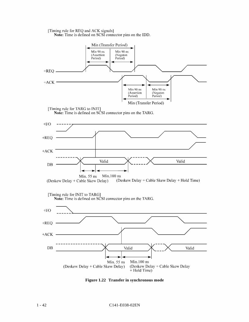
When the SCSI devices negotiate a transfer period of less than 200 ns, they are said to be using"Fast Synchronous Transfer (Fast SCSI)". The minimum synchronous data transfer period is 100 ns.
The TARG can send multiple REQ signal pulses before receiving an ACK signal response ifthese pulses do not exceed the limit specified by the REQ/ACK Offset parameter. When thedifference between the REQ and ACK signal pulses has reached this limit at the TARG, theTARG shall not send a REQ pulse until it receives the leading edge of the next ACK pulse.The data transfer in DATA phase can complete normally only when the REQ and ACK signalpulses become equal to each other.
The TARG shall satisfy the following time requirements at its SCSI connector pins duringREQ signal transfer.
• Minimum pulse width is 90 ns (Assertion Period) or 30 ns (Fast Assertion Period).
• Minimum period from the trailing edge of a pulse to the leading edge of the next pulse is90 ns (Negation Period) or 30 ns (Fast Negation Period).
• Period between the leading edges of a pulse and the next pulse is equal to or greater thanthe time defined by the Transfer Period parameter.
When receiving REQ pulses from the TARG, the INIT must respond to it with the samenumber of ACK pulses. The INIT can send the ACK signal just when it receives the leadingedge of corresponding REQ signal. The INIT shall satisfy the following time requirements atits SCSI connectors when sending ACK signals:
C141-E038-02EN 1 - 41
• Minimum pulse width is 90 ns (Assertion Period) or 30 ns (Fast Assertion Period).
• Minimum period between the trailing edge of a pulse and the leading edge of the nextpulse is 90 ns (Assertion Period) or 30 ns (Fast Assertion Period).
• Period between the leading edges of a pulse and the next pulse is equal to or greater thanthe time defined by the Transfer Period parameter.
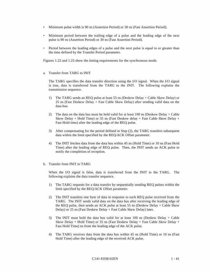
Figures 1.22 and 1.23 show the timing requirements for the synchronous mode.
a. Transfer from TARG to INIT
The TARG specifies the data transfer direction using the I/O signal. When the I/O signalis true, data is transferred from the TARG to the INIT. The following explains thetransmission sequence.
1) The TARG sends an REQ pulse at least 55 ns (Deskew Delay + Cable Skew Delay) or25 ns (Fast Deskew Delay + Fast Cable Skew Delay) after sending valid data on thedata bus.
2) The data on the data bus must be held valid for at least 100 ns (Deskew Delay + CableSkew Delay + Hold Time) or 35 ns (Fast Deskew delay + Fast Cable Skew Delay +Fast Hold time) after the leading edge of the REQ pulse.
3) After compensating for the period defined in Step (2), the TARG transfers subsequentdata within the limit specified by the REQ/ACK Offset parameter.
4) The INIT fetches data from the data bus within 45 ns (Hold Time) or 10 ns (Fast HoldTime) after the leading edge of REQ pulse. Then, the INIT sends an ACK pulse tonotify the completion of reception.
b. Transfer from INIT to TARG
When the I/O signal is false, data is transferred from the INIT to the TARG. Thefollowing explains the data transfer sequence.
1) The TARG requests for a data transfer by sequentially sending REQ pulses within thelimit specified by the REQ/ACK Offset parameter.
2) The INIT transfers one byte of data in response to each REQ pulse received from theTARG. The INIT sends valid data on the data bus after receiving the leading edge ofthe REQ pulse, then sends an ACK pulse at least 55 ns (Deskew Delay + Cable SkewDelay) or 25 ns (Fast Deskew Delay + Fast Cable Skew Delay) later.
3) The INIT must hold the data bus valid for at least 100 ns (Deskew Delay + CableSkew Delay + Hold Time) or 35 ns (Fast Deskew Delay + Fast Cable Skew Delay +Fast Hold Time) ns from the leading edge of the ACK pulse.
4) The TARG receives data from the data bus within 45 ns (Hold Time) or 10 ns (FastHold Time) after the leading edge of the received ACK pulse.
C141-E038-02EN1 - 42
Figure 1.22 Transfer in synchronous mode
C141-E038-02EN 1 - 43
Figure 1.23 Transfer in Fast synchronous mode
C141-E038-02EN1 - 44
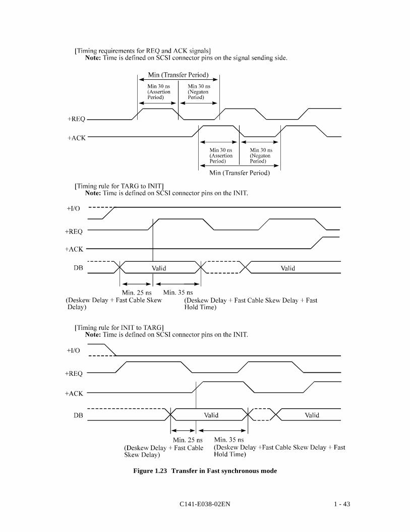
(3) Wide mode transfer (16-bit SCSI)
The wide mode transfer enables information transfer using a multiple-byte-wide data bus. It isused only in DATA phases.
In wide mode transfer, the WIDE DATA TRANSFER REQUEST message should first beexchanged by the INIT and the TARG to define the data transfer mode between SCSI devices.When the WIDE DATA TRANSFER REQUEST message is exchanged, a data bus width isdetermined. Figure 1.24 shows the data sequence at data transfer.
Note:
The IDD supports 8-bit and 16-bit transfer modes. The initial value of the data bus widthis "8-bit mode". After power is turned on, a RESET condition occurs, or a BUS DEVICEREQUEST message is received, data is transferred using 8-bit mode until the mode isswitched to "16-bit mode" by exchanging the WIDE DATA TRANSFER REQUESTmessage.
Number of informationitems transferred
P cable
1 Unused A “8-bit mode”
2 Unused B
DB15..............DB18 DB7..................DB0
1 B A “16-bit mode”
Figure 1.24 Data sequence at data transfer
1.6.6 COMMAND phase
The COMMAND phase is a bus phase in which the TARG requests the INIT to transfercommand information (CDB) to the TARG. The TARG keeps the C/D signal true and the I/Oand MSG signals false during REQ/ACK handshaking in this phase.
1.6.7 DATA phase
The DATA phase is divided into DATA IN and DATA OUT phases according to the directionof data transfer. In a DATA phase, synchronous data transfer can be performed.
(1) DATA IN phase
In a DATA IN phase, the TARG requests to transfer data from the TARG to the INIT. TheTARG keeps the I/O signal true and the C/D and MSG signals false during REQ/ACKhandshaking in this phase.
C141-E038-02EN 1 - 45
(2) DATA OUT phase
In a DATA OUT phase, the TARG requests to transfer data from the INIT to the TARG. TheTARG keeps the C/D, I/O, and MSG signals false during REQ/ACK handshaking in thisphase.
(3) Data transfer rate in asynchronous mode
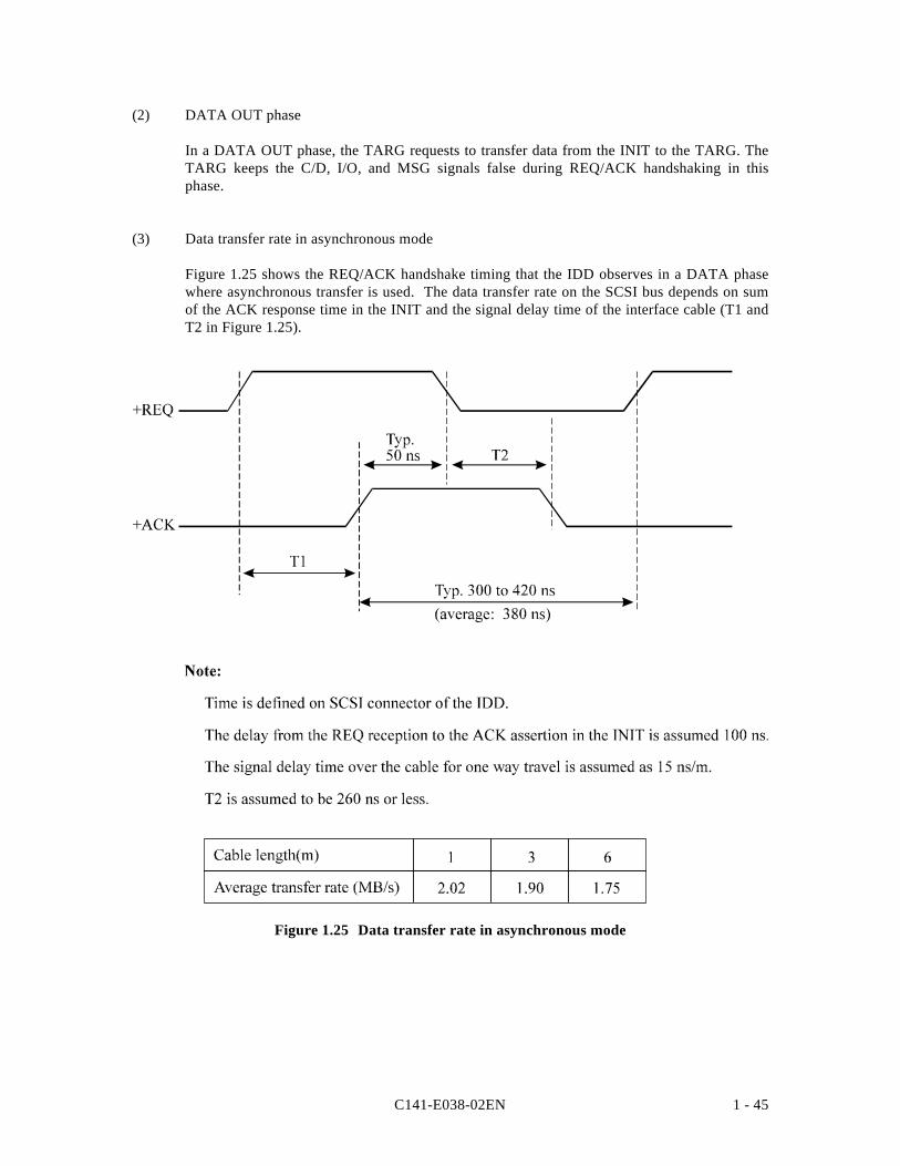
Figure 1.25 shows the REQ/ACK handshake timing that the IDD observes in a DATA phasewhere asynchronous transfer is used. The data transfer rate on the SCSI bus depends on sumof the ACK response time in the INIT and the signal delay time of the interface cable (T1 andT2 in Figure 1.25).
Figure 1.25 Data transfer rate in asynchronous mode
C141-E038-02EN1 - 46
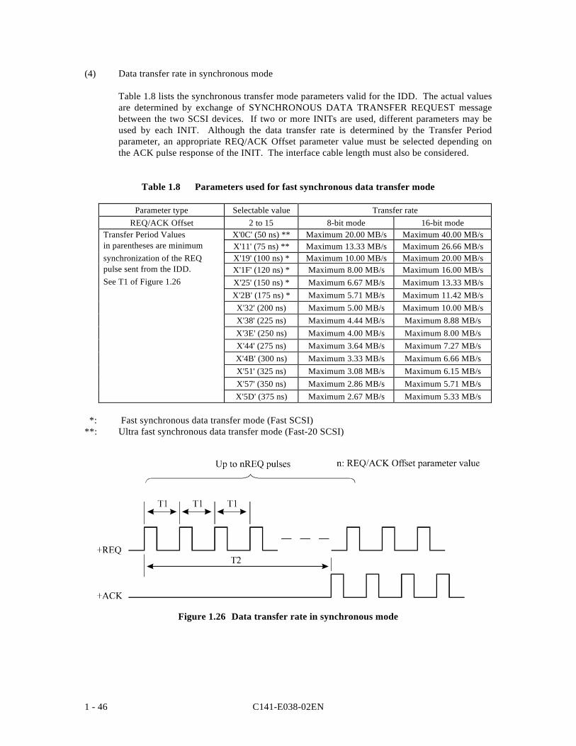
(4) Data transfer rate in synchronous mode
Table 1.8 lists the synchronous transfer mode parameters valid for the IDD. The actual valuesare determined by exchange of SYNCHRONOUS DATA TRANSFER REQUEST messagebetween the two SCSI devices. If two or more INITs are used, different parameters may beused by each INIT. Although the data transfer rate is determined by the Transfer Periodparameter, an appropriate REQ/ACK Offset parameter value must be selected depending onthe ACK pulse response of the INIT. The interface cable length must also be considered.
Table 1.8 Parameters used for fast synchronous data transfer mode
Parameter type Selectable value Transfer rateREQ/ACK Offset 2 to 15 8-bit mode 16-bit mode
Transfer Period Values X'0C' (50 ns) ** Maximum 20.00 MB/s Maximum 40.00 MB/sin parentheses are minimum X'11' (75 ns) ** Maximum 13.33 MB/s Maximum 26.66 MB/ssynchronization of the REQ X'19' (100 ns) * Maximum 10.00 MB/s Maximum 20.00 MB/spulse sent from the IDD. X'1F' (120 ns) * Maximum 8.00 MB/s Maximum 16.00 MB/sSee T1 of Figure 1.26 X'25' (150 ns) * Maximum 6.67 MB/s Maximum 13.33 MB/s
X'2B' (175 ns) * Maximum 5.71 MB/s Maximum 11.42 MB/sX'32' (200 ns) Maximum 5.00 MB/s Maximum 10.00 MB/sX'38' (225 ns) Maximum 4.44 MB/s Maximum 8.88 MB/sX'3E' (250 ns) Maximum 4.00 MB/s Maximum 8.00 MB/sX'44' (275 ns) Maximum 3.64 MB/s Maximum 7.27 MB/sX'4B' (300 ns) Maximum 3.33 MB/s Maximum 6.66 MB/sX'51' (325 ns) Maximum 3.08 MB/s Maximum 6.15 MB/sX'57' (350 ns) Maximum 2.86 MB/s Maximum 5.71 MB/sX'5D' (375 ns) Maximum 2.67 MB/s Maximum 5.33 MB/s
*: Fast synchronous data transfer mode (Fast SCSI)**: Ultra fast synchronous data transfer mode (Fast-20 SCSI)
Figure 1.26 Data transfer rate in synchronous mode
C141-E038-02EN 1 - 47
1.6.8 STATUS phase
In a STATUS phase, the TARG requests to transfer status information from the TARG to theINIT. The TARG keeps the C/D and I/O signals true and the MSG signal false duringREQ/ACK handshaking in this phase.
1.6.9 MESSAGE phase
The MESSAGE phase is divided into MESSAGE IN and MESSAGE OUT phases dependingon the direction of message information transfer. In either phase, several messages can betransferred.
The first byte transferred in a MESSAGE phase must be a single-byte message or the first byteof a multiple-byte message. If the message consists of more than one byte, all bytes must betransferred in a single MESSAGE phase. For details of message types and their operation,refer to Chapter 2.
(1) MESSAGE IN phase
In a MESSAGE IN phase, the TARG requests to transfer message information from the TARGto the INIT. The TARG keeps the C/D, I/O, and MSG signals true during REQ/ACKhandshaking in this phase.
(2) MESSAGE OUT phase
In a MESSAGE OUT phase, the TARG requests to transfer message information from theINIT to the TARG. The TARG keeps the C/D and MSG signals true and I/O signal falseduring REQ/ACK handshaking in this phase.
The TARG executes this phase in response to the ATTENTION condition (described inSection 1.7.1) created by the INIT, and must remain in the MESSAGE OUT phase.
Note:
The TARG can terminate the MESSAGE OUT phase even when the ATN signal is truewhen it returns a MESSAGE REJECT message to reject an illegal or invalid message,when it enters the BUS FREE phase as directed by the received message, or when itreturns a message immediately in response to a received message (such as theSYNCHRONOUS DATA TRANSFER REQUEST).
The TARG can process a received message immediately if no parity error is detected. If aparity error is detected, the TARG shall ignore all messages which have been received after theparity error detected in the MESSAGE OUT phase.
C141-E038-02EN1 - 48
When the TARG receives all message information correctly without detecting a parity error,the TARG shall enter the INFORMATION TRANSFER phase other than the MESSAGE OUTphase and execute at least one byte of information transfer in order to request the INIT not toretry message transfer. During some message transfer, the TARG may report the normalcompletion of message reception by switching to the BUS FREE phase (for example, ABORTand BUS DEVICE RESET messages).
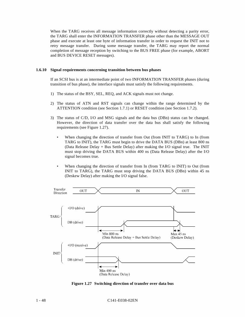
1.6.10 Signal requirements concerning transition between bus phases
If an SCSI bus is at an intermediate point of two INFORMATION TRANSFER phases (duringtransition of bus phase), the interface signals must satisfy the following requirements.
1) The status of the BSY, SEL, REQ, and ACK signals must not change.
2) The status of ATN and RST signals can change within the range determined by theATTENTION condition (see Section 1.7.1) or RESET condition (see Section 1.7.2).
3) The status of C/D, I/O and MSG signals and the data bus (DBn) status can be changed.However, the direction of data transfer over the data bus shall satisfy the followingrequirements (see Figure 1.27).
• When changing the direction of transfer from Out (from INIT to TARG) to In (fromTARG to INIT), the TARG must begin to drive the DATA BUS (DBn) at least 800 ns(Data Release Delay + Bus Settle Delay) after making the I/O signal true. The INITmust stop driving the DATA BUS within 400 ns (Data Release Delay) after the I/Osignal becomes true.
• When changing the direction of transfer from In (from TARG to INIT) to Out (fromINIT to TARG), the TARG must stop driving the DATA BUS (DBn) within 45 ns(Deskew Delay) after making the I/O signal false.
Figure 1.27 Switching direction of transfer over data bus
C141-E038-02EN 1 - 49
1.6.11 Time monitoring feature
The IDD has a time monitoring feature for the SCSI bus to prevent the hang-up of the SCSIbus in the case that the IDD cannot receive a response from the INIT in the RESELECTIONphase.
The IDD monitors the response from the INIT (BSY signal) in the RESELECTION phase.When the IDD cannot receive the response within a specified period (250 ms), the IDDexecutes the timeout process (see Section 1.6.4) and releases the SCSI bus once. After that theIDD executes the retry process of the RESELECTION phase (see Section 3.1).
The user can select the number of retries of the RESELECTION phase by the CHANGEDEFINITION command.
Table 1.9 Retry count setting for RESELECTION phase
RSRTY bit Retry count forRESELECTION phase
"0" 10 times
"1" (Setting at shipping) ∞ (Unlimited)
For details on setting, refer to Subsection 3.1.4, in the SCSI Logical Interface Specifications.
C141-E038-02EN1 - 50
1.7 Bus Conditions
Two types of asynchronous control, the ATTENTION condition and RESET condition, shallbe defined to control or modify the bus phase transition sequence (bus conditions).
1.7.1 ATTENTION condition
The ATTENTION condition allows the INIT to report that the INIT has a message to be sentto the TARG. The TARG receives the message from the INIT by starting the MESSAGEOUT phase. Figure 1.28 shows the ATTENTION condition.
(1) Generation and release of ATTENTION condition (INIT)
The INIT can generate the ATTENTION condition by asserting the ATN signal except for theARBITRATION or BUS FREE phase.
When generating of a new ATTENTION condition in the INFORMATION TRANSFERphase, to inform the TARG of the ATTENTION condition before the transition to the nextnew bus phase, the INIT must set the ATN signal true before 90 ns (Deskew Delay × 2) ormore from the timing of setting false the ACK signal for the last byte being transferred in thecurrent bus phase. If the ATN sending timing is delayed, the TARG may not be informed ofthe ATTENTION condition until the next bus phase. The INIT may not operate as it should.
When transferring message information in several bytes in the MESSAGE OUT phase, theINIT must keep the ATN signal true. The INIT can make the ATN signal false any timeexcept while the ACK signal is true in the MESSAGE OUT phase. When transferring the lastbyte in the MESSAGE OUT phase, the INIT generally makes the ATN signal false during theperiod between the time the REQ signal becomes true and the time it replies the ACK signal.In this case, the INIT must set the ATN signal false before 90 ns (Deskew Delay × 2) or moreform the timing of setting true the ACK signal.
The INIT must make the ATN signal false before making the ACK signal true to transfer the lastmessage byte if so specified for the particular type of message to the TARG. (See Subsection 2.1.2.)
(2) Response against ATTENTION condition (TARG)
The TARG shall start the MESSAGE OUT phase and respond to the ATTENTION conditionin the following conditions. Also, the TARG shall enter the MESSAGE OUT phase when theATN signal is true after the TARG returns the MESSAGE REJECT or other message withhalting the MESSAGE OUT phase.
• When the ATN signal becomes true in the COMMAND phase, the TARG shall start theMESSAGE OUT phase immediately after a part or all bytes of command (CDB) has beentransferred.
• When the ATN signal becomes true in the DATA phase, the TARG shall start theMESSAGE OUT phase immediately after the DATA phase. However, the TARG canenter the MESSAGE OUT phase any time when necessary. (Data transfer is notinterrupted on a boundary of logical data blocks.) The INIT shall continue the REQ/ACKhandshaking (in DATA phase) until the bus phase is changed.
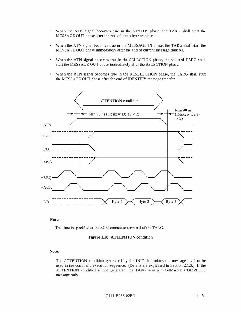
C141-E038-02EN 1 - 51
• When the ATN signal becomes true in the STATUS phase, the TARG shall start theMESSAGE OUT phase after the end of status byte transfer.
• When the ATN signal becomes true in the MESSAGE IN phase, the TARG shall start theMESSAGE OUT phase immediately after the end of current message transfer.
• When the ATN signal becomes true in the SELECTION phase, the selected TARG shallstart the MESSAGE OUT phase immediately after the SELECTION phase.
• When the ATN signal becomes true in the RESELECTION phase, the TARG shall startthe MESSAGE OUT phase after the end of IDENTIFY message transfer.
Figure 1.28 ATTENTION condition
Note:
The ATTENTION condition generated by the INIT determines the message level to beused in the command execution sequence. (Details are explained in Section 2.1.3.) If theATTENTION condition is not generated, the TARG uses a COMMAND COMPLETEmessage only.
C141-E038-02EN1 - 52
1.7.2 RESET condition
The RESET condition allows all SCSI devices to release immediately from the bus. RESEThas higher priority than any other phases and bus conditions. Any SCSI device can generatethe RESET condition anytime by keeping the RST signal true for 25 µs (Reset Hold Time) ormore. The state of all bus signals except RST signals are undefined during the RESETcondition.
All SCSI devices shall stop driving all bus signals (except for the RST signal) and release thebus within 800 ns (Bus Clear Delay) after the RST signal becomes true. After the RESETcondition, the SCSI bus always enters the BUS FREE phase. Figure 1.29 shows the RESETcondition.
The following are the IDD operations when the RESET condition is detected.
1) Clears all commands including the currently executing commands and queued commands.
2) Releases the reserved disk state of the disk drive.
3) Initializes the operation mode to its initial status just after power-on if it has been set bythe message or command.
• The current value of the parameter set by the MODE SELECT command is initializedto the saved value previously established. If the value is not saved, it is initialized tothe default value.
• The synchronous transfer parameters defined between the IDD and other SCSI deviceare cleared. Any data transfer mode between all SCSI devices is initialized to theasynchronous mode.
4) The UNIT ATTENTION condition is generated for all SCSI devices.
5) The sense data is no longer retained and is cleared.
6) All data read into the data buffer in advance by the read-ahead cache feature is invalidated.
Notes:
1. The IDD does not generate a RESET condition.
2. The IDD provides only "hard" RESET condition specified by the SCSI standard.
3. Reset Hold Time (min. 25 µs) is specified to guarantee that any SCSI device canrecognize the occurrence the RESET condition. On the IDD, even if the pulse widthis less than 25 µs, the RESET condition is effective.
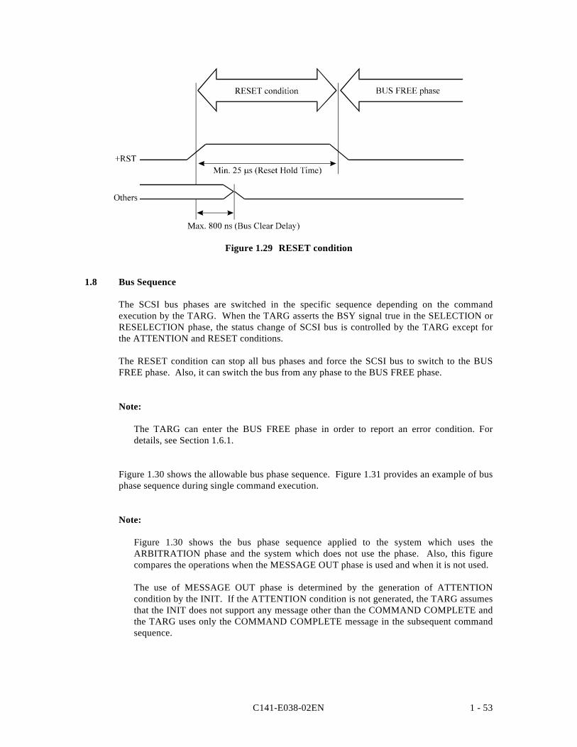
C141-E038-02EN 1 - 53
Figure 1.29 RESET condition
1.8 Bus Sequence
The SCSI bus phases are switched in the specific sequence depending on the commandexecution by the TARG. When the TARG asserts the BSY signal true in the SELECTION orRESELECTION phase, the status change of SCSI bus is controlled by the TARG except forthe ATTENTION and RESET conditions.
The RESET condition can stop all bus phases and force the SCSI bus to switch to the BUSFREE phase. Also, it can switch the bus from any phase to the BUS FREE phase.
Note:
The TARG can enter the BUS FREE phase in order to report an error condition. Fordetails, see Section 1.6.1.
Figure 1.30 shows the allowable bus phase sequence. Figure 1.31 provides an example of busphase sequence during single command execution.
Note:
Figure 1.30 shows the bus phase sequence applied to the system which uses theARBITRATION phase and the system which does not use the phase. Also, this figurecompares the operations when the MESSAGE OUT phase is used and when it is not used.
The use of MESSAGE OUT phase is determined by the generation of ATTENTIONcondition by the INIT. If the ATTENTION condition is not generated, the TARG assumesthat the INIT does not support any message other than the COMMAND COMPLETE andthe TARG uses only the COMMAND COMPLETE message in the subsequent commandsequence.
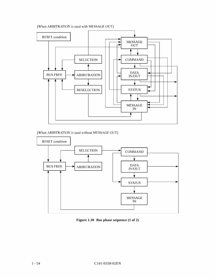
C141-E038-02EN1 - 54
Figure 1.30 Bus phase sequence (1 of 2)
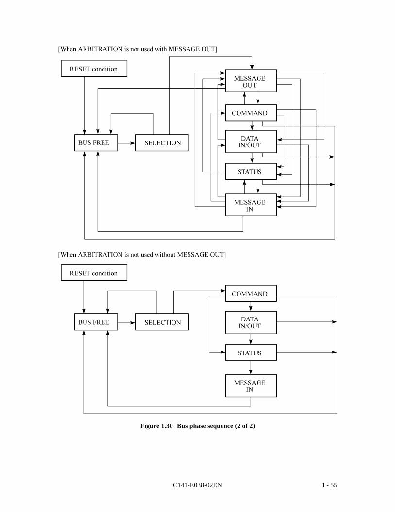
C141-E038-02EN 1 - 55
Figure 1.30 Bus phase sequence (2 of 2)
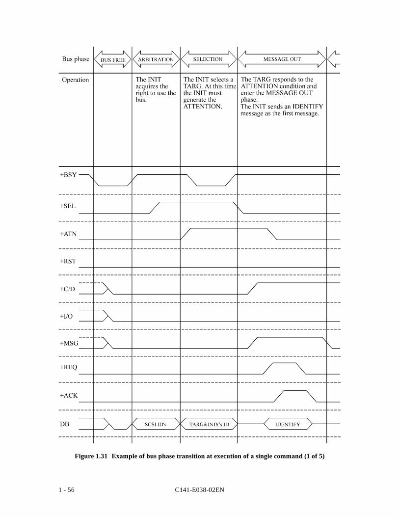
C141-E038-02EN1 - 56
Figure 1.31 Example of bus phase transition at execution of a single command (1 of 5)
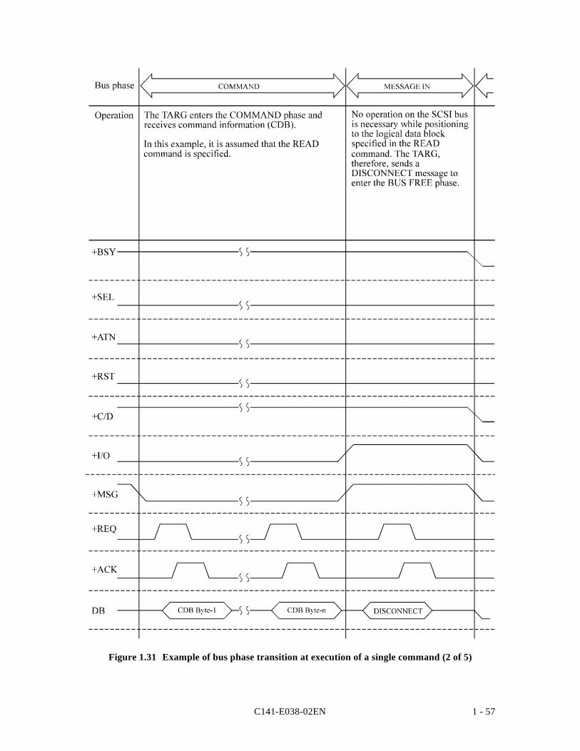
C141-E038-02EN 1 - 57
Figure 1.31 Example of bus phase transition at execution of a single command (2 of 5)
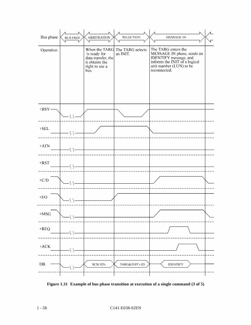
C141-E038-02EN1 - 58
Figure 1.31 Example of bus phase transition at execution of a single command (3 of 5)
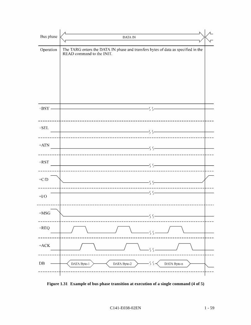
C141-E038-02EN 1 - 59
Figure 1.31 Example of bus phase transition at execution of a single command (4 of 5)
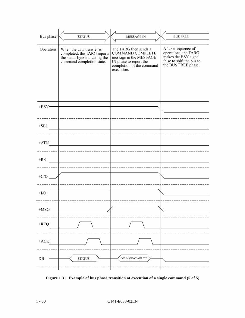
C141-E038-02EN1 - 60
Figure 1.31 Example of bus phase transition at execution of a single command (5 of 5)
C141-E038-02EN 1 - 61
1.9 SCAM
The IDD supports the level-1 SCAM only.
1.9.1 SCAM operations
The SCAM operation functions include all functions required for ID assignment of eachSCAM device so that the SCAM tolerant and SCAM devices are identified by the SCAMinitiator and target. The user shall understand the SCAM operations clearly by knowing theoperations between the SCAM initiator and target.
(1) SCAM initiator
The SCAM initiator shall complete its local initialization immediately after the power-on. Itshall wait during the delay from the SCAM power-on to the SCAM selection. The SCAMinitiator, which can be a level-1 SCAM device or can be determined to be the dominantSCAM initiator, shall generate a RESET condition immediately after power-on. The level-2SCAM initiator, which cannot be determined to be the dominant SCAM initiator by thedeductive method, shall not generate a RESET condition. However, it shall start the SCAMprotocol as if it has detected the RESET condition as described below.
When the SCAM initiator generates or detects a RESET condition, it shall start the SCAMprotocol. The first function sequence shall be the Dominant Initiator Contention function.The SCAM initiator becomes the dominant SCAM initiator when it broadcasts the numericallyhighest ID character string during separation. The SCAM initiator which does not have thehighest ID character string is set to a subaudinate SCAM initiator.
Notes:
The level-1 SCAM initiator is not always required for execution of the Dominant InitiatorContention function. It shall be used to detect the Dominant Initiator Contention functionwhich is broadcasted by another SCAM initiator.
The ID character string of the level-1 SCAM initiator has been defined not to be selectedthrough contention by the level-2 SCAM initiator. Therefore, the level-1 SCAM initiatorwhich has failed in contention shall function as the slave SCAM initiator.
The level-2 SCAM initiator is always active so that it can detect the SCAM protocol started byanother level-2 SCAM unit (the initiator or target).
a. Dominant SCAM initiator
The dominant SCAM initiator shall classify the allowable SCSI IDs into the alreadyassigned group or unassigned group. Also, it shall assign an ID to each SCAM device ifnecessary. After ID assignment, the dominant SCAM initiator shall broadcast theConfiguration Process Complete function. This function sequence is used for twopurposes: the report to the slave SCAM initiator that it can restart the normal SCSIoperations, and the acknowledge to no response to the normal SCSI selection. It indicatesthat the SCAM target having an unassigned ID keeps its current status.
C141-E038-02EN1 - 62
The dominant SCAM initiator can classify and assign SCSI IDs in various ways asdescribed below.
• SCSI ID classification
After the reset, the dominant SCAM initiator waits for a certain period to establish a delaytime between the reset and selection of SCAM tolerant. The dominant SCAM initiatorinitializes the SCSI ID internal table and indicates that all SCSI IDs are not classified yet.Also, the SCAM initiator gets the arbitration and selects the unclassified IDs whoseselection timeout delay is greater than the response time of SCAM tolerant selection butless than the response delay of SCAM unassigned ID selection. If the dominant SCAMinitiator has an already assigned ID, it can start arbitration using this ID. If it does not havethe assigned ID, it starts arbitration without IDs.
When the dominant SCAM initiator detects a selection timeout, it classifies the ID tobe unassigned. When the SCSI device responds to the selection by asserting the BSYsignal, the dominant SCAM initiator classifies this ID to be already assigned. In thiscase, the dominant SCAM initiator shall complete the INQUIRY or similar commandsequence to normally terminate the SCSI device selection.
The dominant SCAM initiator shall repeat this process until all SCSI IDs areclassified to be assigned or unassigned. Note that the SCSI IDs can be classified evenoutside of applicable clause of configuration parameters. This can eliminate therequirement of SCSI ID classification.
• SCSI ID assignment
After all SCSI IDs have been classified, the dominant SCAM initiator shall start theSCAM protocol and repeat ID assignment to all SCSI devices. The dominant SCAMinitiator shall execute the Dominant Initiator Contention function sequence to provethat the initiator is still dominant by itself. If the previously dominant SCAM initiatorfails in contention with other dominant initiators, it shall continue to control theSCAM protocol but shall function as a slave SCAM initiator.
After the SCSI ID assignment, the dominant SCAM initiator shall broadcast theConfiguration Process Complete function sequence using one or more SCAMprotocol instances, and shall terminate the SCAM protocol.
b. Subaudinate SCAM initiator
The subaudinate SCAM initiator shall continue to control the SCAM protocol and shallrespond to all of SCAM function sequence. The SCSI ID assignment by the subaudinateSCAM initiator is required for the dominant SCAM initiator to assign its SCSI IDs.Despite of the SCAM target, the subaudinate SCAM initiator needs not stop SCAMprotocol control by releasing all signals if it has assigned an SCSI ID. Instead, thesubaudinate SCAM initiator shall recognize the sync pattern and the Configuration ProcessComplete function sequence.
If the subaudinate SCAM initiator has detected the end of SCAM protocol but has failed torecognize the Configuration Process Complete function sequence, it shall not restart thenormal SCSI operations. The level-2 SCAM initiator can continue to detect the start ofSCAM protocol.
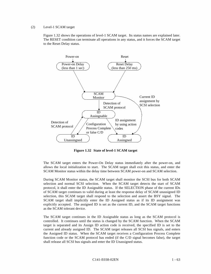
C141-E038-02EN 1 - 63
(2) Level-1 SCAM target
Figure 1.32 shows the operations of level-1 SCAM target. Its status names are explained later.The RESET condition can terminate all operations in any status, and it forces the SCAM targetto the Reset Delay status.
IDUnassingned
IDAssingned
IDAssingnable
ID assignmentby using actioncodes
Current IDassignment bySCSI selection
Detection ofSCAM protocol
ConfigurationProcess Completeor false C/D
Detection ofSCAM protocol
ResetPower-on
SCAMMonitor
Reset Delay(less than 250 ms)
Power-on Delay(less than 1 sec)
Figure 1.32 State of level-1 SCAM target
The SCAM target enters the Power-On Delay status immediately after the power-on, andallows the local initialization to start. The SCAM target shall exit this status, and enter theSCAM Monitor status within the delay time between SCAM power-on and SCAM selection.
During SCAM Monitor status, the SCAM target shall monitor the SCSI bus for both SCAMselection and normal SCSI selection. When the SCAM target detects the start of SCAMprotocol, it shall enter the ID Assignable status. If the SELECTION phase of the current IDsof SCAM target continues to valid during at least the response delay of SCAM unassigned IDselection, this SCAM target shall respond to the selection and assert the BSY signal. TheSCAM target shall implicitly enter the ID Assigned status as if its ID assignment wasexplicitly accepted. The assigned ID is set as the current ID, and the SCAM target functionsas the SCAM tolerant device.
The SCAM target continues in the ID Assignable status as long as the SCAM protocol iscontrolled. It continues until the status is changed by the SCAM function. When the SCAMtarget is separated and its Assign ID action code is received, the specified ID is set to thecurrent and already assigned ID. The SCAM target releases all SCSI bus signals, and entersthe Assigned ID status. When the SCAM target receives a Configuration Process Completefunction code or the SCAM protocol has ended (if the C/D signal becomes false), the targetshall release all SCSI bus signals and enter the ID Unassigned status.
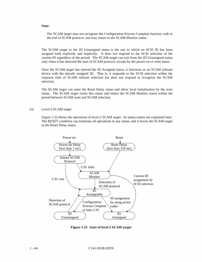
C141-E038-02EN1 - 64
Note:
The SCAM target may not recognize the Configuration Process Complete function code atthe end of SCAM protocol, and may return to the SCAM Monitor status.
The SCAM target in the ID Unassigned status is the one to which no SCSI ID has beenassigned both explicitly and implicitly. It does not respond to the SCSI selection of thecurrent ID regardless of the period. The SCAM target can exit from the ID Unassigned statusonly when it has detected the start of SCAM protocol, except for the power-on or reset status.
Once the SCAM target has entered the ID Assigned status, it functions as an SCAM tolerantdevice with the already assigned ID. That is, it responds to the SCSI selection within theresponse time of SCAM tolerant selection but does not respond or recognize the SCAMselection.
The SCAM target can enter the Reset Delay status and allow local initialization by the resetstatus. The SCAM target exists this status and enters the SCAM Monitor status within theperiod between SCAM reset and SCAM selection.
(3) Level-2 SCAM target
Figure 1.33 shows the operations of level-2 SCAM target. Its status names are explained later.The RESET condition can terminate all operations in any status, and it forces the SCAM targetto the Reset Delay status.
IDUnassingned
IDAssingned
IDAssingnable
ID assignmentby using actioncodes
Current IDassignment bySCSI selection
Detection ofSCAM protocol
ConfigurationProcess Completeor false C/D
Detection ofSCAM protocol
C/D: true
C/D: false
ResetPower-on
SCAMMonitor
Reset Delay(less than 250 ms)
Power-on Delay(less than 1 sec)
Initiate SCAMProtocol
Figure 1.33 State of level-2 SCAM target
C141-E038-02EN 1 - 65
The SCAM target enters the Power-On Delay status immediately after the power-on, and allows thelocal initialization to start. The SCAM target shall exit this status, and enter the Initial SCAMProtocol status within the delay time between SCAM power-on and SCAM selection.
During Initial SCAM Protocol status, the level-2 SCAM target arbitrates the SCSI bus without usingthe ID and performs the SCAM selection. After SCAM selection delay, the SCAM target checksthe SCSI bus and determines the C/D signal status. If the C/D signal is true, the SCAM initiatorexists and its SCAM target enters in the ID Assignable status. If the C/D signal is false, the SCAMinitiator does not exist and its SCAM target enters the SCAM Monitor status. Note that the level-2SCAM target starts the SCAM protocol only once after the power-on.
During SCAM Monitor status, the SCAM target shall monitor the SCSI bus for both SCAMselection and normal SCSI selection. When the SCAM target detects the start of SCAMprotocol, it shall enter the ID Assignable status. If the SELECTION phase of the current IDsof SCAM target continues to valid during at least the response delay of SCAM unassigned IDselection, this SCAM target shall respond to the selection and assert the BSY signal. TheSCAM target shall implicitly enter the ID Assigned status as if its ID assignment wasexplicitly accepted. The assigned ID is set as the current ID, and the SCAM target functionsas the SCAM tolerant device.
The SCAM target continues in the ID Assignable status as long as the SCAM protocol iscontrolled. It continues until the status is changed by the SCAM function. When the SCAMtarget is separated and its Assign ID action code is received, the specified ID is set to thecurrent and already assigned ID. The SCAM target releases all SCSI bus signals, and entersthe Assigned ID status. When the SCAM target receives a Configuration Process Completefunction code or the SCAM protocol has ended (if the C/D signal becomes false), the targetshall release all SCSI bus signals and enter the ID Unassigned status.
Note:
The SCAM target may not recognize the Configuration Process Complete function code atthe end of SCAM protocol, and may return to the SCAM Monitor status.
The SCAM target in the ID Unassigned status is the one to which no SCSI ID has beenassigned both explicitly and implicitly. It does not respond to the SCSI selection of thecurrent ID regardless of the period. The SCAM target can exit from the ID Unassigned statusonly when it has detected the start of SCAM protocol, except for the power-on or reset status.
Once the SCAM target has entered the ID Assigned status, it functions as an SCAM tolerant devicewith the already assigned ID. That is, it responds to the SCSI selection within the response time ofSCAM tolerant selection but does not respond or recognize the SCAM selection.
The SCAM target can enter the Reset Delay status and allow local initialization by the resetstatus. The SCAM target exists this status and enters the SCAM Monitor status within theperiod between SCAM reset and SCAM selection.
(4) Interconnection of various width buses
If an SCSI-3 device is mixed with an SCSI-1 or SCSI-2 device, a problem may occur. TheSCSI-3 TERMPWR requirements have been expanded to support the 16-bit data bus. During
C141-E038-02EN1 - 66
this time, the SCSI-1 and SCSI-2 devices cannot supply enough TERMPWR. Also, anadditional TERMPWR source (such as an SCSI-3 device) may be required.
When two buses having the different width are interconnected, the DATA BUS signal of thebus having a larger width shall be terminated with an adapter. The connector has beendesigned to electrically isolate the A and P shielded connectors from each other.
Two reserved lines (having A-cable contact numbers 23 and 24) and the open lines (having A-cable contact number 25) on the A cable are the TERMPWR lines (having the P-cable contactnumbers 33, 34 and 35) on the P cable.
An eight-bit device connected to the unbalanced P-cable shall keep open nine signals of DB(8to 15) and DB(P1).
An eight-bit device connected to the differential P-cable shall keep open 18 signals of +DB(15to 8), -DB(15 to 8), +DB(P1) and -DB(P1).
1.10 Ultra SCSI
1.10.1 Outline
The SCSI-3, Fast-20 Standard defines the characteristics of cables, signals, and transceiversrequired for 20 MB/s signal transmission. The services required to communicate with a higherlayer protocol is defined by the SCSI-3 Parallel Interface Standard.
In addition, the expansion to SCSI-3 parallel interface is defined to enhance the available datatransfer rate. Only the interface specifications associated with the higher data speed areincluded in this Standard.
1.10.2 Device connection
(1) Connection between an unbalanced transceiver and device
The maximum length of accumulated signal path between terminators shall be 3.0 m if up to four25-pF capacitance devices are used. The maximum length of accumulated signal path betweenterminators shall be 1.5 m if five to eight devices that have maximum capacitance are used. Whenconnecting nine or more devices, the specifications exceeding the minimum value defined in thismanual shall be controlled. The distance between devices should be equal to each other, and the lastdevice should locate close to the terminator as much as possible.
If the all bus elements (including cable, device interface, ambient noise, and other parameters)are controlled well to realize an environment better than the minimum required conditions, thepath may be extended and more devices may be connected (see Section 1.10.3 "UnbalancedI/O characteristics").
The signal path shall have the following impedance characteristics.
1) 90 +/-6 Ω for REQ and ACK signals2) 90 +/-10 Ω for all other signals
C141-E038-02EN 1 - 67
The stub length shall not exceed 0.1 m. It shall be measured from the transceiver positiontoward the connection point of trunk SCSI bus. The space between devices on the trunk SCSIbus shall be at least three times larger than the stub length to prevent clustered stubs.
The ground offset voltage between logical ground terminals on any two device connectorsshall be less than 50 mV.
1.10.3 Electrical characteristics of SCSI parallel interface
The Fast-20 parallel interface shall have one of the following electrical characteristics:
1) Either conductor of unbalanced driver and receiver, and each signal pair shall be active,and the other conductor shall be grounded.
2) Both conductors of differential driver and receiver, and each signal pair shall be active.
The unbalanced and differential transceivers cannot be used simultaneously.
(1) Unbalanced type options
a. Termination of unbalanced bus signals
All SCSI bus signals are common to all devices connected to the same bus. All signallines shall be terminated at their both ends by the terminators which are compatible to thetransceivers used for SCSI devices. The end of bus shall be defined at each end point.The end point can be inside of an SCSI device.
Unbalanced bus signals not defined as RESERVED, GROUND or TERMPWR shall be terminated ateach bus end securely. Each signal termination shall satisfy the following requirements:
1) Each terminator shall be powered from the TERMPWR line.
2) Each terminator shall feed the current to a signal line if the terminal voltage of this signalline is 2.5 VDC or less. This current shall not exceed 24 mA if the line voltage is greaterthan 0.2 VDC even when all other signal lines are driven with the 4.0 VDC power.
3) Each terminator shall not feed the current to a signal line if the terminal voltage of thissignal line exceeds 3.24 VDC.
4) All signal lines shall have the voltage of at least 2.5 VDC when released.
5) The terminator at each end of SCSI bus shall add a 25-pF capacitance maximum toeach signal (see Section 1.10.2).
6) No terminator shall be used if it connects the 220 Ω resistance to the 5V line and the330 Ω resistance to the ground.
Note:
These requirements shall be satisfied if any device supplies the TERMPWR.
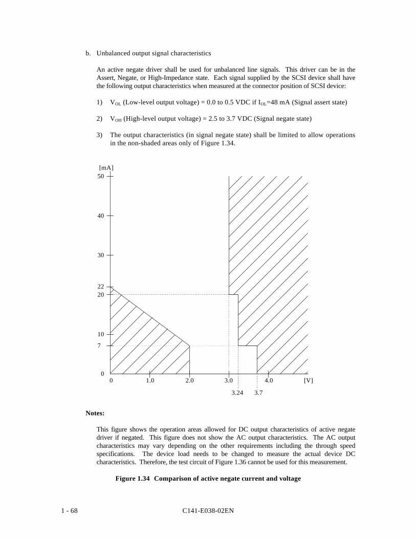
C141-E038-02EN1 - 68
b. Unbalanced output signal characteristics
An active negate driver shall be used for unbalanced line signals. This driver can be in theAssert, Negate, or High-Impedance state. Each signal supplied by the SCSI device shall havethe following output characteristics when measured at the connector position of SCSI device:
1) VOL (Low-level output voltage) = 0.0 to 0.5 VDC if IOL=48 mA (Signal assert state)
2) VOH (High-level output voltage) = 2.5 to 3.7 VDC (Signal negate state)
3) The output characteristics (in signal negate state) shall be limited to allow operationsin the non-shaded areas only of Figure 1.34.
10
7
3.73.24
[V]4.03.02.01.00
[mA]50
40
30
2220
0
Notes:
This figure shows the operation areas allowed for DC output characteristics of active negatedriver if negated. This figure does not show the AC output characteristics. The AC outputcharacteristics may vary depending on the other requirements including the through speedspecifications. The device load needs to be changed to measure the actual device DCcharacteristics. Therefore, the test circuit of Figure 1.36 cannot be used for this measurement.
Figure 1.34 Comparison of active negate current and voltage
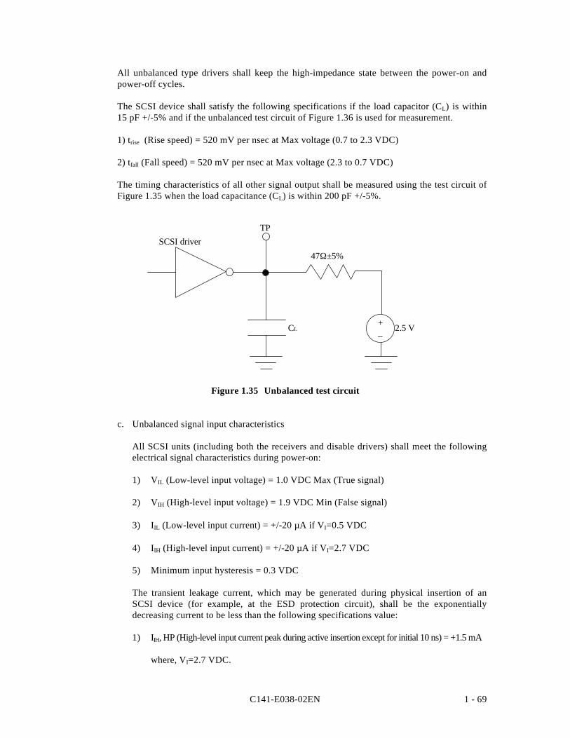
C141-E038-02EN 1 - 69
All unbalanced type drivers shall keep the high-impedance state between the power-on andpower-off cycles.
The SCSI device shall satisfy the following specifications if the load capacitor (CL) is within15 pF +/-5% and if the unbalanced test circuit of Figure 1.36 is used for measurement.
1) trise (Rise speed) = 520 mV per nsec at Max voltage (0.7 to 2.3 VDC)
2) tfall (Fall speed) = 520 mV per nsec at Max voltage (2.3 to 0.7 VDC)
The timing characteristics of all other signal output shall be measured using the test circuit ofFigure 1.35 when the load capacitance (CL) is within 200 pF +/-5%.
CL 2.5 V+–
47Ω±5%
TPSCSI driver
Figure 1.35 Unbalanced test circuit
c. Unbalanced signal input characteristics
All SCSI units (including both the receivers and disable drivers) shall meet the followingelectrical signal characteristics during power-on:
1) VIL (Low-level input voltage) = 1.0 VDC Max (True signal)
2) VIH (High-level input voltage) = 1.9 VDC Min (False signal)
3) IIL (Low-level input current) = +/-20 µA if VI=0.5 VDC
4) IIH (High-level input current) = +/-20 µA if VI=2.7 VDC
5) Minimum input hysteresis = 0.3 VDC
The transient leakage current, which may be generated during physical insertion of anSCSI device (for example, at the ESD protection circuit), shall be the exponentiallydecreasing current to be less than the following specifications value:
1) IIH, HP (High-level input current peak during active insertion except for initial 10 ns) = +1.5 mA
where, VI=2.7 VDC.
C141-E038-02EN1 - 70
2) THP (Transient current continuation time until it reaches 10% of peak) = 20 µs max.
If the transfer period is 100 ns or more, the REQ/REQQ and ACK/ACKQ glitch filterdefined by SPI shall be used.
During power-off, the SCSI devices shall satisfy the electrical characteristics of theabove IIL and IIH signals except for a physical insertion of SCSI device.
Note:
As the Fast-20 voltage threshold has a small tolerance, the power supply shall have themaximum allowance of 5% of the normal voltage.
d. Unbalanced signal I/O characteristics
The unbalanced signals shall have the following electrical characteristics when measuredat the connector position of an SCSI device:
• IL (Leakage current): –20 to +20 µA at 0.0 to 3.7 VDC (High-impedance state)
• Maximum signal characteristics: 25 µF when measured at the beginning of stub
Notes:
If an SCSI device has its board design based on the advanced semiconductortechnologies, its lumped capacitance can be reduce below 16 pF. If such device hasno switching terminator, its node capacitance can be further reduced. If the lumpedcapacitance of a node decreases, the SCSI bus impedance can evenly increase up to90 Ω. This can enhance the margin and can increase the number of connectiondevices. If the backplane design is used, the device margin can be increased and morenumber of devices can be connected to the bus.
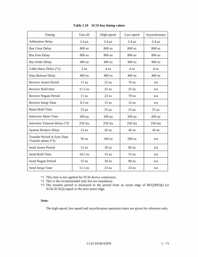
C141-E038-02EN 1 - 71
Table 1.10 SCSI bus timing values
Timing Fast-20 High-speed Low-speed Asynchronous
Arbitration Delay 2.4 µs 2.4 µs 2.4 µs 2.4 µs
Bus Clear Delay 800 ns 800 ns 800 ns 800 ns
Bus Free Delay 800 ns 800 ns 800 ns 800 ns
Bus Settle Delay 400 ns 400 ns 400 ns 400 ns
Cable Skew Delay (*1) 3 ns 4 ns 4 ns 4 ns
Data Release Delay 400 ns 400 ns 400 ns 400 ns
Receive Assert Period 11 ns 22 ns 70 ns n/a
Receive Hold time 11.5 ns 25 ns 25 ns n/a
Receive Negate Period 11 ns 22 ns 70 ns n/a
Receive Setup Time 6.5 ns 15 ns 15 ns n/a
Reset Hold Time 25 µs 25 µs 25 µs 25 µs
Selection Abort Time 200 µs 200 µs 200 µs 200 µs
Selection Timeout Delay (*2) 250 ms 250 ms 250 ms 250 ms
System Deskew Delay 15 ns 20 ns 45 ns 45 ns
Transfer Period in Sync DataTransfer phase (*3) 50 ns 100 ns 200 ns n/a
Send Assert Period 15 ns 30 ns 80 ns n/a
Send Hold Time 16.5 ns 33 ns 53 ns n/a
Send Negate Period 15 ns 30 ns 80 ns n/a
Send Setup Time 11.5 ns 23 ns 23 ns n/a
*1 This time is not applied for SCSI device connectors.*2 This is the recommended time but not mandatory.*3 The transfer period is measured in the period from an assert edge of REQ/REQQ (or
ACK/ACKQ) signal to the next assert edge.
Note:
The high-speed, low-speed and asynchronous operation times are given for reference only.

C141-E038-02EN 2 - 1
CHAPTER 2 SCSI MESSAGE
2.1 Message System
2.2 SCSI Pointer
2.3 Message Explanation
This chapter describes SCSI messages and their operations for controlling the operation sequence ofthe SCSI bus.
Note:
The IDD operates as a target device (TARG) on the SCSI bus. The IDD is referred to asthe TARG in this chapter except when its clear identification is required.
2.1 Message System
The message system provides procedures for information (or message) transfer between twoSCSI devices on the SCSI bus in order to control a series of bus phase sequence duringcommand execution. The messages are transferred over the SCSI data bus in the MESSAGEOUT and MESSAGE IN phases.
2.1.1 Message format
There are three message formats are listed below. The first byte of the message is a messagecode in any format. (See Figure 2.1.)
• One-byte message: This consists of a message code only.
• Two-byte message: Message code is between X’20’ and X'2F'. This consists of amessage code and one-byte length parameter.
• Extended message: This is a message of multiple bytes length message code ofX'01'.
The Extended message code and message length are specifiedin the message.
C141-E038-02EN2 - 2
Figure 2.1 Message format
2.1.2 Message type
Message types are shown in Tables 2.1 and 2.2. Function of each message is explained indetail in Section 2.3.
C141-E038-02EN 2 - 3
Table 2.1 SCSI message
Code(hex.)
Message Numberof bytes
Transferdirection
ANTrelease
00 COMMAND COMPLETE 1 TARG→INIT
01 EXTENDED MESSAGE(See Figure 2.1 and Table 2.2.)
n+2 TARG↔INIT (SeeTable 2.2)
02 SAVE DATA POINTER 1 TARG→INIT
04 DISCONNECT 1 TARG→INIT
05 INITIATOR DETECTED ERROR 1 TARG←INIT *
06 ABORT 1 TARG←INIT *
07 MESSAGE REJECT 1 TARG↔INIT *
08 NO OPERATION 1 TARG←INIT *
09 MESSAGE PARITY ERROR 1 TARG←INIT *
0A LINKED COMMAND COMPLETE 1 TARG→INIT
0B LINKED COMMAND COMPLETEWITH FLAG
1 TARG→INIT
0C BUS DEVICE RESET 1 TARG←INIT *
0D ABORT TAG 1 TARG←INIT *
0E CLEAR QUEUE 1 TARG←INIT *
11 TERMINATE I/O PROCESS 1 TARG←INIT *
20 SIMPLE QUEUE TAG 2 TARG↔INIT
21 HEAD OF QUEUE TAG 2 TARG←INIT
22 ORDERED QUEUE TAG 2 TARG←INIT
80
to
FF
IDENTIFY 1 TARG↔INIT
Note:
If a signal is identified by an asterisk (*) in the "ATN release" column, its ATN signalshall be made false at least 610 µs (Deskew Delay × 2) before the ACK signal of last byteof the message is made true by the INIT. The INIT should satisfy this requirement.However, the IDD does not force the INIT to satisfy this requirement but continues theMESSAGE OUT phase if the ATN signal is true.
C141-E038-02EN2 - 4
Table 2.2 Extended message
Code(hex.)
Message Numberof bytes
Transferdirection
ANTrelease
01 SYNCHRONOUS DATA TRANSFERREQUEST
5 TARG↔INIT *
03 WIDE DATA TRANSFER REQUEST 4 TARG↔INIT *
2.1.3 Message protocol
(1) Message implement requirements
All SCSI devices shall implement at least the COMMAND COMPLETE message. If a logicalunit number (LUN) for input and output operations is specified in the command (CDB), theminimum I/O operations required on the SCSI bus can be executed without using any messageother than the COMMAND COMPLETE message.
Also, the SCSI device should implement the MESSAGE REJECT message againstinappropriate message reception. The SCSI device must always implement the MESSAGEREJECT message if it supports any message other than the COMMAND COMPLETEmessage. In addition, the SCSI device supporting the parity check of SCSI data bus shouldimplement the MESSAGE PARITY ERROR message.
(2) ATTENTION condition
If SCSI device supports messages other than COMMAND COMPLETE message, the SCSIdevice creates ATTENTION condition or responds to the ATTENTION condition.
To indicate that the TARG can support messages other than COMMAND COMPLETEmessage, the TARG initiates MESSAGE OUT phase in response to ATTENTION condition.
Note:
If the INIT is in the ARBITRATION phase and if it generates an ATTENTION condition,it shall asserts the ATN signal before the SELECTION phase starts. If the INIT is not inthe ARBITRATION phase, it shall asserts the ATN signal when sending an SEL signal.
The TARG starts the MESSAGE OUT phase in response to the ATTENTION conditionimmediately after the end of SELECTION phase. It shows that the TARG supports messagesother than the COMMAND COMPLETE message.
If the TARG starts the INFORMATION TRANSFER phase (other than the MESSAGE OUTphase) when the INIT has generated an ATTENTION condition in the SELECTION phase, theINIT should negate the ATN before responding to the first ACK signal. If the ATTENTIONcondition is not generated during SELECTION phase, the TARG shall not send any messageexcept for the COMMAND COMPLETE message to the INIT.
C141-E038-02EN 2 - 5
(3) Path establishment of I/O operation
After the SELECTION phase, the IDENTIFY, ABORT, or BUS DEVICE RESET messagemust first be sent from the INIT to the TARG. The IDENTIFY message can be followed byanother message such as a SYNCHRONOUS DATA TRANSFER REQUEST message.
If tagged queuing technique is used, the QUEUE TAG message is issued immediately after theIDENTIFY message. This IDENTIFY message establishes an I/O operation path for thelogical unit specified by the INIT.
After the end of RESELECTION phase, the TARG shall first send the IDENTIFY message tothe INIT. This IDENTIFY message establishes an I/O operation path for the logical unitspecified by the TARG. If the tagged queuing is used, the SIMPLE QUEUE TAG message isissued after the IDENTIFY message.
If the INIT has enabled the disconnect processing and if it has established an I/O operationpath for the specific logical unit (by issuing the IDENTIFY message), the INIT shall set thecurrent pointer value to the same value (the initial value) of the Saved pointer value of thelogical unit. During reconnection processing (that is, when the IDENTIFY message is issuedafter the RESELECTION phase), the pointer is restored implicitly (and the Saved pointer valueis set to the current pointer value).
2.2 SCSI Pointer
The SCSI pointer feature is required by the INIT to control the command execution on theSCSI bus. It allows multiple TARGs and logical units to process multiple commandsconcurrently, and allows the TARG to retry processing in bus phases.
(1) Type of pointers
The following three types of SCSI pointers have been defined:
• Command pointer: controls and manages the command (CDB) transfer.
• Data pointer: controls and manages data transfer.
• Status pointer: controls and manages the status byte transfer.
All INITs must have these three types of pointers listed above. These pointers indicate INITmemory addresses for status byte storage, data transfer, and command (CDB) fetch whenviewed from the SCSI device functioning as a TARG.
The INIT needs to have one pair of current pointers and several pairs of saved pointers. Thecurrent pointers are used for the command which is being executed by the TARG currentlyassociated with the INIT. A current pointer value is updated every time one-byte informationis transferred in the INFORMATION TRANSFER phase. On the other hand, there is one pairof saved pointers for every command issued by the INIT (during its execution on the SCSI busor disconnection). The values of the current and saved pointers are identical (initial value)when the command is issued.
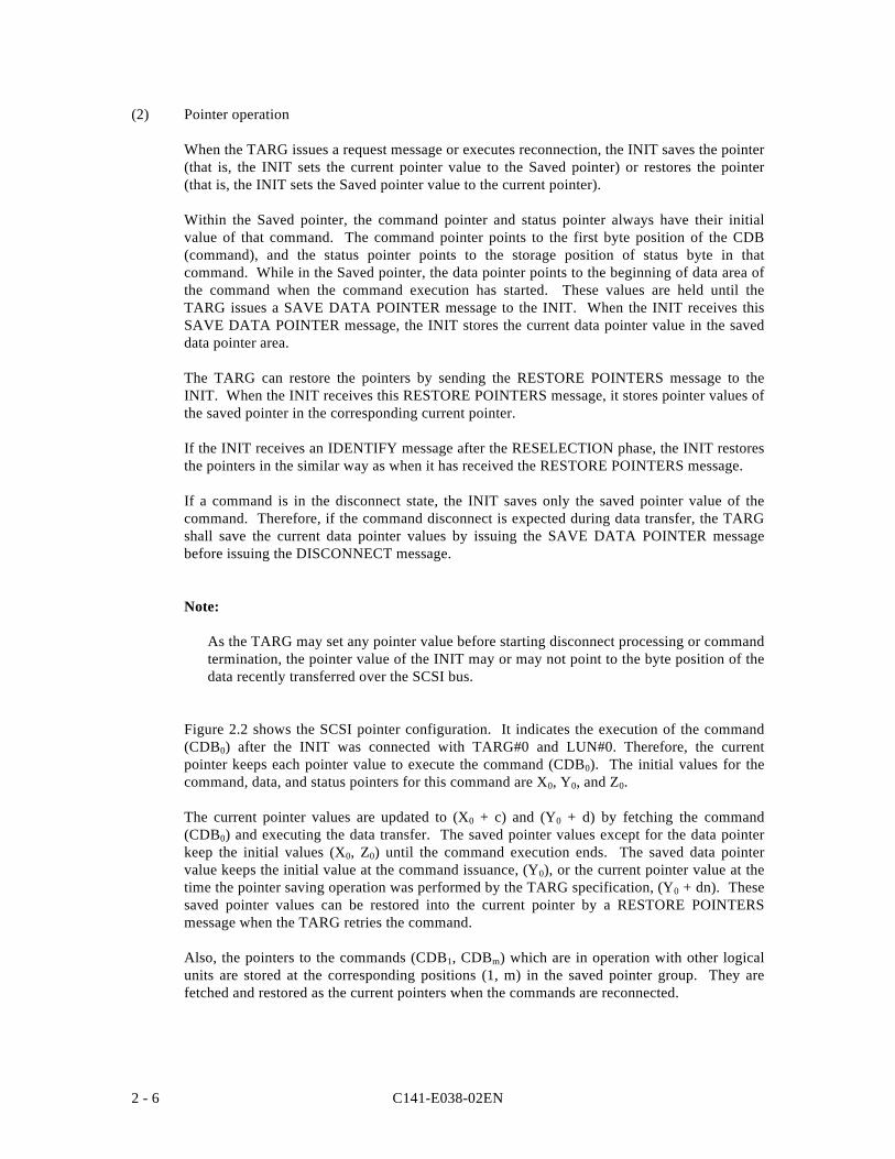
C141-E038-02EN2 - 6
(2) Pointer operation
When the TARG issues a request message or executes reconnection, the INIT saves the pointer(that is, the INIT sets the current pointer value to the Saved pointer) or restores the pointer(that is, the INIT sets the Saved pointer value to the current pointer).
Within the Saved pointer, the command pointer and status pointer always have their initialvalue of that command. The command pointer points to the first byte position of the CDB(command), and the status pointer points to the storage position of status byte in thatcommand. While in the Saved pointer, the data pointer points to the beginning of data area ofthe command when the command execution has started. These values are held until theTARG issues a SAVE DATA POINTER message to the INIT. When the INIT receives thisSAVE DATA POINTER message, the INIT stores the current data pointer value in the saveddata pointer area.
The TARG can restore the pointers by sending the RESTORE POINTERS message to theINIT. When the INIT receives this RESTORE POINTERS message, it stores pointer values ofthe saved pointer in the corresponding current pointer.
If the INIT receives an IDENTIFY message after the RESELECTION phase, the INIT restoresthe pointers in the similar way as when it has received the RESTORE POINTERS message.
If a command is in the disconnect state, the INIT saves only the saved pointer value of thecommand. Therefore, if the command disconnect is expected during data transfer, the TARGshall save the current data pointer values by issuing the SAVE DATA POINTER messagebefore issuing the DISCONNECT message.
Note:
As the TARG may set any pointer value before starting disconnect processing or commandtermination, the pointer value of the INIT may or may not point to the byte position of thedata recently transferred over the SCSI bus.
Figure 2.2 shows the SCSI pointer configuration. It indicates the execution of the command(CDB0) after the INIT was connected with TARG#0 and LUN#0. Therefore, the currentpointer keeps each pointer value to execute the command (CDB0). The initial values for thecommand, data, and status pointers for this command are X0, Y0, and Z0.
The current pointer values are updated to (X0 + c) and (Y0 + d) by fetching the command(CDB0) and executing the data transfer. The saved pointer values except for the data pointerkeep the initial values (X0, Z0) until the command execution ends. The saved data pointervalue keeps the initial value at the command issuance, (Y0), or the current pointer value at thetime the pointer saving operation was performed by the TARG specification, (Y0 + dn). Thesesaved pointer values can be restored into the current pointer by a RESTORE POINTERSmessage when the TARG retries the command.
Also, the pointers to the commands (CDB1, CDBm) which are in operation with other logicalunits are stored at the corresponding positions (1, m) in the saved pointer group. They arefetched and restored as the current pointers when the commands are reconnected.
C141-E038-02EN 2 - 7
Figure 2.2 SCSI pointer configuration
C141-E038-02EN2 - 8
2.3 Message Explanation
This section explains the function of each message. The following symbols are used formessage identification.
Symbols:
(I→T): The message which can be sent from the INIT to the TARG only.(T→I): The message which can be sent from the TARG to the INIT only.(I↔T): The message which can be sent between the INIT and TARG in any direction.
2.3.1 COMMAND COMPLETE message: X'00'(T→→I)
The COMMAND COMPLETE message indicates that an unlinked command or a series oflinked commands have been executed and that a valid status information has been posted tothe INIT.
This message notifies the INIT the validity of status information but the command may or maynot have been executed normally. The command completion status is indicated by the statusbyte which is sent in the STATUS phase prior to this message.
When the TARG sends the status byte to the INIT, the TARG always sends this message afterthe STATUS phase even if the normal command (CDB) transfer has failed (due to a parityerror of SCSI data bus in MESSAGE OUT or COMMAND phase).
When the TARG completes normal message transfer, it enters the BUS FREE phase. TheTARG determines that the message transfer has completed normally if the ATN signal is falsewhen the ACK signal becomes false.
2.3.2 SAVE DATA POINTER message: X'02'(T→→I)
The SAVE DATA POINTER message requests the INIT to save the current data pointer.When receiving this message, the INIT stores the value of current data pointer into the Savedpointer for the currently connected LUN. For the disconnection message, see Section 2.3.3.
2.3.3 DISCONNECT message: X'04' (T→→I)
The DISCONNECT message informs to the INIT that the TARG disconnects the SCSI bustemporary. After the TARG has sent this message, it enters the BUS FREE phase and thedisconnection completes. The TARG determines that the message transfer has completednormally if the ATN message is false when the ACK signal becomes false.
The TARG continues command processing by itself, and reconnects the INIT when necessary(by reconnect processing) to continue command execution on the SCSI bus.
This message cannot request the INIT for saving of the current data pointer.
C141-E038-02EN 2 - 9
Note:
To start disconnect processing during data transfer, the TARG must send the SAVE DATAPOINTER message for saving of data pointer before sending this message. This isrequired even if all bytes of data specified by the command have already been transferred.
2.3.4 INITIATOR DETECTED ERROR message: X'05'(I→→T)
The INITIATOR DETECTED ERROR message informs to the TARG that the INIT hasdetected an error which allows command retry by the TARG. The error cause may beassociated with the SCSI bus operations or INIT internal operations.
If this message is posted, the current pointer value is unreliable. Section 3.1 explains thedetails of recovery processing when the IDD receives this message.
2.3.5 ABORT message: X'06' (I→→T)
The ABORT message requests the TARG to clear the currently executing or queued I/Ooperations. When the TARG receives this message, it immediately performs the following(regardless of the ATN signal status).
If the LUN has been determined prior to this message, the TARG clears all of the currentlyexecuting or queued I/O operations which have been initiated by the source INIT of thismessage, and enters the BUS FREE phase. All of the hold data and status information, or thesense data of the logical unit and INIT are cleared. If the I/O operations are cleared by thismessage, their status byte and end messages are not sent to the INIT. This message does notaffect on the I/O operations initiated by another INIT.
If the LUN has not been determined prior to this message, the TARG enters the BUS FREEphase without any operation. This message does not affect on the currently executing orqueued I/O operations.
If this message is issued to the LUN which does not have the information about the currentlyexecuting or queued I/O operations or sense data status, the TARG does not generate an errorcondition but enters the BUS FREE phase.
To clear the disconnected I/O operations, the INIT can send the IDENTIFY and the ABORTmessages in succession immediately after the TARG selection (in SELECTION phase).
Note:
The BUS DEVICE RESET, CLEAR QUEUE, ABORT, and ABORT TAG messages canclear one or more I/O operations before they terminates normally.
• BUS DEVICE RESET message: Clears all I/O operations of all INITs existing on allLUNs of the TARG.
• CLEAR QUEUE message: Clears all I/O operations of all INITs existing on a specificLUN.
C141-E038-02EN2 - 10
• ABORT message: Clears all I/O operations of a specific INIT existing on a specificLUN.
• ABORT TAG message: Clears a single I/O operation only.
2.3.6 MESSAGE REJECT message: X'07'(I↔↔T)
The MESSAGE REJECT message indicates that the recently received message or messagebytes are inappropriate or has not been implemented.
When the INIT sends this message, to allow the TARG to identify the rejected message, itshall assert the ATN signal before negating the ACK signal associated when the TARGreceived a message to be rejected in the MESSAGE IN phase. If the TARG receives thismessage anytime except when it responds to the ATN signal, it shall reject this message.
When the TARG sends this message, the TARG shall enter the MESSAGE IN phase and sendthis message after negating the ACK signal associated with the rejected message if it isreceived in the MESSAGE OUT phase. This is required to allow the INIT to identify therejected message.
Section 3.1 explains the IDD operation details when the INIT returns this message in responseto the message sent by the IDD.
2.3.7 NO OPERATION message: X'08' (I→→T)
The NO OPERATION message does not result in any operation. If the INIT has no validmessages which can be sent in response to a send request from the TARG (in MESSAGE OUTphase), the INIT sends this message to the TARG.
2.3.8 MESSAGE PARITY ERROR message: X'09' (I→→T)
The MESSAGE PARITY ERROR message notifies the TARG that a parity error has beendetected in the message byte recently received by the INIT.
To allow the TARG to identify the message having the parity error, the INIT shall assert theATN signal, generate an ATTENTION condition, and send this message first. Then, the INITshall negate the ACK signal associated with the message which indicates a parity error in theMESSAGE IN phase.
Section 3.1 explains the IDD operation details when the INIT returns this message in responseto the message sent by the IDD.
2.3.9 LINKED COMMAND COMPLETE message: X'0A'(T→→I)
The LINKED COMMAND COMPLETE message indicates that the link command (with flagbit 0) has been executed normally and that the valid status byte has been posted to the INIT.When the INIT receives this message, it shall update both the current pointer and Savedpointer to the initial values of the next linked command.
C141-E038-02EN 2 - 11
2.3.10 LINKED COMMAND COMPLETE WITH FLAG message: X'0B'(T→→I)
The LINKED COMMAND COMPLETE WITH FLAG message indicates that the linkcommand (with flag bit 1) has been executed normally and that the valid status byte has beenposted to the INIT. When the INIT receives this message, it shall update both the currentpointer and Saved pointer to the initial values of the next linked command.
For example, the INIT can generate an interrupt to software after executing the commandwhose flag bit has been set to logical 1 within a series of linked commands.
2.3.11 BUS DEVICE RESET message: X'0C' (I→→T)
The BUS DEVICE RESET message requests the TARG to clear all of the currently executingor queued I/O operations (or commands). The TARG shall clear both the I/O operationsinitiated by the INIT of this message source and I/O operations of all INITs. When the TARGreceives this message, it shall enter the BUS FREE phase immediately (regardless of thesubsequent ATN signal status).
2.3.12 ABORT TAG message: X'0D' (I→→T)
The ABORT TAG message is valid only when the tagged queuing is supported. When theTARG receives this message normally, it enters the BUS FREE phase. The TARG clears thecurrent I/O operation and stops its current execution. The medium contents may have beenmodified before the execution is aborted. In either case, the hold status or data of the I/Ooperation is cleared. No status or end message is sent to the INIT. This message does notaffect on the held status, data, and commands of the I/O operations which are being executedor queued by another unit. Also, this message does not abort another I/O operation which isqueued in the INIT of this message source.
The system environment and conditions previously established by the MODE SELECTparameter are not changed by this message.
2.3.13 CLEAR QUEUE message: X'0E'(I→→T)
When the TARG receives the CLEAR QUEUE message, it enters the BUS FREE phase. TheTARG operates in the similar way as when it receives a series of ABORT messages from eachINIT. This message clears all I/O operations currently being executed or queued in thespecified logical unit. The medium contents may have been modified before the execution isaborted. All status and data held in all INITs are cleared. No status or message is sent to theINIT. If the I/O operations of INITs, which differ from the INIT of this message source, arecleared, a UNIT ATTENTION condition is generated for those INITs. When the UNITATTENTION condition is reported, the Sense data indicates the COMMANDS CLEAREDBY ANOTHER INITIATOR [=2F-00].
The system environment and conditions previously established by the MODE SELECTparameter are not changed by this message.
C141-E038-02EN2 - 12
2.3.14 TERMINATE I/O PROCESS message: X'11' (I→→T)
The TERMINATE I/O PROCESS message notifies the TARG that the currently executing I/Ooperations are terminated. When the TARG receives this message, it shall terminate the currentI/O operations and returns a COMMAND TERMINATE status. At this time, the sense dataindicating the "NO SENSE [=0] / I/O PROCESS TERMINATED [=00-06]" sense key or sensecode is generated. This message does not affect on the I/O operations currently queued orexecuted by another INIT or logical unit. However, if a command is terminated by thismessage, the subsequent queued commands may be affected by the Queue Error Recoveryoption which is defined in the Control Mode page of MODE SELECT parameter.
If the terminated I/O operation includes the data transfer (in DATA IN or DATA OUT phase),the Valid bit of sense data is set to logical 1 and the information field shows the following:
• If the transfer byte length or parameter list length is specified in the command descriptionblock (CDB), a difference between the transfer length of this CDB and the normallytransferred byte length is set in the information field.
• If the number of transfer blocks is specified in the command description block (CDB), adifference between the specified block count and the normally transferred block count isset in the information field.
If the terminated I/O operation does not include the data transfer, the TARG sets the Valid bitof sense data to logical 0 and terminates the I/O operation with the COMMANDTERMINATE status. The sense key or sense code of the sense data indicates the "NO SENSE[=0] / I/O PROCESS TERMINATED [=00-06]."
If the TARG detects another I/O operation error, it ignores this message, generates an errorstatus and sense data appropriate to that error, and terminates the I/O operations.
After the TARG has completed all command processing (including data reading, writing andother processing) the TARG may receive the TERMINATE I/O PROCESS message beforeterminating the I/O operations, the TARG ignores the TERMINATE I/O PROCESS messageand terminates the I/O operations in the usual way.
If the TARG receives the TERMINATE I/O PROCESS message before the CDB is transferred(that is, before completion of COMMAND phase), or if this message is issued to the TARGwhich does not have the currently executing or queued I/O operations, the TARG sets theValid bit of sense data to logical 0 and terminates the I/O operations with the COMMANDTERMINATE status. At this time, the sense key or sense code of the sense data indicates the"NO SENSE [=0] / I/O PROCESS TERMINATED [=00-06]."
If the specified I/O operations are placed in the command queue and not executed yet, theTARG immediately terminates these I/O operations with the COMMAND TERMINATEDstatus regardless of the queuing operation status. At this time, the sense key or sense code ofthe sense data indicates the "NO SENSE [=0] / I/O PROCESS TERMINATED [=00-06]", andthe Valid bit is set to logical 0.
If the TARG cannot terminate the current I/O operations, it responds to the INIT by returning aMESSAGE REJECT message and continues the I/O operations in the usual way.
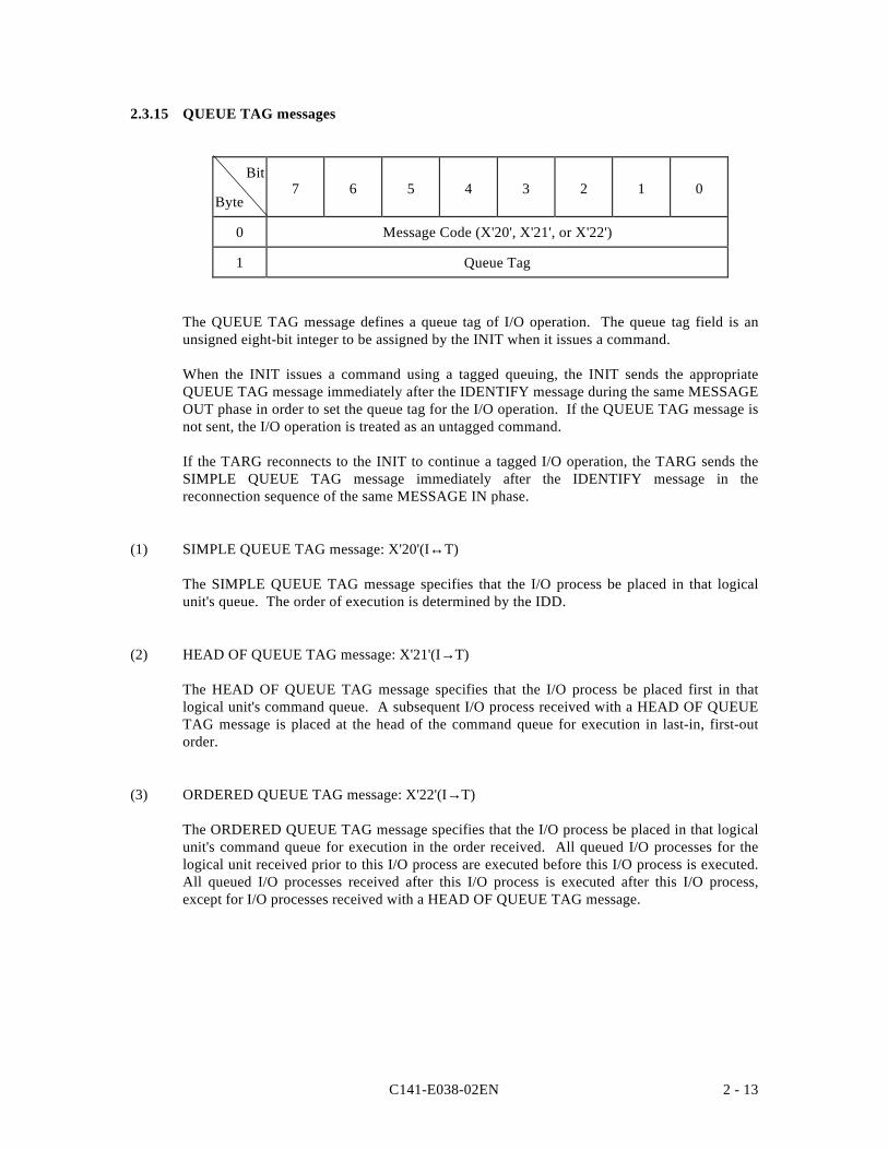
C141-E038-02EN 2 - 13
2.3.15 QUEUE TAG messages
Bit
Byte7 6 5 4 3 2 1 0
0 Message Code (X'20', X'21', or X'22')
1 Queue Tag
The QUEUE TAG message defines a queue tag of I/O operation. The queue tag field is anunsigned eight-bit integer to be assigned by the INIT when it issues a command.
When the INIT issues a command using a tagged queuing, the INIT sends the appropriateQUEUE TAG message immediately after the IDENTIFY message during the same MESSAGEOUT phase in order to set the queue tag for the I/O operation. If the QUEUE TAG message isnot sent, the I/O operation is treated as an untagged command.
If the TARG reconnects to the INIT to continue a tagged I/O operation, the TARG sends theSIMPLE QUEUE TAG message immediately after the IDENTIFY message in thereconnection sequence of the same MESSAGE IN phase.
(1) SIMPLE QUEUE TAG message: X'20'(I↔T)
The SIMPLE QUEUE TAG message specifies that the I/O process be placed in that logicalunit's queue. The order of execution is determined by the IDD.
(2) HEAD OF QUEUE TAG message: X'21'(I→T)
The HEAD OF QUEUE TAG message specifies that the I/O process be placed first in thatlogical unit's command queue. A subsequent I/O process received with a HEAD OF QUEUETAG message is placed at the head of the command queue for execution in last-in, first-outorder.
(3) ORDERED QUEUE TAG message: X'22'(I→T)
The ORDERED QUEUE TAG message specifies that the I/O process be placed in that logicalunit's command queue for execution in the order received. All queued I/O processes for thelogical unit received prior to this I/O process are executed before this I/O process is executed.All queued I/O processes received after this I/O process is executed after this I/O process,except for I/O processes received with a HEAD OF QUEUE TAG message.
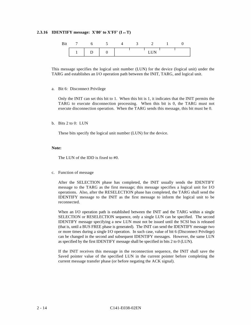
C141-E038-02EN2 - 14
2.3.16 IDENTIFY message: X'80' to X'FF' (I↔↔T)
Bit 7 6 5 4 3 2 1 0
1 D 0 LUN
This message specifies the logical unit number (LUN) for the device (logical unit) under theTARG and establishes an I/O operation path between the INIT, TARG, and logical unit.
a. Bit 6: Disconnect Privilege
Only the INIT can set this bit to 1. When this bit is 1, it indicates that the INIT permits theTARG to execute disconnection processing. When this bit is 0, the TARG must notexecute disconnection operation. When the TARG sends this message, this bit must be 0.
b. Bits 2 to 0: LUN
These bits specify the logical unit number (LUN) for the device.
Note:
The LUN of the IDD is fixed to #0.
c. Function of message
After the SELECTION phase has completed, the INIT usually sends the IDENTIFYmessage to the TARG as the first message; this message specifies a logical unit for I/Ooperations. Also, after the RESELECTION phase has completed, the TARG shall send theIDENTIFY message to the INIT as the first message to inform the logical unit to bereconnected.
When an I/O operation path is established between the INIT and the TARG within a singleSELECTION or RESELECTION sequence, only a single LUN can be specified. The secondIDENTIFY message specifying a new LUN must not be issued until the SCSI bus is released(that is, until a BUS FREE phase is generated). The INIT can send the IDENTIFY message twoor more times during a single I/O operation. In such case, value of bit 6 (Disconnect Privilege)can be changed in the second and subsequent IDENTIFY messages. However, the same LUNas specified by the first IDENTIFY message shall be specified in bits 2 to 0 (LUN).
If the INIT receives this message in the reconnection sequence, the INIT shall save theSaved pointer value of the specified LUN in the current pointer before completing thecurrent message transfer phase (or before negating the ACK signal).
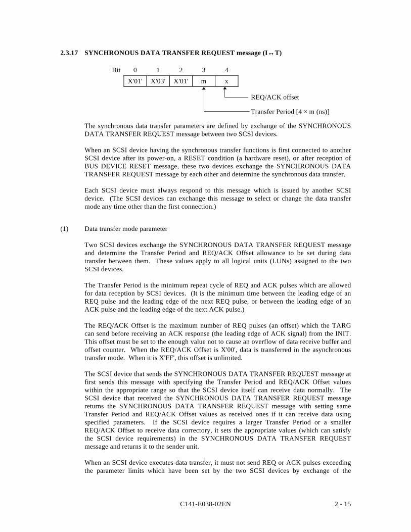
C141-E038-02EN 2 - 15
2.3.17 SYNCHRONOUS DATA TRANSFER REQUEST message (I↔↔T)
Bit 0 1 2 3 4
X'01' X'03' X'01' m x
REQ/ACK offset
Transfer Period [4 × m (ns)]
The synchronous data transfer parameters are defined by exchange of the SYNCHRONOUSDATA TRANSFER REQUEST message between two SCSI devices.
When an SCSI device having the synchronous transfer functions is first connected to anotherSCSI device after its power-on, a RESET condition (a hardware reset), or after reception ofBUS DEVICE RESET message, these two devices exchange the SYNCHRONOUS DATATRANSFER REQUEST message by each other and determine the synchronous data transfer.
Each SCSI device must always respond to this message which is issued by another SCSIdevice. (The SCSI devices can exchange this message to select or change the data transfermode any time other than the first connection.)
(1) Data transfer mode parameter
Two SCSI devices exchange the SYNCHRONOUS DATA TRANSFER REQUEST messageand determine the Transfer Period and REQ/ACK Offset allowance to be set during datatransfer between them. These values apply to all logical units (LUNs) assigned to the twoSCSI devices.
The Transfer Period is the minimum repeat cycle of REQ and ACK pulses which are allowedfor data reception by SCSI devices. (It is the minimum time between the leading edge of anREQ pulse and the leading edge of the next REQ pulse, or between the leading edge of anACK pulse and the leading edge of the next ACK pulse.)
The REQ/ACK Offset is the maximum number of REQ pulses (an offset) which the TARGcan send before receiving an ACK response (the leading edge of ACK signal) from the INIT.This offset must be set to the enough value not to cause an overflow of data receive buffer andoffset counter. When the REQ/ACK Offset is X'00', data is transferred in the asynchronoustransfer mode. When it is X'FF', this offset is unlimited.
The SCSI device that sends the SYNCHRONOUS DATA TRANSFER REQUEST message atfirst sends this message with specifying the Transfer Period and REQ/ACK Offset valueswithin the appropriate range so that the SCSI device itself can receive data normally. TheSCSI device that received the SYNCHRONOUS DATA TRANSFER REQUEST messagereturns the SYNCHRONOUS DATA TRANSFER REQUEST message with setting sameTransfer Period and REQ/ACK Offset values as received ones if it can receive data usingspecified parameters. If the SCSI device requires a larger Transfer Period or a smallerREQ/ACK Offset to receive data correctory, it sets the appropriate values (which can satisfythe SCSI device requirements) in the SYNCHRONOUS DATA TRANSFER REQUESTmessage and returns it to the sender unit.
When an SCSI device executes data transfer, it must not send REQ or ACK pulses exceedingthe parameter limits which have been set by the two SCSI devices by exchange of the
C141-E038-02EN2 - 16
SYNCHRONOUS DATA TRANSFER REQUEST message. However, the SCSI device cantransfer data using a larger Transfer Period or a smaller REQ/ACK Offset.
After normal exchange of the SYNCHRONOUS DATA TRANSFER REQUEST message, thetwo SCSI devices shall set the data transfer mode depending on the response (the returnedmessage) by the SCSI device which has first received this message. Table 2.3 defines the datatransfer mode to be selected.
Table 2.3 Definition of data transfer mode by message exchange
Responded message Data transfer mode
SYNCHRONOUS DATATRANSFER REQUESTREQ/ACK Offset ≥ 1
Synchronous mode:Each SCSI device executes data transfer usingthe Transfer Period value equal to or greaterthan the specified value and REQ/ACK Offsetvalue equal to or smaller than the specifiedvalue specified in the SYNCHRONOUS DATATRANSFER REQUEST message from theopposite SCSI device.
SYNCHRONOUS DATATRANSFER REQUESTREQ/ACK Offset =0
Asynchronous mode
MESSAGE REJECT Asynchronous mode
(2) Procedures of the message exchange initiated by the INIT
If the INIT has recognized the synchronous data transfer to be set, it asserts the ATN signalthat is, generating an ATTENTION condition for message exchange, and requests the TARGto receive the SYNCHRONOUS DATA TRANSFER REQUEST message.
After the MESSAGE OUT phase has completed normally, the TARG shall return theSYNCHRONOUS DATA TRANSFER REQUEST message or the MESSAGE REJECTmessage to the INIT. If the ACK signal is still true after the TARG has received theSYNCHRONOUS DATA TRANSFER REQUEST message, the TARG can cancel theMESSAGE OUT phase and can enter the MESSAGE IN phase to return the message. If theTARG cannot return the message, the two SCSI devices shall select the asynchronous datatransfer mode between them.
Even if the TARG returns the SYNCHRONOUS DATA TRANSFER REQUEST messagewith specifying 1 and more to the REQ/ACK Offset value, when the INIT first sends theMESSAGE PARITY ERROR, MESSAGE REJECT, or INITIATOR DETECTED ERRORmessage to the TARG by asserting the ATN signal in the MESSAGE IN phase, the modesetting for synchronous-mode transfer for both the INIT and TARG is regarded to have failed,and data transfer between the two SCSI devices must be set to the asynchronous mode.
C141-E038-02EN 2 - 17
(3) Procedures of the message exchange initiated by the TARG
If the TARG has recognized the synchronous data transfer to be set and if the synchronousdata transfer request is enabled by the CHANGE DEFINITION command, the TARG sendsthe SYNCHRONOUS DATA TRANSFER REQUEST message to the INIT. The INIT shallreturn the SYNCHRONOUS DATA TRANSFER REQUEST or MESSAGE REJECT messageby asserting the ATN signal before negating the ACK signal of the last byte ofSYNCHRONOUS DATA TRANSFER REQUEST message sent from the TARG. If the INITcannot respond to this message, the two SCSI devices shall select the asynchronous datatransfer mode between them.
The INIT and the TARG shall continue the synchronous data transfer even if the INIT hasresponded with the SYNCHRONOUS DATA TRANSFER REQUEST message. Thissynchronous transfer mode shall be continued until the MESSAGE OUT phase is terminatednormally by transition of TARG to the INFORMATION TRANSFER phase (it indicates thatno parity error has been detected). If the TARG fails to receive the response by the INITnormally after the specified number of retries, the TARG shall negate the BSY signal and shallenter the BUS FREE phase immediately without executing another INFORMATIONTRANSFER phase. The INIT shall consider it as the unsuccessful message exchange and thetwo SCSI devices shall select the asynchronous data transfer mode between them.
If the TARG enters the MESSAGE IN phase immediately after the INIT has responded withthe SYNCHRONOUS DATA TRANSFER REQUEST message, and if the TARG first sendsthe MESSAGE REJECT message to the INIT, the INIT shall consider it as the unsuccessfulselection of synchronous data transfer. The two SCSI devices shall select the asynchronousdata transfer mode between them.
If the ATN signal is still true when the message is returned by the INIT in MESSAGE OUTphase, if the TARG has normally received multiple messages in succession, and if the TARGreceives the ABORT message after the SYNCHRONOUS DATA TRANSFER REQUESTmessage, the TARG shall complete to process the SYNCHRONOUS DATA TRANSFERREQUEST message and validate the transfer mode selection. Then, the TARG shall executethe ABORT message. If the TARG receives the ABORT message before receiving theSYNCHRONOUS DATA TRANSFER REQUEST message, the two SCSI devices shall selectthe asynchronous data transfer mode between them.
(4) Valid cycle for the data transfer mode
After the exchange of SYNCHRONOUS DATA TRANSFER REQUEST message, theselected data transfer mode and the synchronous data transfer parameters shall be kept valid onthese SCSI devices until when:
• A BUS DEVICE RESET message is received.• A RESET condition (a hardware reset) occurs.• The data transfer mode or parameter is changed between the two SCSI devices.• Power off• Reception of the WIDE DATA TRANSFER REQUEST message
The default data transfer mode between SCSI devices is asynchronous data transfer. Theasynchronous data transfer mode shall be selected when the power supply is turned on, a BUSDEVICE RESET message is received, a RESET condition occurs, or a WIDE DATATRANSFER REQUEST message is received.
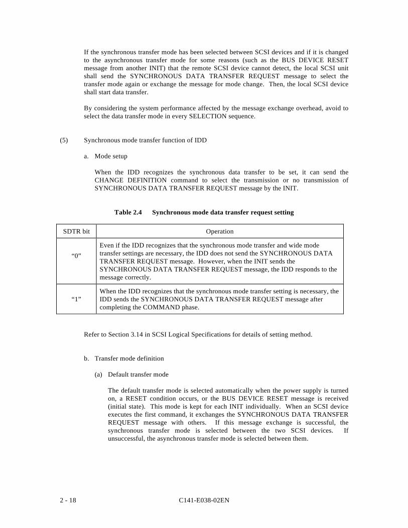
C141-E038-02EN2 - 18
If the synchronous transfer mode has been selected between SCSI devices and if it is changedto the asynchronous transfer mode for some reasons (such as the BUS DEVICE RESETmessage from another INIT) that the remote SCSI device cannot detect, the local SCSI unitshall send the SYNCHRONOUS DATA TRANSFER REQUEST message to select thetransfer mode again or exchange the message for mode change. Then, the local SCSI deviceshall start data transfer.
By considering the system performance affected by the message exchange overhead, avoid toselect the data transfer mode in every SELECTION sequence.
(5) Synchronous mode transfer function of IDD
a. Mode setup
When the IDD recognizes the synchronous data transfer to be set, it can send theCHANGE DEFINITION command to select the transmission or no transmission ofSYNCHRONOUS DATA TRANSFER REQUEST message by the INIT.
Table 2.4 Synchronous mode data transfer request setting
SDTR bit Operation
“0”
Even if the IDD recognizes that the synchronous mode transfer and wide modetransfer settings are necessary, the IDD does not send the SYNCHRONOUS DATATRANSFER REQUEST message. However, when the INIT sends theSYNCHRONOUS DATA TRANSFER REQUEST message, the IDD responds to themessage correctly.
“1”When the IDD recognizes that the synchronous mode transfer setting is necessary, theIDD sends the SYNCHRONOUS DATA TRANSFER REQUEST message aftercompleting the COMMAND phase.
Refer to Section 3.14 in SCSI Logical Specifications for details of setting method.
b. Transfer mode definition
(a) Default transfer mode
The default transfer mode is selected automatically when the power supply is turnedon, a RESET condition occurs, or the BUS DEVICE RESET message is received(initial state). This mode is kept for each INIT individually. When an SCSI deviceexecutes the first command, it exchanges the SYNCHRONOUS DATA TRANSFERREQUEST message with others. If this message exchange is successful, thesynchronous transfer mode is selected between the two SCSI devices. Ifunsuccessful, the asynchronous transfer mode is selected between them.
C141-E038-02EN 2 - 19
(b) Transfer mode establishment
The default transfer mode is released, and the synchronous transfer mode or theasynchronous transfer mode is selected by the exchange of SYNCHRONOUS DATATRANSFER REQUEST message.
This mode is kept for each INIT individually and data transfer mode and synchronousmode parameters of each INIT differ each other. Data is transferred in the transfermode selected between the INIT based on the SCSI ID of the INIT which is identifiedin the SELECTION phase.
If the INIT is in this state, the IDD does not send the SYNCHRONOUS DATATRANSFER REQUEST message to request for reselection of the transfer mode orchanging the synchronous transfer mode parameters. However, if the INIT returns theSYNCHRONOUS DATA TRANSFER REQUEST message again, the IDD respondsto it as described later and it selects the data transfer mode again or sets thesynchronous data transfer parameters again.
If the retry fails in the MESSAGE IN or MESSAGE OUT phase when theSYNCHRONOUS DATA TRANSFER REQUEST message is exchanged, or if thetransfer mode selection sequence has failed, the transfer mode between the INITmoves to the default transfer mode.
(c) Transfer mode when the SCSI ID is not defined for INITs
Even if the SCSI ID of the INIT is not posted in the SELECTION phase (if a singleINIT is used and if it does not use the RESELECTION phase), the message can beexchanged and the data transfer mode can be selected between the IDD and the INIT.In this case, the IDD sets a unique data transfer mode for the INIT which has theundefined SCSI ID. If the system dynamically uses two types of SELECTION phase(where the SCSI ID of the INIT is posted and it is not posted), the transfer mode mustbe selected for each data transmission.
c. Transfer mode setup from INIT to IDD
Table 2.5 shows the IDD response to the first SYNCHRONOUS DATA TRANSFERREQUEST message sent from the INIT. Also, this table lists the data transfer modes setbetween the INIT and IDD by the response.
The INIT can send the SYNCHRONOUS DATA TRANSFER REQUEST messageanytime. However, the IDD shall send this message to the INIT for selection ofsynchronous data transfer mode if the INIT has failed to send the SYNCHRONOUSDATA TRANSFER REQUEST message by the end of COMMAND phase. It is requiredwhen the IDD still maintains the default transfer mode to the INIT and when thesynchronous transfer request is enabled by the CHANGE DEFINITION command (seeParagraph "d").
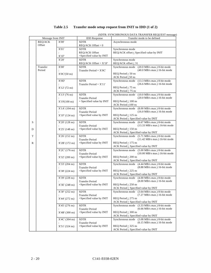
C141-E038-02EN2 - 20
Table 2.5 Transfer mode setup request from INIT to IDD (1 of 2)
(SDTR: SYNCHRONOUS DATA TRANSFER REQUEST message)Message from INIT IDD Response Transfer mode to be defined
REQ/ACKOffset
X'00' SDTRREQ/ACK Offset = 0
Asynchronous mode
X'01':X'1F'
SDTRREQ/ACK Offset=Specified value by INIT
Synchronous modeREQ/ACK offset < Specified value by INIT
X'20':
SDTRREQ/ACK Offset = X'1F'
Synchronous modeREQ/ACK offset < 31
TransferPeriod
X'00':X'0C'(50 ns)
SDTRTransfer Period = X'0C'
Synchronous mode (20.0 MB/s max.) 8-bit mode(40.0 MB/s max.) 16-bit mode
REQ Period > 50 nsACK Period >50 ns
X'0D':X'12' (72 ns)
SDTRTransfer Period = X'11'
Synchronous mode (13.3 MB/s max.) 8-bit mode(26.6 MB/s max.) 16-bit mode
REQ Period > 75 nsACK Period > 75 ns
X'13' (76 ns):X'19'(100 ns)
SDTRTransfer Period= Specified value by INIT
Synchronous mode (10.0 MB/s max.) 8-bit mode(20.0 MB/s max.) 16-bit mode
REQ Period > 100 nsACK Period >100 ns
X'1A' (104 ns):X'1F' (124 ns)
SDTRTransfer Period=Specified value by INIT
Synchronous mode (8.00 MB/s max.) 8-bit mode(16.0 MB/s max.) 16-bit mode
REQ Period > 125 nsACK Period > Specified value by INIT
S
D
X'20' (128 ns):X'25' (148 ns)
SDTRTransfer Period=Specified value by INIT
Synchronous mode (6.67 MB/s max.) 8-bit mode(13.33 MB/s max.) 16-bit mode
REQ Period > 150 nsACK Period > Specified value by INIT
T
R
X'26' (152 ns):X'2B' (172 ns)
SDTRTransfer Period=Specified value by INIT
Synchronous mode (5.71 MB/s max.) 8-bit mode(11.42 MB/s max.) 16-bit mode
REQ Period > 175 nsACK Period > Specified value by INIT
X'2C' (176 ns):X'32' (200 ns)
SDTRTransfer Period=Specified value by INIT
Synchronous mode (5.00 MB/s max.) 8-bit mode(10.00 MB/s max.) 16-bit mode
REQ Period > 200 nsACK Period > Specified value by INIT
X'33' (204 ns):X'38' (224 ns)
SDTRTransfer Period=Specified value by INIT
Synchronous mode (4.44 MB/s max.) 8-bit mode(8.88 MB/s max.) 16-bit mode
REQ Period > 225 nsACK Period > Specified value by INIT
X'39' (228 ns):X'3E' (248 ns)
SDTRTransfer Period=Specified value by INIT
Synchronous mode (4.00 MB/s max.) 8-bit mode(8.00 MB/s max.) 16-bit mode
REQ Period > 250 nsACK Period > Specified value by INIT
X'3F' (252 ns):X'44' (272 ns)
SDTRTransfer Period=Specified value by INIT
Synchronous mode (3.64 MB/s max.) 8-bit mode(7.27 MB/s max.) 16-bit mode
REQ Period > 275 nsACK Period > Specified value by INIT
X'45' (276 ns):X'4B' (300 ns)
SDTRTransfer Period=Specified value by INIT
Synchronous mode (3.33 MB/s max.) 8-bit mode(6.66 MB/s max.) 16-bit mode
REQ Period > 300 nsACK Period > Specified value by INIT
X'4C' (304 ns):X'51' (324 ns)
SDTRTransfer Period=Specified value by INIT
Synchronous mode (3.08 MB/s max.) 8-bit mode(6.15 MB/s max.) 16-bit mode
REQ Period > 325 nsACK Period > Specified value by INIT
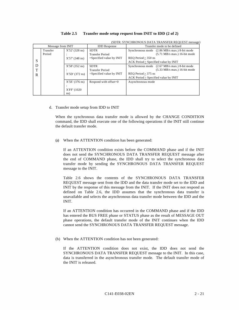
C141-E038-02EN 2 - 21
Table 2.5 Transfer mode setup request from INIT to IDD (2 of 2)
(SDTR: SYNCHRONOUS DATA TRANSFER REQUEST message)Message from INIT IDD Response Transfer mode to be defined
TransferPeriod
X'52' (328 ns):X'57' (348 ns)
SDTRTransfer Period=Specified value by INIT
Synchronous mode (2.86 MB/s max.) 8-bit mode(5.71 MB/s max.) 16-bit mode
REQ Period > 350 nsACK Period > Specified value by INIT
X'58' (352 ns):X'5D' (372 ns)
SDTRTransfer Period=Specified value by INIT
Synchronous mode (2.67 MB/s max.) 8-bit mode(5.33 MB/s max.) 16-bit mode
REQ Period > 375 nsACK Period > Specified value by INIT
X'5E' (376 ns):X'FF' (1020ns)
Respond with offset=0 Asynchronous mode
d. Transfer mode setup from IDD to INIT
When the synchronous data transfer mode is allowed by the CHANGE CONDITIONcommand, the IDD shall execute one of the following operations if the INIT still continuethe default transfer mode.
(a) When the ATTENTION condition has been generated:
If an ATTENTION condition exists before the COMMAND phase and if the INITdoes not send the SYNCHRONOUS DATA TRANSFER REQUEST message afterthe end of COMMAND phase, the IDD shall try to select the synchronous datatransfer mode by sending the SYNCHRONOUS DATA TRANSFER REQUESTmessage to the INIT.
Table 2.6 shows the contents of the SYNCHRONOUS DATA TRANSFERREQUEST message sent from the IDD and the data transfer mode set to the IDD andINIT by the response of this message from the INIT. If the INIT does not respond asdefined on Table 2.6, the IDD assumes that the synchronous data transfer isunavailable and selects the asynchronous data transfer mode between the IDD and theINIT.
If an ATTENTION condition has occurred in the COMMAND phase and if the IDDhas entered the BUS FREE phase or STATUS phase as the result of MESSAGE OUTphase operations, the default transfer mode of the INIT continues when the IDDcannot send the SYNCHRONOUS DATA TRANSFER REQUEST message.
(b) When the ATTENTION condition has not been generated:
If the ATTENTION condition does not exist, the IDD does not send theSYNCHRONOUS DATA TRANSFER REQUEST message to the INIT. In this case,data is transferred in the asynchronous transfer mode. The default transfer mode ofthe INIT is released.
SDTR
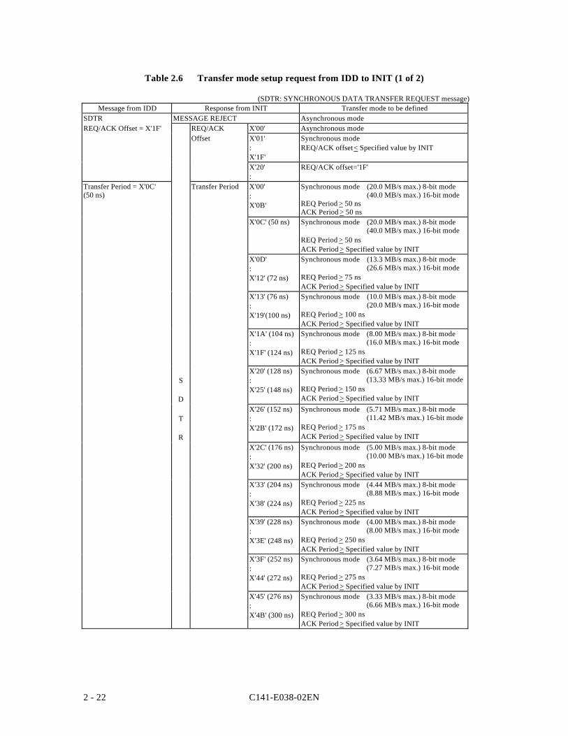
C141-E038-02EN2 - 22
Table 2.6 Transfer mode setup request from IDD to INIT (1 of 2)
(SDTR: SYNCHRONOUS DATA TRANSFER REQUEST message)Message from IDD Response from INIT Transfer mode to be defined
SDTR MESSAGE REJECT Asynchronous modeREQ/ACK Offset = X'1F' REQ/ACK X'00' Asynchronous mode
Offset X'01':X'1F'
Synchronous modeREQ/ACK offset < Specified value by INIT
X'20':
REQ/ACK offset='1F'
Transfer Period = X'0C'(50 ns)
Transfer Period X'00':X'0B'
Synchronous mode (20.0 MB/s max.) 8-bit mode(40.0 MB/s max.) 16-bit mode
REQ Period > 50 nsACK Period > 50 ns
X'0C' (50 ns) Synchronous mode (20.0 MB/s max.) 8-bit mode(40.0 MB/s max.) 16-bit mode
REQ Period > 50 nsACK Period > Specified value by INIT
X'0D':X'12' (72 ns)
Synchronous mode (13.3 MB/s max.) 8-bit mode(26.6 MB/s max.) 16-bit mode
REQ Period > 75 nsACK Period > Specified value by INIT
X'13' (76 ns):X'19'(100 ns)
Synchronous mode (10.0 MB/s max.) 8-bit mode(20.0 MB/s max.) 16-bit mode
REQ Period > 100 nsACK Period > Specified value by INIT
X'1A' (104 ns):X'1F' (124 ns)
Synchronous mode (8.00 MB/s max.) 8-bit mode(16.0 MB/s max.) 16-bit mode
REQ Period > 125 nsACK Period > Specified value by INIT
S
D
X'20' (128 ns):X'25' (148 ns)
Synchronous mode (6.67 MB/s max.) 8-bit mode(13.33 MB/s max.) 16-bit mode
REQ Period > 150 nsACK Period > Specified value by INIT
T
R
X'26' (152 ns):X'2B' (172 ns)
Synchronous mode (5.71 MB/s max.) 8-bit mode(11.42 MB/s max.) 16-bit mode
REQ Period > 175 nsACK Period > Specified value by INIT
X'2C' (176 ns):X'32' (200 ns)
Synchronous mode (5.00 MB/s max.) 8-bit mode(10.00 MB/s max.) 16-bit mode
REQ Period > 200 nsACK Period > Specified value by INIT
X'33' (204 ns):X'38' (224 ns)
Synchronous mode (4.44 MB/s max.) 8-bit mode(8.88 MB/s max.) 16-bit mode
REQ Period > 225 nsACK Period > Specified value by INIT
X'39' (228 ns):X'3E' (248 ns)
Synchronous mode (4.00 MB/s max.) 8-bit mode(8.00 MB/s max.) 16-bit mode
REQ Period > 250 nsACK Period > Specified value by INIT
X'3F' (252 ns):X'44' (272 ns)
Synchronous mode (3.64 MB/s max.) 8-bit mode(7.27 MB/s max.) 16-bit mode
REQ Period > 275 nsACK Period > Specified value by INIT
X'45' (276 ns):X'4B' (300 ns)
Synchronous mode (3.33 MB/s max.) 8-bit mode(6.66 MB/s max.) 16-bit mode
REQ Period > 300 nsACK Period > Specified value by INIT
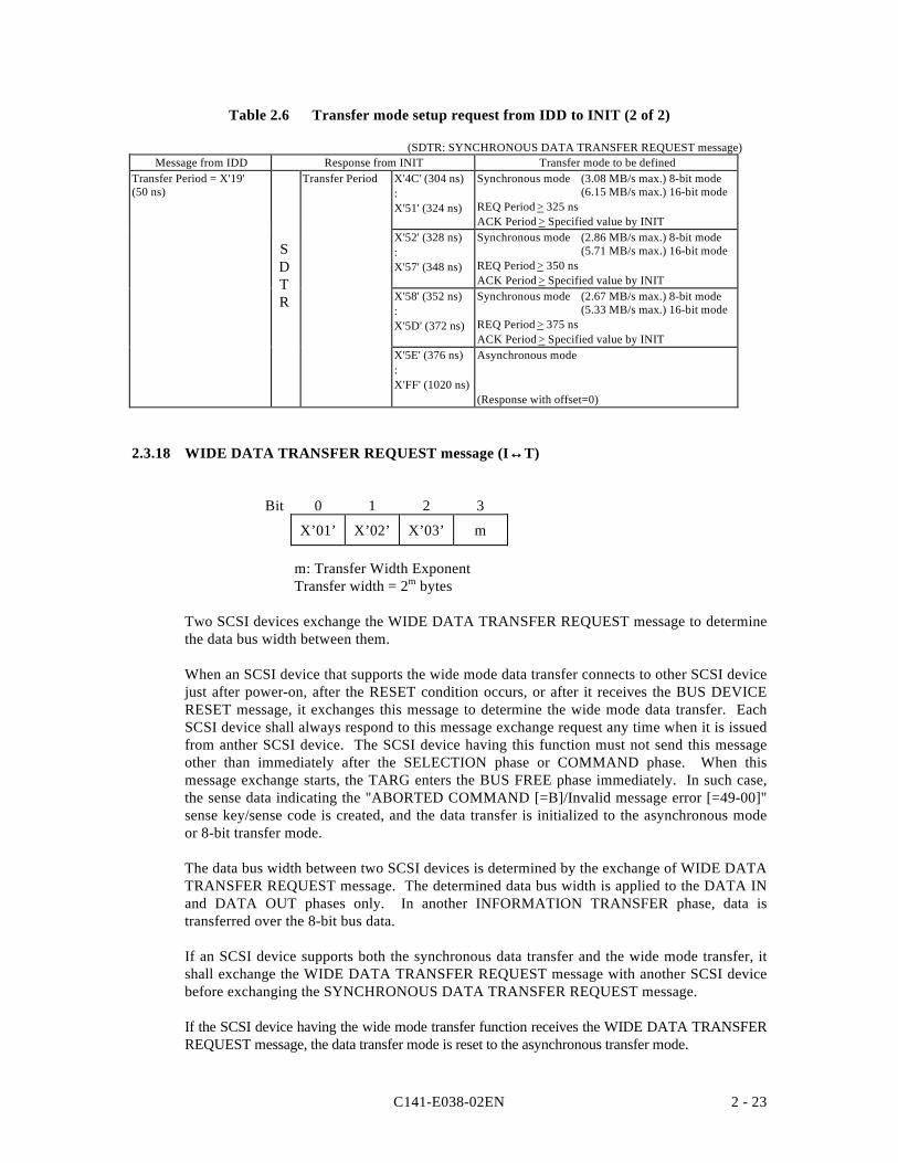
C141-E038-02EN 2 - 23
Table 2.6 Transfer mode setup request from IDD to INIT (2 of 2)
(SDTR: SYNCHRONOUS DATA TRANSFER REQUEST message)Message from IDD Response from INIT Transfer mode to be defined
Transfer Period = X'19'(50 ns)
Transfer Period X'4C' (304 ns):X'51' (324 ns)
Synchronous mode (3.08 MB/s max.) 8-bit mode(6.15 MB/s max.) 16-bit mode
REQ Period > 325 nsACK Period > Specified value by INIT
X'52' (328 ns):X'57' (348 ns)
Synchronous mode (2.86 MB/s max.) 8-bit mode(5.71 MB/s max.) 16-bit mode
REQ Period > 350 nsACK Period > Specified value by INIT
X'58' (352 ns):X'5D' (372 ns)
Synchronous mode (2.67 MB/s max.) 8-bit mode(5.33 MB/s max.) 16-bit mode
REQ Period > 375 nsACK Period > Specified value by INIT
X'5E' (376 ns):X'FF' (1020 ns)
Asynchronous mode
(Response with offset=0)
2.3.18 WIDE DATA TRANSFER REQUEST message (I↔↔T)
Bit 0 1 2 3
X’01’ X’02’ X’03’ m
m: Transfer Width ExponentTransfer width = 2m bytes
Two SCSI devices exchange the WIDE DATA TRANSFER REQUEST message to determinethe data bus width between them.
When an SCSI device that supports the wide mode data transfer connects to other SCSI devicejust after power-on, after the RESET condition occurs, or after it receives the BUS DEVICERESET message, it exchanges this message to determine the wide mode data transfer. EachSCSI device shall always respond to this message exchange request any time when it is issuedfrom anther SCSI device. The SCSI device having this function must not send this messageother than immediately after the SELECTION phase or COMMAND phase. When thismessage exchange starts, the TARG enters the BUS FREE phase immediately. In such case,the sense data indicating the "ABORTED COMMAND [=B]/Invalid message error [=49-00]"sense key/sense code is created, and the data transfer is initialized to the asynchronous modeor 8-bit transfer mode.
The data bus width between two SCSI devices is determined by the exchange of WIDE DATATRANSFER REQUEST message. The determined data bus width is applied to the DATA INand DATA OUT phases only. In another INFORMATION TRANSFER phase, data istransferred over the 8-bit bus data.
If an SCSI device supports both the synchronous data transfer and the wide mode transfer, itshall exchange the WIDE DATA TRANSFER REQUEST message with another SCSI devicebefore exchanging the SYNCHRONOUS DATA TRANSFER REQUEST message.
If the SCSI device having the wide mode transfer function receives the WIDE DATA TRANSFERREQUEST message, the data transfer mode is reset to the asynchronous transfer mode.
SDTR
C141-E038-02EN2 - 24
(1) Wide mode parameters
The data bus width between two SCSI devices is determined by exchanging the WIDE DATATRANSFER REQUEST message. This value applies to all logical units assigned to these twoSCSI devices.
The valid data bus width is determined by the Transfer Width Exponent value.
An SCSI device, which sends this message first, specifies the maximum possible data buswidth and sends the WIDE DATA TRANSFER REQUEST message. The destination SCSIdevice returns the same value if it can support the requested data bus width. If impossible, thedestination SCSI device answers the possible data bus width.
After the WIDE DATA TRANSFER REQUEST messages have been exchanged normally, thetwo SCSI devices shall set the data bus width based on the response (the return message) bythe SCSI device which has first received the message. Table 2.7 defines the data bus width tobe set by message exchange.
Table 2.7 Data bus width defined by message exchange
Response message Data bus width
WIDE DATA TRANSFER REQUESTTransfer Width Exponent > 1
Data is transferred using the responded data buswidth.
WIDE DATA TRANSFER REQUESTTransfer Width Exponent = 0
8-bit data transfer
MESSAGE REJECT message 8-bit data transfer
(2) Message exchange started by the INIT
If the INIT needs to select the wide data transfer mode, it asserts the ATN signal to startmessage exchange. Then, the INIT requests the TARG to receive the WIDE DATATRANSFER REQUEST message. When the MESSAGE OUT phase has terminated normally,the TARG shall return an appropriate WIDE DATA TRANSFER REQUEST message to theINIT. If the TARG cannot return the message normally, these two SCSI devices shall set the8-bit data bus width between them.
If the INIT asserts the ATN signal in the MESSAGE IN phase and sends the MESSAGEPARTY ERROR message or the MESSAGE REJECT message even if the TARG returns aWIDE DATA TRANSFER REQUEST message which indicates a non-zero value in itsTransfer Width Exponent field, the two SCSI devices shall set the 8-bit data bus widthbetween them.
C141-E038-02EN 2 - 25
(3) Message exchange started by the TARG
If the TARG recognizes the need of message exchange and if the wide data mode transferrequest is enabled by the CHANGE DEFINITION command, the TARG sends the WIDEDATA TRANSFER REQUEST message to the INIT. The INIT shall assert the ATN signaland return the WIDE DATA TRANSFER REQUEST message or the MESSAGE REJECTmessage before negating the ACK signal of the last byte of WIDE DATA TRANSFERREQUEST message which has been sent from the TARG. If the INIT cannot respond to thismessage, the two SCSI devices shall set the 8-bit data bus width between them.
Both the INIT and the TARG shall not consider the completion of WIDE DATA TRANSFERREQUEST message exchange until the TARG terminates the MESSAGE OUT phase byentering another INFORMATION TRANSFER phase (which indicates that no parity error hasbeen detected) even if the INIT responds with the WIDE DATA TRANSFER REQUESTmessage. If the TARG cannot normally receive a response message by the INIT after thespecified number of retries, the TARG shall immediately negate the BSY signal and enter theBUS FREE phase without starting another INFORMATION TRANSFER phase.
The INIT shall consider it as the unsuccessful message exchange, and the two SCSI devicesshall set the 8-bit data bus width between them.
If the TARG enters the MESSAGE IN phase and first sends the MESSAGE REJECT messageto the INIT immediately after the INIT has responded with the WIDE DATA TRANSFERREQUEST message, such message exchange is made invalid and the two SCSI devices shallset the 8-bit data bus width between them.
(4) Valid period of wide data transfer mode
After the exchange of WIDE DATA TRANSFER REQUEST message, the data bus widthdetermined between the two SCSI devices shall be kept valid until when:
• BUS DEVICE RESET MESSAGE reception• RESET condition ("hardware RESET") occurrence• Transfer width change between the same SCSI devices• Power turned off
The default data bus width is 8 bits between SCSI devices. The data bus width shall beinitialized to 8 bits when the power supply is turned on, a BUS DEVICE RESET message isreceived, or when a RESET condition occurs.
(5) Wide mode transfer of IDD
a. Mode setting
When the IDD recognizes the wide mode data transfer to be set, the INIT can selectwhether the IDD sends the WIDE DATA TRANSFER REQUEST message to the INIT bysending the CHANGE DEFINITION command.
For details on setting, refer to Section 3.1.4 in the SCSI Logical Specifications.
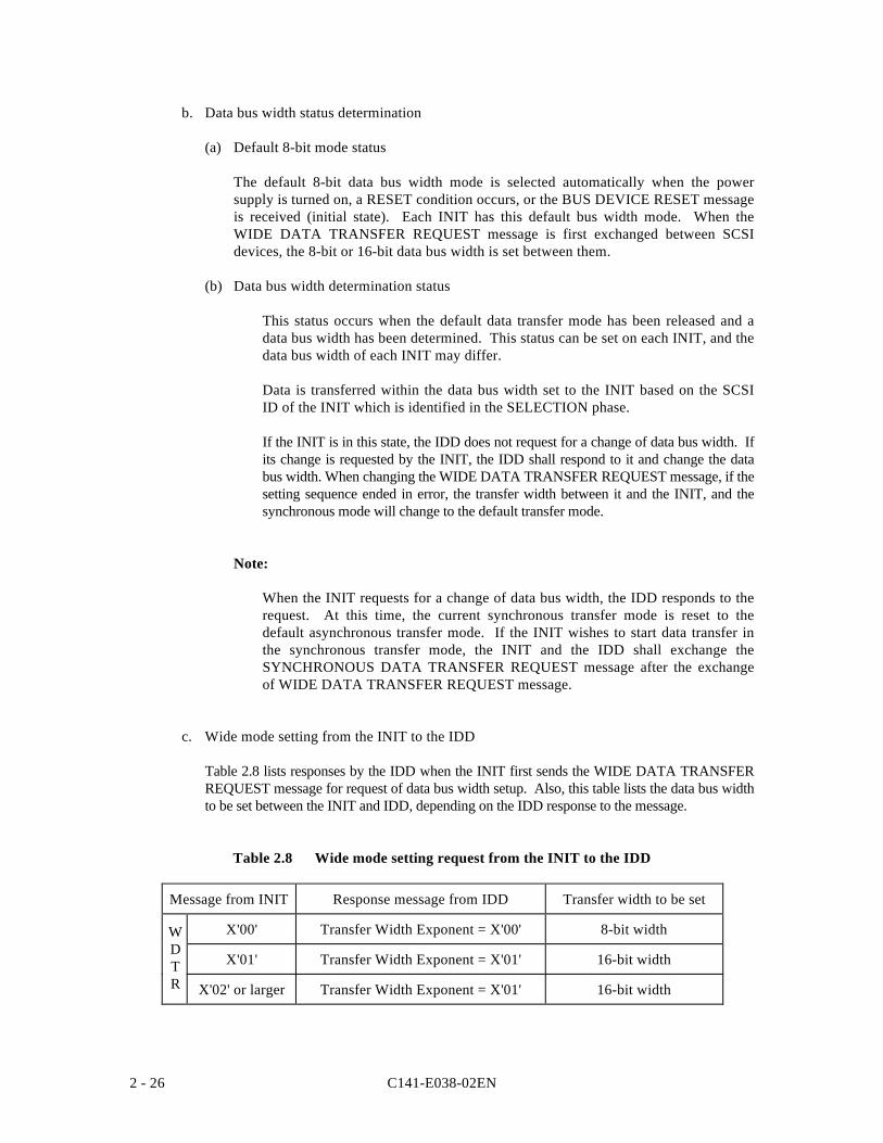
C141-E038-02EN2 - 26
b. Data bus width status determination
(a) Default 8-bit mode status
The default 8-bit data bus width mode is selected automatically when the powersupply is turned on, a RESET condition occurs, or the BUS DEVICE RESET messageis received (initial state). Each INIT has this default bus width mode. When theWIDE DATA TRANSFER REQUEST message is first exchanged between SCSIdevices, the 8-bit or 16-bit data bus width is set between them.
(b) Data bus width determination status
This status occurs when the default data transfer mode has been released and adata bus width has been determined. This status can be set on each INIT, and thedata bus width of each INIT may differ.
Data is transferred within the data bus width set to the INIT based on the SCSIID of the INIT which is identified in the SELECTION phase.
If the INIT is in this state, the IDD does not request for a change of data bus width. Ifits change is requested by the INIT, the IDD shall respond to it and change the databus width. When changing the WIDE DATA TRANSFER REQUEST message, if thesetting sequence ended in error, the transfer width between it and the INIT, and thesynchronous mode will change to the default transfer mode.
Note:
When the INIT requests for a change of data bus width, the IDD responds to therequest. At this time, the current synchronous transfer mode is reset to thedefault asynchronous transfer mode. If the INIT wishes to start data transfer inthe synchronous transfer mode, the INIT and the IDD shall exchange theSYNCHRONOUS DATA TRANSFER REQUEST message after the exchangeof WIDE DATA TRANSFER REQUEST message.
c. Wide mode setting from the INIT to the IDD
Table 2.8 lists responses by the IDD when the INIT first sends the WIDE DATA TRANSFERREQUEST message for request of data bus width setup. Also, this table lists the data bus widthto be set between the INIT and IDD, depending on the IDD response to the message.
Table 2.8 Wide mode setting request from the INIT to the IDD
Message from INIT Response message from IDD Transfer width to be set
X'00' Transfer Width Exponent = X'00' 8-bit width
X'01' Transfer Width Exponent = X'01' 16-bit width
X'02' or larger Transfer Width Exponent = X'01' 16-bit width
WDTR
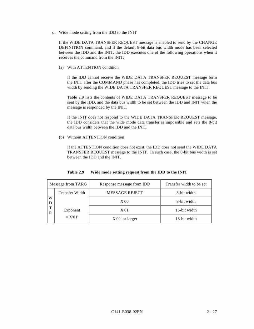
C141-E038-02EN 2 - 27
d. Wide mode setting from the IDD to the INIT
If the WIDE DATA TRANSFER REQUEST message is enabled to send by the CHANGEDEFINITION command, and if the default 8-bit data bus width mode has been selectedbetween the IDD and the INIT, the IDD executes one of the following operations when itreceives the command from the INIT:
(a) With ATTENTION condition
If the IDD cannot receive the WIDE DATA TRANSFER REQUEST message formthe INIT after the COMMAND phase has completed, the IDD tries to set the data buswidth by sending the WIDE DATA TRANSFER REQUEST message to the INIT.
Table 2.9 lists the contents of WIDE DATA TRANSFER REQUEST message to besent by the IDD, and the data bus width to be set between the IDD and INIT when themessage is responded by the INIT.
If the INIT does not respond to the WIDE DATA TRANSFER REQUEST message,the IDD considers that the wide mode data transfer is impossible and sets the 8-bitdata bus width between the IDD and the INIT.
(b) Without ATTENTION condition
If the ATTENTION condition does not exist, the IDD does not send the WIDE DATATRANSFER REQUEST message to the INIT. In such case, the 8-bit bus width is setbetween the IDD and the INIT.
Table 2.9 Wide mode setting request from the IDD to the INIT
Message from TARG Response message from IDD Transfer width to be set
Transfer Width MESSAGE REJECT 8-bit width
X'00' 8-bit width
Exponent X'01' 16-bit width
= X'01' X'02' or larger 16-bit width
WDTR

C141-E038-02EN 3 - 1
CHAPTER 3 ERROR RECOVERY
3.1 Error Conditions and Retry Procedure
3.2 Recovery Control
This chapter describes the SCSI bus errors and their recovery by the IDD.
Note:
If a severe error has occurred, the IDD may switch the SCSI bus to the BUS FREE phasewithout sending the DISCONNECT or COMMAND COMPLETE message to the INIT.In such case, the IDD clears all information of the currently executing commands and doesnot report the command completion (or reconnection) to the INIT.
If the SCSI bus is switched to the BUS FREE phase in a sequence other than the normalbus sequence, the INIT shall consider that the currently executing command hasterminated abnormally. In such case, the IDD may or may not generate a sense data of thiserror. However, the INIT should issue the REQUEST SENSE message to obtain the errorinformation.
3.1 Error Conditions and Retry Procedure
(1) MESSAGE OUT phase parity error
When the IDD detects a parity error of the SCSI bus during the MESSAGE OUT phase, itdoes not make retry and proceeds to the next procedure. For details, see Section 1.6.9.
If the LUN is already identified, the IDD terminates the currently executing command with theCHECK CONDITION status. At this time, the sense key/sense code of the sense dataindicates the "ABORTED COMMAND [=B]/SCSI parity error [=47-nn]." If this happensafter the status is reported, the IDD enters the BUSS FREE phase and the same sense data isretained. The IDD ignores the ATTENTION condition until it enters the BUS FREE phase. Ifthe LUN is not identified by the IDENTIFY message or the LUN field of CDB, the IDD doesnot generate the sense data and enters the BUS FREE phase immediately.
C141-E038-02EN3 - 2
(2) COMMAND phase parity error
When the IDD detects a parity error in the COMMAND phase, it does not make retry andproceeds to the next procedure.
If the LUN is already identified by the IDENTIFY message, the IDD terminates the commandwith the CHECK CONDITION status. The sense key/sense code of the sense data indicatesthe "ABORTED COMMAND [=B]/SCSI parity error [=47-99]."
If the LUN is not identified, the IDD does not generate the sense data and enters the BUSFREE phase immediately.
(3) DATA OUT phase parity error
When the IDD detects a parity error of SCSI bus in the DATA OUT phase, it does not makeretry and proceeds to the next procedure.
The IDD terminates the currently executing command with the CHECK CONDITION status.The sense key/sense code of the sense data indicates the "ABORTED COMMAND [=B]/SCSIparity error [=47-A1]."
(4) Receiving a INITIATOR DETECTED ERROR message
When the IDD receives an INITIATOR DETECTED ERROR message from the INIT, the IDDdoes not make retry and proceeds to the next procedure.
If the LUN is already identified, the IDD terminates the currently executing command with theCHECK CONDITION status. The sense key/sense code of the sense data indicates the"ABORTED COMMAND [=B]/INITIATOR DETECTED ERROR message received [=48-00]." If the LUN is not identified yet, the IDD does not generate the sense data and enters theBUS FREE phase immediately. If the STATUS phase has already completed, the IDD alsoenters the BUS FREE phase but does not send the status again.
(5) Receiving a MESSAGE PARITY ERROR message
If the IDD receives a MESSAGE PARITY ERROR message from the INIT as its response tothe ATTENTION condition (MESSAGE OUT phase) generated at the MESSAGE IN phaseexecution, the IDD enters the BUS FREE phase immediately and terminates the currentlyexecuting command abnormally. The IDD does not report the command completion (that is,the IDD does not send the status and COMMAND COMPLETE message) of that command.If the LUN is identified before the error occurrence, the IDD generates the sense data whichindicates the "ABORTED COMMAND [=B]/SCSI parity error [=47-nn]" sense key/sensecode. If the LUN is not identified, no sense data is generated.
If the IDD receives a MESSAGE PARITY ERROR message from the INIT as its response tothat ATTENTION condition generated at execution of other than the MESSAGE IN phase, theIDD enters the STATUS phase immediately. If the LUN is identified before the erroroccurrence, the IDD generates the sense data which indicates the "ABORTED COMMAND[=B]/Invalid message error [=49-00]" sense key/sense code.
C141-E038-02EN 3 - 3
(6) Rejected messages
When the IDD receives a MESSAGE REJECT message from the INIT, the IDD executes oneof the following depending on the rejected message type:
a. COMMAND COMPLETE
The IDD enters the BUS FREE phase immediately, and does not consider this as an error.
b. DISCONNECT
The IDD does not perform the disconnection of the SCSI bus at this time and continues thecurrently executing command with keeping connection with the SCSI bus. However, theIDD may send the DISCONNECT message to attempt to disconnect during the commandexecution if the INIT indicates in the IDENTIFY message that it supports the disconnect/reconnect funtion.
c. IDENTIFY
When this message sent for reconnection is rejected, the IDD immediately enters the BUSFREE phase and terminates the command which has requested the reconnectionabnormally. No further reconnection for the command is attempted, and the IDD does notreport the command completion (status and message). At this time, the IDD creates thesense information with Sense Key/Additional Sense Code of "ABORTED COMMAND[=B]/Message Error [=43-00]".
d. LINKED COMMAND COMPLETE (WITH FLAG)
The IDD immediately enters the BUS FREE phase without requesting the next linkedcommand (CDB). The command link is broken. Then, the IDD creates the senseinformation for the INIT with Sense Key/Additional Sense Code of "ABORTEDCOMMAND [=B]/Message Error [=43-00]".
e. MESSAGE REJECT
When the LUN is already identified, the IDD immediately terminates the currentlyexecuting command with CHECK CONDITION status and with the Sense Key/AdditionalSense Code of "ABORTED COMMAND [=B]/Message Error [=43-00]".
When the LUN has not been identified, the IDD immediately enters the BUS FREE phasewithout generating sense data.
f. SAVE DATA POINTER
When rejecting this message for disconnection of the SCSI bus, the IDD continues thecurrently executing command without disconnection as the DISCONNECT message isrejected.
C141-E038-02EN3 - 4
g. SIMPLE QUEUE TAG
When this message sent next to the IDENTIFY message at reconnection is rejected, theIDD immediately enters the BUS FREE phase and terminates the command which hasrequested the reconnection abnormally. No further reconnection for the command isattempted, and the IDD does report the command completion (status and message) for theaborted command. Then, the IDD creates the sense information with SenseKey/Additional Sense Code of "ABORTED COMMAND [=B]/Message Error [=43-00]".
h. SYNCHRONOUS DATA TRANSFER REQUEST
The IDD assumes that the INIT does not support the synchronous transfer mode, andcontinues the command execution using the asynchronous transfer mode.
i. WIDE DATA TRANSFER REQUEST
The IDD assumes that the INIT does not support the wide transfer mode. The IDD sets thedata transfer width to the 8-bit mode and the asynchronous mode, and continues commandexecution.
(7) Reselection timeout
If the INIT does not respond within the specified time period (Selection Timeout Delay: 250ms) in the RESELECTION phase, the IDD considers that a reselection timeout has occurred.In this case, the IDD executes timeout processing of RESELECTION phase based on theprotocol of SCSI bus phase, and it enters the BUS FREE phase. (For the timeout processing,see Section 1.6.4.)
After entering the BUS FREE phase, the IDD waits at least 200 µs and retries the reselection.
If the reselection retries have failed, the IDD abnormally terminates the command which isrequiring the reconnection. In such case, the command is never reconnected and the IDD doesnot report the command completion (the status and message). The IDD generates the sensedata which indicates the "ABORTED COMMAND [=B]/Select/reselect failure [=45-nn]"sense key/sense code.
Note:
The retry count for the timeout of RESELECTION phase can be set by the CHANGEDEFINITION command. For details, see Section 1.6.11.
(8) Errors concerning message protocol
a. IDENTIFY message
If the INIT sends an IDENTIFY message having the reserved bit of logical 1, the IDDexecutes one of the following operations:
C141-E038-02EN 3 - 5
1) When LUN is not identified, even if '1' is specified for bit 5 [LUNTAR (Logical UnitTarget): Not used by IDD) of the received IDENTIFY message, it will not bedetected due to hardware limitations. Therefore, when LUN is not identified, even if'1' is specified for the undefined bit of the received IDENTIFY message, it is regardedas being specified as '0', and processing continues.
2) If the LUN is not identified yet and if bit 4 or bit 3 is set to logical 1 (bit 5 is also setto 1 in this case) in the received IDENTIFY message, the IDD returns the MESSAGEREJECT message and enters the BUS FREE phase immediately. If the LUN isalready identified and if bit 5, bit 4 or bit 3 is set to 1 in the received IDENTIFYmessage, the IDD enters the BUS FREE phase immediately. In such case, the IDDgenerates the sense data which indicates the "ILLEGAL REQUEST [=5]/Invalid bitsin IDENTIFY message [=3D-00]" sense key/sense code.
b. First message after SELECTION phase
If the IDD generates an ATTENTION condition in the SELECTION phase and if itreceives one of the following messages as the first message from the INIT in its responseto the ATTENTION condition (the MESSAGE OUT phase), the IDD considers an error inthe message protocol and enters the BUS FREE phase immediately. In such case, the IDDdoes not generate the sense data.
• INITIATOR DETECTED ERROR• MESSAGE REJECT• MESSAGE PARITY ERROR• CONTINUE I/O PROCESS
(9) Internal controller error
If a hardware or firmware error inside of the IDD is detected and if the LUN is alreadyidentified, the IDD abnormally terminates the currently executing command in the CHECKCONDITION status. In such case, the IDD generates the sense data which indicates the"HARDWARE ERROR [=4]/Internal target failure [=44-nn]" sense key/sense code. If theLUN is not identified yet, the IDD does not generate the sense data but enters the BUS FREEphase immediately.
C141-E038-02EN3 - 6
3.2 Recovery Control
The IDD does not retry the error recovery processing of SCSI bus.
Note:
If the INIT does not generate an ATTENTION condition, the IDD does not use anymessage except for the COMMAND COMPLETE message. Also, the IDD does notexecute the MESSAGE OUT phase. If a parity error is detected in the COMMAND phase,the IDD considers that the LUN is not identified and it enters the BUS FREE phaseimmediately.
Table 3.1 gives an outline of the retry procedure for handling SCSI bus errors. The symbolsused in this table are as follows:
LUN I : An LUN is already identified.
N : An LUN is not yet.
X : Don’t care
GOOD : GOOD status
CHECK : CHECK CONDITION status
→BUS FREE : The IDD enters a BUS FREE phase without sending aDISCONNECT or
COMMAND COMPLETE message.
– : Improbable combination
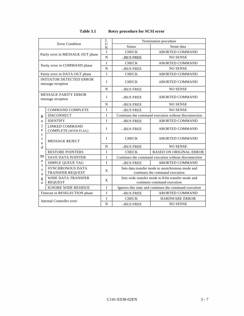
C141-E038-02EN 3 - 7
Table 3.1 Retry procedure for SCSI error
Termination procedureStatus Sense data
I CHECK ABORTED COMMANDN →BUS FREE NO SENSE
I CHECK ABORTED COMMANDN →BUS FREE NO SENSE
Parity error in DATA OUT phase I CHECK ABORTED COMMANDINITIATOR DETECTED ERRORmessage reception I CHECK ABORTED COMMAND
N →BUS FREE NO SENSEMESSAGE PARITY ERRORmessage reception I →BUS FREE ABORTED COMMAND
N →BUS FREE NO SENSECOMMAND COMPLETE I →BUS FREE NO SENSEDISCONNECT I Continues the command execution without disconnectionIDENTIFY I →BUS FREE ABORTED COMMANDLINKED COMMANDCOMPLETE (WITH FLAG) I →BUS FREE ABORTED COMMAND
MESSAGE REJECTI CHECK ABORTED COMMAND
N →BUS FREE NO SENSERESTORE POINTERS I CHECK BASED ON ORIGINAL ERRORSAVE DATA POINTER I Continues the command execution without disconnectionSIMPLE QUEUE TAG I →BUS FREE ABORTED COMMANDSYNCHRONOUS DATATRANSFER REQUEST X
Sets data transfer mode to asynchronous mode andcontinues the command execution
WIDE DATA TRANSFERREQUEST X
Sets wide transfer mode to 8-bit transfer mode andcontinues command execution
IGNORE WIDE RESIDUE I Ignores this state and continues the command executionTimeout in RESELECTION phase I →BUS FREE ABORTED COMMAND
I CHECK HARDWARE ERRORN →BUS FREE NO SENSE
Rejected
Message
Error Condition
Parity error in MESSAGE OUT phase
Parity error in COMMAND phase
Internal Controller error
LUN

C141-E038-02EN GL - 1
Glossary
Bus condition:Asynchronous operation condition used for status transition of SCSI bus. There are twotypes of bus conditions: ATTENTION and RESET conditions.
Bus phase: The name of SCSI bus state. The SCSI bus can be either in the BUS FREE,ARBITRATION, SELECTION, RESELECTION or INFORMATION TRANSFERphase. The INFORMATION TRANSFER phase is divided into subphases such asDATA IN, DATA OUT, COMMAND, STATUS, MESSAGE IN, and MESSAGE OUT.
Initiator (INIT):An SCSI device which has started up an I/O operation on the SCSI bus. The device isreferred to as INIT in this manual.
CCS: The standard SCSI logical specifications developed by the ANSI working committee.The CCS defines the functions required for direct access devices (such as disk drive).
CDB: A group of data which describes the I/O operation commands. The CDB is sent fromthe initiator to the target.
Command: An I/O operation command to the target unit (or TARG). It is referred to as the CDB.
Disconnect: Operation performed by the target to free itself from the SCSI bus and the initiatortemporarily when SCSI bus operation becomes unnecessary during commandprocessing.
Initiator: SCSI device that has initiated an input/output operation on the SCSI device. This canbe abbreviated as INIT.
Logical unit: Simple unit of equipment that can be directed to perform one I/O operation on the SCSIbus.
LUN: Logical unit number used to identify a logical unit.
LUT: A logically assigned unit which can perform I/O operations on the SCSI bus.
Message: Information that controls a series of bus phases and I/O sequence between the initiatorand the target on the SCSI bus.
Reconnect: Operation performed by the target to reconnect itself with the initiator when operationon the SCSI bus becomes necessary after disconnection.
SCSI: The standard I/O interface developed by the ANSI (X3.131-1986).
SCSI ID: A physical device address which identifies an SCSI device on the SCSI bus. Each SCSIdevice must have a unique ID. The SCSI IDs can be 0 to 7, which corresponds to onebit of the data bus.
SCSI unit: Generic name of a unit (input/output unit, I/O controller, or host adapter) connected tothe SCSI bus.
Sense code: One-byte of code attached to sense data identify the type of the detected error.
C141-E038-02ENGL - 2
Sense data: Detailed information created by the target when any error is involved in the commandtermination status. This information is transferred to report the error.
Sense key: Four-bit code attached to sense data to identify the class of the detected error.
Status: One byte of information that is transferred from a target to an initiator on termination ofeach command to indicate the command termination status.
Target: SCSI device which performs I/O initiated by an initiator. It can be abbreviated asTARG.
C141-E038-02EN IN-1
Index
1 byte length message 2-28-bit SCSI connector signal assignment 1-98-bit SCSI interface connector 1-6, 1-716-bit SCSI 1-4816-bit SCSI connector signal assignment 1-1316-bit SCSI interface connector 1-11
A
ABORT message 2-9ABORT TAG message 2-11ACK 1-5ACKNOWLEDGE 1-5ARBITRATION phase 1-32, 1-34ATN 1-5ATTENTION 1-5ATTENTION condition 1-54, 1-55, 2-4ATTENTION condition release 1-54ATTENTION condition generation 1-54ATTENTION condition response 1-54
B
BSY 1-4BUS DEVICE RESET message 2-11BUS FREE phase 1-31BUSY 1-4
C
CLEAR QUEUE message 2-11COMMAND phase 1-48COMMAND COMPLETE 3-3COMMAND COMPLETE message 2-8COMMAND PHASE parity error 3-2Command pointer 2-5Connection to an intermediate point of cable 1-19Connection to cable end 1-19CONTINUE I/O PROCESS message 2-13CONTROL/DATA 1-5C/D 1-5
D
Daisy chain connection 1-6DATA BUS 1-4Data bus width determination status 2-28DATA phase 1-48DATA IN phase 1-48DATA OUT phase 1-49DATA OUT phase parity error 3-2
Data pointer 2-5Data sequence during data transfer 2-16Data transfer rate in synchronous mode 1-50,
1-51Default data transfer mode 2-20Definition of data bus width 1-70Device connection 1-70Differential 1-3Differential input characteristics 1-76Differential output characteristics 1-75Differential output option 1-76Differential electrical condition 1-22DISCONNECT 3-3DISCONNECT message 2-9Disconnect Privilege 2-15Drive circuit 1-22, 1-23Driver protection circuit 1-24
E
Effective period of data transfer mode 2-19Error recovery control 3-6Error status 3-1Establishment of I/O operation path 2-5EXTENDED message list 2-4
F
Factory default setting 3-10Failure prediction capability flag 5-54Fast-2 synchronous data transfer 1-47Feature register 5-9, 5-34Feature register function 5-49Feature register value 5-49Features 1-1Filter, air 4-2Filter, breather 4-2Filter, circulation 2-3, 4-2Flag, failure prediction capability 5-54Flag, status 5-53Fluctuation, current 1-7Format, servo frame 4-17Format of data, device attribute value 5-51Format of data, insurance failure threshold
value 5-52Format of device attribute value data 5-51Format of insurance failure threshold value
data 5-52Format parameter data format 7-2FORMAT TRACK 5-38
IN-2 C141-E038-02EN
FORMAT TRACK command 7-1FORMAT TRACK command execution
procedure 7-2Frame 3-3Frequency characteristics of programmable
filter 4-11Full hit 6-19Function and performance 1-1
G
Gray code 4-18Guard band, inner 4-17Guard band, outer 4-17
H
HEAD of QUEUE TAG message 2-14
I
IDD synchronous mode transfer function 2-19IDD wide mode transfer function 2-28IDENTIFY 3-3IDENTIFY message 2-15, 3-5INFORMATION TRANSFER phase 1-40INFORMATION TRANSFER PHASE
identification 1-6INIT 1-1INIT initiation message exchange procedure 2-17INIT-to-TARG transfer 1-42, 1-45Internal controller error 3-5Initiator 1-1INITIATOR DETECTED ERROR message 2-9INITIATOR DETECTED ERROR message
reception 3-3INPUT/OUTPUT 1-5Interface cable 1-18Interface connector 1-6Interface signal 1-3Interface cable connection 1-19Issue of synchronous transfer request 2-5I/O 1-5
J
Jumper location 3-9Jumper setting 3-9
L
LINKED COMMAND COMPLETE message2-10
LINKED COMMAND COMPLETE WITHFLAG message 2-11
LINKED COMMAND COMPLETE (WITHFLAG) 3-3
LUN 1-2
M
MESSAGE 1-5MESSAGE phase 1-51MESSAGE IN phase 1-51MESSAGE OUT phase 1-51MESSAGE OUT phase parity error 3-1MESSAGE PARITY ERROR message 2-10MESSAGE PARITY ERROR message
reception 3-2MESSAGE REJECT 3-3MESSAGE REJECT message 2-10MSG 1-5
N
Negate current 1-73Negate voltage 1-73NO OPERATION message 2-10
O
ORDERED QUEUE TAG message 2-14
P
PAD 4-18Parameter 5-14, 5-62Parameter, default 6-6Partially hit 6-20Password, master 5-61Password, user 5-61Physical interface 5-2PIO data transfer 5-71PIO Mode 4 2-3Positioning error 1-10Power amplifier 4-16Power commands 6-10Power-on 5-75Power on/off sequence 1-7Power-on sequence 4-5Power on timing 5-75Power requirement 1-5Power save 6-8Power save mode 1-2, 6-8Power supply connector 3-9Power supply for terminating resistor 1-27PreAMP 4-9Procedure, FORMAT TRACK command
execution 7-2Processing, command 4-8Processing, sector slip 6-11
C141-E038-02EN IN-3
Product number 1-5Programmable filter 4-11Protocol, command 5-64Protocol, DMA data transfer 5-70Protocol, Read Sector(s) command 5-65Protocol, WRITE SECTOR(S) command 5-67Protocol for command abort 5-66Protocol for command execution without data
transfer 5-68
Q
QUEUE TAG message 2-14
R
Receiver circuit 1-22, 1-23REQ 1-5REQUEST 1-5RESELECTION phase 1-38, 1-39RESELECTION phase retry processing setting
1-53RESET 1-5RESET condition 1-56, 1-57Response sequence 1-36, 1-38RESTORE POINTERS message 2-8RST 1-5
S
SAVE DATA POINTER 3-4SAVE DATA POINTER message 2-8SCAM 1-65SCAM initiator 1-65SCAM operation 1-65SCSI system configuration 1-2SCSI bus 1-1SCSI pointer 2-5SCSI pointer concept 2-7SCSI message 2-1SCSI ID 1-4SCSI ID classification 1-66SCSI ID assignment 1-66SCSI error retry processing 3-7SCSI terminating circuit 1-20, 1-22SCSI-3, Fast-20 standard 1-70SEL 1-5SELECT 1-5SELECTION phase 1-35, 1-37Signal driving source 1-27Signal driving condition 1-26Signal driving method 1-26Signal status value 1-26Signal status valueSlave SCAM initiator 1-24
SIMPLE QUEUE TAG 3-4SIMPLE QUEUE TAG message 2-14Single-ended 1-3Start sequence 1-35, 1-38Status definition of data bus width 2-26STATUS phase 1-51Status pointer 2-5Switching of data bus transfer direction 1-53SYNCHRONOUS DATA TRANSFER
REQUEST 3-4SYNCHRONOUS DATA TRANSFER
REQUEST message 2-16Synchronous mode transfer 1-44, 1-46Synchronous mode transfer parameter 1-50System configuration 1-1
T
TARG 1-1TARGET TRANSFER DISABLE message 2-13Target 1-1TERMINATE I/O PROCESS message 2-12Terminating resistor circuit 1-22, 1-23Termination of differential devices 1-75Time monitor function 1-53Timing standard 1-28Timing condition 1-28Timeout processing 1-37, 1-39Transfer from TARG to INIT 1-41Transfer from INIT to TARG 1-45Transfer mode 2-20Transfer mode selection status 2-20Transfer mode selection 2-21, 2-23Transfer mode selection request 2-21, 2-24Transfer mode status definition 2-20Twisted-pair cable 1-18
U
Ultra-SCSI 1-70
V
VCM 4-2VCM current sense resistor (CSR) 4-16Vibration 1-9Viterbi detection circuit 4-12Voice coil motor 4-2
W
WIDE DATA TRANSFER REQUEST 3-4WIDE DATA TRANSFER REQUEST
message 2-26

C141-E038-02EN AB - 1
A
ACK ACKnowledgeATN ATenTionAWG American Wire Gauge
B
BSY BuSY
C
C/D Control/DataCCS Common Command SetCDB Command Descriptor Block
D
DB Data BusDBP Data Bus ParityDC Direct Current
E
EIA Engineering Industries Association
G
GND GrouND
I
I/O Input/OutputID IDentifierIDD Intelligent Disk DriveINIT INITiatorISO International Standardization
Organization
L
LSB Least Significant ByteLUN Logical Unit Number
M
MSB Most Significant ByteMSG MeSeaGe
O
OEM Original Equipment Manufacturer
R
REQ REQuestRST ReSeT
S
SCSI Small Computer System InterfaceSDTR Synchronous Data Transfer RequestSEL SELect
T
TARG TARGetTRM TeRMinator
W
WDTR Wide Data Transfer Request
Abbreviation
FUJITSU LIMITEDOEM Marketing4-1-1, Kamikodanaka, Nakahara-Ku, Kawasaki,211-88, JapanTEL: 044-754-8632FAX: 044-754-8634
FUJITSU COMPUTER PRODUCTS OF AMERICA, INC.2904 Orchard Parkway, San Jose,California 95134-2009, U.S.A.TEL: 1-408-432-6333FAX: 1-408-432-3908
FUJITSU CANADA INC.2800 Matheson Blvd. East, Mississauga, Toronto,Ontario L4W 4X5, CANADATEL: 1-905-602-5454FAX: 1-905-602-5457
FUJITSU EUROPE LIMITED2, Longwalk Road, Stockley Park, Uxbridge,Middlesex UB11 1AB, ENGLANDTEL: 44-81-573-4444FAX: 44-81-573-2643
FUJITSU DEUTSCHLAND GmbHFrankfurter Ring 211, 80807 München, GERMANYTEL: 49-89-323780FAX: 49-89-32378100
FUJITSU NORDIC ABKung Hans Väg, S-191 76 Sollentura, SWEDENTEL: 46-(0)8-6266000FAX: 46-8-626-6010
FUJITSU ITALIA S.p.A.Via Meichiorre Gioia, 8, 20124 Milano, ITALYTEL: 39-2-63651FAX: 39-2-6572257
FUJITSU FRANCE S.A.Batiment Aristote, rue Olof Palme-94006,Créteil cedex, FRANCETEL: 33-1-45-13-16-16FAX: 33-1-43-99-07-00
FUJITSU ESPAÑA S.A.C/ Almagro 40, 28010 Madrid, SPAINTEL: 34-1-581-8100FAX: 34-1-581-8125
FUJITSU AUSTRALIA LIMITED475 Victoria Avenue, Chatswood, 2067 N.S.W, AUSTRALIATEL: 61-2-410-4555FAX: 61-2-411-8603, 8362
FUJITSU HONG KONG LIMITEDRoom 2521, Sun Hung Kai Centre, Harbour Road 30, HONGHONGTEL: 852-827-5780FAX: 852-827-4724
FUJITSU KOREA LIMITED6th Floor, Duk-Heung Bldg., 1328-10, Seocho-Dong, Seocho-Ku,Seoul, KOREATEL: 82-2-739-3281FAX: 82-2-739-3294
FUJITSU (SINGAPORE) PTE. LTD75 Science Park Drive, #02-06 CINTECH II,Singapore 0511, REPUBLIC OF SINGAPORETEL: 65-777-6577FAX: 65-777-8794
FUJITSU TAIWAN LTD.8F, Hun Tai Center Bldg., 170 Tun Hwa N. Rd.,1st Sec., Taipei, TAIWAN R.O.CTEL: 886-2-545-7700FAX: 886-2-717-4644
10
Comments concerning this manual can be directed to one of the following addresses:

FUJITSU LIMITED
Thank you for your interest. Please send this sheet to one of the addresses in the left page.
Reader Comment FormWe would appreciate your comments and suggestions for improving this publication.
Publication No. Rev. Letter Title Current Date
How did you use this publication? Is the material presented effectively?
What is your overall rating of this publication? What is your occupation?
Your other comments may be entered here. Please be specific and give page,paragraph and line number references where applicable.
Your Name & Return Address
Sales
OperatingInstalling
Maintaining
Learning
Reference
Fair
Poor
Very Good
GoodVery Poor
Fullycovered
WellIllustrated
WellOrganized
Clean