Embed Size (px)
Citation preview
NASA TechniCal Memorandum 102375
Modeling of Power ElectronicSystems With EMTP ......
Kwa-Sur Tam .....
Virginia Polytechnic Institute and State UniversiO'
Blacksburg, Virginia
and
Narayan V. DravidLewis Research Center
Cleveland, Ohio
(NASA-TM-102375) MOOELING OF POWER
ELECTRONIC SYSTEMS WITH EMTP (NASA) 10 pCSCL 12R
N90-14060
Unclas
G3/o6 0252599
5f:_
December 1989
https://ntrs.nasa.gov/search.jsp?R=19900004744 2018-05-27T19:32:24+00:00Z

MODELING OF POWER ELECTRONIC SYSTEMS WITH EMTP
Kwa-Sur Tam, Member
Virginia Polytechnic Instituteand State University
Blacksburg, VA, 24061
ABSTRACT
In view of the potential impact of powerelectronics on power systems, there is need for acomputer modeling�analysis tool to perform simulationstudies on power systems with power electroniccomponents as well as to educate engineering studentsabout such systems. This paper describes thesuccessful modeling of the major power electroniccomponents of the NASA Space Station FreedomElectric Power System, EPS, with EMTP(ElectroMagnetic Transients Program) anddemonstrates that EMTP can serve as a very usefultool for teaching, design, analysis, and research in thearea of power systems with power electroniccomponents. The paper describes EMTP modeling ofpower electronic circuits and presents simulationresults.
1. INTRODUCTION
With the advent of semiconductor technology,power electronic circuits and systems will play anincreasingly significant role in electric power systems.Power electronic systems such as high voltage directcurrent (HVDC) transmission systems and static varcompensation (SVC) systems have already beeninstalled in some power systems to enhance electricpower transmission and to improve the overall systemperformance Other examples include powerconditioning units that connect alternative energysources (e.g., photovoltaic and wind energy) to utilitypower systems, motor drive systems for industrialapplications, utility interconnection to energy storagesystems (e.g., battery, fuel cells, superconductingmagnetic energy storage), etc. Besides improvementand innovative uses of existing devices and systems,there are many opportunities for developing newdevices, systems and applications.
In view of the potential impact of powerelectronics on power systems, there is need for acomputer modeling/analysis tool to perform simulationstudies of power systems with power electroniccomponents. Such a simulation tool could be used tostudy the operation of individual subsystems and theirinteractions, to investigate various system operationand design concepts, to analyze and compare differentcontrol and protection strategies, to examine theimpact of undesirable effects such as harmonicdistortions, to investigate potential problems such asresonance, etc.
The National Aeronautics and SpaceAdministration (NASA) is undertaking thedevelopment of Space Station Freedom, a mannedbase that would remain in low earth orbit for an
Narayan V. Dravid, Senior Member
National Aeronautic and Space AdministrationLewis Research Center
Cleveland, OH, 44135
indefinite length of time, for scientific, technological,and commercial purposes. NASA Lewis ResearchCenter is responsible for the design, development andfabrication of the Space Station Electric Power System(EPS). Among the technologies under investigation isa 20 kHz single phase, 440V, power management anddistribution (PMAD) system . The PMAD system isdesigned to convert power from the solar-based energysources (photovoltaic/solar dynamic) to 20 kHz fortransmission and to distribute it to various types ofcustomer loads, both dc and variable frequency ac.The initial system capacity is 75 kW. The system isplanned to grow up to 300 kW in subsequent phases.Although operated at a much higher frequency, theEPS resembles a terrestrial utility power system (60 Hz)in many respects.
NASA Lewis Research Center has built a powersystem facility for testing the hardware and software tobe developed for the EPS. Modeling capability forsimulation studies is also under development Apreliminary study has been performed to investigate thefeasibility and appropriateness of using EMTP(ElectroMagnetics Transients Program) [1] for themodeling of EPS with special emphasis on powerelectronic devices. Results of this study are describedin this paper.
The objective of this paper is to demonstratethat EMTP can be used as a tool to model powerelectronic components (including high frequencyoperation) and their interactions wire the powersystem. Engineers can use EMTP for simulation ofpower electronic systems while educators can also use itas a teaching tool for such systems. New challengesassociated with power electronics and new applicationssuch as space power systems could stimulate moreinterests among students to study power systems.
A brief overview of EMTP is provided inSection 2. The modeling of major power electroniccomponents in the EPS is described in Section 3.Applications of EMTP are discussed in Section 4.Conclusions are presented in Section 5.
2. BRIEF OVERVIEW OF EMTP
EMTP is a well-known network simulationsoftware tool for power system simulation studies, usedextensively by utility engineers. Presently, versions ofEMTP are available for a variety of computersincluding personal computers [2,3]. EMTP continuesto be updated with new features as need arises,
The theoretical basis of EMTP modeling isexplained in [1]. To model a power system, an EMTPuser assigns a name to each node of the network andspecifies how the nodes are connected. Models of avariety of power system components are available in

EMTP. Alternatively,the usermaysetupa modelofhisown device.
Control systems are modeled by using the TACS(Transient Analysis of Control Systems) program ofEMTP. During each time step, voltage, current, orother data measured from the power system are usedby the control system to determine appropriate controlactions (e.g., turning switches on/off ), which are,then, fed back to the power system for execution.Interaction between the power system and its controlsystem can be simulated accurately.
Initially, TACS was developed to model theHVDC converter control system and the resultingsimulation results were validated against field data [4].EMTP has also been used to simulate the operation ofstatic vat compensators. However, modeling of otherpower electronic circuits using EMTP is not widelyreported. The modeling of two power electroniccircuits, Which are being considered for the EPS, ispresented in this paper. One of the circuits is aphase-angle-controlled (PAC) resonant inverter thatuses thyristors and the other is apulse-width-modulated (PWM) resonant inverter thatuses transistors. Because of the increasing popularityof resonant-mode power supplies [5], these resultshave future applications. Also, the same modelingtechnique can be applied to other types of powerelectronic circuits.
3. MODELING OF EPS POWER ELECTRONIC
COMPONENTS
Although the configuration of the EPS is not yetfinal, NASA Lewis Research Center has assembled apower management and distribution (PMAD) systemhardware test bed to support the design anddevelopment of EPS where system design issues such assystem protection, control, and load management willbe addressed. A simplified schematic diagram of the
Line Resistance Inductance Capacitance(ohm) (mH) (/aF)
L1 0.0305 0.000171 0.05016L2 0.0230 0.000129 0.03784L3 0.0203 0.000114 0.03344L4 0.0728 0.000408 0.11968
Table 1. Line Data for the 20 kHz PMAD test bed
PMAD test bed is shown in Figure 1.DC power fromthe photovoltaic arrays is converted to 20 kHz ac bythe main inverter unit (MIU), which is connected tobus 1 of a 4-bus, 4-line power system. The 20 kHztransmission cable, designed to have low inductance,consists of flat foil conductors with dielectric coating.Line data for this system are given in Table 1.
Because these lines are short (less than 150feet), NASA studies indicate that a single "n'-model issufficient for line representation for most of thesimulation studies.
A major component of the PMAD system is theMIU. Two candidate circuits are currently beingconsidered for the MIU. The first is a PAC circuit
ARRAYS LI
Figure 1. A simplified schematic diagram ofthe PMAD test bed
being developed by General Dynamics while thesecond is a PWM circuit being developed by TRW.
A. Phase-angle-controlled (PAC) MIU
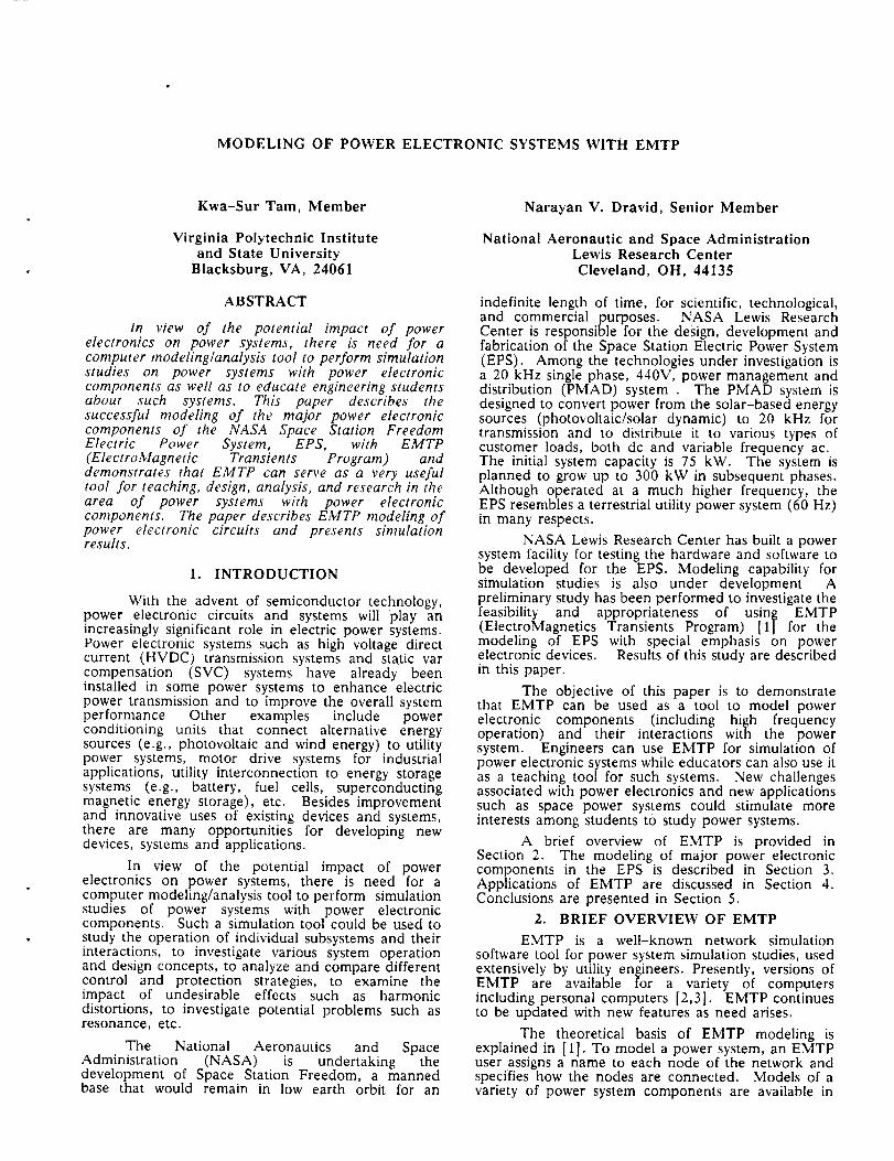
The basic component of this MIU is a dc/acresonant inverter. Figure 2 shows the schematicdiagram of this inverter, known as the Maphaminverter [6], wherein the basic resonant circuit isformed by the inductors (L) and the capacitor (C).However, the connected load across the capacitor alsoaffects the resonant circuit. The resonance frequency,fr, is determined by the values of L, C, and the load.The operating frequency, fo, of the output voltageacross C is determined by the gate firing frequency ofthe thyristors, provided that the ratio, fr/fo, is greaterthan unity. This ratio influences the performance ofthe circuit in terms of efficiency, harmonic distortion,and voltage regulation and is an important designparameter.
The steady-state operation of this circuit isdescribed as follows:
Mode 1 : Thyristors Q1 and Q2 are turned on andestablish a resonant circuit ; current flowsfrom the dc source to the capacitorthrough Q1 and Q2 and charges thecapacitor in the positive direction;currents in diodes D3 and D4 decrease tozero.
Mode 2: At the end of half of the resonanceperiod, current reverses direction andflows from the capacitor to the dc sourcethrough diodes DI and D2 ; thyristors QIand Q2 are turned off.
Mode 3 : Thyristors Q3 and Q4 are turned on andestablish a resonant circuit ; current flowsfrom the dc source to the-capacitor
throug.h Q3 and Q4 and charges thecapamtor in the negative direction ;currents in diodes D1 and D2 decrease tozero.
Mode 4: At the end of half of the resonanceperiod, current reverses direction andflows from the capacitor to the dc sourcethrough diodes D3 and D4 ; thyristors Q3and Q4 are turned off.
-I- Ol Ol
oc 'ff;
t T+cit'- -INPUT
L L
,L OUTPUT
o
_.Q4
_Q2
Figure 2. Mapham Inverter
The operation of the Mapham inverter wassimulated with EMTP and the results are shown in
Figure 3. These results are consistent with those
obtained experimentally. For this study, the operating
frequency was 20 kHz and the ratio, fr/fo, is about
1.4. The electric network portion of this circuit wasmodeled with existing EMTP features. EMTP also
offers models for thyristors and diodes while switch
characteristics such as holding current, ignition voltage,
and deionization time can be specified. Snubber
circuits were also included in the simulation. The gate
firing pulses for the thyristors were generated usingTACS.
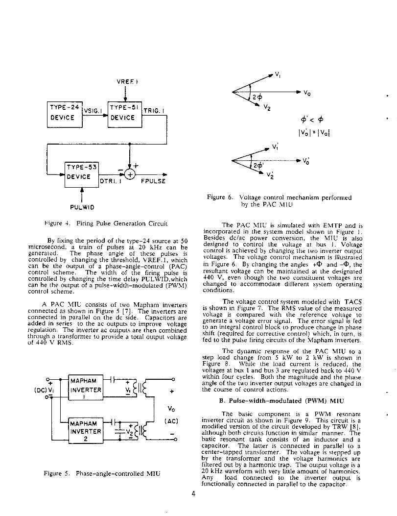
Figure 4 shows the firing pulse generation circuitimplemented with TACS. The type-24 device is a
signal source generating a periodic sawtooth waveform.
Like the other TACS devices, this device is uniquelyidentified by the name of its output, VSIG. 1, as
defined by the user. VSIG. I is the driving signal for a
type-51 device, a relay-operated switch. The type-51device is normally open and its output, TRIG. 1 is zero.
When the driving signal VSIG. 1 is greater than or equalto a user-controlled threshold, VREF. I, TRIG. 1
changes to unity.
TRIG. 1 is fed to a pulse shaping circuit. DTRI. 1,
output of the type-53 (transport delay) device, differs
from its input TRIG. l by a user-controlled time delayPULWID. By subtracting DTRI. 1 from TRIG. 1 a pulsewith a controlled width can be obtained. FPULSE is
the firing pulse that controls the operation of athyristor. Since SCRs respond only to positive gate
signals, the negative portion of FPULSE does not affect
the operation of the circuit and, if desired, may be
filtered away by passing FPULSE through a limiter withthe lower limit set at zero.
ti [hi
*o
50 "
,,
0 •
1,
50 ,,
0 .
tO ..
0 ,
-10
"n'l,"v ru]
300 .i
0 ,
ti,
-300 ..
200
Figure 3.
(a)
QI
Thyristor gate
....Q3 __QI
firing pulses
....Q3
(b)
/%I
\\
Current through Q[ and Dt
A
,\!
\ / \ !
,i,
(c) Current through Q3 and D3
; \ ; './ ,, / \/
\ /,j ',,
(d) Output current
/% ,/'\/ 2/ X,
) Output voltage
/--. /I--,X
I1 _x ¢
,/ \ / ",\
250 _ :,',l
Time (microsecond)
Steady State operation of the MaphamInverter
VREE I
TYPE-51
DEVICE TRIG. I
TYPE-53 I
Io,,,.,
PULWID
FPULSE
Figure 4. Firing Pulse Generation Circuit
By fixing the period of the type-24 source at 50microsecond, a train of pulses at 20 kHz can begenerated. The phase angle of these pulses iscontrolled by changing the threshold, VREF. 1, whichcan be the output of a phase-angle-control (PAC)control scheme. The width of the firing pulse iscontrolled by changing the time delay PULWID,whichcan be the output of a pulse-width-modulated (PWM)control scheme.
A PAC MIU consists of two Mapham invertersconnected as shown in Figure 5 [7]. The inverters areconnected in parallel on the dc side. Capacitors areadded in series to the ac outputs to improve voltageregulation. The inverter ac outputs are then combinedthrough a transformer to provide a total output voltageof 440 V RMS.
4-
(DC) V_
_ MAPHAM __V_I _._ oVo
I -o
Figure 5. Phase-angle-controlled MIU
!
Vo
_'<_IIVol:lVol
Figure 6. Voltage control mechanism performedby the PAC MIU
4
The PAC MIU is simulated with EMTP and is
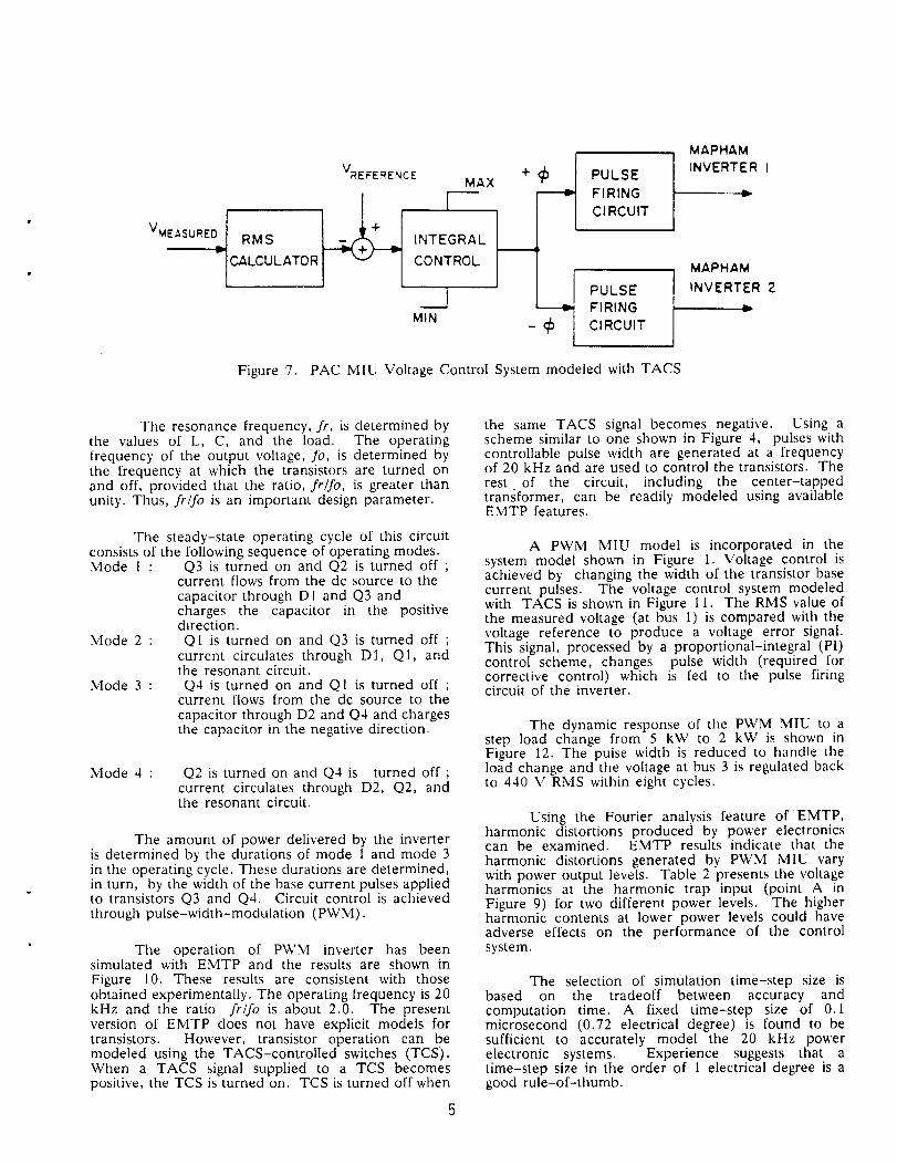
incorporated in the system model shown in Figure 1.Besides dc/ac power conversion, the MIU is alsodesigned to control the voltage at bus 1. Voltagecontrol is achieved by changing the two inverter outputvoltages. The voltage control mechanism is illustratedin Figure 6. By changing the angles +_ and -_, theresultant voltage can be maintained at the designated440 V, even though the two constituent voltages arechanged to accommodate different system operatingconditions.
The voltage control system modeled with TACSis shown in Figure 7. The RMS value of the measuredvoltage is compared with the reference voltage togenerate a voltage error signal. The error signal is fedto an integral control block to produce change in phaseshift (required for corrective control) which, in turn, isfed to the pulse firing circuits of the Mapham inverters.
The dynamic response of the PAC MIU to astep load change from 5 kW to 2 kW is shown inFigure 8, While the load current is reduced, thevoltages at bus 1 and bus 3 are regulated back to 440 Vwithin four cycles. Both the magnitude and the phaseangle of the two inverter output voltages are changed inthe course of control actions.
B. Pulse-width-modulated (PWM) MIU
The basic component is a PWM resonantinverter circuit as shown in Figure 9. This circuit is amodified version of the circuit developed by TRW [8],although both circuits function in similar manner. Thebasic resonant tank consists of an inductor and acapacitor. The latter is connected in parallel to acenter-tapped transformer. The voltage is stepped upby the transformer and the voltage harmonics arefiltered out by a harmonic trap. The output voltage is a20 kHz waveform with very little amount of harmonics.Any load connected to the inverter output isfunctionally connected in parallel to the capacitor.
VME_SLJRED[ RMS
:'tCALCU LATOR
VREFERENCEMAX
IINTEGRAL
CONTROL
PULSE
FIRING
CIRCUIT
____J ._ PULSEFIRING
MIN - CIRCUIT
Figure 7. PAC MIU Voltage Control System modeled with TACS
MAPHAM
INVERTER t
MAPHAM
INVERTER 2
The resonance frequency, Jr, is determined bythe values of L, C, and the load. The operatingfrequency of the output voltage, fo, is determined bythe frequency at which the transistors are turned onand off, provided that the ratio, fr/fo, is greater thanunity. Thus, fr/fo is an important design parameter.
The steady-state operating cycle of this circuitconsists of the following sequence of operating modes.Mode I : Q3 is turned on and Q2 is turned off ;
current flows from the dc source to the
capacitor through D1 and Q3 andcharges the capacitor in the positivedirection.
Mode 2 : QI is turned on and Q3 is turned off ;current circulates through D J, Q1, andthe resonant circuit.
Mode 3 : Q4 is turned on and Q I is turned off ;current flows from the dc source to the
capacitor through D2 and Q4 and chargesthe capacitor in the negative direction.
Mode 4 : Q2 is turned on and Q4 is turned off ;current circulates through D2, Q2, andthe resonant circuit.
The amount of power delivered by the inverteris determined by the durations of mode 1 and mode 3in the operating cycle. These durations are determined,in turn, by the width of the base current pulses appliedto transistors Q3 and Q4. Circuit control is achievedthrough pulse-width-modulation (PWM).
The operation of PWM inverter has beensimulated with EMTP and the results are shown inFigure 10. These results are consistent with thoseobtained experimentally. The operating frequency is 20kHz and the ratio fr/fo is about 2.0. The presentversion of EMTP does not have explicit models fortransistors. However, transistor operation can bemodeled using the TACS-controlled switches (TCS).When a TACS signal supplied to a TCS becomespositive, the TCS is turned on. TCS is turned off when
the same TACS signal becomes negative. Using ascheme similar to one shown in Figure 4, pulses withcontrollable pulse width are generated at a frequencyof 20 kHz and are used to control the transistors. Therest of the circuit, including the center-tappedtransformer, can be readily modeled using availableEMTP features.
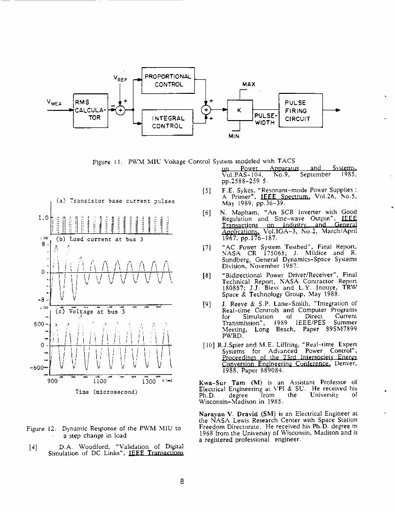
A PWM MIU model is incorporated in thesystem model shown in Figure 1. Voltage control isachieved by changing the width of the transistor basecurrent pulses. The voltage control system modeledwith TACS is shown in Figure 11. The RMS value ofthe measured voltage (at bus 1) is compared with thevoltage reference to produce a voltage error signal.This signal, processed by a proportional-integral (PI)control scheme, changes pulse width (required forcorrective control) which is fed to the pulse firingcircuit of the inverter.
The dynamic response of the PWM MIU to astep load change from 5 kW to 2 kW is shown inFigure 12. The pulse width is reduced to handle theload change and the voltage at bus 3 is regulated backto 440 V RMS within eight cycles.
Using the Fourier analysis feature of EMTP,harmonic distortions produced by power electronicscan be examined. EMTP results indicate that theharmonic distortions generated by PWM MIU varywith power output levels. Table 2 presents the voltageharmonics at the harmonic trap input (point A inFigure 9) for two different power levels. The higherharmonic contents at lower power levels could haveadverse effects on the performance of the controlsystem.
The selection of simulation time-step size isbased on the tradeoff between accuracy andcomputation time. A fixed time-step size of 0.1microsecond (0.72 electrical degree) is found to besufficient to accurately model the 20 kHz powerelectronic systems. Experience suggests that atime-step size in the order of 1 electrical degree is agood rule-of-thumb.

it,, (a) Load current at bus 3
o //i,i aa i) !/vvvv,,-8 b/
'"[ (b) Voltage at bus 3
600... I " "^ ? _ n. .."_; ', i i i \ . :. ; , •" ' , ' ', ; , i ' '
0:j!/!/ i/ !/ :! i/
,,°
600 ...
..o
O.
600:::[-- ... !
(c) Voltage at bus 1
, / :
j "; iL,
' _ ,; ;
,, : _ i . .w ;%/
v [Vl
,,.[ (d) Output voltage of inverter 1l f_ A _ _, n r,
2oo..,:,, ,,, , <_ !,, ,\o:I/i ii /i /i ii /i.,.li \J ',_ i! il iJ
v V V v,gl
200 :'-
0
-200 .....lwo,
..... 4"00 ..... "'300 500 t_,
Time (microsecond)
°.i ,,* .,
(e) Output voltage o_ inverter 2
vvTVVV
Figure 8. Dynamic Response of the PAC MIU to
a step change of load
4. APPLICATIONS OF EMTP
A
HARMONICTRAP
LL Oi
_ r-y-,
_Li=l+
QI
1L. _,
Q2
,y,-+
OC INPUT
o+ AC
OUTPUT
o
02
Q4
Figure 9. Pulse-width-modulated resonant inverter
With its present features, EMTP can be used to
support the following modeling activities, which, in
turn, could be used for purposes such as teaching,design, analysis, research, etc.
1. Simulation of steady-state and transientbehavior.
Good understanding of the behavior of
components, circuits, and systems in different
situations may be gained using EMTP simulations.
2. Experimentation with new ideas andevaluation of alternatives.
Harmonic 5 kW 2 kW
number (%) (%)
0 0.2 0.9
1 100.0 100.0
3 6.4 7.2
5 0.8 2.0
7 0.4 0.8
9 0.4 0.4
11 0.2 0.313 0.1 0.2
Table 2. Voltage Harmonic levels at the harmonic
trap input at two power levels

Transistor base current pulses
.....Q4 Q3 .....Q4
160,..I
0'
(b) Resonant tank inductor current
v [U1
300 '"
O.
-300 ,-
(c) Resonant tank capacitor voltage
/ \,
v [Ul
600 '"
0 •
-600 ....
(d) Output voltage
/<,/ '\ / \/ V U(e) Output current
C"\
400 450 ,c.*
Time (microsecond)
Figure 10. Steady State operation of PWM Inverter
EMTP simulation provides an inexpensive and
convenient method to test new ideas and to comparealternatives for system components, system structures,and control schemes. For example, an experimentalcontrol/protection scheme was developed [or the PACMIU to enhance its performance during faultconditions. Upon detection of a fault, the scheme willforce the two inverter voltages to be out of phase,resulting in a zero voltage at the MIU output.However, simulation indicates that this scheme requiresinverters with a much higher current rating.
3. Obtaining information on equipment ratings.
EMTP simulation can provide information onthe required ratings of various system components.For example, the blocking voltage requirement of SCRsin the PAC MIU can be determined by plotting thevoltages across the SCRs.
4. Investigation of potential problems.
EMTP simulation can be used to identifypotential problems and to study solutions. Forexample, EMTP simulation shows that the PWM MIUis vulnerable to open circuit conditions. This should betaken into consideration during the design of theprotection system.
Instead of interfacing with TACS, the systemmodeled with EMTP can be monitored, operated andcontrolled using actual control hardware and/orsoftware. Work is underway to integrate EMTP withreal-time control for enhanced simulation, controllerdesign, and on-site controller diagnostic [9]. EMTPmay also be integrated with real-timecontrol/protection expert system [10] for simulationand control verification.
5. CONCLUSIONS
This study demonstrates that power electronicsystems can be modeled with EMTP. The techniqueused to model PAC and PWM circuits can be appliedto model a wide variety of power electronic circuits.EMTP modeling is accurate and can support variousmodeling activities that are useful for teaching, design,analysis, and research associated with power systemsand power electronics. Potential areas of applicationsinclude real-time control and expert systems.
6. ACKNOWLEDGMENTS
This material is based upon work supported bythe NASA Summer Faculty Fellowship. The authorswould like to thank their colleagues at the NASA LewisResearch Center for their support and cooperation.
7. REFERENCES
[1] H.W. Domme], ELECTROMAGNETICTRANSIENTS PROGRAM REFERENCE
Bonneville Power Administration,1986.
[2] Electric Power Research Institute,ElectroMagnetic Transients Program Version2.0, Palo Alto, 1989.
[3] Alternative Transient Program, LeuvenElectromagnetic Transients Program Center,Belgium, 1987.
VMEA
VRE'F r_
PROPORTIONAL
CONTROL
INTEGRAL
CONTROL
_x
PULSE-
WIDTH
PULSE
FIRING
CIRCUIT
Figure 11. PWM MIU Voltage Control System modeled with TACS
on Power Apparatus and Systems.
4
(a) Transistor base current pulses
ri!iHi!li IiIiiIf!iJIJiII!!i_.i (b) Load current at bus 38,
°1 ;', ."
D
.i " " '" /! i_ " !'! A ";o i it it. !k t fk , ,,,
titiv,,vvvv,',1,
V V
,,°
600"
J_
O.
-600__
_l, _*,, _i ,_P, _ii ,i,i ,t, ,IN L_T'
(c) Voltage at bus 3
, ;. . . , :_ , :: /', :. ;
/TL, 'tli "_'_t/_! ii ti' 'v _i I /i tV_ ; t,/ V7
900 ii00 1300 l_,l
Time (microsecond)
Figure 12. Dynamic Response of the PWM MIU to
a step change in load
[4] D.A. Woodford, "Validation of DigitalSimulation of DC Links", IEEE Transactions
Vol.PAS- 104, No.9, September 1985,
pp.2588-259 5.
[5] F.E. Sykes, "Resonant-mode Power Supplies :
A Primer", _ Vol.26, No.5,
May 1989, pp.36-39.
[6] N. Mapham, "An SCR Inverter with GoodRegulation and Sine-wave Output", IEEETransactions on Industry and General
Applications. Vol.IGA-3, No.2, March/April
1967, pp. 176-187.
[7] "AC Power System Testbed", Final Report,NASA CR 175068; J. Mildice and R.
Sundberg, General Dynamics-Space SystemsDivision, November 1987.
[8] "Bidirectional Power Driver/Receiver", FinalTechnical Report, NASA Contractor Report180887; J.J. Biess and L.Y. lnouye, TRW
Space & Technology Group, May 1988.
[9] J. Reeve & S.P. Lane-Smith, "Integration ofReal-time Controls and Computer Programsfor Simulation of Direct Current
Transmission", 1989 IEEE/PES Summer
Meeting, Long Beach, Paper 89SM7899PWRD.
[10] R.J.Spier and M.E. Liffring, "Real-time Expert
Systems for Advanced Power Control",
Proceedings of the 23rd Intersociety EnergyConversion Engineering Conference. Denver,
1988, Paper 889084.
Kwa-Sur Tam (M) is an Assistant Professor of
Electrical Engineering at VPI & SU. He received his
Ph.D. degree from the University ofWisconsin-Madison in 1985.
Narayan V. Dravid (SM) is an Electrical Engineer atthe NASA Lewis Research Center with Space Station
Freedom Directorate. He received his Ph.D. degree in
1968 from the University of Wisconsin, Madison and is
a registered professional engineer.

Na|ional Aeronaulics andSpace Administration
1. Report No.
NASA TM-102375
4. Title and Subtitle
Modeling of Power Electronic Systems With EMTP
7. Author(s)
Kwa-Sur Tam and Narayan V. Dravid
g,
12.
Performing Organization Name and Address
National Aeronautics and Space AdministrationLewis Research Center
Cleveland, Ohio 44135-3191
Sponsoring Agency Name and Address
National Aeronautics and Space Administration
Washington, D.C. 20546-0001
3. Recipient's Catalog No.
5. Report Date
December 1989
6. Performing Organization Code
8. Performing Organization Report No.
E-5109
Report Documentation Page
2. Government Accession No.
10. Work Unit No.
474-42-10
11. Contract or Grant No.
13. Type of Report and Period Covered
Technical Memorandum
14. Sponsoring Agency Code
15. Supplementary Notes
Kwa-Sur Tam, Virginia Polytechnic Institute and State University, Blacksburg, Virginia; Narayan V. Dravid,NASA Lewis Research Center.
16. Abstract
In view of the potential impact of power electronics on power systems, there is need for a computer modeling/
analysis tool to perform simulation studies on power systems with power electronic components as well as to
educate engineering students about such systems. This paper describes the successful modeling of the major power
electronic components of the NASA Space Station Freedom Electric Power System, EPS, with EMTP
(ElectroMagnetic Transients Program) and demonstrates that EMTP can serve as a very useful tool for teaching,
design, analysis, and research in the area of power systems with power electronic components. The paper describes
EMTP modeling of power electronic circuits and presents simulation results.
17. Key Words (Suggested by Author(s))
Education; Simulation; DC/AC resonant inverters; PWM;
Harmonics; Transients; Operation; Control
18. Distribution Statement
Unclassified- Unlimited
Subject Category 66
19. Security Classif. (of this report) 20. Security Classif. (of this page) 21. No of pages
Unclassified Unclassified 10
NASAFORM1626OCT86 *For sale by the National Technical Information Service, Springfield, Virginia 22161
22. Price*
A02


![TRANSMISSION LINE MODELING FOR REAL-TIME … · is a reformulation of the EMTP-RV model WB Line (based on the Universal Model [3]), in-line with the ... 3 EMTP-RV and transmission](https://img.pdfslide.us/doc/110x75/5afc554a7f8b9aa34d8bf3f9/transmission-line-modeling-for-real-time-a-reformulation-of-the-emtp-rv-model.jpg)