Embed Size (px)
Citation preview
Optics Communications 482 (2021) 126614
MZa
b
A
KP4PI
1
cgiidtdamwrp
cpHddhsRsoP
hRA0
Contents lists available at ScienceDirect
Optics Communications
journal homepage: www.elsevier.com/locate/optcom
ode-resolved analysis of a planar multi-layer plasmonic nanolaserihad Azad a, Md. Shofiqul Islam b, Muhammad Anisuzzaman Talukder a,∗
Department of Electrical and Electronic Engineering, Bangladesh University of Engineering and Technology, Dhaka 1205, BangladeshDepartment of Electrical and Computer Engineering, Faculty of Engineering, King Abdulaziz University, PO Box 80204, Jeddah 21589, Saudi Arabia
R T I C L E I N F O
eywords:lasmonic nanolaser-level 2-electron modelhotonic crystalsR-140 dye molecules
A B S T R A C T
Plasmonic nanolasers (PNLs) have attracted much attention in recent years due to their light-trappingcapabilities beyond the diffraction limit. However, the physics that underpins the lasing action in suchdevices has not received sufficient treatment in the literature. The contribution of plasmons in PNLs needsto be understood at a granular level for designing enhanced nanoscopic lasers. In this work, we present amodal decomposition-based analysis of a planar PNL that employs a two-dimensional metallic nanohole arrayinterfaced with the gain medium. Using state-of-the-art simulation techniques, we isolate the plasmonic modethat emerges at the metal–gain medium interface interlaced with scattering modes. We present a step-by-step dispersion analysis to identify the possible modes supported by the planar PNL structure and locate theoperating point of the PNL. Furthermore, we show how the plasmonic mode regulates the lasing action, andhence, can serve as a tool for laser tunability.
. Introduction
Lasers are spatiotemporally coherent sources of light that offerompetitive applications in a wide range of industries, running theamut from consumer technology to nuclear fusion [1,2]. However,n many potential sectors, e.g., laser surgery, on-chip optical comput-ng, bio-sensing, and data storage, a compact laser with nanoscaleimensions has become a dire necessity [3]. Unfortunately, conven-ional microcavity-based lasers are diffraction-limited, i.e., the cavityimensions cannot be smaller than half of the operating wavelengthlong any one direction [4]. To overcome this intrinsic limitation, novelechanisms are being explored to compress electromagnetic energyithin subwavelength dimensions [5]. One such crucial avenue of
esearch is the introduction of metal in laser design to induce surfacelasmons.
Plasmonic modes – excited in the presence of metallic structures –ouple energy way beyond the diffraction limit. Furthermore, the am-lificatory characteristic of plasmons can mimic resonator effects [6].ence, plasmonic modes have emerged as a promising candidate foresigning nanoscale lasers. The first proof-of-principle of a PNL wasemonstrated in 2007 [7]. Since then, research interest in this fieldas witnessed a sharp rise. However, the inclusion of plasmons in laserystems comes with additional ohmic losses in the metal layer [8].esearchers have implemented heterodox strategies to exploit the manytrands of plasmons, as well as to circumvent additional losses such ashmic losses due to the inclusion of metal. From design point-of-view,NLs can be divided in the following broad categories: (1) metallic
∗ Corresponding author.E-mail address: [email protected] (M.A. Talukder).
nanowire-based PNLs, (2) metallic nanoparticle-based PNLs, and (3)metallic planar structure-based PNLs. In metallic nanowire-based PNLs,a semiconductor nanowire sits atop a metal layer, and the nanowire isoften separated from the metal layer by a nanoscale-thick insulator [9].In this design, surface plasmon polaritons (SPPs) are hybridized withphotonic or waveguide modes, which allows SPPs to traverse longerdistances with strong modal confinement [10,11].
In metallic nanoparticle-based PNLs, on the other hand, a funda-mental variant of plasmonic mode dubbed localized surface plasmon(LSP) – stationary plasmonic excitation in metallic nanoparticles – isexploited to generate lasing [12–14]. Finally, in planar interfaced PNLs,where layers of different materials are stacked one after another, plas-monic modes that emerge at the interfaces between metal and dielectricmaterials hybridize with photonic modes [4]. Plane parallel slabbingstrategy for designing nanoscale lasers has gained significant interestin PNL research due to its ability to produce higher optical outputpower compared to the other approaches. Planar interfaced PNLs cancome in variants with metallic nanostructures in the interface betweenmetal and dielectric layers for better exploitation of both plasmonic andphotonic modes [14]. Recently, a novel structure has been proposedin which a metallic nanohole array (NHA) is used with a nanoscalegain medium for enhanced directionality and efficiency [15]. A one-dimensional photonic crystal (1-D PhC) superposed on the gain mediumof the nanolaser of Ref. [15] helps to induce the coupling of stimulatedemission energy to optical Tamm plasmon polaritons (TPPs) at theinterface between the metal layer and the 1-D PhC [16]. The periodic
ttps://doi.org/10.1016/j.optcom.2020.126614eceived 21 September 2020; Received in revised form 8 November 2020; Acceptevailable online 16 November 2020030-4018/© 2020 Elsevier B.V. All rights reserved.
d 11 November 2020
Z. Azad, Md. Shofiqul Islam and M.A. Talukder Optics Communications 482 (2021) 126614
hlrtedu
nanoholes in NHA couple the TPP mode to free-space, radiative modevia extraordinary optical transmission (EOT). Planar structures havealso been shown to induce whispering-gallery modes in PNLs [17,18].
Although there has been significant progress in PNL research, acomprehensive theoretical study of the physics underpinning the lasingaction in plasmon-integrated systems is still lacking. Presumably, plas-mons are the key mechanism of a PNL. However, due to the diversity ofapproaches involved, different modes may accompany the fundamentalplasmonic mode in different designs. The spectral purity of the outputemission, tuning of emission wavelength, and far-field directionalitywill critically depend on the modes excited within the PNL cavity.Additionally, to understand the lasing mechanism so that improvedand novel PNLs can be designed and tailored for various applications,an analysis that decomposes lasing light into constituent modes thatresonate inside the nanolaser cavity and make the emission profile willbe immensely helpful.
In this work, we carry out a mode-resolved analysis of PNLs thatexploit parallel plane interfacing of metal and dielectric media. Inparticular, we analyze the PNL structure presented in Ref. [15] thathas a metallic NHA interfaced with the gain medium so that SPPsevolve at the planar metal–gain medium interface and coalesce atthe output as a radiative and spectrally coherent EOT mode. ThePNL structure proposed in Ref. [15] effectively separates the lasingemission from the pump pulse, increases the emission intensity, andmakes the far-field pattern directional. The internal physics of theproposed parallel plane PNL structure with a metallic NHA was notinvestigated in Ref. [15] and remained mostly elusive. It was assumedthat the plasmonic excitation plays a significant role in the designedPNL structure; however, a definitive link was not explored, let aloneestablished. Additionally, in the research work published in Ref. [15],we found that a few aspects of such plasmonic lasers contradict theconventional physics of laser dynamics. We explained a few thingsintuitively in Ref. [15]; however, an in-depth analysis with theoreticalmodeling and computational work that unearths the underlying physicsis crucially important for designing improved plasmonic lasers withenhanced and tailored performances.
In this work, we decompose the emission spectra at the outputand the resonating modes inside the cavity using state-of-the-art sim-ulation techniques. We calculate the dispersion relations to identifyall modes that are supported by the studied PNL structure and findout the operating point of the laser—the point of overlap betweenthe supported modes and the gain bandwidth. We show how we canexploit the SPP mode to tune the lasing spectra. By demonstratingthat the gain resonance excites plasmons and the lasing mode shiftsin response to the plasmonic mode, we have found a definitive linkbetween the excitation of plasmons and the lasing action of the studiedPNL, which may serve as a first-principles framework for understandingand designing future PNLs.
2. Nanolaser structure
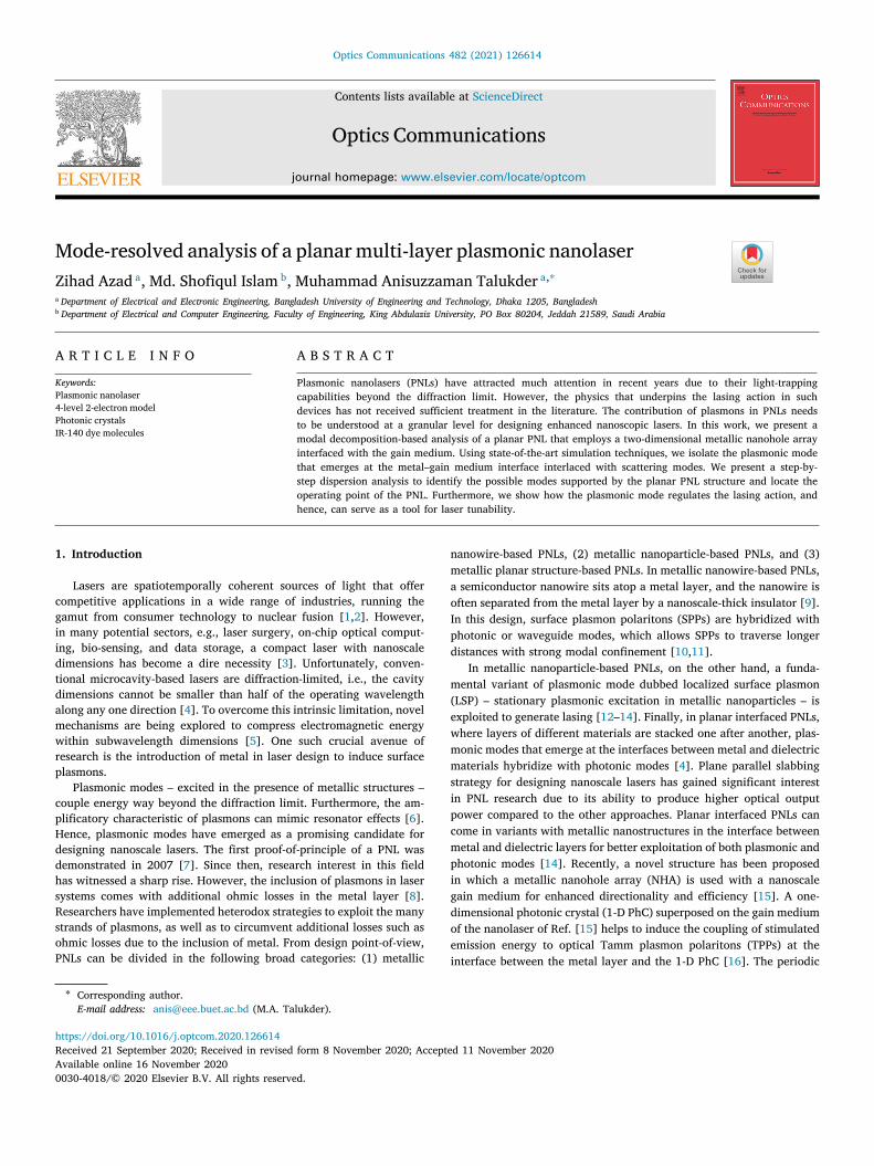
We investigate the PNL structure that was presented and discussedin Ref. [15]. In Fig. 1(a), we show a schematic diagram of the structure.A polyurethane (PU) layer spin-coated with fluorescent IR-140 dyemolecules that functions as the active medium is placed on the topof a gold layer. IR-140 dye molecules have a broad fluorescence spec-trum [19] that makes them a suitable candidate for laser gain medium,especially in widely tunable lasers. Additionally, IR-140 moleculesshow a superior photo-physical performance when they are used asan active dopant with polymers, as compared to other familiar dyemolecules such as Rhodamine 6G or pyrromethene 567 [20]. On theother hand, the use of gold as the metal layer is favored over silver andcopper. While copper is not a suitable metal for their inability to exciteSPP modes in the near-infrared regime and huge loss incurred withincopper, both gold and silver help excite strong SPP modes in the near-
infrared regime and support long propagation length for SPP modes2
Table 1Refractive indices of dielectric layers.
Material Refractive Index
TiO2 2.23MgF2 1.38PU 1.52
with a relatively less loss [21]. However, silver shows a relatively poorperformance in comparison with gold due to a lack of chemical stabilityof silver, susceptibility to surface impurities, and difficulty to growsingle-crystalline silver layers [22]. The gold layer is perforated withtwo-dimensional (2-D) square holes with subwavelength periodicity.The 1-D PhC consisting of 5 pairs of alternating TiO2 and MgF2 layersis separated from the gain medium by a comparatively thicker spacerlayer of TiO2. The alternating TiO2 and MgF2 layer thicknesses are108 nm and 165 nm, respectively. The spacer layer thickness is 200 nm,while the IR-140-doped PU gain layer is 325-nm thick. The metal layerhas a thickness of 100 nm with 170 nm × 170 nm nanoholes that havea periodicity of 350 nm in both the 𝑥- and 𝑦-directions. The refractiveindices of different dielectric materials used in the PNL structure areprovided in Table 1 [15].
The PNL structure is uniformly optically pumped from the PhC sideby a normally incident, ultra-short 40 fs plane wave pulse, centered at800 nm. We set the source intensity to 8.8 μW∕cm2. The 1-D PhC servesas a distributed Bragg reflector (DBR) to suppress the forward scatteringof the pump pulse. The layer thicknesses, as well as refractive indices,are chosen in such a way that the reflectance bandgap of the DBRcoincides with the spectrum of pump pulse centered at 790 nm [23].Fig. 1(b) presents the cross-sectional view of the structure in the x-z plane. SPPs are excited in the metal–gain medium interface, whileEOT occurs through the holes in the metal layer to create the lasingemission. In effect, the square holes in the metal layer emit sphericalwavefronts that interfere constructively in the far-field to produce ahighly directional laser beam.
3. Theoretical modeling and simulation methodology
Theoretical modeling is crucially important in understanding thephysics of plasmonic lasing at nanoscopic dimensions and designingimproved plasmonic lasers with enhanced performances. Intuitively,the gain resonance from the active medium would transfer excitonicenergy to the surface plasmons that act as nanoresonators. However,if a definite causative link between the induced plasmonic mode andthe radiative mode in a planar interfaced PNL can be established viatheoretical modeling and numerical approach, as pursued in this work,future research works in this field can be carried out in a scientificallymore rigorous way.
3.1. Active medium
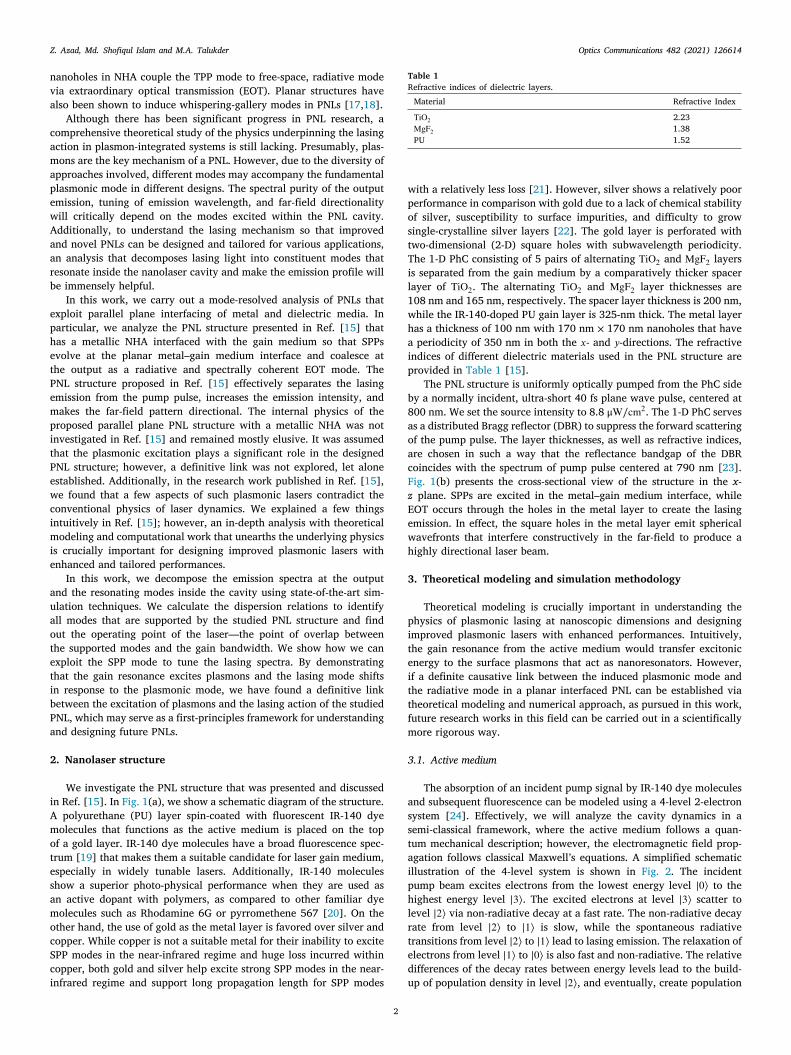
The absorption of an incident pump signal by IR-140 dye moleculesand subsequent fluorescence can be modeled using a 4-level 2-electronsystem [24]. Effectively, we will analyze the cavity dynamics in asemi-classical framework, where the active medium follows a quan-tum mechanical description; however, the electromagnetic field prop-agation follows classical Maxwell’s equations. A simplified schematicillustration of the 4-level system is shown in Fig. 2. The incidentpump beam excites electrons from the lowest energy level |0⟩ to theighest energy level |3⟩. The excited electrons at level |3⟩ scatter toevel |2⟩ via non-radiative decay at a fast rate. The non-radiative decayate from level |2⟩ to |1⟩ is slow, while the spontaneous radiativeransitions from level |2⟩ to |1⟩ lead to lasing emission. The relaxation oflectrons from level |1⟩ to |0⟩ is also fast and non-radiative. The relativeifferences of the decay rates between energy levels lead to the build-p of population density in level |2⟩, and eventually, create population
Z. Azad, Md. Shofiqul Islam and M.A. Talukder Optics Communications 482 (2021) 126614
i
T
Fig. 1. (a) Perspective view of the studied PNL structure [15]. Alternating layers of TiO2 and MgF2 form the 1-D photonic crystal. (b) Cross-sectional view of the PNL structuren the x-z plane.
T
atacr
𝜀stp
Fig. 2. Schematic diagram of a 4-level 2-electron system.
Table 2Parameter values for IR-140 dye molecules.
Parameter Value
Emission wavelength (𝜆𝑎) 870 nmEmission linewidth (𝛥𝜆𝑎) 100 nmAbsorption wavelength (𝜆𝑏) 800 nmAbsorption linewidth (𝛥𝜆𝑏) 100 nmDye concentration (𝑁density) 2 × 1024 cm−3
Polarization decay rate (𝛾𝑎 = 𝛾𝑏) 3.9 × 10¹³ s−1
Radiative decay rate (𝛾rad) 7.2 × 10⁷ s−1
Transition lifetimes (𝜏21 = 𝜏30) 1 nsTransition lifetimes (𝜏32 = 𝜏10) 10 fs
inversion between levels |1⟩ and |2⟩, which is the elemental conditionof lasing action.
In this modeling approach, the two radiative transitions betweenlevels |2⟩ and |1⟩ and between levels |0⟩ and |3⟩ are modeled as twocoupled dipole oscillators with polarizations 𝑃𝑎 and 𝑃𝑏, respectively.
he decay or dephasing rates of 𝑃 and 𝑃 are 𝛾 and 𝛾 , respectively.
𝑎 𝑏 𝑎 𝑏 E3
he governing equations for the coupled dipole oscillators are [25]
𝑑2 𝑃𝑎
𝑑𝑡2+ 𝛾𝑎
𝑑 𝑃𝑎𝑑𝑡
+ 𝜔2𝑎𝑃𝑎 =
6𝜋𝜀0𝑐3
𝜔𝑎𝜏21(𝑁2 −𝑁1)𝐸, (1a)
𝑑2 𝑃𝑏
𝑑𝑡2+ 𝛾𝑏
𝑑 𝑃𝑏𝑑𝑡
+ 𝜔2𝑏𝑃𝑏 =
6𝜋𝜀0𝑐3
𝜔𝑏𝜏30(𝑁3 −𝑁0)𝐸, (1b)
where 𝑁𝑖 is the normalized population density of level i; 𝜔𝑎 and 𝜔𝑏re the resonant frequencies of 𝑃𝑎 and 𝑃𝑏, respectively; 𝜏𝑖𝑗 is the decayime constant between levels i and j; and 𝜀0 and 𝑐 are the permittivitynd the speed of light in vacuum, respectively. The assumption of twooupled dipole oscillators leads to the following set of equations thategulates the population dynamics among the four energy levels [25]
𝑑𝑁3𝑑𝑡
= −𝑁3(1 −𝑁2)
𝜏32−
𝑁3(1 −𝑁0)𝜏30
+ 1ℏ𝜔𝑏
𝐸 ⋅𝑑 𝑃𝑏𝑑𝑡
, (2a)
𝑑𝑁2𝑑𝑡
=𝑁3(1 −𝑁2)
𝜏32−
𝑁2(1 −𝑁1)𝜏21
+ 1ℏ𝜔𝑎
𝐸 ⋅𝑑 𝑃𝑎𝑑𝑡
, (2b)
𝑑𝑁1𝑑𝑡
=𝑁2(1 −𝑁1)
𝜏21−
𝑁1(1 −𝑁0)𝜏10
− 1ℏ𝜔𝑎
𝐸 ⋅𝑑 𝑃𝑎𝑑𝑡
, (2c)
𝑑𝑁0𝑑𝑡
=𝑁3(1 −𝑁0)
𝜏30+
𝑁1(1 −𝑁0)𝜏10
− 1ℏ𝜔𝑏
𝐸 ⋅𝑑 𝑃𝑏𝑑𝑡
. (2d)
The model links Eqs. (1) and (2) to the Maxwell–Ampere law givenby [25]
𝑑 𝐸𝑑𝑡
= 1𝜀∇ × 𝐻 − 1
𝜀𝑁density
(
𝑑 𝑃𝑎𝑑𝑡
+𝑑 𝑃𝑏𝑑𝑡
)
, (3)
where 𝐸 and 𝐻 are the electric and magnetic fields, respectively, andis the permittivity of the background material. Eqs. (1)–(3) form a
elf-consistent set of equations that are solved by the finite-differenceime-domain (FDTD) numerical technique to find out the time-resolvedopulation evolution of the four quantum levels. In this work, we solveqs. (1)–(3) using a full-field vectorial three-dimensional (3-D) FDTD
Z. Azad, Md. Shofiqul Islam and M.A. Talukder Optics Communications 482 (2021) 126614
dto
tw𝑥ltfp𝑧PldhstT
3
u
𝛼
up
3
bwacibttoosm
t
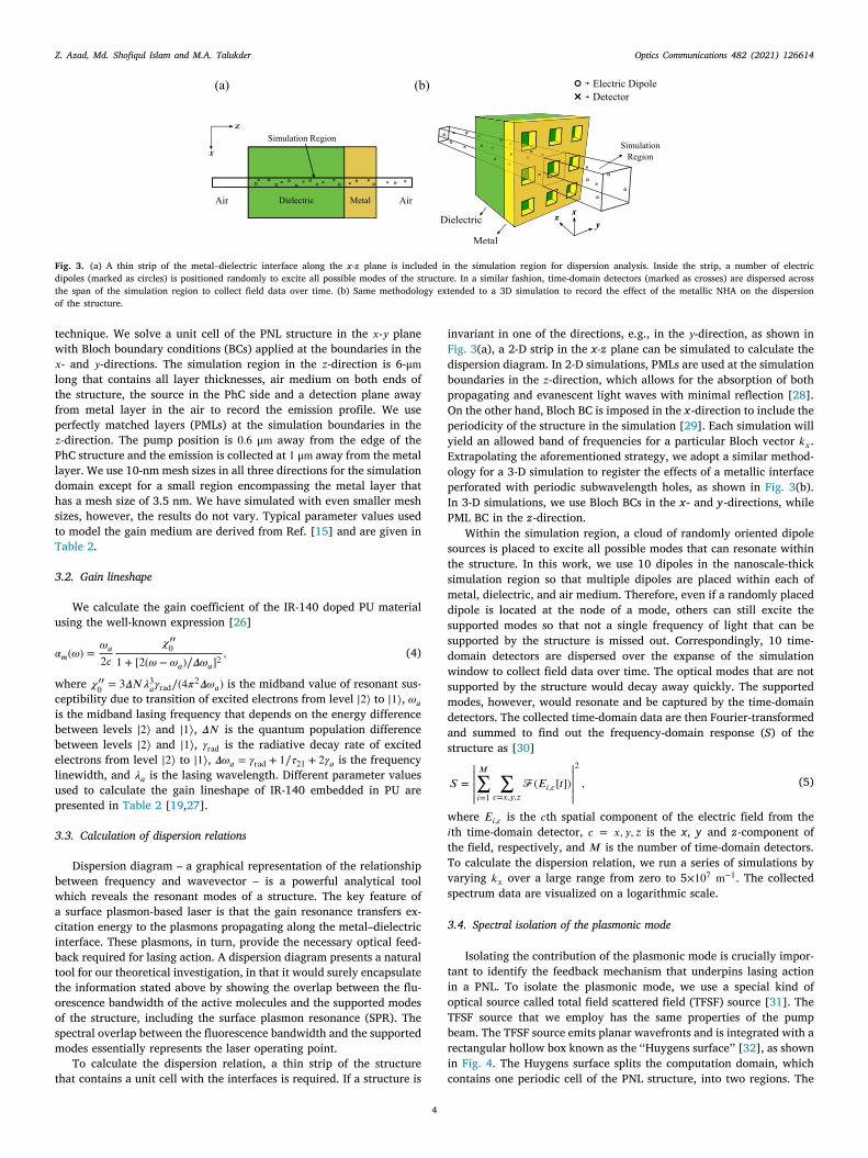
Fig. 3. (a) A thin strip of the metal–dielectric interface along the x-z plane is included in the simulation region for dispersion analysis. Inside the strip, a number of electricipoles (marked as circles) is positioned randomly to excite all possible modes of the structure. In a similar fashion, time-domain detectors (marked as crosses) are dispersed acrosshe span of the simulation region to collect field data over time. (b) Same methodology extended to a 3D simulation to record the effect of the metallic NHA on the dispersionf the structure.
pO
s
echnique. We solve a unit cell of the PNL structure in the 𝑥-𝑦 planeith Bloch boundary conditions (BCs) applied at the boundaries in the- and 𝑦-directions. The simulation region in the 𝑧-direction is 6-μmong that contains all layer thicknesses, air medium on both ends ofhe structure, the source in the PhC side and a detection plane awayrom metal layer in the air to record the emission profile. We useerfectly matched layers (PMLs) at the simulation boundaries in the-direction. The pump position is 0.6 μm away from the edge of thehC structure and the emission is collected at 1 μm away from the metalayer. We use 10-nm mesh sizes in all three directions for the simulationomain except for a small region encompassing the metal layer thatas a mesh size of 3.5 nm. We have simulated with even smaller meshizes, however, the results do not vary. Typical parameter values usedo model the gain medium are derived from Ref. [15] and are given inable 2.
.2. Gain lineshape
We calculate the gain coefficient of the IR-140 doped PU materialsing the well-known expression [26]
𝑚(𝜔) =𝜔𝑎2𝑐
𝜒 ′′0
1 + [2(𝜔 − 𝜔𝑎)∕𝛥𝜔𝑎]2, (4)
where 𝜒 ′′0 = 3𝛥𝑁𝜆3𝑎𝛾rad∕(4𝜋
2𝛥𝜔𝑎) is the midband value of resonant sus-ceptibility due to transition of excited electrons from level |2⟩ to |1⟩, 𝜔𝑎is the midband lasing frequency that depends on the energy differencebetween levels |2⟩ and |1⟩, 𝛥𝑁 is the quantum population differencebetween levels |2⟩ and |1⟩, 𝛾rad is the radiative decay rate of excitedelectrons from level |2⟩ to |1⟩, 𝛥𝜔𝑎 = 𝛾rad + 1∕𝜏21 + 2𝛾𝑎 is the frequencylinewidth, and 𝜆𝑎 is the lasing wavelength. Different parameter valuessed to calculate the gain lineshape of IR-140 embedded in PU areresented in Table 2 [19,27].
.3. Calculation of dispersion relations
Dispersion diagram – a graphical representation of the relationshipetween frequency and wavevector – is a powerful analytical toolhich reveals the resonant modes of a structure. The key feature ofsurface plasmon-based laser is that the gain resonance transfers ex-
itation energy to the plasmons propagating along the metal–dielectricnterface. These plasmons, in turn, provide the necessary optical feed-ack required for lasing action. A dispersion diagram presents a naturalool for our theoretical investigation, in that it would surely encapsulatehe information stated above by showing the overlap between the flu-rescence bandwidth of the active molecules and the supported modesf the structure, including the surface plasmon resonance (SPR). Thepectral overlap between the fluorescence bandwidth and the supportedodes essentially represents the laser operating point.
To calculate the dispersion relation, a thin strip of the structure
hat contains a unit cell with the interfaces is required. If a structure is4
invariant in one of the directions, e.g., in the 𝑦-direction, as shown inFig. 3(a), a 2-D strip in the x-z plane can be simulated to calculate thedispersion diagram. In 2-D simulations, PMLs are used at the simulationboundaries in the 𝑧-direction, which allows for the absorption of bothropagating and evanescent light waves with minimal reflection [28].n the other hand, Bloch BC is imposed in the x-direction to include the
periodicity of the structure in the simulation [29]. Each simulation willyield an allowed band of frequencies for a particular Bloch vector 𝑘𝑥.Extrapolating the aforementioned strategy, we adopt a similar method-ology for a 3-D simulation to register the effects of a metallic interfaceperforated with periodic subwavelength holes, as shown in Fig. 3(b).In 3-D simulations, we use Bloch BCs in the x- and y-directions, whilePML BC in the z-direction.
Within the simulation region, a cloud of randomly oriented dipolesources is placed to excite all possible modes that can resonate withinthe structure. In this work, we use 10 dipoles in the nanoscale-thicksimulation region so that multiple dipoles are placed within each ofmetal, dielectric, and air medium. Therefore, even if a randomly placeddipole is located at the node of a mode, others can still excite thesupported modes so that not a single frequency of light that can besupported by the structure is missed out. Correspondingly, 10 time-domain detectors are dispersed over the expanse of the simulationwindow to collect field data over time. The optical modes that are notsupported by the structure would decay away quickly. The supportedmodes, however, would resonate and be captured by the time-domaindetectors. The collected time-domain data are then Fourier-transformedand summed to find out the frequency-domain response (S) of thetructure as [30]
𝑆 =|
|
|
|
|
|
𝑀∑
𝑖=1
∑
𝑐=𝑥,𝑦,𝑧ℱ (𝐸𝑖,𝑐 [𝑡])
|
|
|
|
|
|
2
, (5)
where 𝐸𝑖,𝑐 is the 𝑐th spatial component of the electric field from the𝑖th time-domain detector, 𝑐 = 𝑥, 𝑦, 𝑧 is the x, y and z-component ofthe field, respectively, and 𝑀 is the number of time-domain detectors.To calculate the dispersion relation, we run a series of simulations byvarying 𝑘𝑥 over a large range from zero to 5×10⁷ m−1. The collectedspectrum data are visualized on a logarithmic scale.
3.4. Spectral isolation of the plasmonic mode
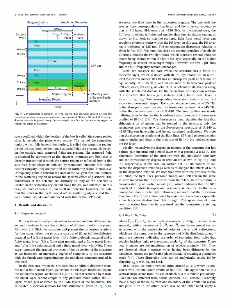
Isolating the contribution of the plasmonic mode is crucially impor-tant to identify the feedback mechanism that underpins lasing actionin a PNL. To isolate the plasmonic mode, we use a special kind ofoptical source called total field scattered field (TFSF) source [31]. TheTFSF source that we employ has the same properties of the pumpbeam. The TFSF source emits planar wavefronts and is integrated with arectangular hollow box known as the ‘‘Huygens surface’’ [32], as shownin Fig. 4. The Huygens surface splits the computation domain, whichcontains one periodic cell of the PNL structure, into two regions. The
Z. Azad, Md. Shofiqul Islam and M.A. Talukder Optics Communications 482 (2021) 126614
s
tc
4
4
ePfmfacawt
rttlc
Fig. 4. 2-D schematic illustration of TFSF source. The Huygens surface divides theimulation window into source and scattering regions. A 50 nm × 50 nm 2-D frequency
domain detector is placed along the metal–gain interface in the scattering region torecord the effect of plasmons.
space confined within the borders of the box is called the source regionsince it includes the plane wave source. The rest of the simulationregion, which falls beyond the borders, is called the scattering region.Inside the box, both incident and scattered fields are present. However,on the outside, only scattered fields are present. The scattered fieldis obtained by subtracting at the Huygens interfaces any light that isdirectly transmitted through the source region or reflected from a flatsubstrate. Since plasmons induced by stimulated emission falls underneither category, they are plentiful in the scattering region. Hence, a 2-D frequency-domain detector is placed at the Au–gain medium interfacein the scattering region to record the spectral effect of plasmons. Thedimensions of the detector are arbitrary so long as the detector islocated in the scattering region and along the Au–gain interface. In thiscase, we have chosen a 50 nm × 50 nm detector. However, we notehat the holes in the metal would act as scattering objects, and theirontribution would come interlaced with that of the SPP mode.
. Results and discussion
.1. Dispersion analysis
For a systematic analysis, as well as to understand how different lay-rs and interfaces impact the excitation of different modes in a planarNL with 2-D NHA, we calculate and present the dispersion relationsor four cases: When the structure consists of (i) an infinite dielectricaterial and a finite metal layer, (ii) a finite dielectric material and a
inite metal layer, (iii) a finite gain material and a finite metal layer,nd (iv) a finite gain material and a finite metal layer with NHA. Theseases represent the gradual evolution of the dispersion of the structures we introduce an increasing degree of complexity to the structureith the fourth case approximating the nanolaser structure studied in
his work.In the first case, when the structure has an infinite dielectric mate-
ial and a finite metal layer, we extend the PU layer thickness beyondhe simulation region, as shown in Fig. 5(a), so that scattered light fromhe metal layer cannot couple to any photonic mode within the PUayer, rather gets absorbed by the PML layers at the boundary. Thealculated dispersion relation for this structure is given in Fig. 5(b).
5
We note two light lines in the dispersion diagram: The one with thegreater slope corresponds to that in air and the other corresponds tothat in PU layer. SPR occurs at ∼550 THz. In the second case, thePU layer thickness is finite and smaller than the simulation region, asshown in Fig. 5(c), so that the scattered light from metal layer cancouple to photonic modes within the PU layer. In this case, the PU layerhas a thickness of 325 nm. The corresponding dispersion relation isgiven in Fig. 5(d). We note that there are several branches of availablesolutions between the two light lines, which represent several photonicmodes being excited within the finite PU layer, especially, in the higherfrequency or shorter wavelength range. However, the two light linesand the SPR frequency remain unchanged.
Now, we consider the case when the structure has a finite PUdielectric layer, which is doped with IR-140 dye molecules. In our 4-level 2-electron model, IR-140 has an absorption peak at 800 nm, orequivalently, at ∼375 THz, and an emission or fluorescence peak at870 nm, or equivalently, at ∼345 THz. A schematic illustration alongwith the simulation domain for the calculation of dispersion relationof a structure that has a gain material and a finite metal layer isshown in Fig. 5(e). The corresponding dispersion relation in Fig. 5(f)shows two horizontal stripes: The upper stripe centered at ∼375 THzis the absorption spectrum and the lower one centered at ∼345 THzis the fluorescence spectrum of IR-140. The two profiles are nearlyindistinguishable due to the broadband absorption and fluorescenceprofiles of IR-140 [19]. The fluorescence band signifies the fact thatalthough a lot of modes can be excited in the structure, only theresonances that overlap with the fluorescence spectrum of IR-140 at∼345 THz can have gain, and hence, sustained oscillations. We notethat the dispersion relations of the light lines, SPR, and photonic modesremain unchanged despite the inclusion of IR-140 dye molecules intothe PU layer.
Finally, we analyze the dispersion relation of the structure that hasa finite gain material and a metal layer with a periodic 2-D NHA. Theschematic illustration of the structure with the simulation boundaryand the corresponding dispersion relation are shown in Fig. 5(g) and(h), respectively. In this case, we carried out 3-D simulations to cal-culate the dispersion relation as well as to analyze the effects of NHAon the dispersion relation. We note that even with the presence of the2-D NHA, the light lines, photonic modes, and SPR remain the sameas were found for the third case without the 2-D NHA. This finding iscorroborated by an earlier report [33], which indicates that the SPRbranch of a hybrid hole-plasmon resonance is identical to that of apurely continuous metal layer. However, we note that the dispersiondiagram in Fig. 5(h) is criss-crossed by a number of new lines, especiallya few branches slanting from left to right. The appearance of thesenew dispersion lines can be explained via the momentum matchingcondition [34]
𝑘𝑥 ± 𝑖𝐺𝑥 ± 𝑗 𝐺𝑦 = 𝑘sp (6)
where 𝑘𝑥 = 𝑘0 sin 𝜃inc is the in-plane wavevector of light incident at anangle 𝜃inc with a wavevector 𝑘0, 𝐺𝑥 and 𝐺𝑦 are the reciprocal vectorsassociated with the periodicity of holes in the x- and y-directions,which are the same due to the symmetry of NHA distribution, and 𝑖and 𝑗 are integers indicating the order of scattering from holes thatcouples incident light to a resonant mode 𝑘sp of the structure. Thesenew branches are the manifestation of Wood’s anomaly [35]. Theyare observed when a surface wave, having been diffracted by thenanoholes, grazes the perforated plane instead of creating a plasmonicmode [34]. These dispersion lines can be analytically solved for byplugging 𝑘sp = 0 in Eq. (6) [36].
In all cases, we note a vertical stripe around 𝑘𝑥 ≈ 0, which is con-sistent with the simulation results of Ref. [35]. The appearance of thisvertical stripe stems from the use of Bloch BCs to simulate periodicity.Bloch BCs are different from normal periodic BCs. Periodic BCs simplymake a copy of the fields from one boundary of the simulation region
and paste it on to the other. Bloch BCs, on the other hand, apply a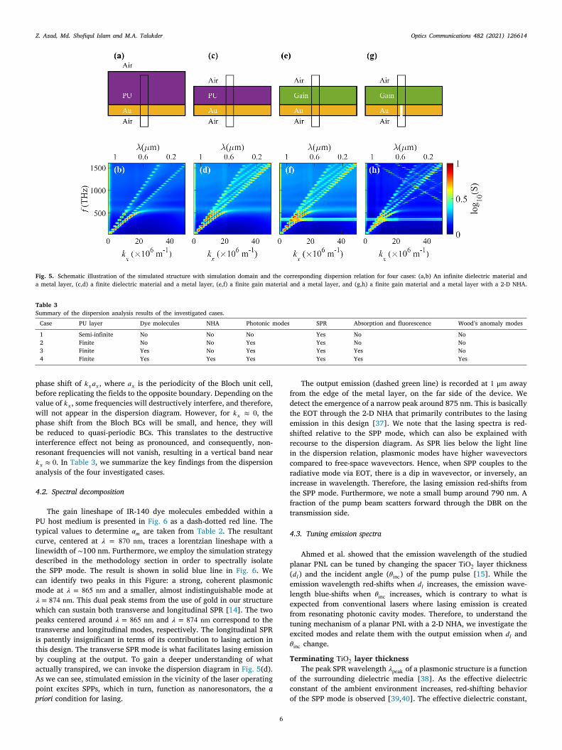
Z. Azad, Md. Shofiqul Islam and M.A. Talukder Optics Communications 482 (2021) 126614
Fig. 5. Schematic illustration of the simulated structure with simulation domain and the corresponding dispersion relation for four cases: (a,b) An infinite dielectric material anda metal layer, (c,d) a finite dielectric material and a metal layer, (e,f) a finite gain material and a metal layer, and (g,h) a finite gain material and a metal layer with a 2-D NHA.
Table 3Summary of the dispersion analysis results of the investigated cases.
Case PU layer Dye molecules NHA Photonic modes SPR Absorption and fluorescence Wood’s anomaly modes
1 Semi-infinite No No No Yes No No2 Finite No No Yes Yes No No3 Finite Yes No Yes Yes Yes No4 Finite Yes Yes Yes Yes Yes Yes
fdtesricritft
4
p(
phase shift of 𝑘𝑥𝑎𝑥, where 𝑎𝑥 is the periodicity of the Bloch unit cell,before replicating the fields to the opposite boundary. Depending on thevalue of 𝑘𝑥, some frequencies will destructively interfere, and therefore,will not appear in the dispersion diagram. However, for 𝑘𝑥 ≈ 0, thephase shift from the Bloch BCs will be small, and hence, they willbe reduced to quasi-periodic BCs. This translates to the destructiveinterference effect not being as pronounced, and consequently, non-resonant frequencies will not vanish, resulting in a vertical band near𝑘𝑥 ≈ 0. In Table 3, we summarize the key findings from the dispersionanalysis of the four investigated cases.
4.2. Spectral decomposition
The gain lineshape of IR-140 dye molecules embedded within aPU host medium is presented in Fig. 6 as a dash-dotted red line. Thetypical values to determine 𝛼𝑚 are taken from Table 2. The resultantcurve, centered at 𝜆 = 870 nm, traces a lorentzian lineshape with alinewidth of ∼100 nm. Furthermore, we employ the simulation strategydescribed in the methodology section in order to spectrally isolatethe SPP mode. The result is shown in solid blue line in Fig. 6. Wecan identify two peaks in this Figure: a strong, coherent plasmonicmode at 𝜆 = 865 nm and a smaller, almost indistinguishable mode at𝜆 = 874 nm. This dual peak stems from the use of gold in our structurewhich can sustain both transverse and longitudinal SPR [14]. The twopeaks centered around 𝜆 = 865 nm and 𝜆 = 874 nm correspond to thetransverse and longitudinal modes, respectively. The longitudinal SPRis patently insignificant in terms of its contribution to lasing action inthis design. The transverse SPR mode is what facilitates lasing emissionby coupling at the output. To gain a deeper understanding of whatactually transpired, we can invoke the dispersion diagram in Fig. 5(d).As we can see, stimulated emission in the vicinity of the laser operatingpoint excites SPPs, which in turn, function as nanoresonators, the apriori condition for lasing.
6
The output emission (dashed green line) is recorded at 1 μm awayrom the edge of the metal layer, on the far side of the device. Weetect the emergence of a narrow peak around 875 nm. This is basicallyhe EOT through the 2-D NHA that primarily contributes to the lasingmission in this design [37]. We note that the lasing spectra is red-hifted relative to the SPP mode, which can also be explained withecourse to the dispersion diagram. As SPR lies below the light linen the dispersion relation, plasmonic modes have higher wavevectorsompared to free-space wavevectors. Hence, when SPP couples to theadiative mode via EOT, there is a dip in wavevector, or inversely, anncrease in wavelength. Therefore, the lasing emission red-shifts fromhe SPP mode. Furthermore, we note a small bump around 790 nm. Araction of the pump beam scatters forward through the DBR on theransmission side.
.3. Tuning emission spectra
Ahmed et al. showed that the emission wavelength of the studiedlanar PNL can be tuned by changing the spacer TiO2 layer thickness𝑑𝑙) and the incident angle (𝜃inc) of the pump pulse [15]. While the
emission wavelength red-shifts when 𝑑𝑙 increases, the emission wave-length blue-shifts when 𝜃inc increases, which is contrary to what isexpected from conventional lasers where lasing emission is createdfrom resonating photonic cavity modes. Therefore, to understand thetuning mechanism of a planar PNL with a 2-D NHA, we investigate theexcited modes and relate them with the output emission when 𝑑𝑙 and𝜃inc change.
Terminating TiO2 layer thicknessThe peak SPR wavelength 𝜆peak of a plasmonic structure is a function
of the surrounding dielectric media [38]. As the effective dielectricconstant of the ambient environment increases, red-shifting behaviorof the SPP mode is observed [39,40]. The effective dielectric constant,
Z. Azad, Md. Shofiqul Islam and M.A. Talukder Optics Communications 482 (2021) 126614
l
iTnTlso
liC9
Fig. 6. The gain lineshape of IR-140 and the confined and emitted modal componentsof the studied PNL. The surface plasmon mode has been calculated at the metal-DBRinterface and the radiative mode has been calculated at 1 μm away from the edge ofthe metal layer.
Fig. 7. The peak positions (𝜆peak ) of output emission and SPP modes as (a) spacer TiO2ayer thickness (𝑑𝑙) increases and (b) incident angle (𝜃inc) increases.
n turn, is positively correlated with the thickness of the dielectric layer:he thicker the layer, the greater the dielectric constant. This phe-omenon can be explained with recourse to the local field theory [41].herefore, theoretically speaking, if the thickness of the spacer TiO2
ayer increases, the SPP mode should red-shift and the lasing modehould follow suit, given that the lasing emission principally dependsn the plasmonic mode.
This is exactly the pattern that emerges in Fig. 7(a) as the spacerayer thickness 𝑑𝑙 increases. We find that 𝜆peak for the SPP modencreases from 824 nm to 921 nm, as 𝑑𝑙 varies from 145 nm to 255 nm.orrespondingly, 𝜆peak for the lasing emission changes from 840 nm to28 nm. However, the tunability range of 𝜆peak for the lasing emission
is capped on both ends. No lasing is observed beyond either 𝑑𝑙 ≲ 140 nmor 𝑑𝑙 ≳ 260 nm. The change of location of 𝜆peak of the SPP modewith respect to the gain lineshape explains the vanishing of the lasingemission. As 𝑑𝑙 varies, the SPP mode eventually shifts away from thegain linewidth of IR-140 in both directions, which is shown by thedashed green line in Fig. 7(a). Hence, the gain medium can no longercompensate for the intrinsic loss of the PNL system and lasing emissionceases.
Incidence angle of the pump pulseThe resonant wavelength of plasmonic modes also changes when
the incident angle of the pump pulse varies [16,42,43]. Zhou et al.demonstrated in their nanocavity array-based plasmonic laser thatemission spectra blue-shifts from 913 nm to 850 nm when the incidenceangle increases from 0 to 40◦ [44]. We explore the physics of theincidence angle-dependent tunability mechanism of the planar PNL
design studied in this work.7
We note that 𝜆peak of both the lasing emission and the SPP modeblue-shifts with the increase of 𝜃inc, as shown in Fig. 7(b). The 𝜆peak ofSPP decreases from 866 nm to 831 nm as the incidence angle variesfrom 0 to 35◦. Likewise, the lasing mode blue-shifts from 879 nmto 858 nm. Similar to the previous case, there is an upper limit fortunability. No lasing is observed beyond the critical angle 𝜃inc = 35◦
since the SPP mode strays too far from the peak of the gain emissionof IR-140 dye molecules. The reason behind the blue-shifting of lasingemission can be qualitatively understood from the dispersion diagrams.As 𝜃inc increases, plasmonic resonance moves to a larger wavevector 𝑘sp,as can be seen from Eq. (6). With increasing 𝑘sp, plasmonic mode shiftsto a lower 𝜆peak , and consequently, the lasing emission blueshifts too.We also note that the tunable range with the change in 𝜃inc is smallerthan that obtained with the change in 𝑑𝑙.
We find that the SPP mode trails the lasing mode and always movesin lockstep with the lasing mode. A red- or blue-shift of the SPP modeproduces a similar behavior for the lasing mode. This vital informationpresents us with a scientific strategy to tune the emission spectra ofa PNL. Via this route, the emission spectra of PNLs can be tunedproactively over a broad range.
5. Conclusion
In this work, we identified the constitutive elements of a plasmon-mediated nanolaser. We isolated the SPP mode that emerges at themetal–dielectric interface and found that the SPP mode is definitivelylinked with the lasing emission in a planar PNL with 2-D metallic NHA.The calculated dispersion relations explain the excitation of SPP modesin the parallel plane PNL structure and the coupling between free-spaceand surface-bound modes. Our detailed analysis showed that the SPPmode is the critical determinant of lasing action of a planar PNL, whichcan be used as a tool to tune the emission spectra as well. Although thiswork deals with a planar PNL, similar behavior will evolve in nanowire-and nanoparticle-based PNL designs as plasmonic modes will play amore significant role in those designs.
Declaration of competing interest
The authors declare that they have no known competing finan-cial interests or personal relationships that could have appeared toinfluence the work reported in this paper.
Funding
This research did not receive any specific grant from funding agen-cies in the public, commercial, or not-for-profit sectors.
References
[1] Ren-Min Ma, Rupert F. Oulton, Applications of nanolasers, Nature Nanotechnol.14 (1) (2019) 12–22.
[2] Cun-Zheng Ning, Semiconductor nanolasers and the size-energy-efficiencychallenge: a review, Adv. Photonics 1 (1) (2019) 014002.
[3] Chun Li, Zhen Liu, Jie Chen, Yan Gao, Meili Li, Qing Zhang, Semiconductornanowire plasmonic lasers, Nanophotonics 8 (12) (2019) 2091–2110.
[4] Litu Xu, Fang Li, Yahui Liu, Fuqiang Yao, Shuai Liu, Surface plasmon nanolaser:Principle, structure, characteristics and applications, Appl. Sci. 9 (5) (2019) 861.
[5] Shaimaa I. Azzam, Alexander V. Kildishev, Ren-Min Ma, Cun-Zheng Ning, RupertOulton, Vladimir M. Shalaev, Mark I. Stockman, Jia-Lu Xu, Xiang Zhang, Tenyears of spasers and plasmonic nanolasers, Light: Sci. Appl. 9 (1) (2020) 1–21.
[6] Stefan Alexander Maier, Plasmonics: Fundamentals and Applications, SpringerScience & Business Media, 2007.
[7] Martin T. Hill, Yok-Siang Oei, Barry Smalbrugge, Youcai Zhu, Tjibbe De Vries,Peter J. Van Veldhoven, Frank W.M. Van Otten, Tom J. Eijkemans, Jaroslaw P.Turkiewicz, Huug De Waardt, et al., Lasing in metallic-coated nanocavities,Nature Photonics 1 (10) (2007) 589.
[8] Shao-Lei Wang, Suo Wang, Xing-Kun Man, Ren-Min Ma, Loss and gain in aplasmonic nanolaser, Nanophotonics 1 (ahead-of-print) (2020).
[9] Rupert F. Oulton, Volker J. Sorger, Thomas Zentgraf, Ren-Min Ma, Christo-pher Gladden, Lun Dai, Guy Bartal, Xiang Zhang, Plasmon lasers at deepsubwavelength scale, Nature 461 (7264) (2009) 629.
Z. Azad, Md. Shofiqul Islam and M.A. Talukder Optics Communications 482 (2021) 126614
[10] Kuankuan Ren, Jian Wang, Shaoqiang Chen, Qingxin Yang, Jiao Tian, HaichaoYu, Mingfei Sun, Xiaojun Zhu, Shizhong Yue, Yang Sun, et al., Realization ofperovskite-nanowire-based plasmonic lasers capable of mode modulation, LaserPhotonics Rev. 13 (7) (2019) 1800306.
[11] R.F. Oulton, G. Bartal, D.F.P. Pile, Xiang Zhang, Confinement and propagationcharacteristics of subwavelength plasmonic modes, New J. Phys. 10 (10) (2008)105018.
[12] Chi Pang, Rang Li, Ziqi Li, Ningning Dong, Jun Wang, Feng Ren, Feng Chen,Plasmonic Ag nanoparticles embedded in lithium tantalate crystal for ultrafastlaser generation, Nanotechnology 30 (33) (2019) 334001.
[13] Jie Yang, Zhengzheng Liu, Zhiping Hu, Fanju Zeng, Zeyu Zhang, Yao Yao,Zhiqiang Yao, Xiaosheng Tang, Juan Du, Zhigang Zang, et al., Enhanced single-mode lasers of all-inorganic perovskite nanocube by localized surface plasmoniceffect from Au nanoparticles, J. Lumin. 208 (2019) 402–407.
[14] Xiangeng Meng, Alexander V. Kildishev, Koji Fujita, Katsuhisa Tanaka,Vladimir M. Shalaev, Wavelength-tunable spasing in the visible, Nano Lett. 13(9) (2013) 4106–4112.
[15] Zabir Ahmed, Muhammad Anisuzzaman Talukder, An efficient and directionaloptical tamm state assisted plasmonic nanolaser with broad tuning range, J.Phys. Commun. 2 (4) (2018) 045016.
[16] M. Kaliteevski, I. Iorsh, S. Brand, R.A. Abram, J.M. Chamberlain, A.V. Kavokin,I.A. Shelykh, Tamm plasmon-polaritons: Possible electromagnetic states at theinterface of a metal and a dielectric Bragg mirror, Phys. Rev. B 76 (16) (2007)165415.
[17] Yang Mi, Bao Jin, Liyun Zhao, Jie Chen, Shuai Zhang, Jia Shi, Yangguang Zhong,Wenna Du, Jun Zhang, Qing Zhang, et al., High-quality hexagonal nonlayeredCdS nanoplatelets for low-threshold whispering-gallery-mode lasing, Small 15(35) (2019) 1901364.
[18] Qing Zhang, Son Tung Ha, Xinfeng Liu, Tze Chien Sum, Qihua Xiong,Room-temperature near-infrared high-Q perovskite whispering-gallery planarnanolasers, Nano Lett. 14 (10) (2014) 5995–6001.
[19] Jyotirmayee Mohanty, Dipakk Palit, J.P. Mittal, Photophysical properties of twoinfrared laser dyes–IR-144 and IR-140: A picosecond laser flash photolysis study,Proc.-Indian Natl. Sci. Acad. A 66 (2) (2000) 303–315.
[20] Maude Amyot-Bourgeois, Elham Karami Keshmarzi, Choloong Hahn, R. NiallTait, Pierre Berini, Gain optimization, bleaching, and e-beam structuring ofIR-140 doped PMMA and integration with plasmonic waveguides, Opt. Mater.Express 7 (11) (2017) 3963–3978.
[21] Babak Dastmalchi, Philippe Tassin, Thomas Koschny, Costas M. Soukoulis, Anew perspective on plasmonics: confinement and propagation length of surfaceplasmons for different materials and geometries, Adv. Opt. Mater. 4 (1) (2016)177–184.
[22] Aleksandr S. Baburin, Aleksey S. Kalmykov, Roman V. Kirtaev, Dmitriy V.Negrov, Dmitriy O. Moskalev, Ilya A. Ryzhikov, Pavel N. Melentiev, Ilya A.Rodionov, Victor I. Balykin, Toward a theoretically limited SPP propagationlength above two hundred microns on an ultra-smooth silver surface, Opt. Mater.Express 8 (11) (2018) 3254–3261.
[23] Wei Ma, Zhaocheng Liu, Zhaxylyk A Kudyshev, Alexandra Boltasseva, WenshanCai, Yongmin Liu, Deep learning for the design of photonic structures, NaturePhotonics (2020) 1–14.
[24] L.G. Nair, Dye lasers, Prog. Quantum Electron. 7 (3–4) (1982) 153–268.[25] Shih-Hui Chang, Allen Taflove, Finite-difference time-domain model of lasing
action in a four-level two-electron atomic system, Opt. Express 12 (16) (2004)3827–3833.
[26] Anthony E. Siegman, A.E. Siegman, Lasers, Vol. 122, McGraw-Hill, New York,1986, pp. 270–272.
8
[27] Carl M. Liebig, W.M. Dennis, Optical dephasing in saturable-absorbing organicdye IR140, Appl. Opt. 45 (9) (2006) 2072–2076.
[28] Jean-Pierre Bérenger, Perfectly matched layer (PML) for computationalelectromagnetics, Synth. Lect. Comput. Electromagn. 2 (1) (2007) 1–117.
[29] N. Sukumar, J.E. Pask, Classical and enriched finite element formulations forBloch-periodic boundary conditions, Internat. J. Numer. Methods Engrg. 77 (8)(2009) 1121–1138.
[30] H. Sami Sözüer, Joseph W. Haus, Photonic bands: simple-cubic lattice, J. Opt.Soc. Amer. B 10 (2) (1993) 296–302.
[31] Glenn S. Smith, et al., A total-field/scattered-field plane-wave source for theFDTD analysis of layered media, IEEE Trans. Antennas and Propagation 56 (1)(2008) 158–169.
[32] Mike Potter, Jean-Pierre Bérenger, A review of the total field/scattered fieldtechnique for the FDTD method, FERMAT 19 (2017) 1–13.
[33] Tae-Ho Park, Joong-Wook Lee, Daniel M. Mittleman, Peter Nordlander, Polar-ization dependent terahertz spectroscopy of a single subwavelength hole in thinmetallic film, in: Plasmonics: Metallic Nanostructures and their Optical PropertiesVII, Vol. 7394, International Society for Optics and Photonics, 2009, p. 73940F.
[34] H.F. Ghaemi, Tineke Thio, Deeal Grupp, Thomas W. Ebbesen, H.J. Lezec, Surfaceplasmons enhance optical transmission through subwavelength holes, Phys. Rev.B 58 (11) (1998) 6779.
[35] William L. Barnes, W. Andrew Murray, J. Dintinger, E. Devaux, T.W. Ebbesen,Surface plasmon polaritons and their role in the enhanced transmission of lightthrough periodic arrays of subwavelength holes in a metal film, Phys. Rev. Lett.92 (10) (2004) 107401.
[36] Mikhail M. Voronov, Resonant wood’s anomaly diffraction condition in dielectricand plasmonic grating structures, 2016, arXiv preprint arXiv:1612.08674.
[37] K.L. Van der Molen, K.J. Klein Koerkamp, Stefan Enoch, Franciscus B. Segerink,N.F. Van Hulst, L. Kuipers, Role of shape and localized resonances in extraordi-nary transmission through periodic arrays of subwavelength holes: Experimentand theory, Phys. Rev. B 72 (4) (2005) 045421.
[38] G. Xu, M. Tazawa, P. Jin, S. Nakao, K. Yoshimura, Wavelength tuning of surfaceplasmon resonance using dielectric layers on silver island films, Appl. Phys. Lett.82 (22) (2003) 3811–3813.
[39] G. Xu, M. Tazawa, P. Jin, S. Nakao, Surface plasmon resonance of sputtered agfilms: substrate and mass thickness dependence, Appl. Phys. A 80 (7) (2005)1535–1540.
[40] Gang Xu, Chun-Ming Huang, Qing Liang, Masato Tazawa, Ping Jin, Wavelengthmultiplexing and tuning in nano-ag/dielectric multilayers, Appl. Phys. A 94 (3)(2009) 525–530.
[41] Kenji Natori, Daijiro Otani, Nobuyuki Sano, Thickness dependence of theeffective dielectric constant in a thin film capacitor, Appl. Phys. Lett. 73 (5)(1998) 632–634.
[42] Ying-Shin Huang, Sheng-Yao Hu, Chia-Chih Huang, Yueh-Chien Lee, Jyh-Wei Lee,Chung-Cheng Chang, Zin-Kuan Wun, Kwong-Kau Tiong, Incident-angle-dependentreflectance in distributed bragg reflectors fabricated from ZnO/MgO multilayerfilms, Opt. Rev. 21 (5) (2014) 651–654.
[43] A.V. Kavokin, I.A. Shelykh, G. Malpuech, Lossless interface modes at theboundary between two periodic dielectric structures, Phys. Rev. B 72 (23) (2005)233102.
[44] Wei Zhou, Montacer Dridi, Jae Yong Suh, Chul Hoon Kim, Dick T. Co, Michael R.Wasielewski, George C. Schatz, Teri W. Odom, et al., Lasing action in stronglycoupled plasmonic nanocavity arrays, Nature Nanotechnol. 8 (7) (2013) 506.


![Enhancing the Angular Sensitivity of Plasmonic Sensors ...biotheory.phys.cwru.edu/PDF/AOM.pdf · ultrasensitive plasmonic biosensors.[29,30] A plasmonic nanorod metamaterial (Type](https://img.pdfslide.us/doc/110x75/5fcdd2c6db367d06a677e7be/enhancing-the-angular-sensitivity-of-plasmonic-sensors-ultrasensitive-plasmonic.jpg)


![Nano and Photonics Mauterndorf 2019 · transistor [2]. In electro plasmonics we demonstrate pretty efficient light generation in a planar plasmonic antenna by utilizing inelastic](https://img.pdfslide.us/doc/110x75/5f0859387e708231d421910a/nano-and-photonics-mauterndorf-transistor-2-in-electro-plasmonics-we-demonstrate.jpg)