Embed Size (px)
Citation preview
Nanoconcentration of terahertzradiation in plasmonic waveguides
Anastasia Rusina1, Maxim Durach1, Keith A. Nelson2, and Mark I.Stockman1,3,∗
1Department of Physics and Astronomy, Georgia State University, Atlanta, Georgia 30303,USA
2Department of Chemistry, MIT, Cambridge, MA 02139, USA
3On sabbatical leave at Ecole Superieure de Physique et de Chimie Industrielle de la Ville deParis, 10, rue Vauquelin, 75231 Paris, CEDEX 05, France
∗http://www.phy-astr.gsu.edu/stockman
Abstract: We establish the principal limits for the nanoconcentrationof the THz radiation in metal/dielectric waveguides and determine theiroptimum shapes required for this nanoconcentration. We predict that theadiabatic compression of THz radiation from the initial spot size of R 0 ∼ λ0
to the final size of R = 100− 250 nm can be achieved, while the THzradiation intensity is increased by a factor of ×10 to ×250. This THzenergy nanoconcentration will not only improve the spatial resolutionand increase the signal/noise ratio for the THz imaging and spectroscopy,but in combination with the recently developed sources of powerful THzpulses will allow the observation of nonlinear THz effects and a variety ofnonlinear spectroscopies (such as two-dimensional spectroscopy), whichare highly informative. This will find a wide spectrum of applications inscience, engineering, biomedical research, environmental monitoring, anddefense.
© 2008 Optical Society of America
OCIS codes: (250.5403) Plasmonics; (300.6495) Spectroscopy, terahertz; (240.6690) Surfacewaves; (230.7370) Waveguides
References and links1. L. Novotny and B. Hecht, Principles of Nano-Optics (Cambridge University Press, Cambridge, New York, 2006).2. M. I. Stockman, “Nanofocusing of optical energy in tapered plasmonic waveguides,” Phys. Rev. Lett. 93,
137404–1–4 (2004).3. E. Verhagen, L. Kuipers, and A. Polman, “Enhanced nonlinear optical effects with a tapered plasmonic
waveguide,” Nano Lett. 7, 334–337 (2007).4. C. Ropers, C. C. Neacsu, T. Elsaesser, M. Albrecht, M. B. Raschke, and C. Lienau, “Grating-coupling of surface
plasmons onto metallic tips: A nano-confined light source,” Nano Lett. 7, 2784–2788 (2007).5. E. Verhagen, A. Polman, and L. Kuipers, “Nanofocusing in laterally tapered plasmonic waveguides,” Opt. Ex-
press 16, 45–57 (2008).6. L. Novotny and S. J. Stranick, “Near-field optical microscopy and spectroscopy with pointed probes,” Annu. Rev.
Phys. Chem. 57, 303–331 (2006).7. A. Lewis, H. Taha, A. Strinkovski, A. Manevitch, A. Khatchatouriants, R. Dekhter, and E. Ammann, “Near-
field optics: From subwavelength illumination to nanometric shadowing,” Nature Biotechnology 21, 1377–1386(2003).
(C) 2008 OSA 10 November 2008 / Vol. 16, No. 23 / OPTICS EXPRESS 18576#101088 - $15.00 USD Received 3 Sep 2008; revised 23 Oct 2008; accepted 24 Oct 2008; published 27 Oct 2008
8. J. Seelig, K. Leslie, A. Renn, S. Kuhn, V. Jacobsen, M. van de Corput, C. Wyman, and V. Sandoghdar,“Nanoparticle-induced fluorescence lifetime modification as nanoscopic ruler: Demonstration at the single mole-cule level,” Nano Lett. 7, 685–689 (2007).
9. F. D. Angelis, M. Patrini, G. Das, I. Maksymov, M. Galli, L. Businaro, L. C. Andreani, and E. D. Fabrizio, “Ahybrid plasmonic-photonic nanodevice for label-free detection of a few molecules,” Nano Lett. 8, 2321-2327(2008).
10. W. L. Chan, J. Deibel, and D. M. Mittleman, “Imaging with terahertz radiation,” Rep. Prog. Phys. 70, 1325–1379(2007).
11. H. T. Chen, R. Kersting, and G. C. Cho, “Terahertz imaging with nanometer resolution,” Appl. Phys. Lett. 83,3009–3011 (2003).
12. N. Klein, P. Lahl, U. Poppe, F. Kadlec, and P. Kuzel, “A netal-dielectric antenna for terahertz near-field imaging,”J. Appl. Phys. 98, 014910–1–5 (2005).
13. F. Keilmann, “Scanning tip for optical radiation,” in U. S. Patent 4,994,818, pp. 1-7 (Max Plank Geselschaft,Germany, USA, 1991).
14. R. Lecaque, S. Gresillon, and C. Boccara, “THz emission microscopy with sub-wavelength broadband source,”Opt. Express 16, 4731–4738 (2008).
15. M. A. Ordal, L. L. Long, R. J. Bell, S. E. Bell, R. R. Bell, J. R. W. Alexander, and C. A. Ward, “Optical propertiesof the metals Al, Co, Cu, Au, Fe, Pb, Ni, Pd, Pt, Ag, Ti, and W in the infrared and far infrared,” Appl. Opt. 22,1099–1119 (1983).
16. A. Sommerfeld, “Ueber die Fortpflanzung elektrodynamischer Wellen laengs eines Drahtes,” Ann. Phys. Chem.67, 233 – 290 (1899).
17. J. Zenneck, “Fortplfanzung ebener elektromagnetischer Wellen laengs einer ebenen Leiterflaeche,” Ann. Phys.23, 846–866 (1907).
18. J. Saxler, J. Gomez Rivas, C. Janke, H. P. M. Pellemans, P. H. Bolivar, and H. Kurz, “Time-domain measurementsof surface plasmon polaritons in the terahertz frequency range,” Phys. Rev. B 69, 155427–1–4 (2004).
19. D. L. Mills and A. A. Maradudin, “Surface corrugation and surface-polariton binding in the infrared frequencyrange,” Phys. Rev. B 39, 1569–1574 (1989).
20. J. B. Pendry, L. Martin-Moreno, and F. J. Garcia-Vidal, “Mimicking surface plasmons with structured surfaces,”Science 305, 847–848 (2004).
21. F. J. Garcia-Vidal, L. Martin-Moreno, and J. B. Pendry, “Surfaces with holes in them: New plasmonic metama-terials,” J. Opt. A 7, S97–S101 (2005).
22. S. A. Maier, S. R. Andrews, L. Martin-Moreno, and F. J. Garcia-Vidal, “Terahertz surface plasmon-polaritonpropagation and focusing on periodically corrugated metal wires,” Phys. Rev. Lett. 97, 176805–1–4 (2006).
23. F. Keilmann, “FIR microscopy,” Infrared Physics and Technology 36, 217–224 (1995).24. A. Kramer, F. Keilmann, B. Knoll, and R. Guckenberger, “The coaxial tip as a nano-antenna for scanning near-
field microwave transmission microscopy,” Micron 27, 413–417 (1996).25. F. Keilmann, D. W. van der Weide, T. Eickelkamp, R. Merz, and D. Stockle, “Extreme sub-wavelength resolution
with a scanning radio-frequency transmission microscope,” Opt. Commun. 129, 15–18 (1996).26. J. Hebling, K. L. Yeh, M. C. Hoffmann, and K. A. Nelson, “High-power THz generation, THz nonlinear optics,
and THz nonlinear spectroscopy,” IEEE J. Sel. Top. Quantum Electron. 14, 345–353 (2008).27. Y. Shen, T. Watanabe, D. A. Arena, C. C. Kao, J. B. Murphy, T. Y. Tsang, X. J. Wang, and G. L. Carr, “Nonlinear
cross-phase modulation with intense single-cycle terahertz pulses,” Phys. Rev. Lett. 99, 043901–1–4 (2007).28. S. Komiyama, O. Astafiev, V. Antonov, T. Kutsuwa, and H. Hirai, “A single-photon detector in the far-infrared
range,” Nature 403, 405–407 (2000).29. B. Ferguson and X.-C. Zhang, “Materials for terahertz science and technology,” Nature Materials 1, 26–33
(2002).30. M. Tonouchi, “Cutting-edge terahertz technology,” Nature Photonics 1, 97–105 (2007).31. D. Dragoman and M. Dragoman, “Terahertz fields and applications,” Prog. Quantum Electron. 28, 1–66 (2004).32. K. V. Nerkararyan, A. A. Hakhoumian, and A. E. Babayan, “Terahertz surface plasmon-polariton superfocusing
in coaxial cone semiconductor structures,” Plasmonics 3, 27–31 (2008).33. F. Keilmann, “Status of THz-to-visible nanospectroscopy development,” J. Biol. Phys. 29, 195–199 (2003).34. R. Merlin, “Radiationless electromagnetic interference: evanescent-field lenses and perfect focusing,” Science
317, 927–929 (2007).
1. Introduction
Recent years have seen an explosive research and development of nanoplasmonics in the vis-ible and near-infrared (near-ir) frequency regions [1]. One of the most fundamental effectsin nanoplasmonics is nano-concentration of optical energy. Plasmonic nanofocusing has beenpredicted [2] and experimentally achieved [3, 4, 5]. Nanoconcentration of optical energy at
(C) 2008 OSA 10 November 2008 / Vol. 16, No. 23 / OPTICS EXPRESS 18577#101088 - $15.00 USD Received 3 Sep 2008; revised 23 Oct 2008; accepted 24 Oct 2008; published 27 Oct 2008
nanoplasmonic probes made possible optical ultramicroscopy with nanometer-scale resolution[6, 7, 8] and ultrasensitive Raman spectroscopy [9]. It will be very beneficial for the fundamen-tal science, engineering, environmental, and defense applications to be able to nano-concentrateterahertz radiation (frequency 1− 10 THz or vacuum wavelength λ 0 = 300− 30 μm). Thiswill allow for the nanoscale spatial resolution for THz imaging [10] and introduce the THzspectroscopy on the nanoscale, taking full advantage of the rich THz spectra and submicronto nanoscale structures of many engineering, physical, and biological objects of wide inter-est: electronic components (integrated circuits, etc.), bacteria, their spores, viruses, macro-molecules, carbon clusters and nanotubes, etc. There are existing approaches to deep sub-wavelength THz imaging and probing based on sharp tips irradiated by a THz source [11],adiabatically-tapered metal-dielectric waveguides [12] similar to optical adiabatic concentra-tors [13, 2, 3, 4, 5], and nonlinear microscopic THz sources [14]. For the development of theTHz nanotechnology, it is extremely important to understand spatial limits to which the THzradiation energy can be concentrated (nanofocused).
A major challenge for the nanoconcentration of the electromagnetic energy in the THz regionis the large radiation wavelength in vacuum or conventional dielectrics, λ 0 = 30 μm−300 μm,where the THz radiation can only be focused to the relatively very large regions of size ∼λ0/2. The developed field of optical energy concentration, which is based on surface plasmonpolaritons (SPPs), suggests that one of the ways to solving this problem is to employ the surfaceelectromagnetic waves (SEWs). In the far infrared (ir), the dielectric permittivity of metalshas large imaginary part which dominates over its negative real part [15]. This implies thatSEWs propagating along a metal-dielectric flat interface in this frequency range, known asSommerfeld-Zenneck waves [16, 17], are weakly bound to the surface [18] and can hardly beused for the confinement of THz radiation.
It has been suggested that periodically perforating flat surfaces of ideal metals with groovesor holes leads to the appearance of SEWs, which mimic (“spoof”) SPPs to be stronger boundto the surfaces [19, 20, 21] permitting a better control over the THz fields. It has been predictedthat SPPs on an array of parallel grooves cut on the surface of a perfect conductor wire can belocalized by adiabatic deepening of the grooves [22]. At a point, where grooves are approxi-mately a quarter of wavelength of light, the highest concentration is achieved to be on the orderof tens of micrometers. This method restricts the localization point to a particular frequency,making the concentration very narrow-band. Also, the depth of a groove should be ≈ λ 0/4, i.e.,in the tens to hundred micron range, which precludes completely nanoscale devices.
It is well known from microwave technology that the ideal-metal waveguides with smoothsurfaces support TEM waves, where the electric field lines are either infinitely extended orterminate at the metal surfaces normally to them. The latter case requires the waveguide cross-section topology to be more than single-connected; an example may be a coaxial waveguide(“coax”). Such waveguides are very wide-band in frequency. The THz waveguides can be adia-batically tapered to concentrate energy. The idea of adiabatic energy concentration comes fromultramicroscopy [13, 23, 24, 25] and nanoplasmonics [2], where it has been developed boththeoretically and experimentally [3, 4, 5] and used in ultrasensitive surface enhanced Ramanspectroscopy [9]. Employing these ideas of the adiabatic concentration and using a taperedmetal-dielectric waveguide, the THz spatial resolution achieved is ∼ 20 μm across the entireTHz spectrum [12].
In this paper, we establish the fundamental limits and find the principles of designing theoptimum and efficient metal/dielectric nanowaveguides suitable for the THz nanofocusing. Thespecific examples are for the wide-band concentrators: a plasmonic metal wedge cavity andtapered coax waveguides, which are terminated by funnel-type adiabatic tapers. Such nano-concentrators along with the advent of high-power sources [26, 27] and sensitive detectors
(C) 2008 OSA 10 November 2008 / Vol. 16, No. 23 / OPTICS EXPRESS 18578#101088 - $15.00 USD Received 3 Sep 2008; revised 23 Oct 2008; accepted 24 Oct 2008; published 27 Oct 2008
[28] of THz radiation, will open up an extremely wide range of possible THz applications,in particular, in material diagnostics, probe nanoimaging, biomedical applications etc. – cf.[29, 30, 31].
Note that an alternative approach to the THz energy concentration using doped semiconduc-tor tapers has also been proposed [32]. However, the required heavy doping of the semiconduc-tors may cause fast electron relaxation due to the collisions with the inflicted lattice defects andbring about high losses. Therefore, here we will pursue the adiabatic nanoconcentration of theTHz radiation using metal/dielectric structures.
Conventionally for THz and microwave regions, the metals are considered as ideal whichis equivalent to neglecting their skin depth l s = λ 0/Re
√−εm, where εm is the permittivity ofthe metal (we take into accoint that in the THz region |εm| � 1), and λ 0 = c/ω is the reducedwavelength in vacuum. It is true that in the THz region l s = 30−60 nm. i.e., ls � λ0. However,as we show below, it is the finite skin depth, though as small as it is, that principally limitsthe ultimum localization size of the THz fields. For larger waveguides, the THz wave energy islocalized mostly in the vacuum (dielectric) and its losses, which occur in the metal’s skin layer,are correspondingly small. The effective quality factor (or, figure of merit) of the waveguide,which shows how many periods the wave can propagate without significantly loosing its energy,can be estimated as
Q ∼ 2a/ls , (1)
where a is the characteristic minimum size of the waveguide; this estimate becomes a goodapproximation for a metal-dielectric-metal planar waveguide [see below Eq. (2)]. When thewaveguide size reduces to become on the order of the skin depth, a � l s, the THz field ispushed into the metal, and the quality factor reduces to Q � 1, which implies strong losses.Qualitatively, this establishes the limit to the nanoconcentration: for upper THz region a � l s ≈30 nm, while for the 1 THz frequency a � l s ≈ 60 nm. These are the practical limits of the THznanoconcentration for the noble metals (silver, gold, and platinum) and for aluminum.
If one pursues the goal of creating enhanced local fields in a small region, but not necessarilyto efficiently transfer the THz energy from the far field to the near field, then the aperturelessSNOM approach, where a sharp metal or dielectric tip is irradiated by THz radiation, can, inprinciple, achieve even higher resolution [33]. However, the efficiency of utilizing the THzenergy of the source in this case will be extremely low; the stray, far-field THz energy maycreate a significant parasitic background.
2. Theory of Nanoconcentration of Terahertz Radiation
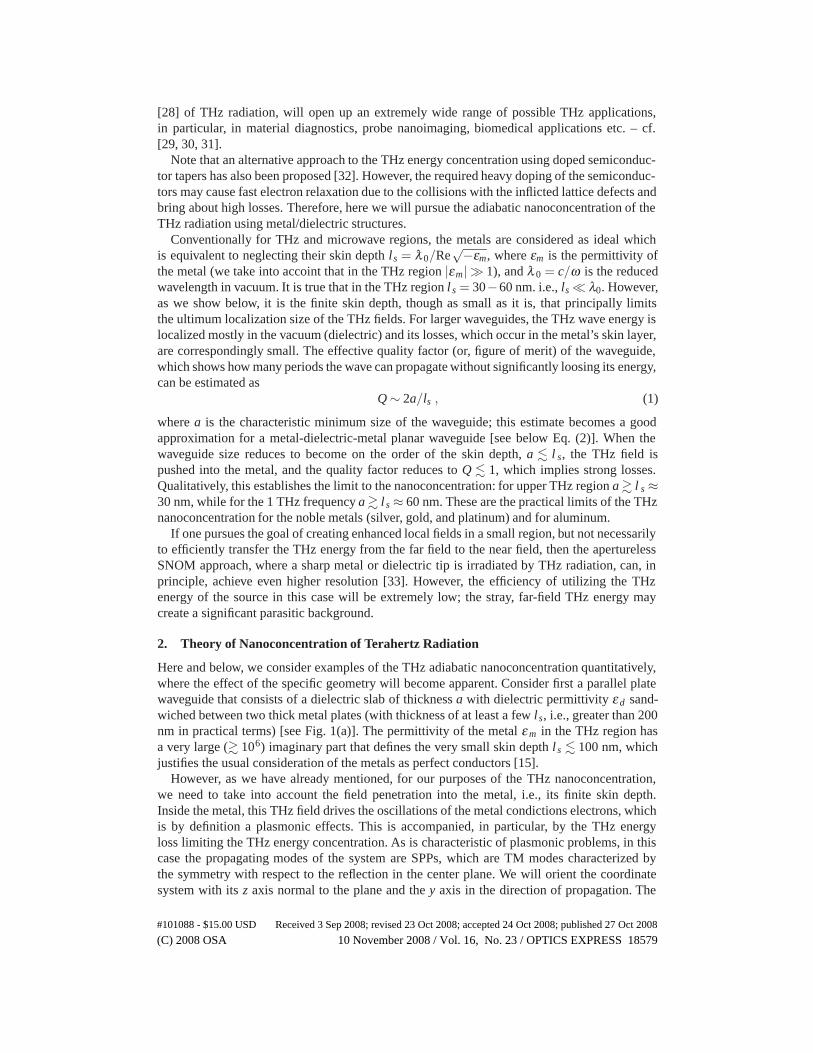
Here and below, we consider examples of the THz adiabatic nanoconcentration quantitatively,where the effect of the specific geometry will become apparent. Consider first a parallel platewaveguide that consists of a dielectric slab of thickness a with dielectric permittivity ε d sand-wiched between two thick metal plates (with thickness of at least a few l s, i.e., greater than 200nm in practical terms) [see Fig. 1(a)]. The permittivity of the metal ε m in the THz region hasa very large (� 106) imaginary part that defines the very small skin depth l s � 100 nm, whichjustifies the usual consideration of the metals as perfect conductors [15].
However, as we have already mentioned, for our purposes of the THz nanoconcentration,we need to take into account the field penetration into the metal, i.e., its finite skin depth.Inside the metal, this THz field drives the oscillations of the metal condictions electrons, whichis by definition a plasmonic effects. This is accompanied, in particular, by the THz energyloss limiting the THz energy concentration. As is characteristic of plasmonic problems, in thiscase the propagating modes of the system are SPPs, which are TM modes characterized bythe symmetry with respect to the reflection in the center plane. We will orient the coordinatesystem with its z axis normal to the plane and the y axis in the direction of propagation. The
(C) 2008 OSA 10 November 2008 / Vol. 16, No. 23 / OPTICS EXPRESS 18579#101088 - $15.00 USD Received 3 Sep 2008; revised 23 Oct 2008; accepted 24 Oct 2008; published 27 Oct 2008
0.2 0.4 0.6 0.8 1
0.5
0
1
1.5
2
Re n
Im n
a (μm)
ls (d)
a
lsfield
(a)
metal
metal
0 500 1000
-300-100
100
300
z (n
m)
y (μm)
Ey
(c) -10-3 10-3
10005000
-5
5
z (μ
m)
y (μm)
Ey
(b) -10-3 10-3
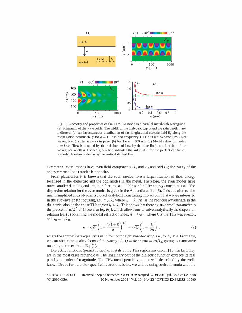
Fig. 1. Geometry and properties of the THz TM mode in a parallel metal-slab waveguide.(a) Schematic of the waveguide. The width of the dielectric gap a and the skin depth ls areindicated. (b) An instantaneous distribution of the longitudinal electric field Ey along thepropagation coordinate y for a = 10 μm and frequency 1 THz in a silver-vacuum-silverwaveguide. (c) The same as in panel (b) but for a = 200 nm. (d) Modal refraction indexn = k/k0 (Ren is denoted by the red line and Imn by the blue line) as a function of thewaveguide width a. Dashed green line indicates the value of n for the perfect conductor.Skin-depth value is shown by the vertical dashed line.
symmetric (even) modes have even field components Hx and Ez and odd Ey; the parity of theantisymmetric (odd) modes is opposite.
From plasmonics it is known that the even modes have a larger fraction of their energylocalized in the dielectric and the odd modes in the metal. Therefore, the even modes havemuch smaller damping and are, therefore, most suitable for the THz energy concentrations. Thedispersion relation for the even modes is given in the Appendix as Eq. (5). This equation can bemuch simplified and solved in a closed analytical form taking into account that we are interestedin the subwavelength focusing, i.e., a � λ , where λ = λ 0/εd is the reduced wavelength in thedielectric; also, in the entire THz region ls � λ . This shows that there exists a small parameter inthe problem lsa/λ 2 � 1 [see also Eq. (6)], which allows one to solve analytically the dispersionrelation Eq. (5) obtaining the modal refraction index n = k/k 0, where k is the THz wavevector,and k0 = 1/λ 0,
n =√
εd
(1+
ls(1+ i)a
)1/2
≈√εd
(1+ i
ls2a
), (2)
where the approximate equality is valid for not too tight nanofocusing, i.e., for l s � a. From this,we can obtain the quality factor of the waveguide Q = Ren/Imn = 2a/l s, giving a quantitativemeaning to the estimate Eq. (1).
Dielectric functions (permittivities) of metals in the THz region are known [15]. In fact, theyare in the most cases rather close. The imaginary part of the dielectric function exceeds its realpart by an order of magnitude. The THz metal permittivitis are well described by the well-known Drude formula. For specific illustrations below we will be using such a formula with the
(C) 2008 OSA 10 November 2008 / Vol. 16, No. 23 / OPTICS EXPRESS 18580#101088 - $15.00 USD Received 3 Sep 2008; revised 23 Oct 2008; accepted 24 Oct 2008; published 27 Oct 2008
parameters for silver from [15].Plasmonic effects (i.e. those of the finite skin depth) are illustrated in Fig. 1 for silver-
vacuum-silver waveguide and frequency of 1 THz. Figs. 1(b) and 1(c) display the longitudi-nal electric field Ey obtained by the exact solution of the Maxwell equations. Note that thisfield component is absent for the ideal conductor; here it is relatively small: on the orderof 10−3 of the transverse field. Fig. 1(b) illustrates the case of a relatively wide waveguide(a = 10 μm), where it is evident that the electric field is localized mostly in the dielectric regionof the waveguide, and the extinction of the wave is small. In a sharp contrast, for a nanoscopicwaveguide (a = 200 nm) in Fig. 1(c), the electric field significantly penetrates the metal. Inaccord with our arguments, there is a very significant extinction of the fields as they propagate;the retardation effects are also evident: the lines of equal amplitude are at an angle relative tothe normal (z) direction. The dependence of the modal refraction index on the thickness a ofthe waveguide obtained from Eq. (2) is plotted in Fig. 1(d). This index increases as a becomescomparable with the skin depth. While Ren and Imn increase by the same absolute amount, thequality factor Q, obviously, greatly decreases with decrease of a. The mode described abovecan be used for broadband energy concentration of THz waves.
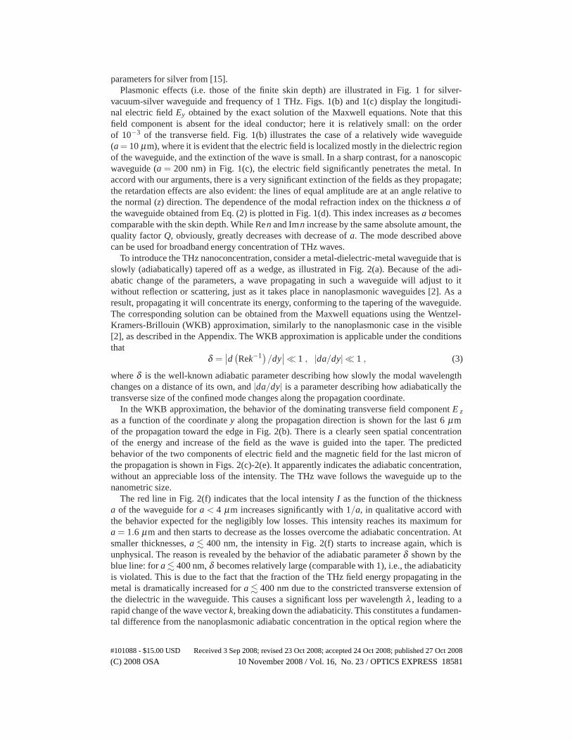
To introduce the THz nanoconcentration, consider a metal-dielectric-metal waveguide that isslowly (adiabatically) tapered off as a wedge, as illustrated in Fig. 2(a). Because of the adi-abatic change of the parameters, a wave propagating in such a waveguide will adjust to itwithout reflection or scattering, just as it takes place in nanoplasmonic waveguides [2]. As aresult, propagating it will concentrate its energy, conforming to the tapering of the waveguide.The corresponding solution can be obtained from the Maxwell equations using the Wentzel-Kramers-Brillouin (WKB) approximation, similarly to the nanoplasmonic case in the visible[2], as described in the Appendix. The WKB approximation is applicable under the conditionsthat
δ =∣∣d (
Rek−1)/dy∣∣ � 1 , |da/dy| � 1 , (3)
where δ is the well-known adiabatic parameter describing how slowly the modal wavelengthchanges on a distance of its own, and |da/dy| is a parameter describing how adiabatically thetransverse size of the confined mode changes along the propagation coordinate.
In the WKB approximation, the behavior of the dominating transverse field component E z
as a function of the coordinate y along the propagation direction is shown for the last 6 μmof the propagation toward the edge in Fig. 2(b). There is a clearly seen spatial concentrationof the energy and increase of the field as the wave is guided into the taper. The predictedbehavior of the two components of electric field and the magnetic field for the last micron ofthe propagation is shown in Figs. 2(c)-2(e). It apparently indicates the adiabatic concentration,without an appreciable loss of the intensity. The THz wave follows the waveguide up to thenanometric size.
The red line in Fig. 2(f) indicates that the local intensity I as the function of the thicknessa of the waveguide for a < 4 μm increases significantly with 1/a, in qualitative accord withthe behavior expected for the negligibly low losses. This intensity reaches its maximum fora = 1.6 μm and then starts to decrease as the losses overcome the adiabatic concentration. Atsmaller thicknesses, a � 400 nm, the intensity in Fig. 2(f) starts to increase again, which isunphysical. The reason is revealed by the behavior of the adiabatic parameter δ shown by theblue line: for a � 400 nm, δ becomes relatively large (comparable with 1), i.e., the adiabaticityis violated. This is due to the fact that the fraction of the THz field energy propagating in themetal is dramatically increased for a � 400 nm due to the constricted transverse extension ofthe dielectric in the waveguide. This causes a significant loss per wavelength λ , leading to arapid change of the wave vector k, breaking down the adiabaticity. This constitutes a fundamen-tal difference from the nanoplasmonic adiabatic concentration in the optical region where the
(C) 2008 OSA 10 November 2008 / Vol. 16, No. 23 / OPTICS EXPRESS 18581#101088 - $15.00 USD Received 3 Sep 2008; revised 23 Oct 2008; accepted 24 Oct 2008; published 27 Oct 2008
adiabatic parameter is constant, and the adiabaticity holds everywhere including the vicinity ofthe tip [2].
To provide for the optimum guiding of the THz wave and its concentration on the nanoscale,the terminating (nanoscopic) part of the waveguide should be tapered slower, in a funnel-likemanner. That is, one needs to decrease the grading da/dy of the waveguide near the edge inorder to keep the adiabaticity parameter δ =
∣∣d (Rek−1
)/da×da/dy
∣∣ approximately constantand small enough to prevent the back-reflection. Because for the adiabatic grading (tapering),the derivative d
(Rek−1
)/da does not depend on the grading (it is the same as for the plane
waveguide) and is only a function of a, the equation δ = δ (y) is a differential equation forthe shape of the waveguide that can be easily integrated. This results in the dependence of thethickness a on the longitudinal coordinate y determined by a simple integral
Ren−1(a) = k0
∫δ (y)dy , (4)
where n(a) is the modal index defined in this case by Eq. (2), and δ (y) is the desired dependenceof the adiabatic parameter along the waveguide, which is an arbitrary function of y satisfyingthe adiabaticity conditions Eq. (3).
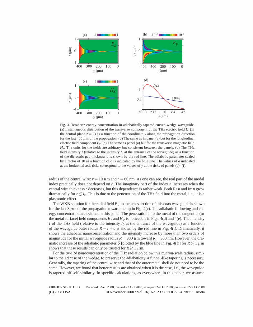
The geometry of an adiabatically-tapered end of the silver/vacuum waveguide found fromEq. (4) and satisfying Eq. (3) and the corresponding WKB solutions for the 1 THz fields areshown in Figs. 3(a)-3(c). The optimum shape of the waveguide in this case is funnel-like, greatlyelongated toward the edge. The nanoconcentration of the field is evident in Figs. 3(a)-3(c), aswell as its penetration into the metal for a � 100 nm. As these panels show quantitatively andthe red curve on Fig. 3(d) qualitatively, the field intensity reaches its maximum at a ≈ 300nm where it is enhanced with respect to the field at the entrance to the funnel waveguide by amodest factor of 1.2. At the same time, the adiabatic parameter δ decreases toward the tip from0.07 to 0.05, indicating the applicability of the WKB approximation everywhere. Note that thisfunnel-shaped wedge, indeed, continues the linearly-graded wedge waveguide shown in Fig. 2,which yields the enhancement factor of ≈ 8 at a = 2 μm. Sequentially, these two waveguidesprovide the intensity enhancement by approximately ×10 while compressing the THz wave tothe thickness of a = 300 nm and the enhancement by a factor of 3 for a = 100 nm.
Thus, true nanolocalization of THz radiation in one dimension (1d) is possible. The minimumtransverse size of this nanolocalization is determined by the skin depth, as we have alreadydiscussed qualitatively in the introductory part of this paper. The obtained 1d beam of thenanoconcentrated THz radiation may be used for different purposes, in particular as a sourcefor the diffraction elements including the nanofocusing zone plates of the type introduced in[34].
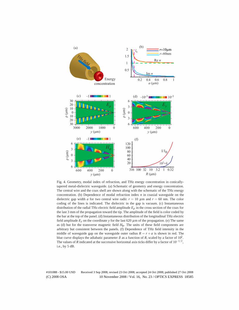
The two-dimensional (2d) concentration of the THz radiation can be achieved by using anadiabatically-tapered conical coax waveguide, whose geometry is illustrated in Fig. 4(a). Thecentral metal wire of radius r is surrounded by a dielectric gap of the radial thickness a, which isenclosed by a thick (∼ 200 nm or thicker) outer metal shell. Both r and a are smooth functionsof the longitudinal coordinate y, which describes the tapering of the coax toward the apex (tip) aty = 0. The THz waves propagate from the wide end of the coax toward the apex, adiabaticallyfollowing the tapering. In the spirit of WKB, for any particular y the wave behavior for thetapered coax is the same as for a cylindrical coax with the values of r and a equal to the localvalues r(y) and a(y).
The dispersion relation for the coax waveguide that takes into account the plasmonic effects(i.e., the penetration of radiation into the metal and the concurrent losses) is obtained in theAppendix as Eq. (9). Calculated from this expression, the dependence of the modal refractiveindex n = k(a,r)/k0 on the dielectric gap a is displayed in Fig. 4(b) for the frequency of 1 THz,silver as a metal, and vacuum in the dielectric gap. The results are shown for two values of the
(C) 2008 OSA 10 November 2008 / Vol. 16, No. 23 / OPTICS EXPRESS 18582#101088 - $15.00 USD Received 3 Sep 2008; revised 23 Oct 2008; accepted 24 Oct 2008; published 27 Oct 2008
θx y
z
THz field concentration
(a)
-2
-1
0
1
2
y (μm)
z (μm
)
(c)
Ez
-1 1
-2-1012
y (μm)
z (μm
)
(d)
Ey
-10-3 103
-2
-1
0
1
2
y (μm)
(e)
z (μm
)
Hx
-1 1
5000 3000 1000-15-10-505
1015
y (μm)
Ez
z (μm
)
(b) -1 1
50 16 5 1.6 0.5 0.16
2468
10
a (μm)
(f)
I/I0
5×δ
158600 400 200 0
600 400 200 0 600 400 200 0
Fig. 2. Adiabatic concentration of THz field energy in a graded waveguide, where a dielec-tric wedge is surrounded by the thick silver layer. (a) Schematic of energy concentration,where θ is the wedge opening angle, the arrow indicates the direction of propagation ofthe THz wave, and the red highlights the area of the adiabatic concentration. The orien-tation of the coordinate system is shown in the inset. (b) An instantaneous distribution ofthe transverse electric field Ez of the THz wave propagating and concentrating along thewedge waveguide for the last 6 mm of the propagation toward the edge. Note the differencein scales in the z and y directions. (c) An instantaneous spatial distribution of the transverseelectric field Ez close to the edge of the wedge, for the last 640 μm of the propagation. (d)The same as (c) but for the longitudinal (with respect to the propagation direction) compo-nent of the field Ey. (e) The same as (c) but for the transverse component of the magneticfield Hx. The units of these field components are arbitrary but consistent between the pan-els. (f) Dependence of THz field intensity in the middle of waveguide on the dielectric gapwidth a (the red line). The blue curve displays the dependence on a of the adiabatic para-meter δ , scaled by a factor of 5. The values of a indicated at the successive horizontal axisticks differ by a factor of 10−1/2, i.e., by 5 dB.
(C) 2008 OSA 10 November 2008 / Vol. 16, No. 23 / OPTICS EXPRESS 18583#101088 - $15.00 USD Received 3 Sep 2008; revised 23 Oct 2008; accepted 24 Oct 2008; published 27 Oct 2008
235 110 64 42
0.5
1
2000
-1
0
1
-1
0
1
0100200300400-1
0
1
a (nm)
(d)I/I0
10×δ
y (μm)z (
μm)
(a) -1 1
Ez
y (μm)
z (μm
)
(c) -1 1
Hx
y (μm)
z (μm
)
(b) -10-3 10-3
Ey
0100200300400
0100200300400
Fig. 3. Terahertz energy concentration in adiabatically tapered curved-wedge waveguide.(a) Instantaneous distribution of the transverse component of the THz electric field Ez (inthe central plane z = 0) as a function of the coordinate y along the propagation directionfor the last 400 μm of the propagation. (b) The same as in panel (a) but for the longitudinalelectric field component Ey. (c) The same as panel (a) but for the transverse magnetic fieldHx. The units for the fields are arbitrary but consistent between the panels. (d) The THzfield intensity I (relative to the intensity I0 at the entrance of the waveguide) as a functionof the dielectric gap thickness a is shown by the red line. The adiabatic parameter scaledby a factor of 10 as a function of a is indicated by the blue line. The values of a indicatedat the horizontal axis ticks correspond to the values of y at the ticks of panels (a)- (f).
radius of the central wire: r = 10 μm and r = 60 nm. As one can see, the real part of the modalindex practically does not depend on r. The imaginary part of the index n increases when thecentral wire thickness r decreases, but this dependence is rather weak. Both Ren and Imn growdramatically for r � ls. This is due to the penetration of the THz field into the metal, i.e., it is aplasmonic effect.
The WKB solution for the radial field Eρ in the cross section of this coax waveguide is shownfor the last 3 μm of the propagation toward the tip in Fig. 4(c). The adiabatic following and en-ergy concentration are evident in this panel. The penetration into the metal of the tangential (tothe metal surface) field components Ey and Hϕ is noticeable in Figs. 4(d) and 4(e). The intensityI of the THz field (relative to the intensity I0 at the entrance of the waveguide) as a functionof the waveguide outer radius R = r + a is shown by the red line in Fig. 4(f). Dramatically, itshows the adiabatic nanoconcentration and the intensity increase by more than two orders ofmagnitude for the initial waveguide radius R = 300 μm toward R = 300 nm. However, the dra-matic increase of the adiabatic parameter δ [plotted by the blue line in Fig. 4(f)] for R � 1 μmshows that these results can only be trusted for R � 1 μm.
For the true 2d nanoconcentration of the THz radiation below this micron-scale radius, simi-lar to the 1d case of the wedge, to preserve the adiabaticity, a funnel-like tapering is necessary.Generally, the tapering of the central wire and that of the outer metal shell do not need to be thesame. However, we found that better results are obtained when it is the case, i.e., the waveguideis tapered-off self-similarly. In specific calculations, as everywhere in this paper, we assume
(C) 2008 OSA 10 November 2008 / Vol. 16, No. 23 / OPTICS EXPRESS 18584#101088 - $15.00 USD Received 3 Sep 2008; revised 23 Oct 2008; accepted 24 Oct 2008; published 27 Oct 2008
3000 2000 1000 0302010
0102030
THz field
Energyconcentration
(a)
0.2 0.4 0.6 0.8 1
0.5
1
1.5
2
Re n
Im n
a (μm)
ls r=10μmr=10μmr=60nm
(b)
6
30
36
y (μm)
ρ (μ
m)
(e) -1 1
Hφ
6
30
36
y (μm)
ρ (μ
m)
(d) -10-3 10-3
y (μm)
ρ (μ
m)
(c) -1 1
Eρ Ey
100 32 10 3.2 1 0.32
20406080
100120
R (μm)
(f)
I/I0
102×δ
316
600 400 200 0
600 400 200 0
Fig. 4. Geometry, modal index of refraction, and THz energy concentration in conically-tapered metal-dielectric waveguide. (a) Schematic of geometry and energy concentration.The central wire and the coax shell are shown along with the schematic of the THz energyconcentration. (b) Dependence of modal refraction index n in coaxial waveguide on thedielectric gap width a for two central wire radii: r = 10 μm and r = 60 nm. The colorcoding of the lines is indicated. The dielectric in the gap is vacuum. (c) Instantaneousdistribution of the radial THz electric field amplitude Eρ in the cross section of the coax forthe last 3 mm of the propagation toward the tip. The amplitude of the field is color coded bythe bar at the top of the panel. (d) Instantaneous distribution of the longitudinal THz electricfield amplitude Ey on the coordinate y for the last 620 μm of the propagation. (e) The sameas (d) but for the transverse magnetic field Hϕ . The units of these field components arearbitrary but consistent between the panels. (f) Dependence of THz field intensity in themiddle of waveguide gap on the waveguide outer radius R = r + a is shown in red. Theblue curve displays the adiabatic parameter δ as a function of R, scaled by a factor of 102.The values of R indicated at the successive horizontal axis ticks differ by a factor of 10−1/2,i.e., by 5 dB.
(C) 2008 OSA 10 November 2008 / Vol. 16, No. 23 / OPTICS EXPRESS 18585#101088 - $15.00 USD Received 3 Sep 2008; revised 23 Oct 2008; accepted 24 Oct 2008; published 27 Oct 2008
400 220 150 110 85 65
12345
1000
02004006002101
2
2101
2
2101
2
y (μm)ρ
(μm
)
(a) -1 1
Eρ
y (μm)
ρ (μ
m)
(b) -10-3 10-3
Ey
y (μm)
(c) -1 1
Hφ
ρ (μ
m)
R (nm)
(d)I/I0
10×δ
0200400600
0200400600
Fig. 5. Adiabatic terahertz energy concentration in a self-similarly curved, funnel-shapedcoaxial waveguide, where the metal is silver, and the dielectric in the gap is vacuum. Thedielectric gap is between the pair of the neighboring curved lines, and the metal is every-where else. (a) Instantaneous distribution of the radial (transverse) component Eρ of theelectric field of the guided THz wave as a function of the propagation coordinate along thewedge y for the last 600 μm of the propagation. (b) The same for the longitudinal elec-tric field component Ey. (c) The same for transverse magnetic field Hϕ , whose lines formcircles around the central metal wire. The units of these field components are arbitrary butconsistent between the panels. (d) The THz intensity I as a function of the waveguide ra-dius R, displayed relative to the intensity I0 at the beginning of the waveguide (red line).Adiabatic parameter δ multiplied by a factor of 10 as a function of R (blue line). The valuesof the radius R shown at the ticks correspond to those of y shown in panels (a)-(c).
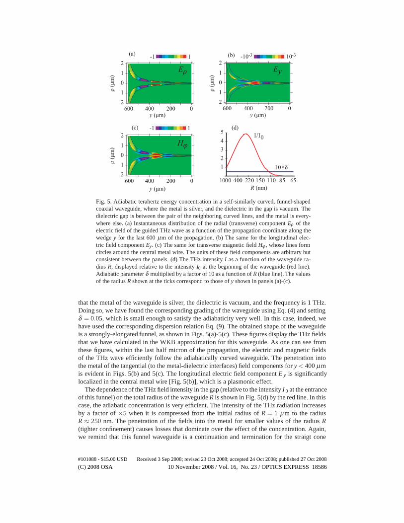
that the metal of the waveguide is silver, the dielectric is vacuum, and the frequency is 1 THz.Doing so, we have found the corresponding grading of the waveguide using Eq. (4) and settingδ = 0.05, which is small enough to satisfy the adiabaticity very well. In this case, indeed, wehave used the corresponding dispersion relation Eq. (9). The obtained shape of the waveguideis a strongly-elongated funnel, as shown in Figs. 5(a)-5(c). These figures display the THz fieldsthat we have calculated in the WKB approximation for this waveguide. As one can see fromthese figures, within the last half micron of the propagation, the electric and magnetic fieldsof the THz wave efficiently follow the adiabatically curved waveguide. The penetration intothe metal of the tangential (to the metal-dielectric interfaces) field components for y < 400 μmis evident in Figs. 5(b) and 5(c). The longitudinal electric field component E y is significantlylocalized in the central metal wire [Fig. 5(b)], which is a plasmonic effect.
The dependence of the THz field intensity in the gap (relative to the intensity I 0 at the entranceof this funnel) on the total radius of the waveguide R is shown in Fig. 5(d) by the red line. In thiscase, the adiabatic concentration is very efficient. The intensity of the THz radiation increasesby a factor of ×5 when it is compressed from the initial radius of R = 1 μm to the radiusR ≈ 250 nm. The penetration of the fields into the metal for smaller values of the radius R(tighter confinement) causes losses that dominate over the effect of the concentration. Again,we remind that this funnel waveguide is a continuation and termination for the straigt cone
(C) 2008 OSA 10 November 2008 / Vol. 16, No. 23 / OPTICS EXPRESS 18586#101088 - $15.00 USD Received 3 Sep 2008; revised 23 Oct 2008; accepted 24 Oct 2008; published 27 Oct 2008
that yields the field enhancement by ×50 for R = 1 μm [see Fig. 4(f)]. Consecutively, thesetwo waveguides (the initial cone continued and terminated by the funnel) are very efficient,adiabatically compressing the THz radiation from the initial radius R = 300 μm to the radiusR = 250 nm increasing its intensity by a factor ×250. Even for the final radius R = 100 nm, thetotal THz intensity is increased by a factor of ×10 (which is the products of factors ×50 for thecone part and ×0.2 for the funnel. Thus, the optimally graded plasmonic-metal 2d waveguideis very efficient in the concentration and guidance of the THz fields with the transverse radiusof confinement R � 100 nm.
3. Conclusion
To discuss the results, we have shown that the THz radiation can be concentrated to the ∼ 100nm transverse size in adiabatically graded plasmonic (metal/dielectric) waveguides. In the op-timum adiabatically-graded, coaxial waveguide, which consists of the initial cone terminatedwith a funnel, the radiation of a 1 THz frequency whose wavelength is 300 μm, can be com-pressed to a spot of 250 nm radius, where its intensity increases by a factor of ×250. Even in thecase of the extreme compression to a spot of the 100 nm radius, the THz intensity is enhancedby one order of magnitude with respect to the initial intensity of the 300 μm spot at the en-trance of the waveguide. The physical process that limits the extent of this spatial concentrationis the skin effect, i.e., penetration of the radiation into the metal that causes the losses: the THzfield penetrates the depth of ls = 30− 60 nm of the metal, which by the order of magnitudedetermines the ultimum localization radius.
The THz nanoconcentration predicted in this paper for optimally-graded adiabatic plasmonicwaveguides provides unique opportunities for THz science and technology, of which we willmention below just a few. The nanoconcentration of the THz radiation will provide the THzultramicroscopy with a THz source of unprecedented spatial resolution and brightness. Theincrease of the THz intensity by two orders of magnitude along with the novel high-power THzsources [26] would allow the observation of a wide range of electronic and vibrational nonlineareffects in metal, semiconductors, insulators, and molecules.
These nonlinear THz phenomena can be used to investigate behavior of various materialsin ultrastrong fields, for nonlinear spectroscopy (including the multidimensional spectroscopy),and for monitoring and detection of various environmental, biological, and chemical objects andthreats such as single bacterial spores and viruses. Such applications will certainly be helpedby very large absorption cross sections of various materials in the THz region. A distinct andsignificant advantage of the adiabatic nanofocusing is that the THz energy is mostly concen-trated in the hollow region of the waveguide, whose size can be made comparable with the sizeof the objects of interest: in the range from 1 micron to 70 nm, which is a typical range forbacteria and their spores, and viruses. This will assure high sensitivity and low background forthe objects that are confined inside these waveguides.
Consider as a specific example the spectroscopy or detection of single particles, such as,e.g., anthrax spores, in the air. A sample containing the suspected nanoparticles in a gas, whichcan be air for the frequencies in the transparency windows, can be pumped through a THzwaveguide, and the detection can be made for each particle in the gas separately on the ba-sis of the two-dimensional nonlinear THz spectra that are expected to be highly informativefor the detection and elimination of the false-positive alarms. Likewise, many other scientific,technological, environmental, and defense applications may become possible.
(C) 2008 OSA 10 November 2008 / Vol. 16, No. 23 / OPTICS EXPRESS 18587#101088 - $15.00 USD Received 3 Sep 2008; revised 23 Oct 2008; accepted 24 Oct 2008; published 27 Oct 2008
Appendix
Terahertz TM Wave in Finite-Conductivity Parallel Plate Waveguide
A parallel plate waveguide supports an even TM mode with wavenumber k, which satisfies thedispersion relation
tanh(κda
2
)= −εdκm
εmκd(5)
where κd =(k2 − εdk2
0
)1/2, κm =
(k2 − εmk2
0
)1/2. In the terahertz range, εm is mainly imaginary,
where Imεm � 1. Therefore, κm ≈ k0√−εm = l−1
s (1− i), where ls = 1/Reκm =√
2/(k0√|εm|)
is the metal skin depth, which is on the order of tens of nanometers. We also assume thatκda � 1, which is always the case for the mode under consideration because either this modeis close to the TEM mode where k = k0εd , or the gap a is thin enough. This leads to a closedexpression for the index of refraction of the mode, which is Eq. (2). Using this, one can check
that κda≈(
εdals/λ 2)1/2
. Consequently, the applicability condition of the approximation used
is (εdals/λ 2
)1/2 � 1 . (6)
This condition is satisfied for the realistic parameters of the problem. For instance, for thefrequency f = 1 THz, the skin depth for metals is l s ≈ 60 nm, while reduced wavelength isλ = 75 μm. The condition Eq. (6) is well satisfied for a � 100 μm, i.e., in the entire range ofinterest to us.
Terahertz TM Wave in Finite-Conductivity Coaxial Waveguide
Consider a coaxial waveguide (coax) with the inner wire radius r and the outer radius R =r +a, where a is the dielectric gap width. The characteristic relation for the TM modes of thiswaveguide has has the following form
(I0(κdr)I0(κmr) − ξ I1(κdr)
I1(κmr)
)(K0(κdR)K0(κmR) − ξ K1(κdR)
K1(κmR)
)= (7)(
K0(κdr)I0(κmr) + ξ K1(κdr)
I1(κmr)
)(I0(κdR)K0(κmR) + ξ I1(κdR)
K1(κmR)
),
where Iν(x) and Kν(x) are modified Bessel functions, and ξ = εdκmεmκd
. This equation is quadratic
with respect to ξ and can be written in the form αξ 2 + β ξ + γ = 0, where the coefficients α ,β , and γ can be easily found by comparison to Eq. (7) as combinations of the Bessel functions.It can obviously be resolved for ξ yielding
β ±√
β 2 −4αγ2α
= −εdκm
εmκd. (8)
In the THz region, only the mode with the minus sign in Eq. (8) propagates. It can be treatedin a manner similar to the mode described by Eq. (5). Eq. (8) can be expanded over the smallparameter κda � 1, and the explicit form of the modal refraction index can be readily obtainedas
n =√
εd
(1+
(I0(κmr)I1(κmr) + K0(κmR)
K1(κmR)
)ls(1+i)
2a
)1/2, (9)
where κm = l−1s (1− i). Similar to the wedge waveguide case, the applicability condition of this
solution is given by Eq. (6).
(C) 2008 OSA 10 November 2008 / Vol. 16, No. 23 / OPTICS EXPRESS 18588#101088 - $15.00 USD Received 3 Sep 2008; revised 23 Oct 2008; accepted 24 Oct 2008; published 27 Oct 2008
WKB Solution for the TM Wave in Graded Waveguide
In the WKB approximation, a solution of the Maxwell equations can be represented as a wavewith amplitude and phase that are slowly varying functions of y on the scale of local wavelength.The behavior in the transverse direction z is the same as for the non-graded system. The WKBsolution is valid if the adiabatic parameter is small
δ = | ddy
1k(y)
| � 1 . (10)
In the WKB approximation, the phase of the mode (eikonal) is given by an integral
φ(y) = k0
∫n(y)dy , (11)
where n(y) is the local refraction index of the mode. The behavior of wave amplitude as afunction of the propagation coordinate y is found from the condition of flux conservation:
vg(y)∫ ∞
−∞W (y,z)dz = const , (12)
where vg(y) = ∂ω/∂k is the wave local group velocity, and W (y,z) is energy density in themode.
Acknowledgements
This work was supported by grants from the Chemical Sciences, Biosciences and GeosciencesDivision of the Office of Basic Energy Sciences, Office of Science, U.S. Department of Energy,a grant CHE-0507147 from NSF, and a grant from the US-Israel BSF. MIS is grateful to S.Gresillon for helpful remarks.
(C) 2008 OSA 10 November 2008 / Vol. 16, No. 23 / OPTICS EXPRESS 18589#101088 - $15.00 USD Received 3 Sep 2008; revised 23 Oct 2008; accepted 24 Oct 2008; published 27 Oct 2008