Embed Size (px)
Citation preview

Purdue UniversityPurdue e-Pubs
Birck and NCN Publications Birck Nanotechnology Center
7-1-2013
Nanoimprinted plasmonic nanocavity arraysSangsik KimBirck Nanotechnology Center, Purdue University, [email protected]
Yi XuanBirck Nanotechnology Center, Purdue University, [email protected]
Vladimir P. DrachevBirck Nanotechnology Center, Purdue University; University of North Texas - Denton, [email protected]
Leo T. VargheseBirck Nanotechnology Center, Purdue University, [email protected]
Li FanBirck Nanotechnology Center, Purdue University, [email protected]
See next page for additional authors
Follow this and additional works at: http://docs.lib.purdue.edu/nanopub
Part of the Nanoscience and Nanotechnology Commons
This document has been made available through Purdue e-Pubs, a service of the Purdue University Libraries. Please contact [email protected] foradditional information.
Kim, Sangsik; Xuan, Yi; Drachev, Vladimir P.; Varghese, Leo T.; Fan, Li; Qi, Minghao; and Webb, Kevin J., "Nanoimprinted plasmonicnanocavity arrays" (2013). Birck and NCN Publications. Paper 1425.http://dx.doi.org/10.1364/OE.21.015081

AuthorsSangsik Kim, Yi Xuan, Vladimir P. Drachev, Leo T. Varghese, Li Fan, Minghao Qi, and Kevin J. Webb
This article is available at Purdue e-Pubs: http://docs.lib.purdue.edu/nanopub/1425

Nanoimprinted plasmonic nanocavityarrays
Sangsik Kim,1 Yi Xuan,1 Vladimir P. Drachev,2 Leo T. Varghese,1 LiFan,1 Minghao Qi,1 and Kevin J. Webb1,∗
1School of Electrical and Computer Engineering and Birck Nanotechnology Center, PurdueUniversity, West Lafayette, IN 47907 USA
2Department of Physics, University of North Texas, Denton, TX 76203, USA∗[email protected]
Abstract: We demonstrate high resonant absorption of visible lightwith a plasmonic nanocavity chain structure fabricated through resistlessnanoimprinting in metal (RNIM). The RNIM approach provides a simple,reproducible, and accurate means to fabricate metallic nanopatterns withhigh fidelity. The nanocavities are shown to be efficiently excited usingnormally incident light, and the resonant wavelength can be controlled byeither the width or the depth of the cavity. Numerical simulations confirmthe experimental observations, and illustrate the behavior of the nanocavitychain waveguide and insensitivity to incident angle. The resonant absorp-tion is due to the excitation of a localized metal-insulator-metal cavitymode. The interacting surface waves allow cavity lengths on the orderof ten nanometers for light having a free space wavelength of about fourhundred nanometers. Coupling of the cavities with an intervening surfaceplasmon wave results in a collective excitation and a chain waveguide modethat should prove valuable for more sensitive detection based on surfaceenhanced Raman scattering.
© 2013 Optical Society of America
OCIS codes: (220.4241) Nanostructure fabrication; (310.6628) Nanostructures; (260.2110)Electromagnetic optics; (350.4238) Nanophotonics and photonic crystals.
References and links1. K. J. Webb and J. Li, “Analysis of transmission through small apertures in conducting films,” Phys. Rev. B 73,
033401 (2006).2. P. Genevet, J. P. Tetienne, E. Gatzogiannis, R. Blanchard, M. A. Kats, M. O. Scully, and F. Capasso, “Large
enhancement of nonlinear optical phenomena by plasmonic nanocavity gratings,” Nano Lett. 10, 4880–4883(2010).
3. N. M. B. Perney, F. J. Garcıa de Abajo, J. J. Baumberg, A. Tang, M. C. Netti, M. D. B. Charlton, and M. E.Zoorob, “Tuning localized plasmon cavities for optimized surface-enhanced Raman scattering,” Phys. Rev. B76, 035426 (2007).
4. H. T. Miyazaki and Y. Kurokawa, “Controlled plasmon resonance in closed metal/insulator/metal nanocavities,”Appl. Phys. Lett. 89, 211126 (2006).
5. Y. Kurokawa and H. T. Miyazaki, “Metal-insulator-metal plasmon nanocavities: Analysis of optical properties,”Phys. Rev. B 75, 035411 (2007).
6. V. J. Sorger, R. F. Oulton, J. Yao, G. Bartal, and X. Zhang, “Plasmonic Fabry-Perot nanocavity,” Nano Lett. 9,3489–3493 (2009).
7. A. Polyakov, S. Cabrini, S. Dhuey, B. Harteneck, P. J. Schuck, and H. A. Padmore, “Plasmonic light trapping innanostructured metal surfaces,” Appl. Phys. Lett. 98, 203104–203106 (2011).
8. A. Polyakov, H. A. Padmore, X. Liang, S. Dhuey, B. Harteneck, J. P. Schuck, and S. Cabrini, “Light trapping inplasmonic nanocavities on metal surfaces,” J. Vac. Sci. Technol. B 29, 06FF01 (2011).
#186800 - $15.00 USD Received 11 Mar 2013; revised 25 Apr 2013; accepted 26 Apr 2013; published 17 Jun 2013(C) 2013 OSA 1 July 2013 | Vol. 21, No. 13 | DOI:10.1364/OE.21.015081 | OPTICS EXPRESS 15081

9. S. Buzzi, F. Robin, V. Callegari, and J. F. Loffler, “Metal direct nanoimprinting for photonics,” Microelectron.Eng. 85, 419–424 (2008).
10. S. Y. Chou, P. R. Krauss, and P. J. Renstrom, “25-nanometer resolution,” Science 272, 85–87 (1996).11. S. H. Ko, I. Park, H. Pan, C. P. Grigoropoulos, A. P. Pisano, C. K. Luscombe, and J. M. J. Frechet, “Direct
nanoimprinting of metal nanoparticles for nanoscale electronics fabrication,” Nano Lett. 7, 1869–1877 (2007).12. A. T. Fafarman, S. H. Hong, H. Caglayan, X. Ye, B. T. Diroll, T. Paik, N. Engheta, C. B. Murray, and C. R.
Kagan, “Chemically tailored dielectric-to-metal transition for the design of metamaterials from nanoimprintedcolloidal nanocrystals,” Nano Lett. 13, 350–357 (2013).
13. H. L. Chen, S. Y. Chuang, H. C. Cheng, C. H. Lin, and T. C. Chu, “Directly patterning metal films by nanoimprintlithography with low-temperature and low-pressure,” Microelectron. Eng. 83, 893–896 (2006).
14. L. T. Varghese, L. Fan, Y. Xuan, C. Tansarawiput, S. Kim, and M. Qi, “Resistless nanoimprinting in metal forplasmonic nanostructures,” Small, http://dx.doi.org/10.1002/smll.201300168 (2013).
15. K. J. Webb and J. Li, “Resonant slot optical guiding in metallic nanoparticle chains,” Phys. Rev. B 72, 201402(2005).
16. E. D. Palik, Handbook of Optical Constants of Solids (Academic Press, 1998) vol. 3.17. J. A. Scholl, A. L. Koh, and J. A. Dionne, “Quantum plasmon resonances of individual metallic nanoparticles,”
Nature 483, 421–427 (2012).18. S. Shivanand, A. Ludwig, and K. J. Webb, “Impact of surface roughness on the effective dielectric constants and
subwavelength image resolution of metal–insulator stack lenses,” Opt. Lett. 37, 4317–4319 (2012).19. K. J. Webb and J. Li, “Resonant waveguide field enhancement in dimers,” Opt. Lett. 31, 3348–3350 (2006).20. J. Homola, S. S. Yee, and G. Gauglitz, “Surface plasmon resonance sensors: review,” Sensor Actuat B-Chem. 54,
3–15 (1999).21. A. Dhawan, M. Canva, and T. Vo-Dinh, “Narrow groove plasmonic nano-gratings for surface plasmon resonance
sensing,” Opt. Express 19, 787–813 (2011).22. H. Liu, Shivanand, and K. J. Webb, “Optical circuits from anisotropic films,” Phys. Rev. B 79, 094203 (2009).23. E. M. Purcell, “Spontaneous emission probabilities at radio frequencies,” Phys. Rev. B 69, 681 (1946).24. H. Altug, D. Englund, and J. Vuckovic, “Ultrafast photonic crystal nanocavity laser,” Nat. Phys. 2, 484–488
(2006).
1. Introduction
Noble metals are good plasmonic materials, and they offer a complex dielectric constant at vis-ible wavelengths with a relatively small imaginary component and a negative real part that pro-vides for transverse magnetic surface waves. The collective oscillation of photons and electronsforms a surface plasmon-polariton wave, and coupling of two surfaces as a metal-insulator-metal (MIM) waveguide mode allows the squeezing of light down to the subwavelength lengthscale and large field enhancement in small cavities [1]. With visible light, cavity dimensionscan be just a few tens of nanometers or less, and a footprint on the scale of current CMOStechnology becomes possible. The field enhancement within a small mode volume makes thesurface plasmon desirable in nonlinear optics [2] and for surface enhanced Raman scattering(SERS) [3]. More generally, plasmonic nanocavities provide sensing opportunities and the ba-sis for nanolaser sources and for detectors, with the incorporation of appropriate materials intothe cavities. The challenge is a suitable fabrication method to achieve adequate fabrication tol-erances and suitable material arrangements for specific applications.
Several fabrication schemes have been used to realize plasmonic cavity structures [4–8]. Acavity formed with a MIM waveguide was demonstrated by depositing Au/SiO2/Au films andusing focused ion beam (FIB) milling to form a ridge [4, 5]. However, use of a gap filling ma-terial (or support material, on the order of 10 nm of SiO2 in this case) restricts nonlinear opticsand SERS applications. While FIB can be used to pattern metals by using a heavy ion to bom-bard and form features, it is a relatively time consuming process and has limited resolution.For nanostructures, electron beam lithography (EBL) is widely used for its high resolution pat-terning. Using EBL, a surface wave (metal - free space) cavity was achieved with two verticalAg fins that act as mirrors [6]. Here, electroplated Ag was deposited over EBL patterned resistfollowed by lift-off. In this case, they achieved quality factor (Q ≈ λ0/Δλ , where λ0 is the freespace resonant wavelength and Δλ is the 3-dB bandwidth of the resonance) ranging from 100 to
#186800 - $15.00 USD Received 11 Mar 2013; revised 25 Apr 2013; accepted 26 Apr 2013; published 17 Jun 2013(C) 2013 OSA 1 July 2013 | Vol. 21, No. 13 | DOI:10.1364/OE.21.015081 | OPTICS EXPRESS 15082

200. The dimension of the structure was dictated by the wavelength of the surface wave, whichis close to the free space wavelength. Moreover, free space coupling remains a challenge. Re-cently, plasmonic light trapping in narrow nanogrooves on a metal surface was demonstratedby evaporating gold onto patterned hydrogen silsesquioxane (HSQ) resist lines [7, 8]. The pat-terned Au film was separated from the substrate either through wafer back-etching [7] or bypeeling it off using epoxy [8]. Evaporating metal films over patterned resists often suffer fromvoid formation due to a self shadowing effect. Also, it requires the complete back-etching ofthe primary substrate. In contrast, nanoimprint lithography can be used to pattern metal filmswith much ease and versatility.
It is well known that metal films can be shaped to the desired pattern by using ultra-high pres-sure and high temperature [9]. However, the use of extreme conditions is undesirable and notsuitable for wafer-based processing. An alternative to this is nanoimprint lithography, where amold is used to mechanically deform a soft material by applying low pressure and low tempera-ture [10]. While this has normally been used to pattern polymer resists, it has also been usedto directly pattern colloidal Au nanoparticles, allowing feature sizes down to about 100 nm tobe achieved [11, 12]. This method provided a convenient fabrication approach to pattern vari-ous wire and dot structures for resistors and transistors [11], and for metamaterials [12]. Whilecolloidal metal nanoparticles can be easily formed into shapes, metal films are difficult to bepatterned, owing to their higher elastic modulus and hardness. To counter this, a soft intermedi-ate layer has been added between the substrate and the metal film to realize metal patterns withgentle contours using low pressure and low temperature [13]. However, many high performanceplasmonic devices require high quality noble metal surfaces with precise features. Hence, it isimportant to use a low pressure and low temperature process that forms patterns on high qualitymetal films without any intermediate layers.
In this work, we demonstrate a plasmonic nanocavity chain structure using resistless nanoim-printing in metal (RNIM) [14]. A Si mold with sparse nanoscale patterns is used to directlyimprint Ag films in a single step using low pressure/temperature to fabricate devices with highthroughput and low-cost. With etching techniques for Si being well developed, RNIM allowsnanoscale resolution and sharp features in Si to be realized on metal through its high fidelity pat-tern transfer. The experimental results for the nanocavity chain structures fabricated by RNIMare supported by numerical simulations. The structure shows polarization sensitive and angu-lar insensitive absorption, and has high field enhancement within the nanometer-scale cavitydimensionsshows the RNIM process flow.
2. Device fabrication
Figure 1 shows the RNIM process flow. The mold was fabricated on a Si wafer by using EBL(100 kV). HSQ, a negative EBL resist, was spun to a thickness of 50 nm on a Si wafer, exposedand developed. The HSQ patterns were transferred to Si using reactive ion etching (RIE) withCl2/Ar chemistry, and HSQ was removed with a brief dip in HF acid to form the mold. A 5nm Cr layer was deposited on a quartz substrate to promote adhesion, and then a Ag film wasdeposited with an electron beam evaporator. Before nanoimprinting, the mold was cleaned by astandard RCA process, while the metal film was sonicated in a solvent. RNIM was performedon a Nanonex NX 2000, a commercial resist-based nanoimprint lithography tool, by applyinga pressure of 4 MPa and with temperatures between 100 and 150 ◦C. After nanoimprinting, themold and substrate were manually separated.
Figure 2(a) shows a Si mold and the resulting imprint on a 200 nm thick Ag film is shown inFig. 2(b). The grating and grid patterns of the mold pressed into the Ag film result in square dotarrays and ridges. The Si gratings shown in Fig. 2(c) were imprinted into a Ag film, resulting inthe Ag gratings shown in Fig. 2(d). The sharp edges of the imprinted metal pattern shows the
#186800 - $15.00 USD Received 11 Mar 2013; revised 25 Apr 2013; accepted 26 Apr 2013; published 17 Jun 2013(C) 2013 OSA 1 July 2013 | Vol. 21, No. 13 | DOI:10.1364/OE.21.015081 | OPTICS EXPRESS 15083
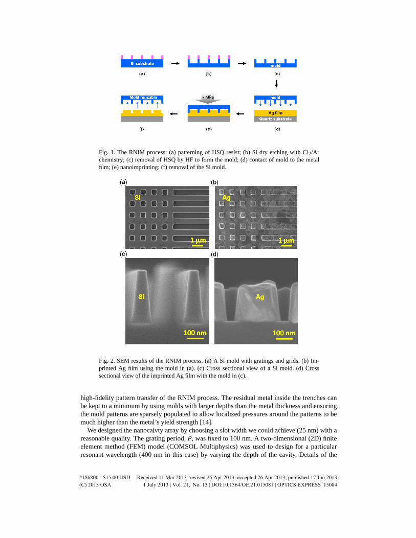
Fig. 1. The RNIM process: (a) patterning of HSQ resist; (b) Si dry etching with Cl2/Archemistry; (c) removal of HSQ by HF to form the mold; (d) contact of mold to the metalfilm; (e) nanoimprinting; (f) removal of the Si mold.
Fig. 2. SEM results of the RNIM process. (a) A Si mold with gratings and grids. (b) Im-printed Ag film using the mold in (a). (c) Cross sectional view of a Si mold. (d) Crosssectional view of the imprinted Ag film with the mold in (c).
high-fidelity pattern transfer of the RNIM process. The residual metal inside the trenches canbe kept to a minimum by using molds with larger depths than the metal thickness and ensuringthe mold patterns are sparsely populated to allow localized pressures around the patterns to bemuch higher than the metal’s yield strength [14].
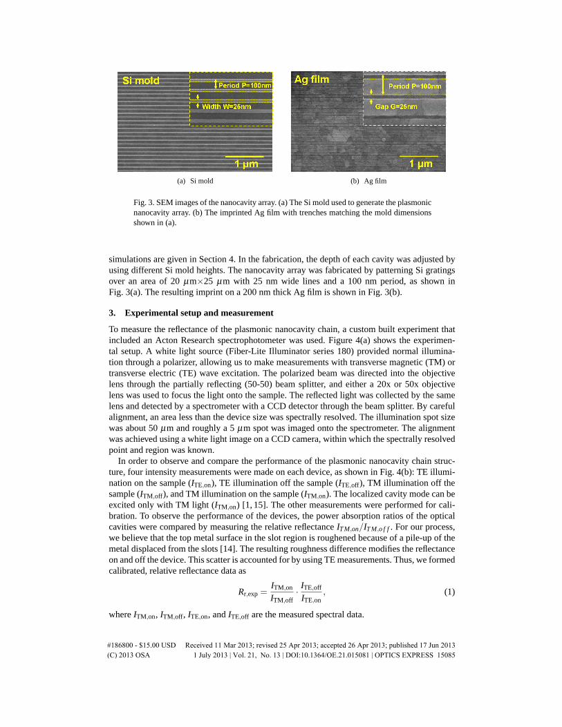
We designed the nanocaivty array by choosing a slot width we could achieve (25 nm) with areasonable quality. The grating period, P, was fixed to 100 nm. A two-dimensional (2D) finiteelement method (FEM) model (COMSOL Multiphysics) was used to design for a particularresonant wavelength (400 nm in this case) by varying the depth of the cavity. Details of the
#186800 - $15.00 USD Received 11 Mar 2013; revised 25 Apr 2013; accepted 26 Apr 2013; published 17 Jun 2013(C) 2013 OSA 1 July 2013 | Vol. 21, No. 13 | DOI:10.1364/OE.21.015081 | OPTICS EXPRESS 15084
(a) Si mold (b) Ag film
Fig. 3. SEM images of the nanocavity array. (a) The Si mold used to generate the plasmonicnanocavity array. (b) The imprinted Ag film with trenches matching the mold dimensionsshown in (a).
simulations are given in Section 4. In the fabrication, the depth of each cavity was adjusted byusing different Si mold heights. The nanocavity array was fabricated by patterning Si gratingsover an area of 20 μm×25 μm with 25 nm wide lines and a 100 nm period, as shown inFig. 3(a). The resulting imprint on a 200 nm thick Ag film is shown in Fig. 3(b).
3. Experimental setup and measurement
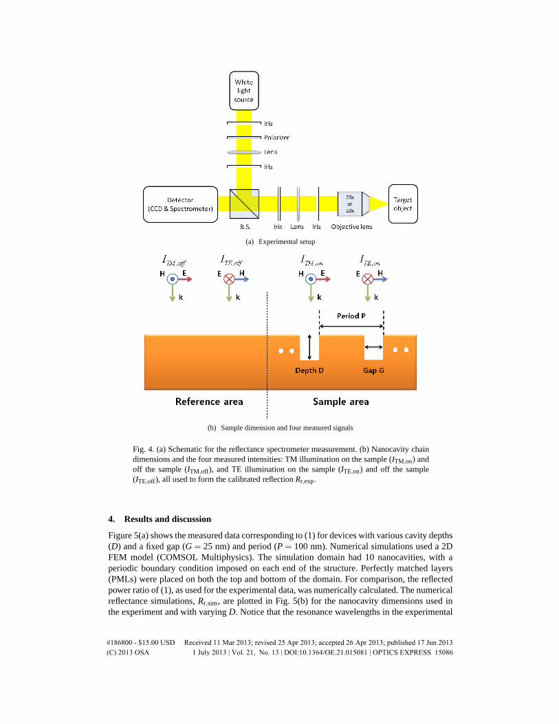
To measure the reflectance of the plasmonic nanocavity chain, a custom built experiment thatincluded an Acton Research spectrophotometer was used. Figure 4(a) shows the experimen-tal setup. A white light source (Fiber-Lite Illuminator series 180) provided normal illumina-tion through a polarizer, allowing us to make measurements with transverse magnetic (TM) ortransverse electric (TE) wave excitation. The polarized beam was directed into the objectivelens through the partially reflecting (50-50) beam splitter, and either a 20x or 50x objectivelens was used to focus the light onto the sample. The reflected light was collected by the samelens and detected by a spectrometer with a CCD detector through the beam splitter. By carefulalignment, an area less than the device size was spectrally resolved. The illumination spot sizewas about 50 μm and roughly a 5 μm spot was imaged onto the spectrometer. The alignmentwas achieved using a white light image on a CCD camera, within which the spectrally resolvedpoint and region was known.
In order to observe and compare the performance of the plasmonic nanocavity chain struc-ture, four intensity measurements were made on each device, as shown in Fig. 4(b): TE illumi-nation on the sample (ITE,on), TE illumination off the sample (ITE,off), TM illumination off thesample (ITM,off), and TM illumination on the sample (ITM,on). The localized cavity mode can beexcited only with TM light (ITM,on) [1, 15]. The other measurements were performed for cali-bration. To observe the performance of the devices, the power absorption ratios of the opticalcavities were compared by measuring the relative reflectance ITM,on/ITM,o f f . For our process,we believe that the top metal surface in the slot region is roughened because of a pile-up of themetal displaced from the slots [14]. The resulting roughness difference modifies the reflectanceon and off the device. This scatter is accounted for by using TE measurements. Thus, we formedcalibrated, relative reflectance data as
Rr,exp =ITM,on
ITM,off· ITE,off
ITE,on, (1)
where ITM,on, ITM,off, ITE,on, and ITE,off are the measured spectral data.
#186800 - $15.00 USD Received 11 Mar 2013; revised 25 Apr 2013; accepted 26 Apr 2013; published 17 Jun 2013(C) 2013 OSA 1 July 2013 | Vol. 21, No. 13 | DOI:10.1364/OE.21.015081 | OPTICS EXPRESS 15085
(a) Experimental setup
(b) Sample dimension and four measured signals
Fig. 4. (a) Schematic for the reflectance spectrometer measurement. (b) Nanocavity chaindimensions and the four measured intensities: TM illumination on the sample (ITM,on) andoff the sample (ITM,off), and TE illumination on the sample (ITE,on) and off the sample(ITE,off), all used to form the calibrated reflection Rr,exp.
4. Results and discussion
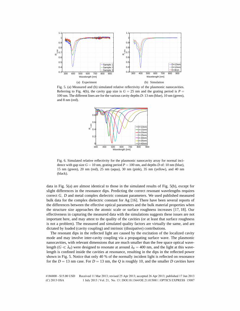
Figure 5(a) shows the measured data corresponding to (1) for devices with various cavity depths(D) and a fixed gap (G = 25 nm) and period (P = 100 nm). Numerical simulations used a 2DFEM model (COMSOL Multiphysics). The simulation domain had 10 nanocavities, with aperiodic boundary condition imposed on each end of the structure. Perfectly matched layers(PMLs) were placed on both the top and bottom of the domain. For comparison, the reflectedpower ratio of (1), as used for the experimental data, was numerically calculated. The numericalreflectance simulations, Rr,sim, are plotted in Fig. 5(b) for the nanocavity dimensions used inthe experiment and with varying D. Notice that the resonance wavelengths in the experimental
#186800 - $15.00 USD Received 11 Mar 2013; revised 25 Apr 2013; accepted 26 Apr 2013; published 17 Jun 2013(C) 2013 OSA 1 July 2013 | Vol. 21, No. 13 | DOI:10.1364/OE.21.015081 | OPTICS EXPRESS 15086
300 400 500 600 700 800 9000.3
0.4
0.5
0.6
0.7
0.8
0.9
1
1.1
Wavelength [nm]
Rr,
exp
Sample 1Sample 2Sample 3
(a) Experiment
300 400 500 600 700 800 9000.3
0.4
0.5
0.6
0.7
0.8
0.9
1
1.1
Wavelength [nm]
Rr,
sim
D=13nmD=10nmD=8nm
(b) Simulation
Fig. 5. (a) Measured and (b) simulated relative reflectivity of the plasmonic nanocavities.Referring to Fig. 4(b), the cavity gap size is G = 25 nm and the grating period is P =100 nm. The different lines are for the various cavity depths D: 13 nm (blue), 10 nm (green),and 8 nm (red).
300 400 500 600 700 800 9000
0.2
0.4
0.6
0.8
1
Wavelength [nm]
Rr,
sim
D=10nmD=15nmD=20nmD=25nmD=30nmD=35nmD=40nm
Fig. 6. Simulated relative reflectivity for the plasmonic nanocavity array for normal inci-dence with gap size G = 10 nm, grating period P = 100 nm, and depths D of: 10 nm (blue),15 nm (green), 20 nm (red), 25 nm (aqua), 30 nm (pink), 35 nm (yellow), and 40 nm(black).
data in Fig. 5(a) are almost identical to those in the simulated results of Fig. 5(b), except forslight differences in the resonance dips. Predicting the correct resonant wavelengths requirescorrect G, D and metal complex dielectric constant parameters. We used published measuredbulk data for the complex dielectric constant for Ag [16]. There have been several reports ofthe differences between the effective optical parameters and the bulk material properties whenthe structure size approaches the atomic scale or surface roughness increases [17, 18]. Oureffectiveness in capturing the measured data with the simulations suggests these issues are notimportant here, and may attest to the quality of the cavities (or at least that surface roughnessis not a problem). The measured and simulated quality factors are virtually the same, and aredictated by loaded (cavity coupling) and intrinsic (dissipative) contributions.
The resonant dips in the reflected light are caused by the excitation of the localized cavitymode and may involve inter-cavity coupling via a propagating surface wave. The plasmonicnanocavities, with relevant dimensions that are much smaller than the free space optical wave-length (G � λ0) were designed to resonate at around λ0 = 400 nm, and the light at this wave-length is confined inside the cavities at resonance, resulting in the dips in the reflected powershown in Fig. 5. Notice that only 40 % of the normally incident light is reflected on resonancefor the D = 13 nm case. For D = 13 nm, the Q is roughly 10, and the smaller D cavities have
#186800 - $15.00 USD Received 11 Mar 2013; revised 25 Apr 2013; accepted 26 Apr 2013; published 17 Jun 2013(C) 2013 OSA 1 July 2013 | Vol. 21, No. 13 | DOI:10.1364/OE.21.015081 | OPTICS EXPRESS 15087
(a) Color contours: normalized |Hz|, Arrows: Poynt-ing vector
−800 −600 −400 −200 0 200 400 600 8000.21
0.22
0.23
0.24
0.25
0.26
x [nm]
Nor
mal
ized
⏐H
z⏐
y=50nm
(b) Normalized |Hz(x)| at y = 50 nm
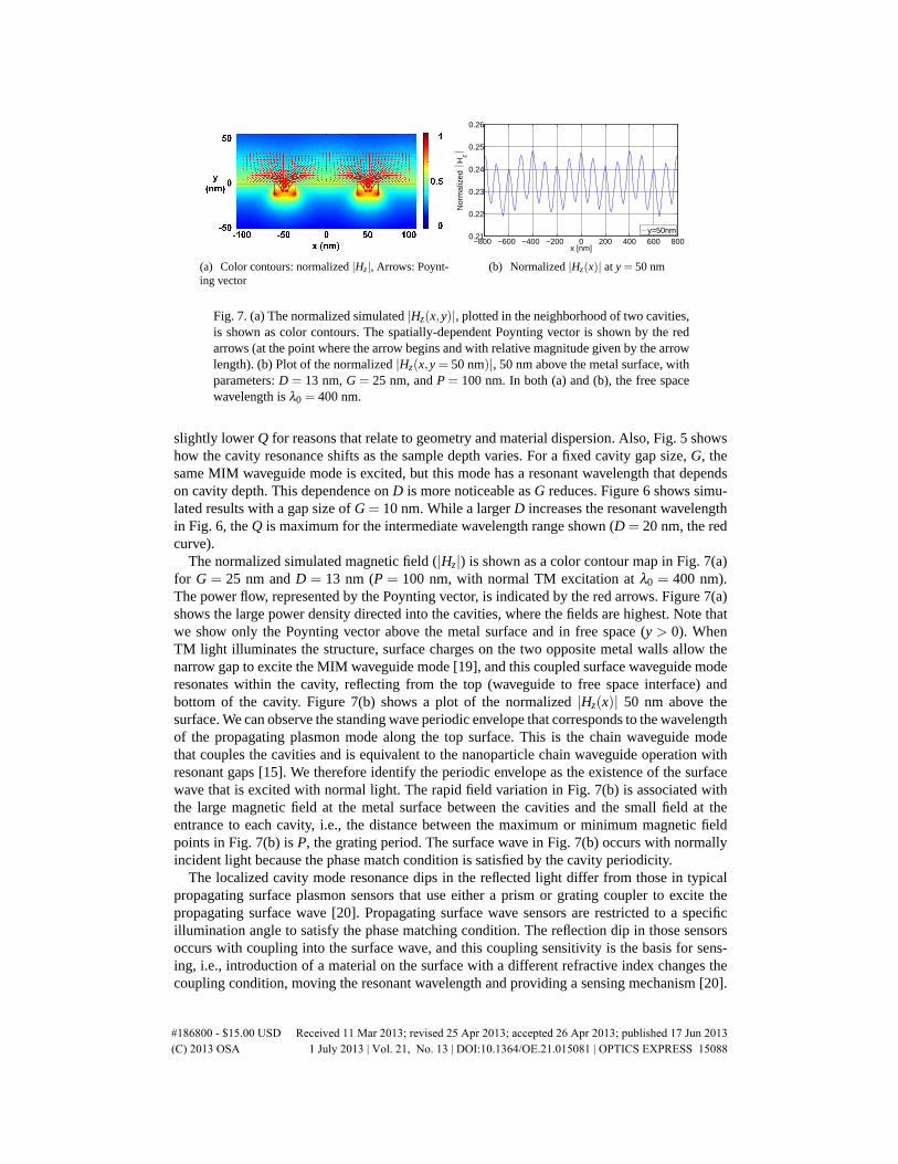
Fig. 7. (a) The normalized simulated |Hz(x,y)|, plotted in the neighborhood of two cavities,is shown as color contours. The spatially-dependent Poynting vector is shown by the redarrows (at the point where the arrow begins and with relative magnitude given by the arrowlength). (b) Plot of the normalized |Hz(x,y = 50 nm)|, 50 nm above the metal surface, withparameters: D = 13 nm, G = 25 nm, and P = 100 nm. In both (a) and (b), the free spacewavelength is λ0 = 400 nm.
slightly lower Q for reasons that relate to geometry and material dispersion. Also, Fig. 5 showshow the cavity resonance shifts as the sample depth varies. For a fixed cavity gap size, G, thesame MIM waveguide mode is excited, but this mode has a resonant wavelength that dependson cavity depth. This dependence on D is more noticeable as G reduces. Figure 6 shows simu-lated results with a gap size of G = 10 nm. While a larger D increases the resonant wavelengthin Fig. 6, the Q is maximum for the intermediate wavelength range shown (D = 20 nm, the redcurve).
The normalized simulated magnetic field (|Hz|) is shown as a color contour map in Fig. 7(a)for G = 25 nm and D = 13 nm (P = 100 nm, with normal TM excitation at λ0 = 400 nm).The power flow, represented by the Poynting vector, is indicated by the red arrows. Figure 7(a)shows the large power density directed into the cavities, where the fields are highest. Note thatwe show only the Poynting vector above the metal surface and in free space (y > 0). WhenTM light illuminates the structure, surface charges on the two opposite metal walls allow thenarrow gap to excite the MIM waveguide mode [19], and this coupled surface waveguide moderesonates within the cavity, reflecting from the top (waveguide to free space interface) andbottom of the cavity. Figure 7(b) shows a plot of the normalized |Hz(x)| 50 nm above thesurface. We can observe the standing wave periodic envelope that corresponds to the wavelengthof the propagating plasmon mode along the top surface. This is the chain waveguide modethat couples the cavities and is equivalent to the nanoparticle chain waveguide operation withresonant gaps [15]. We therefore identify the periodic envelope as the existence of the surfacewave that is excited with normal light. The rapid field variation in Fig. 7(b) is associated withthe large magnetic field at the metal surface between the cavities and the small field at theentrance to each cavity, i.e., the distance between the maximum or minimum magnetic fieldpoints in Fig. 7(b) is P, the grating period. The surface wave in Fig. 7(b) occurs with normallyincident light because the phase match condition is satisfied by the cavity periodicity.
The localized cavity mode resonance dips in the reflected light differ from those in typicalpropagating surface plasmon sensors that use either a prism or grating coupler to excite thepropagating surface wave [20]. Propagating surface wave sensors are restricted to a specificillumination angle to satisfy the phase matching condition. The reflection dip in those sensorsoccurs with coupling into the surface wave, and this coupling sensitivity is the basis for sens-ing, i.e., introduction of a material on the surface with a different refractive index changes thecoupling condition, moving the resonant wavelength and providing a sensing mechanism [20].
#186800 - $15.00 USD Received 11 Mar 2013; revised 25 Apr 2013; accepted 26 Apr 2013; published 17 Jun 2013(C) 2013 OSA 1 July 2013 | Vol. 21, No. 13 | DOI:10.1364/OE.21.015081 | OPTICS EXPRESS 15088
0 10 20 30 40 50 60 700
0.2
0.4
0.6
0.8
1
Incidence angle [deg]
Rr,
sim
G=10, D=20nm, P=100nm, λ0=500nm
(a)
300 400 500 600 700 800 9000
0.2
0.4
0.6
0.8
1
Wavelength [nm]
Rr,
sim
θinc
=0°
θinc
=30°
θinc
=60°
(b)
Fig. 8. (a) Simulated relative reflectivity for the plasmonic nanocavity array for TM lightat λ0 = 500 nm as a function of incidence angle (θinc) with a gap size G = 10 nm, agrating period P = 100 nm, and a depth D = 20 nm. (b) The same calculation as (a), butas a function of excitation wavelength for different illumination angles: θinc = 0◦ (blue),θinc = 30◦ (green), and θinc = 60◦ (red).
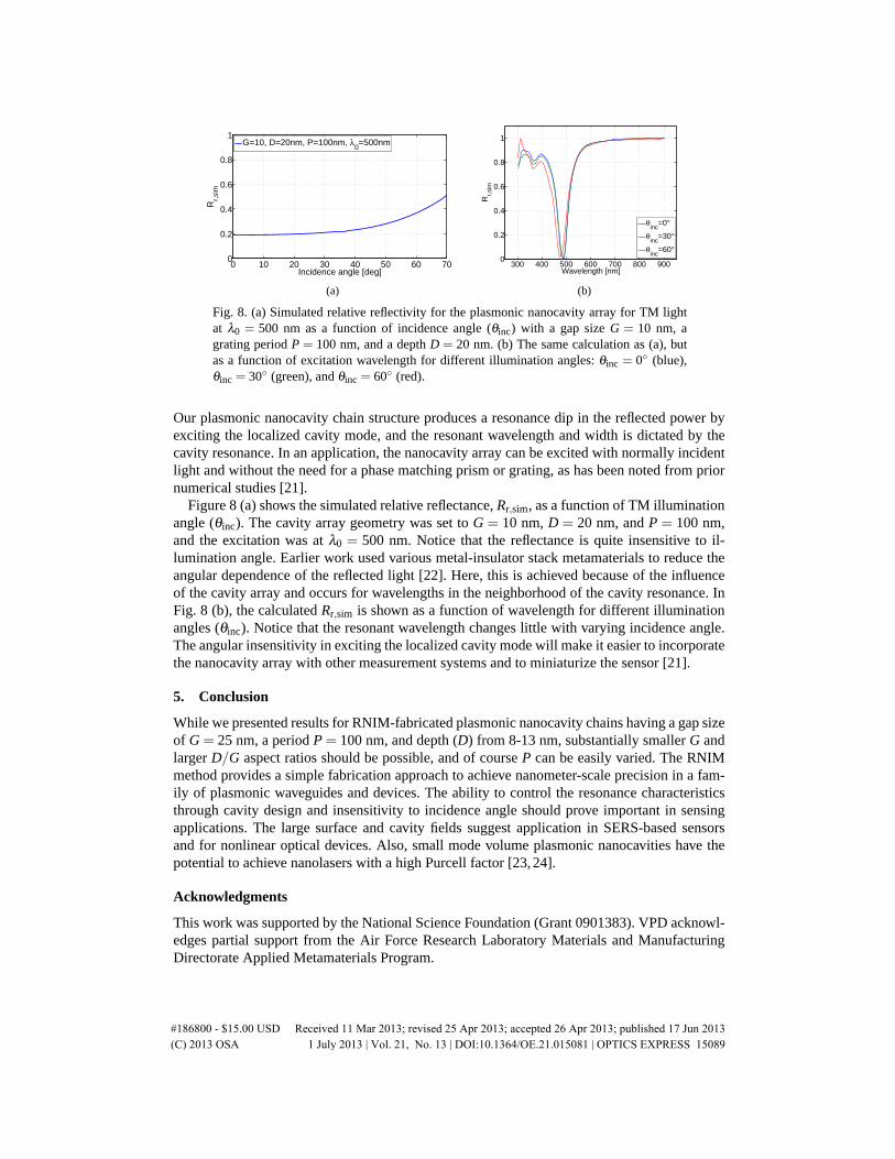
Our plasmonic nanocavity chain structure produces a resonance dip in the reflected power byexciting the localized cavity mode, and the resonant wavelength and width is dictated by thecavity resonance. In an application, the nanocavity array can be excited with normally incidentlight and without the need for a phase matching prism or grating, as has been noted from priornumerical studies [21].
Figure 8 (a) shows the simulated relative reflectance, Rr,sim, as a function of TM illuminationangle (θinc). The cavity array geometry was set to G = 10 nm, D = 20 nm, and P = 100 nm,and the excitation was at λ0 = 500 nm. Notice that the reflectance is quite insensitive to il-lumination angle. Earlier work used various metal-insulator stack metamaterials to reduce theangular dependence of the reflected light [22]. Here, this is achieved because of the influenceof the cavity array and occurs for wavelengths in the neighborhood of the cavity resonance. InFig. 8 (b), the calculated Rr,sim is shown as a function of wavelength for different illuminationangles (θinc). Notice that the resonant wavelength changes little with varying incidence angle.The angular insensitivity in exciting the localized cavity mode will make it easier to incorporatethe nanocavity array with other measurement systems and to miniaturize the sensor [21].
5. Conclusion
While we presented results for RNIM-fabricated plasmonic nanocavity chains having a gap sizeof G = 25 nm, a period P = 100 nm, and depth (D) from 8-13 nm, substantially smaller G andlarger D/G aspect ratios should be possible, and of course P can be easily varied. The RNIMmethod provides a simple fabrication approach to achieve nanometer-scale precision in a fam-ily of plasmonic waveguides and devices. The ability to control the resonance characteristicsthrough cavity design and insensitivity to incidence angle should prove important in sensingapplications. The large surface and cavity fields suggest application in SERS-based sensorsand for nonlinear optical devices. Also, small mode volume plasmonic nanocavities have thepotential to achieve nanolasers with a high Purcell factor [23, 24].
Acknowledgments
This work was supported by the National Science Foundation (Grant 0901383). VPD acknowl-edges partial support from the Air Force Research Laboratory Materials and ManufacturingDirectorate Applied Metamaterials Program.
#186800 - $15.00 USD Received 11 Mar 2013; revised 25 Apr 2013; accepted 26 Apr 2013; published 17 Jun 2013(C) 2013 OSA 1 July 2013 | Vol. 21, No. 13 | DOI:10.1364/OE.21.015081 | OPTICS EXPRESS 15089