Embed Size (px)
Citation preview

8/13/2019 Metallization Lecture
http://slidepdf.com/reader/full/metallization-lecture 1/30
Metallization – deposition and
etching
Material mainly taken from Campbell, UCCS

8/13/2019 Metallization Lecture
http://slidepdf.com/reader/full/metallization-lecture 2/30
Application
• Metallization is back-end processing
• Metals used are aluminum and copper
• Mainly involves deposition and etching, also planarization
• Similar (but typically less complicated) process flows as in
front-end processing

8/13/2019 Metallization Lecture
http://slidepdf.com/reader/full/metallization-lecture 3/30
6 metal level copper dual damascene process crossection at 0.18µm node (R. DeJule, “Dual-damascene:
overcoming process issues”, Semiconductor International, pp. 94, June 2000)

8/13/2019 Metallization Lecture
http://slidepdf.com/reader/full/metallization-lecture 4/30
3D SEM of 9 metal level Cu process (H. Ruelke, C. Streck, M. -Van. Ngo, L. You, S. Weiher-Telford, O.
Chretien, J. Matusche, D. Dugiarto, J. Sabharwal, “Manufacturing implementation of low-k dielectrics for
copper damascene technology”, Advanced Semiconductor Manufacturing Conference, pp. 356–9, 2002.)
8/13/2019 Metallization Lecture
http://slidepdf.com/reader/full/metallization-lecture 5/30
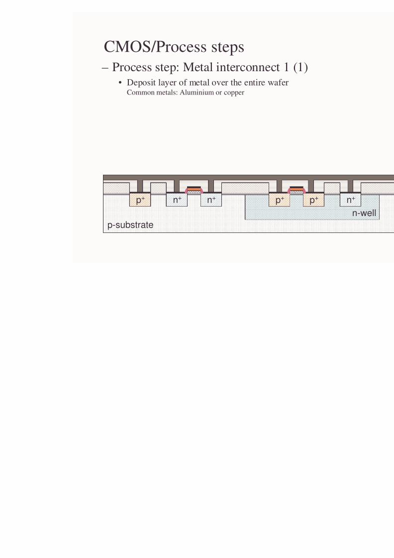
CMOS/Process steps– Process step: Metal interconnect 1 (1)
• Deposit layer of metal over the entire waferCommon metals: Aluminium or copper
p+ p+ p+n+ n+

8/13/2019 Metallization Lecture
http://slidepdf.com/reader/full/metallization-lecture 6/30
CMOS/Process steps– Process step: Metal interconnect 1 (2)
• Photolithography sequence using “Metal 1 mask”
• Metal selectively etched
p+ p+ p+n+ n+

8/13/2019 Metallization Lecture
http://slidepdf.com/reader/full/metallization-lecture 7/30
CMOS/Process steps– Process step: Via windows
• Cover wafer with a layer of SiN3
• Lithography using the “via mask”• Plasma etching
p+ p+ p+n+ n+
8/13/2019 Metallization Lecture
http://slidepdf.com/reader/full/metallization-lecture 8/30
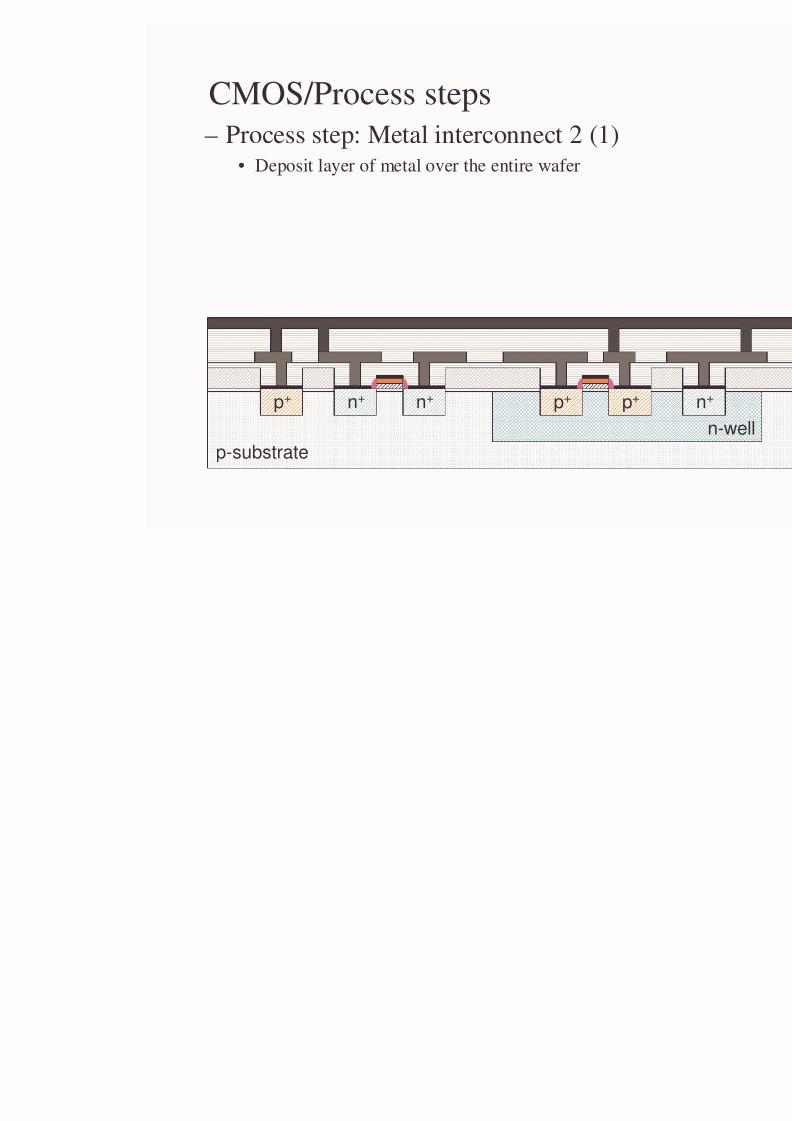
CMOS/Process steps– Process step: Metal interconnect 2 (1)
• Deposit layer of metal over the entire wafer
p+ p+ p+n+ n+
8/13/2019 Metallization Lecture
http://slidepdf.com/reader/full/metallization-lecture 9/30
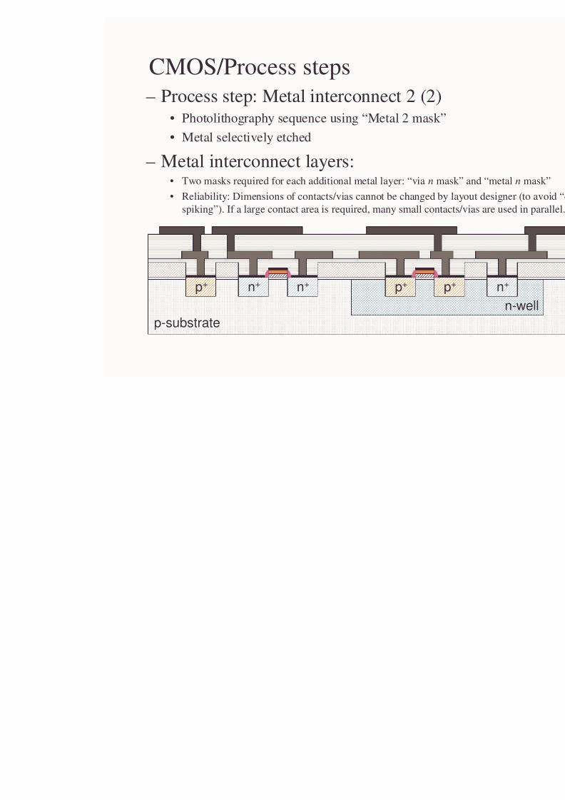
CMOS/Process steps– Process step: Metal interconnect 2 (2)
• Photolithography sequence using “Metal 2 mask”
• Metal selectively etched
– Metal interconnect layers:• Two masks required for each additional metal layer: “via n mask” and
• Reliability: Dimensions of contacts/vias cannot be changed by layout
spiking”). If a large contact area is required, many small contacts/vias
p+ p+ p+n+ n+

8/13/2019 Metallization Lecture
http://slidepdf.com/reader/full/metallization-lecture 10/30

8/13/2019 Metallization Lecture
http://slidepdf.com/reader/full/metallization-lecture 11/30
• Chemical deposition techniques exploit the creation ofsolid materials directly from chemical reactions in gas
and/or liquid compositions or with the substrate material.
The solid material is usually not the only product formed
by the reaction. Byproducts can include gases, liquids and
even other solids.
• In physical deposition processes, the material deposited is
physically moved on to the substrate. There is no chemical
reaction which forms the material on the substrate.

8/13/2019 Metallization Lecture
http://slidepdf.com/reader/full/metallization-lecture 12/30
Physical Vapor Deposition• The two main processes are evaporation and sputtering
• Widely used for metals because it is cheap and less
complex than CVD
• Step coverage of films is poor
• Quality of deposited film is inferior compared to CVD
(higher resistivity metals and insulators with more defects
and traps)

8/13/2019 Metallization Lecture
http://slidepdf.com/reader/full/metallization-lecture 13/30
Evaporation• Metal is melted in vacuum
and transported to the samplethrough vacuum
• Very common in III-V
semiconductors, becoming
less common• Deposition rate depends on
pressure, temperature and
atomic mass of species
• Actual amount of materialdeposited on wafer will
depend on the solid angle
subtended by the wafer
8/13/2019 Metallization Lecture
http://slidepdf.com/reader/full/metallization-lecture 14/30
Evaporation
• Wafers placed in hemispherical cage for uniformdeposition
• Step coverage is bad in evaporation -verticaletched surfaces in the wafer will not have any
metal deposited on them• To minimize these problems, rotating planetaries,
substrate heating and elimination of true steps areused.
• Two types of evaporation – thermal evaporation(heating by resistive elements or inductiveheating) and E-beam evaporation

8/13/2019 Metallization Lecture
http://slidepdf.com/reader/full/metallization-lecture 15/30
E-beam Evaporation
• In e-beam evaporation, anelectron beam is aimed at thesource material causing localheating and evaporation.
• Choice of evaporation method
typically relates to the phasetransition properties of thatmaterial (for example,aluminum is quite difficult toevaporate using resistive
heating).• Multicomponent films are
usually generated bysequential deposition usingseparate sources.

8/13/2019 Metallization Lecture
http://slidepdf.com/reader/full/metallization-lecture 16/30
Sputtering
• It is the primary alternative to evaporation
• It provides better step coverage than evaporation
• There is less radiation damage than in e-beam evaporation
• Stoichiometry control is better for multicomponent systems
• Material is released from the source at much lower
temperature than evaporation
8/13/2019 Metallization Lecture
http://slidepdf.com/reader/full/metallization-lecture 17/30
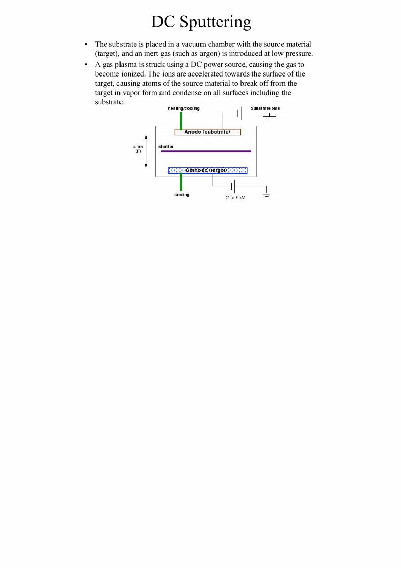
DC Sputtering• The substrate is placed in a vacuum chamber with the source material
(target), and an inert gas (such as argon) is introduced at low pressure.
• A gas plasma is struck using a DC power source, causing the gas to
become ionized. The ions are accelerated towards the surface of the
target, causing atoms of the source material to break off from the
target in vapor form and condense on all surfaces including the
substrate.
8/13/2019 Metallization Lecture
http://slidepdf.com/reader/full/metallization-lecture 18/30
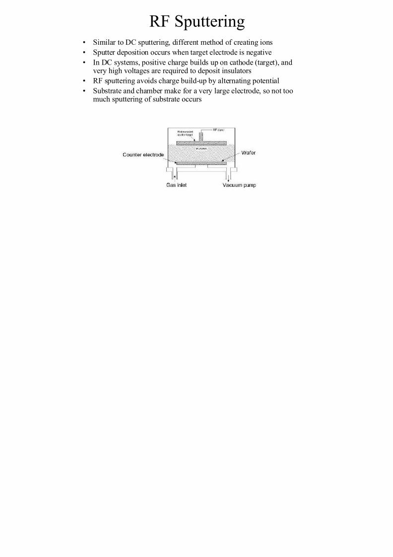
RF Sputtering• Similar to DC sputtering, different method of creating ions
• Sputter deposition occurs when target electrode is negative
• In DC systems, positive charge builds up on cathode (target), andvery high voltages are required to deposit insulators
• RF sputtering avoids charge build-up by alternating potential
• Substrate and chamber make for a very large electrode, so not too
much sputtering of substrate occurs
8/13/2019 Metallization Lecture
http://slidepdf.com/reader/full/metallization-lecture 19/30
Sputtering
• Wafer and target are kept close together to maximize
collection of sputtered material
• Pressure is of the order of 0.1 Torr (mean free path of
the order of 1 mm). This increases step coverage.
• Energy spread of depositing material is of the order of
10-50 eV
• Compromise between increasing the number of Ar ions,
and increasing scattering of Ar ions with neutral Ar
atoms. If you can increase the number of ions without
increasing the number of neutrals, you can operate at
lower pressures
• Particle energy and deposition rate depend strongly on
sputter voltage, substrate bias and pressure
8/13/2019 Metallization Lecture
http://slidepdf.com/reader/full/metallization-lecture 20/30
Sputtering• At frequencies less than 50 kHz, electrons and ions in plasma are
mobile, and both follow the switching of the anode and cathode.This is equivalent to DC sputtering of both surfaces.
• At frequencies above 50 kHz, ions (heavy) can no longer follow theswitching electrons, this neutralizes positive charge build up
• Other variants of sputtering:
– Magnetron sputtering (magnetic and electric field, put magnets behindtarget, higher deposition rate because electrons strike Ar atoms morefrequently)
– Ion deposited sputtering (bombard surface with different ions, requireslow voltage, change in film properties because of local rearrangementof atoms)
– Reactive sputtering (add reactive gas such as oxygen or nitrogen tochamber during deposition, good stoichiometry control, can poisontarget if chemical reaction rate is faster than sputter rate)
• Sputtering compared to evaporation – smaller grain size, manygrain orientations, better adhesion of film

8/13/2019 Metallization Lecture
http://slidepdf.com/reader/full/metallization-lecture 21/30
Casting
• Material is dissolved in liquid form in solvent, and
applied to substrate by spraying or spinning.
• Used for polymers (photoresist) using the spin-coating
method, also used for spin-on glasses.
• Thickness of film ranges from single monolayer (for
adhesion promotion) to tens of microns.
8/13/2019 Metallization Lecture
http://slidepdf.com/reader/full/metallization-lecture 22/30
Chemical Vapor Deposition
• Substrate placed in chamber and number of gases supplied
• Reaction takes place between the source gases, product is a
solid that condenses on all surfaces in the reaction chamber
• Used for many different materials (SiO2, Si3N4,
polysilicon, tungsten, copper, etc.)
• Can have atmospheric pressure CVD or low pressure CVD(much more common), another variant is plasma enhanced
CVD.
8/13/2019 Metallization Lecture
http://slidepdf.com/reader/full/metallization-lecture 23/30
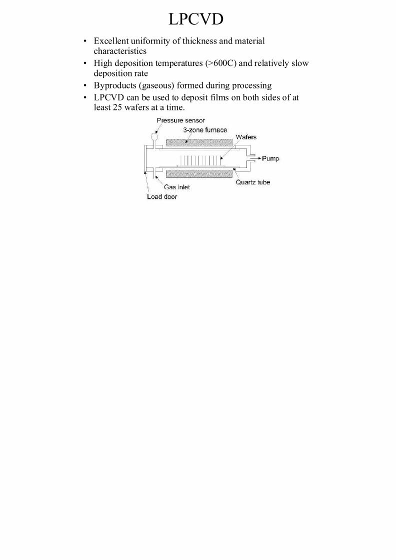
LPCVD• Excellent uniformity of thickness and material
characteristics• High deposition temperatures (>600C) and relatively slow
deposition rate
• Byproducts (gaseous) formed during processing
• LPCVD can be used to deposit films on both sides of atleast 25 wafers at a time.

8/13/2019 Metallization Lecture
http://slidepdf.com/reader/full/metallization-lecture 24/30
PECVD
• Lower temperature process (200-400C)
• Extra energy is supplied to the gas molecules by the
plasma in the reactor
• Quality of films is typically inferior to LPCVD films
• PECVD systems can only deposit films on one side of up
to 4 wafers at a time.
8/13/2019 Metallization Lecture
http://slidepdf.com/reader/full/metallization-lecture 25/30
Electrochemical Deposition• Used for metals such as copper, gold and nickel
• Film thickness can be varied easily (<1micron, >100
microns)
• Control of deposition achieved by using external electric
potential, it requires electrical contact to the substrate
while immersed in a liquid bath
• The surface of the substrate must have an electrically
conducting coating (seed layer) before deposition can be
done using this method
8/13/2019 Metallization Lecture
http://slidepdf.com/reader/full/metallization-lecture 26/30
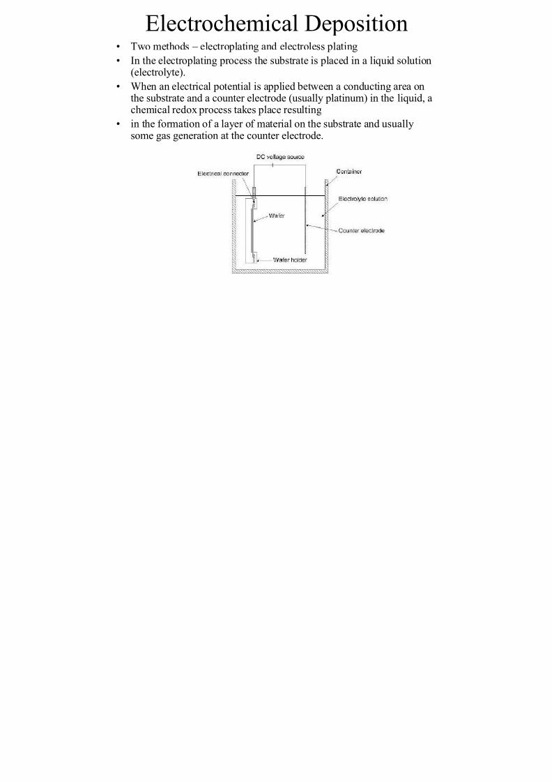
Electrochemical Deposition• Two methods – electroplating and electroless plating
• In the electroplating process the substrate is placed in a liquid solution
(electrolyte).
• When an electrical potential is applied between a conducting area onthe substrate and a counter electrode (usually platinum) in the liquid, achemical redox process takes place resulting
• in the formation of a layer of material on the substrate and usually
some gas generation at the counter electrode.

8/13/2019 Metallization Lecture
http://slidepdf.com/reader/full/metallization-lecture 27/30
Electrochemical Deposition
• In the electroless plating process a more complex chemical
solution is used
• Deposition happens spontaneously on any surface which
forms a sufficiently high electrochemical potential with the
solution.
• It does not require any external electrical potential and
contact to the substrate during processing.
• It is more difficult to control with regards to film thickness
and uniformity.
8/13/2019 Metallization Lecture
http://slidepdf.com/reader/full/metallization-lecture 28/30
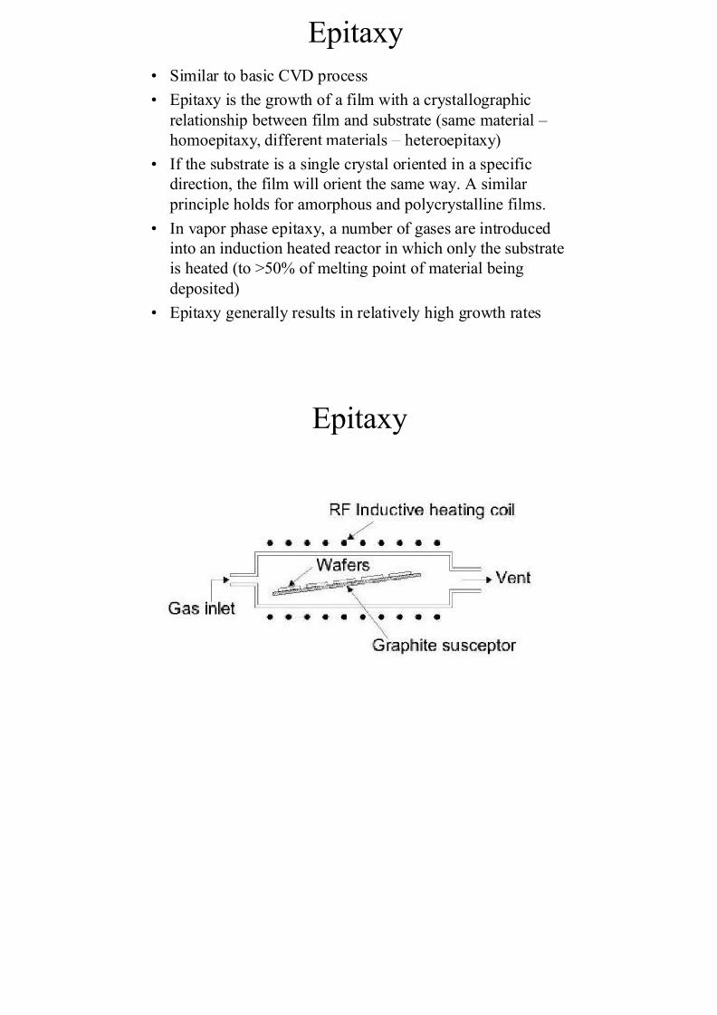
Epitaxy
• Similar to basic CVD process
• Epitaxy is the growth of a film with a crystallographic
relationship between film and substrate (same material –
homoepitaxy, different materials – heteroepitaxy)
• If the substrate is a single crystal oriented in a specific
direction, the film will orient the same way. A similar principle holds for amorphous and polycrystalline films.
• In vapor phase epitaxy, a number of gases are introduced
into an induction heated reactor in which only the substrate
is heated (to >50% of melting point of material beingdeposited)
• Epitaxy generally results in relatively high growth rates

8/13/2019 Metallization Lecture
http://slidepdf.com/reader/full/metallization-lecture 29/30
Epitaxy

8/13/2019 Metallization Lecture
http://slidepdf.com/reader/full/metallization-lecture 30/30
Molecular Beam Epitaxy
• Needs independently controlled thermal and/or electron beam sources for all materials and dopants.
• Evaporation at very low deposition rates
• Typically in ultra-high vacuum
• Very well controlled
• Grow films with good crystal structure
• Expensive
• Often use multiple sources to grow alloy films
• Deposition rate is so low that substrate temperature does
not need to be as high