Embed Size (px)
Citation preview
ACTAUNIVERSITATIS
UPSALIENSISUPPSALA
2016
Digital Comprehensive Summaries of Uppsala Dissertationsfrom the Faculty of Science and Technology 1406
Copper and Silver Metallization forHigh Temperature Applications
SHABNAM MARDANI
ISSN 1651-6214ISBN 978-91-554-9656-2urn:nbn:se:uu:diva-300796
Dissertation presented at Uppsala University to be publicly examined in Polhemsalen,Ångströmlaboratoriet, Lägerhyddsvägen 1, Uppsala, Friday, 30 September 2016 at 09:30 forthe degree of Doctor of Philosophy. The examination will be conducted in English. Facultyexaminer: Prof. Christophe Detavernier Detavernier (Ghent University, Faculty of Sciences,Department of Solid state sciences).
AbstractMardani, S. 2016. Copper and Silver Metallization for High Temperature Applications.Digital Comprehensive Summaries of Uppsala Dissertations from the Faculty of Science andTechnology 1406. 68 pp. Uppsala: Acta Universitatis Upsaliensis. ISBN 978-91-554-9656-2.
High-temperature electrical- and morphological-stability of interconnect is critical for electronicsystems based on wide band gap (WBG) semiconductors. In this context, the thermal stabilityof both Ag and Cu films with Ta and TaN films as diffusion barriers and/or surface-cappinglayers at high temperatures up to 800 oC is investigated in this thesis.
The investigation of un-capped Ag films with either Ta or TaN diffusion barrier layers showselectrical stability upon annealing up to 600 °C. Degradation occurs above 600 °C mainly as aresult of void formation and Ag agglomeration. Sandwiching Ag films between Ta and/or TaNlayers is found to electrically and morphologically stabilize the Ag metallization up to 800 °C.The barrier layer plays a key role; the β-to-α phase transition in the underlying Ta barrier layeris identified as the major cause for the morphological instability of the film above 600 °C. Thisphase transition can be avoided using a stacked Ta/TaN barrier. Furthermore, no observable Tadiffusion in Ag films is found.
Copper films with a Ta diffusion barrier show clearly different behaviors. In the Cu/Tasample, Ta starts to diffuse up to the surface via fast-diffusing grain boundaries (GBs) afterannealing at 500 °C. The activation energy for the GB diffusion is 1.0+0.3 eV. Un-capped Cuis electrically stable up to 800 °C. An appreciable increase in sheet resistance occurs above 600°C for the asymmetric combinations Ta/Cu/TaN and TaN/Cu/Ta. This degradation is closelyrelated to a substantial diffusion of Ta across the Cu film and on to the TaN layer, where Ta1+xNforms. The symmetrical combinations Ta/Cu/Ta and TaN/Cu/TaN show only small changes insheet resistance even after annealing at 800 °C. No Ta diffusion can be found in the Ta/Cu/Taand TaN/Cu/TaN stacks.
Finally, the influence of barrier and cap, their interfaces to Cu and Ta diffusion andsegregation in the Cu GBs on electromigration is studied. Our preliminary results with the TaN/Cu/Ta and TaN/Cu/TaN structures report a 2-fold higher activation energy and a 10-fold longerlifetime for the former, thus confirming an important role of the interface between Cu and thecap and/or barrier.
Keywords: Metallization, Copper, Silver, Tantalum, High tempreture, Diffussion,Electromigration, Stability
Shabnam Mardani, Department of Engineering Sciences, Solid State Electronics, Box 534,Uppsala University, SE-75121 Uppsala, Sweden.
© Shabnam Mardani 2016
ISSN 1651-6214ISBN 978-91-554-9656-2urn:nbn:se:uu:diva-300796 (http://urn.kb.se/resolve?urn=urn:nbn:se:uu:diva-300796)

3
به پدر و مادرم

4
5
List of Papers
This thesis is based on the following papers, which are referred to in the text by their Roman numerals.
I Mardani, S., Primetzhofer, D., Liljeholm, L., Vallin, Ö., Nor-
ström, H., Olsson, J. (2013) Electrical properties of Ag/Ta and Ag/TaN thin-films. Microelectronic Engineering, 120(2014):257–261
II Mardani, S., Vallin, Ö., Wätjen, J., Norström, H., Olsson, J., Zhang, S-L. (2014) Morphological instability of Ag films caused by phase transition in the underlying Ta barrier layer. Applied Physics Letters, 105(2014):071604
III Mardani, S., Norström, H., Smith, U., Olsson, J., Zhang, S-L. (2015) Influence of tantalum/tantalum nitride barriers and caps on the high-temperature properties of copper metallization for wide-band gap applications. Microelectronic Engineering, 137(2015):37–42
IV Mardani, S., Norström, H., Smith, U., Zhang, S-L. (2016) High-temperature Ta diffusion in the grain boundary of thin Cu films. Journal of Vacuum Science & Technology B, 34(2016): 040606
V Mardani, S., Norström, H., Gustavsson, F., Nyberg, T., Pri-
metzhofer, D., Leifer, K., Wu, D., Zhang, S-L. (2016) On Ta diffusion in thin Cu and Ag films. Journal of Vacuum Science & Technology B, Submitted.
VI Mardani, S., Norström, H., Smith, U., Gustavsson, F., Olsson, J., Zhang, S-L. (2016) Electromigration behavior of Cu metalli-zation interfacing with Ta versus TaN at high temperatures. Journal of Vacuum Science & Technology B, Submitted.
Reprints were made with permission from the respective publishers.
6
Author’s contributions
I Minor part of planning, most of the experimental, most of the analysis and part of the writing.
II Major part of planning, all the experimental, all of the analysis and part of the writing.
III Major part of planning, all the experimental, all of the analysis and part of the writing.
IV Major part of planning, all the experimental, all of the analysis and major part of the writing.
V Major part of planning, all the experimental, most of the analy-
sis and minor part of the writing.
VI Major part of planning, all the experimental, most of the analy-sis and minor part of the writing.
7
Related Work
The following paper is related to the work in the thesis but has not been included.
Zetterling, C-M., Hallén, A., Hedayati, R., Kargarrazi, S., Lan-ni, L., Malm, G., Mardani, S., Norström, H., Rusu, A., Su-vanam, S., Tian, Y., Östling, M. (2016) Prospects of Bipolar in-tegrated circuits in SiC for extreme environment operation, Submitted.

8
9
Contents
1. Introduction ............................................................................................... 13
2. The technology.......................................................................................... 17 2.1. SiC characteristics ............................................................................. 17 2.2. Interconnects ..................................................................................... 18 2.3. Barriers .............................................................................................. 19 2.4. Electromigration fundamentals ......................................................... 20
3. Thin film deposition and characterization ................................................ 23 3.1. Thin film deposition .......................................................................... 23 3.2. Annealing .......................................................................................... 25 3.3. Characterization methods .................................................................. 26
3.3.1. Scanning Electron Microscopy (SEM) ...................................... 26 3.3.2. Transmission Electron Microscopy (TEM) ............................... 27 3.3.3. Rutherford Backscattering Spectrometry (RBS) ....................... 28 3.3.4. Time-of-Flight Elastic Recoil Detection (ToF-ERDA) ............. 29 3.3.5. Four point probe measurement .................................................. 30
4. Material study ........................................................................................... 31 4.1. Silver ................................................................................................. 31 4.2. Copper ............................................................................................... 35 4.3. Cu/Ag ................................................................................................ 42
5. Electromigration study .............................................................................. 45 5.1. Test structure ..................................................................................... 45 5.2. Electrical characterization ................................................................. 48
6. Summary ................................................................................................... 53
7. Svensk sammanfattning ............................................................................ 55
Acknowledgments......................................................................................... 59
References ..................................................................................................... 61
10
List of abbreviations
WBG Wide band gap SOI Silicon-on-insulator RC Resistance capacitance SOI Silicon-on-insulator RC Resistance capacitance MTTF Mean time to failure CVD Chemical vapor deposition ALD Atomic layer deposition SEM Scanning Electron Microscopy EDS Energy Dispersive X-ray Spectroscopy FIB Focused Ion Beam TEM Transmission electron microscopy STEM Electron transmission microscopy RBS Rutherford backscattering spectrometry ToF-ERDA Time-of-flight elastic recoil detection XPS X-ray photoelectron spectroscopy GB Grain boundary PECVD Plasma-enhanced chemical vapor deposition PVD Physical vapor deposition EM Electromigration RT Room temperature TTF Time to failure
11
List of symbols
Nc Effective electron density of states Nv Effective hole density of states Eg Bandgap T Temperature ni Intrinsic charge carriers kB Boltzmann constant Tm Melting temperature J Current density Ea Activation energy ts Set-point time TS Set-point temperature V Voltage I Current t Thickness cs Surface concentration Deff Effective diffusion coefficient δ Grain boundary thickness Rs Sheet resistance ΔW Width deviation R0 Initial resistance α Temperature coefficient

12
13
1. Introduction
Electronic devices based on wide band gap (WBG) semiconductors, espe-cially silicon carbide (SiC) and gallium nitride (GaN), have been developed and optimized towards reliable operation at very high temperatures and un-der harsh environmental conditions. Driven by the continuously increasing demands for high-temperature electronics in fields such as energy produc-tion, aeronautics, and aerospace, the WBG devices are steadily becoming more heat tolerant [1-9]. Combined, SiC and GaN device sales are projected to have an exponential growth from today’s (2016) less than $1B industry to a ~$8B industry by 2023 [10]. Up to now, research focus has mainly been on process technology and materials science related to the WBGs [11-14].
The potential of present WBG devices is however limited by the metal-lurgical stability of the on-chip metallization [4, 15-17]. Although urgently needed, there are a number of applications where not even current WBG technology can provide satisfactory solutions, such as power converters for aircraft, actuators for high voltage systems, power-modules for hybrid elec-trical vehicles, devices for space exploration and devices for deep oil/gas extraction [16]. Without a well characterized and fully functional metalliza-tion concept, suitable for very high operating temperatures, the inherent po-tential of the WBG devices cannot be fully utilized.
In this thesis, various experiments have been performed to explore solu-tions to overcome the above-mentioned metallization limitations so that the WBG devices could work at very high temperatures, i.e. at least up to 500 °C.
Currently, commercial silicon-on-insulator (SOI) devices are dominant in the field of low-power, high-temperature applications up to 300 °C [9]. However, practical operation of Si devices at ambient temperatures above 200 °C appears to be problematic due to electrical leakage and self-heating, both can lead to severe performance and reliability degradation.
Consequently, a solution for electronic systems that simultaneously re-quire high-temperature and high-power operation is to use WBGs. The im-portant advantage of WBGs in these operating conditions is probably their low or moderate intrinsic carrier concentrations at those high operation tem-peratures, since they are orders of magnitude lower than that of Si. Every semiconductor has a certain concentration of electrons and holes which is temperature dependent. The concentration of these intrinsic charge carriers (ni in cm3) are exponentially temperature dependent, as expressed in eq 1.
14
/ eq.1
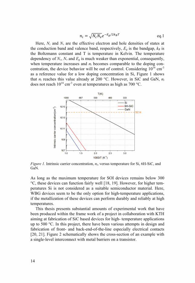
Here, Nc and Nv are the effective electron and hole densities of states at the conduction band and valence band, respectively, Eg is the bandgap, kB is the Boltzmann constant and T is temperature in Kelvin. The temperature dependency of Nc, Nv and Eg is much weaker than exponential, consequently, when temperature increases and ni becomes comparable to the doping con-centration, the device behavior will be out of control. Considering 1014 cm-3 as a reference value for a low doping concentration in Si, Figure 1 shows that ni reaches this value already at 200 °C. However, in SiC and GaN, ni does not reach 1014 cm-3 even at temperatures as high as 700 °C.
Figure 1. Intrinsic carrier concentration, ni, versus temperature for Si, 6H-SiC, and GaN.
As long as the maximum temperature for SOI devices remains below 300 °C, these devices can function fairly well [18, 19]. However, for higher tem-peratures Si is not considered as a suitable semiconductor material. Here, WBG devices seem to be the only option for high-temperature applications, if the metallization of these devices can perform durably and reliably at high temperatures.
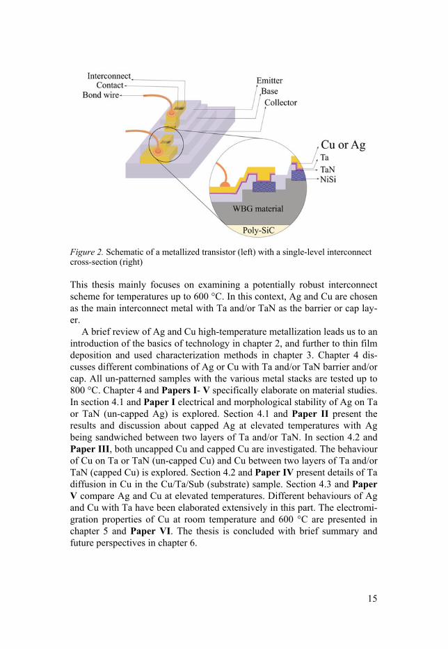
This thesis presents substantial amounts of experimental work that have been produced within the frame work of a project in collaboration with KTH aiming at fabrication of SiC based devices for high- temperature applications up to 500 °C. In this project, there have been various attempts in design and fabrication of front- and back-end-of-the-line especially electrical contacts [20, 21]. Figure 2 schematically shows the cross-section of an example with a single-level interconnect with metal barriers on a transistor.
15
Figure 2. Schematic of a metallized transistor (left) with a single-level interconnect cross-section (right)
This thesis mainly focuses on examining a potentially robust interconnect scheme for temperatures up to 600 °C. In this context, Ag and Cu are chosen as the main interconnect metal with Ta and/or TaN as the barrier or cap lay-er.
A brief review of Ag and Cu high-temperature metallization leads us to an introduction of the basics of technology in chapter 2, and further to thin film deposition and used characterization methods in chapter 3. Chapter 4 dis-cusses different combinations of Ag or Cu with Ta and/or TaN barrier and/or cap. All un-patterned samples with the various metal stacks are tested up to 800 °C. Chapter 4 and Papers I- V specifically elaborate on material studies. In section 4.1 and Paper I electrical and morphological stability of Ag on Ta or TaN (un-capped Ag) is explored. Section 4.1 and Paper II present the results and discussion about capped Ag at elevated temperatures with Ag being sandwiched between two layers of Ta and/or TaN. In section 4.2 and Paper III, both uncapped Cu and capped Cu are investigated. The behaviour of Cu on Ta or TaN (un-capped Cu) and Cu between two layers of Ta and/or TaN (capped Cu) is explored. Section 4.2 and Paper IV present details of Ta diffusion in Cu in the Cu/Ta/Sub (substrate) sample. Section 4.3 and Paper V compare Ag and Cu at elevated temperatures. Different behaviours of Ag and Cu with Ta have been elaborated extensively in this part. The electromi-gration properties of Cu at room temperature and 600 °C are presented in chapter 5 and Paper VI. The thesis is concluded with brief summary and future perspectives in chapter 6.

16
17
2. The technology
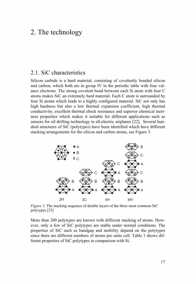
2.1. SiC characteristics Silicon carbide is a hard material, consisting of covalently bonded silicon and carbon, which both are in group IV in the periodic table with four val-ance electrons. The strong covalent bond between each Si atom with four C atoms makes SiC an extremely hard material. Each C atom is surrounded by four Si atoms which leads to a highly configured material. SiC not only has high hardness but also a low thermal expansion coefficient, high thermal conductivity, excellent thermal shock resistance and superior chemical inert-ness properties which makes it suitable for different applications such as sensors for oil drilling technology to all-electric airplanes [22]. Several hun-dred structures of SiC (polytypes) have been identified which have different stacking arrangements for the silicon and carbon atoms, see Figure 3.
Figure 3. The stacking sequence of double layers of the three most common SiC polytypes [23]
More than 200 polytypes are known with different stacking of atoms. How-ever, only a few of SiC polytypes are stable under normal conditions. The properties of SiC such as bandgap and mobility depend on the polytypes since there are different numbers of atoms per unite cell. Table 1 shows dif-ferent properties of SiC polytypes in comparison with Si.
18
Table 1. Material properties of Si and SiC
Unit Si 3C-SiC 6H-SiC 4H-SiC
Eg eV 1.12 2.4 3 3.2 Lattice a Å 5.43 4.36 3.08 3.08 Lattice c Å - - 15.12 10.08 Density g/cm3 2.3 3.2 3.2 3.2 Thermal Conductivity
W/cmK 1.5 5 5 5
Melting point °C 1420 2830 2830 2830
2.2. Interconnects In this thesis two different metals, Cu and Ag, are investigated to assess to what extent these metals can be adopted for high-temperature applications.
Copper is a technologically mature conductor material for interconnects in advanced integrated silicon circuits due to its high conductivity, good high frequency performance [24], and excellent resistance to electromigration [25-31]. Due to its superior electrical and electromigration resistance com-pared to aluminum alloys, the resistance capacitance (RC) delay times de-creases and failure due to electromigration reduces in Cu interconnects [32, 33]. However, Cu technology is concerned about issues such as compat-ibility in fabrication process and high diffusivity in Si [34, 35]. Hence, liners or barrier films are mandatory to prevent potential diffusion into surrounding dielectrics and into active Si [31].
On the other hand, Ag has the lowest resistivity (1.59 μΩ.cm in bulk re-sistivity at 20 °C) of all metals, and it has a high oxidation resistance in comparison with Al and Cu. Ag has better electromigration resistance than Al [36]. It has also been reported that the electromigration resistance gets enhanced by coating Ag with Cr and TiO2 [36, 37]. These properties of Ag make it as promising candidate to be considered as possible interconnect material.
Table 2. Comparison of properties of Ag , Cu and Al
Properties unit Ag Cu Al
Bulk resistivity µΩ.cm 1.59 1.68 2.65 Thin film resistivity µΩ.cm 2.0 (Ag/Ti) 2.8 (Cu/Ni) 3.3 (Al-Cu) Melting point °C 961 1298 706 Mean free path of electron nm 52 39 15 Thermal conductivity Wcm-1K-1 4.25 3.98 2.38 TCR×10-3 K-1 4.1 4.3 4
19
However, Ag suffers from poor adhesion on SiO2, hence adhesion pro-moters are needed. Moreover, passivation layers to protect it against corro-sive environments like the presence of sulfur is essential in order to define the proper interconnection wiring [37]. Table 2 shows different electrical, physical and thermal properties of Cu, Ag and Al.
2.3. Barriers As it was mentioned earlier for using Ag and Cu as interconnects, diffusion barriers are needed to prevent degradation of devices as a result of poor ad-hesion and diffusion. The metallurgical stability of a diffusion barrier with respect to the metal that carries the current should be considered for the choice of a diffusion barrier [38]. According to the empirical rule, the acti-vation energy for the particular diffusion process is proportional to the melt-ing temperature Tm of materials. Therefore an efficient diffusion barrier should have a high melting point. Hence, refractory metals with Tm >2000 °C are proper candidates for Cu and consequently for Ag [31]. Different refractory metals such as Ti [39], W [40] and Ta [41] have been investigated extensively. Moreover, refractory metal nitrides such as polycrystalline and amorphous TiNx [42], TaNx [43], and WNx [44] are widely recognized as attractive diffusion barriers and generally characterized by a low electrical resistivity and thermodynamic stability [31].
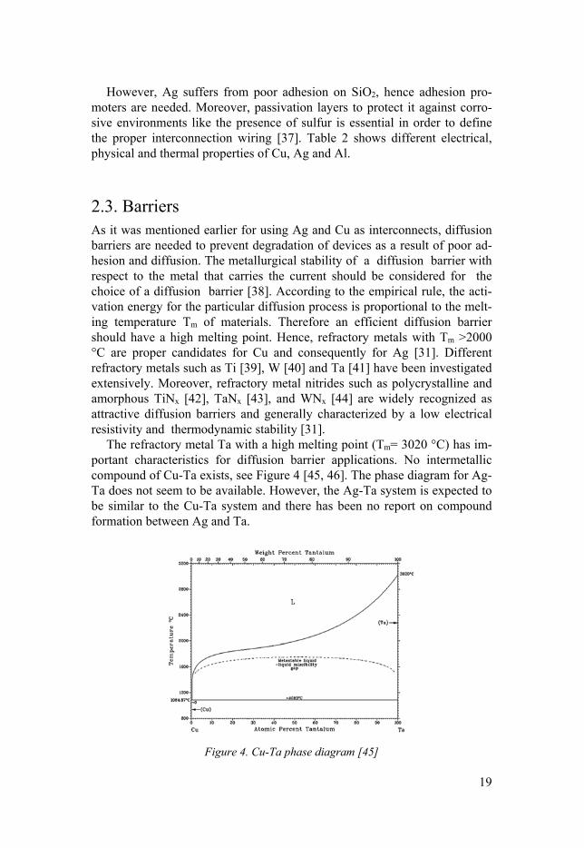
The refractory metal Ta with a high melting point (Tm= 3020 °C) has im-portant characteristics for diffusion barrier applications. No intermetallic compound of Cu-Ta exists, see Figure 4 [45, 46]. The phase diagram for Ag-Ta does not seem to be available. However, the Ag-Ta system is expected to be similar to the Cu-Ta system and there has been no report on compound formation between Ag and Ta.
Figure 4. Cu-Ta phase diagram [45]
20
Moreover, the solid solubility between Cu and Ta and vice versa is very small [45]. Therefore, Ta-based barriers are of particular interest due to po-tentially good barrier properties [47-49]. However, the adhesion of Ta to SiO2 is not that good in comparison with TaN to SiO2 [50, 51]. Considering good adhesion between metallization materials Ta shows strong adhesion to Cu [52]. The combination of metal stack Ta/TaNx is an established barrier layer in the Cu interconnect and it has been explored extensively [53-55].
A lot of works have focused on three different Ta modifications: (i) thermodynamically metastable tetragonal β-Ta (ii) thermodynamically stable body-centered cubic (bcc) α-Ta and (iii) amorphous Ta. Table 3 shows dif-ferent properties of these three Ta phases.
Table 3. Summary of different properties for different Ta modifications [31, 56, 57]
Unit α-Ta β-Ta Amorphous Ta
Lattice a Å 5.43 10.21 - Lattice c Å - 5.31 - Resistivity µΩ.cm 15-50 150-220 150-180 Thermal expanion coeficient
°C-1 6.9×10⁻⁶ 6×10⁻⁶ -
Depending on deposition method and deposition parameters one or a mixture of these phases can be formed in Ta layer. Deposition of Ta on Si and SiO2 at room temperature usually results in β-Ta [48, 51, 58]. By depositing Ta on Si and SiO2 at temperatures above 400 °C α-Ta will be formed [59]. Meta-stable β-Ta to stable α-Ta transformation occurs during thermal treatment in the temperature range of 600 °C to 800 °C [53, 60-62]. This transformation temperature depends on the Ta layer thickness according to Hogeveen et al.[63] . Moreover, the α-Ta can be formed by depositing Ta onto TaN [64, 65]. The stable α-Ta has lower electrical resistivity according to Ta/TaNx established barrier layer [53, 54].
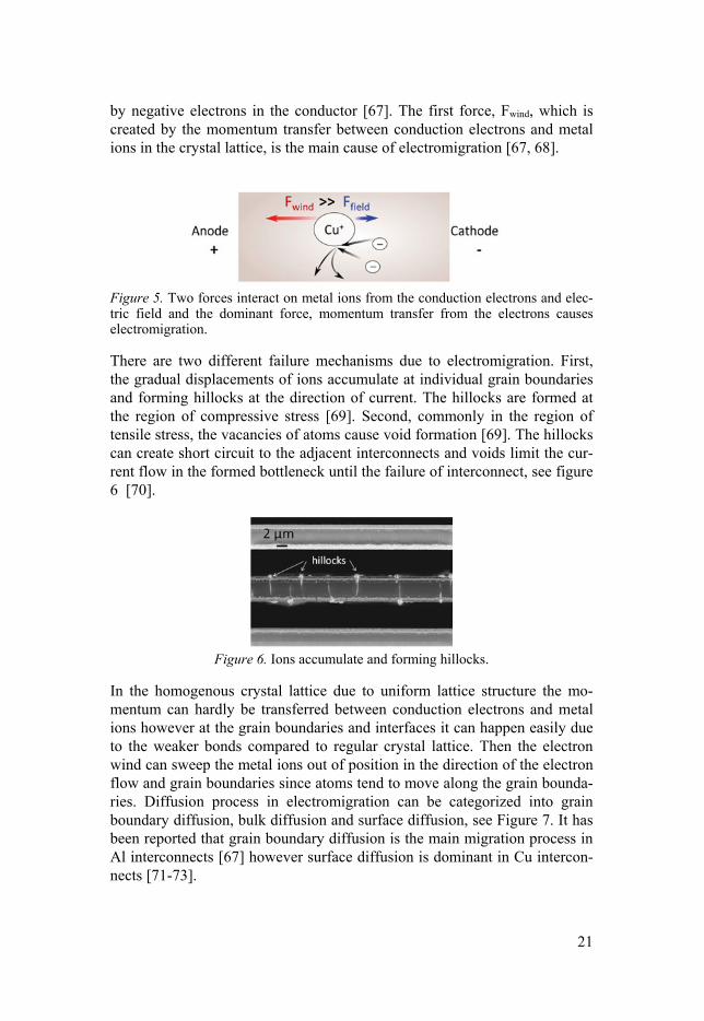
2.4. Electromigration fundamentals Electromigration is an indication of mass transportation in the metal when it is under stress because of high current density. This phenomenon has been known for several decades [66]. Figure 5 shows the basic process as a result of electromigration. As the current flows through the interconnect there is an interaction between the moving electrons (electron wind) and the metal ions. It occurs when the current density is high enough to drift the metal ions in the direction of electron flow. This force is shown by Fwind in Figure 5. On the other hand, there is an electrostatic force Ffield caused by electric field in interconnect. This force can be neglected since the positive ions are shielded
21
by negative electrons in the conductor [67]. The first force, Fwind, which is created by the momentum transfer between conduction electrons and metal ions in the crystal lattice, is the main cause of electromigration [67, 68].
Figure 5. Two forces interact on metal ions from the conduction electrons and elec-tric field and the dominant force, momentum transfer from the electrons causes electromigration.
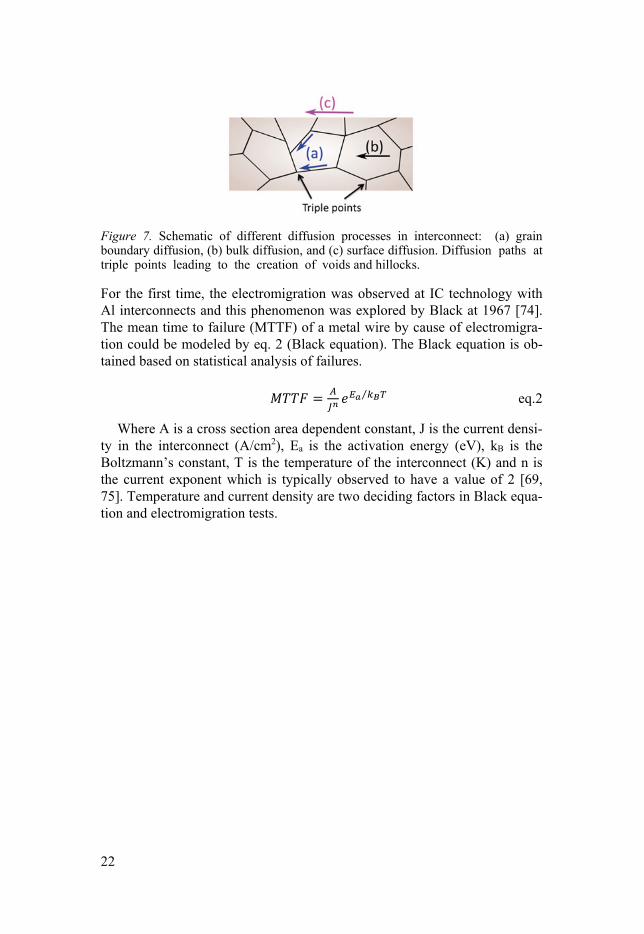
There are two different failure mechanisms due to electromigration. First, the gradual displacements of ions accumulate at individual grain boundaries and forming hillocks at the direction of current. The hillocks are formed at the region of compressive stress [69]. Second, commonly in the region of tensile stress, the vacancies of atoms cause void formation [69]. The hillocks can create short circuit to the adjacent interconnects and voids limit the cur-rent flow in the formed bottleneck until the failure of interconnect, see figure 6 [70].
Figure 6. Ions accumulate and forming hillocks.
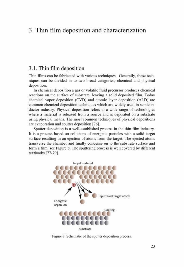
In the homogenous crystal lattice due to uniform lattice structure the mo-mentum can hardly be transferred between conduction electrons and metal ions however at the grain boundaries and interfaces it can happen easily due to the weaker bonds compared to regular crystal lattice. Then the electron wind can sweep the metal ions out of position in the direction of the electron flow and grain boundaries since atoms tend to move along the grain bounda-ries. Diffusion process in electromigration can be categorized into grain boundary diffusion, bulk diffusion and surface diffusion, see Figure 7. It has been reported that grain boundary diffusion is the main migration process in Al interconnects [67] however surface diffusion is dominant in Cu intercon-nects [71-73].
22
Figure 7. Schematic of different diffusion processes in interconnect: (a) grain boundary diffusion, (b) bulk diffusion, and (c) surface diffusion. Diffusion paths at triple points leading to the creation of voids and hillocks.
For the first time, the electromigration was observed at IC technology with Al interconnects and this phenomenon was explored by Black at 1967 [74]. The mean time to failure (MTTF) of a metal wire by cause of electromigra-tion could be modeled by eq. 2 (Black equation). The Black equation is ob-tained based on statistical analysis of failures.
⁄ eq.2
Where A is a cross section area dependent constant, J is the current densi-ty in the interconnect (A/cm2), Ea is the activation energy (eV), kB is the Boltzmann’s constant, T is the temperature of the interconnect (K) and n is the current exponent which is typically observed to have a value of 2 [69, 75]. Temperature and current density are two deciding factors in Black equa-tion and electromigration tests.
23
3. Thin film deposition and characterization
3.1. Thin film deposition Thin films can be fabricated with various techniques. Generally, these tech-niques can be divided in to two broad categories; chemical and physical deposition.
In chemical deposition a gas or volatile fluid precursor produces chemical reactions on the surface of substrate, leaving a solid deposited film. Today chemical vapor deposition (CVD) and atomic layer deposition (ALD) are common chemical deposition techniques which are widely used in semicon-ductor industry. Physical deposition refers to a wide range of technologies where a material is released from a source and is deposited on a substrate using physical means. The most common techniques of physical depositions are evaporation and sputter deposition [76].
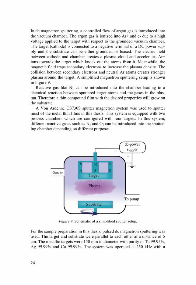
Sputter deposition is a well-established process in the thin film industry. It is a process based on collisions of energetic particles with a solid target surface resulting in an ejection of atoms from the target. The ejected atoms transverse the chamber and finally condense on to the substrate surface and form a film, see Figure 8. The sputtering process is well covered by different textbooks [77-79].
Figure 8. Schematic of the sputter deposition process.
24
In dc magnetron sputtering, a controlled flow of argon gas is introduced into the vacuum chamber. The argon gas is ionized into Ar+ and e- due to a high voltage applied to the target with respect to the grounded vacuum chamber. The target (cathode) is connected to a negative terminal of a DC power sup-ply and the substrate can be either grounded or biased. The electric field between cathode and chamber creates a plasma cloud and accelerates Ar+ ions towards the target which knock out the atoms from it. Meanwhile, the magnetic field traps secondary electrons to increase the plasma density. The collision between secondary electrons and neutral Ar atoms creates stronger plasma around the target. A simplified magnetron sputtering setup is shown in Figure 9.
Reactive gas like N2 can be introduced into the chamber leading to a chemical reaction between sputtered target atoms and the gases in the plas-ma. Therefore a thin compound film with the desired properties will grow on the substrate.
A Von Ardenne CS730S sputter magnetron system was used to sputter most of the metal thin films in this thesis. This system is equipped with two process chambers which are configured with four targets. In this system, different reactive gases such as N2 and O2 can be introduced into the sputter-ing chamber depending on different purposes.
Figure 9. Schematic of a simplified sputter setup.
For the sample preparation in this thesis, pulsed dc magnetron sputtering was used. The target and substrate were parallel to each other at a distance of 5 cm. The metallic targets were 150 mm in diameter with purity of Ta 99.95%, Ag 99.99% and Cu 99.99%. The system was operated at 250 kHz with a
25
90% duty cycle and the base pressure was below 10-4 Pa. Detailed parame-ters for sample depositions are summarized in Table 4.
Table 4. Different material deposition parameters
Power (W) Deposition rate (nm/min) N2/Ar flow ratio Pressure (Pa)
Ag 200 222 - 6×10⁻³ Cu 200 99.6 - 6×10⁻³ Ta 300 69.5 - 6×10⁻³ TaN 500 59.7 0.28 6×10⁻³
As a starting point for depositing TaN films, two different N2/Ar flow ratios, 0.16 and 0.28, were selected. Both TaN films with different N2 concentra-tions showed the same behaviour, hence the 0.28 N2/Ar flow ratio which had almost stoichiometric composition (Paper II), was chosen for all experi-ments.
The samples discussed in Paper I were prepared in a Lesker sputter mag-netron system. The metallic targets were 5 cm in diameter and the target substrate separation was 18 cm at an oblique angle of 16°.
In all experiments the substrates were un-patterned Si wafers with 550 nm thick SiO2 layer grown by thermal oxidation after standard wafer cleaning (RCA1 and RCA2) [80]. Moreover, some samples on diamond foils pre-pared by chemical vapor deposition were also used as substrates in order to determine the composition of sputtered films, specifically TaN films, (Paper II).
3.2. Annealing After deposition, the wafers were cut into rectangular samples, each with an area of 2 cm2 for annealing and further characterizations. The setup used for annealing the samples was a vacuum quartz tube with elliptical radiant heat-ing chamber shown in Figure 10a. Two sample carriers were used in the tube for placing the samples. The pressure in the tube was below 1.3×10⁻⁵ Pa. The tube and carriers were kept under vacuum during standby to minimize sur-face moisture absorption and decrease the risk of oxidation of the metal layer samples during the annealing. After loading, the tube was evacuated by a turbo-molecular pump and the furnace was ramped from room-temperature to the desired temperature set-point in 60 minutes. Depending on the desired annealing time (ts) the samples were kept in the set-point temperature (TS) and the cooldown was performed by stopping the heating source. No extra cooling was used during the cooldown phase, see Figure 10b.
26
Figure 10. (a) Annealing setup with vacuum quartz tube with elliptical radiant heat-ing chamber, (b) annealing temperature and time relations
3.3. Characterization methods Different techniques were used for analyzing the as-deposited films and after each annealing temperature. The most commonly used techniques are briefly explained in this section.
3.3.1. Scanning Electron Microscopy (SEM) The morphology and cross section of metallic films were characterized by SEM using a Zeiss Leo 1550 and Zeiss Merlin. Both tools are equipped with an OXFORD Energy Dispersive X-ray Spectroscopy (EDS) system for ele-mental analysis. The acceleration voltage used for samples in this thesis dif-fered from 5 to 20 kV. The operation principle of a SEM is to focus a beam of electrons using electromagnetic lenses to a spot and scanning from spot to spot over the sample. The electrons interact with atoms in the sample, pro-
27
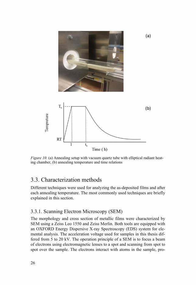
ducing various signals that contain information about the surface topography and composition of the sample. For cross-section characterization, samples were prepared using a FEI Strata DB235 Focused Ion Beam (FIB). Figure 11 shows an example of preparation of the cross section by FIB and SEM cross section.
Figure 11.(a) Preparation of the cross section by FIB and (b) the SEM cross section of a TaN/Ag/Ta/Sub sample after annealing at 800 °C.
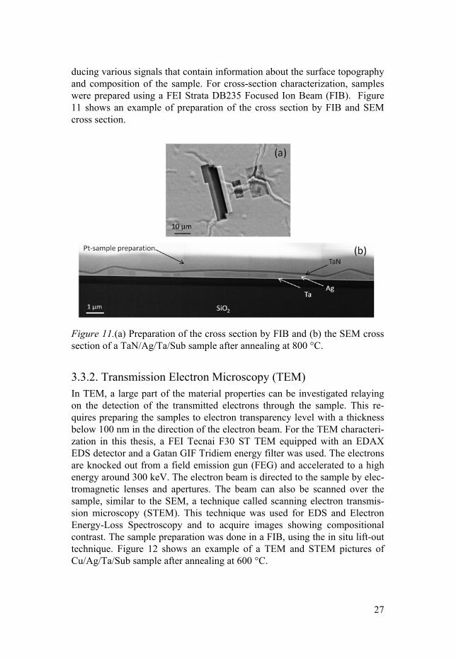
3.3.2. Transmission Electron Microscopy (TEM) In TEM, a large part of the material properties can be investigated relaying on the detection of the transmitted electrons through the sample. This re-quires preparing the samples to electron transparency level with a thickness below 100 nm in the direction of the electron beam. For the TEM characteri-zation in this thesis, a FEI Tecnai F30 ST TEM equipped with an EDAX EDS detector and a Gatan GIF Tridiem energy filter was used. The electrons are knocked out from a field emission gun (FEG) and accelerated to a high energy around 300 keV. The electron beam is directed to the sample by elec-tromagnetic lenses and apertures. The beam can also be scanned over the sample, similar to the SEM, a technique called scanning electron transmis-sion microscopy (STEM). This technique was used for EDS and Electron Energy-Loss Spectroscopy and to acquire images showing compositional contrast. The sample preparation was done in a FIB, using the in situ lift-out technique. Figure 12 shows an example of a TEM and STEM pictures of Cu/Ag/Ta/Sub sample after annealing at 600 °C.
28
Figure 12. (a) TEM and (b) STEM pictures of Cu/Ag/Ta/Sub sample after annealing at 600 °C
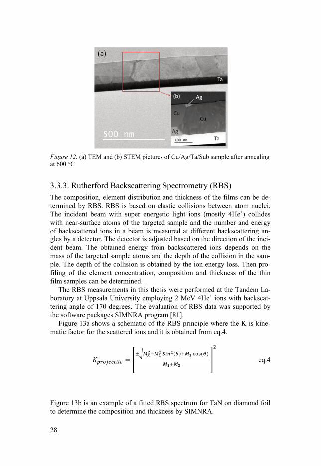
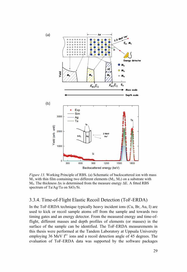
3.3.3. Rutherford Backscattering Spectrometry (RBS) The composition, element distribution and thickness of the films can be de-termined by RBS. RBS is based on elastic collisions between atom nuclei. The incident beam with super energetic light ions (mostly 4He+) collides with near-surface atoms of the targeted sample and the number and energy of backscattered ions in a beam is measured at different backscattering an-gles by a detector. The detector is adjusted based on the direction of the inci-dent beam. The obtained energy from backscattered ions depends on the mass of the targeted sample atoms and the depth of the collision in the sam-ple. The depth of the collision is obtained by the ion energy loss. Then pro-filing of the element concentration, composition and thickness of the thin film samples can be determined.
The RBS measurements in this thesis were performed at the Tandem La-boratory at Uppsala University employing 2 MeV 4He+ ions with backscat-tering angle of 170 degrees. The evaluation of RBS data was supported by the software packages SIMNRA program [81].
Figure 13a shows a schematic of the RBS principle where the K is kine-matic factor for the scattered ions and it is obtained from eq.4.
eq.4
Figure 13b is an example of a fitted RBS spectrum for TaN on diamond foil to determine the composition and thickness by SIMNRA.
29
Figure 13. Working Principle of RBS. (a) Schematic of backscattered ion with mass M1, with thin film containing two different elements (M2, M3) on a substrate with M4. The thickness Δx is determined from the measure energy ΔE. A fitted RBS spectrum of Ta/Ag/Ta on SiO2/Si.
3.3.4. Time-of-Flight Elastic Recoil Detection (ToF-ERDA) In the ToF-ERDA technique typically heavy incident ions (Cu, Br, Au, I) are used to kick or recoil sample atoms off from the sample and towards two timing gates and an energy detector. From the measured energy and time-of-flight, different masses and depth profiles of elements (or masses) in the surface of the sample can be identified. The ToF-ERDA measurements in this thesis were performed at the Tandem Laboratory at Uppsala University employing 36 MeV I8+ ions and a recoil detection angle of 45 degrees. The evaluation of ToF-ERDA data was supported by the software packages
30
CONTES program. Technical about the ToF-ERDA setup can be found in the literature [82] . The main purpose of using ToF-ERDA in this thesis was to determine the nitrogen content of the TaN films since the technique pro-vides simultaneous and quantitative elemental depth distributions for light-mass elements in heavy matrices.
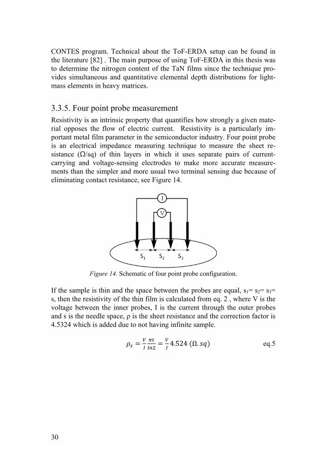
3.3.5. Four point probe measurement Resistivity is an intrinsic property that quantifies how strongly a given mate-rial opposes the flow of electric current. Resistivity is a particularly im-portant metal film parameter in the semiconductor industry. Four point probe is an electrical impedance measuring technique to measure the sheet re-sistance (Ω/sq) of thin layers in which it uses separate pairs of current-carrying and voltage-sensing electrodes to make more accurate measure-ments than the simpler and more usual two terminal sensing due because of eliminating contact resistance, see Figure 14.
Figure 14. Schematic of four point probe configuration.
If the sample is thin and the space between the probes are equal, s1= s2= s3= s, then the resistivity of the thin film is calculated from eq. 2 , where V is the voltage between the inner probes, I is the current through the outer probes and s is the needle space, ρ is the sheet resistance and the correction factor is 4.5324 which is added due to not having infinite sample.
4.524 Ω. eq.5
31
4. Material study
This chapter is an overview of the most important findings on how different Ag and Cu behave at elevated temperatures. The chapter is divided in to three main sections. The first section concerns material characterization and behavior of blank Ag with Ta and/or TaN as a barrier and/or cap, as-deposited and after annealing up to 800 °C. In the second section, material characterization and behavior of blank Cu with Ta and/or TaN as a barrier and/or cap, as-deposited and after annealing up to 800 °C are discussed. The third section elaborates on both Ag and Cu with Ta as a barrier, as-deposited and after annealing up to 600 °C.
4.1. Silver In this thesis and Papers I and II, Ag with Ta and/or TaN as a barrier or cap at elevated temperatures has been studied in a systematic way. Table 5 shows the multilayer structures and their thicknesses for Ag. All the layers were deposited consecutively, without breaking vacuum with the details that were explained in Chapter 3.
Table 5. Fabricated Ag samples
Group Layer Structure Film thickness (nm)
Un-capped Ag Ag/Ta/Sub 100/50/Sub Ag/TaN/Sub 100/50/Sub Capped Ag Ta/Ag/Ta/Sub 50/100/50/Sub TaN/Ag/TaN/Sub 50/100/50/Sub Ta/Ag/TaN/Sub 50/100/50/Sub TaN/Ag/Ta/Sub 50/100/50/Sub
Un-capped Ag is explained in detail in Paper I. The samples in this paper were fabricated by Lesker magnetron sputtering however they were also duplicated with the Von Ardenne sputtering setup to be able to compare the results with all other samples since they were fabricated with the Von Ar-denne sputtering setup. Fabrication parameters and details of these samples are explained in Chapter 3. The wafers were cut to small samples and an-nealed up to 800°C and characterized by four point probe measurement,
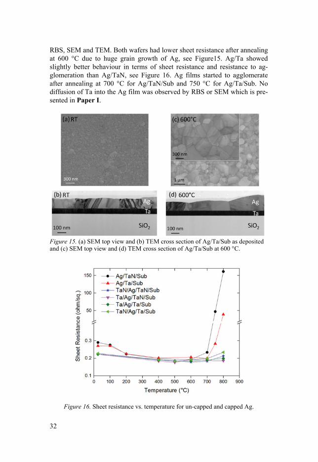
32
RBS, SEM and TEM. Both wafers had lower sheet resistance after annealing at 600 °C due to huge grain growth of Ag, see Figure15. Ag/Ta showed slightly better behaviour in terms of sheet resistance and resistance to ag-glomeration than Ag/TaN, see Figure 16. Ag films started to agglomerate after annealing at 700 °C for Ag/TaN/Sub and 750 °C for Ag/Ta/Sub. No diffusion of Ta into the Ag film was observed by RBS or SEM which is pre-sented in Paper I.
Figure 15. (a) SEM top view and (b) TEM cross section of Ag/Ta/Sub as deposited and (c) SEM top view and (d) TEM cross section of Ag/Ta/Sub at 600 °C.
Figure 16. Sheet resistance vs. temperature for un-capped and capped Ag.
33
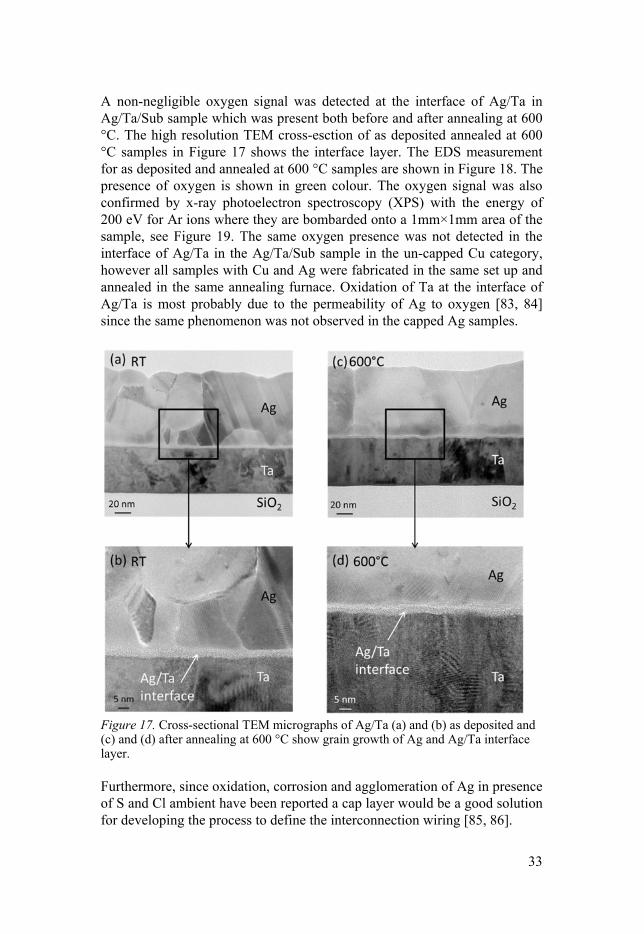
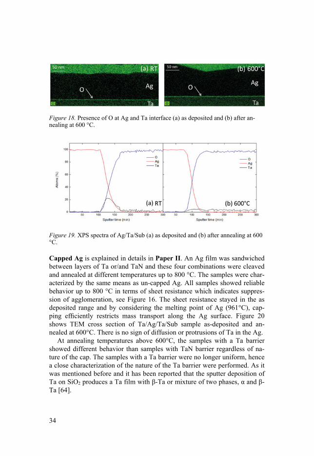
A non-negligible oxygen signal was detected at the interface of Ag/Ta in Ag/Ta/Sub sample which was present both before and after annealing at 600 °C. The high resolution TEM cross-esction of as deposited annealed at 600 °C samples in Figure 17 shows the interface layer. The EDS measurement for as deposited and annealed at 600 °C samples are shown in Figure 18. The presence of oxygen is shown in green colour. The oxygen signal was also confirmed by x-ray photoelectron spectroscopy (XPS) with the energy of 200 eV for Ar ions where they are bombarded onto a 1mm×1mm area of the sample, see Figure 19. The same oxygen presence was not detected in the interface of Ag/Ta in the Ag/Ta/Sub sample in the un-capped Cu category, however all samples with Cu and Ag were fabricated in the same set up and annealed in the same annealing furnace. Oxidation of Ta at the interface of Ag/Ta is most probably due to the permeability of Ag to oxygen [83, 84] since the same phenomenon was not observed in the capped Ag samples.
Figure 17. Cross-sectional TEM micrographs of Ag/Ta (a) and (b) as deposited and (c) and (d) after annealing at 600 °C show grain growth of Ag and Ag/Ta interface layer.
Furthermore, since oxidation, corrosion and agglomeration of Ag in presence of S and Cl ambient have been reported a cap layer would be a good solution for developing the process to define the interconnection wiring [85, 86].
34
Figure 18. Presence of O at Ag and Ta interface (a) as deposited and (b) after an-nealing at 600 °C.
Figure 19. XPS spectra of Ag/Ta/Sub (a) as deposited and (b) after annealing at 600 °C.
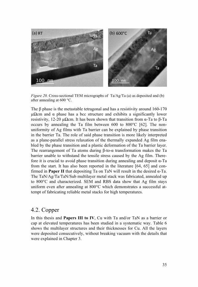
Capped Ag is explained in details in Paper II. An Ag film was sandwiched between layers of Ta or/and TaN and these four combinations were cleaved and annealed at different temperatures up to 800 °C. The samples were char-acterized by the same means as un-capped Ag. All samples showed reliable behavior up to 800 °C in terms of sheet resistance which indicates suppres-sion of agglomeration, see Figure 16. The sheet resistance stayed in the as deposited range and by considering the melting point of Ag (961°C), cap-ping efficiently restricts mass transport along the Ag surface. Figure 20 shows TEM cross section of Ta/Ag/Ta/Sub sample as-deposited and an-nealed at 600°C. There is no sign of diffusion or protrusions of Ta in the Ag.
At annealing temperatures above 600°C, the samples with a Ta barrier showed different behavior than samples with TaN barrier regardless of na-ture of the cap. The samples with a Ta barrier were no longer uniform, hence a close characterization of the nature of the Ta barrier were performed. As it was mentioned before and it has been reported that the sputter deposition of Ta on SiO2 produces a Ta film with β-Ta or mixture of two phases, α and β-Ta [64].
35
Figure 20. Cross-sectional TEM micrographs of Ta/Ag/Ta (a) as deposited and (b) after annealing at 600 °C.
The β phase is the metastable tetragonal and has a resistivity around 160-170 µΩcm and α phase has a bcc structure and exhibits a significantly lower resistivity, 12-20 µΩcm. It has been shown that transition from α-Ta to β-Ta occurs by annealing the Ta film between 600 to 800°C [62]. The non-uniformity of Ag films with Ta barrier can be explained by phase transition in the barrier Ta. The role of said phase transition is more likely interpreted as a plane-parallel stress relaxation of the thermally expanded Ag film ena-bled by the phase transition and a plastic deformation of the Ta barrier layer. The rearrangement of Ta atoms during β-to-α transformation makes the Ta barrier unable to withstand the tensile stress caused by the Ag film. There-fore it is crucial to avoid phase transition during annealing and deposit α-Ta from the start. It has also been reported in the literature [64, 65] and con-firmed in Paper II that depositing Ta on TaN will result in the desired α-Ta. The TaN/Ag/Ta/TaN/Sub multilayer metal stack was fabricated, annealed up to 800°C and characterized. SEM and RBS data show that Ag film stays uniform even after annealing at 800°C which demonstrates a successful at-tempt of fabricating reliable metal stacks for high temperatures.
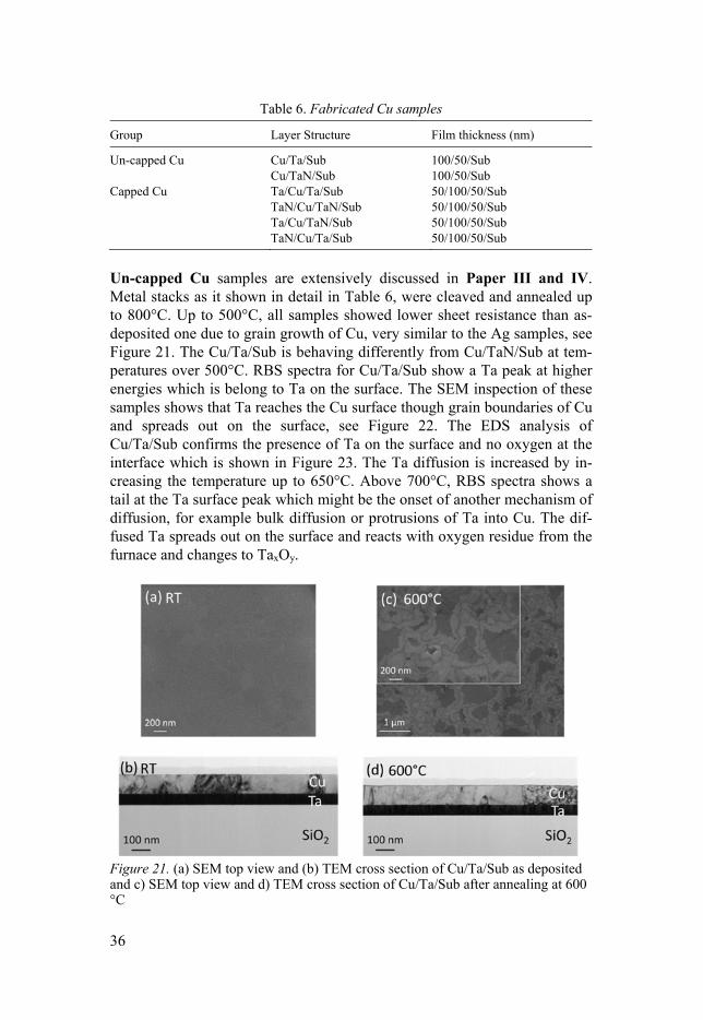
4.2. Copper In this thesis and Papers III to IV, Cu with Ta and/or TaN as a barrier or cap at elevated temperatures has been studied in a systematic way. Table 6 shows the multilayer structures and their thicknesses for Cu. All the layers were deposited consecutively, without breaking vacuum with the details that were explained in Chapter 3.
36
Table 6. Fabricated Cu samples
Group Layer Structure Film thickness (nm)
Un-capped Cu Cu/Ta/Sub 100/50/Sub Cu/TaN/Sub 100/50/Sub Capped Cu Ta/Cu/Ta/Sub 50/100/50/Sub TaN/Cu/TaN/Sub 50/100/50/Sub Ta/Cu/TaN/Sub 50/100/50/Sub TaN/Cu/Ta/Sub 50/100/50/Sub
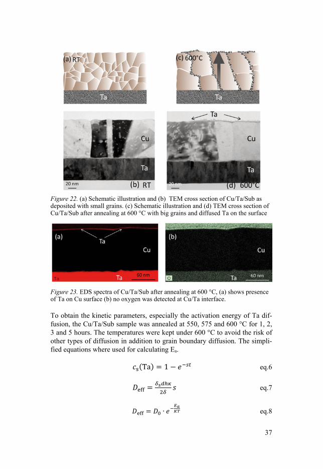
Un-capped Cu samples are extensively discussed in Paper III and IV. Metal stacks as it shown in detail in Table 6, were cleaved and annealed up to 800°C. Up to 500°C, all samples showed lower sheet resistance than as-deposited one due to grain growth of Cu, very similar to the Ag samples, see Figure 21. The Cu/Ta/Sub is behaving differently from Cu/TaN/Sub at tem-peratures over 500°C. RBS spectra for Cu/Ta/Sub show a Ta peak at higher energies which is belong to Ta on the surface. The SEM inspection of these samples shows that Ta reaches the Cu surface though grain boundaries of Cu and spreads out on the surface, see Figure 22. The EDS analysis of Cu/Ta/Sub confirms the presence of Ta on the surface and no oxygen at the interface which is shown in Figure 23. The Ta diffusion is increased by in-creasing the temperature up to 650°C. Above 700°C, RBS spectra shows a tail at the Ta surface peak which might be the onset of another mechanism of diffusion, for example bulk diffusion or protrusions of Ta into Cu. The dif-fused Ta spreads out on the surface and reacts with oxygen residue from the furnace and changes to TaxOy.
Figure 21. (a) SEM top view and (b) TEM cross section of Cu/Ta/Sub as deposited and c) SEM top view and d) TEM cross section of Cu/Ta/Sub after annealing at 600 °C
37
Figure 22. (a) Schematic illustration and (b) TEM cross section of Cu/Ta/Sub as deposited with small grains. (c) Schematic illustration and (d) TEM cross section of Cu/Ta/Sub after annealing at 600 °C with big grains and diffused Ta on the surface
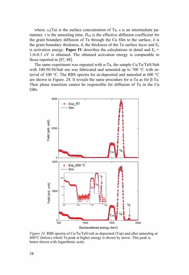
Figure 23. EDS spectra of Cu/Ta/Sub after annealing at 600 °C, (a) shows presence of Ta on Cu surface (b) no oxygen was detected at Cu/Ta interface.
To obtain the kinetic parameters, especially the activation energy of Ta dif-fusion, the Cu/Ta/Sub sample was annealed at 550, 575 and 600 °C for 1, 2, 3 and 5 hours. The temperatures were kept under 600 °C to avoid the risk of other types of diffusion in addition to grain boundary diffusion. The simpli-fied equations where used for calculating Ea.
Ta 1 eq.6
eq.7
∙ eq.8
38
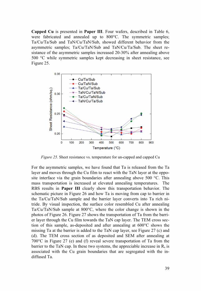
where, cs(Ta) is the surface concentration of Ta, s is an intermediate pa-rameter, t is the annealing time, Deff is the effective diffusion coefficient for the grain boundary diffusion of Ta through the Cu film to the surface, δ is the grain boundary thickness, δs the thickness of the Ta surface layer and Ea is activation energy. Paper IV describes the calculations in detail and Ea = 1.0±0.3 eV is obtained. The obtained activation energy is comparable to those reported in [87, 88].
The same experiment was repeated with α-Ta, the sample Cu/Ta/TaN/Sub with 100/50/30/Sub nm was fabricated and annealed up to 700 °C with in-terval of 100 °C. The RBS spectra for as-deposited and annealed at 600 °C are shown in Figure. 24. It reveals the same procedure for α-Ta as for β-Ta. Then phase transition cannot be responsible for diffusion of Ta in the Cu GBs.
Figure 24. RBS spectra of Cu/Ta/TaN/sub as deposited (Top) and after annealing at 600°C (below) which Ta peak at higher energy is shown by arrow. This peak is better shown with logarithmic scale.
39
Capped Cu is presented in Paper III. Four wafers, described in Table 6, were fabricated and annealed up to 800°C. The symmetric samples; Ta/Cu/Ta/Sub and TaN/Cu/TaN/Sub, showed different behavior from the asymmetric samples; Ta/Cu/TaN/Sub and TaN/Cu/Ta/Sub. The sheet re-sistance of the asymmetric samples increased 20-30% after annealing above 500 °C while symmetric samples kept decreasing in sheet resistance, see Figure 25.
Figure 25. Sheet resistance vs. temperature for un-capped and capped Cu
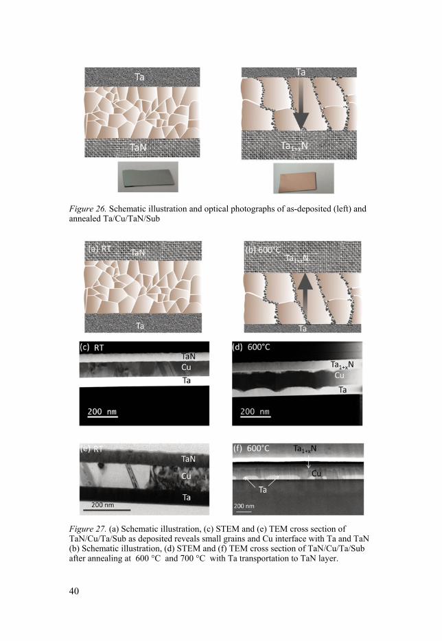
For the asymmetric samples, we have found that Ta is released from the Ta layer and moves through the Cu film to react with the TaN layer at the oppo-site interface via the grain boundaries after annealing above 500 °C. This mass transportation is increased at elevated annealing temperatures. The RBS results in Paper III clearly show this transportation behavior. The schematic picture in Figure 26 and how Ta is moving from cap to barrier in the Ta/Cu/TaN/Sub sample and the barrier layer converts into Ta rich ni-tride. By visual inspection, the surface color resembled Cu after annealing Ta/Cu/TaN/Sub sample at 800°C, where the color change is shown in the photos of Figure 26. Figure 27 shows the transportation of Ta from the barri-er layer through the Cu film towards the TaN cap layer. The TEM cross sec-tion of this sample, as-deposited and after annealing at 600°C shows the missing Ta at the barrier is added to the TaN cap layer, see Figure 27 (c) and (d). The TEM cross section of as deposited and SEM after annealing at 700°C in Figure 27 (e) and (f) reveal severe transportation of Ta from the barrier to the TaN cap. In these two systems, the appreciable increase in Rs is associated with the Cu grain boundaries that are segregated with the in-diffused Ta.
40
Figure 26. Schematic illustration and optical photographs of as-deposited (left) and annealed Ta/Cu/TaN/Sub
Figure 27. (a) Schematic illustration, (c) STEM and (e) TEM cross section of TaN/Cu/Ta/Sub as deposited reveals small grains and Cu interface with Ta and TaN (b) Schematic illustration, (d) STEM and (f) TEM cross section of TaN/Cu/Ta/Sub after annealing at 600 °C and 700 °C with Ta transportation to TaN layer.
41
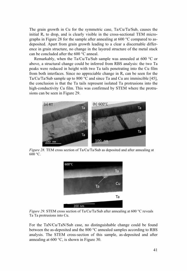
The grain growth in Cu for the symmetric case, Ta/Cu/Ta/Sub, causes the initial Rs to drop, and is clearly visible in the cross-sectional TEM micro-graphs in Figure 28 for the sample after annealing at 600 °C compared to as-deposited. Apart from grain growth leading to a clear a discernable differ-ence in grain structure, no change in the layered structure of the metal stack can be concluded after the 600 °C anneal.
Remarkably, when the Ta/Cu/Ta/Sub sample was annealed at 600 °C or above, a structural change could be inferred from RBS analysis: the two Ta peaks were reduced in height with two Ta tails penetrating into the Cu film from both interfaces. Since no appreciable change in Rs can be seen for the Ta/Cu/Ta/Sub sample up to 800 °C and since Ta and Cu are immiscible [45], the conclusion is that the Ta tails represent isolated Ta protrusions into the high-conductivity Cu film. This was confirmed by STEM where the protru-sions can be seen in Figure 29.
Figure 28. TEM cross section of Ta/Cu/Ta/Sub as deposited and after annealing at 600 °C.
Figure 29. STEM cross section of Ta/Cu/Ta/Sub after annealing at 600 °C reveals Ta Ta protrusions into Cu.
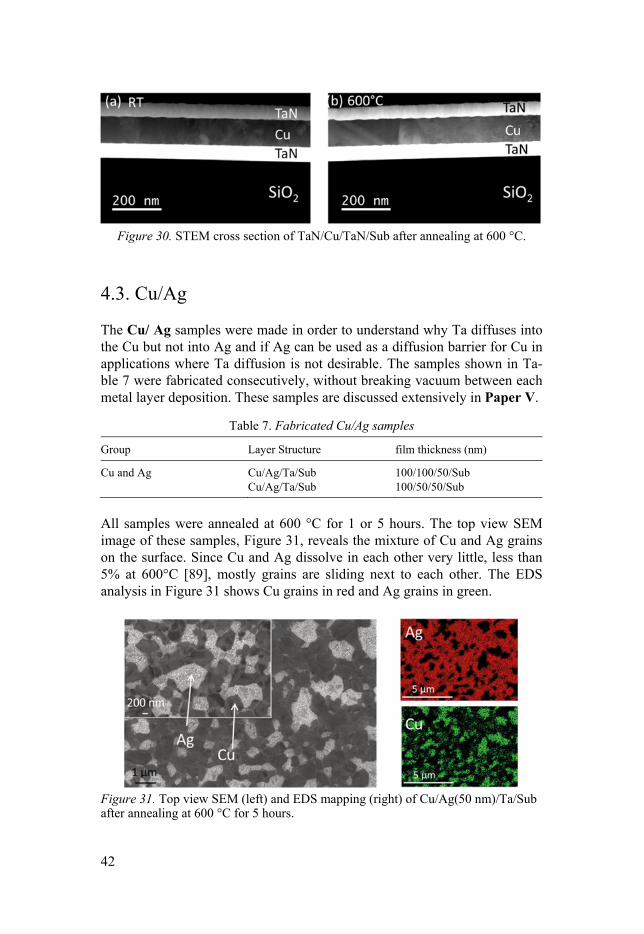
For the TaN/Cu/TaN/Sub case, no distinguishable change could be found between the as-deposited and the 800 °C annealed samples according to RBS analysis. The STEM cross-section of this sample, as-deposited and after annealing at 600 °C, is shown in Figure 30.
42
Figure 30. STEM cross section of TaN/Cu/TaN/Sub after annealing at 600 °C.
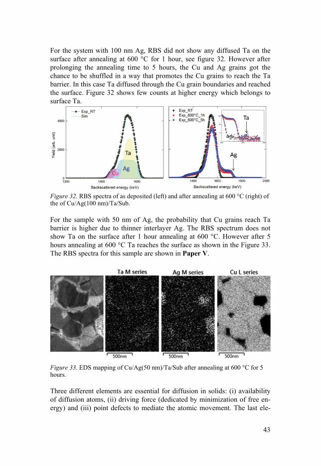
4.3. Cu/Ag
The Cu/ Ag samples were made in order to understand why Ta diffuses into the Cu but not into Ag and if Ag can be used as a diffusion barrier for Cu in applications where Ta diffusion is not desirable. The samples shown in Ta-ble 7 were fabricated consecutively, without breaking vacuum between each metal layer deposition. These samples are discussed extensively in Paper V.
Table 7. Fabricated Cu/Ag samples
Group Layer Structure film thickness (nm)
Cu and Ag Cu/Ag/Ta/Sub 100/100/50/Sub Cu/Ag/Ta/Sub 100/50/50/Sub
All samples were annealed at 600 °C for 1 or 5 hours. The top view SEM image of these samples, Figure 31, reveals the mixture of Cu and Ag grains on the surface. Since Cu and Ag dissolve in each other very little, less than 5% at 600°C [89], mostly grains are sliding next to each other. The EDS analysis in Figure 31 shows Cu grains in red and Ag grains in green.
Figure 31. Top view SEM (left) and EDS mapping (right) of Cu/Ag(50 nm)/Ta/Sub after annealing at 600 °C for 5 hours.
43
For the system with 100 nm Ag, RBS did not show any diffused Ta on the surface after annealing at 600 °C for 1 hour, see figure 32. However after prolonging the annealing time to 5 hours, the Cu and Ag grains got the chance to be shuffled in a way that promotes the Cu grains to reach the Ta barrier. In this case Ta diffused through the Cu grain boundaries and reached the surface. Figure 32 shows few counts at higher energy which belongs to surface Ta.
Figure 32. RBS spectra of as deposited (left) and after annealing at 600 °C (right) of the of Cu/Ag(100 nm)/Ta/Sub.
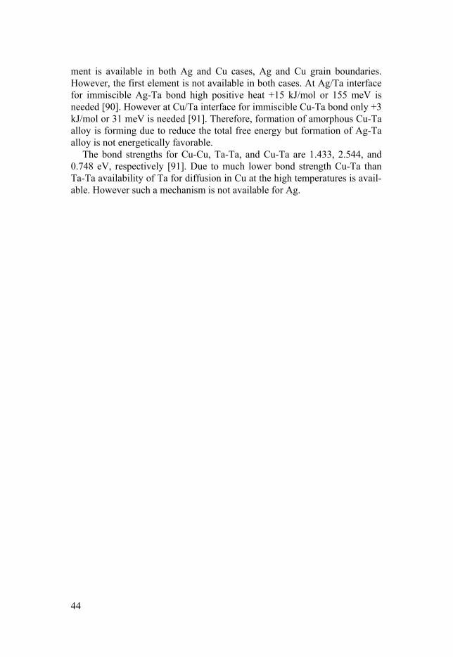
For the sample with 50 nm of Ag, the probability that Cu grains reach Ta barrier is higher due to thinner interlayer Ag. The RBS spectrum does not show Ta on the surface after 1 hour annealing at 600 °C. However after 5 hours annealing at 600 °C Ta reaches the surface as shown in the Figure 33. The RBS spectra for this sample are shown in Paper V.
Figure 33. EDS mapping of Cu/Ag(50 nm)/Ta/Sub after annealing at 600 °C for 5 hours.
Three different elements are essential for diffusion in solids: (i) availability of diffusion atoms, (ii) driving force (dedicated by minimization of free en-ergy) and (iii) point defects to mediate the atomic movement. The last ele-
44
ment is available in both Ag and Cu cases, Ag and Cu grain boundaries. However, the first element is not available in both cases. At Ag/Ta interface for immiscible Ag-Ta bond high positive heat +15 kJ/mol or 155 meV is needed [90]. However at Cu/Ta interface for immiscible Cu-Ta bond only +3 kJ/mol or 31 meV is needed [91]. Therefore, formation of amorphous Cu-Ta alloy is forming due to reduce the total free energy but formation of Ag-Ta alloy is not energetically favorable.
The bond strengths for Cu-Cu, Ta-Ta, and Cu-Ta are 1.433, 2.544, and 0.748 eV, respectively [91]. Due to much lower bond strength Cu-Ta than Ta-Ta availability of Ta for diffusion in Cu at the high temperatures is avail-able. However such a mechanism is not available for Ag.
45
5. Electromigration study
After an extensive investigation of different metal stacks at high tempera-tures, electromigration properties of these films were investigated. The re-sults on electromigataion are limited to Cu films. From the material study results and due to limitations in fabrication methods, it was decided to fabri-cate and characterize the samples defined in Table 8. The Cu thickness in this section is chosen to 300 nm to be closer to the real metallization goals.
Table 8. Fabricated metal stacks for patterning
Layer Structure Film thickness (nm) Anneal tempreture
TaN/Cu/TaN/Sub 50/300/50 No intentional annealing TaN/Cu/TaN/Sub 50/300/50 600°C after patterning TaN/Cu/Ta/Sub 50/300/50 No intentional annealing TaN/Cu/Ta/Sub 50/300/50 600°C after patterning
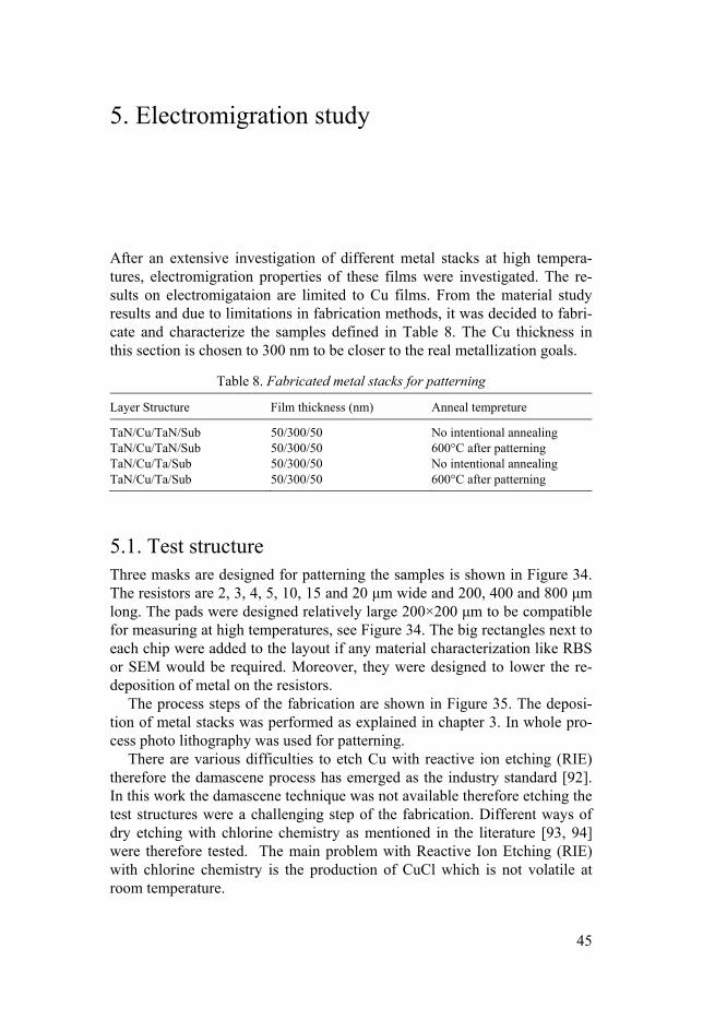
5.1. Test structure Three masks are designed for patterning the samples is shown in Figure 34. The resistors are 2, 3, 4, 5, 10, 15 and 20 μm wide and 200, 400 and 800 μm long. The pads were designed relatively large 200×200 μm to be compatible for measuring at high temperatures, see Figure 34. The big rectangles next to each chip were added to the layout if any material characterization like RBS or SEM would be required. Moreover, they were designed to lower the re-deposition of metal on the resistors.
The process steps of the fabrication are shown in Figure 35. The deposi-tion of metal stacks was performed as explained in chapter 3. In whole pro-cess photo lithography was used for patterning.
There are various difficulties to etch Cu with reactive ion etching (RIE) therefore the damascene process has emerged as the industry standard [92]. In this work the damascene technique was not available therefore etching the test structures were a challenging step of the fabrication. Different ways of dry etching with chlorine chemistry as mentioned in the literature [93, 94] were therefore tested. The main problem with Reactive Ion Etching (RIE) with chlorine chemistry is the production of CuCl which is not volatile at room temperature.
46
Figure 34. The mask layout for fabrication of EM resistors.
CuCl is quite corrosive and if it is not removed and completely passivat-ed, it will gradually damage the whole structure. It is suggested by Markert et el. [94] to increase the chuck temperature up to 200 °C to make CuCl vol-atile, however this was not possible in our PLASMA-THERM SLR tool. Sangheon Lee [93] proposed to remove CuCl in diluted HCl-6%, but this was not successful for our structures. Since after the wet removal and pas-sivation by CF4, still some CuCl was remaining which corroded the resistors.
The best solution showed to be etching the metallic layers physically. An ion beam etching system, CAIBE Oxford, was used with a beam current of 100mA, a beam voltage of 500 V, an accelerator voltage of 300 V, a wafer tilt of 0° and an etch time of 16-23 minutes. Due to having a uniform etch each wafer was rotated with 3 revolutions per minute (rpm). The mask was designed to limit the amount of material needed to be removed around the resistors and decrease the re-deposition during etching. After etching, the photoresist (PR) was stripped by 2 minutes of plasma stripper followed by wet removing in mr-Rem 400 PR-stripper with ultrasound. Next, two wafers were annealed in the Lesker sputter magnetron with a pressure below 1.3×10⁻⁵ Pa. In the next step, all samples were passivated with a 200 nm thick SiNx layer prepared by an Oxford plasma-enhanced chemical vapor deposition (PECVD) system at 300 °C. This passivation is essential since it protects the metals against oxidation during the measurements at elevated temperatures. The passivation layer on the pads was opened with RIE with power of 200 W and the PR was removed by plasma stripper for 10 min at 1000 W. A 0.5 μm Pd was deposited in a Lesker PVD system with an e-
47
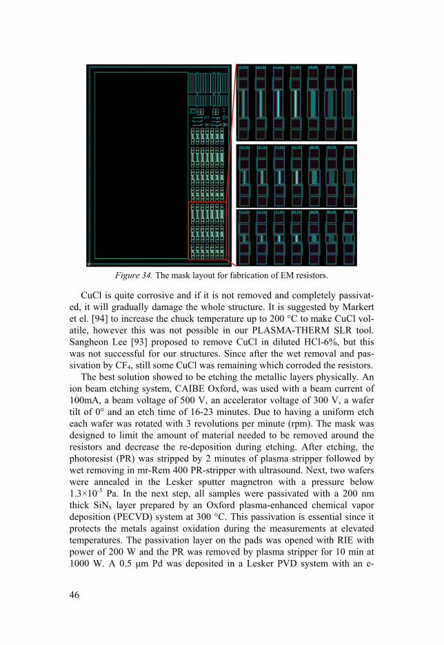
beam as a contact metal. A lift-off process was used for patterning the con-tact metal. Figure 36 shows various fabricated structures with different width.
Figure 35. The process flow for the preparation of EM resistors.
48
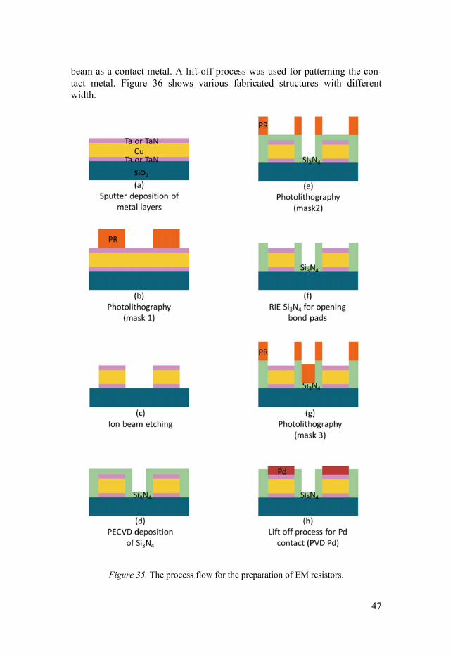
Figure 36. Optical micrograph of prepared EM resistors with 10 μm width and 200, 400 and 800 μm length.
5.2. Electrical characterization In Paper VI, electrical characterization in terms of electromigration robust-ness of barrier/Cu/Cap, as it is shown in Table 8, is presented. Resistance variation of the lines (resistors) was measured under thermal and electrical stress to accelerate life time of the test [95]. A probe-station (Karl Süss PM8) equipped with a hot chuck (Temptronic TP0315) was used. The meas-urements were performed using an HP 4142B parameter analyzer equipped with a high power (current-voltage) module 41420A. The measurement set-up was controlled by a PC using Metrics ICS software.
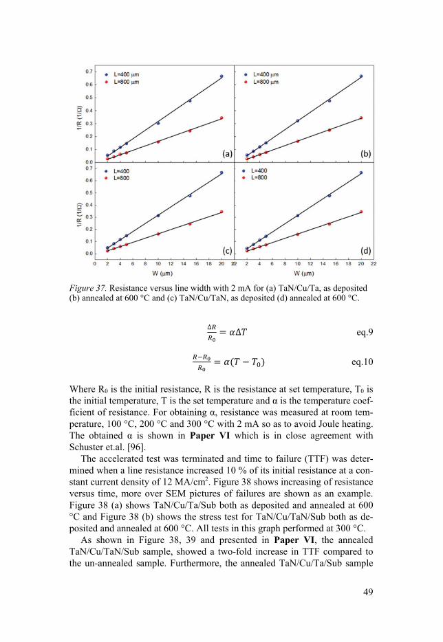
Initially, all wafers and chips were inspected with optical microscope for reasonable uniformity. The resistance of the lines for each wafer was meas-ured at low current (2 mA) to avoid stressing the resistor. Moreover, the width deviation, ΔW, was extrapolated from the intercept of each fitted line on the horizontal axis, see Figure 37. Width deviation calibration is essential in order to perform the accelerated test with consistent current density in all the wafers.
For measurements at elevated temperatures, the temperature was meas-ured by an external thermometer on the wafer in order to have a more accu-rate value. The electromigration measurements were executed with a current density of 12 MA/cm2. Such high current density adds an excessive Joule heating to the resistor which increases the temperature of the resistor. The real temperature of the resistor is needed in Black’s equation in order to cal-culate the activation energy. Different attempts for correcting the tempera-ture in order to have accurate resistor temperature are made in literatures [69, 96]. Equation 9 and 10 show relation between resistance and temperature.
49
Figure 37. Resistance versus line width with 2 mA for (a) TaN/Cu/Ta, as deposited (b) annealed at 600 °C and (c) TaN/Cu/TaN, as deposited (d) annealed at 600 °C.
∆ ∆ eq.9
eq.10
Where R0 is the initial resistance, R is the resistance at set temperature, T0 is the initial temperature, T is the set temperature and α is the temperature coef-ficient of resistance. For obtaining α, resistance was measured at room tem-perature, 100 °C, 200 °C and 300 °C with 2 mA so as to avoid Joule heating. The obtained α is shown in Paper VI which is in close agreement with Schuster et.al. [96].
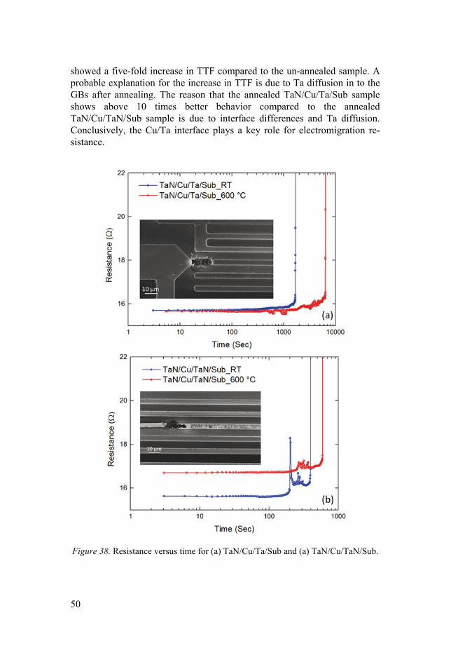
The accelerated test was terminated and time to failure (TTF) was deter-mined when a line resistance increased 10 % of its initial resistance at a con-stant current density of 12 MA/cm2. Figure 38 shows increasing of resistance versus time, more over SEM pictures of failures are shown as an example. Figure 38 (a) shows TaN/Cu/Ta/Sub both as deposited and annealed at 600 °C and Figure 38 (b) shows the stress test for TaN/Cu/TaN/Sub both as de-posited and annealed at 600 °C. All tests in this graph performed at 300 °C.
As shown in Figure 38, 39 and presented in Paper VI, the annealed TaN/Cu/TaN/Sub sample, showed a two-fold increase in TTF compared to the un-annealed sample. Furthermore, the annealed TaN/Cu/Ta/Sub sample
50
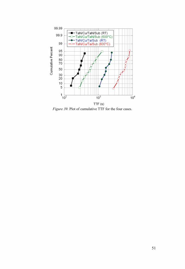
showed a five-fold increase in TTF compared to the un-annealed sample. A probable explanation for the increase in TTF is due to Ta diffusion in to the GBs after annealing. The reason that the annealed TaN/Cu/Ta/Sub sample shows above 10 times better behavior compared to the annealed TaN/Cu/TaN/Sub sample is due to interface differences and Ta diffusion. Conclusively, the Cu/Ta interface plays a key role for electromigration re-sistance.
Figure 38. Resistance versus time for (a) TaN/Cu/Ta/Sub and (a) TaN/Cu/TaN/Sub.
51
Figure 39. Plot of cumulative TTF for the four cases.

52
53
6. Summary
The aim of this thesis is to develop stable metallization for WBG devices especially SiC which can operate up to 500 °C. To achieve reliable metalli-zation, Ag and Cu as a main interconnect with Ta and/or TaN as a barrier and/or cap are selected. In this context, material properties and stability of these different metal stacks as well as the electromigration properties of Cu interconnects are explored. This thesis is divided into two major sections:
1. Material studies Various combinations of metal stacks are explored up to 800 °C. Un-capped Ag, Ag/Ta/Sub and Ag/TaN/sub is electrically and morphological stable up to 750 °C and 700 °C, respectively. The degradation of these stacks is major-ly due to agglomeration and void formation which explained in Paper I. By capping Ag the movement of Ag atoms along the surface is restricted and capping efficiently restrains agglomeration up to 800 °C. The nature of bar-rier metal is important for using Ag above 500 °C. Since β-Ta is metastable and transformation of β-Ta to stable α-Ta occurs between 600- 800 °C, this phase transformation can cause sever non uniformity on Ag film. Thus it is essential to deposit α-Ta from the beginning. Not only α-Ta is a stable phase but also it has lower resistivity and can be formed by depositing Ta on TaN. Paper II elaborates on capped Ag extensively.
Un-capped, Cu/Ta/Sub and Cu/TaN/sub is stable up to 800 °C which is the onset of agglomeration for later metal stack. Cu/Ta/Sub shows totally different behavior above 500 °C. Ta starts diffusing in to the Cu film through the Cu grain boundaries and spread on the surface of Cu. By increasing the annealing temperature, the amount of diffused Ta increases on the surface. The activation energy for grain boundary diffusion in Paper IV is evaluated Ea=1± 0.3 eV.
Symmetric capped Cu combination, TaN/Cu/TaN/sub and Ta/Cu/Ta/sub, show stable behaviour in terms of sheet resistance up to 800 °C. The former combination shows isolated Ta protrusions into the Cu film above 700 °C. Asymmetric capped Cu combination, Ta/Cu/TaN/sub and TaN/Cu/Ta/sub, shows slightly increase in sheet resistance above 500 °C however sheet re-sistance stays below as-deposited value even after annealing at 800 °C. Both combinations show diffusion from Ta layer to TaN layer trough grain
54
boundaries of Cu and forming Ta1+x N on the other side. Paper III elaborates on un-capped and capped Cu.
The combination of Cu/Ag/Ta/sub in Paper V confirms the need of liber-ate Ta atoms as one of the requirements in Ta diffusion. Since the formation of Ag-Ta bond is less energetically favorable due to large positive heat for-mation compared to Cu-Ta bond, Ta diffusion does not happen in Ag. In this metal stack configuration, Ta can diffuse to surface only if Cu grains move in a way that Cu and Ta bond and make Ta available for diffusion.
2. Electromigration studies Two different metal stacks TaN/Cu/TaN/sub and TaN/Cu/Ta/sub, were in-vestigated in order to explore electromigration properties of Cu with differ-ent Ta and TaN interfaces as well as the impact of Ta diffusion in to Cu. The TaN/Cu/Ta/Sub as-deposited and annealed at 600 °C have TTF activation energy, Ea, of 1 eV and TaN/Cu/TaN/Sub structures as-deposited and an-nealed at 600 °C have TTF activation energy, Ea, of 0.47 eV. The TaN/Cu/Ta/Sub shows 2-fold higher activation energy and a 10-fold longer lifetime for TaN/Cu/TaN/Sub structures. The electromigration results are shown in Paper VI.
The knowledge gained from our extensive study of the high-temperature materials behaviors of the interconnect schemes based on Cu and Ag will be indispensable for exploring their electromigration properties. With the lim-ited resources, we have made an initial attempt with Cu interconnect and obtained useful indications regarding the influence of Ta diffusion and de-tailed Cu interfaces. A more systematic investigation is clearly required con-cerning, e.g., more practical adhesion and capping solutions than used so far for Cu interconnect. Moreover, a comparison between electroplated Cu (the industry-dominant approach) and sputter-deposited Cu, with different Ta and/or TaN interfaces, can be of importance. Also of great interest is the electromigration behaviour of the Ag-based interconnect. Different adhesion and capping solutions are again anticipated to be critical although Ta diffu-sion does not seem to take place in Ag.
55
7. Svensk sammanfattning
Komponenter gjorda i halvledarmaterial med stort bandgap (WBG), i syn-nerhet kiselkarbid (SiC) och galliumnitrid (GaN), har under senare tid ut-vecklats och optimerats för att kunna fungera vid mycket höga temperaturer och under svåra förhållanden. Drivet av de ständigt ökande kraven på höga temperaturer för elektronik i områden såsom energiproduktion, flygteknik och inom flygindustrin, har WBG-komponenter stadigt blivit mer värme-toleranta. Emellertid begränsas nuvarande WBG-komponenter av den metal-lurgiska stabiliteten av de ledningar som finns på chipet. Hållbarheten och tillförlitligheten hos t ex metall-halvledarkontakter och ledningar är faktorer som för närvarande begränsar användningen vid hög temperatur för dessa komponenter.
I denna doktorsavhandling har olika experimentella forskningsstudier ut-förts för att undersöka möjliga lösningar för att övervinna ovan nämna be-gränsningar i metalliseringssystemen så att WBG-komponenter ska kunna arbeta vid mycket höga temperaturer, dvs åtminstone upp till 500 °C. För att uppnå tillförlitlighet så har i huvudsak silver (Ag) and koppar (Cu) studerats med både Ta och/eller TaN som skyddsbarriär och skyddslager. I detta sammanhang har materialegenskaper och stabiliteten för dessa olika metall-kombinationer undersökts. Även elektromigration (dvs förmågan att leda stora strömmar utan att förstöras) har undersökts för de kopparbaserade me-tallkombinationerna.
Denna avhandling är uppdelad i två huvuddelar. I första delen om materi-alstudier är olika kombinationer av metallerna utforskade upp till 800 °C. Resultaten visar att Ag utan passiveringsmetall på toppen, dvs i kombinat-ionerna Ag/Ta/Sub och Ag/TaN/Sub är helt elektriskt och morfologiskt sta-bila upp till åtminstone 600 °C. Men degradering av Ag/Ta/Sub och Ag/TaN/Sub filmer sker vid 750 °C respektive 700 °C, främst till följd av att tomrum bildas i filmen och att Ag-filmen agglomererar. Papper I i avhand-lingen beskriver i detalj studien av Ag utan skyddsmetall på toppen.
Det visar sig dock att en tunn skyddsmetall på toppen av silvret (som ett lock), effektivt begränsar masstransport längs Ag-ytan och även effektivt förhindrar Ag att förångas vid höga temperaturer, som upp till 800 °C. Att skydda ytan är avgörande för att stabilisera Ag-filmerna elektriskt och mor-fologiskt. Skillnaden mellan Ta och TaN som toppskikt visade sig vara för-sumbar. Emellertid spelar egenskaperna hos skyddsbarriären (den tunna metallfilmen under silvret som ska förhindra diffusion till det underliggande-
56
substratet) under Ag-filmen en betydande roll. Möjligheten till en β-till-α fasövergång i en Ta-barriär visas ha katastrofala följder för Ag-filmen och topplagrets morfologi. I applikationer där stabiliteten vid hög temperatur är av betydelse och där Ta-barriär är att föredra är det därför viktigt att se till att den initialt deponerade Ta-barriären har α-fasstruktur. Papper II presenterar en utförlig studie om Ag med skyddsbarriär.
Vad gäller kopparmetallisering visar det sig att Cu/Ta/Sub och Cu/TaN/Sub är stabila upp till 800 °C, vilket är då agglomerering börjar för den senare metallkombinationen. Cu/Ta/Sub har däremot ett helt annat bete-ende över 500 °C. Ta lämnar Ta-skiktet och rör sig genom Cu-filmen till det motsatta gränssnittet via korngränserna. Ta diffunderar via korngränserna genom Cu-filmen och sprider ut sig på ytan av Cu-kornen, för att vid 650 °C helt täcka ytan. Aktiveringsenergin för korngränsdiffusionen beräknas i Papper IV till 1.0±0.3 eV. Ta diffusion i korngränserna leder till stabilise-ring av Cu-kornstorlek på 360 nm och en ökning i ytresistansen hos metall-kombinationen.
Symmetriska metallkombinationer med TaN/Cu/TaN/Sub och Ta/Cu/Ta/Sub, uppvisar ett stabilt beteende när det gäller ytresistans upp till 800 °C. Den tidigare kombinationen visar isolerade områden med utträng-ning av Ta i Cu-filmen över 700 °C. Asymmetriska kombinationer, som Ta/Cu/TaN/Sub och TaN/Cu/Ta/Sub, uppvisar något ökad ytresistans över 500 °C men ytresistansen håller sig under värdet för filmer som inte är vär-mebehandlade, även efter behandling vid 800 °C. I båda kombinationerna sker diffusion från Ta-skikt till TaN-skikt via diffusion i korngränserna och Ta bildar Ta1+x N på den andra sidan. Papper III studera Cu både med och utan skyddande topplager.
Alla metallkombinationer med Cu i kontakt med Ta på endera sidan och TaN eller ingenting alls på den andra uppvisar detta diffusionsbeteende. Därför måste metallstacken stabiliseras med en värmebehandling vid eller över den högsta förväntade temperaturen för komponenten.
Skillnaden i beteende gällande Ta-diffusion för Cu- och Ag-filmer under-söktes i Papper V. Medan Ta diffusion i Cu filmer följer den vanliga mek-anismen under påverkan av en drivkraft via de givna kinetiska diffusionsvä-garna längs korngränserna, så tillskrivs frånvaron av Ta diffusion i Ag-filmer bristen på tillgängliga Ta-atomer vid Ag/Ta gränssnittet även om de två materialen är i intim kontakt. Ta-Ta bindningen är så stark att det skulle kräva temperaturer mycket högre än smältpunkten för Ag (962 °C) för att frigöra Ta atomer från det extremt hårt bundna Ta (av andra Ta-atomer).
Vid Cu/Ta-gränssnittet emellertid, har den energetiskt fördelaktiga bild-ningen av Cu-Ta bindning en mycket lägre bindningsstyrka (omkring en tredjedel av Ta-Ta bindningsstyrka). Det blir då ett effektivt mellansteg för att lösa ut Ta-atomer för diffusion. Denna skillnad i Ta-diffusion skulle kunna utnyttjas i tillämpningar om man använder Ag som en diffusionsbar-riär för att förhindra Ta från att diffundera in i Cu.
57
Andra delen i avhandlingen handlar om elektromigration. I dessa studier har två distinkta Cu-system studerats: asymmetrisk med Ta på ena sidan och TaN på den andra och symmetriska med antingen Ta eller TaN på båda si-dor, detta för att undersöka påverkan av de olika gränsytorna samt eventuell Ta-diffusion genom Cu-filmerna.
TaN/Cu/Ta/Sub, med eller utan värmebehandling vid 600 °C har en TTF (time-to-failure) aktiveringsenergi, Ea, på 1 eV, medans TaN/Cu/TaN/Sub strukturer, med eller utan värmebehandling vid 600 °C, har en TTF aktive-ringsenergi, Ea, på 0.47 eV. TaN/Cu/Ta/Sub uppvisar dubbelt så hög aktive-ringsenergi och 10 gånger längre livslängd än TaN/Cu/TaN/Sub strukturena. Studien om elektromigration redovisas i Papper VI.
Sammanfattningsvis, genom att belägga eller omsluta Ag- eller Cu-filmerna med skyddande lager av Ta eller TaN förbättras både de elektriska egenskaperna och den morfologiska stabilitetet avsevärt vid höga temperatu-rer. Dessutom har det visats i denna avhandling att Cu med åtminstone ett Ta/Cu gränssnitt kan ha 10-faldigt längre elektrisk livslängd jämfört med Cu med ett Cu/TaN gränssnitt.

58
59
Acknowledgments
This thesis is a summary of my research work during the past few years as a Ph.D student at Uppsala University. During these years I have received countless help and support from many wonderful people. The financial sup-port of Swedish Foundation for Strategic Research (SSF) and the Swedish Research Council (VR) is also acknowledged.
First of all, I am most grateful to my excellent supervisors: Shi-Li Zhang for his constant support, encouragement and excellent guidance throughout the project; Hans Norström for his wisdom, amazing attitude and managing approach in scientific research; Jörgen Olsson for his patience and support throughout the project; Ulf Smith for his knowledge, continues encourage-ment and motivation; Örjan Vallin for his valuable support and guidance in experiments.
I would like to express my appreciation to: Mats Hagberg, John Halonen, and Niclas Lindvall at Chalmers; Dominique Mangelinck and Marion Des-coins at METSA; Reza Nikpars at KTH; Tomas Nyberg, Fredrik Gus-tavsson, Anders Hallén, Daniel Primetzhofer, Tomas Kubart, Zhen Zhang, Uwe Zimmermann and Marianne Asplund for their professional help and support; whole MSL team for their great technical help and support in the clean room.
I would like to thank Sara, Milena, Erik, Li, Toppie, JJ and Bagge for the fun lunches, after-works, talks and laughs. I would like to thank my wonder-ful colleagues and friends at KTH: Shabnam, Pooria, Nikki, Arash, Sam, Kostas, Hossein, Roody, Marjan, Ahmad, Mohsen and Milad for hilarious talks and laughs. I would also like to thank Malkolm, Mandy, Darcy, Piotr, Jessica, Valeria, Saman, Andrej and other colleagues and friends for mind refreshing and fun talks. I would also like to thank all my colleagues at FTE.
Finally, I would like to express my sincere gratitude to my lovely parents, Shima and Mehdi for their endless love and support.
Shabnam Mardani Uppsala, September 2016

60
61
References
1. Shenai, K., M. Dudley, and R.F. Davis, Current Status and Emerging Trends in Wide Bandgap (WBG) Semiconductor Power Switching Devices. Ecs Journal of Solid State Science and Technology, 2013. 2(8): p. N3055-N3063.
2. Neudeck, Silicon Carbide thecnology. 2006. 3. Neudeck, P.G., et al., Extreme temperature 6H-SiC JFET integrated
circuit technology. Physica Status Solidi a-Applications and Materials Science, 2009. 206(10): p. 2329-2345.
4. Carl W Chang, P.G.N., Glenn M Beheim, David Spry, Current-Voltage Testing of Candidate Dielectric Materials for 500 °C SiC. Integrated Circuits. 2008.
5. F.P McCluskey, R.G., and T. Podlesak,, High Temperature Electronics. 1997, New York: CRC Press.
6. Mark, C., Clear road ahead? Power Engineer, 2004. 18(4): p. 34-38. 7. Johnson, R.W., et al., The changing automotive environment: High-
temperature electronics. Ieee Transactions on Electronics Packaging Manufacturing, 2004. 27(3): p. 164-176.
8. Buttay, C., et al., State of the art of high temperature power electronics. Materials Science and Engineering B-Advanced Functional Solid-State Materials, 2011. 176(4): p. 283-288.
9. Neudeck, P.G., R.S. Okojie, and L.Y. Chen, High-temperature electronics - A role for wide bandgap semiconductors? Proceedings of the Ieee, 2002. 90(6): p. 1065-1076.
10. Eden, R., The World Market for Silicon Carbide & Gallium Nitride Power Semiconductors, in IHS. 2013: Wellingborough.
11. Trew, R.J., SiC and GaN transistors - Is there one winner for microwave power applications? Proceedings of the Ieee, 2002. 90(6): p. 1032-1047.
12. Trew, R.J., J.B. Yan, and P.M. Mock, The Potential of Diamond and Sic Electronic Devices for Microwave and Millimeter-Wave Power Applications. Proceedings of the Ieee, 1991. 79(5): p. 598-620.
13. Elasser, A. and T.P. Chow, Silicon carbide benefits and advantages for power electronics circuits and systems. Proceedings of the Ieee, 2002. 90(6): p. 969-986.
14. Baliga, B.J., Trends in power semiconductor devices. Ieee Transactions on Electron Devices, 1996. 43(10): p. 1717-1731.
15. E.H. Amalu, N.N.E.a.R.S.B., High temperature electronics R&D challenges and trends in materials, packaging and interconnection technology. 2009.
62
16. Castro, J.W.a.G., High Temperature Electronics pose Design and Reliability Challenges. 2012.
17. Werner, M.R. and W.R. Fahrner, Review on materials, microsensors, systems, and devices for high-temperature and harsh-environment applications. Ieee Transactions on Industrial Electronics, 2001. 48(2): p. 249-257.
18. Flandre, P.F.A.T.B.G.D., SOI technology for high-temperature applications. IEEE International Electron Devices, 1992: p. 353 - 356
19. Kappert, H., et al., High Temperature SOI CMOS Technology and Circuit Realization for Applications up to 300 degrees C. 2015 Ieee International Symposium on Circuits and Systems (Iscas), 2015: p. 1162-1165.
20. LANNI, L., Silicon Carbide Bipolar Integrated Circuits for High Temperature Applications. 2014.
21. Smedfors, K., Ohmic Contacts for High Temperature Integrated Circuits in Silicon Carbide. 2014.
22. Pensl, W.J.C.a.G., Physical Properties of SiC. 1997. 23. Zetterling, C.-M., process technology for silicon carbide devices.
2002. 24. Corinne, et al., High frequency simulation and characterization of
advanced Copper interconnects 25. Venkatesan, S., et al., A high performance 1.8V, 0.20 mu m CMOS
technology with copper metallization. International Electron Devices Meeting - 1997, Technical Digest, 1997: p. 769-772.
26. Lloyd, J.R. and J.J. Clement, Electromigration in Copper Conductors. Thin Solid Films, 1995. 262(1-2): p. 135-141.
27. Edelstein, D., et al., Full copper wiring in a sub-0.25 mu m CMOS ULSI technology. International Electron Devices Meeting - 1997, Technical Digest, 1997: p. 773-776.
28. Pai, P.L. and C.H. Ting, Selective Electroless Copper for Vlsi Interconnection. Ieee Electron Device Letters, 1989. 10(9): p. 423-425.
29. Small, M.B. and D.J. Pearson, On-Chip Wiring for Vlsi - Status and Directions. Ibm Journal of Research and Development, 1990. 34(6): p. 858-867.
30. Radzimski, Z.J., et al., Directional copper deposition using dc magnetron self-sputtering. Journal of Vacuum Science & Technology B, 1998. 16(3): p. 1102-1106.
31. Mikhail Baklanov , P.S.H., Ehrenfried Zschech, Advanced Interconnects for ULSI Technology.
32. Murarka, S.P. and S.W. Hymes, Copper Metallization for Ulsi and Beyond. Critical Reviews in Solid State and Materials Sciences, 1995. 20(2): p. 87-124.
33. Ryu, C., et al., Effect of texture on the electromigration of CVD copper. 1997 Ieee International Reliability Physics Symposium Proceedings - 35th Annual, 1997: p. 201-205.
63
34. Murarka, S.P., metallization theory and practice for vlsi and ulsi. 35. Istratov, A.A., et al., Intrinsic diffusion coefficient of interstitial
copper in silicon. Physical Review Letters, 1998. 81(6): p. 1243-1246.
36. Adams, D. and T.L. Alford, Encapsulated silver for integrated circuit metallization. Materials Science & Engineering R-Reports, 2003. 40(6): p. 207-250.
37. Daniel Adams, J.W.M., and Terry L. Alford, Silver Metallization: Stability and Reliability.
38. Nicolet, M.A., Diffusion Barriers in Thin-Films. Thin Solid Films, 1978. 52(3): p. 415-443.
39. Braud, F., et al., Ti-Diffusion Barrier in Cu-Based Metallization. Applied Surface Science, 1995. 91(1-4): p. 251-256.
40. Mercier, M., et al., Evaluation of sputtered tungsten as diffusion barrier materials for copper. Defect and Diffusion Forum, 1997. 143: p. 1285-1290.
41. Laurila, T., et al., Failure mechanism of Ta diffusion barrier between Cu and Si. Journal of Applied Physics, 2000. 88(6): p. 3377-3384.
42. Riedel, S., et al., Influence of different treatment techniques on the barrier properties of MOCVD TiN against copper diffusion. Microelectronic Engineering, 2001. 55(1-4): p. 213-218.
43. Hecker, M., et al., Influence of N content on microstructure and thermal stability of Ta-N thin films for Cu interconnection. Thin Solid Films, 2002. 414(2): p. 184-191.
44. Hecker, M., et al., Effect of annealing on the microstructure of ultrathin tungsten nitride diffusion barriers for copper metallization. Microelectronic Engineering, 2002. 64(1-4): p. 269-277.
45. Subramanian, P.R.a.L., D.E, The Cu-Ta (Copper-Tantalum) System. Bull. Alloy Phase Diagrams, 1989. 10: p. 652–655.
46. Kaufman, L., Coupled Thermochemical and Phase-Diagram Data for Tantalum Based Binary-Alloys. Calphad-Computer Coupling of Phase Diagrams and Thermochemistry, 1991. 15(3): p. 243-259.
47. Edelstein, D., et al., An optimal liner for copper damascene interconnects. Advanced Metallization Conference 2001 (Amc 2001), 2001: p. 541-547.
48. Holloway, K., et al., Tantalum as a Diffusion Barrier between Copper and Silicon - Failure Mechanism and Effect of Nitrogen Additions. Journal of Applied Physics, 1992. 71(11): p. 5433-5444.
49. Stavrev, M., et al., Behavior of thin Ta-based films in the Cu/barrier/Si system. Journal of Vacuum Science & Technology a-Vacuum Surfaces and Films, 1999. 17(3): p. 993-1001.
50. Lane, M., et al., Adhesion and reliability of copper interconnects with Ta and TaN barrier layers. Journal of Materials Research, 2000. 15(1): p. 203-211.
64
51. Liu, L., Y. Wang, and H. Gong, Annealing effects of tantalum films on Si and SiO2/Si substrates in various vacuums. Journal of Applied Physics, 2001. 90(1): p. 416-420.
52. Chen, L., B. Ekstrom, and J. Kelber, The effect of surface oxides on Cu/Ta interfacial interactions. Advanced Interconnects and Contacts, 1999. 564: p. 287-292.
53. Hubner, R., et al., Structure and thermal stability of graded Ta-TaN diffusion barriers between Cu and SiO2. Thin Solid Films, 2003. 437(1-2): p. 248-256.
54. Loh, S.W., et al., Study of copper diffusion into Ta and TaN barrier materials for MOS devices. Thin Solid Films, 2004. 462: p. 240-244.
55. Frety, N., et al., Copper diffusion into silicon substrates through TaN and Ta/TaN multilayer barriers. Journal of Phase Equilibria and Diffusion, 2006. 27(6): p. 590-597.
56. Smirnov, Y.M. and V.A. Finkel, Crystal Structure of Tantalum Niobium and Vanadium at 110--400 Degrees K. Soviet Physics Jetp-Ussr, 1966. 22(4): p. 750-&.
57. Baker, P.N., Preparation and Properties of Tantalum Thin-Films. Thin Solid Films, 1972. 14(1): p. 3-25.
58. Cheng, J.Y. and L.J. Chen, Growth-Kinetics of Amorphous Interlayers by Solid-State Diffusion in Ultrahigh-Vacuum Deposited Polycrystalline Nb and Ta Thin-Films on (111)Si. Journal of Applied Physics, 1991. 69(4): p. 2161-2168.
59. Fischer, D., et al., AFM characterization of Ta-based diffusion barriers for use in future semiconductor metallization. Surface and Interface Analysis, 1997. 25(7-8): p. 522-528.
60. Hubner, R., et al., Comparison of the annealing behavior of thin Ta films deposited onto Si and SiO2 substrates. Analytical and Bioanalytical Chemistry, 2004. 379(4): p. 568-575.
61. Mutscheller, A., et al., Effect of Deposition Conditions on Intrinsic Stress, Phase-Transformation and Stress-Relaxation in Tantalum Thin-Films. Thin Films : Stress and Mechanical Properties Iii, 1992. 239: p. 51-56.
62. Clevenger, L.A., et al., The Relationship between Deposition Conditions, the Beta to Alpha Phase-Transformation, and Stress-Relaxation in Tantalum Thin-Films. Journal of Applied Physics, 1992. 72(10): p. 4918-4924.
63. Hoogeveen, R., et al., Texture and phase transformation of sputter-deposited metastable Ta films and Ta/Cu multilayers. Thin Solid Films, 1996. 275(1-2): p. 203-206.
64. Feinstein, L.G. and R.D. Huttemann, Factors Controlling Structure of Sputtered Ta Films. Thin Solid Films, 1973. 16(2): p. 129-145.
65. Fryer, E.G.C.a.P.M. 1993: USA. 66. Fiks, V.B., On the Mechanism of the Mobility of Ions in Metals.
Soviet Physics-Solid State, 1959. 1(1): p. 14-28.
65
67. Scorzoni, A., et al., Electromigration in Thin-Film Interconnection Lines - Models, Methods and Results. Materials Science Reports, 1991. 7(4-5): p. 143-220.
68. Lienig, J. and G. Jerke, Embedded tutorial: Electromigration-aware physical design of integrated circuits. 18th International Conference on Vlsi Design, Proceedings, 2005: p. 77-82.
69. Frye, R., et al., Electromigration Measurements in Thin-Film IPD and eWLB Interconnections. 2012 Ieee 62nd Electronic Components and Technology Conference (Ectc), 2012: p. 1304-1311.
70. Young, D. and A. Christou, Failure-Mechanism Models for Electromigration. Ieee Transactions on Reliability, 1994. 43(2): p. 186-192.
71. Vairagar, A.V., S.G. Mhaisalkar, and A. Krishnamoorthy, Electromigration behavior of dual-damascene Cu interconnects-structure, width, and length dependences. Microelectronics Reliability, 2004. 44(5): p. 747-754.
72. Hayashi, M., S. Nakano, and T. Wada, Dependence of copper interconnect electromigration phenomenon on barrier metal materials. Microelectronics Reliability, 2003. 43(9-11): p. 1545-1550.
73. Li, B.Z., et al., Reliability challenges for copper interconnects. Microelectronics Reliability, 2004. 44(3): p. 365-380.
74. Black, J.R., Mass transport of aluminum by momentum exchange with conducting electrons. 2005 Ieee International Reliability Physics Symposium Proceedings - 43rd Annual, 1967: p. 1-6.
75. Black, J.R., Electromigration - a Brief Survey and Some Recent Results. Ieee Transactions on Electron Devices, 1969. Ed16(4): p. 338-&.
76. Wasa, K., M. Kitabatake, and H. Adachi, Thin Films Material Technology-Sputtering of Compound Materials. 2004: Springer-Verlag Berlin Heidelberg.
77. Ohring, M., Materials Science of Thin Films, in Materials Science of Thin Films 2002.
78. Arthur H Landrock, S.M.R., J. J. Cuomo, William Dickson Westwood, Handbook of Plasma Processing Technology: Fundamentals, Etching, Deposition, and Surface Interactions. 1990.
79. Behrisch, R., Sputtering by Particle Bombardment I. 1981. 80. Kern, W., Cleaning Solutions Based on Hydrogen-Peroxide for Use
in Silicon Semiconductor Technology. Current Contents/Engineering Technology & Applied Sciences, 1983(11): p. 18-18.
81. Mayer, M., Ion beam analysis of rough thin films. Nuclear Instruments & Methods in Physics Research Section B-Beam Interactions with Materials and Atoms, 2002. 194(2): p. 177-186.
82. Zhang, Y.W., et al., Detection efficiency of time-of-flight energy elastic recoil detection analysis systems. Nuclear Instruments & Methods in Physics Research Section B-Beam Interactions with Materials and Atoms, 1999. 149(4): p. 477-489.
66
83. Rosenstock, Z. and I. Riess, Preparation of oxide thin films by controlled diffusion of oxygen atoms. Solid State Ionics, 2000. 136: p. 921-926.
84. Rosenstock, Z., I. Feldman, and I. Riess, Solid state devices based on thin films of Cu2O show a new type of I-V relations. Solid State Ionics, 2004. 175(1-4): p. 375-378.
85. Murarka, S.P., et al., Advanced Multilayer Metallization Schemes with Copper as Interconnection Metal. Thin Solid Films, 1993. 236(1-2): p. 257-266.
86. Graedel, T.E., Corrosion Mechanisms for Silver Exposed to the Atmosphere. Journal of the Electrochemical Society, 1992. 139(7): p. 1963-1970.
87. Erdelyi, G., et al., Investigation of Ta grain boundary diffusion in copper by means of Auger electron spectroscopy. Thin Solid Films, 2004. 459(1-2): p. 303-307.
88. Lakatos, A., et al., Investigations of diffusion kinetics in Si/Ta/Cu/W and Si/Co/Ta systems by secondary neutral mass spectrometry. Vacuum, 2010. 84(7): p. 953-957.
89. Baker, T.B.M.J.L.M.L.H.B.H., Binary alloy phase diagrams. 1986, Metals Park, Ohio.
90. Shen, Y.X., et al., Structural stability and the correlation of lattice constant versus tantalum concentration of the Ag-based Fcc solid solutions studied by molecular dynamics simulation. Japanese Journal of Applied Physics Part 1-Regular Papers Short Notes & Review Papers, 2004. 43(5A): p. 2589-2593.
91. Gong, H.R. and B.X. Liu, Interface stability and solid-state amorphization in an immiscible Cu-Ta system. Applied Physics Letters, 2003. 83(22): p. 4515-4517.
92. Andricacos, P.C., et al., Damascene copper electroplating for chip interconnections. Ibm Journal of Research and Development, 1998. 42(5): p. 567-574.
93. Lee, S. and Y. Kuo, Chlorine plasma/copper reaction in a new copper dry etching process. Journal of the Electrochemical Society, 2001. 148(9): p. G524-G529.
94. Markert, M., et al., High throughput, high quality dry etching of copper/barrier film stacks. Microelectronic Engineering, 2000. 50(1-4): p. 417-423.
95. Aubel, O., W. Hasse, and M. Hommel, Highly accelerated electromigration lifetime test (HALT) of copper. Ieee Transactions on Device and Materials Reliability, 2003. 3(4): p. 213-217.
96. Schuster, C.E., M.G. Vangel, and H.A. Schafft, Improved estimation of the resistivity of pure copper and electrical determination of thin copper film dimensions. Microelectronics Reliability, 2001. 41(2): p. 239-252.

Acta Universitatis UpsaliensisDigital Comprehensive Summaries of Uppsala Dissertationsfrom the Faculty of Science and Technology 1406
Editor: The Dean of the Faculty of Science and Technology
A doctoral dissertation from the Faculty of Science andTechnology, Uppsala University, is usually a summary of anumber of papers. A few copies of the complete dissertationare kept at major Swedish research libraries, while thesummary alone is distributed internationally throughthe series Digital Comprehensive Summaries of UppsalaDissertations from the Faculty of Science and Technology.(Prior to January, 2005, the series was published under thetitle “Comprehensive Summaries of Uppsala Dissertationsfrom the Faculty of Science and Technology”.)
Distribution: publications.uu.seurn:nbn:se:uu:diva-300796
ACTAUNIVERSITATIS
UPSALIENSISUPPSALA
2016


![TANTALUM-BASED DIFFUSION BARRIERS FOR COPPER METALLIZATION · 2017-04-28 · many polymers used as dielectric layers [7,8]. Moreover, copper corrodes easily upon ... metallization](https://img.pdfslide.us/doc/110x75/5f73949b454c884fb754b005/tantalum-based-diffusion-barriers-for-copper-metallization-2017-04-28-many-polymers.jpg)