Embed Size (px)
Citation preview
University of Birmingham
Copper Metallization of Gold NanostructureActivated Polypyrrole by Electroless DepositionPandey, Richa; Jian, Nan; Inberg, Alexandra; Palmer, Richard; Shacham-Diamand, Yosi
DOI:10.1016/j.electacta.2017.06.157
License:Creative Commons: Attribution-NonCommercial-NoDerivs (CC BY-NC-ND)
Document VersionPeer reviewed version
Citation for published version (Harvard):Pandey, R, Jian, N, Inberg, A, Palmer, R & Shacham-Diamand, Y 2017, 'Copper Metallization of GoldNanostructure Activated Polypyrrole by Electroless Deposition', Electrochimica Acta, vol. 246, pp. 1210-1216.https://doi.org/10.1016/j.electacta.2017.06.157
Link to publication on Research at Birmingham portal
General rightsUnless a licence is specified above, all rights (including copyright and moral rights) in this document are retained by the authors and/or thecopyright holders. The express permission of the copyright holder must be obtained for any use of this material other than for purposespermitted by law.
•Users may freely distribute the URL that is used to identify this publication.•Users may download and/or print one copy of the publication from the University of Birmingham research portal for the purpose of privatestudy or non-commercial research.•User may use extracts from the document in line with the concept of ‘fair dealing’ under the Copyright, Designs and Patents Act 1988 (?)•Users may not further distribute the material nor use it for the purposes of commercial gain.
Where a licence is displayed above, please note the terms and conditions of the licence govern your use of this document.
When citing, please reference the published version.
Take down policyWhile the University of Birmingham exercises care and attention in making items available there are rare occasions when an item has beenuploaded in error or has been deemed to be commercially or otherwise sensitive.
If you believe that this is the case for this document, please contact [email protected] providing details and we will remove access tothe work immediately and investigate.
Download date: 30. May. 2020
Accepted Manuscript
Title: Copper Metallization of Gold Nanostructure ActivatedPolypyrrole by Electroless Deposition
Authors: Richa Pandey, Nan Jian, Alexandra Inberg, RichardE. Palmer, Yosi Shacham-Diamand
PII: S0013-4686(17)31395-6DOI: http://dx.doi.org/doi:10.1016/j.electacta.2017.06.157Reference: EA 29795
To appear in: Electrochimica Acta
Received date: 30-1-2017Revised date: 25-6-2017Accepted date: 26-6-2017
Please cite this article as: Richa Pandey, Nan Jian, Alexandra Inberg,Richard E.Palmer, Yosi Shacham-Diamand, Copper Metallization of GoldNanostructure Activated Polypyrrole by Electroless Deposition, ElectrochimicaActahttp://dx.doi.org/10.1016/j.electacta.2017.06.157
This is a PDF file of an unedited manuscript that has been accepted for publication.As a service to our customers we are providing this early version of the manuscript.The manuscript will undergo copyediting, typesetting, and review of the resulting proofbefore it is published in its final form. Please note that during the production processerrors may be discovered which could affect the content, and all legal disclaimers thatapply to the journal pertain.
1
Copper Metallization of Gold Nanostructure Activated Polypyrrole by
Electroless Deposition
Richa Pandeya*, Nan Jianb, Alexandra Inberga, Richard. E. Palmerb, Yosi Shacham-
Diamanda
aDepartment of Physical Electronics, Faculty of Engineering, Tel-Aviv University, Ramat-Aviv 69978, Israel
bNanoscale Physics Research Laboratory, School of Physics and Astronomy, University of Birmingham,
Edgbaston, Birmingham, B15 2TT, UK
Abstract
We report on the study of novel polymeric electrodes made by the selective, electroless plating,
of Copper (Cu) films on gold (Au) nanostructure-modified polypyrrole (Ppy). The main aim
of the work is to define the effect of Au nanoparticle seed preparation method on its catalytic
properties for Cu electroless deposition. The Au nanostructures were produced by two different
techniques, namely, cluster beam deposition from a magnetron sputtering/gas condensation
source (with precise size and composition control) and electrochemical deposition. To carry
out the research, polypyrrole films were first synthesized by electro-polymerization on Au (200
nm)/SiO2/Si substrates, followed by modification of the polymer surface by either
electroplating of Au nanoparticles or Au923 clusters deposition from a magnetron cluster source.
The gold nanoparticle modified electrodes were subjected to copper electroless deposition for
different time intervals. The morphology, growth and nucleation kinetics of the resulting
copper film were studied by environmental scanning electron microscopy-Energy dispersive
X-ray spectroscopy (ESEM-EDS), atomic force microscopy (AFM) and X-ray fluorescence
(XRF). Although both nanoparticle type showed similar incubation time, a faster catalytic
response, once deposition had been initiated, was observed when the polypyrrole film was
modified with Au923 clusters. The incubation time was independent of cluster size and type.
This could be explained by a simple model assuming that the incubation time depends on
similar parameters for both nanoparticle types, such as metal-metal (Au-Cu) binding energy,
crystallographic misfit (Au- Cu) and lateral growth of the copper film. Further discussion is
2
presented in this paper in attempt to explain the different growth rate of Cu film catalysed by
the Au923 clusters and electroplated Au nanoparticles.
Keywords: Electroless deposition; ; ; ; , Polypyrrole, Gold nanostructures, Electroplating,
Cluster beam deposition.
1. Introduction
Current state of the art in high performance electronics is based on rigid, planar and single
crystal inorganic materials, notably silicon wafers [1–3]. However, these materials are not
optimal for integration with the soft and curvilinear characteristics of most shapes in nature,
i.e. the body and organs of humans, other animals and plants [4]. This disparity in material
properties hinders wearable sensors and actuators development for a wide range of applications
such as bodily function monitoring, disease screening and diagnosis and sophisticated human-
machine interface. An alternative to the rigid silicon based electronics is to build electronics
on flexible organic materials like insulating, conducting and semiconducting polymers[5].
Polypyrrole (Ppy) is one such multifunctional polymer, where the conjugation of π-electrons
confers conductivity. However, the conductivity of polypyrrole depends on the polymer doping
by inorganic anions [6]. This increases the conductivity while reducing flexibility and increases
brittleness. An alternative route to polypyrrole effective conductivity improvement is by its
surface metallization with noble or transition metals [7].
In recent decades, the metallization of polymers has attracted a great deal of interest due to its
potential application in sensors [8,9], conducting wires [9] and anti-electrostatic coating. The
synergistic properties of hybrid structures based on a combination of conducting metals and
flexible polymer enable a novel scheme for the development of polymeric MEMS, biosensors
and implantable electrodes. Metallization of the polymers is usually done by physical vapour
deposition (PVD), electroplating (on a seed layer) or electroless deposition [10]. Among these
3
various methods, electroless deposition has the advantage of being relatively simple with low
processing temperature. It enables deposition on conductive and insulating surfaces, provides
good via/trench filling and selective deposition. Electroless plating also requires relatively
simple, low cost and scalable tools and infrastructure. However, electroless deposition of metal
on polymer requires a surface catalytic layer (or in some cases a sub layer) to initiate the
nucleation and growth of the plated metal film. Copper electroless deposition has been
performed on polypyrrole using the traditional method of surface activation by SnCl2 / PdCl2
[11,12]. This method is widely used with good results, although it was pointed that in some
cases the Sn and Pd may act as contaminants[13]. Another very practical method of seeding is
the deposition of very thin noble metal film on the polymers of interest [14]. The catalytic layer
can be in the form of continuous film or as nanoparticles. For nanoparticle seed, its catalytic
efficiency depends on many variables such as the particle size, shape, morphology, distribution
and purity as well as its deposition method. A seed layer of noble metal such as gold (Au) can
be deposited on the polymer surface by several methods: chemical (colloidal route),
electrochemical (electrodeposition) or physical (from the gas phase). The Au nanoparticles
synthesized by chemical or electrochemical routes can suffer from limited purity and size
control in the sub-nanometric size regime. Au nanoparticles produced in the gas phase are
commonly called clusters when they contain less than about 104 atoms, corresponding to a size
of a few nanometres. They are generally rather pure and ligand-free (naked) compare to the
particles produced by solution-based methods. Various properties like particle size,
crystallinity, degree of agglomeration, porosity, chemical homogeneity, and stoichiometry can
be controlled with relative ease in the case of gas phase cluster synthesis by either adjusting
the process parameters or adding an extra processing step, e.g., sintering (post-deposition) or
size selection (in the gas phase) [15–18].
4
Models of electroless deposition at the nanoscale can be derived from conventional models of
electrochemical deposition, although there is a fundamental difference: the total current in
electroless deposition is zero. The mechanism of thin-film electroless deposition has been
intensively discussed in the literature [19-22]. It is assumed to be characterized by three
processes: nucleation (nuclei formation), growth, and coalescence of three dimensional
crystallites (TDCs) [22]. In our case, we provide the necessary nucleation sites using catalytic
metal nanoparticles. However, we cannot ignore the details of the nucleation stage since, as we
will show later, the critical radius of nucleation is much smaller than the nano particle itself. A
classical treatment of the nucleation during electroplating appears in the paper by Hills et al
[23]. A key issue in the model discussed there is that the activation energy for electro-
crystallization in the process of electroless deposition is related to the maximum of the excess
free energy of the nucleus, which is determined by the critical radius. In this case the maximum
free energy is determined by taking decreasing free energy into consideration. This excess free
energy depends on the nano crystal volume and its increasing surface dimensions.
A transient model of electroless deposition appears in the paper by Ramasubramanian et al
[24], where the fundamental equations are presented and solved numerically for the case of a
flat surface. However, it is good to consider that this model is ideal for hemispherical features.
The deposition on 3D nanoscale features (nanoparticles) requires special attention, as initial
3D effects may influence the diffusion between nuclei. For treatments of nanoscale deposition
that underpin the work presented here, the reader is referred to the recent review paper by
Zangari [25]: although it does not refer specifically to electroless deposition, it addresses key
phenomena.
In this paper we report on a study of the catalytic properties of the Au nano-catalysts on the
nucleation and growth of Cu films deposited by electroless deposition (ELD) on a nanoparticle-
modified surface of an electro-polymerised polypyrrole film. The nanoparticle catalysts
5
employed were either size-selected Au923(M) clusters produced by cluster beam deposition
from the gas phase or electroplated gold nanoparticles AuNP(E), and the results were
compared. The morphology of the Cu film was investigated by Environmental Scanning
Electron Microscopy-Energy Dispersive X-ray spectroscopy (ESEM-EDS), High Angle
Annular Dark Field (HAADF) Scanning Transmission Electron Microscope (STEM) and
Atomic Force Microscope (AFM). The thickness of the Cu films was measured by X-ray
Fluorimeter (XRF). The experimental data is complemented by a qualitative theoretical model
of electroless deposition on nano-scale features, obtained by extending existing models of
electroless deposition.
2. Experimental
2.1 Materials and Methods
All chemicals of the ACS grade were purchased from Aldrich Chemicals. The
electrochemical polymerization of polypyrrole was carried out on Au (200 nm)/Ti (10
nm)/SiO2/Si substrates in bath contained pyrrole (C4H5N) and lithium perchlorate (LiClO4) in
acetonitrile (CH3CN). A Pt plate was used as a counter electrode and Calomel (KCl saturated)
(SCE) was employed as a reference electrode. Pre-selected potential range was scanned
between 0.0 and 1.2 V vs. SCE. Ppy films were deposited for 40 cycles with a scan rate of 50
mV/s.
Gold nanoparticles were electrodeposited on the polypyrrole from an electrolyte containing
potassium dicyanoaurate (KAu(CN)2), citric acid monohydrate (C6H8O7xH2O), and potassium
hydroxide (KOH) to adjust pH = 4.5, at an operating temperature of 50˚C. Platinum plate was
used as anode and the solution was stirred continuously. A fixed current density of J= 4 mA/cm2
for 10 min was applied at the regime that allows the most controlled particles growth with good
particle distribution[26].
6
The size selected Au923 clusters were generated by a magnetron sputtering, gas condensation
cluster source equipped with a lateral time-of-flight mass selector[18,27]. The flow rates of Ar
and He gas were 200 sccm and 150 sccm respectively. The condensation length used in this
experiment was 250 mm. The cluster density can be controlled by the cluster beam current and
the deposition time. The desired cluster density is 3 clusters/100 nm2. The deposition energy
of cluster was 0.5 eV/atom.
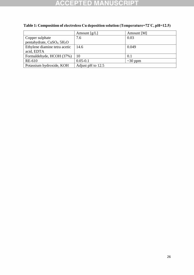
The composition of Cu ELD solution is presented in Table 1. Au nanostructure modified Ppy
electrodes were dipped in the Cu ELD bath maintained at a temperature of 72˚C for different
times. The AuNP(E)/Ppy was coated by Cu for 90, 120, 300 ,420 and 540 s whereas, Au923
(M)/ Ppy was coated for 50, 90,120, 420 and 540 s. After ELD the samples were washed
thoroughly in DI water, and then dried with N2 flow.
2.2 Characterization
The AuNP(E) electroplated on Ppy as well as the nucleation and Cu film growth were studied
by Quanta 200 FEG Environmental Scanning Electron Microscope (ESEM). Whereas,
Au923(M) cluster were deposited on Cu grids coated by Ppy and were imaged by a JEOL
JEM2100F STEM with a CEOS Cs-corrector[28]. The particle size and particle number in both
the cases was evaluated by the image processing with ImageJ (NIH) software[26].
The Cu content (Wt%) in the samples was detected by Energy dispersive X-ray spectroscopy.
Surface morphology and roughness were investigated by Atomic force microscopy (AFM
MI150) in tapping mode for 20x20µm. X-ray reflection fluorimeter (Fischerscope® X-Ray
XAN®-FD) was used to measure the Cu film thickness. The XRF was calibrated for “Cu films
on plastic substrate” module was used for all the measurements.
3. Results and Discussion
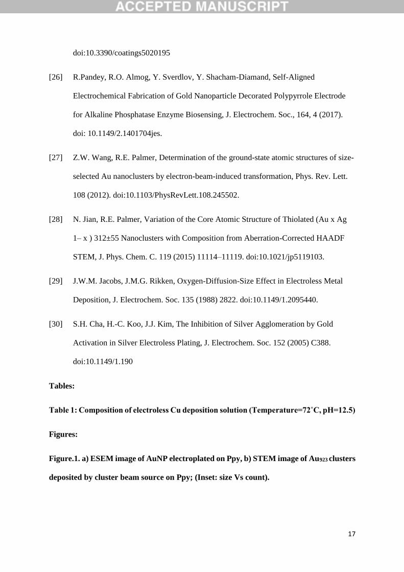
ESEM image of electroplated AuNP(E) on polypyrrole is presented in Fig.1a. Sparsely
distributed AuNP(E) can be seen all over the Ppy. The inset in Fig. 1a shows that the particles
7
have a wide size distribution. The average size of the nanoparticles was found to be 50±5 nm
(inset Fig.1.a). A HAADF-STEM image of the Au923(M) clusters is shown in Fig.1b. In contrast
to AuNP(E), the clusters of uniform size of 6±0.5 nm (inset Fig.1b) are uniformly distributed
on the Ppy surface. The calculated number of particle was found to be 2200/cm2 and 3x 10¹²
/cm2 for AuNP(E) and Au923(M), respectively. This huge difference in the surface area
contributes in the improved catalysis of Cu film formation by Au923(M) as shown later in this
work.
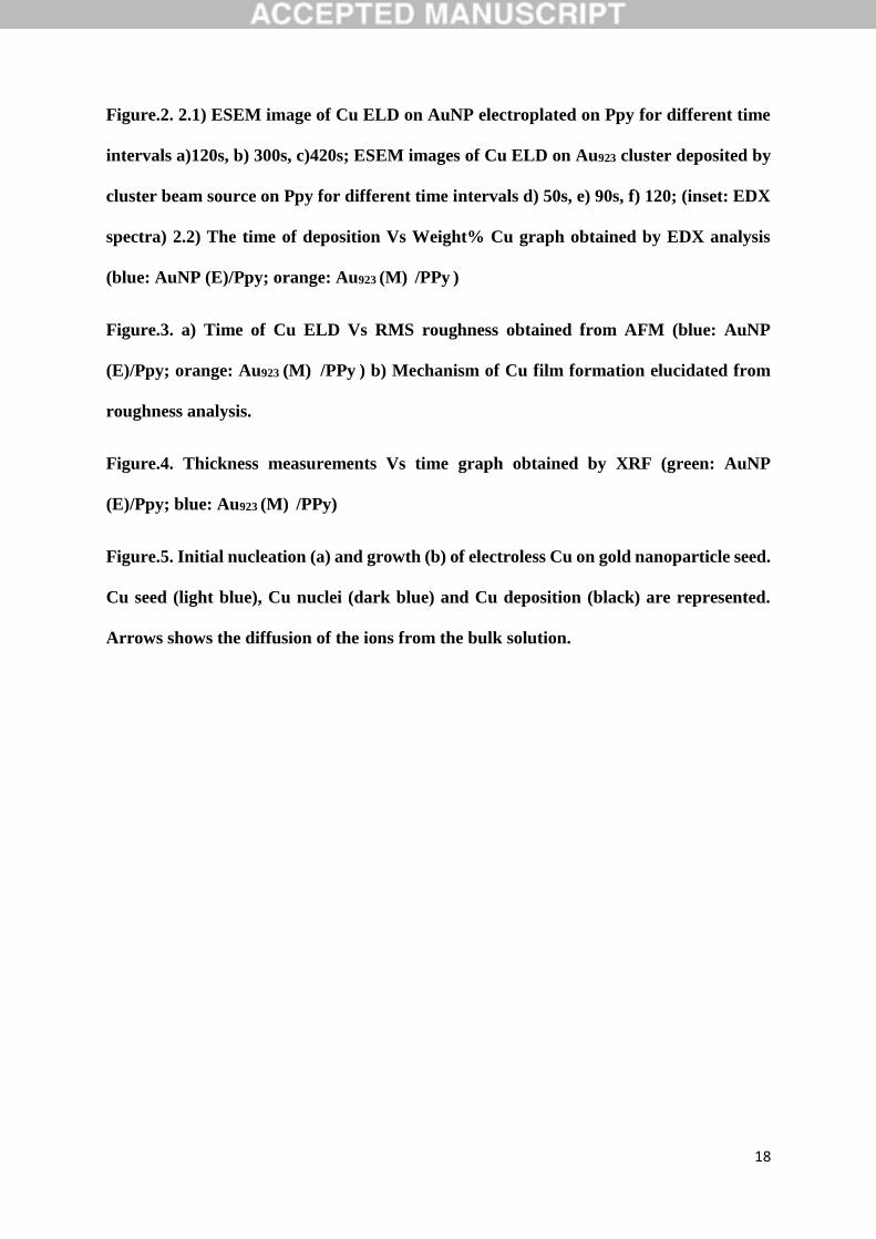
The morphology of the Ppy surface after Cu ELD is presented in Fig. 2.1. Formation of Cu/Au
NPs on the electroplated AuNP(E) surface after 120 s of Cu electroless deposition was
observed (Fig. 2.1a.). While after 300 s of ELD the Cu islands appears due to coalescence of
the various nearby Cu/Au NPs (Fig. 2.1b). Further, Cu film growth (420 s) allows formation
of Cu film with very globular morphology (Fig. 2.1c). For Ppy activated by Au923(M) cluster,
continuous Cu layer was observed on the surface after very short time of ELD (Fig. 2.1d). It
indicates formation of smooth thin film right after 120 s of deposition (Figs. 2.1e,f). In both
cases a gradual increase followed by saturation of the Cu content on the substrate is observed
with the increase in deposition time (Fig. 2.2). The incubation time can be roughly estimated
to be less than 90s; however, more comprehensive study of incubation time is performed by
XRF later in the paper.
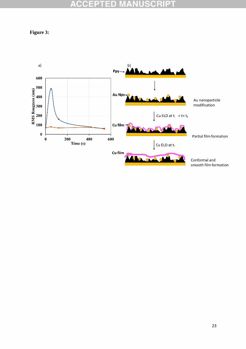
The dependence of Cu film surface roughness (RMS) on the time of its deposition is shown in
Fig. 3. Two different trends were observed in the RMS vs time graph. In the case of the
AuNP(E), there is a sudden increase in the roughness in 50 s then a gradual decrease in the
roughness w.r.t. time. Similar increase is seen in Au923 (M) at 50 s, however, it’s less compared
to the former case. This could be since the AuNPs(E) are almost ten times bigger than the
Au923NP(M) and hence it gives rise to a very uneven and rough surface. With the course of
8
time the roughness decreases slowly and reaches a constant value around 500 s for both cases
(Fig. 3a). The roughness increases with the time (t)
𝑡𝑖 < 𝑡 < 𝑡𝑓 (1)
Where, ti and tf are initial and final time of deposition (Fig. 3b). At tf , the roughness reduces
rapidly giving a smooth and shiny Cu coverage.
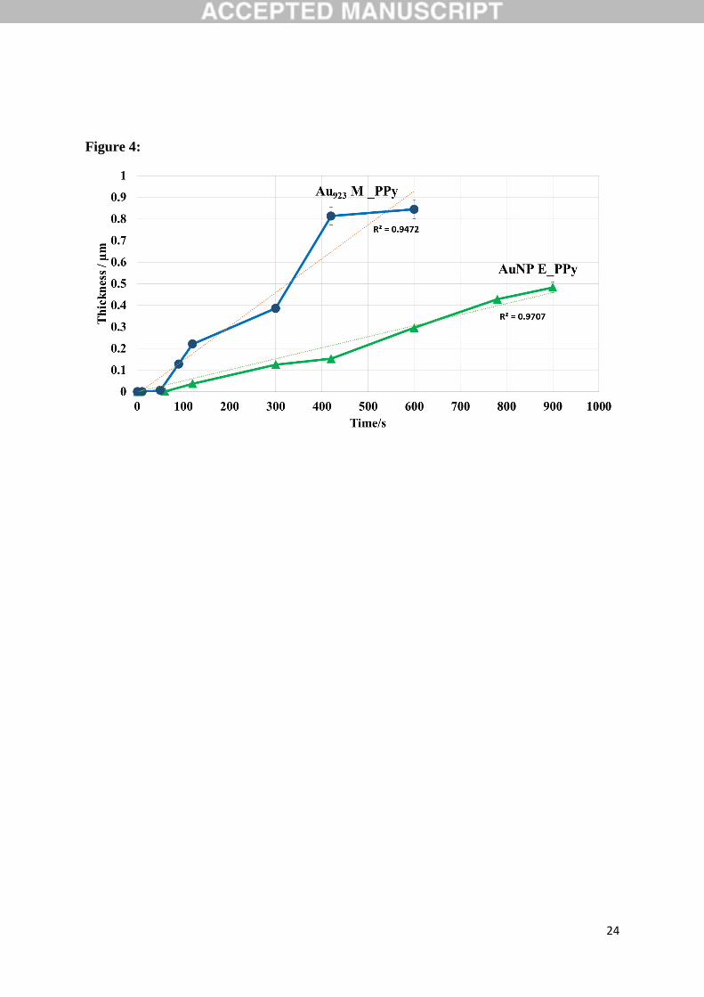
Fig. 4 depicts the relationship of Cu film thickness measured at different time of deposition
obtained by XRF. The linear dependence of the Cu film thickness on the deposition time was
observed for AuNP (E)/Ppy substrate when compared to Au923 (M)/Ppy. The calculated
deposition rate of Cu on AuNP (E)/Ppy was found to be 20 nm/min (calculated from the slope
of the best fitted linear region of the thickness vs time graph), which is slower than that on
Au923 (M)/Ppy (85 nm/min). This demonstrates that Au923 (M) is the better catalyst for the Cu
film growth than AuNP (E). Such effect may be explained by high purity, high surface density,
high size uniformity and homogeneous distribution of Au923 (M) clusters on the Ppy compared
to AuNP (E) one. The growth trend also seems to be very gentle in case of AuNP (E)/Ppy when
compared to steep growth in Au923(M)/Ppy.
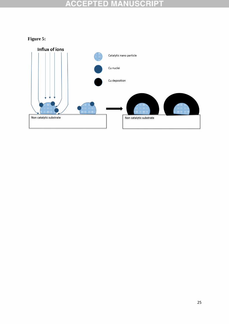
In both cases, the deposition is initiated on the surface of the nanoscale catalytic metal. Note,
that the incubation time is similar in both cases. Incubation can be due to various reasons, one
of them is due to the nucleation time where classical models assume that it depends on the
binding energy between the catalytic surface (gold in our cases) and the deposited metal (Cu
for both) (Fig. 5). The film continues to grow laterally between the nanoparticles until almost
full coverage is achieved. Once the surface is fully covered the thin film continues to grow
vertically. For nanoparticle seeding the initial stage includes two parts (Fig. 5):
1. Nucleation of copper on the catalytic metal nanoparticles until reaching full coverage on the
nanoparticle.
2. Lateral growth between the nanoparticles until coalescence.
9
Conventional models of nucleation in electroless deposition assumes an effective energy
barrier E*, that depends on the reduction in the free energy during crystallization and the
increase in the surface energy. This model is only an approximation since in our case the
substrate is non-flat and the dimension of the critical nucleus is not much smaller than the
catalytic nanoparticles size. The critical nucleus assuming an ideal spherical symmetry is given
by [14]:
𝑟∗ =2𝛾𝜐
[𝑛𝐹(𝐸𝑚𝑒−𝐸𝑟𝑒𝑑)] (2)
Where, γ is the surface tension, 𝜐 is the molar volume of the metal deposit, n is the number of
electrons involved in the redox reaction, F is the Faraday constant, and (Eme - Ered) is the
potential between the metal (Cu) deposited and the reducing agent. Calculating this critical
value for the basic electroless deposition solution (Table 1) yields a value of about 0.3 nm [14].
Therefore, we can assume that the critical radius of nucleation is significantly smaller than the
nanoparticles used in this work as nucleation centers and that the initial nucleation step occurs
on the gold nanoparticles until coalescence is partial or complete. This is followed by lateral
and vertical growth of copper islands. This happens until the gap between the initial
nanoparticles is completely filled with electroless deposition, the lateral deposition stops and
the growth becomes only in the vertical dimension.
Once nucleation occurs the deposition rate for basic electroless Cu deposition is assumed to be
a function of four parameters: (a) the copper complex concentration, CCu-complex, (b) the
reducing agent (Formaldehyde in our case) concentration CHCOH, (c) the hydroxyl ion
concentration OH- and (d) the complexing agent (Ligand) concentration (e.g. EDTA):
𝑅 = 𝐾 ∙ 𝐶Cu−complex𝑎 ∙ 𝐶𝐻𝐶𝑂𝐻
𝑏 ∙ 𝐶𝑂𝐻−𝑐 ∙ 𝐶𝐸𝐷𝑇𝐴4−
𝑑 (3)
The various constants a, b, c, d, are presented for the steady state in the literature for few cases
[14]. There is no data regarding the dependence of the deposition rate during the transient on
10
the various concentrations at the electrode interface. In the text presented here we will assume
that the main dependence of the deposition rate is on the concentration of the copper metal
ions. This is an approximation that needs to be re-examined in the future. Next, we will take
into consideration of the formaldehyde concentration. The treatment here is qualitative and a
full numerical analysis of the system may shed more light on the actual kinetics of the initial
stage of the surface coverage. The solution to the diffusion equation assuming a diffusion
coefficient DCu of the Cu ions and surface reaction constant ks can be estimated from the
deposition rate at period past the initial incubation period where the deposition rate is constant.
This is typically at times longer than 2 minutes. At much longer time the deposition rate starts
to drop, typically after 20-25 minutes in conventional open bath at the 70-75˚C range, without
agitation. The reaction constant can be estimated using the relation between the deposition rate
and the flux of Cu ions towards the surface:
𝐹𝑙𝑢𝑥 =𝑅∙𝜌∙𝑁𝐴
𝑀𝑊 (4)
Where, ρ is the metal density [g/cm3], MW is the molecular weights [g/mole] and NA is the
Avogadro number. Assuming that the deposition rate depends only on the metal ion (Cu)
concentration:
𝑅 [𝑐𝑚
𝑠𝑒𝑐] = 𝑅′ ∙ [𝐶𝑢] [
𝑚𝑜𝑙𝑒
𝐿] = 𝑅′ ∙ 103[𝐶𝑢] [
𝑚𝑜𝑙𝑒
𝑐𝑐]
=𝑅′ ∙ 103[𝐶𝑢]
𝑁𝐴∙ [𝐶𝑢] [
# 𝑚𝑜𝑙𝑒𝑐𝑢𝑙𝑒𝑠
𝑐𝑐 𝑜𝑟 𝑐𝑚−3]
(5)
This can be written as:
𝐹𝑙𝑢𝑥 =𝑅′∙103∙𝜌
𝑀𝑊∙ [𝐶𝑢] = 𝑘𝑠 ∙ [𝐶𝑢] or 𝑘𝑠 =
𝑅′∙103∙𝜌
𝑀𝑊 (6)
Where, R’ is the deposition rate divided by the Cu concertation near the electrode. The constant
ks has units of velocity [cm/s] and can be referred to as the surface reaction velocity.
11
Assuming a deposition rate of 14.16x10⁻⁸cm/s for the Au923(M) and 3.36x10⁻⁸cm/s for the
AuNPs(E) (Fig.4, given MW=63.546 g/mole and density of 8.92 g/cm3 of Cu , the effective
surface reaction velocity is 18.5x10⁻⁵ cm/s for the AuNPs(E) and 79.9x10⁻⁵ cm/s for the
Au923(M). A higher surface area in the case of Au923(M) corresponds to higher surface reaction
velocity as well as deposition rate when compared to AuNPs(E).
Solving the electroless deposition in one dimension, assuming the deposition rate depends only
on the Cu concentration is given by[22]:
𝐽 = 𝑞 ∙ 𝑛 ∙ 𝑘𝑠 ∙ 𝑐(𝑥, 0) ∙ exp (𝑘𝑠
2⋅𝑡
𝐷) ⋅ 𝑒𝑟𝑓𝑐 (
𝑘𝑠⋅√𝑡
√𝐷) (7)
Where D is diffusion coefficient of Cu ion, n is the number of electrons involved in the Cu ion
reduction (n=2), c(x,0)=CCu (0) is the initial Cu concentration in the bath and ks is the surface
reaction velocity of the equation CCu --> CCu2+. We can define a critical time:
𝑡𝑐 =𝐷
𝑘𝑠2 (8)
At very short time, t << tc , the expressions is time independent:
𝐽 = 𝑞 ∙ 𝑛 ∙ 𝑘𝑠 ∙ 𝑐(𝑥, 0) (9)
While for long time, t >> tc, we get
𝐽 =𝑞∙𝑛∙𝑘𝑠∙𝑐(𝑥,0)
√𝜋𝐷𝑡 (10)
This model can be extended for non-flat surface, specifically for hemi- spherical nuclei.
Applying it to 2D and 3D yields a solution where the current at long time is not zero but reaches
a value that actually depends on the radius of the spherical nuclei acting as an electrode. This
yields an initial high deposition rate for the smaller particle in comparison to the larger nano
particles. Therefore, we may assume that once Cu nano particle has been formed on the Au
nanoparticle the nuclei on the smaller nano particles grow rapidly so the overall lateral growth
is similar for both small and larger nanoparticles. Assuming D= 7x10⁻⁶ cm2 /s for the Cu ion in
the solution (in the complex form), the critical time for moving from surface reaction limited
12
regime to diffusion limited regime is in the range of several minutes to hours, thus we can
conclude that at the initial deposition, the nucleation and growth is mostly surface reaction
limited. Note that the numerical solution presented in [23] indicates that the surface reaction
drops instantly at the initial stage of deposition but consecutively drops at a slow rate yielding
almost constant deposition rate up to t >1000 s of deposition.
As stated before, the incubation time is very similar in both cases. Jacobs et.al [29] reported
that small size particles retards the deposition due to nonlinear diffusion effect of dissolved
oxygen towards smaller feature. The incubation time is also a function of binding energy of the
substrate and the deposited metal and the crystallographic misfit between them[30]. The Au
and Cu have same crystal structure (fcc) and the value of the lattice constant is more or less
similar in both Au923(M) clusters and AuNP(E). The binding energy of Cu-Au is also very
similar in both the case. However, it could also be possible that the initial growth of the Cu on
Au923(M) is very fast which balances the slow growth of the Cu on AuNPs(E) until they
coalescence and a film is formed.
4. Conclusion
A novel method of polypyrrole film metallization was studied. The Ppy surface was activated
by two different Au nanostructures, electrodeposited AuNPs and Au923 clusters, before Cu
electroless deposition. It was shown that the Cu film deposition rate depended on the substrate
activation procedure. The copper deposition rate on the Au923(M)/Ppy surface was at least three
times higher than that on AuNP(E)/Ppy. It was understood in terms of the surface reaction
velocity, which was found higher for small size and higher surface area, Au923(M)/PPy sample.
This behavior was explained by the small size of Au923(M) catalyst features and their uniform
distribution on the substrate. The copper film roughness as a function of its thickness was
studied. Smoothening of the film with an increase in the Cu film thickness was observed. Two
different trends in the roughness transformation during film growth demonstrate the extent of
13
influence of the catalytic surface texture and its nanostructure size on Cu ELD film. There are
two possible mechanisms for the nucleation behavior that is observed and explained
qualitatively in this work:
a. Effect of free energy of formation of the Cu deposition on the Au nanoparticles on
incubation time.
b. The lateral growth of Cu between the nanoparticles after nucleation and growth of Cu on
the Au nano particles themselves.
Once nucleation is reached, the deposition rate is rather constant. It should be noted that very
similar incubation times for copper electroless deposition on both the Au923(M)/Ppy and
AuNP(E)/Ppy surfaces were observed. It was shown that the incubation time is not dependent
on the size of the catalyst Au, but on various other factors like catalytic surface- deposited
metal binding energy (Cu-Au), and their lattice parameters. Moreover, the incubation is also
determined by the nature of the bath. This study provides groundwork on the effect of Au
activation seed parameters on the Cu electroless deposition on polypyrrole.
Acknowledgments
The research leading to these results has received funding from the European Union's Seventh
Framework Programme (FP7/2007-2013) under grant agreement no. 607417 (CATSENSE).
The cluster beam deposition and STEM work were also supported by the Birmingham Science
City project and EPSRC. We are grateful to Mr. Omri Heifler from Tel Aviv University
Nanocentre and Oleg Kovalenko from Technion-Israel Institute of Technology for their efforts
in acquiring the AFM results and to Ms. Stav Friedberg and Mr. Avi Yaverboim for the XRF
measurements.
14
References
[1] G.E. Moore, Cramming more components onto integrated circuits (Reprinted from
Electronics, pg 114-117, April 19, 1965), Proc. Ieee. 86 (1998) 82–85. doi:10.1109/N-
SSC.2006.4785860.
[2] R.G. Arns, The other transistor: early history of the metal-oxide semiconductor field-
effect transistor, Eng. Sci. Educ. J. 7 (1998) 233–240. doi:10.1049/esej:19980509.
[3] E. Vogel, Technology and metrology of new electronic materials and devices., Nat.
Nanotechnol. 2 (2007) 25–32. doi:10.1038/nnano.2006.142.
[4] D.-H. Kim, R. Ghaffari, N. Lu, J. A Rogers, Flexible and stretchable electronics for
biointegrated devices., Annu. Rev. Biomed. Eng. 14 (2012) 113–28.
doi:10.1146/annurev-bioeng-071811-150018.
[5] M. Gerard, A. Chaubey, B.D. Malhotra, Application of conducting polymers to
biosensors, Biosens. Bioelectron. 17 (2002) 345–359. doi:10.1016/S0956-
5663(01)00312-8.
[6] A.G. MacDiarmid, Polyaniline and polypyrrole: Where are we headed?, Synth. Met.
84 (1997) 27–34. doi:10.1016/S0379-6779(97)80658-3.
[7] I. Dodouche, F. Epron, Promoting effect of electroactive polymer supports on the
catalytic performances of palladium-based catalysts for nitrite reduction in water,
Appl. Catal. B Environ. 76 (2007) 291–299. doi:10.1016/j.apcatb.2007.06.002.
[8] L. Torsi, M. Pezzuto, P. Siciliano, R. Rella, L. Sabbatini, L. Valli, P.. Zambonin,
Conducting polymers doped with metallic inclusions: New materials for gas sensors,
Sensors Actuators B Chem. 48 (1998) 362–367. doi:10.1016/S0925-4005(98)00058-
6.
15
[9] V. Zaporojtchenko, T. Strunskus, K. Behnke, C. V. Bechtolsheim, A. Thran, F.
Faupel, Formation of metal-polymer interfaces by metal evaporation: Influence of
deposition parameters and defects, Microelectron. Eng. 50 (2000) 465–471.
doi:10.1016/S0167-9317(99)00316-0.
[10] R.W. Burger, L.J. Gerenser, Metallized Plastics 3 : Fundamental and Applied Aspects,
1992. doi:10.1007/978-1-4615-3416-7.
[11] V.W.L. Lim, E.T. Kang, K.G. Neoh, Electroless plating of palladium and copper on
polypyrrole films, Synth. Met. 123 (2001) 107–115. doi:10.1016/S0379-
6779(00)00592-0.
[12] Y. Ohnishi, S. Yoshimoto, M. Kato, Metal pattern formation by selective electroless
metallization on polypyrrole films patterned by photochemical degradation of iron(III)
chloride as oxidizing agent, Synth. Met. 144 (2004) 265–269.
doi:10.1016/j.synthmet.2004.04.015.
[13] S. Schaefers, L. Rast, A. Stanishevsky, Electroless silver plating on spin-coated silver
nanoparticle seed layers, 2006. doi:10.1016/j.matlet.2005.05.085.
[14] Y. Shacham-Diamand, V. Dubin, M. Angyal, Electroless copper deposition for ULSI,
Thin Solid Films. 262 (1995) 93–103. doi:10.1016/0040-6090(95)05836-2.
[15] F. Yin, Z.W. Wang, R.E. Palmer, Controlled formation of mass-selected Cu-Au core-
shell cluster beams, J. Am. Chem. Soc. 133 (2011) 10325–10327.
doi:10.1021/ja201218n.
[16] S.R. Plant, L. Cao, R.E. Palmer, Atomic structure control of size-selected gold
nanoclusters during formation, J. Am. Chem. Soc. 136 (2014) 7559–7562.
doi:10.1021/ja502769v.
16
[17] D.M. Wells, G. Rossi, R. Ferrando, R.E. Palmer, Metastability of the atomic
structures of size-selected gold nanoparticles, Nanoscale. 7 (2015) 6498–6503.
doi:10.1039/C4NR05811A.
[18] S. Pratontep, S.J. Carroll, C. Xirouchaki, M. Streun, R.E. Palmer, Size-selected cluster
beam source based on radio frequency magnetron plasma sputtering and gas
condensation, Rev. Sci. Instrum. 76 (2005). doi:10.1063/1.1869332.
[19] M. Paunovic and C. H. Ting, in Electroless Deposition of Metals and Alloys,M.
Paunovic and I. Ohno, Eds., Proceedings, Vol. 12, Electrochemical Society,
Pennington, NJ, 1988, p. 170. doi: 10.1007/978-1-4615-9576-2_30
[20] M. Paunovic and C. Stack, in Electrocrystallization, R. Weil and R, G. Barad as, Eds.,
Proceedings, Vol. 6, Electrochemical Society, Pennington, NJ, 1981, p. 205.
[21] R. Sard, The Nucleation, Growth, and Structure of Electroless Copper Deposits, J.
Electrochem. Soc., 117, 864 (1970). doi: 10.1149/1.2407658.
[22] M. Paunovic, Electroless deposition of copper, in Modern Electroplating, Fifth Edition
Edited by Mordechay Schlesinger and Milan Paunovic, pp. 433-446. John Wiley &
Sons, Inc. (2010)
[23] G.Hills, A.K.Pour, B.Scharifker. The formation and properties of single nuclei.
Electrochimica Acta, 28 (1983), 891-898. doi: 10.1016/0013-4686(83)85164-0
[24] M. Ramasubramanian, B. N.Popov, R. E.White, K. S.Chen, A mathematical model for
electroless copper deposition on planar substrates. J. Electrochem. Soc., 146 (1999),
111-116. doi: 10.1149/1.1391572
[25] G. Zangari, Electrodeposition of Alloys and Compounds in the Era of Microelectronics
and Energy Conversion Technology, Coatings 2015, 5, 195-218;
17
doi:10.3390/coatings5020195
[26] R.Pandey, R.O. Almog, Y. Sverdlov, Y. Shacham-Diamand, Self-Aligned
Electrochemical Fabrication of Gold Nanoparticle Decorated Polypyrrole Electrode
for Alkaline Phosphatase Enzyme Biosensing, J. Electrochem. Soc., 164, 4 (2017).
doi: 10.1149/2.1401704jes.
[27] Z.W. Wang, R.E. Palmer, Determination of the ground-state atomic structures of size-
selected Au nanoclusters by electron-beam-induced transformation, Phys. Rev. Lett.
108 (2012). doi:10.1103/PhysRevLett.108.245502.
[28] N. Jian, R.E. Palmer, Variation of the Core Atomic Structure of Thiolated (Au x Ag
1– x ) 312±55 Nanoclusters with Composition from Aberration-Corrected HAADF
STEM, J. Phys. Chem. C. 119 (2015) 11114–11119. doi:10.1021/jp5119103.
[29] J.W.M. Jacobs, J.M.G. Rikken, Oxygen-Diffusion-Size Effect in Electroless Metal
Deposition, J. Electrochem. Soc. 135 (1988) 2822. doi:10.1149/1.2095440.
[30] S.H. Cha, H.-C. Koo, J.J. Kim, The Inhibition of Silver Agglomeration by Gold
Activation in Silver Electroless Plating, J. Electrochem. Soc. 152 (2005) C388.
doi:10.1149/1.190
Tables:
Table 1: Composition of electroless Cu deposition solution (Temperature=72˚C, pH=12.5)
Figures:
Figure.1. a) ESEM image of AuNP electroplated on Ppy, b) STEM image of Au923 clusters
deposited by cluster beam source on Ppy; (Inset: size Vs count).
18
Figure.2. 2.1) ESEM image of Cu ELD on AuNP electroplated on Ppy for different time
intervals a)120s, b) 300s, c)420s; ESEM images of Cu ELD on Au923 cluster deposited by
cluster beam source on Ppy for different time intervals d) 50s, e) 90s, f) 120; (inset: EDX
spectra) 2.2) The time of deposition Vs Weight% Cu graph obtained by EDX analysis
(blue: AuNP (E)/Ppy; orange: Au923 (M) /PPy )
Figure.3. a) Time of Cu ELD Vs RMS roughness obtained from AFM (blue: AuNP
(E)/Ppy; orange: Au923 (M) /PPy ) b) Mechanism of Cu film formation elucidated from
roughness analysis.
Figure.4. Thickness measurements Vs time graph obtained by XRF (green: AuNP
(E)/Ppy; blue: Au923 (M) /PPy)
Figure.5. Initial nucleation (a) and growth (b) of electroless Cu on gold nanoparticle seed.
Cu seed (light blue), Cu nuclei (dark blue) and Cu deposition (black) are represented.
Arrows shows the diffusion of the ions from the bulk solution.

19

20
21
Figr-1Figure 1:
22
Figure 2:
23
Figure 3:
24
Figure 4:
25
Figure 5:
26
Table 1: Composition of electroless Cu deposition solution (Temperature=72˚C, pH=12.5)
Amount [g/L] Amount [M]
Copper sulphate
pentahydrate, CuSO4. 5H2O
7.6 0.03
Ethylene diamine tetra acetic
acid, EDTA
14.6 0.049
Formaldehyde, HCOH (37%) 10 0.1
RE-610 0.05-0.1 ~30 ppm
Potassium hydroxide, KOH Adjust pH to 12.5