Embed Size (px)
Citation preview
MEMS MATERIALS AND PROCESSES: a research overview
S. Mark Spearing
Department of Aeronautics and Astronautics Massachusetts Institute of Technology
Abstract—An overview is provided of materials and processes research currently being conducted in support of MEMS device design at MIT. Underpinning research is being conducted in five areas: room temperature strength characterization, elevated temperature strength characterization, processing of Si/SiC hybrid structures, modeling of wafer bonding processes and development of high temperature fluid interconnections. Emphasis is placed on the key areas of materials science and engineering.
Index Terms—Microelectromechanical systems, Mechanical properties, process development, process modeling.
I. INTRODUCTION
MICROELECTROMECHANICAL SYSTEMS (MEMS) is an area of technology of rapidly increasing economic
importance. Commercial devices include accelerometers, pressure sensors, ink jet printer heads, digital mirror arrays for projectors and atomic force microscopes. The total global market value is currently in the range US$2-4 billion. Significant growth is anticipated, particularly in the areas of biological devices, optical switching, radio-frequency switching and in compact high power-density actuators and power generation systems. The ability to develop viable MEMS in these new areas is to a large degree enabled and constrained by the set of materials and processes from which a designer can select. Hitherto the vast majority of commercial MEMS have utilized the CMOS/VLSI materials and process set. However, this is not sufficient, particularly as higher power levels and operating temperatures are desired.
Several projects are under way at MIT to develop high-power density MEMS for the generation of portable electrical power. These include the Microengine, Micro-hydraulic Transducer and Micro-chemical Power programs. These projects use very different approaches to generate electrical power from microfabricated devices. However, the goal of high power levels translates to a common set of requirements for materials and processes. In particular the following areas have been found to be of prime importance: characterization and modeling of the room temperature strength of silicion and the development of processes to control it, characterization and modeling of the elevated temperature strength of silicon, development of thick film techniques for refractory materials, development of wafer bonding techniques for multi-wafer
stacks and the development of packaging strategies to provide fluid-interconnections to and from the MEMS device. In addition other specific materials and process issues also arise, but these are not the focus of this paper. Each of the key cross-cutting topics is briefly overviewed in this paper, and references to more complete descriptions are provided.
II. ROOM TEMPERATURE STRENGTH OF SILICON At room temperature silicon is a brittle material and is
therefore expected to exhibit to exhibit a statistical scaling of strength which obeys weakest link statistics. In addition the strength is expected to be very sensitive to the local surface roughness, which in turn is expected to be sensitive to the etch conditions used to create the structure. This implies that the mechanical testing of silicon must employ a statistically significant number of test specimens fabricated using the same etch method as is to be used for the target devices in order to yield valid data. Furthermore, it is anticipated that structural design methods will need to account for the scatter in the achievable strength and the scaling due to the volume (or surface area) under stress.
In order to account for these factors a two-part approach has been used to characterize and to model the strength of silicon. A) a simple mechanical testing procedure has been developed and B) a probabilistic design software package has been employed to translate the mechanical test data into structural analysis.
A. Mechanical Testing A biaxial testing configuration is the preferred method used
to characterize the strength of silicon specimens [1]. Specimens are supported over a circular hole and are then loaded centrally. Loading is achieved by either a modified micro-hardness indentor or a purpose-built loading jig, which uses a piezo-stack to achieve precise control of the indentor position. In both cases the applied load is recorded by a load cell mounted under the specimen support. Two test specimen configurations have been employed, a) a flat specimen or b) a "radius-hub flexure specimen. The latter specimen configuration allows a local determination of the effective strength at the bottom of deep etch trenches or at the edge of thin membranes.
The data is reduced according to the Weibull probability

density function, which can be expressed in the form given below, giving the probability of failure of a volume of material, V, at a stress σ:
Pf (σ ,V ) = 1 − exp(−VV0
(σσ0
)m ) (1)
Where V0, at a stress σ0 are reference values of the volume
and stress respectively and m is the Weibull modulus, which provides a measure of the scatter in the data. The same basic equation can be used for cases in which the failure is dominated by a surface flaw distribution, in which case the areas are substituted for volumes. This latter case is more appropriate for single crystal silicon, which is free of bulk mechanical defects.
Typical data is obtained of the form shown in figure 1. The data is reduced by plotting (ln[strength] vs. ln[ln[1-Pf]], which yields a straight line for samples of data obeying equation (1). As can be seen from figure 1, the strength is found to be a strong function of the etch conditions [2. The data is also found to vary locally, with low strengths corresponding to the rough regions found at the fillet radii at the bottom of deep etched trenches or the edges of membrane structures. These low strengths correlate directly to the increased roughness observed in these regions, as shown in figure 2.
Fig. 1. Weibull plot of strength vs probability of failure for deep etched
silicon radius hub flexure specimens. The specimens were prepared by several etch recipes. The effect of secondary isotropic SF6 etches are shown. The capability to increase the strength by reducing the severity of surface defects is clearly demonstrated.
B. Probabilistic Design/Analysis NASA's CARES software has been employed to translate
the mechanical test data into a form usable in structural design/analysis. The software fits a Weibull probability density function to the test data and then applies it through a post-processor to a finite element model of the structure to be analyzed. CARES uses the principal of independent action to separately calculate the probability of failure due to each principal stress component in the area of material associated with each integration point. The probability of failure for the
entire structure is then obtained by multiplying the probabilities of failure for the individual integration points [3].
Results such as those shown in figure 1 indicate that a Weibull probability density function is a reasonable fit to individual data sets. However, as yet, there has been less success in predicting the failure of more complicated structures based on the data obtained from the strength tests on relatively simple mechanical tests specimens. This is attributed to local variations in the surface roughness achieved by the etching in the structures that are not achieved when fabricating the test specimens, as shown in figure 2. This finding suggests that more attention must be given to choosing representative mechanical test structures, that not only replicate the stress states experienced in the real devices, but also yield representative local etch conditions. Until a better approach is identified, MEMS structural design against failure has to err on the overly conservative side.
Fig. 2. Shows a typical deep etched silicon surface and the transition to a horizontal surface. The surface roughness is a major contribution to the strength-controlling flaw population
III. HIGH TEMPERATURE STRENGTH OF SILICON
Devices such as the microengine, micro-rocket and micro-chemical power system require operation at elevated temperatures. They also require relatively high stress levels. This implies that to design successful devices an adequate constitutive model, that includes the effect of temperatures and loading rates, for the materials under consideration must be available. Silicon is the primary structural material for all of these devices, but prior to the inception of these devices there was no pre-existing materials model adequate for device design. Over the past three years a model has been developed, validated and applied to the design of silicon devices [4,5]. The model uses a standard continuum plasticity framework, in
which dislocation motion is the primary deformation mechanism. Based on literature data the elevated response of silicion is divided into two regimes, corresponding to low and high dislocation densities. At low dislocation densities, dislocation nucleation is the rate limiting process and a nominal dislocation density is used as the internal state variable. At high dislocation densities dislocation interactions are the rate limiting process and a nominal internal shear resistance is used as the state variable. A convenient fitting function is used to create a smooth transition between the regimes. In addition simple, empirically-determined functions are used to describe the evolution of dislocation density and the internal shear resistance in terms of the current deformation state, stress and temperature.
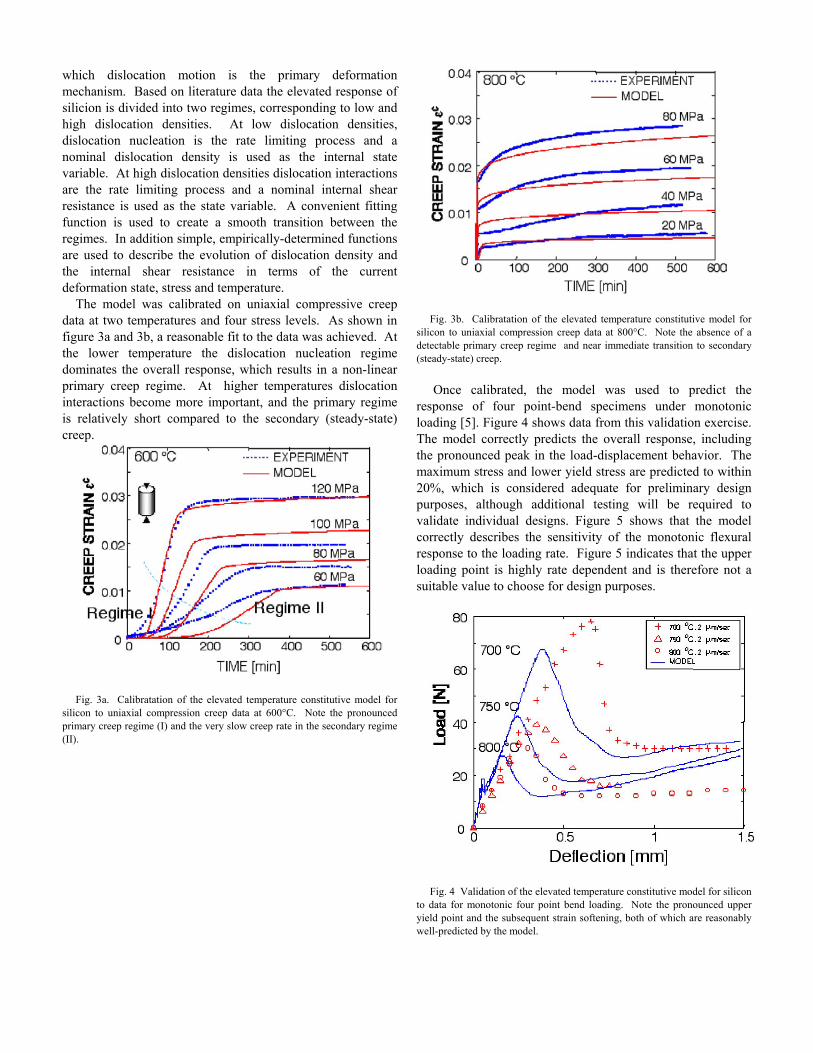
The model was calibrated on uniaxial compressive creep data at two temperatures and four stress levels. As shown in figure 3a and 3b, a reasonable fit to the data was achieved. At the lower temperature the dislocation nucleation regime dominates the overall response, which results in a non-linear primary creep regime. At higher temperatures dislocation interactions become more important, and the primary regime is relatively short compared to the secondary (steady-state) creep.
Fig. 3a. Calibratation of the elevated temperature constitutive model for
silicon to uniaxial compression creep data at 600°C. Note the pronounced primary creep regime (I) and the very slow creep rate in the secondary regime (II).
Fig. 3b. Calibratation of the elevated temperature constitutive model for
silicon to uniaxial compression creep data at 800°C. Note the absence of a detectable primary creep regime and near immediate transition to secondary (steady-state) creep.
Once calibrated, the model was used to predict the
response of four point-bend specimens under monotonic loading [5]. Figure 4 shows data from this validation exercise. The model correctly predicts the overall response, including the pronounced peak in the load-displacement behavior. The maximum stress and lower yield stress are predicted to within 20%, which is considered adequate for preliminary design purposes, although additional testing will be required to validate individual designs. Figure 5 shows that the model correctly describes the sensitivity of the monotonic flexural response to the loading rate. Figure 5 indicates that the upper loading point is highly rate dependent and is therefore not a suitable value to choose for design purposes.
Fig. 4 Validation of the elevated temperature constitutive model for silicon
to data for monotonic four point bend loading. Note the pronounced upper yield point and the subsequent strain softening, both of which are reasonably well-predicted by the model.

Fig. 5 Validation of the elevated temperature constitutive model for silicon
to data for monotonic four point bend loading at two different loading points. Note the strong dependence of the yield point on the loading rate, an effect that is adequately captured by the model.
Additional validation of the constitutive model was
achieved on Si/SiC hybrid specimens, consisting of four-point bend specimens with chemical vapor deposited SiC layers, 30µm thick on the top and bottom surfaces. SiC is very refractory and behaves elastically at temperatures well above the softening point of silicon. Combining the silicon constitutive model with the elastic response of SiC, allowed a good prediction of the flexural response of the hybrid specimens, as shown in figure 6. An accurate prediction of the load-deflection response was achieved by the model. It is interesting to note that the ultimate failure load at 900°C is approximately six times the upper yield stress of monolithic silicon at this temperature. It is also important to note that when fracture occurred, predominantly in the silicon, the SiC remained bonded to the silicon, indicating that the Si-SiC bond is robust, even at high temperatures. Furthermore, additional strengthening could be achieved if higher strength SiC could be fabricated. The concept of using SiC reinforcement for silicon structures is being actively pursued for several of the aforementioned MEMS devices [6], the next section describes the development of the processes required to achieve such structures.
Fig. 6 Validation of the elevated temperature constitutive model for silicon
to data for monotonic four point bend loading for Si/SiC hybrid specimens. 30 µm thick SiC films were deposited on the outer ligaments of the specimen. Note the dramatic reinforcement beyond the initial silicon yield point, particularly at 900°C.
IV. PROCESSING OF THICK REFRACTORY FILMS The demonstration that the operating temperature of silicon
MEMS can be extended by the use of local reinforcement with refractory materials is very exciting. Materials such as SiC are difficult to etch or shape with the precision required of most MEMS devices. However, if it is only required to place SiC within the bulk of the structure, it is possible to achieve all the features requiring fine tolerances in Si, for which processing techniques are well developed. The approach we are developing consists of four key steps [7,8]: 1) a silicon wafer is etched to create open cavities. 2) the entire wafer is over-deposited with a thick (10-100 µm) of SiC. 3) The overburden of SiC is removed by grinding and polishing to yield a flat wafer with the cavities filled with SiC. 4) The wafer containing the SiC reinforcement is then bonded to a second Si wafer. This two wafer stack enters the remainder of the process and is treated as though it were a standard Si wafer. Careful registration is maintained to ensure that the SiC is located in the intended locations in the final structure. Step 1 is standard, but steps 2, 3 and 4 require significant process development The progress in each of these areas is described briefly below:
A. Chemical Vapor Deposition of SiC The key to depositing relatively thick layers of SiC is to
achieve low residual stresses in the deposited material. The residual stress consists of a component controlled by the thermal-expansion mismatch between the SiC and the silicon substrate and an "intrinsic" component that is due to the microstructure and processing conditions. The thermoelastic stresses are governed by the thermoelastic properties of the materials and the deposition temperature, and as such they cannot be significantly altered. However, the intrinsic stresses are quite sensitive to the processing conditions, and so the
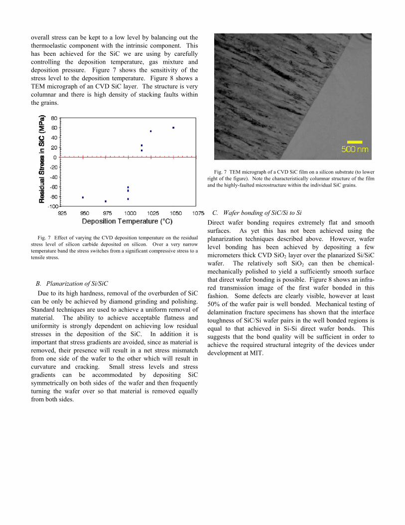
overall stress can be kept to a low level by balancing out the thermoelastic component with the intrinsic component. This has been achieved for the SiC we are using by carefully controlling the deposition temperature, gas mixture and deposition pressure. Figure 7 shows the sensitivity of the stress level to the deposition temperature. Figure 8 shows a TEM micrograph of an CVD SiC layer. The structure is very columnar and there is high density of stacking faults within the grains.
Fig. 7 Effect of varying the CVD deposition temperature on the residual
stress level of silicon carbide deposited on silicon. Over a very narrow temperature band the stress switches from a significant compressive stress to a tensile stress.
B. Planarization of Si/SiC Due to its high hardness, removal of the overburden of SiC
can be only be achieved by diamond grinding and polishing. Standard techniques are used to achieve a uniform removal of material. The ability to achieve acceptable flatness and uniformity is strongly dependent on achieving low residual stresses in the deposition of the SiC. In addition it is important that stress gradients are avoided, since as material is removed, their presence will result in a net stress mismatch from one side of the wafer to the other which will result in curvature and cracking. Small stress levels and stress gradients can be accommodated by depositing SiC symmetrically on both sides of the wafer and then frequently turning the wafer over so that material is removed equally from both sides.
Fig. 7 TEM micrograph of a CVD SiC film on a silicon substrate (to lower
right of the figure). Note the characteristically columnar structure of the film and the highly-faulted microstructure within the individual SiC grains.
C. Wafer bonding of SiC/Si to Si Direct wafer bonding requires extremely flat and smooth surfaces. As yet this has not been achieved using the planarization techniques described above. However, wafer level bonding has been achieved by depositing a few micrometers thick CVD SiO2 layer over the planarized Si/SiC wafer. The relatively soft SiO2 can then be chemical-mechanically polished to yield a sufficiently smooth surface that direct wafer bonding is possible. Figure 8 shows an infra-red transmission image of the first wafer bonded in this fashion. Some defects are clearly visible, however at least 50% of the wafer pair is well bonded. Mechanical testing of delamination fracture specimens has shown that the interface toughness of SiC/Si wafer pairs in the well bonded regions is equal to that achieved in Si-Si direct wafer bonds. This suggests that the bond quality will be sufficient in order to achieve the required structural integrity of the devices under development at MIT.
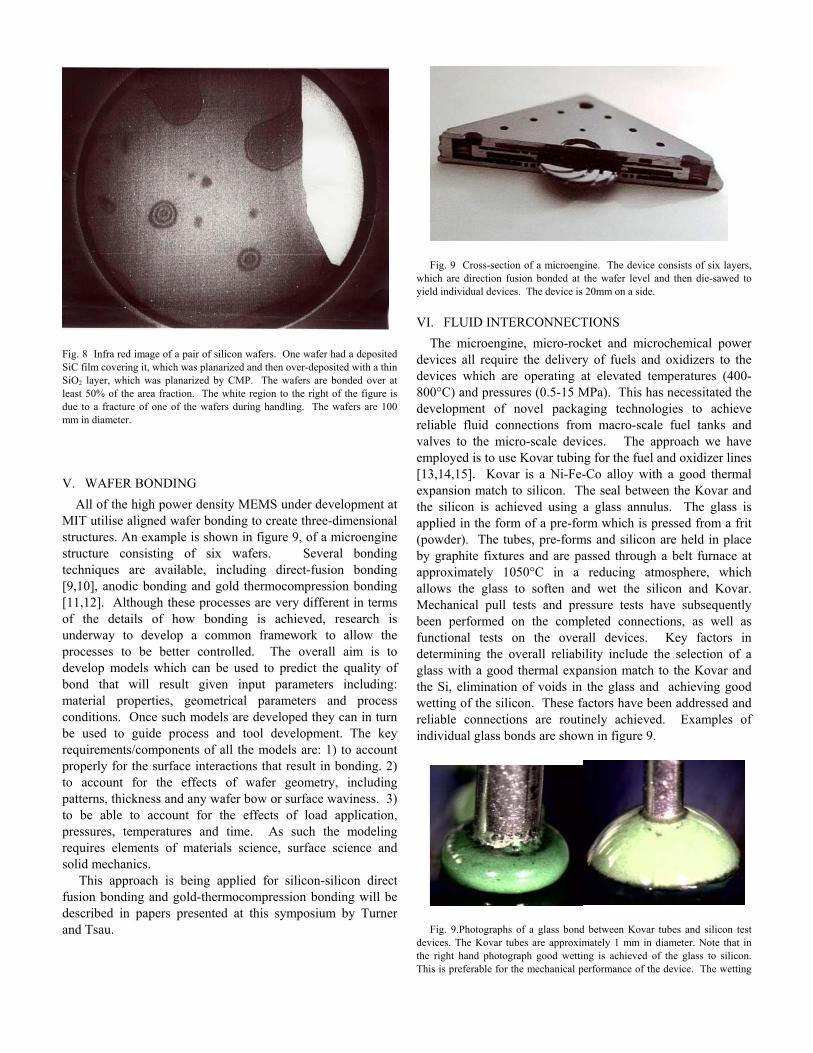
Fig. 8 Infra red image of a pair of silicon wafers. One wafer had a deposited SiC film covering it, which was planarized and then over-deposited with a thin SiO2 layer, which was planarized by CMP. The wafers are bonded over at least 50% of the area fraction. The white region to the right of the figure is due to a fracture of one of the wafers during handling. The wafers are 100 mm in diameter.
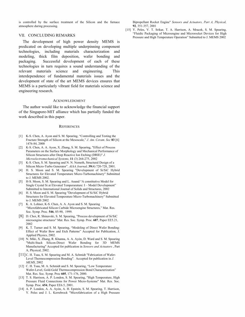
V. WAFER BONDING All of the high power density MEMS under development at
MIT utilise aligned wafer bonding to create three-dimensional structures. An example is shown in figure 9, of a microengine structure consisting of six wafers. Several bonding techniques are available, including direct-fusion bonding [9,10], anodic bonding and gold thermocompression bonding [11,12]. Although these processes are very different in terms of the details of how bonding is achieved, research is underway to develop a common framework to allow the processes to be better controlled. The overall aim is to develop models which can be used to predict the quality of bond that will result given input parameters including: material properties, geometrical parameters and process conditions. Once such models are developed they can in turn be used to guide process and tool development. The key requirements/components of all the models are: 1) to account properly for the surface interactions that result in bonding. 2) to account for the effects of wafer geometry, including patterns, thickness and any wafer bow or surface waviness. 3) to be able to account for the effects of load application, pressures, temperatures and time. As such the modeling requires elements of materials science, surface science and solid mechanics.
This approach is being applied for silicon-silicon direct fusion bonding and gold-thermocompression bonding will be described in papers presented at this symposium by Turner and Tsau.
Fig. 9 Cross-section of a microengine. The device consists of six layers,
which are direction fusion bonded at the wafer level and then die-sawed to yield individual devices. The device is 20mm on a side.
VI. FLUID INTERCONNECTIONS The microengine, micro-rocket and microchemical power
devices all require the delivery of fuels and oxidizers to the devices which are operating at elevated temperatures (400-800°C) and pressures (0.5-15 MPa). This has necessitated the development of novel packaging technologies to achieve reliable fluid connections from macro-scale fuel tanks and valves to the micro-scale devices. The approach we have employed is to use Kovar tubing for the fuel and oxidizer lines [13,14,15]. Kovar is a Ni-Fe-Co alloy with a good thermal expansion match to silicon. The seal between the Kovar and the silicon is achieved using a glass annulus. The glass is applied in the form of a pre-form which is pressed from a frit (powder). The tubes, pre-forms and silicon are held in place by graphite fixtures and are passed through a belt furnace at approximately 1050°C in a reducing atmosphere, which allows the glass to soften and wet the silicon and Kovar. Mechanical pull tests and pressure tests have subsequently been performed on the completed connections, as well as functional tests on the overall devices. Key factors in determining the overall reliability include the selection of a glass with a good thermal expansion match to the Kovar and the Si, elimination of voids in the glass and achieving good wetting of the silicon. These factors have been addressed and reliable connections are routinely achieved. Examples of individual glass bonds are shown in figure 9.
Fig. 9.Photographs of a glass bond between Kovar tubes and silicon test
devices. The Kovar tubes are approximately 1 mm in diameter. Note that in the right hand photograph good wetting is achieved of the glass to silicon. This is preferable for the mechanical performance of the device. The wetting
is controlled by the surface treatment of the Silicon and the furnace atmosphere during processing.
VII. CONCLUDING REMARKS The development of high power density MEMS is
predicated on developing multiple underpinning component technologies, including materials characterization and modeling, thick film deposition, wafer bonding and packaging. Successful development of each of these technologies in turn requires a sound understanding of the relevant materials science and engineering. This interdependence of fundamental materials issues and the development of state of the art MEMS devices ensures that MEMS is a particularly vibrant field for materials science and engineering research.
ACKNOWLEDGMENT The author would like to acknowledge the financial support
of the Singapore-MIT alliance which has partially funded the work described in this paper.
REFERENCES [1] K-S. Chen, A. Ayon and S. M. Spearing, “Controlling and Testing the
Fracture Strength of Silicon at the Mesoscale,” J. Am. Ceram. Soc 83 [6] 1476-84, 2000
[2] K-S. Chen, A. A. Ayon, X. Zhang, S. M. Spearing, "Effect of Process Parameters on the Surface Morphology and Mechanical Performance of Silicon Structures after Deep Reactive Ion Etching (DRIE)" J. Microelectromechanical Systems, 11 (3) 264-275, 2002
[3] K-S. Chen, S. M. Spearing and N. N. Nemeth, Structural Design of a Silicon Micro-Turbo Generator”. AIAA Journal. 39(4) 720-728, 2001.
[4] H. S. Moon and S. M. Spearing "Development of Si/SiC Hybrid Structures for Elevated Temperature Micro-Turbomachinery" Submitted to J. MEMS 2002.
[5] H-S. Moon, S. M. Spearing and L. Anand “A constitutive Model for Single Crystal Si at Elevated Temperarature: I – Model Development” Submitted to International Journal of Solids and Structures, 2002
[6] H. S. Moon and S. M. Spearing "Development of Si/SiC Hybrid Structures for Elevated Temperature Micro-Turbomachinery" Submitted to J. MEMS 2002
[7] K. A. Lohner, K-S. Chen, A. A. Ayon and S. M. Spearing “Microfabricated Silicon Carbide Microengine Structures,” Mat. Res. Soc. Symp. Proc. 546, 85-90, 1999.
[8] D. Choi, R. Shinavski, S. M. Spearing, "Process development of Si/SiC microengine structures" Mat. Res. Soc. Symp. Proc. 687, Paper EE5.21, 2002
[9] K. T. Turner and S. M. Spearing, “Modeling of Direct Wafer Bonding: Effect of Wafer Bow and Etch Patterns” Accepted for Publication, J. Applied Physics, 2002.
[10] N. Miki, X. Zhang, R. Khanna, A. A. Ayón, D. Ward and S. M. Spearing "Multi-Stack Silicon-Direct Wafer Bonding for 3D MEMS Manufacturing" Accepted for publication in Sensors and Actuators , Part A, Physical, 2002.
[11] C. H. Tsau, S. M. Spearing and M. A. Schmidt "Fabrication of Wafer-Level Thermocompression Bonding". Accepted for publication in J. MEMS, 2002
[12] C. H. Tsau, M. A. Schmidt and S. M. Spearing, “Low Temperature Wafer-Level, Gold-Gold Thermocompression Bond Characterization” Mat. Res. Soc. Symp. Proc 605, 171-176, 2000.
[13] T. S. Harrison, A. P. London, S. M. Spearing, "High Temperature, High Pressure Fluid Connections for Power Micro-Systems" Mat. Res. Soc. Symp. Proc. 654, Paper EE6.5, 2001.
[14] A. P. London, A. A. Ayón, A. H. Epstein, S. M. Spearing, T. Harrison, Y. Peles and J. L. Kerrebrock "Microfabrication of a High Pressure
Bipropellant Rocket Engine" Sensors and Actuators, Part A, Physical, 92, 351-357, 2001
[15] Y. Peles, V. T. Srikar, T. A. Harrison, A. Mracek, S. M. Spearing, “Fluidic Packaging of Microengine and Microrocket Devices for High Pressure and High Temperature Operation” Submitted to J. MEMS 2002


![[XLS]ktu.edu · Web viewCircuits and Systems; Processor Architectures; Solid State Physics; Spectroscopy and Microscopy MEMS Materials and Processes Handbook Reza Ghodssi, Pinyen](https://img.pdfslide.us/doc/110x75/5ade9f647f8b9afd1a8b9f51/xlsktuedu-viewcircuits-and-systems-processor-architectures-solid-state-physics.jpg)