Embed Size (px)
Citation preview
MEMS
Class 3
Fabrication Processes for MEMS
Mohammad Kilani
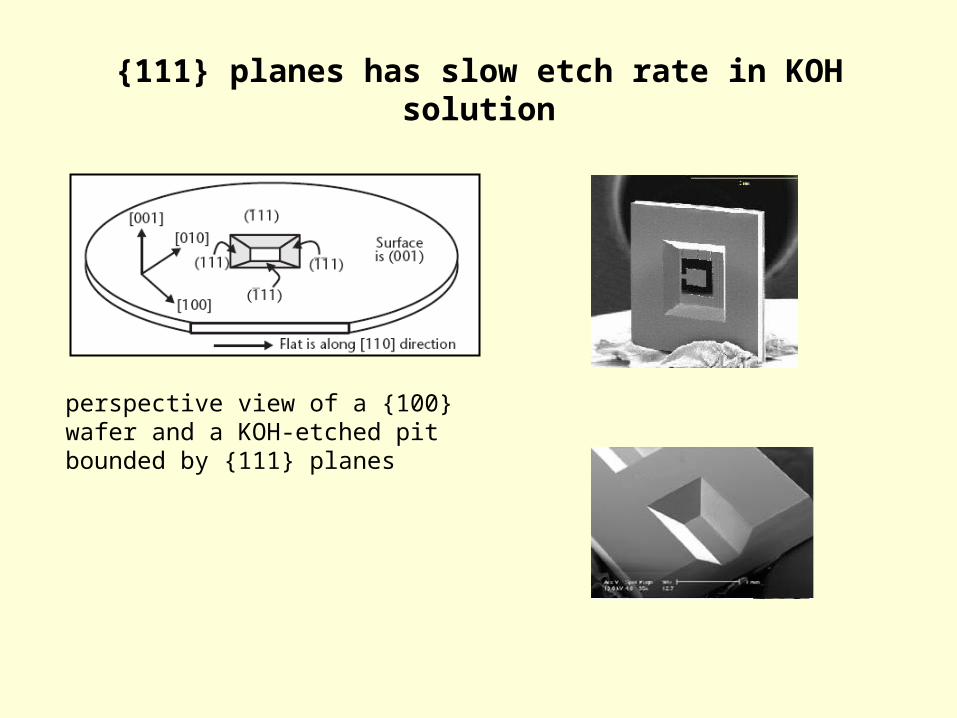
{111} planes has slow etch rate in KOH solution
perspective view of a {100} wafer and a KOH-etched pit bounded by {111} planes
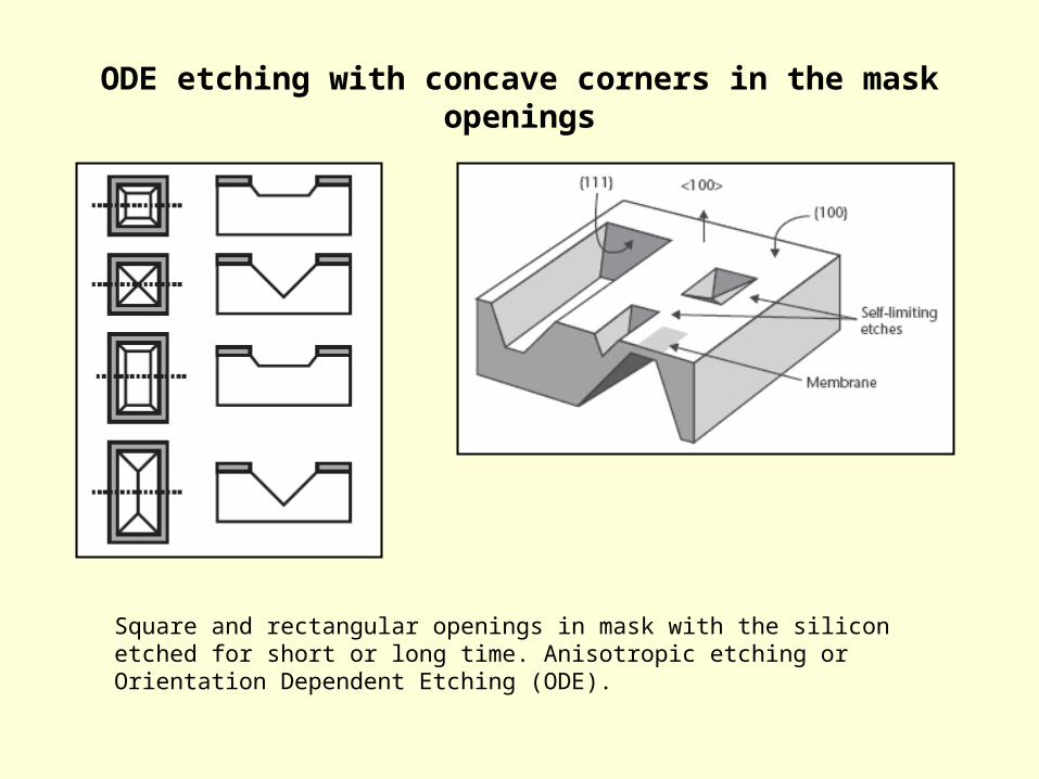
ODE etching with concave corners in the mask openings
Square and rectangular openings in mask with the silicon etched for short or long time. Anisotropic etching or Orientation Dependent Etching (ODE).
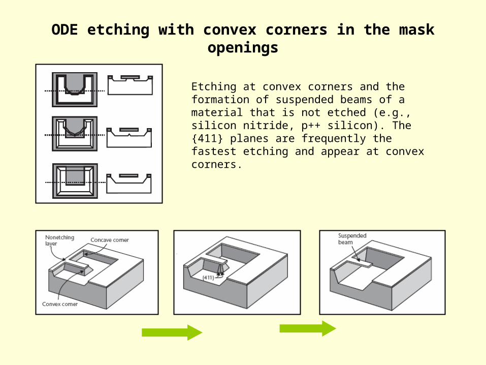
ODE etching with convex corners in the mask openings
Etching at convex corners and the formation of suspended beams of a material that is not etched (e.g., silicon nitride, p++ silicon). The {411} planes are frequently the fastest etching and appear at convex corners.
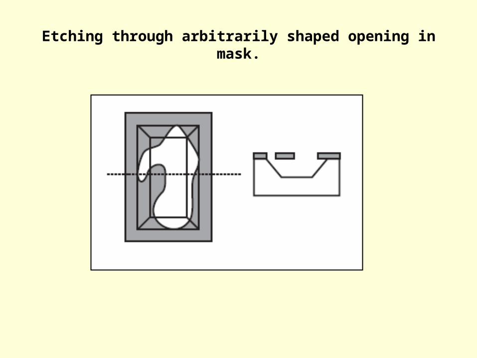
Etching through arbitrarily shaped opening in mask.
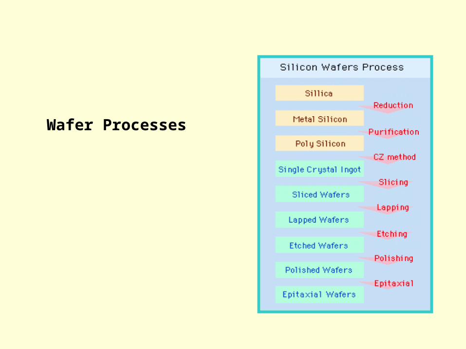
Wafer Processes
Silicon Production by Reduction
• Silicon is commercially prepared by the heating of high-purity silica in an electric arc furnace using carbon electrodes. At temperatures over 1900 °C
• Carbon reduces the silica to silicon according to the chemical equation SiO2 + C → Si + CO2
• Liquid silicon collects in the bottom of the furnace, and is then drained and cooled
• The silicon produced via this process is called metallurgical grade silicon and is at least 99% pure.
• Using this method, silicon carbide, SiC, can form. However, provided the amount of SiO2 is kept high, silicon carbide may be eliminated, as explained by this equation: 2SiC + SiO2 → 3Si + 2CO
• In 2000, metallurgical grade silicon cost about $ 0.56 per pound ($1.23/kg)
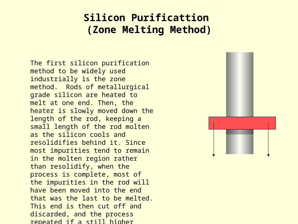
Silicon Purificattion (Zone Melting Method)
The first silicon purification method to be widely used industrially is the zone method. Rods of metallurgical grade silicon are heated to melt at one end. Then, the heater is slowly moved down the length of the rod, keeping a small length of the rod molten as the silicon cools and resolidifies behind it. Since most impurities tend to remain in the molten region rather than resolidify, when the process is complete, most of the impurities in the rod will have been moved into the end that was the last to be melted. This end is then cut off and discarded, and the process repeated if a still higher purity was desired
Silicon Purificattion (Siemens Process)
Today, silicon is purified by converting it to a silicon compound that can be more easily purified than silicon itself, and then converting that silicon compound back into pure silicon. Trichlorosilane is the silicon compound most commonly used as the intermediate. In the Siemens process, high-purity silicon rods are exposed to trichlorosilane at 1150 °C. The trichlorosilane gas decomposes and deposits additional silicon onto the rods, enlarging them according to chemical reactions like
2 HSiCl3 → Si + 2 HCl + SiCl4
Silicon produced from this and similar processes is called polycrystalline silicon. Polycrystalline silicon typically has impurity levels of 1 part per billion or less.
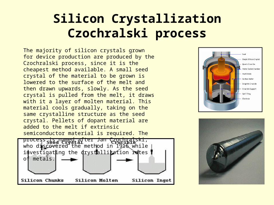
Silicon Crystallization Czochralski process
The majority of silicon crystals grown for device production are produced by the Czochralski process, since it is the cheapest method available. A small seed crystal of the material to be grown is lowered to the surface of the melt and then drawn upwards, slowly. As the seed crystal is pulled from the melt, it draws with it a layer of molten material. This material cools gradually, taking on the same crystalline structure as the seed crystal. Pellets of dopant material are added to the melt if extrinsic semiconductor material is required. The process is named after Jan Czochralski, who discovered the method in 1916 while investigating the crystallization rates of metals.
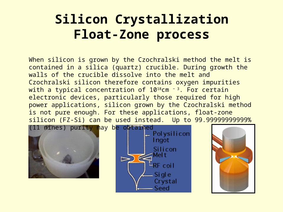
Silicon Crystallization Float-Zone process
When silicon is grown by the Czochralski method the melt is contained in a silica (quartz) crucible. During growth the walls of the crucible dissolve into the melt and Czochralski silicon therefore contains oxygen impurities with a typical concentration of 1018cm − 3. For certain electronic devices, particularly those required for high power applications, silicon grown by the Czochralski method is not pure enough. For these applications, float-zone silicon (FZ-Si) can be used instead. Up to 99.99999999999% (11 nines) purity may be obtained
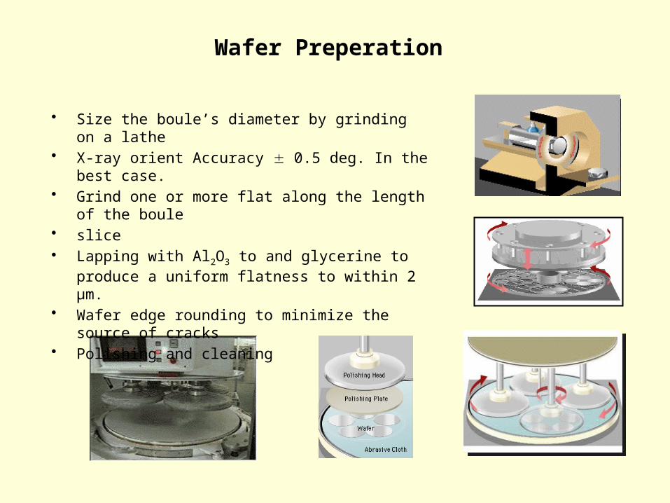
Wafer Preperation
• Size the boule’s diameter by grinding on a lathe• X-ray orient Accuracy 0.5 deg. In the best case.• Grind one or more flat along the length of the boule• slice• Lapping with Al2O3 to and glycerine to produce a
uniform flatness to within 2 µm.• Wafer edge rounding to minimize the source of
cracks• Polishing and cleaning
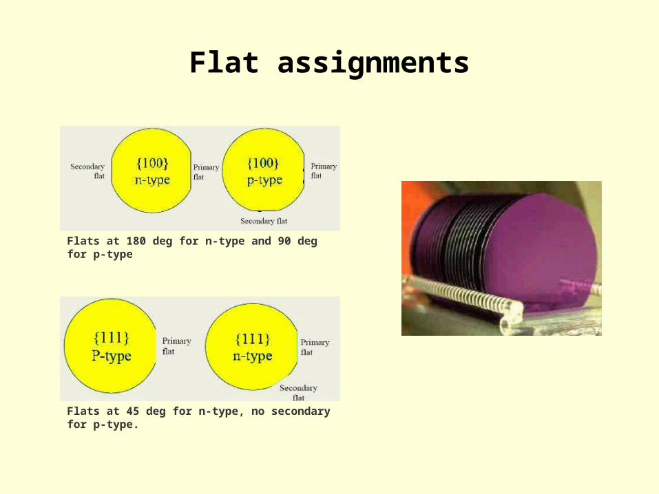
Flat assignments
Flats at 180 deg for n-type and 90 deg for p-type
Flats at 45 deg for n-type, no secondary for p-type.
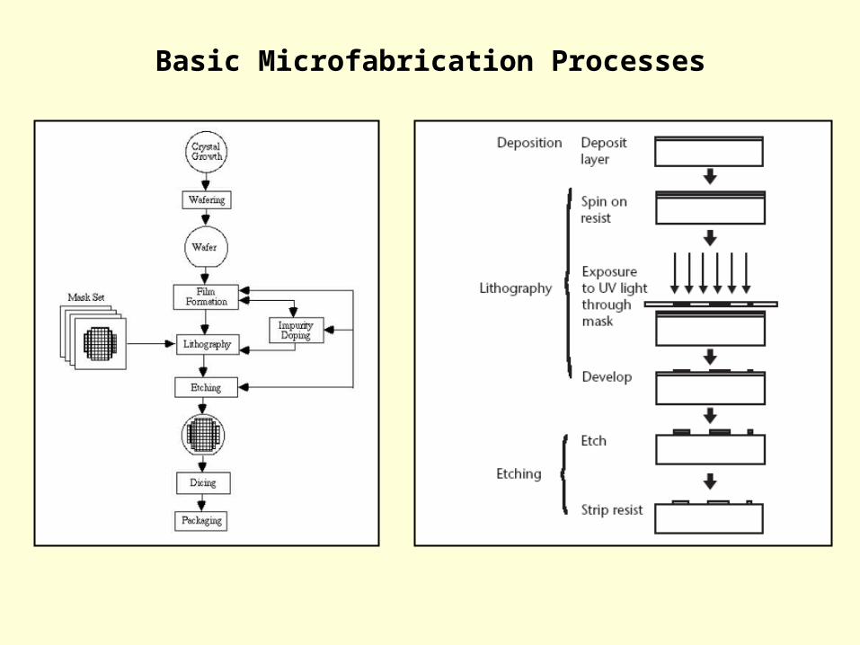
Basic Microfabrication Processes
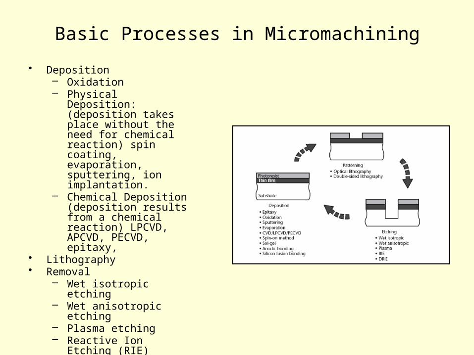
Basic Processes in Micromachining
• Deposition– Oxidation– Physical Deposition:
(deposition takes place without the need for chemical reaction) spin coating, evaporation, sputtering, ion implantation.
– Chemical Deposition (deposition results from a chemical reaction) LPCVD, APCVD, PECVD, epitaxy,
• Lithography• Removal
– Wet isotropic etching– Wet anisotropic etching– Plasma etching– Reactive Ion Etching (RIE)– Deep Reactive Ion Etching
(DRIE)
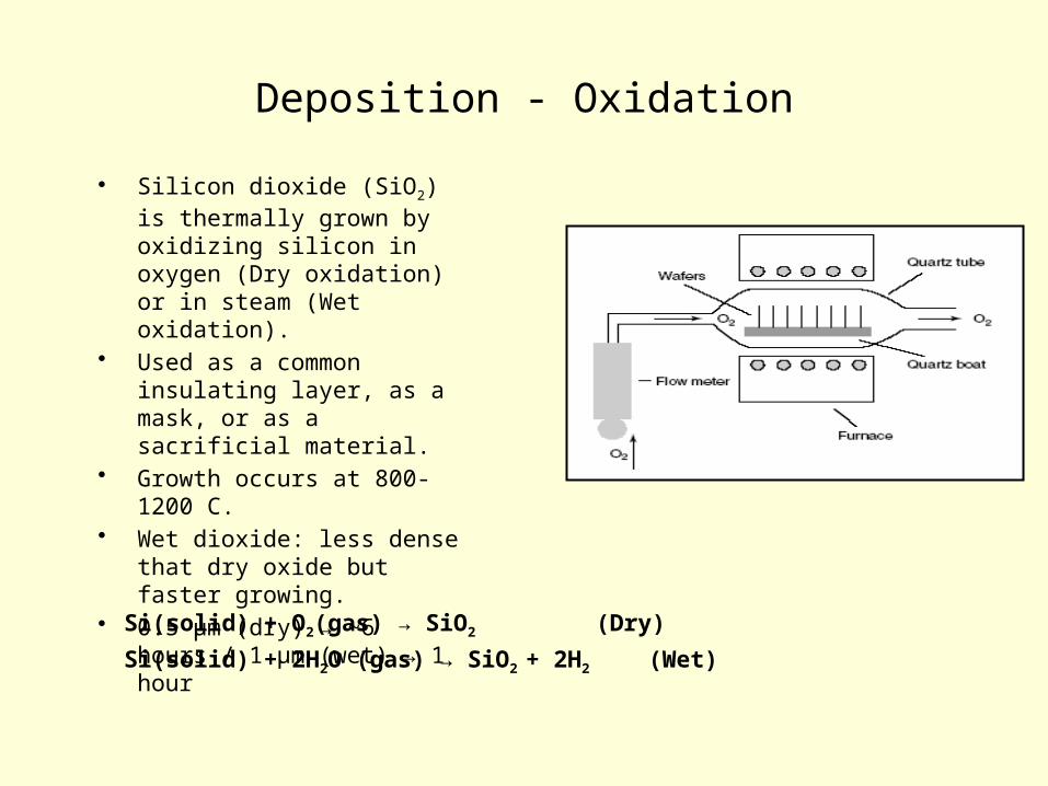
Deposition - Oxidation
• Silicon dioxide (SiO2) is thermally grown by oxidizing silicon in oxygen (Dry oxidation) or in steam (Wet oxidation).
• Used as a common insulating layer, as a mask, or as a sacrificial material.
• Growth occurs at 800-1200 C. • Wet dioxide: less dense that dry
oxide but faster growing.• 0.5 µm (dry) → ~6 hours / 1 µm
(wet) → 1 hour
Si(solid) + O2(gas) → SiO2 (Dry)
Si(solid) + 2H2O (gas) → SiO2 + 2H2 (Wet)
Deposition - Oxidation
Silicon
O2
Silicon
SiO2
Silicon
SiO2
SixNy
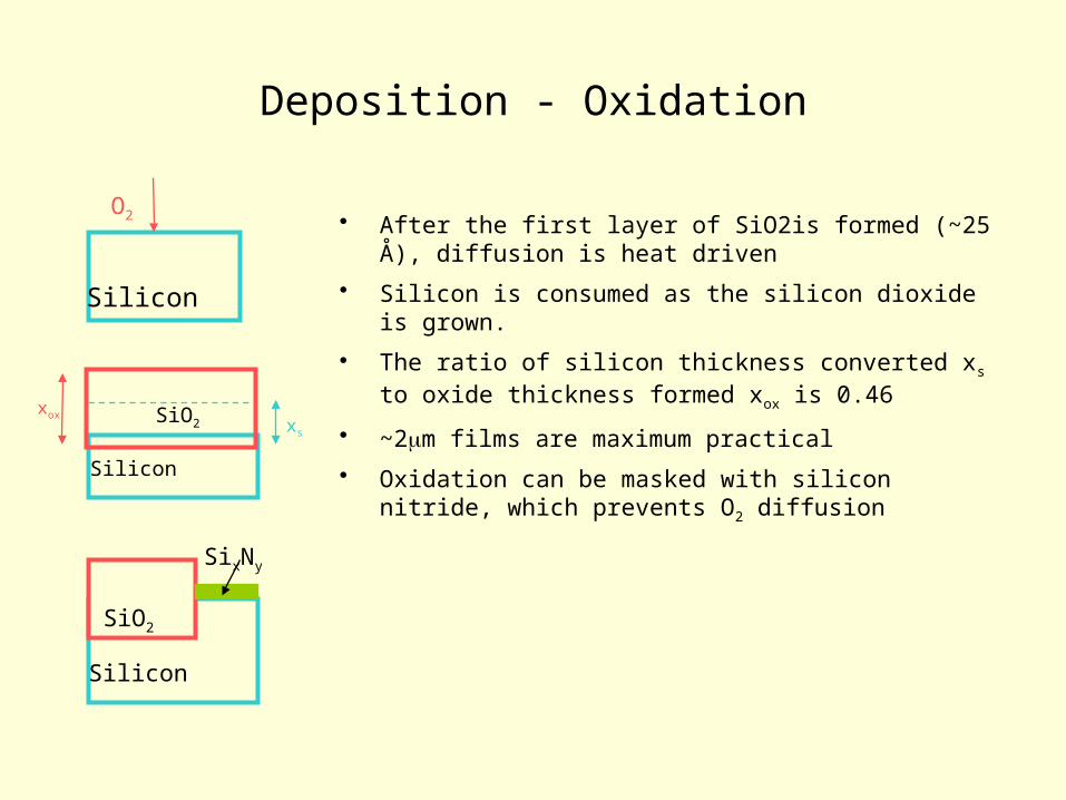
• After the first layer of SiO2is formed (~25 Å), diffusion is heat driven
• Silicon is consumed as the silicon dioxide is grown.
• The ratio of silicon thickness converted xs to oxide thickness formed xox is 0.46
• ~2m films are maximum practical
• Oxidation can be masked with silicon nitride, which prevents O2 diffusion
xoxxs
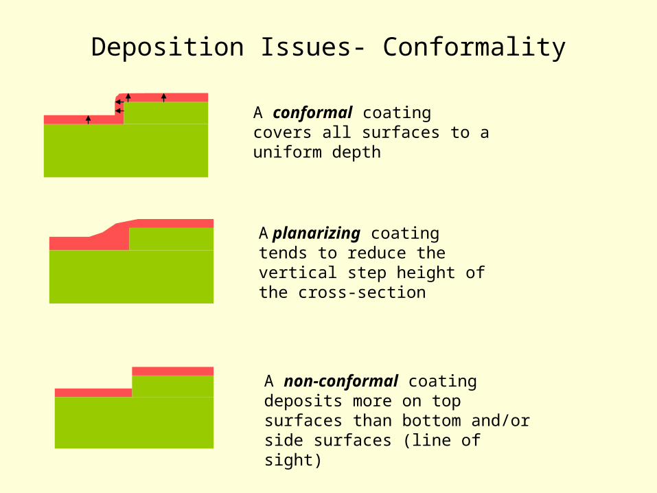
Deposition Issues- Conformality
A conformal coating covers all surfaces to a uniform depth
A planarizing coating tends to reduce the vertical step height of the cross-section
A non-conformal coating deposits more on top surfaces than bottom and/or side surfaces (line of sight)
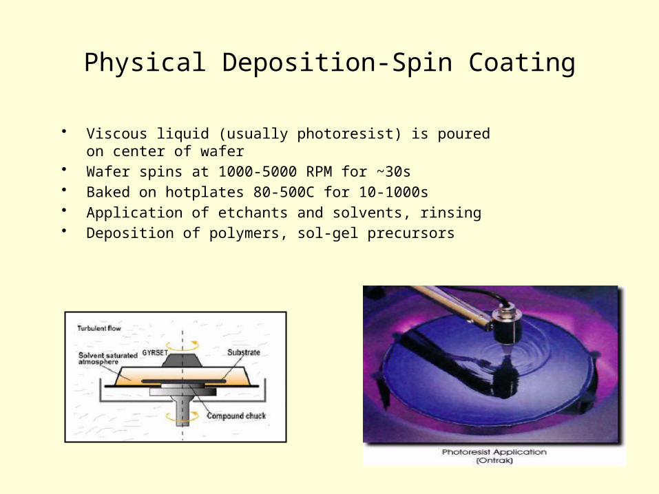
Physical Deposition-Spin Coating
• Viscous liquid (usually photoresist) is poured on center of wafer• Wafer spins at 1000-5000 RPM for ~30s• Baked on hotplates 80-500C for 10-1000s• Application of etchants and solvents, rinsing• Deposition of polymers, sol-gel precursors
Physical Deposition - Evaporation
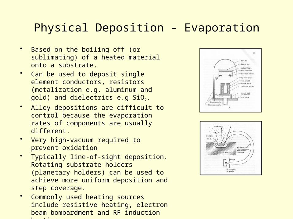
• Based on the boiling off (or sublimating) of a heated material onto a substrate.
• Can be used to deposit single element conductors, resistors (metalization e.g. aluminum and gold) and dielectrics e.g SiO2.
• Alloy depositions are difficult to control because the evaporation rates of components are usually different.
• Very high-vacuum required to prevent oxidation• Typically line-of-sight deposition. Rotating
substrate holders (planetary holders) can be used to achieve more uniform deposition and step coverage.
• Commonly used heating sources include resistive heating, electron beam bombardment and RF induction heating.
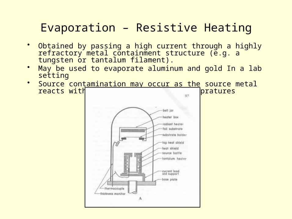
Evaporation – Resistive Heating• Obtained by passing a high current through a highly refractory metal
containment structure (e.g. a tungsten or tantalum filament).• May be used to evaporate aluminum and gold In a lab setting• Source contamination may occur as the source metal reacts with the
crucible at high temepratures
Evaporation – Electron Beam (e-beam)
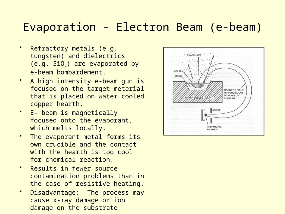
• Refractory metals (e.g. tungsten) and dielectrics (e.g. SiO2) are evaporated by e-beam bombardement.
• A high intensity e-beam gun is focused on the target meterial that is placed on water cooled copper hearth.
• E- beam is magnetically focused onto the evaporant, which melts locally.
• The evaporant metal forms its own crucible and the contact with the hearth is too cool for chemical reaction.
• Results in fewer source contamination problems than in the case of resistive heating.
• Disadvantage: The process may cause x-ray damage or ion damage on the substrate
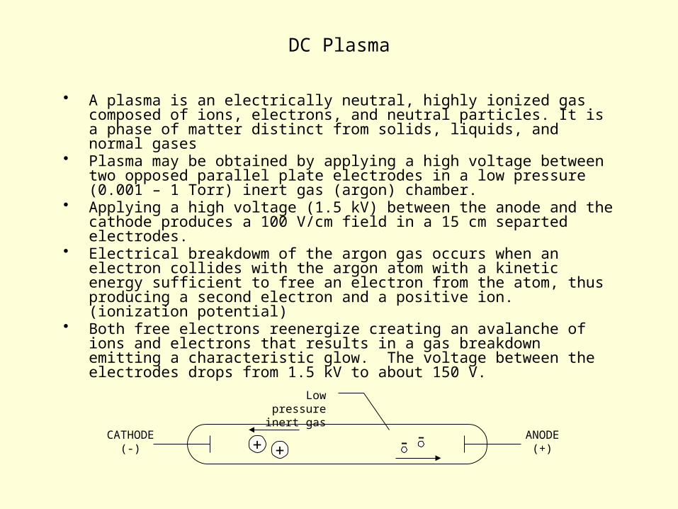
DC Plasma
Low pressure inert gas
CATHODE(-)
ANODE(+)
• A plasma is an electrically neutral, highly ionized gas composed of ions, electrons, and neutral particles. It is a phase of matter distinct from solids, liquids, and normal gases
• Plasma may be obtained by applying a high voltage between two opposed parallel plate electrodes in a low pressure (0.001 – 1 Torr) inert gas (argon) chamber.
• Applying a high voltage (1.5 kV) between the anode and the cathode produces a 100 V/cm field in a 15 cm separted electrodes.
• Electrical breakdowm of the argon gas occurs when an electron collides with the argon atom with a kinetic energy sufficient to free an electron from the atom, thus producing a second electron and a positive ion. (ionization potential)
• Both free electrons reenergize creating an avalanche of ions and electrons that results in a gas breakdown emitting a characteristic glow. The voltage between the electrodes drops from 1.5 kV to about 150 V.
+ +--
DC Plasma
Low pressure inert gas
CATHODE(-)
ANODE(+)
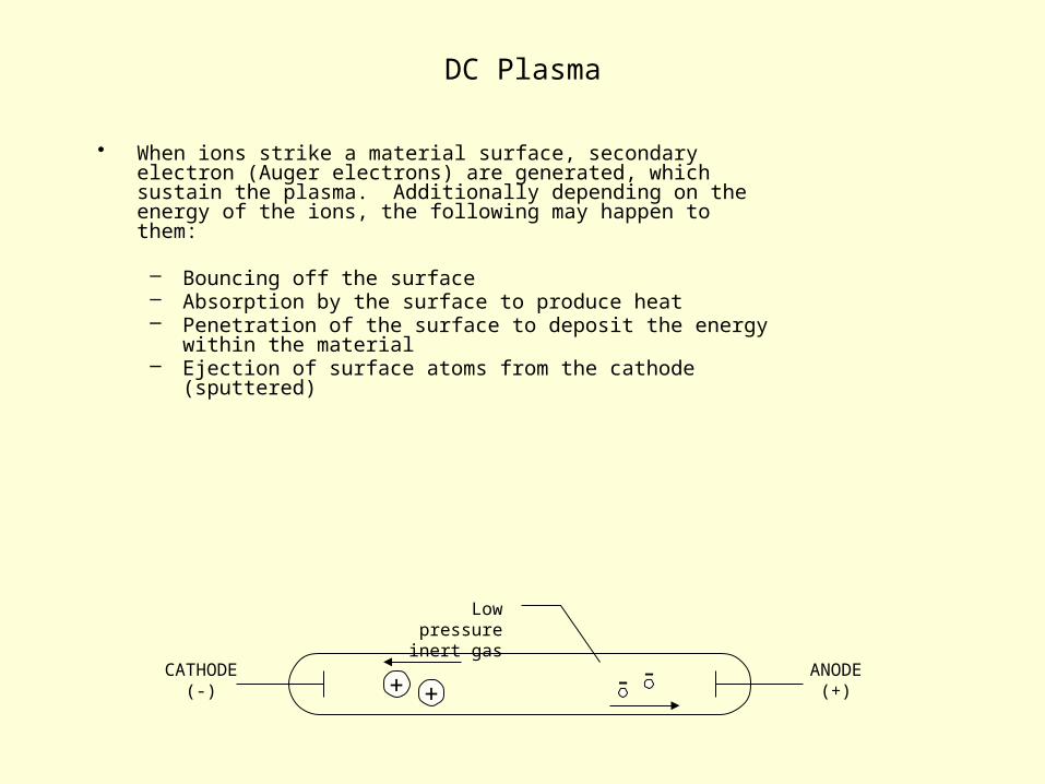
• When ions strike a material surface, secondary electron (Auger electrons) are generated, which sustain the plasma. Additionally depending on the energy of the ions, the following may happen to them:
– Bouncing off the surface– Absorption by the surface to produce heat– Penetration of the surface to deposit the energy within the
material– Ejection of surface atoms from the cathode (sputtered)
+ +--
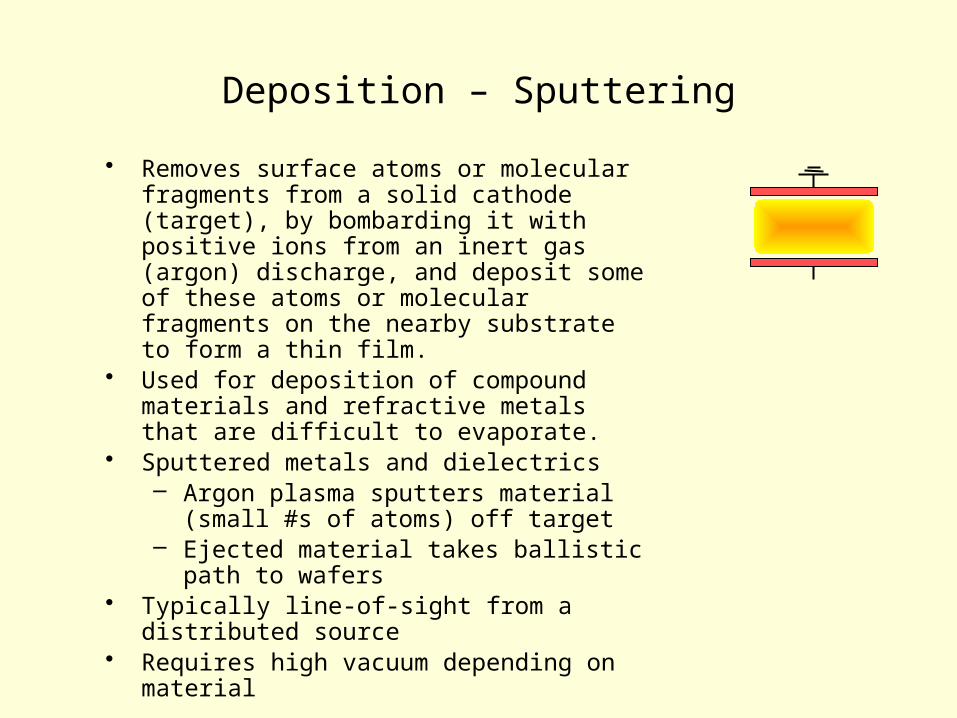
Deposition – Sputtering
• Removes surface atoms or molecular fragments from a solid cathode (target), by bombarding it with positive ions from an inert gas (argon) discharge, and deposit some of these atoms or molecular fragments on the nearby substrate to form a thin film.
• Used for deposition of compound materials and refractive metals that are difficult to evaporate.
• Sputtered metals and dielectrics– Argon plasma sputters material (small #s of
atoms) off target– Ejected material takes ballistic path to
wafers• Typically line-of-sight from a distributed source• Requires high vacuum depending on material
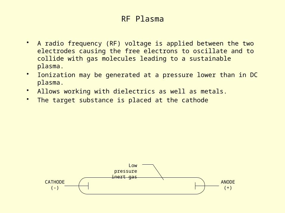
RF Plasma
Low pressure inert gas
CATHODE(-)
ANODE(+)
• A radio frequency (RF) voltage is applied between the two electrodes causing the free electrons to oscillate and to collide with gas molecules leading to a sustainable plasma.
• Ionization may be generated at a pressure lower than in DC plasma.• Allows working with dielectrics as well as metals.• The target substance is placed at the cathode
Deposition Issues - Compatibility
• Thermal compatibility– Thermal oxidation and LPCVD films are mutually compatible– Thermal oxidation and LPCVD are not compatible with polymers
(melting/burning) and most metals (eutectic formation, diffusion, furnace contamination)
• Topographic compatibility– Can not spin-cast over large step heights– Distributed-source deposition over deep trenches leaves keyholes
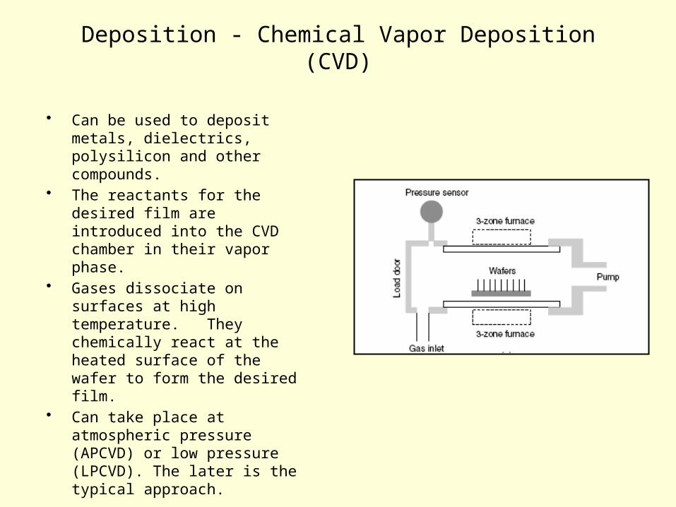
Deposition - Chemical Vapor Deposition (CVD)
• Can be used to deposit metals, dielectrics, polysilicon and other compounds.
• The reactants for the desired film are introduced into the CVD chamber in their vapor phase.
• Gases dissociate on surfaces at high temperature. They chemically react at the heated surface of the wafer to form the desired film.
• Can take place at atmospheric pressure (APCVD) or low pressure (LPCVD). The later is the typical approach.
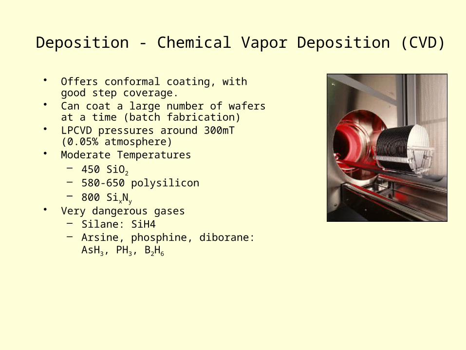
• Offers conformal coating, with good step coverage.
• Can coat a large number of wafers at a time (batch fabrication)
• LPCVD pressures around 300mT (0.05% atmosphere)
• Moderate Temperatures– 450 SiO2
– 580-650 polysilicon– 800 SixNy
• Very dangerous gases– Silane: SiH4– Arsine, phosphine, diborane: AsH3, PH3,
B2H6
Deposition - Chemical Vapor Deposition (CVD)
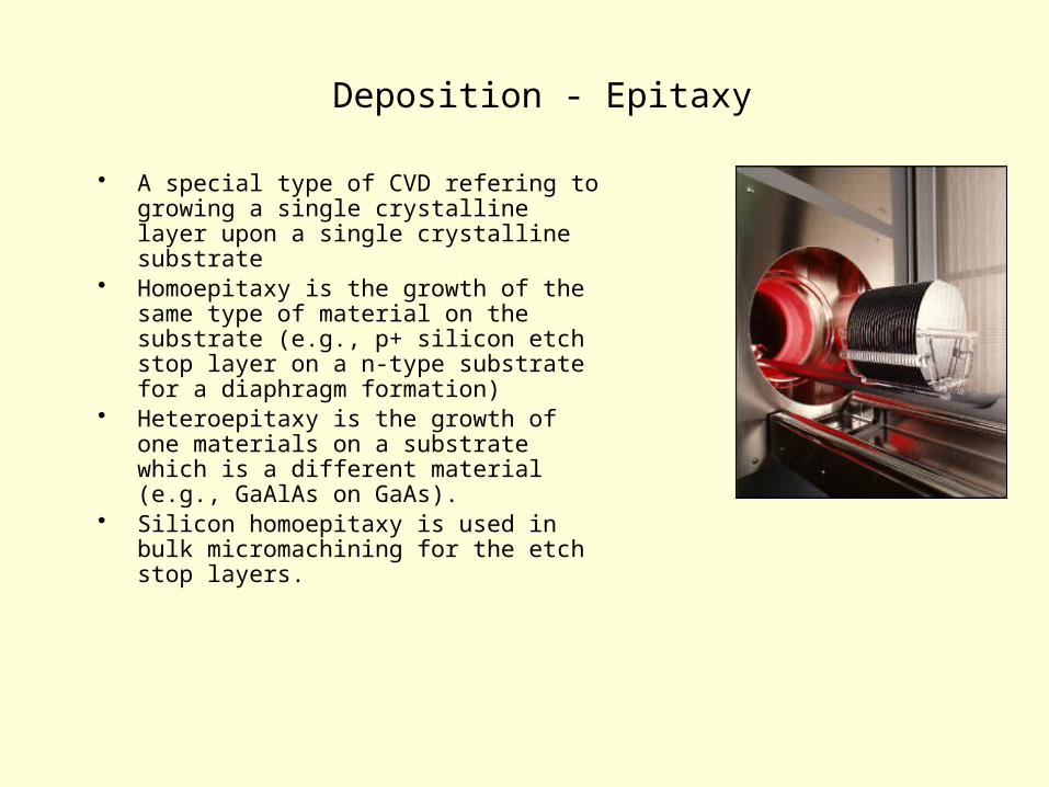
• A special type of CVD refering to growing a single crystalline layer upon a single crystalline substrate
• Homoepitaxy is the growth of the same type of material on the substrate (e.g., p+ silicon etch stop layer on a n-type substrate for a diaphragm formation)
• Heteroepitaxy is the growth of one materials on a substrate which is a different material (e.g., GaAlAs on GaAs).
• Silicon homoepitaxy is used in bulk micromachining for the etch stop layers.
Deposition - Epitaxy
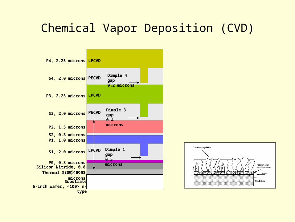
Chemical Vapor Deposition (CVD)
Thermal SiO2, 0.63 micronsSilicon Nitride, 0.8 microns
P0, 0.3 microns
S1, 2.0 microns
P1, 1.0 micronsS2, 0.3 microns
Substrate6-inch wafer, <100> n-type
P2, 1.5 microns
S3, 2.0 microns
P3, 2.25 microns
S4, 2.0 microns
P4, 2.25 microns
LPCVD
LPCVD
PECVD
PECVD
Dimple 1 gap0.5 microns
Dimple 3 gap0.4 microns
Dimple 4 gap0.2 microns
LPCVD
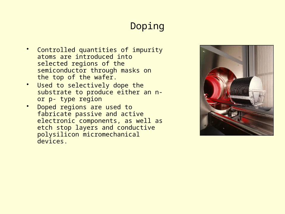
• Controlled quantities of impurity atoms are introduced into selected regions of the semiconductor through masks on the top of the wafer.
• Used to selectively dope the substrate to produce either an n- or p- type region
• Doped regions are used to fabricate passive and active electronic components, as well as etch stop layers and conductive polysilicon micromechanical devices.
Doping
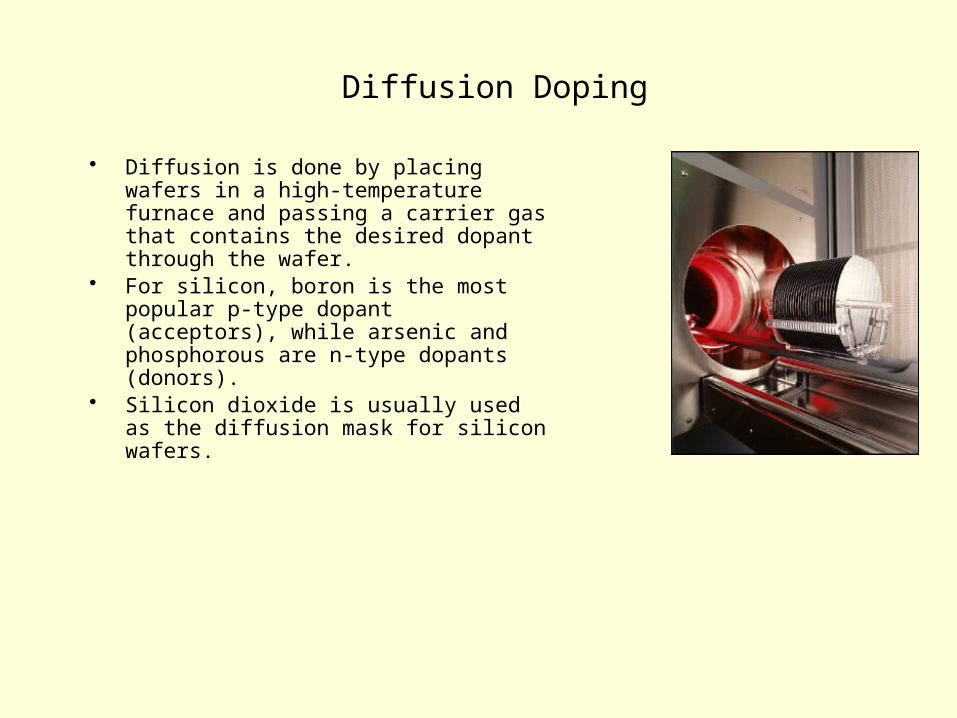
• Diffusion is done by placing wafers in a high-temperature furnace and passing a carrier gas that contains the desired dopant through the wafer.
• For silicon, boron is the most popular p-type dopant (acceptors), while arsenic and phosphorous are n-type dopants (donors).
• Silicon dioxide is usually used as the diffusion mask for silicon wafers.
Diffusion Doping
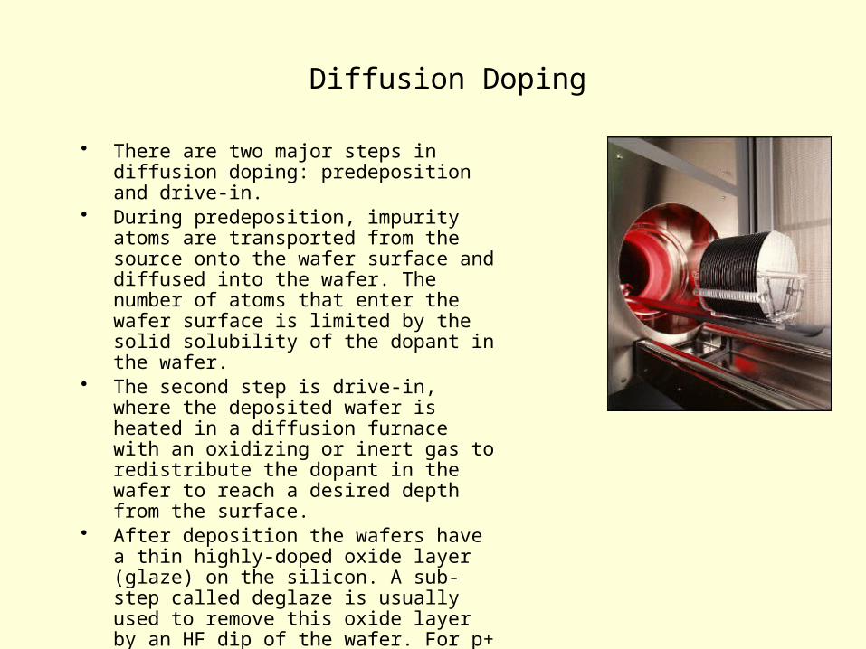
• There are two major steps in diffusion doping: predeposition and drive-in.
• During predeposition, impurity atoms are transported from the source onto the wafer surface and diffused into the wafer. The number of atoms that enter the wafer surface is limited by the solid solubility of the dopant in the wafer.
• The second step is drive-in, where the deposited wafer is heated in a diffusion furnace with an oxidizing or inert gas to redistribute the dopant in the wafer to reach a desired depth from the surface.
• After deposition the wafers have a thin highly-doped oxide layer (glaze) on the silicon. A sub-step called deglaze is usually used to remove this oxide layer by an HF dip of the wafer. For p+ (a very heavily doped) predeposited wafers, a low temperature oxidation process may be used to facilitate the removal of the "glaze" layer.
Diffusion Doping
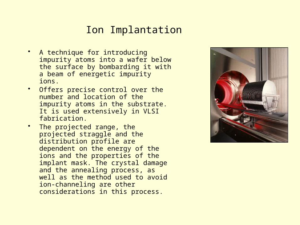
• A technique for introducing impurity atoms into a wafer below the surface by bombarding it with a beam of energetic impurity ions.
• Offers precise control over the number and location of the impurity atoms in the substrate. It is used extensively in VLSI fabrication.
• The projected range, the projected straggle and the distribution profile are dependent on the energy of the ions and the properties of the implant mask. The crystal damage and the annealing process, as well as the method used to avoid ion-channeling are other considerations in this process.
Ion Implantation
Photolithography
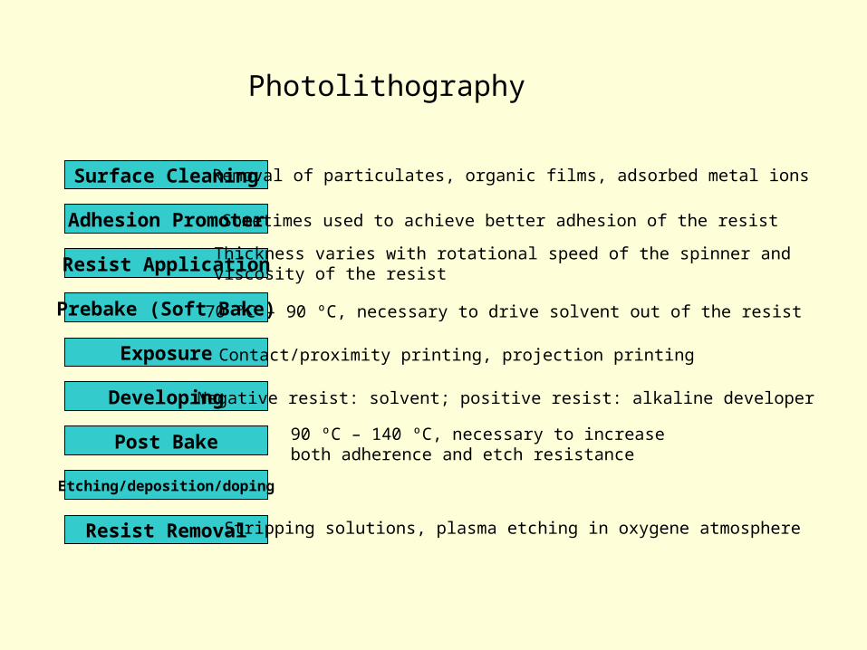
Surface Cleaning
Adhesion Promoter
Resist Application
Prebake (Soft Bake)
Exposure
Developing
Post Bake
Etching/deposition/doping
Removal of particulates, organic films, adsorbed metal ions
Sometimes used to achieve better adhesion of the resist
Thickness varies with rotational speed of the spinner andviscosity of the resist
70 °C – 90 ºC, necessary to drive solvent out of the resist
Contact/proximity printing, projection printing
Negative resist: solvent; positive resist: alkaline developer
90 ºC – 140 ºC, necessary to increase both adherence and etch resistance
Resist Removal Stripping solutions, plasma etching in oxygene atmosphere
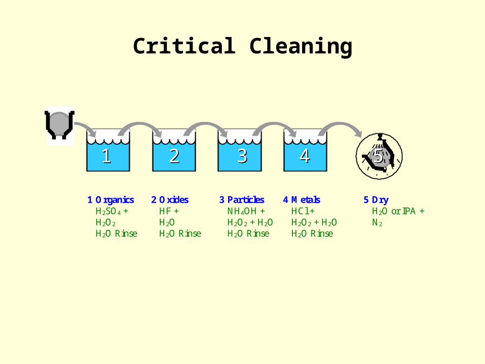
Critical Cleaning
11 22 33 44 55
1 Organics 2 Oxides 3 Particles 4 Metals 5 DryH2SO4 + HF + NH4OH + HCl + H2O or IPA +H2O2 H2O H2O2 + H2O H2O2 + H2O N2
H2O Rinse H2O Rinse H2O Rinse H2O Rinse