Embed Size (px)
Citation preview

Memristor-based memory: The sneak paths problem andsolutions
KAUSTRepository
Item type Article
Authors Zidan, Mohammed A.; Fahmy, Hossam A.H.; Hussain,Muhammad Mustafa; Salama, Khaled N.
Citation Zidan MA, Fahmy HAH, Hussain MM, Salama KN (2013)Memristor-based memory: The sneak paths problem andsolutions. Microelectronics Journal 44: 176-183.doi:10.1016/j.mejo.2012.10.001.
Eprint version Post-print
DOI 10.1016/j.mejo.2012.10.001
Publisher Elsevier BV
Journal Microelectronics Journal
Rights Archived with thanks to Microelectronics Journal
Downloaded 16-May-2018 23:43:30
Link to item http://hdl.handle.net/10754/250453
Memristor-based Memory: The Sneak Paths Problem and Solutions
Mohammed Affan Zidana, Hossam Aly Hassan Fahmyb, Muhammad Mustafa Hussaina, Khaled Nabil Salamaa
aElectrical Engineering, King Abdullah University of Science and Technology (KAUST), Thuwal 23955-6900, Saudi ArabiabElectronics and Communication Department, Faculty of Engineering, Cairo University, Cairo, Egypt
Abstract
In this paper, we investigate the read operation of memristor-based memories. We analyze the sneak paths problem and provide anoise margin metric to compare the various solutions proposed in the literature. We also analyze the power consumption associatedwith these solutions. Moreover, we study the effect of the aspect ratio of the memory array on the sneak paths. Finally, we introducea new technique for solving the sneak paths problem by gating the memory cell using a three-terminal memistor device.
Keywords: Nanotechnology, Memory, Memory Array, Memristor, Sneak Paths
1. Introduction
Memristors (memory resistors) offer a promising alternativeto conventional memory devices. According to the Interna-tional Technology Road-map for Semiconductors (ITRS), cur-rent memory technologies (DRAM, SRAM, and NAND Flash)will soon be facing design challenges related to their contin-ued scaling-down [1]. Memristors are considered to be a verygood candidate for future memory devices when compared toother emerging technologies such as Magnetoresistive RAM(MRAM) and Phase Change RAM (PCM/PCRAM) [2]. Themain advantage these emerging technologies share is the prop-erty of retaining data after bias removal. Moreover, memristor-based memories have many unique advantages including veryhigh density compared to other memory technologies and harddisk drives.
The memristor is a nonlinear resistor which changes its staterelative to the net charge (or net electric flux) passing throughits two terminals. It saves its state after an electrical bias isremoved. The memristor (M), which was described by Chuain 1971 [3], is generally thought of as the fourth of the two-terminal basic passive elements, alongside the resistor (R), ca-pacitor (C), and inductor (L). The first reported passive imple-mentation of the memristor was the TiO2-based device intro-duced by HP in 2008 [4]. Recently, devices based on differentmaterials have been introduced [5–9]. In addition, several mod-els for memristors has been introduced [10–16]. Since the firstreported use of the memristor, it received a significant of at-tention in the research community. In addition to be used asa memory element [2, 17–26], the memristor has found manyapplications in oscillators [27–30], logic and arithmetic cir-cuits [31, 32], programmable analog circuits [33, 34], and inmodeling and emulation of natural phenomena [35, 36].
Email addresses: [email protected] (Mohammed AffanZidan), [email protected] (Hossam Aly Hassan Fahmy),[email protected] (Muhammad MustafaHussain), [email protected] (Khaled Nabil Salama)
One of the main challenges facing the memristor at the circuitand architecture level is the sneak paths problem. In this paperwe introduce a new way to analyze the sneak paths using nor-malized noise margins. Our analysis is based on simulations fordifferent memory array sizes, data sets, and architectures usingthe models presented in [17]. Moreover, we study the effect ofthe aspect ratio of the memory array on the sneak paths. Finally,a new method is introduce for solving the sneak paths based ona new gating technique by using three-terminal memistor deviceas a gate for the memristor memory cell.
The following section discusses the main concept of thememristor-based memory. The Section 3 describes the sneakpaths analysis, and Section 4 summarized the main solutionsfor the sneak paths that have been described in the literature.Then, the new proposed solution is given in Section 5.
2. Memristor-Based Memory
Memristor-based memories are fabricated as a high-densitycrossbar architecture. Memristor devices are located at eachintersection between two bars, as shown in Fig. 1. Typicalmemristor-based memories do not use transistors for cell gat-ing. The advantage of these devices is that they have a retain-able memory and a very high density compared to other storage
Figure 1: A simple memristor-based memory array showinghow a memristor device is located at the intersection betweentwo bars of the array.
Preprint submitted to Microelectronics Journal October 29, 2012
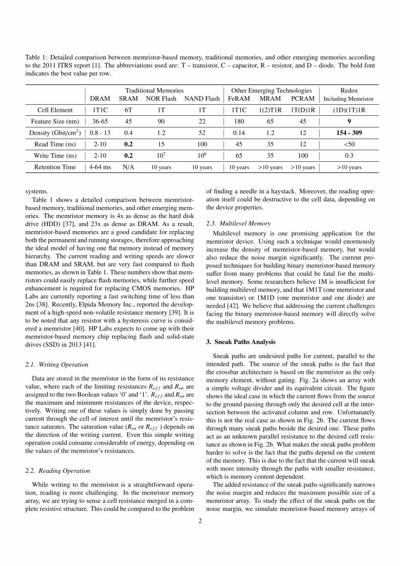
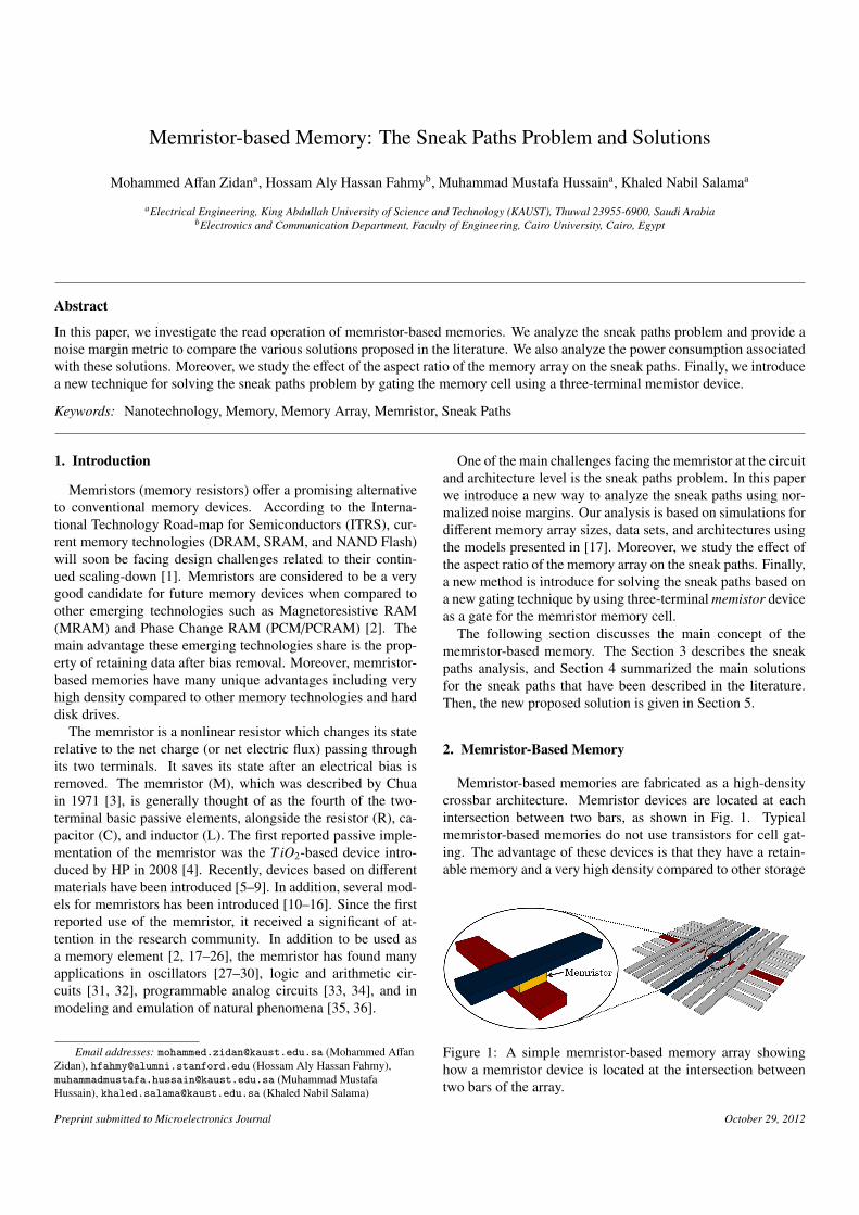
Table 1: Detailed comparison between memristor-based memory, traditional memories, and other emerging memories accordingto the 2011 ITRS report [1]. The abbreviations used are: T – transistor, C – capacitor, R – resistor, and D – diode. The bold fontindicates the best value per row.
Traditional Memories Other Emerging Technologies RedoxDRAM SRAM NOR Flash NAND Flash FeRAM MRAM PCRAM Including Memristor
Cell Element 1T1C 6T 1T 1T 1T1C 1(2)T1R 1T(D)1R (1D)(1T)1R
Feature Size (nm) 36-65 45 90 22 180 65 45 9
Density (Gbit/cm2) 0.8 - 13 0.4 1.2 52 0.14 1.2 12 154 - 309
Read Time (ns) 2-10 0.2 15 100 45 35 12 <50
Write Time (ns) 2-10 0.2 107 106 65 35 100 0.3
Retention Time 4-64 ms N/A 10 years 10 years 10 years >10 years >10 years >10 years
systems.Table 1 shows a detailed comparison between memristor-
based memory, traditional memories, and other emerging mem-ories. The memristor memory is 4x as dense as the hard diskdrive (HDD) [37], and 23x as dense as DRAM. As a result,memristor-based memories are a good candidate for replacingboth the permanent and running storages, therefore approachingthe ideal model of having one flat memory instead of memoryhierarchy. The current reading and writing speeds are slowerthan DRAM and SRAM, but are very fast compared to flashmemories, as shown in Table 1. These numbers show that mem-ristors could easily replace flash memories, while further speedenhancement is required for replacing CMOS memories. HPLabs are currently reporting a fast switching time of less than2ns [38]. Recently, Elpida Memory Inc., reported the develop-ment of a high-speed non-volatile resistance memory [39]. It isto be noted that any resistor with a hysteresis curve is consid-ered a memristor [40]. HP Labs expects to come up with theirmemristor-based memory chip replacing flash and solid-statedrives (SSD) in 2013 [41].
2.1. Writing Operation
Data are stored in the memristor in the form of its resistancevalue, where each of the limiting resistances Ro f f and Ron areassigned to the two Boolean values ‘0’ and ‘1’. Ro f f and Ron arethe maximum and minimum resistances of the device, respec-tively. Writing one of these values is simply done by passingcurrent through the cell of interest until the memristor’s resis-tance saturates. The saturation value (Ron or Ro f f ) depends onthe direction of the writing current. Even this simple writingoperation could consume considerable of energy, depending onthe values of the memristor’s resistances.
2.2. Reading Operation
While writing to the memristor is a straightforward opera-tion, reading is more challenging. In the memristor memoryarray, we are trying to sense a cell resistance merged in a com-plete resistive structure. This could be compared to the problem
of finding a needle in a haystack. Moreover, the reading oper-ation itself could be destructive to the cell data, depending onthe device properties.
2.3. Multilevel Memory
Multilevel memory is one promising application for thememristor device. Using such a technique would enormouslyincrease the density of memristor-based memory, but wouldalso reduce the noise margin significantly. The current pro-posed techniques for building binary memristor-based memorysuffer from many problems that could be fatal for the multi-level memory. Some researchers believe 1M is insufficient forbuilding multilevel memory, and that 1M1T (one memristor andone transistor) or 1M1D (one memristor and one diode) areneeded [42]. We believe that addressing the current challengesfacing the binary memristor-based memory will directly solvethe multilevel memory problems.
3. Sneak Paths Analysis
Sneak paths are undesired paths for current, parallel to theintended path. The source of the sneak paths is the fact thatthe crossbar architecture is based on the memristor as the onlymemory element, without gating. Fig. 2a shows an array witha simple voltage divider and its equivalent circuit. The figureshows the ideal case in which the current flows from the sourceto the ground passing through only the desired cell at the inter-section between the activated column and row. Unfortunatelythis is not the real case as shown in Fig. 2b. The current flowsthrough many sneak paths beside the desired one. These pathsact as an unknown parallel resistance to the desired cell resis-tance as shown in Fig. 2b. What makes the sneak paths problemharder to solve is the fact that the paths depend on the contentof the memory. This is due to the fact that the current will sneakwith more intensity through the paths with smaller resistance,which is memory content dependent.
The added resistance of the sneak paths significantly narrowsthe noise margin and reduces the maximum possible size of amemristor array. To study the effect of the sneak paths on thenoise margin, we simulate memristor-based memory arrays of
2
VRVR
RL
Vo
RL
RM
Vo
(a)
VRVR
RL
Vo
RL
RM
Vo
RSP
Memristor
Desired Path
Sneak Path
(b)
Figure 2: The reading current path through a memristor memory array and the equivalent circuit for (a) the ideal case where thecurrent flows only through the target cell and (b) an example of a real case where current sneaks through different undesired paths.The green lines show the desired path and the red ones show the effective sneak paths.
different sizes and with different data sets. The sets are selectedto reflect both the worst and best cases for the memory content.The worst case for the sneak paths is a memory full of “ones”since the effect of the sneak paths becomes more dominant astheir resistance decreases. On the other hand the “all zeros”case is the best case condition since all the sneak paths are madeof Ro f f resistances in series. In addition to the previous cases,checkered cases typical of real data and interleaved rows (orcolumns) are also used. These cases are considered as normaltest cases since ones and zeros are present in equal numbers andare uniformly distributed. The simulation result is independentof the location of the cell in the array if we neglect the rows’and columns’ pad resistances. We can interpret the array as acomplete sphere, since connecting the terminals of each row orcolumn will not introduce any change to the equivalent circuitas shown in Fig. 3. Hence all the cell locations are equivalentfrom the sneak paths point of view. All the simulations weremade on Cadence Virtuoso 6 with a reading voltage (VR) of’1V’ and a load resistance (RL) of 19.76MΩ.
As our basic building block, we used the model in [17] forthe memristor as a memory cell, such that:
IM = kx sinh(aV) (1)
≡
Figure 3: Two equivalent arrays from the sneak paths point ofview.
where a and kx are constants. The reported feasible valuesin [17] for the constants are a = 3−1 and kon = 10−8A andko f f = 10−11A for the ON and OFF states of the device respec-tively.
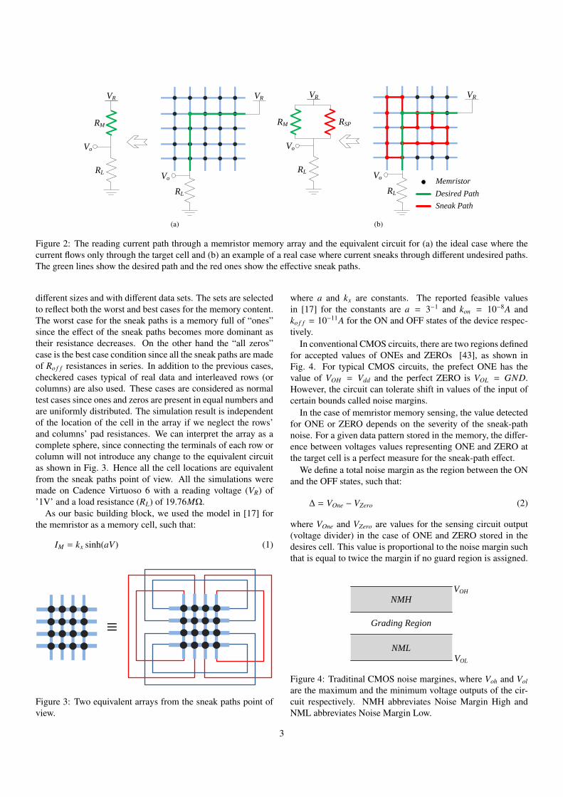
In conventional CMOS circuits, there are two regions definedfor accepted values of ONEs and ZEROs [43], as shown inFig. 4. For typical CMOS circuits, the prefect ONE has thevalue of VOH = Vdd and the perfect ZERO is VOL = GND.However, the circuit can tolerate shift in values of the input ofcertain bounds called noise margins.
In the case of memristor memory sensing, the value detectedfor ONE or ZERO depends on the severity of the sneak-pathnoise. For a given data pattern stored in the memory, the differ-ence between voltages values representing ONE and ZERO atthe target cell is a perfect measure for the sneak-path effect.
We define a total noise margin as the region between the ONand the OFF states, such that:
∆ = VOne − VZero (2)
where VOne and VZero are values for the sensing circuit output(voltage divider) in the case of ONE and ZERO stored in thedesires cell. This value is proportional to the noise margin suchthat is equal to twice the margin if no guard region is assigned.
Grading Region
NMH
NML
VOH
VOL
Figure 4: Traditinal CMOS noise margines, where Voh and Vol
are the maximum and the minimum voltage outputs of the cir-cuit respectively. NMH abbreviates Noise Margin High andNML abbreviates Noise Margin Low.
3
To study the effect of the array size on the sneak-paths we de-fined a normalized value, where the ∆ is compared to its bestcase, as:
∆′ =∆Array
∆Device(3)
where ∆Device is the case of one device used (the best case) while∆Array is for the array case. ∆Array is highly dependent on thedata stored in the memory as shown later.
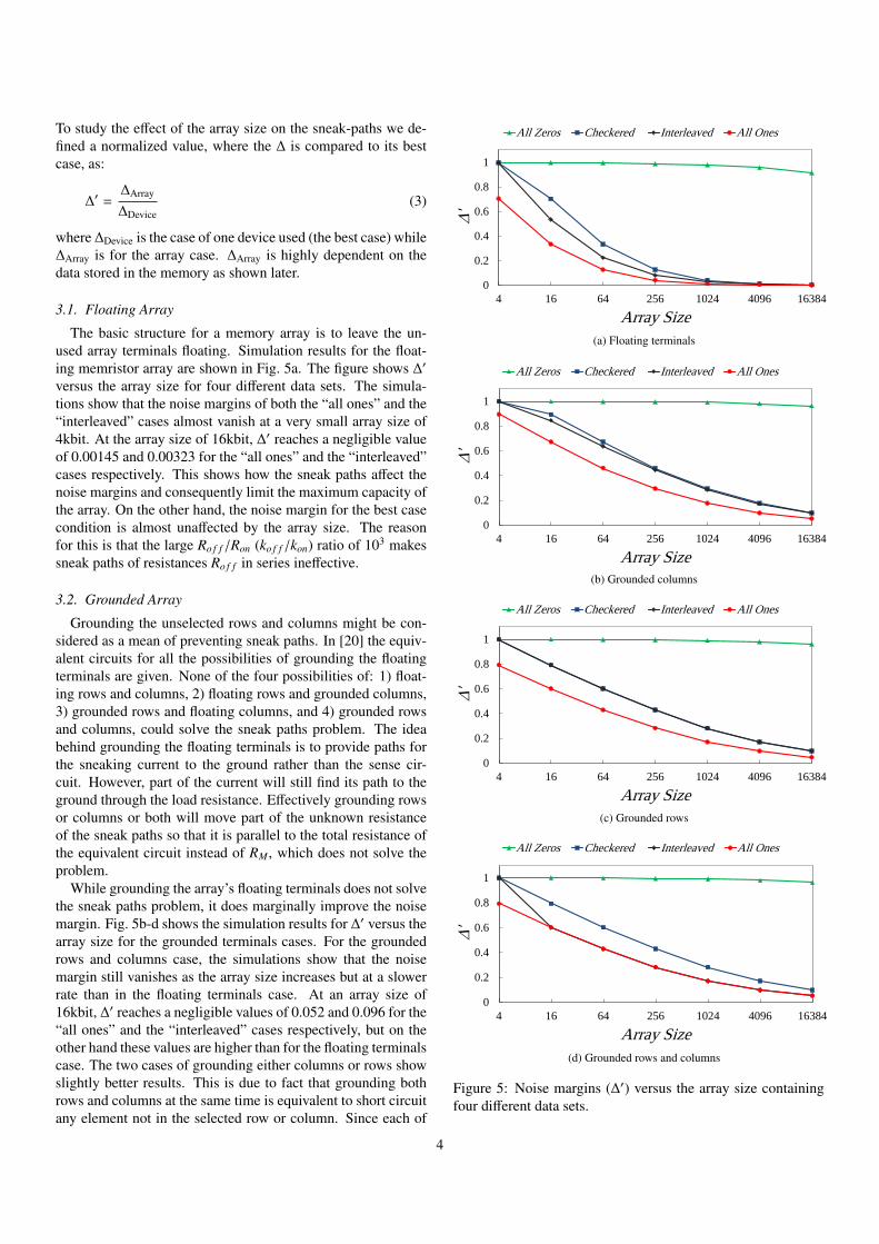
3.1. Floating Array
The basic structure for a memory array is to leave the un-used array terminals floating. Simulation results for the float-ing memristor array are shown in Fig. 5a. The figure shows ∆′
versus the array size for four different data sets. The simula-tions show that the noise margins of both the “all ones” and the“interleaved” cases almost vanish at a very small array size of4kbit. At the array size of 16kbit, ∆′ reaches a negligible valueof 0.00145 and 0.00323 for the “all ones” and the “interleaved”cases respectively. This shows how the sneak paths affect thenoise margins and consequently limit the maximum capacity ofthe array. On the other hand, the noise margin for the best casecondition is almost unaffected by the array size. The reasonfor this is that the large Ro f f /Ron (ko f f /kon) ratio of 103 makessneak paths of resistances Ro f f in series ineffective.
3.2. Grounded Array
Grounding the unselected rows and columns might be con-sidered as a mean of preventing sneak paths. In [20] the equiv-alent circuits for all the possibilities of grounding the floatingterminals are given. None of the four possibilities of: 1) float-ing rows and columns, 2) floating rows and grounded columns,3) grounded rows and floating columns, and 4) grounded rowsand columns, could solve the sneak paths problem. The ideabehind grounding the floating terminals is to provide paths forthe sneaking current to the ground rather than the sense cir-cuit. However, part of the current will still find its path to theground through the load resistance. Effectively grounding rowsor columns or both will move part of the unknown resistanceof the sneak paths so that it is parallel to the total resistance ofthe equivalent circuit instead of RM , which does not solve theproblem.
While grounding the array’s floating terminals does not solvethe sneak paths problem, it does marginally improve the noisemargin. Fig. 5b-d shows the simulation results for ∆′ versus thearray size for the grounded terminals cases. For the groundedrows and columns case, the simulations show that the noisemargin still vanishes as the array size increases but at a slowerrate than in the floating terminals case. At an array size of16kbit, ∆′ reaches a negligible values of 0.052 and 0.096 for the“all ones” and the “interleaved” cases respectively, but on theother hand these values are higher than for the floating terminalscase. The two cases of grounding either columns or rows showslightly better results. This is due to fact that grounding bothrows and columns at the same time is equivalent to short circuitany element not in the selected row or column. Since each of
0
0.2
0.4
0.6
0.8
1
4 16 64 256 1024 4096 16384
Δ'
Array Size
All Zeros Checkered Interleaved All Ones
(a) Floating terminals
0
0.2
0.4
0.6
0.8
1
4 16 64 256 1024 4096 16384
Δ'
Array Size
All Zeros Checkered Interleaved All Ones
(b) Grounded columns
0
0.2
0.4
0.6
0.8
1
4 16 64 256 1024 4096 16384
Δ'
Array Size
All Zeros Checkered Interleaved All Ones
(c) Grounded rows
0
0.2
0.4
0.6
0.8
1
4 16 64 256 1024 4096 16384
Δ'
Array Size
All Zeros Checkered Interleaved All Ones
(d) Grounded rows and columns
Figure 5: Noise margins (∆′) versus the array size containingfour different data sets.
4
0.01
0.1
1
10
4 16 64 256 1024 4096 16384
Pow
er C
onsu
mpti
on/μ
W
Array Size
Floating (All Ones) Floating (checkered)
Grounded (All Ones) Grounded (checkered)
Ideal Case
Figure 6: Power consumption versus array size plotted logarith-mically for the cases of grounded and floating array terminals.The dotted line shows the ideal case without the sneak pathseffect.
these unselected elements two terminals will be connected toground. Therefore, the total resistance of the sneak-path willbe less than the case of grounding either rows or columns sepa-rately.
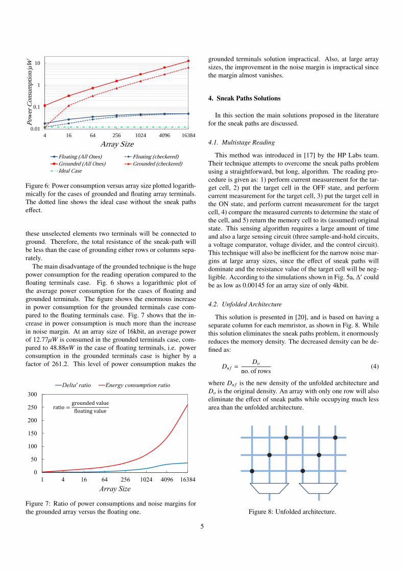
The main disadvantage of the grounded technique is the hugepower consumption for the reading operation compared to thefloating terminals case. Fig. 6 shows a logarithmic plot ofthe average power consumption for the cases of floating andgrounded terminals. The figure shows the enormous increasein power consumption for the grounded terminals case com-pared to the floating terminals case. Fig. 7 shows that the in-crease in power consumption is much more than the increasein noise margin. At an array size of 16kbit, an average powerof 12.77µW is consumed in the grounded terminals case, com-pared to 48.88nW in the case of floating terminals, i.e. powerconsumption in the grounded terminals case is higher by afactor of 261.2. This level of power consumption makes the
0
50
100
150
200
250
300
1 4 16 64 256 1024 4096 16384
Array Size
Delta' ratio Energy consumption ratio
ratio =grounded value
floating value
Figure 7: Ratio of power consumptions and noise margins forthe grounded array versus the floating one.
grounded terminals solution impractical. Also, at large arraysizes, the improvement in the noise margin is impractical sincethe margin almost vanishes.
4. Sneak Paths Solutions
In this section the main solutions proposed in the literaturefor the sneak paths are discussed.
4.1. Multistage Reading
This method was introduced in [17] by the HP Labs team.Their technique attempts to overcome the sneak paths problemusing a straightforward, but long, algorithm. The reading pro-cedure is given as: 1) perform current measurement for the tar-get cell, 2) put the target cell in the OFF state, and performcurrent measurement for the target cell, 3) put the target cell inthe ON state, and perform current measurement for the targetcell, 4) compare the measured currents to determine the state ofthe cell, and 5) return the memory cell to its (assumed) originalstate. This sensing algorithm requires a large amount of timeand also a large sensing circuit (three sample-and-hold circuits,a voltage comparator, voltage divider, and the control circuit).This technique will also be inefficient for the narrow noise mar-gins at large array sizes, since the effect of sneak paths willdominate and the resistance value of the target cell will be neg-ligible. According to the simulations shown in Fig. 5a, ∆′ couldbe as low as 0.00145 for an array size of only 4kbit.
4.2. Unfolded Architecture
This solution is presented in [20], and is based on having aseparate column for each memristor, as shown in Fig. 8. Whilethis solution eliminates the sneak paths problem, it enormouslyreduces the memory density. The decreased density can be de-fined as:
Du f =Do
no. of rows(4)
where Du f is the new density of the unfolded architecture andDo is the original density. An array with only one row will alsoeliminate the effect of sneak paths while occupying much lessarea than the unfolded architecture.
Figure 8: Unfolded architecture.
5
4.3. Diode Gating
One of the proposed solutions for the sneak paths is to adda diode to each memory cell [20], producing a new cell of onediode and one memristor (1D1M), as shown in Fig. 9. Sucha strategy would eliminate sneak paths. According to [44],adding diodes to the array will increase the delay of the sys-tem by adding capacitive loads and diode threshold voltageswill decrease the output swing. However, the major problemfacing such a strategy is that it will block the writing process inthe native array structure, since writing to a memristor requirestwo different polarities. In [45] a 3D array structure is providedto enable the write operation with a diode present. In this tech-nique, each cell will contain one programming element, twodiodes, and four connecting crossbars. While this technique al-lows the write operation, it consumes more area per cell. Inaddition, the 3D alignment for four bars may reduce the arraydensity significantly. Finally, it is not clear that the new struc-ture containing four bars will still eliminate the sneak paths.
4.4. Transistor Gating
Using large transistors for gating the memristor will solvethe sneak paths problem. On the other hand this method willruin the high memristor-memory density, since the gating tran-sistor’s size is much larger than that of the memristor.Althoughusing small devices will reduce the sneak paths it will not elim-inate it. This is due to the fact that the recently introduced smalltransistors are consider to act as leaky valves. Moreover, thesedevices with relatively high OFF current will increase the staticpower component significantly. Finally, it should be mentionedthat one of the major issue of using transistor gating is its limi-tation to the 3D stacking of memristor arrays. In [46] an arrayof one transistor and one memristor (1T1M) is reported. Theyreport a gating transistor of 10µm channel length and 200µmchannel width. Moreover, two wires are required for drivingeach cell; one for the transistor and one for the memristor.
4.5. Complimentary Memristors
In this technique two complimentary memristors are used athe memory cell, so that their total resistance are always “Ron +
Sensing Circuit
Row
Selecto
r
Figure 9: Simple memory array with 1D1M used for each mem-ory cell.
Ro f f ”, as introduced in [47]. Having always a high resistancecell reduces the sneak-path current significantly. In this methodONE is distinguished from the ZERO by the orientation of thedesired cell, Ron, Ro f f or Ro f f , Ron. Therefore, a complexreading technique is required. Moreover, the system will nottake full advantage of having high Ro f f /Ron device.
4.6. Using Memristors NonlinearityThe voltage drop on the desired cell is higher than any of the
sneak-path elements, since the shortest sneak-path will containat least three series memristors. In [48], a high nonlinear deviceis reported, such that I(V/2) ≈ I(V)/100 at V ≈ 1V . This veryuseful property will significantly reduce the sneak paths currentrelative to the desired cell current, and will consistently reducethe sneak-path effect by a high factor. This solution also willnot be practical for large memory array.
4.7. AC SenseInstead of using regular DC signal an AC signal is used for
sensing the data stored in the desired cell, as introduced in [49].This technique uses load capacitance at the input of the senseamplifier to implement a low pass filter, as shown in Fig. 10.The response of the filter is mainly based on the resistive valueof the desired cell. However,this method adds extra complex-ity for the memory system, since AC input and sensing are re-quired. Moreover, this method will not be as effective for largearrays.
Figure 10: Simple memory array showing the added columncapacitors for the AC sense.
5. Array Aspect Ratio
In this section we study the effect of the aspect ratio on theperformance of memristor array. Non-unity aspect ratio couldbe thought of as a helping method towards a sneak-paths freememory. The aspect ratio of an array is defined as its numberof columns to the number of rows. Normal square arrays haveaspect ratios of unity. The aspect ratio of the memory array isone of the main parameters which could be used to limit theeffect of the sneak paths. A memory with one row or one col-umn will not suffer from sneak paths at all, since there will beonly one path for the current as shown in Fig. 11. As the aspectratio approaches unity, the possibilities for sneak paths increaseand ∆′ decreases. An unbalanced aspect ratio structure could
6
8:2 4:4
16:1
Figure 11: Examples of different organizations with differentaspect ratios for a 16-cell memory array.
be fabricated in a square area by folding the array in a zigzagshape. However, the main cost of using an aspect ratio otherthan one is the increase in the required area for selection andsensing circuitry. This area could be given as:
Sense Circuit Area =√
S[θ√
A+ ρ√
A]
(5)
where S is the array size, A is the aspect ratio, θ is the columncell area, and ρ is the row cell area.
0
0.2
0.4
0.6
0.8
1
Δ'
Aspect Ratio
4 16 64 256 1024
(a) Floating terminals
0
0.2
0.4
0.6
0.8
1
Δ'
Aspect Ratio
4 16 64 256 1024
(b) Grounded terminals
Figure 12: Noise margin (∆′) versus aspect ratio for differentarray sizes.
Fig. 12 shows the simulation results for the noise margin ∆′
versus the aspect ratio for different array sizes. The simulationsare made for array structures with both floating and groundedterminals with the “all ones” data set (the worst case). In gen-eral the simulations show that the minimum values for ∆′ occurat an aspect ratio of one. Conversely, the sneak paths effect dis-appears completely for the cases of a one-row or one-columnarray. By comparing Fig. 12a and Fig. 12b we can see that therate of decay of the noise margin with aspect ratio is much fasterin the floating case than the grounded one. For the grounded ar-rays, the noise margin depends mainly on the number of rowsrather than the aspect ratio. This is due to the fact that the cur-rent sneaks mainly through the columns near the active cell,regardless of the total number of columns.
6. Gating Using Three-Terminal Memistor Device
Memristors can be considered better gates compared to tran-sistors or diodes, since they can be characterized by having veryhigh OFF resistance with much smaller area. In [17], memristordevices are reported to have Ro f f = 1GΩ. Moreover, memris-tors are not intruder species to the memory array, compared totransistors and diodes. However, it is not possible to write on ei-ther the gate memristor or the data memristor separately, givena device with high ON/OFF ratios of more than one hundred.Also, trying to introduce extra rows or columns to enable sep-arate writing will return us to the initial point, where the sneakpaths are dominant.
The three-terminal memistor device captures both of theadvantages of the memristor and transistor as a gate device.This device was introduced prior to the memristor in 1960 byWidrow [50]. The memistor is a three-terminal device where
Desired Cell Data Device
ON Memistor OFF Memistor
Figure 13: Structure of the proposed memristor gated array,where an example of selected of selected cell is shown.
7
the resistance between two terminals is controlled using thethird one, in the same analogy of transistor but with a mem-ory effect. In other words, the resistance of the device is con-trolled by time integral of the current on the third terminal andnot the instantaneous current as the case of transistor, as statedbe in [50, 51]. This means that there is no need to keep an ac-tive bias on the third terminal to keep the device ON (or OFF).The memistor will retain is ON or OFF state after removing thebias from the third terminal. One of the advantages of this bias-less switching is the very low static power consumed. Memis-tors can inherent the high ON/OFF ratio and small footprint ofmemristors and the high controllability of transistor by havinga third terminal. Fig. 13 shows the structure of the memistorgated array, where each memory cell is gated with a memis-tor device. Extra columns are required for programming thememistor gate. It is a assumed that the memistor has the sameON/OFF values of the data cell. At the desired cell the gate de-vice is turned ON and all the other gates are turned OFF, whichis how the desired cell is selected. Therefore, all the sneak pathswill contain at least three series high resistances. This will shiftthe operation of the memory to work equivalently to the bestcase scenario, where all the sneak paths are made of OFF de-vices.
All the unselected cells will have a total resistance higherthan Ro f f . The resistance of the selected cell, with open gate,will depend mainly on the data device resistance. This resis-tance will be either 2Ron or Ro f f+Ron, with a very high ON/OFFratio. Our proposed method has a major advantage over thecomplementary memristors technique that the desired cell hasmuch higher ratio between its ON and OFF states. In comple-mentary structures the total resistance is always (Ron +Ro f f ), inall of the cases. Based on that, our proposed solution has higheraverage signal to noise ratio. Moreover, the Ro f f /Ron ratio ofthe device is directly reflected on desired cell state values.
Fig. 14 show the noise margins for the proposed techniqueand the normal array with floating terminals versus the arraysize for the worst case data set “all ones”. It appears clearly thatthe memistor gating has a significant impact on the sneak paths
0
150
300
450
600
0
0.2
0.4
0.6
0.8
1
4 16 64 256 1024 4096 16384
Δ'
Array Size
Memistor Gating Floating Terminals Ratio
Figure 14: Noise margins (∆′) versus the array size for thenormal array with floating terminals and the new introducedmemistor gated array for “All Ones” data set. Also the ratio be-tween the two results are shown in green color on the secondaryaxis.
0
5
10
15
20
25
30
35
40
45
50
4 16 64 256 1024 4096 16384
Po
wer
Co
nsu
mp
tio
n/n
W
Array Size
Floating Terminals (All Ones) Memristor Gating (All Ones)
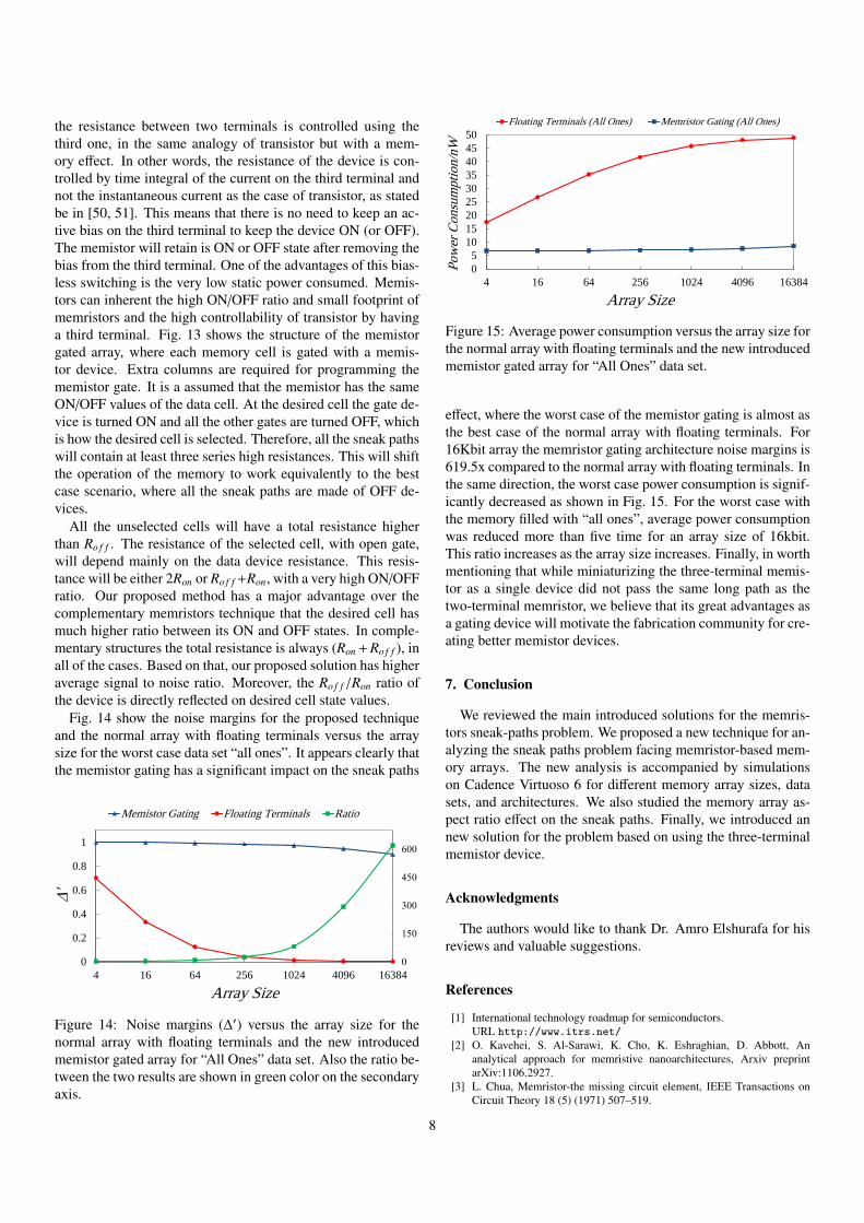
Figure 15: Average power consumption versus the array size forthe normal array with floating terminals and the new introducedmemistor gated array for “All Ones” data set.
effect, where the worst case of the memistor gating is almost asthe best case of the normal array with floating terminals. For16Kbit array the memristor gating architecture noise margins is619.5x compared to the normal array with floating terminals. Inthe same direction, the worst case power consumption is signif-icantly decreased as shown in Fig. 15. For the worst case withthe memory filled with “all ones”, average power consumptionwas reduced more than five time for an array size of 16kbit.This ratio increases as the array size increases. Finally, in worthmentioning that while miniaturizing the three-terminal memis-tor as a single device did not pass the same long path as thetwo-terminal memristor, we believe that its great advantages asa gating device will motivate the fabrication community for cre-ating better memistor devices.
7. Conclusion
We reviewed the main introduced solutions for the memris-tors sneak-paths problem. We proposed a new technique for an-alyzing the sneak paths problem facing memristor-based mem-ory arrays. The new analysis is accompanied by simulationson Cadence Virtuoso 6 for different memory array sizes, datasets, and architectures. We also studied the memory array as-pect ratio effect on the sneak paths. Finally, we introduced annew solution for the problem based on using the three-terminalmemistor device.
Acknowledgments
The authors would like to thank Dr. Amro Elshurafa for hisreviews and valuable suggestions.
References
[1] International technology roadmap for semiconductors.URL http://www.itrs.net/
[2] O. Kavehei, S. Al-Sarawi, K. Cho, K. Eshraghian, D. Abbott, Ananalytical approach for memristive nanoarchitectures, Arxiv preprintarXiv:1106.2927.
[3] L. Chua, Memristor-the missing circuit element, IEEE Transactions onCircuit Theory 18 (5) (1971) 507–519.
8
[4] D. B. Strukov, G. S. Snider, D. R. Stewart, R. S. Williams, The missingmemristor found, Nature 435 (2008) 80–83.
[5] A. Zakhidov, B. Jung, J. Slinker, H. Abruna, G. Malliaras, A light-emitting memristor, Organic Electronics 11 (1) (2010) 150–153.
[6] S. Jo, K. Kim, W. Lu, High-density crossbar arrays based on a si memris-tive system, Nano letters 9 (2) (2009) 870–874.
[7] N. Gergel-Hackett, B. Hamadani, B. Dunlap, J. Suehle, C. Richter,C. Hacker, D. Gundlach, A flexible solution-processed memristor, IEEEElectron Device Letters 30 (7) (2009) 706–708.
[8] R. Waser, Resistive non-volatile memory devices, Microelectronic Engi-neering 86 (7-9) (2009) 1925–1928.
[9] T. Kim, E. Jang, N. Lee, D. Choi, K. Lee, J. Jang, J. Choi, S. Moon,J. Cheon, Nanoparticle assemblies as memristors, Nano letters 9 (6)(2009) 2229–2233.
[10] Z. Biolek, D. Biolek, V. Biolkova, SPICE model of memristor with non-linear dopant drift, Radioengineering 18 (2) (2009) 210–214.
[11] J. Valsa, D. Biolek, Z. Biolek, An analogue model of the memristor, Inter-national Journal of Numerical Modelling: Electronic Networks, Devicesand Fields 24 (4) (2011) 400–408.
[12] A. G. Radwan, M. A. Zidan, K. N. Salama, HP memristor mathematicalmodel for periodic signals and DC, in: IEEE International Midwest Sym-posium on Circuits and Systems (MWSCAS’10), 2010, pp. 861–864.
[13] A. G. Radwan, M. A. Zidan, K. N. Salama, On the mathematical model-ing of memristors, in: IEEE International Conference on Microelectronics(ICM’10), 2010, pp. 284–287.
[14] H. Abdalla, M. Pickett, SPICE modeling of memristors, in: IEEE In-ternational Symposium on Circuits and Systems (ISCAS’11), 2011, pp.1832–1835.
[15] S. Kvatinsky, E. Friedman, A. Kolodny, U. Weiser, Team: Thresholdadaptive memristor model, Submitted to IEEE Transactions on Circuitsand Systems I: Regular Papers, (also CCIT Technical Report #804).
[16] T. Prodromakis, B. Peh, C. Papavassiliou, C. Toumazou, A versatile mem-ristor model with nonlinear dopant kinetics, IEEE transactions on electrondevices 58 (9) (2011) 3099–3105.
[17] P. Vontobel, W. Robinett, P. Kuekes, D. Stewart, J. Straznicky, R. Stan-ley Williams, Writing to and reading from a nano-scale crossbar memorybased on memristors, Nanotechnology 20 (2009) 425204.
[18] Y. Ho, G. Huang, P. Li, Dynamical properties and design analysis for non-volatile memristor memories, IEEE Transactions on Circuits and SystemsI: Regular Papers 58 (4) (2011) 724–736.
[19] K.-H. Jo, C.-M. Jung, K.-S. Min, S.-M. Kang, Self-adaptive write circuitfor low-power and variation-tolerant memristors, IEEE Transactions onNanotechnology 9 (6) (2010) 675–678.
[20] H. Manem, G. Rose, X. He, W. Wang, Design considerations for variationtolerant multilevel cmos/nano memristor memory, in: Proceedings of the20th symposium on Great lakes symposium on VLSI, 2010, pp. 287–292.
[21] Y. Pershin, M. Di Ventra, Experimental demonstration of associativememory with memristive neural networks, Neural Networks 23 (7) (2010)881–886.
[22] K. Eshraghian, K. Cho, O. Kavehei, S. Kang, D. Abbott, S. Kang, Mem-ristor MOS content addressable memory (MCAM): Hybrid architecturefor future high performance search engines, IEEE Transactions on VeryLarge Scale Integration (VLSI) Systems (99) (2010) 1–11.
[23] D. Niu, Y. Chen, Y. Xie, Low-power dual-element memristor based mem-ory design, in: The 16th ACM/IEEE international symposium on Lowpower electronics and design, 2010, pp. 25–30.
[24] Y. V. Pershin, M. D. Ventra, Experimental demonstration of associativememory with memristive neural networks, Neural Networks 23 (7) (2010)881–886.
[25] P. O. Vontobel, W. Robinett, P. J. Kuekes, D. R. Stewart, J. Straznicky,R. S. Williams, Writing to and reading from a nano-scale crossbar mem-ory based on memristors, Nanotechnology 20 (42) (2009) 425204.
[26] G. Huang, Y. Ho, P. Li, Memristor system properties and its design ap-plications to circuits such as nonvolatile memristor memories, in: In-ternational Conference on Communications, Circuits and Systems (IC-
CCAS’10), 2010, pp. 805–810.[27] A. Talukdar, A. G. Radwan, K. N. Salama, Generalized model for
memristor-based wien family oscillators, Microelectronics Journal 42 (9)(2011) 1032–1038.
[28] A. Talukdar, A. G. Radwan, K. N. Salama, Non linear dynamics of mem-ristor based 3rd order oscillatory system, Microelectronics Journal 43 (3)(2012) 169–175.
[29] M. A. Zidan, H. Omran, A. G. Radwan, K. N. Salama, Memristor-basedreactance-less oscillator, Electronics Letters 47 (22) (2011) 1220–1221.
[30] M. Itoh, L. Chua, Memristor oscillators, Int. J. Bifurcation and Chaos18 (11) (2008) 3183–3206.
[31] W. Robinett, M. Pickett, J. Borghetti, Q. Xia, G. Snider, G. Medeiros-Ribeiro, R. Williams, A memristor-based nonvolatile latch circuit, Nan-otechnology 21 (2010) 235203.
[32] F. Merrikh-Bayat, S. Shouraki, Memristor-based circuits for performingbasic arithmetic operations, Procedia Computer Science 3 (2011) 128–132.
[33] S. Shin, K. Kim, S.-M. Kang, Memristor applications for programmableanalog ics, IEEE Transactions on Nanotechnology 10 (2) (2011) 266–274.
[34] Y. Pershin, M. Di Ventra, Practical approach to programmable analogcircuits with memristors, IEEE Transactions on Circuits and Systems I:Regular Papers 57 (8) (2010) 1857–1864.
[35] Y. V. Pershin, S. La Fontaine, M. Di Ventra, Memristive model of amoebalearning, Physical Review E 80 (2) (2009) 021926.
[36] S. Jo, T. Chang, I. Ebong, B. Bhadviya, P. Mazumder, W. Lu, Nanoscalememristor device as synapse in neuromorphic systems, Nano letters 10 (4)(2010) 1297–1301.
[37] M. Kryder, C. Kim, After hard drives-what comes next?, IEEE Transac-tions on Magnetics 45 (10) (2009) 3406–3413.
[38] F. Miao, J. P. Strachan, J. J. Yang, M.-X. Zhang, I. Goldfarb, A. C. Tor-rezan, P. Eschbach, R. D. Kelley, G. Medeiros-Ribeiro, R. S. Williams,Anatomy of a nanoscale conduction channel reveals the mechanism of ahigh-performance memristor, Advanced Materials 23 (2011) 5633–5640.
[39] Elpida Memory develops resistance RAM prototype.URL http://www.elpida.com/en/news/2012/01-24r.html
[40] L. Chua, Resistance switching memories are memristors, Applied PhysicsA: Materials Science & Processing 102 (4) (2011) 765–783.
[41] D. Manners, IEF2011: HP to replace flash and SSD in 2013, ElectronicsWeekly (2011).
[42] G. Rose, Overview: Memristive devices, circuits and systems, in: IEEEInternational Symposium on Circuits and Systems (ISCAS’10), 2010, pp.1955–1958.
[43] S.-M. Kang, Y. Leblebici, CMOS Digital Integrated Circuits Analysis &Design, McGraw-Hill, 2007.
[44] W. Fei, H. Yu, W. Zhang, K. Yeo, Design exploration of hybrid cmos andmemristor circuit by new modified nodal analysis, IEEE Transactions onVery Large Scale Integration (VLSI) Systems (99) (2011) 1–15.
[45] B. Mouttet, Programmable crossbar signal processor, US Patent7,302,513 (2007).
[46] S. Kim, H. Jeong, S. Kim, S. Choi, K. Lee, Flexible memristive memoryarray on plastic substrates, Nano Letters 11 (12) (2011) 5438–5442.
[47] C. Jung, J. Choi, K. Min, Two-step write scheme for reducing sneak-path leakage in complementary memristor array, IEEE Transactions onNanotechnology 11 (3) (2012) 611–618.
[48] J. J. Yang, M.-X. Zhang, M. D. Pickett, F. Miao, J. P. Strachan, W.-D. Li,W. Yi, D. A. A. Ohlberg, B. J. Choi, W. Wu, J. H. Nickel, G. Medeiros-Ribeiro, R. S. Williams, Engineering nonlinearity into memristors forpassive crossbar applications, Applied Physics Letters 100 (11) (2012)113501.
[49] M. Qureshi, W. Yi, G. Medeiros-Ribeiro, R. Williams, AC sense tech-nique for memristor crossbar, Electronics letters 48 (13) (2012) 757–758.
[50] B. Widrow, Adaptive “adaline” neuron using chemical “memistors”,Tech. rep., Stanford University (1960).
[51] H. Kim, S. Adhikari, Memistor is not memristor, IEEE Circuits and Sys-tems Magazine 12 (1) (2012) 75–78.
9


![Modeling of the Memristor in SPICE Introduction In 1971, professor Chua predicted the existence of the fourth circuit element – memristor [3]. The memristor](https://img.pdfslide.us/doc/110x75/56649e3b5503460f94b2d7a3/modeling-of-the-memristor-in-spice-introduction-in-1971-professor-chua-predicted.jpg)


![Memristor Seminar Report[1]](https://img.pdfslide.us/doc/110x75/577d1f3c1a28ab4e1e9029c7/memristor-seminar-report1.jpg)