Embed Size (px)
Citation preview
© Semiconductor Components Industries, LLC, 2013
August, 2013 − Rev. 141 Publication Order Number:
MC34262/D
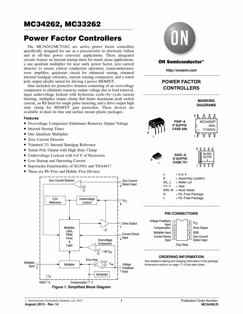
MC34262, MC33262
Power Factor ControllersThe MC34262/MC33262 are active power factor controllers
specifically designed for use as a preconverter in electronic ballastand in off−line power converter applications. These integratedcircuits feature an internal startup timer for stand−alone applications,a one quadrant multiplier for near unity power factor, zero currentdetector to ensure critical conduction operation, transconductanceerror amplifier, quickstart circuit for enhanced startup, trimmedinternal bandgap reference, current sensing comparator, and a totempole output ideally suited for driving a power MOSFET.
Also included are protective features consisting of an overvoltagecomparator to eliminate runaway output voltage due to load removal,input undervoltage lockout with hysteresis, cycle−by−cycle currentlimiting, multiplier output clamp that limits maximum peak switchcurrent, an RS latch for single pulse metering, and a drive output highstate clamp for MOSFET gate protection. These devices areavailable in dual−in−line and surface mount plastic packages.
Features• Overvoltage Comparator Eliminates Runaway Output Voltage• Internal Startup Timer• One Quadrant Multiplier• Zero Current Detector• Trimmed 2% Internal Bandgap Reference• Totem Pole Output with High State Clamp• Undervoltage Lockout with 6.0 V of Hysteresis• Low Startup and Operating Current• Supersedes Functionality of SG3561 and TDA4817• These are Pb−Free and Halide−Free Devices
Figure 1. Simplified Block Diagram
VoltageFeedbackInput
Multiplier,Latch,PWM,Timer,
&Logic
Error Amp
Multiplier
UndervoltageLockout
2.5VReference
Zero Current Detector
5
8
6
7
4
3
2
1
Drive Output
GND
Zero CurrentDetect Input
MultiplierInput
Compensation
VCC
Current SenseInput
OvervoltageComparator
+1.08 Vref
+Vref
Quickstart
POWER FACTORCONTROLLERS
PIN CONNECTIONS
SOIC−8D SUFFIXCASE 751
81
81
PDIP−8P SUFFIXCASE 626
Voltage FeedbackInput 1
2
3
4
8
7
6
5
(Top View)
Compensation
Multiplier InputCurrent Sense
Input
VCC
Drive Output
GNDZero CurrentDetect Input
http://onsemi.com
See detailed ordering and shipping information in the packagedimensions section on page 17 of this data sheet.
ORDERING INFORMATION
x = 3 or 4A = Assembly LocationWL, L = Wafer LotYY, Y = YearWW, W = Work WeekG = Pb−Free Package� = Pb−Free Package
MARKINGDIAGRAMS
MC3x262PAWL
YYWWG
1
8
3x262ALYW
�
1
8
MC34262, MC33262
http://onsemi.com2
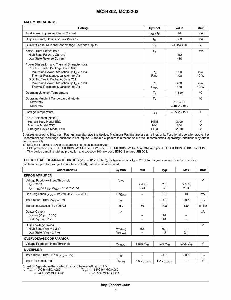
MAXIMUM RATINGS
Rating Symbol Value Unit
Total Power Supply and Zener Current (ICC + IZ) 30 mA
Output Current, Source or Sink (Note 1) IO 500 mA
Current Sense, Multiplier, and Voltage Feedback Inputs Vin −1.0 to +10 V
Zero Current Detect InputHigh State Forward CurrentLow State Reverse Current
Iin 50−10
mA
Power Dissipation and Thermal CharacteristicsP Suffix, Plastic Package, Case 626
Maximum Power Dissipation @ TA = 70°CThermal Resistance, Junction−to−Air
D Suffix, Plastic Package, Case 751Maximum Power Dissipation @ TA = 70°CThermal Resistance, Junction−to−Air
PDR�JA
PDR�JA
800100
450178
mW°C/W
mW°C/W
Operating Junction Temperature TJ +150 °C
Operating Ambient Temperature (Note 4)MC34262MC33262
TA0 to + 85
− 40 to +105
°C
Storage Temperature Tstg − 65 to +150 °C
ESD Protection (Note 2)Human Body Model ESDMachine Model ESDCharged Device Model ESD
HBMMM
CDM
20002002000
VVV
Stresses exceeding Maximum Ratings may damage the device. Maximum Ratings are stress ratings only. Functional operation above theRecommended Operating Conditions is not implied. Extended exposure to stresses above the Recommended Operating Conditions may affectdevice reliability.1. Maximum package power dissipation limits must be observed.2. ESD protection per JEDEC JESD22−A114−F for HBM, per JEDEC JESD22−A115−A for MM, and per JEDEC JESD22−C101D for CDM.
This device contains latchup protection and exceeds 100 mA per JEDEC Standard JESD78.
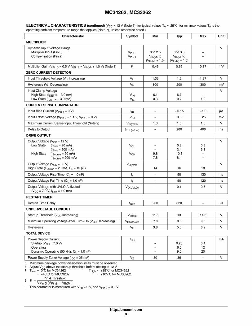
ELECTRICAL CHARACTERISTICS (VCC = 12 V (Note 3), for typical values TA = 25°C, for min/max values TA is the operatingambient temperature range that applies (Note 4), unless otherwise noted.)
Characteristic Symbol Min Typ Max Unit
ERROR AMPLIFIER
Voltage Feedback Input ThresholdTA = 25°CTA = Tlow to Thigh (VCC = 12 V to 28 V)
VFB2.4652.44
2.5−
2.5352.54
V
Line Regulation (VCC = 12 V to 28 V, TA = 25°C) Regline − 1.0 10 mV
Input Bias Current (VFB = 0 V) IIB − − 0.1 − 0.5 �A
Transconductance (TA = 25°C) gm 80 100 130 �mho
Output CurrentSource (VFB = 2.3 V)Sink (VFB = 2.7 V)
IO−−
1010
−−
�A
Output Voltage SwingHigh State (VFB = 2.3 V)Low State (VFB = 2.7 V)
VOH(ea)VOL(ea)
5.8−
6.41.7
−2.4
V
OVERVOLTAGE COMPARATOR
Voltage Feedback Input Threshold VFB(OV) 1.065 VFB 1.08 VFB 1.095 VFB V
MULTIPLIER
Input Bias Current, Pin 3 (VFB = 0 V) IIB − − 0.1 − 0.5 �A
Input Threshold, Pin 2 Vth(M) 1.05 VOL(EA) 1.2 VOL(EA) − V
3. Adjust VCC above the startup threshold before setting to 12 V.4. Tlow = 0°C for MC34262 Thigh = +85°C for MC34262
= −40°C for MC33262 = +105°C for MC33262.
MC34262, MC33262
http://onsemi.com3
ELECTRICAL CHARACTERISTICS (continued) (VCC = 12 V (Note 6), for typical values TA = 25°C, for min/max values TA is theoperating ambient temperature range that applies (Note 7), unless otherwise noted.)
Characteristic Symbol Min Typ Max Unit
MULTIPLIER
Dynamic Input Voltage RangeMultiplier Input (Pin 3)Compensation (Pin 2)
VPin 3VPin 2
0 to 2.5Vth(M) to
(Vth(M) + 1.0)
0 to 3.5Vth(M) to
(Vth(M) + 1.5)
−−
V
Multiplier Gain (VPin 3 = 0.5 V, VPin 2 = Vth(M) + 1.0 V) (Note 8) K 0.43 0.65 0.87 1/V
ZERO CURRENT DETECTOR
Input Threshold Voltage (Vin Increasing) Vth 1.33 1.6 1.87 V
Hysteresis (Vin Decreasing) VH 100 200 300 mV
Input Clamp VoltageHigh State (IDET = + 3.0 mA)Low State (IDET = − 3.0 mA)
VIHVIL
6.10.3
6.70.7
−1.0
V
CURRENT SENSE COMPARATOR
Input Bias Current (VPin 4 = 0 V) IIB − − 0.15 −1.0 �A
Input Offset Voltage (VPin 2 = 1.1 V, VPin 3 = 0 V) VIO − 9.0 25 mV
Maximum Current Sense Input Threshold (Note 9) Vth(max) 1.3 1.5 1.8 V
Delay to Output tPHL(in/out) − 200 400 ns
DRIVE OUTPUT
Output Voltage (VCC = 12 V)Low State (ISink = 20 mA)Low State (ISink = 200 mA)High State (ISource = 20 mA)High State (ISource = 200 mA)
VOL
VOH
−−
9.87.8
0.32.410.38.4
0.83.3−−
V
Output Voltage (VCC = 30 V)High State (ISource = 20 mA, CL = 15 pF)
VO(max)14 16 18
V
Output Voltage Rise Time (CL = 1.0 nF) tr − 50 120 ns
Output Voltage Fall Time (CL = 1.0 nF) tf − 50 120 ns
Output Voltage with UVLO Activated(VCC = 7.0 V, ISink = 1.0 mA)
VO(UVLO) − 0.1 0.5 V
RESTART TIMER
Restart Time Delay tDLY 200 620 − �s
UNDERVOLTAGE LOCKOUT
Startup Threshold (VCC Increasing) Vth(on) 11.5 13 14.5 V
Minimum Operating Voltage After Turn−On (VCC Decreasing) VShutdown 7.0 8.0 9.0 V
Hysteresis VH 3.8 5.0 6.2 V
TOTAL DEVICE
Power Supply CurrentStartup (VCC = 7.0 V)OperatingDynamic Operating (50 kHz, CL = 1.0 nF)
ICC−−−
0.256.59.0
0.41220
mA
Power Supply Zener Voltage (ICC = 25 mA) VZ 30 36 − V
5. Maximum package power dissipation limits must be observed.6. Adjust VCC above the startup threshold before setting to 12 V.7. Tlow = 0°C for MC34262 Thigh = +85°C for MC34262
= −40°C for MC33262 = +105°C for MC33262.
8. K �Pin 4 Threshold
VPin 3 (VPin2 � Vth(M))9. This parameter is measured with VFB = 0 V, and VPin 3 = 3.0 V.
MC34262, MC33262
http://onsemi.com4
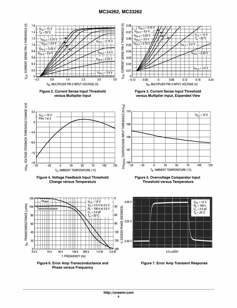
1.4-�0.2 3.80.6 2.2 3.0
VPin 2 = 2.0 V
VCC = 12 VTA = 25°C
VM, MULTIPLIER PIN 3 INPUT VOLTAGE (V)
Figure 2. Current Sense Input Thresholdversus Multiplier Input
-�0.12VM, MULTIPLIER PIN 3 INPUT VOLTAGE (V)
-�0.06 0.06 0.12 0.18 0.240
VCC = 12 VTA = 25°C
Figure 3. Current Sense Input Thresholdversus Multiplier Input, Expanded View
0.2
0
1.6 0.08
1.4
1.2
1.0
0.8
0.6
0.4
0.07
0.06
0.05
0.04
0.03
0.02
0.01
0
VPin 2 = 3.75 V
VPin 2 = 2.25 V
VPin 2 = 2.5 V
VPin 2 = 2.75 V
VPin 2 = 3.0 V VPin 2 = 2.25 V
VPin 2 = 2.5 V
VPin 2 = 3.75 V
VPin 2 = 2.75 V
VPin 2 = 2.0 V
VPin 2 = 3.25 V
VPin 2 = 3.0 VVPin 2 = 3.25 VVPin 2 = 3.5 V
VPin 2 = 3.5 V
Figure 4. Voltage Feedback Input ThresholdChange versus Temperature
Figure 5. Overvoltage Comparator Input Threshold versus Temperature
VCC = 12 V
-�55
TA, AMBIENT TEMPERATURE (°C)
-�25 0 25 50 75 100
Figure 6. Error Amp Transconductance andPhase versus Frequency
-�55
TA, AMBIENT TEMPERATURE (°C)
-�25 0 25 50 75 100 125
VCC = 12 V Pins 1 to 2
Figure 7. Error Amp Transient Response
125
3.0 k 10 k 30 k 100 k 300 k 1.0 M 3.0 M
0
90
60
30
120
150
180
f, FREQUENCY (Hz)
VCC = 12 VVO = 2.5 V to 3.5 VRL = 100 k to 3.0 VCL = 2.0 pFTA = 25°C
5.0 �s/DIV
Transconductance
Phase
0V/
DIV
VCC = 12 VRL = 100 kCL = 2.0 pFTA = 25°C
110
109
108
106
107
�4.0
-�4.0
-12
-16
0
-�8.0
120
100
80
60
40
20
0
4.00 V
3.25 V
2.50 V
�V F
B, V
OLT
AGE
FEED
BAC
K TH
RES
HO
LD C
HAN
GE
(mV)
V CS,
CU
RR
ENT
SEN
SE P
IN 4
TH
RES
HO
LD (V
)
V CS,
CU
RR
ENT
SEN
SE P
IN 4
TH
RES
HO
LD (V
)�
V FB(
OV)
, OVE
RVO
LTAG
E IN
PUT
THR
ESH
OLD
(%V F
B)
g m, T
RAN
SCO
ND
UC
TAN
CE
(�m
ho)
�, E
XCES
S PH
ASE
(DEG
REE
S)
MC34262, MC33262
http://onsemi.com5
-�55TA, AMBIENT TEMPERATURE (°C)
-�25 0 25 50 75 100 125
VCC = 12 V
Figure 8. Quickstart Charge Current versus Temperature
Figure 9. Restart Timer Delay versus Temperature
TA, AMBIENT TEMPERATURE (°C)
-�55 -�25 0 25 50 75 100 125
CurrentVoltage
900
800
700
600
500
VCC = 12 V800
700
600
500
400
1.80
1.76
1.72
1.68
1.64
Figure 10. Zero Current Detector InputThreshold Voltage versus Temperature
Figure 11. Output Saturation Voltageversus Load Current
0 80 160 240 320
IO, OUTPUT LOAD CURRENT (mA)-�55
TA, AMBIENT TEMPERATURE (°C)-�25 0 25 50 75 100 125
VCC = 12 VVCC
GND
0
-�2.0
-�4.0
-�6.0
2.0
0
4.0
1.7
1.5
1.3
1.6
1.4
Upper Threshold(Vin, Increasing)
Lower Threshold(Vin, Decreasing)
Source Saturation(Load to Ground)
Sink Saturation(Load to VCC)
VCC = 12 V 80 �s Pulsed Load120 Hz Rate
VCC = 12 VCL = 1.0 nFTA = 25°C
VCC = 12 VCL = 15 pFTA = 25°C
5.0
V/D
IV10
0m
A/D
IV
100 ns/DIV 100 ns/DIVI CC
, SU
PPLY
CU
RR
ENT
V O, O
UTP
UT
VOLT
AGE
Figure 12. Drive Output Waveform Figure 13. Drive Output Cross Conduction
90%
10%
V chg
, QU
ICKS
TAR
T C
HAR
GE
VOLT
AGE
(V)
I chg,
QU
ICKS
TAR
T C
HAR
GE
CU
RR
ENT
(�A)
t DLY
, RES
TAR
T TI
ME
DEL
AY (�
s)V s
at, O
UTP
UT
SATU
RAT
ION
VO
LTAG
E (V
)
V th,
TH
RES
HO
LD V
OLT
AGE
(V)
MC34262, MC33262
http://onsemi.com6
I CC
, SU
PPLY
CU
RR
ENT
(mA)
0 10 20 30 40
VCC, SUPPLY VOLTAGE (V)
VFB = 0 VCurrent Sense = 0 VMultiplier = 0 VCL = 1.0 nFf = 50 kHzTA = 25°C
-�55 -�25 0 25 50 75 100 125
TA, AMBIENT TEMPERATURE (°C)
V CC
, SU
PPLY
VO
LTAG
E (V
)
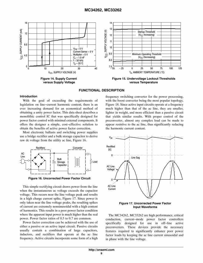
Figure 14. Supply Current versus Supply Voltage
Figure 15. Undervoltage Lockout Thresholdsversus Temperature
Startup Threshold(VCC Increasing)
16
12
8.0
4.0
0
14
13
12
11
9.0
7.0
8.0
10
Minimum Operating Threshold(VCC Decreasing)
FUNCTIONAL DESCRIPTION
IntroductionWith the goal of exceeding the requirements of
legislation on line−current harmonic content, there is anever increasing demand for an economical method ofobtaining a unity power factor. This data sheet describes amonolithic control IC that was specifically designed forpower factor control with minimal external components. Itoffers the designer a simple, cost−effective solution toobtain the benefits of active power factor correction.
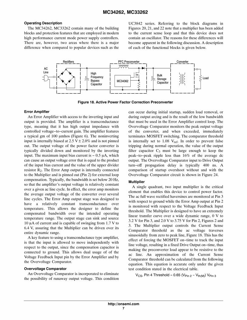
Most electronic ballasts and switching power suppliesuse a bridge rectifier and a bulk storage capacitor to deriveraw dc voltage from the utility ac line, Figure 16.
Figure 16. Uncorrected Power Factor Circuit
ACLine
Rectifiers Converter
BulkStorageCapacitor
+ Load
This simple rectifying circuit draws power from the linewhen the instantaneous ac voltage exceeds the capacitorvoltage. This occurs near the line voltage peak and resultsin a high charge current spike, Figure 17. Since power isonly taken near the line voltage peaks, the resulting spikesof current are extremely nonsinusoidal with a high contentof harmonics. This results in a poor power factor conditionwhere the apparent input power is much higher than the realpower. Power factor ratios of 0.5 to 0.7 are common.
Power factor correction can be achieved with the use ofeither a passive or an active input circuit. Passive circuitsusually contain a combination of large capacitors,inductors, and rectifiers that operate at the ac linefrequency. Active circuits incorporate some form of a high
frequency switching converter for the power processing,with the boost converter being the most popular topology,Figure 18. Since active input circuits operate at a frequencymuch higher than that of the ac line, they are smaller,lighter in weight, and more efficient than a passive circuitthat yields similar results. With proper control of thepreconverter, almost any complex load can be made toappear resistive to the ac line, thus significantly reducingthe harmonic current content.
Figure 17. Uncorrected Power FactorInput Waveforms
Vpk
Rectified
0
AC LineVoltage
0
AC LineCurrent
Line Sag
DC
The MC34262, MC33262 are high performance, criticalconduction, current−mode power factor controllersspecifically designed for use in off−line activepreconverters. These devices provide the necessaryfeatures required to significantly enhance poor powerfactor loads by keeping the ac line current sinusoidal andin phase with the line voltage.
MC34262, MC33262
http://onsemi.com7
Operating DescriptionThe MC34262, MC33262 contain many of the building
blocks and protection features that are employed in modernhigh performance current mode power supply controllers.There are, however, two areas where there is a majordifference when compared to popular devices such as the
UC3842 series. Referring to the block diagrams inFigures 20, 21, and 22 note that a multiplier has been addedto the current sense loop and that this device does notcontain an oscillator. The reasons for these differences willbecome apparent in the following discussion. A descriptionof each of the functional blocks is given below.
Figure 18. Active Power Factor Correction Preconverter
Rectifiers PFC Preconverter
HighFrequencyBypassCapacitor
+
Converter
BulkStorageCapacitor
+ LoadMC34362
ACLine
Error AmplifierAn Error Amplifier with access to the inverting input and
output is provided. The amplifier is a transconductancetype, meaning that it has high output impedance withcontrolled voltage−to−current gain. The amplifier featuresa typical gm of 100 �mhos (Figure 6). The noninvertinginput is internally biased at 2.5 V ± 2.0% and is not pinnedout. The output voltage of the power factor converter istypically divided down and monitored by the invertinginput. The maximum input bias current is − 0.5 �A, whichcan cause an output voltage error that is equal to the productof the input bias current and the value of the upper dividerresistor R2. The Error Amp output is internally connectedto the Multiplier and is pinned out (Pin 2) for external loopcompensation. Typically, the bandwidth is set below 20 Hz,so that the amplifier’s output voltage is relatively constantover a given ac line cycle. In effect, the error amp monitorsthe average output voltage of the converter over severalline cycles. The Error Amp output stage was designed tohave a relatively constant transconductance overtemperature. This allows the designer to define thecompensated bandwidth over the intended operatingtemperature range. The output stage can sink and source10 �A of current and is capable of swinging from 1.7 V to6.4 V, assuring that the Multiplier can be driven over itsentire dynamic range.
A key feature to using a transconductance type amplifier,is that the input is allowed to move independently withrespect to the output, since the compensation capacitor isconnected to ground. This allows dual usage of of theVoltage Feedback Input pin by the Error Amplifier and bythe Overvoltage Comparator.
Overvoltage ComparatorAn Overvoltage Comparator is incorporated to eliminate
the possibility of runaway output voltage. This condition
can occur during initial startup, sudden load removal, orduring output arcing and is the result of the low bandwidththat must be used in the Error Amplifier control loop. TheOvervoltage Comparator monitors the peak output voltageof the converter, and when exceeded, immediatelyterminates MOSFET switching. The comparator thresholdis internally set to 1.08 Vref. In order to prevent falsetripping during normal operation, the value of the outputfilter capacitor C3 must be large enough to keep thepeak−to−peak ripple less than 16% of the average dcoutput. The Overvoltage Comparator input to Drive Outputturn−off propagation delay is typically 400 ns. Acomparison of startup overshoot without and with theOvervoltage Comparator circuit is shown in Figure 24.
MultiplierA single quadrant, two input multiplier is the critical
element that enables this device to control power factor.The ac full wave rectified haversines are monitored at Pin 3with respect to ground while the Error Amp output at Pin 2is monitored with respect to the Voltage Feedback Inputthreshold. The Multiplier is designed to have an extremelylinear transfer curve over a wide dynamic range, 0 V to3.2 V for Pin 3, and 2.0 V to 3.75 V for Pin 2, Figures 2 and3. The Multiplier output controls the Current SenseComparator threshold as the ac voltage traversessinusoidally from zero to peak line, Figure 18. This has theeffect of forcing the MOSFET on−time to track the inputline voltage, resulting in a fixed Drive Output on−time, thusmaking the preconverter load appear to be resistive to theac line. An approximation of the Current SenseComparator threshold can be calculated from the followingequation. This equation is accurate only under the giventest condition stated in the electrical table.
VCS, Pin 4 Threshold ≈ 0.65 (VPin 2 − Vth(M)) VPin 3
MC34262, MC33262
http://onsemi.com8
A significant reduction in line current distortion can beattained by forcing the preconverter to switch as the ac linevoltage crosses through zero. The forced switching isachieved by adding a controlled amount of offset to theMultiplier and Current Sense Comparator circuits. Theequation shown below accounts for the built−in offsets andis accurate to within ten percent. Let Vth(M) = 1.991 V
VCS, Pin 4 Threshold = 0.544 (VPin 2 − Vth(M)) VPin 3 + 0.0417 (VPin 2 − Vth(M))
Zero Current DetectorThe MC34262 operates as a critical conduction current
mode controller, whereby output switch conduction isinitiated by the Zero Current Detector and terminated whenthe peak inductor current reaches the threshold levelestablished by the Multiplier output. The Zero CurrentDetector initiates the next on−time by setting the RS Latchat the instant the inductor current reaches zero. This criticalconduction mode of operation has two significant benefits.First, since the MOSFET cannot turn−on until the inductorcurrent reaches zero, the output rectifier reverse recoverytime becomes less critical, allowing the use of aninexpensive rectifier. Second, since there are no deadtimegaps between cycles, the ac line current is continuous, thuslimiting the peak switch to twice the average input current.
The Zero Current Detector indirectly senses the inductorcurrent by monitoring when the auxiliary winding voltagefalls below 1.4 V. To prevent false tripping, 200 mV ofhysteresis is provided. Figure 10 shows that the thresholdsare well−defined over temperature. The Zero CurrentDetector input is internally protected by two clamps. Theupper 6.7 V clamp prevents input overvoltage breakdownwhile the lower 0.7 V clamp prevents substrate injection.Current limit protection of the lower clamp transistor isprovided in the event that the input pin is accidentallyshorted to ground. The Zero Current Detector input toDrive Output turn−on propagation delay is typically 320 ns.
Figure 19. Inductor Current and MOSFETGate Voltage Waveforms
Inductor Current Average
MOSFETQ1
On
Off
0
Peak
Current Sense Comparator and RS LatchThe Current Sense Comparator RS Latch configuration
used ensures that only a single pulse appears at the DriveOutput during a given cycle. The inductor current isconverted to a voltage by inserting a ground−referencedsense resistor R7 in series with the source of output switchQ1. This voltage is monitored by the Current Sense Inputand compared to a level derived from the Multiplier output.The peak inductor current under normal operatingconditions is controlled by the threshold voltage of Pin 4where:
Pin 4 ThresholdR7
IL(pk ) =
Abnormal operating conditions occur duringpreconverter startup at extremely high line or if outputvoltage sensing is lost. Under these conditions, theMultiplier output and Current Sense threshold will beinternally clamped to 1.5 V. Therefore, the maximum peakswitch current is limited to:
1.5 VR7
Ipk(max) =
An internal RC filter has been included to attenuate anyhigh frequency noise that may be present on the currentwaveform. This filter helps reduce the ac line currentdistortion especially near the zero crossings. With thecomponent values shown in Figure 21, the Current SenseComparator threshold, at the peak of the haversine variesfrom 1.1 V at 90 Vac to 100 mV at 268 Vac. The CurrentSense Input to Drive Output turn−off propagation delay istypically less than 200 ns.
TimerA watchdog timer function was added to the IC to
eliminate the need for an external oscillator when used instand−alone applications. The Timer provides a means toautomatically start or restart the preconverter if the DriveOutput has been off for more than 620 �s after the inductorcurrent reaches zero. The restart time delay versustemperature is shown in Figure 9.
Undervoltage Lockout and QuickstartAn Undervoltage Lockout comparator has been
incorporated to guarantee that the IC is fully functionalbefore enabling the output stage. The positive powersupply terminal (VCC) is monitored by the UVLOcomparator with the upper threshold set at 13 V and thelower threshold at 8.0 V. In the stand−by mode, with VCCat 7.0 V, the required supply current is less than 0.4 mA.This large hysteresis and low startup current allow theimplementation of efficient bootstrap startup techniques,making these devices ideally suited for wide input rangeoff−line preconverter applications. An internal 36 Vclamp has been added from VCC to ground to protect the ICand capacitor C4 from an overvoltage condition. Thisfeature is desirable if external circuitry is used to delay thestartup of the preconverter. The supply current, startup, andoperating voltage characteristics are shown in Figures 14and 15.

MC34262, MC33262
http://onsemi.com9
A Quickstart circuit has been incorporated to optimizeconverter startup. During initial startup, compensationcapacitor C1 will be discharged, holding the error ampoutput below the Multiplier threshold. This will preventDrive Output switching and delay bootstrapping ofcapacitor C4 by diode D6. If Pin 2 does not reach themultiplier threshold before C4 discharges below the lowerUVLO threshold, the converter will “hiccup” andexperience a significant startup delay. The Quickstartcircuit is designed to precharge C1 to 1.7 V, Figure 8. Thislevel is slightly below the Pin 2 Multiplier threshold,allowing immediate Drive Output switching and bootstrapoperation when C4 crosses the upper UVLO threshold.
Drive OutputThe MC34262/MC33262 contain a single totem−pole
output stage specifically designed for direct drive of power
MOSFETs. The Drive Output is capable of up to ±500 mApeak current with a typical rise and fall time of 50 ns witha 1.0 nF load. Additional internal circuitry has been addedto keep the Drive Output in a sinking mode whenever theUndervoltage Lockout is active. This characteristiceliminates the need for an external gate pulldown resistor.The totem−pole output has been optimized to minimizecross−conduction current during high speed operation. Theaddition of two 10�� resistors, one in series with the sourceoutput transistor and one in series with the sink outputtransistor, helps to reduce the cross−conduction current andradiated noise by limiting the output rise and fall time. A16 V clamp has been incorporated into the output stage tolimit the high state VOH. This prevents rupture of theMOSFET gate when VCC exceeds 20 V.
APPLICATIONS INFORMATION
The application circuits shown in Figures 20, 21 and 22reveal that few external components are required for acomplete power factor preconverter. Each circuit is a peakdetecting current−mode boost converter that operates incritical conduction mode with a fixed on−time and variableoff−time. A major benefit of critical conduction operationis that the current loop is inherently stable, thus eliminatingthe need for ramp compensation. The application inFigure 20 operates over an input voltage range of 90 Vac to138 Vac and provides an output power of 80 W (230 V at350 mA) with an associated power factor of approximately
0.998 at nominal line. Figures 21 and 22 are universal inputpreconverter examples that operate over a continuous inputvoltage range of 90 Vac to 268 Vac. Figure 21 provides anoutput power of 175 W (400 V at 440 mA) while Figure 22provides 450 W (400 V at 1.125 A). Both circuits have anobserved worst−case power factor of approximately 0.989.The input current and voltage waveforms of Figure 21 areshown in Figure 23 with operation at 115 Vac and 230 Vac.The data for each of the applications was generated with thetest set−up shown in Figure 25.

MC34262, MC33262
http://onsemi.com10
Table 1. Design Equations
Notes Calculation Formula
Calculate the maximum required output power. Required Converter Output Power PO = VO IO
Calculated at the minimum required ac line voltage for output regulation. Let the efficiency � = 0.92 for low line operation.
Peak Inductor Current IL(pk) =2 2 PO
�Vac(LL)
Let the switching cycle t = 40 �s for universal input(85 to 265 Vac) operation and 20 �s for fixed input(92 to 138 Vac, or 184 to 276 Vac) operation. Inductance
LP =
t2
2 VO PO
VO − Vac(LL) � Vac(LL)2� �
In theory the on−time ton is constant. In practice tontends to increase at the ac line zero crossings due to the charge on capacitor C5. Let Vac = Vac(LL) for initialton and toff calculations.
Switch On−Time� Vac2
ton =2 PO LP
The off−time toff is greatest at the peak of the ac linevoltage and approaches zero at the ac line zerocrossings. Theta (�) represents the angle of the acline voltage.
Switch Off−Time VO− 1
toff =
2 Vac ⎪Sin �⎜
ton
The minimum switching frequency occurs at the peak of the ac line voltage. As the ac line voltage traversesfrom peak to zero, toff approaches zero producing anincrease in switching frequency.
Switching Frequency f =ton + toff
1
Set the current sense threshold VCS to 1.0 V foruniversal input (85 Vac to 265 Vac) operation andto 0.5 V for fixed input (92 Vac to 138 Vac, or184 Vac to 276 Vac) operation. Note that VCS mustbe <1.4 V.
Peak Switch Current R7 =IL(pk)
VCS
Set the multiplier input voltage VM to 3.0 V at highline. Empirically adjust VM for the lowest distortionover the ac line voltage range while guaranteeingstartup at minimum line.
Multiplier Input Voltage+ 1
Vac
��VM =
R5
2
R3
The IIB R1 error term can be minimized with a dividercurrent in excess of 50 �A. Converter Output Voltage − IIB R2��VO = Vref
R2+ 1
R1
The calculated peak−to−peak ripple must be less than16% of the average dc output voltage to prevent falsetripping of the Overvoltage Comparator. Refer to theOvervoltage Comparator text. ESR is the equivalentseries resistance of C3.
Converter OutputPeak to PeakRipple Voltage
2
2�fac C3+ ESR2���VO(pp) = IO
1
The bandwidth is typically set to 20 Hz. When operatingat high ac line, the value of C1 may need to beincreased. (See Figure 26)
Error Amplifier Bandwidth BW =gm
2 � C1
The following converter characteristics must be chosen:VO − Desired output voltageIO − Desired output current
�VO − Converter output peak−to−peak ripple voltage
Vac − AC RMS line voltageVac (LL) − AC RMS low line voltage
MC34262, MC33262
http://onsemi.com11
0.01C2
Multiplier7.5kR3 11k
R1
31
+
+
220C3
100C4
13V/8.0V
MTP8N50E
Q1
2.2MR5
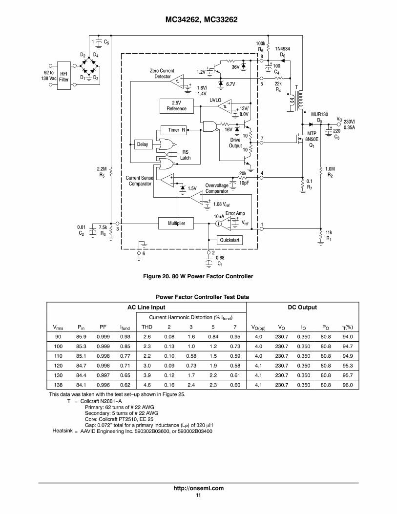
Figure 20. 80 W Power Factor Controller
+
++
RFIFilter
C5
D4
D3
D2
D16.7V
Zero Current Detector
VO
T
UVLO
Current Sense Comparator
RSLatch
1.2V
1.6V/1.4V
36V
2.5VReference
16V10
DriveOutput
10
Timer
Delay
92 to138 Vac
1
22kR4
100kR6 1N4934
D6
1.0MR2
0.1R7
4
7
8
5
6 2
MUR130D5
R
230V/0.35A
0.68C1
1.5V
Error Amp
OvervoltageComparator
+1.08 Vref
+Vref
Quickstart
10�A
10pF
20k
Power Factor Controller Test Data
AC Line Input DC Output
Current Harmonic Distortion (% Ifund)
Vrms Pin PF Ifund THD 2 3 5 7 VO(pp) VO IO PO �(%)
90 85.9 0.999 0.93 2.6 0.08 1.6 0.84 0.95 4.0 230.7 0.350 80.8 94.0
100 85.3 0.999 0.85 2.3 0.13 1.0 1.2 0.73 4.0 230.7 0.350 80.8 94.7
110 85.1 0.998 0.77 2.2 0.10 0.58 1.5 0.59 4.0 230.7 0.350 80.8 94.9
120 84.7 0.998 0.71 3.0 0.09 0.73 1.9 0.58 4.1 230.7 0.350 80.8 95.3
130 84.4 0.997 0.65 3.9 0.12 1.7 2.2 0.61 4.1 230.7 0.350 80.8 95.7
138 84.1 0.996 0.62 4.6 0.16 2.4 2.3 0.60 4.1 230.7 0.350 80.8 96.0
= Coilcraft N2881−APrimary: 62 turns of # 22 AWGSecondary: 5 turns of # 22 AWGCore: Coilcraft PT2510, EE 25Gap: 0.072″ total for a primary inductance (LP) of 320 �H
= AAVID Engineering Inc. 590302B03600, or 593002B03400
T
Heatsink
This data was taken with the test set−up shown in Figure 25.
MC34262, MC33262
http://onsemi.com12
20.68C1
1.5V
Error Amp
OvervoltageComparator
+1.08 Vref
+
Quickstart
10�A
10pF
20k
+
+1.6V/1.4V
Timer R 330C3
100C4
13V/8.0V
MTP14N50E
Q1
1.3MR5
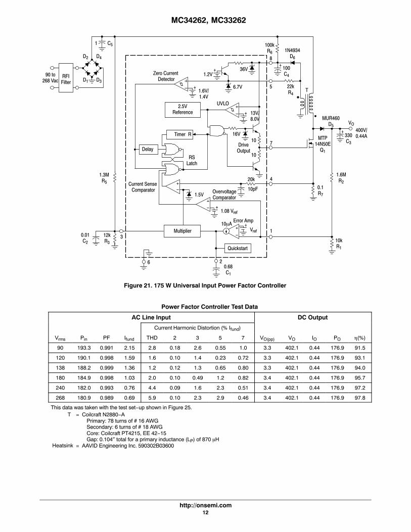
Figure 21. 175 W Universal Input Power Factor Controller
+
++
RFIFilter
C5
D4
D3
D2
D1
0.01C2
6.7V
Zero Current Detector
VO
T
UVLO
Current Sense Comparator
RSLatch
1.2V36V
2.5VReference
16V10
DriveOutput
10
Multiplier
Delay
90 to268 Vac
1
12kR3
22kR4
100kR6 1N4934
D6
10kR1
1.6MR2
0.1R7
4
7
8
5
31
MUR460D5
400V/0.44A
6
Vref
Power Factor Controller Test Data
AC Line Input DC Output
Current Harmonic Distortion (% Ifund)
Vrms Pin PF Ifund THD 2 3 5 7 VO(pp) VO IO PO �(%)
90 193.3 0.991 2.15 2.8 0.18 2.6 0.55 1.0 3.3 402.1 0.44 176.9 91.5
120 190.1 0.998 1.59 1.6 0.10 1.4 0.23 0.72 3.3 402.1 0.44 176.9 93.1
138 188.2 0.999 1.36 1.2 0.12 1.3 0.65 0.80 3.3 402.1 0.44 176.9 94.0
180 184.9 0.998 1.03 2.0 0.10 0.49 1.2 0.82 3.4 402.1 0.44 176.9 95.7
240 182.0 0.993 0.76 4.4 0.09 1.6 2.3 0.51 3.4 402.1 0.44 176.9 97.2
268 180.9 0.989 0.69 5.9 0.10 2.3 2.9 0.46 3.4 402.1 0.44 176.9 97.8
= Coilcraft N2880−APrimary: 78 turns of # 16 AWGSecondary: 6 turns of # 18 AWGCore: Coilcraft PT4215, EE 42−15Gap: 0.104″ total for a primary inductance (LP) of 870 �H
= AAVID Engineering Inc. 590302B03600
T
Heatsink
This data was taken with the test set−up shown in Figure 25.
MC34262, MC33262
http://onsemi.com13
20.68C1
1.5V
Error Amp
OvervoltageComparator
+1.08 Vref
+
Quickstart
10�A
10pF
20k
+
+1.6V/1.4V
Timer R 330C3
100C4
13V/8.0V
MTW20N50E
Q1
1.3MR5
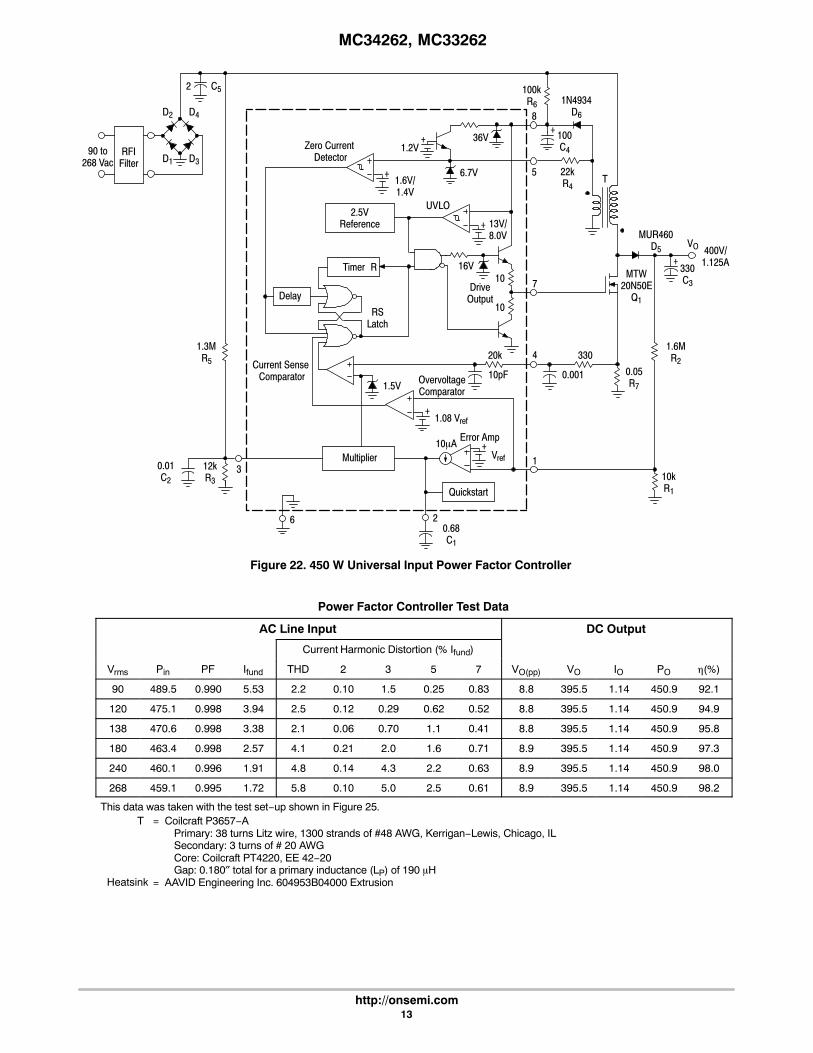
Figure 22. 450 W Universal Input Power Factor Controller
+
++
RFIFilter
C5
D4
D3
D2
D1
0.01C2
6.7V
Zero Current Detector
VO
T
UVLO
Current Sense Comparator
RSLatch
1.2V36V
2.5VReference
16V10
DriveOutput
10
Multiplier
Delay
90 to268 Vac
2
12kR3
22kR4
100kR6 1N4934
D6
10kR1
1.6MR2
0.05R7
4
7
8
5
31
MUR460D5 400V/
1.125A
6
0.001
330
Vref
Power Factor Controller Test Data
AC Line Input DC Output
Current Harmonic Distortion (% Ifund)
Vrms Pin PF Ifund THD 2 3 5 7 VO(pp) VO IO PO �(%)
90 489.5 0.990 5.53 2.2 0.10 1.5 0.25 0.83 8.8 395.5 1.14 450.9 92.1
120 475.1 0.998 3.94 2.5 0.12 0.29 0.62 0.52 8.8 395.5 1.14 450.9 94.9
138 470.6 0.998 3.38 2.1 0.06 0.70 1.1 0.41 8.8 395.5 1.14 450.9 95.8
180 463.4 0.998 2.57 4.1 0.21 2.0 1.6 0.71 8.9 395.5 1.14 450.9 97.3
240 460.1 0.996 1.91 4.8 0.14 4.3 2.2 0.63 8.9 395.5 1.14 450.9 98.0
268 459.1 0.995 1.72 5.8 0.10 5.0 2.5 0.61 8.9 395.5 1.14 450.9 98.2
= Coilcraft P3657−APrimary: 38 turns Litz wire, 1300 strands of #48 AWG, Kerrigan−Lewis, Chicago, ILSecondary: 3 turns of # 20 AWGCore: Coilcraft PT4220, EE 42−20Gap: 0.180″ total for a primary inductance (LP) of 190 �H
= AAVID Engineering Inc. 604953B04000 Extrusion
T
Heatsink
This data was taken with the test set−up shown in Figure 25.
MC34262, MC33262
http://onsemi.com14
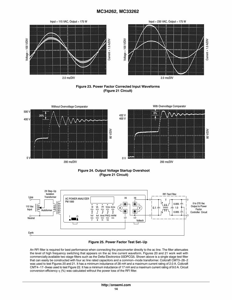
Figure 23. Power Factor Corrected Input Waveforms(Figure 21 Circuit)
Figure 24. Output Voltage Startup Overshoot(Figure 21 Circuit)
Input = 115 VAC, Output = 175 W Input = 230 VAC, Output = 175 W
2.0 ms/DIV 2.0 ms/DIV
Volta
ge =
100
V/D
IV
Cur
rent
= 1
.0 A
/DIV
Volta
ge =
100
V/D
IV
Cur
rent
= 1
.0 A
/DIV
Without Overvoltage Comparator
200 ms/DIV200 ms/DIV
500 V
400 V
0 V
432 V400 V
0 V
80 V
/DIV
80 V
/DIV
26%8%
With Overvoltage Comparator
Figure 25. Power Factor Test Set−Up
0.005
1.00.005
HARMFREQ
11LO
0.1
OI
T0 to 270 Vac
Output to PowerFactor
Controller Circuit
Earth
Line
Neutral
115 VacInput
RFI Test Filter
Autoformer
2X Step-UpIsolation
Transformer
LO
HIHI
VA
AinstAcfVcf
ArmsVrmsPFVAW
1397
53210
Voltech
AC POWER ANALYZERPM 1000
An RFI filter is required for best performance when connecting the preconverter directly to the ac line. The filter attenuatesthe level of high frequency switching that appears on the ac line current waveform. Figures 20 and 21 work well withcommercially available two stage filters such as the Delta Electronics 03DPCG5. Shown above is a single stage test filterthat can easily be constructed with four ac line rated capacitors and a common−mode transformer. Coilcraft CMT3−28−2was used to test Figures 20 and 21. It has a minimum inductance of 28 mH and a maximum current rating of 2.0 A. CoilcraftCMT4−17−9 was used to test Figure 22. It has a minimum inductance of 17 mH and a maximum current rating of 9.0 A. Circuitconversion efficiency � (%) was calculated without the power loss of the RFI filter.
MC34262, MC33262
http://onsemi.com15
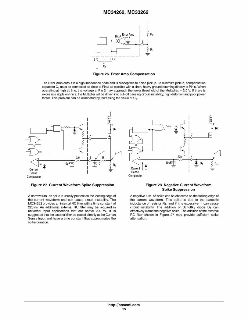
Figure 26. Error Amp Compensation
2
C1
Error Amp+10�A
R1
1
6
R2
The Error Amp output is a high impedance node and is susceptible to noise pickup. To minimize pickup, compensationcapacitor C1 must be connected as close to Pin 2 as possible with a short, heavy ground returning directly to Pin 6. Whenoperating at high ac line, the voltage at Pin 2 may approach the lower threshold of the Multiplier, ≈ 2.0 V. If there isexcessive ripple on Pin 2, the Multiplier will be driven into cut−off causing circuit instability, high distortion and poor powerfactor. This problem can be eliminated by increasing the value of C1.
Figure 27. Current Waveform Spike Suppression
10pF
22k
CurrentSense
Comparator
R7
4
7
C
R
A narrow turn−on spike is usually present on the leading edge ofthe current waveform and can cause circuit instability. TheMC34262 provides an internal RC filter with a time constant of220 ns. An additional external RC filter may be required inuniversal input applications that are above 200 W. It issuggested that the external filter be placed directly at the CurrentSense Input and have a time constant that approximates thespike duration.
Figure 28. Negative Current WaveformSpike Suppression
10pF
22k
CurrentSense
Comparator
R7
4
7
D1
A negative turn−off spike can be observed on the trailing edge ofthe current waveform. This spike is due to the parasiticinductance of resistor R7, and if it is excessive, it can causecircuit instability. The addition of Schottky diode D1 caneffectively clamp the negative spike. The addition of the externalRC filter shown in Figure 27 may provide sufficient spikeattenuation.
MC34262, MC33262
http://onsemi.com16
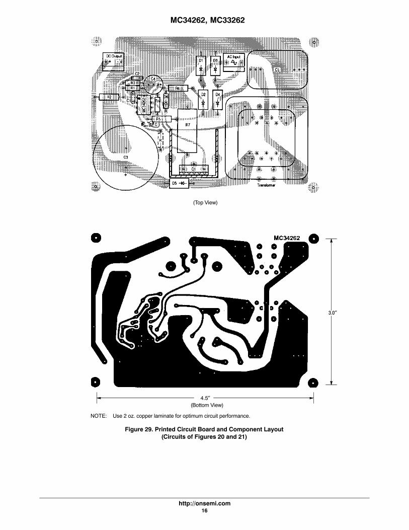
(Top View)
Figure 29. Printed Circuit Board and Component Layout(Circuits of Figures 20 and 21)
4.5″
3.0″
(Bottom View)
NOTE: Use 2 oz. copper laminate for optimum circuit performance.

MC34262, MC33262
http://onsemi.com17
DEVICE ORDERING INFORMATION
Device Operating Temperature Range Package Shipping†
MC34262DG
TA = 0°C to +85°C
SOIC−8(Pb−Free)
98 Units / Rail
MC34262DR2G SOIC−8(Pb−Free)
2500 / Tape & Reel
MC34262PG PDIP−8(Pb−Free)
50 Units / Rail
MC33262DG
TA = −40°C to +105°C
SOIC−8(Pb−Free)
98 Units / Rail
MC33262DR2G SOIC−8(Pb−Free)
2500 / Tape & Reel
MC33262PG PDIP−8(Pb−Free)
50 Units / Rail
MC33262CDR2G SOIC−8(Pb−Free)
2500 / Tape & Reel
†For information on tape and reel specifications, including part orientation and tape sizes, please refer to our Tape and Reel PackagingSpecifications Brochure, BRD8011/D.
MC34262, MC33262
http://onsemi.com18
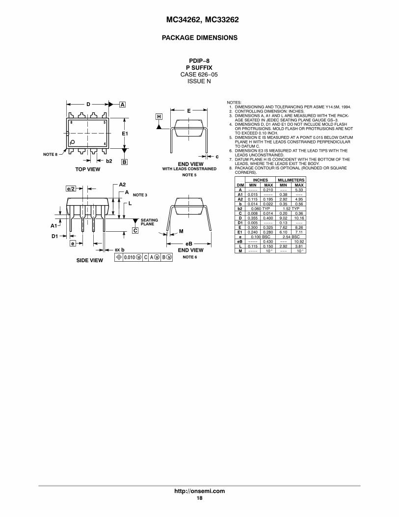
PACKAGE DIMENSIONS
PDIP−8P SUFFIX
CASE 626−05ISSUE N
1 4
58
b2NOTE 8
D
b
L
A1
A
eB
EA
TOP VIEW
C
SEATINGPLANE
0.010 C ASIDE VIEW
END VIEW
END VIEW
WITH LEADS CONSTRAINED
DIM MIN MAXINCHES
A −−−− 0.210A1 0.015 −−−−
b 0.014 0.022
C 0.008 0.014D 0.355 0.400
D1 0.005 −−−−
e 0.100 BSC
E 0.300 0.325
M −−−− 10
−−− 5.330.38 −−−
0.35 0.56
0.20 0.369.02 10.160.13 −−−
2.54 BSC
7.62 8.26
−−− 10
MIN MAXMILLIMETERS
NOTES:1. DIMENSIONING AND TOLERANCING PER ASME Y14.5M, 1994.2. CONTROLLING DIMENSION: INCHES.3. DIMENSIONS A, A1 AND L ARE MEASURED WITH THE PACK-
AGE SEATED IN JEDEC SEATING PLANE GAUGE GS−3.4. DIMENSIONS D, D1 AND E1 DO NOT INCLUDE MOLD FLASH
OR PROTRUSIONS. MOLD FLASH OR PROTRUSIONS ARE NOTTO EXCEED 0.10 INCH.
5. DIMENSION E IS MEASURED AT A POINT 0.015 BELOW DATUMPLANE H WITH THE LEADS CONSTRAINED PERPENDICULARTO DATUM C.
6. DIMENSION E3 IS MEASURED AT THE LEAD TIPS WITH THELEADS UNCONSTRAINED.
7. DATUM PLANE H IS COINCIDENT WITH THE BOTTOM OF THELEADS, WHERE THE LEADS EXIT THE BODY.
8. PACKAGE CONTOUR IS OPTIONAL (ROUNDED OR SQUARECORNERS).
E1 0.240 0.280 6.10 7.11
b2
eB −−−− 0.430 −−− 10.92
0.060 TYP 1.52 TYP
E1
M
8X
c
D1
B
A2 0.115 0.195 2.92 4.95
L 0.115 0.150 2.92 3.81°°
H
NOTE 5
e
e/2A2
NOTE 3
M B M NOTE 6
M

MC34262, MC33262
http://onsemi.com19
PACKAGE DIMENSIONS
SOIC−8D SUFFIX
CASE 751−07ISSUE AK
SEATINGPLANE
14
58
N
J
X 45�
K
NOTES:1. DIMENSIONING AND TOLERANCING PER
ANSI Y14.5M, 1982.2. CONTROLLING DIMENSION: MILLIMETER.3. DIMENSION A AND B DO NOT INCLUDE
MOLD PROTRUSION.4. MAXIMUM MOLD PROTRUSION 0.15 (0.006)
PER SIDE.5. DIMENSION D DOES NOT INCLUDE DAMBAR
PROTRUSION. ALLOWABLE DAMBARPROTRUSION SHALL BE 0.127 (0.005) TOTALIN EXCESS OF THE D DIMENSION ATMAXIMUM MATERIAL CONDITION.
6. 751−01 THRU 751−06 ARE OBSOLETE. NEWSTANDARD IS 751−07.
A
B S
DH
C
0.10 (0.004)
DIMA
MIN MAX MIN MAXINCHES
4.80 5.00 0.189 0.197
MILLIMETERS
B 3.80 4.00 0.150 0.157C 1.35 1.75 0.053 0.069D 0.33 0.51 0.013 0.020G 1.27 BSC 0.050 BSCH 0.10 0.25 0.004 0.010J 0.19 0.25 0.007 0.010K 0.40 1.27 0.016 0.050M 0 8 0 8 N 0.25 0.50 0.010 0.020S 5.80 6.20 0.228 0.244
−X−
−Y−
G
MYM0.25 (0.010)
−Z−
YM0.25 (0.010) Z S X S
M
� � � �
1.520.060
7.00.275
0.60.024
1.2700.050
4.00.155
� mminches
�SCALE 6:1
*For additional information on our Pb−Free strategy and solderingdetails, please download the ON Semiconductor Soldering andMounting Techniques Reference Manual, SOLDERRM/D.
SOLDERING FOOTPRINT*
ON Semiconductor and are registered trademarks of Semiconductor Components Industries, LLC (SCILLC). SCILLC reserves the right to make changes without further noticeto any products herein. SCILLC makes no warranty, representation or guarantee regarding the suitability of its products for any particular purpose, nor does SCILLC assume anyliability arising out of the application or use of any product or circuit, and specifically disclaims any and all liability, including without limitation special, consequential or incidentaldamages. “Typical” parameters which may be provided in SCILLC data sheets and/or specifications can and do vary in different applications and actual performance may vary overtime. All operating parameters, including “Typicals” must be validated for each customer application by customer’s technical experts. SCILLC does not convey any license underits patent rights nor the rights of others. SCILLC products are not designed, intended, or authorized for use as components in systems intended for surgical implant into the body,or other applications intended to support or sustain life, or for any other application in which the failure of the SCILLC product could create a situation where personal injury or deathmay occur. Should Buyer purchase or use SCILLC products for any such unintended or unauthorized application, Buyer shall indemnify and hold SCILLC and its officers, employees,subsidiaries, affiliates, and distributors harmless against all claims, costs, damages, and expenses, and reasonable attorney fees arising out of, directly or indirectly, any claim ofpersonal injury or death associated with such unintended or unauthorized use, even if such claim alleges that SCILLC was negligent regarding the design or manufacture of the part.SCILLC is an Equal Opportunity/Affirmative Action Employer. This literature is subject to all applicable copyright laws and is not for resale in any manner.
MC34262/D
PUBLICATION ORDERING INFORMATIONN. American Technical Support: 800−282−9855 Toll FreeUSA/Canada
Europe, Middle East and Africa Technical Support:Phone: 421 33 790 2910
Japan Customer Focus CenterPhone: 81−3−5817−1050
LITERATURE FULFILLMENT:Literature Distribution Center for ON SemiconductorP.O. Box 5163, Denver, Colorado 80217 USAPhone: 303−675−2175 or 800−344−3860 Toll Free USA/CanadaFax: 303−675−2176 or 800−344−3867 Toll Free USA/CanadaEmail: [email protected]
ON Semiconductor Website: www.onsemi.com
Order Literature: http://www.onsemi.com/orderlit
For additional information, please contact your locaSales Representative