Embed Size (px)
Citation preview

C141-E035-01EN
MAA31xxxx/MAB30xxxx SERIES
DISK DRIVE UNIT
PRODUCT MANUAL
C141-E035-01EN i
REVISION RECORDEdition Date published Revised contents
01 Mar., 1997
Specification No.: C141-E035-**EN
The contents of this manual is subject tochange without prior notice.
All Rights Reserved.Copyright 1996 FUJITSU LIMITED


C141-E035-01EN iii
FOR SAFE OPERATION
Handling of This manual
This manual contains important information for using this product. Read thoroughly beforeusing the product. Use this product only after thoroughly reading and understandingespecially the section “Important Alert Items” in this manual. Keep this manual handy, andkeep it carefully.
FUJITSU makes every effort to prevent users and bystanders from being injured or fromsuffering damange to their property. Use the product according to this manual.
Functional Limitations
There may be certain functional limitations concerning the specifications and functions of theproducts covered by this manual depending on the equipment version, especially concerningthe following functions.
Versions in which there functions can be used will be communicated through“ENGINEERING CHANGE REQUEST/NOTICE”, issued by Fujitsu.
Function Equipment Version Which Supports These Functions
EquipmentVersion No.
EPROMVersion
No.
Standard INQUIRY Data ProductRevision (ASCII)
READ RAM Command
WRITE RAM CommandThese commands cannot be used in the current version.
(Proceed to the Copyright Page)
iv C141-E035-01EN
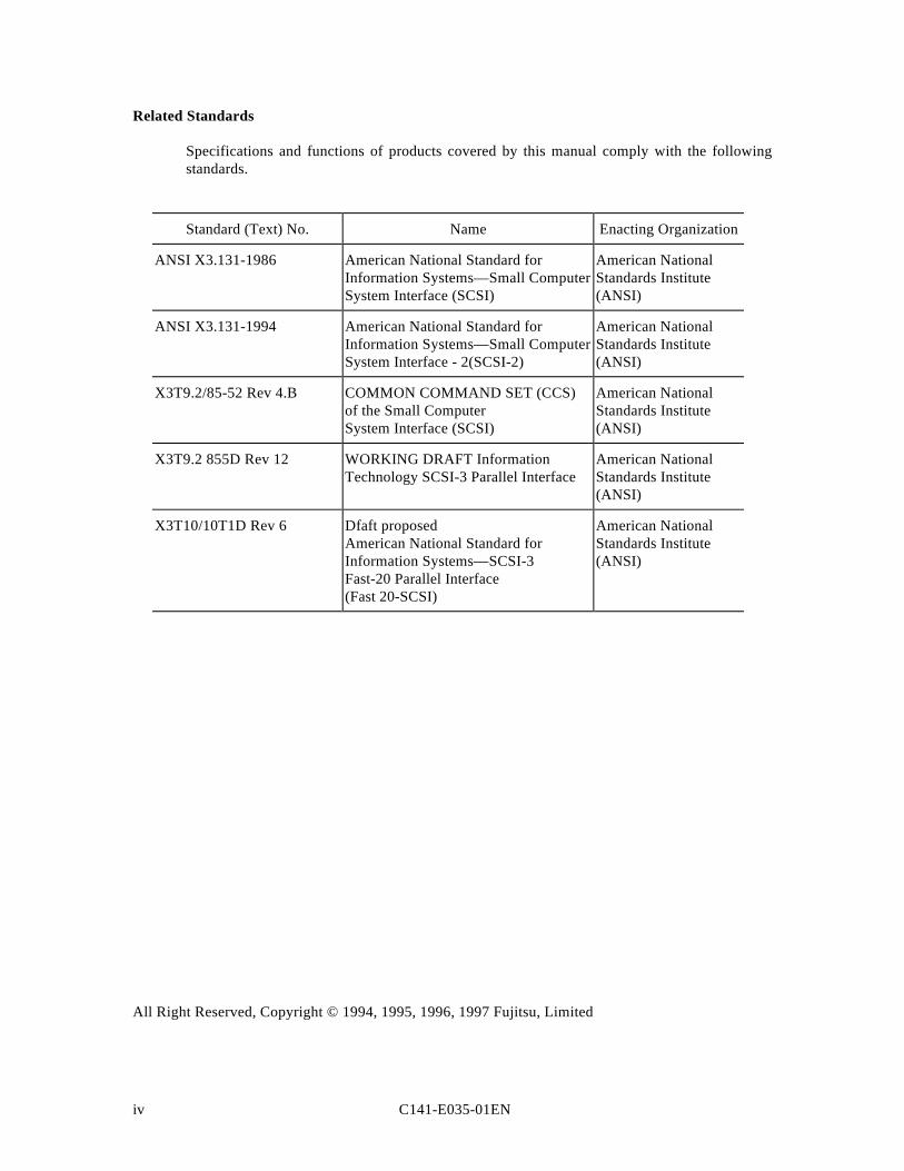
Related Standards
Specifications and functions of products covered by this manual comply with the followingstandards.
Standard (Text) No. Name Enacting Organization
ANSI X3.131-1986 American National Standard forInformation Systems—Small ComputerSystem Interface (SCSI)
American NationalStandards Institute(ANSI)
ANSI X3.131-1994 American National Standard forInformation Systems—Small ComputerSystem Interface - 2(SCSI-2)
American NationalStandards Institute(ANSI)
X3T9.2/85-52 Rev 4.B COMMON COMMAND SET (CCS)of the Small ComputerSystem Interface (SCSI)
American NationalStandards Institute(ANSI)
X3T9.2 855D Rev 12 WORKING DRAFT InformationTechnology SCSI-3 Parallel Interface
American NationalStandards Institute(ANSI)
X3T10/10T1D Rev 6 Dfaft proposedAmerican National Standard forInformation Systems—SCSI-3Fast-20 Parallel Interface(Fast 20-SCSI)
American NationalStandards Institute(ANSI)
All Right Reserved, Copyright © 1994, 1995, 1996, 1997 Fujitsu, Limited
C141-E035-01EN v
PREFACE
This manual describes the MAA3182xx (hereafter, MAA31xxxx), MAB3091xx, MAB3045xx,MAB3024xx (hereafter, MAB30xxxx) series 3.5-inch fixed disk drives with an embedded SCSIcontroller.
This manual details the specifications and functions of the above disk drive, and gives the requirementsand procedures for installing it into a host computer system.
This manual is written for users who have a basic understanding of fixed disk drives and their use incomputer systems. The MANUAL ORGANIZATION section describes organization and scope of thismanual. The need arises, use the other manuals.
Chapter 1 GENERAL DESCRIPTION
This chapter introduces the MAA31xxxx and MAB30xxxx series disk drives and discusses theirstandard features, hardware, and system configuration.
Chapter 2 SPECIFICATIONS
This chapter gives detailed specifications of the MAA31xxxx and MAB30xxxx series disk drives andtheir installation environment.
Chapter 3 DATA FORMAT
This chapter describes the data structure of the disk, the address method, and what to do about mediadefects.
Chapter 4 INSTALLATION REQUIREMENTS
This chapter describes the basic physical and electrical requirements for installing MAA31xxxx andMAB30xxxx series disk drives.
Chapter 5 INSTALLATION
This chapter explains how to install MAA31xxxx and MAB30xxxx series disk drives. It includes thenotice and procedures for setting device number and operation modes, mounting the disk drive,connecting the cables, and confirming drive operation.
Chapter 6 DIAGNOSIS and MAINTENANCE
This chapter describes the automatic diagnosis, and maintenance of the MAA31xxxx and MAB30xxxxseries disk drive.
APPENDIX A to E
The appendixes give supplementary information, including the locations of mounting setting terminalsand connectors, a list of setting items, the signal assignments of interface connectors, lists of modelnames and product numbers, and SCSI interface functions.
The model numbers have a suffix that describes the electrical requirements of the SCSI interfacebetween host system and disk drive, the data formatted at the factory and device type.
vi C141-E035-01EN
CONVENTIONS
This manual uses the following conventions for alerts to prevent physical or property damages to usersor by standards.
DANGER
DANGER indicates that personal injury will occur if the user does not perform the procedurecorrectly.
WARNING
WARNING indicates that personal injury could occur if the user does not perform the procedurecorrectly.
CAUTION
CAUTION indicates that either minor or moderate personal injury may occur if the user does notperform the procedure correctly.
NOTICE
NOTICE indicates that inconvenience to the user such as damages to the product, equipment, data,and/or other property may occur if the user does not pay attention or perform the procedure correctly.
IMPORTANT
IMPORTANT indicates information that the helps the user use the product more effectively.
Indicates
This manual indicates;
Decimal number: Indicates as it is.
Hexadecimal number: Indicates as X’17B9’, 17B9h, or 17B9H
Binary number: Indicates as “010”
C141-E035-01EN vii
DISCLAIMER
Failure of the M2949, M2952, and M2954 series intelligent disk drive is defined as a failure requiringadjustments, repairs, or replacement. Fujitsu is not responsible for drive failures caused by misuse bythe user, poor environmental conditions, power trouble, host problems, cable failures, or any failure notcaused by the drive itself.
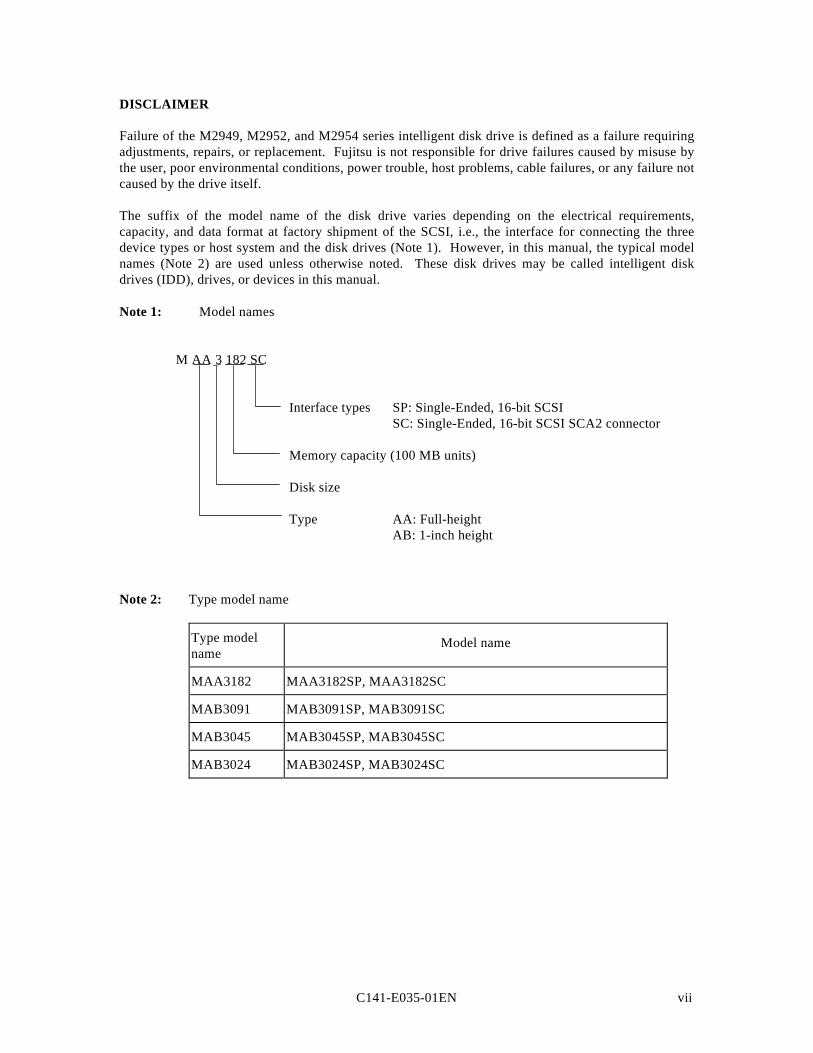
The suffix of the model name of the disk drive varies depending on the electrical requirements,capacity, and data format at factory shipment of the SCSI, i.e., the interface for connecting the threedevice types or host system and the disk drives (Note 1). However, in this manual, the typical modelnames (Note 2) are used unless otherwise noted. These disk drives may be called intelligent diskdrives (IDD), drives, or devices in this manual.
Note 1: Model names
M AA 3 182 SC
Interface types SP: Single-Ended, 16-bit SCSISC: Single-Ended, 16-bit SCSI SCA2 connector
Memory capacity (100 MB units)
Disk size
Type AA: Full-heightAB: 1-inch height
Note 2: Type model name
Type modelname
Model name
MAA3182 MAA3182SP, MAA3182SC
MAB3091 MAB3091SP, MAB3091SC
MAB3045 MAB3045SP, MAB3045SC
MAB3024 MAB3024SP, MAB3024SC
viii C141-E035-01EN
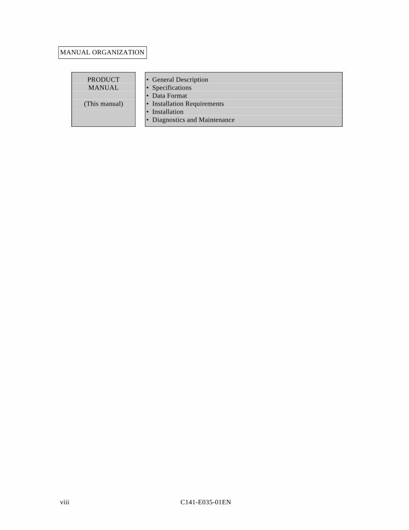
MANUAL ORGANIZATION
PRODUCTMANUAL
(This manual)
• General Description• Specifications• Data Format• Installation Requirements• Installation• Diagnostics and Maintenance
C141-E035-01EN ix
CONTENTS
pageCHAPTER 1 GENERAL DESCRIPTION .......................................................................... 1-1
1.1 Standard Features ........................................................................................................... 1-2
1.2 Hardware Structure......................................................................................................... 1-5
1.3 System Configuration..................................................................................................... 1-8
CHAPTER 2 SPECIFICATIONS......................................................................................... 2-1
2.1 Hardware Specifications ................................................................................................. 2-1
2.1.1 Model name and part number......................................................................................... 2-1
2.1.2 Function specifications................................................................................................... 2-2
2.1.3 Environmental specifications.......................................................................................... 2-4
2.1.4 Error rate......................................................................................................................... 2-5
2.1.5 Reliability ....................................................................................................................... 2-5
2.2 SCSI Function Specifications ......................................................................................... 2-7
CHAPTER 3 DATA FORMAT ............................................................................................ 3-1
3.1 Data Space...................................................................................................................... 3-1
3.1.1 Cylinder configuration.................................................................................................... 3-1
3.1.2 Alternate spare area ........................................................................................................ 3-5
3.1.3 Track format ................................................................................................................... 3-6
3.1.4 Sector format .................................................................................................................. 3-8
3.1.5 Format capacity .............................................................................................................. 3-10
3.2 Logical Data Block Addressing...................................................................................... 3-11
3.3 Defect Management........................................................................................................ 3-12
3.3.1 Defect list ....................................................................................................................... 3-12
3.3.2 Alternate block allocation............................................................................................... 3-12
CHAPTER 4 INSTALLATION REQUIREMENTS .......................................................... 4-1
4.1 Mounting Requirements ................................................................................................. 4-1
4.1.1 External dimensions ....................................................................................................... 4-1
4.1.2 Mounting........................................................................................................................ 4-4
4.1.3 Notes on mounting ......................................................................................................... 4-4
4.2 Power Supply Requirements .......................................................................................... 4-9
x C141-E035-01EN
4.3 Connection Requirements .............................................................................................. 4-12
4.3.1 16-bit SCSI model (MAA31xxSP, MAB30xxSP).......................................................... 4-12
4.3.2 SCA type SCSI model (MAA31xxSC, MAB30xxSC)................................................... 4-20
4.3.3 Cable connector requirements ........................................................................................ 4-22
4.3.4 External operator panel................................................................................................... 4-28
CHAPTER 5 INSTALLATION............................................................................................ 5-1
5.1 Notes on Handling Drives .............................................................................................. 5-1
5.2 Connections.................................................................................................................... 5-3
5.3 Setting Terminals............................................................................................................ 5-5
5.3.1 SCSI ID setting............................................................................................................... 5-7
5.3.2 Each mode setting .......................................................................................................... 5-8
5.3.3 Write protect, terminating resistor setting....................................................................... 5-9
5.3.4 Mode settings ................................................................................................................. 5-10
5.4 Mounting Drives ............................................................................................................ 5-11
5.4.1 Check before mounting .................................................................................................. 5-11
5.4.2 Mounting procedures...................................................................................................... 5-11
5.5 Connecting Cables.......................................................................................................... 5-13
5.6 Confirming Operations after Installation and Preparation for use .................................. 5-14
5.6.1 Confirming initial operations.......................................................................................... 5-14
5.6.2 Checking SCSI connection............................................................................................. 5-16
5.6.3 Formatting ...................................................................................................................... 5-19
5.6.4 Setting parameters .......................................................................................................... 5-21
5.7 Dismounting Drives ....................................................................................................... 5-25
CHAPTER 6 DIAGNOSTICS AND MAINTENANCE...................................................... 6-1
6.1 Diagnostics ..................................................................................................................... 6-1
6.1.1 Self-diagnostics .............................................................................................................. 6-1
6.1.2 Test programs ................................................................................................................. 6-5
6.2 Maintenance Information ............................................................................................... 6-6
6.2.1 Maintenance requirements.............................................................................................. 6-6
6.2.2 Revision numbers........................................................................................................... 6-8
APPENDIX A LOCATIONS OF CONNECTORS, SETTING TERMINALS, AND
TERMINATING RESISTORS...................................................................... A-1
C141-E035-01EN xi
A.1 Locations of Connectors and Setting Terminals
(MAx3xxSC, SCA type 16-bit SCSI)............................................................................. A-2
A.2 Locations of Connectors and Setting Terminals
(MAx3xxSP, single-ended type 16-bit SCSI)................................................................. A-3
APPENDIX B SETTING TERMINALS................................................................................ B-1
B.1 Setting Terminals (MAx3xxxSS : Single-ended 8-bit SCSI).......................................... B-2
APPENDIX C CONNECTOR SIGNAL ALLOCATION .................................................... C-1
C.1 SCSI Connector Signal Allocation: single-ended 8-bit SCSI ........................................ C-2
C.2 SCSI Connector Signal Allocation: SCA type 16-bit SCSI........................................... C-3
APPENDIX D MODEL NAMES AND PRODUCT NUMBERS ......................................... D-1
D.1 Model Names and Product Numbers.............................................................................. D-2
APPENDIX E SCSI INTERFACE FUNCTIONS ................................................................. E-1
xii C141-E035-01EN
FIGURES
page1.1 MAA31xxxx outer view................................................................................................. 1-5
1.2 MAB30xxxx outer view................................................................................................. 1-6
1.3 Disk/head configuration ................................................................................................. 1-7
1.4 System configuration...................................................................................................... 1-8
3.1 Cylinder configuration.................................................................................................... 3-2
3.2 Spare area in cylinders.................................................................................................... 3-5
3.3 Alternate cylinder ........................................................................................................... 3-5
3.4 Track format ................................................................................................................... 3-6
3.5 Track skew/cylinder skew .............................................................................................. 3-7
3.6 Sector format .................................................................................................................. 3-8
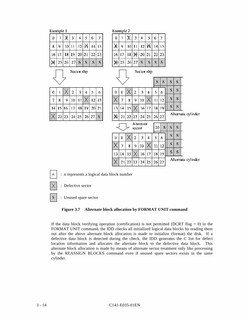
3.7 Alternate block allocation by FORMAT UNIT command ............................................. 3-14
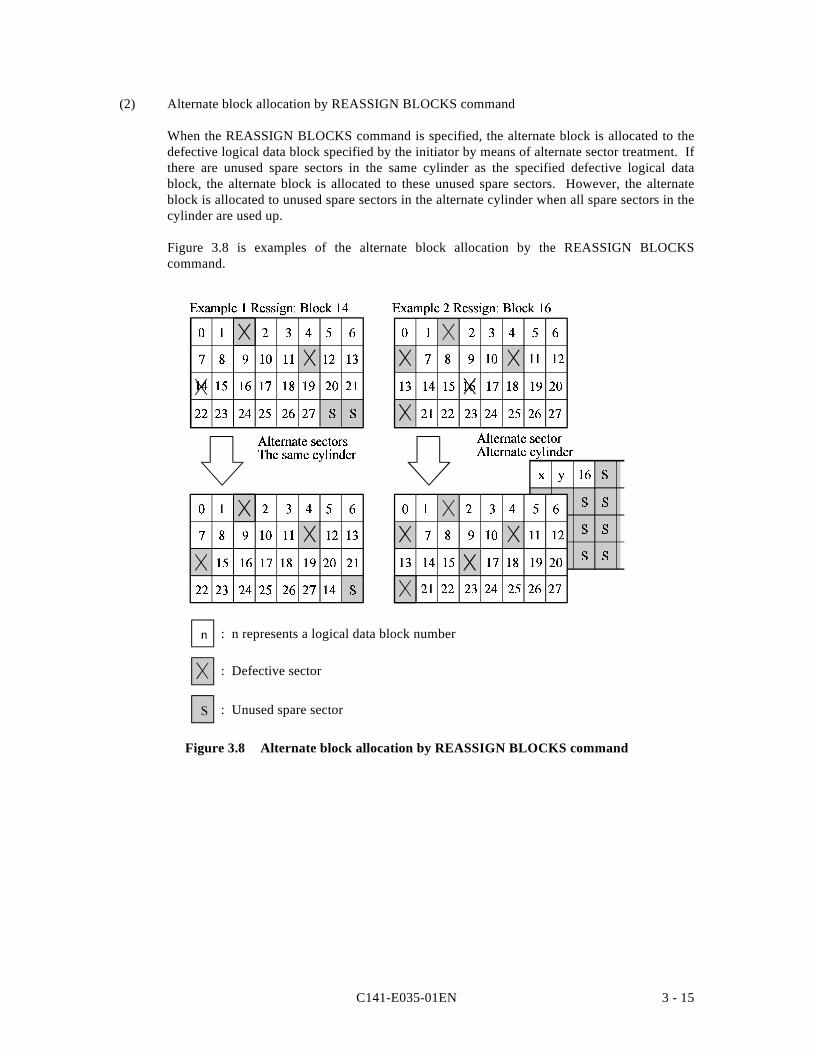
3.8 Alternate block allocation by REASSIGN BLOCKS command..................................... 3-15
4.1 External dimensions (MAA3xxx)................................................................................... 4-2
4.2 External dimensions (MAB3xxx)................................................................................... 4-3
4.3 IDD orientation............................................................................................................... 4-4
4.4 Mounting frame structure ............................................................................................... 4-5
4.5 Limitation of side-mounting........................................................................................... 4-5
4.6 Surface temperature measurement points (MAA3)......................................................... 4-7
4.7 Service clearance area (MAA3) ...................................................................................... 4-7
4.8 Air pressure adjustment hole .......................................................................................... 4-8
4.9 Current waveform (+12 VDC)........................................................................................ 4-9
4.10 Power on/off sequence (1) .............................................................................................. 4-9
4.11 Power on/off sequence (2) .............................................................................................. 4-10
4.12 Power on/off sequence (3) .............................................................................................. 4-10
4.13 AC noise filter (recommended) ...................................................................................... 4-11
4.14 Connectors and terminals location (single-ended 16-bit SCSI) ...................................... 4-12
4.15 16-bit SCSI interface connector...................................................................................... 4-13
4.16 Power supply connector (16-bit SCSI model) ................................................................ 4-13
4.17 External operator panel (2) (16-bit SCSI model) ............................................................ 4-14
4.18 External operator panel connector (M295xQ/R)............................................................. 4-15
4.19 16-bit SCSI ID external input ......................................................................................... 4-16
4.20 Output signal for external LED ...................................................................................... 4-17
C141-E035-01EN xiii
4.21 Cables connection (16-bit SCSI model) ......................................................................... 4-19
4.22 Connectors and terminals location of SCA2 type SCSI model....................................... 4-20
4.23 SCA type SCSI connector .............................................................................................. 4-21
4.24 SCSI cable connector (1 of 2)......................................................................................... 4-23
4.24 SCSI cable connector (2 of 2)......................................................................................... 4-24
4.25 SCSI cable termination................................................................................................... 4-26
4.26 External operator panel circuit example (MAA3xxxSP, MAB3xxxSD) ........................ 4-28
5.1 SCSI bus connections (1 of 2) ........................................................................................ 5-3
5.1 SCSI bus connections (2 of 2) ........................................................................................ 5-4
5.2 MAx3xxxSC setting terminals position ......................................................................... 5-5
5.3 Setting terminals (MAx3xxxSP)..................................................................................... 5-6
5.4 Checking the SCSI connection (A)................................................................................. 5-17
5.5 Checking the SCSI connection (B)................................................................................. 5-18
6.1 Revision label ................................................................................................................. 6-8
6.2 Indicating revision numbers ........................................................................................... 6-9
A.1 Locations of connectors and setting terminals
(MAx3xxSC, SCA type 16-bit SCSI)................................................................................ A-6
A.2 Locations of connectors and setting terminals
(MAx3xxSP, single-ended type 16-bit SCSI) .................................................................... A-7
xiv C141-E035-01EN
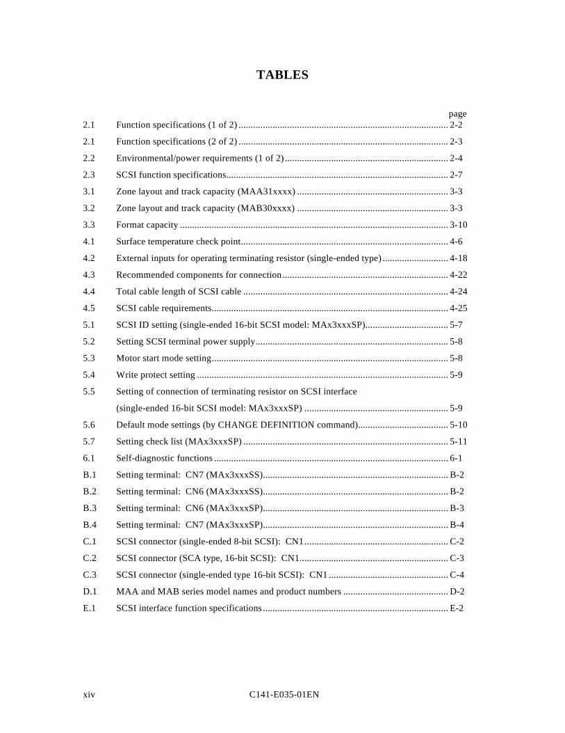
TABLES
page2.1 Function specifications (1 of 2) ...................................................................................... 2-2
2.1 Function specifications (2 of 2) ...................................................................................... 2-3
2.2 Environmental/power requirements (1 of 2) ................................................................... 2-4
2.3 SCSI function specifications........................................................................................... 2-7
3.1 Zone layout and track capacity (MAA31xxxx) .............................................................. 3-3
3.2 Zone layout and track capacity (MAB30xxxx) .............................................................. 3-3
3.3 Format capacity .............................................................................................................. 3-10
4.1 Surface temperature check point..................................................................................... 4-6
4.2 External inputs for operating terminating resistor (single-ended type) ........................... 4-18
4.3 Recommended components for connection.................................................................... 4-22
4.4 Total cable length of SCSI cable .................................................................................... 4-24
4.5 SCSI cable requirements................................................................................................. 4-25
5.1 SCSI ID setting (single-ended 16-bit SCSI model: MAx3xxxSP).................................. 5-7
5.2 Setting SCSI terminal power supply............................................................................... 5-8
5.3 Motor start mode setting................................................................................................. 5-8
5.4 Write protect setting ....................................................................................................... 5-9
5.5 Setting of connection of terminating resistor on SCSI interface
(single-ended 16-bit SCSI model: MAx3xxxSP) ........................................................... 5-9
5.6 Default mode settings (by CHANGE DEFINITION command)..................................... 5-10
5.7 Setting check list (MAx3xxxSP) .................................................................................... 5-11
6.1 Self-diagnostic functions ................................................................................................ 6-1
B.1 Setting terminal: CN7 (MAx3xxxSS)............................................................................ B-2
B.2 Setting terminal: CN6 (MAx3xxxSS)............................................................................ B-2
B.3 Setting terminal: CN6 (MAx3xxxSP)............................................................................ B-3
B.4 Setting terminal: CN7 (MAx3xxxSP)............................................................................ B-4
C.1 SCSI connector (single-ended 8-bit SCSI): CN1........................................................... C-2
C.2 SCSI connector (SCA type, 16-bit SCSI): CN1............................................................. C-3
C.3 SCSI connector (single-ended type 16-bit SCSI): CN1 ................................................. C-4
D.1 MAA and MAB series model names and product numbers ........................................... D-2
E.1 SCSI interface function specifications............................................................................ E-2
C141-E035-01EN 1 - 1
CHAPTER 1 GENERAL DESCRIPTION
1.1 Standard Features
1.2 Hardware Structure
1.3 System Configuration
This chapter describes the feature and configuration of the intelligent disk drives (IDD).
IDDs are high performance large capacity 3.5-inch fixed disk drives with an embedded SCSIcontroller.
The interface between the IDD and host system is based on SCSI (Small Computer System Interface)standard [ANSI X3.131 - 1986: Small Computer System Interface (SCSI), ANSI X3.131-1994: SmallComputer System Interface - 2 (SCSI-2)].
The flexibility and expandability of the SCSI, as well as the powerful command set of the IDD, allowthe user to construct a high-performance reliable disk subsystem with large storage capacity.
C141-E035-01EN1 - 2
1.1 Standard Features
(1) Compactness
Since the SCSI controller circuit is embedded in the standard 3.5-inch fixed disk drive formfactor, the IDD is extremely compact. The IDD can be connected directly to the SCSI bus ofthe host system .
(2) SCSI/CCS standard
The IDD provides not only SCSI basic functions but also the following features:
• Arbitration• Disconnection/reselection• Data bus parity• Command set which meets the logical specification of the SCSI CCS (Common
Command Set for Direct Access Device) requirements (Rev. 4.B)
The SCSI commands can manipulate data through logical block addressing regardless of thephysical characteristics of the disk drive. This allows software to accommodate futureexpansion of system functions.
(3) 8-bit SCSI/16-bit SCSI
The following IDDs are available. MAx3xxxSP/SC with 16-bit data width (16-bit SCSI),which have the wide transfer function suitable for SCSI-3.
• 8-bit SCSI: Up to eight SCSI devices can be connected on the same SCSI bus.• 16-bit SCSI: Up to 16 SCSI devices can be connected on the same SCSI bus.
For the ultra SCSI model, number of connectable SCSI devices on the same SCSI bus is variedas follows.
• Up to 4 SCSI devices having capacitance of 25 pF: Cable length of up to 3.0 m.• 5 to 8 SCSI devices having capacitance of 25 pF: Cable length of up to 1.5 m
(4) High speed data transfer
• 8-bit SCSI: The data transfer rate on the 8-bit SCSI bus is 6 MB/s maximum inasynchronous mode, 20 MB/s in synchronous mode.
• 16-bit SCSI: The data transfer rate on the 16-bit SCSI bus is 12 MB/s maximum inasynchronous mode, 40 MB/s in synchronous mode.
Such a high data transfer rate on the SCSI bus can be useful with the large capacity buffer inthe IDD.
C141-E035-01EN 1 - 3
Note:
The maximum data transfer rate in asynchronous mode may be limited by the responsetime of initiator and the length of SCSI bus length. The maximum data transfer rate insynchronous mode on the single-ended SCSI bus may be limited by the cable length,transmission characteristics of the SCSI bus and the connected SCSI device number.
(5) Continuous block processing
The addressing method of data blocks is logical block address. The initiator can access databy specifying block number in a logically continuous data space without concerning thephysical structure of the track or cylinder boundaries.
The continuous processing up to [64K-1] blocks in a command can be achieved, and IDD canperform continuous read/write operation when processing data blocks on several tracks orcylinder.
(6) 512 KB programmable multi-segment data buffer
Data is transferred between SCSI bus and disk media through the embedded 512 KB databuffer in the IDD. This buffer can be divided into maximum 32 areas. This feature providesthe suitable usage environment for users.
Since the initiator can control the disconnect/reconnect timing on the SCSI bus by specifyingthe condition of stored data to the data buffer or empty condition of the data buffer, theinitiator can perform the effective input/output operations with utilizing high data transfercapability of the SCSI bus regardless of actual data transfer rate of the disk drive.
(7) Read-ahead cache feature
After executing the READ command, the IDD reads automatically and stores (prefetches) thesubsequent data blocks into the data buffer (Read-ahead caching).
The high speed sequential data access can be achieved by transferring the data from the databuffer without reaccessing the disk in case the subsequent command requests the prefetcheddata blocks.
(8) Command queuing feature
The IDD can queue maximum 128 commands, and optimizes the issuing order of queuedcommands by the reordering function. This feature realizes the high speed processing.
(9) Reserve and release functions
The IDD can be accessed exclusively in the multi-host or multi-initiator environment by usingthe reserve and release functions.
C141-E035-01EN1 - 4
(10) Error recovery
The IDD can try to recover from errors in SCSI bus or the disk drive using its powerful retryprocessing. If a recoverable data check occurs, error-free data can be transferred to theinitiator after being corrected in the data buffer. The initiator software is released from thecomplicated error recover processing by these error recovery functions of the IDD.
(11) Automatic alternate block reassignment
If a defective data block is detected during read, the IDD can automatically reassign itsalternate data block.
(12) Programmable data block length
Data can be accessed in fixed-block length units. The data block length is programmable, andcan at initializing with a multiple of two for the 512 to 528 bytes.
(13) Defective block slipping
A logical data block can be reallocated in a physical sequence by slipping the defective datablock at formatting. This results in high speed contiguous data block processing without arevolution delay due to defective data block.
(14) High speed positioning
A rotary voice coil motor achieves fast positioning.
(15) Large capacity
A large capacity can be obtained from 3.5-inch disk drives by dividing all cylinders intoseveral partitions and changing the recording density on each partition (constant densityrecording). The disk subsystem with large capacity can be constructed in the good spaceefficiency.
(16) Start/Stop of spindle motor
Using the SCSI command, the host system can start and stop the spindle motor.
(17) Diagnosis
The IDD has a diagnostic capability which checks internal controller functions and driveoperations to facilitate testing and repair.
C141-E035-01EN 1 - 5
(18) Low power consumption
By using highly integrated LSI components, the power consumption of the IDD is very low,and this enables the unit to be used in wide range of environmental conditions.
(19) Low noise and low vibration
Approx. 4.3 bels for MAA31xxxx and 4.2 bels for MAB30xxxx. This makes it ideal foroffice use. The IDD has rubber vibration isolators, which minimize the transfer of vibration.
(20) Microcode downloading
The IDD implements the microcode download feature. This feature achieves easymaintainability of the IDD and function enhancing.
1.2 Hardware Structure
An outer view of the IDD is given in Figure 1.1. The IDD is composed of the disk, head,spindle motor, hermetically sealed disk enclosure (DE) with actuator and air circulation filter,as well as read/write pre-amp with the print card unit (PCA) of the controller.
Figure 1.1 MAA31xxxx outer view
C141-E035-01EN1 - 6
Figure 1.2 MAB30xxxx outer view
(1) Disks
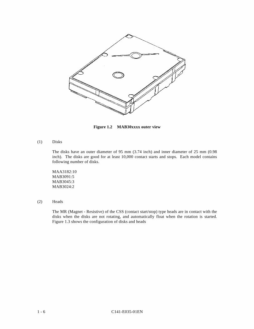
The disks have an outer diameter of 95 mm (3.74 inch) and inner diameter of 25 mm (0.98inch). The disks are good for at least 10,000 contact starts and stops. Each model containsfollowing number of disks.
MAA3182:10MAB3091:5MAB3045:3MAB3024:2
(2) Heads
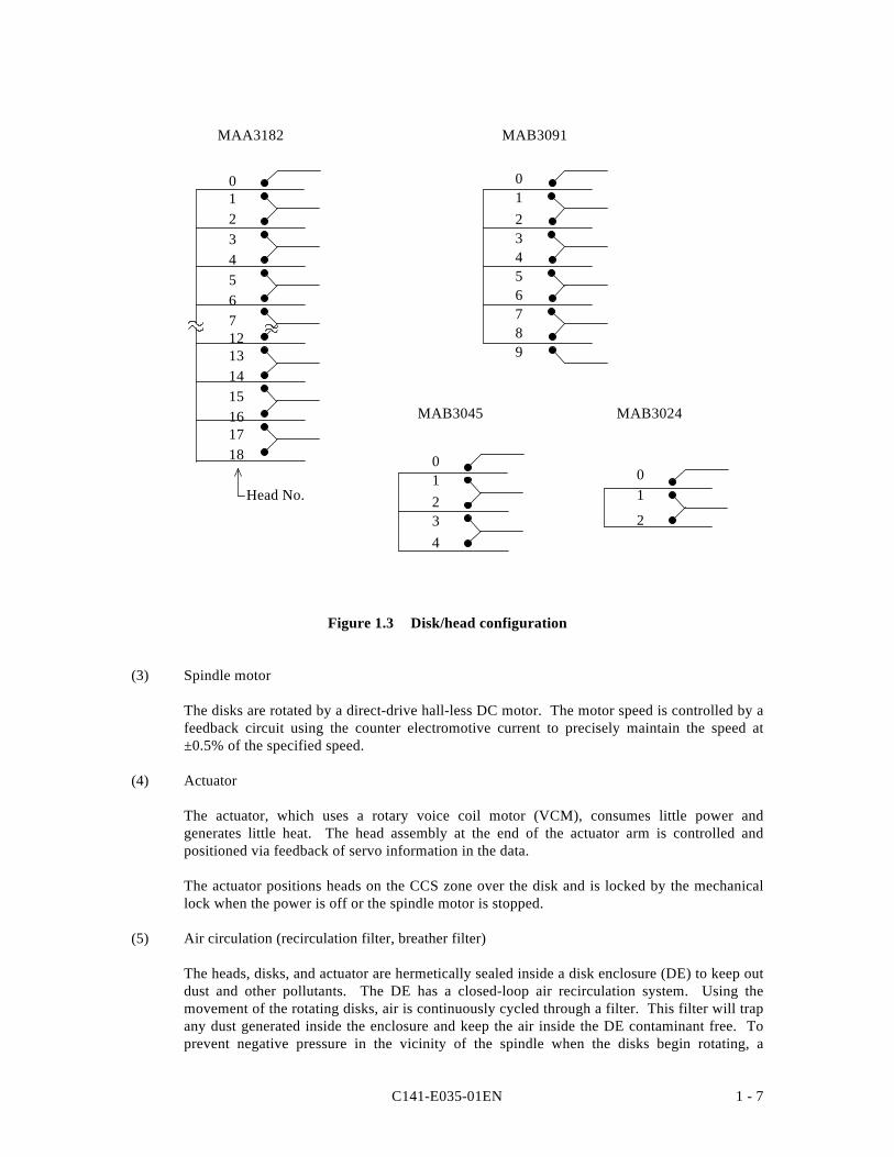
The MR (Magnet - Resistive) of the CSS (contact start/stop) type heads are in contact with thedisks when the disks are not rotating, and automatically float when the rotation is started.Figure 1.3 shows the configuration of disks and heads
C141-E035-01EN 1 - 7
Figure 1.3 Disk/head configuration
(3) Spindle motor
The disks are rotated by a direct-drive hall-less DC motor. The motor speed is controlled by afeedback circuit using the counter electromotive current to precisely maintain the speed at±0.5% of the specified speed.
(4) Actuator
The actuator, which uses a rotary voice coil motor (VCM), consumes little power andgenerates little heat. The head assembly at the end of the actuator arm is controlled andpositioned via feedback of servo information in the data.
The actuator positions heads on the CCS zone over the disk and is locked by the mechanicallock when the power is off or the spindle motor is stopped.
(5) Air circulation (recirculation filter, breather filter)
The heads, disks, and actuator are hermetically sealed inside a disk enclosure (DE) to keep outdust and other pollutants. The DE has a closed-loop air recirculation system. Using themovement of the rotating disks, air is continuously cycled through a filter. This filter will trapany dust generated inside the enclosure and keep the air inside the DE contaminant free. Toprevent negative pressure in the vicinity of the spindle when the disks begin rotating, a
MAB3091
0123456789
0123456712131415161718
MAA3182
Head No.
01234
MAB3045
01
2
MAB3024
C141-E035-01EN1 - 8
breather filter is attached. The breather filter also equalizes the internal air pressure with theatmospheric pressure due to surrounding temperature changes.
(6) Read/write circuit
The read/write circuit uses head LSI chips and partial response class 4 maximum likelihood(PR4ML) modulator and demodulator circuit to prevent errors caused by external noise, thusimproving data reliability.
(7) Controller circuit
The controller circuit uses LSIs to increase the reliability and uses a high speedmicroprocessing unit (MPU) to increase the performance of the SCSI controller.
1.3 System Configuration
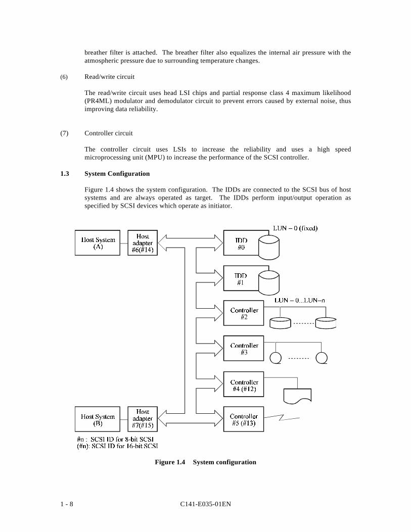
Figure 1.4 shows the system configuration. The IDDs are connected to the SCSI bus of hostsystems and are always operated as target. The IDDs perform input/output operation asspecified by SCSI devices which operate as initiator.
Figure 1.4 System configuration
C141-E035-01EN 1 - 9
(1) SCSI bus configuration
Up to eight SCSI devices operating as an initiator or a target can be connected to the SCSI busfor the 8-bit SCSI and up to 16 SCSI devices operating as an initiator or a target can beconnected to the SCSI bus for the 16-bit SCSI in any combination.
For example, the system can be configured as multi-host system on which multiple hostcomputers that operate as initiator or connected through the SCSI bus.
Using disconnect/reconnect function, concurrent input/output processing is possible on multi-SCSI devices.
(2) Addressing of peripheral device
Each SCSI device on the bus has its own unique address (SCSI ID:#n in Figure 1.4). Forinput/output operation, a peripheral device attached to the SCSI bus that operates as target isaddressed in unit called as logical unit. A unique address (LUN: logical unit number) isassigned for each logical unit.
The initiator selects one SCSI device by specifying that SCSI ID, then specifies the LUN toselect the peripheral device for input/output operation.
The IDD is constructed so that the whole volume of disk drive is a single logical unit, theselectable number of SCSI ID and LUN are as follows:
• SCSI ID: 8-bit SCSI:Selectable from 0 to 7 (switch selectable)16-bit SCSI:Selectable from 0 to 15 (switch selectable)
• LUN: 0 (fixed)

C141-E035-01EN 2 - 1
CHAPTER 2 SPECIFICATIONS
2.1 Hardware Specifications
2.2 SCSI Function Specifications
This chapter describes specifications of the IDD and the functional specifications of the SCSI.
2.1 Hardware Specifications
2.1.1 Model name and part number
Each model has a different data format, front panel, and mounting screw type when shipped.(See Appendix D for the model name (type) and product number.)
The data format can be changed by reinitializing with the user's system.
C141-E035-01EN2 - 2
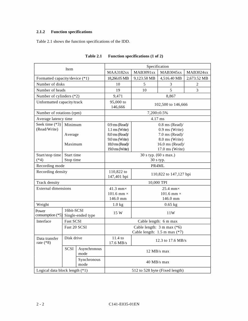
2.1.2 Function specifications
Table 2.1 shows the function specifications of the IDD.
Table 2.1 Function specifications (1 of 2)
SpecificationMAA3182xx MAB3091xx MAB3045xx MAB3024xx
Formatted capacity/device (*1) 18,266.05 MB 9,123.58 MB 4,516.40 MB 2,673.52 MBNumber of disks 10 5 3 2Number of heads 19 10 5 3Number of cylinders (*2) 9,471 8,867Unformatted capacity/track 95,000 to
146,666 102,500 to 146,666
Number of rotations (rpm) 7,200±0.5%Average latency time 4.17 ms
Minimum
Average
Maximum
0.9 ms (Read)/1.1 ms (Write)8.0 ms (Read)/9.0 ms (Write)18.0 ms (Read)/19.0 ms (Write)
0.8 ms (Read)/0.9 ms (Write)7.0 ms (Read)/8.0 ms (Write)
16.0 ms (Read)/17.0 ms (Write)
Start timeStop time
30 s typ. (60 s max.)30 s typ.
Recording mode PR4MLRecording density 110,822 to
147,401 bpi 110,822 to 147,127 bpi
Track density 10,000 TPIExternal dimensions 41.3 mm×
101.6 mm ×146.0 mm
25.4 mm×101.6 mm ×146.0 mm
Weight 1.0 kg 0.65 kg16bit-SCSISingle-ended type 15 W 11W
Interface Fast SCSI Cable length: 6 m maxFast 20 SCSI Cable length: 3 m max (*6)
Cable length: 1.5 m max (*7)Disk drive 11.4 to
17.6 MB/s 12.3 to 17.6 MB/s
SCSI Asynchronousmode 12 MB/s max
Synchronousmode 40 MB/s max
Logical data block length (*1) 512 to 528 byte (Fixed length)
Data transferrate (*8)
Powerconsumption (*5)
Start/stop time(*4)
Seek time (*3)(Read/Write)
Item
C141-E035-01EN 2 - 3
Table 2.1 Function specifications (2 of 2)
Item Specification
SCSI command specification
ANSI X3.13-1986 and CCS (Rev. 4B) conformitySCSI-2 (ANSI X3T9.2/86-109 Rev 10h) command supportSCSI-3 command partial supportFujitsu-specific command
Data buffer 512 KB FIFO ring buffer, multi-segment buffer: Segmentcount 1 to 32, Read-ahead cache
(*1) The formatted capacity can be changed by changing the logical block length and using sparesector space. See Chapter 3 for the further information.
(*2) The number of user cylinders indicates the max., and includes the alternate cylinder. Thenumber of user cylinders and alternate cylinders can be specified at format of the IDD.
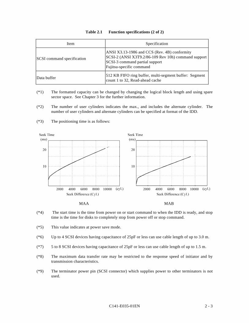
(*3) The positioning time is as follows:
(*4) The start time is the time from power on or start command to when the IDD is ready, and stoptime is the time for disks to completely stop from power off or stop command.
(*5) This value indicates at power save mode.
(*6) Up to 4 SCSI devices having capacitance of 25pF or less can use cable length of up to 3.0 m.
(*7) 5 to 8 SCSI devices having capacitance of 25pF or less can use cable length of up to 1.5 m.
(*8) The maximum data transfer rate may be restricted to the response speed of initiator and bytransmission characteristics.
(*9) The terminator power pin (SCSI connector) which supplies power to other terminators is notused.
6 100008000600040002000
MAA MAB
100008000600040002000
C141-E035-01EN2 - 4
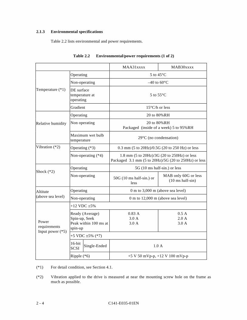
2.1.3 Environmental specifications
Table 2.2 lists environmental and power requirements.
Table 2.2 Environmental/power requirements (1 of 2)
MAA31xxxx MAB30xxxx
Operating 5 to 45°C
Non-operating –40 to 60°C
DE surfacetemperature atoperating
5 to 55°C
Gradient 15°C/h or less
Operating 20 to 80%RH
Non operating 20 to 80%RHPackaged (inside of a week) 5 to 95%RH
Maximum wet bulbtemperature 29°C (no condensation)
Operating (*3) 0.3 mm (5 to 20Hz)/0.5G (20 to 250 Hz) or less
Non-operating (*4) 1.8 mm (5 to 20Hz)/3G (20 to 250Hz) or lessPackaged 3.1 mm (5 to 20Hz)/5G (20 to 250Hz) or less
Operating 5G (10 ms half-sin.) or less
Non-operating 50G (10 ms half-sin.) orless
MAB only 60G or less(10 ms half-sin)
Operating 0 m to 3,000 m (above sea level)
Non-operating 0 m to 12,000 m (above sea level)
+12 VDC ±5%
Ready (Average)Spin-up, SeekPeak within 100 ms atspin-up
0.83 A3.0 A3.0 A
0.5 A2.0 A3.0 A
+5 VDC ±5% (*7)
16-bitSCSI Single-Ended 1.0 A
Ripple (*6) +5 V 50 mVp-p, +12 V 100 mVp-p
(*1) For detail condition, see Section 4.1.
(*2) Vibration applied to the drive is measured at near the mounting screw hole on the frame asmuch as possible.
PowerrequirementsInput power (*5)
Altitute(above sea level)
Shock (*2)
Vibration (*2)
Relative humidity
Temperature (*1)
C141-E035-01EN 2 - 5
(*3) At random seek write/read and default on retry setting with log sweep vibration.
(*4) At power-off state after installationVibration displacement should be less than 2.5 mm.
(*5) Input voltages are specified at the connector.
(*6) High frequency noise is less than 100 mVp-p.
(*7) The terminator power pin (SCSI connector) which supplies power to other terminators is notused (See Section 4.3).
2.1.4 Error rate
Errors detected during initialization and replaced by alternate block assignments are notincluded in the error rate. Data blocks to be accessed should be distributed over the diskmedium equally.
(1) Unrecoverable error rate
Errors which cannot be recovered within 34 retries and ECC correction should not exceed 10per 1015 bits.
(2) Positioning error rate
Positioning errors which can be recovered by one retry should be 10 or less per 108 seeks.
2.1.5 Reliability
(1) Mean Time Between Failures (MTBF)
MTBF of the IDD during its life time is 1,000,000 hours (operating: 24 hours/day, 7days/week average DE surface temperature: 40°C or less).
Note:
The MTBF is defined as:
Operating time (hours) at all field sitesMTBF=
The number of equipment failures from all field sites
Failure of the equipment means failure that requires repair, adjustments, or replacement.Mishandling by the operator, failures due to bad environmental conditions, power trouble,host system trouble, cable failures, or other failures not caused by the equipment are notconsidered.
C141-E035-01EN2 - 6
(2) Mean Time To Repair (MTTR)
MTTR is the average time taken by a well-trained service mechanic to diagnose and repair adrive malfunction. The drive is designed for a MTTR of 30 minutes or less.
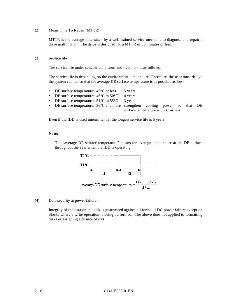
(3) Service life
The service life under suitable conditions and treatment is as follows.
The service life is depending on the environment temperature. Therefore, the user must designthe system cabinet so that the average DE surface temperature is as possible as low.
• DE surface temperature: 45°C or less 5 years• DE surface temperature: 46°C to 50°C 4 years• DE surface temperature: 51°C to 55°C 3 years• DE surface temperature: 56°C and more strengthen cooling power so that DE
surface temperature is 55°C or less.
Even if the IDD is used intermittently, the longest service life is 5 years.
Note:
The "average DE surface temperature" means the average temperature at the DE surfacethroughout the year when the IDD is operating.
(4) Data security at power failure
Integrity of the data on the disk is guaranteed against all forms of DC power failure except onblocks where a write operation is being performed. The above does not applied to formattingdisks or assigning alternate blocks.
C141-E035-01EN 2 - 7
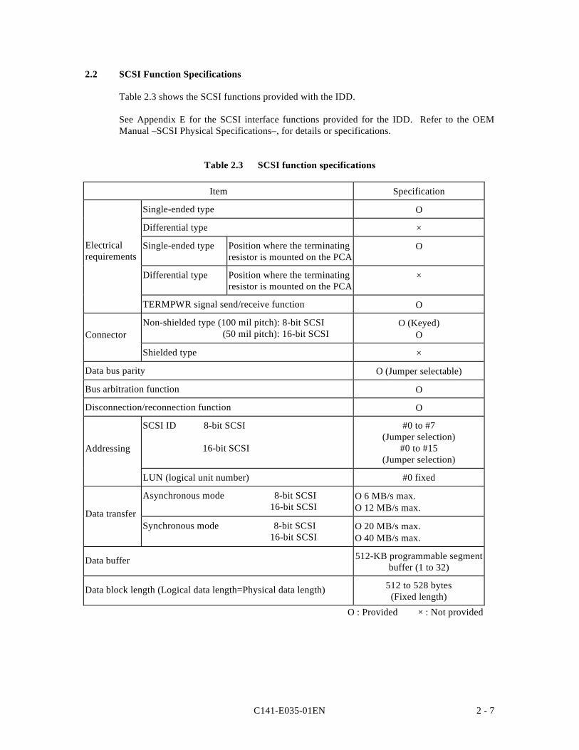
2.2 SCSI Function Specifications
Table 2.3 shows the SCSI functions provided with the IDD.
See Appendix E for the SCSI interface functions provided for the IDD. Refer to the OEMManual –SCSI Physical Specifications–, for details or specifications.
Table 2.3 SCSI function specifications
Item Specification
Single-ended type Ο
Differential type ×
Single-ended type Position where the terminatingresistor is mounted on the PCA
Ο
Differential type Position where the terminatingresistor is mounted on the PCA
×
TERMPWR signal send/receive function Ο
Non-shielded type (100 mil pitch): 8-bit SCSI (50 mil pitch): 16-bit SCSI
Ο (Keyed)Ο
Shielded type ×
Data bus parity Ο (Jumper selectable)
Bus arbitration function Ο
Disconnection/reconnection function Ο
SCSI ID 8-bit SCSI
16-bit SCSI
#0 to #7(Jumper selection)
#0 to #15(Jumper selection)
LUN (logical unit number) #0 fixed
Asynchronous mode 8-bit SCSI 16-bit SCSI
Ο 6 MB/s max.Ο 12 MB/s max.
Synchronous mode 8-bit SCSI 16-bit SCSI
Ο 20 MB/s max.Ο 40 MB/s max.
Data buffer 512-KB programmable segmentbuffer (1 to 32)
Data block length (Logical data length=Physical data length) 512 to 528 bytes(Fixed length)
Ο : Provided × : Not provided
Data transfer
Addressing
Connector
Electricalrequirements

C141-E035-01EN 3 - 1
CHAPTER 3 DATA FORMAT
3.1 Data Space
3.2 Logical Data Block Addressing
3.3 Defect Management
This chapter explains data space definition, logical data block addressing, and defect management onthe IDD.
3.1 Data Space
The IDD manages the entire data storage area divided into the following three data spaces.
• User space: Storage area for user data
• Internal test space: Reserved area for diagnostic purposes
• System space: Area for exclusive use of IDD itself
The user space allow a user access by specifying data. These space can be accessed with thelogical data block addressing method described in Section 3.2. The internal test space is usedby Read/write test of self-diagnostics test, but user can’t use direct access. The system space isaccessed inside the IDD at power-on or during the execution of a specific command, but theuser cannot directly access the system space.
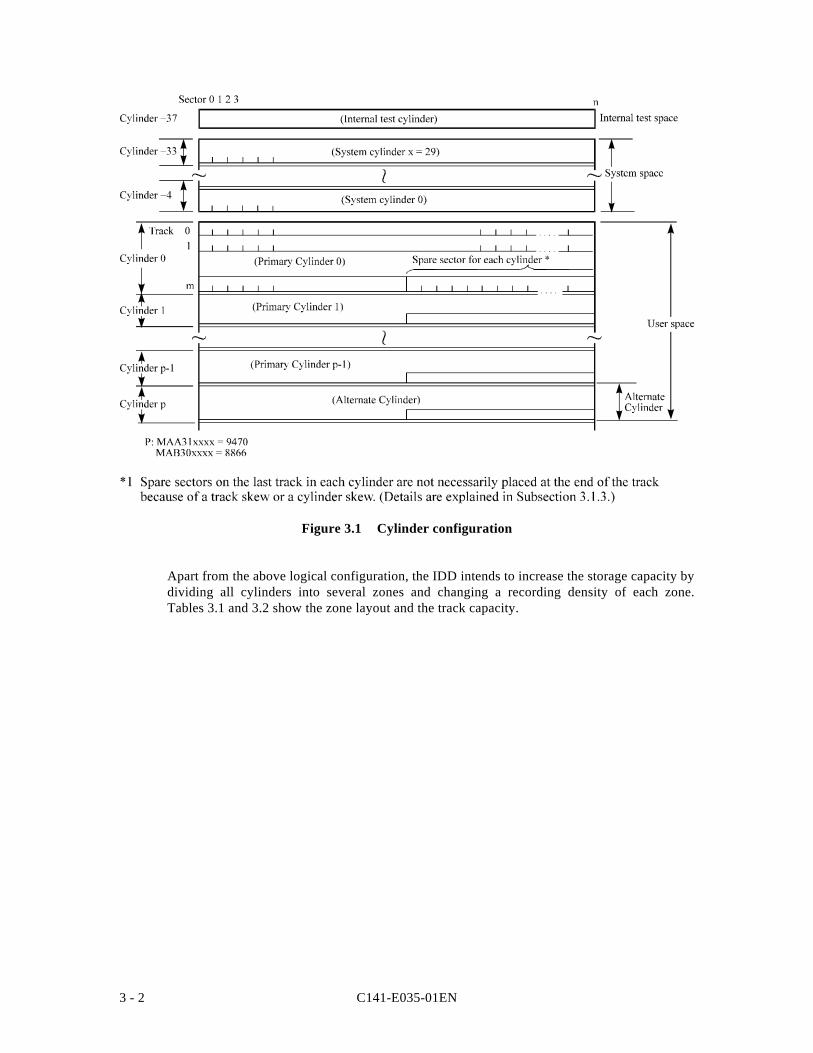
3.1.1 Cylinder configuration
The IDD allocates cylinders to the user space, Internal test space, and system space. Figure3.1 is the cylinder configuration.
Spare areas (alternate areas) for defective sectors are provided in the user space. Severalsectors in the last track of one cylinder and several cylinders (alternate cylinders) in the userspace are allocated as alternate areas according to the user's assignment (MODE SELECTcommand). See Subsection 3.1.2 for details.
C141-E035-01EN3 - 2
Figure 3.1 Cylinder configuration
Apart from the above logical configuration, the IDD intends to increase the storage capacity bydividing all cylinders into several zones and changing a recording density of each zone.Tables 3.1 and 3.2 show the zone layout and the track capacity.
C141-E035-01EN 3 - 3
Table 3.1 Zone layout and track capacity (MAA31xxxx)
Zone 0 1 2 3 4 5 6
Cylinder 0 to 1,039 1,040 to1,885
1,886 to2,725
2,726 to3,560
3,561 to4,389
4,390 to5,017
5,018 to5,916
Byte/track 146,666 ← ← 145,833 141,666 136,666 130,000
Sector/track 224 ← ← 222 216 208 200
Zone 7 8 9 10 11 12 13
Cylinder 5,917 to6,538
6,539 to7,352
7,353 to7,932
7,933 to8,202
8,203 to8,865
8,866 to9,231
9,232 to9,470
Byte/track 125,000 118,333 112,500 110,000 102,500 98,333 95,000
Sector/track 190 180 170 166 160 148 144
Table 3.2 Zone layout and track capacity (MAB30xxxx)
Zone 0 1 2 3 4 5 6
Cylinder 0 to 1,039 1,040 to1,885
1,886 to2,725
2,726 to3,560
3,561 to4,389
4,390 to5,017
5,018 to5,916
Byte/track 146,666 ← ← 145,833 141,666 136,666 130,000
Sector/track 186 186 182 180 178 174 170
Zone 7 8 9 10 11
Cylinder 5,917 to6,538
6,539 to7,352
7,353 to7,932
7,933 to8,202
8,203 to8,866
Byte/track 125,000 118,333 112,500 110,000 102,500
Sector/track 190 180 170 166 160
(1) User space
The user space is a storage area for user data. The data format on the user space (the length ofdata block and the number of data blocks) can be specified with the MODE SELECT orMODE SELECT EXTENDED command.
The default number of cylinders in the user space is 9,471 for MAA31xxxx and 8,867 forMAB30xxxx. The user, however, can select the number of cylinders to be allocated in the userspace by specifying 9,471 for MAA31xxxx and 8,867 for MAB30xxxx as the maximum andthe number of alternate cylinders + 1 as the minimum. The user can also specify the numberof logical data blocks to be placed in the user space with the MODE SELECT or MODESELECT EXTENDED command. When the number of logical data blocks is specified, asmany cylinders as required to place the specified data blocks are allocated in the user space.
C141-E035-01EN3 - 4
A number starting with 0 is assigned to each cylinder required in the user space in ascendingorder. If the number does not reach 9,471 (MAA31xxxx) and 8,867 (MAB30xxxx), the restof the cylinders will not be used.
Always one alternate cylinders can be established in the user space. Alternate cylinders willbe used for alternate blocks when primary cylinders in the user space and spare sectors in thecylinder in the CE space are used up. See Subsections 3.1.2 and 3.3.2 for details.
(2) Internal test space
The Internal test space is an area for diagnostic purposes only and its data block length isalways 512KByte. The Internal test space consists of only 1 cylinder and outer-host cylinderis always assigned. The user cannot change the number of cylinders in the Internal test spaceor their positions.
The IDD reads or writes the data block in the CE space during the self-diagnostic test specifiedwith the setting terminal (diagnostic mode) or a SEND DIAGNOSTIC command.
(3) System space
The system space is an area for exclusive use of the IDD itself and the following informationare recorded. The length of the data block is always 512 bytes.
• Defect list (P list and G list)• MODE SELECT parameter (saved value)• Statistical information (log data)• Controller control information
The above information are duplicated in several different locations for safety.
Note:
The system space is also called SA space.
C141-E035-01EN 3 - 5
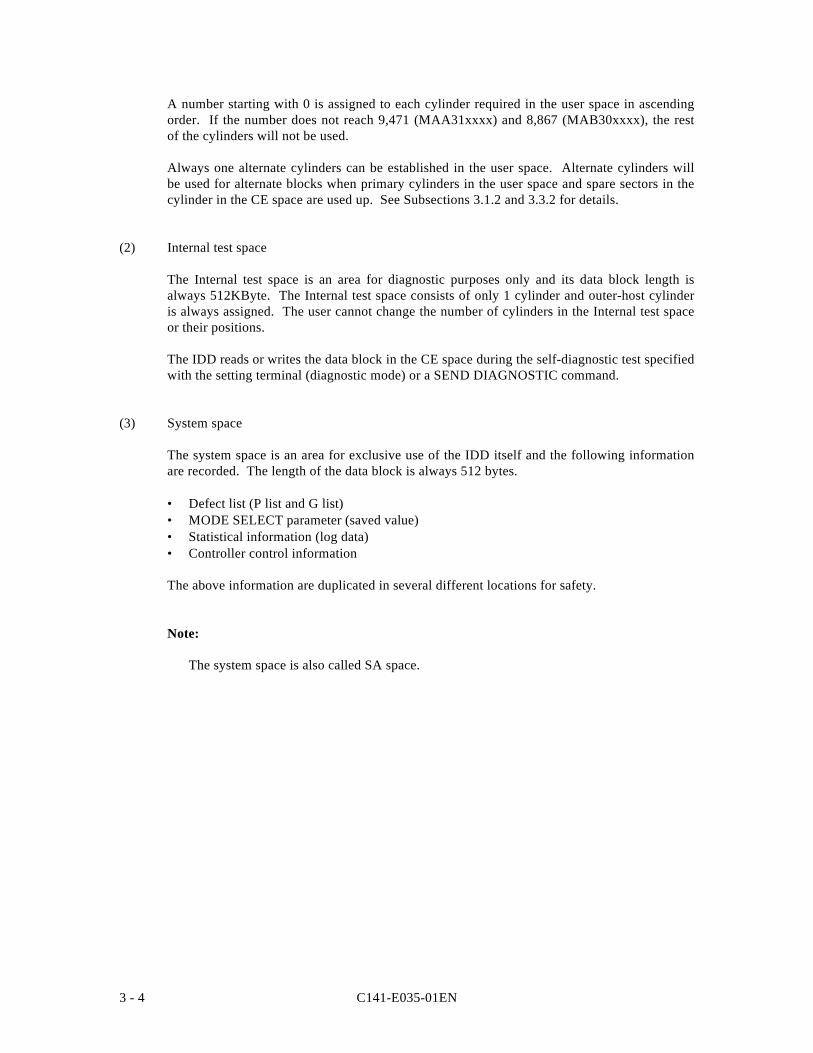
3.1.2 Alternate spare area
The alternate spare area is provided in the last track of each primary cylinder in the user space,and in the last track of the cylinder and the alternate cylinder.
The spare area in each cylinder is placed at the end of the last track as shown in Figure 3.2.These spare sectors are located in the end of the track logically, not necessarily located at theend physically because of track skew or cylinder skew. (Details are explained on Subsection3.1.3.)
Size can be specified by the MODE SELECT command.
The number of spare sectors per cylinder can be specified exceeding 32. The default value ofnumber of 9space sectors per cylinder is 20.
Figure 3.2 Spare area in cylinders
An alternate cylinder is used when spare sectors in a cylinder are used up or 0 is specified asthe number of spare sectors in a cylinder. Several cylinders at the end of the user space areallocated as alternate cylinders as shown in Figure 3.3.
The number of alternate cylinder is 1.
The user space and the CE space share the alternate cylinders.
Figure 3.3 Alternate cylinder
Note:
Zero cannot be specified for both the number of spare sectors in each cylinder and thenumber of alternate cylinders.
C141-E035-01EN3 - 6
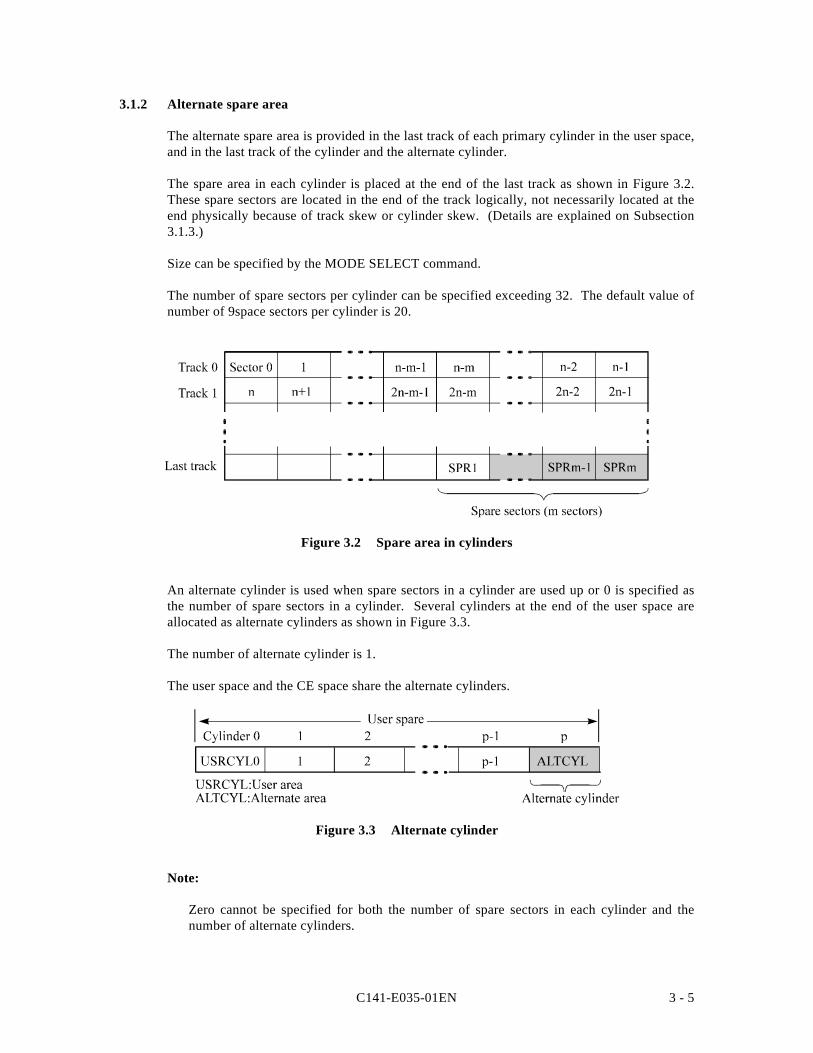
3.1.3 Track format
(1) Physical sector allocation
Figure 3.4 shows the allocation of the physical sectors in a track. The length in bytes of eachphysical sector and the number of sectors per track vary depending on the logical data blocklength. The unused area (G4) exists at the end of the track in formats with most logical datablock lengths.
The interval of the sector pulse (length of the physical sector) is decided by multiple of15MHz free running frequency. This clock is not equal to the interval of the byte clock foreach zone. Therefore, the physical sector length cannot be described with a byte length.
Figure 3.4 Track format
C141-E035-01EN 3 - 7
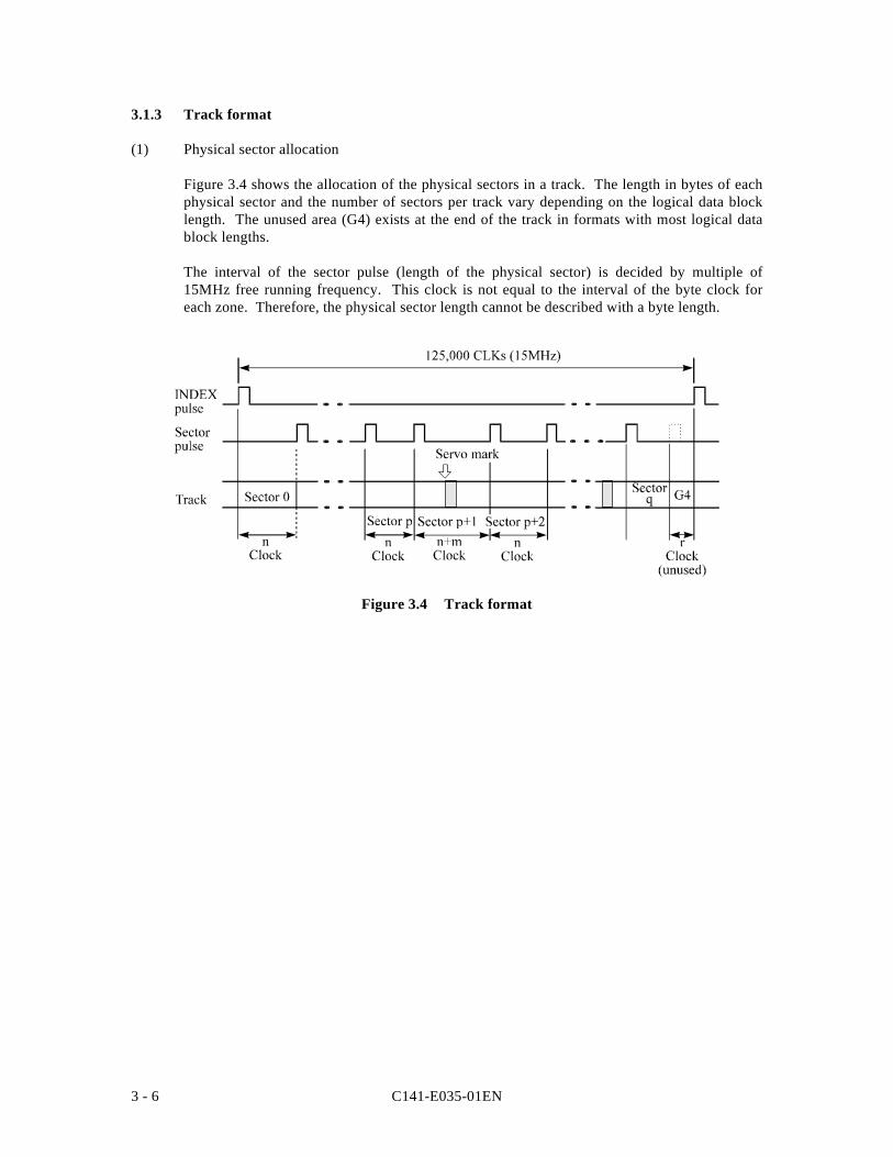
(2) Track skew and cylinder skew
To avoid waiting for one turn involved in head and cylinder switching, the first logical datablock in each track is shifted by the number of sectors (track skew and cylinder skew)corresponding to the switching time. Figure 3.5 shows how the data block is allocated in eachtrack.
At the head switching location in a cylinder, the first logical data block in track t + 1 isallocated at the sector position which locates the track skew behind the sector position of thelast logical data block sector in track t.
At the cylinder switching location, like the head switching location, the first logical data blockin a cylinder is allocated at the sector position which locates the cylinder skew behind the lastlogical sector position in the preceding cylinder. The last logical sector in the cylinder isallocated when formatting, and is an unused spare sector.
Figure 3.5 Track skew/cylinder skew
The number of physical sectors (track skew factor and cylinder skew factor) corresponding tothe skew time varies depending on the logical data block length because the track skew andthe cylinder skew are managed for individual sectors. The IDD automatically determinesappropriate values for the track skew factor and the cylinder skew factor according to thespecified logical data block length. The value can be read out by the MODE SENSE orMODE SENSE EXTENDED command after the track has been formatted.
C141-E035-01EN3 - 8
3.1.4 Sector format
Each sector on the track consists of an ID field, a data field, and a gap field which separatesthem. Figure 3.6 gives sector format examples.
Figure 3.6 Sector format
Each sector on the track consists of the following fields:
(1) Gaps (G1)
The gap length at the time of formatting (initializing) is listed in Figure 3.6. Pattern X'00' iswritten on the gap field.
(2) PLO Sync
In this field, pattern X'00' in the length in bytes listed in Figure 3.6 is written.
(3) Trailing (TRNG)/Sync Byte (SB)
In this field, special pattern in the length in bytes listed in Figure 3.6 is written.
(4) LBA
The logical block address is written in this field.

C141-E035-01EN 3 - 9
(5) Data field
User data is stored in the data field of the sector. The length of the data field is equal to that ofthe logical data block which is specified with a parameter in the MODE SELECT command.Any even number between 512 and 528 bytes can be specified as the length.
(6) BCRC
It is a 2-byte error detection code. Errors in the ID field. Single burst errors with lengths of upto 16 bits for each logical block can be detected.
(7) ECC
24-byte data error detection/correction code for the data field. It is possible to on-the-flycorrect the single burst errors with lengths of up to 89 bits.
(8) PAD 1
A specified length of x‘00’ pattern shown in Figure 3.6 is written in this field. This fieldincludes the variation by rotation and circuit delay till reading/writing.
(9) PAD 2
A specified length of x‘00’ pattern shown in Figure 3.6 is written in this field. This fieldcontains the processing time necessary to process next sector continuously. This field haverotational speed variation.
(10) SPAD
A specified length of X‘00’ pattern shown in Figure 3.6 is written in this field. This fieldcontains the processing time necessary at the ECC control circuit when the logical blocklength exceeds 734 bytes and is divided into several subsectors.

C141-E035-01EN3 - 10
3.1.5 Format capacity
The size of the usable area for storing user data on the IDD (format capacity) varies accordingto the logical data block or the size of the spare sector area. Table 3.3 lists examples of theformat capacity when the typical logical data block length and the default spare area are used.The following is the general formula to calculate the format capacity.
[Format capacity] = [number of sectors per track × number of tracks (heads) – number ofalternate spare sectors per cylinder] × [number of cylinders in user space – number of alternatecylinders] × [number of physical sectors in logical block] × [logical data block length]
The following formula must be used when the number of logical data blocks are specified withthe parameter in the MODE SELECT or MODE SELECT EXTENDED command.
[Format capacity] = [logical data block length] × [number of logical data blocks]
The logical data block length, the maximum logical block address, and the number of thelogical data blocks can be read out by a READ CAPACITY, MODE SENSE, or MODESENSE EXTENDED command after initializing the disk medium.
Table 3.3 Format capacity
Model Data heads Data block length User blocks Format capacity (MB)
MAA3182xx 19 512 35,675,874 18,266,047,488
MAB3091xx 10 512 17,819,500 9,123,584,000
MAB3045xx 5 512 8,821,090 4,516,398,080
MAB3024xx 3 512 5,221,726 2,673,523,712
Note:
Total number of spare sectors is calculated by adding the number of spare sectors in eachprimary cylinder and the number of sectors in the alternate cylinders.
C141-E035-01EN 3 - 11
3.2 Logical Data Block Addressing
Independently of the physical structure of the disk drive, the IDD adopts the logical data blockaddressing as a data access method on the disk medium. The IDD relates a logical data blockaddress to each physical sector at formatting. Data on the disk medium is accessed in logicaldata block units. The INIT specifies the data to be accessed using the logical data blockaddress of that data.
The logical data block addressing is a function whereby individual data blocks are givenaddresses of serial binaries in each drive.
(1) Block address of user space
The logical data block address number is consecutively assigned to all of the data blocks in theuser space starting with 0 to the first data block.
The IDD treats sector 0, track 0, cylinder 0 as the first logical data block. The data block isallocated in ascending order of addresses in the following sequence (refer to Figure 3.5):
1) Numbers are assigned in ascending order to all sectors in the same track.
2) By following step 1), numbers are assigned in ascending order of tracks to all sectors ineach track in the same cylinder except the last track.
3) By following step 1), numbers are assigned to all sectors in the last track except the sparesectors.
4) After completing steps 1) through 3) for the same cylinder, this allocation is repeated fromtrack 0 in the next cylinder and on to the last cylinder (cylinder p-q in Figure 3.1) exceptfor the alternate cylinders in ascending order of cylinder numbers.
When the logical data block is allocated, some sectors (track skew and cylinder skew) shownin Figure 3.5 are provided to avoid waiting for one turn involving head and cylinder switchingat the location where the track or the cylinder is physically switched.
See Subsection 3.3.2 for defective/alternate block treatment and the logical data blockallocation method in case of defective sectors exist on the disk.
(2) Alternate area
Alternate areas in the user space (spare sectors in the cylinder and alternate cylinders) are notincluded in the above logical data block addresses. Access to sectors which are allocated as analternate block in the alternate area is made automatically by means of IDD sector sliptreatment or alternate block treatment (explained in Subsection 3.3.2), so the user does nothave to worry about accessing the alternate area. The user cannot access with specifying thedata block on the alternate area explicitly.
C141-E035-01EN3 - 12
3.3 Defect Management
3.3.1 Defect list
Information of the defect location on the disk is managed by the defect list. The following aredefect lists which the IDD manages.
• P list (Primary defect list): This list consists of defect location information available at thedisk drive shipment and is recorded in a system space. The defects in this list arepermanent, so the INIT must execute the alternate block allocation using this list wheninitializing the disk.
• D list (Data defect list): This list consists of defect location information specified in aFORMAT UNIT command by the INIT at the initialization of the disk. This informationis recorded in the system space of the disk drive as the G list. To execute the alternateblock allocation, the FORMAT UNIT command must be specified.
• C list (Certification defect list): This list consists of location information on defectiveblocks which are detected by the verifying operation (certification) of the data block afterthe initiation when executing the FORMAT UNIT command. The IDD generates thisinformation when executing the FORMAT UNIT command, and the alternate blockallocation is made upon the defective block. This information is recorded in the systemspace of the disk drive as the G list.
• G list (Growth defect list): This list consists of defective logical data block locationinformation specified in a REASSIGN BLOCKS command by the INIT, information ondefective logical data blocks assigned alternate blocks by means of IDD automaticalternate block allocation, information specified as the D list, and information generated asthe C list. They are recorded in the system space on the disk drive.
The INIT can read out the contents of the P and G lists by the READ DEFECT DATA command.
3.3.2 Alternate block allocation
The alternate data block is allocated to a defective data block (= sectors) in defective sectorunits by means of the defect management method inside the IDD.
The INIT can access all logical data blocks in the user space, as long as there is no error.
Spare sectors to which alternate blocks are allocated can be provided in either "spare sectors ina cylinder" or "alternate cylinders". See Subsection 3.1.2 for details.
The INIT can specify the size and area for spare sectors by the MODE SELECT command atthe time of the initialization of the disk.
Both of the following are applicable to the alternate block allocation.
• Sector slip treatment: Defective sectors are skipped and the logical data blockcorresponding to those sectors is allocated to the next physical sectors. This treatment ismade on the same cylinder as the defective sector's and is effective until all spare sectors inthat cylinder are used up.
C141-E035-01EN 3 - 13
• Alternate sector treatment: The logical data block corresponding to defective sectors isallocated to unused spare sectors in the same cylinder or unused spare sectors in thealternate cylinder.
The alternate block allocation is executed by the FORMAT UNIT command, the REASSIGNBLOCKS command, or the automatic alternate block allocation. Refer to OEM Manual–SCSILogical Specifications–for details of specifications on these commands. The logical datablock is allocated to the next physically continued sectors after the above sector slip treatmentis made. On the other hand, the logical data block is allocated to spare sectors which are notphysically consecutive to the adjacent logical data blocks. If a command which processesseveral logical data blocks is specified, the IDD processes those blocks in ascending order oflogical data block.
(1) Alternate block allocation during FORMAT UNIT command execution
When the FORMAT UNIT command is specified, the allocation of the alternate block to thosedefective sectors included in the specified lists (P, G, or D) is continued until all spare sectorsin the same cylinder are used up. When they are used up, unused spare sectors in the alternatecylinder are allocated to the subsequent sectors in the cylinder by means of alternate sectortreatment. Figure 3.7 is examples of the alternate block allocation during the FORMAT UNITcommand execution.
C141-E035-01EN3 - 14
Figure 3.7 Alternate block allocation by FORMAT UNIT command
If the data block verifying operation (certification) is not permitted (DCRT flag = 0) in theFORMAT UNIT command, the IDD checks all initialized logical data blocks by reading themout after the above alternate block allocation is made to initialize (format) the disk. If adefective data block is detected during the check, the IDD generates the C list for defectlocation information and allocates the alternate block to the defective data block. Thisalternate block allocation is made by means of alternate sector treatment only like processingby the REASSIGN BLOCKS command even if unused spare sectors exists in the samecylinder.
: Unused spare sector
: Defective sector
: n represents a logical data block number
C141-E035-01EN 3 - 15
(2) Alternate block allocation by REASSIGN BLOCKS command
When the REASSIGN BLOCKS command is specified, the alternate block is allocated to thedefective logical data block specified by the initiator by means of alternate sector treatment. Ifthere are unused spare sectors in the same cylinder as the specified defective logical datablock, the alternate block is allocated to these unused spare sectors. However, the alternateblock is allocated to unused spare sectors in the alternate cylinder when all spare sectors in thecylinder are used up.
Figure 3.8 is examples of the alternate block allocation by the REASSIGN BLOCKScommand.
Figure 3.8 Alternate block allocation by REASSIGN BLOCKS command
: Unused spare sector
: Defective sector
: n represents a logical data block number
C141-E035-01EN3 - 16
(3) Automatic alternate block allocation
If the ARRE flag in the MODE SELECT parameter permits the automatic alternate blockallocation, the IDD automatically executes the alternate block allocation and data duplicationon the defective data block detected during the READ EXTENDED command. Thisallocation method is the same as with the REASSIGN BLOCKS command (alternate sectortreatment).
IMPORTANT
Automatic alternate block allocation is made only once during theexecution of one command. If second defective block is detected,the alternate block assignment processing for the first defectiveblock is executed but the alternate block assignment processingfor the second one is not executed and the command beingexecuted terminates. However, the initiator can recover the twiceerror by issuing the same command again.
When an error is detected in a data block in the data area,recovery data is rewritten and verified in automatic alternateblock allocation during the execution of the READ or READEXTENDED command. Alternate block allocation will not bemade for the data block if recovery is successful.
Example: Even if the data error which is recoverable by theWRITE LONG command is simulated, automaticalternate block allocation will not be made for the datablock.
C141-E035-01EN 4 - 1
CHAPTER 4 INSTALLATION REQUIREMENTS
4.1 Mounting Requirements
4.2 Power Supply Requirements
4.3 Connection Requirements
This chapter describes the environmental, mounting, power supply, and connection requirements.
4.1 Mounting Requirements
4.1.1 External dimensions
Figures 4.1 and 4.2 show the external dimensions of the IDD and the positions of the holes forthe IDD mounting screws.
Note:
Dimensions are in mm.
C141-E035-01EN4 - 2
Figure 4.1 External dimensions (MAA3xxx)
(*) Between mounting screwon the bottom.
C141-E035-01EN 4 - 3
Figure 4.2 External dimensions (MAB3xxx)
C141-E035-01EN4 - 4
4.1.2 Mounting
The permissible orientations of the IDD are shown in Figure 4.3, and the tolerance of the angleis ±5° from the horizontal plane.
Figure 4.3 IDD orientation
4.1.3 Notes on mounting
(1) Mounting frame structure
To guarantee integrity of the IDD disk enclosure (DE) insulation once mounted on the frameinside the system, special attention must be given to the note below.
Note:
Generally, SG and FG are connected at one point in the system enclosure. Therefore, usefollowing procedure to maintain the insulation when mounting the IDD.
a) Use the frame with an embossed structure or the like to avoid contact between the DEbase and FG. Mount the IDD with making a gap of 2.5 mm or more between the IDDand the frame of the system.
b) As shown in Figure 4.4, the inward projection of the screw from the IDD frame wallat the corner must be 4 mm or less.
Direction ofgravity
(a) Horizontal –1 (b) Horizontal –2 (c) Vertical –1
(d) Vertical –2 (e) Upright mounting –1 (f) Upright mounting –2
C141-E035-01EN 4 - 5
c) To avoid tap from broken, tighten torque of screw is less than 5 kg•cm.
Damage : To absolutely guarantee integrity of the IDD disk enclosure (DE) insulationonce actually mounted to the frame inside the system, special attention must be givento the cautionary notes below.
Figure 4.4 Mounting frame structure
(2) Limitation of side-mounting
Mount the side using the screw holes at both the ends as shown in Figure 4.5. Do not use thecenter hole.
Figure 4.5 Limitation of side-mounting
Use these holes
Do not use these holes

C141-E035-01EN4 - 6
(3) Environmental temperature
Temperature condition at installed in a cabinet is indicated with ambient temperature measured3 cm from the disk drive. At designing the system cabinet, consider following points.
• Make a suitable air flow so that the DE surface temperature does not exceed 55°C.
• Cool the PCA side especially with air circulation inside the cabinet. Confirm the coolingeffect by measuring temperature of specific ICs and the DE. These measurement resultsshould be within a criteria listed in Table 4.1.
Table 4.1 Surface temperature check point
No. Measurement point Criteria
1 Center of DE cover 55°C
2 Read channel LSI 80°C
3 DSP LSI 75°C
4 HDC 80°C
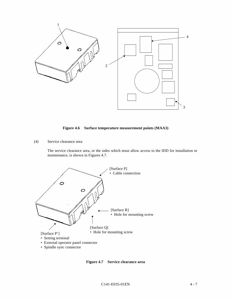
C141-E035-01EN 4 - 7
Figure 4.6 Surface temperature measurement points (MAA3)
(4) Service clearance area
The service clearance area, or the sides which must allow access to the IDD for installation ormaintenance, is shown in Figures 4.7.
Figure 4.7 Service clearance area
4
3
2
1
[Surface P]• Cable connection
[Surface R]• Hole for mounting screw
[Surface Q]• Hole for mounting screw[Surface P’]
• Setting terminal• External operator panel connector• Spindle sync connector
C141-E035-01EN4 - 8
(5) External magnetic field
The drive should not be installed near the ferromagnetic body like a speaker to avoid theinfluence of the external magnetic field.
(6) Leak magnetic flux
The IDD uses a high performance magnet to achieve a high speed seek. Therefore, a leakmagnetic flux at surface of the IDD is large. Mount the IDD so that the leak magnetic fluxdoes not affect to near equipment.
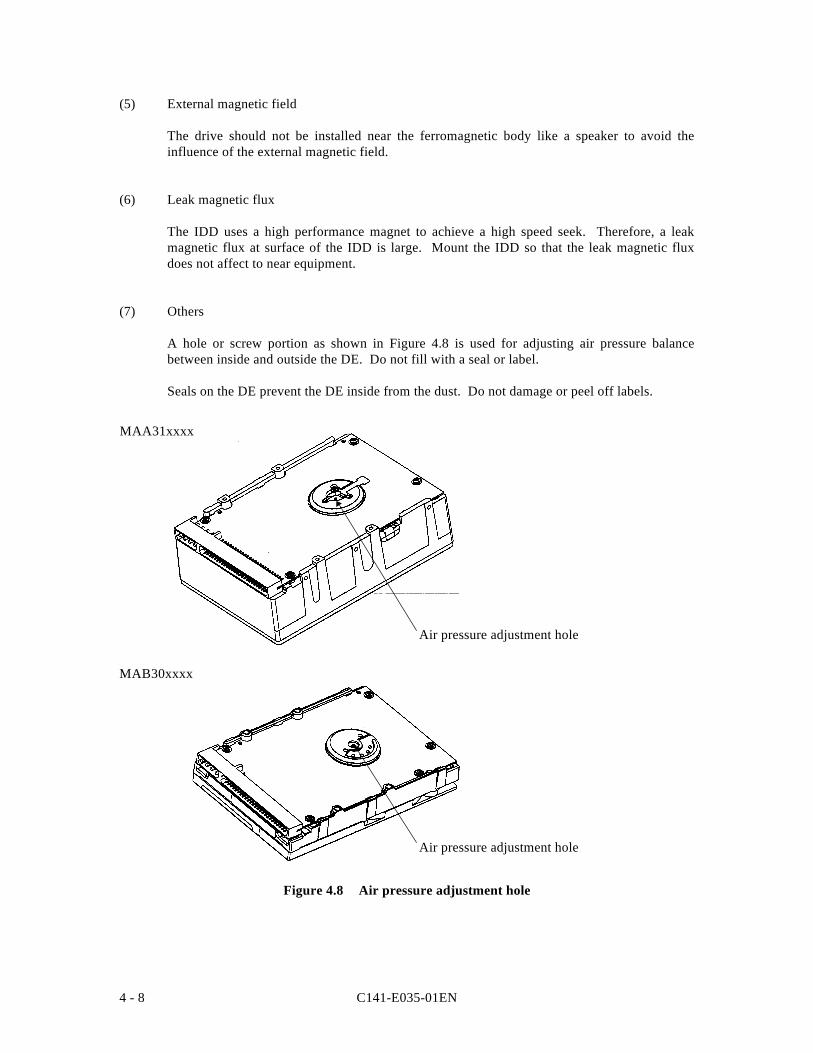
(7) Others
A hole or screw portion as shown in Figure 4.8 is used for adjusting air pressure balancebetween inside and outside the DE. Do not fill with a seal or label.
Seals on the DE prevent the DE inside from the dust. Do not damage or peel off labels.
MAB30xxxx
Figure 4.8 Air pressure adjustment hole
Air pressure adjustment hole
MAA31xxxx
Air pressure adjustment hole
C141-E035-01EN 4 - 9
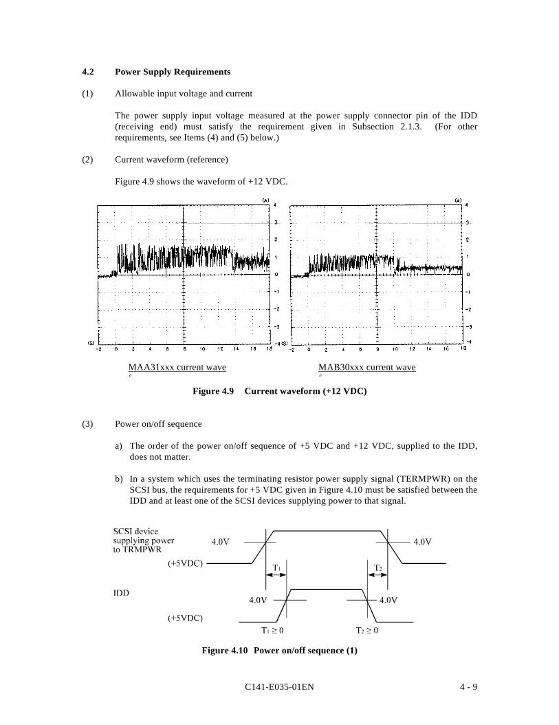
4.2 Power Supply Requirements
(1) Allowable input voltage and current
The power supply input voltage measured at the power supply connector pin of the IDD(receiving end) must satisfy the requirement given in Subsection 2.1.3. (For otherrequirements, see Items (4) and (5) below.)
(2) Current waveform (reference)
Figure 4.9 shows the waveform of +12 VDC.
Figure 4.9 Current waveform (+12 VDC)
(3) Power on/off sequence
a) The order of the power on/off sequence of +5 VDC and +12 VDC, supplied to the IDD,does not matter.
b) In a system which uses the terminating resistor power supply signal (TERMPWR) on theSCSI bus, the requirements for +5 VDC given in Figure 4.10 must be satisfied between theIDD and at least one of the SCSI devices supplying power to that signal.
Figure 4.10 Power on/off sequence (1)
MAB30xxx current waveform
MAA31xxx current waveform
C141-E035-01EN4 - 10
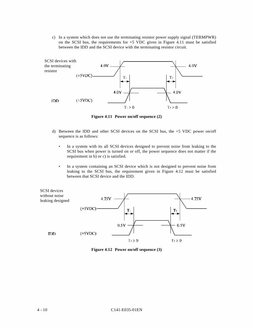
c) In a system which does not use the terminating resistor power supply signal (TERMPWR)on the SCSI bus, the requirements for +5 VDC given in Figure 4.11 must be satisfiedbetween the IDD and the SCSI device with the terminating resistor circuit.
Figure 4.11 Power on/off sequence (2)
d) Between the IDD and other SCSI devices on the SCSI bus, the +5 VDC power on/offsequence is as follows:
• In a system with its all SCSI devices designed to prevent noise from leaking to theSCSI bus when power is turned on or off, the power sequence does not matter if therequirement in b) or c) is satisfied.
• In a system containing an SCSI device which is not designed to prevent noise fromleaking to the SCSI bus, the requirement given in Figure 4.12 must be satisfiedbetween that SCSI device and the IDD.
Figure 4.12 Power on/off sequence (3)
SCSI deviceswithout noiseleaking designed
SCSI devices withthe terminatingresistor
C141-E035-01EN 4 - 11
(4) Sequential starting of spindle motors
After power is turned on to the IDD, a large amount of current flows in the +12 VDC linewhen the spindle motor rotation starts. Therefore, if more than one IDD is used, the spindlemotors should be started sequentially using one of the following procedures to preventoverload of the power supply unit. For how to set a spindle motor start control mode, seeSubsection 5.3.2.
a) Issue START/STOP commands at 20-second intervals to start the spindle motors. Fordetails of this command specification, refer to OEM Manual –SCSI LogicalSpecifications–.
b) Turn on the +12 VDC power in the power supply unit at 20-second intervals to start thespindle motors sequentially.
(5) Power supply to SCSI terminating resistor
If power for the terminating resistor is supplied from the IDD to other SCSI devices throughthe SCSI bus, the current-carrying capacity of the +5 VDC power supply line to the IDD mustbe designed with considering of an increase of up to 200 mA.
A method of power supply to the terminating resistor is selected with a setting terminal on theIDD. See Subsection 5.3.2 for this selection.
For the electrical condition of supplying power to the terminating resistor, refer to Subsection1.4.2 in OEM Manual –SCSI Physical Specifications–.
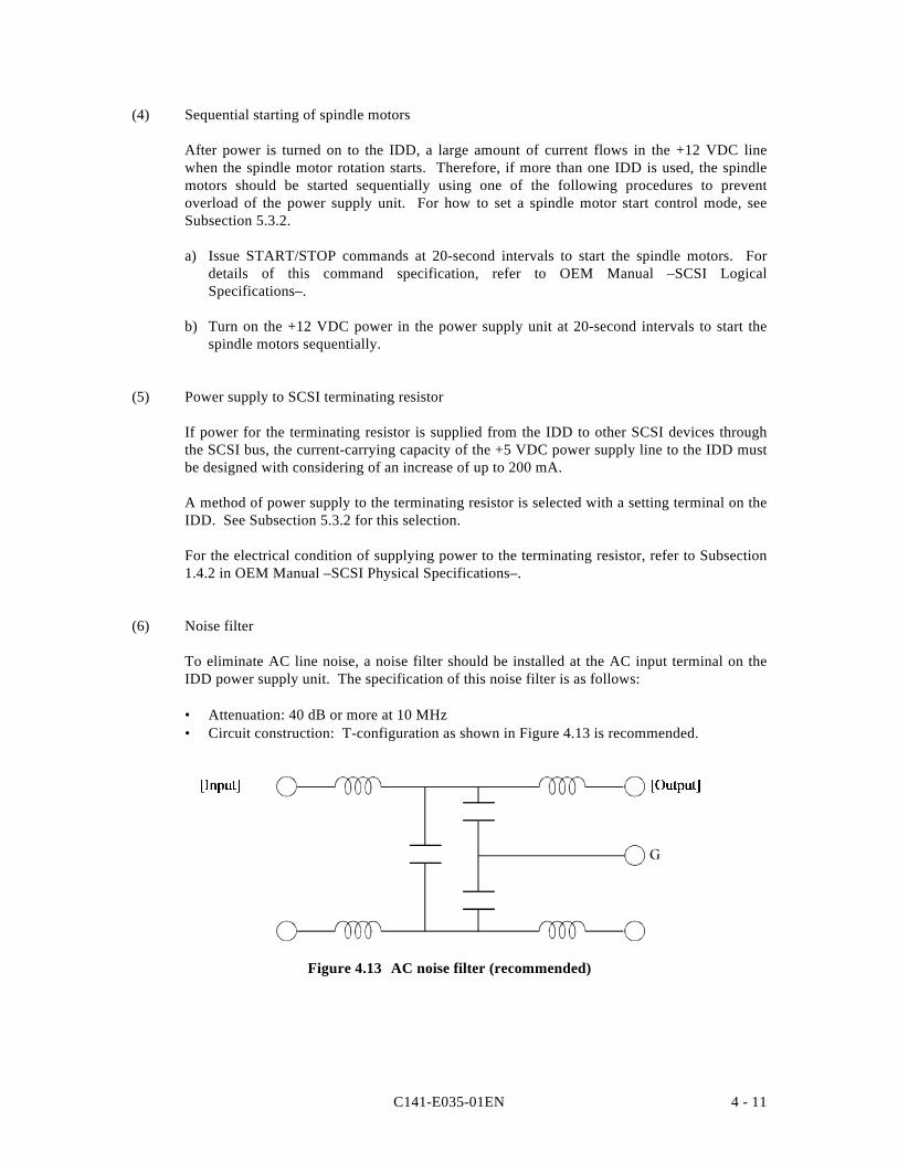
(6) Noise filter
To eliminate AC line noise, a noise filter should be installed at the AC input terminal on theIDD power supply unit. The specification of this noise filter is as follows:
• Attenuation: 40 dB or more at 10 MHz• Circuit construction: T-configuration as shown in Figure 4.13 is recommended.
Figure 4.13 AC noise filter (recommended)
C141-E035-01EN4 - 12
4.3 Connection Requirements
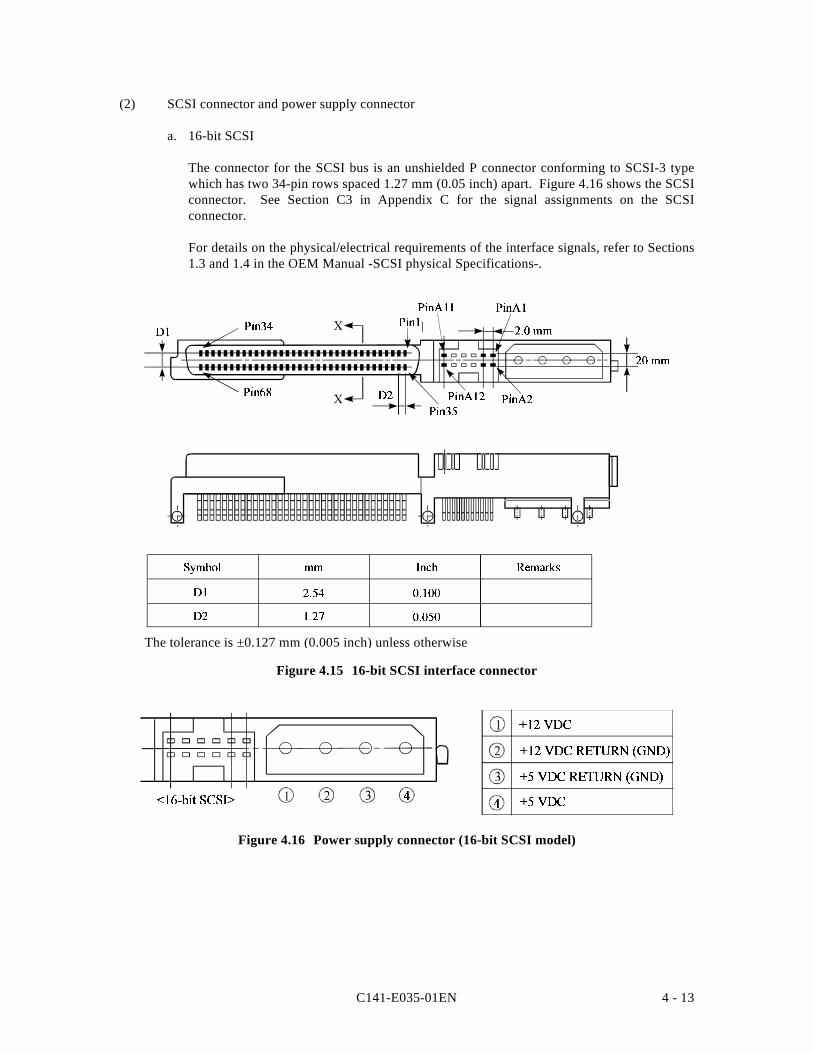
4.3.1 16-bit SCSI model (MAA31xxxSP, MAB30xxxSP)
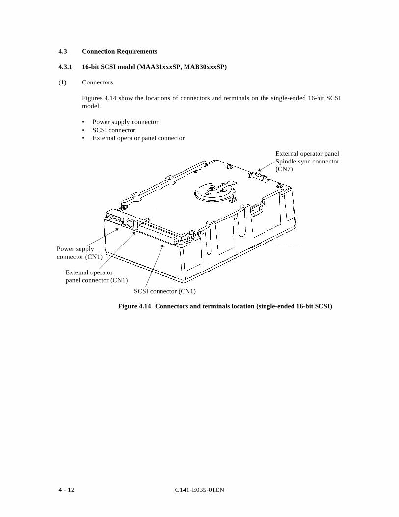
(1) Connectors
Figures 4.14 show the locations of connectors and terminals on the single-ended 16-bit SCSImodel.
• Power supply connector• SCSI connector• External operator panel connector
Figure 4.14 Connectors and terminals location (single-ended 16-bit SCSI)
SCSI connector (CN1)
External operator panelSpindle sync connector(CN7)
External operatorpanel connector (CN1)
Power supplyconnector (CN1)
C141-E035-01EN 4 - 13
(2) SCSI connector and power supply connector
a. 16-bit SCSI
The connector for the SCSI bus is an unshielded P connector conforming to SCSI-3 typewhich has two 34-pin rows spaced 1.27 mm (0.05 inch) apart. Figure 4.16 shows the SCSIconnector. See Section C3 in Appendix C for the signal assignments on the SCSIconnector.
For details on the physical/electrical requirements of the interface signals, refer to Sections1.3 and 1.4 in the OEM Manual -SCSI physical Specifications-.
Figure 4.15 16-bit SCSI interface connector
Figure 4.16 Power supply connector (16-bit SCSI model)
The tolerance is ±0.127 mm (0.005 inch) unless otherwise
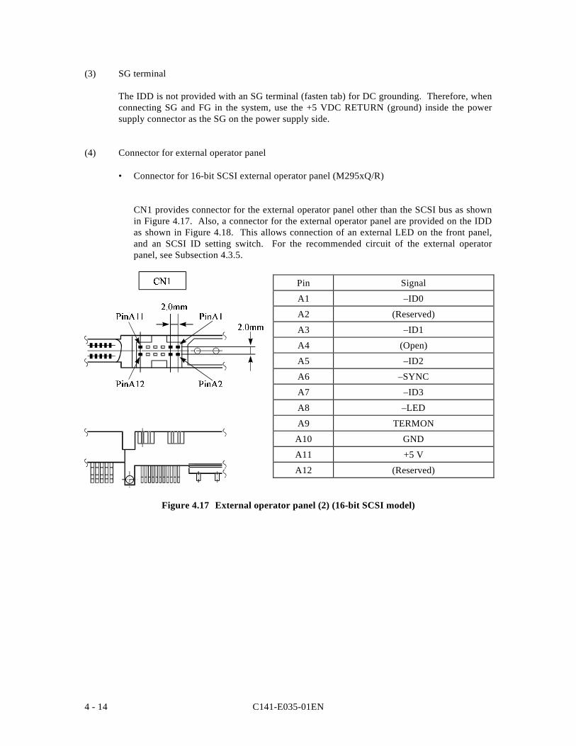
C141-E035-01EN4 - 14
(3) SG terminal
The IDD is not provided with an SG terminal (fasten tab) for DC grounding. Therefore, whenconnecting SG and FG in the system, use the +5 VDC RETURN (ground) inside the powersupply connector as the SG on the power supply side.
(4) Connector for external operator panel
• Connector for 16-bit SCSI external operator panel (M295xQ/R)
CN1 provides connector for the external operator panel other than the SCSI bus as shownin Figure 4.17. Also, a connector for the external operator panel are provided on the IDDas shown in Figure 4.18. This allows connection of an external LED on the front panel,and an SCSI ID setting switch. For the recommended circuit of the external operatorpanel, see Subsection 4.3.5.
Figure 4.17 External operator panel (2) (16-bit SCSI model)
Pin Signal
A1 –ID0
A2 (Reserved)
A3 –ID1
A4 (Open)
A5 –ID2
A6 –SYNC
A7 –ID3
A8 –LED
A9 TERMON
A10 GND
A11 +5 V
A12 (Reserved)
C141-E035-01EN 4 - 15
Figure 4.18 External operator panel connector (M295xQ/R)
C141-E035-01EN4 - 16
(5) External operator panel connector Signals
a. 16-bit SCSI –ID3, –ID2, –ID1, –ID0: Input signals
These signals are used for providing switches to set the SCSI ID of the IDD externally.Figure 4.19 shows the electrical requirements. For the recommended circuit examples, seeSubsection 4.3.5.
Figure 4.19 16-bit SCSI ID external input
C141-E035-01EN 4 - 17
b. –LED and LED (V): Output signals
These signals actuate the external LED as same as LED on the front panel of the diskdrive. The electrical requirements are given in Figure 4.20.
Notes:
1. The external LED is identical in indication to the LED on the front of the IDD.The meaning of indication can be selected with the CHANGE DEFINITIONcommand. For details of command, refer to OEM Manual –SCSI LogicalSpecifications–.
2. Any load other than the external LED (see Subsection 4.3.5) should not beconnected to the LED (V) and –LED terminals.
Figure 4.20 Output signal for external LED
c. -SYNC (-Spindle sync): Input/output signal
The pin CN1-A6, or CN7-16 inputs or outputs the signal for rotational synchronizationwhen the IDD carries out rotational synchronization.
1) Outputs the master signal for rotational synchronization when the IDD is the masterof rotational synchronization.
C141-E035-01EN4 - 18
2) Inputs the master signal when the IDD carries out rotational synchronization with theexternal master signal.This signal is pulled up with 3 kΩ resistor internally, it is necessary to connect theexternal terminating resistor.
For details of spindle synchronization function , refer to Section 3.1, in the OEMManual –SCSI Logical Specifications–.
Note:
Make the CN1-A6 pin or CN7-10 pin open when not having the IDD carry outspindle synchronization.
d. –DISCON (–disable terminator connection)/TERMON (terminator on): Input signal
The CN1-A9 (TERMON) or CN6-06 (–DISCON) pin setting specifies whether to operatethe terminating resistor built-in to the IDD. Table 4.2 shows the electrical requirements.
See Subsection 5.4.4 for the requirements for terminating resistor operation.
Table 4.2 External inputs for operating terminating resistor (single-ended type)
Input level Function
0 to 0.4 VDC The terminating resistor operates.
(Open) The terminating resistor does not operate.
Note:
When the external operator panel is connected to the CN1-A9 pin and the operation ofthe terminating resistor is set on the external operator panel, the corresponding CN6-06pin must always be set to open.
See Subsection 5.3.4 for the CN10 setting.
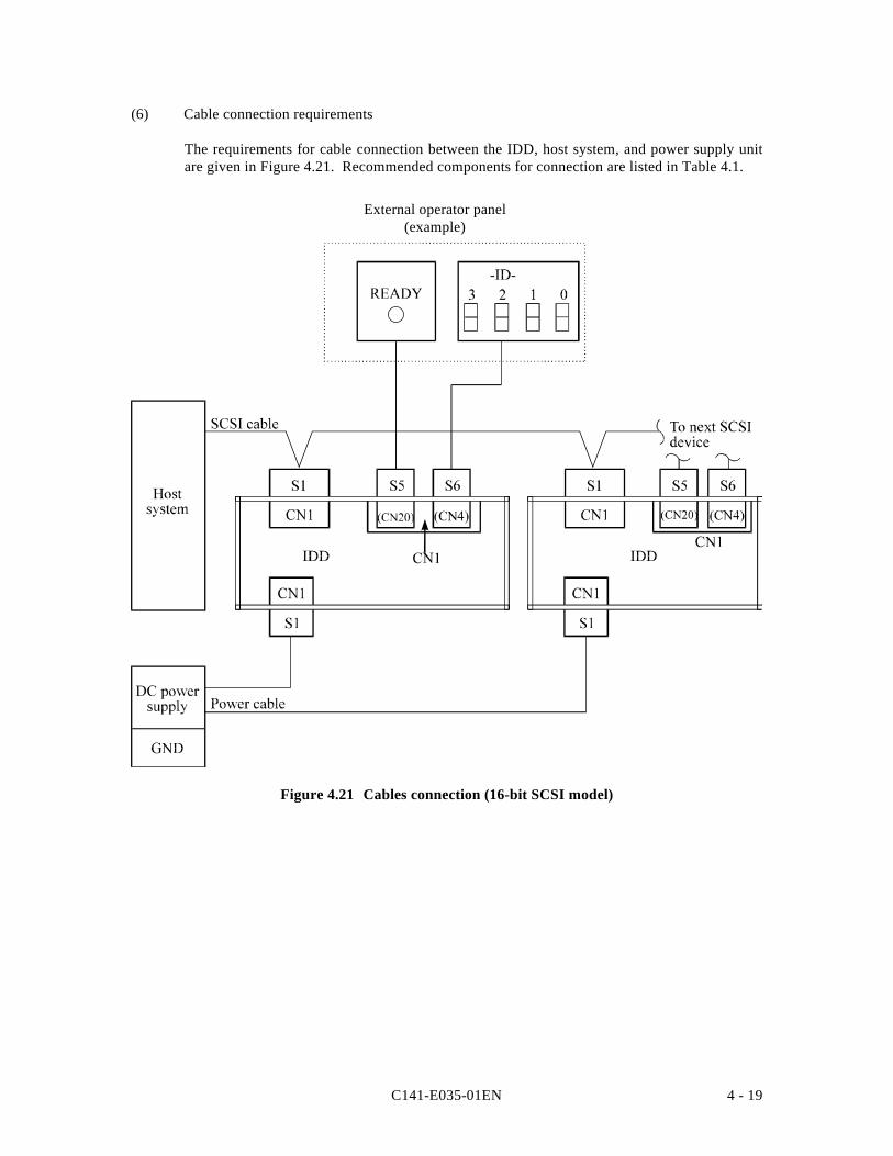
C141-E035-01EN 4 - 19
(6) Cable connection requirements
The requirements for cable connection between the IDD, host system, and power supply unitare given in Figure 4.21. Recommended components for connection are listed in Table 4.1.
Figure 4.21 Cables connection (16-bit SCSI model)
External operator panel(example)
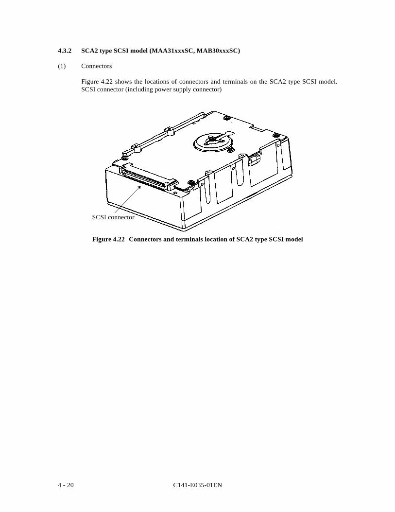
C141-E035-01EN4 - 20
4.3.2 SCA2 type SCSI model (MAA31xxxSC, MAB30xxxSC)
(1) Connectors
Figure 4.22 shows the locations of connectors and terminals on the SCA2 type SCSI model.SCSI connector (including power supply connector)
Figure 4.22 Connectors and terminals location of SCA2 type SCSI model
SCSI connector
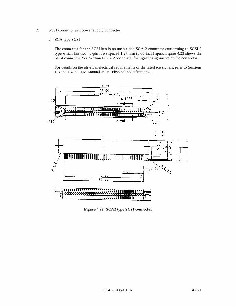
C141-E035-01EN 4 - 21
(2) SCSI connector and power supply connector
a. SCA type SCSI
The connector for the SCSI bus is an unshielded SCA-2 connector conforming to SCSI-3type which has two 40-pin rows spaced 1.27 mm (0.05 inch) apart. Figure 4.23 shows theSCSI connector. See Section C.5 in Appendix C for signal assignments on the connector.
For details on the physical/electrical requirements of the interface signals, refer to Sections1.3 and 1.4 in OEM Manual -SCSI Physical Specifications-.
Figure 4.23 SCA2 type SCSI connector
C141-E035-01EN4 - 22
4.3.3 Cable connector requirements
Table 4.3 lists the recommended components cable connection.
Table 4.3 Recommended components for connection
Applicablemodel
Name Par number Manufacturer Reference(Figures 4.22
and 4.30)
MAx3xxxSP SCSI cable (CN1) Cable socket(closed-end type)
786090-7 AMP S1
Signal cable — —
Power supply cable(CN1)
Cable sockethousing
1-480424-0 AMP S1
Contact 60619-4
Cable 60617-4
External operatorpanel (CN7)
Cable sockethousing
608283302845000 ELCO S5(LED)
Contact 608283051330808(wire: AWG24 to 30)
ELCO
608283351330808(wire: AWG22 to 26)
ELCO
Cable sockethousing
FCN-723J006/2M Fujitsu Limited S6(SCSI ID)
Contact FCN-723J-G/AM Fujitsu Limited
Cable AWG28
External operatorpanel (CN1)
Cable sockethousing
FCN-723J012/2M Fujitsu Limited S1
Contact FCN-723J-G/AM Fujitsu Limited
Cable AWG26 to 34
MAx3xxxSC SCSI connector(CN1)
Connector 787311-1 AMP
(1) SCSI cable
All SCSI devices on one bus are daisy-chained with an SCSI cable. A terminating resistormust be mounted in the SCSI device at each end of the SCSI cable.
Because an SCSI terminating resistor module has been mounted in the IDD of single-endedtype SCSI at factory shipment, it must be set to not-connection when the IDD is not connectedat either end of the SCSI cable. See Section 5.3 for details.
The maximum number of SCSI devices that can be connected to the SCSI bus is 8 for the 8-bitSCSI and 16 for the 16-bit SCSI, including the host adapter, IDD, and other SCSI equipment.
For the 8-bit SCSI, the connector (socket) for the SCSI cable must be an unshielded 50-contactsocket having two 25-contact rows spaced 2.54 mm (0.1 inch) apart. For the 16-bit SCSI, theconnector for the SCSI cable must be an unshielded 68-contact socket having 34-contact rowsspaced 1.27 mm (0.05 inch) apart. (See Figure 4.24.)
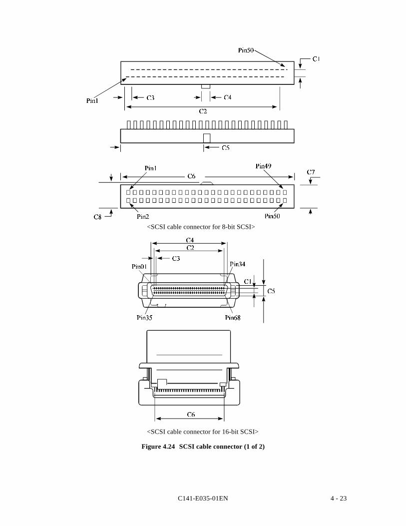
C141-E035-01EN 4 - 23
Figure 4.24 SCSI cable connector (1 of 2)
<SCSI cable connector for 16-bit SCSI>
<SCSI cable connector for 8-bit SCSI>
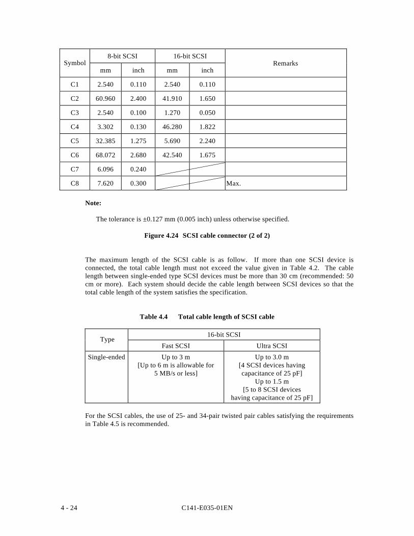
C141-E035-01EN4 - 24
8-bit SCSI 16-bit SCSI
mm inch mm inch
C1 2.540 0.110 2.540 0.110
C2 60.960 2.400 41.910 1.650
C3 2.540 0.100 1.270 0.050
C4 3.302 0.130 46.280 1.822
C5 32.385 1.275 5.690 2.240
C6 68.072 2.680 42.540 1.675
C7 6.096 0.240
C8 7.620 0.300 Max.
Note:
The tolerance is ±0.127 mm (0.005 inch) unless otherwise specified.
Figure 4.24 SCSI cable connector (2 of 2)
The maximum length of the SCSI cable is as follow. If more than one SCSI device isconnected, the total cable length must not exceed the value given in Table 4.2. The cablelength between single-ended type SCSI devices must be more than 30 cm (recommended: 50cm or more). Each system should decide the cable length between SCSI devices so that thetotal cable length of the system satisfies the specification.
Table 4.4 Total cable length of SCSI cable
16-bit SCSI
Fast SCSI Ultra SCSI
Single-ended Up to 3 m[Up to 6 m is allowable for
5 MB/s or less]
Up to 3.0 m[4 SCSI devices havingcapacitance of 25 pF]
Up to 1.5 m[5 to 8 SCSI devices
having capacitance of 25 pF]
For the SCSI cables, the use of 25- and 34-pair twisted pair cables satisfying the requirementsin Table 4.5 is recommended.
Symbol Remarks
Type
C141-E035-01EN 4 - 25
Table 4.5 SCSI cable requirements
Requirements 16-bit SCSI (34-pair)
Conductor size 30 AWG or bigger
Characteristic impedance 90 to 132 Ω
Twist pair cable condition Pins n and n + 33
To maintain the transmission characteristics and reduce signal reflection, cables havingdifferent a characteristic impedance must not be used on the same SCSI bus.
When an SCSI device is connected to the SCSI cable at a point other than either end of thecable, connection to the SCSI connector must be at a branch point of the cable. If an SCSIdevice is connected to last SCSI device except when the cable has a terminating resistor. (SeeFigure 4.25.)
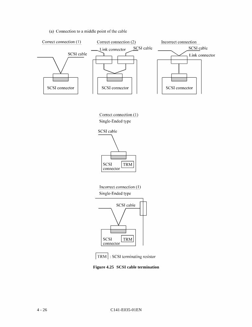
C141-E035-01EN4 - 26
Figure 4.25 SCSI cable termination

C141-E035-01EN 4 - 27
(2) Power cable
IDDs must be star-connected to the DC power supply (one to one connection) to reduce theinfluence of load variations.
(3) DC ground
The DC ground cable must always be connected to the IDD because no fasten terminaldedicated to SG is provided with the IDD. Therefore, when SG and FG are connected in thesystem, it is necessary to connect SG and FG at the power supply or to connect SG of thepower supply to FG of the system.
(4) External operator panel
The external operator panel is installed only when required for the system. When connectionis not required, leave open the following pins in the external operator panel connector of theIDD : Pins 15, 16 and 01 pins 10 through 08 (16 bit-SCSI) in CN7 and pins A1 through A12(16 bit-SCSI) in CN1.
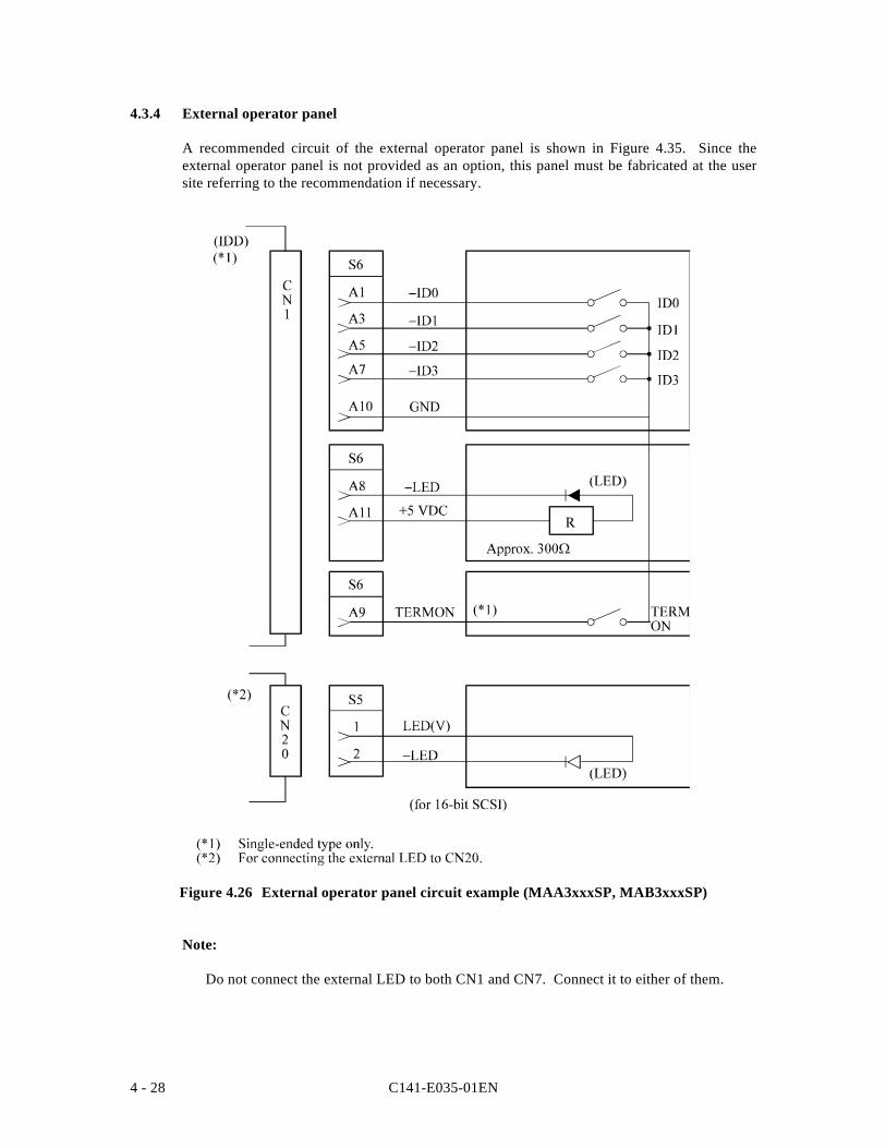
C141-E035-01EN4 - 28
4.3.4 External operator panel
A recommended circuit of the external operator panel is shown in Figure 4.35. Since theexternal operator panel is not provided as an option, this panel must be fabricated at the usersite referring to the recommendation if necessary.
Figure 4.26 External operator panel circuit example (MAA3xxxSP, MAB3xxxSP)
Note:
Do not connect the external LED to both CN1 and CN7. Connect it to either of them.

C141-E035-01EN 5 - 1
CHAPTER 5 INSTALLATION
5.1 Notes on Handling Drives
5.2 Connections
5.3 Setting Terminals
5.4 Mounting Drives
5.5 Connecting Cables
5.6 Confirming Operations after Installation and Preparationfor Use
5.7 Dismounting Drives
This chapter describes the notes on handling drives, connections, setting switches and plugs, mountingdrives, connecting cables, confirming drive operations after installation and preparation for use, anddismounting drives.
5.1 Notes on Handling Drives
(1) General notes
a) Do not give the drive shocks or vibrations exceeding the value defined in the standardbecause it may cause critical damage to the drive. Especially be careful when unpacking.
b) Do not leave the drive in a dirty or contaminated environment.
c) Since static discharge may destroy the CMOS semiconductors in the drive, note thefollowing after unpacking:
• Use an antistatic mat and body grounding when handling the drive.• Hold the DE when handling the drive. Do not touch PCAs except for setting.
(2) Unpackaging
a) Use a flat work area. Check that the "This Side Up" sign side is up. Handle the packageon soft material such as a rubber mat, not on hard material such as a desk.
b) Be careful not to give excess pressure to the internal unit when removing cushions.
c) Be careful not to give excess pressure to the PCAs and interface connector when removingthe drive from the antistatic bag.
d) Do not remove the sealing label or cover of the DE and screws.

C141-E035-01EN5 - 2
(3) Installation
a) Do not attempt to connect or disconnect connections when power is on. The only pinsettings that may be altered are pins 5-6 (Write Protect) in CN6/CN7.
b) Do not move the drive when power is turned on or until the drive completely stops (for 30seconds) after power is turned off.
(4) Packaging
a) Store the drive in an antistatic vinyl bag with a desiccant (silica gel).
b) It is recommended to use the same cushions and packages as those at delivery. If those atdelivery cannot be used, use a package with shock absorption so that the drive is free fromdirect shocks. In this case, fully protect the PCAs and interface connector so that they arenot damaged.
c) Indicate "This Side Up" and "Handle With Care" on the outside of the package so that it isnot turned over.
(5) Delivery
a) When delivering the drive, provide packaging and do not turn it over.
b) Minimize the delivery distance after unpacking and avoid shocks and vibrations withcushions. For the carrying direction at delivery, use one of the mount allowable directionsin Subsection 4.2.2 (vertical direction is recommended).
(6) Storage
a) Provide vaporproof packaging for storage.
b) The storage environment must satisfy the requirements specified in Subsection 2.1.3 whenthe drive is not operating.
c) To prevent condensation, avoid sudden changes in temperature.
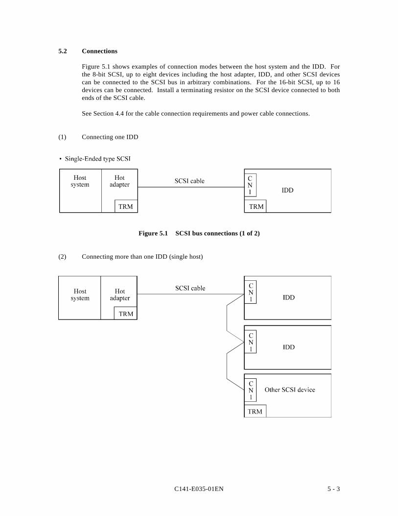
C141-E035-01EN 5 - 3
5.2 Connections
Figure 5.1 shows examples of connection modes between the host system and the IDD. Forthe 8-bit SCSI, up to eight devices including the host adapter, IDD, and other SCSI devicescan be connected to the SCSI bus in arbitrary combinations. For the 16-bit SCSI, up to 16devices can be connected. Install a terminating resistor on the SCSI device connected to bothends of the SCSI cable.
See Section 4.4 for the cable connection requirements and power cable connections.
(1) Connecting one IDD
Figure 5.1 SCSI bus connections (1 of 2)
(2) Connecting more than one IDD (single host)
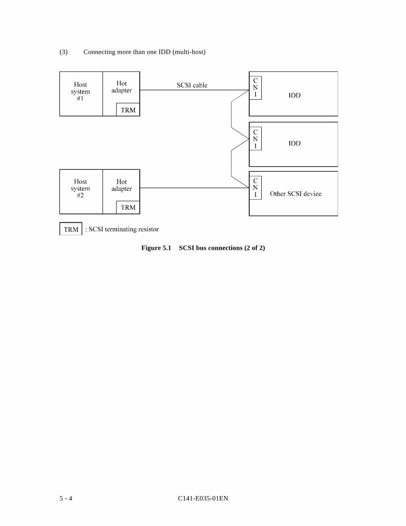
C141-E035-01EN5 - 4
(3) Connecting more than one IDD (multi-host)
Figure 5.1 SCSI bus connections (2 of 2)
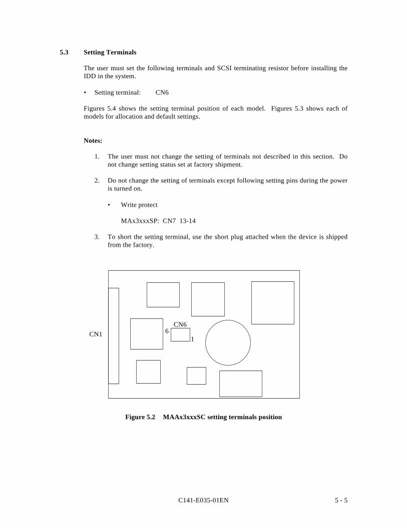
C141-E035-01EN 5 - 5
5.3 Setting Terminals
The user must set the following terminals and SCSI terminating resistor before installing theIDD in the system.
• Setting terminal: CN6
Figures 5.4 shows the setting terminal position of each model. Figures 5.3 shows each ofmodels for allocation and default settings.
Notes:
1. The user must not change the setting of terminals not described in this section. Donot change setting status set at factory shipment.
2. Do not change the setting of terminals except following setting pins during the poweris turned on.
• Write protect
MAx3xxxSP: CN7 13-14
3. To short the setting terminal, use the short plug attached when the device is shippedfrom the factory.
Figure 5.2 MAAx3xxxSC setting terminals position
16
CN6CN1
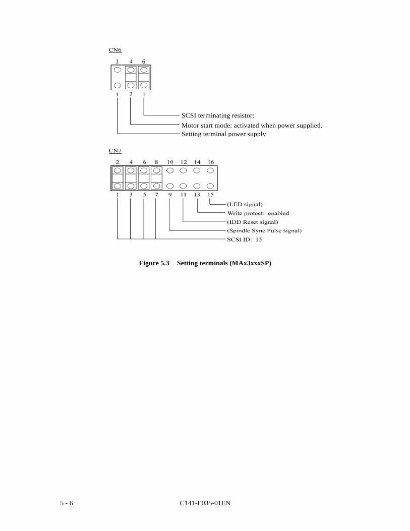
C141-E035-01EN5 - 6
Figure 5.3 Setting terminals (MAx3xxxSP)
Setting terminal power supplyMotor start mode: activated when power supplied.SCSI terminating resistor:connected
11
61
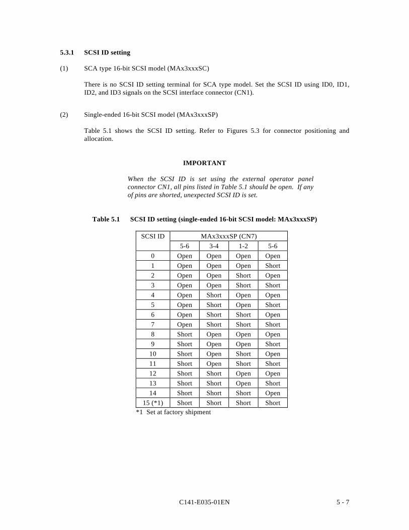
C141-E035-01EN 5 - 7
5.3.1 SCSI ID setting
(1) SCA type 16-bit SCSI model (MAx3xxxSC)
There is no SCSI ID setting terminal for SCA type model. Set the SCSI ID using ID0, ID1,ID2, and ID3 signals on the SCSI interface connector (CN1).
(2) Single-ended 16-bit SCSI model (MAx3xxxSP)
Table 5.1 shows the SCSI ID setting. Refer to Figures 5.3 for connector positioning andallocation.
IMPORTANT
When the SCSI ID is set using the external operator panelconnector CN1, all pins listed in Table 5.1 should be open. If anyof pins are shorted, unexpected SCSI ID is set.
Table 5.1 SCSI ID setting (single-ended 16-bit SCSI model: MAx3xxxSP)
SCSI ID MAx3xxxSP (CN7)5-6 3-4 1-2 5-6
0 Open Open Open Open1 Open Open Open Short2 Open Open Short Open3 Open Open Short Short4 Open Short Open Open5 Open Short Open Short6 Open Short Short Open7 Open Short Short Short8 Short Open Open Open9 Short Open Open Short
10 Short Open Short Open11 Short Open Short Short12 Short Short Open Open13 Short Short Open Short14 Short Short Short Open
15 (*1) Short Short Short Short*1 Set at factory shipment
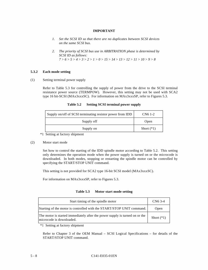
C141-E035-01EN5 - 8
IMPORTANT
1. Set the SCSI ID so that there are no duplicates between SCSI deviceson the same SCSI bus.
2. The priority of SCSI bus use in ARBITRATION phase is determined bySCSI ID as follows:7 > 6 > 5 > 4 > 3 > 2 > 1 > 0 > 15 > 14 > 13 > 12 > 11 > 10 > 9 > 8
5.3.2 Each mode setting
(1) Setting terminal power supply
Refer to Table 5.3 for controlling the supply of power from the drive to the SCSI terminalresistance power source (TERMPOW). However, this setting may not be used with SCA2type 16 bit-SCSI (MAx3xxxSC). For information on MAx3xxxSP, refer to Figures 5.3.
Table 5.2 Setting SCSI terminal power supply
Supply on/off of SCSI terminating resistor power from IDD CN6 1-2
Supply off Open
Supply on Short (*1)
*1 Setting at factory shipment
(2) Motor start mode
Set how to control the starting of the IDD spindle motor according to Table 5.2. This settingonly determines the operation mode when the power supply is turned on or the microcode isdownloaded. In both modes, stopping or restarting the spindle motor can be controlled byspecifying the START/STOP UNIT command.
This setting is not provided for SCA2 type 16-bit SCSI model (MAx3xxxSC).
For information on MAx3xxxSP, refer to Figures 5.3.
Table 5.3 Motor start mode setting
Start timing of the spindle motor CN6 3-4
Starting of the motor is controlled with the START/STOP UNIT command. Open
The motor is started immediately after the power supply is turned on or themicrocode is downloaded. Short (*1)
*1 Setting at factory shipment
Refer to Chapter 3 of the OEM Manual – SCSI Logical Specifications – for details of theSTART/STOP UNIT command.
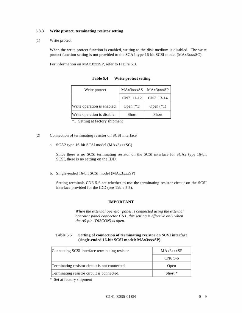
C141-E035-01EN 5 - 9
5.3.3 Write protect, terminating resistor setting
(1) Write protect
When the write protect function is enabled, writing to the disk medium is disabled. The writeprotect function setting is not provided to the SCA2 type 16-bit SCSI model (MAx3xxxSC).
For information on MAx3xxxSP, refer to Figure 5.3.
Table 5.4 Write protect setting
Write protect MAx3xxxSS MAx3xxxSP
CN7 11-12 CN7 13-14
Write operation is enabled. Open (*1) Open (*1)
Write operation is disable. Short Short
*1 Setting at factory shipment
(2) Connection of terminating resistor on SCSI interface
a. SCA2 type 16-bit SCSI model (MAx3xxxSC)
Since there is no SCSI terminating resistor on the SCSI interface for SCA2 type 16-bitSCSI, there is no setting on the IDD.
b. Single-ended 16-bit SCSI model (MAx3xxxSP)
Setting terminals CN6 5-6 set whether to use the terminating resistor circuit on the SCSIinterface provided for the IDD (see Table 5.5).
IMPORTANT
When the external operator panel is connected using the externaloperator panel connector CN1, this setting is effective only whenthe A9 pin (DISCON) is open.
Table 5.5 Setting of connection of terminating resistor on SCSI interface(single-ended 16-bit SCSI model: MAx3xxxSP)
Connecting SCSI interface terminating resistor MAx3xxxSP
CN6 5-6
Terminating resistor circuit is not connected. Open
Terminating resistor circuit is connected. Short *
* Set at factory shipment
C141-E035-01EN5 - 10
5.3.4 Mode settings
In addition to the previously described settings using setting terminals, the IDD is providedwith several mode settings. The mode settings are enabled by specifying the CHANGEDEFINITION command. Table 5.6 lists the mode settings and their settings at factoryshipment.
Refer to Section 3.1.4 of the OEM Manual –SCSI Logical Specifications– for details of thecommand.
Table 5.6 Default mode settings (by CHANGE DEFINITION command)
Mode setting Contents
SCSI level SCSI-2
SYNCHRONOUS DATA TRANSFER REQUEST messagesending
Sent from IDD
UNIT ATTENTION report mode Reported
Reselection retry count Not restricted
WIDE DATA TRANSFER REQUEST message sending Sent from IDD
Reselection time-out delay 250 ms
Spindle motor start delay time 0 sec
C141-E035-01EN 5 - 11
5.4 Mounting Drives
5.4.1 Check before mounting
Reconfirm if the setting terminals are set correctly before mounting the drive in the systemcabinet. For setting terminals location, see Section 5.3.
(1) Single-ended 16-bit SCSI model (MAx3xxxSP)
Reconfirm if the setting terminals are set correctly according to Table 5.7.
Table 5.7 Setting check list (MAx3xxxSP)
No. Setting contents(Check item)
Settingposition Check Remarks
1 Terminal power supply CN6 1 - 2 Short Open
2 Motor start mode CN6 3 - 4 Short Open
3 Connection of terminatingresistor on SCSI interface
CN6 5 - 6 Short Open
No. Setting contents(Check item)
Settingposition Check Remarks
1 SCSI ID CN7 7 - 8 5 - 6 3 - 4 1 - 2
(SCSI ID = __)
2 Write protect CN7 13 - 14 Short Open
5.4.2 Mounting procedures
Since mounting the drive depends on the system cabinet structure, determine the workprocedures considering the requirements specific to each system. The general mountingmethod and items to be checked are shown below.
See Subsection 4.2 for the details of requirements for installing the IDD.
1) With a system to which an external operator panel is mounted, if it is difficult to access theconnector after the drive is mounted on the system cabinet, connect the external operatorpanel cable before mounting the drive.
2) Fix the drive in the system cabinet with four mounting screws as follows:
• The drive has 10 mounting holes (both sides: 3 ×2, bottom: 4). Fix the drive byusing four mounting holes of both sides or the bottom.
Settingterminal
CN6
Settingterminal
CN7

C141-E035-01EN5 - 12
• Use mounting screws whose lengths inside the drive mounting frame are 4 mm or lesswhen the screws are tightened (see Figure 4.5).
• When mounting the drive, be careful not to damage parts on the PCAs.
3) Check that the DE (signal ground) does not touch the system cabinet chassis (frameground). There must be a 2.5 mm or more space between the DE and chassis (see Figure4.5).
C141-E035-01EN 5 - 13
5.5 Connecting Cables
Connect the IDD and system with the following cables. See Section 4.4 for further details ofthe requirements for IDD connector positions and connecting cables.
• Power cable• SCSI cable• External operator panel cable (if required)• Spindle sync cable
The general procedures and notes on connecting cables are described below. Especially, payattention to the inserting direction of each cable connector.
CAUTION
1. Check that system power is off before connecting or disconnectingcables.
2. Do not connect or disconnect cables when power is on.
a) Connect power cable.
b) Connect the external operator panel (if required for system).
c) Connect the SCSI cable.
d) Fix the cables so that they do not touch the DE and PCAs, or so that the smooth flow ofthe cooling air in the system cabinet is assured.
C141-E035-01EN5 - 14
CAUTION
1. Be careful of the insertion directions of the SCSI connectors. With thesystem in which terminating resistor power is supplied via the SCSIcable, if the power is turned on, the overcurrent protection fuse of theterminating resistor power supplier may be blown or the cable may beburnt if overcurrent protection is not provided.
When the recommended parts listed in Table 4.1 are used, insertingthe cables in the wrong direction can be prevented.
2. To connect SCSI devices, be careful of the connection position of thecable. Check that the SCSI device with the terminating resistor is thelast device connected to the cable.
5.6 Confirming Operations after Installation and Preparation for use
5.6.1 Confirming initial operations
This section describes the operation check procedures after power is turned on. Since theinitial operation of the IDD depends on the setting of the motor start mode, check the initialoperation by either of the following procedures.
(1) Initial operation in the case of setting so that motor starts at powering-on
a) When power is turned on, the LED blinks an instant and the IDD executes initial self-diagnosis.
b) If an error is detected in the initial self-diagnosis, the LED on the front panel blinksperiodically.
Remark:
The spindle motor may or may not start rotating in this stage.
c) When the IDD status is idle, the LED on the front panel remains off (when the initiatoraccesses the IDD via the SCSI bus, the LED lights).
(2) Initial operation in the case of setting so that motor starts with START/STOP command
a) When power is turned on, the LED blinks an instant and the IDD executes initial self-diagnosis.
b) If an error is detected in the initial self-diagnosis, the LED on the front panel blinks.
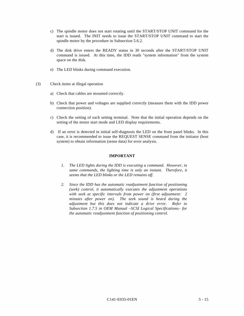
C141-E035-01EN 5 - 15
c) The spindle motor does not start rotating until the START/STOP UNIT command for thestart is issued. The INIT needs to issue the START/STOP UNIT command to start thespindle motor by the procedure in Subsection 5.6.2.
d) The disk drive enters the READY status in 30 seconds after the START/STOP UNITcommand is issued. At this time, the IDD reads "system information" from the systemspace on the disk.
e) The LED blinks during command execution.
(3) Check items at illegal operation
a) Check that cables are mounted correctly.
b) Check that power and voltages are supplied correctly (measure them with the IDD powerconnection position).
c) Check the setting of each setting terminal. Note that the initial operation depends on thesetting of the motor start mode and LED display requirements.
d) If an error is detected in initial self-diagnosis the LED on the front panel blinks. In thiscase, it is recommended to issue the REQUEST SENSE command from the initiator (hostsystem) to obtain information (sense data) for error analysis.
IMPORTANT
1. The LED lights during the IDD is executing a command. However, insame commands, the lighting time is only an instant. Therefore, itseems that the LED blinks or the LED remains off.
2. Since the IDD has the automatic readjustment function of positioning(seek) control, it automatically executes the adjustment operationswith seek at specific intervals from power on (first adjustment: 2minutes after power on). The seek sound is heard during theadjustment but this does not indicate a drive error. Refer toSubsection 1.7.5 in OEM Manual –SCSI Logical Specifications– forthe automatic readjustment function of positioning control.

C141-E035-01EN5 - 16
5.6.2 Checking SCSI connection
When the initial operation is checked normally after power is turned on, check that the IDD isconnected to the SCSI bus from the host system. Although checking the connection dependson the structure of the host system, this section describes the general procedures.
(1) Checking procedure
Issuing the commands and determining the end status depends on the start mode of the spindlemotor and UNIT ATTENTION report mode (specified with setting terminal). Figure 5.7shows the recommended checking procedure for the mode that the motor starts when power isturned on. Figure 5.8 shows for the mode that the motor starts by the START/STOPcommand. In these recommended checking procedures, following items are checked.
Note:
Following steps a) to e) correspond to a) to e) in Figures 5.4 and 5.5.
a) Issue the TEST UNIT READY command and check that the IDD is connectedcorrectly to the SCSI bus and the initial operation after power is turned on endednormally. The command issue period of the TEST UNIT READY command shall bemore than 20 ms.
b) To control starting of the spindle motor from the host system, issue theSTART/STOP UNIT command to start the spindle motor.
c) Check the SCSI bus operations with the WRITE BUFFER and READ BUFFERcommands. Use data whose data bus bits change to 0 or 1 at least once. (Example:Data with an increment pattern of X'00' to X'FF')
d) Read the setting of the terminals with the SEND DIAGNOSTIC and RECEIVEDIAGNOSTIC RESULTS commands and check the setting.
e) Start the IDD self-diagnostic test with the SEND DIAGNOSTIC command and checkthe basic operations of the controller and disk drive.
C141-E035-01EN 5 - 17
Motor starts when power is turned on
Figure 5.4 Checking the SCSI connection (A)

C141-E035-01EN5 - 18
Motor starts by START/STOP command
Figure 5.5 Checking the SCSI connection (B)

C141-E035-01EN 5 - 19
(2) Checking at abnormal end
a) When sense data can be obtained with the REQUEST SENSE command, analyze the sensedata and retry recovery for a recoverable error. Refer to Chapter 4 of OEM Manual – SCSILogical Specifications – for further details.
b) Check the following items for the SCSI cable connection:
• All connectors including other SCSI devices are connected correctly.• The terminating resistor is mounted on both ends of the cable.• Power is connected to the terminating resistor.
c) Check the setting of the terminals. Note that the checking procedure of SCSI connectiondiffers depending on the setting of the motor start mode and UNIT ATTENTION reportmode.
5.6.3 Formatting
Since the disk drive is formatted with a specific (default) data format for each model (partnumber) when shipped from the factory, the disk need not be formatted (initialized) when it isinstalled in the system.
However, when the system needs data attributes different from the default format, all sides ofthe disk must be formatted (initialized) according to the procedures below.
The user can change the following data attributes at initialization:
• Logical data block length• Number of logical data blocks or number of cylinders in the user space• Alternate spare area size
This section outlines the formatting at installation. Refer to Chapters 3 and 5 of OEM Manual– SCSI Logical Specifications – for further details.
(1) MODE SELECT/MODE SELECT EXTENDED command
Specify the format attributes on the disk with the MODE SELECT or MODE SELECTEXTENDED command. The parameters are as follows.
a. Block descriptor
Specify the size (byte length) of the logical data block in the "data block length" field. Toexplicitly specify the number of logical data blocks, specify the number in the "number ofdata blocks" field. Otherwise, specify 0 in "number of data blocks" field. In this case, thenumber of logical data blocks after initialization is determined by the value specified in theformat parameter (page code = 3) and drive parameter (page code = 4).
C141-E035-01EN5 - 20
b. Format parameter (page code = 3)
Specify the number of spare sectors for each cylinder in the "alternate sectors/zone" fieldand specify the number of tracks for alternate cylinders (= number of alternate cylinders ×number of disk drive heads) in the "alternate tracks/zone" field. It is recommended not tospecify values smaller than the IDD default value in this field.
c. Drive parameter (page code = 4)
To explicitly specify the number of cylinders in the user space, specify the number in the"number of cylinders" field. Note that the number of alternate cylinders specified by theformat parameter (page code = 3) is included in the number of cylinders in the user space.When the number of cylinders need not be specified, specify 0 or the default value in the"number of cylinders" field. In this case, either of the smaller value between the numberof cylinders to allocate the number of logical data blocks specified in the "number of datablocks" field of the block descriptor or the maximum number of cylinders that can be usedas the user space on the disk drive is allocated in the user space. When 0 is specified bothin the "number of cylinders" field and the "number of data blocks" field of the blockdescriptor, the maximum number of cylinders that can be used as the user space on thedisk drive is allocated in the user space.
(2) FORMAT UNIT command
Initialize all sides of the disk with the FORMAT UNIT command. The FORMAT UNITcommand initializes all sides of the disk using the P lists, verifies data blocks afterinitialization, and allocates an alternate block for a defect block detected with verification.With initialization, the value specified in the "initializing data pattern" field of the CDB iswritten into all bytes of all logical data blocks. Only the position information of defect blocksdetected with verification is registered in the G list. The specifications are as follows:
a. Specifying CDB
Specify 0 for the "FmtData" bit and the "CmpLst" bit on CDB, 000 for the "Defect ListFormat" field, and data pattern written into the data block at initialization for the"initializing data pattern" field.
b. Format parameter
When the values in step a. are specified with CDB, the format parameter is not needed.
C141-E035-01EN 5 - 21
5.6.4 Setting parameters
The user can specify the optimal operation mode for the user system environments by settingthe following parameters with the MODE SELECT or MODE SELECT EXTENDEDcommand:
• Error recovery parameter• Disconnection/reconnection parameter• Caching parameter• Control mode parameter
With the MODE SELECT or MODE SELECT EXTENDED command, specify 1 for the "SP"bit on CDB to save the specified parameter value on the disk. This enables the IDD to operateby using the parameter value set by the user when power is turned on again. When the systemhas more than one INIT, different parameter value can be set for each INIT.
When the parameters are not set or saved with the MODE SELECT or MODE SELECTEXTENDED command, the IDD sets the default values for parameters and operates whenpower is turned on or after reset. Although the IDD operations are assured with the defaultvalues, the operations are not always optimal for the system. To obtain the best performance,set the parameters in consideration of the system requirements specific to the user.
This section outlines the parameter setting procedures. Refer to Chapter 3 of OEM Manual –SCSI Logical Specifications– for further details of the MODE SELECT and MODE SELECTEXTENDED commands and specifying the parameters.
IMPORTANT
1. At factory shipment of the IDD, the saving operation for the MODESELECT parameter is not executed. So, if the user does not setparameters, the IDD operates according to the default value of eachparameter
2. The MODE SELECT parameter except the number of cache segmentand Queue error management parameter is saved for each SCSI ID ofthe INIT. When the SCSI ID of the INIT needs to be changed forsystem requirements, parameters must be set again. Also in the multi-INIT system, parameters must be set for each INIT.
3. Once parameters are saved, the saved value is effective until nextsaving operation is executed by the INIT having a same SCSI ID. Forexample, even if the initialization of the disk is performed by theFORMAT UNIT command, the saved value of parameters described inthis section is not affected.
4. When the IDD, to which the saving operation has been executed on asystem, is connected to another system, the user must pay attention tothat the IDD operates according to the saved parameter value if thesaving operation is not executed at installation.
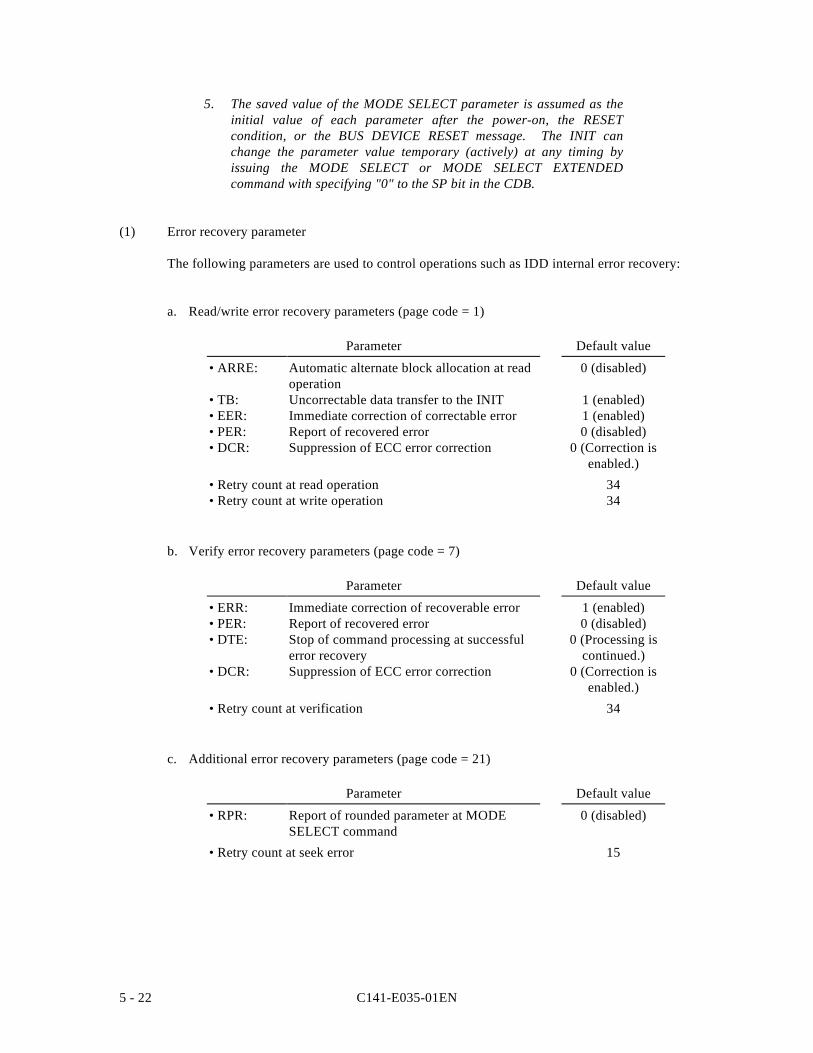
C141-E035-01EN5 - 22
5. The saved value of the MODE SELECT parameter is assumed as theinitial value of each parameter after the power-on, the RESETcondition, or the BUS DEVICE RESET message. The INIT canchange the parameter value temporary (actively) at any timing byissuing the MODE SELECT or MODE SELECT EXTENDEDcommand with specifying "0" to the SP bit in the CDB.
(1) Error recovery parameter
The following parameters are used to control operations such as IDD internal error recovery:
a. Read/write error recovery parameters (page code = 1)
Parameter Default value
• ARRE:
• TB:• EER:• PER:• DCR:
Automatic alternate block allocation at readoperationUncorrectable data transfer to the INITImmediate correction of correctable errorReport of recovered errorSuppression of ECC error correction
0 (disabled)
1 (enabled)1 (enabled)0 (disabled)
0 (Correction isenabled.)
• Retry count at read operation• Retry count at write operation
3434
b. Verify error recovery parameters (page code = 7)
Parameter Default value
• ERR:• PER:• DTE:
• DCR:
Immediate correction of recoverable errorReport of recovered errorStop of command processing at successfulerror recoverySuppression of ECC error correction
1 (enabled)0 (disabled)
0 (Processing iscontinued.)
0 (Correction isenabled.)
• Retry count at verification 34
c. Additional error recovery parameters (page code = 21)
Parameter Default value
• RPR: Report of rounded parameter at MODESELECT command
0 (disabled)
• Retry count at seek error 15

C141-E035-01EN 5 - 23
Notes:
1. The user can arbitrarily specify the following parameters according to the systemrequirements:
• ARRE• TB• PER
2. The user also can arbitrarily specify parameters other than the above. However, it isrecommended to use the default setting in normal operations.
(2) Disconnection/reconnection parameters (page code = 2)
The following parameters are used to optimize the start timing of reconnection processing totransfer data on the SCSI bus at a read (READ or READ EXTENDED command) or writeoperation (WRITE, WRITE EXTENDED, or WRITE AND VERIFY command) of the disk.Refer to Chapter 2 of OEM Manual –SCSI Logical Specifications– for further details.
a. Disconnection/reconnection parameters (page code = 2)
Parameter Default value
• Buffer full ratio 20 (HEX)
• Buffer empty ratio 20 (HEX)
Notes:
1. In a system without the disconnection function, these parameters need not bespecified.
2. Determine the parameter values in consideration of the following performance factorsof the system:
• Time required for reconnection processing• Average data transfer rate of the SCSI bus• Average amount of processing data specified with a command
Refer to Chapter 2 of OEM Manual –SCSI Logical Specifications– for how to obtainthe rough calculation values for the parameter values to be set. It is recommended toevaluate the validity of the specified values by measuring performance in an operationstatus under the average system load requirements.
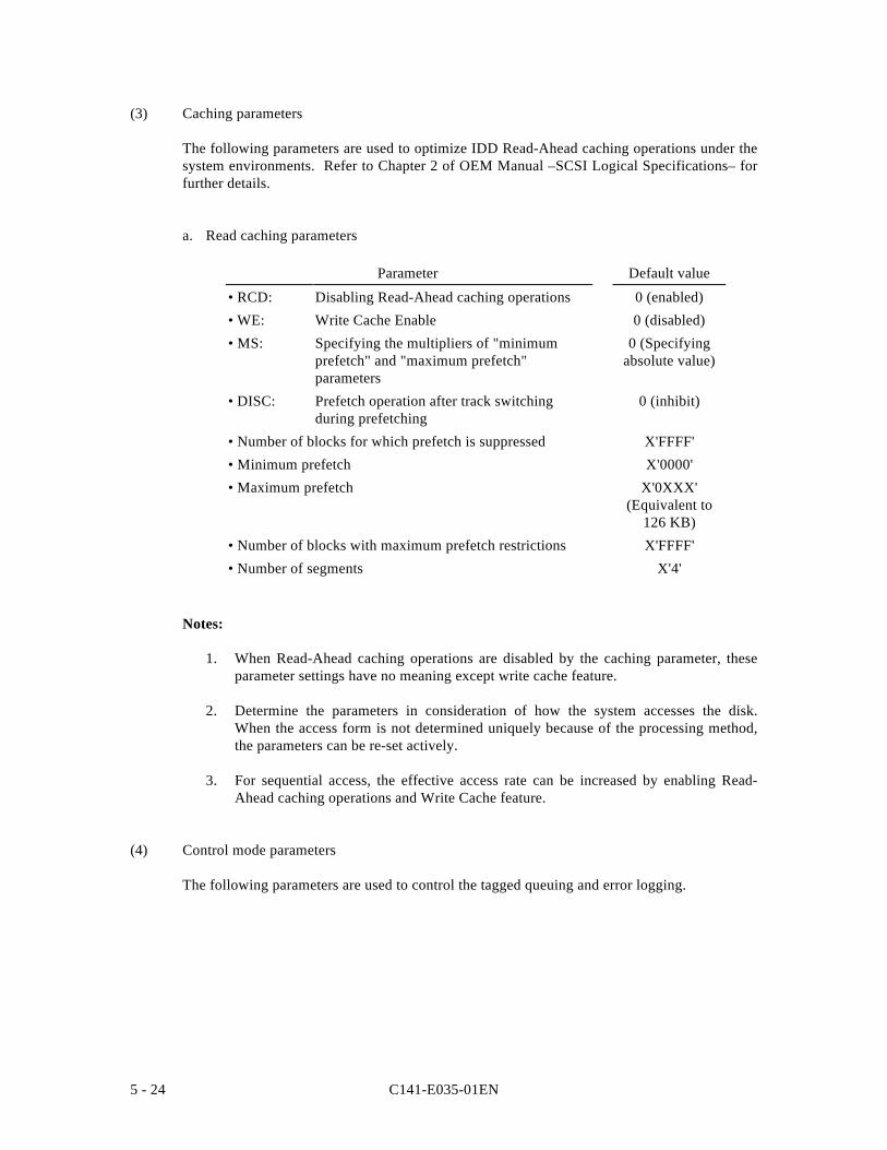
C141-E035-01EN5 - 24
(3) Caching parameters
The following parameters are used to optimize IDD Read-Ahead caching operations under thesystem environments. Refer to Chapter 2 of OEM Manual –SCSI Logical Specifications– forfurther details.
a. Read caching parameters
Parameter Default value
• RCD: Disabling Read-Ahead caching operations 0 (enabled)
• WE: Write Cache Enable 0 (disabled)
• MS: Specifying the multipliers of "minimumprefetch" and "maximum prefetch"parameters
0 (Specifyingabsolute value)
• DISC: Prefetch operation after track switchingduring prefetching
0 (inhibit)
• Number of blocks for which prefetch is suppressed X'FFFF'
• Minimum prefetch X'0000'
• Maximum prefetch X'0XXX'(Equivalent to
126 KB)
• Number of blocks with maximum prefetch restrictions X'FFFF'
• Number of segments X'4'
Notes:
1. When Read-Ahead caching operations are disabled by the caching parameter, theseparameter settings have no meaning except write cache feature.
2. Determine the parameters in consideration of how the system accesses the disk.When the access form is not determined uniquely because of the processing method,the parameters can be re-set actively.
3. For sequential access, the effective access rate can be increased by enabling Read-Ahead caching operations and Write Cache feature.
(4) Control mode parameters
The following parameters are used to control the tagged queuing and error logging.
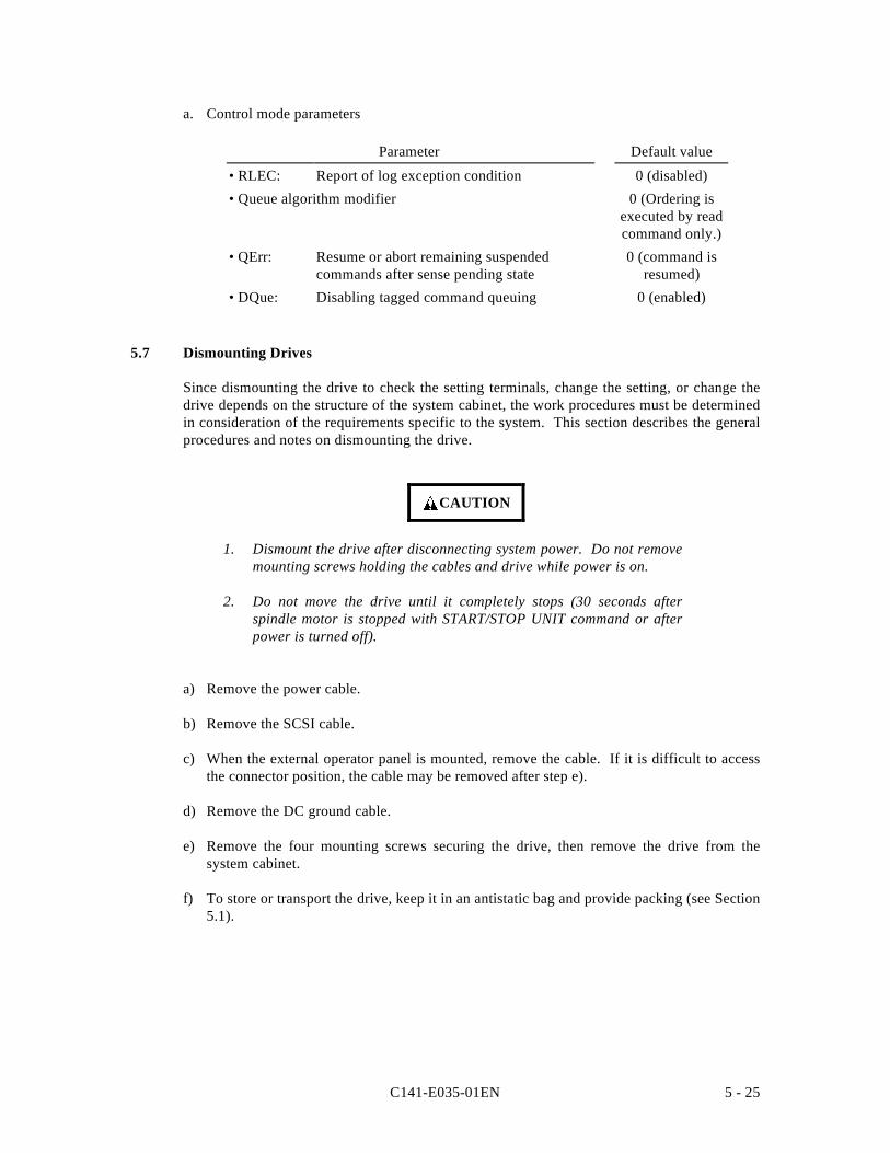
C141-E035-01EN 5 - 25
a. Control mode parameters
Parameter Default value
• RLEC: Report of log exception condition 0 (disabled)
• Queue algorithm modifier 0 (Ordering isexecuted by readcommand only.)
• QErr: Resume or abort remaining suspendedcommands after sense pending state
0 (command isresumed)
• DQue: Disabling tagged command queuing 0 (enabled)
5.7 Dismounting Drives
Since dismounting the drive to check the setting terminals, change the setting, or change thedrive depends on the structure of the system cabinet, the work procedures must be determinedin consideration of the requirements specific to the system. This section describes the generalprocedures and notes on dismounting the drive.
CAUTION
1. Dismount the drive after disconnecting system power. Do not removemounting screws holding the cables and drive while power is on.
2. Do not move the drive until it completely stops (30 seconds afterspindle motor is stopped with START/STOP UNIT command or afterpower is turned off).
a) Remove the power cable.
b) Remove the SCSI cable.
c) When the external operator panel is mounted, remove the cable. If it is difficult to accessthe connector position, the cable may be removed after step e).
d) Remove the DC ground cable.
e) Remove the four mounting screws securing the drive, then remove the drive from thesystem cabinet.
f) To store or transport the drive, keep it in an antistatic bag and provide packing (see Section5.1).

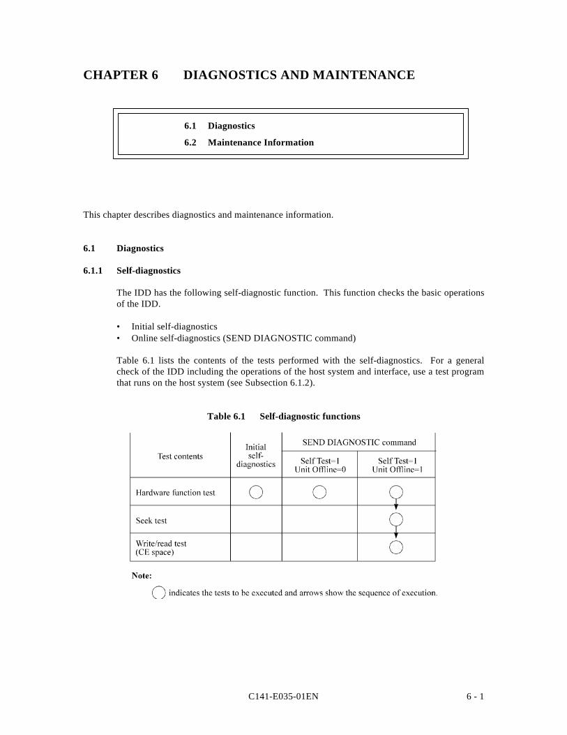
C141-E035-01EN 6 - 1
CHAPTER 6 DIAGNOSTICS AND MAINTENANCE
6.1 Diagnostics
6.2 Maintenance Information
This chapter describes diagnostics and maintenance information.
6.1 Diagnostics
6.1.1 Self-diagnostics
The IDD has the following self-diagnostic function. This function checks the basic operationsof the IDD.
• Initial self-diagnostics• Online self-diagnostics (SEND DIAGNOSTIC command)
Table 6.1 lists the contents of the tests performed with the self-diagnostics. For a generalcheck of the IDD including the operations of the host system and interface, use a test programthat runs on the host system (see Subsection 6.1.2).
Table 6.1 Self-diagnostic functions

C141-E035-01EN6 - 2
Brief test contents of self-diagnostics are as follows.
a. Hardware function test
This test checks the basic operation of the controller section, and contains following test.
• RAM (microcode is stored)• Peripheral circuits of microprocessor (MPU)• Memory (RAM)• Data buffer
b. Seek test
This test checks the positioning operation of the disk drive using several seek modes (2points seek, 1 position sequential seek, etc.). The positioning operation is checked withconfirming the physical address information by reading the ID field from the data block ontrack 0 after completion of the seek operation to the target cylinder.
c. Write/read test
This test check the write/read function by using the Internal test space of the disk drive.
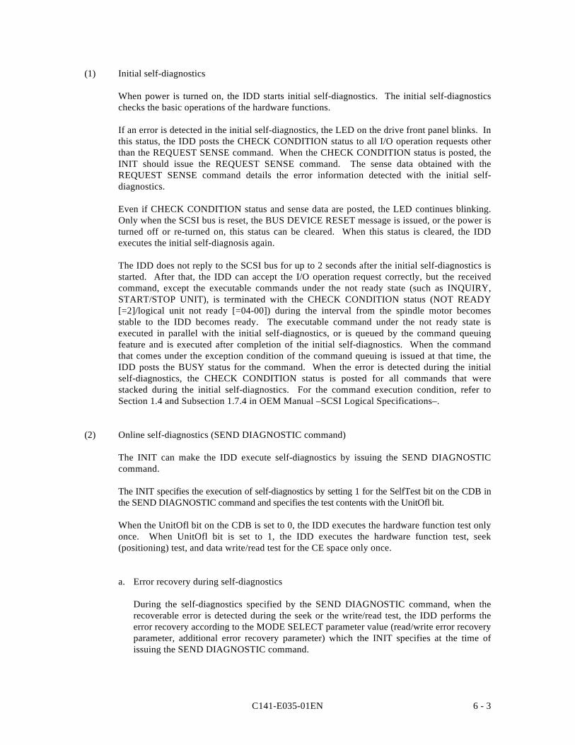
C141-E035-01EN 6 - 3
(1) Initial self-diagnostics
When power is turned on, the IDD starts initial self-diagnostics. The initial self-diagnosticschecks the basic operations of the hardware functions.
If an error is detected in the initial self-diagnostics, the LED on the drive front panel blinks. Inthis status, the IDD posts the CHECK CONDITION status to all I/O operation requests otherthan the REQUEST SENSE command. When the CHECK CONDITION status is posted, theINIT should issue the REQUEST SENSE command. The sense data obtained with theREQUEST SENSE command details the error information detected with the initial self-diagnostics.
Even if CHECK CONDITION status and sense data are posted, the LED continues blinking.Only when the SCSI bus is reset, the BUS DEVICE RESET message is issued, or the power isturned off or re-turned on, this status can be cleared. When this status is cleared, the IDDexecutes the initial self-diagnosis again.
The IDD does not reply to the SCSI bus for up to 2 seconds after the initial self-diagnostics isstarted. After that, the IDD can accept the I/O operation request correctly, but the receivedcommand, except the executable commands under the not ready state (such as INQUIRY,START/STOP UNIT), is terminated with the CHECK CONDITION status (NOT READY[=2]/logical unit not ready [=04-00]) during the interval from the spindle motor becomesstable to the IDD becomes ready. The executable command under the not ready state isexecuted in parallel with the initial self-diagnostics, or is queued by the command queuingfeature and is executed after completion of the initial self-diagnostics. When the commandthat comes under the exception condition of the command queuing is issued at that time, theIDD posts the BUSY status for the command. When the error is detected during the initialself-diagnostics, the CHECK CONDITION status is posted for all commands that werestacked during the initial self-diagnostics. For the command execution condition, refer toSection 1.4 and Subsection 1.7.4 in OEM Manual –SCSI Logical Specifications–.
(2) Online self-diagnostics (SEND DIAGNOSTIC command)
The INIT can make the IDD execute self-diagnostics by issuing the SEND DIAGNOSTICcommand.
The INIT specifies the execution of self-diagnostics by setting 1 for the SelfTest bit on the CDB inthe SEND DIAGNOSTIC command and specifies the test contents with the UnitOfl bit.
When the UnitOfl bit on the CDB is set to 0, the IDD executes the hardware function test onlyonce. When UnitOfl bit is set to 1, the IDD executes the hardware function test, seek(positioning) test, and data write/read test for the CE space only once.
a. Error recovery during self-diagnostics
During the self-diagnostics specified by the SEND DIAGNOSTIC command, when therecoverable error is detected during the seek or the write/read test, the IDD performs theerror recovery according to the MODE SELECT parameter value (read/write error recoveryparameter, additional error recovery parameter) which the INIT specifies at the time ofissuing the SEND DIAGNOSTIC command.
C141-E035-01EN6 - 4
PER DTE Operation of self-diagnostics
0 0 The self-diagnostics continues when the error isrecovered. The self-diagnostics terminatesnormally so far as the unrecoverable error is notdetected.
0 1 - - - - (Unspecificable) - - - -
1 0 The self-diagnostics continues when the error isrecovered. If the unrecoverable error is notdetected, the consecutive tests are executed till lasttest but the self-diagnostics terminates with error.The error information indicates that of the lastrecovered error.
1 1 After the error recovery permitted by the parametercompletes, the self-diagnostics stops at the timeeven if the error is recovered. The self-diagnosticswith error and the error information indicates thatof the detected error.
b. Reporting result of self-diagnostics and error indication
When all specified self-diagnostics terminate normally, the IDD posts the GOOD status forthe SEND DIAGNOSTIC command.
When an error is detected in the self-diagnostics, the IDD terminates the SENDDIAGNOSTIC command with the CHECK CONDITION status. At this time only whenan error is detected in the hardware function test, the LED on the front panel of the diskdrive blinks.
The INIT should issue the REQUEST SENSE command when the CHECK CONDITIONstatus is posted. The sense data collected by the REQUEST SENSE command indicatesthe detail information of the error detected in the self-diagnostics.
The IDD status after the CHECK CONDITION status is posted differs according to thetype of the detected error.
a) When an error is detected in the seek or write/read test, the subsequent command canbe accepted correctly. When the command other than the REQUEST SENSE and NOOPERATION is issued from the same INIT, the error information (sense data) iscleared.
b) When an error is detected in the hardware function test, the IDD posts the CHECKCONDITION status for all I/O operation request except the REQUEST SENSEcommand. The error status is not cleared and the LED on the front panel continuesblinking even if the error information (sense data) is read. Only when the SCSI bus isreset, the BUS DEVICE RESET message is issued or the power is turned off or re-turned on, the status can be cleared. When this status is cleared, the IDD executes theinitial self-diagnostics again (see item (1)).
C141-E035-01EN 6 - 5
Refer to Chapter 3 of OEM Manual –SCSI Logical Specifications– for further details ofthe command specifications.
Notes:
When the SEND DIAGNOSTIC command terminates with the CHECK CONDITIONstatus, the INIT must collect the error information using the REQUEST SENSE command.The RECEIVE DIAGNOSTIC RESULTS command cannot read out the error informationdetected in the self-diagnostics.
6.1.2 Test programs
The basic operations of the IDD itself can be checked with the self-diagnostic function.However, to check general operations such as the host system and interface operations in astatus similar to the normal operation status, a test program that runs on the host system mustbe used.
The structure and functions of the test program depend on the user system requirements.Generally, it is recommended to provide a general input/output test program that includesSCSI devices connected to the SCSI bus and input/output devices on other I/O ports.
Including the following test items in the test program is recommended to test the IDDfunctions generally.
(1) Interface (SCSI bus) test
The operations of the SCSI bus and data buffer on the IDD are checked with the WRITEBUFFER and READ BUFFER commands.
(2) Basic operation test
The basic operations of the IDD are checked by executing self-diagnosis with the SENDDIAGNOSTIC command (see Subsection 6.1.1).
(3) Random/sequential read test
The positioning (seek) operation and read operation are tested in random access and sequentialaccess modes with the READ, READ EXTENDED, or VERIFY command.
(4) Write/read test
By using a data block in the CE space, the write/read test can be executed with an arbitrarypattern for a disk drive in which user data is stored.
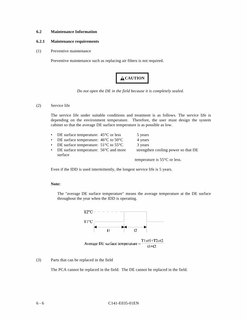
C141-E035-01EN6 - 6
6.2 Maintenance Information
6.2.1 Maintenance requirements
(1) Preventive maintenance
Preventive maintenance such as replacing air filters is not required.
CAUTION
Do not open the DE in the field because it is completely sealed.
(2) Service life
The service life under suitable conditions and treatment is as follows. The service life isdepending on the environment temperature. Therefore, the user must design the systemcabinet so that the average DE surface temperature is as possible as low.
• DE surface temperature: 45°C or less 5 years• DE surface temperature: 46°C to 50°C 4 years• DE surface temperature: 51°C to 55°C 3 years• DE surface temperature: 56°C and more strengthen cooling power so that DE
surfacetemperature is 55°C or less.
Even if the IDD is used intermittently, the longest service life is 5 years.
Note:
The "average DE surface temperature" means the average temperature at the DE surfacethroughout the year when the IDD is operating.
(3) Parts that can be replaced in the field
The PCA cannot be replaced in the field. The DE cannot be replaced in the field.
C141-E035-01EN 6 - 7
(4) Service system and repairs
Fujitsu has the service system and repair facility for the disk drive. Contact Fujitsurepresentative to submit information for replacing or repairing the disk drive. Generally, thefollowing information must be included:
a) IDD model, part number (P/N), revision number, serial number (S/N), and date ofmanufacturing
b) Error status
• Date when the error occurred• System configuration• Environmental conditions (temperature, humidity, and voltage)
c) Error history
d) Error contents
• Outline of inconvenience• Issued commands and specified parameters• Sense data• Other error analysis information
CAUTION
Save data stored on the disk drive before requesting repair.Fujitsu does not assume responsibility if data is destroyed duringservicing or repair.
See Section 5.1 for notes on packing and handling when returning the disk drive.
C141-E035-01EN6 - 8
6.2.2 Revision numbers
The revision number of the disk drive is represented with a letter and a number indicated onthe revision label attached to the DE. Figure 6.1 shows the revision label format.
Figure 6.1 Revision label
(1) Indicating revision number at factory shipment
When the disk drive is shipped from the factory, the revision number is indicated by deletingnumbers in the corresponding letter line up to the corresponding number with = (see Figure6.2).
(2) Changing revision number in the field
To change the revision number because parts are replaced or other modification is applied inthe field, the new level is indicated by enclosing the corresponding number in thecorresponding letter line with (see Figure 6.2).
Note:
When the revision number is changed after the drive is shipped from the factory, Fujitsuissues "Engineering Change Request/Notice" in which the new revision number isindicated. When the user changes the revision number, the user should update the revisionlabel as described in item (2) after applying the modification.
Machine revision
C141-E035-01EN 6 - 9
At shipment
Figure 6.2 Indicating revision numbers
Rev. A3
Rev. A2
Revising at field

C141-E035-01EN A - 1
APPENDIX A LOCATIONS OF CONNECTORS,SETTING TERMINALS, ANDTERMINATING RESISTORS
A.1 Locations of Connectors and Setting Terminals(MAx3xxSC, SCA type 16-bit SCSI)
A.2 Locations of Connectors, Setting Terminals, and(MAx3xxSP : full height, single-ended type 16-bit SCSI)
This appendix shows the locations of connectors, setting terminals, and terminating resistor for 8- and16-bit SCSIs.
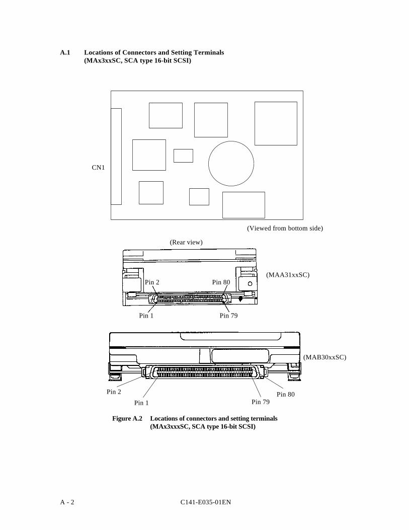
A - 2 C141-E035-01EN
A.1 Locations of Connectors and Setting Terminals(MAx3xxSC, SCA type 16-bit SCSI)
Figure A.2 Locations of connectors and setting terminals(MAx3xxxSC, SCA type 16-bit SCSI)
(MAB30xxSC)
(MAA31xxSC)
(Rear view)
(Viewed from bottom side)
Pin 79
Pin 80
Pin 1
Pin 2
CN1
Pin 80Pin 79
Pin 2
Pin 1
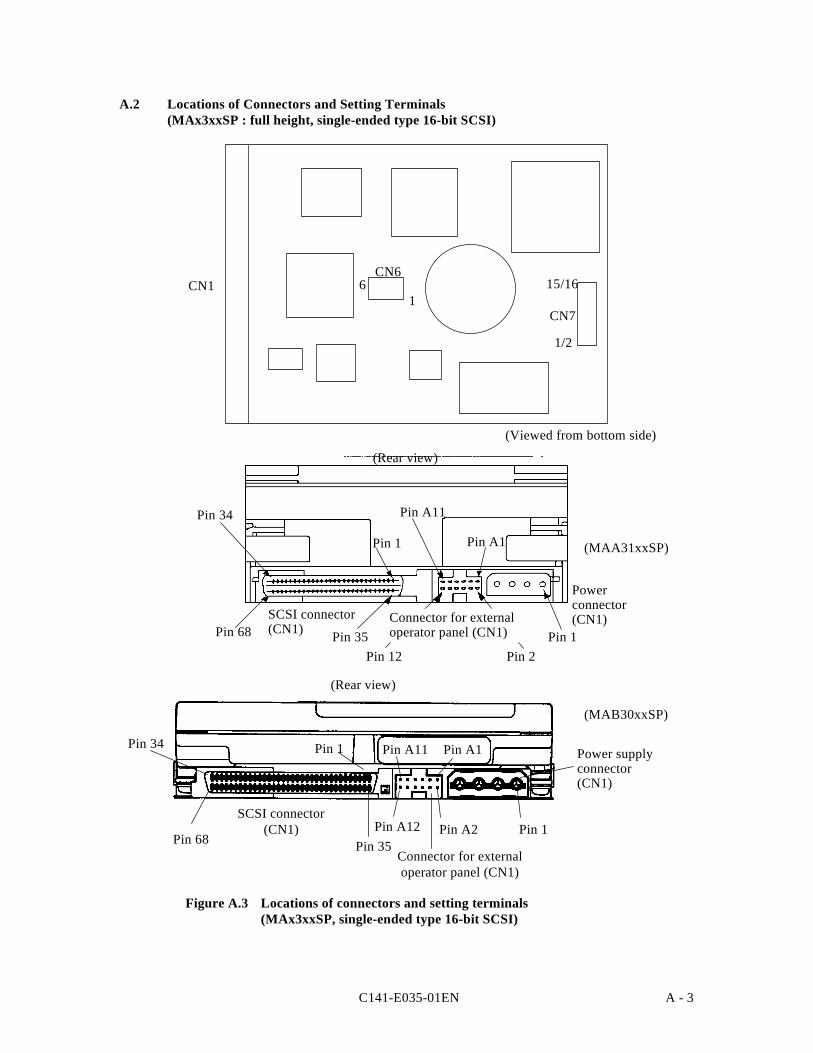
C141-E035-01EN A - 3
A.2 Locations of Connectors and Setting Terminals(MAx3xxSP : full height, single-ended type 16-bit SCSI)
Figure A.3 Locations of connectors and setting terminals(MAx3xxSP, single-ended type 16-bit SCSI)
(Viewed from bottom side)
(MAB30xxSP)
(MAA31xxSP)
(Rear view)
Connector for externaloperator panel (CN1)
Powerconnector(CN1)SCSI connector
(CN1)
Pin 2Pin 12
Pin A1
Pin A11
Pin 1
Pin 1Pin 35
Pin 34
Pin 68
16
1/2
15/16
CN7
CN1CN6
(Rear view)
Pin A1Pin A11Pin 1
Connector for externaloperator panel (CN1)
Power supplyconnector(CN1)
SCSI connector(CN1)
Pin 68
Pin 34
Pin A2Pin A12Pin 35
Pin 1


C141-E035-01EN B - 1
APPENDIX B SETTING TERMINALS
B.1 Setting Terminals(MAx3xxxSP : Single-ended 16-bit SCSI)
This appendix describes setting terminals.
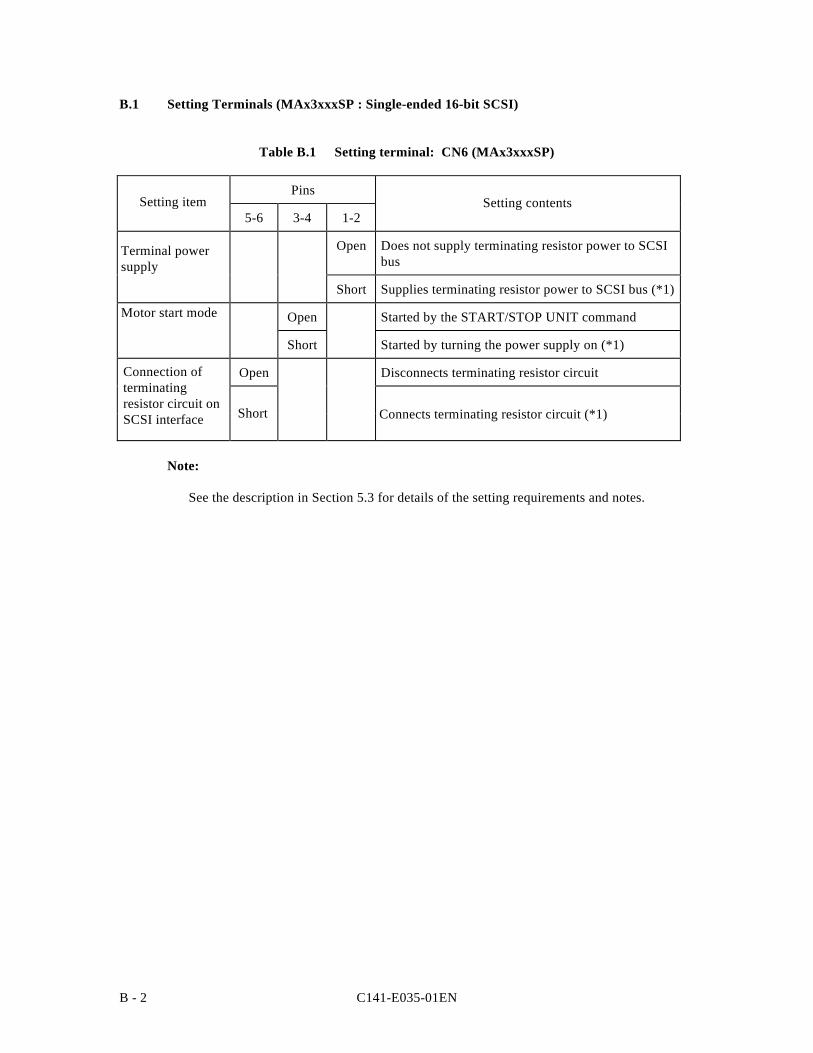
C141-E035-01ENB - 2
B.1 Setting Terminals (MAx3xxxSP : Single-ended 16-bit SCSI)
Table B.1 Setting terminal: CN6 (MAx3xxxSP)
Pins
5-6 3-4 1-2
Open Does not supply terminating resistor power to SCSIbus
Short Supplies terminating resistor power to SCSI bus (*1)
Open Started by the START/STOP UNIT command
Short Started by turning the power supply on (*1)
Open Disconnects terminating resistor circuit
Note:
See the description in Section 5.3 for details of the setting requirements and notes.
Connection ofterminatingresistor circuit onSCSI interface
Motor start mode
Terminal powersupply
Setting item Setting contents
Short Connects terminating resistor circuit (*1)
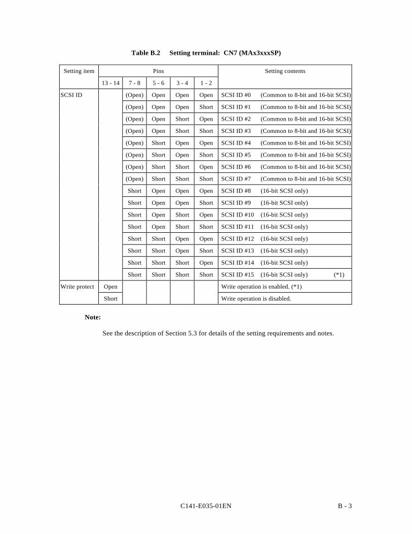
C141-E035-01EN B - 3
Table B.2 Setting terminal: CN7 (MAx3xxxSP)
Setting item Pins Setting contents
13 - 14 7 - 8 5 - 6 3 - 4 1 - 2
SCSI ID (Open) Open Open Open SCSI ID #0 (Common to 8-bit and 16-bit SCSI)
(Open) Open Open Short SCSI ID #1 (Common to 8-bit and 16-bit SCSI)
(Open) Open Short Open SCSI ID #2 (Common to 8-bit and 16-bit SCSI)
(Open) Open Short Short SCSI ID #3 (Common to 8-bit and 16-bit SCSI)
(Open) Short Open Open SCSI ID #4 (Common to 8-bit and 16-bit SCSI)
(Open) Short Open Short SCSI ID #5 (Common to 8-bit and 16-bit SCSI)
(Open) Short Short Open SCSI ID #6 (Common to 8-bit and 16-bit SCSI)
(Open) Short Short Short SCSI ID #7 (Common to 8-bit and 16-bit SCSI)
Short Open Open Open SCSI ID #8 (16-bit SCSI only)
Short Open Open Short SCSI ID #9 (16-bit SCSI only)
Short Open Short Open SCSI ID #10 (16-bit SCSI only)
Short Open Short Short SCSI ID #11 (16-bit SCSI only)
Short Short Open Open SCSI ID #12 (16-bit SCSI only)
Short Short Open Short SCSI ID #13 (16-bit SCSI only)
Short Short Short Open SCSI ID #14 (16-bit SCSI only)
Short Short Short Short SCSI ID #15 (16-bit SCSI only) (*1)
Write protect Open Write operation is enabled. (*1)
Short Write operation is disabled.
Note:
See the description of Section 5.3 for details of the setting requirements and notes.

C141-E035-01EN C - 1
APPENDIX C CONNECTOR SIGNAL ALLOCATION
C.1 SCSI Connector Signal Allocation: SCA type 16-bit SCSI
C.2 SCSI Connector Signal Allocation: single-ended type16-bit SCSI
This appendix describes the connector signal allocation.
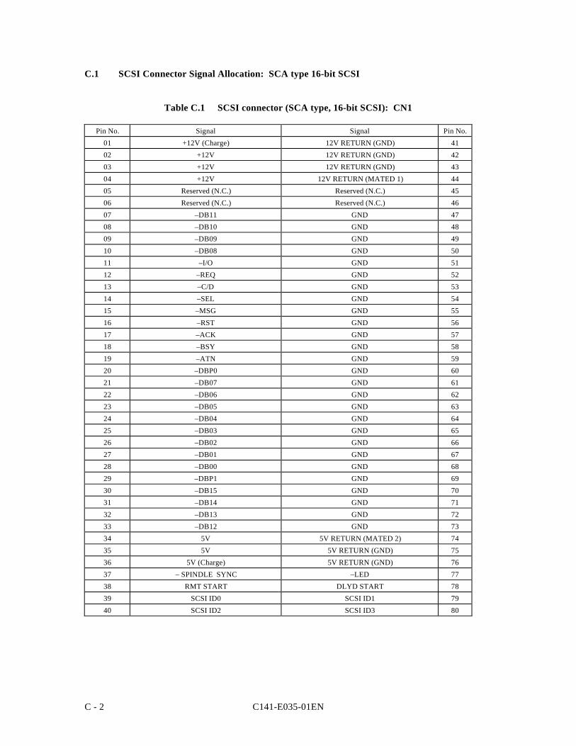
C141-E035-01ENC - 2
C.1 SCSI Connector Signal Allocation: SCA type 16-bit SCSI
Table C.1 SCSI connector (SCA type, 16-bit SCSI): CN1
Pin No. Signal Signal Pin No.
01 +12V (Charge) 12V RETURN (GND) 41
02 +12V 12V RETURN (GND) 42
03 +12V 12V RETURN (GND) 43
04 +12V 12V RETURN (MATED 1) 44
05 Reserved (N.C.) Reserved (N.C.) 45
06 Reserved (N.C.) Reserved (N.C.) 46
07 –DB11 GND 47
08 –DB10 GND 48
09 –DB09 GND 49
10 –DB08 GND 50
11 –I/O GND 51
12 –REQ GND 52
13 –C/D GND 53
14 –SEL GND 54
15 –MSG GND 55
16 –RST GND 56
17 –ACK GND 57
18 –BSY GND 58
19 –ATN GND 59
20 –DBP0 GND 60
21 –DB07 GND 61
22 –DB06 GND 62
23 –DB05 GND 63
24 –DB04 GND 64
25 –DB03 GND 65
26 –DB02 GND 66
27 –DB01 GND 67
28 –DB00 GND 68
29 –DBP1 GND 69
30 –DB15 GND 70
31 –DB14 GND 71
32 –DB13 GND 72
33 –DB12 GND 73
34 5V 5V RETURN (MATED 2) 74
35 5V 5V RETURN (GND) 75
36 5V (Charge) 5V RETURN (GND) 76
37 – SPINDLE SYNC –LED 77
38 RMT START DLYD START 78
39 SCSI ID0 SCSI ID1 79
40 SCSI ID2 SCSI ID3 80
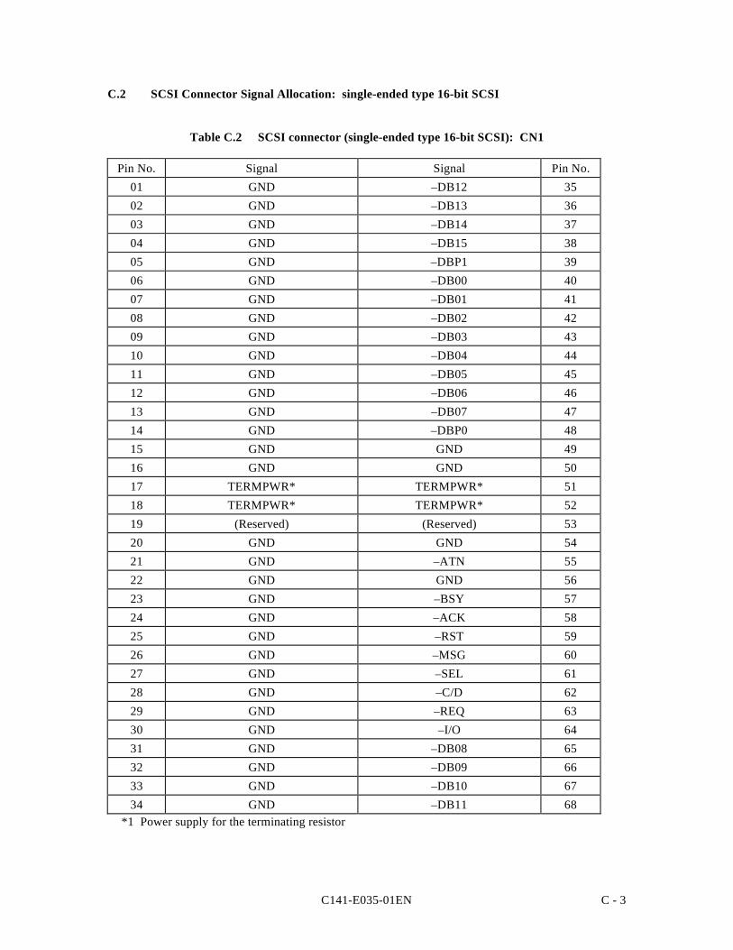
C141-E035-01EN C - 3
C.2 SCSI Connector Signal Allocation: single-ended type 16-bit SCSI
Table C.2 SCSI connector (single-ended type 16-bit SCSI): CN1
Pin No. Signal Signal Pin No.01 GND –DB12 3502 GND –DB13 3603 GND –DB14 3704 GND –DB15 3805 GND –DBP1 3906 GND –DB00 4007 GND –DB01 4108 GND –DB02 4209 GND –DB03 4310 GND –DB04 4411 GND –DB05 4512 GND –DB06 4613 GND –DB07 4714 GND –DBP0 4815 GND GND 4916 GND GND 5017 TERMPWR* TERMPWR* 5118 TERMPWR* TERMPWR* 5219 (Reserved) (Reserved) 5320 GND GND 5421 GND –ATN 5522 GND GND 5623 GND –BSY 5724 GND –ACK 5825 GND –RST 5926 GND –MSG 6027 GND –SEL 6128 GND –C/D 6229 GND –REQ 6330 GND –I/O 6431 GND –DB08 6532 GND –DB09 6633 GND –DB10 6734 GND –DB11 68
*1 Power supply for the terminating resistor


C141-E035-01EN D - 1
APPENDIX D MODEL NAMES AND PRODUCT NUMBERS
D.1 Model Names and Product Numbers
This appendix lists model names (types) and product numbers.
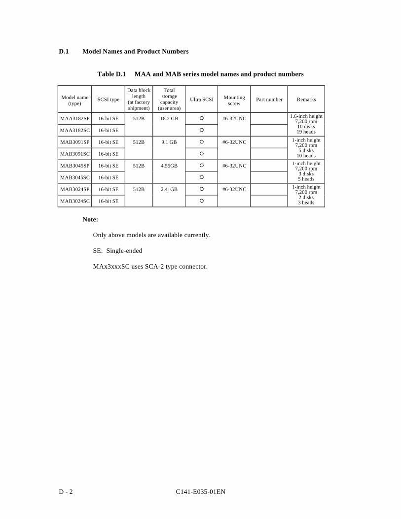
C141-E035-01END - 2
D.1 Model Names and Product Numbers
Table D.1 MAA and MAB series model names and product numbers
Model name(type)
SCSI type
Data blocklength
(at factoryshipment)
Totalstoragecapacity
(user area)
Ultra SCSI Mountingscrew
Part number Remarks
MAA3182SP 16-bit SE 512B 18.2 GB #6-32UNC
MAA3182SC 16-bit SE
MAB3091SP 16-bit SE 512B 9.1 GB #6-32UNC
MAB3091SC 16-bit SE
MAB3045SP 16-bit SE 512B 4.55GB #6-32UNC
MAB3045SC 16-bit SE
MAB3024SP 16-bit SE 512B 2.41GB #6-32UNC
MAB3024SC 16-bit SE
Note:
Only above models are available currently.
SE: Single-ended
MAx3xxxSC uses SCA-2 type connector.
1-inch height7,200 rpm
2 disks3 heads
1-inch height7,200 rpm
3 disks5 heads
1-inch height7,200 rpm
5 disks10 heads
1.6-inch height7,200 rpm10 disks19 heads

C141-E035-01EN E - 1
APPENDIX E SCSI INTERFACE FUNCTIONS
This appendix lists the SCSI interface functions provided for the IDD. Refer to the OEM Manual –SCSI Logical Specifications – for details of each functions.

C141-E035-01ENE - 2
Table E.1 SCSI interface function specifications (1 of 9)
: Provided ×: Not providedItem Specification
COMMAND COMPLETE (00) ΟSAVE DATA POINTER (02) ΟRESTORE POINTERS (03) Ο
(TARG → INIT) (04) Ο
(INIT → TARG) (04) ×INITIATOR DETECTED ERROR (05) ΟABORT (06) ΟMESSAGE REJECT (07) ΟNO OPERATION (08) ×MESSAGE PARITY ERROR (09) ΟLINKED COMMAND COMPLETE (0A) ΟLINKED COMMAND COMPLETE WITH FLAG (0B) ΟBUS DEVICE RESET (0C) ΟABORT TAG (0D) ΟCLEAR QUEUE (0E) ΟINITIATE RECOVERY (0F) ×RELEASE RECOVERY (10) ×TERMINATE I/O PROCESS (11) ΟCONTINUE I/O PROCESS (12) ΟTARGET TRANSFER DISABLE (13) ΟIDENTIFY (80-FF) Ο
Disconnect Privilege (DiscPriv) Bit ΟLogical Unit Target (LUNTAR) Bit ×
SIMPLE QUEUE TAG (20) ΟHEAD OF QUEUE TAG (21) Ο
*1 Fujitsu-specific function
2-bytelengthmessage
DISCONNECT
1-bytelengthmessage
C141-E035-01EN E - 3
Table E.1 SCSI interface function specifications (2 of 9)
: Provided ×: Not providedItem Specification
ORDERED QUEUE TAG (22) ΟIGNORE WIDE RESIDUE (23) Ο (16 bit-SCSI only)MODIFY DATA POINTER (01-00) ×SYNCHRONOUS DATA TRANSFER REQUEST (01-01) ΟEXTENDED IDENTIFY (01-02) ×WIDE DATA TRANSFER REQUEST (01-03) Ο (16 bit-SCSI only)UNIT ATTENTION [VU] *(01-80) ×HALT I/O [VU] *(01-81) ×DIAGNOSTIC CONTROL [VU] *(01-82) ×TEST UNIT READY (00) ΟREZERO UNIT (01) ΟREQUEST SENSE (03) ΟFORMAT UNIT (04) Ο
FmtData (format data) =0 ΟInitialized data pattern [VU]* ΟInterleave factor Ο (No interleave)Block address format defect listing =0 Ο
Block address format defect listing ≠0 ×Byte-distance-from-index format defect listing =0 Ο
Byte-distance-from-index format defect listing ≠0 ΟPhysical sector address format defecting listing =0 Ο
Physical sector address format defecting listing ≠0 Ο
CmpLst (complete list) Ο
FOV (Format Options Valid) ΟDPRY (Disable Primary) ΟDCRT (Disable Certification) ΟSTPF (Stop Format) ×IP (Initialization Pattern) ×DSP (Disable Saving Parameters) ×Immed (Immediate) Ο
REASSIGN BLOCKS (07) ΟREAD (08) Ο
*1 Fujitsu-specific function
Expansionmessage
2-bytelengthmessage
Command(Group 0)
C141-E035-01ENE - 4
Table E.1 SCSI interface function specifications (3 of 9)
: Provided ×: Not providedItem Specification
WRITE (0A) ΟSEEK (0B) ΟINQUIRY (12) Ο
EVPD (Enable Vital Product Data) ΟTypical INQUIRY data Ο (36 byte long)VPD Page 0: VPD page code listing ΟVPD Page 80: Device serial number ΟVPD Page C0: Operation mode Ο
READ DEVICE CHARACTERISTICS [VU] *(13) ×PRIORITY RESERVE [VU] *(14) ×MODE SELECT (15) Ο
PF=(page format) Ο (Specified valueignored)
Page 1: Read/write error recovery Ο (12 B: Savable)AWRE (Automatic Write Reallocation Enabled) ×ARRE (Automatic Read Reallocation Enabled) Ο (Changeable)TB (Transfer Block) Ο (Changeable)RC (Read Continuous) ×EER (Enable Early Recovery) × (Fixed to 1)PER (Post Error) Ο (Changeable)DTE (Disable Transfer on Error) × (Fixed to 0)DCR (Disable Correction) × (Fixed to 1)Retry count at read Ο (Changeable)Correctable bit length Ο (Not changeable)Head offset count ×Data strobe offset count ×Retry count at write Ο (Changeable)Recovery processing time restriction ×
Page 2: Disconnection/reconnection Ο (16 B: Savable)Buffer-full ratio Ο (Changeable)Buffer-empty ratio Ο (Changeable)Bus inactivity restriction × (Not changeable)Disconnection time restriction ×Connection time restriction ×
*1 Fujitsu-specific function
Command(Group 0)
C141-E035-01EN E - 5
Table E.1 SCSI interface function specifications (4 of 9)
: Provided ×: Not providedItem Specification
Maximum burst length ×DTDC (data transfer disconnect control) ×
MODE SELECT (command) (15)Page 3: Format parameter Ο (24 B: Savable)
Number of tracks/zone Ο (Not changeable)Number of alternate sectors/zone Ο (Changeable)Number of alternate tracks/zone Ο (Not changeable)Number of alternate tracks/drive Ο (Not changeable)Number of alternate sectors/track Ο (Not changeable)Data byte length/physical sector Ο (Changeable)Interleave factor Ο (No interleave)Track skew factor Ο (Not changeable)Cylinder skew factor Ο (Not changeable)SSEC/HSEC (Soft Sector/Head Sector) Ο (Not changeable)RMB (Removable) Ο (Not changeable)SURF (Surface) Ο (Not changeable)
Page 4: Drive parameter Ο (24 B: Savable)Number of cylinders Ο (Changeable)Number of heads Ο (Not changeable)“Write Precompensation” start cylinder דReduced Write Current” start cylinder ×Drive step rate ×Landing zone cylinder ×RPL (Rotational Position Locking) Ο (Changeable)Rotational synchronization offset ×Medium rotational speed Ο (Not changeable)
Page 7: Verify error recovery Ο (12 B: Savable)EER (Enable Early Recovery) Ο (Changeable)PER (Post Error) Ο (Changeable)DTE (Disable Transfer on Error) Ο (Changeable)DCR (Disable Correction) × (Fixed to 0)Retry count at verification Ο (Changeable)Correctable bit length Ο (Not changeable)Recovery processing time restriction ×
*1 Fujitsu-specific function
Command(Group 0)
C141-E035-01ENE - 6
Table E.1 SCSI interface function specifications (5 of 9)
: Provided ×: Not providedItem Specification
MODE SELECT (continued) (15)
Page 8: Caching parameter Ο (20 B: Savable)
DISC (discontinuity) Ο (Changeable)
MS (Multiple Select) ×
WCE (Write Cache Enable) Ο (Changeable)
RCD (Read Cache Disable) Ο (Changeable)
Demand Read Retention Priority ×
Write Retention Priority ×
Prefetch suppression block count ×
Minimum prefetch ×
Maximum prefetch Ο (Not changeable)
Maximum prefetch restriction block count Ο (Not changeable)
Number of segments Ο (Changeable)
Buffer segment size ×
Page A: Control mode page Ο (8 B: Savable)
RLEC (Report Log Exception Condition) Ο (Changeable)
Queue Algorithm modifier Ο (Changeable)
QErr (Queue Error management) Ο (Changeable)
DQue (Disable Queuing) Ο (Changeable)
EECA (Enable Extended ContingentAllegiance)
×
RAENP (Ready AEN Permission) ×
UAAENP (Unit Attention AEN Permission) ×
EAENP (Error Attention AEN Permission) ×
Ready AEN Holdoff period ×
Page 21: Additional error recovery [VU] (*1) Ο (4 B: Savable)
RPR (Rounded Parameter Report) ×
Retry count at seek error Ο (Changeable)*1 Fujitsu-specific function
Command(Group 0)
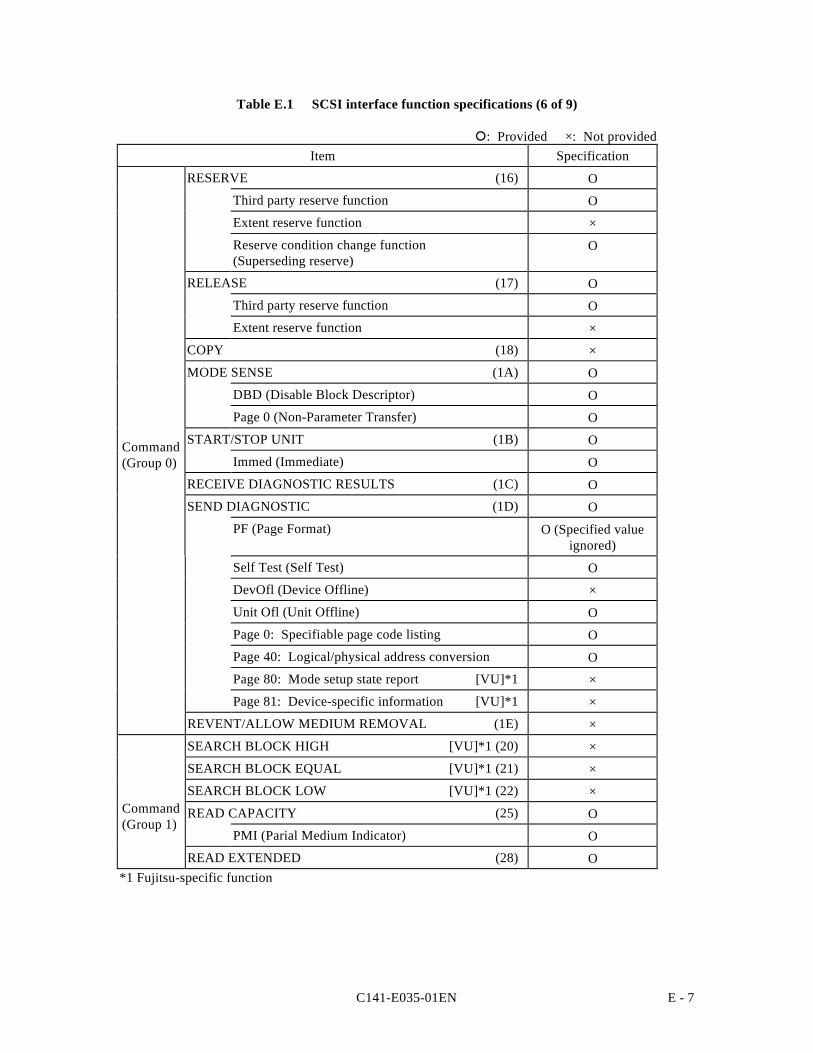
C141-E035-01EN E - 7
Table E.1 SCSI interface function specifications (6 of 9)
: Provided ×: Not providedItem Specification
RESERVE (16) Ο
Third party reserve function Ο
Extent reserve function ×
Reserve condition change function(Superseding reserve)
Ο
RELEASE (17) Ο
Third party reserve function Ο
Extent reserve function ×
COPY (18) ×
MODE SENSE (1A) Ο
DBD (Disable Block Descriptor) Ο
Page 0 (Non-Parameter Transfer) Ο
START/STOP UNIT (1B) Ο
Immed (Immediate) Ο
RECEIVE DIAGNOSTIC RESULTS (1C) Ο
SEND DIAGNOSTIC (1D) Ο
PF (Page Format) Ο (Specified valueignored)
Self Test (Self Test) Ο
DevOfl (Device Offline) ×
Unit Ofl (Unit Offline) Ο
Page 0: Specifiable page code listing Ο
Page 40: Logical/physical address conversion Ο
Page 80: Mode setup state report [VU]*1 ×
Page 81: Device-specific information [VU]*1 ×
REVENT/ALLOW MEDIUM REMOVAL (1E) ×
SEARCH BLOCK HIGH [VU]*1 (20) ×
SEARCH BLOCK EQUAL [VU]*1 (21) ×
SEARCH BLOCK LOW [VU]*1 (22) ×
READ CAPACITY (25) Ο
PMI (Parial Medium Indicator) Ο
READ EXTENDED (28) Ο*1 Fujitsu-specific function
Command(Group 1)
Command(Group 0)
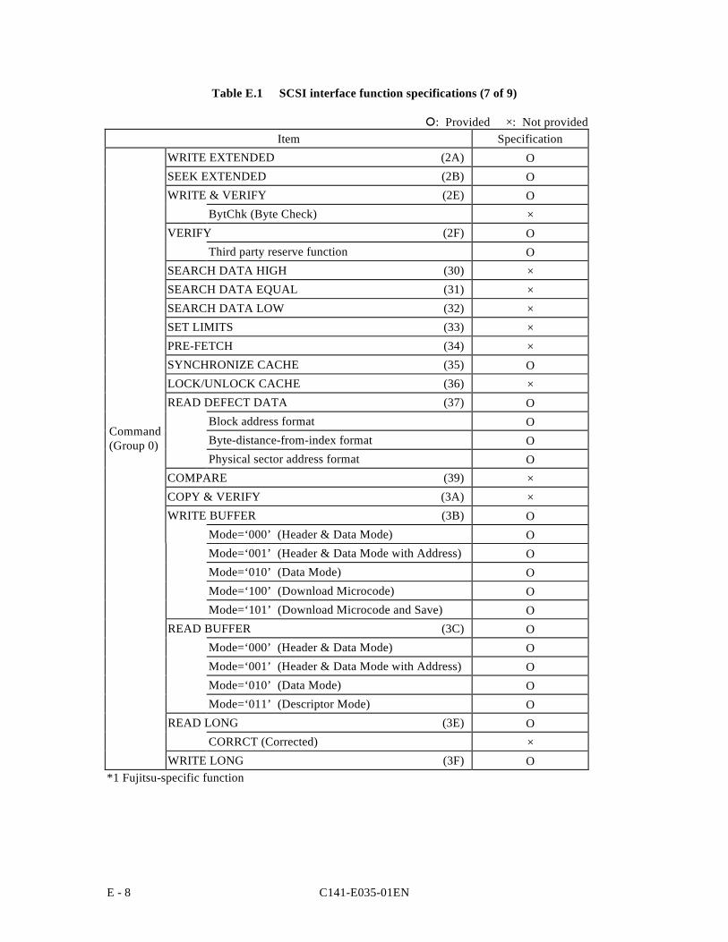
C141-E035-01ENE - 8
Table E.1 SCSI interface function specifications (7 of 9)
: Provided ×: Not providedItem Specification
WRITE EXTENDED (2A) ΟSEEK EXTENDED (2B) ΟWRITE & VERIFY (2E) Ο
BytChk (Byte Check) ×VERIFY (2F) Ο
Third party reserve function ΟSEARCH DATA HIGH (30) ×SEARCH DATA EQUAL (31) ×SEARCH DATA LOW (32) ×SET LIMITS (33) ×PRE-FETCH (34) ×SYNCHRONIZE CACHE (35) ΟLOCK/UNLOCK CACHE (36) ×READ DEFECT DATA (37) Ο
Block address format ΟByte-distance-from-index format ΟPhysical sector address format Ο
COMPARE (39) ×COPY & VERIFY (3A) ×WRITE BUFFER (3B) Ο
Mode=‘000’ (Header & Data Mode) ΟMode=‘001’ (Header & Data Mode with Address) ΟMode=‘010’ (Data Mode) ΟMode=‘100’ (Download Microcode) ΟMode=‘101’ (Download Microcode and Save) Ο
READ BUFFER (3C) ΟMode=‘000’ (Header & Data Mode) ΟMode=‘001’ (Header & Data Mode with Address) ΟMode=‘010’ (Data Mode) ΟMode=‘011’ (Descriptor Mode) Ο
READ LONG (3E) ΟCORRCT (Corrected) ×
WRITE LONG (3F) Ο*1 Fujitsu-specific function
Command(Group 0)
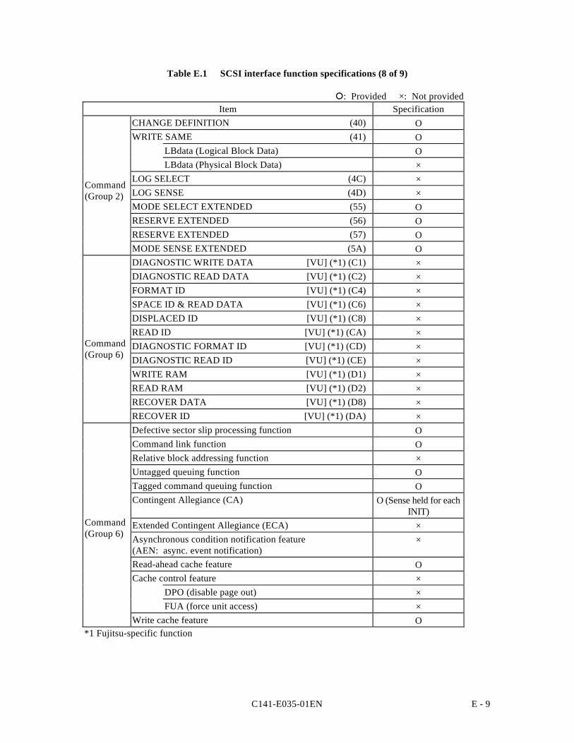
C141-E035-01EN E - 9
Table E.1 SCSI interface function specifications (8 of 9)
: Provided ×: Not providedItem Specification
CHANGE DEFINITION (40) ΟWRITE SAME (41) Ο
LBdata (Logical Block Data) ΟLBdata (Physical Block Data) ×
LOG SELECT (4C) ×LOG SENSE (4D) ×MODE SELECT EXTENDED (55) ΟRESERVE EXTENDED (56) ΟRESERVE EXTENDED (57) ΟMODE SENSE EXTENDED (5A) ΟDIAGNOSTIC WRITE DATA [VU] (*1) (C1) ×DIAGNOSTIC READ DATA [VU] (*1) (C2) ×FORMAT ID [VU] (*1) (C4) ×SPACE ID & READ DATA [VU] (*1) (C6) ×DISPLACED ID [VU] (*1) (C8) ×READ ID [VU] (*1) (CA) ×DIAGNOSTIC FORMAT ID [VU] (*1) (CD) ×DIAGNOSTIC READ ID [VU] (*1) (CE) ×WRITE RAM [VU] (*1) (D1) ×READ RAM [VU] (*1) (D2) ×RECOVER DATA [VU] (*1) (D8) ×RECOVER ID [VU] (*1) (DA) ×Defective sector slip processing function ΟCommand link function ΟRelative block addressing function ×Untagged queuing function ΟTagged command queuing function ΟContingent Allegiance (CA) Ο (Sense held for each
INIT)Extended Contingent Allegiance (ECA) ×Asynchronous condition notification feature(AEN: async. event notification)
×
Read-ahead cache feature ΟCache control feature ×
DPO (disable page out) ×FUA (force unit access) ×
Write cache feature Ο*1 Fujitsu-specific function
Command(Group 6)
Command(Group 6)
Command(Group 2)
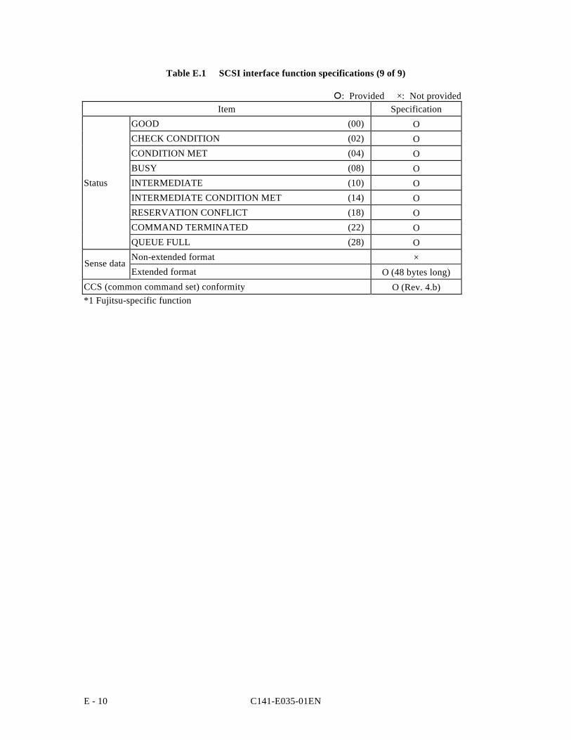
C141-E035-01ENE - 10
Table E.1 SCSI interface function specifications (9 of 9)
: Provided ×: Not providedItem Specification
GOOD (00) ΟCHECK CONDITION (02) ΟCONDITION MET (04) ΟBUSY (08) Ο
Status INTERMEDIATE (10) ΟINTERMEDIATE CONDITION MET (14) ΟRESERVATION CONFLICT (18) ΟCOMMAND TERMINATED (22) ΟQUEUE FULL (28) ΟNon-extended format ×Extended format Ο (48 bytes long)
CCS (common command set) conformity Ο (Rev. 4.b)*1 Fujitsu-specific function
Sense data


FUJITSU LIMITEDOEM Marketing4-1-1, Kamikodanaka, Nakahara-Ku, Kawasaki,211-88, JapanTEL: 044-754-8632FAX: 044-754-8634
FUJITSU COMPUTER PRODUCTS OF AMERICA, INC.2904 Orchard Parkway, San Jose,California 95134-2009, U.S.A.TEL: 1-408-432-6333FAX: 1-408-432-3908
FUJITSU CANADA INC.2800 Matheson Blvd. East, Mississauga, Toronto,Ontario L4W 4X5, CANADATEL: 1-905-602-5454FAX: 1-905-602-5457
FUJITSU EUROPE LIMITED2, Longwalk Road, Stockley Park, Uxbridge,Middlesex UB11 1AB, ENGLANDTEL: 44-81-573-4444FAX: 44-81-573-2643
FUJITSU DEUTSCHLAND GmbHFrankfurter Ring 211, 80807 München, GERMANYTEL: 49-89-323780FAX: 49-89-32378100
FUJITSU NORDIC ABKung Hans Väg, S-191 76 Sollentura, SWEDENTEL: 46-(0)8-6266000FAX: 46-8-626-6010
FUJITSU ITALIA S.p.A.Via Meichiorre Gioia, 8, 20124 Milano, ITALYTEL: 39-2-63651FAX: 39-2-6572257
FUJITSU FRANCE S.A.Batiment Aristote, rue Olof Palme-94006,Créteil cedex, FRANCETEL: 33-1-45-13-16-16FAX: 33-1-43-99-07-00FUJITSU ESPAÑA S.A.
C/ Almagro 40, 28010 Madrid, SPAINTEL: 34-1-581-8100FAX: 34-1-581-8125
FUJITSU AUSTRALIA LIMITED475 Victoria Avenue, Chatswood, 2067 N.S.W, AUSTRALIATEL: 61-2-410-4555FAX: 61-2-411-8603, 8362
FUJITSU HONG KONG LIMITEDRoom 2521, Sun Hung Kai Centre, Harbour Road 30, HONGHONGTEL: 852-827-5780FAX: 852-827-4724
FUJITSU KOREA LIMITED6th Floor, Duk-Heung Bldg., 1328-10, Seocho-Dong, Seocho-Ku,Seoul, KOREATEL: 82-2-739-3281FAX: 82-2-739-3294
FUJITSU (SINGAPORE) PTE. LTD75 Science Park Drive, #02-06 CINTECH II,Singapore 0511, REPUBLIC OF SINGAPORETEL: 65-777-6577FAX: 65-777-8794
FUJITSU TAIWAN LTD.8F, Hun Tai Center Bldg., 170 Tun Hwa N. Rd.,1st Sec., Taipei, TAIWAN R.O.CTEL: 886-2-545-7700FAX: 886-2-717-4644
10
Comments concerning this manual can be directed to one of the following addresses:

Reader Comment FormWe would appreciate your comments and suggestions for improving this publication.
Publication No. Rev. Letter Title Current Date
How did you use this publication? Is the material presented effectively?
What is your overall rating of this publication? What is your occupation?
Your other comments may be entered here. Please be specific and give page,paragraph and line number references where applicable.
Your Name & Return Address
Sales
OperatingInstalling
Maintaining
Learning
Reference
Fair
Poor
Very Good
GoodVery Poor
Fullycovered
WellIllustrated
Thank you for your interest. Please send this sheet to one of the addresses in the left page.
WellOrganized
Clean
FUJITSU LIMITED