Embed Size (px)
Citation preview
C141-E057-02EN
MHE2064AT, MHE2043ATMHF2043AT, MHF2021AT
DISK DRIVE
PRODUCT MANUAL
C141-E057-01EN
FOR SAFE OPERATIONHandling of This Manual
This manual contains important information for using this product. Read thoroughly before usingthe product. Use this product only after thoroughly reading and understanding especially thesection “Important Alert Items” in this manual. Keep this manual handy, and keep it carefully.
FUJITSU makes every effort to prevent users and bystanders from being injured or from sufferingdamage to their property. Use the product according to this manual.
IMPORTANT NOTE TO USERS
READ THE ENTIRE MANUAL CAREFULLY BEFORE USING THIS PRODUCT.INCORRECT USE OF THE PRODUCT MAY RESULT IN INJURY OR DAMAGE TOUSERS, BYSTANDERS OR PROPERTY.
While FUJITSU has sought to ensure the accuracy of all information in this manual, FUJITSUassumes no liability to any party for any damage caused by any error or omission contained in thismanual, its updates or supplements, whether such errors or omissions result from negligence,accident, or any other cause. In addition, FUJITSU assumes no liability with respect to theapplication or use of any product or system in accordance with the descriptions or instructionscontained herein; including any liability for incidental or consequential damages arising therefrom.FUJITSU DISCLAIMS ALL WARRANTIES REGARDING THE INFORMATIONCONTAINED HEREIN, WHETHER EXPRESSED, IMPLIED, OR STATUTORY.
FUJITSU reserves the right to make changes to any products described herein without furthernotice and without obligation.
The contents of this manual may be revised without prior notice.
The contents of this manual shall not be disclosed in any way or reproduced in any media withoutthe express written permission of Fujitsu Limited.
All Rights Reserved, Copyright FUJITSU LIMITED 1998

This page is intentionally left blank.
C141-E057-02EN
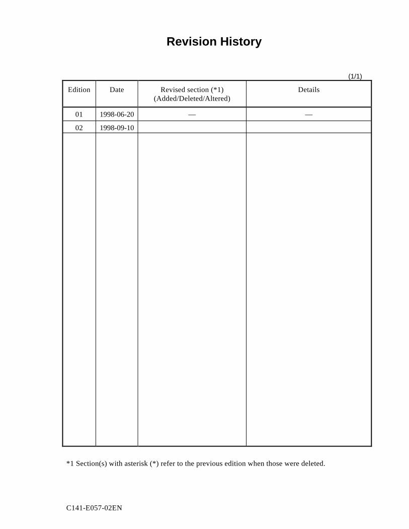
Revision History
(1/1)
Edition Date Revised section (*1)(Added/Deleted/Altered)
Details
01 1998-06-20 — —
02 1998-09-10
*1 Section(s) with asterisk (*) refer to the previous edition when those were deleted.

This page is intentionally left blank.
C141-E057-01EN i
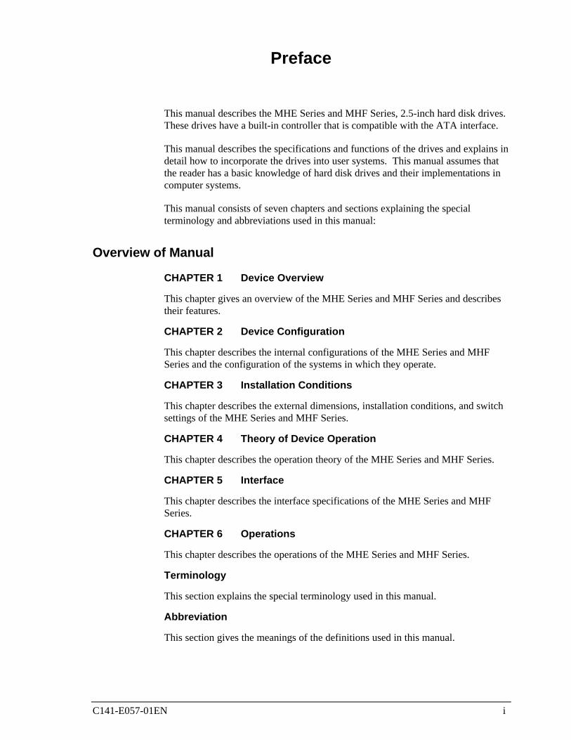
Preface
This manual describes the MHE Series and MHF Series, 2.5-inch hard disk drives.These drives have a built-in controller that is compatible with the ATA interface.
This manual describes the specifications and functions of the drives and explains indetail how to incorporate the drives into user systems. This manual assumes thatthe reader has a basic knowledge of hard disk drives and their implementations incomputer systems.
This manual consists of seven chapters and sections explaining the specialterminology and abbreviations used in this manual:
Overview of Manual
CHAPTER 1 Device Overview
This chapter gives an overview of the MHE Series and MHF Series and describestheir features.
CHAPTER 2 Device Configuration
This chapter describes the internal configurations of the MHE Series and MHFSeries and the configuration of the systems in which they operate.
CHAPTER 3 Installation Conditions
This chapter describes the external dimensions, installation conditions, and switchsettings of the MHE Series and MHF Series.
CHAPTER 4 Theory of Device Operation
This chapter describes the operation theory of the MHE Series and MHF Series.
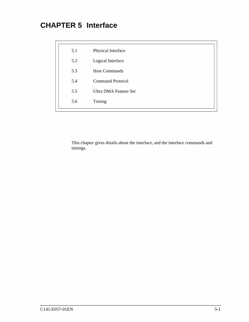
CHAPTER 5 Interface
This chapter describes the interface specifications of the MHE Series and MHFSeries.
CHAPTER 6 Operations
This chapter describes the operations of the MHE Series and MHF Series.
Terminology
This section explains the special terminology used in this manual.
Abbreviation
This section gives the meanings of the definitions used in this manual.
Preface
ii C141-E057-01EN
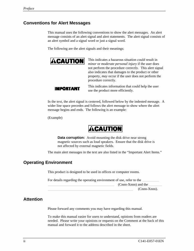
Conventions for Alert Messages
This manual uses the following conventions to show the alert messages. An alertmessage consists of an alert signal and alert statements. The alert signal consists ofan alert symbol and a signal word or just a signal word.
The following are the alert signals and their meanings:
This indicates a hazarous situation could result inminor or moderate personal injury if the user doesnot perform the procedure correctly. This alert signalalso indicates that damages to the product or otherproperty, may occur if the user does not perform theprocedure correctly.
This indicates information that could help the useruse the product more efficiently.
In the text, the alert signal is centered, followed below by the indented message. Awider line space precedes and follows the alert message to show where the alertmessage begins and ends. The following is an example:
(Example)
Data corruption: Avoid mounting the disk drive near strongmagnetic sources such as loud speakers. Ensure that the disk drive isnot affected by external magnetic fields.
The main alert messages in the text are also listed in the “Important Alert Items.”
Operating Environment
This product is designed to be used in offices or computer rooms.
For details regarding the operating environment of use, refer to the (Cnnn-Xnnn) and the (Cnnn-Xnnn).
Attention
Please forward any comments you may have regarding this manual.
To make this manual easier for users to understand, opinions from readers areneeded. Please write your opinions or requests on the Comment at the back of thismanual and forward it to the address described in the sheet.
Preface
C141-E057-01EN iii
Liability Exception
“Disk drive defects” refers to defects that involve adjustment, repair, orreplacement.
Fujitsu is not liable for any other disk drive defects, such as those caused by usermisoperation or mishandling, inappropriate operating environments, defects in thepower supply or cable, problems of the host system, or other causes outside thedisk drive.

This page is intentionally left blank.
C141-E057-02EN v
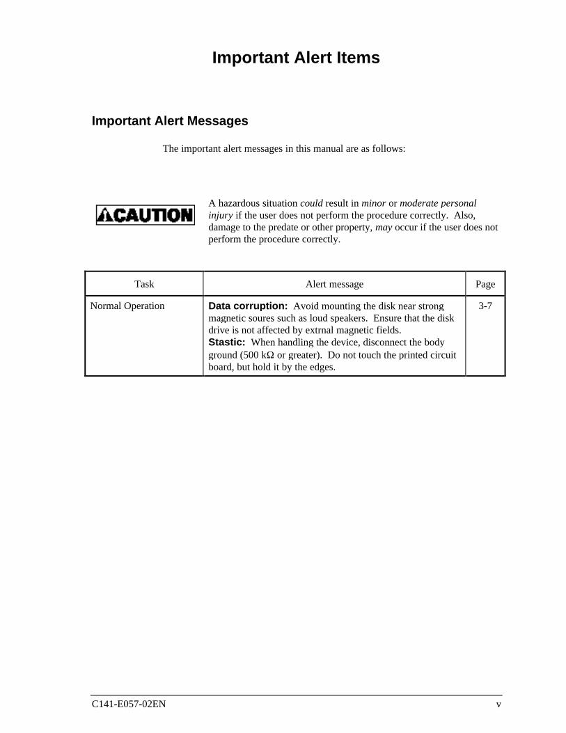
Important Alert Items
Important Alert Messages
The important alert messages in this manual are as follows:
A hazardous situation could result in minor or moderate personalinjury if the user does not perform the procedure correctly. Also,damage to the predate or other property, may occur if the user does notperform the procedure correctly.
Task Alert message Page
Normal Operation Data corruption: Avoid mounting the disk near strongmagnetic soures such as loud speakers. Ensure that the diskdrive is not affected by extrnal magnetic fields.Stastic: When handling the device, disconnect the bodyground (500 kΩ or greater). Do not touch the printed circuitboard, but hold it by the edges.
3-7

This page is intentionally left blank.
C141-E057-02EN vii
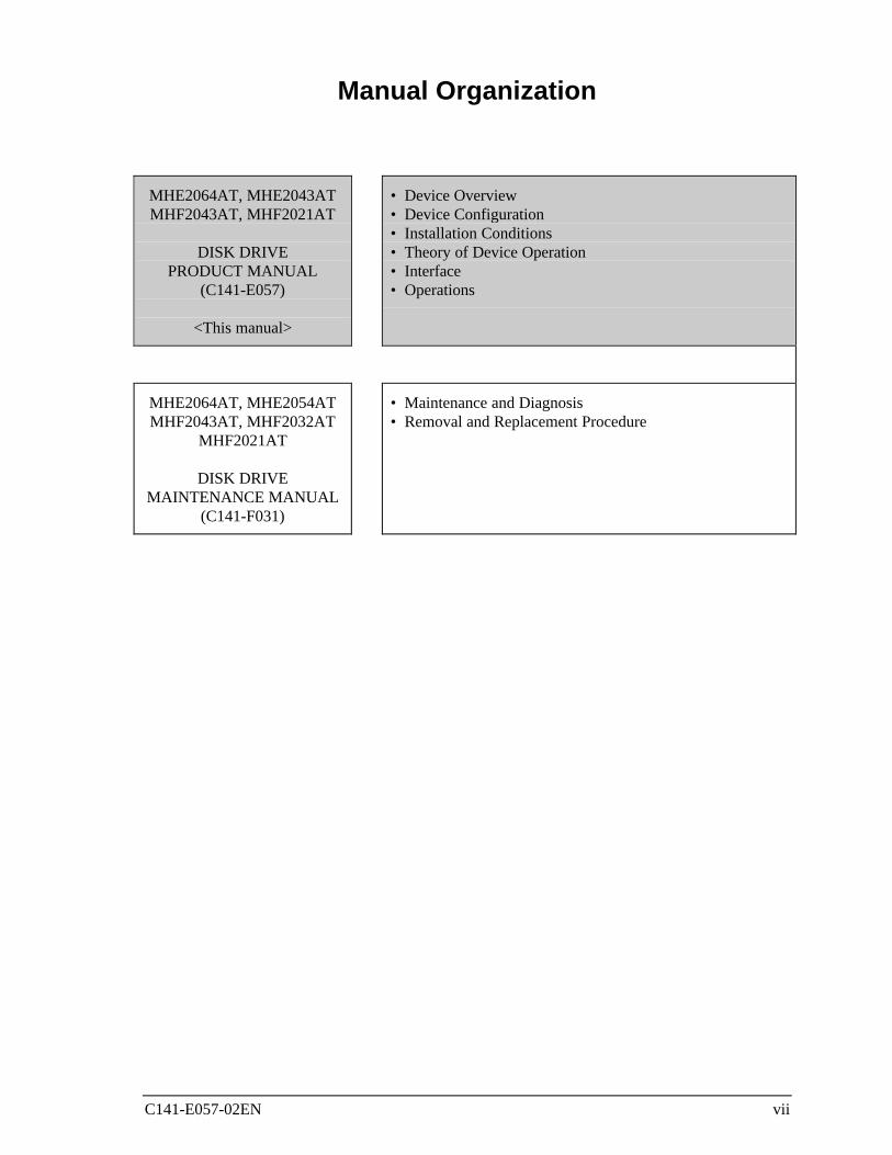
Manual Organization
MHE2064AT, MHE2043ATMHF2043AT, MHF2021AT
DISK DRIVEPRODUCT MANUAL
(C141-E057)
<This manual>
• Device Overview• Device Configuration• Installation Conditions• Theory of Device Operation• Interface• Operations
MHE2064AT, MHE2054ATMHF2043AT, MHF2032AT
MHF2021AT
DISK DRIVEMAINTENANCE MANUAL
(C141-F031)
• Maintenance and Diagnosis• Removal and Replacement Procedure

This page is intentionally left blank.
C141-E057-01EN ix
Contents
CHAPTER 1 Device Overview........................................................................ 1-1
1.1 Features 1-2
1.1.1 Functions and performance 1-2
1.1.2 Adaptability 1-2
1.1.3 Interface 1-3
1.2 Device Specifications 1-4
1.2.1 Specifications summary 1-4
1.2.2 Model and product number 1-6
1.3 Power Requirements 1-6
1.4 Environmental Specifications 1-8
1.5 Acoustic Noise 1-9
1.6 Shock and Vibration 1-9
1.7 Reliability 1-10
1.8 Error Rate 1-11
1.9 Media Defects 1-11
CHAPTER 2 Device Configuration................................................................ 2-1
2.1 Device Configuration 2-2
2.2 System Configuration 2-4
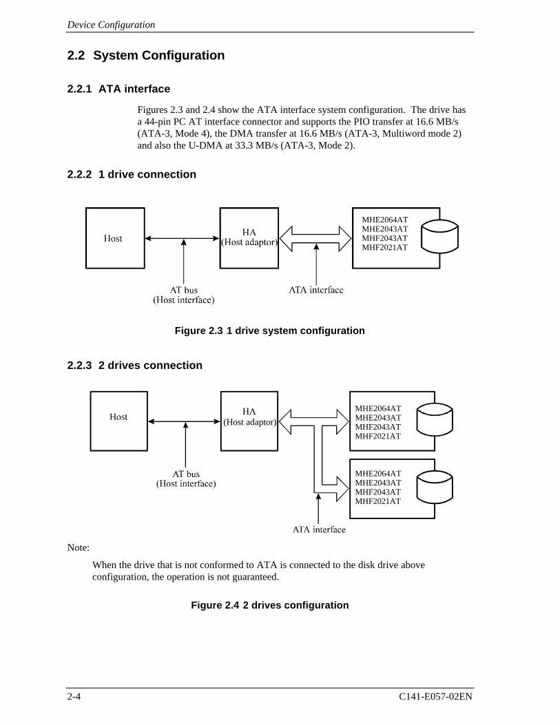
2.2.1 ATA interface 2-4
2.2.2 1 drive connection 2-4
2.2.3 2 drives connection 2-4
Contents
x C141-E057-01EN
CHAPTER 3 Installation Conditions..............................................................3-1
3.1 Dimensions 3-2
3.2 Mounting 3-4
3.3 Cable Connections 3-8
3.3.1 Device connector 3-8
3.3.2 Cable connector specifications 3-9
3.3.3 Device connection 3-9
3.3.4 Power supply connector (CN1) 3-10
3.4 Jumper Settings 3-10
3.4.1 Location of setting jumpers 3-10
3.4.2 Factory default setting 3-11
3.4.3 Master drive-slave drive setting 3-11
3.4.4 CSEL setting 3-12
CHAPTER 4 Theory of Device Operation......................................................4-1
4.1 Outline 4-2
4.2 Subassemblies 4-2
4.2.1 Disk 4-2
4.2.2 Head 4-2
4.2.3 Spindle 4-3
4.2.4 Actuator 4-3
4.2.5 Air filter 4-3
4.3 Circuit Configuration 4-4
4.4 Power-on Sequence 4-6
4.5 Self-calibration 4-7
4.5.1 Self-calibration contents 4-7
4.5.2 Execution timing of self-calibration 4-8
4.5.3 Command processing during self-calibration 4-9
4.6 Read/write Circuit 4-9
Contents
C141-E057-01EN xi
4.6.1 Read/write preamplifier (PreAMP) 4-9
4.6.2 Write circuit 4-10
4.6.3 Read circuit 4-12
4.6.4 Digital PLL circuit 4-13
4.7 Servo Control 4-14
4.7.1 Servo control circuit 4-14
4.7.2 Data-surface servo format 4-18
4.7.3 Servo frame format 4-18
4.7.4 Actuator motor control 4-19
4.7.5 Spindle motor control 4-20
CHAPTER 5 Interface ..................................................................................... 5-1
5.1 Physical Interface 5-2
5.1.1 Interface signals 5-2
5.1.2 Signal assignment on the connector 5-3
5.2 Logical Interface 5-6
5.2.1 I/O registers 5-7
5.2.2 Command block registers 5-8
5.2.3 Control block registers 5-13
5.3 Host Commands 5-13
5.3.1 Command code and parameters 5-14
5.3.2 Command descriptions 5-16
5.3.3 Error posting 5-71
5.4 Command Protocol 5-73
5.4.1 Data transferring commands from device to host 5-73
5.4.2 Data transferring commands from host to device 5-75
5.4.3 Commands without data transfer 5-77
5.4.4 Other commands 5-78
5.4.5 DMA data transfer commands 5-78
5.5 Ultra DMA Feature Set 5-80
5.5.1 Overview 5-80
Contents
xii C141-E057-01EN
5.5.2 Phases of operation 5-81
5.5.2.1 Ultra DMA burst initiation phase 5-81
5.5.2.2 Data transfer phase 5-82
5.5.2.3 Ultra DMA burst termination phase 5-82
5.5.3 Ultra DMA data in commands 5-83
5.5.3.1 Initiating an Ultra DMA data in burst 5-83
5.5.3.2 The data in transfer 5-84
5.5.3.3 Pausing an Ultra DMA data in burst 5-84
5.5.3.4 Terminating an Ultra DMA data in burst 5-85
5.5.4 Ultra DMA data out commands 5-88
5.5.4.1 Initiating an Ultra DMA data out burst 5-88
5.5.4.2 The data out transfer 5-88
5.5.4.3 Pausing an Ultra DMA data out burst 5-89
5.5.4.4 Terminating an Ultra DMA data out burst 5-90
5.5.5 Ultra DMA CRC rules 5-92
5.5.6 Series termination required for Ultra DMA 5-94
5.6 Timing 5-95
5.6.1 PIO data transfer 5-95
5.6.2 Single word DMA data transfer 5-97
5.6.3 Multiword DMA data transfer 5-98
5.6.4 Transfer of Ultra DMA data 5-99
5.6.4.1 Starting of Ultra DMA data In Burst 5-99
5.6.4.2 Ultra DMA data burst timing requirements 5-100
5.6.4.3 Sustained Ultra DMA data in burst 5-102
5.6.4.4 Host pausing an Ultra DMA data in burst 5-103
5.6.4.5 Device terminating an Ultra DMA data in burst 5-104
5.6.4.6 Host terminating an Ultra DMA data in burst 5-105
5.6.4.7 Initiating an Ultra DMA data out burst 5-106
5.6.4.8 Sustained Ultra DMA data out burst 5-107
5.6.4.9 Device pausing an Ultra DMA data out burst 5-108
5.6.4.10 Host terminating an Ultra DMA data out burst 5-109
5.6.4.11 Device terminating an Ultra DMA data in burst 5-110
5.6.5 Power-on and reset 5-111
Contents
C141-E057-01EN xiii
CHAPTER 6 Operations ................................................................................. 6-1
6.1 Device Response to the Reset 6-2
6.1.1 Response to power-on 6-2
6.1.2 Response to hardware reset 6-4
6.1.3 Response to software reset 6-5
6.1.4 Response to diagnostic command 6-6
6.2 Address Translation 6-7
6.2.1 Default parameters 6-7
6.2.2 Logical address 6-8
6.3 Power Save 6-9
6.3.1 Power save mode 6-9
6.3.2 Power commands 6-11
6.4 Defect Management 6-11
6.4.1 Spare area 6-12
6.4.2 Alternating defective sectors 6-12
6.5 Read-Ahead Cache 6-14
6.5.1 Data buffer configuration 6-14
6.5.2 Caching operation 6-14
6.5.3 Usage of read segment 6-16
6.5.3.1 Mis-hit (no hit) 6-16
6.5.3.2 Sequential read 6-17
6.5.3.3 Full hit (hit all) 6-20
6.5.3.4 Partially hit 6-21
6.6 Write Cache 6-22
Glossary ................................................................................................. GL-1
Acronyms and Abbreviations ........................................................................ AB-1
Index ...................................................................................................IN-1
Contents
xiv C141-E057-01EN
Illustrations
Figures
Figure 1.1 Current fluctuation (Typ.) at +5V when power is turned on 1-7
Figure 2.1 Disk drive outerview (the MHE Series and MHF Series) 2-2Figure 2.2 Configuration of disk media heads 2-3Figure 2.3 1 drive system configuration 2-4Figure 2.4 2 drives configuration 2-4
Figure 3.1 Dimensions (MHE/MHF series) 3-2Figure 3.2 Orientation (Sample: MHE2064AT) 3-4Figure 3.3 Mounting frame structure 3-5Figure 3.4 Surface temperature measurement points (Sample: MHE2064AT)
3-6Figure 3.5 Service area (Sample: MHE2064AT) 3-7Figure 3.6 Connector locations (Sample: MHE2064AT) 3-8Figure 3.7 Cable connections 3-9Figure 3.8 Power supply connector pins (CN1) 3-10Figure 3.9 Jumper location 3-10Figure 3.10 Factory default setting 3-11Figure 3.11 Jumper setting of master or slave device 3-11Figure 3.12 CSEL setting 3-12Figure 3.13 Example (1) of Cable Select 3-12Figure 3.14 Example (2) of Cable Select 3-13
Figure 4.1 Head structure 4-3Figure 4.2 Circuit Configuration 4-5Figure 4.3 Power-on operation sequence 4-7Figure 4.4 Read/write circuit block diagram 4-11Figure 4.5 Frequency characteristic of programmable filter 4-12Figure 4.6 Block diagram of servo control circuit 4-14Figure 4.7 Physical sector servo configuration on disk surface 4-16Figure 4.8 Servo frame format 4-18
Figure 5.1 Interface signals 5-2Figure 5.2 Execution example of READ MULTIPLE command 5-20Figure 5.3 Read Sector(s) command protocol 5-74Figure 5.4 Protocol for command abort 5-75
Contents
C141-E057-02EN xv
Figure 5.5 WRITE SECTOR(S) command protocol 5-76Figure 5.6 Protocol for the command execution without data transfer 5-
78Figure 5.7 Normal DMA data transfer 5-79Figure 5.8 An example of generation of parallel CRC 5-93Figure 5.9 Ultra DMA termination with pull-up or pull-down 5-94Figure 5.10 Data transfer timing 5-96Figure 5.11 Single word DMA data transfer timing (mode 2) 5-97Figure 5.12 Multiword DMA data transfer timing (mode 2) 5-98Figure 5.13 Starting of Ultra DMA data In Burst transfer 5-99Figure 5.14 Sustained Ultra DMA data in burst 5-102Figure 5.15 Host pausing an Ultra DMA data in burst 5-103Figure 5.16 Device terminating an Ultra DMA data in burst 5-104Figure 5.17 Host terminating an Ultra DMA data in burst 5-105Figure 5.18 Initiating an Ultra DMA data out burst 5-106Figure 5.19 Sustained Ultra DMA data out burst 5-107Figure 5.20 Device pausing an Ultra DMA data out burst 5-108Figure 5.21 Host terminating an Ultra DMA data out burst 5-109Figure 5.22 Device terminating an Ultra DMA data out burst 5-110Figure 5.23 Power on Reset Timing 5-111
Figure 6.1 Response to power-on 6-3Figure 6.2 Response to hardware reset 6-4Figure 6.3 Response to software reset 6-5Figure 6.4 Response to diagnostic command 6-6Figure 6.5 Address translation (example in CHS mode) 6-8Figure 6.6 Address translation (example in LBA mode) 6-9Figure 6.7 Sector slip processing 6-12Figure 6.8 Alternate cylinder assignment 6-13Figure 6.9 Data buffer configuration 6-14
Tables
Table 1.1 Specifications (MHE2064AT/MHE2043AT) 1-4Table 1.2 Specifications (MHF2043AT/MHF2021AT) 1-5Table 1.3 Specifications (MHE2064AT/2043AT/MHF2043AT/2021AT)
1-6Table 1.4 Model names and product numbers 1-6Table 1.5 Current and power dissipation 1-7Table 1.6 Environmental specifications 1-8Table 1.7 Acoustic noise specification 1-9Table 1.8 Shock and vibration specification 1-9
Contents
xvi C141-E057-01EN
Table 3.1 Surface temperature measurement points and standard values3-6
Table 3.2 Cable connector specifications 3-9
Table 4.1 Self-calibration execution timechart 4-9Table 4.2 Write precompensation algorithm 4-10
Table 5.1 Signal assignment on the interface connector 5-3Table 5.2 I/O registers 5-7Table 5.3 Command code and parameters 5-14Table 5.4 Information to be read by IDENTIFY DEVICE command 5-
32Table 5.5 Features register values and settable modes 5-39Table 5.6 Diagnostic code 5-46Table 5.7 Features Register values (subcommands) and functions 5-57Table 5.8 Format of device attribute value data 5-59Table 5.9 Format of insurance failure threshold value data 5-60Table 5.10 Contents of security password 5-64Table 5.11 Contents of SECURITY SET PASSWORD data 5-68Table 5.12 Relationship between combination of Identifier and Security
level, and operation of the lock function 5-69Table 5.13 Command code and parameters 5-71Table 5.14 Parallel generation equation of CRC polynomial 5-93Table 5.15 Recommended series termination for Ultra DMA 5-94Table 5.16 Ultra DMA data burst timing requirements 5-100
Table 6.1 Default parameters 6-7
C141-E057-01EN 1-1
CHAPTER 1 Device Overview
1.1 Features
1.2 Device Specifications
1.3 Power Requirements
1.4 Environmental Specifications
1.5 Acoustic Noise
1.6 Shock and Vibration
1.7 Reliability
1.8 Error Rate
1.9 Media Defects
Overview and features are described in this chapter, and specifications and powerrequirement are described.
The MHE Series and MHF Series are 2.5-inch hard disk drives with built-in diskcontrollers. These disk drives use the AT-bus hard disk interface protocol and arecompact and reliable.
Device Overview
1-2 C141-E057-02EN
1.1 Features
1.1.1 Functions and performance
The fillowing features of the MHE Series and MHF Series are described.
(1) Compact
The MHE2064AT and MHE2043AT have 3 disks, and its height is 12.5 mm(0.492 inch). The MHF2043AT and MHF2021AT have 1 disk or 2 disks of 65mm (2.5 inches) diameter, and its height is 9.5 mm (0.374 inch).
(2) Large capacity
The disk drive can record up to 2.16 GB (formatted) on one disk using the (16/17)EPR4ML recording method and 14 recording zone technology. The MHE Seriesand MHF Series have a formatted capacity of 6.49 GB (MHE2064AT), 4.32 GB(MHE2043AT), 4.32 GB (MHF2043AT), 2.16 GB (MHF2021AT) respectively.
(3) High-speed Transfer rate
The disk drives (the MHE Series and MHF Series) have an internal data rate up to13.6 MB/s. The disk drive supports an external data rate up to 33.3 MB/s (U-DMA mode 2).
(4) Average positioning time
Use of a rotary voice coil motor in the head positioning mechanism greatlyincreases the positioning speed. The average positioning time is 13 ms (at read).
1.1.2 Adaptability
(1) Power save mode
The power save mode feature for idle operation, stand by and sleep modes makesThe disk drives (the MHE Series and MHF Series) ideal for applications wherepower consumption is a factor.
(2) Wide temperature range
The disk drives (the MHE Series and MHF Series) can be used over a widetemperature range (5°C to 55°C).
(3) Low noise and vibration
In Ready status, the noise of the disk drives (the MHE Series and MHF Series) isonly about 30 dBA (measured at 1 m apart from the drive under the idle mode).
1.1 Features
C141-E057-01EN 1-3
1.1.3 Interface
(1) Connection to interface
With the built-in ATA interface controller, the disk drives (the MHE Series andMHF Series) can be connected to an ATA interface of a personal computer.
(2) 512-KB data buffer
The disk drives (the MHE Series and MHF Series) uses a 512-KB data buffer totransfer data between the host and the disk media.
In combination with the read-ahead cache system described in item (3) and thewrite cache described in item (7), the buffer contributes to efficient I/Oprocessing.
(3) Read-ahead cache system
After the execution of a disk read command, the disk drive automatically reads thesubsequent data block and writes it to the data buffer (read ahead operation). Thiscache system enables fast data access. The next disk read command wouldnormally cause another disk access. But, if the read ahead data corresponds to thedata requested by the next read command, the data in the buffer can be transferredinstead.
(4) Master/slave
The disk drives (the MHE Series and MHF Series) can be connected to ATAinterface as daisy chain configuration. Drive 0 is a master device, drive 1 is aslave device.
(5) Error correction and retry by ECC
If a recoverable error occurs, the disk drives (the MHE Series and MHF Series)themselves attempt error recovery. The ECC has improved buffer error correctionfor correctable data errors.
(6) Self-diagnosis
The disk drives (the MHE Series and MHF Series) have a diagnostic function tocheck operation of the controller and disk drives. Executing the diagnosticcommand invokes self-diagnosis.
(7) Write cache
When the disk drives (the MHE Series and MHF Series) receive a writecommand, the disk drives post the command completion at completion oftransferring data to the data buffer completion of writing to the disk media. Thisfeature reduces the access time at writing.
Device Overview
1-4 C141-E057-02EN
1.2 Device Specifications
1.2.1 Specifications summary
Table 1.1 shows the specfications of the disk drives (MHE2064AT/MHE2043AT).
Table 1.1 Specifications (MHE2064AT/MHE2043AT)
MHE2064AT MHE2043AT
Format Capacity (*1) 6.49 GB 4.32 GB
Number of Heads 6 4
Number of Cylinders (User) 8,647
Bytes per Sector 512
Recording Method (16/17) EPR4ML
Track Density 14,200 TPI
Bit Density 237.8 Kbpi
Rotational Speed 4,200 rpm ± 1%
Average Latency 7.14 ms
Positioning time (read and seek)
• Minimum (Track to Track)
• Average
• Maximum (Full)
1.5 ms (typ.)
Read: 13 ms (typ.)
23 ms (typ.)
Start/Stop time
• Start (0 rpm to Drive Read)
• Stop (at Power Down)
Typ.: 5 sec
Typ.: 5 sec
Interface ATA-4 (Max. Cable length: 0.46 m)
Data Transfer Rate
• To/From Media 7.7 to 13.6 MB/s
• To/From Host 33.3 MB/s Max.(U-DMA mode 2)
Data Buffer Size 512 KB
Physical Dimensions(Height × Width × Depth)
12.5 mm × 100.0 mm ×70.0 mm
Weight 145 g
1.2 Device Specifications
C141-E057-02EN 1-5
Table 1.2 shows the specfications of the disk drives (MHF2043AT/MHF2021AT).
Table 1.2 Specifications (MHF2043AT/MHF2021AT)
MHF2043AT MHF2021AT
Format Capacity (*1) 4.32 GB 2.16 GB
Number of Heads 4 2
Number of Cylinders (User) 8,647
Bytes per Sector 512
Recording Method (16/17) EPR4ML
Track Density 14,200 TPI
Bit Density 237.8 Kbpi
Rotational Speed 4,200 rpm ± 1%
Average Latency 7.14 ms
Positioning time (read and seek)
• Minimum (Track to Track)
• Average
• Maximum (Full)
1.5 ms (typ.)
Read: 13 ms (typ.)
23 ms (typ.)
Start/Stop time
• Start (0 rpm to Drive Read)
• Stop (at Power Down)
Typ.: 5 sec
Typ.: 5 sec
Interface ATA-4 (Max. Cable length: 0.46 m)
Data Transfer Rate
• To/From Media 7.7 to 13.6 MB/s
• To/From Host 33.3 MB/s Max.(U-DMA mode 2)
Data Buffer Size 512 KB
Physical Dimensions(Height × Width × Depth)
9.5 mm × 100.0 mm × 70.0 mm
Weight 98 g
*1: Capacity under the LBA mode.
Device Overview
1-6 C141-E057-02EN
Under the CHS mode (normal BIOS specification), formatted capacity,number of cylinders, number of heads, and number of sectors are asfollows.
Table 1.3 Specifications (MHE2064AT/2043AT/MHF2043AT/2021AT)
Model Formatted Capacity No. of Cylinder No. of Heads No. of Sectors
MHE2064AT 6,495.06 MB 13,424 15 63
MHE2043AT 4,327.46 MB 8,944 15 63
MHF2043AT 4,327.46 MB 8,944 15 63
MHF2021AT 2,167.60 MB 4,200 16 63
1.2.2 Model and product number
Table 1.4 lists the model names and product numbers of the MHE Series andMHF Series.
Table 1.4 Model names and product numbers
Model Name Capacity(user area)
Mounting screw Order No.
MHE2064AT 6.49 GB M3, depth 3 CA01757-B060
MHE2043AT 4.32 GB M3, depth 3 CA01757-B040
MHF2043AT 4.32 GB M3, depth 3 CA01758-B040
MHF2021AT 2.16 GB M3, depth 3 CA01758-B020
1.3 Power Requirements
(1) Input Voltage
• + 5 V ± 5 %
(2) Ripple
+5 V
Maximum 100 mV (peak to peak)
Frequency DC to 1 MHz
1.3 Power Requirements
C141-E057-01EN 1-7
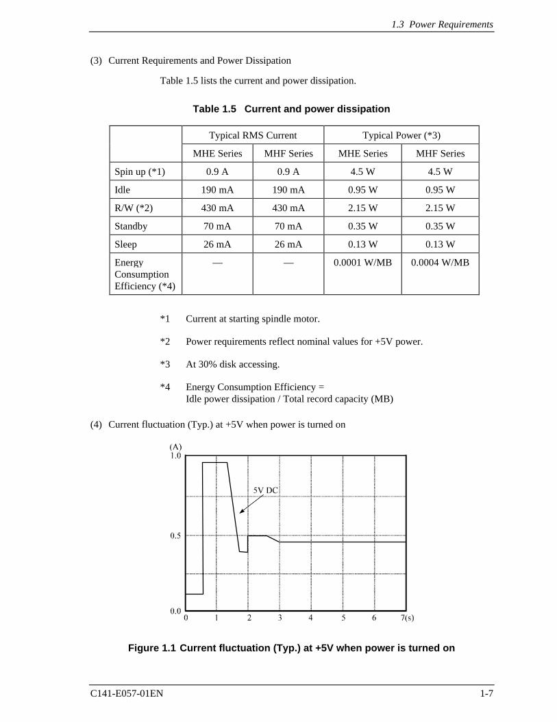
(3) Current Requirements and Power Dissipation
Table 1.5 lists the current and power dissipation.
Table 1.5 Current and power dissipation
Typical RMS Current Typical Power (*3)
MHE Series MHF Series MHE Series MHF Series
Spin up (*1) 0.9 A 0.9 A 4.5 W 4.5 W
Idle 190 mA 190 mA 0.95 W 0.95 W
R/W (*2) 430 mA 430 mA 2.15 W 2.15 W
Standby 70 mA 70 mA 0.35 W 0.35 W
Sleep 26 mA 26 mA 0.13 W 0.13 W
EnergyConsumptionEfficiency (*4)
— — 0.0001 W/MB 0.0004 W/MB
*1 Current at starting spindle motor.
*2 Power requirements reflect nominal values for +5V power.
*3 At 30% disk accessing.
*4 Energy Consumption Efficiency =Idle power dissipation / Total record capacity (MB)
(4) Current fluctuation (Typ.) at +5V when power is turned on
Figure 1.1 Current fluctuation (Typ.) at +5V when power is turned on
Device Overview
1-8 C141-E057-01EN
(5) Power on/off sequence
The voltage detector circuits (the MHE Series and MHF Series) monitor +5 V.The circuits do not allow a write signal if either voltage is abnormal. Theseprevent data from being destroyed and eliminates the need to be concerned withthe power on/off sequence.
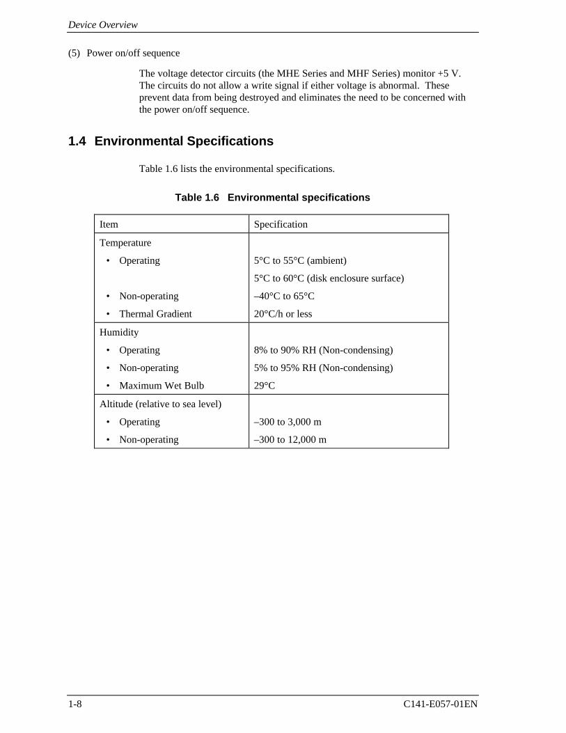
1.4 Environmental Specifications
Table 1.6 lists the environmental specifications.
Table 1.6 Environmental specifications
Item Specification
Temperature
• Operating
• Non-operating
• Thermal Gradient
5°C to 55°C (ambient)
5°C to 60°C (disk enclosure surface)
–40°C to 65°C
20°C/h or less
Humidity
• Operating
• Non-operating
• Maximum Wet Bulb
8% to 90% RH (Non-condensing)
5% to 95% RH (Non-condensing)
29°C
Altitude (relative to sea level)
• Operating
• Non-operating
–300 to 3,000 m
–300 to 12,000 m
1.6 Shock and Vibration
C141-E057-02EN 1-9
1.5 Acoustic Noise
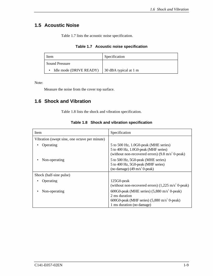
Table 1.7 lists the acoustic noise specification.
Table 1.7 Acoustic noise specification
Item Specification
Sound Pressure
• Idle mode (DRIVE READY) 30 dBA typical at 1 m
Note:
Measure the noise from the cover top surface.
1.6 Shock and Vibration
Table 1.8 lists the shock and vibration specification.
Table 1.8 Shock and vibration specification
Item Specification
Vibration (swept sine, one octave per minute)
• Operating
• Non-operating
5 to 500 Hz, 1.0G0-peak (MHE series)5 to 400 Hz, 1.0G0-peak (MHF series)(without non-recovered errors) (9.8 m/s2 0-peak)
5 to 500 Hz, 5G0-peak (MHE series)5 to 400 Hz, 5G0-peak (MHF series)(no damage) (49 m/s2 0-peak)
Shock (half-sine pulse)
• Operating
• Non-operating
125G0-peak(without non-recovered errors) (1,225 m/s2 0-peak)
600G0-peak (MHE series) (5,880 m/s2 0-peak)2 ms duration600G0-peak (MHF series) (5,880 m/s2 0-peak)1 ms duration (no damage)
Device Overview
1-10 C141-E057-01EN
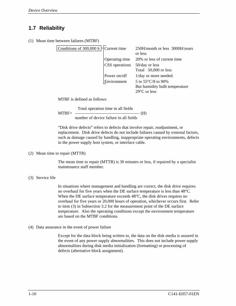
1.7 Reliability
(1) Mean time between failures (MTBF)
Conditions of 300,000 h Current time 250H/month or less 3000H/yearsor less
Operating time 20% or less of current timeCSS operations 50/day or less
Total 50,000 or lessPower on/off 1/day or more needed.Environment 5 to 55°C/8 to 90%
But humidity bulb temperature29°C or less
MTBF is defined as follows:
Total operation time in all fieldsMTBF= (H)
number of device failure in all fields
“Disk drive defects” refers to defects that involve repair, readjustment, orreplacement. Disk drive defects do not include failures caused by external factors,such as damage caused by handling, inappropriate operating environments, defectsin the power supply host system, or interface cable.
(2) Mean time to repair (MTTR)
The mean time to repair (MTTR) is 30 minutes or less, if repaired by a specialistmaintenance staff member.
(3) Service life
In situations where management and handling are correct, the disk drive requiresno overhaul for five years when the DE surface temperature is less than 48°C.When the DE surface temperature exceeds 48°C, the disk drives requires nooverhaul for five years or 20,000 hours of operation, whichever occurs first. Referto item (3) in Subsection 3.2 for the measurement point of the DE surfacetemperature. Also the operating conditions except the environment temperatureare based on the MTBF conditions.
(4) Data assurance in the event of power failure
Except for the data block being written to, the data on the disk media is assured inthe event of any power supply abnormalities. This does not include power supplyabnormalities during disk media initialization (formatting) or processing ofdefects (alternative block assignment).
1.9 Media Defects
C141-E057-02EN 1-11
1.8 Error Rate
Known defects, for which alternative blocks can be assigned, are not included inthe error rate count below. It is assumed that the data blocks to be accessed areevenly distributed on the disk media.
(1) Unrecoverable read error
Read errors that cannot be recovered by maximum read retries of drive withoutuser’s retry and ECC corrections shall occur no more than 10 times when readingdata of 1014 bits. Read retries are executed according to the disk drive’s errorrecovery procedure, and include read retries accompanying head offset operations.
(2) Positioning error
Positioning (seek) errors that can be recovered by one retry shall occur no morethan 10 times in 107 seek operations.
1.9 Media Defects
Defective sectors are replaced with alternates when the disk (the MHE Series andMHF Series) are formatted prior to shipment from the factory (low level format).Thus, the hosts see a defect-free devices.
Alternate sectors are automatically accessed by the disk drive. The user need notbe concerned with access to alternate sectors.

This page is intentionally left blank.
C141-E057-01EN 2-1
CHAPTER 2 Device Configuration
2.1 Device Configuration
2.2 System Configuration
This chapter describes the internal configurations of the hard disk drives and theconfiguration of the systems in which they operate.
Device Configuration
2-2 C141-E057-02EN
2.1 Device Configuration
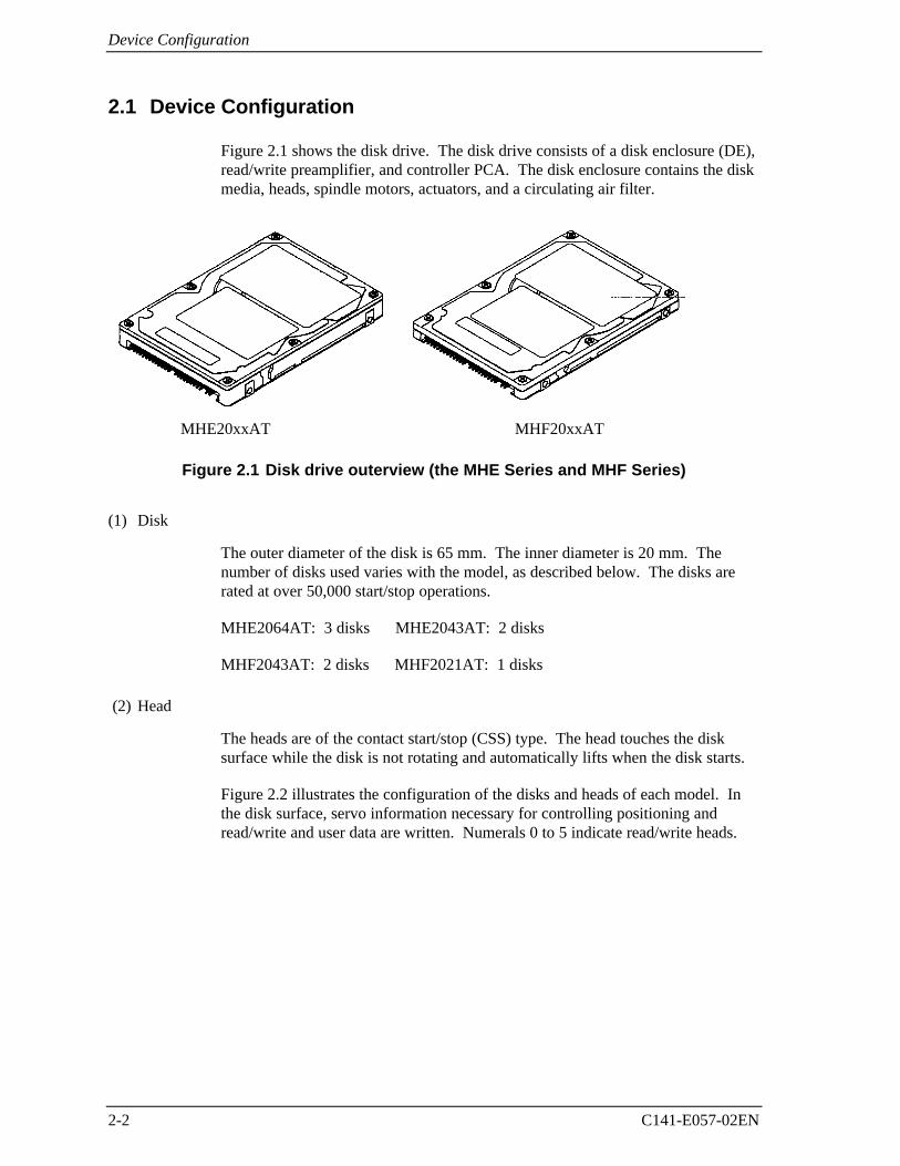
Figure 2.1 shows the disk drive. The disk drive consists of a disk enclosure (DE),read/write preamplifier, and controller PCA. The disk enclosure contains the diskmedia, heads, spindle motors, actuators, and a circulating air filter.
Figure 2.1 Disk drive outerview (the MHE Series and MHF Series)
(1) Disk
The outer diameter of the disk is 65 mm. The inner diameter is 20 mm. Thenumber of disks used varies with the model, as described below. The disks arerated at over 50,000 start/stop operations.
MHE2064AT: 3 disks MHE2043AT: 2 disks
MHF2043AT: 2 disks MHF2021AT: 1 disks
(2) Head
The heads are of the contact start/stop (CSS) type. The head touches the disksurface while the disk is not rotating and automatically lifts when the disk starts.
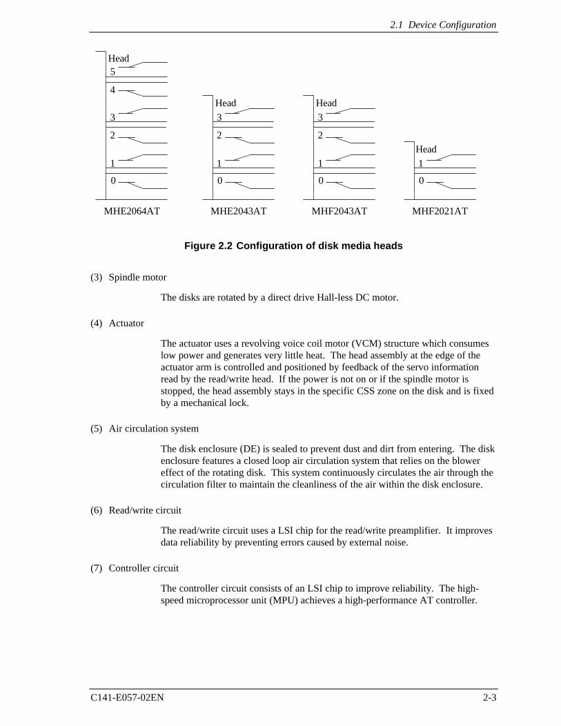
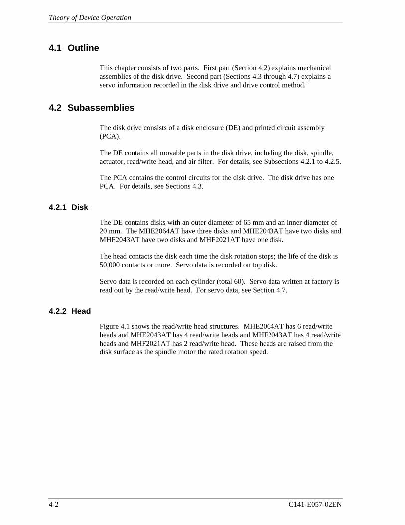
Figure 2.2 illustrates the configuration of the disks and heads of each model. Inthe disk surface, servo information necessary for controlling positioning andread/write and user data are written. Numerals 0 to 5 indicate read/write heads.
MHF20xxATMHE20xxAT
2.1 Device Configuration
C141-E057-02EN 2-3
MHE2064AT
3
4
5Head
1
2
0
MHE2043AT
3
1
2
0
MHF2043AT
3HeadHead
1
2
0
Head
MHF2021AT
1
0
Figure 2.2 Configuration of disk media heads
(3) Spindle motor
The disks are rotated by a direct drive Hall-less DC motor.
(4) Actuator
The actuator uses a revolving voice coil motor (VCM) structure which consumeslow power and generates very little heat. The head assembly at the edge of theactuator arm is controlled and positioned by feedback of the servo informationread by the read/write head. If the power is not on or if the spindle motor isstopped, the head assembly stays in the specific CSS zone on the disk and is fixedby a mechanical lock.
(5) Air circulation system
The disk enclosure (DE) is sealed to prevent dust and dirt from entering. The diskenclosure features a closed loop air circulation system that relies on the blowereffect of the rotating disk. This system continuously circulates the air through thecirculation filter to maintain the cleanliness of the air within the disk enclosure.
(6) Read/write circuit
The read/write circuit uses a LSI chip for the read/write preamplifier. It improvesdata reliability by preventing errors caused by external noise.
(7) Controller circuit
The controller circuit consists of an LSI chip to improve reliability. The high-speed microprocessor unit (MPU) achieves a high-performance AT controller.
Device Configuration
2-4 C141-E057-02EN
2.2 System Configuration
2.2.1 ATA interface
Figures 2.3 and 2.4 show the ATA interface system configuration. The drive hasa 44-pin PC AT interface connector and supports the PIO transfer at 16.6 MB/s(ATA-3, Mode 4), the DMA transfer at 16.6 MB/s (ATA-3, Multiword mode 2)and also the U-DMA at 33.3 MB/s (ATA-3, Mode 2).
2.2.2 1 drive connection
MHC2032ATMHC2040AT
Figure 2.3 1 drive system configuration
2.2.3 2 drives connection
MHC2032ATMHC2040AT
MHC2032ATMHC2040AT
(Host adaptor)
Note:
When the drive that is not conformed to ATA is connected to the disk drive aboveconfiguration, the operation is not guaranteed.
Figure 2.4 2 drives configuration
MHE2064ATMHE2043ATMHF2043ATMHF2021AT
MHE2064ATMHE2043ATMHF2043ATMHF2021AT
MHE2064ATMHE2043ATMHF2043ATMHF2021AT
2.2 System Configuration
C141-E057-01EN 2-5
HA (host adaptor) consists of address decoder, driver, and receiver.ATA is an abbreviation of “AT attachment”. The disk drive isconformed to the ATA-4 interface.At high speed data transfer (PIO mode 3, mode 4, or DMA mode 2U-DMA mode 2), occurence of ringing or crosstalk of the signallines (AT bus) between the HA and the disk drive may be a greatcause of the obstruction of system reliability. Thus, it is necessarythat the capacitance of the signal lines including the HA and cabledoes not exceed the ATA-4 standard, and the cable length betweenthe HA and the disk drive should be as short as possible.No need to push the top cover of the disk drive. If the over-powerworked, the cover could be contacted with the spindle motor. Thus,that could be made it the cause of failure.

This page is intentionally left blank.
C141-E057-01EN 3-1
CHAPTER 3 Installation Conditions
3.1 Dimensions
3.2 Mounting
3.3 Cable Connections
3.4 Jumper Settings
This chapter gives the external dimensions, installation conditions, surfacetemperature conditions, cable connections, and switch settings of the hard diskdrives.
Installation Conditions
3-2 C141-E057-01EN
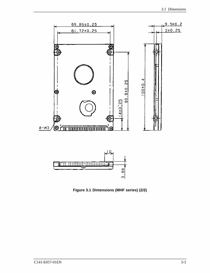
3.1 Dimensions
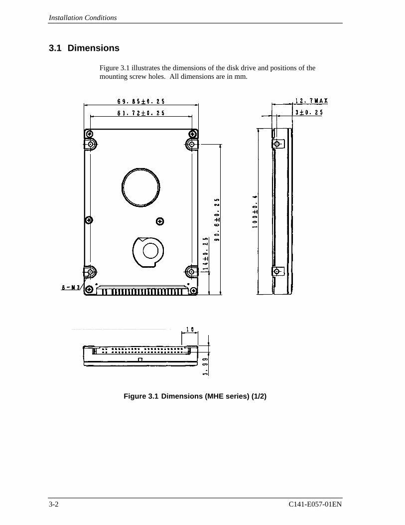
Figure 3.1 illustrates the dimensions of the disk drive and positions of themounting screw holes. All dimensions are in mm.
Figure 3.1 Dimensions (MHE series) (1/2)
3.1 Dimensions
C141-E057-01EN 3-3
Figure 3.1 Dimensions (MHF series) (2/2)
Installation Conditions
3-4 C141-E057-01EN
3.2 Mounting
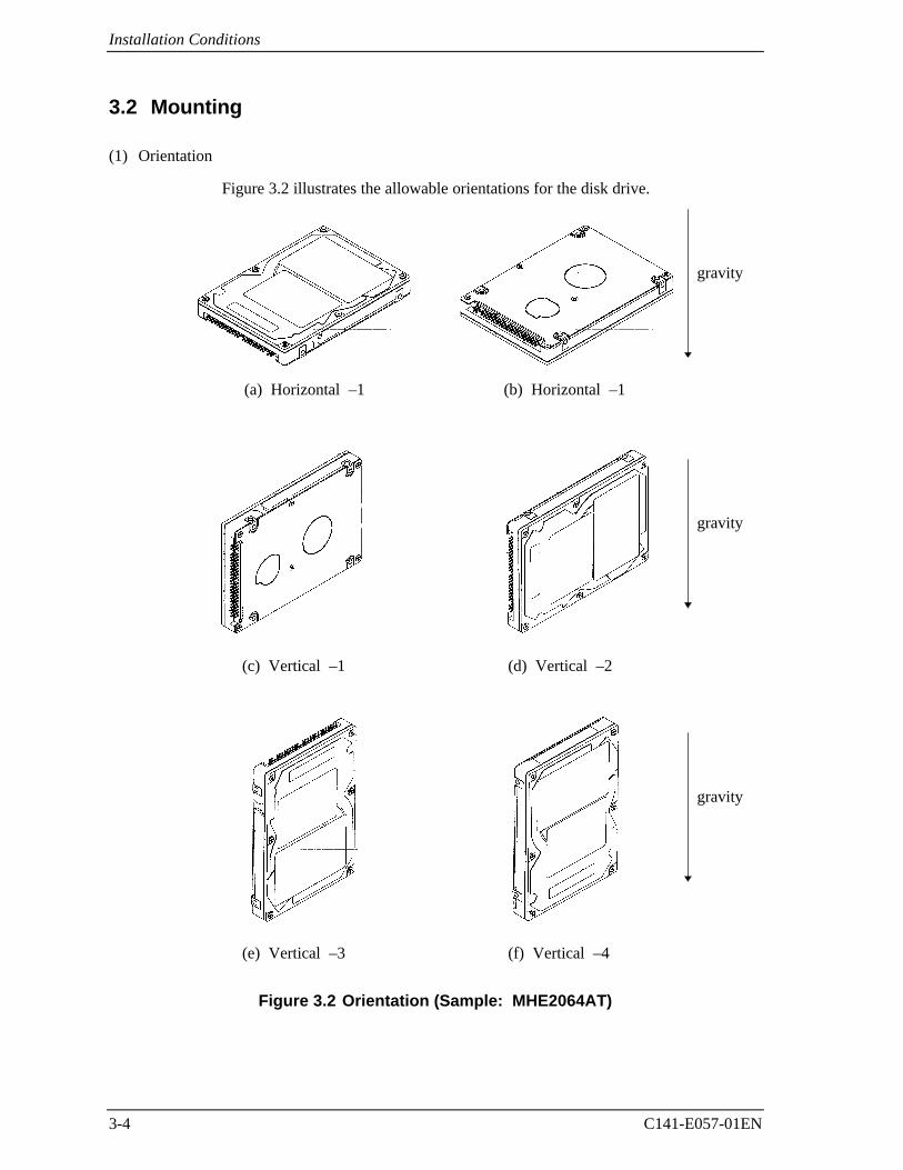
(1) Orientation
Figure 3.2 illustrates the allowable orientations for the disk drive.
Figure 3.2 Orientation (Sample: MHE2064AT)
(e) Vertical –3 (f) Vertical –4
(c) Vertical –1 (d) Vertical –2
(b) Horizontal –1(a) Horizontal –1
gravity
gravity
gravity
3.2 Mounting
C141-E057-01EN 3-5
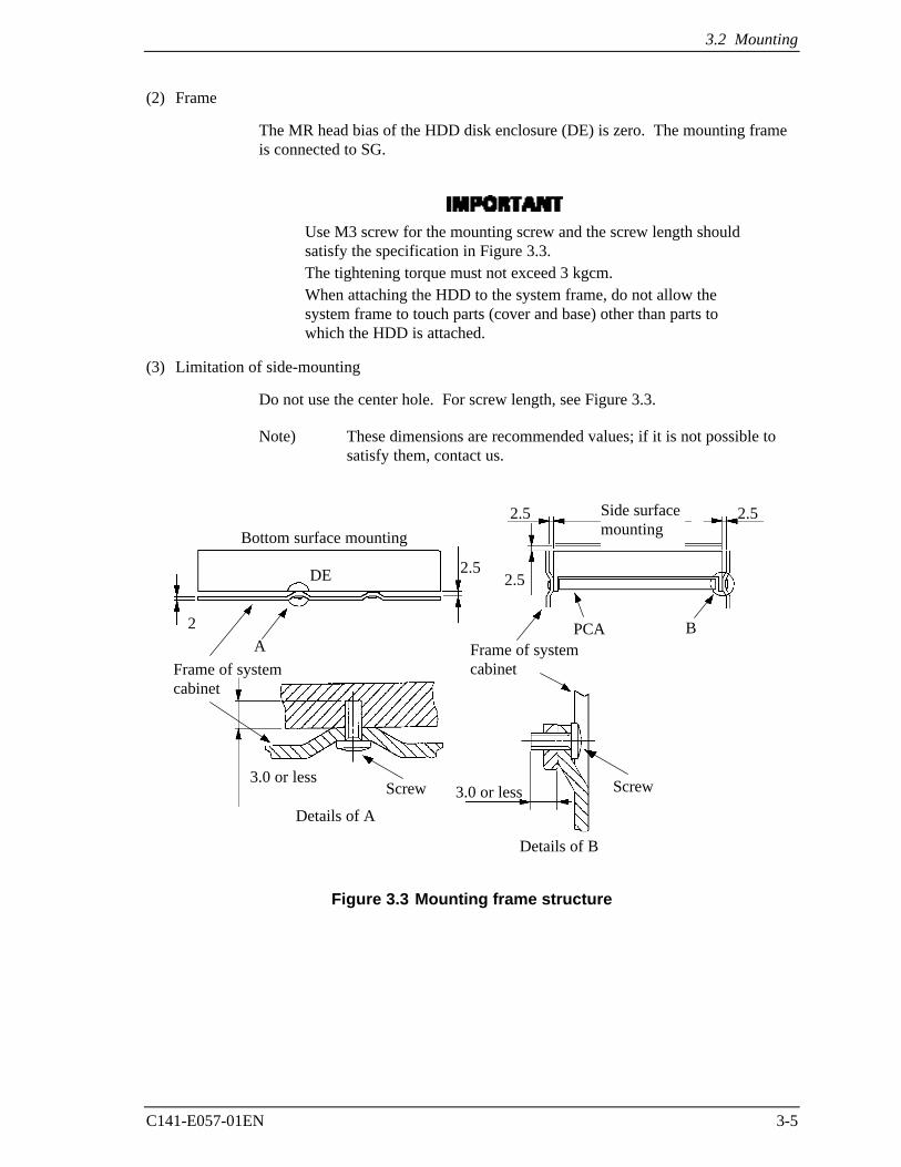
(2) Frame
The MR head bias of the HDD disk enclosure (DE) is zero. The mounting frameis connected to SG.
Use M3 screw for the mounting screw and the screw length shouldsatisfy the specification in Figure 3.3.The tightening torque must not exceed 3 kgcm.When attaching the HDD to the system frame, do not allow thesystem frame to touch parts (cover and base) other than parts towhich the HDD is attached.
(3) Limitation of side-mounting
Do not use the center hole. For screw length, see Figure 3.3.
Note) These dimensions are recommended values; if it is not possible tosatisfy them, contact us.
Figure 3.3 Mounting frame structure
ScrewScrew
Details of B
Details of A
3.0 or less3.0 or less
Frame of systemcabinetFrame of system
cabinet
BPCAA
2
2.52.5
2.52.5DE
Side surfacemountingBottom surface mounting
Installation Conditions
3-6 C141-E057-01EN
(4) Ambient temperature
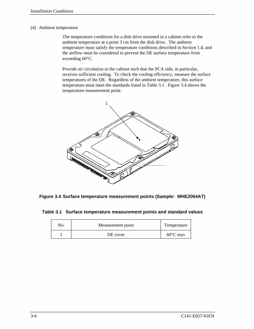
The temperature conditions for a disk drive mounted in a cabinet refer to theambient temperature at a point 3 cm from the disk drive. The ambienttemperature must satisfy the temperature conditions described in Section 1.4, andthe airflow must be considered to prevent the DE surface temperature fromexceeding 60°C.
Provide air circulation in the cabinet such that the PCA side, in particular,receives sufficient cooling. To check the cooling efficiency, measure the surfacetemperatures of the DE. Regardless of the ambient temperature, this surfacetemperature must meet the standards listed in Table 3.1. Figure 3.4 shows thetemperature measurement point.
Figure 3.4 Surface temperature measurement points (Sample: MHE2064AT)
Table 3.1 Surface temperature measurement points and standard values
No. Measurement point Temperature
1 DE cover 60°C max
1
3.2 Mounting
C141-E057-02EN 3-7
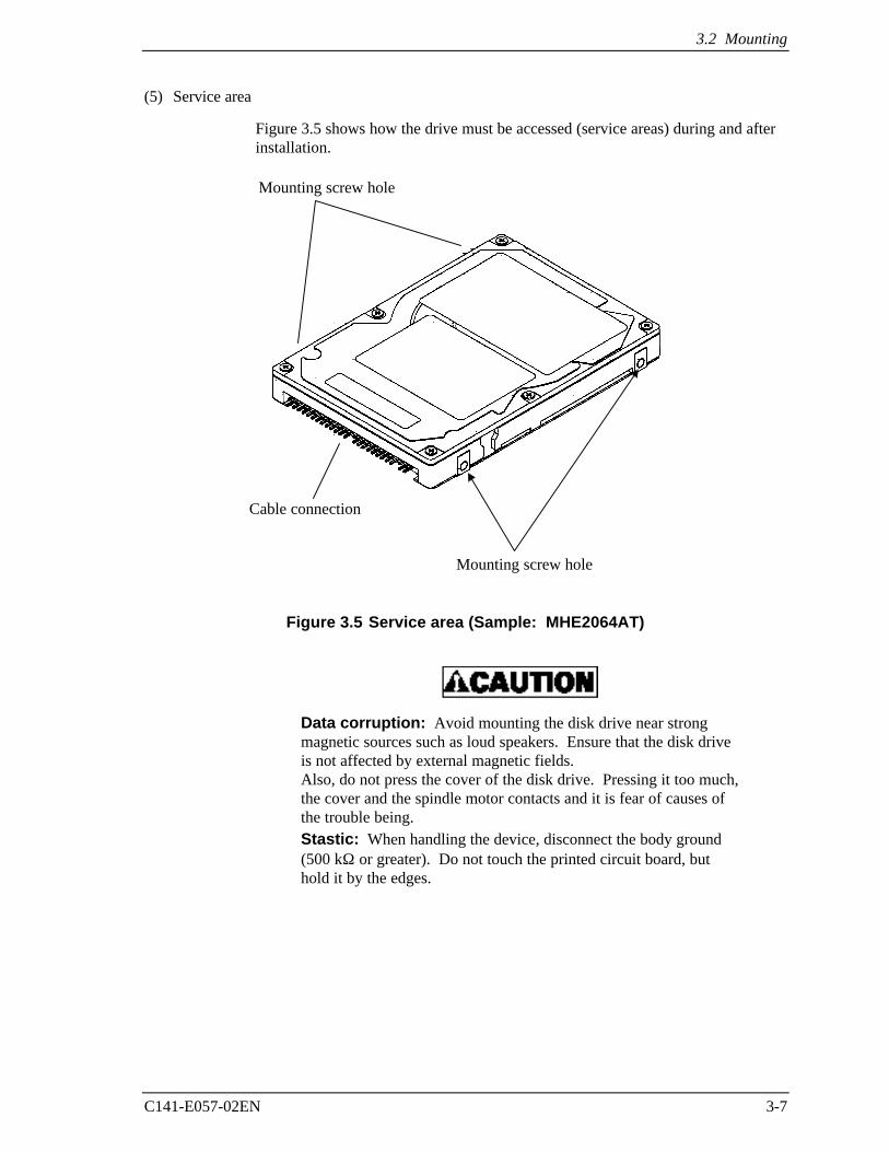
(5) Service area
Figure 3.5 shows how the drive must be accessed (service areas) during and afterinstallation.
Figure 3.5 Service area (Sample: MHE2064AT)
Data corruption: Avoid mounting the disk drive near strongmagnetic sources such as loud speakers. Ensure that the disk driveis not affected by external magnetic fields.Also, do not press the cover of the disk drive. Pressing it too much,the cover and the spindle motor contacts and it is fear of causes ofthe trouble being.Stastic: When handling the device, disconnect the body ground(500 kΩ or greater). Do not touch the printed circuit board, buthold it by the edges.
Mounting screw hole
Mounting screw hole
Cable connection
Installation Conditions
3-8 C141-E057-01EN
3.3 Cable Connections
3.3.1 Device connector
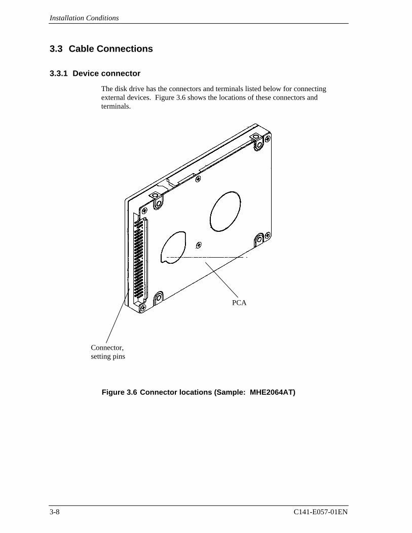
The disk drive has the connectors and terminals listed below for connectingexternal devices. Figure 3.6 shows the locations of these connectors andterminals.
Figure 3.6 Connector locations (Sample: MHE2064AT)
Connector,setting pins
PCA
3.3 Cable Connections
C141-E057-01EN 3-9
3.3.2 Cable connector specifications
Table 3.2 lists the recommended specifications for the cable connectors.
Table 3.2 Cable connector specifications
Name Model Manufacturer
ATA interface and powersupply cable (44-pin type)
Cable socket(44-pin type)
89361-144 BERG
For the host interface cable, use a ribbon cable. A twisted cable or acable with wires that have become separated from the ribbon maycause crosstalk between signal lines. This is because the interface isdesigned for ribbon cables and not for cables carrying differentialsignals.
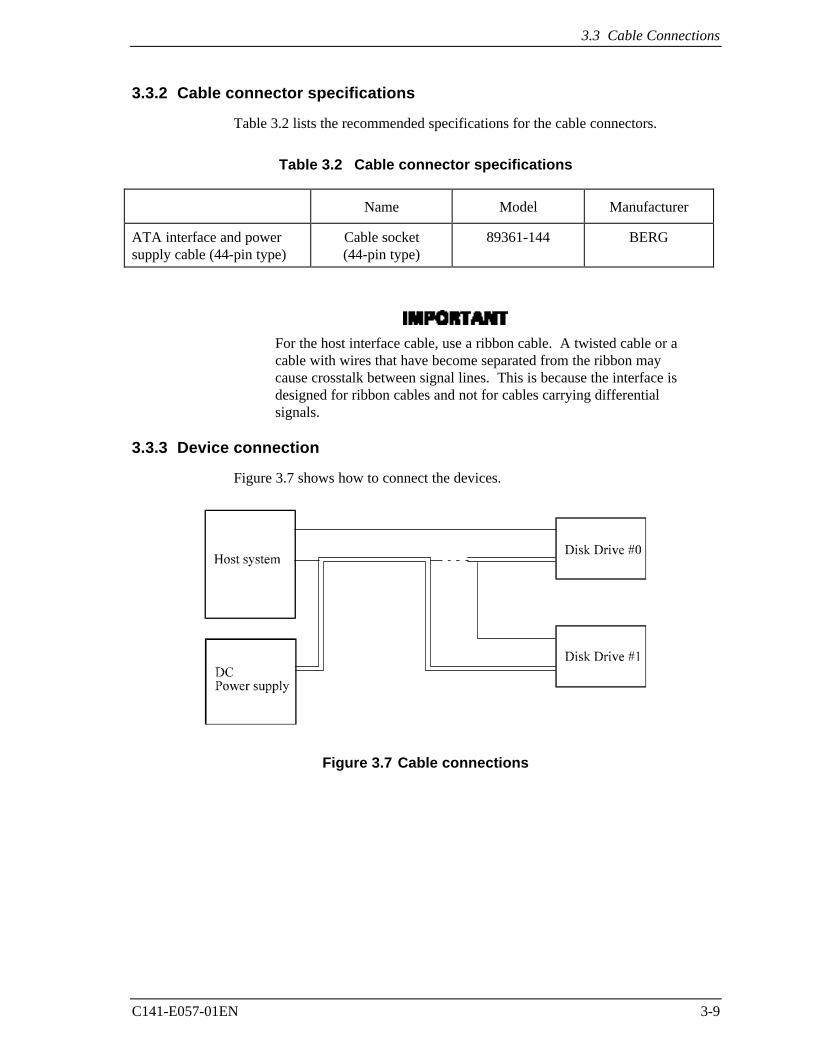
3.3.3 Device connection
Figure 3.7 shows how to connect the devices.
Figure 3.7 Cable connections
Installation Conditions
3-10 C141-E057-01EN
3.3.4 Power supply connector (CN1)
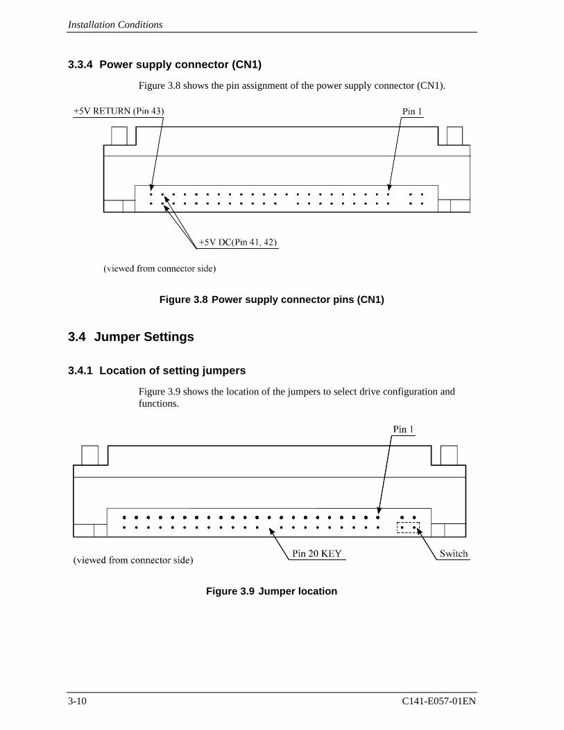
Figure 3.8 shows the pin assignment of the power supply connector (CN1).
Figure 3.8 Power supply connector pins (CN1)
3.4 Jumper Settings
3.4.1 Location of setting jumpers
Figure 3.9 shows the location of the jumpers to select drive configuration andfunctions.
Figure 3.9 Jumper location
3.4 Jumper Settings
C141-E057-02EN 3-11
3.4.2 Factory default setting
Figure 3.10 shows the default setting position at the factory.
Figure 3.10 Factory default setting
3.4.3 Master drive-slave drive setting
Master device (device #0) or slave device (device #1) is selected.
(b) Slave drive(a) Master driveOpen
Open
ShortOpen
A1 C
BD2 BD2
AC1
Figure 3.11 Jumper setting of master or slave device
Note:
Pins A and C should be open.
Open
Installation Conditions
3-12 C141-E057-02EN
3.4.4 CSEL setting
Figure 3.12 shows the cable select (CSEL) setting.
Short
Open
BD2
AC1
Note:
The CSEL setting is not depended on setting between pins Band D.
Figure 3.12 CSEL setting
Figure 3.13 and 3.14 show examples of cable selection using unique interfacecables.
By connecting the CSEL of the master device to the CSEL Line (conducer) of thecable and connecting it to ground further, the CSEL is set to low level. Thedevice is identified as a master device. At this time, the CSEL of the slave devicedoes not have a conductor. Thus, since the slave device is not connected to theCSEL conductor, the CSEL is set to high level. The device is identified as a slavedevice.
Figure 3.13 Example (1) of Cable Select
3.4 Jumper Settings
C141-E057-01EN 3-13
Figure 3.14 Example (2) of Cable Select

This page is intentionally left blank.
C141-E057-01EN 4-1
CHAPTER 4 Theory of Device Operation
4.1 Outline
4.2 Subassemblies
4.3 Circuit Configuration
4.4 Power-on Sequence
4.5 Self-calibration
4.6 Read/write Circuit
4.7 Servo Control
This chapter explains basic design concepts of the disk drive. Also, this chapterexplains subassemblies of the disk drive, each sequence, servo control, andelectrical circuit blocks.
Theory of Device Operation
4-2 C141-E057-02EN
4.1 Outline
This chapter consists of two parts. First part (Section 4.2) explains mechanicalassemblies of the disk drive. Second part (Sections 4.3 through 4.7) explains aservo information recorded in the disk drive and drive control method.
4.2 Subassemblies
The disk drive consists of a disk enclosure (DE) and printed circuit assembly(PCA).
The DE contains all movable parts in the disk drive, including the disk, spindle,actuator, read/write head, and air filter. For details, see Subsections 4.2.1 to 4.2.5.
The PCA contains the control circuits for the disk drive. The disk drive has onePCA. For details, see Sections 4.3.
4.2.1 Disk
The DE contains disks with an outer diameter of 65 mm and an inner diameter of20 mm. The MHE2064AT have three disks and MHE2043AT have two disks andMHF2043AT have two disks and MHF2021AT have one disk.
The head contacts the disk each time the disk rotation stops; the life of the disk is50,000 contacts or more. Servo data is recorded on top disk.
Servo data is recorded on each cylinder (total 60). Servo data written at factory isread out by the read/write head. For servo data, see Section 4.7.
4.2.2 Head
Figure 4.1 shows the read/write head structures. MHE2064AT has 6 read/writeheads and MHE2043AT has 4 read/write heads and MHF2043AT has 4 read/writeheads and MHF2021AT has 2 read/write head. These heads are raised from thedisk surface as the spindle motor the rated rotation speed.
4.2 Subassemblies
C141-E057-02EN 4-3
MHE2064AT
3
4
5Head
1
2
0
MHE2043AT
3
1
2
0
MHF2043AT
3HeadHead
1
2
0
Head
MHF2021AT
1
0
Figure 4.1 Head structure
4.2.3 Spindle
The spindle consists of a disk stack assembly and spindle motor. The disk stackassembly is activated by the direct drive sensor-less DC spindle motor, which hasa speed of 4,200 rpm ±1%. The spindle is controlled with detecting a PHASEsignal generated by counter electromotive voltage of the spindle motor at starting.
4.2.4 Actuator
The actuator consists of a voice coil motor (VCM) and a head carriage. The VCMmoves the head carriage along the inner or outer edge of the disk. The headcarriage position is controlled by feeding back the difference of the target positionthat is detected and reproduced from the servo information read by the read/writehead.
4.2.5 Air filter
There are two types of air filters: a breather filter and a circulation filter.
The breather filter makes an air in and out of the DE to prevent unnecessarypressure around the spindle when the disk starts or stops rotating. When diskdrives are transported under conditions where the air pressure changes a lot,filtered air is circulated in the DE.
The circulation filter cleans out dust and dirt from inside the DE. The disk drivecycles air continuously through the circulation filter through an enclosed loop aircycle system operated by a blower on the rotating disk.
Theory of Device Operation
4-4 C141-E057-01EN
4.3 Circuit Configuration
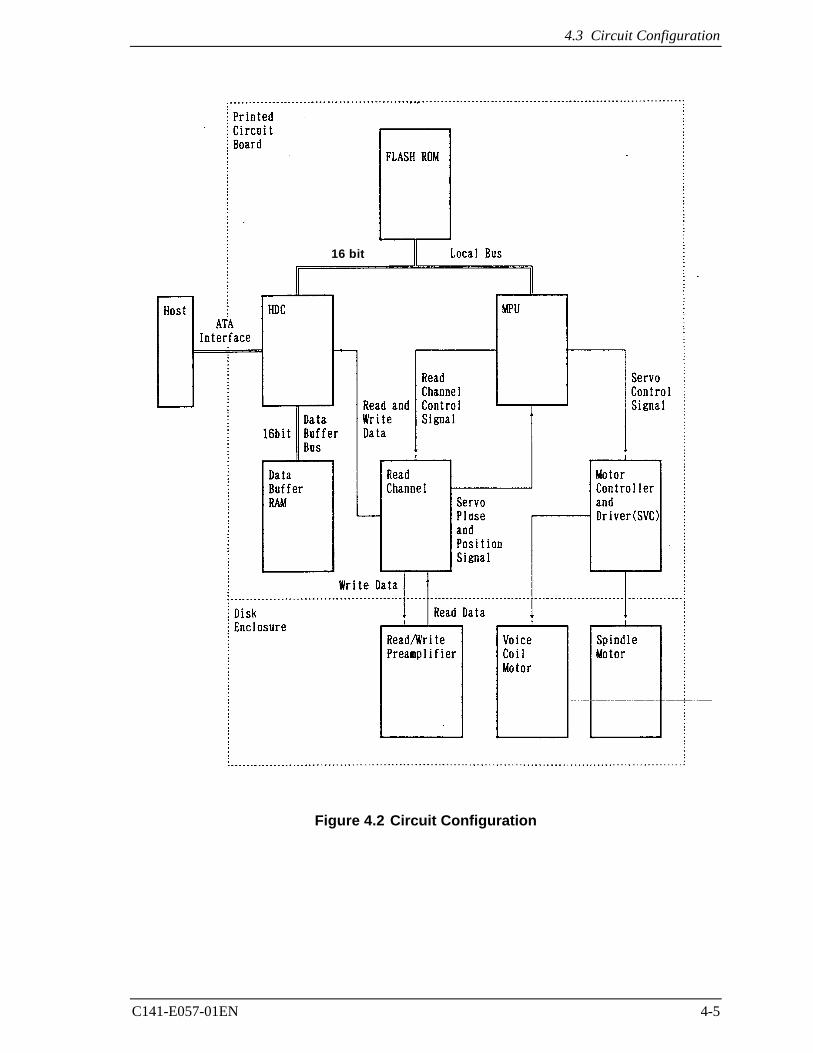
Figure 4.2 shows the disk drive circuit configuration.
(1) Read/write circuit
The read/write circuit consists of two LSIs; read/write preamplifier (PreAMP) andread channel (RDC).
The PreAMP consists of the write current switch circuit, that flows the writecurrent to the head coil, and the voltage amplifier circuit, that amplitudes the readoutput from the head.
The RDC is the read demodulation circuit using the extended partial responseclass 4 (EPR4), and contains the Viterbi detector, programmable filter, adaptabletransversal filter, times base generator, and data separator circuits. The RDC alsocontains the 16/17 group coded recording (GCR) encoder and decoder and servodemodulation circuit.
(2) Servo circuit
The position and speed of the voice coil motor are controlled by 2 closed-loopservo using the servo information recorded on the data surface. The servoinformation is an analog signal converted to digital for processeing by a MPU andthen reconverted to an analog signal for control of the voice coil motor.
The MPU precisely sets each head on the track according on the servo informationon the media surface.
(3) Spindle motor driver circuit
The circuit measures the interval of a PHASE signal generated by counter-electromotive voltage of a motor at the MPU and controls the motor speedcomparing target speed.
(4) Controller circuit
Major functions are listed below.
• Data buffer (512 KB) management
• ATA interface control and data transfer control
• Sector format control
• Defect management
• ECC control
• Error recovery and self-diagnosis
4.3 Circuit Configuration
C141-E057-01EN 4-5
Figure 4.2 Circuit Configuration
16 bit
Theory of Device Operation
4-6 C141-E057-01EN
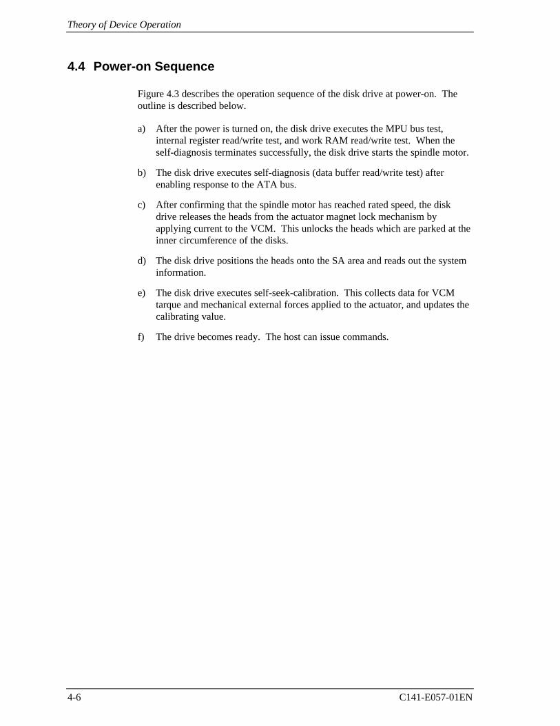
4.4 Power-on Sequence
Figure 4.3 describes the operation sequence of the disk drive at power-on. Theoutline is described below.
a) After the power is turned on, the disk drive executes the MPU bus test,internal register read/write test, and work RAM read/write test. When theself-diagnosis terminates successfully, the disk drive starts the spindle motor.
b) The disk drive executes self-diagnosis (data buffer read/write test) afterenabling response to the ATA bus.
c) After confirming that the spindle motor has reached rated speed, the diskdrive releases the heads from the actuator magnet lock mechanism byapplying current to the VCM. This unlocks the heads which are parked at theinner circumference of the disks.
d) The disk drive positions the heads onto the SA area and reads out the systeminformation.
e) The disk drive executes self-seek-calibration. This collects data for VCMtarque and mechanical external forces applied to the actuator, and updates thecalibrating value.
f) The drive becomes ready. The host can issue commands.
4.5 Self-calibration
C141-E057-01EN 4-7
Figure 4.3 Power-on operation sequence
4.5 Self-calibration
The disk drive occasionally performs self-calibration in order to sense andcalibrate mechanical external forces on the actuator, and VCM tarque. Thisenables precise seek and read/write operations.
4.5.1 Self-calibration contents
(1) Sensing and compensating for external forces
The actuator suffers from torque due to the FPC forces and winds accompanyingdisk revolution. The torque vary with the disk drive and the cylinder where thehead is positioned. To execute stable fast seek operations, external forces areoccasionally sensed.
The firmware of the drive measures and stores the force (value of the actuatormotor drive current) that balances the torque for stopping head stably. Thisincludes the current offset in the power amplifier circuit and DAC system.
Theory of Device Operation
4-8 C141-E057-01EN
The forces are compensated by adding the measured value to the specified currentvalue to the power amplifier. This makes the stable servo control.
To compensate torque varing by the cylinder, the disk is divided into 8 areas fromthe innermost to the outermost circumference and the compensating value ismeasured at the measuring cylinder on each area at factory calibration. Themeasured values are stored in the SA cylinder. In the self-calibration, thecompensating value is updated using the value in the SA cylinder.
(2) Compensating open loop gain
Torque constant value of the VCM has a dispersion for each drive, and variesdepending on the cylinder that the head is positioned. To realize the high speedseek operation, the value that compensates torque constant value change and loopgain change of the whole servo system due to temperature change is measured andstored.
For sensing, the firmware mixes the disturbance signal to the position signal at thestate that the head is positioned to any cylinder. The firmware calculates the loopgain from the position signal and stores the compensation value against to thetarget gain as ratio.
For compensating, the direction current value to the power amplifier is multipliedby the compensation value. By this compensation, loop gain becomes constantvalue and the stable servo control is realized.
To compensate torque constant value change depending on cylinder, wholecylinders from most inner to most outer cylinder are divided into 8 partitions atcalibration in the factory, and the compensation data is measured for representivecylinder of each partition. This measured value is stored in the SA area. Thecompensation value at self-calibration is calculated using the value in the SA area.
4.5.2 Execution timing of self-calibration
Self-calibration is executed when:
• The power is turned on.
• The disk drive receives the RECALIBRATE command from the host.
• The self-calibration execution timechart of the disk drive specifies self-calibration.
The disk drive performs self-calibration according to the timechart based on thetime elapsed from power-on. The timechart is shown in Table 4.1. After power-on, self-calibration is performed about every five or ten or fifteen minutes for thefirst 60 minutes or six RECALIBRATE command executions, and about every 30minutes after that.
4.6 Read/write Circuit
C141-E057-01EN 4-9
Table 4.1 Self-calibration execution timechart
Time elapsed Time elapsed(accumulated)
1 At power-on Initial calibration
2 About 5 minutes About 5 minutes
3 About 5 minutes About 10 minutes
4 About 10 minutes About 20 minutes
5 About 10 minutes About 30 minutes
6 About 15 minutes About 45 minutes
7 About 15 minutes About 60 minutes
8....
Every about 30minutes
4.5.3 Command processing during self-calibration
If the disk drive receives a command execution request from the host whileexecuting self-calibration according to the timechart, the disk drive terminatesself-calibration and starts executing the command precedingly. In other words, ifa disk read or write service is necessary, the disk drive positions the head to thetrack requested by the host, reads or writes data, and restarts calibration.
This enables the host to execute the command without waiting for a long time,even when the disk drive is performing self-calibration. The command executionwait time is about maximum 100 ms.
4.6 Read/write Circuit
The read/write circuit consists of the read/write preamplifier (PreAMP), the writecircuit, the read circuit, and the time base generator in the read channel (RDC).Figure 4.4 is a block diagram of the read/write circuit.
4.6.1 Read/write preamplifier (PreAMP)
One PreAMP is mounted on the FPC. The PreAMP consists of an readpreamplifier and a write current switch and senses a write error. Each channel isconnected to each data head. The head IC switches the heads by the chip selectsignals (*CS) and the head select signals. The IC generates a write error sense
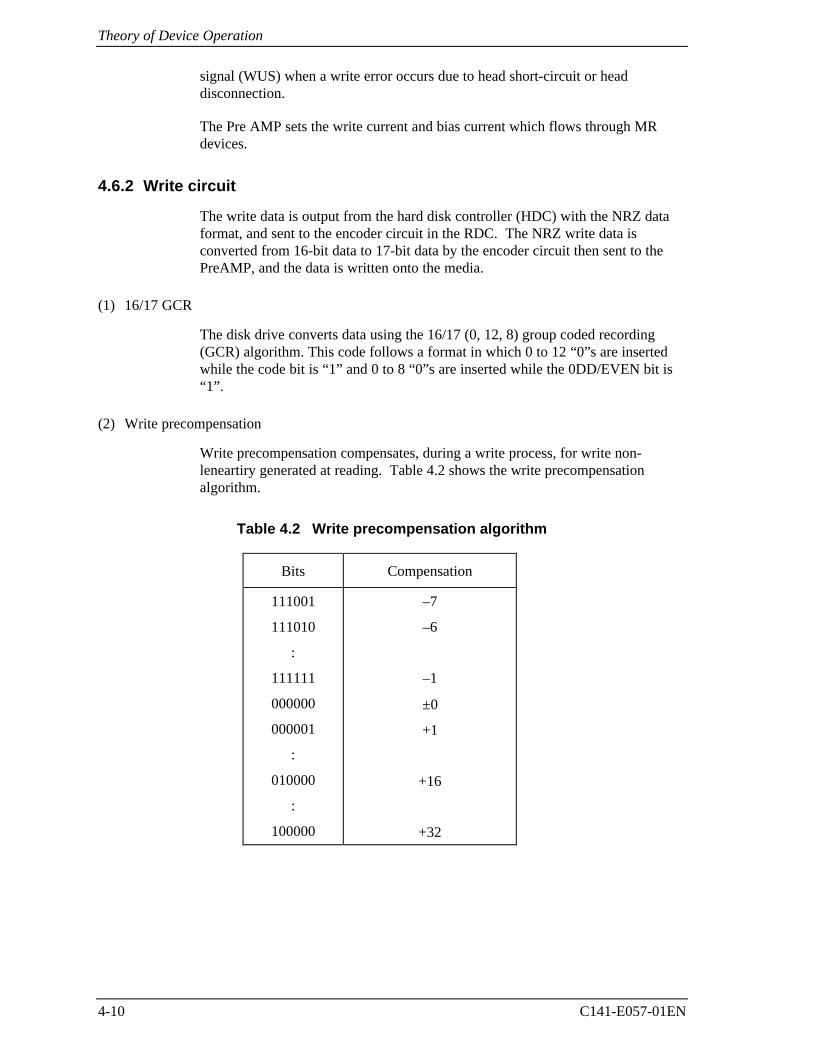
Theory of Device Operation
4-10 C141-E057-01EN
signal (WUS) when a write error occurs due to head short-circuit or headdisconnection.
The Pre AMP sets the write current and bias current which flows through MRdevices.
4.6.2 Write circuit
The write data is output from the hard disk controller (HDC) with the NRZ dataformat, and sent to the encoder circuit in the RDC. The NRZ write data isconverted from 16-bit data to 17-bit data by the encoder circuit then sent to thePreAMP, and the data is written onto the media.
(1) 16/17 GCR
The disk drive converts data using the 16/17 (0, 12, 8) group coded recording(GCR) algorithm. This code follows a format in which 0 to 12 “0”s are insertedwhile the code bit is “1” and 0 to 8 “0”s are inserted while the 0DD/EVEN bit is“1”.
(2) Write precompensation
Write precompensation compensates, during a write process, for write non-leneartiry generated at reading. Table 4.2 shows the write precompensationalgorithm.
Table 4.2 Write precompensation algorithm
Bits Compensation
111001
111010
:
111111
000000
000001
:
010000
:
100000
–7
–6
–1
±0
+1
+16
+32
4.6 Read/write Circuit
C141-E057-01EN 4-11
Figure 4.4 Read/write circuit block diagram
Theory of Device Operation
4-12 C141-E057-01EN
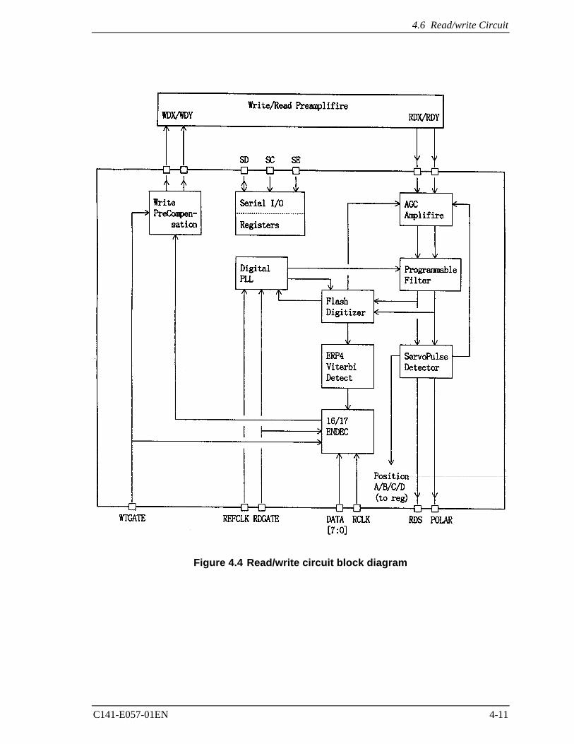
4.6.3 Read circuit
The head read signal from the PreAMP is regulated by the automatic gain control(AGC) circuit. Then the output is converted into the sampled read data pulse bythe programmable filter circuit and the flash digitizer circuit. This clock signal isconverted into the NRZ data by the 16/17 GCR decoder circuit based on the readdata maximum-likelihood-detected by the Viterbi detection circuit, then is sent tothe HDC.
(1) AGC circuit
The AGC circuit automatically regulates the output amplitude to a constant valueeven when the input amplitude level fluctuates. The AGC amplifier output ismaintained at a constant level even when the head output fluctuates due to thehead characteristics or outer/inner head positions.
(2) Programmable filter
The programmable filter circuit has a low-pass filter function that eliminatesunnecessary high frequency noise component and a high frequency boost-upfunction that equalizes the waveform of the read signal.
Cut-off frequency of the low-pass filter and boost-up gain are controlled from theregister in read channel by an instruction of the serial data signal from MPU (M5).The MPU optimizes the cut-off frequency and boost-up gain according to thetransfer frequency of each zone.
Figure 4.5 shows the frequency characteristic sample of the programmalbe filter.
Figure 4.5 Frequency characteristic of programmable filter
-3 dB
4.6 Read/write Circuit
C141-E057-01EN 4-13
(3) Flash digitizer circuit
This circuit is 10-tap sampled analog transversal filter circuit that cosine-equalizesthe head read signal to the partial response class 4 (EPR4) waveform.
(4) Viterbi detection circuit
The sample hold waveform output from the flash digitizer circuit is sent to theViterbi detection circuit. The Viterbi detection circuit demodulates data accordingto the survivor path sequence.
(5) 16/17 GCR decoder
This circuit converts the 17-bit read data into the 16-bit NRZ data.
4.6.4 Digital PLL circuit
The drive uses constant density recording to increase total capacity. This isdifferent from the conventional method of recording data with a fixed data transferrate at all data area. In the constant density recording method, data area is dividedinto zones by radius and the data transfer rate is set so that the recording densityof the inner cylinder of each zone is nearly constant. The drive divides data areainto 14 zones to set the data transfer rate.
The MPU transfers the data transfer rate setup data (SD/SC) to the RDC thatincludes the Digital PLL circuit to change the data transfer rate.
Theory of Device Operation
4-14 C141-E057-01EN
4.7 Servo Control
The actuator motor and the spindle motor are submitted to servo control. Theactuator motor is controlled for moving and positioning the head to the trackcontaining the desired data. To turn the disk at a constant velocity, the actuatormotor is controlled according to the servo data that is written on the data sidebeforehand.
4.7.1 Servo control circuit
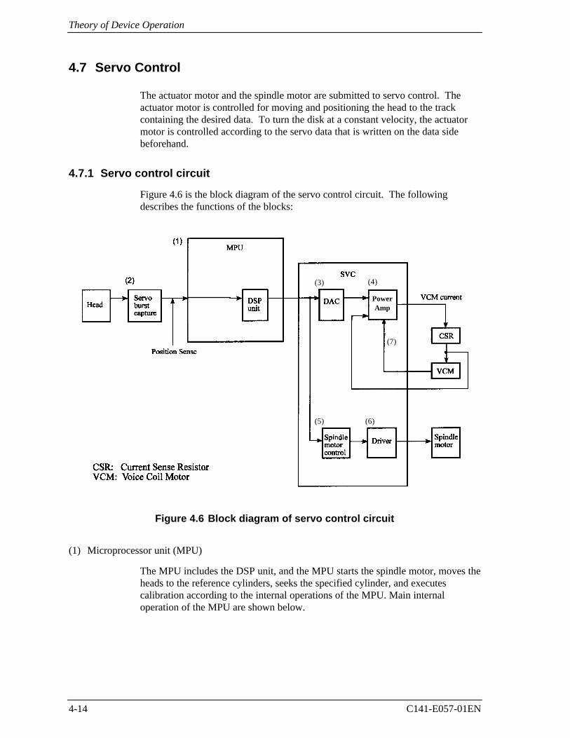
Figure 4.6 is the block diagram of the servo control circuit. The followingdescribes the functions of the blocks:
Figure 4.6 Block diagram of servo control circuit
(1) Microprocessor unit (MPU)
The MPU includes the DSP unit, and the MPU starts the spindle motor, moves theheads to the reference cylinders, seeks the specified cylinder, and executescalibration according to the internal operations of the MPU. Main internaloperation of the MPU are shown below.
(6)(5)
(7)
(4)(3)
PowerAmp
4.7 Servo Control
C141-E057-01EN 4-15
The major internal operations are listed below.
a. Spindle motor start
Starts the spindle motor and accelerates it to normal speed when power isapplied.
b. Move head to reference cylinder
Drives the VCM to position the head at the any cylinder in the data area. Thelogical initial cylinder is at the outermost circumference (cylinder 0).
c. Seek to specified cylinder
Drives the VCM to position the head to the specified cylinder.
d. Calibration
Senses and stores the thermal offset between heads and the mechanical forceson the actuator, and stores the calibration value.
Theory of Device Operation
4-16 C141-E057-01EN
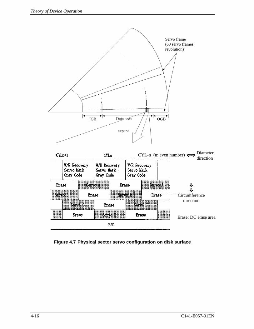
Figure 4.7 Physical sector servo configuration on disk surface
Servo frame(60 servo framesrevolution)
Circumferencedirection
Diameterdirection
Erase: DC erase area
CYL-n (n: even number)
4.7 Servo Control
C141-E057-01EN 4-17
(2) Servo burst capture circuit
The servo burst capture circuit reproduces signals (position signals) that indicatethe head position from the servo data on the data surface. SERVO A, SERVO B,SERVO C and SERVO D burst signals shown in Figure 4.8 followed the servomark, cylinder gray and index information are output from the servo area on thedata surface via the data head. The servo signals A/D-converts the amplitudes ofthe POSA, POSB, POSC and POSD signals at the peak hold circuit in the servoburst capture circuit at the timing of the STROB signal. At that time the AGCcircuit is in hold mode. The A/D converted data is recognized by the MPU asposition information with A-B and C-D processed.
(3) D/A converter (DAC)
The D/A converter (DAC) converts the VCM drive current value (digital value)calculated by the DSP unit into analog values and transfers them to the poweramplifier.
(4) Power amplifier
The power amplifier feeds currents, corresponding to the DAC output signalvoltage to the VCM.
(5) Spindle motor control circuit
The spindle motor control circuit controls the sensor-less spindle motor. Thiscircuit detects number of revolution of the motor by the interrupt generatedperiodically, compares with the target revolution speed, then flows the current intothe motor coil according to the differentation (abberration).
(6) Driver circuit
The driver circuit is a power amplitude circuit that receives signals from thespindle motor control circuit and feeds currents to the spindle motor.
(7) VCM current sense resistor (CSR)
This resistor controls current at the power amplifier by converting the VCMcurrent into voltage and feeding back.
Theory of Device Operation
4-18 C141-E057-01EN
4.7.2 Data-surface servo format
Figure 4.7 describes the physical layout of the servo frame. The three areasindicated by (1) to (3) in Figure 4.7 are described below.
(1) Inner guard band
The head is in contact with the disk in this space when the spindle starts turning orstops, and the rotational speed of the spindle can be controlled on this cylinderarea for head moving.
(2) Data area
This area is used as the user data area SA area.
(3) Outer guard band
This area is located at outer position of the user data area, and the rotational speedof the spindle can be controlled on this cylinder area for head moving.
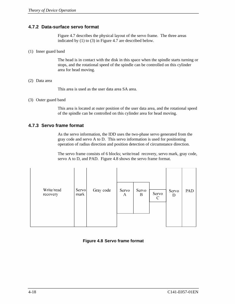
4.7.3 Servo frame format
As the servo information, the IDD uses the two-phase servo generated from thegray code and servo A to D. This servo information is used for positioningoperation of radius direction and position detection of circumstance direction.
The servo frame consists of 6 blocks; write/read recovery, servo mark, gray code,servo A to D, and PAD. Figure 4.8 shows the servo frame format.
Figure 4.8 Servo frame format
4.7 Servo Control
C141-E057-01EN 4-19
(1) Write/read recovery
This area is used to absorb the write/read transient and to stabilize the AGC.
(2) Servo mark
This area gererates a timing for demodulating the gray code and position-demodulating the servo A to D by detecting the servo mark.
(3) Gray code (including index bit)
This area is used as cylinder address. The data in this area is converted into thebinary data by the gray code demodulation circuit
(4) Servo A, servo B, servo C, servo D
This area is used as position signals between tracks, and the IDD control at on-track so that servo A level equals to servo B level.
(5) PAD
This area is used as a gap between servo and data.
4.7.4 Actuator motor control
The voice coil motor (VCM) is controlled by feeding back the servo data recordedon the data surface. The MPU fetches the position sense data on the servo frameat a constant interval of sampling time, executes calculation, and updates theVCM drive current.
The servo control of the actuator includes the operation to move the head to thereference cylinder, the seek operation to move the head to the target cylinder toread or write data, and the track-following operation to position the head onto thetarget track.
(1) Operation to move the head to the reference cylinder
The MPU moves the head to the reference cylinder when the power is turned. Thereference cylinder is in the data area.
When power is applied the heads are moved from the inner circumference shuntzone to the normal servo data zone in the following sequence:
a) Micro current is fed to the VCM to press the head against the innercircumference.
b) Micro current is fed to the VCM to move the head toward the outercircumference.
c) When the servo mark is detected the head is moved slowly toward the outercircumference at a constant speed.
Theory of Device Operation
4-20 C141-E057-01EN
d) If the head is stopped at the reference cylinder from there. Track followingcontrol starts.
(2) Seek operation
Upon a data read/write request from the host, the MPU confirms the necessity ofaccess to the disk. If a read/write instruction is issued, the MPU seeks the desiredtrack.
The MPU feeds the VCM current via the D/A converter and power amplifier tomove the head. The MPU calculates the difference (speed error) between thespecified target position and the current position for each sampling timing duringhead moving. The MPU then feeds the VCM drive current by setting thecalculated result into the D/A converter. The calculation is digitally executed bythe firmware. When the head arrives at the target cylinder, the track is followed.
(3) Track following operation
Except during head movement to the reference cylinder and seek operation underthe spindle rotates in steady speed, the MPU does track following control. Toposition the head at the center of a track, the DSP drives the VCM by feedingmicro current. For each sampling time, the VCM drive current is determined byfiltering the position difference between the target position and the positionclarified by the detected position sense data. The filtering includes servocompensation. These are digitally controlled by the firmware.
4.7.5 Spindle motor control
Hall-less three-phase twelve-pole motor is used for the spindle motor, and the 3-phase full/half-wave analog current control circuit is used as the spindle motordriver (called SVC hereafter). The firmware operates on the MPU manufacturedby Fujitsu. The spindle motor is controlled by sending several signals from theMPU to the SVC. There are three modes for the spindle control; start mode,acceleration mode, and stable rotation mode.
(1) Start mode
When power is supplied, the spindle motor is started in the following sequence:
a) After the power is turned on, the MPU sends a signal to the SVC to chargethe charge pump capacitor of the SVC. The charged amount defines thecurrent that flows in the spindle motor.
b) When the charge pump capacitor is charged enough, the MPU sets the SVCto the motor start mode. Then, a current (approx. 0.7 A) flows into thespindle motor.
c) The SVC generates a phase switching signal by itself, and changes the phaseof the current flowed in the motor in the order of (V-phase to U-phase), (W-phase to U-phase), (W-phase to V-phase), (U-phase to V-phase), (U-phase toW-phase), and (V-phase to W-phase) (after that, repeating this order).
4.7 Servo Control
C141-E057-01EN 4-21
d) During phase switching, the spindle motor starts rotating in low speed, andgenerates a counter electromotive force. The SVC detects this counterelectromotive force and reports to the MPU using a PHASE signal for speeddetection.
e) The MPU is waiting for a PHASE signal. When no phase signal is sent for asepcific period, the MPU resets the SVC and starts from the beginning.When a PHASE signal is sent, the SVC enters the acceleration mode.
(2) Acceleration mode
In this mode, the MPU stops to send the phase switching signal to the SVC. TheSVC starts a phase switching by itself based on the counter electromotive force.Then, rotation of the spindle motor accelerates. The MPU calcurates a rotationalspeed of the spindle motor based on the PHASE signal from the SVC, andaccelerates till the rotational speed reaches 4,200 rpm. When the rotational speedreaches 4,200 rpm, the SVC enters the stable rotation mode.
(3) Stable rotation mode
The MPU calcurates a time for one revolution of the spindle motor based on thePHASE signal from the SVC. The MPU takes a difference between the currenttime and a time for one revolution at 4,200 rpm that the MPU already recognized.Then, the MPU keeps the rotational speed to 4,200 rpm by charging ordischarging the charge pump for the different time. For example, when the actualrotational speed is 4,000 rpm, the time for one revolution is 15.000 ms. And, thetime for one revolution at 4,200 rpm is 14.286 ms. Therefore, the MPU chargesthe charge pump for 0.714 ms × k (k: constant value). This makes the flowedcurrent into the motor higher and the rotational speed up. When the actualrotational speed is faster than 4,200 rpm, the MPU discharges the pump the otherway. This control (charging/discharging) is performed every 1 revolution.

This page is intentionally left blank.
C141-E057-01EN 5-1
CHAPTER 5 Interface
5.1 Physical Interface
5.2 Logical Interface
5.3 Host Commands
5.4 Command Protocol
5.5 Ultra DMA Feature Set
5.6 Timing
This chapter gives details about the interface, and the interface commands andtimings.
Interface
5-2 C141-E057-01EN
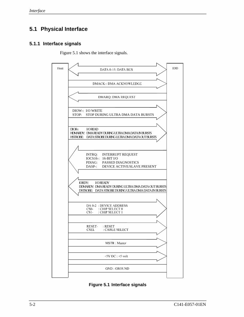
5.1 Physical Interface
5.1.1 Interface signals
Figure 5.1 shows the interface signals.
INTRQ: INTERRUPT REQUESTIOCS16-: 16-BIT I/OPDIAG: PASSED DIAGNOSTICSDASP-: DEVICE ACTIVE/SLAVE PRESENT
DIOW-: I/O WRITESTOP: STOP DURING ULTRA DMA DATA BURSTS
DIOR-: I/O READHDMARDY: DMA READY DURING ULTRA DMA DATA IN BURSTSHSTROBE: DATA STROBE DURING ULTRA DMA DATA OUT BURSTS
IORDY: I/O READYDDMARDY: DMA READY DURING ULTRA DMA DATA OUT BURSTSDSTROBE: DATA STROBE DURING ULTRA DMA DATA IN BURSTS
Figure 5.1 Interface signals
5.1 Physical Interface
C141-E057-01EN 5-3
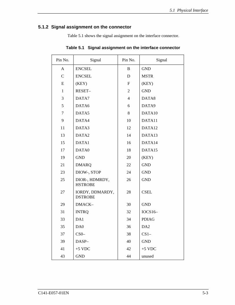
5.1.2 Signal assignment on the connector
Table 5.1 shows the signal assignment on the interface connector.
Table 5.1 Signal assignment on the interface connector
Pin No. Signal Pin No. Signal
A
C
E
1
3
5
7
9
11
13
15
17
19
21
23
25
27
29
31
33
35
37
39
41
43
ENCSEL
ENCSEL
(KEY)
RESET–
DATA7
DATA6
DATA5
DATA4
DATA3
DATA2
DATA1
DATA0
GND
DMARQ
DIOW-, STOP
DIOR-, HDMRDY,HSTROBE
IORDY, DDMARDY,DSTROBE
DMACK–
INTRQ
DA1
DA0
CS0–
DASP–
+5 VDC
GND
B
D
F
2
4
6
8
10
12
14
16
18
20
22
24
26
28
30
32
34
36
38
40
42
44
GND
MSTR
(KEY)
GND
DATA8
DATA9
DATA10
DATA11
DATA12
DATA13
DATA14
DATA15
(KEY)
GND
GND
GND
CSEL
GND
IOCS16–
PDIAG
DA2
CS1–
GND
+5 VDC
unused
Interface
5-4 C141-E057-01EN
[signal] [I/O] [Description]
ENCSEL I This signal is used to set master/slave using the CSEL signal (pin 28).
Pins A and C Open: Sets master/slave by the MSTR signalwithout using the CSEL signal.
Short: Sets master/slave using the CSEL signal.
The MSTR signal is ignored.
MSTR I MSTR, I, Master/slave setting
1: Master 0: Slave
RESET- I Reset signal from the host. This signal is low active and isasserted for a minimum of 25 µs during power on.
DATA 0-15 I/O Sixteen-bit bi-directional data bus between the host and thedevice. These signals are used for data transfer
DIOW- I Signal asserted by the host to write to the device register or dataport.
STOP I DIOW- must be negated by the host before starting the UltraDMA transfer. The STOP signal must be negated by the hostbefore data is transferred during the Ultra DMA transfer. Duringdata transfer in Ultra DMA mode, the assertion of the STOPsignal asserted by the host later indicates that the transfer has beensuspended.
DIOR- I Read strobe signal from the host to read the device register or dataport
HDMARDY- I Flow control signal for Ultra DMA data In transfer (READ DMAcommand). This signal is asserted by the host to inform thedevice that the host is ready to receive the Ultra DMA data Intransfer. The host can negate the HDMARDY- signal to suspendthe Ultra DMA data In transfer.
HSTROBE I Data Out Strobe signal from the host during Ultra DMA data Outtransfer (WRITE DMA command). Both the rising and fallingedges of the HSTROBE signal latch data from Data 15-0 into thedevice. The host can suspend the inversion of the HSTROBEsignal to suspend the Ultra DMA data Out transfer.
INTRQ O Interrupt signal to the host.
This signal is negated in the following cases:
− assertion of RESET- signal
− Reset by SRST of the Device Control register
− Write to the command register by the host
− Read of the status register by the host
− Completion of sector data transfer
(without reading the Status register)
The signal output line has a high impedance when no devices areselected or interruption is disabled.
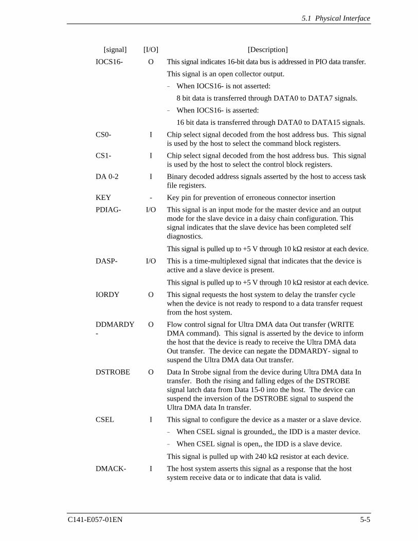
5.1 Physical Interface
C141-E057-01EN 5-5
[signal] [I/O] [Description]
IOCS16- O This signal indicates 16-bit data bus is addressed in PIO data transfer.
This signal is an open collector output.
− When IOCS16- is not asserted:
8 bit data is transferred through DATA0 to DATA7 signals.
− When IOCS16- is asserted:
16 bit data is transferred through DATA0 to DATA15 signals.
CS0- I Chip select signal decoded from the host address bus. This signalis used by the host to select the command block registers.
CS1- I Chip select signal decoded from the host address bus. This signalis used by the host to select the control block registers.
DA 0-2 I Binary decoded address signals asserted by the host to access taskfile registers.
KEY - Key pin for prevention of erroneous connector insertion
PDIAG- I/O This signal is an input mode for the master device and an outputmode for the slave device in a daisy chain configuration. Thissignal indicates that the slave device has been completed selfdiagnostics.
This signal is pulled up to +5 V through 10 kΩ resistor at each device.
DASP- I/O This is a time-multiplexed signal that indicates that the device isactive and a slave device is present.
This signal is pulled up to +5 V through 10 kΩ resistor at each device.
IORDY O This signal requests the host system to delay the transfer cyclewhen the device is not ready to respond to a data transfer requestfrom the host system.
DDMARDY-
O Flow control signal for Ultra DMA data Out transfer (WRITEDMA command). This signal is asserted by the device to informthe host that the device is ready to receive the Ultra DMA dataOut transfer. The device can negate the DDMARDY- signal tosuspend the Ultra DMA data Out transfer.
DSTROBE O Data In Strobe signal from the device during Ultra DMA data Intransfer. Both the rising and falling edges of the DSTROBEsignal latch data from Data 15-0 into the host. The device cansuspend the inversion of the DSTROBE signal to suspend theUltra DMA data In transfer.
CSEL I This signal to configure the device as a master or a slave device.
− When CSEL signal is grounded,, the IDD is a master device.
− When CSEL signal is open,, the IDD is a slave device.
This signal is pulled up with 240 kΩ resistor at each device.
DMACK- I The host system asserts this signal as a response that the hostsystem receive data or to indicate that data is valid.
Interface
5-6 C141-E057-01EN
[signal] [I/O] [Description]
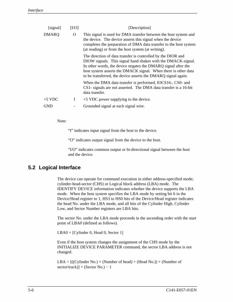
DMARQ O This signal is used for DMA transfer between the host system andthe device. The device asserts this signal when the devicecompletes the preparation of DMA data transfer to the host system(at reading) or from the host system (at writing).
The direction of data transfer is controlled by the DIOR andDIOW signals. This signal hand shakes with the DMACK-signal.In other words, the device negates the DMARQ signal after thehost system asserts the DMACK signal. When there is other datato be transferred, the device asserts the DMARQ signal again.
When the DMA data transfer is performed, IOCS16-, CS0- andCS1- signals are not asserted. The DMA data transfer is a 16-bitdata transfer.
+5 VDC I +5 VDC power supplying to the device.
GND - Grounded signal at each signal wire.
Note:
“I” indicates input signal from the host to the device.
“O” indicates output signal from the device to the host.
“I/O” indicates common output or bi-directional signal between the hostand the device.
5.2 Logical Interface
The device can operate for command execution in either address-specified mode;cylinder-head-sector (CHS) or Logical block address (LBA) mode. TheIDENTIFY DEVICE information indicates whether the device supports the LBAmode. When the host system specifies the LBA mode by setting bit 6 in theDevice/Head register to 1, HS3 to HS0 bits of the Device/Head register indicatesthe head No. under the LBA mode, and all bits of the Cylinder High, CylinderLow, and Sector Number registers are LBA bits.
The sector No. under the LBA mode proceeds in the ascending order with the startpoint of LBA0 (defined as follows).
LBA0 = [Cylinder 0, Head 0, Sector 1]
Even if the host system changes the assignment of the CHS mode by theINITIALIZE DEVICE PARAMETER command, the sector LBA address is notchanged.
LBA = [((Cylinder No.) × (Number of head) + (Head No.)) × (Number ofsector/track)] + (Sector No.) − 1
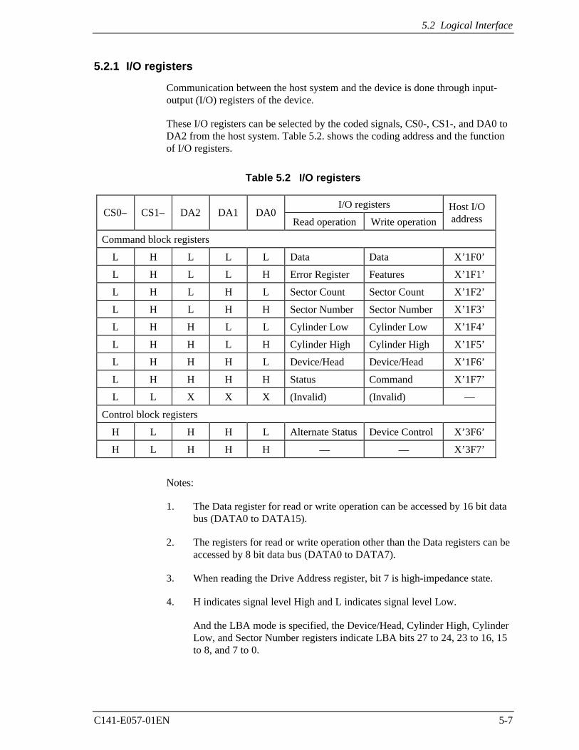
5.2 Logical Interface
C141-E057-01EN 5-7
5.2.1 I/O registers
Communication between the host system and the device is done through input-output (I/O) registers of the device.
These I/O registers can be selected by the coded signals, CS0-, CS1-, and DA0 toDA2 from the host system. Table 5.2. shows the coding address and the functionof I/O registers.
Table 5.2 I/O registers
I/O registers
Read operation Write operation
Command block registers
L H L L L Data Data X’1F0’
L H L L H Error Register Features X’1F1’
L H L H L Sector Count Sector Count X’1F2’
L H L H H Sector Number Sector Number X’1F3’
L H H L L Cylinder Low Cylinder Low X’1F4’
L H H L H Cylinder High Cylinder High X’1F5’
L H H H L Device/Head Device/Head X’1F6’
L H H H H Status Command X’1F7’
L L X X X (Invalid) (Invalid) —
Control block registers
H L H H L Alternate Status Device Control X’3F6’
H L H H H — — X’3F7’
Notes:
1. The Data register for read or write operation can be accessed by 16 bit databus (DATA0 to DATA15).
2. The registers for read or write operation other than the Data registers can beaccessed by 8 bit data bus (DATA0 to DATA7).
3. When reading the Drive Address register, bit 7 is high-impedance state.
4. H indicates signal level High and L indicates signal level Low.
And the LBA mode is specified, the Device/Head, Cylinder High, CylinderLow, and Sector Number registers indicate LBA bits 27 to 24, 23 to 16, 15to 8, and 7 to 0.
Host I/Oaddress
DA0DA1DA2CS1–CS0–
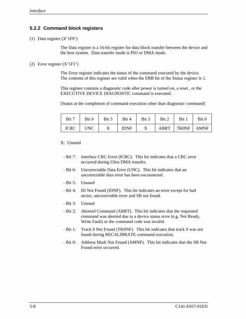
Interface
5-8 C141-E057-01EN
5.2.2 Command block registers
(1) Data register (X’1F0’)
The Data register is a 16-bit register for data block transfer between the device andthe host system. Data transfer mode is PIO or DMA mode.
(2) Error register (X’1F1’)
The Error register indicates the status of the command executed by the device.The contents of this register are valid when the ERR bit of the Status register is 1.
This register contains a diagnostic code after power is turned on, a reset , or theEXECUTIVE DEVICE DIAGNOSTIC command is executed.
[Status at the completion of command execution other than diagnostic command]
Bit 7 Bit 6 Bit 5 Bit 4 Bit 3 Bit 2 Bit 1 Bit 0
ICRC UNC X IDNF X ABRT TK0NF AMNF
X: Unused
- Bit 7: Interface CRC Error (ICRC). This bit indicates that a CRC erroroccurred during Ultra DMA transfer.
- Bit 6: Uncorrectable Data Error (UNC). This bit indicates that anuncorrectable data error has been encountered.
- Bit 5: Unused
- Bit 4: ID Not Found (IDNF). This bit indicates an error except for badsector, uncorrectable error and SB not found.
- Bit 3: Unused
- Bit 2: Aborted Command (ABRT). This bit indicates that the requestedcommand was aborted due to a device status error (e.g. Not Ready,Write Fault) or the command code was invalid.
- Bit 1: Track 0 Not Found (TK0NF). This bit indicates that track 0 was notfound during RECALIBRATE command execution.
- Bit 0: Address Mark Not Found (AMNF). This bit indicates that the SB NotFound error occurred.
5.2 Logical Interface
C141-E057-01EN 5-9
[Diagnostic code]
X’01’: No Error Detected.
X’02’: HDC Register Compare Error
X’03’: Data Buffer Compare Error.
X’05’: ROM Sum Check Error.
X’80’: Device 1 (slave device) Failed.
Error register of the master device is valid under two devices (masterand slave) configuration. If the slave device fails, the master deviceposts X’80’ OR (the diagnostic code) with its own status (X’01’ toX’05’).
However, when the host system selects the slave device, the diagnosticcode of the slave device is posted.
(3) Features register (X’1F1’)
The Features register provides specific feature to a command. For instance, it isused with SET FEATURES command to enable or disable caching.
(4) Sector Count register (X’1F2’)
The Sector Count register indicates the number of sectors of data to be transferredin a read or write operation between the host system and the device. When thevalue in this register is X’00’, the sector count is 256.
When this register indicates X’00’ at the completion of the command execution,this indicates that the command is completed succefully. If the command is notcompleted scuccessfully, this register indicates the number of sectors to betransferred to complete the request from the host system. That is, this registerindicates the number of remaining sectors that the data has not been transferreddue to the error.
The contents of this register has other definition for the following commands;INITIALIZE DEVICE PARAMETERS, SET FEATURES, IDLE, STANDBYand SET MULTIPLE MODE.
(5) Sector Number register (X’1F3’)
The contents of this register indicates the starting sector number for thesubsequent command. The sector number should be between X’01’ and [thenumber of sectors per track defined by INITIALIZE DEVICE PARAMETERScommand.
Under the LBA mode, this register indicates LBA bits 7 to 0.
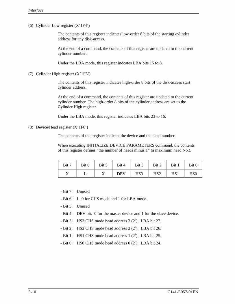
Interface
5-10 C141-E057-01EN
(6) Cylinder Low register (X’1F4’)
The contents of this register indicates low-order 8 bits of the starting cylinderaddress for any disk-access.
At the end of a command, the contents of this register are updated to the currentcylinder number.
Under the LBA mode, this register indcates LBA bits 15 to 8.
(7) Cylinder High register (X’1F5’)
The contents of this register indicates high-order 8 bits of the disk-access startcylinder address.
At the end of a command, the contents of this register are updated to the currentcylinder number. The high-order 8 bits of the cylinder address are set to theCylinder High register.
Under the LBA mode, this register indicates LBA bits 23 to 16.
(8) Device/Head register (X’1F6’)
The contents of this register indicate the device and the head number.
When executing INITIALIZE DEVICE PARAMETERS command, the contentsof this register defines “the number of heads minus 1” (a maximum head No.).
Bit 7 Bit 6 Bit 5 Bit 4 Bit 3 Bit 2 Bit 1 Bit 0
X L X DEV HS3 HS2 HS1 HS0
- Bit 7: Unused
- Bit 6: L. 0 for CHS mode and 1 for LBA mode.
- Bit 5: Unused
- Bit 4: DEV bit. 0 for the master device and 1 for the slave device.
- Bit 3: HS3 CHS mode head address 3 (23). LBA bit 27.
- Bit 2: HS2 CHS mode head address 2 (22). LBA bit 26.
- Bit 1: HS1 CHS mode head address 1 (21). LBA bit 25.
- Bit 0: HS0 CHS mode head address 0 (20). LBA bit 24.
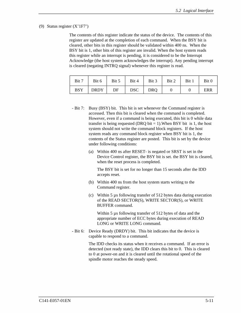
5.2 Logical Interface
C141-E057-01EN 5-11
(9) Status register (X’1F7’)
The contents of this register indicate the status of the device. The contents of thisregister are updated at the completion of each command. When the BSY bit iscleared, other bits in this register should be validated within 400 ns. When theBSY bit is 1, other bits of this register are invalid. When the host system readsthis register while an interrupt is pending, it is considered to be the InterruptAcknowledge (the host system acknowledges the interrupt). Any pending interruptis cleared (negating INTRQ signal) whenever this register is read.
Bit 7 Bit 6 Bit 5 Bit 4 Bit 3 Bit 2 Bit 1 Bit 0
BSY DRDY DF DSC DRQ 0 0 ERR
- Bit 7: Busy (BSY) bit. This bit is set whenever the Command register isaccessed. Then this bit is cleared when the command is completed.However, even if a command is being executed, this bit is 0 while datatransfer is being requested (DRQ bit = 1).When BSY bit is 1, the hostsystem should not write the command block registers. If the hostsystem reads any command block register when BSY bit is 1, thecontents of the Status register are posted. This bit is set by the deviceunder following conditions:
(a) Within 400 ns after RESET- is negated or SRST is set in theDevice Control register, the BSY bit is set. the BSY bit is cleared,when the reset process is completed.
The BSY bit is set for no longer than 15 seconds after the IDDaccepts reset.
(b) Within 400 ns from the host system starts writing to theCommand register.
(c) Within 5 µs following transfer of 512 bytes data during executionof the READ SECTOR(S), WRITE SECTOR(S), or WRITEBUFFER command.
Within 5 µs following transfer of 512 bytes of data and theappropriate number of ECC bytes during execution of READLONG or WRITE LONG command.
- Bit 6: Device Ready (DRDY) bit. This bit indicates that the device iscapable to respond to a command.
The IDD checks its status when it receives a command. If an error isdetected (not ready state), the IDD clears this bit to 0. This is clearedto 0 at power-on and it is cleared until the rotational speed of thespindle motor reaches the steady speed.
Interface
5-12 C141-E057-01EN
- Bit 5: The Device Write Fault (DF) bit. This bit indicates that a device fault(write fault) condition has been detected.
If a write fault is detected during command execution, this bit islatched and retained until the device accepts the next command orreset.
- Bit 4: Device Seek Complete (DSC) bit. This bit indicates that the deviceheads are positioned over a track.
In the IDD, this bit is always set to 1 after the spin-up control iscompleted.
- Bit 3: Data Request (DRQ) bit. This bit indicates that the device is ready totransfer data of word unit or byte unit between the host system and thedevice.
- Bit 2: Always 0.
- Bit 1: Always 0.
- Bit 0: Error (ERR) bit. This bit indicates that an error was detected while theprevious command was being executed. The Error register indicatesthe additional information of the cause for the error.
(10) Command register (X’1F7’)
The Command register contains a command code being sent to the device. Afterthis register is written, the command execution starts immediately.
Table 5.3 lists the executable commands and their command codes. This tablealso lists the neccesary parameters for each command which are written to certainregisters before the Command register is written.
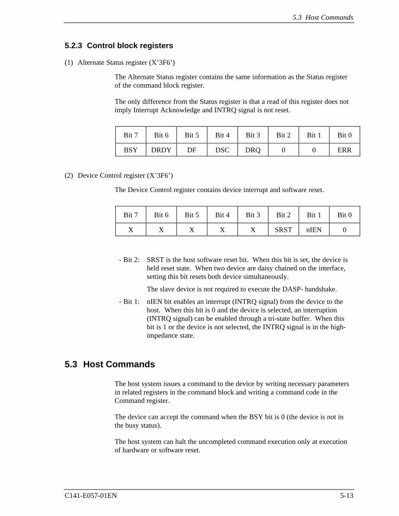
5.3 Host Commands
C141-E057-01EN 5-13
5.2.3 Control block registers
(1) Alternate Status register (X’3F6’)
The Alternate Status register contains the same information as the Status registerof the command block register.
The only difference from the Status register is that a read of this register does notimply Interrupt Acknowledge and INTRQ signal is not reset.
Bit 7 Bit 6 Bit 5 Bit 4 Bit 3 Bit 2 Bit 1 Bit 0
BSY DRDY DF DSC DRQ 0 0 ERR
(2) Device Control register (X’3F6’)
The Device Control register contains device interrupt and software reset.
Bit 7 Bit 6 Bit 5 Bit 4 Bit 3 Bit 2 Bit 1 Bit 0
X X X X X SRST nIEN 0
- Bit 2: SRST is the host software reset bit. When this bit is set, the device isheld reset state. When two device are daisy chained on the interface,setting this bit resets both device simultaneously.
The slave device is not required to execute the DASP- handshake.
- Bit 1: nIEN bit enables an interrupt (INTRQ signal) from the device to thehost. When this bit is 0 and the device is selected, an interruption(INTRQ signal) can be enabled through a tri-state buffer. When thisbit is 1 or the device is not selected, the INTRQ signal is in the high-impedance state.
5.3 Host Commands
The host system issues a command to the device by writing necessary parametersin related registers in the command block and writing a command code in theCommand register.
The device can accept the command when the BSY bit is 0 (the device is not inthe busy status).
The host system can halt the uncompleted command execution only at executionof hardware or software reset.
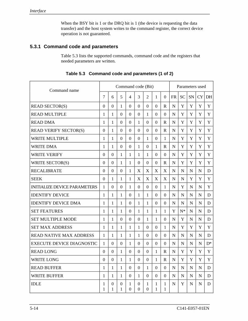
Interface
5-14 C141-E057-01EN
When the BSY bit is 1 or the DRQ bit is 1 (the device is requesting the datatransfer) and the host system writes to the command register, the correct deviceoperation is not guaranteed.
5.3.1 Command code and parameters
Table 5.3 lists the supported commands, command code and the registers thatneeded parameters are written.
Table 5.3 Command code and parameters (1 of 2)
Command code (Bit) Parameters used
7 6 5 4 3 2 1 0 FR SC SN CY DH
READ SECTOR(S) 0 0 1 0 0 0 0 R N Y Y Y Y
READ MULTIPLE 1 1 0 0 0 1 0 0 N Y Y Y Y
READ DMA 1 1 0 0 1 0 0 R N Y Y Y Y
READ VERIFY SECTOR(S) 0 1 0 0 0 0 0 R N Y Y Y Y
WRITE MULTIPLE 1 1 0 0 0 1 0 1 N Y Y Y Y
WRITE DMA 1 1 0 0 1 0 1 R N Y Y Y Y
WRITE VERIFY 0 0 1 1 1 1 0 0 N Y Y Y Y
WRITE SECTOR(S) 0 0 1 1 0 0 0 R N Y Y Y Y
RECALIBRATE 0 0 0 1 X X X X N N N N D
SEEK 0 1 1 1 X X X X N N Y Y Y
INITIALIZE DEVICE PARAMETERS 1 0 0 1 0 0 0 1 N Y N N Y
IDENTIFY DEVICE 1 1 1 0 1 1 0 0 N N N N D
IDENTIFY DEVICE DMA 1 1 1 0 1 1 0 0 N N N N D
SET FEATURES 1 1 1 0 1 1 1 1 Y N* N N D
SET MULTIPLE MODE 1 1 0 0 0 1 1 0 N Y N N D
SET MAX ADDRESS 1 1 1 1 1 0 0 1 N Y Y Y Y
READ NATIVE MAX ADDRESS 1 1 1 1 1 0 0 0 N N N N D
EXECUTE DEVICE DIAGNOSTIC 1 0 0 1 0 0 0 0 N N N N D*
READ LONG 0 0 1 0 0 0 1 R N Y Y Y Y
WRITE LONG 0 0 1 1 0 0 1 R N Y Y Y Y
READ BUFFER 1 1 1 0 0 1 0 0 N N N N D
WRITE BUFFER 1 1 1 0 1 0 0 0 N N N N D
IDLE 11
01
01
10
00
10
11
11
N Y N N D
Command name
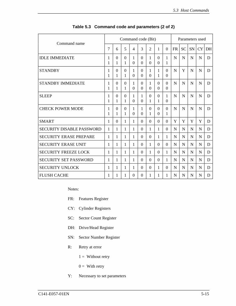
5.3 Host Commands
C141-E057-01EN 5-15
Table 5.3 Command code and parameters (2 of 2)
Command code (Bit) Parameters used
7 6 5 4 3 2 1 0 FR SC SN CY DH
IDLE IMMEDIATE 11
01
01
10
00
10
00
11
N N N N D
STANDBY 11
01
01
10
00
10
11
00
N Y N N D
STANDBY IMMEDIATE 11
01
01
10
00
10
00
00
N N N N D
SLEEP 11
01
01
10
10
01
01
10
N N N N D
CHECK POWER MODE 11
01
01
10
10
01
00
01
N N N N D
SMART 1 0 1 1 0 0 0 0 Y Y Y Y D
SECURITY DISABLE PASSWORD 1 1 1 1 0 1 1 0 N N N N D
SECURITY ERASE PREPARE 1 1 1 1 0 0 1 1 N N N N D
SECURITY ERASE UNIT 1 1 1 1 0 1 0 0 N N N N D
SECURITY FREEZE LOCK 1 1 1 1 0 1 0 1 N N N N D
SECURITY SET PASSWORD 1 1 1 1 0 0 0 1 N N N N D
SECURITY UNLOCK 1 1 1 1 0 0 1 0 N N N N D
FLUSH CACHE 1 1 1 0 0 1 1 1 N N N N D
Notes:
FR: Features Register
CY: Cylinder Registers
SC: Sector Count Register
DH: Drive/Head Register
SN: Sector Number Register
R: Retry at error
1 = Without retry
0 = With retry
Y: Necessary to set parameters
Command name
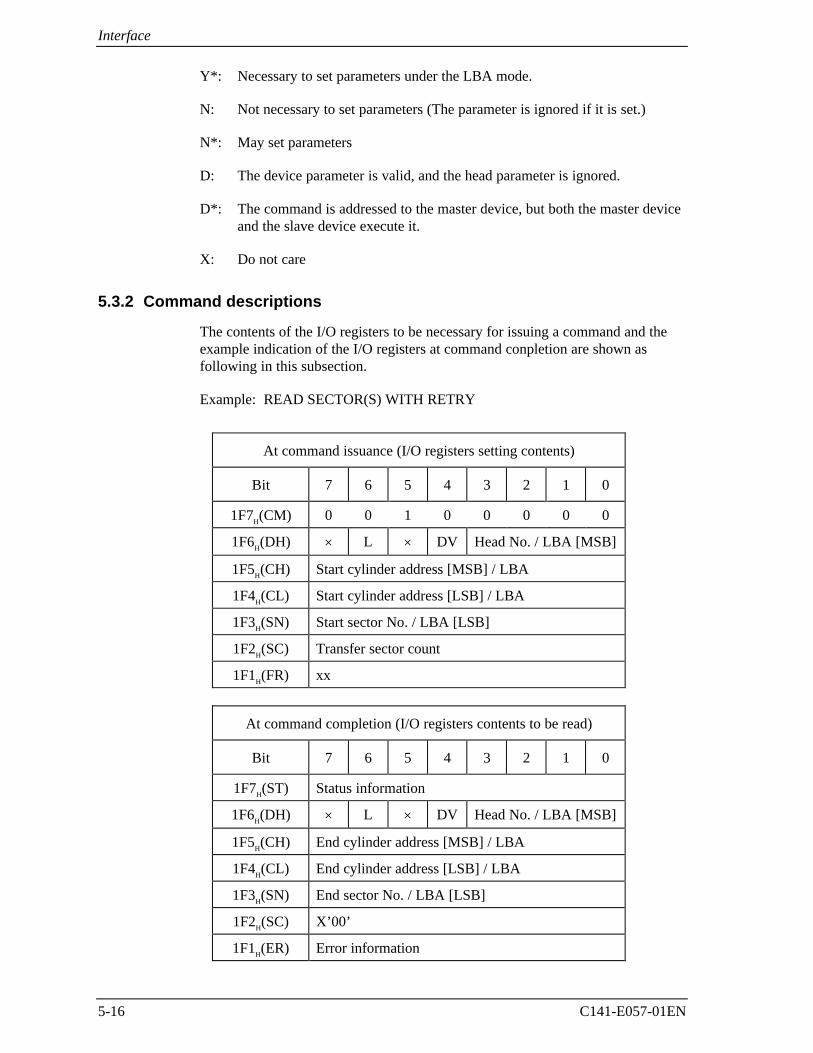
Interface
5-16 C141-E057-01EN
Y*: Necessary to set parameters under the LBA mode.
N: Not necessary to set parameters (The parameter is ignored if it is set.)
N*: May set parameters
D: The device parameter is valid, and the head parameter is ignored.
D*: The command is addressed to the master device, but both the master deviceand the slave device execute it.
X: Do not care
5.3.2 Command descriptions
The contents of the I/O registers to be necessary for issuing a command and theexample indication of the I/O registers at command conpletion are shown asfollowing in this subsection.
Example: READ SECTOR(S) WITH RETRY
At command issuance (I/O registers setting contents)
Bit 7 6 5 4 3 2 1 0
1F7H(CM) 0 0 1 0 0 0 0 0
1F6H(DH) × L × DV Head No. / LBA [MSB]
1F5H(CH) Start cylinder address [MSB] / LBA
1F4H(CL) Start cylinder address [LSB] / LBA
1F3H(SN) Start sector No. / LBA [LSB]
1F2H(SC) Transfer sector count
1F1H(FR) xx
At command completion (I/O registers contents to be read)
Bit 7 6 5 4 3 2 1 0
1F7H(ST) Status information
1F6H(DH) × L × DV Head No. / LBA [MSB]
1F5H(CH) End cylinder address [MSB] / LBA
1F4H(CL) End cylinder address [LSB] / LBA
1F3H(SN) End sector No. / LBA [LSB]
1F2H(SC) X’00’
1F1H(ER) Error information
5.3 Host Commands
C141-E057-01EN 5-17
CM: Command register FR: Features register
DH: Device/Head register ST: Status register
CH: Cylinder High register ER: Error register
CL: Cylinder Low register L: LBA (logical block address) setting bit
SN: Sector Number register DV: Device address. bit
SC: Sector Count register x, xx: Do not care (no necessary to set)
Note:
1. When the L bit is specified to 1, the lower 4 bits of the DH register and allbits of the CH, CL and SN registers indicate the LBA bits (bits of the DHregister are the MSB (most significant bit) and bits of the SN register arethe LSB (least significant bit).
2. At error occurrance, the SC register indicates the remaining sector count of datatransfer.
3. In the table indicating I/O registers contents in this subsection, bit indication isomitted.
(1) READ SECTOR(S) (X’20’ or X’21’)
This command reads data of sectors specified in the Sector Count register fromthe address specified in the Device/Head, Cylinder High, Cylinder Low andSector Number registers. Number of sectors can be specified to 256 sectors inmaximum. To specify 256 sectors reading, ‘00’ is specified. For the DRQ,INTRQ, and BSY protocols related to data transfer, see Subsection 5.4.1.
If the head is not on the track specified by the host, the device performs a impliedseek. After the head reaches to the specified track, the device reads the targetsector.
If an error occurs, retry reads are attempted to read the target sector beforereporting an error, irrespective of the R bit setting.
The DRQ bit of the Status register is always set prior to the data transferregardless of an error condition.
Upon the completion of the command execution, command block registers containthe cylinder, head, and sector addresses (in the CHS mode) or logical blockaddress (in the LBA mode) of the last sector read.
If an unrecoverable error occurs in a sector, the read operation is terminated at thesector where the error occured.
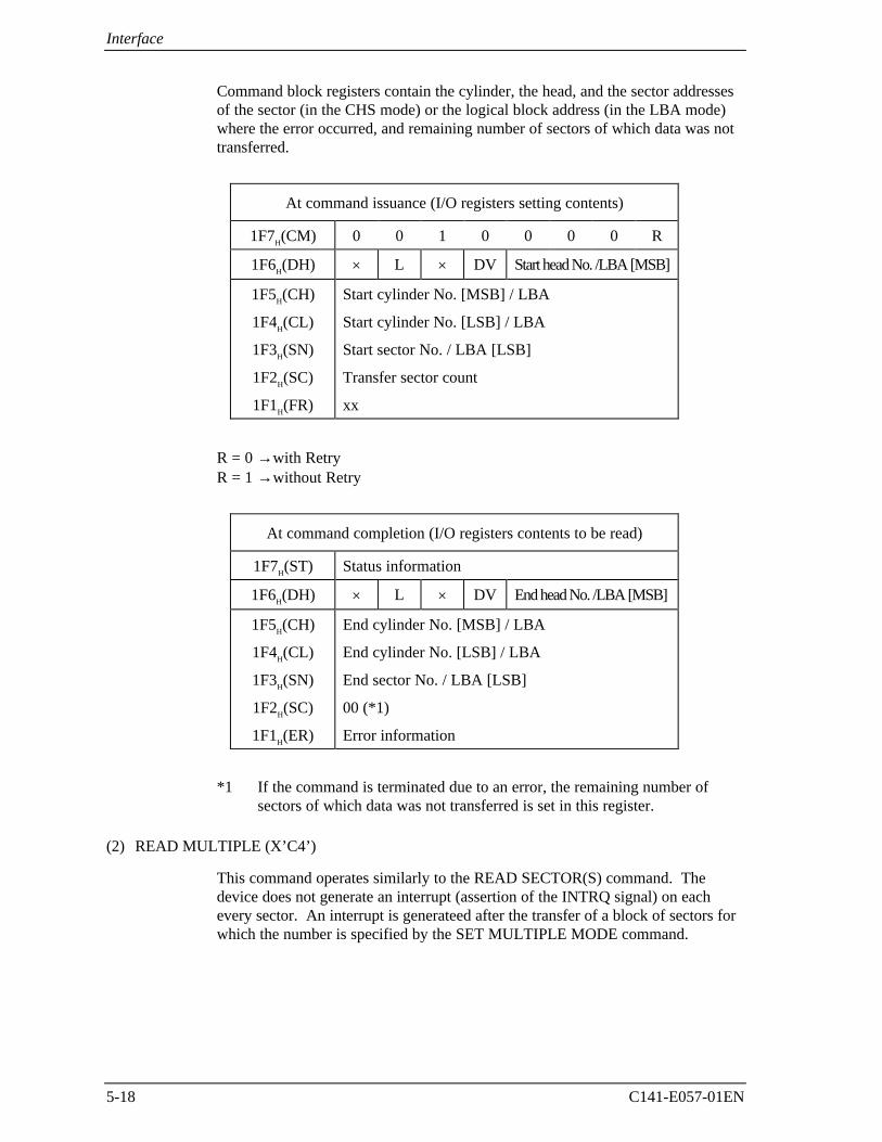
Interface
5-18 C141-E057-01EN
Command block registers contain the cylinder, the head, and the sector addressesof the sector (in the CHS mode) or the logical block address (in the LBA mode)where the error occurred, and remaining number of sectors of which data was nottransferred.
At command issuance (I/O registers setting contents)
1F7H(CM) 0 0 1 0 0 0 0 R
1F6H(DH) × L × DV Start head No. /LBA [MSB]
1F5H(CH)
1F4H(CL)
1F3H(SN)
1F2H(SC)
1F1H(FR)
Start cylinder No. [MSB] / LBA
Start cylinder No. [LSB] / LBA
Start sector No. / LBA [LSB]
Transfer sector count
xx
R = 0 →with RetryR = 1 →without Retry
At command completion (I/O registers contents to be read)
1F7H(ST) Status information
1F6H(DH) × L × DV End head No. /LBA [MSB]
1F5H(CH)
1F4H(CL)
1F3H(SN)
1F2H(SC)
1F1H(ER)
End cylinder No. [MSB] / LBA
End cylinder No. [LSB] / LBA
End sector No. / LBA [LSB]
00 (*1)
Error information
*1 If the command is terminated due to an error, the remaining number ofsectors of which data was not transferred is set in this register.
(2) READ MULTIPLE (X’C4’)
This command operates similarly to the READ SECTOR(S) command. Thedevice does not generate an interrupt (assertion of the INTRQ signal) on eachevery sector. An interrupt is generateed after the transfer of a block of sectors forwhich the number is specified by the SET MULTIPLE MODE command.
5.3 Host Commands
C141-E057-01EN 5-19
The implementation of the READ MULTIPLE command is identical to that of theREAD SECTOR(S) command except that the number of sectors is specified bythe SET MULTIPLE MODE command are transferred without interveninginterrupts. In the READ MULTIPLE command operation, the DRQ bit of theStatus register is set only at the start of the data block, and is not set on eachsector.
The number of sectors (block count) to be transferred without interruption isspecifed by the SET MULTIPLE MODE command. The SET MULTIPLEMODE command should be executed prior to the READ MULTIPLE command.
When the READ MULTIPLE command is issued, the Sector Count registercontains the number of sectors requested (not a number of the block count or anumber of sectors in a block).
Upon receipt of this command, the device executes this command even if thevalue of the Sector Count register is less than the defined block count (the valueof the Sector Count should not be 0).
If the number of requested sectors is not divided evenly (having the same numberof sectors [block count]), as many full blocks as possible are transferred, then afinal partial block is transferred. The number of sectors in the partial block to betransferred is n where n = remainder of (“number of sectors”/”block count”).
If the READ MULTIPLE command is issued before the SET MULTIPLE MODEcommand is executed or when the READ MULTIPLE command is disabled, thedevice rejects the READ MULTIPLE command with an ABORTED COMMANDerror.
If an unrecoverable error occurs, reading sector is stopped at the sector where theerror occurred. Command block registers contain the cylinder, the head, thesector addresses (in the CHS mode) or the logical block address (in the LBAmode) of the sector where the error occurred, and remaining number of sectorsthat had not transferred after the sector where the error occurred.
An interrupt is generated when the DRQ bit is set at the beginning of each block or apartial block.
Figure 5.2 shows an example of the execution of the READ MULTIPLEcommand.
• Block count specified by SET MULTIPLE MODE command = 4 (number ofsectors in a block)
• READ MULTIPLE command specifies;
Number of requested sectors = 9 (Sector Count register = 9)
↓
Number of sectors in incomplete block = remainder of 9/4 =1
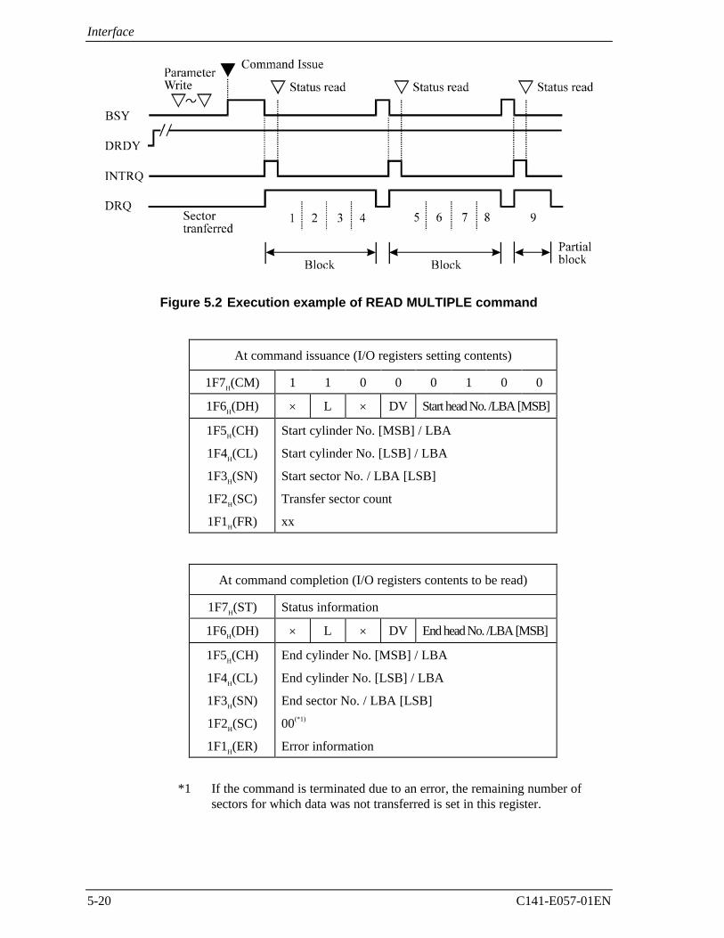
Interface
5-20 C141-E057-01EN
Figure 5.2 Execution example of READ MULTIPLE command
At command issuance (I/O registers setting contents)
1F7H(CM) 1 1 0 0 0 1 0 0
1F6H(DH) × L × DV Start head No. /LBA [MSB]
1F5H(CH)
1F4H(CL)
1F3H(SN)
1F2H(SC)
1F1H(FR)
Start cylinder No. [MSB] / LBA
Start cylinder No. [LSB] / LBA
Start sector No. / LBA [LSB]
Transfer sector count
xx
At command completion (I/O registers contents to be read)
1F7H(ST) Status information
1F6H(DH) × L × DV End head No. /LBA [MSB]
1F5H(CH)
1F4H(CL)
1F3H(SN)
1F2H(SC)
1F1H(ER)
End cylinder No. [MSB] / LBA
End cylinder No. [LSB] / LBA
End sector No. / LBA [LSB]
00(*1)
Error information
*1 If the command is terminated due to an error, the remaining number ofsectors for which data was not transferred is set in this register.
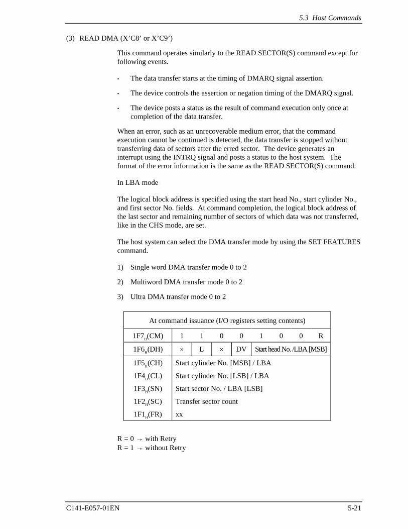
5.3 Host Commands
C141-E057-01EN 5-21
(3) READ DMA (X’C8’ or X’C9’)
This command operates similarly to the READ SECTOR(S) command except forfollowing events.
• The data transfer starts at the timing of DMARQ signal assertion.
• The device controls the assertion or negation timing of the DMARQ signal.
• The device posts a status as the result of command execution only once atcompletion of the data transfer.
When an error, such as an unrecoverable medium error, that the commandexecution cannot be continued is detected, the data transfer is stopped withouttransferring data of sectors after the erred sector. The device generates aninterrupt using the INTRQ signal and posts a status to the host system. Theformat of the error information is the same as the READ SECTOR(S) command.
In LBA mode
The logical block address is specified using the start head No., start cylinder No.,and first sector No. fields. At command completion, the logical block address ofthe last sector and remaining number of sectors of which data was not transferred,like in the CHS mode, are set.
The host system can select the DMA transfer mode by using the SET FEATUREScommand.
1) Single word DMA transfer mode 0 to 2
2) Multiword DMA transfer mode 0 to 2
3) Ultra DMA transfer mode 0 to 2
At command issuance (I/O registers setting contents)
1F7H(CM) 1 1 0 0 1 0 0 R
1F6H(DH) × L × DV Start head No. /LBA [MSB]
1F5H(CH)
1F4H(CL)
1F3H(SN)
1F2H(SC)
1F1H(FR)
Start cylinder No. [MSB] / LBA
Start cylinder No. [LSB] / LBA
Start sector No. / LBA [LSB]
Transfer sector count
xx
R = 0 → with RetryR = 1 → without Retry
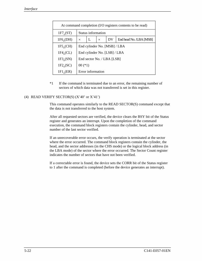
Interface
5-22 C141-E057-01EN
At command completion (I/O registers contents to be read)
1F7H(ST) Status information
1F6H(DH) × L × DV End head No. /LBA [MSB]
1F5H(CH)
1F4H(CL)
1F3H(SN)
1F2H(SC)
1F1H(ER)
End cylinder No. [MSB] / LBA
End cylinder No. [LSB] / LBA
End sector No. / LBA [LSB]
00 (*1)
Error information
*1 If the command is terminated due to an error, the remaining number ofsectors of which data was not transferred is set in this register.
(4) READ VERIFY SECTOR(S) (X’40’ or X’41’)
This command operates similarly to the READ SECTOR(S) command except thatthe data is not transferred to the host system.
After all requested sectors are verified, the device clears the BSY bit of the Statusregister and generates an interrupt. Upon the completion of the commandexecution, the command block registers contain the cylinder, head, and sectornumber of the last sector verified.
If an unrecoverable error occurs, the verify operation is terminated at the sectorwhere the error occurred. The command block registers contain the cylinder, thehead, and the sector addresses (in the CHS mode) or the logical block address (inthe LBA mode) of the sector where the error occurred. The Sector Count registerindicates the number of sectors that have not been verified.
If a correctable error is found, the device sets the CORR bit of the Status registerto 1 after the command is completed (before the device generates an interrupt).
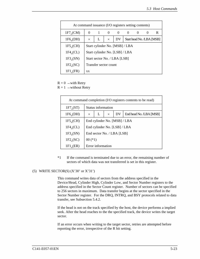
5.3 Host Commands
C141-E057-01EN 5-23
At command issuance (I/O registers setting contents)
1F7H(CM) 0 1 0 0 0 0 0 R
1F6H(DH) × L × DV Start head No. /LBA [MSB]
1F5H(CH)
1F4H(CL)
1F3H(SN)
1F2H(SC)
1F1H(FR)
Start cylinder No. [MSB] / LBA
Start cylinder No. [LSB] / LBA
Start sector No. / LBA [LSB]
Transfer sector count
xx
R = 0 →with RetryR = 1 →without Retry
At command completion (I/O registers contents to be read)
1F7H(ST) Status information
1F6H(DH) × L × DV End head No. /LBA [MSB]
1F5H(CH)
1F4H(CL)
1F3H(SN)
1F2H(SC)
1F1H(ER)
End cylinder No. [MSB] / LBA
End cylinder No. [LSB] / LBA
End sector No. / LBA [LSB]
00 (*1)
Error information
*1 If the command is terminated due to an error, the remaining number ofsectors of which data was not transferred is set in this register.
(5) WRITE SECTOR(S) (X’30’ or X’31’)
This command writes data of sectors from the address specified in theDevice/Head, Cylinder High, Cylinder Low, and Sector Number registers to theaddress specified in the Sector Count register. Number of sectors can be specifiedto 256 sectors in maximum. Data transfer begins at the sector specified in theSector Number register. For the DRQ, INTRQ, and BSY protocols related to datatransfer, see Subsection 5.4.2.
If the head is not on the track specified by the host, the device performs a impliedseek. After the head reaches to the the specified track, the device writes the targetsector.
If an error occurs when writing to the target sector, retries are attempted beforereporting the error, irrespective of the R bit setting.
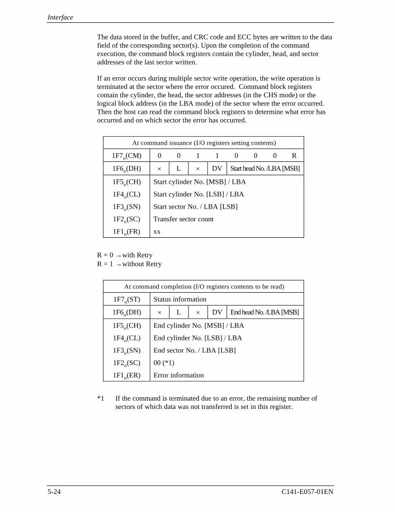
Interface
5-24 C141-E057-01EN
The data stored in the buffer, and CRC code and ECC bytes are written to the datafield of the corresponding sector(s). Upon the completion of the commandexecution, the command block registers contain the cylinder, head, and sectoraddresses of the last sector written.
If an error occurs during multiple sector write operation, the write operation isterminated at the sector where the error occured. Command block registerscontain the cylinder, the head, the sector addresses (in the CHS mode) or thelogical block address (in the LBA mode) of the sector where the error occurred.Then the host can read the command block registers to determine what error hasoccurred and on which sector the error has occurred.
At command issuance (I/O registers setting contents)
1F7H(CM) 0 0 1 1 0 0 0 R
1F6H(DH) × L × DV Start head No. /LBA [MSB]
1F5H(CH)
1F4H(CL)
1F3H(SN)
1F2H(SC)
1F1H(FR)
Start cylinder No. [MSB] / LBA
Start cylinder No. [LSB] / LBA
Start sector No. / LBA [LSB]
Transfer sector count
xx
R = 0 →with RetryR = 1 →without Retry
At command completion (I/O registers contents to be read)
1F7H(ST) Status information
1F6H(DH) × L × DV End head No. /LBA [MSB]
1F5H(CH)
1F4H(CL)
1F3H(SN)
1F2H(SC)
1F1H(ER)
End cylinder No. [MSB] / LBA
End cylinder No. [LSB] / LBA
End sector No. / LBA [LSB]
00 (*1)
Error information
*1 If the command is terminated due to an error, the remaining number ofsectors of which data was not transferred is set in this register.
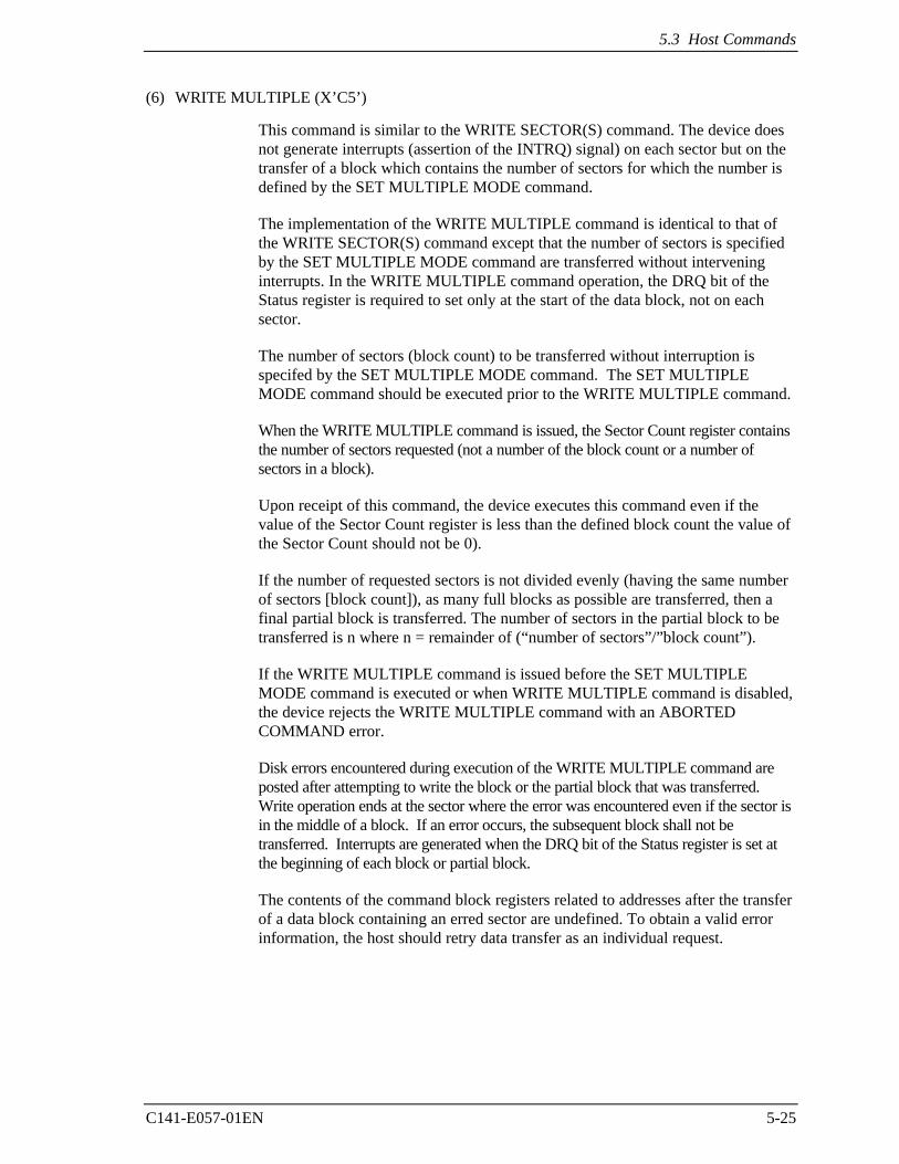
5.3 Host Commands
C141-E057-01EN 5-25
(6) WRITE MULTIPLE (X’C5’)
This command is similar to the WRITE SECTOR(S) command. The device doesnot generate interrupts (assertion of the INTRQ) signal) on each sector but on thetransfer of a block which contains the number of sectors for which the number isdefined by the SET MULTIPLE MODE command.
The implementation of the WRITE MULTIPLE command is identical to that ofthe WRITE SECTOR(S) command except that the number of sectors is specifiedby the SET MULTIPLE MODE command are transferred without interveninginterrupts. In the WRITE MULTIPLE command operation, the DRQ bit of theStatus register is required to set only at the start of the data block, not on eachsector.
The number of sectors (block count) to be transferred without interruption isspecifed by the SET MULTIPLE MODE command. The SET MULTIPLEMODE command should be executed prior to the WRITE MULTIPLE command.
When the WRITE MULTIPLE command is issued, the Sector Count register containsthe number of sectors requested (not a number of the block count or a number ofsectors in a block).
Upon receipt of this command, the device executes this command even if thevalue of the Sector Count register is less than the defined block count the value ofthe Sector Count should not be 0).
If the number of requested sectors is not divided evenly (having the same numberof sectors [block count]), as many full blocks as possible are transferred, then afinal partial block is transferred. The number of sectors in the partial block to betransferred is n where n = remainder of (“number of sectors”/”block count”).
If the WRITE MULTIPLE command is issued before the SET MULTIPLEMODE command is executed or when WRITE MULTIPLE command is disabled,the device rejects the WRITE MULTIPLE command with an ABORTEDCOMMAND error.
Disk errors encountered during execution of the WRITE MULTIPLE command areposted after attempting to write the block or the partial block that was transferred.Write operation ends at the sector where the error was encountered even if the sector isin the middle of a block. If an error occurs, the subsequent block shall not betransferred. Interrupts are generated when the DRQ bit of the Status register is set atthe beginning of each block or partial block.
The contents of the command block registers related to addresses after the transferof a data block containing an erred sector are undefined. To obtain a valid errorinformation, the host should retry data transfer as an individual request.
Interface
5-26 C141-E057-01EN
At command issuance (I/O registers setting contents)
1F7H(CM) 1 1 0 0 0 1 0 1
1F6H(DH) × L × DV Start head No. /LBA [MSB]
1F5H(CH)
1F4H(CL)
1F3H(SN)
1F2H(SC)
1F1H(FR)
Start cylinder No. [MSB] / LBA
Start cylinder No. [LSB] / LBA
Start sector No. / LBA [LSB]
Transfer sector count
xx
At command completion (I/O registers contents to be read)
1F7H(ST) Status information
1F6H(DH) × L × DV End head No. /LBA [MSB]
1F5H(CH)
1F4H(CL)
1F3H(SN)
1F2H(SC)
1F1H(ER)
End cylinder No. [MSB] / LBA
End cylinder No. [LSB] / LBA
End sector No. / LBA [LSB]
00
Error information
(7) WRITE DMA (X’CA’ or X’CB’)
This command operates similarly to the WRITE SECTOR(S) command except forfollowing events.
• The data transfer starts at the timing of DMARQ signal assertion.
• The device controls the assertion or negation timing of the DMARQ signal.
• The device posts a status as the result of command execution only once atcompletion of the data transfer or completion of processing in the device.
• The device posts a status as the result of command execution only once atcompletion of the data transfer.
When an error, such as an unrecoverable medium error, that the commandexecution cannot be continued is detected, the data transfer is stopped withouttransferring data of sectors after the erred sector. The device generates aninterrupt using the INTRQ signal and posts a status to the host system. Theformat of the error information is the same as the WRITE SECTOR(S) command.
5.3 Host Commands
C141-E057-01EN 5-27
A host system can select the following transfer mode using the SET FEATUREScommand.
1) Single word DMA transfer mode 0 to 2
2) Multiword DMA transfer mode 0 to 2
3) Ultra DMA transfer mode 0 to 2
At command issuance (I/O registers setting contents)
1F7H(CM) 1 1 0 0 1 0 1 R
1F6H(DH) × L × DV Start head No. /LBA [MSB]
1F5H(CH)
1F4H(CL)
1F3H(SN)
1F2H(SC)
1F1H(FR)
Start cylinder No. [MSB] / LBA
Start cylinder No. [LSB] / LBA
Start sector No. / LBA [LSB]
Transfer sector count
xx
R = 0 →with RetryR = 1 →without Retry
At command completion (I/O registers contents to be read)
1F7H(ST) Status information
1F6H(DH) × L × DV End head No. /LBA [MSB]
1F5H(CH)
1F4H(CL)
1F3H(SN)
1F2H(SC)
1F1H(ER)
End cylinder No. [MSB] / LBA
End cylinder No. [LSB] / LBA
End sector No. / LBA [LSB]
00 (*1)
Error information
*1 If the command is terminated due to an error, the remaining number ofsectors of which data was not transferred is set in this register.
(8) WRITE VERIFY (X’3C’)
This command operates similarly to the WRITE SECTOR(S) command exceptthat the device verifies each sector immediately after being written. The verifyoperation is a read and check for data errors without data transfer. Any error thatis detected during the verify operation is posted.
Interface
5-28 C141-E057-01EN
After all sectors are verified, the last interruption (INTRQ for commandtermination) is generated.
At command issuance (I/O registers setting contents)
1F7H(CM) 0 0 1 1 1 1 0 0
1F6H(DH) × L × DV Start head No. /LBA [MSB]
1F5H(CH)
1F4H(CL)
1F3H(SN)
1F2H(SC)
1F1H(FR)
Start cylinder No. [MSB] / LBA
Start cylinder No. [LSB] / LBA
Start sector No. / LBA [LSB]
Transfer sector count
xx
At command completion (I/O registers contents to be read)
1F7H(ST) Status information
1F6H(DH) × L × DV End head No. /LBA [MSB]
1F5H(CH)
1F4H(CL)
1F3H(SN)
1F2H(SC)
1F1H(ER)
End cylinder No. [MSB] / LBA
End cylinder No. [LSB] / LBA
End sector No. / LBA [LSB]
00 (*1)
Error information
*1 If the command is terminated due to an error, the remaining number ofsectors of which data was not transferred is set in this register.
(9) RECALIBRATE (X’1x’, x: X’0’ to X’F’)
This command performs the calibration. Upon receipt of this command, thedevice sets BSY bit of the Status register and performs a calibration. When thedevice completes the calibration, the device updates the Status register, clears theBSY bit, and generates an interrupt.
This command can be issued in the LBA mode.
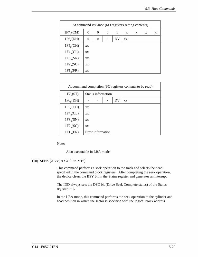
5.3 Host Commands
C141-E057-01EN 5-29
At command issuance (I/O registers setting contents)
1F7H(CM) 0 0 0 1 x x x x
1F6H(DH) × × × DV xx
1F5H(CH)
1F4H(CL)
1F3H(SN)
1F2H(SC)
1F1H(FR)
xx
xx
xx
xx
xx
At command completion (I/O registers contents to be read)
1F7H(ST) Status information
1F6H(DH) × × × DV xx
1F5H(CH)
1F4H(CL)
1F3H(SN)
1F2H(SC)
1F1H(ER)
xx
xx
xx
xx
Error information
Note:
Also executable in LBA mode.
(10) SEEK (X’7x’, x : X’0’ to X’F’)
This command performs a seek operation to the track and selects the headspecified in the command block registers. After completing the seek operation,the device clears the BSY bit in the Status register and generates an interrupt.
The IDD always sets the DSC bit (Drive Seek Complete status) of the Statusregister to 1.
In the LBA mode, this command performs the seek operation to the cylinder andhead position in which the sector is specified with the logical block address.
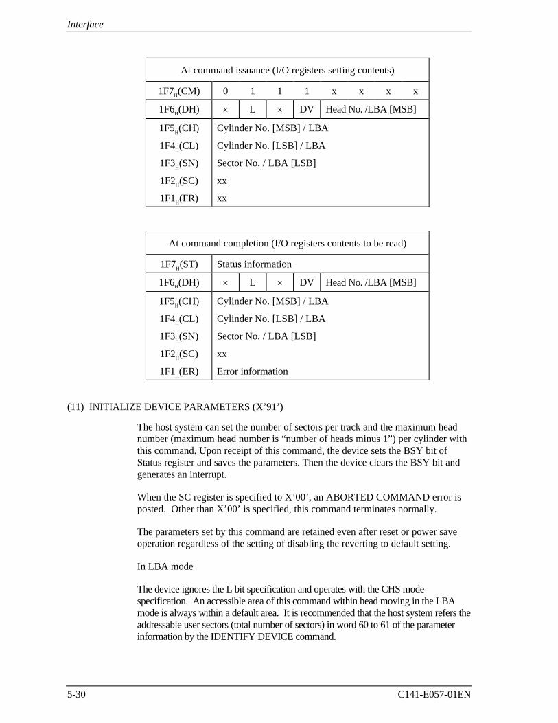
Interface
5-30 C141-E057-01EN
At command issuance (I/O registers setting contents)
1F7H(CM) 0 1 1 1 x x x x
1F6H(DH) × L × DV Head No. /LBA [MSB]
1F5H(CH)
1F4H(CL)
1F3H(SN)
1F2H(SC)
1F1H(FR)
Cylinder No. [MSB] / LBA
Cylinder No. [LSB] / LBA
Sector No. / LBA [LSB]
xx
xx
At command completion (I/O registers contents to be read)
1F7H(ST) Status information
1F6H(DH) × L × DV Head No. /LBA [MSB]
1F5H(CH)
1F4H(CL)
1F3H(SN)
1F2H(SC)
1F1H(ER)
Cylinder No. [MSB] / LBA
Cylinder No. [LSB] / LBA
Sector No. / LBA [LSB]
xx
Error information
(11) INITIALIZE DEVICE PARAMETERS (X’91’)
The host system can set the number of sectors per track and the maximum headnumber (maximum head number is “number of heads minus 1”) per cylinder withthis command. Upon receipt of this command, the device sets the BSY bit ofStatus register and saves the parameters. Then the device clears the BSY bit andgenerates an interrupt.
When the SC register is specified to X’00’, an ABORTED COMMAND error isposted. Other than X’00’ is specified, this command terminates normally.
The parameters set by this command are retained even after reset or power saveoperation regardless of the setting of disabling the reverting to default setting.
In LBA mode
The device ignores the L bit specification and operates with the CHS modespecification. An accessible area of this command within head moving in the LBAmode is always within a default area. It is recommended that the host system refers theaddressable user sectors (total number of sectors) in word 60 to 61 of the parameterinformation by the IDENTIFY DEVICE command.
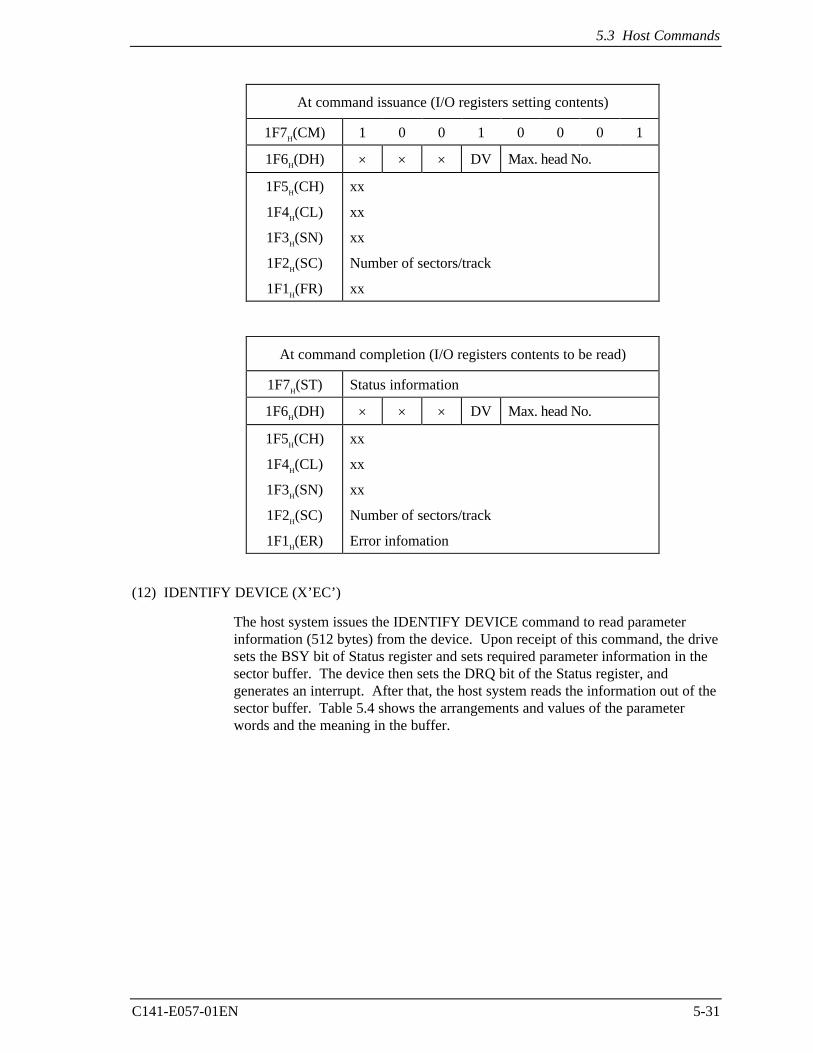
5.3 Host Commands
C141-E057-01EN 5-31
At command issuance (I/O registers setting contents)
1F7H(CM) 1 0 0 1 0 0 0 1
1F6H(DH) × × × DV Max. head No.
1F5H(CH)
1F4H(CL)
1F3H(SN)
1F2H(SC)
1F1H(FR)
xx
xx
xx
Number of sectors/track
xx
At command completion (I/O registers contents to be read)
1F7H(ST) Status information
1F6H(DH) × × × DV Max. head No.
1F5H(CH)
1F4H(CL)
1F3H(SN)
1F2H(SC)
1F1H(ER)
xx
xx
xx
Number of sectors/track
Error infomation
(12) IDENTIFY DEVICE (X’EC’)
The host system issues the IDENTIFY DEVICE command to read parameterinformation (512 bytes) from the device. Upon receipt of this command, the drivesets the BSY bit of Status register and sets required parameter information in thesector buffer. The device then sets the DRQ bit of the Status register, andgenerates an interrupt. After that, the host system reads the information out of thesector buffer. Table 5.4 shows the arrangements and values of the parameterwords and the meaning in the buffer.
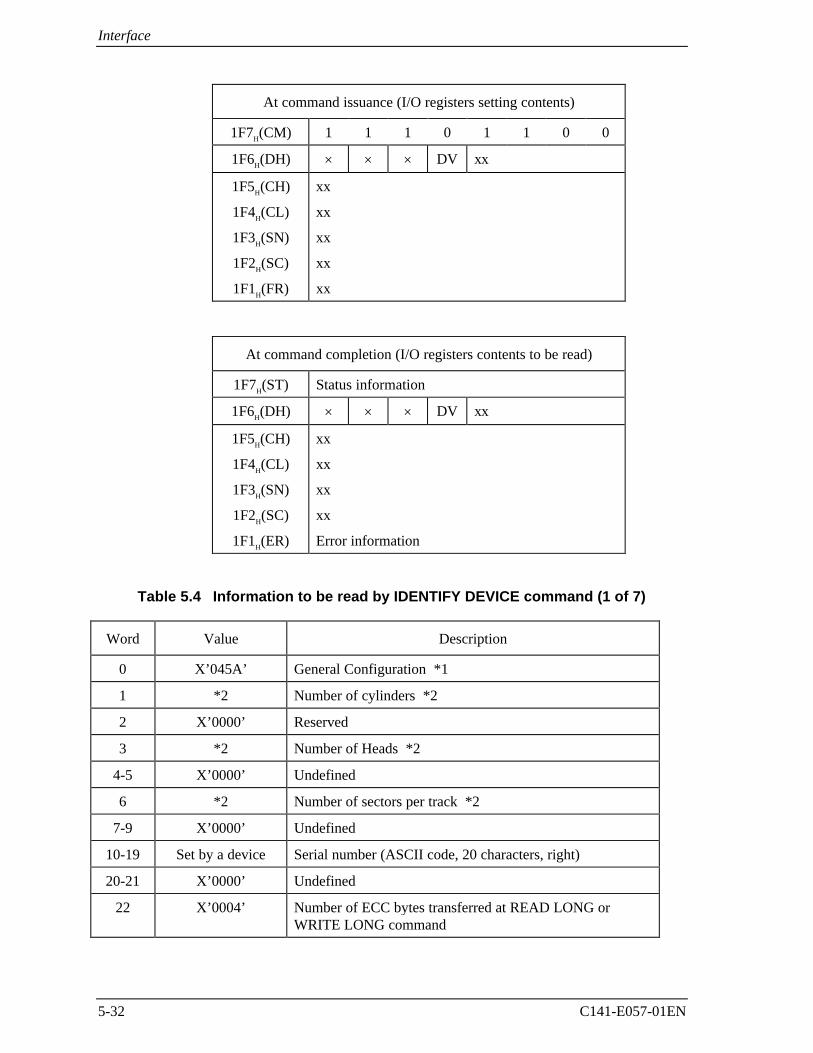
Interface
5-32 C141-E057-01EN
At command issuance (I/O registers setting contents)
1F7H(CM) 1 1 1 0 1 1 0 0
1F6H(DH) × × × DV xx
1F5H(CH)
1F4H(CL)
1F3H(SN)
1F2H(SC)
1F1H(FR)
xx
xx
xx
xx
xx
At command completion (I/O registers contents to be read)
1F7H(ST) Status information
1F6H(DH) × × × DV xx
1F5H(CH)
1F4H(CL)
1F3H(SN)
1F2H(SC)
1F1H(ER)
xx
xx
xx
xx
Error information
Table 5.4 Information to be read by IDENTIFY DEVICE command (1 of 7)
Word Value Description
0 X’045A’ General Configuration *1
1 *2 Number of cylinders *2
2 X’0000’ Reserved
3 *2 Number of Heads *2
4-5 X’0000’ Undefined
6 *2 Number of sectors per track *2
7-9 X’0000’ Undefined
10-19 Set by a device Serial number (ASCII code, 20 characters, right)
20-21 X’0000’ Undefined
22 X’0004’ Number of ECC bytes transferred at READ LONG orWRITE LONG command
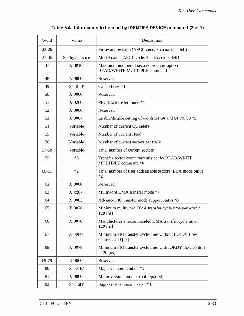
5.3 Host Commands
C141-E057-01EN 5-33
Table 5.4 Information to be read by IDENTIFY DEVICE command (2 of 7)
Word Value Description
23-26 – Firmware revision (ASCII code, 8 characters, left)
27-46 Set by a device Model name (ASCII code, 40 characters, left)
47 X’8010’ Maximum number of sectors per interrupt onREAD/WRITE MULTIPLE command
48 X’0000’ Reserved
49 X’0B00’ Capabilities *3
50 X’0000’ Reserved
51 X’0200’ PIO data transfer mode *4
52 X’0000’ Reserved
53 X’0007’ Enable/disable setting of words 54-58 and 64-70, 88 *5
54 (Variable) Number of current Cylinders
55 (Variable) Number of current Head
56 (Variable) Number of current sectors per track
57-58 (Variable) Total number of current sectors
59 *6 Transfer sector count currently set by READ/WRITEMULTIPLE command *6
60-61 *2 Total number of user addressable sectors (LBA mode only)*2
62 X’0000’ Reserved
63 X’xx07’ Multiword DMA transfer mode *7
64 X’0003’ Advance PIO transfer mode support status *8
65 X’0078’ Minimum multiword DMA transfer cycle time per word :120 [ns]
66 X’0078’ Manufacturer’s recommended DMA transfer cycle time :120 [ns]
67 X’00F0’ Minimum PIO transfer cycle time without IORDY flowcontrol : 240 [ns]
68 X’0078’ Minimum PIO transfer cycle time with IORDY flow control: 120 [ns]
69-79 X’0000’ Reserved
80 X’001E’ Major version number *9
81 X’0000’ Minor version number (not reported)
82 X’346B’ Support of command sets *10
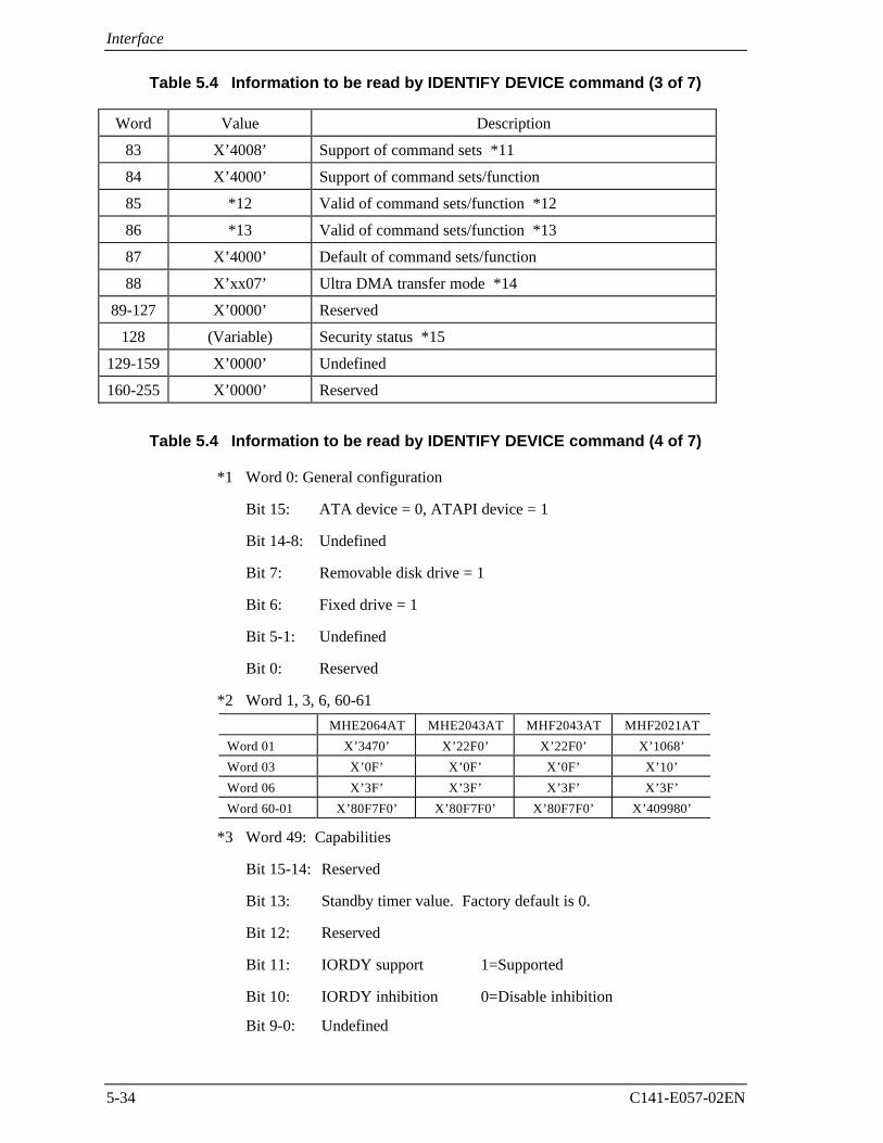
Interface
5-34 C141-E057-02EN
Table 5.4 Information to be read by IDENTIFY DEVICE command (3 of 7)
Word Value Description
83 X’4008’ Support of command sets *11
84 X’4000’ Support of command sets/function
85 *12 Valid of command sets/function *12
86 *13 Valid of command sets/function *13
87 X’4000’ Default of command sets/function
88 X’xx07’ Ultra DMA transfer mode *14
89-127 X’0000’ Reserved
128 (Variable) Security status *15
129-159 X’0000’ Undefined
160-255 X’0000’ Reserved
Table 5.4 Information to be read by IDENTIFY DEVICE command (4 of 7)
*1 Word 0: General configuration
Bit 15: ATA device = 0, ATAPI device = 1
Bit 14-8: Undefined
Bit 7: Removable disk drive = 1
Bit 6: Fixed drive = 1
Bit 5-1: Undefined
Bit 0: Reserved
*2 Word 1, 3, 6, 60-61
MHE2064AT MHE2043AT MHF2043AT MHF2021AT
Word 01 X’3470’ X’22F0’ X’22F0’ X’1068’
Word 03 X’0F’ X’0F’ X’0F’ X’10’
Word 06 X’3F’ X’3F’ X’3F’ X’3F’
Word 60-01 X’80F7F0’ X’80F7F0’ X’80F7F0’ X’409980’
*3 Word 49: Capabilities
Bit 15-14: Reserved
Bit 13: Standby timer value. Factory default is 0.
Bit 12: Reserved
Bit 11: IORDY support 1=Supported
Bit 10: IORDY inhibition 0=Disable inhibition
Bit 9-0: Undefined
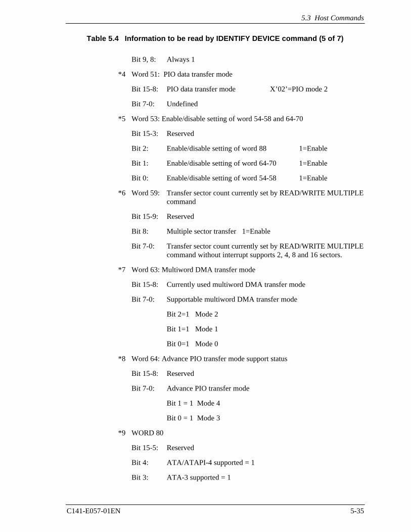
5.3 Host Commands
C141-E057-01EN 5-35
Table 5.4 Information to be read by IDENTIFY DEVICE command (5 of 7)
Bit 9, 8: Always 1
*4 Word 51: PIO data transfer mode
Bit 15-8: PIO data transfer mode X’02’=PIO mode 2
Bit 7-0: Undefined
*5 Word 53: Enable/disable setting of word 54-58 and 64-70
Bit 15-3: Reserved
Bit 2: Enable/disable setting of word 88 1=Enable
Bit 1: Enable/disable setting of word 64-70 1=Enable
Bit 0: Enable/disable setting of word 54-58 1=Enable
*6 Word 59: Transfer sector count currently set by READ/WRITE MULTIPLEcommand
Bit 15-9: Reserved
Bit 8: Multiple sector transfer 1=Enable
Bit 7-0: Transfer sector count currently set by READ/WRITE MULTIPLEcommand without interrupt supports 2, 4, 8 and 16 sectors.
*7 Word 63: Multiword DMA transfer mode
Bit 15-8: Currently used multiword DMA transfer mode
Bit 7-0: Supportable multiword DMA transfer mode
Bit 2=1 Mode 2
Bit 1=1 Mode 1
Bit 0=1 Mode 0
*8 Word 64: Advance PIO transfer mode support status
Bit 15-8: Reserved
Bit 7-0: Advance PIO transfer mode
Bit 1 = 1 Mode 4
Bit 0 = 1 Mode 3
*9 WORD 80
Bit 15-5: Reserved
Bit 4: ATA/ATAPI-4 supported = 1
Bit 3: ATA-3 supported = 1
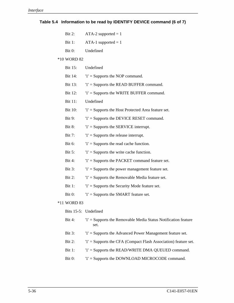
Interface
5-36 C141-E057-01EN
Table 5.4 Information to be read by IDENTIFY DEVICE command (6 of 7)
Bit 2: ATA-2 supported = 1
Bit 1: ATA-1 supported = 1
Bit 0: Undefined
*10 WORD 82
Bit 15: Undefined
Bit 14: '1' = Supports the NOP command.
Bit 13: '1' = Supports the READ BUFFER command.
Bit 12: '1' = Supports the WRITE BUFFER command.
Bit 11: Undefined
Bit 10: '1' = Supports the Host Protected Area feature set.
Bit 9: '1' = Supports the DEVICE RESET command.
Bit 8: '1' = Supports the SERVICE interrupt.
Bit 7: '1' = Supports the release interrupt.
Bit 6: '1' = Supports the read cache function.
Bit 5: '1' = Supports the write cache function.
Bit 4: '1' = Supports the PACKET command feature set.
Bit 3: '1' = Supports the power management feature set.
Bit 2: '1' = Supports the Removable Media feature set.
Bit 1: '1' = Supports the Security Mode feature set.
Bit 0: '1' = Supports the SMART feature set.
*11 WORD 83
Bits 15-5: Undefined
Bit 4: '1' = Supports the Removable Media Status Notification feature set.
Bit 3: '1' = Supports the Advanced Power Management feature set.
Bit 2: '1' = Supports the CFA (Compact Flash Association) feature set.
Bit 1: '1' = Supports the READ/WRITE DMA QUEUED command.
Bit 0: '1' = Supports the DOWNLOAD MICROCODE command.
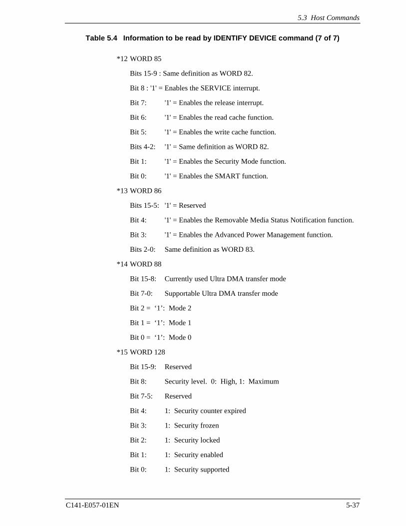
5.3 Host Commands
C141-E057-01EN 5-37
Table 5.4 Information to be read by IDENTIFY DEVICE command (7 of 7)
*12 WORD 85
Bits 15-9 : Same definition as WORD 82.
Bit 8 : '1' = Enables the SERVICE interrupt.
Bit 7: '1' = Enables the release interrupt.
Bit 6: '1' = Enables the read cache function.
Bit 5: '1' = Enables the write cache function.
Bits 4-2: '1' = Same definition as WORD 82.
Bit 1: '1' = Enables the Security Mode function.
Bit 0: '1' = Enables the SMART function.
*13 WORD 86
Bits 15-5: '1' = Reserved
Bit 4: '1' = Enables the Removable Media Status Notification function.
Bit 3: '1' = Enables the Advanced Power Management function.
Bits 2-0: Same definition as WORD 83.
*14 WORD 88
Bit 15-8: Currently used Ultra DMA transfer mode
Bit 7-0: Supportable Ultra DMA transfer mode
Bit 2 = ‘1’: Mode 2
Bit 1 = ‘1’: Mode 1
Bit 0 = ‘1’: Mode 0
*15 WORD 128
Bit 15-9: Reserved
Bit 8: Security level. 0: High, 1: Maximum
Bit 7-5: Reserved
Bit 4: 1: Security counter expired
Bit 3: 1: Security frozen
Bit 2: 1: Security locked
Bit 1: 1: Security enabled
Bit 0: 1: Security supported
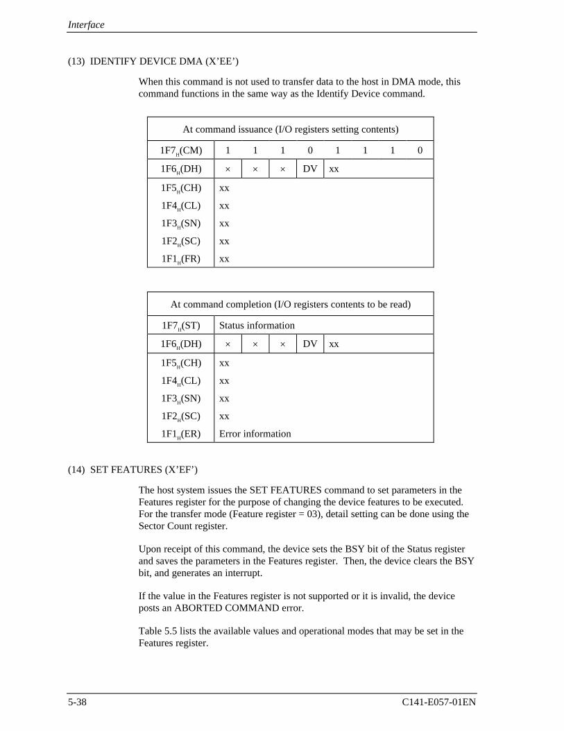
Interface
5-38 C141-E057-01EN
(13) IDENTIFY DEVICE DMA (X’EE’)
When this command is not used to transfer data to the host in DMA mode, thiscommand functions in the same way as the Identify Device command.
At command issuance (I/O registers setting contents)
1F7H(CM) 1 1 1 0 1 1 1 0
1F6H(DH) × × × DV xx
1F5H(CH)
1F4H(CL)
1F3H(SN)
1F2H(SC)
1F1H(FR)
xx
xx
xx
xx
xx
At command completion (I/O registers contents to be read)
1F7H(ST) Status information
1F6H(DH) × × × DV xx
1F5H(CH)
1F4H(CL)
1F3H(SN)
1F2H(SC)
1F1H(ER)
xx
xx
xx
xx
Error information
(14) SET FEATURES (X’EF’)
The host system issues the SET FEATURES command to set parameters in theFeatures register for the purpose of changing the device features to be executed.For the transfer mode (Feature register = 03), detail setting can be done using theSector Count register.
Upon receipt of this command, the device sets the BSY bit of the Status registerand saves the parameters in the Features register. Then, the device clears the BSYbit, and generates an interrupt.
If the value in the Features register is not supported or it is invalid, the deviceposts an ABORTED COMMAND error.
Table 5.5 lists the available values and operational modes that may be set in theFeatures register.
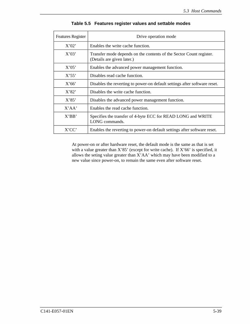
5.3 Host Commands
C141-E057-01EN 5-39
Table 5.5 Features register values and settable modes
Features Register Drive operation mode
X’02’ Enables the write cache function.
X’03’ Transfer mode depends on the contents of the Sector Count register.(Details are given later.)
X’05’ Enables the advanced power management function.
X’55’ Disables read cache function.
X’66’ Disables the reverting to power-on default settings after software reset.
X’82’ Disables the write cache function.
X’85’ Disables the advanced power management function.
X’AA’ Enables the read cache function.
X’BB’ Specifies the transfer of 4-byte ECC for READ LONG and WRITELONG commands.
X’CC’ Enables the reverting to power-on default settings after software reset.
At power-on or after hardware reset, the default mode is the same as that is setwith a value greater than X’85’ (except for write cache). If X’66’ is specified, itallows the seting value greater than X’AA’ which may have been modified to anew value since power-on, to remain the same even after software reset.
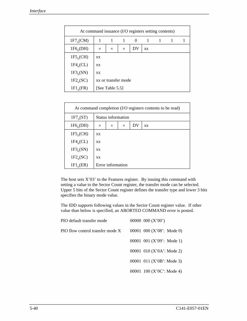
Interface
5-40 C141-E057-01EN
At command issuance (I/O registers setting contents)
1F7H(CM) 1 1 1 0 1 1 1 1
1F6H(DH) × × × DV xx
1F5H(CH)
1F4H(CL)
1F3H(SN)
1F2H(SC)
1F1H(FR)
xx
xx
xx
xx or transfer mode
[See Table 5.5]
At command completion (I/O registers contents to be read)
1F7H(ST) Status information
1F6H(DH) × × × DV xx
1F5H(CH)
1F4H(CL)
1F3H(SN)
1F2H(SC)
1F1H(ER)
xx
xx
xx
xx
Error information
The host sets X’03’ to the Features register. By issuing this command withsetting a value to the Sector Count register, the transfer mode can be selected.Upper 5 bits of the Sector Count register defines the transfer type and lower 3 bitsspecifies the binary mode value.
The IDD supports following values in the Sector Count register value. If othervalue than below is specified, an ABORTED COMMAND error is posted.
PIO default transfer mode 00000 000 (X’00’)
PIO flow control transfer mode X 00001 000 (X’08’: Mode 0)
00001 001 (X’09’: Mode 1)
00001 010 (X’0A’: Mode 2)
00001 011 (X’0B’: Mode 3)
00001 100 (X’0C’: Mode 4)
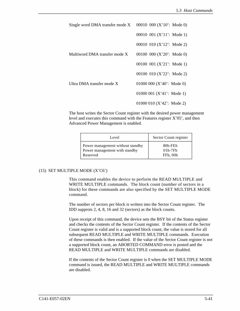
5.3 Host Commands
C141-E057-02EN 5-41
Single word DMA transfer mode X 00010 000 (X’10’: Mode 0)
00010 001 (X’11’: Mode 1)
00010 010 (X’12’: Mode 2)
Multiword DMA transfer mode X 00100 000 (X’20’: Mode 0)
00100 001 (X’21’: Mode 1)
00100 010 (X’22’: Mode 2)
Ultra DMA transfer mode X 01000 000 (X’40’: Mode 0)
01000 001 (X’41’: Mode 1)
01000 010 (X’42’: Mode 2)
The host writes the Sector Count register with the desired power managementlevel and executes this command with the Features register X’05’, and thenAdvanced Power Management is enabled.
Level Sector Count register
Power management without standbyPower management with standbyReserved
80h-FEh01h-7FhFFh, 00h
(15) SET MULTIPLE MODE (X’C6’)
This command enables the device to perform the READ MULTIPLE andWRITE MULTIPLE commands. The block count (number of sectors in ablock) for these commands are also specified by the SET MULTIPLE MODEcommand.
The number of sectors per block is written into the Sector Count register. TheIDD supprots 2, 4, 8, 16 and 32 (sectors) as the block counts.
Upon receipt of this command, the device sets the BSY bit of the Status registerand checks the contents of the Sector Count register. If the contents of the SectorCount register is valid and is a supported block count, the value is stored for allsubsequent READ MULTIPLE and WRITE MULTIPLE commands. Executionof these commands is then enabled. If the value of the Sector Count register is nota supported block count, an ABORTED COMMAND error is posted and theREAD MULTIPLE and WRITE MULTIPLE commands are disabled.
If the contents of the Sector Count register is 0 when the SET MULTIPLE MODEcommand is issued, the READ MULTIPLE and WRITE MULTIPLE commandsare disabled.
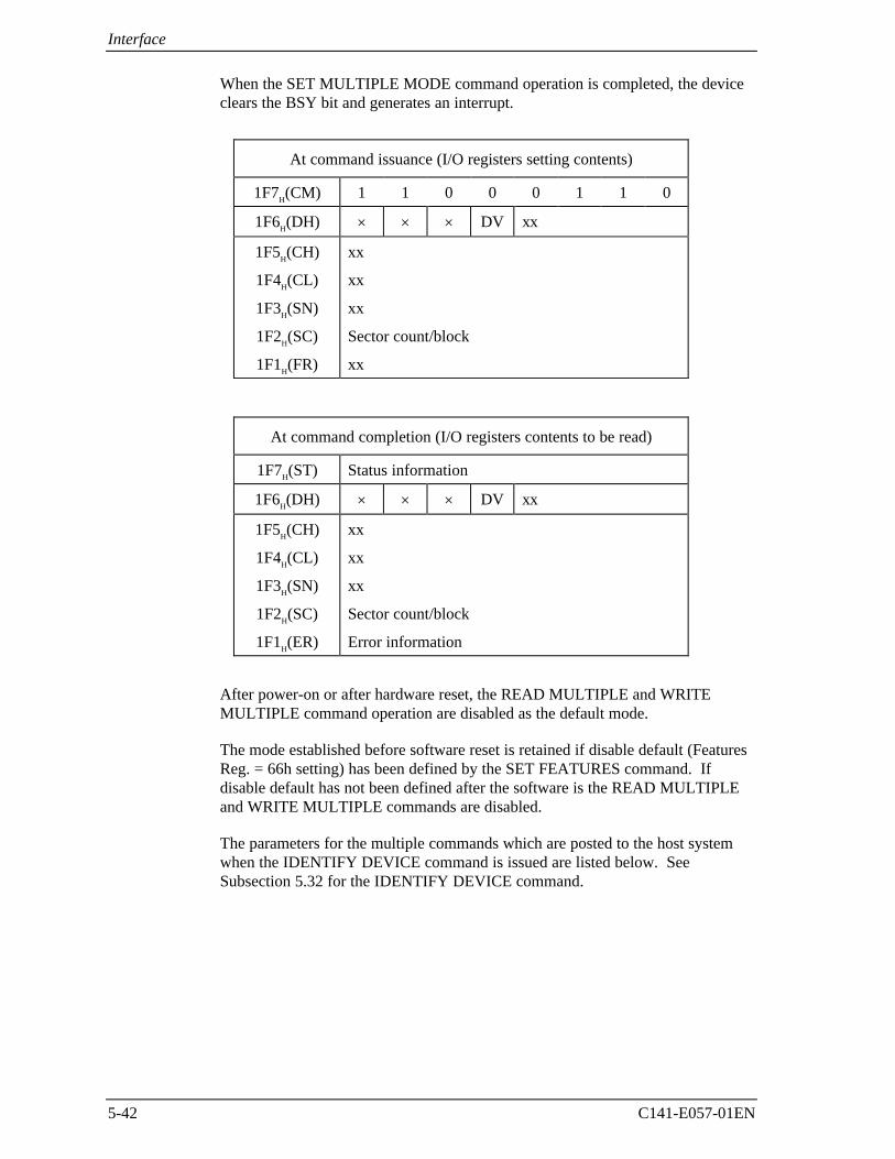
Interface
5-42 C141-E057-01EN
When the SET MULTIPLE MODE command operation is completed, the deviceclears the BSY bit and generates an interrupt.
At command issuance (I/O registers setting contents)
1F7H(CM) 1 1 0 0 0 1 1 0
1F6H(DH) × × × DV xx
1F5H(CH)
1F4H(CL)
1F3H(SN)
1F2H(SC)
1F1H(FR)
xx
xx
xx
Sector count/block
xx
At command completion (I/O registers contents to be read)
1F7H(ST) Status information
1F6H(DH) × × × DV xx
1F5H(CH)
1F4H(CL)
1F3H(SN)
1F2H(SC)
1F1H(ER)
xx
xx
xx
Sector count/block
Error information
After power-on or after hardware reset, the READ MULTIPLE and WRITEMULTIPLE command operation are disabled as the default mode.
The mode established before software reset is retained if disable default (FeaturesReg. = 66h setting) has been defined by the SET FEATURES command. Ifdisable default has not been defined after the software is the READ MULTIPLEand WRITE MULTIPLE commands are disabled.
The parameters for the multiple commands which are posted to the host systemwhen the IDENTIFY DEVICE command is issued are listed below. SeeSubsection 5.32 for the IDENTIFY DEVICE command.
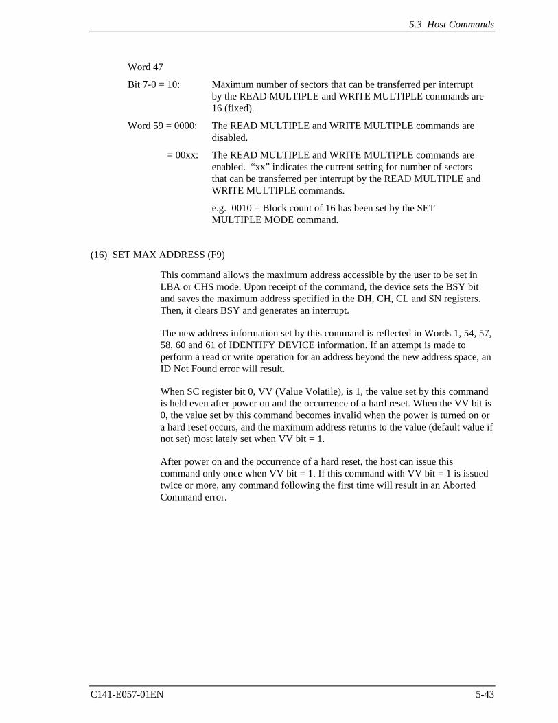
5.3 Host Commands
C141-E057-01EN 5-43
Word 47
Bit 7-0 = 10:
Word 59 = 0000:
= 00xx:
Maximum number of sectors that can be transferred per interruptby the READ MULTIPLE and WRITE MULTIPLE commands are16 (fixed).
The READ MULTIPLE and WRITE MULTIPLE commands aredisabled.
The READ MULTIPLE and WRITE MULTIPLE commands areenabled. “xx” indicates the current setting for number of sectorsthat can be transferred per interrupt by the READ MULTIPLE andWRITE MULTIPLE commands.
e.g. 0010 = Block count of 16 has been set by the SETMULTIPLE MODE command.
(16) SET MAX ADDRESS (F9)
This command allows the maximum address accessible by the user to be set inLBA or CHS mode. Upon receipt of the command, the device sets the BSY bitand saves the maximum address specified in the DH, CH, CL and SN registers.Then, it clears BSY and generates an interrupt.
The new address information set by this command is reflected in Words 1, 54, 57,58, 60 and 61 of IDENTIFY DEVICE information. If an attempt is made toperform a read or write operation for an address beyond the new address space, anID Not Found error will result.
When SC register bit 0, VV (Value Volatile), is 1, the value set by this commandis held even after power on and the occurrence of a hard reset. When the VV bit is0, the value set by this command becomes invalid when the power is turned on ora hard reset occurs, and the maximum address returns to the value (default value ifnot set) most lately set when VV bit = 1.
After power on and the occurrence of a hard reset, the host can issue thiscommand only once when VV bit = 1. If this command with VV bit = 1 is issuedtwice or more, any command following the first time will result in an AbortedCommand error.
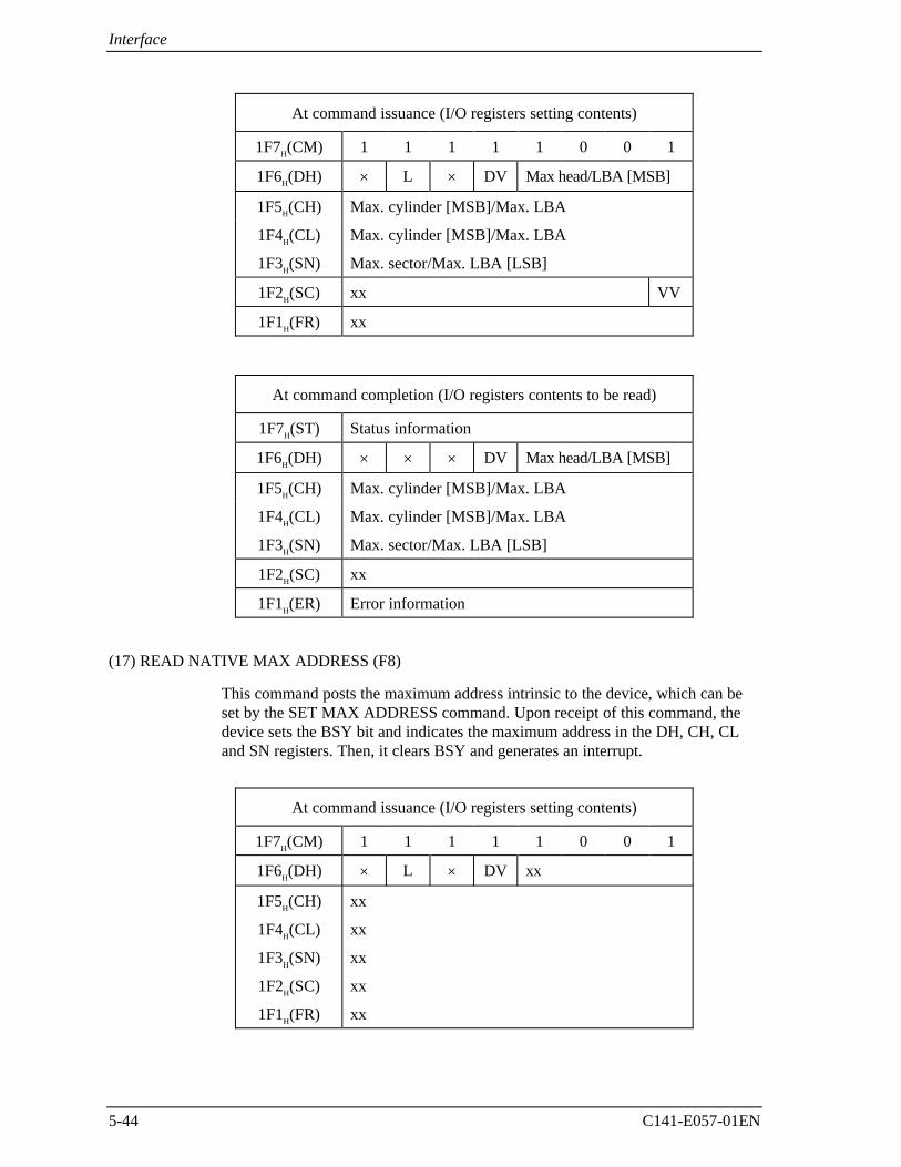
Interface
5-44 C141-E057-01EN
At command issuance (I/O registers setting contents)
1F7H(CM) 1 1 1 1 1 0 0 1
1F6H(DH) × L × DV Max head/LBA [MSB]
1F5H(CH) Max. cylinder [MSB]/Max. LBA
1F4H(CL) Max. cylinder [MSB]/Max. LBA
1F3H(SN) Max. sector/Max. LBA [LSB]
1F2H(SC) xx VV
1F1H(FR) xx
At command completion (I/O registers contents to be read)
1F7H(ST) Status information
1F6H(DH) × × × DV Max head/LBA [MSB]
1F5H(CH) Max. cylinder [MSB]/Max. LBA
1F4H(CL) Max. cylinder [MSB]/Max. LBA
1F3H(SN) Max. sector/Max. LBA [LSB]
1F2H(SC) xx
1F1H(ER) Error information
(17) READ NATIVE MAX ADDRESS (F8)
This command posts the maximum address intrinsic to the device, which can beset by the SET MAX ADDRESS command. Upon receipt of this command, thedevice sets the BSY bit and indicates the maximum address in the DH, CH, CLand SN registers. Then, it clears BSY and generates an interrupt.
At command issuance (I/O registers setting contents)
1F7H(CM) 1 1 1 1 1 0 0 1
1F6H(DH) × L × DV xx
1F5H(CH)
1F4H(CL)
1F3H(SN)
1F2H(SC)
1F1H(FR)
xx
xx
xx
xx
xx
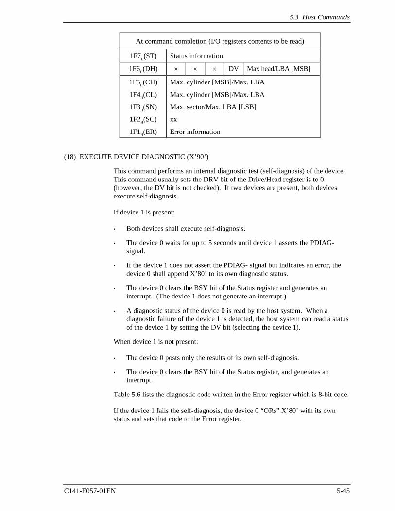
5.3 Host Commands
C141-E057-01EN 5-45
At command completion (I/O registers contents to be read)
1F7H(ST) Status information
1F6H(DH) × × × DV Max head/LBA [MSB]
1F5H(CH)
1F4H(CL)
1F3H(SN)
1F2H(SC)
1F1H(ER)
Max. cylinder [MSB]/Max. LBA
Max. cylinder [MSB]/Max. LBA
Max. sector/Max. LBA [LSB]
xx
Error information
(18) EXECUTE DEVICE DIAGNOSTIC (X’90’)
This command performs an internal diagnostic test (self-diagnosis) of the device.This command usually sets the DRV bit of the Drive/Head register is to 0(however, the DV bit is not checked). If two devices are present, both devicesexecute self-diagnosis.
If device 1 is present:
• Both devices shall execute self-diagnosis.
• The device 0 waits for up to 5 seconds until device 1 asserts the PDIAG-signal.
• If the device 1 does not assert the PDIAG- signal but indicates an error, thedevice 0 shall append X’80’ to its own diagnostic status.
• The device 0 clears the BSY bit of the Status register and generates aninterrupt. (The device 1 does not generate an interrupt.)
• A diagnostic status of the device 0 is read by the host system. When adiagnostic failure of the device 1 is detected, the host system can read a statusof the device 1 by setting the DV bit (selecting the device 1).
When device 1 is not present:
• The device 0 posts only the results of its own self-diagnosis.
• The device 0 clears the BSY bit of the Status register, and generates aninterrupt.
Table 5.6 lists the diagnostic code written in the Error register which is 8-bit code.
If the device 1 fails the self-diagnosis, the device 0 “ORs” X’80’ with its ownstatus and sets that code to the Error register.
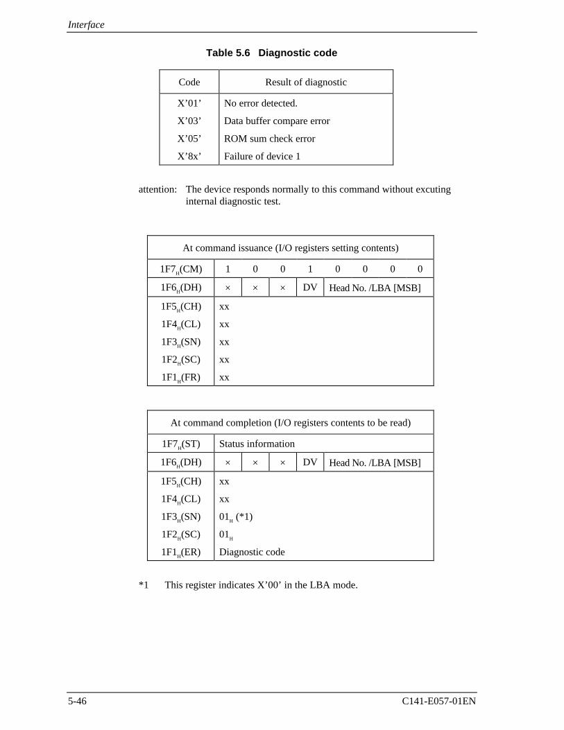
Interface
5-46 C141-E057-01EN
Table 5.6 Diagnostic code
Code Result of diagnostic
X’01’
X’03’
X’05’
X’8x’
No error detected.
Data buffer compare error
ROM sum check error
Failure of device 1
attention: The device responds normally to this command without excutinginternal diagnostic test.
At command issuance (I/O registers setting contents)
1F7H(CM) 1 0 0 1 0 0 0 0
1F6H(DH) × × × DV Head No. /LBA [MSB]
1F5H(CH)
1F4H(CL)
1F3H(SN)
1F2H(SC)
1F1H(FR)
xx
xx
xx
xx
xx
At command completion (I/O registers contents to be read)
1F7H(ST) Status information
1F6H(DH) × × × DV Head No. /LBA [MSB]
1F5H(CH)
1F4H(CL)
1F3H(SN)
1F2H(SC)
1F1H(ER)
xx
xx
01H (*1)
01H
Diagnostic code
*1 This register indicates X’00’ in the LBA mode.
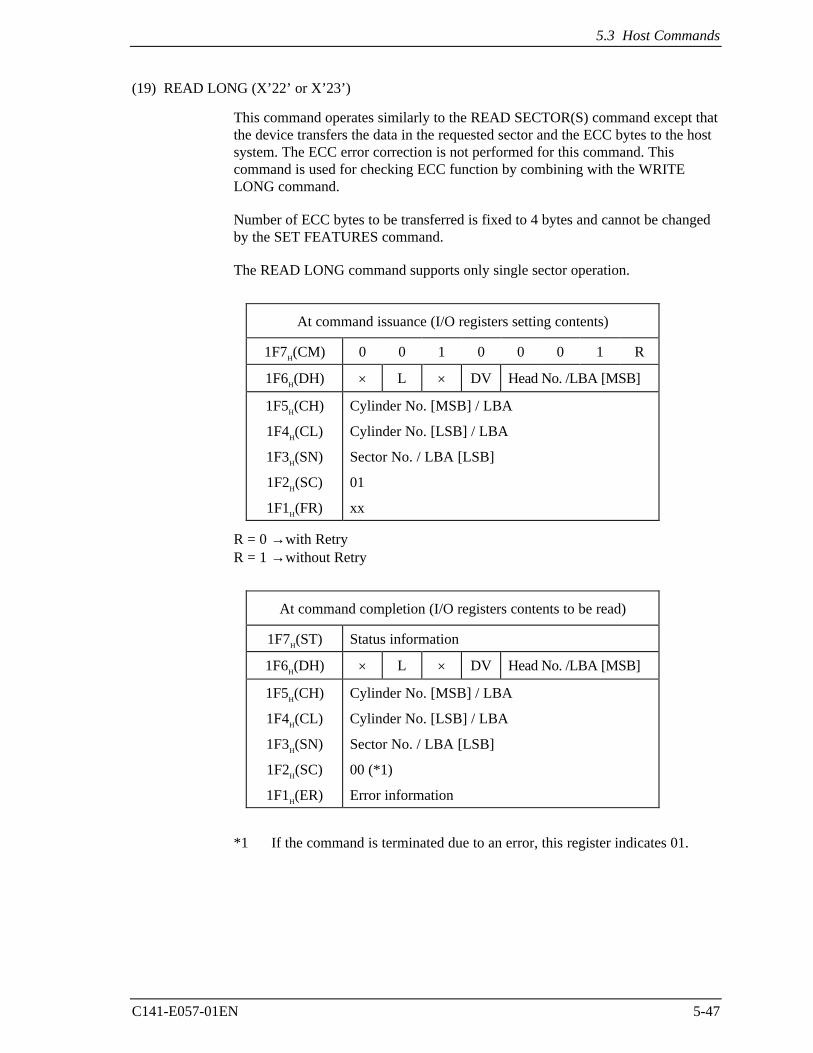
5.3 Host Commands
C141-E057-01EN 5-47
(19) READ LONG (X’22’ or X’23’)
This command operates similarly to the READ SECTOR(S) command except thatthe device transfers the data in the requested sector and the ECC bytes to the hostsystem. The ECC error correction is not performed for this command. Thiscommand is used for checking ECC function by combining with the WRITELONG command.
Number of ECC bytes to be transferred is fixed to 4 bytes and cannot be changedby the SET FEATURES command.
The READ LONG command supports only single sector operation.
At command issuance (I/O registers setting contents)
1F7H(CM) 0 0 1 0 0 0 1 R
1F6H(DH) × L × DV Head No. /LBA [MSB]
1F5H(CH)
1F4H(CL)
1F3H(SN)
1F2H(SC)
1F1H(FR)
Cylinder No. [MSB] / LBA
Cylinder No. [LSB] / LBA
Sector No. / LBA [LSB]
01
xx
R = 0 →with RetryR = 1 →without Retry
At command completion (I/O registers contents to be read)
1F7H(ST) Status information
1F6H(DH) × L × DV Head No. /LBA [MSB]
1F5H(CH)
1F4H(CL)
1F3H(SN)
1F2H(SC)
1F1H(ER)
Cylinder No. [MSB] / LBA
Cylinder No. [LSB] / LBA
Sector No. / LBA [LSB]
00 (*1)
Error information
*1 If the command is terminated due to an error, this register indicates 01.
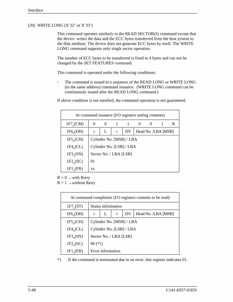
Interface
5-48 C141-E057-01EN
(20) WRITE LONG (X’32’ or X’33’)
This command operates similarly to the READ SECTOR(S) command except thatthe device writes the data and the ECC bytes transferred from the host system tothe disk medium. The device does not generate ECC bytes by itself. The WRITELONG command supports only single sector operation.
The number of ECC bytes to be transferred is fixed to 4 bytes and can not bechanged by the SET FEATURES command.
This command is operated under the following conditions:
• The command is issued in a sequence of the READ LONG or WRITE LONG(to the same address) command issuance. (WRITE LONG command can becontinuously issued after the READ LONG command.)
If above condition is not satisfied, the command operation is not guaranteed.
At command issuance (I/O registers setting contents)
1F7H(CM) 0 0 1 1 0 0 1 R
1F6H(DH) × L × DV Head No. /LBA [MSB]
1F5H(CH)
1F4H(CL)
1F3H(SN)
1F2H(SC)
1F1H(FR)
Cylinder No. [MSB] / LBA
Cylinder No. [LSB] / LBA
Sector No. / LBA [LSB]
01
xx
R = 0 →with RetryR = 1 →without Retry
At command completion (I/O registers contents to be read)
1F7H(ST) Status information
1F6H(DH) × L × DV Head No. /LBA [MSB]
1F5H(CH)
1F4H(CL)
1F3H(SN)
1F2H(SC)
1F1H(ER)
Cylinder No. [MSB] / LBA
Cylinder No. [LSB] / LBA
Sector No. / LBA [LSB]
00 (*1)
Error information
*1 If the command is terminated due to an error, this register indicates 01.
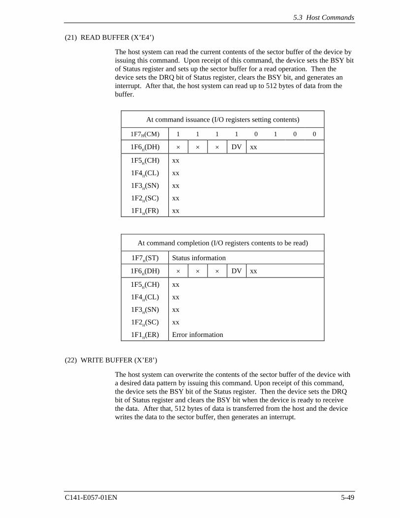
5.3 Host Commands
C141-E057-01EN 5-49
(21) READ BUFFER (X’E4’)
The host system can read the current contents of the sector buffer of the device byissuing this command. Upon receipt of this command, the device sets the BSY bitof Status register and sets up the sector buffer for a read operation. Then thedevice sets the DRQ bit of Status register, clears the BSY bit, and generates aninterrupt. After that, the host system can read up to 512 bytes of data from thebuffer.
At command issuance (I/O registers setting contents)
1F7H(CM) 1 1 1 1 0 1 0 0
1F6H(DH) × × × DV xx
1F5H(CH)
1F4H(CL)
1F3H(SN)
1F2H(SC)
1F1H(FR)
xx
xx
xx
xx
xx
At command completion (I/O registers contents to be read)
1F7H(ST) Status information
1F6H(DH) × × × DV xx
1F5H(CH)
1F4H(CL)
1F3H(SN)
1F2H(SC)
1F1H(ER)
xx
xx
xx
xx
Error information
(22) WRITE BUFFER (X’E8’)
The host system can overwrite the contents of the sector buffer of the device witha desired data pattern by issuing this command. Upon receipt of this command,the device sets the BSY bit of the Status register. Then the device sets the DRQbit of Status register and clears the BSY bit when the device is ready to receivethe data. After that, 512 bytes of data is transferred from the host and the devicewrites the data to the sector buffer, then generates an interrupt.
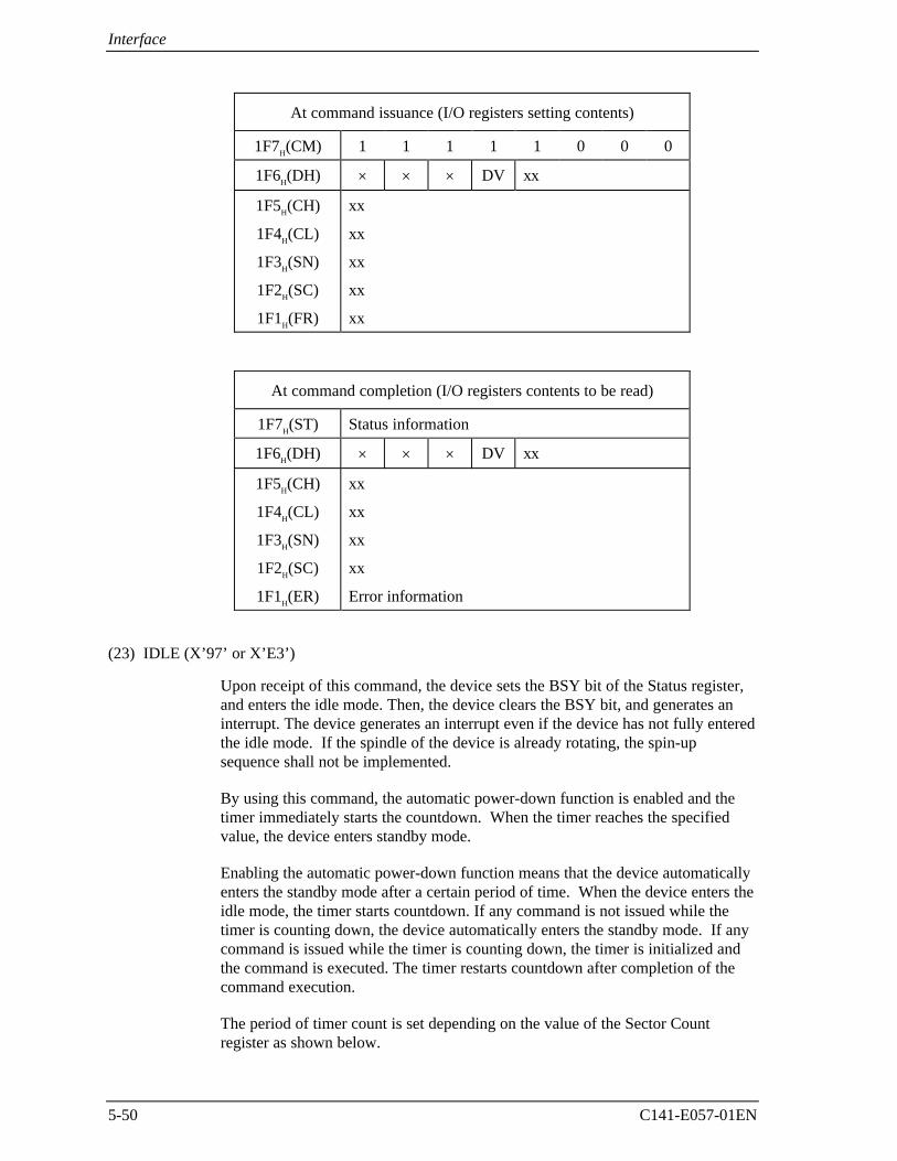
Interface
5-50 C141-E057-01EN
At command issuance (I/O registers setting contents)
1F7H(CM) 1 1 1 1 1 0 0 0
1F6H(DH) × × × DV xx
1F5H(CH)
1F4H(CL)
1F3H(SN)
1F2H(SC)
1F1H(FR)
xx
xx
xx
xx
xx
At command completion (I/O registers contents to be read)
1F7H(ST) Status information
1F6H(DH) × × × DV xx
1F5H(CH)
1F4H(CL)
1F3H(SN)
1F2H(SC)
1F1H(ER)
xx
xx
xx
xx
Error information
(23) IDLE (X’97’ or X’E3’)
Upon receipt of this command, the device sets the BSY bit of the Status register,and enters the idle mode. Then, the device clears the BSY bit, and generates aninterrupt. The device generates an interrupt even if the device has not fully enteredthe idle mode. If the spindle of the device is already rotating, the spin-upsequence shall not be implemented.
By using this command, the automatic power-down function is enabled and thetimer immediately starts the countdown. When the timer reaches the specifiedvalue, the device enters standby mode.
Enabling the automatic power-down function means that the device automaticallyenters the standby mode after a certain period of time. When the device enters theidle mode, the timer starts countdown. If any command is not issued while thetimer is counting down, the device automatically enters the standby mode. If anycommand is issued while the timer is counting down, the timer is initialized andthe command is executed. The timer restarts countdown after completion of thecommand execution.
The period of timer count is set depending on the value of the Sector Countregister as shown below.
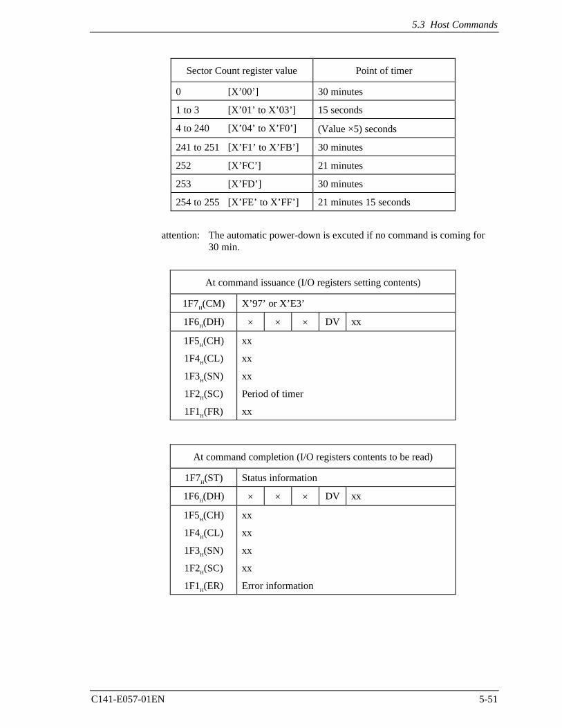
5.3 Host Commands
C141-E057-01EN 5-51
Sector Count register value Point of timer
0 [X’00’] 30 minutes
1 to 3 [X’01’ to X’03’] 15 seconds
4 to 240 [X’04’ to X’F0’] (Value ×5) seconds
241 to 251 [X’F1’ to X’FB’] 30 minutes
252 [X’FC’] 21 minutes
253 [X’FD’] 30 minutes
254 to 255 [X’FE’ to X’FF’] 21 minutes 15 seconds
attention: The automatic power-down is excuted if no command is coming for30 min.
At command issuance (I/O registers setting contents)
1F7H(CM) X’97’ or X’E3’
1F6H(DH) × × × DV xx
1F5H(CH)
1F4H(CL)
1F3H(SN)
1F2H(SC)
1F1H(FR)
xx
xx
xx
Period of timer
xx
At command completion (I/O registers contents to be read)
1F7H(ST) Status information
1F6H(DH) × × × DV xx
1F5H(CH)
1F4H(CL)
1F3H(SN)
1F2H(SC)
1F1H(ER)
xx
xx
xx
xx
Error information
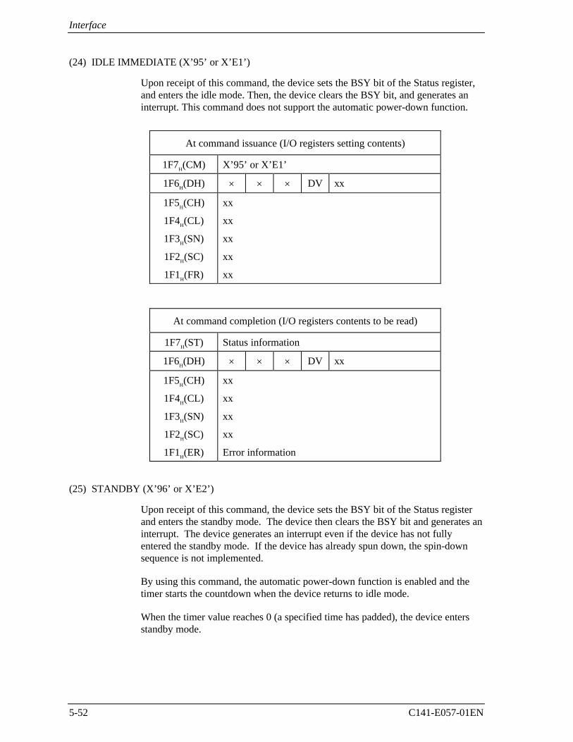
Interface
5-52 C141-E057-01EN
(24) IDLE IMMEDIATE (X’95’ or X’E1’)
Upon receipt of this command, the device sets the BSY bit of the Status register,and enters the idle mode. Then, the device clears the BSY bit, and generates aninterrupt. This command does not support the automatic power-down function.
At command issuance (I/O registers setting contents)
1F7H(CM) X’95’ or X’E1’
1F6H(DH) × × × DV xx
1F5H(CH)
1F4H(CL)
1F3H(SN)
1F2H(SC)
1F1H(FR)
xx
xx
xx
xx
xx
At command completion (I/O registers contents to be read)
1F7H(ST) Status information
1F6H(DH) × × × DV xx
1F5H(CH)
1F4H(CL)
1F3H(SN)
1F2H(SC)
1F1H(ER)
xx
xx
xx
xx
Error information
(25) STANDBY (X’96’ or X’E2’)
Upon receipt of this command, the device sets the BSY bit of the Status registerand enters the standby mode. The device then clears the BSY bit and generates aninterrupt. The device generates an interrupt even if the device has not fullyentered the standby mode. If the device has already spun down, the spin-downsequence is not implemented.
By using this command, the automatic power-down function is enabled and thetimer starts the countdown when the device returns to idle mode.
When the timer value reaches 0 (a specified time has padded), the device entersstandby mode.
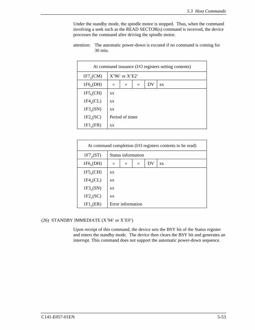
5.3 Host Commands
C141-E057-01EN 5-53
Under the standby mode, the spindle motor is stopped. Thus, when the commandinvolving a seek such as the READ SECTOR(s) command is received, the deviceprocesses the command after driving the spindle motor.
attention: The automatic power-down is excuted if no command is coming for30 min.
At command issuance (I/O registers setting contents)
1F7H(CM) X’96’ or X’E2’
1F6H(DH) × × × DV xx
1F5H(CH)
1F4H(CL)
1F3H(SN)
1F2H(SC)
1F1H(FR)
xx
xx
xx
Period of timer
xx
At command completion (I/O registers contents to be read)
1F7H(ST) Status information
1F6H(DH) × × × DV xx
1F5H(CH)
1F4H(CL)
1F3H(SN)
1F2H(SC)
1F1H(ER)
xx
xx
xx
xx
Error information
(26) STANDBY IMMEDIATE (X’94’ or X’E0’)
Upon receipt of this command, the device sets the BSY bit of the Status registerand enters the standby mode. The device then clears the BSY bit and generates aninterrupt. This command does not support the automatic power-down sequence.
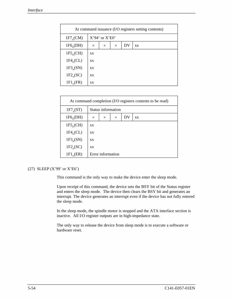
Interface
5-54 C141-E057-01EN
At command issuance (I/O registers setting contents)
1F7H(CM) X’94’ or X’E0’
1F6H(DH) × × × DV xx
1F5H(CH)
1F4H(CL)
1F3H(SN)
1F2H(SC)
1F1H(FR)
xx
xx
xx
xx
xx
At command completion (I/O registers contents to be read)
1F7H(ST) Status information
1F6H(DH) × × × DV xx
1F5H(CH)
1F4H(CL)
1F3H(SN)
1F2H(SC)
1F1H(ER)
xx
xx
xx
xx
Error information
(27) SLEEP (X’99’ or X’E6’)
This command is the only way to make the device enter the sleep mode.
Upon receipt of this command, the device sets the BSY bit of the Status registerand enters the sleep mode. The device then clears the BSY bit and generates aninterrupt. The device generates an interrupt even if the device has not fully enteredthe sleep mode.
In the sleep mode, the spindle motor is stopped and the ATA interface section isinactive. All I/O register outputs are in high-impedance state.
The only way to release the device from sleep mode is to execute a software orhardware reset.
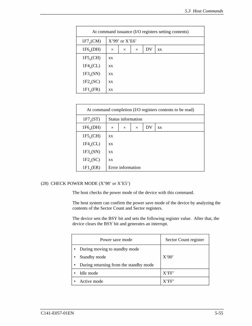
5.3 Host Commands
C141-E057-01EN 5-55
At command issuance (I/O registers setting contents)
1F7H(CM) X’99’ or X’E6’
1F6H(DH) × × × DV xx
1F5H(CH)
1F4H(CL)
1F3H(SN)
1F2H(SC)
1F1H(FR)
xx
xx
xx
xx
xx
At command completion (I/O registers contents to be read)
1F7H(ST) Status information
1F6H(DH) × × × DV xx
1F5H(CH)
1F4H(CL)
1F3H(SN)
1F2H(SC)
1F1H(ER)
xx
xx
xx
xx
Error information
(28) CHECK POWER MODE (X’98’ or X’E5’)
The host checks the power mode of the device with this command.
The host system can confirm the power save mode of the device by analyzing thecontents of the Sector Count and Sector registers.
The device sets the BSY bit and sets the following register value. After that, thedevice clears the BSY bit and generates an interrupt.
Power save mode Sector Count register
• During moving to standby mode
• Standby mode
• During returning from the standby mode
X’00’
• Idle mode X’FF’
• Active mode X’FF’
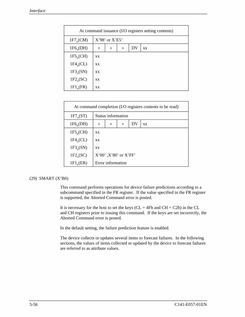
Interface
5-56 C141-E057-01EN
At command issuance (I/O registers setting contents)
1F7H(CM) X’98’ or X’E5’
1F6H(DH) × × × DV xx
1F5H(CH)
1F4H(CL)
1F3H(SN)
1F2H(SC)
1F1H(FR)
xx
xx
xx
xx
xx
At command completion (I/O registers contents to be read)
1F7H(ST) Status information
1F6H(DH) × × × DV xx
1F5H(CH)
1F4H(CL)
1F3H(SN)
1F2H(SC)
1F1H(ER)
xx
xx
xx
X’00’ ,X’80’ or X’FF’
Error information
(29) SMART (X’B0)
This command performs operations for device failure predictions according to asubcommand specified in the FR register. If the value specified in the FR registeris supported, the Aborted Command error is posted.
It is necessary for the host to set the keys (CL = 4Fh and CH = C2h) in the CLand CH registers prior to issuing this command. If the keys are set incorrectly, theAborted Command error is posted.
In the default setting, the failure prediction feature is enabled.
The device collects or updates several items to forecast failures. In the followingsections, the values of items collected or updated by the device to forecast failuresare referred to as attribute values.
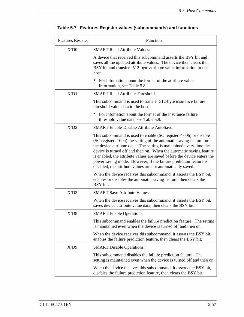
5.3 Host Commands
C141-E057-01EN 5-57
Table 5.7 Features Register values (subcommands) and functions
Features Resister Function
X’D0’ SMART Read Attribute Values:
A device that received this subcommand asserts the BSY bit andsaves all the updated attribute values. The device then clears theBSY bit and transfers 512-byte attribute value information to thehost.
* For infomation about the format of the attribute valueinformation, see Table 5.8.
X’D1’ SMART Read Attribute Thresholds:
This subcommand is used to transfer 512-byte insurance failurethreshold value data to the host.
* For infomation about the format of the insurance failurethreshold value data, see Table 5.9.
X’D2’ SMART Enable-Disable Attribute AutoSave:
This subcommand is used to enable (SC register ≠ 00h) or disable(SC register = 00h) the setting of the automatic saving feature forthe device attribute data. The setting is maintained every time thedevice is turned off and then on. When the automatic saving featureis enabled, the attribute values are saved before the device enters thepower saving mode. However, if the failure prediction feature isdisabled, the attribute values are not automatically saved.
When the device receives this subcommand, it asserts the BSY bit,enables or disables the automatic saving feature, then clears theBSY bit.
X’D3’ SMART Save Attribute Values:
When the device receives this subcommand, it asserts the BSY bit,saves device attribute value data, then clears the BSY bit.
X’D8’ SMART Enable Operations:
This subcommand enables the failure prediction feature. The settingis maintained even when the device is turned off and then on.
When the device receives this subcommand, it asserts the BSY bit,enables the failure prediction feature, then clears the BSY bit.
X’D9’ SMART Disable Operations:
This subcommand disables the failure prediction feature. Thesetting is maintained even when the device is turned off and then on.
When the device receives this subcommand, it asserts the BSY bit,disables the failure prediction feature, then clears the BSY bit.
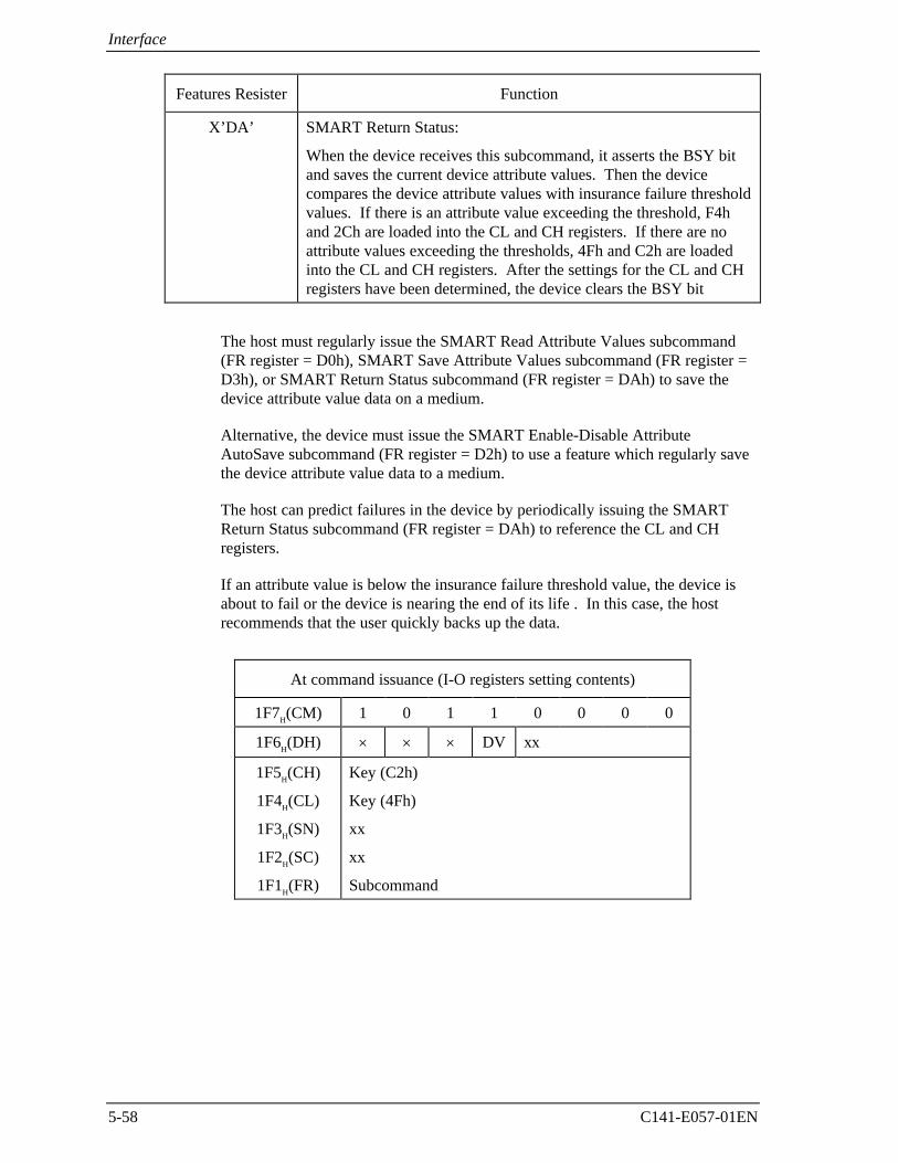
Interface
5-58 C141-E057-01EN
Features Resister Function
X’DA’ SMART Return Status:
When the device receives this subcommand, it asserts the BSY bitand saves the current device attribute values. Then the devicecompares the device attribute values with insurance failure thresholdvalues. If there is an attribute value exceeding the threshold, F4hand 2Ch are loaded into the CL and CH registers. If there are noattribute values exceeding the thresholds, 4Fh and C2h are loadedinto the CL and CH registers. After the settings for the CL and CHregisters have been determined, the device clears the BSY bit
The host must regularly issue the SMART Read Attribute Values subcommand(FR register = D0h), SMART Save Attribute Values subcommand (FR register =D3h), or SMART Return Status subcommand (FR register = DAh) to save thedevice attribute value data on a medium.
Alternative, the device must issue the SMART Enable-Disable AttributeAutoSave subcommand (FR register = D2h) to use a feature which regularly savethe device attribute value data to a medium.
The host can predict failures in the device by periodically issuing the SMARTReturn Status subcommand (FR register = DAh) to reference the CL and CHregisters.
If an attribute value is below the insurance failure threshold value, the device isabout to fail or the device is nearing the end of its life . In this case, the hostrecommends that the user quickly backs up the data.
At command issuance (I-O registers setting contents)
1F7H(CM) 1 0 1 1 0 0 0 0
1F6H(DH) × × × DV xx
1F5H(CH)
1F4H(CL)
1F3H(SN)
1F2H(SC)
1F1H(FR)
Key (C2h)
Key (4Fh)
xx
xx
Subcommand
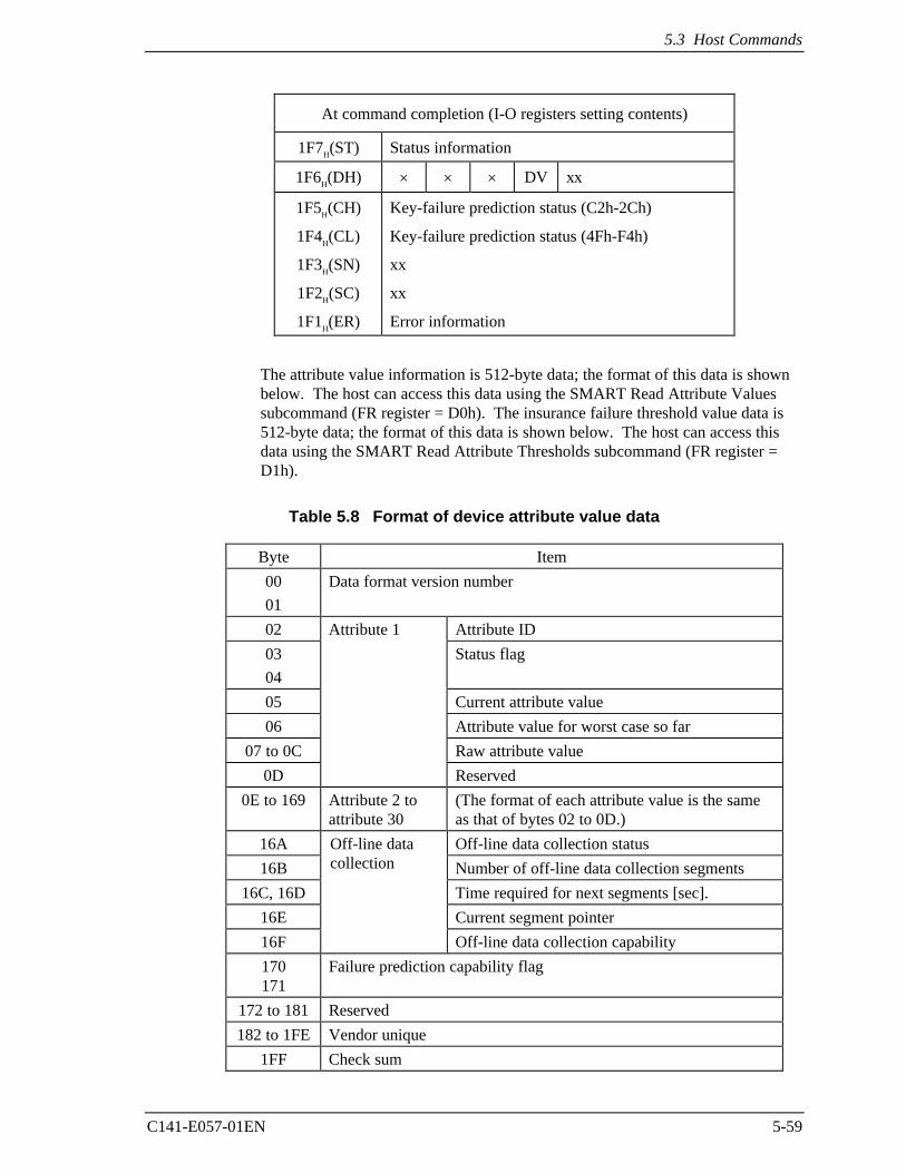
5.3 Host Commands
C141-E057-01EN 5-59
At command completion (I-O registers setting contents)
1F7H(ST) Status information
1F6H(DH) × × × DV xx
1F5H(CH)
1F4H(CL)
1F3H(SN)
1F2H(SC)
1F1H(ER)
Key-failure prediction status (C2h-2Ch)
Key-failure prediction status (4Fh-F4h)
xx
xx
Error information
The attribute value information is 512-byte data; the format of this data is shownbelow. The host can access this data using the SMART Read Attribute Valuessubcommand (FR register = D0h). The insurance failure threshold value data is512-byte data; the format of this data is shown below. The host can access thisdata using the SMART Read Attribute Thresholds subcommand (FR register =D1h).
Table 5.8 Format of device attribute value data
Byte Item
00
01
Data format version number
02 Attribute 1 Attribute ID
03
04
Status flag
05 Current attribute value
06 Attribute value for worst case so far
07 to 0C Raw attribute value
0D Reserved
0E to 169 Attribute 2 toattribute 30
(The format of each attribute value is the sameas that of bytes 02 to 0D.)
16A Off-line data collection status
16B Number of off-line data collection segments
16C, 16D Time required for next segments [sec].
16E Current segment pointer
16F Off-line data collection capability
170171
Failure prediction capability flag
172 to 181 Reserved
182 to 1FE Vendor unique
1FF Check sum
Off-line datacollection
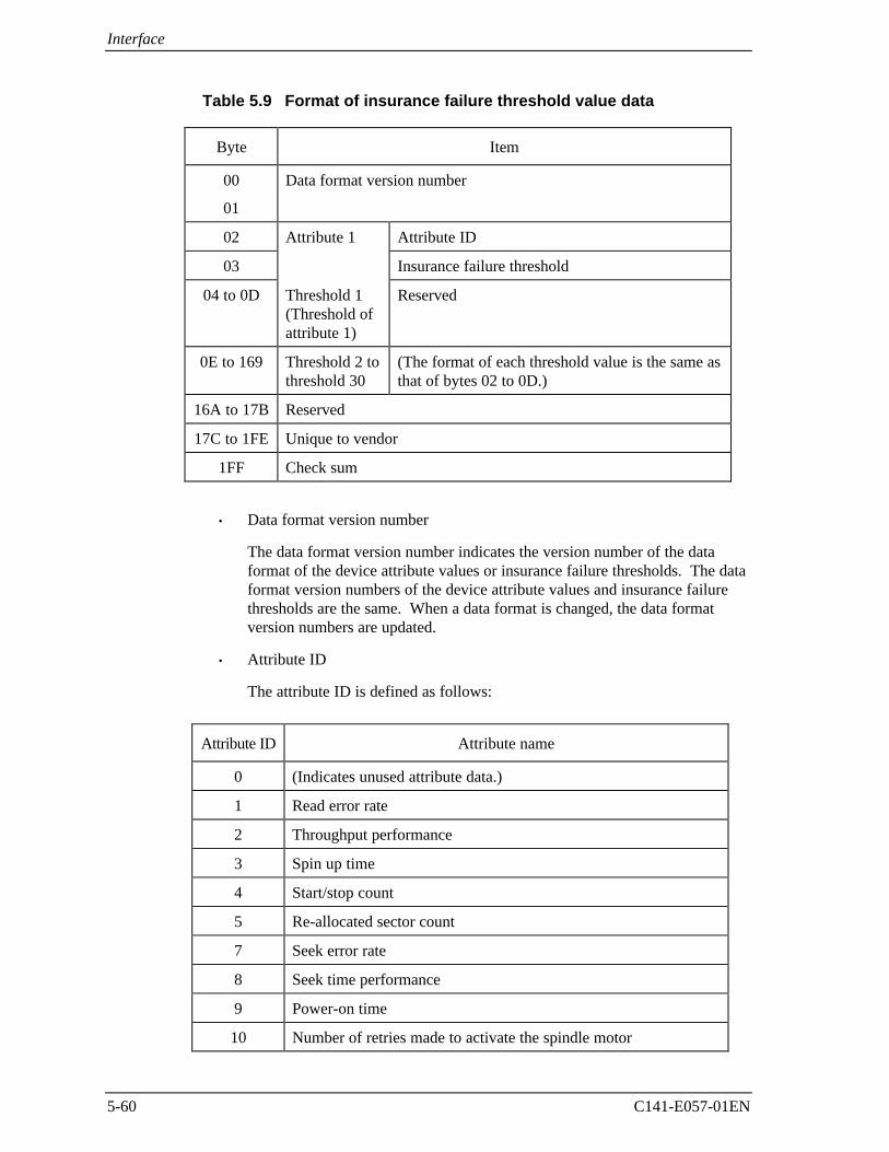
Interface
5-60 C141-E057-01EN
Table 5.9 Format of insurance failure threshold value data
Byte Item
00
01
Data format version number
02 Attribute 1 Attribute ID
03 Insurance failure threshold
04 to 0D Threshold 1(Threshold ofattribute 1)
Reserved
0E to 169 Threshold 2 tothreshold 30
(The format of each threshold value is the same asthat of bytes 02 to 0D.)
16A to 17B Reserved
17C to 1FE Unique to vendor
1FF Check sum
• Data format version number
The data format version number indicates the version number of the dataformat of the device attribute values or insurance failure thresholds. The dataformat version numbers of the device attribute values and insurance failurethresholds are the same. When a data format is changed, the data formatversion numbers are updated.
• Attribute ID
The attribute ID is defined as follows:
Attribute ID Attribute name
0 (Indicates unused attribute data.)
1 Read error rate
2 Throughput performance
3 Spin up time
4 Start/stop count
5 Re-allocated sector count
7 Seek error rate
8 Seek time performance
9 Power-on time
10 Number of retries made to activate the spindle motor
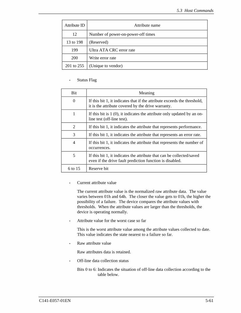
5.3 Host Commands
C141-E057-01EN 5-61
Attribute ID Attribute name
12 Number of power-on-power-off times
13 to 198 (Reserved)
199 Ultra ATA CRC error rate
200 Write error rate
201 to 255 (Unique to vendor)
• Status Flag
Bit Meaning
0 If this bit 1, it indicates that if the attribute exceeds the threshold,it is the attribute covered by the drive warranty.
1 If this bit is 1 (0), it indicates the attribute only updated by an on-line test (off-line test).
2 If this bit 1, it indicates the attribute that represents performance.
3 If this bit 1, it indicates the attribute that represents an error rate.
4 If this bit 1, it indicates the attribute that represents the number ofoccurrences.
5 If this bit 1, it indicates the attribute that can be collected/savedeven if the drive fault prediction function is disabled.
6 to 15 Reserve bit
• Current attribute value
The current attribute value is the normalized raw attribute data. The valuevaries between 01h and 64h. The closer the value gets to 01h, the higher thepossibility of a failure. The device compares the attribute values withthresholds. When the attribute values are larger than the thresholds, thedevice is operating normally.
• Attribute value for the worst case so far
This is the worst attribute value among the attribute values collected to date.This value indicates the state nearest to a failure so far.
• Raw attribute value
Raw attributes data is retained.
• Off-line data collection status
Bits 0 to 6: Indicates the situation of off-line data collection according to thetable below.
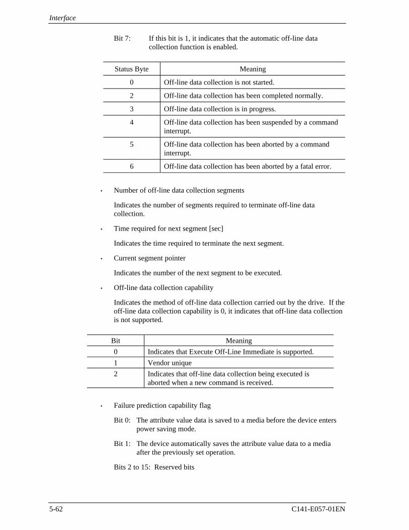
Interface
5-62 C141-E057-01EN
Bit 7: If this bit is 1, it indicates that the automatic off-line datacollection function is enabled.
Status Byte Meaning
0 Off-line data collection is not started.
2 Off-line data collection has been completed normally.
3 Off-line data collection is in progress.
4 Off-line data collection has been suspended by a commandinterrupt.
5 Off-line data collection has been aborted by a commandinterrupt.
6 Off-line data collection has been aborted by a fatal error.
• Number of off-line data collection segments
Indicates the number of segments required to terminate off-line datacollection.
• Time required for next segment [sec]
Indicates the time required to terminate the next segment.
• Current segment pointer
Indicates the number of the next segment to be executed.
• Off-line data collection capability
Indicates the method of off-line data collection carried out by the drive. If theoff-line data collection capability is 0, it indicates that off-line data collectionis not supported.
Bit Meaning
0 Indicates that Execute Off-Line Immediate is supported.
1 Vendor unique
2 Indicates that off-line data collection being executed isaborted when a new command is received.
• Failure prediction capability flag
Bit 0: The attribute value data is saved to a media before the device enterspower saving mode.
Bit 1: The device automatically saves the attribute value data to a mediaafter the previously set operation.
Bits 2 to 15: Reserved bits
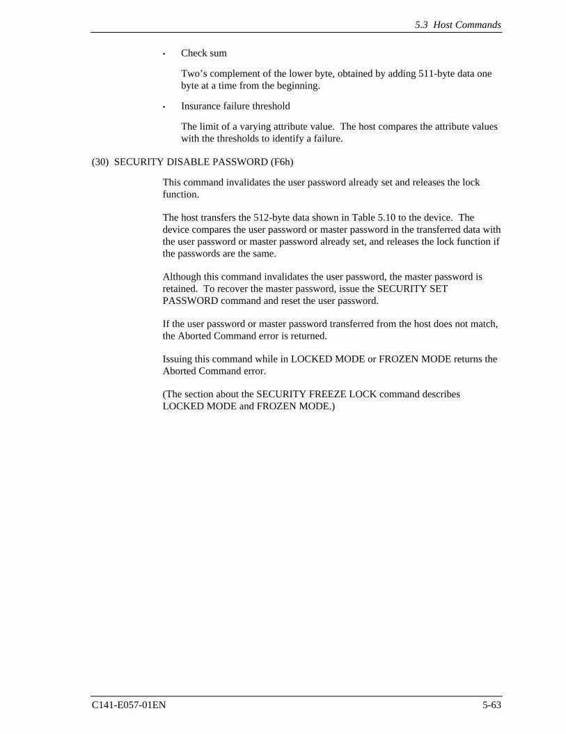
5.3 Host Commands
C141-E057-01EN 5-63
• Check sum
Two’s complement of the lower byte, obtained by adding 511-byte data onebyte at a time from the beginning.
• Insurance failure threshold
The limit of a varying attribute value. The host compares the attribute valueswith the thresholds to identify a failure.
(30) SECURITY DISABLE PASSWORD (F6h)
This command invalidates the user password already set and releases the lockfunction.
The host transfers the 512-byte data shown in Table 5.10 to the device. Thedevice compares the user password or master password in the transferred data withthe user password or master password already set, and releases the lock function ifthe passwords are the same.
Although this command invalidates the user password, the master password isretained. To recover the master password, issue the SECURITY SETPASSWORD command and reset the user password.
If the user password or master password transferred from the host does not match,the Aborted Command error is returned.
Issuing this command while in LOCKED MODE or FROZEN MODE returns theAborted Command error.
(The section about the SECURITY FREEZE LOCK command describesLOCKED MODE and FROZEN MODE.)
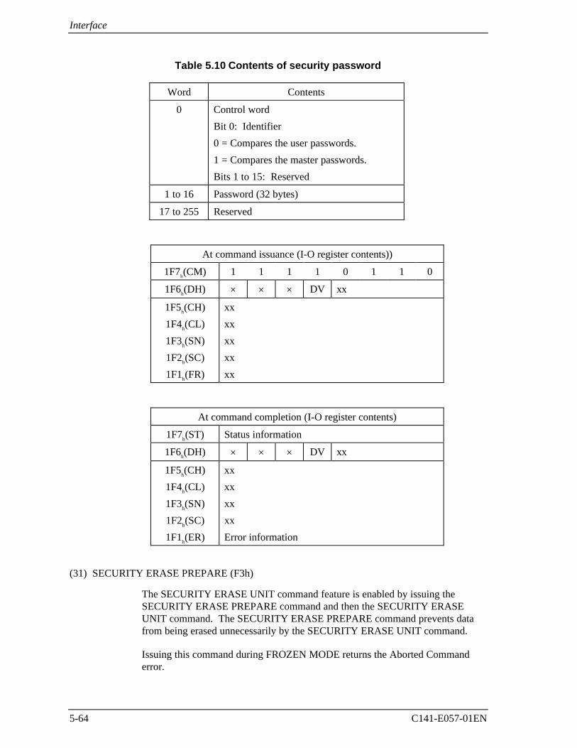
Interface
5-64 C141-E057-01EN
Table 5.10 Contents of security password
Word Contents
0 Control word
Bit 0: Identifier
0 = Compares the user passwords.
1 = Compares the master passwords.
Bits 1 to 15: Reserved
1 to 16 Password (32 bytes)
17 to 255 Reserved
At command issuance (I-O register contents))
1F7h(CM) 1 1 1 1 0 1 1 0
1F6h(DH) × × × DV xx
1F5h(CH)
1F4h(CL)
1F3h(SN)
1F2h(SC)
1F1h(FR)
xx
xx
xx
xx
xx
At command completion (I-O register contents)
1F7h(ST) Status information
1F6h(DH) × × × DV xx
1F5h(CH)
1F4h(CL)
1F3h(SN)
1F2h(SC)
1F1h(ER)
xx
xx
xx
xx
Error information
(31) SECURITY ERASE PREPARE (F3h)
The SECURITY ERASE UNIT command feature is enabled by issuing theSECURITY ERASE PREPARE command and then the SECURITY ERASEUNIT command. The SECURITY ERASE PREPARE command prevents datafrom being erased unnecessarily by the SECURITY ERASE UNIT command.
Issuing this command during FROZEN MODE returns the Aborted Commanderror.
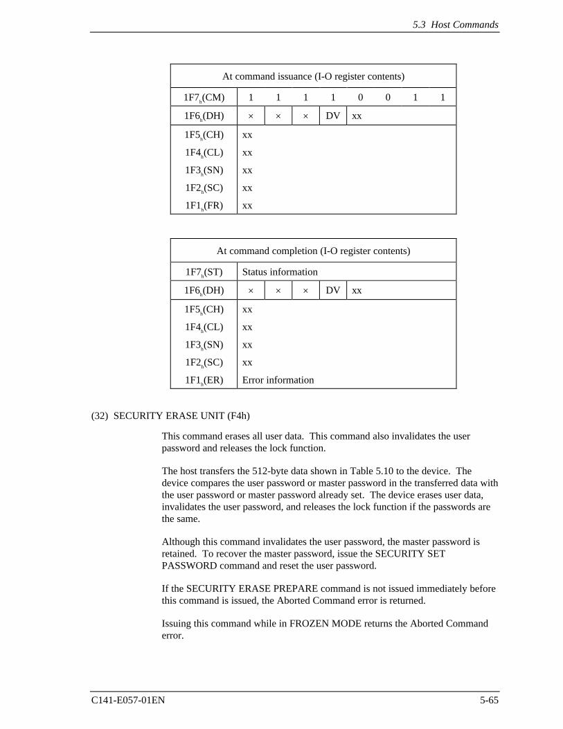
5.3 Host Commands
C141-E057-01EN 5-65
At command issuance (I-O register contents)
1F7h(CM) 1 1 1 1 0 0 1 1
1F6h(DH) × × × DV xx
1F5h(CH)
1F4h(CL)
1F3h(SN)
1F2h(SC)
1F1h(FR)
xx
xx
xx
xx
xx
At command completion (I-O register contents)
1F7h(ST) Status information
1F6h(DH) × × × DV xx
1F5h(CH)
1F4h(CL)
1F3h(SN)
1F2h(SC)
1F1h(ER)
xx
xx
xx
xx
Error information
(32) SECURITY ERASE UNIT (F4h)
This command erases all user data. This command also invalidates the userpassword and releases the lock function.
The host transfers the 512-byte data shown in Table 5.10 to the device. Thedevice compares the user password or master password in the transferred data withthe user password or master password already set. The device erases user data,invalidates the user password, and releases the lock function if the passwords arethe same.
Although this command invalidates the user password, the master password isretained. To recover the master password, issue the SECURITY SETPASSWORD command and reset the user password.
If the SECURITY ERASE PREPARE command is not issued immediately beforethis command is issued, the Aborted Command error is returned.
Issuing this command while in FROZEN MODE returns the Aborted Commanderror.
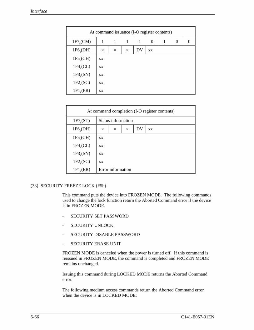
Interface
5-66 C141-E057-01EN
At command issuance (I-O register contents)
1F7h(CM) 1 1 1 1 0 1 0 0
1F6h(DH) × × × DV xx
1F5h(CH)
1F4h(CL)
1F3h(SN)
1F2h(SC)
1F1h(FR)
xx
xx
xx
xx
xx
At command completion (I-O register contents)
1F7h(ST) Status information
1F6h(DH) × × × DV xx
1F5h(CH)
1F4h(CL)
1F3h(SN)
1F2h(SC)
1F1h(ER)
xx
xx
xx
xx
Error information
(33) SECURITY FREEZE LOCK (F5h)
This command puts the device into FROZEN MODE. The following commandsused to change the lock function return the Aborted Command error if the deviceis in FROZEN MODE.
• SECURITY SET PASSWORD
• SECURITY UNLOCK
• SECURITY DISABLE PASSWORD
• SECURITY ERASE UNIT
FROZEN MODE is canceled when the power is turned off. If this command isreissued in FROZEN MODE, the command is completed and FROZEN MODEremains unchanged.
Issuing this command during LOCKED MODE returns the Aborted Commanderror.
The following medium access commands return the Aborted Command errorwhen the device is in LOCKED MODE:
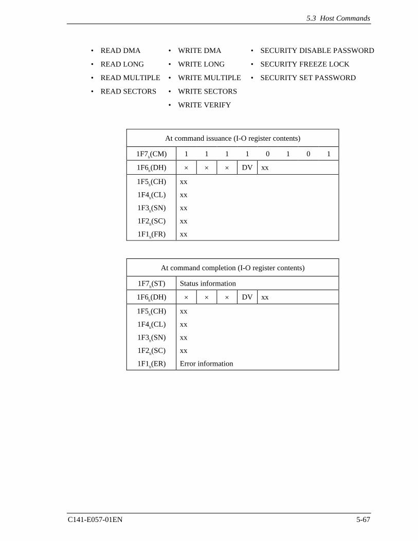
5.3 Host Commands
C141-E057-01EN 5-67
• READ DMA • WRITE DMA • SECURITY DISABLE PASSWORD
• READ LONG • WRITE LONG • SECURITY FREEZE LOCK
• READ MULTIPLE • WRITE MULTIPLE • SECURITY SET PASSWORD
• READ SECTORS • WRITE SECTORS
• WRITE VERIFY
At command issuance (I-O register contents)
1F7h(CM) 1 1 1 1 0 1 0 1
1F6h(DH) × × × DV xx
1F5h(CH)
1F4h(CL)
1F3h(SN)
1F2h(SC)
1F1h(FR)
xx
xx
xx
xx
xx
At command completion (I-O register contents)
1F7h(ST) Status information
1F6h(DH) × × × DV xx
1F5h(CH)
1F4h(CL)
1F3h(SN)
1F2h(SC)
1F1h(ER)
xx
xx
xx
xx
Error information
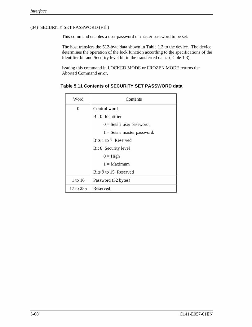
Interface
5-68 C141-E057-01EN
(34) SECURITY SET PASSWORD (F1h)
This command enables a user password or master password to be set.
The host transfers the 512-byte data shown in Table 1.2 to the device. The devicedetermines the operation of the lock function according to the specifications of theIdentifier bit and Security level bit in the transferred data. (Table 1.3)
Issuing this command in LOCKED MODE or FROZEN MODE returns theAborted Command error.
Table 5.11 Contents of SECURITY SET PASSWORD data
Word Contents
0 Control word
Bit 0 Identifier
0 = Sets a user password.
1 = Sets a master password.
Bits 1 to 7 Reserved
Bit 8 Security level
0 = High
1 = Maximum
Bits 9 to 15 Reserved
1 to 16 Password (32 bytes)
17 to 255 Reserved
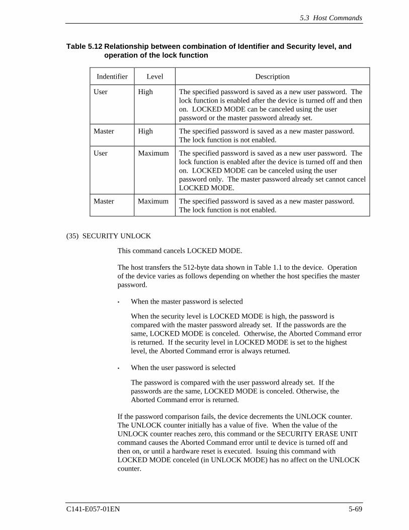
5.3 Host Commands
C141-E057-01EN 5-69
Table 5.12 Relationship between combination of Identifier and Security level, andoperation of the lock function
Indentifier Level Description
User High The specified password is saved as a new user password. Thelock function is enabled after the device is turned off and thenon. LOCKED MODE can be canceled using the userpassword or the master password already set.
Master High The specified password is saved as a new master password.The lock function is not enabled.
User Maximum The specified password is saved as a new user password. Thelock function is enabled after the device is turned off and thenon. LOCKED MODE can be canceled using the userpassword only. The master password already set cannot cancelLOCKED MODE.
Master Maximum The specified password is saved as a new master password.The lock function is not enabled.
(35) SECURITY UNLOCK
This command cancels LOCKED MODE.
The host transfers the 512-byte data shown in Table 1.1 to the device. Operationof the device varies as follows depending on whether the host specifies the masterpassword.
• When the master password is selected
When the security level is LOCKED MODE is high, the password iscompared with the master password already set. If the passwords are thesame, LOCKED MODE is conceled. Otherwise, the Aborted Command erroris returned. If the security level in LOCKED MODE is set to the highestlevel, the Aborted Command error is always returned.
• When the user password is selected
The password is compared with the user password already set. If thepasswords are the same, LOCKED MODE is conceled. Otherwise, theAborted Command error is returned.
If the password comparison fails, the device decrements the UNLOCK counter.The UNLOCK counter initially has a value of five. When the value of theUNLOCK counter reaches zero, this command or the SECURITY ERASE UNITcommand causes the Aborted Command error until te device is turned off andthen on, or until a hardware reset is executed. Issuing this command withLOCKED MODE conceled (in UNLOCK MODE) has no affect on the UNLOCKcounter.
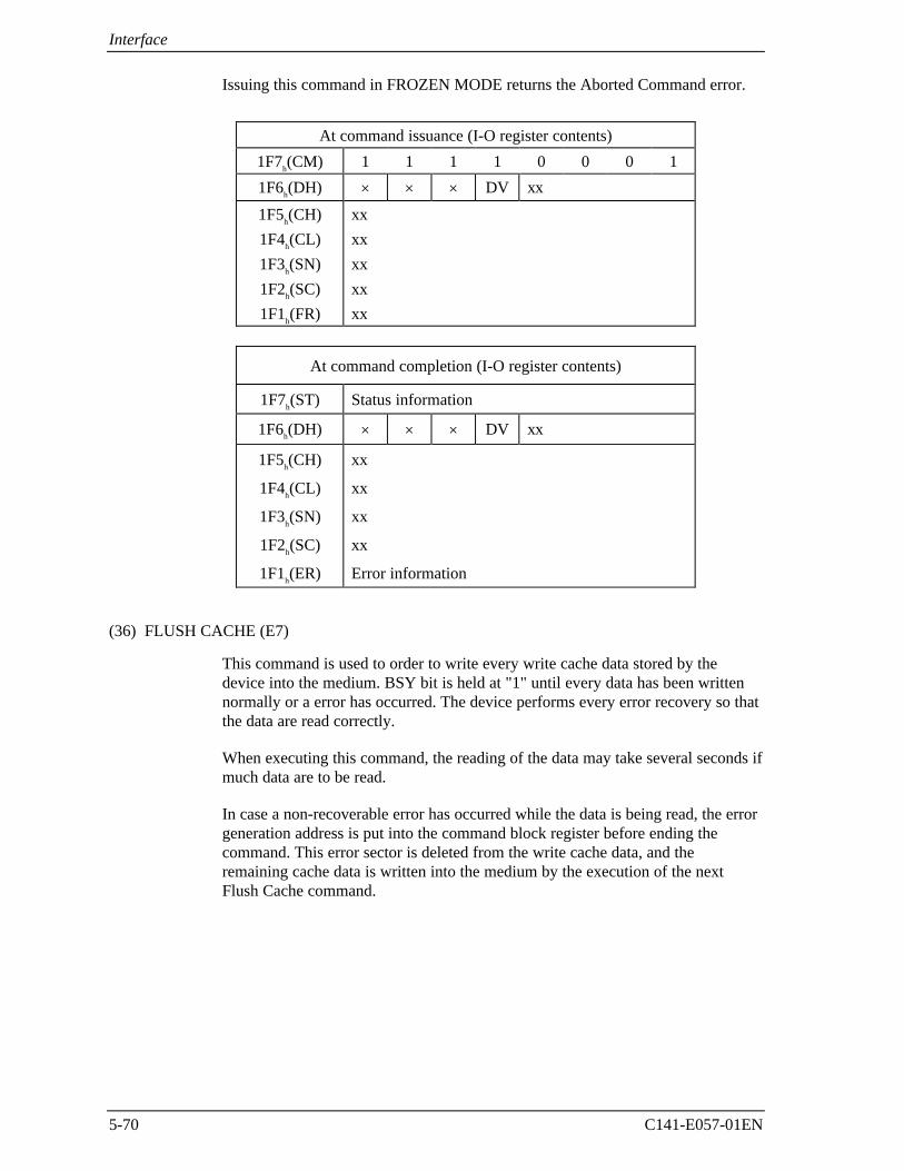
Interface
5-70 C141-E057-01EN
Issuing this command in FROZEN MODE returns the Aborted Command error.
At command issuance (I-O register contents)
1F7h(CM) 1 1 1 1 0 0 0 1
1F6h(DH) × × × DV xx
1F5h(CH)
1F4h(CL)
1F3h(SN)
1F2h(SC)
1F1h(FR)
xx
xx
xx
xx
xx
At command completion (I-O register contents)
1F7h(ST) Status information
1F6h(DH) × × × DV xx
1F5h(CH)
1F4h(CL)
1F3h(SN)
1F2h(SC)
1F1h(ER)
xx
xx
xx
xx
Error information
(36) FLUSH CACHE (E7)
This command is used to order to write every write cache data stored by thedevice into the medium. BSY bit is held at "1" until every data has been writtennormally or a error has occurred. The device performs every error recovery so thatthe data are read correctly.
When executing this command, the reading of the data may take several seconds ifmuch data are to be read.
In case a non-recoverable error has occurred while the data is being read, the errorgeneration address is put into the command block register before ending thecommand. This error sector is deleted from the write cache data, and theremaining cache data is written into the medium by the execution of the nextFlush Cache command.
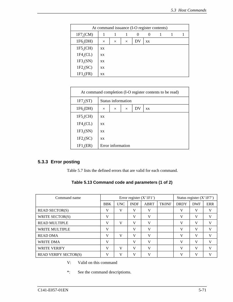
5.3 Host Commands
C141-E057-01EN 5-71
At command issuance (I-O register contents)
1F7h(CM) 1 1 1 0 0 1 1 1
1F6h(DH) × × × DV xx
1F5h(CH)
1F4h(CL)
1F3h(SN)
1F2h(SC)
1F1h(FR)
xx
xx
xx
xx
xx
At command completion (I-O register contents to be read)
1F7h(ST) Status information
1F6h(DH) × × × DV xx
1F5h(CH)
1F4h(CL)
1F3h(SN)
1F2h(SC)
1F1h(ER)
xx
xx
xx
xx
Error information
5.3.3 Error posting
Table 5.7 lists the defined errors that are valid for each command.
Table 5.13 Command code and parameters (1 of 2)
Command name Error register (X’1F1’) Status register (X’1F7’)
BBK UNC INDF ABRT TK0NF DRDY DWF ERR
READ SECTOR(S) V V V V V V V
WRITE SECTOR(S) V V V V V V
READ MULTIPLE V V V V V V V
WRITE MULTIPLE V V V V V V
READ DMA V V V V V V V
WRITE DMA V V V V V V
WRITE VERIFY V V V V V V V
READ VERIFY SECTOR(S) V V V V V V V
V: Valid on this command
*: See the command descriptioms.
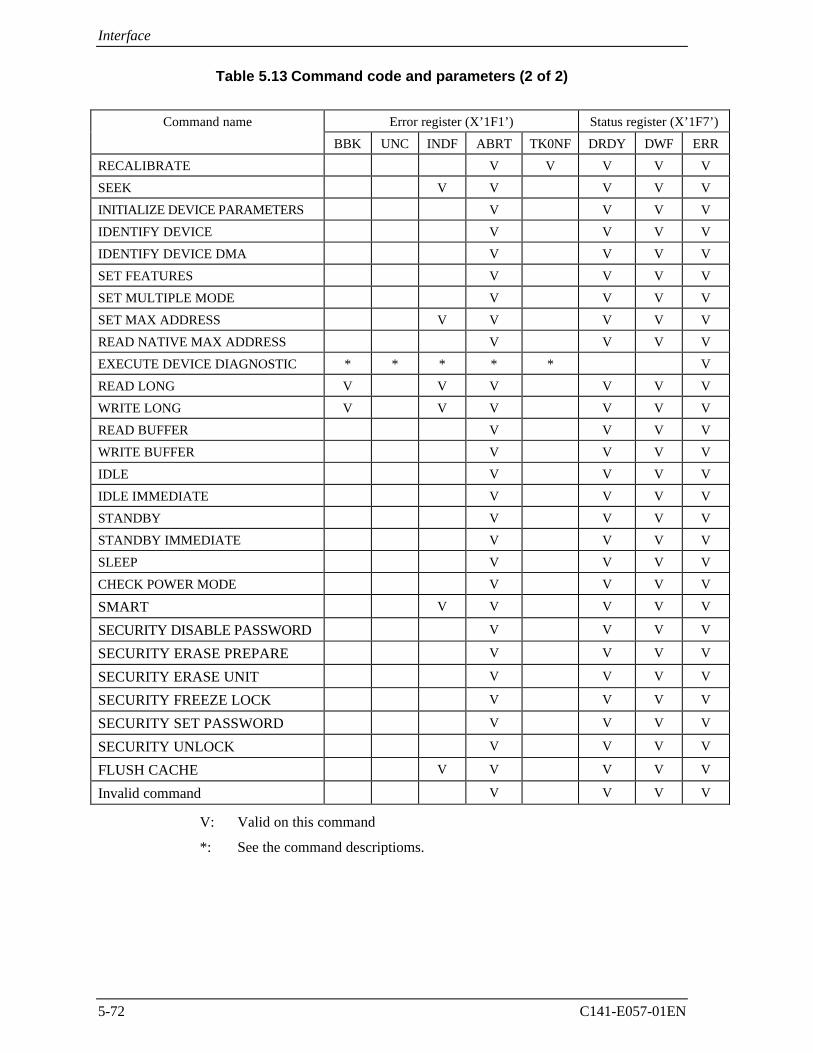
Interface
5-72 C141-E057-01EN
Table 5.13 Command code and parameters (2 of 2)
Command name Error register (X’1F1’) Status register (X’1F7’)
BBK UNC INDF ABRT TK0NF DRDY DWF ERR
RECALIBRATE V V V V V
SEEK V V V V V
INITIALIZE DEVICE PARAMETERS V V V V
IDENTIFY DEVICE V V V V
IDENTIFY DEVICE DMA V V V V
SET FEATURES V V V V
SET MULTIPLE MODE V V V V
SET MAX ADDRESS V V V V V
READ NATIVE MAX ADDRESS V V V V
EXECUTE DEVICE DIAGNOSTIC * * * * * V
READ LONG V V V V V V
WRITE LONG V V V V V V
READ BUFFER V V V V
WRITE BUFFER V V V V
IDLE V V V V
IDLE IMMEDIATE V V V V
STANDBY V V V V
STANDBY IMMEDIATE V V V V
SLEEP V V V V
CHECK POWER MODE V V V V
SMART V V V V V
SECURITY DISABLE PASSWORD V V V V
SECURITY ERASE PREPARE V V V V
SECURITY ERASE UNIT V V V V
SECURITY FREEZE LOCK V V V V
SECURITY SET PASSWORD V V V V
SECURITY UNLOCK V V V V
FLUSH CACHE V V V V V
Invalid command V V V V
V: Valid on this command
*: See the command descriptioms.
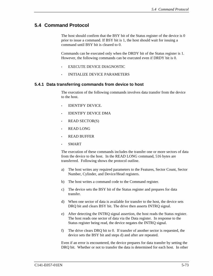
5.4 Command Protocol
C141-E057-01EN 5-73
5.4 Command Protocol
The host should confirm that the BSY bit of the Status register of the device is 0prior to issue a command. If BSY bit is 1, the host should wait for issuing acommand until BSY bit is cleared to 0.
Commands can be executed only when the DRDY bit of the Status register is 1.However, the following commands can be executed even if DRDY bit is 0.
• EXECUTE DEVICE DIAGNOSTIC
• INITIALIZE DEVICE PARAMETERS
5.4.1 Data transferring commands from device to host
The execution of the following commands involves data transfer from the deviceto the host.
• IDENTIFY DEVICE.
• IDENTIFY DEVICE DMA
• READ SECTOR(S)
• READ LONG
• READ BUFFER
• SMART
The execution of these commands includes the transfer one or more sectors of datafrom the device to the host. In the READ LONG command, 516 bytes aretransferred. Following shows the protocol outline.
a) The host writes any required parameters to the Features, Sector Count, SectorNumber, Cylinder, and Device/Head registers.
b) The host writes a command code to the Command register.
c) The device sets the BSY bit of the Status register and prepares for datatransfer.
d) When one sector of data is available for transfer to the host, the device setsDRQ bit and clears BSY bit. The drive then asserts INTRQ signal.
e) After detecting the INTRQ signal assertion, the host reads the Status register.The host reads one sector of data via the Data register. In response to theStatus register being read, the device negates the INTRQ signal.
f) The drive clears DRQ bit to 0. If transfer of another sector is requested, thedevice sets the BSY bit and steps d) and after are repeated.
Even if an error is encountered, the device prepares for data transfer by setting theDRQ bit. Whether or not to transfer the data is determined for each host. In other
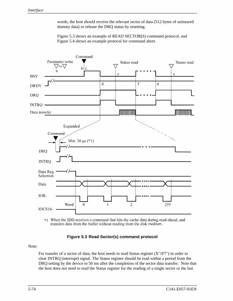
Interface
5-74 C141-E057-01EN
words, the host should receive the relevant sector of data (512 bytes of uninsureddummy data) or release the DRQ status by resetting.
Figure 5.3 shows an example of READ SECTOR(S) command protocol, andFigure 5.4 shows an example protocol for command abort.
Figure 5.3 Read Sector(s) command protocol
Note:
For transfer of a sector of data, the host needs to read Status register (X’1F7’) in order toclear INTRQ (interrupt) signal. The Status register should be read within a period from theDRQ setting by the device to 50 ms after the completion of the sector data transfer. Note thatthe host does not need to read the Status register for the reading of a single sector or the last
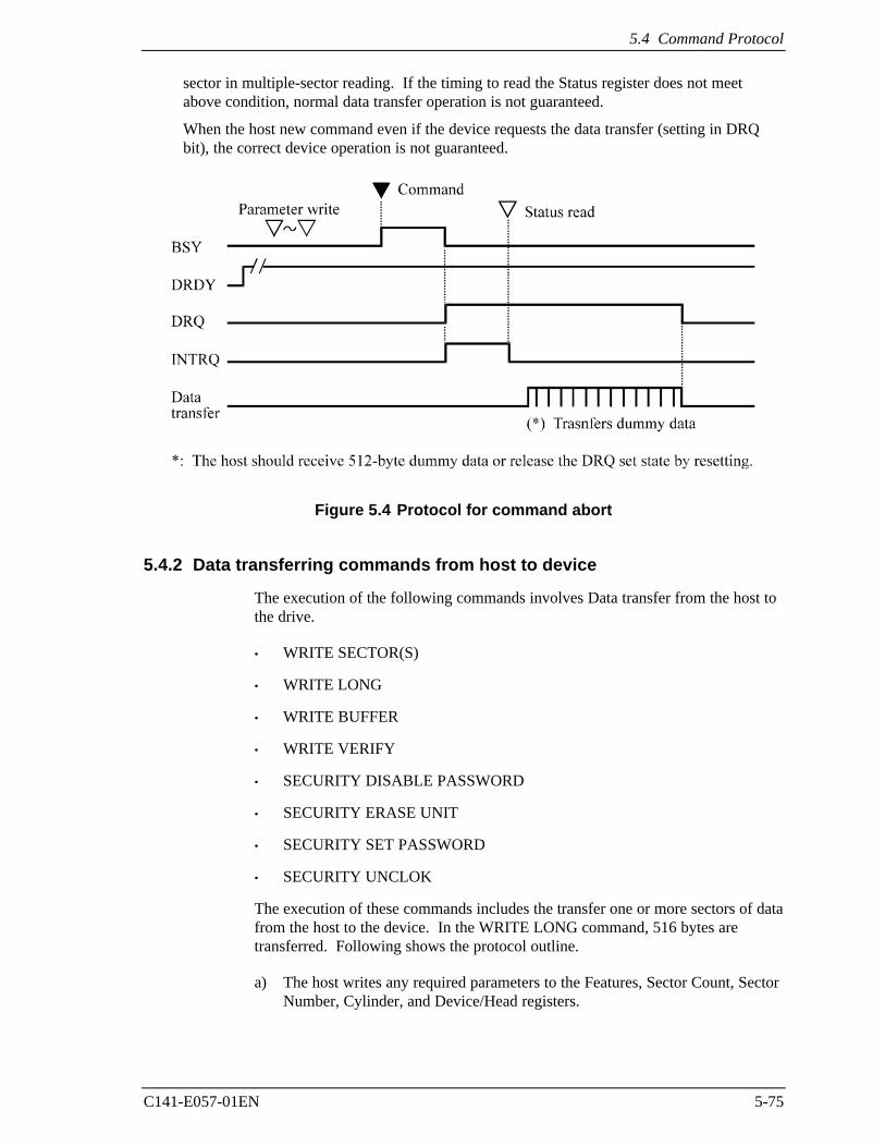
5.4 Command Protocol
C141-E057-01EN 5-75
sector in multiple-sector reading. If the timing to read the Status register does not meetabove condition, normal data transfer operation is not guaranteed.
When the host new command even if the device requests the data transfer (setting in DRQbit), the correct device operation is not guaranteed.
Figure 5.4 Protocol for command abort
5.4.2 Data transferring commands from host to device
The execution of the following commands involves Data transfer from the host tothe drive.
• WRITE SECTOR(S)
• WRITE LONG
• WRITE BUFFER
• WRITE VERIFY
• SECURITY DISABLE PASSWORD
• SECURITY ERASE UNIT
• SECURITY SET PASSWORD
• SECURITY UNCLOK
The execution of these commands includes the transfer one or more sectors of datafrom the host to the device. In the WRITE LONG command, 516 bytes aretransferred. Following shows the protocol outline.
a) The host writes any required parameters to the Features, Sector Count, SectorNumber, Cylinder, and Device/Head registers.
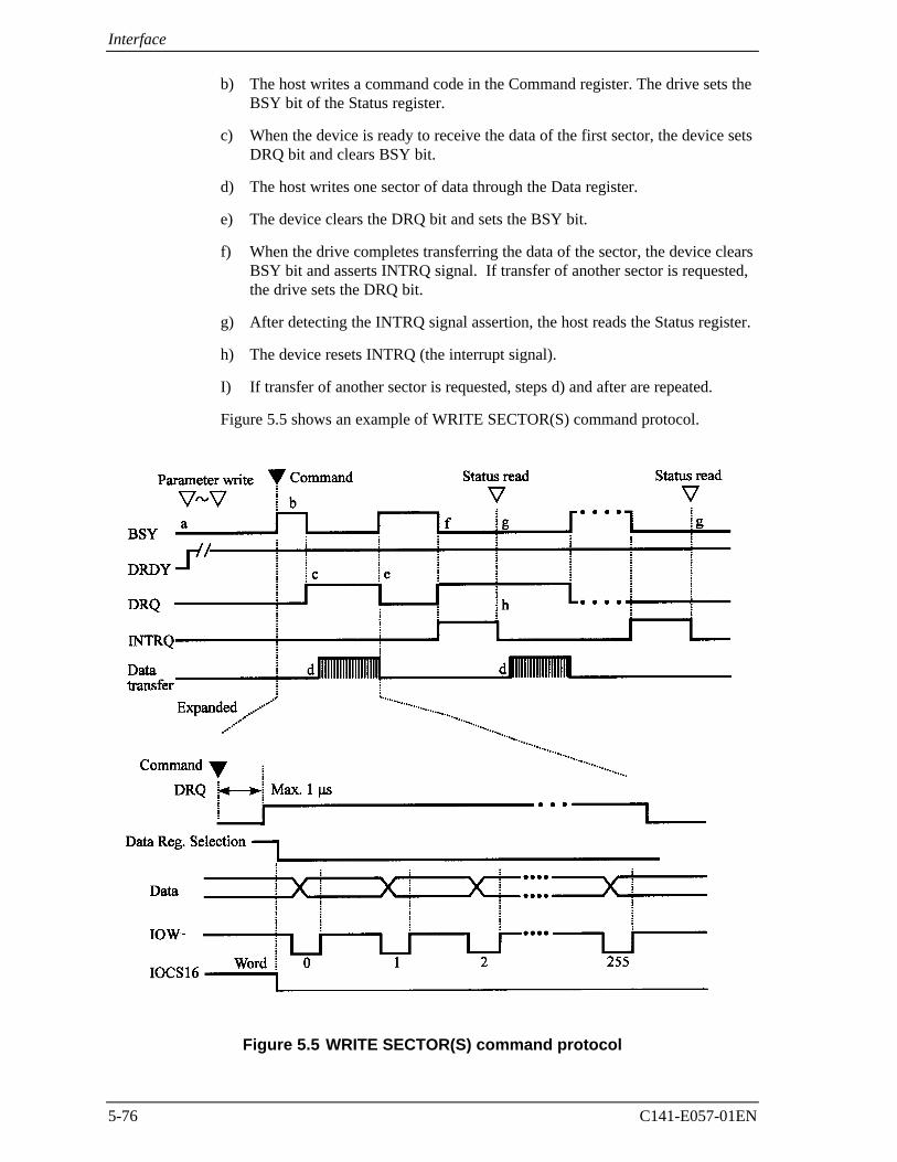
Interface
5-76 C141-E057-01EN
b) The host writes a command code in the Command register. The drive sets theBSY bit of the Status register.
c) When the device is ready to receive the data of the first sector, the device setsDRQ bit and clears BSY bit.
d) The host writes one sector of data through the Data register.
e) The device clears the DRQ bit and sets the BSY bit.
f) When the drive completes transferring the data of the sector, the device clearsBSY bit and asserts INTRQ signal. If transfer of another sector is requested,the drive sets the DRQ bit.
g) After detecting the INTRQ signal assertion, the host reads the Status register.
h) The device resets INTRQ (the interrupt signal).
I) If transfer of another sector is requested, steps d) and after are repeated.
Figure 5.5 shows an example of WRITE SECTOR(S) command protocol.
Figure 5.5 WRITE SECTOR(S) command protocol
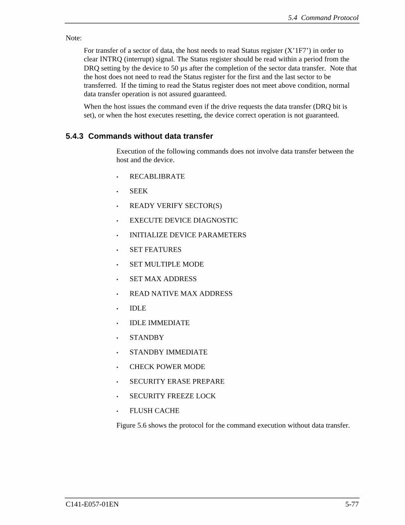
5.4 Command Protocol
C141-E057-01EN 5-77
Note:
For transfer of a sector of data, the host needs to read Status register (X’1F7’) in order toclear INTRQ (interrupt) signal. The Status register should be read within a period from theDRQ setting by the device to 50 µs after the completion of the sector data transfer. Note thatthe host does not need to read the Status register for the first and the last sector to betransferred. If the timing to read the Status register does not meet above condition, normaldata transfer operation is not assured guaranteed.
When the host issues the command even if the drive requests the data transfer (DRQ bit isset), or when the host executes resetting, the device correct operation is not guaranteed.
5.4.3 Commands without data transfer
Execution of the following commands does not involve data transfer between thehost and the device.
• RECABLIBRATE
• SEEK
• READY VERIFY SECTOR(S)
• EXECUTE DEVICE DIAGNOSTIC
• INITIALIZE DEVICE PARAMETERS
• SET FEATURES
• SET MULTIPLE MODE
• SET MAX ADDRESS
• READ NATIVE MAX ADDRESS
• IDLE
• IDLE IMMEDIATE
• STANDBY
• STANDBY IMMEDIATE
• CHECK POWER MODE
• SECURITY ERASE PREPARE
• SECURITY FREEZE LOCK
• FLUSH CACHE
Figure 5.6 shows the protocol for the command execution without data transfer.
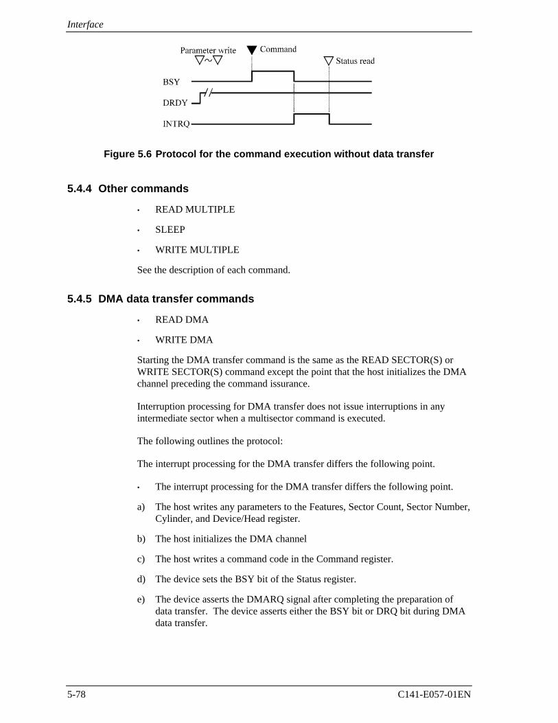
Interface
5-78 C141-E057-01EN
Figure 5.6 Protocol for the command execution without data transfer
5.4.4 Other commands
• READ MULTIPLE
• SLEEP
• WRITE MULTIPLE
See the description of each command.
5.4.5 DMA data transfer commands
• READ DMA
• WRITE DMA
Starting the DMA transfer command is the same as the READ SECTOR(S) orWRITE SECTOR(S) command except the point that the host initializes the DMAchannel preceding the command issurance.
Interruption processing for DMA transfer does not issue interruptions in anyintermediate sector when a multisector command is executed.
The following outlines the protocol:
The interrupt processing for the DMA transfer differs the following point.
• The interrupt processing for the DMA transfer differs the following point.
a) The host writes any parameters to the Features, Sector Count, Sector Number,Cylinder, and Device/Head register.
b) The host initializes the DMA channel
c) The host writes a command code in the Command register.
d) The device sets the BSY bit of the Status register.
e) The device asserts the DMARQ signal after completing the preparation ofdata transfer. The device asserts either the BSY bit or DRQ bit during DMAdata transfer.
5.4 Command Protocol
C141-E057-01EN 5-79
f) When the command execution is completed, the device clears both BSY andDRQ bits and asserts the INTRQ signal. Then, the host reads the Statusregister.
g) The host resets the DMA channel.
Figure 5.7 shows the correct DMA data transfer protocol.
Figure 5.7 Normal DMA data transfer
fd
e
e
d
g
d
f
f
Interface
5-80 C141-E057-01EN
5.5 Ultra DMA Feature Set
5.5.1 Overview
Ultra DMA is a data transfer protocol used with the READ DMA and WRITEDMA commands. When this protocol is enabled it shall be used instead of theMultiword DMA protocol when these commands are issued by the host. Thisprotocol applies to the Ultra DMA data burst only. When this protocol is usedthere are no changes to other elements of the ATA protocol (e.g.: CommandBlock Register access).
Several signal lines are redefined to provide new functions during an Ultra DMAburst. These lines assume these definitions when 1) an Ultra DMA Mode isselected, and 2) a host issues a READ DMA or a WRITE DMA, commandrequiring data transfer, and 3) the host asserts DMACK-. These signal lines revertback to the definitions used for non-Ultra DMA transfers upon the negation ofDMACK- by the host at the termination of an Ultra DMA burst. All of thecontrol signals are unidirectional. DMARQ and DMACK- retain their standarddefinitions.
With the Ultra DMA protocol, the control signal (STROBE) that latches data fromDD (15:0) is generated by the same agent (either host or device) that drives thedata onto the bus. Ownership of DD (15:0) and this data strobe signal are giveneither to the device during an Ultra DMA data in burst or to the host for an UltraDMA data out burst.
During an Ultra DMA burst a sender shall always drive data onto the bus, andafter a sufficient time to allow for propagation delay, cable settling, and setuptime, the sender shall generate a STROBE edge to latch the data. Both edges ofSTROBE are used for data transfers so that the frequency of STROBE is limitedto the same frequency as the data. The highest fundamental frequency on thecable shall be 16.67 million transitions per second or 8.33 MHz (the same as themaximum frequency for PIO Mode 4 and DMA Mode 2).
Words in the IDENTIFY DEVICE data indicate support of the Ultra DMA featureand the Ultra DMA Modes the device is capable of supporting. The Set transfermode subcommand in the SET FEATURES command shall be used by a host toselect the Ultra DMA Mode at which the system operates. The Ultra DMA Modeselected by a host shall be less than or equal to the fastest mode of which thedevice is capable. Only the Ultra DMA Mode shall be selected at any given time.All timing requirements for a selected Ultra DMA Mode shall be satisfied.Devices supporting Ultra DMA Mode 2 shall also support Ultra DMA Modes 0and 1. Devices supporting Ultra DMA Mode 1 shall also support Ultra DMAMode 0.
An Ultra DMA capable device shall retain its previously selected Ultra DMAMode after executing a Software reset sequence. An Ultra DMA capable deviceshall clear any previously selected Ultra DMA Mode and revert to its default non-Ultra DMA Modes after executing a Power on or hardware reset.
5.5 Ultra DMA Feature Set
C141-E057-01EN 5-81
Both the host and device perform a CRC function during an Ultra DMA burst. Atthe end of an Ultra DMA burst the host sends the its CRC data to the device. Thedevice compares its CRC data to the data sent from the host. If the two values donot match the device reports an error in the error register at the end of thecommand. If an error occurs during one or more Ultra DMA bursts for any onecommand, at the end of the command, the device shall report the first error thatoccurred.
5.5.2 Phases of operation
An Ultra DMA data transfer is accomplished through a series of Ultra DMA datain or data out bursts. Each Ultra DMA burst has three mandatory phases ofoperation: the initiation phase, the data transfer phase, and the Ultra DMA bursttermination phase. In addition, an Ultra DMA burst may be paused during thedata transfer phase (see 5.5.3 and 5.5.4 for the detailed protocol descriptions foreach of these phases, 5.6.4 defines the specific timing requirements). In thefollowing rules DMARDY- is used in cases that could apply to eitherDDMARDY- or HDMARDY-, and STROBE is used in cases that could apply toeither DSTROBE or HSTROBE. The following are general Ultra DMA rules.
a) An Ultra DMA burst is defined as the period from an assertion of DMACK-by the host to the subsequent negation of DMACK-.
b) A recipient shall be prepared to receive at least two data words whenever itenters or resumes an Ultra DMA burst.
5.5.2.1 Ultra DMA burst initiation phase
a) The Ultra DMA burst initiation phase is started by the assertion of DMARQsignal by the device, and is ended when the transmitting side has invertedSTROBE signal for transmitting the first data.
b) The Ultra DMA burst requires the assertion of DMARQ signal by the device.
c) The host asserts DMACK-signal when it is able to start the requested burst.
d) The host always asserts DMACK signal after detecting the first assertion ofDMARQ signal.
e) Ultra DMA data in burst
The device starts transmission of the data to DD (15 : 0) when;
• DMACK-signal assertion has been detected,
• STOP signal negation has been detected, or
• HDMARDY-signal assertion has been detected.
f) Ultra DMA data out burst
The device should not invert the state of this signal in the period from themoment of DMARQ signal assertion or DDMARDY-signal assertion to themoment of inversion of the first STROBE signal.
Interface
5-82 C141-E057-01EN
g) Ultra DMA data in burst
The device should not invert the state of this signal in the period from themoment of STOP signal negation or HDMARDY-signal assertion to themoment of inversion of the first STROBE signal.
5.5.2.2 Data transfer phase
a) The Data transfer phase is defined as the period from The Ultra DMA burstinitiation phase to Ultra DMA burst termination phase.
b) The receiving side stops the Ultra DMA burst temporarily by negatingDMARDY-signal, and then restarts the Ultra DMA burst by asserting again.
c) The transmitting side stops the Ultra DMA burst temporarily by not-performing inversion of STROBE signal, and then restarts the Ultra DMAburst by restarting the inversion.
d) When the transmitting side has stopped the inversion of STROBE signal, thereceiving side should not output termination request signal immediately.
The receiving side should negate DMARDY signal when no terminationrequest signal has been received from the transmission side, and then shouldoutput the termination request signal when a certain wait time has elapsed.
e) The transmitting side is allowed to send STROBE signal at a transfer speedthat is lower than the one in the transferable fastest Ultra DMA mode, but isnot allowed to send the STROBE signal at a higher speed than this.
The receiving side should be able to receive the data in the transferable fastestUltra DMA mode.
5.5.2.3 Ultra DMA burst termination phase
a) The transmitting side or receiving side is allowed to end the Ultra DMAburst.
b) The Ultra DMA burst termination is not the end of the command execution.When the Ultra DMA burst termination has occurred before the ending of thecommand, the command should be ended by starting a new Ultra DMA burst,or the host should issue command abort by outputting hard reset or soft resetto the device.
c) The Ultra DMA burst should be stopped temporarily before the receiving sideoutputs the ending request.
d) The host outputs the ending request by asserting STOP signal, and then thedevice negates DMARQ signal to confirm it.
e) The device outputs the ending request by negating DMARQ signal, and thenthe host asserts STOP signal to confirm it.
5.5 Ultra DMA Feature Set
C141-E057-01EN 5-83
f) Once the transmitting side has outputted the ending request, the output stateof STROBE signal should not be changed unless the receiving side hasconfirmed it. Then, if the STROBE signal is not in asserted state, Thetransmitting side should assert the STROBE signal. However, the assertion ofthe STROBE signal should not cause the data transfer to occur.
g) The transmitting side should return the STROBE signal to its asserted stateimmediately after receiving the ending request from the receiving side.
However, the returning of the STROBE signal to its asserted state should notcause the data transfer to occur and CRC to be perform.
h) Once the receiving side has outputted the ending request, the negated state ofthe DMARDY signal should not be changed for the remaining Ultra DMAburst to be performed.
i) The receiving side should neglect the inversion of the STROBE signal ifDMARQ signal has been negated or STOP signal has been asserted.
5.5.3 Ultra DMA data in commands
5.5.3.1 Initiating an Ultra DMA data in burst
The following steps shall occur in the order they are listed unless otherwisespecifically allowed (see 5.6.4.1 and 5.6.4.2 for specific timing requirements):
1) The host shall keep DMACK- in the negated state before an Ultra DMA burstis initiated.
2) The device shall assert DMARQ to initiate an Ultra DMA burst. Afterassertion of DMARQ the device shall not negate DMARQ until after the firstnegation of DSTROBE.
3) Steps (3), (4) and (5) may occur in any order or at the same time. The hostshall assert STOP.
4) The host shall negate HDMARDY-.
5) The host shall negate CS0-, CS1-, DA2, DA1, and DA0. The host shall keepCS0-, CS1-, DA2, DA1, and DA0 negated until after negating DMACK- atthe end of the burst.
6) Steps (3), (4) and (5) shall have occurred at least tACK
before the host assertsDMACK-. The host shall keep DMACK- asserted until the end of an UltraDMA burst.
7) The host shall release DD (15:0) within tAZ
after asserting DMACK-.
8) The device may assert DSTROBE tZIORDY
after the host has asserted DMACK-.Once the device has driven DSTROBE the device shall not releaseDSTROBE until after the host has negated DMACK- at the end of an UltraDMA burst.
Interface
5-84 C141-E057-01EN
9) The host shall negate STOP and assert HDMARDY- within tENV
afterasserting DMACK-. After negating STOP and asserting HDMARDY-, thehost shall not change the state of either signal until after receiving the firsttransition of DSTROBE from the device (i.e., after the first data word hasbeen received).
10) The device shall drive DD (15:0) no sooner than tZAD
after the host hasasserted DMACK-, negated STOP, and asserted HDMARDY-.
11) The device shall drive the first word of the data transfer onto DD (15:0). Thisstep may occur when the device first drives DD (15:0) in step (10).
12) To transfer the first word of data the device shall negate DSTROBE within tFS
after the host has negated STOP and asserted HDMARDY-. The device shallnegate DSTROBE no sooner than t
DVS after driving the first word of data onto
DD (15:0).
5.5.3.2 The data in transfer
The following steps shall occur in the order they are listed unless otherwisespecifically allowed (see 5.6.4.3 and 5.6.4.2):
1) The device shall drive a data word onto DD (15:0).
2) The device shall generate a DSTROBE edge to latch the new word no soonerthan t
DVS after changing the state of DD (15:0). The device shall generate a
DSTROBE edge no more frequently than tCYC
for the selected Ultra DMAMode. The device shall not generate two rising or two falling DSTROBEedges more frequently than 2t
CYC for the selected Ultra DMA mode.
3) The device shall not change the state of DD (15:0) until at least tDVH
aftergenerating a DSTROBE edge to latch the data.
4) The device shall repeat steps (1), (2) and (3) until the data transfer is completeor an Ultra DMA burst is paused, whichever occurs first.
5.5.3.3 Pausing an Ultra DMA data in burst
The following steps shall occur in the order they are listed unless otherwisespecifically allowed (see 5.6.4.4 and 5.6.4.2 for specific timing requirements).
a) Device pausing an Ultra DMA data in burst
1) The device shall not pause an Ultra DMA burst until at least one dataword of an Ultra DMA burst has been transferred.
2) The device shall pause an Ultra DMA burst by not generating DSTROBEedges.
NOTE - The host shall not immediately assert STOP to initiate UltraDMA burst termination when the device stops generating STROBEedges. If the device does not negate DMARQ, in order to initiateULTRA DMA burst termination, the host shall negate HDMARDY- andwait t
RP before asserting STOP.
5.5 Ultra DMA Feature Set
C141-E057-01EN 5-85
3) The device shall resume an Ultra DMA burst by generating a DSTROBEedge.
b) Host pausing an Ultra DMA data in burst
1) The host shall not pause an Ultra DMA burst until at least one data wordof an Ultra DMA burst has been transferred.
2) The host shall pause an Ultra DMA burst by negating HDMARDY-.
3) The device shall stop generating DSTROBE edges within tRFS
of the hostnegating HDMARDY-.
4) If the host negates HDMARDY- within tSR
after the device has generateda DSTROBE edge, then the host shall be prepared to receive zero or oneadditional data words. If the host negates HDMARDY- greater than t
SR
after the device has generated a DSTROBE edge, then the host shall beprepared to receive zero, one or two additional data words. Theadditional data words are a result of cable round trip delay and t
RFS timing
for the device.
5) The host shall resume an Ultra DMA burst by asserting HDMARDY-.
5.5.3.4 Terminating an Ultra DMA data in burst
a) Device terminating an Ultra DMA data in burst
The following steps shall occur in the order they are listed unless otherwisespecifically allowed (see 5.6.4.5 and 5.6.4.2 for specific timingrequirements):
1) The device shall initiate termination of an Ultra DMA burst by notgenerating DSTROBE edges.
2) The device shall negate DMARQ no sooner than tSS
after generating thelast DSTROBE edge. The device shall not assert DMARQ again untilafter the Ultra DMA burst is terminated.
3) The device shall release DD (15:0) no later than tAZ
after negatingDMARQ.
4) The host shall assert STOP within tLI after the device has negated
DMARQ. The host shall not negate STOP again until after the UltraDMA burst is terminated.
5) The host shall negate HDMARDY- within tLI after the device has negated
DMARQ. The host shall continue to negate HDMARDY- until the UltraDMA burst is terminated. Steps (4) and (5) may occur at the same time.
6) The host shall drive DD (15:0) no sooner than tZAH
after the device hasnegated DMARQ. For this step, the host may first drive DD (15:0) withthe result of its CRC calculation (see 5.5.5):
Interface
5-86 C141-E057-01EN
7) If DSTROBE is negated, the device shall assert DSTROBE within tLI
after the host has asserted STOP. No data shall be transferred during thisassertion. The host shall ignore this transition on DSTROBE.DSTROBE shall remain asserted until the Ultra DMA burst isterminated.
8) If the host has not placed the result of its CRC calculation on DD (15:0)since first driving DD (15:0) during (6), the host shall place the result ofits CRC calculation on DD (15:0) (see 5.5.5).
9) The host shall negate DMACK- no sooner than tMLI
after the device hasasserted DSTROBE and negated DMARQ and the host has assertedSTOP and negated HDMARDY-, and no sooner than t
DVS after the host
places the result of its CRC calculation on DD (15:0).
10) The device shall latch the host's CRC data from DD (15:0) on thenegating edge of DMACK-.
11) The device shall compare the CRC data received from the host with theresults of its own CRC calculation. If a miscompare error occurs duringone or more Ultra DMA bursts for any one command, at the end of thecommand the device shall report the first error that occurred (see 5.5.5).
12) The device shall release DSTROBE within tIORDYZ
after the host negatesDMACK-.
13) The host shall not negate STOP no assert HDMARDY- until at least tACK
after negating DMACK-.
14) The host shall not assert DIOR-, CS0-, CS1-, DA2, DA1, or DA0 until atleast t
ACK after negating DMACK.
b) Host terminating an Ultra DMA data in burst
The following steps shall occur in the order they are listed unless otherwisespecifically allowed (see 5.6.4.6 and 5.6.4.2 for specific timingrequirements):
1) The host shall not initiate Ultra DMA burst termination until at least onedata word of an Ultra DMA burst has been transferred.
2) The host shall initiate Ultra DMA burst termination by negatingHDMARDY-. The host shall continue to negate HDMARDY- until theUltra DMA burst is terminated.
3) The device shall stop generating DSTROBE edges within tRFS
of the hostnegating HDMARDY-.
4) If the host negates HDMARDY- within tSR
after the device has generateda DSTROBE edge, then the host shall be prepared to receive zero or oneadditional data words. If the host negates HDMARDY- greater than t
SR
after the device has generated a DSTROBE edge, then the host shall beprepared to receive zero, one or two additional data words. Theadditional data words are a result of cable round trip delay and t
RFS timing
for the device.
5.5 Ultra DMA Feature Set
C141-E057-01EN 5-87
5) The host shall assert STOP no sooner than tRP
after negatingHDMARDY-. The host shall not negate STOP again until after the UltraDMA burst is terminated.
6) The device shall negate DMARQ within tLI after the host has asserted
STOP. The device shall not assert DMARQ again until after the UltraDMA burst is terminated.
7) If DSTROBE is negated, the device shall assert DSTROBE within tLI
after the host has asserted STOP. No data shall be transferred during thisassertion. The host shall ignore this transition on DSTROBE.DSTROBE shall remain asserted until the Ultra DMA burst isterminated.
8) The device shall release DD (15:0) no later than tAZ
after negatingDMARQ.
9) The host shall drive DD (15:0) no sooner than tZAH
after the device hasnegated DMARQ. For this step, the host may first drive DD (15:0) withthe result of its CRC calculation (see 5.5.5).
10) If the host has not placed the result of its CRC calculation on DD (15:0)since first driving DD (15:0) during (9), the host shall place the result ofits CRC calculation on DD (15:0) (see 5.5.5).
11) The host shall negate DMACK- no sooner than tMLI
after the device hasasserted DSTROBE and negated DMARQ and the host has assertedSTOP and negated HDMARDY-, and no sooner than t
DVS after the host
places the result of its CRC calculation on DD (15:0).
12) The device shall latch the host's CRC data from DD (15:0) on thenegating edge of DMACK-.
13) The device shall compare the CRC data received from the host with theresults of its own CRC calculation. If a miscompare error occurs duringone or more Ultra DMA burst for any one command, at the end of thecommand, the device shall report the first error that occurred (see 5.5.5).
14) The device shall release DSTROBE within tIORDYZ
after the host negatesDMACK-.
15) The host shall neither negate STOP nor assert HDMARDY- until at leastt
ACK after the host has negated DMACK-.
16) The host shall not assert DIOR-, CS0-, CS1-, DA2, DA1, or DA0 until atleast t
ACK after negating DMACK.
Interface
5-88 C141-E057-01EN
5.5.4 Ultra DMA data out commands
5.5.4.1 Initiating an Ultra DMA data out burst
The following steps shall occur in the order they are listed unless otherwisespecifically allowed (see 5.6.4.7 and 5.6.4.2 for specific timing requirements):
1) The host shall keep DMACK- in the negated state before an Ultra DMA burstis initiated.
2) The device shall assert DMARQ to initiate an Ultra DMA burst.
3) Steps (3), (4), and (5) may occur in any order or at the same time. The hostshall assert STOP.
4) The host shall assert HSTROBE.
5) The host shall negate CS0-, CS1-, DA2, DA1, and DA0. The host shall keepCS0-, CS1-, DA2, DA1, and DA0 negated until after negating DMACK- atthe end of the burst.
6) Steps (3), (4), and (5) shall have occurred at least tACK
before the host assertsDMACK-. The host shall keep DMACK- asserted until the end of an UltraDMA burst.
7) The device may negate DDMARDY- tZIORDY
after the host has assertedDMACK-. Once the device has negated DDMARDY-, the device shall notrelease DDMARDY- until after the host has negated DMACK- at the end ofan Ultra DMA burst.
8) The host shall negate STOP within tENV
after asserting DMACK-. The hostshall not assert STOP until after the first negation of HSTROBE.
9) The device shall assert DDMARDY- within tLI after the host has negated
STOP. After asserting DMARQ and DDMARDY- the device shall notnegate either signal until after the first negation of HSTROBE by the host.
10) The host shall drive the first word of the data transfer onto DD (15:0). Thisstep may occur any time during Ultra DMA burst initiation.
11) To transfer the first word of data: the host shall negate HSTROBE no soonerthan t
LI after the device has asserted DDMARDY-. The host shall negate
HSTROBE no sooner than tDVS
after the driving the first word of data ontoDD (15:0).
5.5.4.2 The data out transfer
The following steps shall occur in the order they are listed unless otherwisespecifically allowed (see 5.6.4.8 and 5.6.4.2 for specific timing requirements):
1) The host shall drive a data word onto DD (15:0).
2) The host shall generate an HSTROBE edge to latch the new word no soonerthan t
DVS after changing the state of DD (15:0). The host shall generate an
5.5 Ultra DMA Feature Set
C141-E057-01EN 5-89
HSTROBE edge no more frequently than tCYC
for the selected Ultra DMAMode. The host shall not generate two rising or falling HSTROBE edgesmore frequently than 2 t
CYC for the selected Ultra DMA mode.
3) The host shall not change the state of DD (15:0) until at least tDVH
aftergenerating an HSTROBE edge to latch the data.
4) The host shall repeat steps (1), (2) and (3) until the data transfer is completeor an Ultra DMA burst is paused, whichever occurs first.
5.5.4.3 Pausing an Ultra DMA data out burst
The following steps shall occur in the order they are listed unless otherwisespecifically allowed (see 5.6.4.9 and 5.6.4.2 for specific timing requirements).
a) Host pausing an Ultra DMA data out burst
1) The host shall not pause an Ultra DMA burst until at least one data wordof an Ultra DMA burst has been transferred.
2) The host shall pause an Ultra DMA burst by not generating anHSTROBE edge.
Note: The device shall not immediately negate DMARQ to initiate UltraDMA burst termination when the host stops generating HSTROBEedges. If the host does not assert STOP, in order to initiate Ultra DMAburst termination, the device shall negate DDMARDY- and wait t
RP
before negating DMARQ.
3) The host shall resume an Ultra DMA burst by generating an HSTROBEedge.
b) Device pausing an Ultra DMA data out burst
1) The device shall not pause an Ultra DMA burst until at least one dataword of an Ultra DMA burst has been transferred.
2) The device shall pause an Ultra DMA burst by negating DDMARDY-.
3) The host shall stop generating HSTROBE edges within tRFS
of the devicenegating DDMARDY-.
4) If the device negates DDMARDY- within tSR
after the host has generatedan HSTROBE edge, then the device shall be prepared to receive zero orone additional data words. If the device negates DDMARDY- greaterthan t
SR after the host has generated an HSTROBE edge, then the device
shall be prepared to receive zero, one or two additional data words. Theadditional data words are a result of cable round trip delay and t
RFS timing
for the host.
5) The device shall resume an Ultra DMA burst by asserting DDMARDY-.
Interface
5-90 C141-E057-01EN
5.5.4.4 Terminating an Ultra DMA data out burst
a) Host terminating an Ultra DMA data out burst
The following stops shall occur in the order they are listed unless otherwisespecifically allowed (see 5.6.4.10 and 5.6.4.2 for specific timingrequirements):
1) The host shall initiate termination of an Ultra DMA burst by notgenerating HSTROBE edges.
2) The host shall assert STOP no sooner than tSS
after it last generated anHSTROBE edge. The host shall not negate STOP again until after theUltra DMA burst is terminated.
3) The device shall negate DMARQ within tLI after the host asserts STOP.
The device shall not assert DMARQ again until after the Ultra DMAburst is terminated.
4) The device shall negate DDMARDY- with tLI after the host has negated
STOP. The device shall not assert DDMARDY- again until after theUltra DMA burst termination is complete.
5) If HSTROBE is negated, the host shall assert HSTROBE with tLI after
the device has negated DMARQ. No data shall be transferred during thisassertion. The device shall ignore this transition on HSTROBE.HSTROBE shall remain asserted until the Ultra DMA burst isterminated.
6) The host shall place the result of its CRC calculation on DD (15:0) (see5.5.5)
7) The host shall negate DMACK- no sooner than tMLI
after the host hasasserted HSTROBE and STOP and the device has negated DMARQ andDDMARDY-, and no sooner than t
DVS after placing the result of its CRC
calculation on DD (15:0).
8) The device shall latch the host's CRC data from DD (15:0) on thenegating edge of DMACK-.
9) The device shall compare the CRC data received from the host with theresults of its own CRC calculation. If a miscompare error occurs duringone or more Ultra DMA bursts for any one command, at the end of thecommand, the device shall report the first error that occurred (see 5.5.5).
10) The device shall release DDMARDY- within tIORDYZ
after the host hasnegated DMACK-.
11) The host shall neither negate STOP nor negate HSTROBE until at leastt
ACK after negating DMACK-.
12) The host shall not assert DIOW-, CS0-, CS1-, DA2, DA1, or DA0 untilat least t
ACK after negating DMACK.
5.5 Ultra DMA Feature Set
C141-E057-01EN 5-91
b) Device terminating an Ultra DMA data out burst
The following steps shall occur in the order they are listed unless otherwisespecifically allowed (see 5.6.4.11 and 5.6.4.2 for specific timingrequirements):
1) The device shall not initiate Ultra DMA burst termination until at leastone data word of an Ultra DMA burst has been transferred.
2) The device shall initiate Ultra DMA burst termination by negatingDDMARDY-.
3) The host shall stop generating an HSTROBE edges within tRFS
of thedevice negating DDMARDY-.
4) If the device negates DDMARDY- within tSR
after the host has generatedan HSTROBE edge, then the device shall be prepared to receive zero orone additional data words. If the device negates DDMARDY- greaterthan t
SR after the host has generated an HSTROBE edge, then the device
shall be prepared to receive zero, one or two additional data words. Theadditional data words are a result of cable round trip delay and t
RFS timing
for the host.
5) The device shall negate DMARQ no sooner than tRP
after negatingDDMARDY-. The device shall not assert DMARQ again until after theUltra DMA burst is terminated.
6) The host shall assert STOP with tLI after the device has negated DMARQ.
The host shall not negate STOP again until after the Ultra DMA burst isterminated.
7) If HSTROBE is negated, the host shall assert HSTROBE with tLI after
the device has negated DMARQ. No data shall be transferred during thisassertion. The device shall ignore this transition of HSTROBE.HSTROBE shall remain asserted until the Ultra DMA burst isterminated.
8) The host shall place the result of its CRC calculation on DD (15:0) (see5.5.5).
9) The host shall negate DMACK- no sooner than tMLI
after the host hasasserted HSTROBE and STOP and the device has negated DMARQ andDDMARDY-, and no sooner than t
DVS after placing the result of its CRC
calculation on DD (15:0).
10) The device shall latch the host's CRC data from DD (15:0) on thenegating edge of DMACK-.
11) The device shall compare the CRC data received from the host with theresults of its own CRC calculation. If a miscompare error occurs duringone or more Ultra DMA bursts for any one command, at the end of thecommand, the device shall report the first error that occurred (see 5.5.5).
12) The device shall release DDMARDY- within tIORDYZ
after the host has negatedDMACK-.
Interface
5-92 C141-E057-01EN
13) The host shall neither negate STOP nor HSTROBE until at least tACK
afternegating DMACK-.
14) The host shall not assert DIOW-, CS0-, CS1-, DA2, DA1, or DA0 untilat least t
ACK after negating DMACK.
5.5.5 Ultra DMA CRC rules
The following is a list of rules for calculating CRC, determining if a CRC errorhas occurred during an Ultra DMA burst, and reporting any error that occurs at theend of a command.
a) Both the host and the device shall have a 16-bit CRC calculation function.
b) Both the host and the device shall calculate a CRC value for each Ultra DMAburst.
c) The CRC function in the host and the device shall be initialized with a seedof 4ABAh at the beginning of an Ultra DMA burst before any data istransferred.
d) For each STROBE transition used for data transfer, both the host and thedevice shall calculate a new CRC value by applying the CRC polynomial tothe current value of their individual CRC functions and the word beingtransferred. CRC is not calculated for the return of STROBE to the assertedstate after the Ultra DMA burst termination request has been acknowledged.
e) At the end of any Ultra DMA burst the host shall send the results of its CRCcalculation function to the device on DD (15:0) with the negation ofDMACK-.
f) The device shall then compare the CRC data from the host with the calculatedvalue in its own CRC calculation function. If the two values do not match,the device shall save the error and report it at the end of the command. Asubsequent Ultra DMA burst for the same command that does not have aCRC error shall not clear an error saved from a previous Ultra DMa burst inthe same command. If a miscompare error occurs during one or more UltraDMA bursts for any one command, at the end of the command, the deviceshall report the first error that occurred.
g) For READ DMA or WRITE DMA commands: When a CRC error isdetected, it shall be reported by setting both ICRC and ABRT (bit 7 and bit 2in the Error register) to one. ICRC is defined as the "Interface CRC Error"bit. The host shall respond to this error by re-issuing the command.
h) A host may send extra data words on the last Ultra DMA burst of a data outcommand. If a device determines that all data has been transferred for acommand, the device shall terminate the burst. A device may have alreadyreceived more data words than were required for the command. These extrawords are used by both the host and the device to calculate the CRC, but, onan Ultra DMA data out burst, the extra words shall be discarded by thedevice.
i) The CRC generator polynomial is : G (X) = X16 + X12 + X5 + 1.
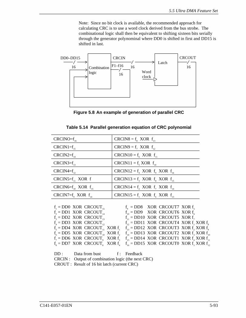
5.5 Ultra DMA Feature Set
C141-E057-01EN 5-93
Note: Since no bit clock is available, the recommended approach forcalculating CRC is to use a word clock derived from the bus strobe. Thecombinational logic shall then be equivalent to shifting sixteen bits seriallythrough the generator polynominal where DD0 is shifted in first and DD15 isshifted in last.
Figure 5.8 An example of generation of parallel CRC
Table 5.14 Parallel generation equation of CRC polynomial
CRCINO=f16
CRCIN8 = f8 XOR f
13
CRCIN1=f15
CRCIN9 = f7 XOR f
12
CRCIN2=f14
CRCIN10 = f6 XOR f
11
CRCIN3=f13
CRCIN11 = f5 XOR f
10
CRCIN4=f12
CRCIN12 = f4 XOR f
9 XOR f
16
CRCIN5=f11
XOR f CRCIN13 = f3 XOR f
8 XOR f
15
CRCIN6=f10
XOR f15
CRCIN14 = f2 XOR f
7 XOR f
14
CRCIN7=f9 XOR f
14CRCIN15 = f
1 XOR f
6 XOR f
13
f1 = DD0 XOR CRCOUT
15f
9 = DD8 XOR CRCOUT7 XOR f
5
f2 = DD1 XOR CRCOUT
14f
10 = DD9 XOR CRCOUT6 XOR f
6
f3 = DD2 XOR CRCOUT
13f
11 = DD10 XOR CRCOUT5 XOR f
7
f4 = DD3 XOR CRCOUT
12f
12 = DD11 XOR CRCOUT4 XOR f
1 XOR f
8
f5 = DD4 XOR CRCOUT
11 XOR f
1f
13 = DD12 XOR CRCOUT3 XOR f
2 XOR f
9
f6 = DD5 XOR CRCOUT
10 XOR f
2f
14 = DD13 XOR CRCOUT2 XOR f
3 XOR f
10
f7 = DD6 XOR CRCOUT
9 XOR f
3f
15 = DD14 XOR CRCOUT1 XOR f
4 XOR f
11
f8 = DD7 XOR CRCOUT
8 XOR f
4f
16 = DD15 XOR CRCOUT0 XOR f
5 XOR f
12
DD : Data from bust f : FeedbackCRCIN : Output of combination logic (the next CRC)CROUT : Result of 16 bit latch (current CRC)
Combinationlogic
CRCOUTLatch
16 16 16
16Wordclock
CRCINDD0–DD15
F1–f16
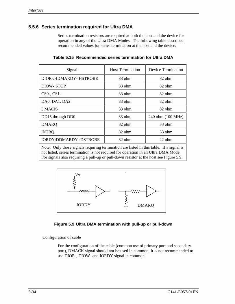
Interface
5-94 C141-E057-01EN
5.5.6 Series termination required for Ultra DMA
Series termination resistors are required at both the host and the device foroperation in any of the Ultra DMA Modes. The following table describesrecommended values for series termination at the host and the device.
Table 5.15 Recommended series termination for Ultra DMA
Signal Host Termination Device Termination
DIOR-:HDMARDY-:HSTROBE 33 ohm 82 ohm
DIOW-:STOP 33 ohm 82 ohm
CS0-, CS1- 33 ohm 82 ohm
DA0, DA1, DA2 33 ohm 82 ohm
DMACK- 33 ohm 82 ohm
DD15 through DD0 33 ohm 240 ohm (100 MHz)
DMARQ 82 ohm 33 ohm
INTRQ 82 ohm 33 ohm
IORDY:DDMARDY-:DSTROBE 82 ohm 22 ohm
Note: Only those signals requiring termination are listed in this table. If a signal isnot listed, series termination is not required for operation in an Ultra DMA Mode.For signals also requiring a pull-up or pull-down resistor at the host see Figure 5.9.
Figure 5.9 Ultra DMA termination with pull-up or pull-down
Configuration of cable
For the configuration of the cable (common use of primary port and secondaryport), DMACK signal should not be used in common. It is not recommended touse DIOR-, DIOW- and IORDY signal in common.
DMARQIORDY
5.6 Timing
C141-E057-01EN 5-95
5.6 Timing
5.6.1 PIO data transfer
Figure 5.10 shows of the data transfer timing between the device and the hostsystem.
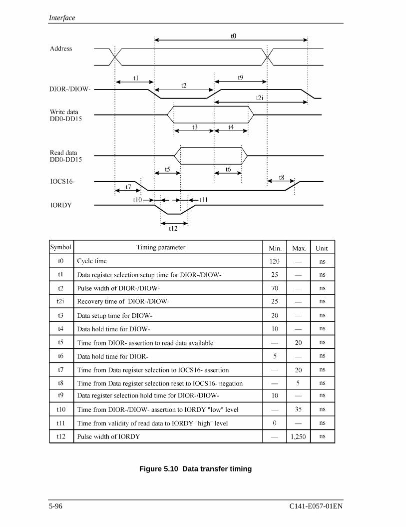
Interface
5-96 C141-E057-01EN
Figure 5.10 Data transfer timing
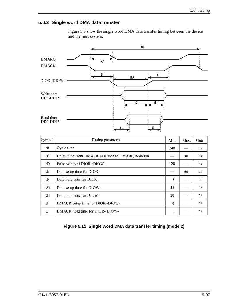
5.6 Timing
C141-E057-01EN 5-97
5.6.2 Single word DMA data transfer
Figure 5.9 show the single word DMA data transfer timing between the deviceand the host system.
Figure 5.11 Single word DMA data transfer timing (mode 2)
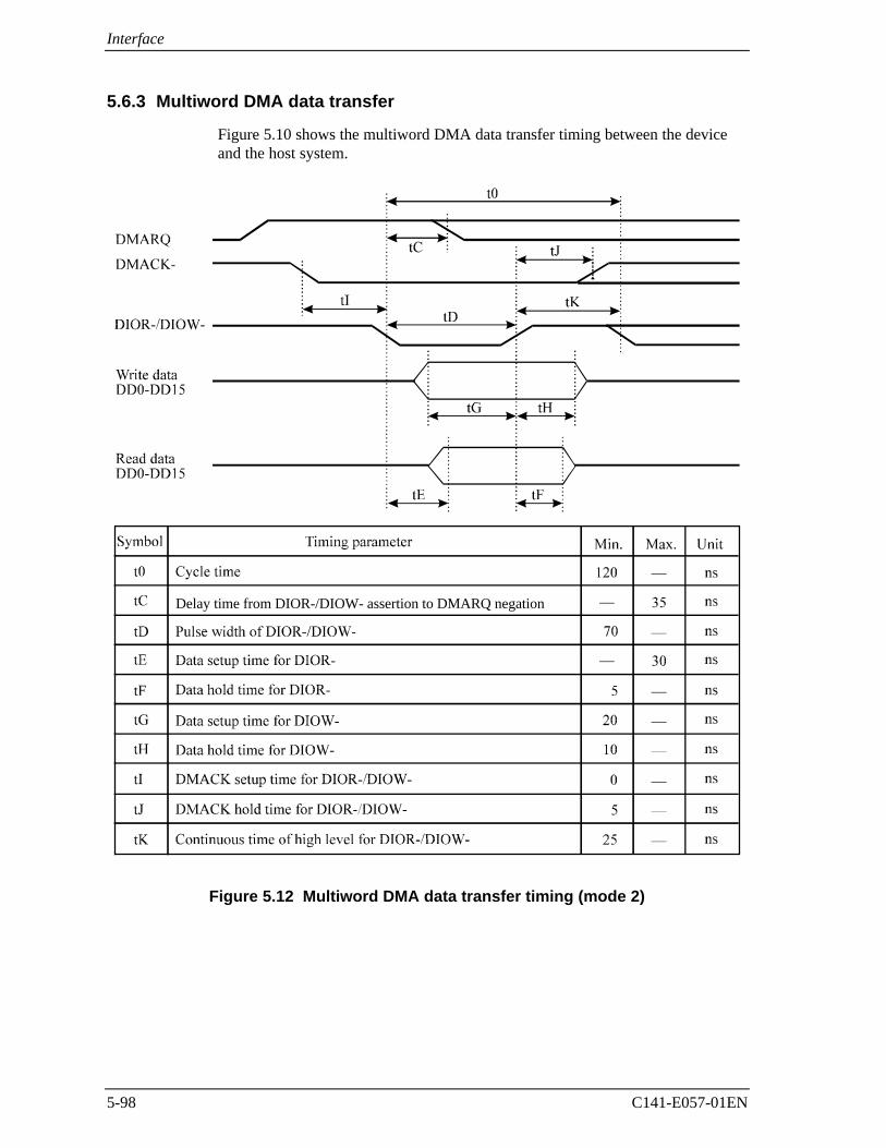
Interface
5-98 C141-E057-01EN
5.6.3 Multiword DMA data transfer
Figure 5.10 shows the multiword DMA data transfer timing between the deviceand the host system.
Delay time from DIOR-/DIOW- assertion to DMARQ negation
Figure 5.12 Multiword DMA data transfer timing (mode 2)
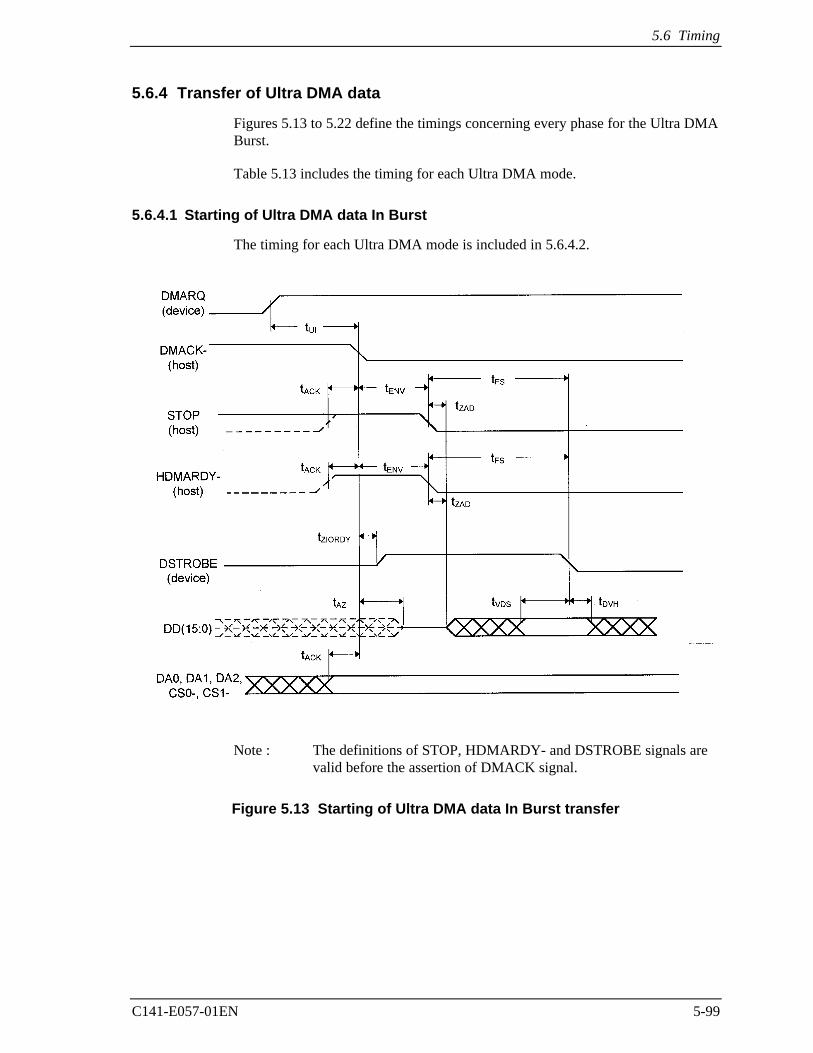
5.6 Timing
C141-E057-01EN 5-99
5.6.4 Transfer of Ultra DMA data
Figures 5.13 to 5.22 define the timings concerning every phase for the Ultra DMABurst.
Table 5.13 includes the timing for each Ultra DMA mode.
5.6.4.1 Starting of Ultra DMA data In Burst
The timing for each Ultra DMA mode is included in 5.6.4.2.
Note : The definitions of STOP, HDMARDY- and DSTROBE signals arevalid before the assertion of DMACK signal.
Figure 5.13 Starting of Ultra DMA data In Burst transfer
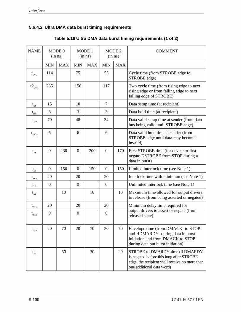
Interface
5-100 C141-E057-01EN
5.6.4.2 Ultra DMA data burst timing requirements
Table 5.16 Ultra DMA data burst timing requirements (1 of 2)
NAME MODE 0(in ns)
MODE 1(in ns)
MODE 2(in ns)
COMMENT
MIN MAX MIN MAX MIN MAX
tCYC
114 75 55 Cycle time (from STROBE edge toSTROBE edge)
t2CYC
235 156 117 Two cycle time (from rising edge to nextrising edge or from falling edge to nextfalling edge of STROBE)
tDS
15 10 7 Data setup time (at recipient)
tDH
3 3 3 Data hold time (at recipient)
tDVS
70 48 34 Data valid setup time at sender (from databus being valid until STROBE edge)
tDVH
6 6 6 Data valid hold time at sender (fromSTROBE edge until data may becomeinvalid)
tFS
0 230 0 200 0 170 First STROBE time (for device to firstnegate DSTROBE from STOP during adata in burst)
tLI
0 150 0 150 0 150 Limited interlock time (see Note 1)
tMLI
20 20 20 Interlock time with minimum (see Note 1)
tUI
0 0 0 Unlimited interlock time (see Note 1)
tAZ
10 10 10 Maximum time allowed for output driversto release (from being asserted or negated)
tZAH
20 20 20
tZAD
0 0 0
tENV
20 70 20 70 20 70 Envelope time (from DMACK- to STOPand HDMARDY- during data in burstinitiation and from DMACK to STOPduring data out burst initiation)
tSR
50 30 20 STROBE-to-DMARDY-time (if DMARDY-is negated before this long after STROBEedge, the recipient shall receive no more thanone additional data word)
Minimum delay time required foroutput drivers to assert or negate (fromreleased state)
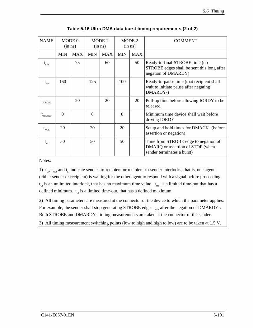
5.6 Timing
C141-E057-01EN 5-101
Table 5.16 Ultra DMA data burst timing requirements (2 of 2)
NAME MODE 0(in ns)
MODE 1(in ns)
MODE 2(in ns)
COMMENT
MIN MAX MIN MAX MIN MAX
tRFS
75 60 50 Ready-to-final-STROBE time (noSTROBE edges shall be sent this long afternegation of DMARDY)
tRP
160 125 100 Ready-to-pause time (that recipient shallwait to initiate pause after negatingDMARDY-)
tIORDYZ
20 20 20 Pull-up time before allowing IORDY to bereleased
tZIORDY
0 0 0 Minimum time device shall wait beforedriving IORDY
tACK
20 20 20 Setup and hold times for DMACK- (beforeassertion or negation)
tSS
50 50 50 Time from STROBE edge to negation ofDMARQ or assertion of STOP (whensender terminates a burst)
Notes:
1) tUI
, tMLI
and tLI indicate sender -to-recipient or recipient-to-sender interlocks, that is, one agent
(either sender or recipient) is waiting for the other agent to respond with a signal before proceeding.
tUI
is an unlimited interlock, that has no maximum time value. tMLI
is a limited time-out that has a
defined minimum. tLI is a limited time-out, that has a defined maximum.
2) All timing parameters are measured at the connector of the device to which the parameter applies.
For example, the sender shall stop generating STROBE edges tRFS
after the negation of DMARDY-.
Both STROBE and DMARDY- timing measurements are taken at the connector of the sender.
3) All timing measurement switching points (low to high and high to low) are to be taken at 1.5 V.
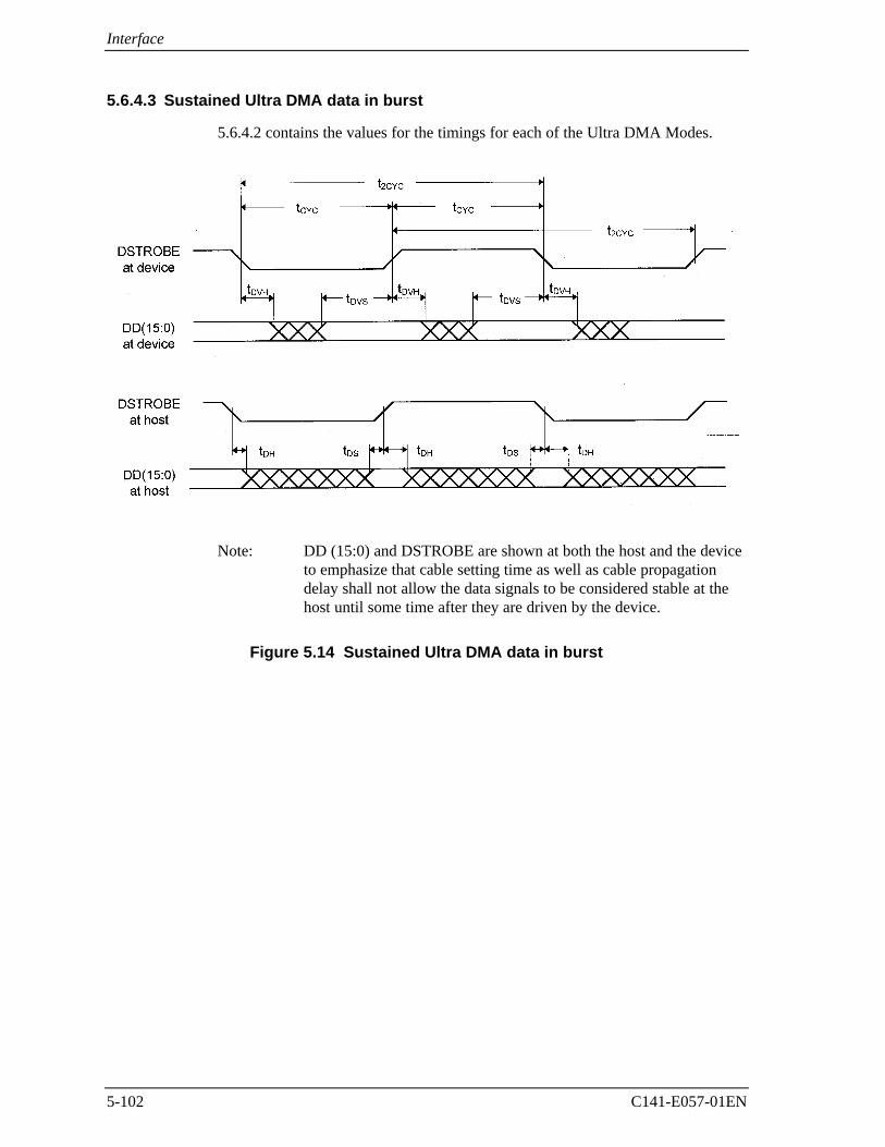
Interface
5-102 C141-E057-01EN
5.6.4.3 Sustained Ultra DMA data in burst
5.6.4.2 contains the values for the timings for each of the Ultra DMA Modes.
Note: DD (15:0) and DSTROBE are shown at both the host and the deviceto emphasize that cable setting time as well as cable propagationdelay shall not allow the data signals to be considered stable at thehost until some time after they are driven by the device.
Figure 5.14 Sustained Ultra DMA data in burst
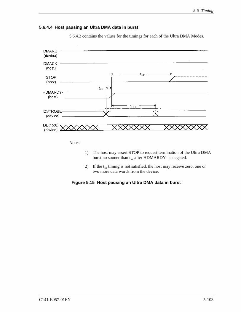
5.6 Timing
C141-E057-01EN 5-103
5.6.4.4 Host pausing an Ultra DMA data in burst
5.6.4.2 contains the values for the timings for each of the Ultra DMA Modes.
Notes:
1) The host may assert STOP to request termination of the Ultra DMAburst no sooner than t
RP after HDMARDY- is negated.
2) If the tSR
timing is not satisfied, the host may receive zero, one ortwo more data words from the device.
Figure 5.15 Host pausing an Ultra DMA data in burst
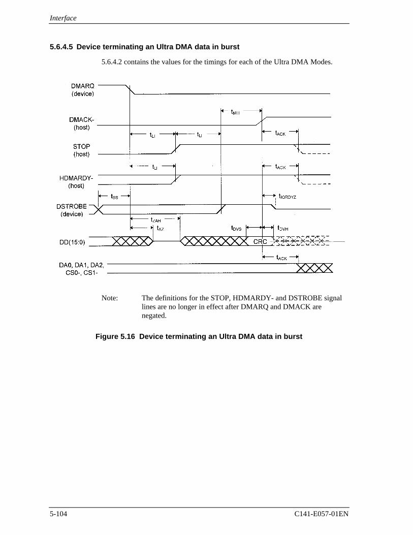
Interface
5-104 C141-E057-01EN
5.6.4.5 Device terminating an Ultra DMA data in burst
5.6.4.2 contains the values for the timings for each of the Ultra DMA Modes.
Note: The definitions for the STOP, HDMARDY- and DSTROBE signallines are no longer in effect after DMARQ and DMACK arenegated.
Figure 5.16 Device terminating an Ultra DMA data in burst
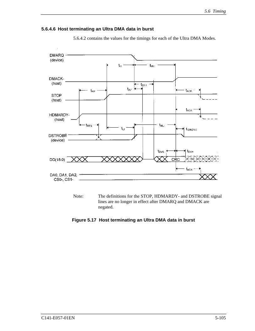
5.6 Timing
C141-E057-01EN 5-105
5.6.4.6 Host terminating an Ultra DMA data in burst
5.6.4.2 contains the values for the timings for each of the Ultra DMA Modes.
Note: The definitions for the STOP, HDMARDY- and DSTROBE signallines are no longer in effect after DMARQ and DMACK arenegated.
Figure 5.17 Host terminating an Ultra DMA data in burst
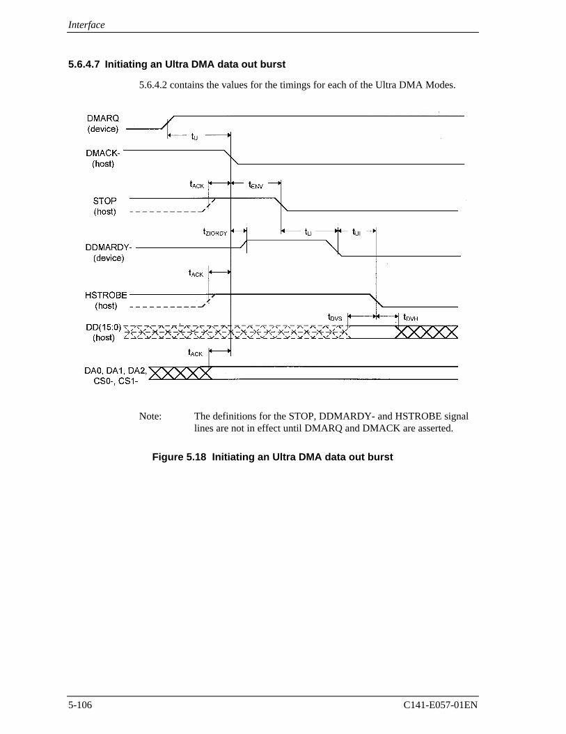
Interface
5-106 C141-E057-01EN
5.6.4.7 Initiating an Ultra DMA data out burst
5.6.4.2 contains the values for the timings for each of the Ultra DMA Modes.
Note: The definitions for the STOP, DDMARDY- and HSTROBE signallines are not in effect until DMARQ and DMACK are asserted.
Figure 5.18 Initiating an Ultra DMA data out burst
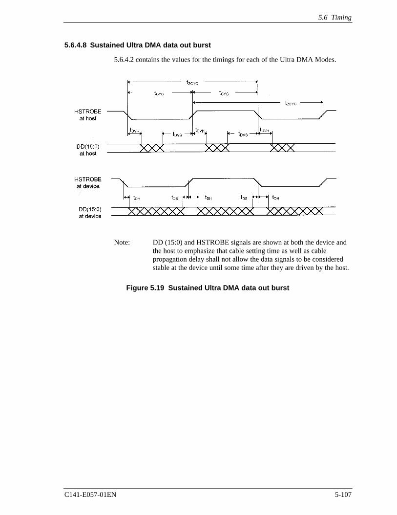
5.6 Timing
C141-E057-01EN 5-107
5.6.4.8 Sustained Ultra DMA data out burst
5.6.4.2 contains the values for the timings for each of the Ultra DMA Modes.
Note: DD (15:0) and HSTROBE signals are shown at both the device andthe host to emphasize that cable setting time as well as cablepropagation delay shall not allow the data signals to be consideredstable at the device until some time after they are driven by the host.
Figure 5.19 Sustained Ultra DMA data out burst
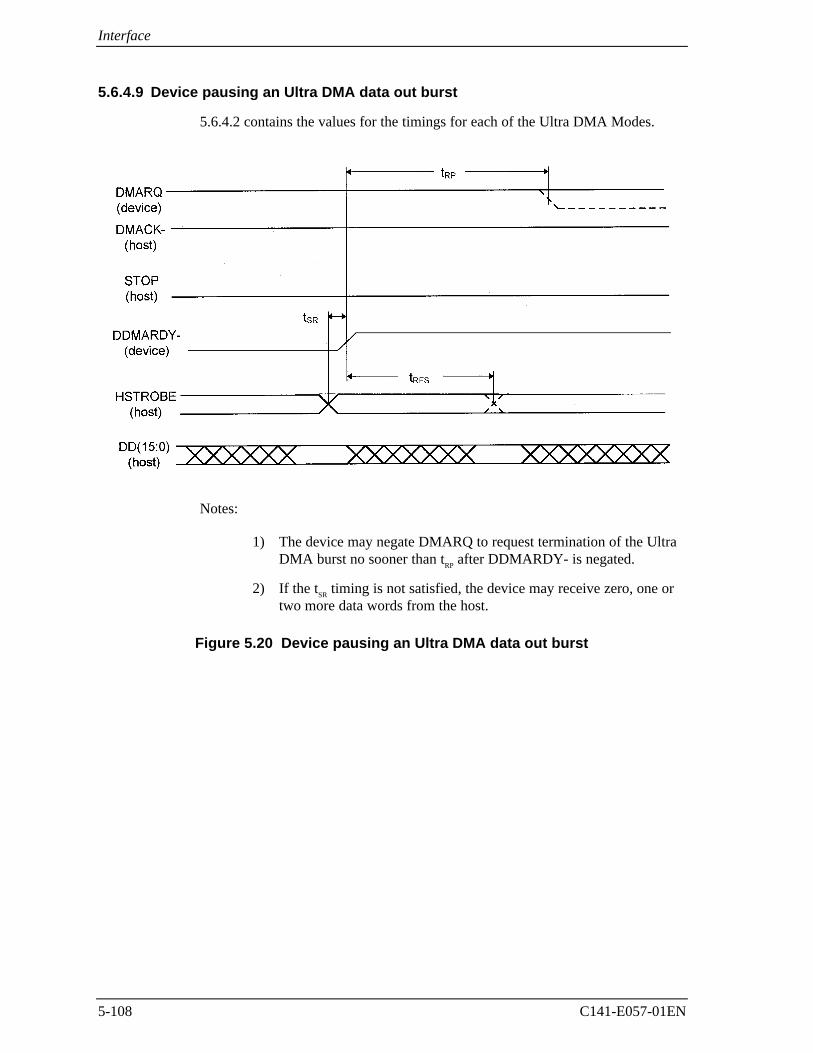
Interface
5-108 C141-E057-01EN
5.6.4.9 Device pausing an Ultra DMA data out burst
5.6.4.2 contains the values for the timings for each of the Ultra DMA Modes.
Notes:
1) The device may negate DMARQ to request termination of the UltraDMA burst no sooner than t
RP after DDMARDY- is negated.
2) If the tSR
timing is not satisfied, the device may receive zero, one ortwo more data words from the host.
Figure 5.20 Device pausing an Ultra DMA data out burst
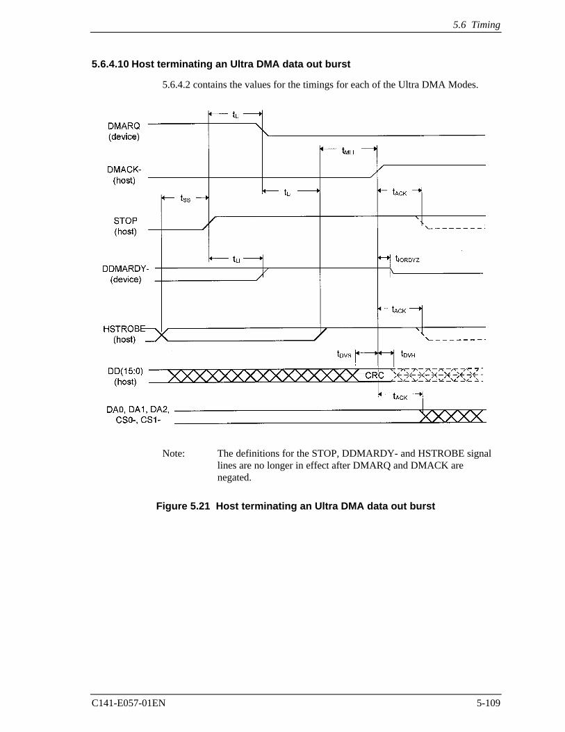
5.6 Timing
C141-E057-01EN 5-109
5.6.4.10 Host terminating an Ultra DMA data out burst
5.6.4.2 contains the values for the timings for each of the Ultra DMA Modes.
Note: The definitions for the STOP, DDMARDY- and HSTROBE signallines are no longer in effect after DMARQ and DMACK arenegated.
Figure 5.21 Host terminating an Ultra DMA data out burst
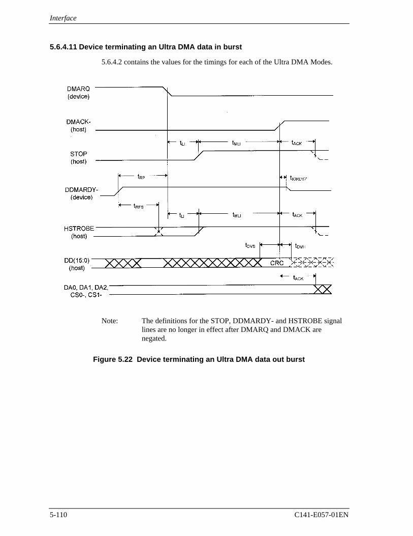
Interface
5-110 C141-E057-01EN
5.6.4.11 Device terminating an Ultra DMA data in burst
5.6.4.2 contains the values for the timings for each of the Ultra DMA Modes.
Note: The definitions for the STOP, DDMARDY- and HSTROBE signallines are no longer in effect after DMARQ and DMACK arenegated.
Figure 5.22 Device terminating an Ultra DMA data out burst
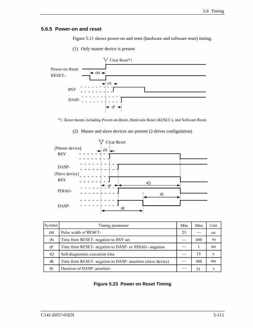
5.6 Timing
C141-E057-01EN 5-111
5.6.5 Power-on and reset
Figure 5.11 shows power-on and reset (hardware and software reset) timing.
(1) Only master device is present
(2) Master and slave devices are present (2-drives configulation)
Figure 5.23 Power on Reset Timing
31
Power-on ResetRESET–
PDIAG- negation

This page is intentionally left blank.
C141-E057-01EN 6-1
CHAPTER 6 Operations
6.1 Device Response to the Reset
6.2 Address Translation
6.3 Power Save
6.4 Defect Management
6.5 Read-Ahead Cache
6.6 Write Cache
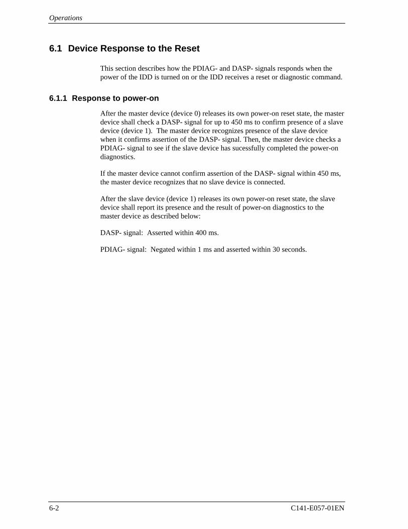
Operations
6-2 C141-E057-01EN
6.1 Device Response to the Reset
This section describes how the PDIAG- and DASP- signals responds when thepower of the IDD is turned on or the IDD receives a reset or diagnostic command.
6.1.1 Response to power-on
After the master device (device 0) releases its own power-on reset state, the masterdevice shall check a DASP- signal for up to 450 ms to confirm presence of a slavedevice (device 1). The master device recognizes presence of the slave devicewhen it confirms assertion of the DASP- signal. Then, the master device checks aPDIAG- signal to see if the slave device has sucessfully completed the power-ondiagnostics.
If the master device cannot confirm assertion of the DASP- signal within 450 ms,the master device recognizes that no slave device is connected.
After the slave device (device 1) releases its own power-on reset state, the slavedevice shall report its presence and the result of power-on diagnostics to themaster device as described below:
DASP- signal: Asserted within 400 ms.
PDIAG- signal: Negated within 1 ms and asserted within 30 seconds.
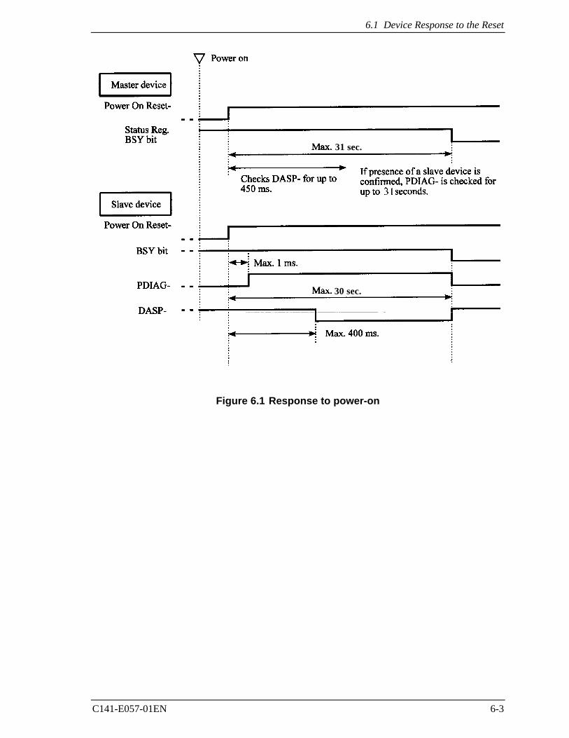
6.1 Device Response to the Reset
C141-E057-01EN 6-3
Figure 6.1 Response to power-on
31 sec.
30 sec.
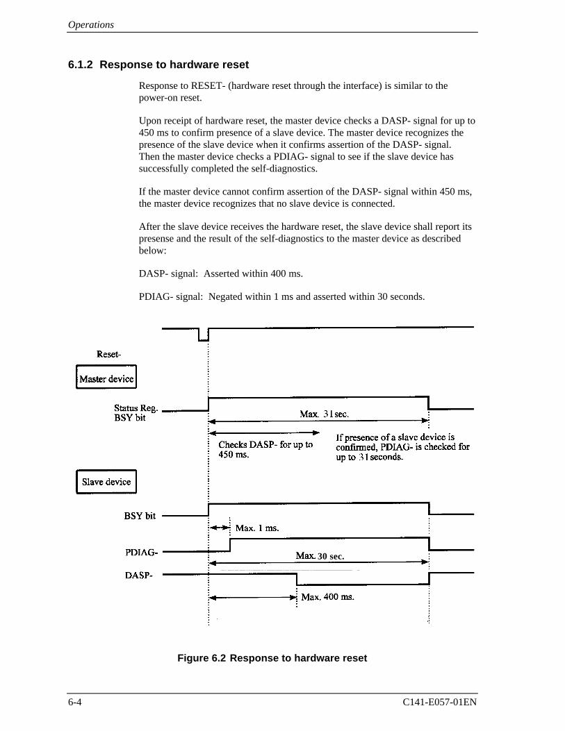
Operations
6-4 C141-E057-01EN
6.1.2 Response to hardware reset
Response to RESET- (hardware reset through the interface) is similar to thepower-on reset.
Upon receipt of hardware reset, the master device checks a DASP- signal for up to450 ms to confirm presence of a slave device. The master device recognizes thepresence of the slave device when it confirms assertion of the DASP- signal.Then the master device checks a PDIAG- signal to see if the slave device hassuccessfully completed the self-diagnostics.
If the master device cannot confirm assertion of the DASP- signal within 450 ms,the master device recognizes that no slave device is connected.
After the slave device receives the hardware reset, the slave device shall report itspresense and the result of the self-diagnostics to the master device as describedbelow:
DASP- signal: Asserted within 400 ms.
PDIAG- signal: Negated within 1 ms and asserted within 30 seconds.
Figure 6.2 Response to hardware reset
30 sec.
6.1 Device Response to the Reset
C141-E057-01EN 6-5
6.1.3 Response to software reset
The master device does not check the DASP- signal for a software reset. If aslave device is present, the master device checks the PDIAG- signal for up to 15seconds to see if the slave device has completed the self-diagnosis successfully.
After the slave device receives the software reset, the slave device shall report itspresense and the result of the self-diagnostics to the master device as describedbelow:
PDIAG- signal: negated within 1 ms and asserted within 30 seconds
When the IDD is set to a slave device, the IDD asserts the DASP- signal whennegating the PDIAG- signal, and negates the DASP- signal when asserting thePDIAG- signal.
Figure 6.3 Response to software reset
If the slave device is preset, PDIAG- is checked for upto 31 seconds.
30 sec.
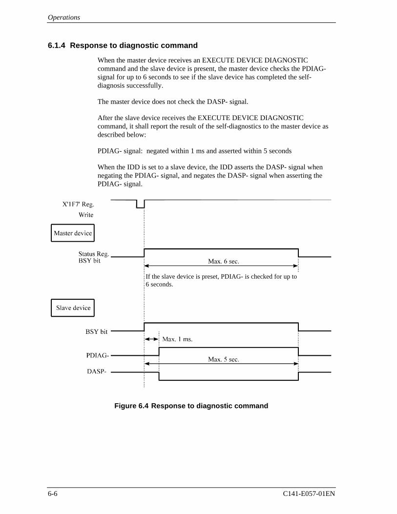
Operations
6-6 C141-E057-01EN
6.1.4 Response to diagnostic command
When the master device receives an EXECUTE DEVICE DIAGNOSTICcommand and the slave device is present, the master device checks the PDIAG-signal for up to 6 seconds to see if the slave device has completed the self-diagnosis successfully.
The master device does not check the DASP- signal.
After the slave device receives the EXECUTE DEVICE DIAGNOSTICcommand, it shall report the result of the self-diagnostics to the master device asdescribed below:
PDIAG- signal: negated within 1 ms and asserted within 5 seconds
When the IDD is set to a slave device, the IDD asserts the DASP- signal whennegating the PDIAG- signal, and negates the DASP- signal when asserting thePDIAG- signal.
Figure 6.4 Response to diagnostic command
If the slave device is preset, PDIAG- is checked for up to6 seconds.
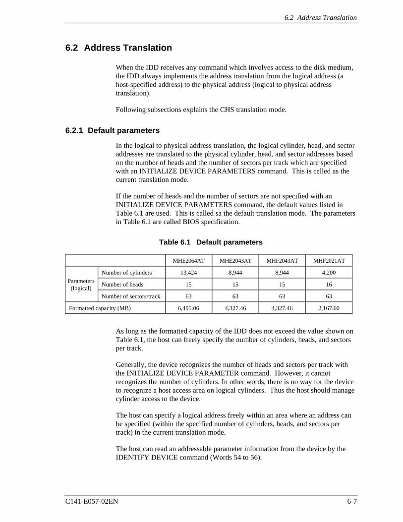
6.2 Address Translation
C141-E057-02EN 6-7
6.2 Address Translation
When the IDD receives any command which involves access to the disk medium,the IDD always implements the address translation from the logical address (ahost-specified address) to the physical address (logical to physical addresstranslation).
Following subsections explains the CHS translation mode.
6.2.1 Default parameters
In the logical to physical address translation, the logical cylinder, head, and sectoraddresses are translated to the physical cylinder, head, and sector addresses basedon the number of heads and the number of sectors per track which are specifiedwith an INITIALIZE DEVICE PARAMETERS command. This is called as thecurrent translation mode.
If the number of heads and the number of sectors are not specified with anINITIALIZE DEVICE PARAMETERS command, the default values listed inTable 6.1 are used. This is called sa the default translation mode. The parametersin Table 6.1 are called BIOS specification.
Table 6.1 Default parameters
MHE2064AT MHE2043AT MHF2043AT MHF2021AT
Number of cylinders 13,424 8,944 8,944 4,200
Number of heads 15 15 15 16
Number of sectors/track 63 63 63 63
Formatted capacity (MB) 6,495.06 4,327.46 4,327.46 2,167.60
As long as the formatted capacity of the IDD does not exceed the value shown onTable 6.1, the host can freely specify the number of cylinders, heads, and sectorsper track.
Generally, the device recognizes the number of heads and sectors per track withthe INITIALIZE DEVICE PARAMETER command. However, it cannotrecognizes the number of cylinders. In other words, there is no way for the deviceto recognize a host access area on logical cylinders. Thus the host should managecylinder access to the device.
The host can specify a logical address freely within an area where an address canbe specified (within the specified number of cylinders, heads, and sectors pertrack) in the current translation mode.
The host can read an addressable parameter information from the device by theIDENTIFY DEVICE command (Words 54 to 56).
Parameters(logical)
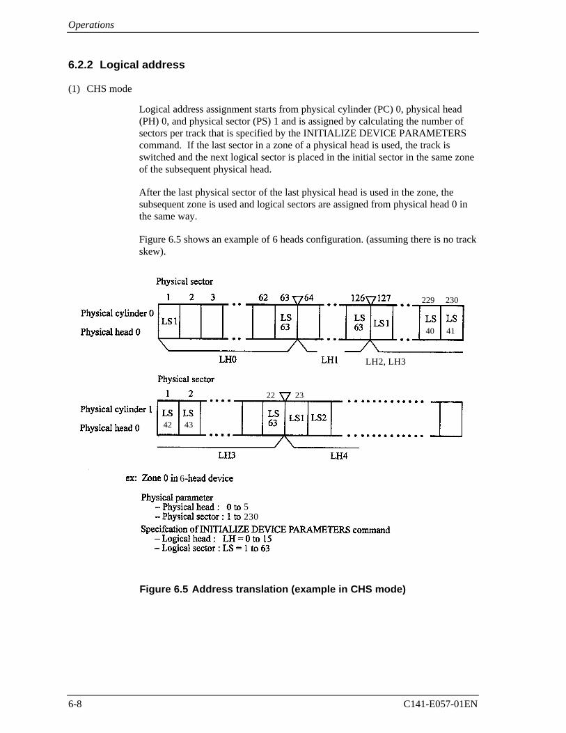
Operations
6-8 C141-E057-01EN
6.2.2 Logical address
(1) CHS mode
Logical address assignment starts from physical cylinder (PC) 0, physical head(PH) 0, and physical sector (PS) 1 and is assigned by calculating the number ofsectors per track that is specified by the INITIALIZE DEVICE PARAMETERScommand. If the last sector in a zone of a physical head is used, the track isswitched and the next logical sector is placed in the initial sector in the same zoneof the subsequent physical head.
After the last physical sector of the last physical head is used in the zone, thesubsequent zone is used and logical sectors are assigned from physical head 0 inthe same way.
Figure 6.5 shows an example of 6 heads configuration. (assuming there is no trackskew).
Figure 6.5 Address translation (example in CHS mode)
4342
2322
4140
230229
6
5230
LH2, LH3
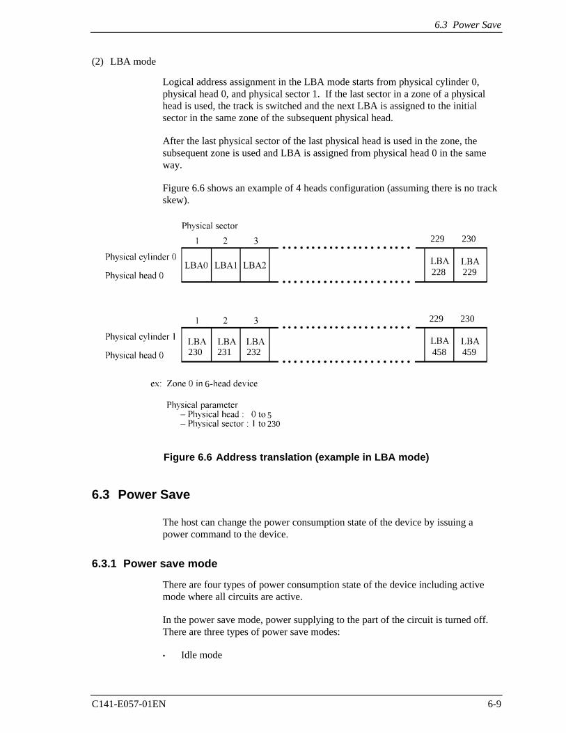
6.3 Power Save
C141-E057-01EN 6-9
(2) LBA mode
Logical address assignment in the LBA mode starts from physical cylinder 0,physical head 0, and physical sector 1. If the last sector in a zone of a physicalhead is used, the track is switched and the next LBA is assigned to the initialsector in the same zone of the subsequent physical head.
After the last physical sector of the last physical head is used in the zone, thesubsequent zone is used and LBA is assigned from physical head 0 in the sameway.
Figure 6.6 shows an example of 4 heads configuration (assuming there is no trackskew).
459
230
229228
229 230
230229
458232231230
6
5
Figure 6.6 Address translation (example in LBA mode)
6.3 Power Save
The host can change the power consumption state of the device by issuing apower command to the device.
6.3.1 Power save mode
There are four types of power consumption state of the device including activemode where all circuits are active.
In the power save mode, power supplying to the part of the circuit is turned off.There are three types of power save modes:
• Idle mode
Operations
6-10 C141-E057-01EN
• Standby mode
• Sleep mode
The drive moves from the Active mode to the idle mode by itself.
Regardless of whether the power down is enabled, the device enters the idle mode.The device also enters the idle mode in the same way after power-on sequence iscompleted.
And, the automatic power-down is executed if no command is coming for 30 min.(default)
(1) Active mode
In this mode, all the electric circuit in the device are active or the device is underseek, read or write operation.
A device enters the active mode under the following conditions:
• A command other than power commands is issued.
• A reset command is received.
(2) Idle mode
In this mode, circuits on the device is set to power save mode.
The device enters the Idle mode under the following conditions:
• After completion of power-on sequence.
• After completion of the command execution other than SLEEP and STANDBYcommands.
• After completion of the reset sequence
(3) Standby mode
In this mode, the VCM circuit is turned off and the spindle motor is stopped.
The device can receive commands through the interface. However if a commandwith disk access is issued, response time to the command under the standby modetakes longer than the active or Idle mode because the access to the disk mediumcannot be made immediately.
The drive enters the standby mode under the following conditions:
• A STANDBY or STANDBY IMMEDIATE command is issued in the activeor idle mode.
• When automatic power down sequence is enabled, the timer has elapsed.
• A reset is issued in the sleep mode.
6.4 Defect Management
C141-E057-01EN 6-11
When one of following commands is issued, the command is executed normallyand the device is still stayed in the standby mode.
• Reset (hardware or software)
• STANDBY command
• STANDBY IMMEDIATE command
• INITIALIZE DEVICE PARAMETERS command
• CHECK POWER MODE command
(4) Sleep mode
The power consumption of the drive is minimal in this mode. The drive entersonly the standby mode from the sleep mode. The only method to return from thestandby mode is to execute a software or hardware reset.
The drive enters the sleep mode under the following condition:
• A SLEEP command is issued.
Issued commands are invalid (ignored) in this mode.
6.3.2 Power commands
The following commands are available as power commands.
• IDLE
• IDLE IMMEDIATE
• STANDBY
• STANDBY IMMEDIATE
• SLEEP
• CHECK POWER MODE
6.4 Defect Management
Defective sectors of which the medium defect location is registered in the systemspace are replaced with spare sectors in the formatting at the factory shipment.
All the user space area are formatted at shipment from the factory based on thedefault parameters listed in Table 6.1.
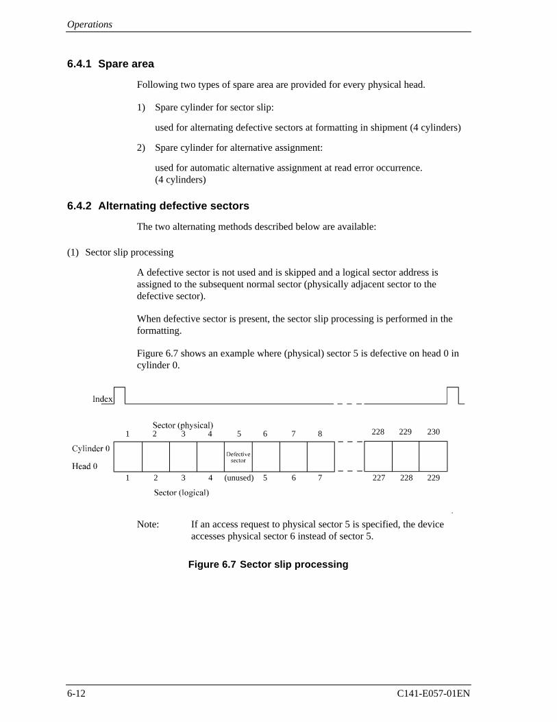
Operations
6-12 C141-E057-01EN
6.4.1 Spare area
Following two types of spare area are provided for every physical head.
1) Spare cylinder for sector slip:
used for alternating defective sectors at formatting in shipment (4 cylinders)
2) Spare cylinder for alternative assignment:
used for automatic alternative assignment at read error occurrence.(4 cylinders)
6.4.2 Alternating defective sectors
The two alternating methods described below are available:
(1) Sector slip processing
A defective sector is not used and is skipped and a logical sector address isassigned to the subsequent normal sector (physically adjacent sector to thedefective sector).
When defective sector is present, the sector slip processing is performed in theformatting.
Figure 6.7 shows an example where (physical) sector 5 is defective on head 0 incylinder 0.
If an access request to physical sector 5 is specified, the device accesses physical sector 6 instead of sector 5.
86 754321
(unused)
228 229 230
2292282277654321
Note: If an access request to physical sector 5 is specified, the deviceaccesses physical sector 6 instead of sector 5.
Figure 6.7 Sector slip processing
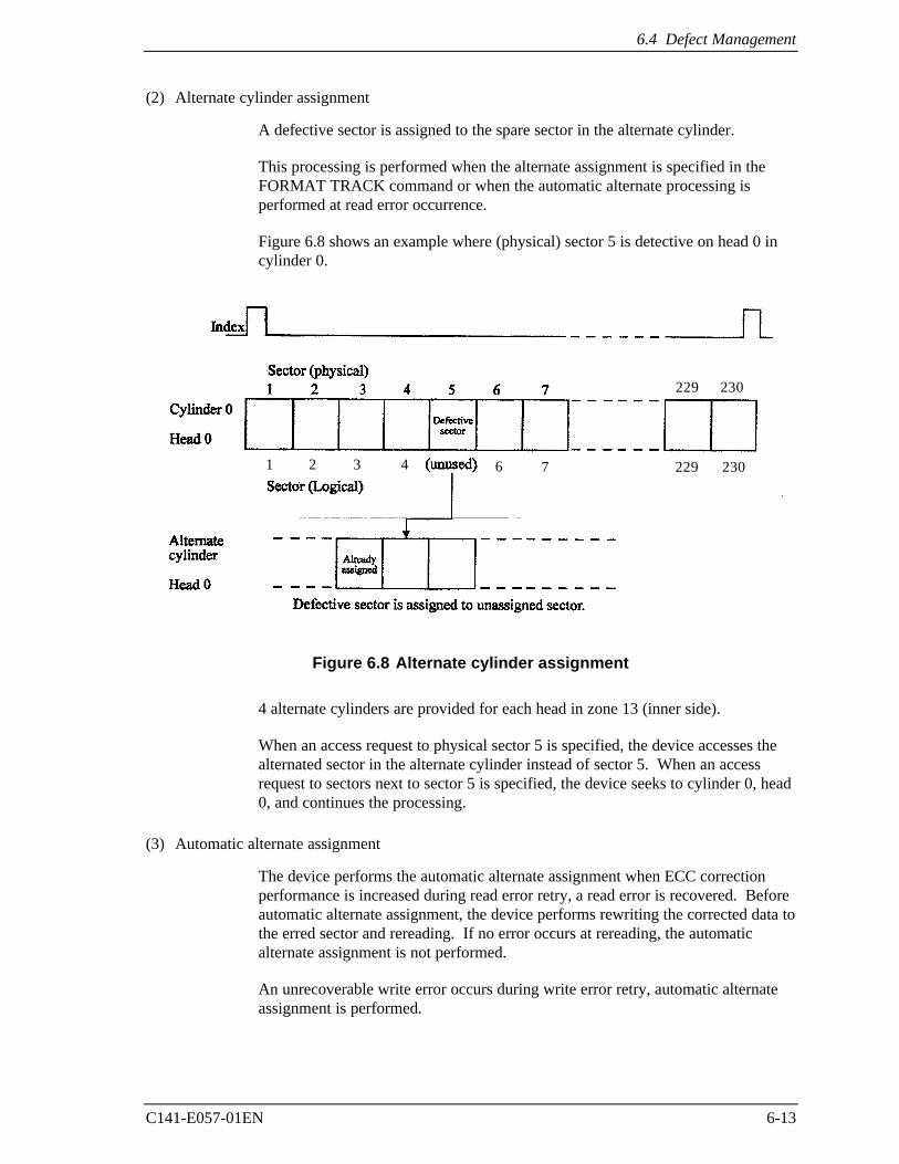
6.4 Defect Management
C141-E057-01EN 6-13
(2) Alternate cylinder assignment
A defective sector is assigned to the spare sector in the alternate cylinder.
This processing is performed when the alternate assignment is specified in theFORMAT TRACK command or when the automatic alternate processing isperformed at read error occurrence.
Figure 6.8 shows an example where (physical) sector 5 is detective on head 0 incylinder 0.
Figure 6.8 Alternate cylinder assignment
4 alternate cylinders are provided for each head in zone 13 (inner side).
When an access request to physical sector 5 is specified, the device accesses thealternated sector in the alternate cylinder instead of sector 5. When an accessrequest to sectors next to sector 5 is specified, the device seeks to cylinder 0, head0, and continues the processing.
(3) Automatic alternate assignment
The device performs the automatic alternate assignment when ECC correctionperformance is increased during read error retry, a read error is recovered. Beforeautomatic alternate assignment, the device performs rewriting the corrected data tothe erred sector and rereading. If no error occurs at rereading, the automaticalternate assignment is not performed.
An unrecoverable write error occurs during write error retry, automatic alternateassignment is performed.
230229
230229764321
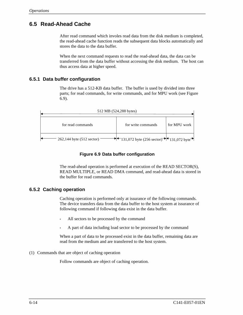
Operations
6-14 C141-E057-01EN
6.5 Read-Ahead Cache
After read command which involes read data from the disk medium is completed,the read-ahead cache function reads the subsequent data blocks automatically andstores the data to the data buffer.
When the next command requests to read the read-ahead data, the data can betransferred from the data buffer without accessing the disk medium. The host canthus access data at higher speed.
6.5.1 Data buffer configuration
The drive has a 512-KB data buffer. The buffer is used by divided into threeparts; for read commands, for write commands, and for MPU work (see Figure6.9).
for read commands for write commands for MPU work
512 MB (524,288 bytes)
262,144 byte (512 sector) 131,072 byte (256 sector) 131,072 byte
Figure 6.9 Data buffer configuration
The read-ahead operation is performed at execution of the READ SECTOR(S),READ MULTIPLE, or READ DMA command, and read-ahead data is stored inthe buffer for read commands.
6.5.2 Caching operation
Caching operation is performed only at issurance of the following commands.The device transfers data from the data buffer to the host system at issurance offollowing command if following data exist in the data buffer.
• All sectors to be processed by the command
• A part of data including load sector to be processed by the command
When a part of data to be processed exist in the data buffer, remaining data areread from the medium and are transferred to the host system.
(1) Commands that are object of caching operation
Follow commands are object of caching operation.
6.5 Read-Ahead Cache
C141-E057-01EN 6-15
• READ SECTOR (S)
• READ MULTIPLE
• READ DMA
When caching operation is disabled by the SET FEATURES command, nocaching operation is performed.
(2) Data that are object of caching operation
Follow data are object of caching operation.
1) Read-ahead data read from the medium to the data buffer after completion ofthe command that are object of caching operation.
2) Data transferred to the host system once by requesting with the command thatare object of caching operation (except for the cache invalid data by somereasons).
3) Remaining data in the data buffer (for write command) transferred from thehost system by the command that writes data onto the disk medium, such asthe WRITE SECTOR (S), WRITE DMA, WRITE MULTIPLE.
Followings are definition of in case that the write data is treated as a cache data.However, since the hit check at issurance of read command is performed to thedata buffer for read command prioritily, caching write data is limited to the casethat the hit check is missed at the data buffer for read command.
• When all data requested by the read command are stored in the data buffer forwrite command (hit all), the device transfers data from the data buffer forwrite command. At this time, the read-ahead operation to the data subsequentto the requested data is not performed.
• Even if a part of data requested by the read command are stored in the databuffer for write command (hit partially), all data are read from the diskmedium without transferring from the data buffer for write command.
(3) Invalidating caching data
Caching data in the data buffer is invalidated in the following case.
1) Following command is issued to the same data block as caching data.
− WRITE SECTOR(S)
− WRITE DMA
− WRITE MULTIPLE
2) Command other than following commands is issued (all caching data areinvalidated)
− READ SECTOR (S)
− READ DMA
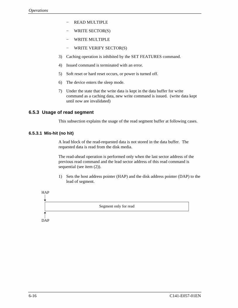
Operations
6-16 C141-E057-01EN
− READ MULTIPLE
− WRITE SECTOR(S)
− WRITE MULTIPLE
− WRITE VERIFY SECTOR(S)
3) Caching operation is inhibited by the SET FEATURES command.
4) Issued command is terminated with an error.
5) Soft reset or hard reset occurs, or power is turned off.
6) The device enters the sleep mode.
7) Under the state that the write data is kept in the data buffer for writecommand as a caching data, new write command is issued. (write data keptuntil now are invalidated)
6.5.3 Usage of read segment
This subsection explains the usage of the read segment buffer at following cases.
6.5.3.1 Mis-hit (no hit)
A lead block of the read-requested data is not stored in the data buffer. Therequested data is read from the disk media.
The read-ahead operation is performed only when the last sector address of theprevious read command and the lead sector address of this read command issequential (see item (2)).
1) Sets the host address pointer (HAP) and the disk address pointer (DAP) to thelead of segment.
Segment only for read
DAP
HAP
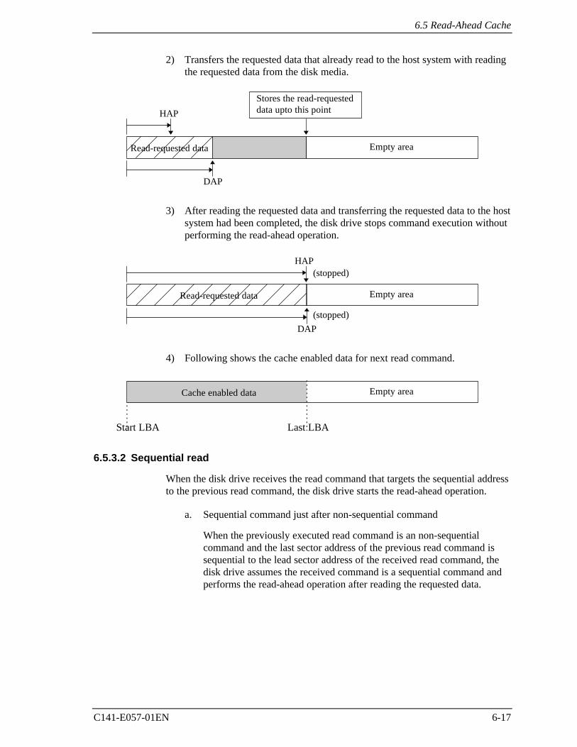
6.5 Read-Ahead Cache
C141-E057-01EN 6-17
2) Transfers the requested data that already read to the host system with readingthe requested data from the disk media.
Read-requested data
Stores the read-requesteddata upto this point
Empty area
DAP
HAP
3) After reading the requested data and transferring the requested data to the hostsystem had been completed, the disk drive stops command execution withoutperforming the read-ahead operation.
Read-requested data Empty area
DAP(stopped)
(stopped)HAP
4) Following shows the cache enabled data for next read command.
Cache enabled data Empty area
6.5.3.2 Sequential read
When the disk drive receives the read command that targets the sequential addressto the previous read command, the disk drive starts the read-ahead operation.
a. Sequential command just after non-sequential command
When the previously executed read command is an non-sequentialcommand and the last sector address of the previous read command issequential to the lead sector address of the received read command, thedisk drive assumes the received command is a sequential command andperforms the read-ahead operation after reading the requested data.
Start LBA Last LBA
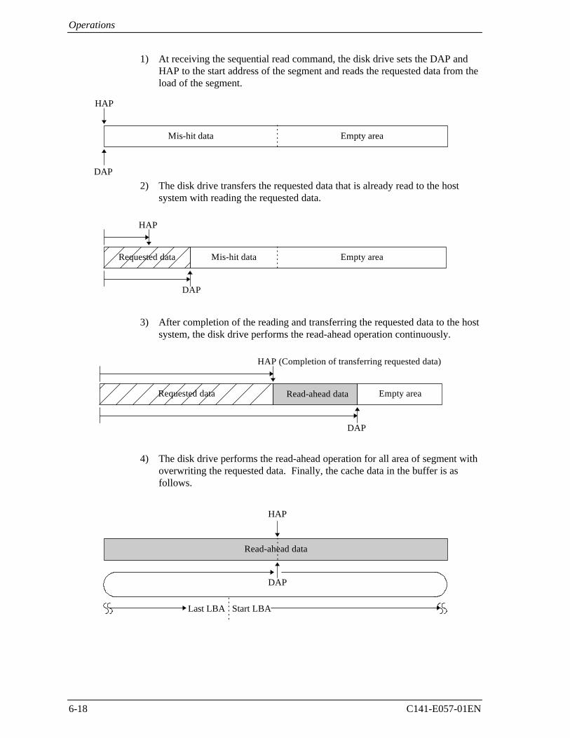
Operations
6-18 C141-E057-01EN
1) At receiving the sequential read command, the disk drive sets the DAP andHAP to the start address of the segment and reads the requested data from theload of the segment.
Empty areaMis-hit data
2) The disk drive transfers the requested data that is already read to the hostsystem with reading the requested data.
Requested data
DAP
HAP
Mis-hit data Empty area
3) After completion of the reading and transferring the requested data to the hostsystem, the disk drive performs the read-ahead operation continuously.
Requested data
DAP
HAP (Completion of transferring requested data)
Empty areaRead-ahead data
4) The disk drive performs the read-ahead operation for all area of segment withoverwriting the requested data. Finally, the cache data in the buffer is asfollows.
Start LBALast LBA
DAP
HAP
Read-ahead data
DAP
HAP
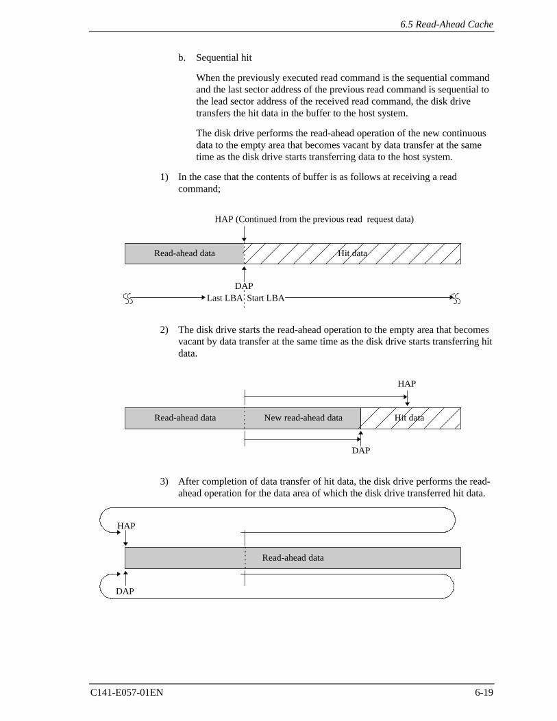
6.5 Read-Ahead Cache
C141-E057-01EN 6-19
b. Sequential hit
When the previously executed read command is the sequential commandand the last sector address of the previous read command is sequential tothe lead sector address of the received read command, the disk drivetransfers the hit data in the buffer to the host system.
The disk drive performs the read-ahead operation of the new continuousdata to the empty area that becomes vacant by data transfer at the sametime as the disk drive starts transferring data to the host system.
1) In the case that the contents of buffer is as follows at receiving a readcommand;
Start LBALast LBADAP
HAP (Continued from the previous read request data)
Hit dataRead-ahead data
2) The disk drive starts the read-ahead operation to the empty area that becomesvacant by data transfer at the same time as the disk drive starts transferring hitdata.
DAP
HAP
Hit dataNew read-ahead dataRead-ahead data
3) After completion of data transfer of hit data, the disk drive performs the read-ahead operation for the data area of which the disk drive transferred hit data.
Read-ahead data
HAP
DAP
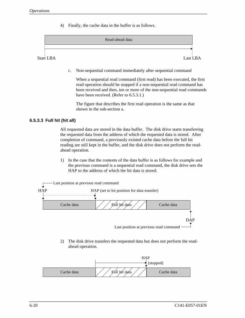
Operations
6-20 C141-E057-01EN
4) Finally, the cache data in the buffer is as follows.
Read-ahead data
c. Non-sequential command immediately after sequential command
When a sequential read command (first read) has been executed, the firstread operation should be stopped if a non-sequential read command hasbeen received and then, ten or more of the non-sequential read commandshave been received. (Refer to 6.5.3.1.)
The figure that describes the first read operation is the same as thatshown in the sub-section a.
6.5.3.3 Full hit (hit all)
All requested data are stored in the data buffer. The disk drive starts transferringthe requested data from the address of which the requested data is stored. Aftercompletion of command, a previously existed cache data before the full hitreading are still kept in the buffer, and the disk drive does not perform the read-ahead operation.
1) In the case that the contents of the data buffer is as follows for example andthe previous command is a sequential read command, the disk drive sets theHAP to the address of which the hit data is stored.
HAP (set to hit position for data transfer)
Last position at previous read command
Last position at previous read command
Cache dataFull hit dataCache data
2) The disk drive transfers the requested data but does not perform the read-ahead operation.
(stopped)HAP
Cache dataFull hit dataCache data
HAP
DAP
Last LBAStart LBA
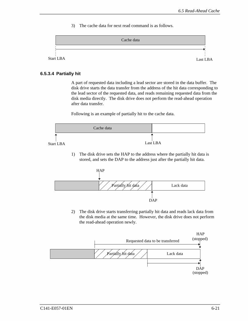
6.5 Read-Ahead Cache
C141-E057-01EN 6-21
3) The cache data for next read command is as follows.
Cache data
6.5.3.4 Partially hit
A part of requested data including a lead sector are stored in the data buffer. Thedisk drive starts the data transfer from the address of the hit data corresponding tothe lead sector of the requested data, and reads remaining requested data from thedisk media directly. The disk drive does not perform the read-ahead operationafter data transfer.
Following is an example of partially hit to the cache data.
Last LBA
Cache data
1) The disk drive sets the HAP to the address where the partially hit data isstored, and sets the DAP to the address just after the partially hit data.
HAP
DAP
Partially hit data Lack data
2) The disk drive starts transferring partially hit data and reads lack data fromthe disk media at the same time. However, the disk drive does not performthe read-ahead operation newly.
(stopped)HAP
(stopped)
Requested data to be transferred
DAP
Partially hit data Lack data
Start LBA
Last LBAStart LBA
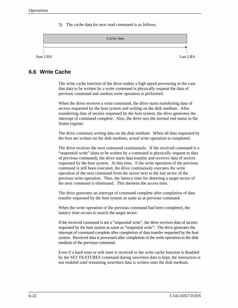
Operations
6-22 C141-E057-01EN
3) The cache data for next read command is as follows.
Cache data
6.6 Write Cache
The write cache function of the drive makes a high speed processing in the casethat data to be written by a write command is physically sequent the data ofprevious command and random write operation is performed.
When the drive receives a write command, the drive starts transferring data ofsectors requested by the host system and writing on the disk medium. Aftertransferring data of sectors requested by the host system, the drive generates theinterrupt of command complete. Also, the drive sets the normal end status in theStatus register.
The drive continues writing data on the disk medium. When all data requested bythe host are written on the disk medium, actual write operation is completed.
The drive receives the next command continuously. If the received command is a“sequential write” (data to be written by a command is physically sequent to dataof previous command), the drive starts data transfer and receives data of sectorsrequested by the host system. At this time, if the write operation of the previouscommand is still been executed, the drive continuously executes the writeoperation of the next command from the sector next to the last sector of theprevious write operation. Thus, the latency time for detecting a target sector ofthe next command is eliminated. This shortens the access time.
The drive generates an interrupt of command complete after completion of datatransfer requested by the host system as same as at previous command.
When the write operation of the previous command had been completed, thelatency time occurs to search the target sector.
If the received command is not a “sequential write”, the drive receives data of sectorsrequested by the host system as same as “sequential write”. The drive generates theinterrupt of command complete after completion of data transfer requested by the hostsystem. Received data is processed after completion of the write operation to the diskmedium of the previous command.
Even if a hard reset or soft reset is received or the write cache function is disabledby the SET FEATURES command during unwritten data is kept, the instruction isnot enabled until remaining unwritten data is written onto the disk medium.
Last LBAStart LBA
6.6 Write Cache
C141-E057-01EN 6-23
The drive uses a cache data of the last write command as a read cache data. Whena read command is issued to the same address after the write command (cachehit), the read operation to the disk medium is not performed.
If an error occurs during the write operation, the device retries the processing. If theerror cannot be recovered by retry, automatic alternate assignment is performed. Fordetails about automate alternate assignment, see item (3) of Section 6.4.2.
The write cache function is operated with the following command.
• WRITE SECTOR(S)
• WRITE MULTIPLE
• WRITE DMA
When Write Cache is permitted, the writing of the data transferredfrom the host by the abovementioned Write Cache permit commandinto the disk medium may not be completed at the moment a normalending interrupt has occurred.In case a non-recoverable error has occurred during receiving morethan one write command, it is difficult for the host to identify acommand that caused the error.(However, the error is not reported to the hose if an error at writinghas been processed normally.)Therefore, note that it is difficult for the host to retry an operationthat caused a non-recoverable error.

This page is intentionally left blank.
C141-E057-01EN GL-1
Glossary
Actuator
Head positioning assembly. The actuator consists of a voice coil motor and headarm. If positions the read-write (R-W) head.
AT bus
A bus between the host CPU and adapter board
ATA (AT Attachment) standard
The ATA standard is for a PC AT interface regulated to establish compatibilitybetween products manufactured by different vendors. Interfaces based on thisstandard are called ATA interfaces.
BIOS standard for drives
The BIOS standard collectively refers to the parameters defined by the host,which, for example, include the number of cylinders, the number of heads, and thenumber of sectors per track in the drive. The physical specifications of the drivedo not always correspond to these parameters.
The BIOS of a PC AT cannot make full use of the physical specifications of thesedrivers. To make the best use of these drives, a BIOS that can handle the standardparameters of these drives is required.
Command
Commands are instructions to input data to and output data from a drive.Commands are written in command registers.
Data block
A data block is the unit used to transfer data. A data block normally indicates asingle sector.
DE
Disk enclosure. The DE includes the disks, built-in spindle motor, actuator,heads, and air filter. The DE is sealed to protect these components from dust.
Master (Device 0)
The master is the first drive that can operate on the AT bus. The master is daisy-chained with the second drive which can operate in conformity with the ATAstandard.
Glossary
GL-2 C141-E057-01EN
MTBF
Mean time between failures. The MTBF is calculated by dividing the totaloperation time (total power-on time) by the number of failures in the disk driveduring operation.
MTTR
Mean time to repair. The MTTR is the average time required for a service personto diagnose and repair a faulty drive.
PIO (Programmed input-output)
Mode to transfer data under control of the host CPU
Positioning
Sum of the seek time and mean rotational delay
Power save mode
The power save modes are idle mode, standby mode, and sleep mode.
In idle mode, the drive is neither reading, writing, nor seeking data. In standbymode, the spindle motor is stopped and circuits other than the interface controlcircuit are sleeping. The drive enters sleep mode when the host issues the SLEEPcommand.
Reserved
Reserved bits, bytes, and fields are set to zero and unusable because they arereserved for future standards.
Rotational delay
Time delay due to disk rotation. The mean delay is the time required for half adisk rotation. The mean delay is the average time required for a head to reach asector after the head is positioned on a track.
Seek time
The seek time is the time required for a head to move from the current track toanother track. The seek time does not include the mean rotational delay.
Slave (Device 1)
The slave is a second drive that can operate on the AT bus. The slave is daisy-chained with the first drive operating in conformity with the ATA standard.
Glossary
C141-E057-01EN GL-3
Status
The status is a piece of one-byte information posted from the drive to the hostwhen command execution is ended. The status indicates the commandtermination state.
VCM
Voice coil motor. The voice coil motor is excited by one or more magnets. Inthis drive, the VCM is used to position the heads accurately and quickly.

This page is intentinally left blank.
C141-E057-01EN AB-1
Acronyms and Abbreviations
A
ABRT Abored commandAIC Automatic idle controlAMNF Address mark not foundATA AT attachmentAWG American wire gage
B
BBK Bad block detectedBIOS Basic input-output system
C
CORR Corrected dataCH Cylinder high registerCL Cylinder low registerCM Command registerCSR Current sense registerCSS Current start/stopCY Cylinder register
D
dBA dB A-scale weightingDE Disk enclosureDH Device/head registerDRDY Drive readyDRQ Ddata request bitDSC Drive seek completeDWF Drive write fault
E
ECC Error checking and correctionER Error registerERR Error
F
FR Feature register
H
HA Host adapter
HDD Hard disk drive
I
IDNF ID not foundIRQ14 Interrupt request 14
L
LED Light emitting diode
M
MB Mega-byteMB/S Mega-byte per secondsMPU Micro processor unit
P
PCA Printed circuit assemblyPIO Programed input-output
R
RLL Run-lrnght-limited
S
SA System areaSC Sector count registerSG Signal groundSN Sector number registerST Status register
T
TPI Track per inchesTRONF Track 0 not foundTyp Typical
U
UNC Uncorrectable ECC error
V
VCM Voice coil motor

This page is intentionally left blank.
C141-E057-01EN IN-1
Index
1-drive connection 2-42-drive connection 2-58/8 GCR 4-108/9 GCR decoder 4-13
A
Acceleration mode 4-21Acoustic noise 1-7Acoustic noise specification 1-7Active mode 6-10Actuator 2-3, 4-3Actuator motor control 4-19Adaptability 1-2Adaptive equalizer circuit 4-12ADC 4-17A/D converter 4-17Address translation 6-7, 6-8AGC circuit 4-12Air circulation system 2-4Air filter 4-3Alternate assignment, automatic 6-13Alternate cylinder assignment 6-13Alternate Status register 5-13Alternating defective sector 6-12Ambient temperature 3-5ATA 2-5ATA interface 2-4Attribute ID 5-56Attribute value for worst case so far 5-61Automatic alternate assignment 6-13Average positioning time 1-2
B
Block diagram of servo control circuit 4-14Blower 4-3Blower effect 2-4Breather filter 4-3BSY 5-11
C
Cable connection 3-7, 3-8Cable connector specification 3-8Caching operation 6-14Calibration 4-15CHECK POWER MODE 5-55Check sum 5-61
CHS mode 6-8Circuit configuration 4-4, 4-5Circulation filter 2-4, 4-3Combination of Identifier and Security level
5-69Command block register 5-8Command code 5-14, 5-71Command description 5-16Command processing 4-9Command protocol 5-73Command register 5-12Command that is object of caching operation
6-14Command without data transfer 5-77Compact 1-2Compensating open loop gain 4-8Connection to interface 1-2Connector location 3-7Content of security password 5-63Content of SECURITY SET PASSWORD
data 5-68Control block register 5-13Controller circuit 2-4, 4-4CORR 5-12CSEL setting 3-11Current attribute value 5-62Current fluctuation 1-6Current fluctuation when power is turned on
1-6Current requirement 1-6Cylinder High register 5-10Cylinder Low register 5-10
D
DAC 4-17D/A converter 4-17Data area 4-18Data assurance in event of power failure
1-9Data buffer 1-3Data buffer configuration 6-14Data corruption 3-6Data format version number 5-60Data register 5-8Data separator circuit 4-13Data-surface servo format 4-18
Index
IN-2 C141-E057-01EN
Data that is object of caching operation6-15
Data transfer rate 4-13Data transferring command 5-73, 5-75Data transfer timing 5-81DE 2-4Default parameter 6-7Defect management 6-11Device configuration 2-1Device connection 3-8Device connector 3-7Device Control register 5-13Device/Head register 5-10Device overview 1-1Device response to reset 6-2DF 5-12Diagnostic code 5-9Dimension 3-2Disk 2-2, 4-2Disk enclosure 2-4Disk media 2-3DMA data transfer command 5-78DMA data transfer protocol 5-78DRDY 5-11Driver 4-17Driver circuit 4-17DRQ 5-12DSC 5-12
E
Environmental specification 1-7ERR 5-12Error correction by ECC 1-3Error correction by retry 1-3Error posting 5-71Error rate 1-9Error register 5-8EXECUTE DEVICE DIAGNOSTIC 5-45Execution example of READ MULTIPLE
command 5-20Execution timing of self-calibration 4-8External magnetic field 3-6
F
Factory default setting 3-10Failure prediction capability flag 5-62Feature register function 5-57Feature register value 5-39, 5-57Features 1-2Features register 5-9Format of device attribute value data 5-59
Format of insurance failure threshold valuedata 5-60
Frame 3-4Frequency characteristics of programmable
filter 4-12Full hit 6-20Functions and performance 1-2
G
Gray code 4-19
H
HA 2-5Head 2-2, 4-2Head carriage 4-3Head structure 4-3High-speed transfer rate 1-2Hit all 6-20Host command 5-13
I
IDENTIFY DEVICE 5-31IDENTIFY DEVICE DMA 5-38IDLE 5-50IDLE IMMEDIATE 5-52Idle mode 6-10INITIALIZE DEVICE PARAMETERS
5-30Inner guard band 4-18Input voltage 1-5Installation condition 3-1Insurance failure threshold 5-58Interface 1-2, 5-1Interface signal 5-2Invalidating caching data 6-15I/O register 5-6
J
Jumper location 3-9Jumper setting 3-9
L
Large capacity 1-2LBA mode 6-9Limitation of side-mounting 3-4Logical address 6-8Logical interface 5-6
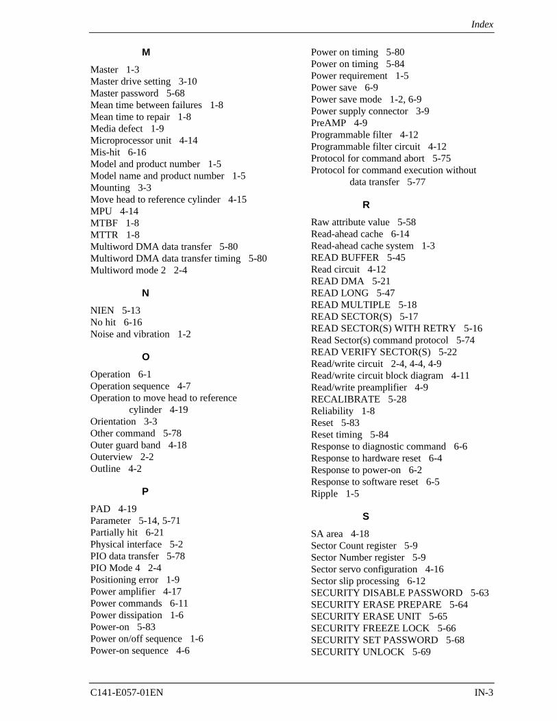
Index
C141-E057-01EN IN-3
M
Master 1-3Master drive setting 3-10Master password 5-68Mean time between failures 1-8Mean time to repair 1-8Media defect 1-9Microprocessor unit 4-14Mis-hit 6-16Model and product number 1-5Model name and product number 1-5Mounting 3-3Move head to reference cylinder 4-15MPU 4-14MTBF 1-8MTTR 1-8Multiword DMA data transfer 5-80Multiword DMA data transfer timing 5-80Multiword mode 2 2-4
N
NIEN 5-13No hit 6-16Noise and vibration 1-2
O
Operation 6-1Operation sequence 4-7Operation to move head to reference
cylinder 4-19Orientation 3-3Other command 5-78Outer guard band 4-18Outerview 2-2Outline 4-2
P
PAD 4-19Parameter 5-14, 5-71Partially hit 6-21Physical interface 5-2PIO data transfer 5-78PIO Mode 4 2-4Positioning error 1-9Power amplifier 4-17Power commands 6-11Power dissipation 1-6Power-on 5-83Power on/off sequence 1-6Power-on sequence 4-6
Power on timing 5-80Power on timing 5-84Power requirement 1-5Power save 6-9Power save mode 1-2, 6-9Power supply connector 3-9PreAMP 4-9Programmable filter 4-12Programmable filter circuit 4-12Protocol for command abort 5-75Protocol for command execution without
data transfer 5-77
R
Raw attribute value 5-58Read-ahead cache 6-14Read-ahead cache system 1-3READ BUFFER 5-45Read circuit 4-12READ DMA 5-21READ LONG 5-47READ MULTIPLE 5-18READ SECTOR(S) 5-17READ SECTOR(S) WITH RETRY 5-16Read Sector(s) command protocol 5-74READ VERIFY SECTOR(S) 5-22Read/write circuit 2-4, 4-4, 4-9Read/write circuit block diagram 4-11Read/write preamplifier 4-9RECALIBRATE 5-28Reliability 1-8Reset 5-83Reset timing 5-84Response to diagnostic command 6-6Response to hardware reset 6-4Response to power-on 6-2Response to software reset 6-5Ripple 1-5
S
SA area 4-18Sector Count register 5-9Sector Number register 5-9Sector servo configuration 4-16Sector slip processing 6-12SECURITY DISABLE PASSWORD 5-63SECURITY ERASE PREPARE 5-64SECURITY ERASE UNIT 5-65SECURITY FREEZE LOCK 5-66SECURITY SET PASSWORD 5-68SECURITY UNLOCK 5-69
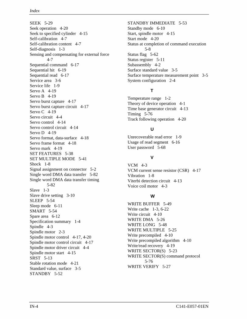
Index
IN-4 C141-E057-01EN
SEEK 5-29Seek operation 4-20Seek to specified cylinder 4-15Self-calibration 4-7Self-calibration content 4-7Self-diagnosis 1-3Sensing and compensating for external force
4-7Sequential command 6-17Sequential hit 6-19Sequential read 6-17Service area 3-6Service life 1-9Servo A 4-19Servo B 4-19Servo burst capture 4-17Servo burst capture circuit 4-17Servo C 4-19Servo circuit 4-4Servo control 4-14Servo control circuit 4-14Servo D 4-19Servo format, data-surface 4-18Servo frame format 4-18Servo mark 4-19SET FEATURES 5-38SET MULTIPLE MODE 5-41Shock 1-8Signal assignment on connector 5-2Single word DMA data transfer 5-82Single word DMA data transfer timing
5-82Slave 1-3Slave drive setting 3-10SLEEP 5-54Sleep mode 6-11SMART 5-54Spare area 6-12Specification summary 1-4Spindle 4-3Spindle motor 2-3Spindle motor control 4-17, 4-20Spindle motor control circuit 4-17Spindle motor driver circuit 4-4Spindle motor start 4-15SRST 5-13Stable rotation mode 4-21Standard value, surface 3-5STANDBY 5-52
STANDBY IMMEDIATE 5-53Standby mode 6-10Start, spindle motor 4-15Start mode 4-20Status at completion of command execution
5-8Status flag 5-62Status register 5-11Subassembly 4-2Surface standard value 3-5Surface temperature measurement point 3-5System configuration 2-4
T
Temperature range 1-2Theory of device operation 4-1Time base generator circuit 4-13Timing 5-76Track following operation 4-20
U
Unrecoverable read error 1-9Usage of read segment 6-16User password 5-68
V
VCM 4-3VCM current sense resistor (CSR) 4-17Vibration 1-8Viterbi detection circuit 4-13Voice coil motor 4-3
W
WRITE BUFFER 5-49Write cache 1-3, 6-22Write circuit 4-10WRITE DMA 5-26WRITE LONG 5-48WRITE MULTIPLE 5-25Write precompiled 4-10Write precompiled algorithm 4-10Write/read recovery 4-19WRITE SECTOR(S) 5-23WRITE SECTOR(S) command protocol
5-76WRITE VERIFY 5-27

This page is intentinally left blank.
C141-E057-02EN
Comment Form
We would appreciate your comments and suggestions regarding this manual.
Manual code C141-E057-02EN
Manual name MHE2064AT, MHE2043AT, MHF2043AT, MHF2021AT DISK DRIVEPRODUCT MANUAL
Please mark each item: E(Excellent), G(Good), F(Fair), P(Poor).
General appearance ( )Technical level ( )Organization ( )Clarity ( )Accuracy ( )
Illustration ( )Glossary ( )Acronyms & Abbreviations ( )Index ( )
Comments & Suggestions
List any errors or suggestions for improvement.
Page Line Contents
Please send this form to the address below. We will use your comments in planning future editions.
Address: Fujitsu Learning Media Limited22-7 Minami-Ooi 6-ChomeShinagawa-KuTokyo 140-0013JAPAN
Fax: 81-3-5762-8073
Organization:
Name:
C141-E057-02EN
C141-E057-02ENMHE2064/2043AT, MHF2043/2021AT DISK DRIVEPRODUCT MANUAL
MHE2064/2043AT, MHF2043/2021AT DISK DRIVEPRODUCT MANUAL