Embed Size (px)
Citation preview

LSI® SandForce® SF3700 Flash Controller
Embargo Until November 18, 2013, 6:00 am PST (GMT-8)
November 2013

2 Copyright 2013 LSI Inc.
Embargo Until November 18, 2013, 6:00 am PST (GMT-8)
NAND Flash Evolution: Capabilities & Characteristics
Time
Flash
Benefits
Flash
Challenges
Growing Dependence on Flash Controller to Close Gap
Benefits
• Lower $/GB Cost
• Higher Capacity
• Higher Unit Volume
Challenges
• Shorter Endurance
• Performance w/less die
• Lower Reliability
• Higher ECC Req.
• Evolving Flash Types
34nm
24/25nm
20/19nm
1x/1ynm
All flash is different and changes every 18 months!
– Endurance, Reliability, Performance, Interface
10K
3K
1K
Previous Generation
Current Generation
Next Generation
Program / Erase Cycles
5x nm MLC
3x nm MLC
2x nm MLC
3-bit per cell
Error Correction
Requirements (bits/KB)
4 12
40
60

3 Copyright 2013 LSI Inc.
Embargo Until November 18, 2013, 6:00 am PST (GMT-8)
Introducing the LSI SandForce SF3700 Flash Controller
Newly engineered to solve the latest challenges of NAND Flash
Designed for both Enterprise and Client markets
Provides native PCIe and SATA interfaces in a single ASIC
Builds on the award winning technology of current SandForce Flash Controllers
OEM SSD manufacturers bringing up designs now; mass production expected 1H’14

4 Copyright 2013 LSI Inc.
Embargo Until November 18, 2013, 6:00 am PST (GMT-8)
SF3700 Flash Controller
SATA III, 6Gb/s AHCI
Dual AES-256 Buffer SHIELD™
Programmable NAND Interface
Toggle / ONFI
9 channels SLC / eMLC /
MLC / TLC
2y, 1x, 1y nm
Intelligent Wear
Leveling
SMART
GPIO
RAISE™
PH
Y
Front-End Processor
DuraWrite™
Garbage Collection
Read Disturb Management
Back-End Controller
MAP Management
Unit
Front-End I/F Core Back-End I/F
PCIe Gen2 x4 NVMe & AHCI
New modular and flexible design best supports evolving flash types
Solves NAND Issues
• Evolving Flash Types
Modular/Flexible Architecture Enables:
• Single ASIC with multiple host interfaces
• Ability to support new host interface features
• Support for new Flash modes
• Continuous innovation through product life
Benefits
• Faster time to market
• Better cost and inventory management
• Extended product life
• Richer product portfolio
40nm Process

5 Copyright 2013 LSI Inc.
Embargo Until November 18, 2013, 6:00 am PST (GMT-8)
SF3700 Product Family
SF3759
Enterprise Caching
Enterprise Storage Scalable PCIe
Full Enterprise Feature Set
SF3729
Mainstream Client SATA + x2 PCIe
SF3739
Enthusiast Client
Value Enterprise x4 PCIe + Full Power Fail
SF3719
Entry Client SATA + x2 PCIe

6 Copyright 2013 LSI Inc.
Embargo Until November 18, 2013, 6:00 am PST (GMT-8)
SF3700 Performance Random and Sequential
Solves NAND Issues
• Performance w/less die
PCIe Performance SF3700 (256GB) MLC Samsung XP941 (512GB) MLC*
Testing Conditions
Early FW FOB
100% Entropy
LSI Spec 8GB Span
100% Entropy
3rd Party Review FOB
Mfg. Spec FOB
Rnd Read (IOPS) 150K 82-99K 122K
Rnd Writes (IOPS) 81K 60-70K 72K
Seq Reads (MB/s) 1450 1800 986-1134 1400
Seq Writes (MB/s) 1800 677-935 970
These SF3700 results assume 100% entropy (worst case)
Optimizing performance as Flash geometry shrinks
SATA Performance SF3700 (256GB) MLC Samsung 840 Pro (256GB) MLC*
Testing Conditions
Early FW FOB
100% Entropy
LSI Spec 8GB Span
100% Entropy
3rd Party Review FOB
Mfg. Spec FOB
Rnd Read (IOPS) 90K 94K 91K 100K
Rnd Writes (IOPS) 46K 70K 78K
Seq Reads (MB/s) 562 550 413 540
Seq Writes (MB/s) 502 373 450
*Sources: http://www.anandtech.com/show/6328/samsung-ssd-840-pro-256gb-review/1, http://www.thessdreview.com/our-reviews/samsung-xp941-m-2-pcie-ssd-review-512gb/, http://www.samsung.com/global/business/semiconductor/news-events/press-releases/detail?newsId=12921

7 Copyright 2013 LSI Inc.
Embargo Until November 18, 2013, 6:00 am PST (GMT-8)
SF3700 Latency Predictable latency is key for datacenters
Solves NAND Issues
• Performance w/less die
Flash performance trades off Latency vs. IOPS: IOPS = QD/latency
0
20
40
60
80
100
120
0 200 400 600 800 1000
To
tal K
IOP
S
Read Latency (usec)
Avg. Read Latency vs. KIOPs with increasing QD
70%R/30%W, 64 die, 28% OP
SF3700* Competing Low-latency SSD
50 55 60 65 70 75 80 85 90 95
100
0 25 50 75 100 125 150 175 200
Cu
mu
lati
ve
%
of
Op
era
tio
ns
Write Latency (usec)
Write Latency Distribution 70%R/30%W, 64 die, 28% OP, QD=32
SF3700*
99.99% < 170 usec
* Performance Model
Write latency should hit 100% as quickly as possible
Read latency should stay vertical as long as possible

8 Copyright 2013 LSI Inc.
Embargo Until November 18, 2013, 6:00 am PST (GMT-8)
DuraWrite™ Data Reduction – SF3700 Improvements
Enhanced version of field-proven LSI SandForce data reduction technology
– Higher data reduction capability
– Improved block picking and garbage collection
Provides numerous advantages for typical data
Includes many recursive benefits
Solves NAND Issues
• Shorter Endurance
• Performance w/less die

9 Copyright 2013 LSI Inc.
Embargo Until November 18, 2013, 6:00 am PST (GMT-8)
SHIELD™ Error Correction Technology Advanced Low-density Parity Check (LDPC) for Flash Storage
The strongest SSD ECC available today
Applies progressively stronger decoding methods as necessary
Hard-decision LDPC
DSP-aided Soft-decision
LDPC
Adaptive Code Rate
Multi-level Error
Correction Schema
Intelligent Noise
Handling
Parallel LDPC Engines with Specialized
H/W
Proven LDPC Experience
Don’t be fooled by other LDPC solutions
SHIELD technology uniquely combines a
number of features and correction techniques
Solves NAND Issues
• Lower Reliability
• Higher ECC Req.
• Evolving Flash Types

10 Copyright 2013 LSI Inc.
Embargo Until November 18, 2013, 6:00 am PST (GMT-8)
SHIELD Error Correction Technology Adaptive Code Rate
Flash at beginning of life (BOL) is more robust; requires less ECC
Leverages DuraWrite™ Flash Translation Layer to dynamically change Spare area
Gives extra spare ECC field to OP and increase performance / endurance
– Up to 3% more OP (as much as 41% more total OP*)
As drive reaches end of life (EOL), SHIELD increases ECC to maintain readability and increase endurance beyond NAND spec
User Data and OP Space
Spare NAND Page
ECC Conventional Error Correction:
Stores fixed ECC in spare field
User Data and OP Space
Spare NAND Page
ECC Adaptive ECC (BOL):
Stores ECC in a portion of spare field and increase OP
User Data and OP Space
Spare NAND Page
ECC Adaptive ECC (EOL):
Stores ECC in spare field and uses some of the NAND page
Adaptive ECC allows for more free space
@ BOL = Higher Performance /
Endurance
Solves NAND Issues
• Lower Reliability
• Higher ECC Req.
• Evolving Flash Types
*Based on physical OP change = (3 / 7.37)
11 Copyright 2013 LSI Inc.
Embargo Until November 18, 2013, 6:00 am PST (GMT-8)
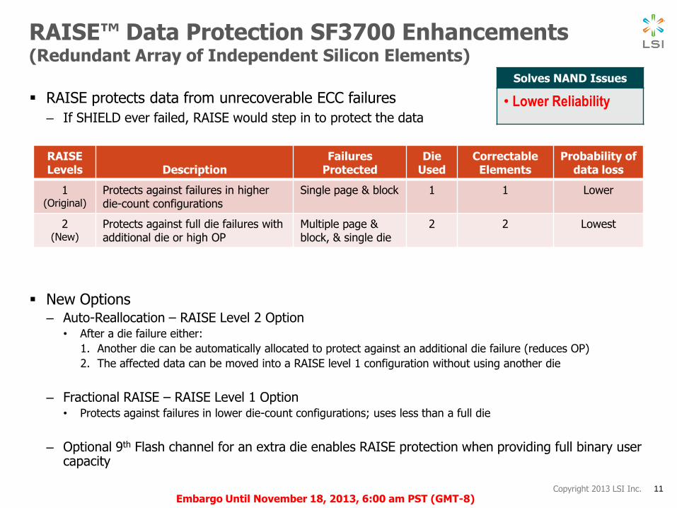
RAISE™ Data Protection SF3700 Enhancements (Redundant Array of Independent Silicon Elements)
New Options – Auto-Reallocation – RAISE Level 2 Option
• After a die failure either:
1. Another die can be automatically allocated to protect against an additional die failure (reduces OP)
2. The affected data can be moved into a RAISE level 1 configuration without using another die
– Fractional RAISE – RAISE Level 1 Option • Protects against failures in lower die-count configurations; uses less than a full die
– Optional 9th Flash channel for an extra die enables RAISE protection when providing full binary user capacity
RAISE protects data from unrecoverable ECC failures
– If SHIELD ever failed, RAISE would step in to protect the data
Solves NAND Issues
• Lower Reliability
RAISE Levels Description
Failures Protected
Die Used
Correctable Elements
Probability of data loss
1 (Original)
Protects against failures in higher die-count configurations
Single page & block 1 1 Lower
2 (New)
Protects against full die failures with additional die or high OP
Multiple page & block, & single die
2 2 Lowest

12 Copyright 2013 LSI Inc.
Embargo Until November 18, 2013, 6:00 am PST (GMT-8)
Key Feature Summary
SF3700 Features User Benefits Flash Challenge Solved
• DuraWrite Enhancements • Higher Performance
• Longer Endurance
• Shorter Endurance
• Performance w/less die
• SHIELD Error Recovery • Higher Data Reliability
• Longer Endurance
• Lower Reliability
• Higher ECC Req.
• Evolving Flash Types
• New RAISE Levels and
Options
• Higher Data Protection
• Lower Reliability
• Flexible, modular architecture • Adaptability to future Flash • Evolving Flash Types
• Low, predictable latency • Consistent performance to
meet SLAs
• Performance w/less die
Engineered to solve the challenges of NAND Flash

13 Copyright 2013 LSI Inc.
Embargo Until November 18, 2013, 6:00 am PST (GMT-8)
SF3700 Reference Design SSDs
Fastest time-to-market with largest selection of flash vendors
Widest selection of form factors (standard / custom)
DRAM-Less design enables many other options
Directly engage with flash, drive, system OEMs & cloud service providers
2.5” SATA 6Gb/s
PCIe Gen2 x2
M.2 2280 SATA 6Gb/s
PCIe Gen2 x2 HHHL
PCIe Gen2 x2/x4
Flash Controllers
Doc & Support
Turnkey Reference Designs
Mfg & Test Tools
Firmware
LSI Enables the Entire Production Flow

14 Copyright 2013 LSI Inc.
Embargo Until November 18, 2013, 6:00 am PST (GMT-8)
LSI DuraClass™ Technology Optimizes Data Storage
Reliability – RAISE™ and SHIELD™ technology, End-to-End protection
Endurance – DuraWrite™ technology, MLC flash in Enterprise
Single-Chip – DRAM-less, super dense designs
Performance – Low latency with low CPU utilization
Extensive Manageability – Simple IT management
Drive Level Security – Safe Data Storage without Compromises
Capacity Density – More bits in small systems
System Efficiency – Best total performance per watt
Flexible Power Management – Increased battery life

15 Copyright 2013 LSI Inc.
Embargo Until November 18, 2013, 6:00 am PST (GMT-8)
LSI SandForce SF3700 Flash Controller
Newly engineered to solve the challenges of NAND Flash
Expanding award-winning DuraClass technology
– SHIELD advanced LDPC error correction
– DuraWrite data reduction improvements
– RAISE data protection enhancements
Continuing a proven business model
– Complete turnkey solutions
– Wide Flash memory support
Accelerating the Growth of SSD Deployments
RAISE Enhancements
New RAISE Level 2
Auto-reallocation
Fractional RAISE

16 Copyright 2013 LSI Inc.
Embargo Until November 18, 2013, 6:00 am PST (GMT-8)
Live Demonstrations
LSI will be running live demonstrations of the SF3700 at two events:
– Supercomputing 2013
• November 18-21; Denver, Colorado
– Accelerating Innovation Summit 2013
• November 19-21; San Jose, California
LSI partners showing SF3700 demonstrations at AIS include:
Demonstrations include Toshiba A19nm and Micron 20nm Flash

Follow SandForce
T R A N S F O R M I N G D A T A S T O R A G E
LSI, the LSI & Design logo, DuraClass, DuraWrite, SandForce, SandForce Driven, SHIELD, and RAISE are the trademarks or registered trademarks of LSI Corporation in the United States and/or other countries. All other brand or product names may be trademarks or registered trademarks of their respective companies.