Embed Size (px)
Citation preview

SMSC DS – LPC47N252 Rev. 09/06/2000
LPC47N252PRELIMI NARY
_
Advanced Notebook I/O Controllerwith On-Board FLASH
FEATURES
§ 3.3V Operation with 5V Tolerant Buffers§ ACPI 1.0b , PC99/PC2001 Compliant
§ LPC Interface with Clock Run Support
− Serial IRQ Interface Compatible withSerialized IRQ Support for PCI Systems
− 15 Direct IRQs− Four 8-Bit DMA Channels− ACPI SCI Interface− nSMI− Shadowed write only registers
§ Internal 64K Flash ROM
− Programmed From Direct Parallel Interface,8051, or LPC Host
− 2k-Byte Lockable Boot Block− Can be Programed Without 8051
Intervention§ Three Power Planes
− Low Standby Current in Sleep Mode− Intelligent Auto Power Management for
Super I/O
§ ACPI Embedded Controller Interface§ Configuration Register Set Compatible with ISA
Plug-and-Play Standard (Version 1.0a)
§ High-Performance Embedded 8051 Keyboardand System Controller
− Provides System Power Management− System Watch Dog Timer (WDT)− 8042 Style Host Interface− Supports Interrupt and Polling Access− 256 Bytes Data RAM− On-Chip Memory-Mapped Control Registers− Access to RTC and CMOS Registers− Up to 16x8 Keyboard Scan Matrix− Two 16 Bit Timer/Counters− Integrated Full-Duplex Serial Port Interface− Eleven 8051 Interrupt Sources− Thirty-Two 8-Bit, Host/8051 Mailbox
Registers− Thirty-six Maskable Hardware Wake-Up
Events
− Fast GATEA20− Fast CPU_RESET− Multiple Clock Sources and Operating
Frequencies− IDLE and SLEEP Modes− Fail-Safe Ring Oscillator
§ Advanced Infrared Communications Controller(IrCC 2.0)
− IrDA V1.2 (4Mbps), HPSIR, ASKIR,Consumer IR Support
− Two IR Ports− Relocatable Base I/O Address
§ Real-Time Clock
− MC146818 and DS1287 Compatible− 256 Bytes of Battery Backed CMOS in Two
128-Byte Banks− 128 Bytes of CMOS RAM Lockable in 4x32
Byte Blocks− 12 and 24 Hour Time Format− Binary and BCD Format− <2µA Standby Current (typ)
§ Two 8584-Style ACCESS.Bus Controllers
− 8051 Controlled Logic Allows ACCESS.BusMaster or Slave Operation
− ACCESS.Bus Controllers are FullyOperational on Standby Power
− 2 Sets of Dedicated Pins perACCESS.BusController
§ Four independent Hardware Driven PS/2 Ports§ 83 General Purpose I/O Pins
− 36 Maskable Hardware Wake-EventCapable
− 18 Programmable Open-Drain/Push-PullOutputs
− 16 Mapped into 8051 SFR Space− 24 LPC/8051-Addressable
§ Three Programmable Pulse-Width ModulatorOutputs
− Independent Clock Rates− 6 Bit Duty Cycle Granularity

SMSC DS - LPC47N252 Page 2 Rev. 09/06/2000
− VCC1 and VCC2 operation mode� Dual Fan Tachometer Inputs� 2.88MB Super I/O Floppy Disk Controller
− Relocatable to 480 Different Base I/OAddresses
− 15 IRQ Options− 4 DMA Options− Open-Drain/Push-Pull Configurable Output
Drivers− Licensed CMOS 765B Floppy Disk
Controller− Advanced Digital Data Separator− Software and Register Compatible with
SMSC's Proprietary 82077AA CompatibleCore
− Low Power CMOS Design with SophisticatedPower Control Circuitry (PCC) IncludingMultiple Powerdown Modes for ReducedPower Consumption
− Supports Two Floppy Drives on the FDDInterface and Two Floppy Drives on theParallel Port Interface
− 12 mA FDD Interface Cable Drivers withSchmitt Trigger Inputs
� Licensed CMOS 765B Floppy Disk ControllerCore
− Supports Vertical Recording Format− 16-Byte Data FIFO− 100% IBM Compatibility− Detects All Overrun and Underrun
Conditions− 12 mA Drivers and Schmitt Trigger Inputs− DMA Enable Logic− Data Rate and Drive Control Registers
� Enhanced Digital Data Separator
− Low Cost Implementation− No Filter Components Required− 2 Mbps, 1 Mbps, 500 Kbps, 300 Kbps, 250
Kbps Data Rates− Programmable Precompensation Modes
� Multi-Mode Parallel Port with ChiProtect
− Standard Mode IBM PC/XT, PC/AT, andPS/2 Compatible Bi-directional Parallel Port
− Enhanced Parallel Port EPP 1.7 and EPP1.9 Compatible (IEEE 1284 Compliant)
− IEEE 1284 Compliant Enhanced CapabilitiesPort (ECP)
− ChiProtect Circuitry to Prevent PrinterPower-On Damage
− Relocatable to 480 Different Base I/OAddresses
− 15 IRQ Options− 4 DMA Options− Microsoft and HP compatible High Speed
Mode− Floppy Disk Interface on Parallel Port− 8051-Controlled Parallel Port Mode
� Serial Port
− High-Speed NS16550A-Compatible UARTwith 16-Byte Send/Receive FIFOs
− Programmable Baud Rate Generator− Modem Control Circuitry Including 230k and
460k Baud− Relocatable to 480 Different Base I/O
Addresses− 15 IRQ Options
ORDERING INFORMATIONOrder Numbers:
LPC47N252-SG for 208 Pin FBGA PackageLPC47N252-SD for 208 Pin TQFP Package

SMSC DS – LPC47N252 Page 3 Rev. 09/06/2000
GENERAL DESCRIPTION
The LPC47N252 is a 208-pin 3.3V LPC-based ACPI 1.0 and PC99/PC2001 compliant Notebook I/O Controller withFast Infrared for mobile applications. See FIGURE 2 – LPC47N252 BLOCK DIAGRAM.
The LPC47N252 incorporates a high-performance 8051-based keyboard controller; a 64k byte internal Flash ROM,four PS/2 ports; a real-time clock; SMSC's true CMOS 765B floppy disk controller with advanced digital dataseparator and 16-byte data FIFO; an NS16C550A-compatible UART, SMSC’s advanced Infrared CommunicationsController (IrCC 2.0) with a UART and a Synchronous Communications Engine to provide IrDA v1.1 (Fast IR)capabilities; one Multi-Mode parallel port with ChiProtect circuitry plus EPP and ECP support; two 8584-style AccessBus controllers with two Sets of Dedicated Pins per ACCESS.Bus Controller; a Serial IRQ peripheral agent interface;an ACPI Embedded Controller Interface; General Purpose I/O pins including eight pass through ports; threeindependently programmable pulse width modulators; two-floppy direct drive support; and maskable hardware wake-up events.
The true CMOS 765B core provides 100% compatibility with IBM PC/XT and PC/AT architectures in addition toproviding data overflow and underflow protection. The SMSC advanced digital data separator incorporates SMSC'spatented data separator technology, allowing for ease of testing and use. The parallel port is compatible with IBMPC/AT architecture, as well as EPP and ECP. The 8051 controller can also take control of the parallel port interfaceto provide remote diagnostics or “Flashing” of the Flash memory.
The LPC47N252 has three separate power planes to provide “instant on” and system power management functions.Additionally, the LPC47N252 incorporates sophisticated power control circuitry (PCC). The PCC supports multiplelow power down modes. Wake-up events and ACPI-related functions are supported through the SCI Interface.
The LPC47N252’s configuration register set is compatible with the ISA Plug-and-Play Standard (Version 1.0a) andprovides the functionality to support Windows '95.The legacy host Super I/O Configuration and Alternate Super I/OConfiguration decode ranges comply with the Low Pin Count Interface Specification, Revision 1.0.
Through internal configuration registers, each of the LPC47N252's logical device's I/O address, DMA channel andIRQ channel may be programmed. There are 480 I/O address location options, 15 IRQ options, and four DMAchannel options for each logical device.
The LPC47N252 does not require any external filter components and is, therefore, easy to use and offers lowersystem cost and reduced board area. The LPC47N252 is software and register compatible with SMSC's proprietary82077AA core.
© STANDARD MICROSYSTEMS CORPORATION (SMSC) 2000
80 Arkay DriveHauppauge, NY 11788(631) 435-6000FAX (631) 273-3123
Standard Microsystems is a registered trademark of Standard Microsystems Corporation, and SMSC, Ultra I/O, ChiProtect, and Multi-Mode aretrademarks of Standard Microsystems Corporation. Product names and company names are the trademarks of their respective holders. Circuitdiagrams utilizing SMSC products are included as a means of illustrating typical applications; consequently complete information sufficient forconstruction purposes is not necessarily given. Although the information has been checked and is believed to be accurate, no responsibility isassumed for inaccuracies. SMSC reserves the right to make changes to specifications and product descriptions at any time without notice. Contactyour local SMSC sales office to obtain the latest specifications before placing your product order. The provision of this information does not convey tothe purchaser of the semiconductor devices described any licenses under the patent rights of SMSC or others. All sales are expressly conditional onyour agreement to the terms and conditions of the most recently dated version of SMSC's standard Terms of Sale Agreement dated before the date ofyour order (the "Terms of Sale Agreement"). The product may contain design defects or errors known as anomalies which may cause the product'sfunctions to deviate from published specifications. Anomaly sheets are available upon request. SMSC products are not designed, intended,authorized or warranted for use in any life support or other application where product failure could cause or contribute to personal injury or severeproperty damage. Any and all such uses without prior written approval of an Officer of SMSC and further testing and/or modification will be fully at therisk of the customer. Copies of this document or other SMSC literature, as well as the Terms of Sale Agreement, may be obtained by visiting SMSC’swebsite at http://www.smsc.com.
SMSC DISCLAIMS AND EXCLUDES ANY AND ALL WARRANTIES, INCLUDING WITHOUT LIMITATION ANY AND ALL IMPLIED WARRANTIESOF MERCHANTABILITY, FITNESS FOR A PARTICULAR PURPOSE, TITLE, AND AGAINST INFRINGEMENT, AND ANY AND ALLWARRANTIES ARISING FROM ANY COURSE OF DEALING OR USAGE OF TRADE.
IN NO EVENT SHALL SMSC BE LIABLE FOR ANY DIRECT, INCIDENTAL, INDIRECT, SPECIAL, PUNITIVE, OR CONSEQUENTIAL DAMAGES,OR FOR LOST DATA, PROFITS, SAVINGS OR REVENUES OF ANY KIND; REGARDLESS OF THE FORM OF ACTION, WHETHER BASED ONCONTRACT, TORT, NEGLIGENCE OF SMSC OR OTHERS, STRICT LIABILITY, BREACH OF WARRANTY, OR OTHERWISE; WHETHER ORNOT ANY REMEDY IS HELD TO HAVE FAILED OF ITS ESSENTIAL PURPOSE; AND WHETHER OR NOT SMSC HAS BEEN ADVISED OF THEPOSSIBILITY OF SUCH DAMAGES.

SMSC DS – LPC47N252 Page 4 Rev. 09/06/2000
TABLE OF CONTENTS
FEATURES .................................................................................................................................................................. 1
GENERAL DESCRIPTION........................................................................................................................................ 3
1.1 REFERENCE DOCUMENTS................................................................................................................................. 121.1.1 Intel Low Pin Count Specification ......................................................................................................... 121.1.2 PCI Local Bus Specification.................................................................................................................. 121.1.3 Advanced Configuration and Power Interface Specification................................................................. 121.1.4 LPC47N252 Notebook I/O Controller with Enhanced Keyboard Control and System Management.... 121.1.5 IEEE 1284 Extended Capabilities Port Protocol and ISA Interface Standard ...................................... 12
2 TQFP PIN CONFIGURATION.............................................................................................................................. 13
3 PIN FUNCTIONS.................................................................................................................................................. 15
3.1 DESCRIPTION OF PIN FUNCTIONS ..................................................................................................................... 163.1.1 Alternate Function Pins........................................................................................................................ 22
3.2 POWER CONFIGURATION.................................................................................................................................. 23
4 FUNCTIONAL DESCRIPTION............................................................................................................................. 25
4.1 HOST PROCESSOR INTERFACE (LPC) ............................................................................................................... 264.1.1 LPC Bus Cycles Description................................................................................................................ 264.1.2 LPC Bus Cycles Summary ................................................................................................................... 274.1.3 Standard LFRAME# Usage .................................................................................................................. 274.1.4 Abort Mechanism.................................................................................................................................. 284.1.5 I/O Read And Write Cycles................................................................................................................... 284.1.6 Dma Read And Write Cycles................................................................................................................ 284.1.7 DMA Request ....................................................................................................................................... 284.1.8 SYNC Protocol...................................................................................................................................... 304.1.9 I/O And DMA Start Fields ..................................................................................................................... 314.1.10 Reset Policy.......................................................................................................................................... 314.1.11 Electrical Specifications........................................................................................................................ 314.1.12 Wait State Requirements...................................................................................................................... 314.1.13 LPC Transfer Sequence Examples ...................................................................................................... 314.1.14 LPC Power Management...................................................................................................................... 36
5 FLOPPY DISK CONTROLLER............................................................................................................................ 38
FDC INTERNAL REGISTERS.......................................................................................................................................... 38Status Register A (SRA)....................................................................................................................................... 38Status Register B (SRB)....................................................................................................................................... 39Digital Output Register (DOR) .............................................................................................................................. 41Tape Drive Register (TDR)................................................................................................................................... 42Data Rate Select Register (DSR) ......................................................................................................................... 43Main Status Register ............................................................................................................................................ 45Data Register (FIFO) ............................................................................................................................................ 46Digital Input Register (DIR)................................................................................................................................... 46Configuration Control Register (CCR) .................................................................................................................. 48
STATUS REGISTER ENCODING............................................................................................................................ 485.1 FDC RESET ................................................................................................................................................. 505.2 FDC MODES OF OPERATION.................................................................................................................... 51
5.2.1 PC/AT mode ......................................................................................................................................... 515.2.2 PS/2 mode............................................................................................................................................ 515.2.3 Model 30 mode..................................................................................................................................... 51
5.3 DMA TRANSFERS....................................................................................................................................... 515.4 CONTROLLER PHASES.............................................................................................................................. 51
5.4.1 Command Phase.................................................................................................................................. 515.4.2 Execution Phase................................................................................................................................... 515.4.3 Result Phase ........................................................................................................................................ 52
5.5 COMMAND SET/DESCRIPTIONS............................................................................................................... 535.6 FDC INSTRUCTION SET............................................................................................................................. 555.7 FDC DATA TRANSFER COMMANDS......................................................................................................... 61

SMSC DS – LPC47N252 Page 5 Rev. 09/06/2000
5.7.1 Read Data............................................................................................................................................. 615.7.2 Read Deleted Data ............................................................................................................................... 625.7.3 Read A Track........................................................................................................................................ 635.7.4 Write Data............................................................................................................................................. 645.7.5 Write Deleted Data ............................................................................................................................... 645.7.6 Verify..................................................................................................................................................... 645.7.7 Format A Track..................................................................................................................................... 65
5.8 FDC CONTROL COMMANDS ..................................................................................................................... 675.8.1 Read ID................................................................................................................................................. 675.8.2 Recalibrate............................................................................................................................................ 675.8.3 Seek...................................................................................................................................................... 675.8.4 Sense Interrupt Status.......................................................................................................................... 685.8.5 Sense Drive Status............................................................................................................................... 685.8.6 Specify .................................................................................................................................................. 685.8.7 Configure .............................................................................................................................................. 695.8.8 Version.................................................................................................................................................. 695.8.9 Relative Seek........................................................................................................................................ 705.8.10 Perpendicular Mode.............................................................................................................................. 705.8.11 Lock ...................................................................................................................................................... 715.8.12 Enhanced DUMPREG .......................................................................................................................... 72
5.9 COMPATIBILITY .......................................................................................................................................... 725.9.1 Parallel Port FDC.................................................................................................................................. 725.9.2 Hot Swappable FDD Capability ............................................................................................................ 72
5.10 FDC FORCE WRITE PROTECT.................................................................................................................. 73
6 ACPI EMBEDDED CONTROLLER...................................................................................................................... 75
6.1 ECI CONFIGURATION REGISTERS ..................................................................................................................... 756.2 ECI RUNTIME REGISTERS ................................................................................................................................ 766.3 EC_STATUS REGISTER................................................................................................................................. 766.4 EC_COMMAND REGISTER ............................................................................................................................ 776.5 EC_DATA REGISTER ..................................................................................................................................... 78
7 SERIAL PORT (UART) ........................................................................................................................................ 79
7.1 REGISTER DESCRIPTION.......................................................................................................................... 797.1.1 Receive Buffer Register (RB) ............................................................................................................... 797.1.2 Transmit Buffer Register (TB)............................................................................................................... 797.1.3 Interrupt Enable Register (IER) ............................................................................................................ 797.1.4 Fifo Control Register (FCR).................................................................................................................. 807.1.5 Interrupt Identification Register (IIR)..................................................................................................... 817.1.6 Line Control Register (LCR) ................................................................................................................. 827.1.7 Modem Control Register (MCR) ........................................................................................................... 837.1.8 Line Status Register (LSR)................................................................................................................... 847.1.9 Modem Status Register (MSR)............................................................................................................. 857.1.10 Scratchpad Register (SCR) .................................................................................................................. 867.1.11 Programmable Baud Rate Generator (And Divisor Latches DLH, DLL)............................................... 86
7.2 FIFO INTERRUPT MODE OPERATION...................................................................................................... 877.3 FIFO POLLED MODE OPERATION ............................................................................................................ 88
7.3.1 Effect Of The Reset on Register File.................................................................................................... 897.3.2 NOTES ON SERIAL PORT FIFO MODE OPERATION....................................................................... 907.3.3 TX AND RX FIFO OPERATION ........................................................................................................... 90
8 INFRARED COMMUNICATIONS CONTROLLER (IRCC 2.0) ............................................................................ 92
8.1 IRRX/IRTX PIN ENABLE.............................................................................................................................. 938.2 IR REGISTERS - LOGICAL DEVICE 5 ........................................................................................................ 938.3 IR DMA CHANNELS ........................................................................................................................................ 938.4 IR IRQS ......................................................................................................................................................... 94
8.4.1 Software Select Registers A and B....................................................................................................... 948.5 IR HALF DUPLEX TIMEOUT ............................................................................................................................... 948.6 IRTX OUTPUT PINS DEFAULT........................................................................................................................... 94
9 PARALLEL PORT................................................................................................................................................ 95
9.1 IBM XT/AT COMPATIBLE, BI-DIRECTIONAL AND EPP MODES .............................................................. 969.1.1 Register Definition ................................................................................................................................ 96
9.2 EXTENDED CAPABILITIES PARALLEL PORT......................................................................................... 102

SMSC DS – LPC47N252 Page 6 Rev. 09/06/2000
9.2.1 Vocabulary.......................................................................................................................................... 1029.2.2 ECP Implementation Standard ........................................................................................................... 1039.2.3 Description.......................................................................................................................................... 1039.2.4 Register Definitions............................................................................................................................. 1049.2.5 Operation............................................................................................................................................ 108
9.3 THE PARALLEL PORT PHYSICAL INTERFACE (PPPI).......................................................................................... 1119.3.1 PPPI 8051 Mode................................................................................................................................. 1129.3.2 PPPI Host (Legacy) Mode .................................................................................................................. 1129.3.3 PPPI FDC Mode ................................................................................................................................. 1129.3.4 FDC_nPP Pin Induced PPPI Modes Transitions................................................................................ 114
10 AUTO POWER MANAGEMENT.................................................................................................................... 116
10.1 SYSTEM POWER MANAGEMENT ...................................................................................................................... 11610.2 DSR FROM POWERDOWN.............................................................................................................................. 11610.3 WAKE UP FROM AUTO POWERDOWN .............................................................................................................. 11610.4 REGISTER BEHAVIOR ..................................................................................................................................... 11610.5 PIN BEHAVIOR............................................................................................................................................... 11710.6 SYSTEM INTERFACE PINS ............................................................................................................................... 11710.7 FDD INTERFACE PINS ................................................................................................................................... 117
10.7.1 FDD Power Down Pin (FPD) Behavior ............................................................................................... 11810.8 UART POWER MANAGEMENT ........................................................................................................................ 11910.9 EXIT AUTO POWERDOWN ............................................................................................................................... 11910.10 PARALLEL PORT POWER MANAGEMENT....................................................................................................... 11910.11 EXIT AUTO POWERDOWN ........................................................................................................................... 119
11 8051 EMBEDDED CONTROLLER ................................................................................................................ 120
11.1 8051 FUNCTIONAL OVERVIEW ........................................................................................................................ 12011.1.1 FEATURES......................................................................................................................................... 120
11.2 HIGH-PERFORMANCE 8051 IMPLEMENTED FEATURES ...................................................................................... 12011.2.1 FUNCTIONAL BLOCKS ..................................................................................................................... 12111.2.2 HIGH-PERFORMANCE 8051 CYCLE TIMING AND INSTRUCTION SET........................................ 121
11.3 POWERING UP OR RESETTING THE 8051 ......................................................................................................... 12111.3.1 Default Reset Conditions.................................................................................................................... 121
11.4 CPU RESET SEQUENCE .............................................................................................................................. 12311.5 8051 CLOCK CONTROLS................................................................................................................................ 123
11.5.1 Frequency Controls ............................................................................................................................ 12311.6 8051 RING OSCILLATOR FAIL-SAFE CONTROLS.................................................................................. 12511.7 8051 MEMORY MAP ...................................................................................................................................... 12611.8 8051 CONTROL REGISTERS ........................................................................................................................... 126
11.8.1 Special Function Registers (SFRs)..................................................................................................... 12611.8.2 Memory Mapped Control Register (MMCR) ....................................................................................... 12711.8.3 8051 Configuration/Control Memory Mapped Registers..................................................................... 13211.8.4 LED Controls ...................................................................................................................................... 135
11.9 8051 INTERRUPTS......................................................................................................................................... 13611.9.1 8051 Internal Parallel Interrupts.......................................................................................................... 13611.9.2 8051 INT0 Source Register ................................................................................................................ 13811.9.3 8051 INT0 Mask Register ................................................................................................................... 13911.9.4 8051 INT1 Source Register ................................................................................................................ 13911.9.5 8051 INT1 Mask Register ................................................................................................................... 13911.9.6 8051 Wakeup Source Registers......................................................................................................... 14011.9.7 8051 Wakeup Mask Registers............................................................................................................ 14311.9.8 8051 Hibernation Timer Register........................................................................................................ 14511.9.9 8051 Edge Select Registers ............................................................................................................... 14511.9.10 Power Fail IRQ ............................................................................................................................... 14711.9.11 8051 External Serial IRQ Generation ............................................................................................. 148
11.10 8051 CODE DEBUGGING FEATURES ........................................................................................................... 14911.10.1 External Flash Interface.................................................................................................................. 14911.10.2 8051-controlled Parallel Port Interface ........................................................................................... 14911.10.3 8051 Serial Port .............................................................................................................................. 14911.10.4 8051 Single-Step Operation ........................................................................................................... 14911.10.5 SFR GPIO Pins............................................................................................................................... 150
12 64K EMBEDDED FLASH ROM ..................................................................................................................... 151
12.1 OVERVIEW .................................................................................................................................................... 151

SMSC DS – LPC47N252 Page 7 Rev. 09/06/2000
12.2 FLASH MEMORY ARRAY ................................................................................................................................. 15212.3 COMMAND SEQUENCE INTERFACE (CSI) ......................................................................................................... 153
12.3.1 Overview............................................................................................................................................. 15312.3.2 Address Mapping................................................................................................................................ 15312.3.3 Reset .................................................................................................................................................. 15412.3.4 Command Register............................................................................................................................. 15412.3.5 CSI Command Types ......................................................................................................................... 15512.3.6 Status Register ................................................................................................................................... 15612.3.7 CSI State Sequencing ........................................................................................................................ 158
12.4 FLASH WRITE PROTECT ................................................................................................................................. 16412.5 8051 FLASH BOOT BLOCK PROTECT CONTROLS.............................................................................................. 164
12.5.1 Overview............................................................................................................................................. 16412.5.2 8051 Flash Boot Block Protect Register ............................................................................................. 164
12.6 FLASH CSI PROGRAMMING EXAMPLES............................................................................................................ 16512.6.1 Overview............................................................................................................................................. 16512.6.2 Byte Programming Example............................................................................................................... 16712.6.3 Mass Erase Example.......................................................................................................................... 168
13 FLASH PROGRAMMING INTERFACE......................................................................................................... 169
13.1 OVERVIEW .................................................................................................................................................... 16913.2 FLASH PROGRAM INTERFACE DECODER .......................................................................................................... 17013.3 8051 CODE FETCH ACCESS........................................................................................................................... 17113.4 8051 FLASH PROGRAM ACCESS..................................................................................................................... 17113.5 LPC BUS FLASH PROGRAM ACCESS............................................................................................................... 17213.6 ATE FLASH PROGRAM ACCESS...................................................................................................................... 172
13.6.1 Overview............................................................................................................................................. 17213.6.2 ATE FLASH PROGRAM TIMING....................................................................................................... 17413.6.3 PGM Pin ............................................................................................................................................. 175
13.7 EXTERNAL FLASH INTERFACE ......................................................................................................................... 17513.8 KEYBOARD CONTROLLER BUS MONITOR INTERFACE ...................................................................... 17713.9 DEADMAN SWITCH......................................................................................................................................... 179
13.9.1 Overview............................................................................................................................................. 17913.9.2 DMS Operation................................................................................................................................... 17913.9.3 nDMS_LED Pin................................................................................................................................... 18013.9.4 DMS Register ..................................................................................................................................... 181
13.10 FLASH PROGRAM REGISTER....................................................................................................................... 18213.10.1 RESET FLASH – D7....................................................................................................................... 18213.10.2 FWP – D4 ....................................................................................................................................... 18213.10.3 EXT FLASH – D3............................................................................................................................ 18313.10.4 ATE PGM – D2............................................................................................................................... 18313.10.5 LPC PGM – D1............................................................................................................................... 18313.10.6 8051 PGM – D0.............................................................................................................................. 183
13.11 8051/LPC FLASH PROGRAM ACCESS REGISTERS ....................................................................................... 18313.11.1 Flash High Address Register .......................................................................................................... 18313.11.2 Flash Low Address Register........................................................................................................... 18413.11.3 Flash Data Register ........................................................................................................................ 184
13.12 INTERNAL SCRATCH ROM.......................................................................................................................... 185
14 WATCH DOG TIMER..................................................................................................................................... 186
14.1 WDT OPERATION ......................................................................................................................................... 18614.2 WDT ACTION ............................................................................................................................................... 18614.3 WDT ACTIVATION ......................................................................................................................................... 18614.4 WDT RESET MECHANISM .............................................................................................................................. 18614.5 WDT MEMORY MAPPED REGISTERS .............................................................................................................. 187
15 8051 SYSTEM POWER MANAGEMENT ...................................................................................................... 188
15.1 IDLE MODE ................................................................................................................................................... 18815.1.1 Exiting Idle Mode ................................................................................................................................ 189
15.2 SLEEP MODE ................................................................................................................................................ 18915.3 WAKE-UP EVENTS ......................................................................................................................................... 191
16 KEYBOARD CONTROLLER ......................................................................................................................... 195
16.1 8042 STYLE HOST INTERFACE ....................................................................................................................... 19516.2 KEYBOARD CONTROLLER REGISTER DESCRIPTION ........................................................................................... 195

SMSC DS – LPC47N252 Page 8 Rev. 09/06/2000
16.2.1 Keyboard Data Write .......................................................................................................................... 19516.2.2 Keyboard Data Read .......................................................................................................................... 19516.2.3 Keyboard Command Write ................................................................................................................. 19516.2.4 Keyboard Status Read........................................................................................................................ 195
16.3 8051-TO-HOST KEYBOARD COMMUNICATION................................................................................................... 19516.4 HOST-TO 8051 KEYBOARD COMMUNICATION................................................................................................... 197
16.4.1 PCOBF Description ............................................................................................................................ 19716.4.2 AUXOBF1 Description........................................................................................................................ 197
16.5 GATEA20 HARDWARE SPEED-UP ................................................................................................................. 19816.5.1 8051 GATEA20 Control Registers...................................................................................................... 19916.5.2 CPU_RESET Hardware Speed-Up .................................................................................................... 20016.5.3 Port 92 ................................................................................................................................................ 20116.5.4 GATEA20............................................................................................................................................ 202
16.6 DIRECT KEYBOARD SCAN............................................................................................................................... 20316.7 EXTERNAL KEYBOARD AND MOUSE INTERFACE................................................................................ 203
17 PS/2 DEVICE INTERFACE............................................................................................................................ 204
17.1 SMSC PS/2 LOGIC OVERVIEW ...................................................................................................................... 20417.2 PS/2 DATA FRAME........................................................................................................................................ 20517.3 SMSC PS/2 MEMORY MAPPED CONTROL REGISTERS .................................................................................... 205
17.3.1 SMSC PS/2 Transmit Registers ......................................................................................................... 20617.3.2 SMSC PS/2 Receive Registers .......................................................................................................... 20617.3.3 SMSC PS/2 Control Registers............................................................................................................ 20617.3.4 SMSC PS/2 Status Registers ............................................................................................................. 20817.3.5 SMSC PS/2 Status_2 Registers ......................................................................................................... 210
17.4 DEVIL LOGIC OVERVIEW................................................................................................................................. 21017.5 THE DEVIL PS/2 LOGIC COMMANDS................................................................................................................. 210
17.5.1 The Devil PS/2 logic Transmit Command........................................................................................... 21017.5.2 The Devil PS/2 logic Receive Command............................................................................................ 21117.5.3 The Devil PS/2 logic Inhibit Command ............................................................................................... 211
17.6 DEVIL PS/2 MEMORY MAPPED CONTROL REGISTERS ...................................................................................... 21217.6.1 Devil PS/2 Control Registers .............................................................................................................. 21217.6.2 Devil PS/2 Status Registers................................................................................................................ 21317.6.3 Devil PS/2 Error Status....................................................................................................................... 21417.6.4 Devil PS/2 Transmit Registers............................................................................................................ 21417.6.5 Devil PS/2 Receive Registers............................................................................................................. 215
18 ACCESS.BUS ................................................................................................................................................ 216
18.1 OVERVIEW .................................................................................................................................................... 21618.2 ACCESS.BUS REGISTER DESCRIPTIONS ........................................................................................................ 217
18.2.1 ACCESS.bus Control Register ........................................................................................................... 21718.2.2 Access.bus Status Register................................................................................................................ 21818.2.3 Own Address Register........................................................................................................................ 22018.2.4 Data Register...................................................................................................................................... 22018.2.5 Clock Register .................................................................................................................................... 22118.2.6 ACCESS.BUS Switch Register........................................................................................................... 222
19 MAILBOX REGISTER INTERFACE .............................................................................................................. 223
19.1 OVERVIEW .................................................................................................................................................... 22319.2 MAILBOX REGISTERS INTERFACE BASE ADDRESS............................................................................................. 22419.3 MAILBOX REGISTERS INTERFACE ACCESS PORTS ............................................................................................ 22419.4 MAILBOX REGISTERS ..................................................................................................................................... 22419.5 THE SYSTEM/8051 INTERFACE REGISTERS .................................................................................................. 225
19.5.1 Mailbox Register 0: System-to-8051................................................................................................... 22519.6 8051 STOP CLOCK REGISTER ........................................................................................................................ 22619.7 ESMI REGISTERS ..................................................................................................................................... 22819.8 FDC SHADOW REGISTERS............................................................................................................................. 229
20 PULSE WIDTH MODULATORS .................................................................................................................... 231
20.1 OVERVIEW .................................................................................................................................................... 23120.2 PWM SPEED CONTROL REGISTERS ............................................................................................................... 23220.3 PWM CONTROL REGISTER ............................................................................................................................ 233
21 FAN TACHOMETER INTERFACE ................................................................................................................ 236

SMSC DS – LPC47N252 Page 9 Rev. 09/06/2000
21.1 FAN TACHOMETER OVERVIEW ........................................................................................................................ 23621.2 THEORY OF OPERATION ................................................................................................................................. 236
21.2.1 Timebase Prescaler............................................................................................................................ 23621.2.2 Fan Pulse Counter and Read Latch ................................................................................................... 23621.2.3 Fan Pulse Counter Threshold Detector .............................................................................................. 23721.2.4 Fan Pulse Counter Preload ................................................................................................................ 237
21.3 EXAMPLE ...................................................................................................................................................... 23821.4 FAN1 READ LATCH REGISTER ....................................................................................................................... 23821.5 FAN2 READ LATCH REGISTER ....................................................................................................................... 23921.6 FAN1 PULSE COUNTER PRELOAD REGISTER .................................................................................................. 23921.7 FAN2 PRELOAD REGISTER ............................................................................................................................ 23921.8 FAN TACHOMETER TIMEBASE PRESCALER REGISTER ...................................................................................... 24021.9 8051 FAN TACHOMETER INTERRUPT REGISTERS ............................................................................................ 240
22 8051 CONTROLLED PARALLEL PORT....................................................................................................... 241
22.1 OPERATION REGISTERS ................................................................................................................................. 241
23 HOST CONTROLLED IR PORT .................................................................................................................... 243
24 GPIO INTERFACE ......................................................................................................................................... 244
24.1 OVERVIEW .................................................................................................................................................... 24424.2 8051 NON-SFR GPIOS................................................................................................................................ 24624.3 8051 NON-SFR REGISTERS.......................................................................................................................... 24624.4 LPC/8051-ADDRESSABLE GPIOS.................................................................................................................. 249
24.4.1 LPC LGPIO Base Address ................................................................................................................. 25124.4.2 LGPIO LPC Runtime Registers .......................................................................................................... 25124.4.3 LGPIO MMCR (8051) Registers......................................................................................................... 254
24.5 BIT-WISE ADDRESSABLE 8051 SFR GPIOS.................................................................................................... 25924.6 GPIO PASS-THROUGH PORTS ............................................................................................................... 261
24.6.1 GPIO Pass-Through Port Mux Register ............................................................................................. 26124.6.2 GPTP Multiplexer................................................................................................................................ 262
25 MULTIFUNCTION PIN ................................................................................................................................... 263
25.1 OVERVIEW .................................................................................................................................................... 26325.2 FUNCTIONS AVAILABLE ON MORE THAN ONE PIN .............................................................................................. 26325.3 MULTIPLEXING_1 REGISTER - MISC[7:0] ...................................................................................................... 26425.4 MULTIPLEXING_2 REGISTER - MISC[16:9] .................................................................................................... 26625.5 MULTIPLEXING_3 REGISTER - MISC[23:17] .................................................................................................. 267
26 ACPI PM1 BLOCK......................................................................................................................................... 270
26.1 ACPI PM1 BLOCK OVERVIEW ....................................................................................................................... 27026.2 ACPI PM1 BLOCK SCI EVENT-GENERATING FUNCTIONS ................................................................................ 27026.3 ACPI PM1 BLOCK BASE ADDRESS ................................................................................................................ 27026.4 ACPI PM1 BLOCK ........................................................................................................................................ 27126.5 REGISTERS ................................................................................................................................................... 271
26.5.1 Power Management 1 Status Register 1 (PM1_STS 1) ..................................................................... 27226.5.2 Power Management 1 Status Register 2 (PM1_STS 2) ..................................................................... 27226.5.3 Power Management 1 Enable Register 1 (PM1_EN 1) ...................................................................... 27226.5.4 Power Management 1 Enable Register 2 (PM1_EN 2) ...................................................................... 27326.5.5 Power Management 1 Control Register 1 (PM1_CNTRL 1)............................................................... 27326.5.6 Power Management 1 Control Register 2 (PM1_CNTRL 2)............................................................... 273
26.6 NEC_SCI PIN INTERFACE.............................................................................................................................. 273
27 REAL TIME CLOCK....................................................................................................................................... 275
27.1 GENERAL DESCRIPTION......................................................................................................................... 27527.2 CONFIGURATION REGISTERS .......................................................................................................................... 27527.3 ISA HOST I/O INTERFACE .............................................................................................................................. 27527.4 INTERNAL REGISTERS .................................................................................................................................... 27627.5 TIME CALENDAR AND ALARM .......................................................................................................................... 27627.6 UPDATE CYCLE ............................................................................................................................................. 27727.7 CONTROL AND STATUS REGISTERS ................................................................................................................. 278
27.7.1 Register A........................................................................................................................................... 27827.7.2 Register B........................................................................................................................................... 27927.7.3 Register C........................................................................................................................................... 280

SMSC DS – LPC47N252 Page 10 Rev. 09/06/2000
27.7.4 Register D........................................................................................................................................... 28027.7.5 Century Byte....................................................................................................................................... 28027.7.6 General Purpose................................................................................................................................. 28127.7.7 Shared RTC Control ........................................................................................................................... 281
27.8 INTERRUPTS.................................................................................................................................................. 28127.8.1 Frequency Divider............................................................................................................................... 281
27.9 8051 RTC CMOS ACCESS ........................................................................................................................... 28127.10 32KHZ CLOCK INPUT ................................................................................................................................. 28327.11 POWER MANAGEMENT ............................................................................................................................... 283
28 PCI CLOCK RUN SUPPORT......................................................................................................................... 284
28.1 OVERVIEW .................................................................................................................................................... 28428.2 USING NCLKRUN......................................................................................................................................... 284
28.2.1 nCLKRUN Support for Serial IRQ Cycle............................................................................................. 28428.2.2 nCLKRUN Support for LPC DMA Cycle ............................................................................................. 284
29 SERIAL INTERRUPTS................................................................................................................................... 286
29.1 SERIRQ MODE BIT FUNCTION................................................................................................................ 286
30 XNOR-CHAIN TEST MODE........................................................................................................................... 289
30.1 KAHUNA BOARD LEVEL CONNECTIVITY TEST MODE......................................................................... 289
31 LPC47N252 CONFIGURATION..................................................................................................................... 290
31.1 OVERVIEW .................................................................................................................................................... 29031.2 CONFIGURATION REGISTER ACCESS ............................................................................................................... 290
31.2.1 Primary Configuration Address Decoder ............................................................................................ 29031.2.2 Configuration Sequence Example ...................................................................................................... 29131.2.3 Base Address Configuration Registers............................................................................................... 29231.2.4 Configuration Register Reset Conditions............................................................................................ 292
31.3 CONFIGURATION REGISTER MAP...................................................................................................................... 29231.4 CHIP LEVEL (GLOBAL) CONTROL/CONFIGURATION REGISTERS[0X00-0X2F]....................................................... 29431.5 LOGICAL DEVICE CONFIGURATION/CONTROL REGISTERS [0X30-0XFF].............................................................. 29631.6 I/O BASE ADDRESS CONFIGURATION REGISTER DESCRIPTION .......................................................................... 29831.7 INTERRUPT SELECT CONFIGURATION REGISTER DESCRIPTION .......................................................................... 29931.8 DMA CHANNEL SELECT CONFIGURATION REGISTER DESCRIPTION.................................................................... 30031.9 INTERRUPT AND DMA ENABLE AND DISABLE.................................................................................................... 300
31.9.1 Logical Device 0 (FDC)....................................................................................................................... 30031.9.2 Logical Device 5 (Serial Port1) ........................................................................................................... 30031.9.3 Logical Device 5 (Serial Port2/USART).............................................................................................. 30031.9.4 Parallel Port ........................................................................................................................................ 30131.9.5 Real Time Clock (RTC)....................................................................................................................... 30131.9.6 Keyboard Controller (KYBD)............................................................................................................... 301
31.10 SMSC DEFINED LOGICAL DEVICE CONFIGURATION REGISTERS .................................................................... 301
32 ELECTRICAL SPECIFICATIONS.................................................................................................................. 306
32.1 MAXIMUM GUARANTEED RATINGS*...................................................................................................... 30632.2 DC SPECIFICATIONS................................................................................................................................ 30632.3 AC SPECIFICATIONS................................................................................................................................ 311
33 TIMING DIAGRAMS....................................................................................................................................... 312
33.1 CLOCK AND RESET TIMING ............................................................................................................................. 31233.2 LPC TIMING ................................................................................................................................................. 31333.3 FLOPPY DISK TIMING ..................................................................................................................................... 31533.4 EPP TIMING ................................................................................................................................................. 31633.5 ECP PARALLEL PORT TIMING................................................................................................................. 31933.6 SE RI AL IRQ T I MI NG ....................................................................................................................................... 32333.7 SERIAL PORT DATA TIMING ............................................................................................................................ 32333.8 ACCESS.BUS TIMING................................................................................................................................. 32433.9 FAN AND FAN TACHOMETER TIMING ................................................................................................................ 32533.10 PS/2 TIMING............................................................................................................................................. 32633.11 FLASH TIMING ......................................................................................................................................... 329
34 PACKAGE OUTLINE DATA.......................................................................................................................... 330

SMSC DS – LPC47N252 Page 11 Rev. 09/06/2000
APPENDIX A: HIGH-PERFORMANCE 8051 CYCLE TIMING & INSTRUCTION SET ........................................... 332
APPENDIX B HIGH PERFORMANCE 8051 EXTENDED INTERRUPT UNIT......................................................... 336
APPENDIX B INTERRUPTS ...................................................................................................................................... 336Interrupt Processing............................................................................................................................................ 336Interrupt Masking................................................................................................................................................ 336Interrupt Priorities ............................................................................................................................................... 336Interrupt Sampling .............................................................................................................................................. 336Interrupt Latency................................................................................................................................................. 336
DUAL DATA POINTERS ............................................................................................................................................... 336TIMER 2.................................................................................................................................................................... 337
Overview............................................................................................................................................................. 33716-bit Timer/Counter Mode with Auto-reload...................................................................................................... 337Baud Rate Generator Mode................................................................................................................................ 337
SPECIAL FUNCTION REGISTERS .................................................................................................................................. 337DPL1................................................................................................................................................................... 338CKCON............................................................................................................................................................... 338MPAGE............................................................................................................................................................... 339T2CON................................................................................................................................................................ 339RCAP2L.............................................................................................................................................................. 340RCAP2H ............................................................................................................................................................. 340TL2...................................................................................................................................................................... 341TH2..................................................................................................................................................................... 341EXIF.................................................................................................................................................................... 341EICON ................................................................................................................................................................ 342EIE...................................................................................................................................................................... 343EIP...................................................................................................................................................................... 344

SMSC DS – LPC47N252 Page 12 Rev. 09/06/2000
1.1 REFERENCE DOCUMENTS
1.1.1 INTEL LOW PIN COUNT SPECIFICATION
Revision 1.0, September 29, 1997.
1.1.2 PCI LOCAL BUS SPECIFICATION
Revision 2.2, December 18, 1998
1.1.3 ADVANCED CONFIGURATION AND POWER INTERFACE SPECIFICATION
Revision 1.0a, July 1, 1998
1.1.4 LPC47N252 NOTEBOOK I/O CONTROLLER WITH ENHANCED KEYBOARD CONTROL AND SYSTEMMANAGEMENT
SMSC Data Sheet, Revision 6/8/99
1.1.5 IEEE 1284 EXTENDED CAPABILITIES PORT PROTOCOL AND ISA INTERFACE STANDARD
Rev 1.14, July 14, 1993. This document is available from Microsoft.
SMSC DS – LPC47N252 Page 13 Rev. 09/06/2000
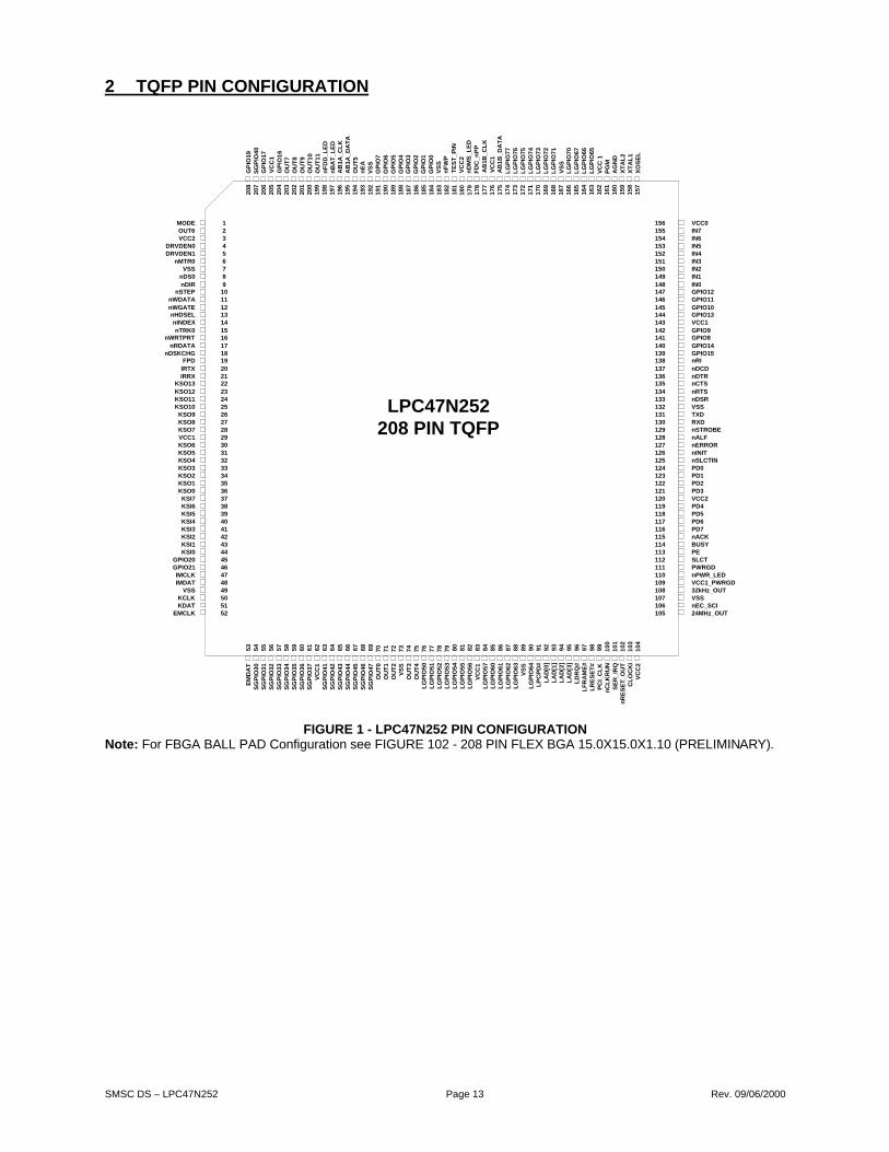
2 TQFP PIN CONFIGURATION
208
207
206
205
204
203
202
201
200
199
198
197
196
195
194
193
192
191
190
189
188
187
186
185
184
183
182
181
180
179
178
177
176
175
174
173
172
171
170
169
168
167
166
165
164
163
162
161
160
159
158
157
123456789
10111213141516171819202122232425262728293031323334353637383940414243444546474849505152
53
54
55
56
57
58
59
60
61
62
63
64
65
66
67
68
69
70
71
72
73
74
75
76
77
78
79 80
81
82
83
84
85
86
87
88
89
90
91
92
93
94
95
96
97
98
99
100
101
102
103
104
156155154153152151150149148147146145144143142141140139138137136135134133132131130129128127126125124123122121120119118117116115114113112111110109108107106105
GP
IO19
SG
PIO
40
GP
IO17
VC
C1
GP
IO16
OU
T7
OU
T8
OU
T9
OU
T10
OU
T11
nF
DD
_L
ED
nB
AT
_L
ED
AB
1A
_C
LK
AB
1A
_D
AT
AO
UT
5n
EA
VS
SG
PIO
7G
PIO
6G
PIO
5G
PIO
4G
PIO
3G
PIO
2G
PIO
1G
PIO
0V
SS
nF
WP
TE
ST
_P
INV
CC
2n
DM
S_L
ED
FD
C_n
PP
AB
1B
_C
LK
VC
C1
AB
1B
_D
AT
AL
GP
IO77
LG
PIO
76
LG
PIO
75
LG
PIO
74
LG
PIO
73
LG
PIO
72
LG
PIO
71
VS
SL
GP
IO70
LG
PIO
67
LG
PIO
66
LG
PIO
65
VC
C 1
PG
MA
GN
DX
TA
L2
XT
AL
1X
OS
EL
MODEOUT6VCC2
DRVDEN0DRVDEN1
nMTR0VSS
nDS0nDIR
nSTEPnWDATAnWGATEnHDSELnINDEXnTRK0
nWRTPRTnRDATA
nDSKCHGFPD
IRTXIRRX
KSO13KSO12KSO11KSO10
KSO9KSO8KSO7VCC1KSO6KSO5KSO4KSO3KSO2KSO1KSO0KSI7KSI6KSI5KSI4KSI3KSI2KSI1KSI0
GPIO20GPIO21IMCLKIMDAT
VSSKCLKKDAT
EMCLK
EM
DA
TS
GP
IO30
SG
PIO
31
SG
PIO
32
SG
PIO
33
SG
PIO
34
SG
PIO
35
SG
PIO
36
SG
PIO
37
VC
C1
SG
PIO
41
SG
PIO
42
SG
PIO
43
SG
PIO
44
SG
PIO
45
SG
PIO
46
SG
PIO
47
OU
T0
OU
T1
OU
T2
VS
SO
UT
3O
UT
4L
GP
IO50
LG
PIO
51
LG
PIO
52
LG
PIO
53
LG
PIO
54
LG
PIO
55
LG
PIO
56
VC
C1
LG
PIO
57
LG
PIO
60
LG
PIO
61
LG
PIO
62
LG
PIO
63
VS
SL
GP
IO64
LP
CP
D#
LA
D[0
]L
AD
[1]
LA
D[2
]L
AD
[3]
LD
RQ
#L
FR
AM
E#
LR
ES
ET
#P
CI_
CL
Kn
CL
KR
UN
SE
R_IR
Qn
RE
SE
T_O
UT
CL
OC
KI
VC
C2
VCC0IN7IN6IN5IN4IN3IN2IN1IN0GPIO12GPIO11GPIO10GPIO13VCC1GPIO9GPIO8GPIO14GPIO15nRInDCDnDTRnCTSnRTSnDSRVSSTXDRXDnSTROBEnALFnERRORnINITnSLCTINPD0PD1PD2PD3VCC2PD4PD5PD6PD7nACKBUSYPESLCTPWRGDnPWR_LEDVCC1_PWRGD32kHz_OUTVSSnEC_SCI24MHz_OUT
LPC47N252208 PIN TQFP
FIGURE 1 - LPC47N252 PIN CONFIGURATIONNote: For FBGA BALL PAD Configuration see FIGURE 102 - 208 PIN FLEX BGA 15.0X15.0X1.10 ( PR ELIMIN AR Y) .

SMSC DS – LPC47N252 Page 14 Rev. 09/06/2000
AB1A_DATA, AB1A_CLK
AB2A_DATA *, AB2A_CLK *
PWM0*, PWM1*, PWM2*
KCLK, EMCLK, IMCLK, PS2CLK*
KSI[0:7]
KS0[0:13], KS0[14:15]*
nBAT_LED, nPWR_LED, nFDD_LED
IN0-7
OUT0-11
GPIO 16-21
GPIO 0-15
nSLCTIN, nINIT, nALF, nSTROBE
BUSY, SLCT, PE, nERROR, nACK
PD[0:7]
IRRX2
IRTX*
IRRX*
TXD, nRTS, nDTR
RXD, nCTS, nDSR, nDCD
nRI
IRTX2
IRMODE / IRRX3A, IRMODE /IRRX3B
KDAT, EMDAT, IMDAT, PS2DAT*
SGPIO 30-37, 40-47
LGPIO 50-57, 60-67, 70-77, IRRX*, IRTX*
VCC1(3)VCC2(4)
VSS(9)
RTC2 x 128 BYTEBANKS OFCMOS RAM
BANK1
SYSTEMRESET
CONTROLINPUTS
PLL CLOCKGENERATOR
BANK2
WDT
CONFIGURATION REGISTERSPOWER
MANAGEMENT
8051
RingOscillator
w/ FAIL SAFE
256B DirectRAM
MAILBOXREGISTERS
8051SUB-BLOCKEXTERNALCONTROL
REGISTERS
256BEXTERNAL8051 RAM
LEDDRIVER
GENERAL PURPOSE I/O INTERFACE
OUT
IN
I/O
I/O
16 x 8KEYBOARDINTERFACE
16C550COMPATIBLE
SERIAL PORT 1
INFRARED
MULTI-MODEPARALLELPORT / FDC
MUX
PS/2PORTS
ACCESSBUS
ACCESSBUS2
PWMFan
Control
CONTROL, ADDRESS, DATA
* -- ALTERNATE FUNCTION
VCC2 POWERED
VCC1 POWERED
nRESET_OUT
LAD [3:0]nLDRQ
nLPCPDnLFRAMEnLRESET
nIRQ8*
MODEnEA
24MHz_OUT
PWRGD
32KHz_OUT
VCC1_PWRGD
CLOCKI(14.318 MHz)
XOSEL
XTAL2
XTAL1VCC0
AGND
nDSKCHG,nWRTPRT,nTRK0, nINDEX
nWGATE, nHDSEL, nDIR,nSTEP, nDS0, nDS1*, nMTR0,nMTR1*, DRVDEN0, DRVDEN1,FPD
DIGITAL DATASEPARATORWITH WRITE
PRECOMPENSATION
SMSCPROPRIETARY
82077 COMPATIBLEVERTICAL FLOPPY DISK
CONTROLLER CORE
MD
AT
A
MC
LOC
K
RD
AT
A
RC
LOC
K
nWDATA
nRDATA
ACPIEMBEDDED
CONTROLLER
INTERRUPTSSER_IRQ
PCI_CLKnCLKRUN
nEC_SCI
nSMI*
PM1BLOCK
LPC BUSHOST CPUINTERFACE
nEC_SCI
I/O
I/O
FAN_TACH1*, FAN_TACH2*
AB2B_DATA *, AB2B_CLK *
AB1B_DATA, AB1B_CLK
64KFLASH ROM
KBRST*, A20M*
8051TX*
8051RX*
FIGURE 2 – LPC47N252 BLOCK DIAGRAM
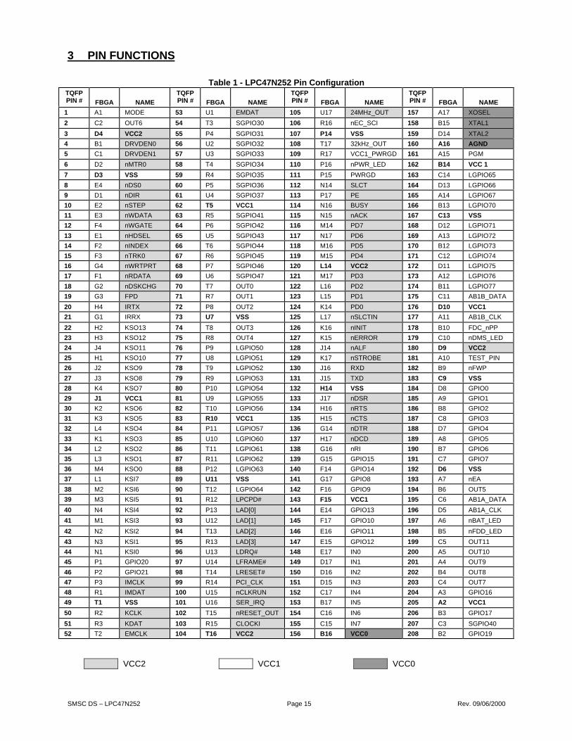
SMSC DS – LPC47N252 Page 15 Rev. 09/06/2000
3 PIN FUNCTIONS
Table 1 - LPC47N252 Pin ConfigurationTQFPPIN # FBGA NAME
TQFPPIN # FBGA NAME
TQFPPIN # FBGA NAME
TQFPPIN # FBGA NAME
1 A1 MODE 53 U1 EMDAT 105 U17 24MHz_OUT 157 A17 XOSEL
2 C2 OUT6 54 T3 SGPIO30 106 R16 nEC_SCI 158 B15 XTAL1
3 D4 VCC2 55 P4 SGPIO31 107 P14 VSS 159 D14 XTAL2
4 B1 DRVDEN0 56 U2 SGPIO32 108 T17 32kHz_OUT 160 A16 AGND
5 C1 DRVDEN1 57 U3 SGPIO33 109 R17 VCC1_PWRGD 161 A15 PGM
6 D2 nMTR0 58 T4 SGPIO34 110 P16 nPWR_LED 162 B14 VCC 1
7 D3 VSS 59 R4 SGPIO35 111 P15 PWRGD 163 C14 LGPIO65
8 E4 nDS0 60 P5 SGPIO36 112 N14 SLCT 164 D13 LGPIO66
9 D1 nDIR 61 U4 SGPIO37 113 P17 PE 165 A14 LGPIO67
10 E2 nSTEP 62 T5 VCC1 114 N16 BUSY 166 B13 LGPIO70
11 E3 nWDATA 63 R5 SGPIO41 115 N15 nACK 167 C13 VSS
12 F4 nWGATE 64 P6 SGPIO42 116 M14 PD7 168 D12 LGPIO71
13 E1 nHDSEL 65 U5 SGPIO43 117 N17 PD6 169 A13 LGPIO72
14 F2 nINDEX 66 T6 SGPIO44 118 M16 PD5 170 B12 LGPIO73
15 F3 nTRK0 67 R6 SGPIO45 119 M15 PD4 171 C12 LGPIO74
16 G4 nWRTPRT 68 P7 SGPIO46 120 L14 VCC2 172 D11 LGPIO75
17 F1 nRDATA 69 U6 SGPIO47 121 M17 PD3 173 A12 LGPIO76
18 G2 nDSKCHG 70 T7 OUT0 122 L16 PD2 174 B11 LGPIO77
19 G3 FPD 71 R7 OUT1 123 L15 PD1 175 C11 AB1B_DATA
20 H4 IRTX 72 P8 OUT2 124 K14 PD0 176 D10 VCC1
21 G1 IRRX 73 U7 VSS 125 L17 nSLCTIN 177 A11 AB1B_CLK
22 H2 KSO13 74 T8 OUT3 126 K16 nINIT 178 B10 FDC_nPP
23 H3 KSO12 75 R8 OUT4 127 K15 nERROR 179 C10 nDMS_LED
24 J4 KSO11 76 P9 LGPIO50 128 J14 nALF 180 D9 VCC2
25 H1 KSO10 77 U8 LGPIO51 129 K17 nSTROBE 181 A10 TEST_PIN
26 J2 KSO9 78 T9 LGPIO52 130 J16 RXD 182 B9 nFWP
27 J3 KSO8 79 R9 LGPIO53 131 J15 TXD 183 C9 VSS
28 K4 KSO7 80 P10 LGPIO54 132 H14 VSS 184 D8 GPIO0
29 J1 VCC1 81 U9 LGPIO55 133 J17 nDSR 185 A9 GPIO1
30 K2 KSO6 82 T10 LGPIO56 134 H16 nRTS 186 B8 GPIO2
31 K3 KSO5 83 R10 VCC1 135 H15 nCTS 187 C8 GPIO3
32 L4 KSO4 84 P11 LGPIO57 136 G14 nDTR 188 D7 GPIO4
33 K1 KSO3 85 U10 LGPIO60 137 H17 nDCD 189 A8 GPIO5
34 L2 KSO2 86 T11 LGPIO61 138 G16 nRI 190 B7 GPIO6
35 L3 KSO1 87 R11 LGPIO62 139 G15 GPIO15 191 C7 GPIO7
36 M4 KSO0 88 P12 LGPIO63 140 F14 GPIO14 192 D6 VSS
37 L1 KSI7 89 U11 VSS 141 G17 GPIO8 193 A7 nEA
38 M2 KSI6 90 T12 LGPIO64 142 F16 GPIO9 194 B6 OUT5
39 M3 KSI5 91 R12 LPCPD# 143 F15 VCC1 195 C6 AB1A_DATA
40 N4 KSI4 92 P13 LAD[0] 144 E14 GPIO13 196 D5 AB1A_CLK
41 M1 KSI3 93 U12 LAD[1] 145 F17 GPIO10 197 A6 nBAT_LED
42 N2 KSI2 94 T13 LAD[2] 146 E16 GPIO11 198 B5 nFDD_LED
43 N3 KSI1 95 R13 LAD[3] 147 E15 GPIO12 199 C5 OUT11
44 N1 KSI0 96 U13 LDRQ# 148 E17 IN0 200 A5 OUT10
45 P1 GPIO20 97 U14 LFRAME# 149 D17 IN1 201 A4 OUT9
46 P2 GPIO21 98 T14 LRESET# 150 D16 IN2 202 B4 OUT8
47 P3 IMCLK 99 R14 PCI_CLK 151 D15 IN3 203 C4 OUT7
48 R1 IMDAT 100 U15 nCLKRUN 152 C17 IN4 204 A3 GPIO16
49 T1 VSS 101 U16 SER_IRQ 153 B17 IN5 205 A2 VCC1
50 R2 KCLK 102 T15 nRESET_OUT 154 C16 IN6 206 B3 GPIO17
51 R3 KDAT 103 R15 CLOCKI 155 C15 IN7 207 C3 SGPIO40
52 T2 EMCLK 104 T16 VCC2 156 B16 VCC0 208 B2 GPIO19
VCC2 VCC1 VCC0
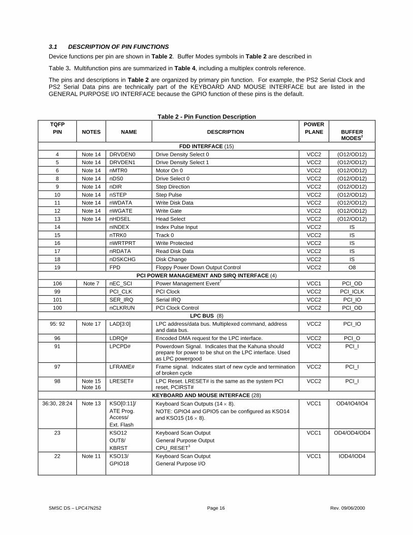
SMSC DS – LPC47N252 Page 16 Rev. 09/06/2000
3.1 DESCRIPTION OF PIN FUNCTIONS
Device functions per pin are shown in Table 2. Buffer Modes symbols in Table 2 are described in
Table 3. Multifunction pins are summarized in Table 4, including a multiplex controls reference.
The pins and descriptions in Table 2 are organized by primary pin function. For example, the PS2 Serial Clock andPS2 Serial Data pins are technically part of the KEYBOARD AND MOUSE INTERFACE but are listed in theGENERAL PURPOSE I/O INTERFACE because the GPIO function of these pins is the default.
Table 2 - Pin Function DescriptionTQFP
PIN NOTES NAME DESCRIPTION
POWER
PLANE BUFFERMODES2
FDD INTERFACE (15)
4 Note 14 DRVDEN0 Drive Density Select 0 VCC2 (O12/OD12)
5 Note 14 DRVDEN1 Drive Density Select 1 VCC2 (O12/OD12)
6 Note 14 nMTR0 Motor On 0 VCC2 (O12/OD12)
8 Note 14 nDS0 Drive Select 0 VCC2 (O12/OD12)
9 Note 14 nDIR Step Direction VCC2 (O12/OD12)
10 Note 14 nSTEP Step Pulse VCC2 (O12/OD12)
11 Note 14 nWDATA Write Disk Data VCC2 (O12/OD12)
12 Note 14 nWGATE Write Gate VCC2 (O12/OD12)
13 Note 14 nHDSEL Head Select VCC2 (O12/OD12)
14 nINDEX Index Pulse Input VCC2 IS
15 nTRK0 Track 0 VCC2 IS
16 nWRTPRT Write Protected VCC2 IS
17 nRDATA Read Disk Data VCC2 IS
18 nDSKCHG Disk Change VCC2 IS
19 FPD Floppy Power Down Output Control VCC2 O8
PCI POWER MANAGEMENT AND SIRQ INTERFACE (4)
106 Note 7 nEC_SCI Power Management Event7 VCC1 PCI_OD
99 PCI_CLK PCI Clock VCC2 PCI_ICLK
101 SER_IRQ Serial IRQ VCC2 PCI_IO
100 nCLKRUN PCI Clock Control VCC2 PCI_OD
LPC BUS (8)
95: 92 Note 17 LAD[3:0] LPC address/data bus. Multiplexed command, addressand data bus.
VCC2 PCI_IO
96 LDRQ# Encoded DMA request for the LPC interface. VCC2 PCI_O
91 LPCPD# Powerdown Signal. Indicates that the Kahuna shouldprepare for power to be shut on the LPC interface. Usedas LPC powergood
VCC2 PCI_I
97 LFRAME# Frame signal. Indicates start of new cycle and terminationof broken cycle
VCC2 PCI_I
98 Note 15Note 16
LRESET# LPC Reset. LRESET# is the same as the system PCIreset, PCIRST#
VCC2 PCI_I
KEYBOARD AND MOUSE INTERFACE (28)
36:30, 28:24 Note 13 KSO[0:11]/
ATE Prog.Access/Ext. Flash
Keyboard Scan Outputs (14 × 8).
NOTE: GPIO4 and GPIO5 can be configured as KSO14and KSO15 (16 × 8).
VCC1 OD4/IO4/IO4
23 KSO12
OUT8/
KBRST
Keyboard Scan Output
General Purpose Output
CPU_RESET3
VCC1 OD4/OD4/OD4
22 Note 11 KSO13/GPIO18
Keyboard Scan OutputGeneral Purpose I/O
VCC1 IOD4/IOD4

SMSC DS – LPC47N252 Page 17 Rev. 09/06/2000
TQFP
PIN NOTES NAME DESCRIPTION
POWER
PLANE BUFFERMODES2
44:38 Note 13 KSI[0:6] ]/ATE Prog.Access/
Ext. Flash
Keyboard Scan Inputs VCC1 ISP/IO4/IO4
37 KSI7 Keyboard Scan Inputs VCC1 ISP
52 EMCLK EM Serial Clock VCC2 IOD16
53 EMDAT EM Serial Data VCC2 IOD16
47 IMCLK IM Serial Clock VCC2 IOD16
48 IMDAT IM Serial Data VCC2 IOD16
51 KDAT Keyboard Data VCC2 IOD16
50 KCLK Keyboard Clock VCC2 IOD16
GENERAL PURPOSE I/O INTERFACE (81)
70 Note 7,Note 8
OUT0 (SCI) General Purpose Output (SCI) VCC1 (O12/OD12)
71 Note 3 OUT1/
nIRQ8
General Purpose Output/
Active Low RTC IRQ3
VCC1 O12/O12
72 OUT2 General Purpose Output VCC1 O12
74 OUT3 General Purpose Output VCC1 O12
75 OUT4 General Purpose Output VCC1 O12
194 Note 3 OUT5/
nDS1/KBRST
General Purpose Output
FDD Drive Select 13
CPU_RESET3
VCC1 O12/(O12/OD12)/O12
2 Note 3 OUT6/
nMTR1
General Purpose Output
FDD Motor On 13
VCC1 O12/(O12/OD12)
203 Note 3 OUT7/nSMI
General Purpose OutputSMI Output3
VCC1 O12/OD12
202 Note 3 OUT8/
KBRST
General Purpose Output
CPU_RESET
VCC1 O12/O12
201 Note 3 OUT9/
PWM2
General Purpose Output
Pulse Width Modulator Output
VCC1 O12/O12
200 OUT10/
PWM0
General Purpose Output
Pulse Width Modulator Output
VCC1 O12/O12
199 OUT11/
PWM1
General Purpose Output
Pulse Width Modulator Output
VCC1 O12/O12
148 Note 4 IN0 (WK_EE4) General Purpose Input VCC1 I
149 Note 4 IN1 (WK_EE2) General Purpose Input VCC1 I
150 Note 4 IN2 (WK_EE3) General Purpose Input VCC1 I
151 IN3(nGPWKUP)
General Purpose Input (General Purpose Wake Up) VCC1 I
152 Note 5 IN4 (WK_SE00) General Purpose Input VCC1 I
153 Note 5 IN5 (WK_SE01) General Purpose Input VCC1 I
154 Note 5 IN6 (WK_SE05) General Purpose Input VCC1 I
155 Note 4 IN7 (WK_EE1) General Purpose Input VCC1 I
184 Note 5 GPIO0(WK_SE02)
General Purpose I/O VCC1 IO8
185 Note 5 GPIO1(WK_SE03)
General Purpose I/O VCC1 IO8
186 Note 5 GPIO2(WK_SE04)
General Purpose I/O VCC1 IO8
187 Note 6 GPIO3(TRIGGER)
General Purpose I/O (Interrupt 1 Event) VCC1 IO8
188 Note 5 GPIO4(WK_SE07)
KSO14
General Purpose I/O
Keyboard Scan Output
VCC1 IO8/OD8

SMSC DS – LPC47N252 Page 18 Rev. 09/06/2000
TQFP
PIN NOTES NAME DESCRIPTION
POWER
PLANE BUFFERMODES2
189 Note 5 GPIO5(WK_SE10)/
KSO15
General Purpose I/OKeyboard Scan Output
VCC1 IO8/OD8
190 Note 5 GPIO6(WK_SE11)/
IRMODE/IRRX3A
General Purpose I/O
FIR Mode Output or 2nd Receive Input
VCC1 IO8/(O8/I)
191 Note 5,Note 8
GPIO7(WK_SE06)
General Purpose I/O VCC1 (IO8/IOD8)8
141 Note 5 GPIO8(WK_SE12)/IRRX2
General Purpose I/O
IR Receive Input
VCC1 IO8/I
142 Note 1,Note 5
GPIO9(WK_SE13)/
IRTX2
General Purpose I/O
IR Transmit Output
VCC1 IO12/O12
145 Note 5 GPIO10(WK_SE14)/
IRMODE/IRRX3B
General Purpose I/OFIR Mode Output or 2nd Receive Input
VCC1 IO8/O8/(O8/I)
146 Note 5 GPIO11(WK_SE15)/AB2A_DATA
General Purpose I/O
ACCESS.Bus 2 Serial Data (switch position A)
VCC1 IO12 /IOD12
147 Note 5 GPIO12(WK_SE16)AB2A_CLK
General Purpose I/O
ACCESS.Bus 2 Clock (switch position A)
VCC1 IO12 /IOD12
144 Note 5 GPIO13(WK_SE17)
AB2B_DATA
General Purpose I/O
ACCESS.Bus 2 Serial Data (switch position B)
VCC1 IO12 /IOD12
140 Note 5 GPIO14(WK_SE20)
AB2B_CLK
General Purpose I/OACCESS.Bus 2 Clock (switch position B)
VCC1 IO12 /IOD12
139 Note 5 GPIO15(WK_SE21)
FAN_TACH1
General Purpose I/O
Fan Tachometer Input 1
VCC1 IO8/I
204 Note 5 GPIO16(WK_SE22)
FAN_TACH2
General Purpose I/O
Fan Tachometer Input 2
VCC1 IO8/I
206 Note 3,Note 5
GPIO17(WK_SE23)/A20M
General Purpose I/O
KBD GATEA20 Output3
VCC1 IO8/O8
208 Note 5 GPIO19(WK_SE24)
General Purpose I/O VCC1 IO8
45 Note 3,Note 5
GPIO20(WK_SE25)5/PS2CLK/
8051RX/
General Purpose I/O
PS2 Serial Clock3
8051 RX Input
VCC1 IOD16/IOD16/I
46 Note 3,Note 5
GPIO21(WK_SE26)5/
PS2DAT/8051TX
General Purpose I/O
PS2 Serial Data3
8051 TX Input
VCC1 IOD16/IOD16/OD16
54:61 SGPIO30 –SGPIO37
8051 SFR bit-wise addressable GPIO VCC1 IO8/(O8/I)
207, 63:69 SGPIO40 –SGPIO47
8051 SFR bit-wise addressable GPIO VCC1 IO8/(O8/I)
76:84 LGPIO50 –LGPIO57
LPC General Purpose I/O VCC1 IO8
85:90163:165
LGPIO60 –LGPIO67
LPC General Purpose I/O VCC1 IO8

SMSC DS – LPC47N252 Page 19 Rev. 09/06/2000
TQFP
PIN NOTES NAME DESCRIPTION
POWER
PLANE BUFFERMODES2
166,168:174
LGPIO70 –LGPIO77
LPC General Purpose I/O VCC1 IO8
INFRARED INTERFACE (2)
21 IRRX IR Receive Input VCC1 I
20 Note 1 IRTX IR Transmit Output VCC2 O12
PARALLEL PORT INTERFACE (17)
126 nINIT/
nDIR
I nitia te O u tp ut
F DC Dire ct ion Co nt ro l
VCC2 ( OD14 / OP14 ) / O D1 4
125 nSLCTIN/
nSTEP
Print e r Se lect Inp ut
F DC St ep Pu lse
VCC2 ( OD14 / OP14 ) / O D1 4
124 PD0/nINDEX
Por t Dat a 0F DC I n de x
VCC2 I OP14 / I
123 PD1/
nTRK0
Por t Dat a 1
F DC T r ack 0
VCC2 I OP14 / I
122 PD2/
nWRTPRT
Por t Dat a 2
F DC Wr it e Pro te cte d
VCC2 I OP14 / I
121 PD3/
nRDATA
Por t Dat a 3
F DC Re ad Disk Da ta
VCC2 I OP14 / I
119 PD4/
nDSKCHG
Por t Dat a 4
F DC Disk Ch an ge
VCC2 I OP14 / I
118 PD5 Por t Dat a 5 VCC2 I OP14
117 PD6/
nMTR0
Por t Dat a 6
F DC M o to r On 0
VCC2 I OP14 / OD14
116 PD7 Por t Dat a 7 VCC2 I OP14
112 SLCT/
nWGATE
Print e r Se lecte d Sta t us
F DC Wr it e Gat e
VCC2 I /O D1 2
113 PE/
nWDATA
Pap er En d
F DC Wr it e Dat a
VCC2 I /O D1 2
114 BUSY/
nMTR1
Busy
F DC M o to r On 1
VCC2 I /O D1 2
115 nACK/
nDS1
Ackno wle dg e
F DC Dr ive Select 1
VCC2 I /O D1 2
127 nERROR/
nHDSEL
Err or
F DC He ad Se le ct
VCC2 I /O D1 2
128 nALF/DRVDEN0
Aut of e ed O u tp ut F DC De nsit y Sele ct 0
VCC2 ( OD14 / OP14 ) /O D14
129 nSTROBE/
nDS0
Str ob e O ut p ut
F DC Dr ive Select 0
VCC2 ( OD14 / OP14 ) /O D14
SERIAL PORT INTERFACE (8)
130 RXD Receive Data VCC2 I
131 TXD Transmit Data VCC2 O12
133 nDSR Data Set Ready VCC2 I
134 nRTS Request to Send VCC2 O8
135 nCTS Clear to Send VCC2 I
136 nDTR Data Terminal Ready VCC2 O8
138 nRI Ring Indicator VCC1 I
137 nDCD Data Carrier Detect VCC2 I
MISCELLANEOUS (17)
108 32kHz_OUT 32.768kHz Output Clock VCC1 O8
105 24MHz_OUT 24MHz Clock Output VCC2 O24
103 CLOCKI 14.318MHz Clock Input VCC2 ICLK
1 Note 18 MODE Configuration Ports Base Address Select VCC1 I
157 Note 10 XOSEL10 External 32kHz Clock Enable Input VCC0 I
109 Note 9 VCC1_PWRGD VCC1 Power Good Input VCC1 I

SMSC DS – LPC47N252 Page 20 Rev. 09/06/2000
TQFP
PIN NOTES NAME DESCRIPTION
POWER
PLANE BUFFERMODES2
102 nRESET_OUT System Reset VCC2 O8
197 nBAT_LED Battery LED (0 = ON) VCC1 OD12
110 nPWR_LED Power LED (0 = ON) VCC1 OD12
198 nFDD_LED Floppy LED (0 = ON) VCC1 OD12
179 nDMS_LED Dead Man Switch LED (0 = ON). (See section 13.9) VCC1 OD12
111 Note 9 PWRGD VCC2 Power Good Input VCC1 I
161 Note 12 PGM Flash Programming Enable
(see section 13.6, ATE Flash Program Access)
VCC1 IPD
182 nFWP Flash Boot Block Write Protect (see section 12.4, FlashBoot Block Protect Controls)
VCC1 I
178 FDC_nPP FDC on Parallel Port Detect Pin VCC1 I
193 nEA Internal/External Flash Select (spec section 13.7, ExternalFlash Interface)
VCC1 I
181 TEST_PIN No Connect. This pin provides acess to the SMSC boardlevel XNOR-Chain test.
See Section 30 on page 289.
VCC1 -
ACCESS BUS INTERFACE (4)
195 AB1A_DATA ACCESS.Bus 1 Serial Data (switch position A) VCC1 IOD12
196 AB1A_CLK ACCESS.Bus 1 Clock (switch position A) VCC1 IOD12
175 AB1B_DATA ACCESS.Bus 1 Serial Data (switch position B) VCC1 IOD12
177 AB1B_CLK ACCESS.Bus 1 Clock (switch position B) VCC1 IOD12
REAL TIME CLOCK INTERFACE (2)
158 XTAL1 32.768kHz Crystal Input VCC0 ICLK2
159 Note 10 XTAL210 32.768kHz Crystal Output VCC0 (OCLK2/I)
POWER PLANES (22)
156 VCC0 RTC (VBAT) Supply Voltage (×1)
29, 62, 83,143, 162,
176
VCC1 +3.3V ± 5% Main Battery Supply (×7)
3, 104, 120,180
VCC2 +3.3V ± 5% Switched AC/Main Battery Supply (×4)
160 AGND Analog Ground (×1)
7, 49, 73,89, 107,132, 167,183, 192,
VSS Digital Ground (×9)
Note 1: These pins default to “output”, “low” to prevent infrared transceiver damage.
Note 2: Buffer Modes per function on multiplexed pins are separated by a slash “/”; e.g., a pin with two multiplexedfunctions where the primary function is an input and the secondary function is an 8mA bi-directional driver isrepresented as “I/IO8”. Buffer Modes in parenthesis represent multiple buffer modes for a single pin function.
Note 3: This pin is tristated when PWRGD is inactive and the pin is configured as a VCC2-powered alternatefunction.
Note 4: These devices can generate wake-up events on either edge of the signal that is applied when the pin isconfigured as an input. The interrupts are masked by the Wake-up Mask Register bits.
Note 5: These devices can generate wake-up events on selectable edges of the signal that is applied when the pinis configured as an input. The interrupts are masked by the Wake-up Mask Registers and selected edges areprogrammed via the Edge Select registers (see Tikki section 8051 Internal Parallel Interrupts on page 151).
Note 6: This interrupt is masked by INT1 Mask Register bit 3. GPIO3 is the only GPIO pin which does not generatea wakeup event.
Note 7: The nEC_SCI pin can be controlled by hardware and 8051 software. The nEC_SCI pin can drive either theACPI Run-time GPE Chipset input or the Wake GPE Chipset input (FIGURE 8 on page 75). Depending how thenEC_SCI pin is used, other ACPI-related SCI functions may be best supplied by LPC47N252 general purpose outputOUT0.

SMSC DS – LPC47N252 Page 21 Rev. 09/06/2000
Note 8: OUT0 and GPIO7 are suitable as an SCI output pin because the buffer type can be configured as a push-pull * or open-drain output (see section 24.4.3.5.)
Note 9: Input levels for the PWRGD and VCC1_PWRGD pins are as follows: VIL = VSS ±400mV and VIH = VCC1
±400mV. VCC1_PWRGD must be driven high or low at all times. VCC1_PWRGD may be tied high but VCC0 mustbe connected to VCC1 and all RTC time-keeping and CMOS memory functions are invalidated.
Note 10:The function of these pins are described in the 32kHz Clock Input section 27.10.
Note 11: The GPIO18 alternate function of the KS013 pin has no wake-up capability (see note following Figure 21 onpage 152 in Tikki)
Note 12:This pin has an internal pull-down resistor to guarantee that the input remains deasserted whenunconnected. This input must also be easily pulled-up by ATE.
Note 13:These pins are multiplexed according to the PGM and nEA pins to support an external Flash interface and tosupport internal Flash programming (see spec sections section 13.2 Flash Program Interface Decoder, 13.6 ATEFlash Program Access and section 13.7, External Flash Interface, and 13.8 Keyboard Controller Bus MonitorInterface).Note 14: The FDC output pins can be configured as either Open Drain outputs capable of sinking 12mA(OD12) or as push-pull outputs capable of driving 6mA and sinking 12mA (O12). The FDC output pins must tristatewhen the FDC is in powerdown mode (The board designer must provide external pull-up resistors on these outputpins).
Note 15: LPCPD# is a VCC2-powered signal but is sensed by the 8051 on VCC1 (see section 11.8.3.6).
Note 16: In the LPC47N252, Hard Reset is generated internally by the 8051 for all SIO blocks except for the LPCHost Interface where LRESET#, alone, provides this function..
Note 17: These pins require a weak pull-up resistors of 10k-100k ohms.
Note 18: The input path for the MODE pin pad has a Vt drop when passing a logic high signal.
Table 3 - Buffer Mode
BUFFER SYMBOL DESCRIPTION
I Input
IO12 Bidirectional – 12mA sink, 6mAsource
IO4 Bidirectional – 4mA, 2mA source
IO8 Bidirectional – 8mA, 4mA source
IOD16 Input, open drain output – 16mA sink
IOD8 Input, open drain output – 8mA sink
IOP14 Bidirectional – 14mA sink, 14mAsource, backdrive protected
IP Input with pullup
IPD Input with pullup
IS Schmitt trigger input
ISP Schmitt trigger input with pullup
O12 Output – 12mA, 6mA source
O8 Output – 8mA, 4mA source
OD12 Open drain – 12mA sink
OD14 Open drain – 14mA sink
OD16 Open drain – 16mA sink
OD4 Open drain – 4mA sink
OD8 Open drain – 8mA sink
OP14 Output – 14mA sink, 14mA source,backdrive protected
PCI_I PCI input

SMSC DS – LPC47N252 Page 22 Rev. 09/06/2000
BUFFER SYMBOL DESCRIPTION
PCI_ICLK PCI clock input
PCI_IO PCI bidirectional
PCI_O PCI ouput
PCI_OD PCI open drain
ICLK Clock input
ICLK2 Clock input 2
OCLK2 Clock output 2
O24 Output – 12mA, 6mA source
3.1.1 ALTERNATE FUNCTION PINS
Many of the LPC47N252’s signal pins provide alternate functions which may be enabled by the 8051 firmware basedon the system design requirements: The pins are identified by primary pin function (Note that some functions areavailable on more than one pin; e.g., OUT8 and KBRST.
Table 4 - Alternate Function PinsMULTIPLEX CONTROLSDEFAULT
FUNCTION PWR
ALTERNATEFUNCTION #1 PWR
ALTERNATEFUNCTION #2 PWR BIT NOTES
OUT1 VCC1 nIRQ8 VCC2 - - MISC0 Note 20
OUT5 VCC1 nDS1 VCC2 KBRST VCC2 MISC[5, 22] Note 20Note 22
OUT6 VCC1 nMTR1 VCC2 - - MISC5 Note 20
OUT7 VCC1 nSMI VCC2 - - MISC18 Note 20
OUT8 VCC1 KBRST VCC2 MISC[17, 6] Note 20
OUT9 VCC1 PWM2 VCC1 - - MISC11
OUT10 VCC1 PWM0 VCC1 - - MISC4
OUT11 VCC1 PWM1 VCC1 - - MISC12
GPIO4 VCC1 KSO14 VCC1 - -
GPIO5 VCC1 KSO15 VCC1 - -
MISC9
GPIO6 VCC1 IRMODE/IRRX3A VCC2 - - MISC[14, 13] Note 20
GPIO8 VCC1 IRRX2 VCC1 - -
GPIO9 VCC1 IRTX2 VCC2 - -
MISC[7, 2]
Note 21
GPIO10 VCC1 IRMODE/IRRX3B VCC2 - - MISC[16, 15]
GPIO11 VCC1 AB2A_DATA VCC1
GPIO12 VCC1 AB2A_CLK VCC1
GPIO13 VCC1 AB2B_DATA VCC1
GPIO14 VCC1 AB2B_CLK VCC1
MISC[20, 19]
GPIO15 VCC1 FAN_TACH1 VCC1 MISC23 MISC23
GPIO16 VCC1 FAN_TACH2 VCC1 MISC21 MISC21
GPIO17 VCC1 A20M VCC1 - - MISC6 Note 20
GPIO20 VCC1 PS2CLK VCC2 8051RX VCC1 Note 20
GPIO21 VCC1 PS2DAT VCC2 8051TX VCC1
MISC[3, 1]
Note 20
KSO12 VCC1 OUT8 VCC1 KBRST VCC2 MISC[17, 6] Note 20
KSO13 VCC1 GPIO18 VCC1 MISC[17]
nINIT VCC2 nDIR VCC2 - -
nSLCTIN VCC2 nSTEP VCC2 - -
PD0 VCC2 nINDEX VCC2 - -
PD1 VCC2 nTRK0 VCC2 - -
PD2 VCC2 nWRTPRT VCC2 - -
PD3 VCC2 nRDATA VCC2 - -
PD4 VCC2 nDSKCHG VCC2 - -
PD6 VCC2 nMTR0 VCC2 - -
SLCT VCC2 nWGATE VCC2 - -
CR2 5[ 4 :3 ]
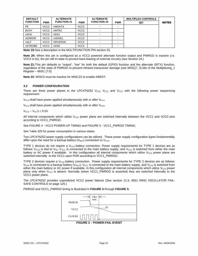
SMSC DS – LPC47N252 Page 23 Rev. 09/06/2000
MULTIPLEX CONTROLSDEFAULTFUNCTION PWR
ALTERNATEFUNCTION #1 PWR
ALTERNATEFUNCTION #2 PWR BIT NOTES
PE VCC2 nWDATA VCC2 - -
BUSY VCC2 nMTR1 VCC2 - -
nACK VCC2 nDS1 VCC2 - -
nERROR VCC2 nHDSEL VCC2 - -
nALF VCC2 DRVDEN0 VCC2 - -
nSTROBE VCC2 nDS0 VCC2 - -
NOTESNOTES
Note 19:See a description in the MULTIFUNCTION PIN section 25.
Note 20: When this pin is configured as a VCC2 powered alternate function output and PWRGD is inactive (i.e.VCC2 is 0v), the pin will tri-state to prevent back-biasing of external circuitry (see Section 24.)
Note 21:This pin defaults to “output”, “low” for both the default (GPIO) function and the alternate (IRTX) function,regardless of the state of PWRGD to prevent infrared transceiver damage (see MISC[7, 2] bits of the Multiplexing_1Register – MISC (7:0)
Note 22: MISC5 must be inactive for MISC22 to enable KBRST.
3.2 POWER CONFIGURATION
There are three power planes in the LPC47N252 VCC0, VCC1, and VCC2 with the following power sequencingrequirement:
VCC2 shall have power applied simultaneously with or after VCC1.
VCC1 shall have power applied simultaneously with or after VCC0.
VCC2 – VCC1 ≤ 0.5V
All internal components which utilize VCC0 power plane are switched internally between the VCC1 and VCC0 pinsaccording to VCC1_PWRGD.
See FIGURE 4 - VCC2 POWER-UP TIMING and FIGURE 5 - VCC1_PWRGD TIMING.
See Table 325 for power consumption in various states.
Two LPC47N252 power supply configurations can be utilized. These power supply configuration types fundamentallydiffer upon the need for a backup battery (VBAT) connection to VCC0.
TYPE 1 devices do not require a VCC0 battery connection. Power supply requirements for TYPE 1 devices are asfollows: VCC0 is tied to VSS, VCC1 is connected to the main battery supply, and VCC2 is switched from either the mainbattery or AC power if available. In this configuration all internal components which utilize VCC0 power plane areswitched internally to the VCC1 upon POR according to VCC1_PWRGD.
TYPE 2 devices require a VCC0 battery connection. Power supply requirements for TYPE 2 devices are as follows:VCC0 is connected to a backup battery (VBAT), VCC1 is connected to the main battery supply, and VCC2 is switched fromeither the main battery or AC power if available. In this configuration all internal components which utilize VCC0 powerplane only when VCC1 is absent. Normally (when VCC1_PWRGD is asserted) they are switched internally to theVCC1 power plane.
The LPC47N252 provides unpredicted VCC2 power failures (See section 11.6, 8051 RING OSCILLATOR FAIL-SAFE CONTROLS on page 125.)
PWRGD and VCC1_PWRGD timing is illustrated in FIGURE 3 through FIGURE 5.
PWRGD
VCC2
CLOCKI
10µs
3V
min.
FIGURE 3 – POWER-FAIL EVENT

SMSC DS – LPC47N252 Page 24 Rev. 09/06/2000
PWRGD
VCC23V
CLOCKI
10µsmin.
FIGURE 4 - VCC2 POWER-UP TIMING
VCC1_PWRGD
VCC13V 3V
1µsmin.
1µsmin.
FIGURE 5 - VCC1_PWRGD TIMING
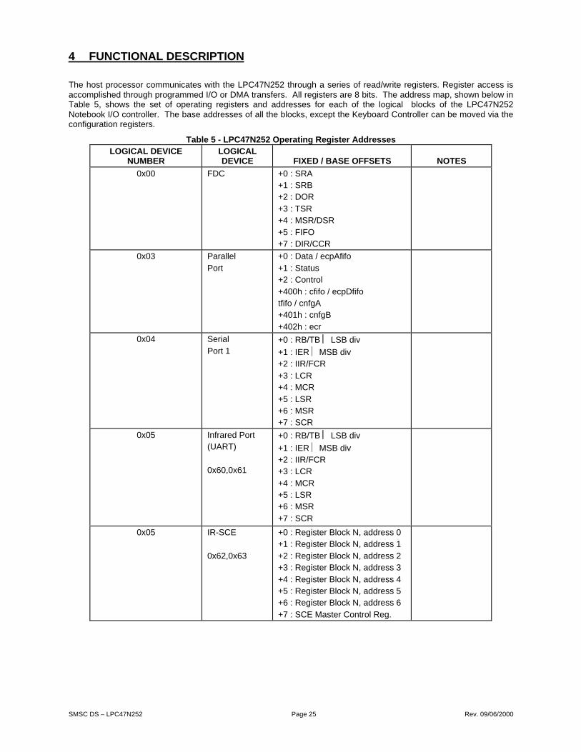
SMSC DS – LPC47N252 Page 25 Rev. 09/06/2000
4 FUNCTIONAL DESCRIPTION
The host processor communicates with the LPC47N252 through a series of read/write registers. Register access isaccomplished through programmed I/O or DMA transfers. All registers are 8 bits. The address map, shown below inTable 5, shows the set of operating registers and addresses for each of the logical blocks of the LPC47N252Notebook I/O controller. The base addresses of all the blocks, except the Keyboard Controller can be moved via theconfiguration registers.
Table 5 - LPC47N252 Operating Register AddressesLOGICAL DEVICE
NUMBERLOGICALDEVICE FIXED / BASE OFFSETS NOTES
0x00 FDC +0 : SRA+1 : SRB+2 : DOR
+3 : TSR+4 : MSR/DSR
+5 : FIFO+7 : DIR/CCR
0x03 Parallel
Port
+0 : Data / ecpAfifo
+1 : Status+2 : Control
+400h : cfifo / ecpDfifotfifo / cnfgA+401h : cnfgB
+402h : ecr
0x04 Serial
Port 1+0 : RB/TB LSB div
+1 : IER MSB div+2 : IIR/FCR
+3 : LCR+4 : MCR
+5 : LSR+6 : MSR+7 : SCR
0x05 Infrared Port(UART)
0x60,0x61
+0 : RB/TB LSB div
+1 : IER MSB div+2 : IIR/FCR+3 : LCR
+4 : MCR+5 : LSR+6 : MSR
+7 : SCR
0x05 IR-SCE
0x62,0x63
+0 : Register Block N, address 0+1 : Register Block N, address 1
+2 : Register Block N, address 2+3 : Register Block N, address 3
+4 : Register Block N, address 4+5 : Register Block N, address 5+6 : Register Block N, address 6
+7 : SCE Master Control Reg.

SMSC DS – LPC47N252 Page 26 Rev. 09/06/2000
LOGICAL DEVICENUMBER
LOGICALDEVICE FIXED / BASE OFFSETS NOTES
0x06 RTC
0x60, 0x61
0x62, 0x63
Bank 0 Base address+0 : Address Register+1 : Data Register *
Bank 1 Base address+0 : Address Register
+2 : Data Register *
0x07 KYBD 0x60 : Data Register
0x64 : Command/Status Reg.
0x08 ACP1 EC +0 : Data Register+1 : Command/Status Reg.
0x09 Mailbox Reg.Interface
+0 : Index Register+1 : Data Register.
0x0A LGPIO +0 : LGPIO Direction Register G+1 : LGPIO Input Register G+2 : LGPIO Output Register G
+3 : LGPIO Direction Register H+4 : LGPIO Input Register H
+5 : LGPIO Output Register H+6 : LGPIO Direction Register I+7 : LGPIO Input Register I
+8 : LGPIO Output Register I
Note 1: Refer to the configuration register descriptions for setting the base address
4.1 HOST PROCESSOR INTERFACE (LPC)
The LPC47N252 communicates with the host over a Low Pin Count (LPC)interface. The LPC interface uses 3.3Vsignaling. For electrical specifications see the Intel Low Pin Count Specification and the PCI Local Bus Specification,Section 4.2.2. The following eight pins provide the LPC interface for the LPC47N252: LAD[3:0], LDRQ#, LPCPD#,LFRAME#, LRESET#. (see Table 2 on page 15)
4.1.1 LPC BUS CYCLES DESCRIPTION
For a complete description of the LPC Bus Cycles see the Intel Low Pin Count Specification. This section providesthe specific tailoring of the Intel Low Pin Count Specification implemented in the LPC47N252.
LPC data transfers are serialized over a 4-bit bus, LAD[3:0]. The LAD[3:0] pins communicate the type, cycle direction,chip selection, address, data, and wait states for each LPC Bus cycle. There is one control pin LFRAME# which isused exclusively by the host to start or stop transfers. No peripherals drive this signal. Optionally implemented side-band signals convey interrupts and power management features using the same signals found on currentmotherboard implementations. The general flow of cycles is as follows (Table 6):

SMSC DS – LPC47N252 Page 27 Rev. 09/06/2000
Table 6 - Basic Lpc Bus Cycle Description1. A cycle is started by the host by driving LFRAME# active.
2. The host puts appropriate information related to the cycle on the LAD[3:0] signallines such as address, or DMA channel number, or bus master grant. For DMAand target cycles, the host also drives cycle type (memory or I/O), read/writedirection, and size of the transfer.
3. The host optionally drives the data on the LAD[3:0] pins and turns the bus aroundto monitor the peripheral for completion of the cycle.
4. The peripheral indicates completion of the cycle by driving appropriate values onthe LAD[3:0] signal lines, and potentially drives data.
5. The peripheral turns the bus around to the host, ending the cycle. For bus mastercycles, there are small changes to this protocol, as the bus master must drivecontrol and address information to the host, and the host is responsible for endingthe cycle, but in general, the flow is the same.
4.1.2 LPC BUS CYCLES SUMMARY
Table 7 illustrates cycle types are supported by the LPC Bus protocol.
Table 7 - Lpc Bus CyclesCYCLE TYPE (NOTE 3) TRANSFER SIZE
I/O Write 1 Byte Transfer
I/O Read 1 Byte Transfer
DMA Write 1, 2, or 4 bytes (Note 1)
DMA Read 1, 2, or 4 bytes (Note 1)
Bus Master Write (I/O and Memory) 1, 2, or 4 bytes (Note 2)
Bus Master Read (I/O and Memory) 1, 2, or 4 bytes (Note 2)
Memory Read 1, 2 or 4 byte - Not Supported in the LPC47N252
Memory Write 1, 2 or 4 byte - Not Supported in the LPC47N252
Note 1: The LPC47N252 supports 8-bit, only.
Note 2: The LPC47N252 does not implement bus mastering.
Note 3: Peripherals must ignore cycles that they do not support.
4.1.2.1 32-bit transfers
The LPC47N252 LPC Bus implementation does not support 32-bit transfers.
4.1.2.2 16-bit DMA transfers via channels 5-7
The LPC47N252 LPC Bus implementation does not support 16-bit DMA transfers.
4.1.2.3 Clock Run support of LDRQ# DMA
The LPC47N252 Clock Run function supports the LPC LDRQ# DMA protocol.
4.1.2.4 DMA ACT bit support
See Section 4.1.7.
4.1.3 STANDARD LFRAME# USAGE
See the Intel Low Pin Count Specification, Section 4.2.2. for general description of LFRAME#.
All LPC bus cycles start the same way: the chipset asserts LFRAME# for one or more clocks and drives a STARTvalue on the LAD[3:0] pins (see section 4.1.9 I/O And DMA Start Fields). Upon observing LFRAME# active, theperipheral must stop driving the LAD[3:0] signals, even if in the middle of a transfer (see Section 4.1.4 AbortMechanism).

SMSC DS – LPC47N252 Page 28 Rev. 09/06/2000
4.1.4 ABORT MECHANISM
The host can use LFRAME# to force a peripheral off the LPC Bus. See the Intel Low Pin Count Specification,Section 4.2.2.2, for timing for the abort mechanism using LFRAME#.
Note: The LPC47N252 adheres to the following abort policy: on target I/O and DMA cycles, if the host signals anabort before the peripheral has asserted the ‘ready’ or ‘error’ SYNC, the cycle will be terminated. No data is to betransferred to the host on I/O reads or DMA writes, and the data written to the LPC47N252 on I/O writes and DMAreads is to be ignored. Note that once the LPC47N252 asserts the ready SYNC, the host will not abort.
4.1.5 I/O READ AND WRITE CYCLES
I/O cycles are initiated by the host for register or FIFO accesses and will generally have minimal Sync times. Theminimum number of wait-states between bytes is 1. EPP cycles will depend on the speed of the external device, andmay have much longer Sync times.
Data transfers are assumed to be exactly 1-byte. If the CPU requested a 16 or 32-bit transfer, the host will break itup into 8-bit transfers.
4.1.6 DMA READ AND WRITE CYCLES
DMA read cycles involve the transfer of data from the host (main memory) to the peripheral. DMA write cyclesinvolve the transfer of data from the peripheral to the host (main memory). Data will be coming from or going to aFIFO and will have minimal Sync times. DMA data transfers to/from The LPC47N252 are single bytes.
4.1.7 DMA REQUEST
To initiate DMA service, the peripheral encodes its requested channel number on the LDRQ# signal. Each peripheralhas its own dedicated LDRQ# signal.
LDRQ# is synchronous with the PCI clock (see section 28.2.2, nCLKRUN Support for LPC DMA Cycle on page 284).The peripheral starts the DMA cycle by asserting a START bit. The START bit is LDRQ# asserted (low) for one PCIclock cycle (FIGURE 6). The next three bits contain the encoded requested DMA channel number (MSB first).
The ACT bit follows the LSB bit. The ACT bit indicates if the encoding is associated with the DMA request goingactive or inactive; i.e., ACT = ‘1’ if the request is active, ACT = ‘0’ if the request is inactive. The ACT bit allows for aprevious DMA request for that channel to be abandoned (see Intel Low Pin Count Specification, Section 6.3). Note:The LPC47N252 implements support for the ACT bit.
Following the ACT bit, the peripheral must deassert the LDRQ# signal (high) for at least 1 clock. After that, theLDRQ# signal can be brought back low to start the next encoding (for another channel).
Peripherals do not have to wait for the CHANNEL field to deassert LDRQ# to begin encoding for another channel.This allows additional DMA requests to be indicated, even if the first one has not yet been acknowledged.
Using the LDRQ# encoding to request a transfer for a particular channel should not be attempted if one is stillpending for that channel. Therefore, to encode another LDRQ# for the same channel, the part must wait 8 LCLKsafter it sends a SYNC encoding of 0000 for that channel. However, using a SYNC value of 1001 replaces theLDRQ# encoding for the same channel. Therefore, the only time that it is necessary to send another LDRQ# is if aSYNC of 0000 is used.
To attempt to abandon a previously requested DMA transfer, the peripheral sends an encoding on LDRQ# for thatchannel, but with the ACT bit set to 0 (see the Intel Low Pin Count Specification, Section 6.3 for a description ofabandoning DMA requests).
Start MSB LSB ACT Start
LCLK
LDRQ#
FIGURE 6 - LDRQ# ENCODING

SMSC DS – LPC47N252 Page 29 Rev. 09/06/2000
4.1.7.1 DMA Acknowledge
The DMA acknowledgment consists of the host driving the CHANNEL field onto the LAD[3:0] signals.
For single mode DMA transfers, after the peripheral has waited 8 LCLKs after sending a SYNC encoding of 0000 fora particular DMA channel, it can start encoding the next request for that same channel. Requests for other channelscan start at any time.
For demand mode transfers, once the peripheral has used LDRQ# to encode a request for a particular DMA channelto be active, it may not encode another active request for that channel until it has waited 8 LCKLs after it has sent the0000 encoding for SYNC to indicate no more data transfers are needed for that particular demand mode transfer forthat channel.
4.1.7.2 Terminal Count
Terminal count is communicated through LAD[3] on the same clock that the DMA channel is communicated onLAD[2:0] in the CHANNEL field. Terminal count indicates the last byte of transfer, based upon the size of thetransfer.
4.1.7.3 LDRQ# and SYNC Protocol
DMA transfers are requested through an LDRQ# assertion and ended through a SYNC field.
Anytime a peripheral has a DMA channel that needs service, it encodes the channel number on the LDRQ# signal.There is no restriction of having to wait until the CHANNEL field is observed before encoding the next request. Thefollowing restrictions on LDRQ# encoding are:
The LDRQ# signal must be inactive for at least 1 clock before starting the next encoding.
An LDRQ# encoding to request a transfer for a particular channel should not be attempted if one is still pending forthat channel.
For single mode DMA transfers:
The peripheral will use a sync encoding of 0000 to indicate that the data is valid. No data is permitted after the firstbyte (for channels 0-3) or word (for channels 5-7) since it is a single transfer.
After the peripheral has observed the CHANNEL field for a particular DMA channel, it can start encoding the nextrequest for that same channel, Requests for other channels can start at any time.
For demand mode DMA transfers:
The peripheral will use a SYNC encoding of 1001 to indicate additional transfers required. This is functionallyequivalent to (and replaces) sending another LDRQ encoding for that channel.
The 0000 encoding is used to indicate that the data is valid but it is the last data transfer associated with that demandmode transfer. For example, on the 8th byte in a transfer (which clears a FIFO), the peripheral uses the 0000encoding for SYNC. On the 1st through the 7th bytes, it uses 1001 for SYNC.
Once the peripheral has used LDRQ# to encode a request for a particular DMA channel to be active, it may notencode another active request for that channel until it has sent the 0000 encoding for SYNC to indicate no more datatransfers are needed for that particular demand mode transfer for that channel.
Note: In 8-bit demand mode, even though the SYNC encoding used is 1001, the next cycle that comes down to theperipheral may not be a DMA cycle, it can be an I/O cycle (see the Intel Low Pin Count Specification, Section 6.4.3for a description of DMA request deassertion).
For back-to-back transfers from a DMA channel, the following rule applies: The peripheral must not assert anothermessage for 8 LCLKs after a deassertion is indicated through the SYNC field. This applies to transfers on the sameDMA channel.
4.1.7.4 Flushing The FIFO
The LPC47N252 autonomuously clears the DMA FIFO under the following conditions:
FDC: Flush at the end of a sector.
Parallel Port: Flush if no data for 2µs.

SMSC DS – LPC47N252 Page 30 Rev. 09/06/2000
Fast IR: Flush at end of frame.
4.1.7.5 DMA Arbitration
The peripheral does not have to arbitrate internally, even though it supports more than one DMA channel. Whenmore than one device requests service, send one request out, then the other.
Arbitration for DMA channels is performed through the 8237 within the host. Once the host has won arbitration onbehalf of a DMA channel. it asserts LFRAME# on the LPC bus and begins the DMA transfer.
4.1.7.6 DMA Transfer Types
The DMA protocol is used for all DMA transfer types, including single transfer mode, demand mode and verify mode.
For demand mode, the serialized requests will be back-to-back. For verify mode transfers, the peripheral shoulddrive data during the appropriate clocks; however, the host may ignore the values.
A verify transfer is similar to a DMA write, where the peripheral is transferring data to main memory. The indicationfrom the host is the same as a DMA write, so the peripheral will be driving data onto the LPC interface. However, thehost will not transfer this data into main memory. The LPC interface also supports increment mode.
The LPC interface does not support DMA channels being used on cascade mode (for emulating ISA masters). TheLPC interface does not support clock or decrement mode.
Channels 0-3 are 8 bit channels. Channels 5-7 are 16 bit channels (16 bit DMA channels are not supported in theLPC47N252).
4.1.8 SYNC PROTOCOL
See the Intel Low Pin Count Specification Section 4.2.1.8 for a table of valid SYNC values.
4.1.8.1 Typical SYNC Usage
The SYNC pattern is used to add wait states. For read cycles, the peripheral must immediately drive the SYNCpattern upon recognizing the cycle. The host immediately drives the sync pattern for write cycles. If the peripheralneeds to assert wait states, it does so by driving 0101 or 0110 on LAD[3:0] until it is ready, at which point it will drive0000 or 1001. On any particular access, the peripheral must choose to assert 0101 or 0110, but not switch betweenthe two patterns.
The data will immediately follow the 0000 or 1001 value. If no wait states are needed, the peripheral can just drive0000 or 1001 followed by the data. Because the SYNC pattern of 0000 or 1001 is always required, there is effectivelya minimum of 1 wait state for accesses.
The SYNC value of 0101 is used for normal wait states, wherein the cycle will complete within a few clocks.
The SYNC value of 0110 is used where the number of wait states is large. This is used for EPP cycles, where thenumber of wait states could be quite large (>1 microsecond).
The SYNC value must be driven within 3 clocks.
4.1.8.2 SYNC Timeout
The SYNC value must be driven within 3 clocks. If the host observes 3 consecutive clocks without a valid SYNCpattern, it will abort the cycle. The peripheral must not assume any particular timeout. When the host is drivingSYNC, it may have to insert a very large number of wait states, depending on PCI latencies and retries.
4.1.8.3 Sync Patterns and Maximum Number of Syncs
If the SYNC pattern is 0101, then the host assumes that the maximum number of SYNCs is 8.
If the SYNC pattern is 0110, then no maximum number of SYNCs is assumed. The peripheral must have protectionmechanisms to complete the cycle. This should only be used for EPP data transfers and should utilize the sametimeout protection that is in EPP.

SMSC DS – LPC47N252 Page 31 Rev. 09/06/2000
4.1.8.4 Sync Error Indication
The peripheral reports errors via the LAD[3:0] = 1010 SYNC encoding.
If the host was reading data from the peripheral, data will still be transferred in the next two nibbles. This data maybe invalid, but it must be transferred by the peripheral. If the host was writing data to the peripheral, the data hadalready been transferred.
In the case of multiple byte cycles, such as memory and DMA cycles, an error SYNC terminates the cycle. Therefore,if the host is transferring 4 bytes from a device, if the device returns the error SYNC in the first byte, the other threebytes will not be transferred.
4.1.9 I/O AND DMA START FIELDS
I/O and DMA cycles use a START field of 0000.
4.1.10 RESET POLICY
The following rules govern the reset policy:
When LRESET# goes inactive (high), the clock is assumed to have been running for 100usec prior to the removal ofthe reset signal, so that everything is stable. This is the same reset active time after clock is stable that is used forthe PCI bus.
When LRESET# goes active (low):
the host drives the LFRAME# signal high, tristates the LAD[3:0] signals, and ignores the LDRQ# signal.
the peripheral must ignore LFRAME#, tristate the LAD[3:0] pins and drive the LDRQ# signal inactive (high).
4.1.11 ELECTRICAL SPECIFICATIONS
The LPC interface uses 3.3V signaling. No output from the peripheral may drive higher than 3.3V nominal. See IntelLow Pin Count Specification, Section 10.
4.1.12 WAIT STATE REQUIREMENTS
4.1.12.1 I/O Transfers
For I/O transfers in which lang in indeterminate wait states are requreied (i.e., EPP or IrCC transfers) the syncpattern of 0110 is used and a large number of syncs may be inserted (up to 330 which corresponds to a timeout of10us).
Note: Wait states are required for all I/O transfers. Three wait states are required for an I/O read and two wait statesare required for an I/O write. A SYNC of 0110 is used for all I/O transfers.
4.1.12.2 DMA Transfers
Note: Wait states are required for all DMA transfers. Three wait states are required for a DMA read and four waitstates are required for a DMA write. A SYNC of 0101 is used for all DMA transfers.
4.1.13 LPC TRANSFER SEQUENCE EXAMPLES
4.1.13.1 I/O Cycles
4.1.13.1.1 EXAMPLE 1: I/O Read, No Wait States
The I/O transfer is initiated when the host asserts LFRAME# for one or more clocks and drives a start value onto theLAD[3:0] signals. The following sequence of fields is encoded onto the LAD[3:0] signals as the transfer proceeds(Table 8):
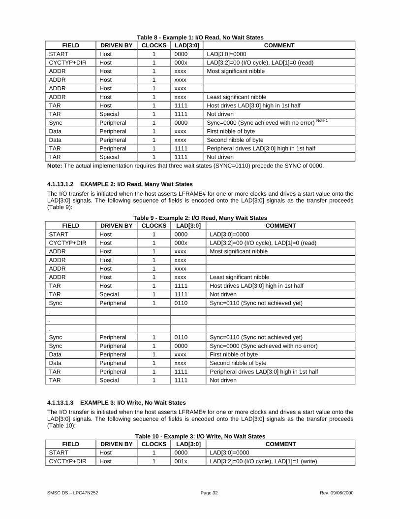
SMSC DS – LPC47N252 Page 32 Rev. 09/06/2000
Table 8 - Example 1: I/O Read, No Wait StatesFIELD DRIVEN BY CLOCKS LAD[3:0] COMMENT
START Host 1 0000 LAD[3:0]=0000
CYCTYP+DIR Host 1 000x LAD[3:2]=00 (I/O cycle), LAD[1]=0 (read)
ADDR Host 1 xxxx Most significant nibble
ADDR Host 1 xxxx
ADDR Host 1 xxxx
ADDR Host 1 xxxx Least significant nibble
TAR Host 1 1111 Host drives LAD[3:0] high in 1st half
TAR Special 1 1111 Not driven
Sync Peripheral 1 0000 Sync=0000 (Sync achieved with no error) Note 1
Data Peripheral 1 xxxx First nibble of byte
Data Peripheral 1 xxxx Second nibble of byte
TAR Peripheral 1 1111 Peripheral drives LAD[3:0] high in 1st half
TAR Special 1 1111 Not driven
Note: The actual implementation requires that three wait states (SYNC=0110) precede the SYNC of 0000.
4.1.13.1.2 EXAMPLE 2: I/O Read, Many Wait States
The I/O transfer is initiated when the host asserts LFRAME# for one or more clocks and drives a start value onto theLAD[3:0] signals. The following sequence of fields is encoded onto the LAD[3:0] signals as the transfer proceeds(Table 9):
Table 9 - Example 2: I/O Read, Many Wait StatesFIELD DRIVEN BY CLOCKS LAD[3:0] COMMENT
START Host 1 0000 LAD[3:0]=0000
CYCTYP+DIR Host 1 000x LAD[3:2]=00 (I/O cycle), LAD[1]=0 (read)
ADDR Host 1 xxxx Most significant nibble
ADDR Host 1 xxxx
ADDR Host 1 xxxx
ADDR Host 1 xxxx Least significant nibble
TAR Host 1 1111 Host drives LAD[3:0] high in 1st half
TAR Special 1 1111 Not driven
Sync Peripheral 1 0110 Sync=0110 (Sync not achieved yet)
.
.
.
Sync Peripheral 1 0110 Sync=0110 (Sync not achieved yet)
Sync Peripheral 1 0000 Sync=0000 (Sync achieved with no error)
Data Peripheral 1 xxxx First nibble of byte
Data Peripheral 1 xxxx Second nibble of byte
TAR Peripheral 1 1111 Peripheral drives LAD[3:0] high in 1st half
TAR Special 1 1111 Not driven
4.1.13.1.3 EXAMPLE 3: I/O Write, No Wait States
The I/O transfer is initiated when the host asserts LFRAME# for one or more clocks and drives a start value onto theLAD[3:0] signals. The following sequence of fields is encoded onto the LAD[3:0] signals as the transfer proceeds(Table 10):
Table 10 - Example 3: I/O Write, No Wait StatesFIELD DRIVEN BY CLOCKS LAD[3:0] COMMENT
START Host 1 0000 LAD[3:0]=0000
CYCTYP+DIR Host 1 001x LAD[3:2]=00 (I/O cycle), LAD[1]=1 (write)

SMSC DS – LPC47N252 Page 33 Rev. 09/06/2000
FIELD DRIVEN BY CLOCKS LAD[3:0] COMMENT
ADDR Host 1 xxxx Most significant nibble
ADDR Host 1 xxxx
ADDR Host 1 xxxx
ADDR Host 1 xxxx Least significant nibble
Data Host 1 xxxx First nibble of byte
Data Host 1 xxxx Second nibble of byte
TAR Host 1 1111 Host drives LAD[3:0] high in 1st half
TAR Special 1 1111 Not driven
Sync Peripheral 1 0000 Sync=0000 (Sync achieved with no error) Note 2
TAR Peripheral 1 1111 Peripheral drives LAD[3:0] high in 1st half
TAR Special 1 1111 Not driven
Note: The actual implementation requires that two wait states (SYNC=0110) precede the SYNC of 0000.
4.1.13.2 DMA Cycles
4.1.13.2.1 EXAMPLE 4: 3-Byte DMA Write, 8-bit transfers (Data from peripheral to main memory - I/O read,memory write)
The DMA transfer begins when the peripheral encodes the following bit sequence onto the LDRQ# signal (Table 11):
Table 11 - Example 4: 3-Byte DMA Write LDRQ# EncodingBIT DRIVEN BY CLOCKS COMMENT
Start Peripheral 1 Start bit = 0
DMA Ch# (MSB) Peripheral 1 Channel 0-3 for 8-bit transfers
DMA Ch# Peripheral 1
DMA Ch# (LSB) Peripheral 1
ACT Peripheral 1 ACT = 1 (DMA Channel Active)
1 (deassert) Peripheral 1 Following this clock, the peripheral can encode an LDRQ#sequence for another channel# (note)
Note: Peripheral deasserts LDRQ# for this channel for 8 clocks after it issues a SYNC of 0000.
The transfer continues when the host asserts LFRAME# for one or more clocks and drives a start value onto theLAD[3:0] signals. The following sequence of fields is encoded onto the LAD[3:0] signals as the transfer proceeds(Table 12):
Table 12 - Example 4 (Continued): LAD[3:0] EncodingFIELD DRIVEN BY CLOCKS LAD[3:0] COMMENT
START Host 1 0000 LAD[3:0]=0000 - First Byte -
CYCTYP+DIR Host 1 101x LAD[3:2]=10 (DMA), LAD[1]=1 (write)
CHANNEL Host 1 0xxx LAD[3]=0, LAD[2:0] = Ch # (acts as DMA Ack)
SIZE Host 1 xx00 LAD[1:0]=00 (8-bit)
TAR Host 1 1111 Host drives LAD[3:0] high in 1st half
TAR Special 1 1111 Not driven
Sync Peripheral 1 1001 Sync=1001 (more transfers req’d) Note 3
Data Peripheral 1 xxxx First nibble of first byte
Data Peripheral 1 xxxx Second nibble of first byte
TAR Peripheral 1 1111 Peripheral drives LAD[3:0] high in 1st half
TAR Special 1 1111 Not driven
The cycles below may not immediately follow. (Note 4)
START Host 1 0000 LAD[3:0]=0000 - Second Byte -
CYCTYP+DIR Host 1 101x LAD[3:2]=10 (DMA), LAD[1]=1 (write)
CHANNEL Host 1 0xxx LAD[3]=0, LAD[2:0] = Ch # (acts as DMA Ack)
SIZE Host 1 xx00 LAD[1:0]=00 (8-bit)

SMSC DS – LPC47N252 Page 34 Rev. 09/06/2000
FIELD DRIVEN BY CLOCKS LAD[3:0] COMMENT
TAR Host 1 1111 Host drives LAD[3:0] high in 1st half
TAR Special 1 1111 Not driven
Sync Peripheral 1 1001 Sync=1001 (more transfers req’d) Note 3
Data Peripheral 1 xxxx First nibble of second byte
Data Peripheral 1 xxxx Second nibble of second byte
TAR Peripheral 1 1111 Peripheral drives LAD[3:0] high in 1st half
TAR Special 1 1111 Not driven
The cycles below may not immediately follow. (Note 4)
START Host 1 0000 LAD[3:0]=0000 - Third Byte -
CYCTYP+DIR Host 1 101x LAD[3:2]=10 (DMA), LAD[1]=1 (write)
CHANNEL Host 1 1xxx LAD[3]=1 = TC (last byte of transfer), LAD[2:0] = Ch #
SIZE Host 1 xx00 LAD[1:0]=00 (8-bit)
TAR Host 1 1111 Host drives LAD[3:0] high in 1st half
TAR Special 1 1111 Not driven
Sync Peripheral 1 0000 Sync=0000 (no more transfers req’d) Note 3
Data Peripheral 1 xxxx First nibble of third byte
Data Peripheral 1 xxxx Second nibble of third byte
TAR Peripheral 1 1111 Peripheral drives LAD[3:0] high in 1st half
TAR Special 1 1111 Not driven
Note 3: The actual implementation requires that four wait states (SYNC=0101) precede this SYNC.
Note 4: These DMA cycles can be interspersed with I/O cycles, memory cycles or other DMA cycles.
4.1.13.2.2 EXAMPLE 5: 3 Byte DMA Read, 8-bit transfers (Data from main memory to peripheral - memoryread, I/O write)
The DMA transfer begins when the peripheral encodes the following bit sequence onto the LDRQ# signal (Table 13):
Table 13 -Example 5: 3-Byte DMA Read LDRQ# EncodingBIT DRIVEN BY CLOCKS COMMENT
Start Peripheral 1 Start bit = 0
DMA Ch# (MSB) Peripheral 1 Channel 0-3 for 8-bit transfers
DMA Ch# (MB) Peripheral 1
DMA Ch# (LSB) Peripheral 1
ACT Peripheral 1 ACT = 1 (DMA Channel Active)
1 (deassert) Peripheral 1 Following this clock, the peripheral can encode an LDRQ#sequence for another channel#
The transfer continues when the host asserts LFRAME# for one or more clocks and drives a start value onto theLAD[3:0] signals. The following sequence of fields is encoded onto the LAD[3:0] signals as the transfer proceeds(Table 14):
Table 14 - Example 5 (Continued) LAD[3:0] EncodingFIELD DRIVEN BY CLOCKS LAD[3:0] COMMENT
START Host 1 0000 LAD[3:0]=0000 - First Byte -
CYCTYP+DIR Host 1 100x LAD[3:2]=10 (DMA), LAD[1:0]=0 (read)
CHANNEL Host 1 0xxx LAD[3]=0, LAD[2:0] = Ch # (acts as DMA Ack)
SIZE Host 1 xx00 LAD[1:0]=00 (8-bit)
Data Host 1 xxxx First nibble of first byte
Data Host 1 xxxx Second nibble of first byte
TAR Host 1 1111 Host drives LAD[3:0] high in 1st half
TAR Special 1 1111 Not Driven
SYNC Peripheral 1 1001 Sync=1001 (more transfers req’d) Note 5
TAR Peripheral 1 1111 Peripheral drives LAD[3:0] high in 1st half
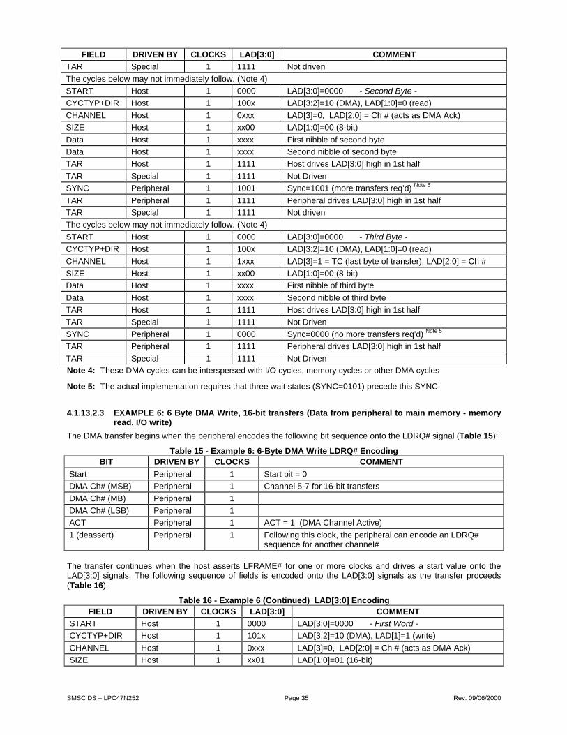
SMSC DS – LPC47N252 Page 35 Rev. 09/06/2000
FIELD DRIVEN BY CLOCKS LAD[3:0] COMMENT
TAR Special 1 1111 Not driven
The cycles below may not immediately follow. (Note 4)
START Host 1 0000 LAD[3:0]=0000 - Second Byte -
CYCTYP+DIR Host 1 100x LAD[3:2]=10 (DMA), LAD[1:0]=0 (read)
CHANNEL Host 1 0xxx LAD[3]=0, LAD[2:0] = Ch # (acts as DMA Ack)
SIZE Host 1 xx00 LAD[1:0]=00 (8-bit)
Data Host 1 xxxx First nibble of second byte
Data Host 1 xxxx Second nibble of second byte
TAR Host 1 1111 Host drives LAD[3:0] high in 1st half
TAR Special 1 1111 Not Driven
SYNC Peripheral 1 1001 Sync=1001 (more transfers req’d) Note 5
TAR Peripheral 1 1111 Peripheral drives LAD[3:0] high in 1st half
TAR Special 1 1111 Not driven
The cycles below may not immediately follow. (Note 4)
START Host 1 0000 LAD[3:0]=0000 - Third Byte -
CYCTYP+DIR Host 1 100x LAD[3:2]=10 (DMA), LAD[1:0]=0 (read)
CHANNEL Host 1 1xxx LAD[3]=1 = TC (last byte of transfer), LAD[2:0] = Ch #
SIZE Host 1 xx00 LAD[1:0]=00 (8-bit)
Data Host 1 xxxx First nibble of third byte
Data Host 1 xxxx Second nibble of third byte
TAR Host 1 1111 Host drives LAD[3:0] high in 1st half
TAR Special 1 1111 Not Driven
SYNC Peripheral 1 0000 Sync=0000 (no more transfers req’d) Note 5
TAR Peripheral 1 1111 Peripheral drives LAD[3:0] high in 1st half
TAR Special 1 1111 Not Driven
Note 4: These DMA cycles can be interspersed with I/O cycles, memory cycles or other DMA cycles
Note 5: The actual implementation requires that three wait states (SYNC=0101) precede this SYNC.
4.1.13.2.3 EXAMPLE 6: 6 Byte DMA Write, 16-bit transfers (Data from peripheral to main memory - memoryread, I/O write)
The DMA transfer begins when the peripheral encodes the following bit sequence onto the LDRQ# signal (Table 15):
Table 15 - Example 6: 6-Byte DMA Write LDRQ# EncodingBIT DRIVEN BY CLOCKS COMMENT
Start Peripheral 1 Start bit = 0
DMA Ch# (MSB) Peripheral 1 Channel 5-7 for 16-bit transfers
DMA Ch# (MB) Peripheral 1
DMA Ch# (LSB) Peripheral 1
ACT Peripheral 1 ACT = 1 (DMA Channel Active)
1 (deassert) Peripheral 1 Following this clock, the peripheral can encode an LDRQ#sequence for another channel#
The transfer continues when the host asserts LFRAME# for one or more clocks and drives a start value onto theLAD[3:0] signals. The following sequence of fields is encoded onto the LAD[3:0] signals as the transfer proceeds(Table 16):
Table 16 - Example 6 (Continued) LAD[3:0] EncodingFIELD DRIVEN BY CLOCKS LAD[3:0] COMMENT
START Host 1 0000 LAD[3:0]=0000 - First Word -
CYCTYP+DIR Host 1 101x LAD[3:2]=10 (DMA), LAD[1]=1 (write)
CHANNEL Host 1 0xxx LAD[3]=0, LAD[2:0] = Ch # (acts as DMA Ack)
SIZE Host 1 xx01 LAD[1:0]=01 (16-bit)
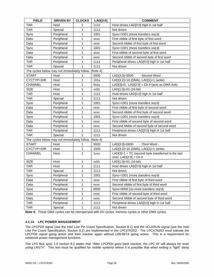
SMSC DS – LPC47N252 Page 36 Rev. 09/06/2000
FIELD DRIVEN BY CLOCKS LAD[3:0] COMMENT
TAR Host 1 1111 Host drives LAD[3:0] high in 1st half
TAR Special 1 1111 Not driven
Sync Peripheral 1 1001 Sync=1001 (more transfers req’d)
Data Peripheral 1 xxxx First nibble of first byte of first word
Data Peripheral 1 xxxx Second nibble of first byte of first word
Sync Peripheral 1 1001 Sync=1001 (more transfers req’d)
Data Peripheral 1 xxxx First nibble of second byte of first word
Data Peripheral 1 xxxx Second nibble of second byte of first word
TAR Peripheral 1 1111 Peripheral drives LAD[3:0] high in 1st half
TAR Special 1 1111 Not driven
The cycles below may not immediately follow. (Note 4)
START Host 1 0000 LAD[3:0]=0000 - Second Word -
CYCTYP+DIR Host 1 101x LAD[3:2]=10 (DMA), LAD[1]=1 (write)
CHANNEL Host 1 0xxx LAD[3]=0, LAD[2:0] = Ch # (acts as DMA Ack)
SIZE Host 1 xx01 LAD[1:0]=01 (16-bit)
TAR Host 1 1111 Host drives LAD[3:0] high in 1st half
TAR Special 1 1111 Not driven
Sync Peripheral 1 1001 Sync=1001 (more transfers req’d)
Data Peripheral 1 xxxx First nibble of first byte of second word
Data Peripheral 1 xxxx Second nibble of first byte of second word
Sync Peripheral 1 1001 Sync=1001 (more transfers req’d)
Data Peripheral 1 xxxx First nibble of second byte of second word
Data Peripheral 1 xxxx Second nibble of second byte of second word
TAR Peripheral 1 1111 Peripheral drives LAD[3:0] high in 1st half
TAR Special 1 1111 Not driven
The cycles below may not immediately follow. (Note 4)
START Host 1 0000 LAD[3:0]=0000 - Third Word -
CYCTYP+DIR Host 1 1000 LAD[3:2]=10 (DMA), LAD[1]=1 (write)
CHANNEL Host 1 1xxx LAD[3]=1 = TC (second byte transferred is the lastone) LAD[2:0] = Ch #
SIZE Host 1 xx01 LAD[1:0]=01 (16-bit)
TAR Host 1 1111 Host drives LAD[3:0] high in 1st half
TAR Special 1 1111 Not driven
Sync Peripheral 1 1001 Sync=1001 (more transfers req’d)
Data Peripheral 1 xxxx First nibble of first byte of third word
Data Peripheral 1 xxxx Second nibble of first byte of third word
Sync Peripheral 1 0000 Sync=0000 (no more transfers req’d)
Data Peripheral 1 xxxx First nibble of second byte of third word
Data Peripheral 1 xxxx Second nibble of second byte of third word
TAR Peripheral 1 1111 Peripheral drives LAD[3:0] high in 1st half
TAR Special 1 1111 Not driven
Note 4: These DMA cycles can be interspersed with I/O cycles, memory cycles or other DMA cycles.
4.1.14 LPC POWER MANAGEMENT
The LPCPD# signal (see the Intel Low Pin Count Specification, Section 8.1) and the nCLKRUN signal (see the IntelLow Pin Count Specification, Section 8.2) are implemented in the LPC47N252. The LPC47N252 must tolerate theLPCPD# signal going active and then inactive again without LRESET# going active. This is a requirement fornotebook power management functions.
The LPC Bus spec 1.0 section 8.2 states that "After LPCPD# goes back inactive, the LPC I/F will always be resetusing LRST#”. This text must be qualified for mobile systems where it is possible that when exiting a "light" sleep

SMSC DS – LPC47N252 Page 37 Rev. 09/06/2000
state (ACPI S1, APM POS), LPCPD# may be asserted but the LPC Bus power may not be removed, in which caseLRESET# will not occur. When exiting a "deeper" sleep state (ACPI S3-S5, APM STR, STD, soft-off), LRESET# willoccur.
The LPCPD# pin is implemented as a “local” powergood for the LPC bus in the LPC47N252. It is not to be used as aglobal powergood for the chip. It is used to minimize the LPC power dissipation. It should be used to reset the LPCblock and hold it in reset.
Prior to going to a low-power state, the system asserts the LPCPD# signal. LPCPD# goes active at least 30microseconds prior to the LCLK signal stopping low and power being shut to the other LPC interface signals. Uponrecognizing LPCPD# active, there are no further transactions on the LPC interface. The LPC47N252 drives theLDRQ# signal low or tri-state, and does so until LPCPD# goes active. This prevents The LPC47N252 from driving thesignals high into a potentially powered-down host.
Upon recognizing LPCPD# inactive, The LPC47N252 drives LDRQ# high.

SMSC DS – LPC47N252 Page 38 Rev. 09/06/2000
5 FLOPPY DISK CONTROLLER
The Floppy Disk Controller (FDC) provides the interface between a host microprocessor and the Floppy Disk Drives(FDD). The FDC integrates the functions of the formatter/controller, Digital Data Separator, Write Precompensationand data rate Selection logic for an IBM XT/AT compatible FDC. The true CMOS 765B core guarantees 100% IBMPC XT/AT compatibility in addition to providing data overflow and underflow protection.
The FDC is compatible to the 82077AA using SMSC's proprietary FDC core.
FDC INTERNAL REGISTERS
The FDC contains eight internal registers, which facilitate the interfacing between the host microprocessor and thedisk drive Table 17 shows the addresses required to access these registers. Registers other than the ones shownare not supported.
Table 17 - Status, Data And Control RegistersFDC PRIMARY BASE I/O
ADDRESS OFFSETPRIMARY
ADDRESS R/W REGISTER
0 3F0 R Status Register A (SRA)
1 3F1 R Status Register B (SRB)
2 3F2 R/W Digital Output Register (DOR)
3 3F3 R/W Tape Drive Register (TDR)
4 3F4 R Main Status Register (MSR)
4 3F4 W Data Rate Select Register (DSR)
5 3F5 R/W Data (FIFO)
6 3F6 Reserved
7 3F7 R Digital Input Register (DIR)
7 3F7 W Configuration Control Register (CCR)
STATUS REGISTER A (SRA)
F DC I/O Base Ad d ress + 0x00 ( R EA D ONL Y) This register is read-only and monitors the state of the internal FDC interrupt signal and several disk interface pins inPS/2 and Model 30 modes. The SRA can be accessed at any time when in PS/2 mode. In the PC/AT mode the databus pins D0 - D7 are held in a high impedance state for a read of SRA.
Table 18 - SRA-PS/2 Mode7 6 5 4 3 2 1 0
INT PEN DIN G
nDR V2 STEP nTR K0 H DSEL nIN DX nWP D IR
R ESET
C ON D.
0 N /A 0 N /A 0 N /A N /A 0
BIT 0 DIRECTIONActive high status indicating the direction of head movement. A logic "1" indicates inward direction; a logic "0"indicates outward direction.
BIT 1 nWRITE PROTECTActive low status of the WRITE PROTECT disk interface input. A logic "0" indicates that the disk is write protected.
BIT 2 nINDEXActive low status of the INDEX disk interface input.
BIT 3 HEAD SELECTActive high status of the HDSEL disk interface input. A logic "1" selects side 1 and a logic "0" selects side 0.
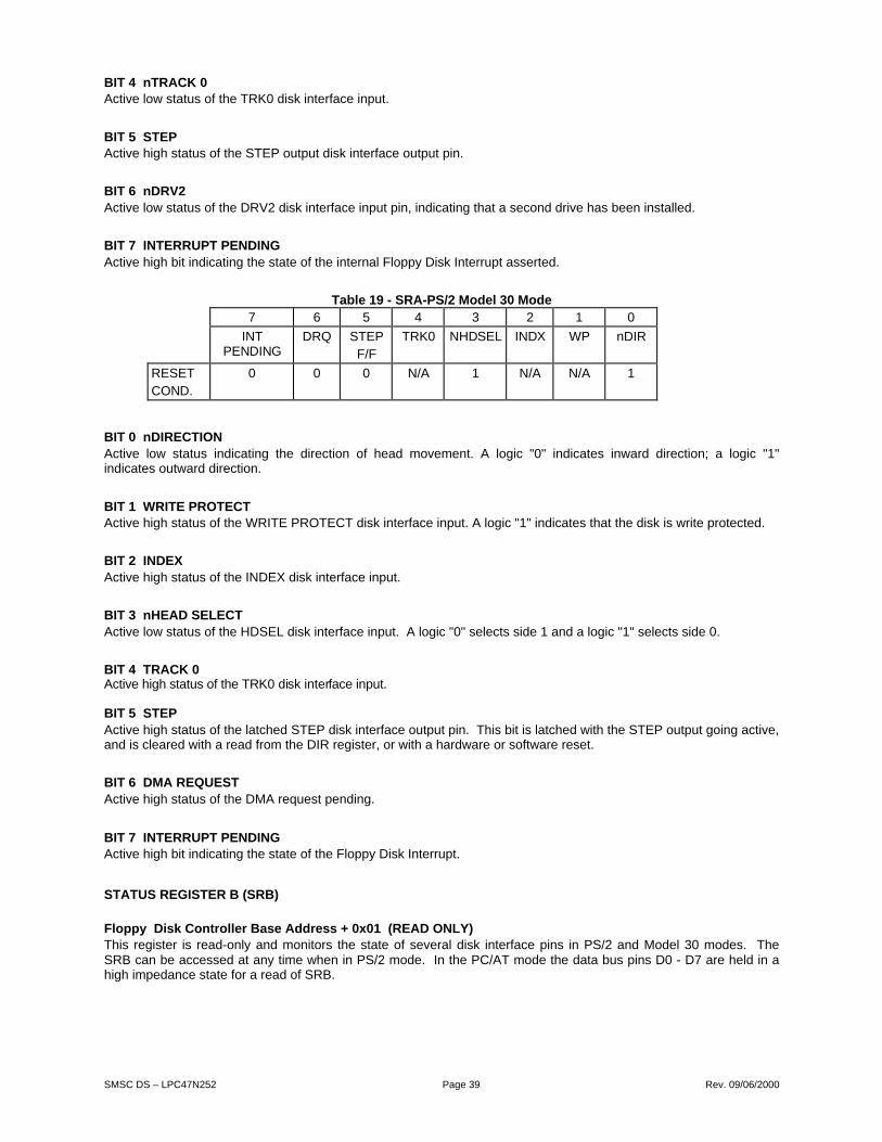
SMSC DS – LPC47N252 Page 39 Rev. 09/06/2000
BIT 4 nTRACK 0Active low status of the TRK0 disk interface input.
BIT 5 STEPActive high status of the STEP output disk interface output pin.
BIT 6 nDRV2Active low status of the DRV2 disk interface input pin, indicating that a second drive has been installed.
BIT 7 INTERRUPT PENDINGActive high bit indicating the state of the internal Floppy Disk Interrupt asserted.
Table 19 - SRA-PS/2 Model 30 Mode7 6 5 4 3 2 1 0
INT PEN DIN G
D RQ STEPF /F
T RK0 N HD SEL IND X W P nDIR
R ESET C ON D.
0 0 0 N /A 1 N /A N /A 1
BIT 0 nDIRECTIONActive low status indicating the direction of head movement. A logic "0" indicates inward direction; a logic "1"indicates outward direction.
BIT 1 WRITE PROTECTActive high status of the WRITE PROTECT disk interface input. A logic "1" indicates that the disk is write protected.
BIT 2 INDEXActive high status of the INDEX disk interface input.
BIT 3 nHEAD SELECTActive low status of the HDSEL disk interface input. A logic "0" selects side 1 and a logic "1" selects side 0.
BIT 4 TRACK 0Active high status of the TR K0 di sk inter face input.
BIT 5 STEPActive high status of the latched STEP disk interface output pin. This bit is latched with the STEP output going active,and is cleared with a read from the DIR register, or with a hardware or software reset.
BIT 6 DMA REQUESTActive high status of the DMA request pending.
BIT 7 INTERRUPT PENDINGActive high bit indicating the state of the Floppy Disk Interrupt.
STATUS REGISTER B (SRB)
Floppy Disk Controller Base Address + 0x01 (READ ONLY)This register is read-only and monitors the state of several disk interface pins in PS/2 and Model 30 modes. TheSRB can be accessed at any time when in PS/2 mode. In the PC/AT mode the data bus pins D0 - D7 are held in ahigh impedance state for a read of SRB.

SMSC DS – LPC47N252 Page 40 Rev. 09/06/2000
Table 20 - FDC SRB -PS/2 M o de
7 6 5 4 3 2 1 0
1 1 D RIVESEL0
W DATAT OGGLE
R DATAT OGGLE
W GATE M OT EN1
M OT EN0
R ESET C ON D.
1 1 0 0 0 0 0 0
BIT 0 MOTOR ENABLE 0Active high status of the MTR0 disk interface output pin. This bit is low after a hardware reset and unaffected by asoftware reset.
BIT 1 MOTOR ENABLE 1Active high status of the MTR1 disk interface output pin. This bit is low after a hardware reset and unaffected by asoftware reset.
BIT 2 WRITE GATEActive high status of the WGATE disk interface output.
BIT 3 READ DATA TOGGLEEvery inactive edge of the RDATA input causes this bit to change state.
BIT 4 WRITE DATA TOGGLEEvery inactive edge of the WDATA output causes this bit to change state.
BIT 5 DRIVE SELECT 0Reflects the status of the Drive Select 0 bit of the DOR (address 3F2 bit 0). This bit is cleared after a hardware resetand it is unaffected by a software reset.
BIT 6 RESERVEDAlways read as a logic “1”.
BIT 7 RESERVEDAlways read as a logic “1”.
Table 21 - FDC SRB-PS/2 Model 30 Mode7 6 5 4 3 2 1 0
nDR V2 nDS1 nDS0 W DATAF /F
R DATAF /F
W GATEF /F
nDS3 nDS2
R ESET C ON D.
N /A 1 1 0 0 0 1 1
BIT 0 nDRIVE SELECT 2Active low status of the DS2 disk interface output.
BIT 1 nDRIVE SELECT 3Active low status of the DS3 disk interface output.
BIT 2 WRITE GATEActive high status of the latched WGATE output signal. This bit is latched by the active going edge of WGATE and iscleared by the read of the DIR register.

SMSC DS – LPC47N252 Page 41 Rev. 09/06/2000
BIT 3 READ DATAActive high status of the latched RDATA input signal. This bit is latched by the inactive going edge of RDATA and iscleared by the read of the DIR register.
BIT 4 WRITE DATAActive high status of the latched WDATA output signal. This bit is latched by the inactive going edge of WDATA andis cleared by the read of the DIR register. This bit is not gated with WGATE.
BIT 5 nDRIVE SELECT 0Active low status of the DS0 disk interface output.
BIT 6 nDRIVE SELECT 1Active low status of the DS1 disk interface output.
BIT 7 nDRV2Active low status of the DRV2 disk interface input.
DIGITAL OUTPUT REGISTER (DOR)
FDC I/O Base Address + 0x02 (READ/WRITE)The DOR controls the drive select and motor enables of the disk interface outputs. It also contains the enable for theDMA logic and a software reset bit. The contents of the DOR are unaffected by a software reset. The DOR can bewritten to at any time.
Table 22 - FDC DOR7 6 5 4 3 2 1 0
MOTEN3
MOTEN2
MOTEN1
MOTEN0
DMAEN nRESET DRIVESEL1
DRIVESEL0
RESETCOND.
0 0 0 0 0 0 0 0
BIT 0 and 1 DRIVE SELECTThese two bits are binary encoded for the two drive selects output pins nds0 and nds1, thereby allowing only onedrive to be selected at one time.
BIT 2 nRESETA logic “0” written to this bit resets the FDC. This reset will remain active until a logic “1” is written to this bit. Thissoftware reset does not affect the DSR and CCR registers, nor does it affect the other bits of the DOR register. Theminimum reset duration required is 100ns, therefore toggling this bit by consecutive writes to this register is a validmethod of issuing a software reset.
BIT 3 DMAENPC/AT and Model 30 Mode: Writing this bit to logic “1” will enable the FDC’s DMA and interrupt functions This bitbeing a logic “0” will disable the FDC’s DMA and interrupt functions. This bit is a logic “0” after a reset.
PS/2 Mode: In this mode the FDC’s DMA and interrupt functions are always enabled. During a reset this bit will becleared to a logic “0”.
BIT 4 MOTOR ENABLE 0This bit controls the disk interface output. A logic “1” in this bit will cause the output pin to assert.
BIT 5 MOTOR ENABLE 1This bit controls the nMTR1 disk interface output. A logic “1” in this bit will cause the output pin to assert.
BIT 6 MOTOR ENABLE 2This bit controls the nMTR2 disk interface output. A logic “1” in this bit will cause the output pin to assert.

SMSC DS – LPC47N252 Page 42 Rev. 09/06/2000
BIT 7 MOTOR ENABLE 3This bit controls the nMTR3 disk interface output. A logic “1” in this bit will cause the output pin to assert.
Table 23 – FDC Drive Activation ValuesD RIVE D OR VA LU E
0
1
1CH
2DH
Table 24 - FDC Internal 2 Drive Decode-Normal
D IGIT A L OU T PUT R EGIST ERD R IVE SEL EC T OU T PUT S
( A CT IVE L OW ) M OTOR ON OU T PU T S
( A CT IVE L OW )
Bi t 7 Bi t 6 Bi t 5 Bi t 4 Bi t1 Bi t 0 nD S1 nD S0 nM TR 1 nM TR 0
X X X 1 0 0 1 0 nBIT 5 nBIT 4
X X 1 X 0 1 0 1 nBIT 5 nBIT 4
X 1 X X 1 0 1 1 nBIT 5 nBIT 4
1 X X X 1 1 1 1 nBIT 5 nBIT 4
0 0 0 0 X X 1 1 nBIT 5 nBIT 4
Table 25 - FDC Internal 2 Drive Decode-Drives 0 And 1 Swapped
D IGIT A L OU T PUT R EGIST ERD R IVE SEL EC T
OU TPU T S ( A C T IVE L OW ) M OTOR ON OU T PU T S
( A CT IVE L OW )
X X X 1 0 0 0 1 nBIT 4 nBIT 5
X X 1 X 0 1 1 0 nBIT 4 nBIT 5
X 1 X X 1 0 1 1 nBIT 4 nBIT 5
1 X X X 1 1 1 1 nBIT 4 nBIT 5
0 0 0 0 X X 1 1 nBIT 4 nBIT 5
TAPE DRIVE REGISTER (TDR)
FDC I/O Base Address + 0x03 (READ/WRITE)This register is included for 82077 software compatability. The TDR is unaffected by a software reset. The improveddata separator incorporates tape drive support and requires the Tape Select bits in the FDC Tape Drive register toidentify which drive has been assigned to receive this support (see the following section).
Normal Floppy ModeNormal mode. The TDR allows the user to assign tape support to a particular drive during initialization. Any futurereferences to that drive number automatically invokes tape support. The Tape Select bits are TDR[1:0]. The TDRRegister contains only bits 0 and 1. When this register is read, bits 2 – 7 are ‘0’.
Table 26 - FDC TDR Normal Floppy ModeD B7 D B6 D B5 D B4 D B3 D B2 D B1 D B0
R EG 3F 3 0 0 0 0 0 0 tape sel 1 tape sel 0

SMSC DS – LPC47N252 Page 43 Rev. 09/06/2000
TAPE SEL1(TDR.1)
TAPE SEL2(TDR.0)
DRIVESELECTED
0 0 None
0 1 1
1 0 2
1 1 3
Enhanced Floppy Mode 2 (OS2)
The TDR Register for Enhanced Floppy Mode 2 operation.
Table 27 - FDC TDR Enh an ced F lop py Mo de 2 (OS2) D B7 D B6 D B5 D B4 D B3 D B2 D B1 D B0
R EG 3F 3 1 1 D ri ve Type ID F loppy Boot D ri ve tape sel 1 tape sel 0
BIT 7 This bit is always set active high
BIT 6 This bit is always set active high
BITS 5 and 4 Drive Type IDThese bits reflect two of the bits of L0-CRF1 (Logical Device 0 – Configuration Register 0xF1). Which two bitsthese are depends on the last drive selected in the Digital Output Register. (See Table 32)
BITS 3 and 2 Floppy Boot DriveThese bits reflect two of the bits of L0-CRF1. Bit 3 = L0-CRF1-B7. Bit 2 = L0-CRF1-B6.
BIT 1 and 0 – Tape Drive Select (R EAD /W RIT E) Same as in Normal and Enhanced Floppy Mode 2.
Table 28 – Drive Type IDD IGIT A L OU T PU T R EGIST ER T DR R EGIST ER – D RIVE TYPE ID
Bit 1 Bit 0 Bit 5 Bit 4
0 0 L0- CR F 2 – B1 L0- CR F 2 – B0
0 1 L0- CR F 2 – B3 L0- CR F 2 – B2
1 0 L0- CR F 2 – B5 L0- CR F 2 – B4
1 1 L0- CR F 2 – B7 L0- CR F 2 – B6Note: L0-CRF2-Bx = Logical Device 0, Configuration Register F2, Bit x.
MID[1:0] FDD Interface PinsThe FDC Media ID pins are not supported in the LPC47N252. The MID[1:0] inputs to the FDC core are strapped sothat the Media ID bits the TDR are always “high”.
DATA RATE SELECT REGISTER (DSR)
F DC I/O Base Ad d ress + 0x04 ( W RITE ON LY) This register is write only. It is used to program the data rate, amount of write precompensation, power down status,and software reset. The data rate is programmed using the Configuration Control Register (CCR) not the DSR, forPC/AT and PS/2 Model 30. Other applications can set the data rate in the DSR. The data rate of the floppy controlleris the most recent write of either the DSR or CCR. The DSR is unaffected by a software reset. A hardware reset willset the DSR to 02H, which corresponds to the default precompensation setting and 250 Kbps.
Table 29 - FDC DSR7 6 5 4 3 2 1 0
S/W R ESET
POW ER D OW N
0 PRE-C OM P2
PRE-C OM P1
PRE-C OM P0
D RATESEL1
D RATESEL0
R ESET
C ON D.
0 0 0 0 0 0 1 0

SMSC DS – LPC47N252 Page 44 Rev. 09/06/2000
BITS 0 - 1 DATA RATE SELECTThese bits control the data rate of the floppy controller. See Table 31 for the settings corresponding to the individualdata rates. The data rate select bits are unaffected by a software reset and are set to 250 Kbps after a hardwarereset.
B IT S 2 - 4 PREC OM PEN SA TION SEL EC TThese three bits select the value of write precompensation that will be applied to the WDATA output signal. Table 30shows the precompensation values for the combination of these bits settings. Track 0 is the default starting tracknumber to start precompensation. This starting track number can be changed by the configure command.
BIT 5 UNDEFINEDShould be written as a logic "0".
BIT 6 LOW POWERA logic "1" written to this bit will put the floppy controller into manual low power mode. The floppy controller clock anddata separator circuits will be turned off. The controller will come out of manual low power mode after a softwarereset or access to the Data Register or Main Status Register.
BIT 7 SOFTWARE RESETThis active high bit has the same function as the DOR RESET (DOR bit 2) except that this bit is self clearing.
Table 30 - FDC Precompensation Delays
PRECOM P 432
PRECOM PENSA TION DELA Y( nsec)
<2M bps 2Mbps
111
001010
011100101
110000
0.00
41.6783.34
125.00166.67208.33
250.00D efaul t
0
20.841.7
62.583.3104.2
125D efaul t
Default: See Table 28
Table 31 - FDC Data RatesD RIVE RA TE D AT A R AT E D AT A R AT E D EN SEL D RA TE( 1)
D RT 1 D RT 0 SEL 1 SEL 0 M FM F M 1 0
0 0 1 1 1Meg - -- 1 1 1
0 0 0 0 500 250 1 0 0
0 0 0 1 300 150 0 0 1
0 0 1 0 250 125 0 1 0
0 1 1 1 1Meg - -- 1 1 1
0 1 0 0 500 250 1 0 0
0 1 0 1 500 250 0 0 1
0 1 1 0 250 125 0 1 0
1 0 1 1 1Meg - -- 1 1 1
1 0 0 0 500 250 1 0 0
1 0 0 1 2Meg - -- 0 0 1
1 0 1 0 250 125 0 1 0
Drive Rate Table (Recommended) 00 = 360K, 1.2M, 720K, 1.44M and 2.88M Vertical Format
01 = 3-Mode Drive
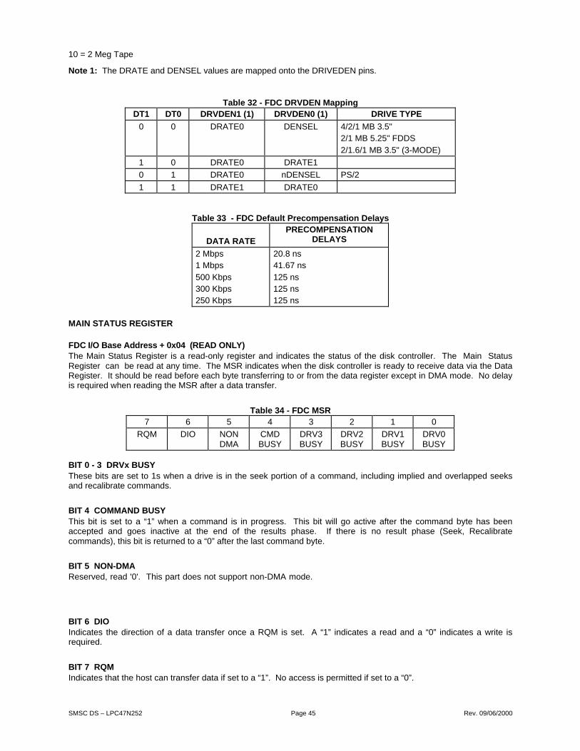
SMSC DS – LPC47N252 Page 45 Rev. 09/06/2000
10 = 2 Meg Tape
Note 1: The DRATE and DENSEL values are mapped onto the DRIVEDEN pins.
Table 32 - FDC DRVDEN MappingDT1 DT0 DRVDEN1 (1) DRVDEN0 (1) DRIVE TYPE
0 0 DRATE0 DENSEL 4/2/1 MB 3.5"2/1 MB 5.25" FDDS
2/1.6/1 MB 3.5" (3-MODE)
1 0 DRATE0 DRATE1
0 1 DRATE0 nDENSEL PS/2
1 1 DRATE1 DRATE0
Table 33 - FDC Default Precompensation Delays
DATA RATEPRECOMPENSATION
DELAYS
2 Mbps1 Mbps
500 Kbps300 Kbps250 Kbps
20.8 ns41.67 ns
125 ns125 ns125 ns
MAIN STATUS REGISTER
F DC I/O Base Ad d ress + 0x04 ( R EA D ONL Y) The Main Status Register is a read-only register and indicates the status of the disk controller. The Main StatusRegister can be read at any time. The MSR indicates when the disk controller is ready to receive data via the DataRegister. It should be read before each byte transferring to or from the data register except in DMA mode. No delayis required when reading the MSR after a data transfer.
Table 34 - FDC MSR7 6 5 4 3 2 1 0
RQM DIO NONDMA
CMDBUSY
DRV3BUSY
DRV2BUSY
DRV1BUSY
DRV0BUSY
BIT 0 - 3 DRVx BUSYThese bits are set to 1s when a drive is in the seek portion of a command, including implied and overlapped seeksand recalibrate commands.
BIT 4 COMMAND BUSYThis bit is set to a “1” when a command is in progress. This bit will go active after the command byte has beenaccepted and goes inactive at the end of the results phase. If there is no result phase (Seek, Recalibratecommands), this bit is returned to a “0” after the last command byte.
BIT 5 NON-DMAReserved, read '0'. This part does not support non-DMA mode.
BIT 6 DIOIndicates the direction of a data transfer once a RQM is set. A “1” indicates a read and a “0” indicates a write isrequired.
BIT 7 RQMIndicates that the host can transfer data if set to a “1”. No access is permitted if set to a “0”.

SMSC DS – LPC47N252 Page 46 Rev. 09/06/2000
DATA REGISTER (FIFO)
FDC I/O Base Address + 0x05 (READ/WRITE)All command parameter information, disk data and result status are transferred between the host processor and theFDC through the Data Register. Data transfers are governed by the RQM and DIO bits in the Main Status Register.
The Data Register defaults to FIFO disabled mode after any form of reset. This maintains PC/AT hardwarecompatibility. The default values can be changed through the Configure command (enable full FIFO operation withthreshold control). The advantage of the FIFO is that it allows the system a larger DMA latency without causing adisk error.
Table 43 gives several examples of the delays with a FIFO. The data is based upon the following formula:
Threshold # x [8/DATA RATE] - 1.5ms = Delay
At the start of a command, the FIFO action is always disabled and command parameters must be sent based uponthe RQM and DIO bit settings. As the command execution phase is entered, the FIFO is cleared of any data toensure that invalid data is not transferred.
An overrun or underrun will terminate the current command and the transfer of data. Disk writes will complete thecurrent sector by generating a 00 pattern and valid CRC. Reads require the host to remove the remaining data sothat the result phase may be entered.
Table 35 - FIFO Service DelayF IF O T HR ESH OL DEXA MPL ES
M AXIM U M DEL AY T O SER VIC IN G A T2 M bp s* DA T A RA T E
1 byte
2 bytes8 bytes
15 bytes
1 x 4 ms - 1.5 m s = 2.5 m s
2 x 4 ms - 1.5 m s = 6.5 m s8 x 4 ms - 1.5 m s = 30.5 m s
15 x 4 m s - 1.5 ms = 58.5 ms
F IF O T HR ESH OL DEXA MPL ES
M AXIM U M DEL AY T O SER VIC IN G A T1 M bp s D AT A R AT E
1 byte2 bytes
8 bytes15 bytes
1 x 8 ms - 1.5 m s = 6.5 m s2 x 8 ms - 1.5 m s = 14.5 m s
8 x 8 ms - 1.5 m s = 62.5 m s15 x 8 m s - 1.5 ms = 118.5 m s
F IF O T HR ESH OL DEXA MPL ES
M AXIM U M DEL AY T O SER VIC IN G A T500 K b ps D A TA R A TE
1 byte2 bytes
8 bytes15 bytes
1 x 16 m s - 1.5 ms = 14.5 ms2 x 16 m s - 1.5 ms = 30.5 ms
8 x 16 m s - 1.5 ms = 126.5 m s15 x 16 ms - 1.5 m s = 238.5 ms
DIGITAL INPUT REGISTER (DIR)
FDC I/O Base Address + 0x07 (READ ONLY)This register is read-only in all modes.
DIR - PC-AT Mode
Table 36 - FDC DIR all modes7 6 5 4 3 2 1 0
DSKCHG
RESETCOND.
N/A N/A N/A N/A N/A N/A N/A N/A

SMSC DS – LPC47N252 Page 47 Rev. 09/06/2000
BIT 0 – 6 UNDEFINEDThe data bus outputs D0 – 6 are read as ‘0’.
BIT 7 DSKCHGThis bit monitors the pin of the same name and reflects the opposite value seen on the disk cable or the valueprogrammed in the Disk Change Register (see section 19.8, FDC Shadow Registers System on page 229.)
DIR – PS/2 Mode
Table 37 - FDC DIR PS/2 Mode7 6 5 4 3 2 1 0
DSKCHG
1 1 1 1 DRATESEL1
DRATESEL0
nhighDENS
RESETCOND.
N/A N/A N/A N/A N/A N/A N/A 1
BIT 0 nHIGHNhigh DENSThis bit is low whenever the 500 Kbps or 1 Mbps data rates are selected, and high when 250 Kbps and 300 Kbps areselected.
BITS 1 – 2 DATA RATE SELECTThese bits control the data rate of the floppy controller. See Table 31 for the settings corresponding to the individualdata rates. The data rate select bits are unaffected by a software reset, and are set to 250 Kbps after a hardwarereset.
BITS 3 – 6 UNDEFINEDAlways read as a logic “1”
BIT 7 DSKCHGThis bit monitors the pin of the same name and reflects the opposite value seen on the disk cable or the valueprogrammed in the Disk Change Register (see section 19.8, FDC Shadow Registers System on page 229).
D IR – Mo del 30 M od e
Table 38 - FDC DIR Model 30 Mode7 6 5 4 3 2 1 0
DSKCHG
0 0 0 DMAEN NOPREC DRATESEL1
DRATESEL0
RESETCOND.
N/A 0 0 0 0 0 1 0
BITS 0 and 1 DATA RATE SELECTThese bits control the data rate of the floppy controller. See Table 31 for the settings corresponding to the individualdata rates. The data rate select bits are unaffected by a software reset and are set to 250 Kbps after a hardwarereset.
BIT 2 NOPRECThis bit reflects the value of NOPREC bit set in the CCR register.
BIT 3 DMAENThis bit reflects the value of DMAEN bit set in the DOR register bit 3.
B IT S 4 - 6 UN D EF IN EDAlways read as a logic "0"

SMSC DS – LPC47N252 Page 48 Rev. 09/06/2000
BIT 7 DSKCHGThis bit monitors the pin of the same name and reflects the opposite value seen on the disk cable or the valueprogrammed in the Disk Change Register (see section 19.8, FDC Shadow Registers System on page 229.)
CONFIGURATION CONTROL REGISTER (CCR)
FDC I/O Base Address + 0x07 (WRITE ONLY)
Table 39 - FDC CCR PC/AT an d PS/2 M od e
7 6 5 4 3 2 1 0
D RATESEL1
D RATESEL0
R ESET C ON D.
N /A N /A N /A N /A N /A N /A 1 0
BIT 0 and 1 DATA RATE SELECT 0 and 1These bits determine the data rate of the floppy controller. See Table 31 for the appropriate values.
BIT 2 - 7 RESERVEDShould be set to a logical "0"
Table 40 - FDC CCR - PS/2 M od el 30 M o de
7 6 5 4 3 2 1 0
N OPREC D RATESEL1
D RATESEL0
R ESET C ON D.
N /A N /A N /A N /A N /A N /A 1 0
BIT 0 and 1 DATA RATE SELECT 0 and 1These bits determine the data rate of the floppy controller. See Table 31 for the appropriate values.
BIT 2 NO PRECOMPENSATIONThis bit can be set by software, but it has no functionality. It can be read by bit 2 of the DSR when in Model 30register mode. Unaffected by software reset.
BIT 3 - 7 RESERVEDShould be set to a logical "0"
Table 31 shows the state of the DENSEL pin. The DENSEL pin is set high after a hardware reset and is unaffectedby the DOR and the DSR resets.
STATUS REGISTER ENCODING
During the Result Phase of certain commands, the Data Register contains data bytes that give the status of thecommand just executed.

SMSC DS – LPC47N252 Page 49 Rev. 09/06/2000
Table 41 – FDC Status Register 0B IT N O. SYM BOL N AM E D ESCR IPT ION
7,6 IC Inter r upt C ode 00 - N or mal ter m inati on of com m and. T he speci fi ed comm andw as pr oper l y executed and compl eted wi thout er ror.01 - Abnormal termination of command. Commandexecution was started, but was not successfully completed.10 - Inval i d com mand. The r equested com m and could not beexecuted.11 - Abnor m al term inati on caused by Poll i ng.
5 SE Seek End T he F D C com pl eted a Seek, Relative Seek or Recal ibr atecom mand (used duri ng a Sense Interr upt C omm and).
4 EC Equipm ent C heck T he T R K0 pi n fai led to becom e a " 1" after :
Step pul ses i n the R ecali brate comm and.T he R elati ve Seek com mand caused the F DC to step outw ar dbeyond T rack 0.
3 U nused. T his bi t is al ways "0" .
2 H H ead Address T he curr ent head addr ess.
1,0 D S1,0 D ri ve Select T he curr ent sel ected dr ive.
Table 42 – FDC Status Register 1B IT N O. SYM BOL N AM E D ESCR IPT ION
7 EN End of C yl i nder T he F D C tr i ed to access a sector beyond the fi nal sector of thetrack (255D ). W il l be set i f T C is not i ssued after Read or W ri te Data comm and.
6 U nused. T his bi t is al ways "0" .
5 D E D ata Err or T he F D C detected a C R C er r or i n either the ID fi el d or the datafield of a sector.
4 OR Overr un/U nder r un
Becom es set i f the F D C does not r eceive C PU or D MA servi cew ithi n the requi red tim e i nter val , r esul ting i n data overr un or under r un.
3 U nused. T his bi t is al ways "0" .
2 N D N o Data Any one of the fol low ing:R ead D ata, Read Deleted D ata comm and - the FD C did notfind the specifi ed sector .R ead ID com mand - the F DC cannot read the ID field wi thoutan er r or .R ead A T rack com mand - the F DC cannot fi nd the proper sector sequence.
1 N W N ot W r itabl e W P pi n became a "1" w hi le the F DC i s executing a W r ite D ata,W ri te Deleted D ata, or For mat A T rack com mand.
0 M A M issi ng AddressM ar k
Any one of the fol low ing:T he F D C di d not detect an ID addr ess m ar k at the specifi edtrack after encounter ing the i ndex pul se fr om the IDX pi ntwi ce.T he F D C cannot detect a data addr ess m ar k or a del eted dataaddress mar k on the speci fied track.

SMSC DS – LPC47N252 Page 50 Rev. 09/06/2000
Table 43 – FDC Status Register 2B IT N O. SYM BOL N AM E D ESCR IPT ION
7 U nused. T his bi t is al ways "0" .
6 C M C ontr ol Mar k Any one of the fol low ing:R ead D ata com mand - the F D C encountered a del eted dataaddress mar k.R ead D el eted Data com mand - the F DC encounter ed a dataaddress mar k.
5 D D D ata Err or inD ata F ield
T he F D C detected a C R C er r or i n the data fi el d.
4 W C W rong Cyli nder T he tr ack address fr om the sector ID fiel d is di fferent fr om thetrack addr ess m aintai ned i nside the FD C.
3 U nused. T his bi t is al ways "0" .
2 U nused. T his bi t is al ways "0" .
1 BC Bad C yli nder T he tr ack address fr om the sector ID fiel d is di fferent fr om thetrack addr ess m aintai ned i nside the FD C and i s equal to FF hex, w hi ch indi cates a bad track wi th a har d err or accor di ng tothe IBM soft- sectored for m at.
0 M D M issi ng DataAddress Mar k
T he F D C cannot detect a data addr ess m ar k or a del eted dataaddress mar k.
Table 44 – FDC Status Register 3B IT N O. SYM BOL N AM E D ESCR IPT ION
7 U nused. T his bi t is al ways "0" .
6 W P W ri te Pr otected Indicates the status of the WP pi n.
5 U nused. T his bi t is al ways "1" .
4 T 0 T rack 0 Indicates the status of the TR K0 pi n.
3 U nused. T his bi t is al ways "1" .
2 H D H ead Address Indicates the status of the HD SEL pi n.
1,0 D S1,0 D ri ve Select Indicates the status of the nD S1, nD S0 pi ns.
5.1 FDC RESET
There are three sources of system reset on the FDC:
The iRESET_OUT bit of the 8051’s Output Enable Register which controls the nRESET_OUT pin of the LPC47N252(see section 11.8.3.5)
A reset generated via a bit in the DOR
A reset generated via a bit in the DSR.
At VCC2 power on, a VCC2 Power On Reset initializes the FDC. All resets take the FDC out of the power downstate.
All operations are terminated upon a RESET, and the Floppy Disk Controller enters an idle state. A reset while a diskwrite is in progress will corrupt the data and CRC.
On exiting the reset state, various internal registers are cleared, including the Configure command information, andthe Floppy Disk Controller waits for a new command. Drive polling will start unless disabled by a new Configurecommand.
nRESET_OUT Pin (Hardware Reset)
The nRESET_OUT pin is a global reset and clears all registers except those programmed by the Specify command.The DOR reset bit is enabled and must be cleared by the host to exit the reset state.
SMSC DS – LPC47N252 Page 51 Rev. 09/06/2000
DOR Reset vs. DSR Reset (Software Reset)
These two resets are functionally the same. Both will reset the FDC core, which affects drive status information andthe FIFO circuits. The DSR reset clears itself automatically while the DOR reset requires the host to manually clearit. DOR reset has precedence over the DSR reset. The DOR reset is set automatically upon a nRESET_OUT pinreset. The user must manually clear this reset bit in the DOR to exit the reset state.
5.2 FDC MODES OF OPERATION
The FDC has three modes of operation, PC/AT mode, PS/2 mode and Model 30 mode. These are determined by thestate of IDENT and MFM, bits[3] and [2] respectively of L0-CRF0.
5.2.1 PC/AT MODE
The PC/AT register set is enabled, the DMA enable bit of the DOR becomes valid (controls the interrupt and DMAfunctions), DENSEL is an active high signal.
5.2.2 PS/2 MODE
This mode supports the PS/2 models 50/60/80 configuration and register set. In this mode, the DMA bit of the DORbecomes a "don't care." The DMA and interrupt functions are always enabled, DENSEL is an active high signal.
5.2.3 MODEL 30 MODE
This mode supports PS/2 Model 30 configuration and register set the DMA enable bit of the DOR becomes valid(controls the interrupt and DMA functions), DENSEL is an active low signal.
5.3 DMA TRANSFERS
DMA transfers are enabled with the Specify command and are initiated by the FDC by asserting a DMA requestcycle. DMA read, write and verify cycles are supported. The FDC supports two DMA data transfer modes: SingleTransfer and Burst Transfer. Burst mode is enabled via Logical Device 0-CRF0-Bit[1]. (LD0-CRF0[1])
5.4 CONTROLLER PHASES
For simplicity, command handling in the FDC can be divided into three phases: Command, Execution, and Result.Each phase is described in the following sections.
5.4.1 COMMAND PHASE
After a reset, the FDC enters the command phase and is ready to accept a command from the host. For each of thecommands, a defined set of command code bytes and parameter bytes has to be written to the FDC before thecommand phase is complete. (Please refer to Table 45 for the command set descriptions). These bytes of data mustbe transferred in the order prescribed.
Before writing to the FDC, the host must examine the RQM and DIO bits of the Main Status Register. RQM and DIOmust be equal to "1" and "0" respectively before command bytes may be written. RQM is set false by the FDC aftereach write cycle until the received byte is processed. The FDC asserts RQM again to request each parameter byteof the command unless an illegal command condition is detected. After the last parameter byte is received, RQMremains "0" and the FDC automatically enters the next phase as defined by the command definition.
The FIFO is disabled during the command phase to provide for the proper handling of the "Invalid Command"condition.
5.4.2 EXECUTION PHASE
All data transfers to or from the FDC occur during the execution phase, which can proceed in DMA or non-DMA modeas indicated in the Specify command.
After a reset, the FIFO is disabled. Each data byte i s tr ansfer red by a r ead/w ri te or D M A cycle dependi ng on the DM Am ode. The Configure command can enable the FIFO and set the FIFO threshold value.

SMSC DS – LPC47N252 Page 52 Rev. 09/06/2000
The following paragraphs detail the operation of the FIFO flow control. In these descriptions, <threshold> is definedas the number of bytes available to the FDC when service is requested from the host and ranges from 1 to 16. Theparameter FIFOTHR, which the user programs, is one less and ranges from 0 to 15.
A low threshold value (i.e. 2) results in longer periods of time between service requests, but requires faster servicingof the request for both read and write cases. The host reads (writes) from (to) the FIFO until empty (full), then thetransfer request goes inactive. The host must be very responsive to the service request. This is the desired case foruse with a "fast" system.
A high value of threshold (i.e. 12) is used with a "sluggish" system by affording a long latency period after a servicerequest, but results in more frequent service requests.
5.4.2.1 Non-DMA Mode - Transfers from the FIFO to the Host
The FDC’s interrupt and RQM bit in the Main Status Register are activated when the FIFO contains (16-<threshold>)bytes or the last bytes of a full sector have been placed in the FIFO. The FDC’s interrupt can be used for interrupt-driven systems, and RQM can be used for polled systems. The host must respond to the request by reading datafrom the FIFO. This process is repeated until the last byte is transferred out of the FIFO. The FDC will deactivate theinterrupt and RQM bit when the FIFO becomes empty.
5.4.2.2 Non-DMA Mode - Transfers from the Host to the FIFO
The FDC’s Interrupt and RQM bit in the Main Status Register are activated upon entering the execution phase of datatransfer commands. The host must respond to the request by writing data into the FIFO. The FDC’s Interrupt andRQM bit remain true until the FIFO becomes full. They are set true again when the FIFO has <threshold> bytesremaining in the FIFO. The FDC enters the result phase after the last byte is taken by the FDC from the FIFO (i.e.FIFO empty condition).
5.4.2.3 DMA Mode - Transfers from the FIFO to the Host
The FDC generates a DMA request cycle when the FIFO contains (16 - <threshold>) bytes, or the last byte of a fullsector transfer has been placed in the FIFO. The DMA controller must respond to the request by reading data fromthe FIFO. The FDC will deactivates the DMA request by generating the proper sync for the data transfer, this occurswhen the F IF O becom es em pty.
5.4.2.4 DMA Mode - Transfers from the Host to the FIFO
The FDC generates a DMA request cycle when entering the execution phase of the data transfer commands. TheDMA controller must respond by placing data in the FIFO. The DMA request remains active until the FIFO becomesfull. The DMA request cycle is reasserted when the FIFO has <threshold> bytes remaining in the FIFO. The FDCterminates the DMA cycles after a TC, indicating that no more data is required.
5.4.2.5 Data Transfer Termination
The FDC supports terminal count explicitly through the TC cycle and implicitly through the underrun/overrun and end-of-track (EOT) functions. For full sector transfers, the EOT parameter can define the last sector to be transferred in asingle or multi-sector transfer.
If the last sector to be transferred is a partial sector, the host can stop transferring the data in mid-sector, and theFDC will continue to complete the sector as if a TC cycle was received. The only difference between these implicitfunctions and a TC cycle is that they return "abnormal termination" result status. Such status indications can beignored if they were expected.
Note that when the host is sending data to the FIFO of the FDC, the internal sector count will be complete when theFDC reads the last byte from its side of the FIFO. There may be a delay in the removal of the transfer request signalof up to the time taken for the FDC to read the last 16 bytes from the FIFO. The host must tolerate this delay.
5.4.3 RESULT PHASE
The generation of the FDC’s interrupt determines the beginning of the result phase. For each of the commands, adefined set of result bytes must be read from the FDC before the result phase is complete. These bytes of data mustbe read out for another command to start.

SMSC DS – LPC47N252 Page 53 Rev. 09/06/2000
D S1 D S0 D RIVE
0011
0101
dri ve 0dri ve 1dri ve 2dri ve 3
RQM and DIO must both equal "1" before the result bytes may be read. After all the result bytes have been read, theRQM and DIO bits switch to "1" and "0" respectively, and the CB bit is cleared, indicating that the FDC is ready toaccept the next command.
5.5 COMMAND SET/DESCRIPTIONS
Commands can be written whenever the FDC is in the command phase. Each command has a unique set of neededparameters and status results. The FDC checks to see that the first byte is a valid command and, if valid, proceedswiththe command. If it is invalid, an interrupt is issued. The user sends a Sense Interrupt Status command, whichreturns an invalid command error. Refer to Table 45 for explanations of the various symbols used. Table 46 lists therequired parameters and the results associated with each command that the FDC is capable of performing.
Table 45 - Description of the FDC Command SymbolsSYM BOL N AM E D ESCR IPT ION
C C yl inder Addr ess T he curr ently selected address; 0 to 255.
D D ata Patter n T he patter n to be wr i tten in each sector data fi el d dur i ng form atting.
D 0, D 1, D2,D 3
D ri ve Select 0- 3 D esignates which dri ves ar e per pendi cular dri ves on the Perpendicular M odeC om mand. A " 1" indi cates a per pendi cular dri ve.
D IR D ir ection C ontr ol If thi s bi t i s 0, then the head w il l step out fr om the spi ndl e dur ing a r el ati ve seek. Ifset to a 1, the head wi ll step in toward the spi ndl e.
D S0, D S1 D isk D ri ve Select
D TL Speci al SectorSize
By setti ng N to zero (00) , D TL may be used to contr ol the num ber of bytestransfer red i n disk r ead/w ri te comm ands. T he sector si ze (N = 0) is set to 128. Ifthe actual sector (on the di skette) is l arger than DT L, the r em ai nder of the actual sector i s r ead but i s not passed to the host dur ing r ead com m ands; dur i ng w r itecom mands, the r emainder of the actual sector i s wr i tten wi th al l zer o bytes. TheC RC check code i s cal culated w i th the actual sector . W hen N is not zer o, D T L hasno meani ng and shoul d be set to F F H EX.
EC Enabl e C ount W hen thi s bit i s " 1" the " DT L" param eter of the Ver ify com mand becom es SC ( number of sectors per tr ack).
EFIFO Enabl e F IF O T hi s active l ow bi t w hen a 0, enabl es the F IF O. A "1" disabl es the FIF O (defaul t).
EIS Enabl e Impl iedSeek
W hen set, a seek oper ation w il l be per for med befor e executing any read or w r itecom mand that requi res the C par am eter in the com mand phase. A "0" disabl es thei mpli ed seek.
EOT End of T rack T he fi nal sector num ber of the curr ent tr ack.
GAP Alter s Gap 2 length w hen usi ng Perpendicular M ode.
GPL Gap Length T he Gap 3 size. ( Gap 3 i s the space betw een sector s excludi ng the VCOsynchr onizati on fi el d).
H /H DS H ead Address Sel ected head: 0 or 1 (di sk si de 0 or 1) as encoded in the sector ID field.
H LT H ead Load T im e T he ti me i nterval that the F DC waits after loadi ng the head and before initi al izi ng ar ead or wr i te oper ati on. Refer to the Specify com m and for actual delays.
H UT H ead U nl oadT im e
T he ti me i nterval fr om the end of the executi on phase ( of a r ead or wr i te comm and)until the head i s unl oaded. R efer to the Specify com mand for actual delays.
LOC K Lock defines whether EF IF O, FIF OT HR , and PR ET R K par am eters of theC ON FIGUR E C OM MAN D can be r eset to thei r defaul t val ues by a " softw ar e R eset" .( A reset caused by w r iting to the appr opr iate bi ts of ei ther tha D SR or D OR )
M FM M FM /F M M odeSel ector
A one selects the doubl e densi ty (M F M) m ode. A zer o sel ects si ngl e densi ty (F M) m ode.

SMSC DS – LPC47N252 Page 54 Rev. 09/06/2000
SYM BOL N AM E D ESCR IPT ION
M T M ul ti - Tr ackSel ector
W hen set, thi s flag sel ects the m ul ti- tr ack oper ati ng m ode. In this m ode, the F D Ctreats a complete cyl inder under head 0 and 1 as a si ngl e tr ack. The F DC oper atesas thi s expanded track started at the fi r st sector under head 0 and ended at the lastsector under head 1. W ith thi s flag set, a m ultitr ack r ead or wr i te oper ati on w i ll autom ati cal ly continue to the fir st sector under head 1 when the F DC fi ni shesoperating on the l ast sector under head 0.
N Sector Size C ode T hi s speci fies the number of bytes i n a sector . If thi s par ameter i s " 00", then thesector size i s 128 bytes. T he number of bytes transfer r ed i s determ ined by the D TLpar am eter. Other wi se the sector size i s ( 2 rai sed to the " N' th" power) ti mes 128. Al l val ues up to "07" hex are al low able. "07"h w oul d equal a sector size of 16k. It i s theuser' s r esponsi bil ity to not select combi nati ons that ar e not possible wi th the dri ve.
N SEC T OR SIZE 00 128 bytes 01 256 bytes
02 512 bytes 03 1024 bytes
... ... 07 16 Kbytes
N CN N ew C yli nderN um ber
T he desi red cyl i nder number.
N D N on-D M A ModeF lag
W hen set to 1, i ndicates that the F D C is to oper ate i n the non- DM A m ode. In thi sm ode, the host i s inter rupted for each data tr ansfer. W hen set to 0, the F D Coperates i n D MA mode.
OW Overw r ite T he bi ts D 0-D 3 of the Per pendi cul ar Mode Comm and can onl y be modi fied i f OW isset to 1. OW i d defi ned i n the Lock com m and.
PCN Present Cyl inder N um ber
T he curr ent posi ti on of the head at the com pl eti on of Sense Inter r upt Statuscom mand.
POLL Pol li ng Di sable W hen set, the i nternal pol li ng routi ne i s disabl ed. When cl ear , pol li ng is enabl ed.
PRETR K Precom pensati onStart Tr ackN um ber
Progr amm abl e fr om tr ack 00 to F FH .
R Sector Addr ess T he sector number to be r ead or w ri tten. In m ul ti - sector tr ansfer s, this parameter speci fies the sector number of the fir st sector to be r ead or w ri tten.
R CN R el ati ve C yli nderN um ber
R el ati ve cyli nder offset from present cyl inder as used by the R el ati ve Seekcom mand.
SC N um ber ofSector s Per T rack
T he number of sector s per tr ack to be ini ti al i zed by the F or m at comm and. T henum ber of sector s per track to be veri fi ed dur ing a Ver i fy comm and w hen EC i s set.
SK Ski p F lag W hen set to 1, sector s containi ng a deleted data addr ess m ar k w il l automati cal ly beski pped dur ing the executi on of R ead D ata. If R ead D el eted i s executed, onl ysector s wi th a del eted address mark wi ll be accessed. W hen set to " 0" , the sector isr ead or wr i tten the sam e as the r ead and wr ite com m ands.
SRT Step R ate Inter val T he ti me i nterval between step pulses issued by the F DC . Pr ogr am m able fr om 0.5to 8 m il li seconds in incr ements of 0.5 m s at the 1 Mbit data rate. Refer to theSPECIF Y com mand for actual del ays.
ST0ST1ST2
ST3
Status 0Status 1Status 2
Status 3
R egister s w ithi n the FD C w hi ch stor e status i nform ati on after a comm and has beenexecuted. This status infor mation i s avail abl e to the host dur ing the resul t phaseafter comm and executi on.
W GATE W ri te Gate Alter s tim i ng of W E to al l ow for pr e-erase loads i n per pendi cul ar dr ives.

SMSC DS – LPC47N252 Page 55 Rev. 09/06/2000
5.6 FDC INSTRUCTION SET
Table 46 - FDC Instruction SetR EA D D AT A
D AT A B US
PHA SE R /W D 7 D 6 D 5 D 4 D 3 D 2 D 1 D 0 R EM AR K S
C om mand W M T M FM SK 0 0 1 1 0 C om mand Codes
W 0 0 0 0 0 H DS D S1 D S0
W - -- -- - -- C - -- -- - -- Sector ID i nfor m ation pri or to Comm andexecution.
W - -- -- - -- H - -- -- - --
W - -- -- - -- R - -- -- - --
W - -- -- - -- N - -- -- - --
W - -- -- - - EOT - -- -- - -
W - -- -- - - GPL - -- -- - -
W - -- -- - - DT L - -- -- - -
Execution D ata transfer betw een the FD D and system .
R esul t R - -- -- - - ST 0 - -- -- - - Status i nform ati on after C om m and execution.
R - -- -- - - ST 1 - -- -- - -
R - -- -- - - ST 2 - -- -- - -
R - -- -- - -- C - -- -- - -- Sector ID i nfor m ation after Com m andexecution.
R - -- -- - -- H - -- -- - --
R - -- -- - -- R - -- -- - --
R - -- -- - -- N - -- -- - --
R EA D D EL ET ED DA T A
D AT A B US
PHA SE R /W D 7 D 6 D 5 D 4 D 3 D 2 D 1 D 0 R EM AR K S
C om mand W M T M FM SK 0 1 1 0 0 C om mand Codes
W 0 0 0 0 0 H DS D S1 D S0
W - -- -- - -- C - -- -- - -- Sector ID i nfor m ation pri or to Comm andexecution.
W - -- -- - -- H - -- -- - --
W - -- -- - -- R - -- -- - --
W - -- -- - -- N - -- -- - --
W - -- -- - - EOT - -- -- - -
W - -- -- - - GPL - -- -- - -
W - -- -- - - DT L - -- -- - -
Execution D ata transfer betw een the FD D and system .
R esul t R - -- -- - - ST 0 - -- -- - - Status i nform ati on after C om m and execution.
R - -- -- - - ST 1 - -- -- - -
R - -- -- - - ST 2 - -- -- - -
R - -- -- - -- C - -- -- - -- Sector ID i nfor m ation after Com m and execution.
R - -- -- - -- H - -- -- - --
R - -- -- - -- R - -- -- - --
R - -- -- - -- N - -- -- - --

SMSC DS – LPC47N252 Page 56 Rev. 09/06/2000
W RITE DA TA
D AT A B US
PHA SE R /W D 7 D 6 D 5 D 4 D 3 D 2 D 1 D 0 R EM AR K S
C om mand W M T M FM 0 0 0 1 0 1 C om mand Codes
W 0 0 0 0 0 H DS D S1 D S0
W - -- -- - -- C - -- -- - -- Sector ID i nfor m ation pri or to Comm andexecution.
W - -- -- - -- H - -- -- - --
W - -- -- - -- R - -- -- - --
W - -- -- - -- N - -- -- - --
W - -- -- - - EOT - -- -- - -
W - -- -- - - GPL - -- -- - -
W - -- -- - - DT L - -- -- - -
Execution D ata transfer betw een the FD D andsystem .
R esul t R - -- -- - - ST 0 - -- -- - - Status i nform ati on after C om m andexecution.
R - -- -- - - ST 1 - -- -- - -
R - -- -- - - ST 2 - -- -- - -
R - -- -- - -- C - -- -- - -- Sector ID i nfor m ation after Com mandexecution.
R - -- -- - -- H - -- -- - --
R - -- -- - -- R - -- -- - --
R - -- -- - -- N - -- -- - --
W RITE DELET ED D A TA
D AT A B US
PHA SE R /W D 7 D 6 D 5 D 4 D 3 D 2 D 1 D 0 R EM AR K S
C om mand W M T M FM 0 0 1 0 0 1 C om mand Codes
W 0 0 0 0 0 H DS D S1 D S0
W - -- -- - -- C - -- -- - -- Sector ID i nfor m ation pri or toC om mand executi on.
W - -- -- - -- H - -- -- - --
W - -- -- - -- R - -- -- - --
W - -- -- - -- N - -- -- - --
W - -- -- - - EOT - -- -- - -
W - -- -- - - GPL - -- -- - -
W - -- -- - - DT L - -- -- - -
Execution D ata transfer betw een the FD D andsystem .
R esul t R - -- -- - - ST 0 - -- -- - - Status i nform ati on after C om m andexecution.
R - -- -- - - ST 1 - -- -- - -
R - -- -- - - ST 2 - -- -- - -
R - -- -- - -- C - -- -- - -- Sector ID i nfor m ation afterC om mand executi on.
R - -- -- - -- H - -- -- - --
R - -- -- - -- R - -- -- - --
R - -- -- - -- N - -- -- - --

SMSC DS – LPC47N252 Page 57 Rev. 09/06/2000
R EA D A T RA C K
D AT A B US
PHA SE R /W D 7 D 6 D 5 D 4 D 3 D 2 D 1 D 0 R EM AR K S
C om mand W 0 M FM 0 0 0 0 1 0 C om mand Codes
W 0 0 0 0 0 H DS D S1 D S0
W - -- -- - -- C - -- -- - -- Sector ID i nfor m ation pri or toC om mand executi on.
W - -- -- - -- H - -- -- - --
W - -- -- - -- R - -- -- - --
W - -- -- - -- N - -- -- - --
W - -- -- - - EOT - -- -- - -
W - -- -- - - GPL - -- -- - -
W - -- -- - - DT L - -- -- - -
Execution D ata transfer betw een the FD Dand system . FD C r eads al l ofcyl inder s' contents from i ndex holeto EOT .
R esul t R - -- -- - - ST 0 - -- -- - - Status i nform ati on after C om m andexecution.
R - -- -- - - ST 1 - -- -- - -
R - -- -- - - ST 2 - -- -- - -
R - -- -- - -- C - -- -- - -- Sector ID i nfor m ation afterC om mand executi on.
R - -- -- - -- H - -- -- - --
R - -- -- - -- R - -- -- - --
R - -- -- - -- N - -- -- - --
VER IF Y
D AT A B US
PHA SE R /W D 7 D 6 D 5 D 4 D 3 D 2 D 1 D 0 R EM AR K S
C om mand W M T M FM SK 1 0 1 1 0 C om mand Codes
W EC 0 0 0 0 H DS D S1 D S0
W - -- -- - -- C - -- -- - -- Sector ID i nfor m ation pri or toC om mand executi on.
W - -- -- - -- H - -- -- - --
W - -- -- - -- R - -- -- - --
W - -- -- - -- N - -- -- - --
W - -- -- - - EOT - -- -- - -
W - -- -- - - GPL - -- -- - -
W - -- -- - DT L/SC - -- -- -
Execution N o data tr ansfer takes pl ace.
R esul t R - -- -- - - ST 0 - -- -- - - Status i nform ati on after C om -m and execution.
R - -- -- - - ST 1 - -- -- - -
R - -- -- - - ST 2 - -- -- - -
R - -- -- - -- C - -- -- - -- Sector ID i nfor m ation afterC om mand executi on.
R - -- -- - -- H - -- -- - --
R - -- -- - -- R - -- -- - --
R - -- -- - -- N - -- -- - --

SMSC DS – LPC47N252 Page 58 Rev. 09/06/2000
VER SION
D AT A B US
PHA SE R /W D 7 D 6 D 5 D 4 D 3 D 2 D 1 D 0 R EM AR K S
C om mand W 0 0 0 1 0 0 0 0 C om mand Code
R esul t R 1 0 0 1 0 0 0 0 Enhanced C ontrol ler
F OR MA T A T R AC K
D AT A B US
PHA SE R /W D 7 D 6 D 5 D 4 D 3 D 2 D 1 D 0 R EM AR K S
C om mand W 0 M FM 0 0 1 1 0 1 C om mand Codes
W 0 0 0 0 0 H DS D S1 D S0
W - -- -- - -- N - -- -- - -- Bytes/Sector
W - -- -- - -- SC - -- -- - -- Sector s/Cyl inder
W - -- -- - - GPL - -- -- - - Gap 3
W - -- -- - -- D - -- -- - -- F il ler Byte
Execution for Each Sector R epeat:
W - -- -- - -- C - -- -- - -- Input Sector Par am eters
W - -- -- - -- H - -- -- - --
W - -- -- - -- R - -- -- - --
W - -- -- - -- N - -- -- - --
F DC form ats an entir e cyl i nder
R esul t R - -- -- - - ST 0 - -- -- - - Status i nform ati on after C om mandexecution
R - -- -- - - ST 1 - -- -- - -
R - -- -- - - ST 2 - -- -- - -
R - -- -- - Undefined - -- -- -
R - -- -- - Undefined - -- -- -
R - -- -- - Undefined - -- -- -
R - -- -- - Undefined - -- -- -
R EC AL IBR AT E
D AT A B US
PHA SE R /W D 7 D 6 D 5 D 4 D 3 D 2 D 1 D 0 R EM AR K S
C om mand W 0 0 0 0 0 1 1 1 C om mand Codes
W 0 0 0 0 0 0 D S1 D S0
Execution H ead r etracted to Tr ack 0 Inter rupt.
SEN SE IN TER RU PT ST AT U S
D AT A B US
PHA SE R /W D 7 D 6 D 5 D 4 D 3 D 2 D 1 D 0 R EM AR K S
C om mand W 0 0 0 0 1 0 0 0 C om mand Codes
R esul t R - -- -- - - ST 0 - -- -- - - Status i nform ati on at the end of eachseek operation.
R - -- -- - - PC N - -- -- - -

SMSC DS – LPC47N252 Page 59 Rev. 09/06/2000
SPECIF Y
D AT A B US
PHA SE R /W D 7 D 6 D 5 D 4 D 3 D 2 D 1 D 0 R EM AR K S
C om mand W 0 0 0 0 0 0 1 1 C om mand Codes
W - -- SR T - -- - -- HU T - --
W - -- -- - HLT - -- -- - N D
SEN SE DR IVE STA T US
D AT A B US
PHA SE R /W D 7 D 6 D 5 D 4 D 3 D 2 D 1 D 0 R EM AR K S
C om mand W 0 0 0 0 0 1 0 0 C om mand Codes
W 0 0 0 0 0 H DS D S1 D S0
R esul t R - -- -- - - ST 3 - -- -- - - Status i nform ati on about F DD
SEEK
D AT A B US
PHA SE R /W D 7 D 6 D 5 D 4 D 3 D 2 D 1 D 0 R EM AR K S
C om mand W 0 0 0 0 1 1 1 1 C om mand Codes
W 0 0 0 0 0 H DS D S1 D S0W - -- -- - - NC N - -- -- - -
Execution H ead positi oned over pr opercyl inder on diskette.
C ON FIGUR E
D AT A B US
PHA SE R /W D 7 D 6 D 5 D 4 D 3 D 2 D 1 D 0 R EM AR K S
C om mand W 0 0 0 1 0 0 1 1 C onfi gur e Infor m ationW 0 0 0 0 0 0 0 0W 0 EIS EFIFO POLL - -- FIFOT HR - --
Execution W - -- -- - -- - PR ET R K - -- -- - -- -
R EL AT IVE SEEK
D AT A B US
PHA SE R /W D 7 D 6 D 5 D 4 D 3 D 2 D 1 D 0 R EM AR K S
C om mand W 1 D IR 0 0 1 1 1 1
W 0 0 0 0 0 H DS D S1 D S0W - -- -- - - RC N - -- -- - -

SMSC DS – LPC47N252 Page 60 Rev. 09/06/2000
D UM PR EG
D AT A B US
PHA SE R /W D 7 D 6 D 5 D 4 D 3 D 2 D 1 D 0 R EM AR K S
C om mand W 0 0 0 0 1 1 1 0 *Note: Register splaced i n F IF O
ExecutionR esul t R - -- -- - PC N- D ri ve 0 - -- -- - -
R - -- -- - PC N- D ri ve 1 - -- -- - -
R - -- -- - PC N- D ri ve 2 - -- -- - -
R - -- -- - PC N- D ri ve 3 - -- -- - -
R - -- - SR T - -- - - -- HU T - --
R - -- -- - - HLT - -- -- - - N D
R - -- -- - - SC /EOT - -- -- - -
R LOC K 0 D 3 D 2 D 1 D 0 GAP W GATE
R 0 EIS EFIFO POLL - - FIFOT HR - -
R - -- -- - -- PR ET R K - -- -- - --
R EA D ID
D AT A B US
PHA SE R /W D 7 D 6 D 5 D 4 D 3 D 2 D 1 D 0 R EM AR K S
C om mand W 0 M FM 0 0 1 0 1 0 C om mandsW 0 0 0 0 0 H DS D S1 D S0
Execution T he fi rst cor rect ID i nfor m ation on theC yl inder i s stor ed i nD ata R egister
R esul t R - -- -- - -- ST 0 - -- -- - -- Status i nform ati on afterC om mand executi on.
D isk status after theC om mand hascom pl eted
R - -- -- - -- ST 1 - -- -- - --
R - -- -- - -- ST 2 - -- -- - --
R - -- -- - -- C - -- -- - --
R - -- -- - -- H - -- -- - --
R - -- -- - -- R - -- -- - --
R - -- -- - -- N - -- -- - --
PER PEN DICU L AR M ODE
D AT A B US
PHA SE R /W D 7 D 6 D 5 D 4 D 3 D 2 D 1 D 0 R EM AR K S
C om mand W 0 0 0 1 0 0 1 0 C om mand Codes
OW 0 D 3 D 2 D 1 D 0 GAP W GATE
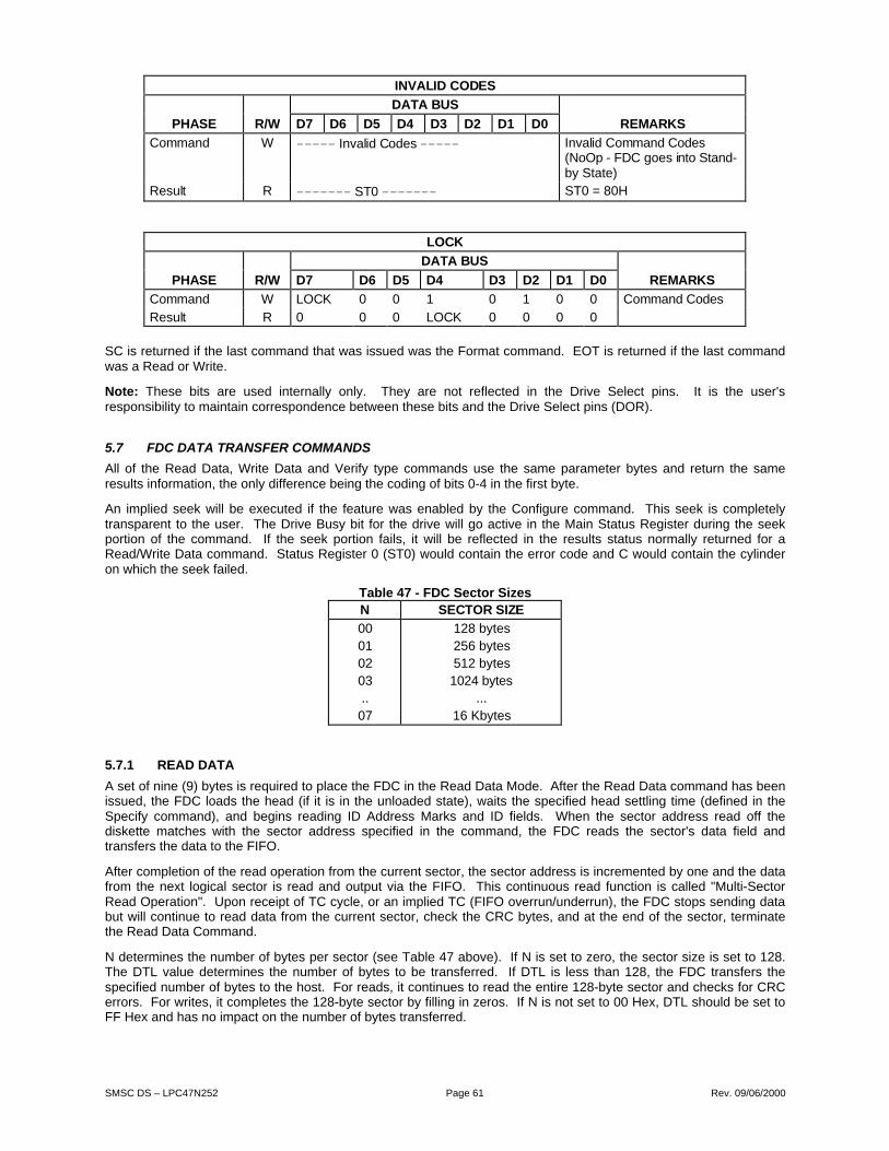
SMSC DS – LPC47N252 Page 61 Rev. 09/06/2000
INVAL ID COD ES
D AT A B US
PHA SE R /W D 7 D 6 D 5 D 4 D 3 D 2 D 1 D 0 R EM AR K S
C om mand W - -- -- Inval id C odes - -- -- Inval i d Com mand Codes( NoOp - FD C goes i nto Stand-by State)
R esul t R - -- -- - - ST 0 - -- -- - - ST0 = 80H
L OC K
D AT A B US
PHA SE R /W D 7 D 6 D 5 D 4 D 3 D 2 D 1 D 0 R EM AR K S
C om mand W LOC K 0 0 1 0 1 0 0 C om mand Codes
R esul t R 0 0 0 LOC K 0 0 0 0
SC is returned if the last command that was issued was the Format command. EOT is returned if the last commandwas a Read or Write.
Note: These bits are used internally only. They are not reflected in the Drive Select pins. It is the user'sresponsibility to maintain correspondence between these bits and the Drive Select pins (DOR).
5.7 FDC DATA TRANSFER COMMANDS
All of the Read Data, Write Data and Verify type commands use the same parameter bytes and return the sameresults information, the only difference being the coding of bits 0-4 in the first byte.
An implied seek will be executed if the feature was enabled by the Configure command. This seek is completelytransparent to the user. The Drive Busy bit for the drive will go active in the Main Status Register during the seekportion of the command. If the seek portion fails, it will be reflected in the results status normally returned for aRead/Write Data command. Status Register 0 (ST0) would contain the error code and C would contain the cylinderon which the seek failed.
Table 47 - FDC Sector SizesN SEC TOR SIZ E
00010203..07
128 bytes256 bytes512 bytes1024 bytes
...16 Kbytes
5.7.1 READ DATA
A set of nine (9) bytes is required to place the FDC in the Read Data Mode. After the Read Data command has beenissued, the FDC loads the head (if it is in the unloaded state), waits the specified head settling time (defined in theSpecify command), and begins reading ID Address Marks and ID fields. When the sector address read off thediskette matches with the sector address specified in the command, the FDC reads the sector's data field andtransfers the data to the FIFO.
After completion of the read operation from the current sector, the sector address is incremented by one and the datafrom the next logical sector is read and output via the FIFO. This continuous read function is called "Multi-SectorRead Operation". Upon receipt of TC cycle, or an implied TC (FIFO overrun/underrun), the FDC stops sending databut will continue to read data from the current sector, check the CRC bytes, and at the end of the sector, terminatethe Read Data Command.
N determines the number of bytes per sector (see Table 47 above). If N is set to zero, the sector size is set to 128.The DTL value determines the number of bytes to be transferred. If DTL is less than 128, the FDC transfers thespecified number of bytes to the host. For reads, it continues to read the entire 128-byte sector and checks for CRCerrors. For writes, it completes the 128-byte sector by filling in zeros. If N is not set to 00 Hex, DTL should be set toFF Hex and has no impact on the number of bytes transferred.

SMSC DS – LPC47N252 Page 62 Rev. 09/06/2000
The amount of data which can be handled with a single command to the FDC depends upon MT (multi-track) and N(number of bytes/sector).
The Multi-Track function (MT) allows the FDC to read data from both sides of the diskette. For a particular cylinder,data will be transferred starting at Sector 1, Side 0 and completing the last sector of the same track at Side 1.
If the host terminates a read or write operation in the FDC, the ID information in the result phase is dependent uponthe state of the MT bit and EOT byte.
At the completion of the Read Data command, the head is not unloaded until after the Head Unload Time Interval(specified in the Specify command) has elapsed. If the host issues another command before the head unloads, thenthe head settling time may be saved between subsequent reads.
If the FDC detects a pulse on the nINDEX pin twice without finding the specified sector (meaning that the diskette'sindex hole passes through index detect logic in the drive twice), the FDC sets the IC code in Status Register 0 to "01"indicating abnormal termination, sets the ND bit in Status Register 1 to "1" indicating a sector not found, andterminates the Read Data Command. After reading the ID and Data Fields in each sector, the FDC checks the CRCbytes. Ifa CRC error occurs in the ID or data field, the FDC sets the IC code in Status Register 0 to "01" indicatingabnormal termination, sets the DE bit flag in Status Register 1 to "1", sets the DD bit in Status Register 2 to "1" if CRCis incorrect in the ID field, and terminates the Read Data Command. Table 52 - Verify Command Result Phase Tabledescribes the effect of the SK bit on the Read Data command execution and results. Except where noted in Table48, the C or R value of the sector address is automatically incremented (see Table 54).
Table 48 - Effects Of MT and N Bits
M T N M AXIM U M TR A NSFER C APA CITY F IN AL SECT OR REA D FR OM DISK
0
101
01
1
122
33
256 x 26 = 6,656
256 x 52 = 13,312512 x 15 = 7,680512 x 30 = 15,360
1024 x 8 = 8,1921024 x 16 = 16,384
26 at si de 0 or 1
26 at si de 115 at si de 0 or 115 at si de 1
8 at side 0 or 116 at si de 1
Table 49 - Skip Bit vs Read Data Command
SK BIT VAL UE
D AT A A DD RESSM AR K T YPE
ENC OU N TERED R ESUL T S
SEC TOR R EA D?
C M BIT OFST2 SET? D ESCR IPT ION OF R ESUL T S
0 N or mal D ata Yes N o N or mal ter m inati on
0 D el eted Data Yes Yes Address not i ncr em ented. Nextsector not sear ched for
1 N or mal D ata Yes N o N or mal ter m inati on
1 D el eted Data N o Yes N or mal ter m inati on. Sector notr ead ( "ski pped" )
5.7.2 READ DELETED DATA
This command is the same as the Read Data command, only it operates on sectors that contain a Deleted DataAddress Mark at the beginning of a Data Field. Table 53 describes the effect of the SK bit on the Read Deleted Datacommand execution and results. Except where noted in Table 53, the C or R value of the sector address isautomatically incremented (See Table 54)
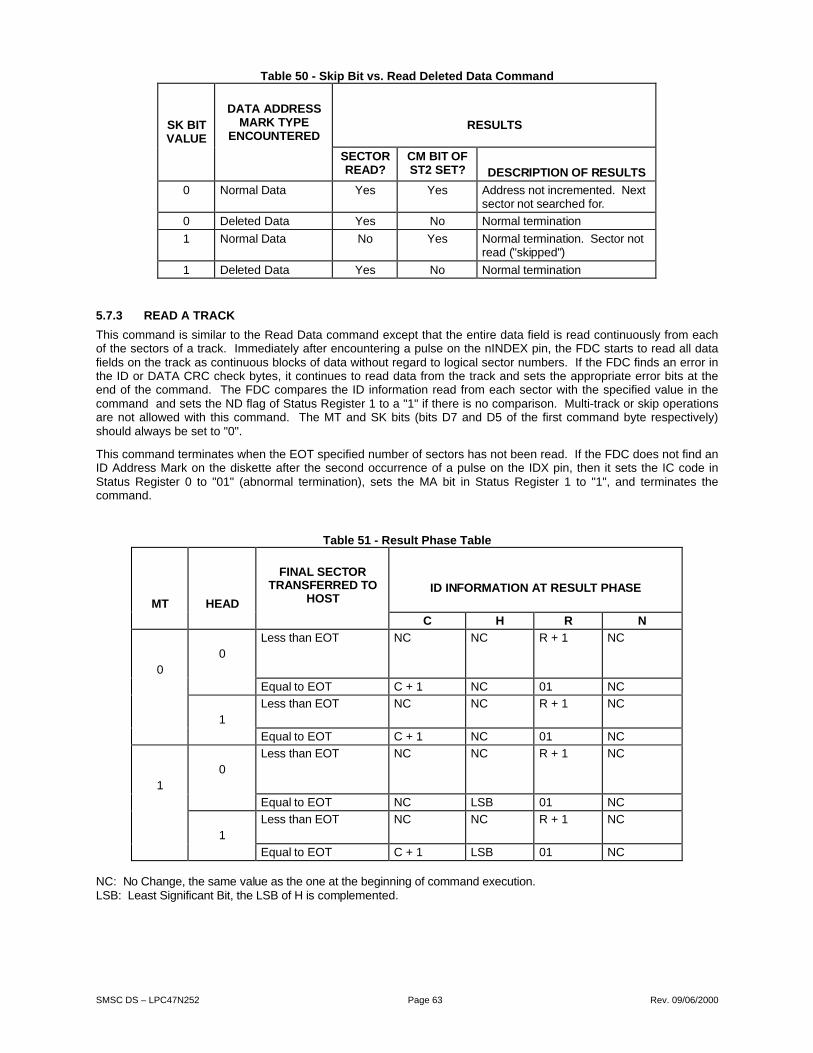
SMSC DS – LPC47N252 Page 63 Rev. 09/06/2000
Table 50 - Skip Bit vs. Read Deleted Data Command
SK BIT VAL UE
D AT A A DD RESSM AR K T YPE
ENC OU N TERED R ESUL T S
SEC TOR R EA D?
C M BIT OFST2 SET? D ESCR IPT ION OF R ESUL T S
0 N or mal D ata Yes Yes Address not i ncr em ented. Nextsector not sear ched for .
0 D el eted Data Yes N o N or mal ter m inati on
1 N or mal D ata N o Yes N or mal ter m inati on. Sector notr ead ( "ski pped" )
1 D el eted Data Yes N o N or mal ter m inati on
5.7.3 READ A TRACK
This command is similar to the Read Data command except that the entire data field is read continuously from eachof the sectors of a track. Immediately after encountering a pulse on the nINDEX pin, the FDC starts to read all datafields on the track as continuous blocks of data without regard to logical sector numbers. If the FDC finds an error inthe ID or DATA CRC check bytes, it continues to read data from the track and sets the appropriate error bits at theend of the command. The FDC compares the ID information read from each sector with the specified value in thecommand and sets the ND flag of Status Register 1 to a "1" if there is no comparison. Multi-track or skip operationsare not allowed with this command. The MT and SK bits (bits D7 and D5 of the first command byte respectively)should always be set to "0".
This command terminates when the EOT specified number of sectors has not been read. If the FDC does not find anID Address Mark on the diskette after the second occurrence of a pulse on the IDX pin, then it sets the IC code inStatus Register 0 to "01" (abnormal termination), sets the MA bit in Status Register 1 to "1", and terminates thecommand.
Table 51 - Result Phase Table
M T H EA D
F IN AL SECT ORT RA NSF ER RED T O
H OSTID IN F OR MA T ION A T RESUL T PHA SE
C H R N
00
Less than EOT N C N C R + 1 N C
Equal to EOT C + 1 N C 01 N C
1Less than EOT N C N C R + 1 N C
Equal to EOT C + 1 N C 01 N C
10
Less than EOT N C N C R + 1 N C
Equal to EOT N C LSB 01 N C
1Less than EOT N C N C R + 1 N C
Equal to EOT C + 1 LSB 01 N C
N C: N o Change, the sam e val ue as the one at the begi nni ng of com m and execution.LSB: Least Significant Bi t, the LSB of H i s com pl emented.
SMSC DS – LPC47N252 Page 64 Rev. 09/06/2000
5.7.4 WRITE DATA
After the Write Data command has been issued, the FDC loads the head (if it is in the unloaded state), waits thespecified head load time if unloaded (defined in the Specify command), and begins reading ID fields. When thesector address read from the diskette matches the sector address specified in the command, the FDC reads the datafrom the host via the FIFO and writes it to the sector's data field.
After writing data into the current sector, the FDC computes the CRC value and writes it into the CRC field at the endof the sector transfer. The Sector Number stored in "R" is incremented by one, and the FDC continues writing to thenext data field. The FDC continues this "Multi-Sector Write Operation". Upon receipt of a terminal count signal or if aFIFO over/under run occurs while a data field is being written, then the remainder of the data field is filled with zeros.
The FDC reads the ID field of each sector and checks the CRC bytes. If it detects a CRC error in one of the ID fields,it sets the IC code in Status Register 0 to "01" (abnormal termination), sets the DE bit of Status Register 1 to "1", andterminates the Write Data command.
The Write Data command operates in much the same manner as the Read Data command. The following items arethe same. Please refer to the Read Data Command for details:
Transfer Capacity
EN (End of Cylinder) bit
ND (No Data) bit
Head Load, Unload Time Interval
ID information when the host terminates the command
Definition of DTL when N = 0 and when N does not = 0
5.7.5 WRITE DELETED DATA
This command is almost the same as the Write Data command except that a Deleted Data Address Mark is written atthe beginning of the Data Field instead of the normal Data Address Mark. This command is typically used to mark abad sector containing an error on the floppy disk.
5.7.6 VERIFY
The Verify command is used to verify the data stored on a disk. This command acts exactly like a Read Datacommand except that no data is transferred to the host. Data is read from the disk and CRC is computed andchecked against the previously stored value.
Because data is not transferred to the host, TC cycle cannot be used to terminate this command. By setting the ECbit to "1", an implicit TC will be issued to the FDC. This implicit TC occur s when the SC value decrements to 0 (anSC value of 0 will verify 256 sectors). This command can also be terminated by setting the EC bit to "0" and the EOTvalue equal to the final sector to be checked. If EC is set to "0", DTL/SC should be programmed to 0FFH. Refer toTable 54 and Table 55 for information concerning the values of MT and EC versus SC and EOT value.
Definitions:
# Sectors Per Side = Number of formatted sectors per each side of the disk.
# Sectors Remaining = Number of formatted sectors left which can be read, including side 1 of the disk if MT is set to"1".

SMSC DS – LPC47N252 Page 65 Rev. 09/06/2000
Table 52 - Verify Command Result Phase TableM T EC SC/EOT VAL U E T ER MIN AT ION R ESU LT
0 0 SC = D TL
EOT ≤ # Sectors Per Side
Success Ter mi nationR esul t Phase Val id
0 0 SC = D TLEOT > # Sectors Per Side
U nsuccessful Ter mi nationR esul t Phase Inval id
0 1 SC ≤ # Sectors Remai ni ng AN D
EOT ≤ # Sectors Per Side
Successful Term i nati onR esul t Phase Val id
0 1 SC > # Sector s R em ai ning OREOT > # Sectors Per Side
U nsuccessful Ter mi nationR esul t Phase Inval id
1 0 SC = D TL
EOT ≤ # Sectors Per Side
Successful Term i nati onR esul t Phase Val id
1 0 SC = D TL
EOT > # Sectors Per Side
U nsuccessful Ter mi nation
R esul t Phase Inval id
1 1 SC ≤ # Sectors Remai ni ng AN D
EOT ≤ # Sectors Per Side
Successful Term i nati on
R esul t Phase Val id
1 1 SC > # Sector s R em ai ning OR
EOT > # Sectors Per Side
U nsuccessful Ter mi nation
R esul t Phase Inval id
Note: If MT is set to "1" and the SC value is greater than the number of remaining formatted sectors on Side 0,verifying will continue on Side 1 of the disk.
5.7.7 FORMAT A TRACK
The Format command allows an entire track to be formatted. After a pulse from the IDX pin is detected, the FDCstarts writing data on the disk including gaps, address marks, ID fields, and data fields per the IBM System 34 or3740 format (MFM or FM respectively). The particular values that will be written to the gap and data field arecontrolled by the values programmed into N, SC, GPL, and D which are specified by the host during the commandphase. The data field of the sector is filled with the data byte specified by D. The ID field for each sector is suppliedby the host; that is, four data bytes per sector are needed by the FDC for C, H, R, and N (cylinder, head, sectornumber and sector size respectively).
After formatting each sector, the host must send new values for C, H, R and N to the FDC for the next sector on thetrack. The R value (sector number) is the only value that must be changed by the host after each sector is formatted.This allows the disk to be formatted with nonsequential sector addresses (interleaving). This incrementing andformatting continues for the whole track until the FDC encounters a pulse on the IDX pin again and it terminates thecommand.
Table 57 contains typical values for gap fields which are dependent upon the size of the sector and the number ofsectors on each track. Actual values can vary due to drive electronics.

SMSC DS – LPC47N252 Page 66 Rev. 09/06/2000
Table 53 - Diskette Format Fields
SYSTEM 34 ( DOUB L E DEN SITY) F OR M AT
GAP4 a80x4E
SYN C 12x00
IAM GAP150x4E
SYN C 12x00
ID AM C YL
H D
SEC
N O
C R C
GAP222x4E
SYN C 12x00
D ATAAM
D AT A
C R C
GAP3
GAP4b
3xC 2
F C 3xA1
F E 3xA1
F BF 8
SYSTEM 3740 ( SIN GL E D EN SIT Y) F ORM AT
GAP4 a40xF F
SYN C 6x00
IAM GAP126xF F
SYN C 6x00
ID AM C YL
H D
SEC
N O
C R C
GAP211xF F
SYN C 6x00
D ATAAM
D AT A
C R C
GAP3
GAP4b
F C F E F B or F 8
PER PEN DICU L AR F ORM AT
GAP4 a80x4E
SYN C 12x00
IAM GAP150x4E
SYN C 12x00
ID AM C YL
H D
SEC
N O
C R C
GAP241x4E
SYN C 12x00
D ATAAM
D AT A
C R C
GAP3
GAP4b
3xC 2
F C 3xA1
F E 3xA1
F BF 8
Table 54 - Typical Values for FormattingF OR MA T SEC TOR SIZ E N SC GPL 1 GPL 2
5.25"D rives
F M
128128512102420484096...
000002030405...
121008040201
07101846C 8C 8
09193087F FF F
M FM
256256512*102420484096...
010102030405...
121009040201
0A202A80C 8C 8
0C3250F 0F FF F
3.5"D rives
F M128256512
012
0F0905
070F1B
1B2A3A
M FM 256512**1024
123
0F0905
0E1B35
365474
GPL 1 = suggested GPL val ues i n R ead and Wr ite com m ands to avoi d spl ice poi nt between data fi el dand ID fiel d of conti guous sections.
GPL 2 = suggested GPL val ue in Form at A T rack comm and. *PC /AT val ues ( typical)
**PS/2 val ues ( typical) . Appl i es w i th 1.0 MB and 2.0 M B dri ves.
N ot e: All values except sector size are in hex.

SMSC DS – LPC47N252 Page 67 Rev. 09/06/2000
5.8 FDC CONTROL COMMANDS
Control commands differ from the other commands in that no data transfer takes place. Three commands generatean interrupt when complete: Read ID, Recalibrate, and Seek. The other control commands do not generate aninterrupt.
5.8.1 READ ID
The Read ID command is used to find the present position of the recording heads. The FDC stores the values fromthe first ID field it is able to read into its registers. If the FDC does not find an ID address mark on the diskette afterthe second occurrence of a pulse on the nINDEX pin, it then sets the IC code in Status Register 0 to "01" (abnormaltermination), sets the MA bit in Status Register 1 to "1", and terminates the command.
The following commands will generate an interrupt upon completion. They do not return any result bytes. It is highlyrecommended that control commands be followed by the Sense Interrupt Status command. Otherwise, valuableinterrupt status information will be lost.
5.8.2 RECALIBRATE
This command causes the read/write head within the FDC to retract to the track 0 position. The FDC clears thecontents of the PCN counter and checks the status of the nTR0 pin from the FDD. As long as the nTR0 pin is low,the DIR pin remains 0 and step pulses are issued. When the nTR0 pin goes high, the SE bit in Status Register 0 isset to "1" and the command is terminated. If the nTR0 pin is still low after 79 step pulses have been issued, the FDCsets the SE and the EC bits of Status Register 0 to "1" and terminates the command. Disks capable of handling morethan 80 tracks per side may require more than one Recalibrate command to return the head back to physical Track 0.
The Recalibrate command does not have a result phase. The Sense Interrupt Status command must be issued afterthe Recalibrate command to effectively terminate it and to provide verification of the head position (PCN). During thecommand phase of the recalibrate operation, the FDC is in the BUSY state, but during the execution phase it is in aNON-BUSY state. At this time, another Recalibrate command may be issued, and in this manner parallel Recalibrateoperations may be done on up to four drives at once.
Upon power up, the software must issue a Recalibrate command to properly initialize all drives and the controller.
5.8.3 SEEK
The read/write head within the drive is moved from track to track under the control of the Seek command. The FDCcompares the PCN, which is the current head position, with the NCN and performs the following operation if there is adifference:
PCN < NCN:Direction signal to drive set to "1" (step in) and issues step pulses.
PCN > NCN:Direction signal to drive set to "0" (step out) and issues step pulses.
The rate at which step pulses are issued is controlled by SRT (Stepping Rate Time) in the Specify command. Aftereach step pulse is issued, NCN is compared against PCN, and when NCN = PCN the SE bit in Status Register 0 isset to "1" and the command is terminated.
During the command phase of the seek or recalibrate operation, the FDC is in the BUSY state, but during theexecution phase it is in the NON-BUSY state. At this time, another Seek or Recalibrate command may be issued,and in this manner, parallel seek operations may be done on up to four drives at once.
Note that if implied seek is not enabled, the read and write commands should be preceded by:
Seek command - Step to the proper track
Sense Interrupt Status command - Terminate the Seek command
Read ID - Verify head is on proper track
Issue Read/Write command.
The Seek command does not have a result phase. Therefore, it is highly recommended that the Sense InterruptStatus command be issued after the Seek command to terminate it and to provide verification of the head position(PCN). The H bit (Head Address) in ST0 will always return to a "0". When exiting POWERDOWN mode, the FDCclears the PCN value and the status information to zero. Prior to issuing the POWERDOWN command, it is highlyrecommended that the user service all pending interrupts through the Sense Interrupt Status command.

SMSC DS – LPC47N252 Page 68 Rev. 09/06/2000
5.8.4 SENSE INTERRUPT STATUS
An interrupt signal on the FDC is generated for one of the following reasons:
Upon entering the Result Phase of:
Read Data command
Read A Track command
Read ID command
Read Deleted Data command
Write Data command
Format A Track command
Write Deleted Data command
Verify command
End of Seek, Relative Seek, or Recalibrate command
FDC requires a data transfer during the execution phase in the non-DMA mode
The Sense Interrupt Status command resets the interrupt signal and, via the IC code and SE bit of Status Register 0,identifies the cause of the interrupt.
Table 55 - Interrupt IdentificationSE IC INT ER R UPT D UE T O
01
1
1100
01
Pol li ngN or mal ter m inati on of Seek orR ecal i br ate com m andAbnor m al term inati on of Seek or R ecal i br ate com m and
The Seek, Relative Seek, and Recalibrate commands have no result phase. The Sense Interrupt Status commandmust be issued immediately after these commands to terminate them and to provide verification of the head position(PCN). The H (Head Address) bit in ST0 will always return a "0". If a Sense Interrupt Status is not issued, the drivewill continue to be BUSY and may affect the operation of the next command.
5.8.5 SENSE DRIVE STATUS
Sense Drive Status obtains drive status information. It has no execution phase and goes directly to the result phasefrom the command phase. Status Register 3 contains the drive status information.
5.8.6 SPECIFY
The Specify command sets the initial values for each of the three internal times. The HUT (Head Unload Time)defines the time from the end of the execution phase of one of the read/write commands to the head unload state.The SRT (Step Rate Time) defines the time interval between adjacent step pulses. Note that the spacing betweenthe first and second step pulses may be shorter than the remaining step pulses. The HLT (Head Load Time) definesthe time between when the Head Load signal goes high and the read/write operation starts. The values change withthe data rate speed selection and are documented in Table 56 - Drive Control Delays (ms). The values are thesame for MFM and FM.
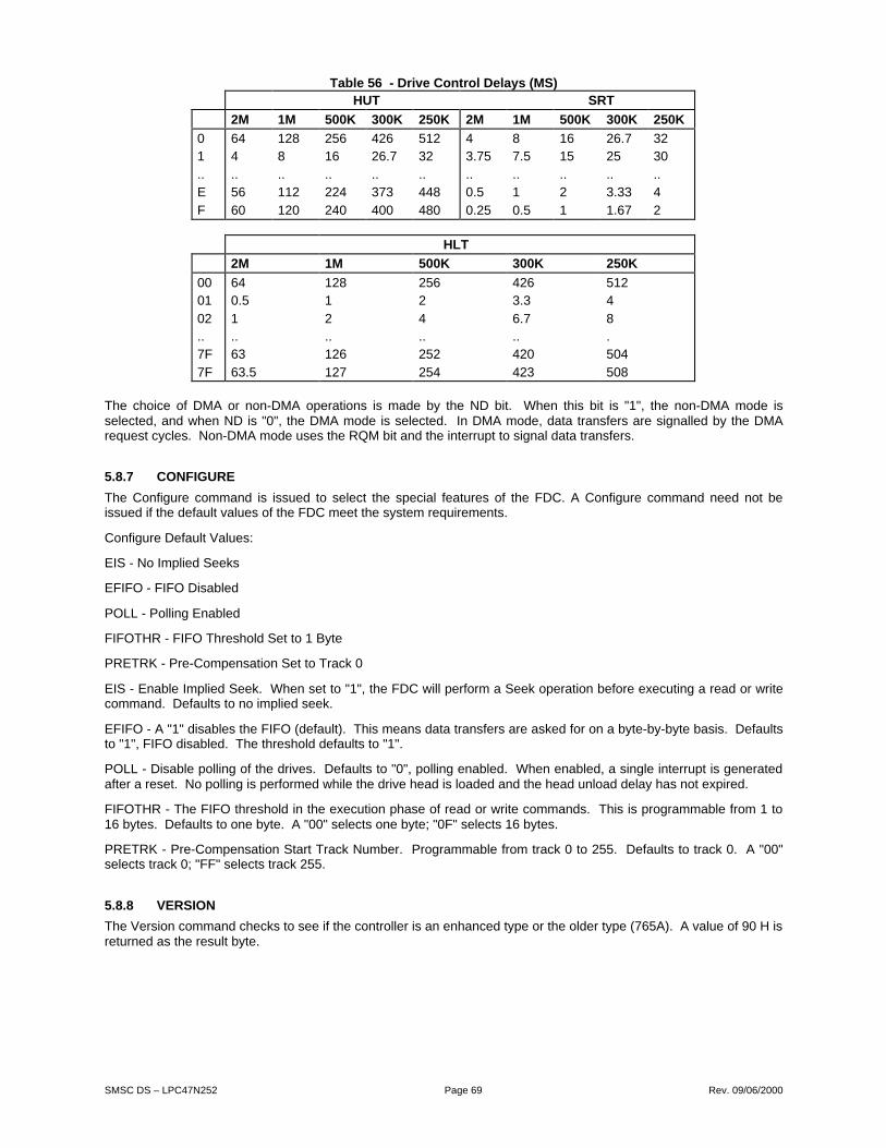
SMSC DS – LPC47N252 Page 69 Rev. 09/06/2000
Table 56 - Drive Control Delays (MS)H UT SRT
2M 1M 500K 300K 250K 2M 1M 500K 300K 250K
01
..E
F
644
..56
60
1288
..112
120
25616
..224
240
42626.7
..373
400
51232
..448
480
43.75
..0.5
0.25
87.5
..1
0.5
1615
..2
1
26.725
..3.33
1.67
3230
..4
2
H LT
2M 1M 500K 300K 250K
0001
02..7F
7F
640.5
1..63
63.5
1281
2..126
127
2562
4..252
254
4263.3
6.7..420
423
5124
8.504
508
The choice of DMA or non-DMA operations is made by the ND bit. When this bit is "1", the non-DMA mode isselected, and when ND is "0", the DMA mode is selected. In DMA mode, data transfers are signalled by the DMArequest cycles. Non-DMA mode uses the RQM bit and the interrupt to signal data transfers.
5.8.7 CONFIGURE
The Configure command is issued to select the special features of the FDC. A Configure command need not beissued if the default values of the FDC meet the system requirements.
Configure Default Values:
EIS - No Implied Seeks
EFIFO - FIFO Disabled
POLL - Polling Enabled
FIFOTHR - FIFO Threshold Set to 1 Byte
PRETRK - Pre-Compensation Set to Track 0
EIS - Enable Implied Seek. When set to "1", the FDC will perform a Seek operation before executing a read or writecommand. Defaults to no implied seek.
EFIFO - A "1" disables the FIFO (default). This means data transfers are asked for on a byte-by-byte basis. Defaultsto "1", FIFO disabled. The threshold defaults to "1".
POLL - Disable polling of the drives. Defaults to "0", polling enabled. When enabled, a single interrupt is generatedafter a reset. No polling is performed while the drive head is loaded and the head unload delay has not expired.
FIFOTHR - The FIFO threshold in the execution phase of read or write commands. This is programmable from 1 to16 bytes. Defaults to one byte. A "00" selects one byte; "0F" selects 16 bytes.
PRETRK - Pre-Compensation Start Track Number. Programmable from track 0 to 255. Defaults to track 0. A "00"selects track 0; "FF" selects track 255.
5.8.8 VERSION
The Version command checks to see if the controller is an enhanced type or the older type (765A). A value of 90 H isreturned as the result byte.

SMSC DS – LPC47N252 Page 70 Rev. 09/06/2000
5.8.9 RELATIVE SEEK
The command is coded the same as for Seek, except for the MSB of the first byte and the DIR bit.
D IR A CT ION
01
Step H ead OutStep H ead In
DIR Head Step Direction Control
RCN Relative Cylinder Number that determines how many tracks to step the head in or out from the current tracknumber.
The Relative Seek command differs from the Seek command in that it steps the head the absolute number of tracksspecified in the command instead of making a comparison against an internal register. The Seek command is goodfor drives that support a maximum of 256 tracks. Relative Seeks cannot be overlapped with other Relative Seeks.Only one Relative Seek can be active at a time. Relative Seeks may be overlapped with Seeks and Recalibrates. Bit4 of Status Register 0 (EC) will be set if Relative Seek attempts to step outward beyond Track 0.
As an example, assume that a floppy drive has 300 useable tracks. The host needs to read track 300 and the headis on any track (0-255). If a Seek command is issued, the head will stop at track 255. If a Relative Seek command isissued, the FDC will move the head the specified number of tracks, regardless of the internal cylinder positionregister (but will increment the register). If the head was on track 40 (d), the maximum track that the FDC couldposition the head on using Relative Seek will be 295 (D), the initial track + 255 (D). The maximum count that thehead can be moved with a single Relative Seek command is 255 (D).
The internal register, PCN, will overflow as the cylinder number crosses track 255 and will contain 39 (D). Theresulting PCN value is thus (RCN + PCN) mod 256. Functionally, the FDC starts counting from 0 again as the tracknumber goes above 255 (D). It is the user's responsibility to compensate FDC functions (precompensation tracknumber) when accessing tracks greater than 255. The FDC does not keep track that it is working in an "extendedtrack area" (greater than 255). Any command issued will use the current PCN value except for the Recalibratecommand, which only looks for the TRACK0 signal. Recalibrate will return an error if the head is farther than 79 dueto its limitation of issuing a maximum of 80 step pulses. The user simply needs to issue a second Recalibratecommand. The Seek command and implied seeks will function correctly within the 44 (D) track (299-255) area of the"extended track area". It is the user's responsibility not to issue a new track position that will exceed the maximumtrack that is present in the extended area.
To return to the standard floppy range (0-255) of tracks, a Relative Seek should be issued to cross the track 255boundary.
A Relative Seek can be used instead of the normal Seek, but the host is required to calculate the difference betweenthe current head location and the new (target) head location. This may require the host to issue a Read ID commandto ensure that the head is physically on the track that software assumes it to be. Different FDC commands will returndifferent cylinder results that may be difficult to keep track of with software without the Read ID command.
5.8.10 PERPENDICULAR MODE
The Perpendicular Mode command should be issued prior to executing Read/Write/Format commands that access adisk drive with perpendicular recording capability. With this command, the length of the Gap2 field and VCO enabletiming can be altered to accommodate the unique requirements of these drives.
Table 69 - UART Baud Rates, describes the effects of the WGATE and GAP bits for the Perpendicular Modecommand. Upon a reset, the FDC will default to the conventional mode (WGATE = 0, GAP = 0).
Selection of the 500 Kbps and 1 Mbps perpendicular modes is independent of the actual data rate selected in theData Rate Select Register. The user must ensure that these two data rates remain consistent.
The Gap2 and VCO timing requirements for perpendicular recording type drives are dictated by the design of theread/write head. In the design of this head, a pre-erase head precedes the normal read/write head by a distance of200 micrometers. This works out to about 38 bytes at a 1 Mbps recording density. Whenever the write head isenabled by the Write Gate signal, the pre-erase head is also activated at the same time. Thus, when the write head isinitially turned on, flux transitions recorded on the media for the first 38 bytes will not be preconditioned with the pre-erase head since it has not yet been activated. To accommodate this head activation and deactivation time, the

SMSC DS – LPC47N252 Page 71 Rev. 09/06/2000
Gap2 field is expanded to a length of 41 bytes. The format field illustrates the change in the Gap2 field size for theperpendicular format.
On the read back by the FDC, the controller must begin synchronization at the beginning of the sync field. For theconventional mode, the internal PLL VCO is enabled (VCOEN) approximately 24 bytes from the start of the Gap2field. But, when the controller operates in the 1 Mbps perpendicular mode (WGATE = 1, GAP = 1), VCOEN goesactive after 43 bytes to accommodate the increased Gap2 field size. For both cases, and approximate two-bytecushion is maintained from the beginning of the sync field for the purposes of avoiding write splices in the presence ofmotor speed variation.
For the Write Data case, the FDC activates Write Gate at the beginning of the sync field under the conventionalmode. The controller then writes a new sync field, data address mark, data field, and CRC. With the pre-erase headof the perpendicular drive, the write head must be activated in the Gap2 field to insure a proper write of the new syncfield. For the 1 Mbps perpendicular mode (WGATE = 1, GAP = 1), 38 bytes will be written in the Gap2 space. Sincethe bit density is proportional to the data rate, 19 bytes will be written in the Gap2 field for the 500 Kbps perpendicularmode (WGATE = 1, GAP =0). It should be noted that none of the alterations in Gap2 size, VCO timing, or WriteGate timing affect normal program flow. The information provided here is just for background purposes and is notneeded for normal operation. Once the Perpendicular Mode command is invoked, FDC software behavior from theuser standpoint is unchanged.
The perpendicular mode command is enhanced to allow specific drives to be designated Perpendicular recordingdrives. This enhancement allows data transfers between Conventional and Perpendicular drives without having toissue Perpendicular mode commands between the accesses of the different drive types, nor having to change writepre-compensation values.
When both GAP and WGATE bits of the PERPENDICULAR MODE COMMAND are both programmed to "0"(Conventional mode), then D0, D1, D2, D3, and D4 can be programmed independently to "1" for that drive to be setautomatically to Perpendicular mode. In this mode the following set of conditions also apply:
The GAP2 written to a perpendicular drive during a write operation will depend upon the programmed data rate.
The write pre-compensation given to a perpendicular mode drive will be 0ns.
For D0-D3 programmed to "0" for conventional mode drives any data written will be at the currently programmed writepre-compensation.
Note: Bits D0-D3 can only be overwritten when OW is programmed as a "1". If either GAP or WGATE is a "1" thenD0-D3 are ignored.
Software and hardware resets have the following effect on the PERPENDICULAR MODE COMMAND:
"Software" resets (via the DOR or DSR registers) will only clear GAP and WGATE bits to "0". D0-D3 are unaffectedand retain their previous value.
"Hardware" resets will clear all bits (GAP, WGATE and D0-D3) to "0", i.e all conventional mode.
Table 57 - Effects of WGATE and GAP Bits
W GA TE GAP M OD EL EN GT H OF GAP2
F OR MA T F IEL DPOR TION OF GA P 2 W RIT TEN B Y
W RITE DA TA OPER A TION
00
1
1
01
0
1
C onventi onalPer pendi cul ar
( 500 Kbps) R eser ved( Conventional )
Per pendi cul ar ( 1 Mbps)
22 Bytes22 Bytes
22 Bytes
41 Bytes
0 Bytes19 Bytes
0 Bytes
38 Bytes
5.8.11 LOCK
In order to protect systems with long DMA latencies against older application software that can disable the FIFO theLOCK Command has been added. This command should only be used by the FDC routines, and applicationsoftware should refrain from using it. If an application calls for the FIFO to be disabled then the CONFIGUREcommand should be used. The LOCK command defines whether the EFIFO, FIFOTHR, and PRETRK parameters ofthe CONFIGURE command can be RESET by the DOR and DSR registers. When the LOCK bit is set to logic "1" all

SMSC DS – LPC47N252 Page 72 Rev. 09/06/2000
subsequent "software RESETS by the DOR and DSR registers will not change the previously set parameters to theirdefault values. All "hardware" RESET from the RESET pin will set the LOCK bit to logic "0" and return the EFIFO,FIFOTHR, and PRETRK to their default values. A status byte is returned immediately after issuing a a LOCKcommand. This byte reflects the value of the LOCK bit set by the command byte.
5.8.12 ENHANCED DUMPREG
The DUMPREG command is designed to support system run-time diagnostics and application software developmentand debug. To accommodate the LOCK command and the enhanced PERPENDICULAR MODE command theeighth byte of the DUMPREG command contains the data from these two commands.
5.9 COMPATIBILITY
The LPC47N252 was designed with software compatibility in mind. It is a fully backwards- compatible solution withthe older generation 765A/B disk controllers. The FDC also implements on-board registers for compatibility with thePS/2, as well as PC/AT and PC/XT, FDC subsystems. After a hardware reset of the FDC, all registers, functions andenhancements default to a PC/AT, PS/2 or PS/2 Model 30 compatible operating mode, depending on how the IDENTand MFM bits are configured by the system BIOS.
5.9.1 PARALLEL PORT FDC
Refer to section 9.3.3, PPPI FDC Mode on page 112.
5.9.2 HOT SWAPPABLE FDD CAPABILITY
The FDC output pins will tri-state whenever the FDC Logical Device is powered-down or not activated. In additionsetting bit 7 of the FDD Mode Configuration register (LD0_CRF0) will tri-state the FDC output pins. Bit 7 only affectsthe standard FDC interface, it has no effect on the Parallel Port Floppy Interface.
The following table illustrates the state of the FDC and Parallel Port FDC pins for combinations of 1) the FDC OutputControl bit; 2) the Activate bit; and 3) the FDC powerdown state.
Table 58 - FDC Hot Swappong State Of The FDC And Parallel Port FDC Pins
FDD MODEREGISTER, BIT[7]
ACTIVATEBIT
FDC IN POWERDOWN FDC PINS
PARALLEL PORTFDC PINS
X 0 X Hi-Z Hi-Z
X 1 Y Hi-Z Hi-Z
0 1 N Active Active
1 1 N Hi-Z Active
When the FDC is disabled, powered down or inactive the FDC output pins will tri-state allowing ‘hot-swapping’ of theFloppy Disk Drive. The following table lists the five control/configuration mechanisms that power down or deactivatethe FDC logical device.
Table 59 - FDC Hot Swappong MechanismsMECHANISM FDC OUTPUT PINS STATE
Tri-State Tri-State Tri-State Tri-State
(Note 1)
Tri-State
(Note 2)
FDC Logical Dev Activate bit=0: FDC LD deactivated
=1: FDC LD activatedRefer to the description of the FDCLogical Device Configuration register0x30 in the Configuration section ofthe LPC47N252 Specification.
0 X 1 1 1

SMSC DS – LPC47N252 Page 73 Rev. 09/06/2000
MECHANISM FDC OUTPUT PINS STATE
FDC Logical Dev Base Address
0x100 < Base < 0x0FF8:FDC LD Base Address Valid.
0xFFF < Base < 0x100:FDC LD Base Address Invalid.
Refer to the description of the FDCBase I/O Address registers in theConfiguration section of theLPC47N252 Specification.
X INVALID
BASEADDRESS
VALID
BASEADDRESS
VALID
BASEADDRESS
VALID
BASEADDRESS
GCR 0x22 bit-0 (FDC Power)
=0: Power Off=1: Power OnRefer to the description of the GlobalConfig Register 0x22 in theConfiguration section of theLPC47N252 Specification.
X X 0 1 1
DSR, bit-6 (pwr down)=0: Normal Run
=1: Manual Pwr downRefer to the description of the DSRin the FDC section of any SMSCSuper or Ultra I/O data sheet.
X X X 1 0
GCR 0x23 bit-0 (FDC auto powermanagement)=1: Pwr Mngnt on=0: Pwr Mngnt off
Refer to the description of the GlobalConfig Register 0x23 in theConfiguration section of theLPC47N252 Specification.
X X X X 1
Note: FDC Output pins = nWDATA, DRVDEN0, nHDSELm nWGATE, nDIR, nSTEP, nDS1, nDS0, nMTR0,nMTR1.
Note 1: DSR pwr down overrides auto pwr down.
Note 2: Outputs tri-state only if all of the required auto power down conditions are met, otherwise outputs are active.See Auto Power Management Section of the FDC37C93x Data Sheet.
5.10 FDC FORCE WRITE PROTECT
The LPC47N252 includes a Force Write Protect function for the floppy disk controller. Force Write Protect assertsthe internal nWRTPRT input to the controller (Table 60 and FIGURE 7).

SMSC DS – LPC47N252 Page 74 Rev. 09/06/2000
nWRTPRT
FDC
nDS0
nDS1
nWRTPRT
nDS0
nDS1
FORCEWRTPRT
FIGURE 7 - FORCE WRITE PROTECT FUNCTION
Note: This figure is for illustration purposes only and is not intended to suggest specific implementation details.
The FORCE WRTPRT bit is D0 in the Disable register (see Section 11.8.3.1,Disable Register, on page 132.) TheFORCE WRTPRT bit is active-high and set to “0” by default. The Force Write Protect function applies to thenWRTPRT input from the FDD Interface as well as the nWRTPRT input from the Parallel Port FDC.
Table 60 - Force WRTPRT FunctionnWRTPRT(FDD PIN)
FORCEWRTPRT nDS0 nDS1
nWRTPRT(FDC) DESCRIPTION
0 X X X 0 Active nWRTPRT pin function isalways enabled.
1 1 1 1 1
1 0 1 1 1
nWRTPRT function inactive.
1 1 0 1 0
1 1 1 0 0
Enabled FORCE WRTPRT functionoverrides an inactive nWRTPRT pin.

SMSC DS – LPC47N252 Page 75 Rev. 09/06/2000
6 ACPI EMBEDDED CONTROLLER
ACPI defines a standard hardware and software communications interface between the OS and an embeddedcontroller. This interface allows the OS to support a standard driver that can directly communicate with the embeddedcontroller, allowing other drivers within the system to communicate with and use the EC resources; for example,Smart Battery and AML code (FIGURE 8).
The LPC47N252 contains an Embedded Controller Interface (ECI) to handle SCI Wake and Run-time eventprocessing (FIGURE 9). The ECI is configured in Logical Device Number 8 in the LPC47N252 configuration registermap and presents an 8042-style interface to the ISA host.
EC(Arbitrates Wake andRun-time SCI Events)
CHIPSET
GPEx
GPEy
Run-Time
Wake
(wake) Ring(run-time) Thermal(run-time) Dock
(wake & run-time) Battery
FIGURE 8 – EMBEDDED CONTROL (EC) ILLUSTRATION
EC InputBuffer
EC OutputBuffer
EC StatusRegister
SCIInterface
Code
MainFirmware
(8051)I/O
AC
PI
Inte
rfac
e
Run
-Tim
e
Wak
e
SCI Interface
Command Write
Data Write
Data Read
Status Read
FIGURE 9 – GENERIC ACPI EC BLOCK DIAGRAM
6.1 ECI CONFIGURATION REGISTERS
The three device configuration registers in LDN8 provide ECI activation control and the base address for the ECI run-time registers (Table 61). Register 0x30 is the Activate register. The Activate register qualifies address decoding forthe ECI; e.g., if the Activate bit D0 in the Activate register is “0”, ECI addresses will not be decoded; if the Activate bitis “1”, ECI addresses will be decoded depending on the values programmed in the ECI Primary Base Addressregisters. Registers 0x60 and 0x61 are the ECI Primary Base Address registers. Register 0x60 is the ECI PrimaryBase Address High Byte, register 0x61 is the ECI Primary Base Address Low Byte.
Note: Bits D0 and D2 in the ECI Primary Base Address Low Byte must be “0”. For example, 0x62 is a valid ECIBase Address, while 0x66 is not a valid ECI Base Address. The valid ECI Primary Base Address range is 0x0000 –0x0FFA.

SMSC DS – LPC47N252 Page 76 Rev. 09/06/2000
Table 61 – ECI Configuration Registers (LDN8)INDEX TYPE HARD
RESETSOFT
RESETVCC2POR
VCC1 &VCC0POR
DESCRIPTION
D7 D6 D5 D4 D3 D2 D1 D0
0x30 R/W 0x00 0x00 0x00 - ACTIVATE
Reserved Activate
0x60 R/W 0x00 0x00 0x00 - ECI PRIMARY BASE ADDRESS HIGH BYTE
“0” “0” “0” “0” A11 A10 A9 A8
0x61 R/W 0x62 0x62 0x62 - ECI PRIMARY BASE ADDRESS LOW BYTE1
A7 A6 A5 A4 A3 “0” A1 “0”
Note1: Bits D0 and D2 of the ECI Base Address Low Byte must be “0”.
6.2 ECI RUNTIME REGISTERS
An ACPI-compliant ECI contains three registers: EC_COMMAND, EC_STATUS, and EC_DATA. The ECI registersoccupy two addresses in the Host I/O space (Table 62).
The EC_DATA and EC_COMMAND registers appear as a single 8-bit data register in the 8051. The CMD bit in theEC_STATUS register is used by the 8051 to discriminate commands from data written by the host to the ECI. CMDis controlled by hardware: host writes to the EC_DATA register set CMD = “0”; host writes to the EC_COMMANDregister set CMD = “1”.
Descriptions of these registers follow in the sections below.
Table 62 – ECI Run-Time RegistersISA HOST INTERFACE 8051 INTERFACE
REGISTERNAME HOST INDEX
HOSTTYPE CMD1
8051INDEX(7F00+)
8051TYPE
POWERPLANE
VCC1POR
VCC2POR
EC_DATA ECI Base Address R/W 0 0x53 R/W VCC1 - -
EC_COMMAND ECI Base Address + 4 W 1 0x53 R VCC1 - -
EC_STATUS ECI Base Address + 4 R - 0x54 R/W VCC1 0x00 -Note1: CMD is bit D3 in the EC_STATUS register.
6.3 EC_STATUS REGISTER
The EC_STATUS register indicates the state of the Embedded Controller Interface. To the host, the EC_STATUSregister is read-only. To the 8051, some bits in the EC_STATUS register are read-only (Table 63). These bits arecontrolled by hardware. The 8051 software controlled bits in the EC_STATUS register are read/write.
Table 63 – EC_Status RegisterD7 D6 D5 D4 D3 D2 D1 D0
HOST TYPE R R R R R R R R
8051 TYPE R/W R/W R/W R/W R R/W R R
NAME UD1 SMI_EVT SCI_EVT BURST CMD UD1 IBF OBF
Note1: The UD bits are User-Defined. UD bits are maintained by 8051 software, only.
OBF Bit – D0The Output Buffer Full (OBF) flag is set when the 8051 writes a byte of data into the data port (EC_DATA), but thehost has not yet read it.
Once the host reads the status byte and sees the OBF flag set, the host reads the data port to get the byte of datathat the 8051 has written.

SMSC DS – LPC47N252 Page 77 Rev. 09/06/2000
Once the host reads the data, the OBF flag is automatically cleared by hardware. An EC_OBF interrupt signals the8051 that the data has been read by the host and the 8051 is free to write more data to the EC_DATA register.
The EC_OBF interrupt is generated whenever the OBF bit in the EC_STATUS register is reset. The EC_OBFinterrupt is routed to bit 3 in the INT0 SRC register (see Section 11.9.2 and
FIGURE 14 starting on page 136). The EC_OBF interrupt mask is bit 4 in the INT1 Mask register.
IBF Bit – D1The Input Buffer Full (IBF) flag is set when the host has written a byte of data to the command or data port, but the8051 has not yet read it.
An EC_IBF interrupt signals the 8051 that there is data available. Once the 8051 reads the status byte and sees theIBF flag set, the 8051 reads the data port to get the byte of data that the host has written.
Once the 8051 reads the data, the IBF flag is automatically cleared by hardware. The 8051 must then generate asoftware interrupt (SCI) to alert the host that the data has been read and that the host is free to write more data to theECI as needed.
An EC_IBF interrupt is generated whenever the IBF bit in the EC_STATUS register is set. The EC_IBF interrupt isrouted to bit 4 in the INT0 SRC register. The EC_IBF interrupt mask is bit 5 in the INT1 Mask register.
CMD Bit – D3The CMD bit is “1” when the EC_DATA register contains a command byte; the CMD bit is “0” when the EC_DATAregister contains a data byte.
The CMD bit is controlled by hardware: host writes to the EC_DATA register set CMD = “0”; host writes to theEC_COMMAND register set CMD = “1”.
The CMD bit allows the embedded controller to differentiate the start of a command sequence from a data byte writeoperation.
BURST Bit – D4The BURST bit is “1” when the EC is in Burst Mode for polled command processing; the BURST bit is “0” when theEC is in Normal Mode for interrupt-driven command processing.
The BURST bit is an 8051-maintained software flag that indicates the embedded controller has received the BurstEnable command from the host, has halted normal processing, and is waiting for a series of commands to be sentfrom the host. Burst Mode allows the OS or system management handler to quickly read and write several bytes ofdata at a time without the overhead of SCIs between commands.
Note: the BURST bit is maintained by 8051 software, only.
SCI_EVT Bit – D5The SCI Event flag SCI_EVT is “1” when an SCI event is pending; i.e., the 8051 is requesting an SCI query;SCI_EVT is “0” when no SCI events are pending.
The SCI_EVT bit is an 8051-maintained software flag that is set when the embedded controller has detected aninternal event that requires operating system attention. The EC sets SCI_EVT before generating an SCI to the OS.
Note: the SCI_EVT bit is maintained by 8051 software, only.
SMI_EVT Bit – D6The SMI Event flag SMI_EVT is “1” when an SMI event is pending; i.e., the 8051 is requesting an SMI query;SMI_EVT is “0” when no SMI events are pending.
The SMI_EVT bit is an 8051-maintained software flag that is set when the embedded controller has detected aninternal event that requires system management interrupt handler attention. The EC sets SMI_EVT beforegenerating an SMI.
Note: the SMI_EVT bit is maintained by 8051 software, only.
6.4 EC_COMMAND REGISTER
The EC_COMMAND register is a write-only register that allows the host to issue commands to the embeddedcontroller.

SMSC DS – LPC47N252 Page 78 Rev. 09/06/2000
Writes to the EC_COMMAND register are latched in the 8051 data register and the input buffer full flag is set in theEC_STATUS register. Writes to the EC_COMMAND register also cause the CMD bit to be set to “1” in theEC_STATUS register.
6.5 EC_DATA REGISTER
The EC_DATA register is a read/write register that allows the host to issue command arguments to the embeddedcontroller and allows the OS to read data returned by the embedded controller.
Host writes to the EC_DATA register are latched in the 8051 data register and the input buffer full flag is set in theEC_STATUS register. Host writes to the EC_DATA register also cause the CMD bit to be reset to “0” in theEC_STATUS register.
Host reads from the EC_DATA register return data from the 8051 data register and clear the output buffer full flag inthe EC_STATUS register.
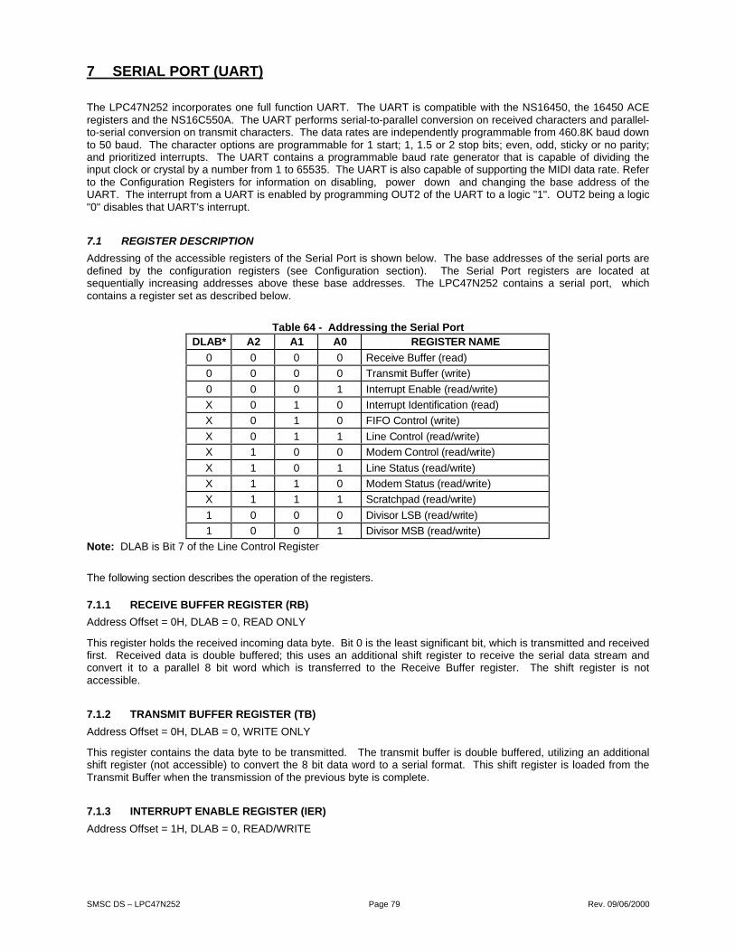
SMSC DS – LPC47N252 Page 79 Rev. 09/06/2000
7 SERIAL PORT (UART)
The LPC47N252 incorporates one full function UART. The UART is compatible with the NS16450, the 16450 ACEregisters and the NS16C550A. The UART performs serial-to-parallel conversion on received characters and parallel-to-serial conversion on transmit characters. The data rates are independently programmable from 460.8K baud downto 50 baud. The character options are programmable for 1 start; 1, 1.5 or 2 stop bits; even, odd, sticky or no parity;and prioritized interrupts. The UART contains a programmable baud rate generator that is capable of dividing theinput clock or crystal by a number from 1 to 65535. The UART is also capable of supporting the MIDI data rate. Referto the Configuration Registers for information on disabling, power down and changing the base address of theUART. The interrupt from a UART is enabled by programming OUT2 of the UART to a logic "1". OUT2 being a logic"0" disables that UART's interrupt.
7.1 REGISTER DESCRIPTION
Addressing of the accessible registers of the Serial Port is shown below. The base addresses of the serial ports aredefined by the configuration registers (see Configuration section). The Serial Port registers are located atsequentially increasing addresses above these base addresses. The LPC47N252 contains a serial port, whichcontains a register set as described below.
Table 64 - Addressing the Serial PortD LA B* A 2 A 1 A 0 R EGIST ER N A ME
0 0 0 0 R ecei ve Buffer ( read)
0 0 0 0 T ransm it Buffer (w ri te)
0 0 0 1 Inter r upt Enabl e ( read/wr i te)
X 0 1 0 Inter r upt Identi fi cation ( read)
X 0 1 0 F IF O C ontr ol (w r ite)
X 0 1 1 Line C ontr ol (r ead/w r ite)
X 1 0 0 M odem Contr ol ( r ead/w ri te)
X 1 0 1 Line Status ( read/wr i te)
X 1 1 0 M odem Status (r ead/w r ite)
X 1 1 1 Scr atchpad (r ead/w ri te)
1 0 0 0 D ivisor LSB ( read/wr i te)
1 0 0 1 D ivisor MSB ( read/wr i te)
Note: DLAB is Bit 7 of the Line Control Register
T he foll ow i ng section descri bes the oper ati on of the register s.
7.1.1 RECEIVE BUFFER REGISTER (RB)
Address Offset = 0H, DLAB = 0, READ ONLY
This register holds the received incoming data byte. Bit 0 is the least significant bit, which is transmitted and receivedfirst. Received data is double buffered; this uses an additional shift register to receive the serial data stream andconvert it to a parallel 8 bit word which is transferred to the Receive Buffer register. The shift register is notaccessible.
7.1.2 TRANSMIT BUFFER REGISTER (TB)
Address Offset = 0H, DLAB = 0, WRITE ONLY
This register contains the data byte to be transmitted. The transmit buffer is double buffered, utilizing an additionalshift register (not accessible) to convert the 8 bit data word to a serial format. This shift register is loaded from theTransmit Buffer when the transmission of the previous byte is complete.
7.1.3 INTERRUPT ENABLE REGISTER (IER)
Address Offset = 1H, DLAB = 0, READ/WRITE

SMSC DS – LPC47N252 Page 80 Rev. 09/06/2000
The lower four bits of this register control the enables of the five interrupt sources of the Serial Port interrupt. It ispossible to totally disable the interrupt system by resetting bits 0 through 3 of this register. Similarly, setting theappropriate bits of this register to a high, selected interrupts can be enabled. Disabling the interrupt system inhibitsthe Interrupt Identification Register and disables any Serial Port interrupt out of the LPC47N252 . All other systemfunctions operate in their normal manner, including the Line Status and MODEM Status Registers. The contents ofthe Interrupt Enable Register are described below.
BIT 0This bit enables the Received Data Available Interrupt (and timeout interrupts in the FIFO mode) when set to logic"1".
BIT 1This bit enables the Transmitter Holding Register Empty Interrupt when set to logic "1".
BIT 2This bit enables the Received Line Status Interrupt when set to logic "1". The error sources causing the interrupt areOverrun, Parity, Framing and Break. The Line Status Register must be read to determine the source.
BIT 3This bit enables the MODEM Status Interrupt when set to logic "1". This is caused when one of the Modem StatusRegister bits changes state.
BITS 4 - 7These bits are always logic "0".
7.1.4 FIFO CONTROL REGISTER (FCR)
Address Offset = 2H, DLAB = X, WRITE
This is a write only register at the same location as the IIR. This register is used to enable and clear the FIFOs, setthe RCVR FIFO trigger level. This write only register has a shadow register at MBX9Bh (see Table 204 – MailboxRegisters Interface on page 223.) Note: DMA is not supported.
BIT 0Setting this bit to a logic "1" enables both the XMIT and RCVR FIFOs. Clearing this bit to a logic "0" disables boththe XMIT and RCVR FIFOs and clears all bytes from both FIFOs. When changing from FIFO Mode to non-FIFO(16450) mode, data is automatically cleared from the FIFOs. This bit must be a 1 when other bits in this register arewritten to or they will not be properly programmed.
BIT 1Setting this bit to a logic "1" clears all bytes in the RCVR FIFO and resets its counter logic to “0”. The shift register isnot cleared. This bit is self-clearing.
BIT 2Setting this bit to a logic "1" clears all bytes in the XMIT FIFO and resets its counter logic to “0”. The shift register isnot cleared. This bit is self-clearing.
BIT 3Writing to this bit has no effect on the operation of the UART. The RXRDY and TXRDY pins are not available on thischip.
BITS 4 and 5Reserved
BITS 6 and 7These bits are used to set the trigger level for the RCVR FIFO interrupt.

SMSC DS – LPC47N252 Page 81 Rev. 09/06/2000
Table 65 - RCVR FIFO Trigger Level
B IT 7 B IT 6R CVR F IF O
T RIGGER LEVEL ( B YT ES) 0 0 10 1 41 0 81 1 14
7.1.5 INTERRUPT IDENTIFICATION REGISTER (IIR)
Address Offset = 2H, DLAB = X, READ
By accessing this register, the host CPU can determine the highest priority interrupt and its source. Four levels ofpriority interrupt exist. They are in descending order of priority:
Receiver Line Status (highest priority)
Received Data Ready
Transmitter Holding Register Empty
MODEM Status (lowest priority)
Information indicating that a prioritized interrupt is pending and the source of that interrupt is stored in the InterruptIdentification Register (refer to Interrupt Control Table). When the CPU accesses the IIR, the Serial Port freezes allinterrupts and indicates the highest priority pending interrupt to the CPU. During this CPU access, even if the SerialPort records new interrupts, the current indication does not change until access is completed. The contents of the IIRare described below.
BIT 0This bit can be used in either a hardwired prioritized or polled environment to indicate whether an interrupt is pending.When bit 0 is a logic "0", an interrupt is pending and the contents of the IIR may be used as a pointer to theappropriate internal service routine. When bit 0 is a logic "1", no interrupt is pending.
BITS 1 and 2These two bits of the IIR are used to identify the highest priority interrupt pending as indicated by Table 66 - InterruptControl Table.
BIT 3In non-FIFO mode, this bit is a logic "0". In FIFO mode this bit is set along with bit 2 when a timeout interrupt ispending.
BITS 4 and 5These bits of the IIR are always logic "0".
BITS 6 and 7These two bits are set when the FIFO CONTROL Register bit 0 equals 1.

SMSC DS – LPC47N252 Page 82 Rev. 09/06/2000
Table 66 - Interrupt Control TableF IF O
M OD EONL Y
INT ER R UPTIDENT IFICA T ION
R EGIST ER INT ER R UPT SET A N D RESET F U NC TIONS
B IT 3 B IT 2 B IT 1 B IT 0PRIOR ITY
L EVEL INT ER R UPT
T YPEINT ER R UPT
SOU RC EINT ER R UPT R ESET
C ON TR OL
0 0 0 1 - N one N one -
0 1 1 0 H ighest R ecei ver Li neStatus
Overr un Er r or ,Par ity Err or,F rami ng Er r or or Break Inter rupt
R eadi ng the Line StatusR egister
0 1 0 0 Second R ecei ved D ataAvail abl e
R ecei ver D ataAvail abl e
R ead R ecei ver Buffer or theF IF O drops below thetri gger level .
1 1 0 0 Second C haracterT im eoutIndicati on
N o CharactersH ave BeenR em oved Fr omor Input to theR CVR F IF Odur ing the last 4C har tim es andthere is at l east 1char i n it duri ngthi s tim e
R eadi ng the R eceiver Buffer R egi ster
0 0 1 0 T hi rd T ransm itter H ol di ng Register Empty
T ransm itter H ol di ng Register Empty
R eadi ng the IIR Regi ster ( ifSource of Inter r upt) or W ri ti ng the T ransm itter H ol di ng Register
0 0 0 0 F ourth M OD EM Status C lear to Send or D ata Set R eadyor Ri ng Indicatoror Data Car ri er D etect
R eadi ng the M OD EMStatus R egi ster
7.1.6 LINE CONTROL REGISTER (LCR)
Address Offset = 3H, DLAB = 0, READ/WRITE
Start LSB Data 5-8 bits MSB Parity Stop
This register contains the format information of the serial line. The bit definitions are:
BITS 0 and 1These two bits specify the number of bits in each transmitted or received serial character. The encoding of bits 0 and1 is as follows:

SMSC DS – LPC47N252 Page 83 Rev. 09/06/2000
Table 67 - Serial CharacterB IT 1 B IT 0 W OR D L EN GT H
0011
0101
5 Bits6 Bits7 Bits8 Bits
T he Star t, Stop and Par ity bits are not i ncluded i n the word length.
B IT 2T hi s bit specifi es the num ber of stop bi ts in each tr ansmi tted or recei ved ser ial char acter . T he fol lowi ng tablesum mar izes the i nfor m ation.
Table 68 - Stop Bits
B IT 2 W OR D L EN GT H N UM BER OFSTOP B IT S
0 - - 1
1 5 bits 1.5
1 6 bits 2
1 7 bits 2
1 8 bits 2
Note: The receiver will ignore all stop bits beyond the first, regardless of the number used in transmitting.
BIT 3Parity Enable bit. When bit 3 is a logic "1", a parity bit is generated (transmit data) or checked (receive data)between the last data word bit and the first stop bit of the serial data. (The parity bit is used to generate an even orodd number of 1s when the data word bits and the parity bit are summed).
BIT 4Even Parity Select bit. When bit 3 is a logic "1" and bit 4 is a logic "0", an odd number of logic "1"'s is transmitted orchecked in the data word bits and the parity bit. When bit 3 is a logic "1" and bit 4 is a logic "1" an even number ofbits is transmitted and checked.
BIT 5Stick Parity bit. When parity is enabled it is used in conjunction with bit 4 to select Mark or Space Parity. When LCRbits 3, 4 and 5 are 1 the Parity bit is transmitted and checked as a 0 (Space Parity). If bits 3 and 5 are 1 and bit 4 is a0, then the Parity bit is transmitted and checked as 1 (Mark Parity). If bit 5 is 0 Stick Parity is disabled. Bit 3 is a logic"1" and bit 5 is a logic "1", the parity bit is transmitted and then detected by the receiver in the opposite state indicatedby bit 4.
BIT 6Set Break Control bit. When bit 6 is a logic "1", the transmit data output (TXD) is forced to the Spacing or logic "0"state and remains there (until reset by a low level bit 6) regardless of other transmitter activity. This feature enablesthe Serial Port to alert a terminal in a communications system.
BIT 7Divisor Latch Access Bit (DLAB). It must be set high (logic "1") to access the Divisor Latches of the Baud RateGenerator during read or write operations. It must be set low (logic "0") to access the Receiver Buffer Register, theTransmitter Holding Register, or the Interrupt Enable Register.
7.1.7 MODEM CONTROL REGISTER (MCR)
Address Offset = 4H, DLAB = X, READ/WRITE
This 8 bit register controls the interface with the MODEM or data set (or device emulating a MODEM). The contentsof the MODEM control register are described below.
BIT 0This bit controls the Data Terminal Ready (nDTR) output. When bit 0 is set to a logic "1", the nDTR output is forcedto a logic "0". When bit 0 is a logic "0", the nDTR output is forced to a logic "1".

SMSC DS – LPC47N252 Page 84 Rev. 09/06/2000
BIT 1This bit controls the Request To Send (nRTS) output. Bit 1 affects the nRTS output in a manner identical to thatdescribed above for bit 0.
BIT 2This bit controls the Output 1 (OUT1) bit. This bit does not have an output pin and can only be read or written by theCPU.
BIT 3Output 2 (OUT2). This bit is used to enable an UART interrupt. When OUT2 is a logic "0", the serial port interruptoutput is forced to a high impedance state - disabled. When OUT2 is a logic "1", the serial port interrupt outputs areenabled.
BIT 4This bit provides the loopback feature for diagnostic testing of the Serial Port. When bit 4 is set to logic "1", thefollowing occur:
The TXD is set to the Marking State(logic "1").
The receiver Serial Input (RXD) is disconnected.
The output of the Transmitter Shift Register is "looped back" into the Receiver Shift Register input.
All MODEM Control inputs (nCTS, nDSR, nRI and nDCD) are disconnected.
The four MODEM Control outputs (nDTR, nRTS, OUT1 and OUT2) are internally connected to the four MODEMControl inputs (nDSR, nCTS, RI, DCD).
The Modem Control output pins are forced inactive high.
Data that is transmitted is immediately received.
This feature allows the processor to verify the transmit and receive data paths of the Serial Port. In the diagnosticmode, the receiver and the transmitter interrupts are fully operational. The MODEM Control Interrupts are alsooperational but the interrupts' sources are now the lower four bits of the MODEM Control Register instead of theMODEM Control inputs. The interrupts are still controlled by the Interrupt Enable Register.
BITS 5 - 7These bits are permanently set to logic zero.
7.1.8 LINE STATUS REGISTER (LSR)
Address Offset = 5H, DLAB = X, READ/WRITE
BIT 0Data Ready (DR). It is set to a logic "1" whenever a complete incoming character has been received and transferredinto the Receiver Buffer Register or the FIFO. Bit 0 is reset to a logic "0" by reading all of the data in the ReceiveBuffer Register or the FIFO.
BIT 1Overrun Error (OE). Bit 1 indicates that data in the Receiver Buffer Register was not read before the next characterwas transferred into the register, thereby destroying the previous character. In FIFO mode, an overrun error willoccur only when the FIFO is full and the next character has been completely received in the shift register, thecharacter in the shift register is overwritten but not transferred to the FIFO. The OE indicator is set to a logic "1"immediately upon detection of an overrun condition, and reset whenever the Line Status Register is read.
BIT 2Parity Error (PE). Bit 2 indicates that the received data character does not have the correct even or odd parity, asselected by the even parity select bit. The PE is set to a logic "1" upon detection of a parity error and is reset to alogic "0" whenever the Line Status Register is read. In the FIFO mode this error is associated with the particularcharacter in the FIFO it applies to. This error is indicated when the associated character is at the top of the FIFO.
SMSC DS – LPC47N252 Page 85 Rev. 09/06/2000
BIT 3Framing Error (FE). Bit 3 indicates that the received character did not have a valid stop bit. Bit 3 is set to a logic "1"whenever the stop bit following the last data bit or parity bit is detected as a zero bit (Spacing level). The FE is resetto a logic "0" whenever the Line Status Register is read. In the FIFO mode this error is associated with the particularcharacter in the FIFO it applies to. This error is indicated when the associated character is at the top of the FIFO.The Serial Port will try to resynchronize after a framing error. To do this, it assumes that the framing error was due tothe next start bit, so it samples this 'start' bit twice and then takes in the 'data'.
BIT 4Break Interrupt (BI). Bit 4 is set to a logic "1" whenever the received data input is held in the Spacing state (logic "0")for longer than a full word transmission time (that is, the total time of the start bit + data bits + parity bits + stop bits).The BI is reset after the CPU reads the contents of the Line Status Register. In the FIFO mode this error isassociated with the particular character in the FIFO it applies to. This error is indicated when the associatedcharacter is at the top of the FIFO. When break occurs only one zero character is loaded into the FIFO. Restartingafter a break is received, requires the serial data (RXD) to be logic "1" for at least 1/2 bit time. Note: Bits 1 through 4are the error conditions that produce a Receiver Line Status Interrupt whenever any of the corresponding conditionsare detected and the interrupt is enabled.
BIT 5Transmitter Holding Register Empty (THRE). Bit 5 indicates that the Serial Port is ready to accept a new characterfor transmission. In addition, this bit causes the Serial Port to issue an interrupt when the Transmitter HoldingRegister interrupt enable is set high. The THRE bit is set to a logic "1" when a character is transferred from theTransmitter Holding Register into the Transmitter Shift Register. The bit is reset to logic "0" whenever the CPU loadsthe Transmitter Holding Register. In the FIFO mode this bit is set when the XMIT FIFO is empty, it is cleared when atleast 1 byte is written to the XMIT FIFO. Bit 5 is a read only bit.
BIT 6Transmitter Empty (TEMT). Bit 6 is set to a logic "1" whenever the Transmitter Holding Register (THR) andTransmitter Shift Register (TSR) are both empty. It is reset to logic "0" whenever either the THR or TSR contains adata character. Bit 6 is a read only bit. In the FIFO mode this bit is set whenever the THR and TSR are both empty,
BIT 7This bit is permanently set to logic "0" in the 450 mode. In the FIFO mode, this bit is set to a logic "1" when there is atleast one parity error, framing error or break indication in the FIFO. This bit is cleared when the LSR is read if thereare no subsequent errors in the FIFO.
7.1.9 MODEM STATUS REGISTER (MSR)
Address Offset = 6H, DLAB = X, READ/WRITE This 8 bit register provides the current state of the control lines fromthe MODEM (or peripheral device). In addition to this current state information, four bits of the MODEM StatusRegister (MSR) provide change information.
These bits are set to logic "1" whenever a control input from the MODEM changes state. They are reset to logic"0" whenever the MODEM Status Register is read.
BIT 0Delta Clear To Send (DCTS). Bit 0 indicates that the nCTS input to the chip has changed state since the last time theMSR was read.
BIT 1Delta Data Set Ready (DDSR). Bit 1 indicates that the nDSR input has changed state since the last time the MSRwas read.
BIT 2Trailing Edge of Ring Indicator (TERI). Bit 2 indicates that the nRI input has changed from logic "0" to logic "1".
BIT 3Delta Data Carrier Detect (DDCD). Bit 3 indicates that the nDCD input to the chip has changed state.
Note: Whenever bit 0, 1, 2, or 3 is set to a logic "1", a MODEM Status Interrupt is generated.

SMSC DS – LPC47N252 Page 86 Rev. 09/06/2000
BIT 4This bit is the complement of the Clear To Send (nCTS) input. If bit 4 of the MCR is set to logic "1", this bit isequivalent to nRTS in the MCR.
BIT 5This bit is the complement of the Data Set Ready (nDSR) input. If bit 4 of the MCR is set to logic "1", this bit isequivalent to DTR in the MCR.
BIT 6This bit is the complement of the Ring Indicator (nRI) input. If bit 4 of the MCR is set to logic "1", this bit is equivalentto OUT1 in the MCR.
BIT 7This bit is the complement of the Data Carrier Detect (nDCD) input. If bit 4 of the MCR is set to logic "1", this bit isequivalent to OUT2 in the MCR.
7.1.10 SCRATCHPAD REGISTER (SCR)
Address Offset =7H, DLAB =X, READ/WRITE
This 8 bit read/write register has no effect on the operation of the Serial Port. It is intended as a scratchpad registerto be used by the programmer to hold data temporarily.
7.1.11 PROGRAMMABLE BAUD RATE GENERATOR (AND DIVISOR LATCHES DLH, DLL)
The Serial Port contains a programmable Baud Rate Generator that is capable of dividing the internal PLL clock byany divisor from 1 to 65535. The internal PLL clock is divided down to generate a 1.8462MHz frequency for BaudRates less than 38.4k, a 1.8432MHz frequency for 115.2k, a 3.6864MHz frequency for 230.4k and a 7.3728MHzfrequency for 460.8k.This output frequency of the Baud Rate Generator is 16x the Baud rate. Two 8 bit latches storethe divisor in 16 bit binary format. These Divisor Latches must be loaded during initialization in order to insuredesired operation of the Baud Rate Generator. Upon loading either of the Divisor Latches, a 16 bit Baud counter isimmediately loaded. This prevents long counts on initial load. If a 0 is loaded into the BRG registers the outputdivides the clock by the number 3. If a 1 is loaded the output is the inverse of the input oscillator. If a two is loadedthe output is a divide by 2 signal with a 50% duty cycle. If a 3 or greater is loaded the output is low for 2 bits and highfor the remainder of the count. The input clock to the BRG is a 1.8462 MHz clock.
Table 69 show s the baud rates possible.

SMSC DS – LPC47N252 Page 87 Rev. 09/06/2000
Table 69 - UART Baud RatesD ESIR ED
B AU D R AT E
D IVISOR USED TOGEN ER A TE 16X CL OCK
PER CEN T ER R OR D IFF ER ENC EB ET WEEN DESIR ED AN D A CT UA L 1
H IGHSPEED BIT2
50 2304 0.1 X
75 1536 - X
110 1047 - X
134.5 857 0.4 X
150 768 - X
300 384 - X
600 192 - X
1200 96 - X
1800 64 - X
2000 58 0.5 X
2400 48 - X
3600 32 - X
4800 24 - X
7200 16 - X
9600 12 - X
19200 6 - X
38400 3 - X
57600 2 0.16 X
115200 1 0.16 X
230400 32770 0.16 1
460800 32769 0.16 1Note1: The percentage error for all baud rates, except where indicated otherwise, is 0.2%.
Baud RatesNote2: The High Speed bit is located in the Device Configuration Space.Using 1.8462 MHz Clock for Baud Rate <= 57.6K;Using 1.8432 MHz Clock forBaud Rate = 115.2k;Using 3.6864 MHz Clock forBaud Rate = 230.4k;Using 7.3728 MHz Clock forBaud Rate = 460.8k
7.2 FIFO INTERRUPT MODE OPERATION
When the RCVR FIFO and receiver interrupts are enabled (FCR bit 0 = "1", IER bit 0 = "1"), RCVR interrupts occur asfollows:
The receive data available interrupt will be issued when the FIFO has reached its programmed trigger level; it iscleared as soon as the FIFO drops below its programmed trigger level.
The IIR receive data available indication also occurs when the FIFO trigger level is reached. It is cleared when theFIFO drops below the trigger level.
The receiver line status interrupt (IIR=06H), has higher priority than the received data available (IIR=04H) interrupt.
The data ready bit (LSR bit 0) is set as soon as a character is transferred from the shift register to the RCVR FIFO. Itis reset when the FIFO is empty.
When RCVR FIFO and receiver interrupts are enabled, RCVR FIFO timeout interrupts occur as follows:
A FIFO timeout interrupt occurs if all the following conditions exist:
at least one character is in the FIFO
The most recent serial character received was longer than 4 continuous character times ago. (If 2 stop bits areprogrammed, the second one is included in this time delay.)
The most recent CPU read of the FIFO was longer than 4 continuous character times ago.

SMSC DS – LPC47N252 Page 88 Rev. 09/06/2000
This will cause a maximum character received to interrupt issued delay of 160 msec at 300 BAUD with a 12 bitcharacter.
Character times are calculated by using the RCLK input for a clock signal (this makes the delay proportional to thebaudrate).
When a timeout interrupt has occurred it is cleared and the timer reset when the CPU reads one character from theRCVR FIFO.
When a timeout interrupt has not occurred the timeout timer is reset after a new character is received or after theCPU reads the RCVR FIFO.
When the XMIT FIFO and transmitter interrupts are enabled (FCR bit 0 = "1", IER bit 1 = "1"), XMIT interrupts occuras follows:
The transmitter holding register interrupt (02H) occurs when the XMIT FIFO is empty; it is cleared as soon as thetransmitter holding register is written to (1 of 16 characters may be written to the XMIT FIFO while servicing thisinterrupt) or the IIR is read.
The transmitter FIFO empty indications will be delayed 1 character time minus the last stop bit time whenever thefollowing occurs: THRE=1 and there have not been at least two bytes at the same time in the transmitter FIFO sincethe last THRE=1. The transmitter interrupt after changing FCR0 will be immediate, if it is enabled.
Character timeout and RCVR FIFO trigger level interrupts have the same priority as the current received dataavailable interrupt; XMIT FIFO empty has the same priority as the current transmitter holding register empty interrupt.
7.3 FIFO POLLED MODE OPERATION
With FCR bit 0 = "1" resetting IER bits 0, 1, 2 or 3 or all to zero puts the UART in the FIFO Polled Mode of operation.Since the RCVR and XMITTER are controlled separately, either one or both can be in the polled mode of operation.
In this mode, the user's program will check RCVR and XMITTER status via the LSR. LSR definitions for the FIFOPolled Mode are as follows:
Bit 0=1 as long as there is one byte in the RCVR FIFO.
Bits 1 to 4 specify which error(s) have occurred. Character error status is handled the same way as when in theinterrupt mode, the IIR is not affected since EIR bit 2=0.
Bit 5 indicates when the XMIT FIFO is empty.
Bit 6 indicates that both the XMIT FIFO and shift register are empty.
Bit 7 indicates whether there are any errors in the RCVR FIFO.
There is no trigger level reached or timeout condition indicated in the FIFO Polled Mode, however, the RCVR andXMIT FIFOs are still fully capable of holding characters.

SMSC DS – LPC47N252 Page 89 Rev. 09/06/2000
7.3.1 EFFECT OF THE RESET ON REGISTER FILE
The Reset Function Table (Table 70) details the effect of Vcc2 POR or nRESET_OUT on each of the registers of theSerial Port.
Table 70 - Reset Function TableR EGIST ER /SIGN AL R ESET CONT R OL R ESET ST AT E
Inter r upt Enabl e R egi ster R ESET All bi ts l ow
Inter r upt Identi fi cation R eg. R ESET Bit 0 is hi gh; Bits 1 - 7 low
F IF O C ontr ol R ESET All bi ts l ow
Line C ontr ol Reg. R ESET All bi ts l ow
M OD EM Contr ol R eg. R ESET All bi ts l ow
Line Status R eg. R ESET All bi ts l ow except 5, 6 high
M OD EM Status Reg. R ESET Bits 0 - 3 low; Bi ts 4 - 7 i nput
T XD 1, TXD2 R ESET H igh
INT RPT ( RC VR er r s) R ESET /Read LSR Low
INT RPT ( RC VR Data Ready) R ESET /Read RBR Low
INT RPT ( TH R E) R ESET /ReadIIR /W r ite T HR Low
OUT 2B R ESET H igh
R TSB R ESET H igh
D TR B R ESET H igh
OUT 1B R ESET H igh
R CVR F IF O R ESET /F CR 1*F CR 0/_FC R0
All Bi ts Low
XMIT F IF O R ESET /F CR 1*F CR 0/_FC R0
All Bi ts Low

SMSC DS – LPC47N252 Page 90 Rev. 09/06/2000
Table 71 - Register Summary for an Individual UART Channel
REGISTERADDRESS*
REGISTERNAME
REGISTERSYMBOL BIT 0 BIT 1 BIT 2 BIT 3 BIT 4 BIT 5 BIT 6 BIT 7
ADDR = 0
DLAB = 0
Receive BufferRegister (ReadOnly)
RBR Data Bit 0
(Note 1)
Data Bit 1 Data Bit 2 Data Bit 3 Data Bit 4 Data Bit 5 Data Bit 6 Data Bit 7
ADDR = 0
DLAB = 0
TransmitterHolding Register(Write Only)
THR Data Bit 0 Data Bit 1 Data Bit 2 Data Bit 3 Data Bit 4 Data Bit 5 Data Bit 6 Data Bit 7
ADDR = 1
DLAB = 0
Interrupt EnableRegister
IER EnableReceivedDataAvailableInterrupt(ERDAI)
EnableTransmitterHoldingRegisterEmptyInterrupt(ETHREI)
EnableReceiverLineStatusInterrupt(ELSI)
EnableMODEMStatusInterrupt(EMSI)
0 0 0 0
ADDR = 2 Interrupt Ident.Register (ReadOnly)
IIR "0" ifInterruptPending
Interrupt IDBit
InterruptID Bit
Interrupt IDBit (Note 5)
0 0 FIFOsEnabled
(Note 5)
FIFOsEnabled(Note 5)
ADDR = 2 FIFO ControlRegister (WriteOnly)
FCR
(Note 7)
FIFOEnable
RCVR FIFOReset
XMITFIFOReset
DMA ModeSelect (Note6)
Reserved Reserved RCVRTrigger LSB
RCVRTriggerMSB
ADDR = 3 Line ControlRegister
LCR WordLengthSelect Bit 0(WLS0)
WordLengthSelect Bit 1(WLS1)
Number ofStop Bits(STB)
ParityEnable(PEN)
Even ParitySelect (EPS)
Stick Parity Set Break DivisorLatchAccess Bit(DLAB)
ADDR = 4 MODEM ControlRegister
MCR DataTerminalReady(DTR)
Request toSend (RTS)
OUT1
(Note 3)
OUT2
(Note 3)
Loop 0 0 0
ADDR = 5 Line StatusRegister
LSR DataReady(DR)
OverrunError (OE)
ParityError (PE)
FramingError (FE)
BreakInterrupt (BI)
TransmitterHoldingRegister(THRE)
TransmitterEmpty(TEMT)(Note 2)
Error inRCVRFIFO (Note5)
ADDR = 6 MODEM StatusRegister
MSR Delta Clearto Send(DCTS)
Delta DataSet Ready(DDSR)
TrailingEdge RingIndicator(TERI)
Delta DataCarrierDetect(DDCD)
Clear to Send(CTS)
Data SetReady(DSR)
RingIndicator(RI)
DataCarrierDetect(DCD)
ADDR = 7 Scratch Register(Note 4)
SCR Bit 0 Bit 1 Bit 2 Bit 3 Bit 4 Bit 5 Bit 6 Bit 7
ADDR = 0
DLAB = 1
Divisor Latch(LS)
DDL Bit 0 Bit 1 Bit 2 Bit 3 Bit 4 Bit 5 Bit 6 Bit 7
ADDR = 1
DLAB = 1
Divisor Latch(MS)
DLM Bit 8 Bit 9 Bit 10 Bit 11 Bit 12 Bit 13 Bit 14 Bit 15
UART Register Summary Notes:
*DLAB is Bit 7 of the Line Control Register (ADDR = 3).
Note 1: Bit 0 is the least significant bit. It is the first bit serially transmitted or received.
Note 2: When operating in the XT mode, this bit will be set any time that the transmitter shift register is empty.
Note 3: This bit no longer has a pin associated with it.
Note 4: When operating in the XT mode, this register is not available.
Note 5: These bits are always zero in the non-FIFO mode.
Note 6: Writing a one to this bit has no effect. DMA modes are not supported in this chip.
7.3.2 NOTES ON SERIAL PORT FIFO MODE OPERATION
The RCVR FIFO will hold up to 16 bytes regardless of which trigger level is selected.
7.3.3 TX AND RX FIFO OPERATION
The Tx portion of the UART transmits data through TXD as soon as the CPU loads a byte into the Tx FIFO. TheUART will prevent loads to the Tx FIFO if it currently holds 16 characters. Loading to the Tx FIFO will again beenabled as soon as the next character is transferred to the Tx shift register. These capabilities account for the largelyautonomous operation of the Tx.
The UART starts the above operations typically with a Tx interrupt. The chip issues a Tx interrupt whenever the TxFIFO is empty and the Tx interrupt is enabled, except in the following instance. Assume that the Tx FIFO is empty
SMSC DS – LPC47N252 Page 91 Rev. 09/06/2000
and the CPU starts to load it. When the first byte enters the FIFO the Tx FIFO empty interrupt will transition fromactive to inactive. Depending on the execution speed of the service routine software, the UART may be able totransfer this byte from the FIFO to the shift register before the CPU loads another byte. If this happens, the Tx FIFOwill be empty again and typically the UART's interrupt line would transition to the active state. This could cause asystem with an interrupt control unit to record a Tx FIFO empty condition, even though the CPU is currently servicingthat interrupt. Therefore, after the first byte has been loaded into the FIFO the UART will wait one serial charactertransmission time before issuing a new Tx FIFO empty interrupt. This one character Tx interrupt delay will remainactive until at least two bytes have been loaded into the FIFO, concurrently. When the Tx FIFO empties after thiscondition, the Tx interrupt will be activated without a one character delay.
Rx support functions and operation are quite different from those described for the transmitter. The Rx FIFO receivesdata until the number of bytes in the FIFO equals the selected interrupt trigger level. At that time if Rx interrupts areenabled, the UART will issue an interrupt to the CPU. The Rx FIFO will continue to store bytes until it holds 16 ofthem. It will not accept any more data when it is full. Any more data entering the Rx shift register will set the OverrunError flag. Normally, the FIFO depth and the programmable trigger levels will give the CPU ample time to empty theRx FIFO before an overrun occurs.
One side-effect of having a Rx FIFO is that the selected interrupt trigger level may be above the data level in theFIFO. This could occur when data at the end of the block contains fewer bytes than the trigger level. No interruptwould be issued to the CPU and the data would remain in the UART. To prevent the software from having to checkfor this situation the chip incorporates a timeout interrupt.
The timeout interrupt is activated when there is a least one byte in the Rx FIFO, and neither the CPU nor the Rx shiftregister has accessed the Rx FIFO within 4 character times of the last byte. The timeout interrupt is cleared or resetwhen the CPU reads the Rx FIFO or another character enters it.
These FIFO related features allow optimization of CPU/UART transactions and are especially useful given the higherbaud rate capability (256 kbaud).
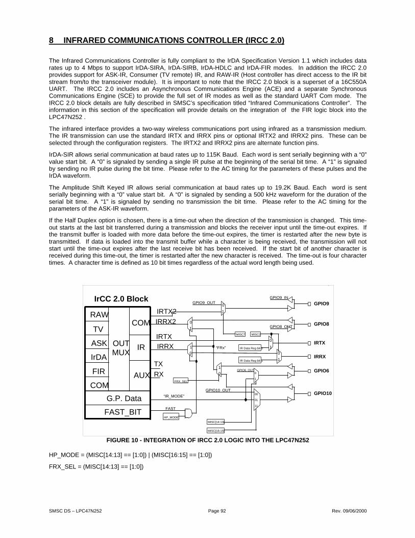
SMSC DS – LPC47N252 Page 92 Rev. 09/06/2000
8 INFRARED COMMUNICATIONS CONTROLLER (IRCC 2.0)
The Infrared Communications Controller is fully compliant to the IrDA Specification Version 1.1 which includes datarates up to 4 Mbps to support IrDA-SIRA, IrDA-SIRB, IrDA-HDLC and IrDA-FIR modes. In addition the IRCC 2.0provides support for ASK-IR, Consumer (TV remote) IR, and RAW-IR (Host controller has direct access to the IR bitstream from/to the transceiver module). It is important to note that the IRCC 2.0 block is a superset of a 16C550AUART. The IRCC 2.0 includes an Asynchronous Communications Engine (ACE) and a separate SynchronousCommunications Engine (SCE) to provide the full set of IR modes as well as the standard UART Com mode. TheIRCC 2.0 block details are fully described in SMSC’s specification titled “Infrared Communications Controller”. Theinformation in this section of the specification will provide details on the integration of the FIR logic block into theLPC47N252 .
The infrared interface provides a two-way wireless communications port using infrared as a transmission medium.The IR transmission can use the standard IRTX and IRRX pins or optional IRTX2 and IRRX2 pins. These can beselected through the configuration registers. The IRTX2 and IRRX2 pins are alternate function pins.
IrDA-SIR allows serial communication at baud rates up to 115K Baud. Each word is sent serially beginning with a “0”value start bit. A “0” is signaled by sending a single IR pulse at the beginning of the serial bit time. A “1” is signaledby sending no IR pulse during the bit time. Please refer to the AC timing for the parameters of these pulses and theIrDA waveform.
The Amplitude Shift Keyed IR allows serial communication at baud rates up to 19.2K Baud. Each word is sentserially beginning with a “0” value start bit. A “0” is signaled by sending a 500 kHz waveform for the duration of theserial bit time. A “1” is signaled by sending no transmission the bit time. Please refer to the AC timing for theparameters of the ASK-IR waveform.
If the Half Duplex option is chosen, there is a time-out when the direction of the transmission is changed. This time-out starts at the last bit transferred during a transmission and blocks the receiver input until the time-out expires. Ifthe transmit buffer is loaded with more data before the time-out expires, the timer is restarted after the new byte istransmitted. If data is loaded into the transmit buffer while a character is being received, the transmission will notstart until the time-out expires after the last receive bit has been received. If the start bit of another character isreceived during this time-out, the timer is restarted after the new character is received. The time-out is four charactertimes. A character time is defined as 10 bit times regardless of the actual word length being used.
GPIO9
GPIO8
IRTX
IRRX
GPIO6
GPIO10
GPIO6_OUT
GPIO10_OUT
GPIO8_OUT
GPIO9_OUT
IRTX2
IRRX2
IRTX
IRRX
TX
RX
GPIO9_INIrCC 2.0 Block
RAW
TV
ASK
IrDA
FIR
COM
OUTMUX
COM
IR
AUX
FAST_BIT
G.P. Data
HP_MODE
FAST
MISC7
1
MISC[14:13]
MISC[16:15]
FRX_SEL
MISC2
0
0IR Data Reg bit-0
IR Data Reg bit-1
1
1
00
01
11
0
1
1
0
0
0
1
1
0
“FRx”
“IR_MODE”
FIGURE 10 - INTEGRATION OF IRCC 2.0 LOGIC INTO THE LPC47N252
HP_MODE = (MISC[14:13] == [1:0]) | (MISC[16:15] == [1:0])
FRX_SEL = (MISC[14:13] == [1:0])

SMSC DS – LPC47N252 Page 93 Rev. 09/06/2000
8.1 IRRX/IRTX PIN ENABLE
When MISC2=0 the IRRX and IRTX pins are enabled as when IrCC 2.0 (LD5) is activated or enabled and the IRCC2.0 Output Mux is set to use the IR Port, otherwise the IRTX pin is tri-stated. When MISC2=1, the IRRX and IRTXpins are always enabled as they can be bit banged through the IR Data Register, bits 1 and 0 respectively. Seesection 25.3, Multiplexing_1 Register – MISC [7:0] on page 290.
Therefore, if the IR interface is on IRRX (pin 21) and IRTX (pin 20), then MISC2 allows the IR interface to be switchedbetween the IRCC 2.0 block and the IR Data Register. The IR Data Register is only available from the host, and islocated at index register 98. This register is available through the Mailbox Register Interface.
8.2 IR REGISTERS - LOGICAL DEVICE 5
In order to support the Infrared Communications Controller ten configuration registers are included in Logical Device5. Refer to the Configuration section of this specification for details.
Base I/O Addresses
550 UART
Table 72 - Asynchronous Communications Engine (UART) RegisterREGISTER
INDEX BASE I/O RANGEFIXED REGISTER BASE
OFFSETS
0x60, 0x61 [0x100:0x0FF8]
ON 8 BYTE BOUNDARIES
+0 : RB/TB LSB div
+1 : IER MSB div
+2 : IIR/FCR+3 : LCR+4 : MCR
+5 : LSR+6 : MSR
+7 : SCR
Register 0x60 stores the MSB and 0x61 the LSB of the 550-UART’s 16 bit Base Address.
Fast IR/SCE
Table 73 - Synchronous Communications Engine (SCE) RegistersREGISTERINDEX BASE I/O RANGE
FIXED REGISTER BASEOFFSETS
0x62, 0x63 [0x100:0x0FF8]
ON 8 BYTE BOUNDARIES
+0 : Register Block, address 0
+1 : Register Block, address 1+2 : Register Block, address 2
+3 : Register Block, address 3+4 : Register Block, address 4+5 : Register Block, address 5
+6 : Register Block, address 6+7 : SCE Master Control Register
Register 0x60 stores the MSB and 0x61 the LSB of the 550-UART’s 16 bit Base Address.
Note: Refer to the Infrared Communications Controller (IRCC 2.0) Specification for register details.
Note: If Base I/O Address is set below 0x100 then no decode will occur.
8.3 IR DMA CHANNELS
DMA channel 0, 1, 2 or 3 may be selected for use with the IRCC 2.0 logic through the configuration registers ofLogical Device 5. Refer to the Configuration section of this specification for further details on setting the DMAchannel and to the IRCC 2.0 specification for details on IR DMA transfers.

SMSC DS – LPC47N252 Page 94 Rev. 09/06/2000
8.4 IR IRQS
The interrupt for the IRCC 2.0 logic is selectable through the configuration registers for logical device 5. Refer to theConfiguration section of this specification for further details on setting the interrupt and to the IRCC 2.0 specificationfor details on IR IRQ events.
8.4.1 SOFTWARE SELECT REGISTERS A AND B
The Software Select A and Software Select B registers in the LPC47N252 configuration space in Logical DeviceNumber 5 are directly connected to the read-only IrCC 2.0 Software Select A & B registers in SCE Register BlockThree.
The LPC47N252 Software Select A register is LD5:CRF7, the LPC47N252 Software Select B register is LD5:CRF8.These registers are R/W.
Writing to LD5:CRF7 is the only way to revise the contents of the Software Select A register in the IrCC 2.0. Writingthe contents of the Software Select A register can only be done in the configuration state and only after the LDN hasbeen set to “5” and the CSR has been initialized to “F7H”. The default value of this register after power up is 00H(Table 74).
Writing to LD5:CRF8 is the only way to revise the contents of the Software Select B register in the IrCC 2.0. Writingthe contents of the Software Select B register can only be done in the configuration state and only after the LDN hasbeen set to “5” and the CSR has been initialized to “F8H”. The default value of this register after power up is 00H(Table 74).
Table 74 - LPC47N252 Software Select A&B RegistersD7 D6 D5 D4 D3 D2 D1 D0 DEFAULT
LD5:CRF7 R/W Software Select A 0x00
LD5:CRF8 R/W Software Select B 0x00
8.5 IR HALF DUPLEX TIMEOUT
LD5:CRF2 is the FDC37C97X IR Half Duplex Time-Out register (Table 75). In the LPC47N252, this register is linkedto the IrCC 2.0 IR Half Duplex Time-Out register.
In the LPC47N252, these two registers must behave like the other IrCC 2.0 legacy controls where either sourceuniformly updates the value of both registers when either register is explicitly written via the LPC interface or followinga device-level POR. IrCC 2.0 software resets do not affect these registers.
The IR Half Duplex Time-Out constrains the timing of transmit/receive direction mode changes in the IrCC 2.0. TheIR Half Duplex Time-Out is started as each IR message data bit is transferred and prevents direction mode changesuntil the time-out expires. The timer is restarted whenever new data is transferred in the current direction mode.
The IR Half Duplex Time-Out is programmable from 0 to 25.5ms in 100µs increments, as follows:
IR HALF DUPLEX TIME-OUT = (CRF2) x 100 s
Table 75 - IR Half Duplex Time-Out RegisterD7 D6 D5 D4 D3 D2 D1 D0 DEFAULT
LD5:CRF2 R/W IR HALF DUPLEX TIME-OUT 0x03
8.6 IRTX OUTPUT PINS DEFAULT
The IRCC 2.0 IRTX pins default at power-up to “output”, “low” to prevent infrared transceiver damage. This defaultbehavior applies to both the dedicated IRTX2 pin and to GPIO9 (see MISC[7, 2] bits of the Multiplexing_1 Register –MISC [7:0] on page 290.)
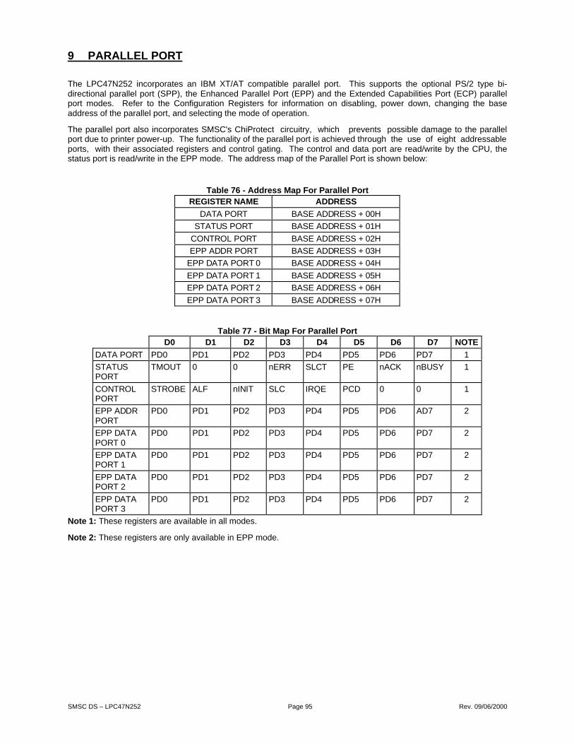
SMSC DS – LPC47N252 Page 95 Rev. 09/06/2000
9 PARALLEL PORT
The LPC47N252 incorporates an IBM XT/AT compatible parallel port. This supports the optional PS/2 type bi-directional parallel port (SPP), the Enhanced Parallel Port (EPP) and the Extended Capabilities Port (ECP) parallelport modes. Refer to the Configuration Registers for information on disabling, power down, changing the baseaddress of the parallel port, and selecting the mode of operation.
The parallel port also incorporates SMSC's ChiProtect circuitry, which prevents possible damage to the parallelport due to printer power-up. The functionality of the parallel port is achieved through the use of eight addressableports, with their associated registers and control gating. The control and data port are read/write by the CPU, thestatus port is read/write in the EPP mode. The address map of the Parallel Port is shown below:
Table 76 - Address Map For Parallel PortR EGIST ER N A ME A DD RESS
D AT A POR T BASE ADD RESS + 00H
STATU S POR T BASE ADD RESS + 01H
C ON TR OL POR T BASE ADD RESS + 02H
EPP AD DR PORT BASE ADD RESS + 03H
EPP D ATA PORT 0 BASE ADD RESS + 04H
EPP D ATA PORT 1 BASE ADD RESS + 05H
EPP D ATA PORT 2 BASE ADD RESS + 06H
EPP D ATA PORT 3 BASE ADD RESS + 07H
Table 77 - Bit Map For Parallel PortD 0 D 1 D 2 D 3 D 4 D 5 D 6 D 7 N OT E
D AT A POR T PD0 PD1 PD2 PD3 PD4 PD5 PD6 PD7 1
STATU SPOR T
T MOUT 0 0 nER R SLC T PE nAC K nBU SY 1
C ON TR OLPOR T
STR OBE ALF nIN IT SLC IRQE PCD 0 0 1
EPP AD DR POR T
PD0 PD1 PD2 PD3 PD4 PD5 PD6 AD7 2
EPP D ATAPOR T 0
PD0 PD1 PD2 PD3 PD4 PD5 PD6 PD7 2
EPP D ATAPOR T 1
PD0 PD1 PD2 PD3 PD4 PD5 PD6 PD7 2
EPP D ATAPOR T 2
PD0 PD1 PD2 PD3 PD4 PD5 PD6 PD7 2
EPP D ATAPOR T 3
PD0 PD1 PD2 PD3 PD4 PD5 PD6 PD7 2
Note 1: These registers are available in all modes.
Note 2: These registers are only available in EPP mode.

SMSC DS – LPC47N252 Page 96 Rev. 09/06/2000
Table 78 - Parallel Port Connector pin MapH OST
C ON NEC TOR PIN N U MB ER STA ND A RD EPP ECP
1 129 nStrobe nWr ite nStrobe
2-9 124-121,
119-116
PData<0:7> PData<0:7> PData<0:7>
10 115 nAck Intr nAck
11 114 Busy nWait Busy, Peri phAck( 3)
12 113 PE ( NU ) PEr ror ,nAckR everse(3)
13 112 Sel ect ( NU ) Sel ect
14 128 N al f nDatastb nALF,
H ostAck( 3)
15 127 N Er ror ( NU ) nFaul t(1)nPeri phR equest( 3)
16 126 N Init ( NU ) nInit( 1) nRever seRqst( 3)
17 125 N Selecti n nAddr str b nSelectIn( 1,3)
(1) = Compatible Mode
(3) = High Speed Mode
Note: For the cable interconnection required for ECP support and the Slave Connector pin numbers, refer to theIEEE P1284 D2.0 Standard, “Standard Signaling Method for a Bi-directional Parallel Peripheral Interface for PersonalComputers”, September 10, 1993. This document is available from the IEEE.
9.1 IBM XT/AT COMPATIBLE, BI-DIRECTIONAL AND EPP MODES
9.1.1 REGISTER DEFINITION
9.1.1.1 DATA PORT - ADDRESS OFFSET = 00H
The Data Port is located at an offset of '00H' from the base address. The data register is cleared at initialization byRESET. During a WRITE operation, the Data Register latches the contents of the internal data bus. The contents ofthis register are buffered (non inverting) and output onto the PD0 - PD7 ports. During a READ operation in SPPmode, PD0 - PD7 ports are buffered (not latched) and output to the host CPU.
9.1.1.2 STATUS PORT -ADDRESS OFFSET = 01H
The Status Port is located at an offset of '01H' from the base address. The contents of this register are latched forthe duration of a read cycle. The bits of the Status Port are defined as follows:
BIT 0 TMOUT - TIME OUTThis bit is valid in EPP mode only and indicates that a 10 µsec time out has occured on the EPP bus. A logic “0”means that no time out error has occured; a logic “1” means that a time out error has been detected. This bit iscleared by a RESET. Writing a one to this bit clears the time out status bit. On a write, this bit is self clearing anddoes not require a write of a “0”. Writing a “0” to this bit has no effect.
Note: The clearing of this bit is controlled by the Timeout_Select bit in the CnfgB Shadow register LDN 3 CRF1[7].When the Timeout_Select bit is ‘0’ (default), the Timeout bit is cleared on the trailing edge of a ‘read’ to the EPPStatus register. When the Timeout_Select bit is ‘1’, the Timeout bit is cleared on a write of ‘1’ to the Timeout bit in theEPP Status register. The Timeout bit in the EPP Status register is cleared by a Hard Reset regardless of the state ofthe Timeout_Select bit.

SMSC DS – LPC47N252 Page 97 Rev. 09/06/2000
BITS 1, 2are not implemented as register bits, during a read of the Printer Status Register these bits are a low level.
BIT 3 nERR - nERRORThe level on the nERROR input is read by the CPU as bit 3 of the Printer Status Register. A logic 0 means an errorhas been detected; a logic “1” means no error has been detected.
BIT 4 SLCT - PRINTER SELECTED STATUSThe level on the SLCT input is read by the CPU as bit 4 of the Printer Status Register. A logic “1” means the printeris on line; a logic 0 means it is not selected.
BIT 5 PE - PAPER ENDThe level on the PE input is read by the CPU as bit 5 of the Printer Status Register. A logic “1” indicates a paper end;a logic 0 indicates the presence of paper.
BIT 6 nACK - nACKNOWLEDGEThe level on the nACK input is read by the CPU as bit 6 of the Printer Status Register. A logic “0” means that theprinter has received a character and can now accept another. A logic “1” means that it is still processing the lastcharacter or has not received the data.
BIT 7 nBUSY - nBUSYThe complement of the level on the BUSY input is read by the CPU as bit 7 of the Printer Status Register. A logic “0”in this bit means that the printer is busy and cannot accept a new character. A logic “1” means that it is ready toaccept the next character.
9.1.1.3 CONTROL PORT – ADDRESS OFFSET = 02H
The Control Port is located at an offset of '02H' from the base address. The Control Register is initialized by theRESET input, bits 0 to 5 only being affected; bits 6 and 7 are hard wired low.
BIT 0 STROBE - STROBEThis bit is inverted and output onto the nSTROBE output.
BIT 1 ALF - AUTOFEEDThis bit is inverted and output onto the nALF output. A logic “1” causes the printer to generate a line feed after eachline is printed. A logic “0” means no autofeed.
BIT 2 nINIT - nINITIATE OUTPUTThis bit is output onto the nINIT output without inversion.
BIT 3 SLCTIN - PRINTER SELECT INPUTThis bit is inverted and output onto the nSLCTIN output. A logic “1” on this bit selects the printer; a logic “0” meansthe printer is not selected.
BIT 4 IRQE - INTERRUPT REQUEST ENABLEThe interrupt request enable bit when set to a high level may be used to enable interrupt requests from the ParallelPort to the CPU. An interrupt request is generated on the IRQ port by a positive going nACK input. When the IRQEbit is programmed low the IRQ is disabled.
BIT 5 PCD - PARALLEL CONTROL DIRECTIONParallel Control Direction is not valid in printer mode. In printer mode, the direction is always out regardless of thestate of this bit. In bi-directional, EPP or ECP mode, a logic 0 means that the printer port is in output mode (write); alogic “1” means that the printer port is in input mode (read).
BITS 6 and 7 – ReservedRead only logic zero.

SMSC DS – LPC47N252 Page 98 Rev. 09/06/2000
9.1.1.4 EPP ADDRESS PORT - ADDRESS OFFSET = 03H
The EPP Address Port is located at an offset of '03H' from the base address. The address register is cleared atinitialization by RESET. During a WRITE operation, the contents of the internal data bus DB0-DB7 are buffered (noninverting) and output onto the PD0 - PD7 ports. An LPC I/O write cycle causes an EPP ADDRESS WRITE cycle to beperformed, during which the data is latched for the duration of the EPP write cycle. During a READ operation, PD0 -PD7 ports are read. An LPC I/O read cycle causes an EPP ADDRESS READ cycle to be performed and the dataoutput to the host CPU, the deassertion of ADDRSTB latches the PData for the duration of the read cycle. Thisregister is only available in EPP mode.
9.1.1.5 EPP DATA PORT 0 -ADDRESS OFFSET = 04H
The EPP Data Port 0 is located at an offset of '04H' from the base address. The data register is cleared atinitialization by RESET. During a WRITE operation, the contents of the internal data bus DB0-DB7 are buffered (noninverting) and output onto the PD0 - PD7 ports. An LPC I/O write cycle causes an EPP DATA WRITE cycle to beperformed, during which the data is latched for the duration of the EPP write cycle. During a READ operation, PD0 -PD7 ports are read. An LPC I/O read cycle causes an EPP READ cycle to be performed and the data output to thehost CPU, the deassertion of DATASTB latches the PData for the duration of the read cycle. This register is onlyavailable in EPP mode.
9.1.1.6 EPP DATA PORT 1 - ADDRESS OFFSET = 05H
The EPP Data Port 1 is located at an offset of '05H' from the base address. Refer to EPP DATA PORT 0 for adescription of operation. This register is only available in EPP mode.
9.1.1.7 EPP DATA PORT 2 -ADDRESS OFFSET = 06H
The EPP Data Port 2 is located at an offset of '06H' from the base address. Refer to EPP DATA PORT 0 for adescription of operation. This register is only available in EPP mode.
9.1.1.8 EPP DATA PORT 3 - ADDRESS OFFSET = 07H
The EPP Data Port 3 is located at an offset of '07H' from the base address. Refer to EPP DATA PORT 0 for adescription of operation. This register is only available in EPP mode.
9.1.1.9 EPP 1.9 OPERATION
When the EPP mode is selected in the configuration register, the standard and bi-directional modes are alsoavailable. If no EPP Read, Write or Address cycle is currently executing, then the PDx bus is in the standard or bi-directional mode, and all output signals (STROBE, ALF, INIT) are as set by the SPP Control Port and direction iscontrolled by PCD of the Control port.
In EPP mode, the system timing is closely coupled to the EPP timing. For this reason, a watchdog timer is requiredto prevent system lockup. The timer indicates if more than 10µsec have elapsed from the start of the EPP cycle tonWAIT being deasserted (after command). If a time-out occurs, the current EPP cycle is aborted and the time-outcondition is indicated in Status bit 0.
During an EPP cycle, if STROBE is active, it overrides the EPP write signal forcing the PDx bus to always be in awrite mode and the nWRITE signal to always be asserted.
9.1.1.9.1 Software Constraints
Before an EPP cycle is executed, the software must ensure that the control register bit PCD is a logic "0" (i.e. a 04Hor 05H should be written to the Control port). If the user leaves PCD as a logic "1", and attempts to perform an EPPwrite, the chip is unable to perform the write (because PCD is a logic "1") and will appear to perform an EPP read onthe parallel bus, no error is indicated.

SMSC DS – LPC47N252 Page 99 Rev. 09/06/2000
9.1.1.9.2 EPP 1.9 Write
The timing for a write operation (address or data) is shown in timing diagram EPP Write Data or Address cycle. Thechip inserts wait states into the LPC I/O write cycle until it has been determined that the write cycle can complete.The write cycle can complete under the following circumstances:
If the EPP bus is not ready (nWAIT is active low) when nDATASTB or nADDRSTB goes active then the write cancomplete when nWAIT goes inactive high.
If the EPP bus is ready (nWAIT is inactive high) then the chip must wait for it to go active low before changing thestate of nDATASTB, nWRITE or nADDRSTB. The write can complete once nWAIT is determined inactive.
9.1.1.9.2.1 Write Sequence of Operation
The host initiates an I/O write cycle to the selected EPP register.
If WAIT is not asserted, the chip must wait until WAIT is asserted.
The chip places address or data on PData bus, clears PDIR, and asserts nWRITE.
Chip asserts nDATASTB or nADDRSTRB indicating that PData bus contains valid information, and the WRITE signalis valid.
Peripheral deasserts nWAIT, indicating that any setup requirements have been satisfied and the chip may begin thetermination phase of the cycle.
The chip deasserts nDATASTB or nADDRSTRB, this marks the beginning of the termination phase. If it has notalready done so, the peripheral should latch the information byte now.
The chip latches the data from the internal data bus for the PData bus and drives the sync that indicates that no morewait states are required followed by the TAR to complete the write cycle.
Peripheral asserts nWAIT, indicating to the host that any hold time requirements have been satisfied andacknowledging the termination of the cycle.
Chip may modify nWRITE and nPDATA in preparation for the next cycle.
9.1.1.9.3 EPP 1.9 Read
The timing for a read operation (data) is shown in timing diagram EPP Read Data cycle. The chip inserts wait statesinto the LPC I/O read cycle until it has been determined that the read cycle can complete. The read cycle cancomplete under the following circumstances:
If the EPP bus is not ready (nWAIT is active low) when nDATASTB goes active then the read can complete whennWAIT goes inactive high.
If the EPP bus is ready (nWAIT is inactive high) then the chip must wait for it to go active low before changing thestate of WRITE or before nDATASTB goes active. The read can complete once nWAIT is determined inactive.
9.1.1.9.3.1 Read Sequence of Operation
The host initiates an I/O read cycle to the selected EPP register.
If WAIT is not asserted, the chip must wait until WAIT is asserted.
The chip tri-states the PData bus and deasserts nWRITE.
Chip asserts nDATASTB or nADDRSTRB indicating that PData bus is tri-stated, PDIR is set and the nWRITE signalis valid.
Peripheral drives PData bus valid.
Peripheral deasserts nWAIT, indicating that PData is valid and the chip may begin the termination phase of the cycle.
The chip latches the data from the PData bus for the internal data bus and deasserts nDATASTB or nADDRSTRB.This marks the beginning of the termination phase.
The chip drives the sync that indicates that no more wait states are required and drives the valid data onto theLAD[3:0] signals, followed by the TAR to complete the read cycle.

SMSC DS – LPC47N252 Page 100 Rev. 09/06/2000
Peripheral tri-states the PData bus and asserts nWAIT, indicating to the host that the PData bus is tri-stated.
Chip may modify nWRITE, PDIR and nPDATA in preparation for the next cycle.
9.1.1.10 EPP 1.7 OPERATION
When the EPP 1.7 mode is selected in the configuration register, the standard and bi-directional modes are alsoavailable. If no EPP Read, Write or Address cycle is currently executing, then the PDx bus is in the standard or bi-directional mode, and all output signals (STROBE, AUTOFD, INIT) are as set by the SPP Control Port and directionis controlled by PCD of the Control port.
In EPP mode, the system timing is closely coupled to the EPP timing. For this reason, a watchdog timer is requiredto prevent system lockup. The timer indicates if more than 10usec have elapsed from the start of the EPP cycle tothe end of the cycle. If a time-out occurs, the current EPP cycle is aborted and the time-out condition is indicated inStatus bit 0.
9.1.1.10.1 Software Constraints
Before an EPP cycle is executed, the software must ensure that the control register bits D0, D1 and D3 are set tozero. Also, bit D5 (PCD) is a logic "0" for an EPP write or a logic "1" for and EPP read.
9.1.1.10.1.1 EPP 1.7 Write
The timing for a write operation (address or data) is shown in timing diagram EPP 1.7 Write Data or Address cycle.The chip inserts wait states into the I/O write cycle when nWAIT is active low during the EPP cycle. This can be usedto extend the cycle time. The write cycle can complete when nWAIT is inactive high.
9.1.1.10.1.1.1 Write Sequence of Operation
The host sets PDIR bit in the control register to a logic "0". This asserts nWRITE.
The host initiates an I/O write cycle to the selected EPP register.
The chip places address or data on PData bus.
Chip asserts nDATASTB or nADDRSTRB indicating that PData bus contains valid information, and the WRITE signalis valid.
If nWAIT is asserted, the chip inserts wait states into I/O write cycle until the peripheral deasserts nWAIT or a time-out occurs.
The chip drives the final sync, deasserts nDATASTB or nADDRSTRB and latches the data from the internal data busfor the PData bus.
Chip may modify nWRITE, PDIR and nPDATA in preparation of the next cycle.
9.1.1.10.1.2 EPP 1.7 Read
The timing for a read operation (data) is shown in timing diagram EPP 1.7 Read Data cycle. The chip inserts waitstates into the I/O read cycle when nWAIT is active low during the EPP cycle. This can be used to extend the cycletime. The read cycle can complete when nWAIT is inactive high.
Read Sequence of Operation:
The host sets PDIR bit in the control register to a logic "1". This deasserts nWRITE and tri-states the PData bus.
The host initiates an I/O read cycle to the selected EPP register.
Chip asserts nDATASTB or nADDRSTRB indicating that PData bus is tri-stated, PDIR is set and the nWRITE signalis valid.
If nWAIT is asserted, the chip inserts wait states into the I/O read cycle until the peripheral deasserts nWAIT or atime-out occurs.
The Peripheral drives PData bus valid.
The Peripheral deasserts nWAIT, indicating that PData is valid and the chip may begin the termination phase of thecycle.

SMSC DS – LPC47N252 Page 101 Rev. 09/06/2000
The chip drives the final sync and deasserts nDATASTB or nADDRSTRB.
Peripheral tri-states the PData bus.
Chip may modify nWRITE, PDIR and nPDATA in preparation of the next cycle.
Table 79 - EPP Pin DescriptionsEPP
SIGNAL EPP NAME TYPE EPP DESCRIPTION
NWRITE nWrite O This signal is active low. It denotes a write operation.
PD<0:7> Address/Data I/O Bi-directional EPP byte wide address and data bus.
INTR Interrupt I This signal is active high and positive edge triggered. (Passthrough with no inversion, Same as SPP).
WAIT nWait I This signal is active low. It is driven inactive as a positiveacknowledgement from the device that the transfer of data iscompleted. It is driven active as an indication that the deviceis ready for the next transfer.
DATASTB nData Strobe O This signal is active low. It is used to denote data read orwrite operation.
RESET nReset O This signal is active low. When driven active, the EPP deviceis reset to its initial operational mode.
ADDRSTB nAddressStrobe
O This signal is active low. It is used to denote address read orwrite operation.
PE Paper End I Same as SPP mode.
SLCT PrinterSelected Status
I Same as SPP mode.
NERR Error I Same as SPP mode.
PDIR Parallel PortDirection
O This output shows the direction of the data transfer on theparallel port bus. A low means an output/write condition and ahigh means an input/read condition. This signal is normally alow (output/write) unless PCD of the control register is set or ifan EPP read cycle is in progress.
Note 1: SPP and EPP can use 1 common register.
Note 2: nWrite is the only EPP output that can be over-ridden by SPP control port during an EPP cycle. For correctEPP read cycles, PCD is required to be a low.
SMSC DS – LPC47N252 Page 102 Rev. 09/06/2000
9.2 EXTENDED CAPABILITIES PARALLEL PORT
ECP provides a number of advantages, some of which are listed below. The individual features are explained ingreater detail in the remainder of this section.
High performance half-duplex forward and reverse channel
Interlocked handshake, for fast reliable transfer
Optional single byte RLE compression for improved throughput (64:1)
Channel addressing for low-cost peripherals
Maintains link and data layer separation
Permits the use of active output drivers
Permits the use of adaptive signal timing
Peer-to-peer capability
9.2.1 VOCABULARY
The following terms are used in this document:
assert: When a signal asserts it transitions to a "true" state, when a signal deasserts it transitions to a "false" state.
forward: Host to Peripheral communication.
reverse: Peripheral to Host communication.
PWord: A port word; equal in size to the width of the ISA interface. For this implementation, PWord is always 8 bits.
1: A high level.
0: A low level.
These terms may be considered synonymous:
PeriphClk, nAck
HostAck, nALF
PeriphAck, Busy
nPeriphRequest, nFault
nReverseRequest, nInit
nAckReverse, PError
Xflag, Select
ECPMode, nSelectln
HostClk, nStrobe
Note: Refer to IEEE 1284 Extended Capabilities Port Protocol and ISA Interface Standard, Rev 1.14, July 14, 1993.This document is available from Microsoft.

SMSC DS – LPC47N252 Page 103 Rev. 09/06/2000
The bit map of the Extended Parallel Port registers is described in Table 80.
Table 80 - Bit Map Of The Extended Parallel Port RegistersD7 D6 D5 D4 D3 D2 D1 D0 NOTE
data PD7 PD6 PD5 PD4 PD3 PD2 PD1 PD0
ecpAFifo Addr/RLE Address or RLE field 2
dsr nBusy nAck PError Select nFault 0 0 0 1
dcr 0 0 Direction ackIntEn SelectIn nInit alf strobe 1
cFifo Parallel Port Data FIFO 002
ecpDFifo ECP Data FIFO 2
tFifo Test FIFO 2
cnfgA 0 0 0 1 0 0 0 0
cnfgB compress intrValue 0 0 0 0 0 0
ecr MODE nErrIntrEn dmaEn serviceIntr full empty
Note 1: These registers are available in all modes.Note 2: All FIFOs use one common 16 byte FIFO.
9.2.2 ECP IMPLEMENTATION STANDARD
This specification describes the standard ISA interface to the Extended Capabilities Port (ECP). All LPC devicessupporting ECP must meet the requirements contained in this section or the port will not be supported by Microsoft.For a description of the ECP Protocol, please refer to the IEEE 1284 Extended Capabilities Port Protocol and ISAInterface Standard, Rev. 1.14, July 14, 1993. This document is available from Microsoft.
9.2.3 DESCRIPTION
The port is software and hardware compatible with existing parallel ports so that it may be used as a standard LPTport if ECP is not required. The port is designed to be simple and requires a small number of gates to implement. Itdoes not do any "protocol" negotiation, rather it provides an automatic high burst-bandwidth channel that supportsDMA for ECP in both the forward and reverse directions.
Small FIFOs are employed in both forward and reverse directions to smooth data flow and improve the maximumbandwidth requirement. The size of the FIFO is 16 bytes deep. The port supports an automatic handshake for thestandard parallel port to improve compatibility mode transfer speed.
The port also supports run length encoded (RLE) decompression (required) in hardware. Compression isaccomplished by counting identical bytes and transmitting an RLE byte that indicates how many times the next byte isto be repeated. Decompression simply intercepts the RLE byte and repeats the following byte the specified number oftimes. Hardware support for compression is optional.
Table 81 - ECP Pin DescriptionsNAME TYPE DESCRIPTION
nStrobe O During write operations nStrobe registers data or address into the slave onthe asserting edge (handshakes with Busy).
PData 7:0 I/O Contains address or data or RLE data.
nAck I Indicates valid data driven by the peripheral when asserted. This signalhandshakes with nALF in reverse.
PeriphAck (Busy) I This signal deasserts to indicate that the peripheral can accept data. Thissignal handshakes with nStrobe in the forward direction. In the reversedirection this signal indicates whether the data lines contain ECP commandinformation or data. The peripheral uses this signal to flow control in theforward direction. It is an "interlocked" handshake with nStrobe. PeriphAckalso provides command information in the reverse direction.

SMSC DS – LPC47N252 Page 104 Rev. 09/06/2000
NAME TYPE DESCRIPTION
PError
(nAckReverse)
I Used to acknowledge a change in the direction the transfer (asserted =forward). The peripheral drives this signal low to acknowledgenReverseRequest. It is an "interlocked" handshake with nReverseRequest.The host relies upon nAckReverse to determine when it is permitted to drivethe data bus.
Select I Indicates printer on line.
nALF(HostAck)
O Requests a byte of data from the peripheral when asserted, handshaking withnAck in the reverse direction. In the forward direction this signal indicateswhether the data lines contain ECP address or data. The host drives thissignal to flow control in the reverse direction. It is an "interlocked" handshakewith nAck. HostAck also provides command information in the forward phase.
nFault(nPeriphRequest)
I Generates an error interrupt when asserted. This signal provides amechanism for peer-to-peer communication. This signal is valid only in theforward direction. During ECP Mode the peripheral is permitted (but notrequired) to drive this pin low to request a reverse transfer. The request ismerely a "hint" to the host; the host has ultimate control over the transferdirection. This signal would be typically used to generate an interrupt to thehost CPU.
nInit O Sets the transfer direction (asserted = reverse, deasserted = forward). Thispin is driven low to place the channel in the reverse direction. The peripheralis only allowed to drive the bi-directional data bus while in ECP Mode andHostAck is low and nSelectIn is high.
nSelectIn O Always deasserted in ECP mode.
9.2.4 REGISTER DEFINITIONS
The register definitions are based on the standard IBM addresses for LPT. All of the standard printer ports aresupported. The additional registers attach to an upper bit decode of the standard LPT port definition to avoidconflict with standard ISA devices. The port is equivalent to a generic parallel port interface and may be operated inthat mode. The port registers vary depending on the mode field in the ecr. The table below lists these dependencies.Operation of the devices in modes other that those specified is undefined.
Table 82 - ECP Register DefinitionsNAME ADDRESS (Note 1) ECP MODES FUNCTION
data +000h R/W 000-001 Data Register
ecpAFifo +000h R/W 011 ECP FIFO (Address)
dsr +001h R/W All Status Register
dcr +002h R/W All Control Register
cFifo +400h R/W 010 Parallel Port Data FIFO
ecpDFifo +400h R/W 011 ECP FIFO (DATA)
tFifo +400h R/W 110 Test FIFO
cnfgA +400h R 111 Configuration Register A
cnfgB +401h R/W 111 Configuration Register B
ecr +402h R/W All Extended Control Register
Note 1: These addresses are added to the parallel port base address as selected by configuration register

SMSC DS – LPC47N252 Page 105 Rev. 09/06/2000
Table 83 - Extended Control Register ModeMODE DESCRIPTION*
000 SPP mode
001 PS/2 Parallel Port mde
010 Parallel Port Data FIFO mode
011 ECP Parallel Port mode
100 EPP mode (If this option is enabled in the configuration registers)
101 (Reserved)
110 Test mode
111 Configuration mode*Refer to ECR Register Description on page 107
9.2.4.1 DATA and ecpAFifo PORT -ADDRESS OFFSET = 00H
9.2.4.1.1 Modes 000 and 001 (Data Port)
The Data Port is located at an offset of '00H' from the base address. The data register is cleared at initialization byRESET. During a WRITE operation, the Data Register latches the contents of the data bus. The contents of thisregister are buffered (non inverting) and output onto the PD0 - PD7 ports. During a oREAD operation, PD0 - PD7ports are read and output to the host CPU.
9.2.4.1.2 Mode 011 (ECP FIFO - Address/RLE)
A data byte written to this address is placed in the FIFO and tagged as an ECP Address/RLE. The hardware at theECP port transmitts this byte to the peripheral automatically. The operation of this register is ony defined for theforward direction (direction is 0). Refer to the FIGURE 89 - EC P PAR A LL EL PORT FORW A RD T IMING on page321.
9.2.4.2 DEVICE STATUS REGISTER (dsr) - ADDRESS OFFSET = 01H
The Status Port is located at an offset of '01H' from the base address. Bits 0-2 are not implemented as register bits,during a read of the Printer Status Register these bits are a low level. The bits of the Status Port are defined asfollows:
BIT 3 nFaultThe level on the nFault input is read by the CPU as bit 3 of the Device Status Register.
BIT 4 SelectThe level on the Select input is read by the CPU as bit 4 of the Device Status Register.
BIT 5 PErrorThe level on the PError input is read by the CPU as bit 5 of the Device Status Register. Printer Status Register.
BIT 6 nAckThe level on the nAck input is read by the CPU as bit 6 of the Device Status Register.
BIT 7 nBusyThe complement of the level on the BUSY input is read by the CPU as bit 7 of the Device Status Register.
9.2.4.3 DEVICE CONTROL REGISTER (dcr) - ADDRESS OFFSET = 02H
The Control Register is located at an offset of '02H' from the base address. The Control Register is initialized to zeroby the RESET input, bits 0 to 5 only being affected; bits 6 and 7 are hard wired low.
BIT 0 STROBE - STROBEThis bit is inverted and output onto the nSTROBE output.
SMSC DS – LPC47N252 Page 106 Rev. 09/06/2000
BIT 1 ALF - AUTOFEEDThis bit is inverted and output onto the nALF output. A logic “1” causes the printer to generate a line feed after eachline is printed. A logic “0” means no autofeed.
BIT 2 nINIT - nINITIATE OUTPUTThis bit is output onto the nINIT output without inversion.
BIT 3 SELECTINThis bit is inverted and output onto the nSLCTIN output. A logic “1” on this bit selects the printer; a logic “0” meansthe printer is not selected.
BIT 4 ackIntEn - INTERRUPT REQUEST ENABLEThe interrupt request enable bit when set to a high level may be used to enable interrupt requests from theParallel Port to the CPU due to a low to high transition on the nACK input. Refer to the description of the interruptunder Operation, Interrupts.
BIT 5 DIRECTIONIf mode=000 or mode=010, this bit has no effect and the direction is always out regardless of the state of this bit. Inall other modes, Direction is valid and a logic 0 means that the printer port is in output mode (write); a logic “1” meansthat the printer port is in input mode (read).
BITS 6 and 7 -ReservedThese bits are read only logic zero.
9.2.4.4 cFifo (Parallel Port Data FIFO) - ADDRESS OFFSET = 400h
Mode = 010Bytes written or DMAed from the system to this FIFO are transmitted by a hardware handshake to the peripheralusing the standard parallel port protocol. Transfers to the FIFO are byte aligned. This mode is only defined for theforward direction.
9.2.4.5 ecpDFifo (ECP Data FIFO) -ADDRESS OFFSET = 400H
Mode = 011Bytes written or DMAed from the system to this FIFO, when the direction bit is “0”, are transmitted by a hardwarehandshake to the peripheral using the ECP parallel port protocol. Transfers to the FIFO are byte aligned.
Data bytes from the peripheral are read under automatic hardware handshake from ECP into this FIFO when thedirection bit is “1”. Reads or DMAs from the FIFO will return bytes of ECP data to the system.
9.2.4.6 tFifo (Test FIFO Mode) - ADDRESS OFFSET = 400H
Mode = 110Data bytes may be read, written or DMAed to or from the system to this FIFO in any direction. Data in the tFIFO willnot be transmitted to the to the parallel port lines using a hardware protocol handshake. However, data in the tFIFOmay be displayed on the parallel port data lines.
The tFIFO will not stall when overwritten or underrun. If an attempt is made to write data to a full tFIFO, the new datais not accepted into the tFIFO. If an attempt is made to read data from an empty tFIFO, the last data byte is re-readagain. The full and empty bits must always keep track of the correct FIFO state. The tFIFO will transfer data at themaximum ISA rate so that software may generate performance metrics. The FIFO size and interrupt threshold canbe determined by writing bytes to the FIFO and checking the full and serviceIntr bits.
The writeIntrThreshold can be derermined by starting with a full tFIFO, setting the direction bit to “0” and emptying it abyte at a time until serviceIntr is set. This may generate a spurious interrupt, but will indicate that the threshold hasbeen reached.
The readIntrThreshold can be derermined by setting the direction bit to “1” and filling the empty tFIFO a byte at a timeuntil serviceIntr is set. This may generate a spurious interrupt, but will indicate that the threshold has been reached.
Data bytes are always read from the head of tFIFO regardless of the value of the direction bit. For example if 44h,33h, 22h is written to the FIFO, then reading the tFIFO will return 44h, 33h, 22h in the same order as was written.

SMSC DS – LPC47N252 Page 107 Rev. 09/06/2000
9.2.4.7 ister A) - ADDRESS OFFSET = 400H
Mode = 111This register is a read only register. When read, 10H is returned. This indicates to the system that this is an 8-bitimplementation. (PWord = 1 byte)
9.2.4.8 cnfgB (Configuration Register B) - ADDRESS OFFSET = 401H
Mode = 111
BIT 7 compressThis bit is read only. During a read it is a low level. This means that this chip does not support hardware RLEcompression. It does support hardware de-compression!
BIT 6 intrValueReturns the value on the ISA iRq line to determine possible conflicts.
BITS 5:0 ReservedDuring a read are a low level. These bits cannot be written.
9.2.4.9 ecr (Extended Control Register) - ADDRESS OFFSET = 402H
Mode = allThis register controls the extended ECP parallel port functions.
BITS 7 - 5These bits are Read/Write and select the Mode.
BIT 4 nErrIntrEnRead/Write (Valid only in ECP Mode)
1: Disables the interrupt generated on the asserting edge of nFault.
0: Enables an interrupt pulse on the high to low edge of nFault. Note that an interrupt will be generated if nFault isasserted (interrupting) and this bit is written from a 1 to a 0. This prevents interrupts from being lost in the timebetween the read of the ecr and the write of the ecr.
BIT 3 dmaEnRead/Write
1: Enables DMA (DMA starts when serviceIntr is 0).
0: Disables DMA unconditionally.
BIT 2 serviceIntrRead/Write
1: Disables DMA and all of the service interrupts.
0: Enables one of the following 3 cases of interrupts. Once one of the 3 service interrupts has occurred serviceIntr bitshall be set to a 1 by hardware. It must be reset to 0 to re-enable the interrupts. Writing this bit to a 1 will not causean interrupt.
case dmaEn=1:
During DMA (this bit is set to a “1” when terminal count is reached).
case dmaEn=0 direction=0:
This bit shall be set to 1 whenever there are writeIntrThreshold or more bytes free in the FIFO.
case dmaEn=0 direction=1:
This bit shall be set to 1 whenever there are readIntrThreshold or more valid bytes to be read from the FIFO.

SMSC DS – LPC47N252 Page 108 Rev. 09/06/2000
BIT 1 fullRead only
1: The FIFO cannot accept another byte or the FIFO is completely full.
0: The FIFO has at least 1 free byte.
BIT 0 emptyRead only
1: The FIFO is completely empty.
0: The FIFO contains at least 1 byte of data.
Table 84 - Extended Control RegisterR/W MODE
000: Standard Parallel Port Mode . In this mode the FIFO is reset and common collector drivers are used on thecontrol lines (nStrobe, nALF, nInit and nSelectIn). Setting the direction bit will not tri-state the output driversin this mode.
001: PS/2 Parallel Port Mode. Same as above except that direction may be used to tri-state the data lines andreading the data register returns the value on the data lines and not the value in the data register. All drivershave active pull-ups (push-pull).
010: Parallel Port FIFO Mode. This is the same as 000 except that bytes are written or DMAed to the FIFO. FIFOdata is automatically transmitted using the standard parallel port protocol. Note that this mode is only usefulwhen direction is 0. All drivers have active pull-ups (push-pull).
011: ECP Parallel Port Mode. In the forward direction (direction is 0) bytes placed into the ecpDFifo and byteswritten to the ecpAFifo are placed in a single FIFO and transmitted automatically to the peripheral using ECPProtocol. In the reverse direction (direction is 1) bytes are moved from the ECP parallel port and packed intobytes in the ecpDFifo. All drivers have active pull-ups (push-pull).
100: Selects EPP Mode: In this mode, EPP is selected if the EPP supported option is selected in configurationregister L3-CRF0. All drivers have active pull-ups (push-pull).
101: Reserved
110: Test Mode. In this mode the FIFO may be written and read, but the data will not be transmitted on theparallel port. All drivers have active pull-ups (push-pull).
111: Configuration Mode. In this mode the confgA, confgB registers are accessible at 0x400 and 0x401. Alldrivers have active pull-ups (push-pull).
9.2.5 OPERATION
9.2.5.1 Mode Switching/Software Control
Software will execute P1284 negotiation and all operation prior to a data transfer phase under programmed I/Ocontrol (mode 000 or 001). Hardware provides an automatic control line handshake, moving data between the FIFOand the ECP port only in the data transfer phase (modes 011 or 010).
Setting the mode to 011 or 010 will cause the hardware to initiate data transfer.
If the port is in mode 000 or 001 it may switch to any other mode. If the port is not in mode 000 or 001 it can only beswitched into mode 000 or 001. The direction can only be changed in mode 001.
Once in an extended forward mode the software should wait for the FIFO to be empty before switching back tomode 000 or 001. In this case all control signals will be deasserted before the mode switch. In an ecp reverse modethe software waits for all the data to be read from the FIFO before changing back to mode 000 or 001. Since theautomatic hardware ecp reverse handshake only cares about the state of the FIFO it may have acquired extra datawhich will be discarded. It may in fact be in the middle of a transfer when the mode is changed back to 000 or 001. Inthis case the port will deassert nALF independent of the state of the transfer. The design shall not cause glitches onthe handshake signals if the software meets the constraints above.

SMSC DS – LPC47N252 Page 109 Rev. 09/06/2000
9.2.5.2 ECP Operation
Prior to ECP operation the Host must negotiate on the parallel port to determine if the peripheral supports the ECPprotocol. This is a somewhat complex negotiation carried out under program control in mode 000.
After negotiation, it is necessary to initialize some of the port bits. The following are required:
Set Direction = 0, enabling the drivers.
Set strobe = 0, causing the nStrobe signal to default to the deasserted state.
Set alf = 0, causing the nALF signal to default to the deasserted state.
Set mode = 011 (ECP Mode)
ECP address/RLE bytes or data bytes may be sent automatically by writing the ecpAFifo or ecpDFifo respectively.
Note that all FIFO data transfers are byte wide and byte aligned. Address/RLE transfers are byte-wide and onlyallowed in the forward direction.
The host may switch directions by first switching to mode = 001, negotiating for the forward or reverse channel,setting direction to “1” or “0”, then setting mode = 011. When direction is 1 the hardware shall handshake for eachECP read data byte and attempt to fill the FIFO. Bytes may then be read from the ecpDFifo as long as it is notempty.
ECP transfers may also be accomplished (albeit slowly) by handshaking individual bytes under program control inmode = 001, or 000.
9.2.5.2.1 Termination from ECP Mode
Termination from ECP Mode is similar to the termination from Nibble/Byte Modes. The host is permitted to terminatefrom ECP Mode only in specific well-defined states. The termination can only be executed while the bus is in theforward direction. To terminate while the channel is in the reverse direction, it must first be transitioned into theforward direction.
9.2.5.2.2 Command/Data
ECP Mode supports two advanced features to improve the effectiveness of the protocol for some applications. Thefeatures are implemented by allowing the transfer of normal 8 bit data or 8 bit commands.
When in the forward direction, normal data is transferred when HostAck is high and an 8 bit command is transferredwhen HostAck is low. The most significant bit of the command indicates whether it is a run-length count (forcompression) or a channel address.
When in the reverse direction, normal data is transferred when PeriphAck is high and an 8 bit command is transferredwhen PeriphAck is low. The most significant bit of the command is always “0”. Reverse channel addresses areseldom used and may not be supported in hardware
Table 85 - Forward Channel Commands (HostAck Low) & Reverse Channel Commands (PeripAck Low)
D7 D[6:0]
0 Run-Length Count (0-127)(mode 0011 0X00 only)
1 Channel Address (0-127)
9.2.5.2.3 Data Compression
The ECP port supports run length encoded (RLE) decompression in hardware and can transfer compressed data to aperipheral. Run length encoded (RLE) compression in hardware is not supported. To transfer compressed data inECP mode, the compression count is written to the ecpAFifo and the data byte is written to the ecpDFifo.
Compression is accomplished by counting identical bytes and transmitting an RLE byte that indicates how manytimes the next byte is to be repeated. Decompression simply intercepts the RLE byte and repeats the following bytethe specified number of times. When a run-length count is received from a peripheral, the subsequent data byte isreplicated the specified number of times. A run-length count of zero specifies that only one byte of data isrepresented by the next data byte, whereas a run-length count of 127 indicates that the next byte should beexpanded to 128 bytes. To prevent data expansion, however, run-length counts of zero should be avoided.

SMSC DS – LPC47N252 Page 110 Rev. 09/06/2000
9.2.5.2.4 Pin Definition
The drivers for nStrobe, nALF, nInit and nSelectIn are open-collector in mode 000 and are push-pull in all othermodes.
9.2.5.2.4.1 LPC Connections
The interface can never stall causing the host to hang. The width of data transfers is strictly controlled on an I/Oaddress basis per this specification. All FIFO-DMA transfers are byte wide, byte aligned and end on a byte boundary.(The PWord value can be obtained by reading Configuration Register A, cnfgA, described in the next section.)Single byte wide transfers are always possible with standard or PS/2 mode using program control of the controlsignals.
9.2.5.2.4.2 Interrupts
The interrupts are enabled by serviceIntr in the ecr register.
serviceIntr = 1 Disables the DMA and all of the service interrupts.
serviceIntr = 0 Enables the selected interrupt condition. If the interrupting condition is valid, then the interrupt isgenerated immediately when this bit is changed from a 1 to a 0. This can occur during Programmed I/O if the numberof bytes removed or added from/to the FIFO does not cross the threshold.
The interrupt generated is ISA friendly in that it must pulse the interrupt line low, allowing for interrupt sharing. Aftera brief pulse low following the interrupt event, the interrupt line is tri-stated so that other interrupts may assert.
An interrupt is generated when:
For DMA transfers: When serviceIntr is “0”, dmaEn is 1 and the DMA TC is received.
For Programmed I/O:
When serviceIntr is 0, dmaEn is 0, direction is “0” and there are writeIntrThreshold or more free bytes in the FIFO.Also, an interrupt is generated when serviceIntr is cleared to 0 whenever there are writeIntrThreshold or more freebytes in the FIFO.
When serviceIntr is “0”, dmaEn is 0, direction is “1” and there are readIntrThreshold or more bytes in the FIFO. (2)An interrupt is also generated when serviceIntr is cleared to “0” whenever there are readIntrThreshold or more bytesin the FIFO.
When nErrIntrEn is 0 and nFault transitions from high to low or when nErrIntrEn is set from “1” to “0” and nFault isasserted.
When ackIntEn is “1” and the nAck signal transitions from a low to a high.
9.2.5.2.4.3 FIFO Operation
The FIFO threshold is set in the chip configuration registers. All data transfers to or from the parallel port canproceed in DMA or Programmed I/O (non-DMA) mode as indicated by the selected mode. The FIFO is used byselecting the Parallel Port FIFO mode or ECP Parallel Port Mode. (FIFO test mode will be addressed separately.)After a reset, the FIFO is disabled. Each data byte is transferred by a Programmed I/O cycle or PDRQ depending onthe selection of DMA or Programmed I/O mode.
The following paragraphs detail the operation of the FIFO flow control. In these descriptions, <threshold> rangesfrom 1 to 16. The parameter FIFOTHR, which the user programs, is one less and ranges from 0 to 15.
A low threshold value (i.e. 2) results in longer periods of time between service requests, but requires faster servicingof the request for both read and write cases. The host must be very responsive to the service request. This is thedesired case for use with a "fast" system.
A high value of threshold (i.e. 12) is used with a "sluggish" system by affording a long latency period after a servicerequest, but results in more frequent service requests.
9.2.5.2.4.4 DMA Transfers
DMA transfers are always to or from the ecpDFifo, tFifo or CFifo. DMA utilizes the standard PC DMA services. Touse the DMA transfers, the host first sets up the direction and state as in the programmed I/O case. Then it programsthe DMA controller in the host with the desired count and memory address. Lastly it sets dmaEn to 1 and serviceIntr

SMSC DS – LPC47N252 Page 111 Rev. 09/06/2000
to 0. The ECP requests DMA transfers from the host by encoding the LDRQ# pin. The DMA will empty or fill theFIFO using the appropriate direction and mode. When the terminal count in the DMA controller is reached, aninterrupt is generated and serviceIntr is asserted, disabling DMA. In order to prevent possible blocking of refreshrequests a DMA cycle shall not be requested for more than 32 DMA cycles in a row. The FIFO is enabled directly bythe host initiating a DMA cycle for the requested channel, and addresses need not be valid. An interrupt is generatedwhen a TC cycle is received. (Note: The only way to properly terminate DMA transfers is with a TC cycle.)
DMA may be disabled in the middle of a transfer by first disabling the host DMA controller. Then setting serviceIntr to1, followed by setting dmaEn to 0, and waiting for the FIFO to become empty or full. Restarting the DMA isaccomplished by enabling DMA in the host, setting dmaEn to 1, followed by setting serviceIntr to 0.
9.2.5.2.4.5 DMA Mode - Transfers from the FIFO to the Host
Note: In the reverse mode, the peripheral may not continue to fill the FIFO if it runs out of data to transfer, even if thechip continues to request more data from the peripheral.
The ECP requests a DMA cycle whenever there is data in the FIFO. The DMA controller must respond to the requestby reading data from the FIFO. The ECP stops requesting DMA cycles when the FIFO becomes empty or when a TCcycle is received, indicating that no more data is required. If the ECP stops requesting DMA cycles due to the FIFOgoing empty, then a DMA cycle is requested again as soon as there is one byte in the FIFO. If the ECP stopsrequesting DMA cycles due to the TC cycle, then a DMA cycle is requested again when there is one byte in the FIFO,and serviceIntr has been re-enabled.
9.2.5.2.4.6 Programmed I/O Mode or Non-DMA Mode
The ECP or parallel port FIFOs may also be operated using interrupt driven programmed I/O. Software candetermine the writeIntrThreshold, readIntrThreshold, and FIFO depth by accessing the FIFO in Test Mode.Programmed I/O transfers are to the ecpDFifo at 400H and ecpAFifo at 000H or from the ecpDFifo located at 400H,or to/from the tFifo at 400H. To use the programmed I/O transfers, the host first sets up the direction and state, setsdmaEn to 0 and serviceIntr to 0. The ECP requests programmed I/O transfers from the host by activating the PINTRpin. The programmed I/O will empty or fill the FIFO using the appropriate direction and mode.
Note: A threshold of 16 is equivalent to a threshold of 15. These two cases are treated the same.
9.2.5.2.4.7 Programmed I/O - Transfers from the FIFO to the Host
In the reverse direction an interrupt occurs when serviceIntr is 0 and readIntrThreshold bytes are available in theFIFO. If at this time the FIFO is full it can be emptied completely in a single burst, otherwise readIntrThresholdbytes may be read from the FIFO in a single burst.
readIntrThreshold = (16-<threshold>) data bytes in FIFO
An interrupt is generated when serviceIntr is 0 and the number of bytes in the FIFO is greater than or equal to (16-<threshold>). (If the threshold = 12, then the interrupt is set whenever there are 4-16 bytes in the FIFO). The hostmust respond to the request by reading data from the FIFO. This process is repeated until the last byte is transferredout of the FIFO. If at this time the FIFO is full, it can be completely emptied in a single burst, otherwise a minimum of(16-<threshold>) bytes may be read from the FIFO in a single burst.
9.2.5.2.4.8 Programmed I/O - Transfers from the Host to the FIFO
In the forward direction an interrupt occurs when serviceIntr is 0 and there are writeIntrThreshold or more bytes freein the FIFO. At this time if the FIFO is empty it can be filled with a single burst before the empty bit needs to bere-read. Otherwise it may be filled with writeIntrThreshold bytes.
writeIntrThreshold = (16-<threshold>) free bytes in FIFO
An interrupt is generated when serviceIntr is 0 and the number of bytes in the FIFO is less than or equal to<threshold>. (If the threshold = 12, then the interrupt is set whenever there are 12 or less bytes of data in the FIFO.)The host must respond to the request by writing data to the FIFO. If at this time the FIFO is empty, it can becompletely filled in a single burst, otherwise a minimum of (16-<threshold>) bytes may be written to the FIFO in asingle burst. This process is repeated until the last byte is transferred into the FIFO.
9.3 THE PARALLEL PORT PHYSICAL INTERFACE (PPPI)
The Parallel Port Physical Interface (PPPI) has three source modes of operation. The PPPI Mode determines thesource device that controls the PPPI.
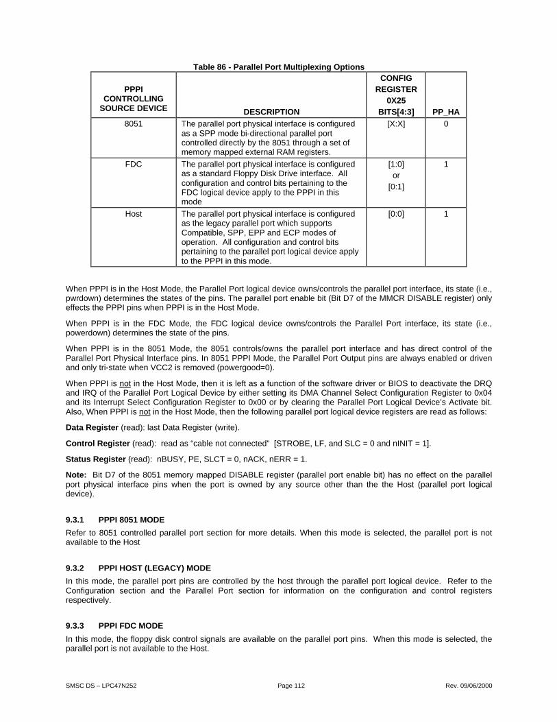
SMSC DS – LPC47N252 Page 112 Rev. 09/06/2000
Table 86 - Parallel Port Multiplexing Options
PPPICONTROLLING
SOURCE DEVICE DESCRIPTION
CONFIGREGISTER
0X25
BITS[4:3] PP_HA
8051 The parallel port physical interface is configuredas a SPP mode bi-directional parallel portcontrolled directly by the 8051 through a set ofmemory mapped external RAM registers.
[X:X] 0
FDC The parallel port physical interface is configuredas a standard Floppy Disk Drive interface. Allconfiguration and control bits pertaining to theFDC logical device apply to the PPPI in thismode
[1:0]or
[0:1]
1
Host The parallel port physical interface is configuredas the legacy parallel port which supportsCompatible, SPP, EPP and ECP modes ofoperation. All configuration and control bitspertaining to the parallel port logical device applyto the PPPI in this mode.
[0:0] 1
When PPPI is in the Host Mode, the Parallel Port logical device owns/controls the parallel port interface, its state (i.e.,pwrdown) determines the states of the pins. The parallel port enable bit (Bit D7 of the MMCR DISABLE register) onlyeffects the PPPI pins when PPPI is in the Host Mode.
When PPPI is in the FDC Mode, the FDC logical device owns/controls the Parallel Port interface, its state (i.e.,powerdown) determines the state of the pins.
When PPPI is in the 8051 Mode, the 8051 controls/owns the parallel port interface and has direct control of theParallel Port Physical Interface pins. In 8051 PPPI Mode, the Parallel Port Output pins are always enabled or drivenand only tri-state when VCC2 is removed (powergood=0).
When PPPI is not in the Host Mode, then it is left as a function of the software driver or BIOS to deactivate the DRQand IRQ of the Parallel Port Logical Device by either setting its DMA Channel Select Configuration Register to 0x04and its Interrupt Select Configuration Register to 0x00 or by clearing the Parallel Port Logical Device’s Activate bit.Also, When PPPI is not in the Host Mode, then the following parallel port logical device registers are read as follows:
Data Register (read): last Data Register (write).
Control Register (read): read as “cable not connected” [STROBE, LF, and SLC = 0 and nINIT = 1].
Status Register (read): nBUSY, PE, SLCT = 0, nACK, nERR = 1.
Note: Bit D7 of the 8051 memory mapped DISABLE register (parallel port enable bit) has no effect on the parallelport physical interface pins when the port is owned by any source other than the the Host (parallel port logicaldevice).
9.3.1 PPPI 8051 MODE
Refer to 8051 controlled parallel port section for more details. When this mode is selected, the parallel port is notavailable to the Host
9.3.2 PPPI HOST (LEGACY) MODE
In this mode, the parallel port pins are controlled by the host through the parallel port logical device. Refer to theConfiguration section and the Parallel Port section for information on the configuration and control registersrespectively.
9.3.3 PPPI FDC MODE
In this mode, the floppy disk control signals are available on the parallel port pins. When this mode is selected, theparallel port is not available to the Host.
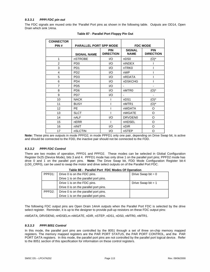
SMSC DS – LPC47N252 Page 113 Rev. 09/06/2000
9.3.3.1 PPPI FDC pin out
The FDC signals are muxed onto the ‘Parallel Port pins as shown in the following table. Outputs are OD14, OpenDrain which sink 14ma.
Table 87 - Parallel Port Floppy Pin Out
CONNECTORPIN # PARALLEL PORT SPP MODE FDC MODE
SIGNAL NAMEPIN
DIRECTIONSIGNALNAME
PINDIRECTION
1 nSTROBE I/O nDS0 (O)*
2 PD0 I/O nINDEX I
3 PD1 I/O nTRK0 I
4 PD2 I/O nWP I
5 PD3 I/O nRDATA I
6 PD4 I/O nDSKCHG I
7 PD5 I/O - -
8 PD6 I/O nMTR0 (O)*
9 PD7 I/O - -
10 NACK I nDS1 (O)*
11 BUSY I nMTR1 (O)*
12 PE I nWDATA O
13 SLCT I nWGATE O
14 nALF I/O DRVDEN0 O
15 nERR I nHDSEL O
16 nINIT I/O nDIR O
17 nSLCTIN I/O nSTEP O
Note: These pins are outputs in mode PPFD2; in mode PPFD1 only one pair, depending on Drive Swap bit, is activeand should be connected to the FDD, the inactive pair should not be connected to the FDD.
9.3.3.2 PPPI FDC Control
There are two modes of operation, PPFD1 and PPFD2. These modes can be selected in Global ConfigurationRegister 0x25 (Device Mode), bits 3 and 4. PPFD1 mode has only drive 1 on the parallel port pins; PPFD2 mode hasdrive 0 and 1 on the parallel port pins. Note: The Drive Swap bit, FDD Mode Configuration Register bit-4(LD0_CRF0), can be used to swap the motor and drive select outputs on of the Parallel Port FDC.
Table 88 - Parallel Port FDC Modes Of OperationPPFD1: Drive 0 is on the FDC pins.
Drive 1 is on the parallel port pins.
Drive Swap bit = 0
Drive 1 is on the FDC pins.Drive 0 is on the parallel port pins.
Drive Swap bit = 1
PPFD2: Drive 0 is on the parallel port pins.Drive 1 is on the parallel port pins.
The following FDC output pins are Open Drain 14mA outputs when the Parallel Port FDC is selected by the driveselect register. Reminder, it is up to the designer to provide pull-up resistors on these FDC output pins:
nWDATA, DRVDEN0, nHDSELm nWGATE, nDIR, nSTEP, nDS1, nDS0, nMTR0, nMTR1.
9.3.3.3 PPPI 8051 Control
In this mode, the parallel port pins are controlled by the 8051 through a set of three on-chip memory mappedregisters. The memory mapped registers are the PAR PORT STATUS, the PAR PORT CONTROL, and the PARPORT DATA registers. In this mode, the parallel port pins are not controlled by the parallel port logical device. Referto the 8051 section of this specification for information on these control registers.
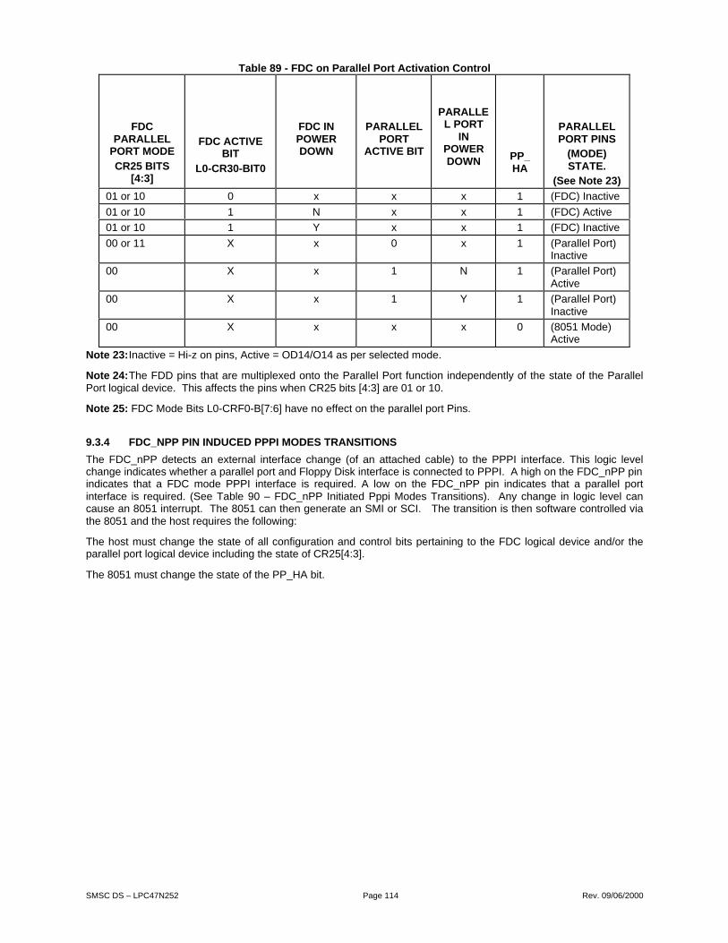
SMSC DS – LPC47N252 Page 114 Rev. 09/06/2000
Table 89 - FDC on Parallel Port Activation Control
FDCPARALLEL
PORT MODE
CR25 BITS[4:3]
FDC ACTIVEBIT
L0-CR30-BIT0
FDC INPOWERDOWN
PARALLELPORT
ACTIVE BIT
PARALLEL PORT
INPOWERDOWN PP_
HA
PARALLELPORT PINS
(MODE)STATE.
(See Note 23)
01 or 10 0 x x x 1 (FDC) Inactive
01 or 10 1 N x x 1 (FDC) Active
01 or 10 1 Y x x 1 (FDC) Inactive
00 or 11 X x 0 x 1 (Parallel Port)Inactive
00 X x 1 N 1 (Parallel Port)Active
00 X x 1 Y 1 (Parallel Port)Inactive
00 X x x x 0 (8051 Mode)Active
Note 23:Inactive = Hi-z on pins, Active = OD14/O14 as per selected mode.
Note 24:The FDD pins that are multiplexed onto the Parallel Port function independently of the state of the ParallelPort logical device. This affects the pins when CR25 bits [4:3] are 01 or 10.
Note 25: FDC Mode Bits L0-CRF0-B[7:6] have no effect on the parallel port Pins.
9.3.4 FDC_NPP PIN INDUCED PPPI MODES TRANSITIONS
The FDC_nPP detects an external interface change (of an attached cable) to the PPPI interface. This logic levelchange indicates whether a parallel port and Floppy Disk interface is connected to PPPI. A high on the FDC_nPP pinindicates that a FDC mode PPPI interface is required. A low on the FDC_nPP pin indicates that a parallel portinterface is required. (See Table 90 – FDC_nPP Initiated Pppi Modes Transitions). Any change in logic level cancause an 8051 interrupt. The 8051 can then generate an SMI or SCI. The transition is then software controlled viathe 8051 and the host requires the following:
The host must change the state of all configuration and control bits pertaining to the FDC logical device and/or theparallel port logical device including the state of CR25[4:3].
The 8051 must change the state of the PP_HA bit.

SMSC DS – LPC47N252 Page 115 Rev. 09/06/2000
Table 90 – FDC_nPP Initiated Pppi Modes Transitions
PREVIOUS STATE
NEXTSTATE
PPPI MODE
(SOURCEDEVICE
CONTROLLINGTHE PPPI)
TRANSITION DESCRIPTION
CONFIG
REGISTER0X25
BITS[4:3]
PP_HA
0=8051
CONTROL
FDC_nPPpin
0=FDCINTERFACE
REQUEST
8051 —›FDC The PPPI transitions from being configured asan 8051-controlled SPP mode bi-directionalparallel to being configured as a standardFloppy Disk Drive interface. As part of thisPPPI mode transition, the host must changethe state of all configuration and control bitspertaining to the FDC logical device includingthe state of CR25[4:3].
[X:X] 0 0
Host —›FDC The PPPI transitions from being configured asa legacy parallel port that supports Compatible,SPP, EPP and ECP modes of operation tobeing configured as a standard Floppy DiskDrive interface. As part of this PPPI modetransition, the host must change the state of allconfiguration and control bits pertaining to theFDC logical device including the state ofCR25[4:3].
[0:0] 1 0
FDC—›8051 The PPPI transitions from being configured asa standard Floppy Disk Drive interface to abeing configured as a SPP mode bi-directionalparallel port controlled directly by the 8051through a set of memory mapped externalRAM registers. All configuration and controlbits pertaining to the FDC logical device do notapply to the PPPI in this mode. As part of thistransition, the 8051 must change the state ofthe PP_HA bit from one to zero.
[1:0]or
[0:1]
1 1
FDC—› Host The PPPI transitions from being configured asa standard Floppy Disk Drive interface to beingconfigured as a legacy parallel port thatsupports Compatible, SPP, EPP and ECPmodes of operation. As part of this transition,the host must change the state of allconfiguration and control bits pertaining to theparallel port logical device including the stateof CR25[4:3].
[1:0]or
[0:1]
1 0

SMSC DS – LPC47N252 Page 116 Rev. 09/06/2000
10 AUTO POWER MANAGEMENT
Auto Power Management (APM) capabilities are provided for the following logical devices: Floppy Disk, UART,Infrared and the Parallel Port. For each logical device, two types of power management are provided; directpowerdown and auto powerdown.
10.1 SYSTEM POWER MANAGEMENT
See the “8051 System Power Management” section for details.
FDC Power ManagementDirect power management is controlled through Global Configuration Register 22 (CR22). Refer to CR22 in theConfiguration section for more information. Auto Power Management is enabled through bit-0 of CR23. When set,this bit allows the FDC to enter powerdown when all of the following conditions have been met:
The motor enable pins of the FDC’s DOR register are inactive (zero). The LPC47N252 must be idle; the MSRregister = 80h and the FDC’s INTerrupt = 0 (INT may be high even if MSR = 80H due to polling interrupts). The headunload timer must have expired. The Auto powerdown timer (10msec) must have timed out. An internal timer isinitiated as soon as the auto powerdown command is enabled. The LPC47N252 is then powered down when all theconditions are met. Disabling the auto powerdown mode cancels the timer and holds the FDC block out of autopowerdown.
Note: At least 8us delay should be added when exiting FDC Auto Powerdown mode. If the operating environment issuch that this delay cannot be guaranteed, the auto powerdown mode should not be used and Direct powerdownmode should be used instead. The Direct powerdown mode requires at least 8us delay at 250K bits/secconfiguration and 4us delay at 500K bits/sec. The delay should be added so that the internal microcontroller canprepare itself to accept commands.
10.2 DSR FROM POWERDOWN
Bit 6 of the FDC’s DSR register is another FDC powerdown bit. If DSR powerdown is used when the LPC47N252 isin auto powerdown, the DSR powerdown will override the auto powerdown. However, when the LPC47N252 isawakened from DSR powerdown, the auto powerdown will once again become effective.
10.3 WAKE UP FROM AUTO POWERDOWN
If the LPC47N252 enters the Powerdown State through the auto powerdown mode, then the LPC47N252 can beawakened by reset or by appropriate access to certain registers.
If a hardware or software reset is used then the LPC47N252 will go through the normal reset sequence. If the accessis through the selected registers, then the FDC resumes operation as though it was never in powerdown. Besidesactivating the nRESET_OUT pin or one of the software reset bits in the DOR or DSR registers, the following registeraccesses will wake up the LPC47N252:
Setting any one of the motor enable bits in the DOR register (reading the DOR does not awaken the LPC47N252).
A read from the MSR register.
A read from or a write to the Data register.
Once awake, the FDC will reinitiate the auto powerdown timer for 10 ms. The LPC47N252 will powerdown againwhen all the powerdown conditions are satisfied.
10.4 REGISTER BEHAVIOR
Table 91 shows the AT and PS/2 (including Model 30) configuration registers available. It also shows the type ofaccess permitted. In order to maintain software transparency, access to all the registers is maintained. As Table 91shows, two sets of registers are distinguished based on whether their access results in the LPC47N252 remaining inpowerdown state or exiting it.
Access to all other registers is possible without awakening the LPC47N252. These registers can be accessed duringpowerdown without changing the status of the LPC47N252. A read from these registers will reflect the true status asshown in the register description in the FDC section. Writes to these registers will result in the LPC47N252 retainingthe data and subsequently reflecting it when the LPC47N252 awakens.
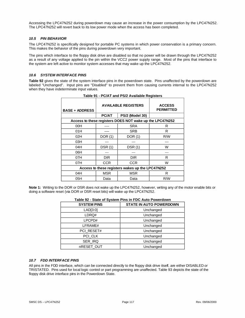
SMSC DS – LPC47N252 Page 117 Rev. 09/06/2000
Accessing the LPC47N252 during powerdown may cause an increase in the power consumption by the LPC47N252.The LPC47N252 will revert back to its low power mode when the access has been completed.
10.5 PIN BEHAVIOR
The LPC47N252 is specifically designed for portable PC systems in which power conservation is a primary concern.This makes the behavior of the pins during powerdown very important.
The pins which interface to the floppy disk drive are disabled so that no power will be drawn through the LPC47N252as a result of any voltage applied to the pin within the VCC2 power supply range. Most of the pins that interface tothe system are left active to monitor system accesses that may wake up the LPC47N252.
10.6 SYSTEM INTERFACE PINS
Table 92 gives the state of the system interface pins in the powerdown state. Pins unaffected by the powerdown arelabeled "Unchanged". Input pins are "Disabled" to prevent them from causing currents internal to the LPC47N252when they have indeterminate input values.
Table 91 - PC/AT and PS/2 Available Registers
B ASE + A DD R ESS
A VA IL A BL E R EGIST ER S A CC ESSPER MIT TED
PC/AT PS/2 ( Mo del 30)
A ccess t o t hese registers DOES NOT wake u p th e L PC 47N 252
00H - -- - SRA R
01H - -- - SRB R
02H D OR ( 1) D OR ( 1) R /W
03H - -- - -- - --
04H D SR ( 1) D SR ( 1) W
06H - -- - -- - --
07H D IR D IR R
07H C CR C CR W
A ccess t o t hese registers wakes u p t he L PC47N 252
04H M SR M SR R
05H D ata D ata R /W
N ot e 1: W ri ting to the D OR or D SR does not w ake up the LPC47N 252, how ever, w r iting any of the motor enable bi ts or doi ng a softw ar e r eset (vi a DOR or D SR r eset bits) wi ll wake up the LPC 47N252.
Table 92 - State of System Pins in FDC Auto PowerdownSYSTEM PIN S STA TE IN A U TO POWERD OWN
LAD [3:0] U nchanged
LDR Q# U nchanged
LPC PD # U nchanged
LFR AM E# U nchanged
PCI_R ESET# U nchanged
PCI_C LK U nchanged
SER _IR Q U nchanged
nRESET _OUT U nchanged
10.7 FDD INTERFACE PINS
All pi ns i n the FD D i nter face, which can be connected di rectl y to the floppy disk dri ve itsel f, ar e either D ISABLED or T RIST ATED. Pins used for local l ogi c contr ol or part pr ogram mi ng ar e unaffected. Table 93 depi cts the state of thefloppy disk dri ve inter face pi ns in the Pow er dow n State.
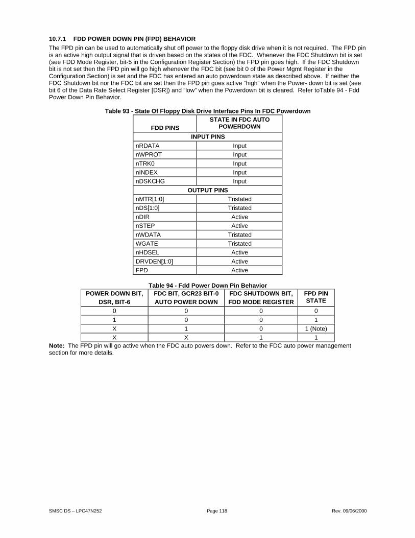
SMSC DS – LPC47N252 Page 118 Rev. 09/06/2000
10.7.1 FDD POWER DOWN PIN (FPD) BEHAVIOR
The FPD pin can be used to automatically shut off power to the floppy disk drive when it is not required. The FPD pinis an active high output signal that is driven based on the states of the FDC. Whenever the FDC Shutdown bit is set(see FDD Mode Register, bit-5 in the Configuration Register Section) the FPD pin goes high. If the FDC Shutdownbit is not set then the FPD pin will go high whenever the FDC bit (see bit 0 of the Power Mgmt Register in theConfiguration Section) is set and the FDC has entered an auto powerdown state as described above. If neither theFDC Shutdown bit nor the FDC bit are set then the FPD pin goes active “high” when the Power- down bit is set (seebit 6 of the Data Rate Select Register [DSR]) and “low” when the Powerdown bit is cleared. Refer toTable 94 - FddPower Down Pin Behavior.
Table 93 - State Of Floppy Disk Drive Interface Pins In FDC Powerdown
F DD PINSSTA TE IN F D C AU T O
POW ER D OW N
INPUT PINS
nRD AT A Input
nWPROT Input
nTR K0 Input
nIN DEX Input
nDSKC H G Input
OUT PU T PIN S
nMT R[1:0] T ri stated
nDS[1:0] T ri stated
nDIR Active
nST EP Active
nWD AT A T ri stated
W GATE T ri stated
nHD SEL Active
D RVDEN [1:0] Active
F PD Active
Table 94 - Fdd Power Down Pin BehaviorPOWER DOWN BIT,
DSR, BIT-6
FDC BIT, GCR23 BIT-0
AUTO POWER DOWN
FDC SHUTDOWN BIT,
FDD MODE REGISTER
FPD PINSTATE
0 0 0 0
1 0 0 1
X 1 0 1 (Note)
X X 1 1Note: The FPD pin will go active when the FDC auto powers down. Refer to the FDC auto power managementsection for more details.

SMSC DS – LPC47N252 Page 119 Rev. 09/06/2000
10.8 UART POWER MANAGEMENT
Direct power management is controlled by CR22. Refer to CR22 in the Configuration Section for more information.
Auto power management is enabled by CR23 bit 4 and bit 5. When set, these bits allow the following auto powermanagement operations:
The transmitter enters auto powerdown when the transmit buffer and shift register are empty.
The receiver enters powerdown when the following conditions are all met:
Receive FIFO is empty
The receiver is waiting for a start bit
Note: While in powerdown the Ring Indicator interrupt is still valid.
10.9 EXIT AUTO POWERDOWN
The transmitter exits powerdown on a write to the transmit buffer. The receiver exits auto powerdown when RXDchanges state.
10.10 PARALLEL PORT POWER MANAGEMENT
D ir ect pow er managem ent i s controll ed by CR 22. Refer to C R22 i n the C onfigurati on Secti on for m or e i nfor m ation.
Auto pow er managem ent i s enabl ed by CR 23 bi t 3. W hen set, this bi t al l ow s the EC P or EPP l ogical par al lel por t blocksto be pl aced into pow er dow n when not bei ng used.
T he EPP logic i s i n pow er dow n under any of the fol l ow ing conditions:
1) EPP i s not enabl ed i n the confi guration r egister s.2) EPP i s not selected thr ough ecr w hi l e in EC P m ode.
T he EC P logic i s i n pow er dow n under any of the fol l ow ing conditions:
1) ECP i s not enabl ed i n the confi guration r egister s.2) SPP, PS/2 Par al l el port or EPP mode is selected thr ough ecr w hi le in EC P mode.
10.11 EXIT AUTO POWERDOWN
T he parall el por t logic can change pow er dow n m odes when the ECP m ode i s changed thr ough the ecr regi ster or whenthe parall el por t mode is changed through the confi guration r egister s.

SMSC DS – LPC47N252 Page 120 Rev. 09/06/2000
11 8051 EMBEDDED CONTROLLER
11.1 8051 FUNCTIONAL OVERVIEW
The High-Performance 8051 embedded controller is a fully static CMOS core compatible with the industry- standard80C51 microcontroller. The high-performance 8051 features include:
§ 2.5X average instruction execution speed improvement over the entire instruction set; i.e., typical 4-clockinstruction cycle in high-performance 8051 vs. 12-clock instruction cycle in standard 8051.
§ Faster clock speed: 32MHz or higher vs. 16MHz in standard 8051.
§ Dual Data Pointers§ More Interrupts: Power-Fail, External Interrupt 2, External Interrupt 3, etc.
§ A set of External Memory/Mapped Control Registers provides the 80C51 core with the ability to directly controlmany functional blocks of the LPC47N252.
11.1.1 FEATURES
§ Internal 64K Flash ROM§ Programmed From Direct Parallel Interface, 8051, or LPC Host
§ 2k-Byte Lockable Boot Block§ 256 Byte Internal Scratch ROM§ 256 Bytes Internal Data RAM
§ 256 Bytes of External Data RAM§ 256 Byte External Memory/Mapped Control Register Area
§ 128 Byte Special Function Register Area§ Access to 256 Byte RTC CMOS RAM§ 8042 style Keyboard Controller Host Interface
§ Eleven Interrupt Sources§ Watch Dog Timer (WDT)
§ Ring Oscillator with Fail Safe Control
11.2 HIGH-PERFORMANCE 8051 IMPLEMENTED FEATURES
There are five significant features implemented in the high-performance 8051 core. These features, summarized inTable 95, are described more fully in the sub-sections that follow.
Table 95 - High-Performance 8051 Implemented FeaturesFEATURE VALUE DESCRIPTION
Internal RAM Size 256
(bytes)
The internal RAM size is 256 bytes to maintaincompatibility with existing implementations.
Internal Timers2 3 There are three internal Timers (T0, T1 & T2).The external inputs for Timer/Counter T0, T1, andT2, as well as the Timer/Counter 2 capture/reloadtrigger T2EX are not supported in the LPC47N252.
Serial Ports 1 There is one Serial Port.
Interrupts 11 The high-performance 8051 interrupt unit provides11 interrupt sources (see
Table 108 on page 137).

SMSC DS – LPC47N252 Page 121 Rev. 09/06/2000
11.2.1 FUNCTIONAL BLOCKS
Below are the functional blocks that the 8051 core has control of through its on-chip memory/mapped externalregisters.
§ 8042 Sytle Keyboard Controller Interface§ Extended Interrupts
§ Power Management Functions§ Direct Keyboard Scan Matrix (up to 128 keys)
§ Four channel PS/2 Interface§ Dual Access Bus Interface§ LED controls
§ RTC CMOS RAM Access§ 8051 Control of the Parallel Port Interface
§ 83 General Purpose I/O (GPIO) pins§ ACPI Embedded Controller§ PM1 Block
§ Three Pulse Width Modulators§ Dual Fan Tachometer interface
11.2.2 HIGH-PERFORMANCE 8051 CYCLE TIMING AND INSTRUCTION SET
The high-performance 8051 processor offers increased performance by executing instructions in a 4-clock cycle, asopposed to the standard 8051. The shortened bus timing improves the instruction execution rate for mostinstructions by a factor of three over the standard 8051 architectutres.
Some instructions require a different number of instruction cycles on the high-performance 8051than they do on thestandard 8051. In the standard 8051, all instructions except for MUL and DIV take one or two instruction cycles tocomplete. In the high-performance 8051 architecture, instructions can take between one and five instructions tocomplete. The average speed improvement for the entire instruction set is approximately 2.5X. See Table 328 - 8051Instruction Set on page 15 for number of cycles on individaul instruction requries.
11.3 POWERING UP OR RESETTING THE 8051
11.3.1 DEFAULT RESET CONDITIONS
The LPC47N252 has two sources of reset: a VCC1 Power On Reset (VCC1 POR) or a VCC2 POR. An LPC47N252reset from any of these sources will cause the hardware response shown in Table 101, 8051 On-Chip ExternalMemory Mapped Registers. Note that the values shown are those prior to any resident firmware control. Refer toTable 101 for the effect of each type of reset on each of the on-chip registers.
11.3.1.1 Power-Up Sequence
When the 8051 first powers up by VCC1, the ring oscillator is started, once this has stabilized, the 8051 startsexecuting from program address 00. Once running, the 8051 can access all of the registers that are on VCC1 and ifVCC2 is at 3.3V it can access all of the registers on VCC2. For on-chip registers powered by VCC1 which are resetupon VCC2 Power On Reset (VCC2 POR), it is important that 8051 firmware not initialize or write to any of theseregisters until 1ms following VCC2 = 3.3V AND PWRGD = 1 (See Table 101)
Note: In order to guarantee that the external Flash device has powered up and is ready to operate before the 8051attempts to access it, the internal VCC1 POR pulse has been extended to 20ms. The internal VCC1 POR signal isasserted upon VCC1 reaching a valid level and will remain asserted for a period of 20ms following the assertion ofthe VCC1_PWRGD pin.
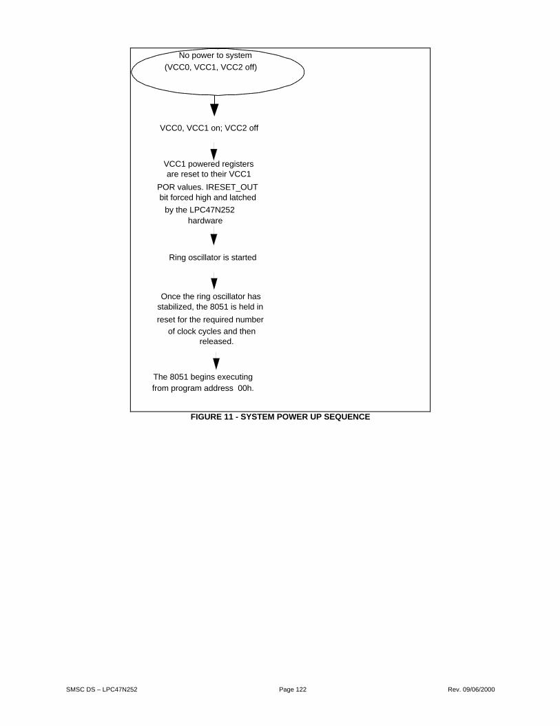
SMSC DS – LPC47N252 Page 122 Rev. 09/06/2000
No power to system
(VCC0, VCC1, VCC2 off)
Ring oscillator is started
Once the ring oscillator hasstabilized, the 8051 is held in
reset for the required number
of clock cycles and thenreleased.
VCC0, VCC1 on; VCC2 off
The 8051 begins executingfrom program address 00h.
VCC1 powered registersare reset to their VCC1
POR values. IRESET_OUTbit forced high and latched
by the LPC47N252 hardware
FIGURE 11 - SYSTEM POWER UP SEQUENCE

SMSC DS – LPC47N252 Page 123 Rev. 09/06/2000
System Reset Sequence
Note 2: In order toleasve idel mode the8051 must receive aninterrupt; typically asoftware timer interruptwill be used
System is running(Vcc2 and Vcc1 are on)
8051 is executingKeyboard firmware
Reset Event is conveyedto the8051via a
command from host orGPIO
iRESET_OUT registerbit is reset causing
nRESET_OUT pin to beasserted (See Note 1)
8051 goes into Idle Mode
StopClock
Counter= 0
StopClock
Counter= 0
No
nRESET_OUTdeasserted
Note 1:Clearing the iRESET_OUT bit caues the following:Ù 8051STP_CLK[0]=1Ù Stop Clock Counter starts decrementing
nRESET_OUT deasertedand 8051STP_CLK[0]=1
stops the 8051 clock.
Host may program theFlash memory via the
LPCBUS Flash ProgramAccess Mode
Host resets the8051STP_CLK[0] bit
8051 IRQ
8051 IRQ
No
8051 wakes up from idlemode and starts
executing from where itleft off.-
Yes
Yes
FIGURE 12 - TYPICAL SYSTEM RESET SEQUENCE
11.4 CPU RESET SEQUENCE
Often the Host CPU (x486 or Pentium) is reset by the hardware signal, CPU_RESET, which is issued by software toswitch the Processor from Protected, or “Virtual 86”, mode back to Real mode. CPU_RESET can be generated fromthe LPC47N252 8051 core or it may be generated from other logic on the PC motherboard. CPU_RESET is meantonly to reset the CPU; the rest of the system continues to run normally, including the keyboard BIOS in the 8051.
11.5 8051 CLOCK CONTROLS
The LPC47N252 has two clock source:
The 8051 may program it self to run off of an internal ring oscillator having a frequency range between 4 and 12MHz.This is not a precise clock, but is meant to provide the 8051 with a clock source when VCC2 is shut down in thesystem.
The external clock source is from a 14.318MHz TTL compatible clock. VCC2 must be powered in order for this tooccur.
11.5.1 FREQUENCY CONTROLS
The KBDCLK ENABLE bit controls the running of the 8051 PLL clock and the KBDCLK[1:0] control bits in theKSTP_CLK register (MMCR 0x7F27) select the 8051 system clock frequencies The Kahuna 8051 can run up to32MHz.
Table 96 - STOP_COUNT RegisterHOST ADDRESS 8051 ADDRESS POWER PLANE DEFAULT
- 0x7F2F VCC1 0x00
D7 D6 D5 D4 D3 D2 D1 D0
HOST TYPE - - - - - - - -
8051 TYPE R R R R R/W R/W R/W R/W
BIT NAME Reserved STP_CNT[3:0]

SMSC DS – LPC47N252 Page 124 Rev. 09/06/2000
STP_CNT[x]This defines the number of machine cycles from when the internal IRESET_OUT bit is cleared until the externalnRESET_OUT pin goes inactive high (deasserts).
Table 97 - KSTP_CLK RegisterHOST ADDRESS 8051 ADDRESS POWER PLANE DEFAULT
- 0x7F27 VCC1 0x10
D7 D6 D5 D4 D3 D2 D1 D0
HOST TYPE - - - - - - - -
8051 TYPE R/W R/W R/W R/W R R R/W R/W
BIT NAME KBDCLK[1:0]
(See Table 98)
KBCLK/
ROSC ROSCEN Reserved PLL_STOP
KBDCLKENABLE
Note 26 – When VCC1 is active and the ROSCEN bit changes from “0” to “1”, there is a delay of 6 µs max. before thering oscillator starts.
KBDCLK/ENABLEWhen the KBDCLK ENABLE bit is “0”, the 8051 PLL clock is stopped, like when the KBDCLK[1:0] = 0,0 in theFDC37C95X. When KBDCLK ENABLE is “1”, the 8051 PLL clock is running (See Table 98 - KBDCLK Control BitEncoding.)
PLL_STOPThe PLL_STOP bit D1 is used to control the power state of the 14.318MHz PLL. When the PLL_STOP bit is “1” thePLL and all of the internal clocks except for the RTC and Ring Oscillator are stopped. When the PLL_STOP bit is “0”the PLL and all of the internal clocks are running. When VCC2 is active and the PLL_STOP bit changes from “1” to“0”, there is a delay of 100µs max. before the PLL clocks are stable.
ROSCENThis bit reflects the state of the ring oscillator clock at all times. The 8051 can write this bit to start or stop the ringoscillator. Other hardware events can also start or stop this clock.
= 1 turn on ring oscillator
= 0 turn off ring oscillator
This bit is reset when the 8051 goes into “SLEEP” mode and is set when the 8051 first wakes up from “SLEEP”mode.
KBCLK/ROSCThis bit is used to control the clock source for the 8051.
1 = 8051 clock source is KBCLK
0 = 8051 clock source is ring oscillator.
This bit is reset when the 8051 just wakes up from the “SLEEP” mode

SMSC DS – LPC47N252 Page 125 Rev. 09/06/2000
KBDCLK[1:0]These 2 bits control the 8051 system clock frequencies (See Table 98 - KBDCLK Control Bit Encoding)
Table 98 - KBDCLK Control Bit EncodingKBDCLK[1:0] BITS (see
Table 97)KSTP_CLK REGISTER
KBD CLOCK FREQUENCIES
D7 = KBDCLK[1] D6 = KBDCLK[0] LPC47N252
0 0 12MHz
0 1 16MHz
1 0 24MHz
1 1 32MHz
11.6 8051 RING OSCILLATOR FAIL-SAFE CONTROLS
A fail-safe control for the 8051 ring oscillator protects against unpredicted VCC2 power failures. The fail-safe ringoscillator sequence occurs as follows:
1) A VCC2 power-fail event is detected when the PWRGD pin changes from “1” to “0” (see FIGURE 3 on page 23).
2) The power-fail event sequence starts the 8051 Ring Oscillator. The Ring Oscillator frequency range is 4MHz to12MHz.
3) After a delay of 2.76µs max. the 8051 clock starts transitioning to the Ring Oscillator.
4) A smooth transition requires two ring clocks and two PPL clocks.
5) An addition 2 µs delay is incorporated to protest the rest of the chip.
6) After a maximum total elapsed time of less then 6 µs after PWRGD pin changes from “1” to “0”,the 8051 system clock is switched to the ring oscillator.
Note: Following a power fail event, VCC2 must be ≥ 3V and the 14.318MHz input clock CLOCKI must remain stablefor 10µs min. (FIGURE 4).
An 8051power-fail interrupt (pfi) is generated to inform the 8051 of the power fail event.
There are four functional power-fail event scenarios. The actions taken for each are described in Table 99.
Table 99 - Power-Fail Event ActionsACTIONS
8051 STATEASSERT
PGI1
ASSERTRINGOSC.2
ASSERT8051
FLASHACCESS DESCRIPTION
1 Sleeping onRing Osc.
3 - - No fail-safe actions taken
2 Running onRing Osc.
3 - - No fail-safe actions taken; 8051 canrespond ro PFI if needed.
3 Running onPLL
3 3 - Internal PWRGD is delayed until ringOsc. is asserted.
4 Stopped onPLL
3 3 3 Internal PWRGD is delayed until ringOsc. is asserted and the 8051 controlsthe flash.
Note1: PGI is the Powergood Interrupt bit D0 in the PWRGD_INT register (see Power Fail IRQ on page 147).
Note2: The 8051 is switched to the Ring Oscillator after a delay. (See PWRGD and VCC1_PWRGD timing isillustrated in FIGURE 3 through FIGURE 5.)

SMSC DS – LPC47N252 Page 126 Rev. 09/06/2000
11.7 8051 MEMORY MAP
The LPC47N252 8051 has two types of Flash support:
64k embedded Flash ROM (see section 12 on page 151 or
The External Flash Interface using the KBD Scan Interface that enables the 8051 program memory to reside in anexternal ROM device (see 13.11.3)
The 64k embedded Flash ROM flash support provides a 256-byte Internal Scratch ROM from which the 8051 canexecute program code when the 8051 Code Fetch Access interface or when the 8051 Program Access interface isselected by the Flash Program Interface Decoder (see section 13.2 Flash Program Interface Decoder). The MMC bitin CONFIGURATION REGISTER 0 (MMCR 0x7FF4 see 11.8.3.4) controls the Scrach ROM.
11.8 8051 CONTROL REGISTERS
11.8.1 SPECIAL FUNCTION REGISTERS (SFRS)
The high-performance 8051 includes SFRs to support the extended interrupt unit, timer 2, and Bit-wise Addressable8051 SFR GPIOs. (See APPENDIX B HIGH PERFORMANCE 8051 EXTENDED INTERRUPT UNIT and Section24.5) The high-performance 8051 does not support the MISZ register.
Table 100 - 8051 Control Registers
FIX BIT REGISTERS
SFRREGISTER
NAME ADDR D7 D6 D5 D4 D3 D2 D1 D0 VCC1 POR NOTEREF.PAGE
SGPIO J* (4) 80H 00H Note 30Note 31
SP 81H 7H
DPLO 82H
DPHO 83H
DPL1 84H
Note 27
DPH1 85H
Note 27
DPS 86H 0 0 0 0 0 0 0 SELNote 27
PCON 87H SMOD0 - 1 1 GF1 GF0 STOP IDLE 30H
TCON 88H TF1 TR1 TF0 TR0 IE1 IT1 IE0 IT0
TMOD 89H GATE C/T M1 M0 GATE C/T M1 M0
TL0 8AH
TL1 8BH
TH0 8CH
TH1 8DH
CKCON 8EH - - T2M T1M T0M MD2 MD1 MD0 1H
Note 27Note 29
SGPIO K 90H 00H Note 30Note 31
EXIF 91H IE5 IE4 IE3 IE2 1 0 0 0 8H
Note 27
MPAGE 92H 00H
Note 27Note 28
SCON 98H SM0_0 SM1_0 SM2_0 REN_0 TB8_0 RB8_0 TI_0 RI_0 Note 31
SBUF 99H
IE A8H EA ES1 ET2 ES0 ET1 EX1 ET0 EX0 Note 31
IP B8H 1 PS1 PT2 PS0 PT1 PX1 PT0 PX0 Note 31
T2CON C8H TF2 EXF2 RCLK TCLK EXEN2 TR2 C/T2 CP/RL2 Note 31
RCAP2L CAH
RCAP2H CBH
TL2 CCH

SMSC DS – LPC47N252 Page 127 Rev. 09/06/2000
FIX BIT REGISTERS
SFRREGISTER
NAME ADDR D7 D6 D5 D4 D3 D2 D1 D0 VCC1 POR NOTEREF.PAGE
TH2 CDH
PSW D0H CY AC F0 RS1 RS0 OV F1 P Note 31
EICON D8H SMOD1 1 EPFI PFI WDTI 0 0 0 40H
Note 27Note 31
ACC E0H Note 31
EIE E8H 1 1 1 EWDI EX5 EX4 EX3 EX2 E0H
Note 27Note 31
B F0H Note 31
EIP F8H 1 1 1 PWDI PX5 PX4 PX3 PX2 E0H
Note 27Note 31
Note 27: Not part of standard 8051 architecture.
Note 28:The MPAGE special function register provides a means of 16-bit addressing without using the data pointer.During MOVX A, @Ri and MOVX @Ri, A instructions, the 8051 places the contents of the MPAGE register on theupper 8 address bits. The MPAGE register default is ‘00H’.
Note 29: The TM2 bit in the CKCON register is available, but not used, when Timer 2 is not implemented (timer =0).
Note 30: Not part of standard 8051 architecture. Supports SGPIO30 – SGPIO37 and SGPIO40 – SGPIO47 (seesection 24.5, Bit-wise Addressable 8051 SFR GPIOs on page 259)
Note 31 *=Bit-addressable register
11.8.2 MEMORY MAPPED CONTROL REGISTER (MMCR)
The Memory Mapped Control Registers are on-chip memory-mapped registers that can be accessed by the 8051 butare external to the 8051 core (Table 101). The 8051 can access all of the Memory Mapped Control Registers. The8051 MMCR addresses are described in Column #4 (8051 ADDR) in Table 101.
Some MMCRs can also be accessed through the LPC Host interface (LPCxxh), the Mailbox Registers interface(MBXxxh), the Embedded Controller Interface (ECI BASE), and the ACPI PM1 Block Interface (PM1). Theseaddresses are described in Column #2 (SYSTEM ADDRESS) in Table 101.
These Memory Mapped Control Registers can be accessed by the following types of 8051 instructions:
movx A,@DPTR
movx @DPTR,A
mov MPAGE,#7FH
movx A,@Rx (R0 or R1 only)
mov MPAGE,#7FH
movx @Rx,A (R0 or R1 only)

SMSC DS – LPC47N252 Page 128 Rev. 09/06/2000
Table 101 - 8051 On-Chip External Memory Mapped Registers
MMCR
REGISTER NAME
SYSTEM
ADDRESS
SYSTEMADDRESS
TYPE
8051ADDRESS
(7F00+)8051TYPE
POWER
PLANEVCC1POR
VCC2POR
REF.
SECTION NOTES
Reserved - - F0h W VCC1 - Note 37
Host I/F Data Reg
[KBD Data/CommandWrite Reg.]
LPC 60h
LPC 64h
W F1h R VCC1 -Note 32Note 37
Host I/F Data Reg
[KBD Data Read Reg.]
LPC 60h R F1h W VCC1 - Note 37
Host I/F Status Reg
[KBD Status Reg.]
LPC 64h R F2h R/W VCC1 00h Note 33Note 37
RTC Address 1 LPC 70h R/W - - VCC1 00h Note 41
RTC Data 1 LPC 71h R/W - - VCC1 - Note 41
RTC Address 2 LPC 74h R/W - - VCC1 00h Note 41
RTC Data 2 LPC 76h R/W - - VCC1 - Note 41
HTIMER - - F3h R/W VCC1 00h
Config Reg 0 - - F4h R/W VCC1 00h
RTCCNTRL - - F5h R/W VCC1 80h
RTCADDRL - - F6h R/W VCC1 00h
RTCDATAL - - F7h R/W VCC1 00
RTCADDRH - - F8h R/W VCC1 00h
RTCDATAH - - F9h R/W VCC1 00h
Aux Host Data Reg
[KBD Data Read Reg.]
LPC 60h R FAh W VCC1 - Note 34Note 37
GATEA20 - - FBh R/W VCC1 01h
- - - FCh - - - -
PCOBF - - FDh R/W VCC1 00h
SETGA20L - - FEh W VCC1 -
RSTGA20L - - FFh W VCC1 -
Interrupt 0 source register - - 00h R/WC VCC1 00h
Interrupt 0 mask register - - 01h R/W VCC1 00h
Interrupt 1 source register - - 02h R/WC VCC1 00h
Interrupt 1 mask register - - 03h R/W VCC1 00h
Keyboard Scan out - - 04h W VCC1 20h
Keyboard Scan in - - 04h R VCC1 -
- - - 05h - - - -
Device Rev register - - 06h R VCC1 01h
Device ID register - - 07h R VCC1 0Eh
System-to-8051
Mailbox register 0
MBX 82h R/W 08h RC VCC1 00 Note 35
8051-to-system
Mailbox register 1
MBX 83h RC 09h R/W VCC1 00 Note 36
Mailbox register [2-F] MBX
84h-91h
R/W 0A-17h R/W VCC1 00h
GPIO Direction register A - - 18h R/W VCC1 00h
GPIO Output register A - - 19h R/W VCC1 00h
GPIO Input register A - - 1Ah R VCC1 -
GPIO Direction register B - - 1Bh R/W VCC1 02h
GPIO Output register B - - 1Ch R/W VCC1 00h
GPIO Input register B - - 1Dh R VCC1 -
GPIO Direction register C - - 1Eh R/W VCC1 00h
GPIO Output register C - - 1Fh R/W VCC1 00h
GPIO Input register C - - 20h R VCC1 -
LED register - - 21h R/W VCC1 00h
OUT register D - - 22h R/W VCC1 00h
OUT register E - - 23h R/W VCC1 00h
IN register F - - 24h R VCC1 -
PWM0 register MBX92h R/W 25h R/W VCC1 00h

SMSC DS – LPC47N252 Page 129 Rev. 09/06/2000
MMCR
REGISTER NAME
SYSTEM
ADDRESS
SYSTEMADDRESS
TYPE
8051ADDRESS
(7F00+)8051TYPE
POWER
PLANEVCC1POR
VCC2POR
REF.
SECTION NOTES
PWM1 register MBX93h R/W 26h R/W VCC1 00h
KSTP_CLK - - 27h R/W VCC1 10h
Fan Control Register MBX9Dh R/W 28h R/W VCC1 30h
PWM2 register MBX95h R/W 29h R/W VCC1 00h
WAKEUP Source 1 - - 2Ah R/WC VCC1 00h
WAKEUP Source 2 - - 2Bh R/WC VCC1 00h
WAKEUP mask 1 - - 2Ch R/W VCC1 00h
WAKEUP mask 2 - - 2Dh R/W VCC1 00h
- - - 2Eh - - - -
RESERVED - - 2Fh R/W VCC1 00h -
Multiplexing 3 register - - 30h R/W VCC1 00h
ACCESS.Bus Control reg - - 31h W VCC1 00h
ACCESS.Bus Status reg - - 31h R VCC1 81h
ACCESS.Bus OwnAddress reg
- - 32h R/W VCC1 00h
ACCESS.Bus Data reg - - 33h R/W VCC1 00h
ACCESS.Bus Clock - - 34h R/W VCC1 00h
Flash Program MBX9Eh R/W 35h R/W VCC1 SeeNotes
-
- - - 36h - - -
WDT Control/Status - - 37h R/W VCC1 00h
WDT Timer - - 38h R/W VCC1 FFh
- - - 39h - - - -
PP Status Reg - 3Ah R/W VCC2 00h Note 38
PP Control Reg - - 3Bh R/W VCC2 00h
PP Data Reg - - 3Ch R/W VCC2 00h
Multiplexing 1 register - - 3Dh R/W VCC1 00h
Output Enable register 3Eh R/W VCC1 seenote
seenote
Note 39
DISABLE register - - 3Fh R/W VCC1 00h
Multiplexing 2 register - - 40h R/W VCC1 00h
PS/2 Port1 Control/
PS/2 Chan A Tx/Rx
- - 41h R/W VCC2 - 00h Note 37
PS/2 Port1 Status/
PS/2 Chan A Control
- - 42h R
R/W
VCC2 - 40h Note 37
PS/2 Port1 Error/
PS/2 Chan A Status
- - 43h R VCC2 - 00h Note 37
PS/2 Port1 Transmit - - 44h W VCC2 - 00h
PS/2 Port1 Receive/
PS/2 Chan B Tx/Rx
- - 45h R
R/W
VCC2 - 00h Note 37
PS/2 Chan B Control - - 46h R/W VCC2 - 40h
PS/2 Chan B Status - - 47h R VCC2 - 00h
PS/2_STATUS_2 - - 48h R VCC2 - 00h
PS/2 Port2 Control/
PS/2 Chan C Tx/Rx
- - 49h R/W VCC2 - 00h Note 37
PS/2 Port2 Status/
PS/2 Chan C Control
- - 4Ah R
R/W
VCC2 - 40h Note 37
PS/2 Port2 Error/
PS/2 Chan C Status
- - 4Bh R VCC2 - 00h Note 37
PS/2 Port2 Transmit - - 4Ch W VCC2 - 00h
PS/2 Port2 Receive/
PS/2 Chan D Tx/Rx
- - 4Dh R
R/W
VCC2 - 00h Note 37
PS/2 Chan D Control - - 4Eh R/W VCC2 - 40h
PS/2 Chan D Status 4Fh R VCC2 - 00h
- - - 50h-51h - - - -
8051_SIRQ - - 52h R/W VCC1 00h -
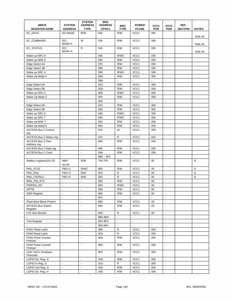
SMSC DS – LPC47N252 Page 130 Rev. 09/06/2000
MMCR
REGISTER NAME
SYSTEM
ADDRESS
SYSTEMADDRESS
TYPE
8051ADDRESS
(7F00+)8051TYPE
POWER
PLANEVCC1POR
VCC2POR
REF.
SECTION NOTES
EC_DATA ECI BASE R/W 53h R/W VCC1 00h Note 40
EC_COMMAND ECIBASE+4
W 53h R/W VCC1 00h Note 40
EC_STATUS ECIBASE+4
R 54h R/W VCC1 00h Note 40
Wake up SRC 8 - - 55h R/WC VCC1 00h -
Wake up MSK 8 - - 56h R/W VCC1 00h -
Edge Select 4A 57h R/W VCC1 00h
Edge Select 4B 58h R/W VCC1 00h
Wake up SRC 4 59h R/WC VCC1 00h
Wake Up Mask 4 5Ah R/W VCC1 00h
- - - 5Bh - - - -
Edge Select 5A 5Ch R/W VCC1 00h
Edge Select 5B 5Dh R/W VCC1 00h
Wake up SRC 5 5Eh R/WC VCC1 00h
Wake Up Mask 5 5Fh R/W VCC1 00h
- - - 60h - - - -
Edge Select 6A 61h R/W VCC1 00h
Edge Select 6B 62h R/W VCC1 00h
Wake up SRC 6 63h R/WC VCC1 00h
Wake up SRC 7 - - 64h R/WC VCC1 00h
Wake up MSK 7 - - 65h R/W VCC1 00h
Wake Up Mask 6 66h R/W VCC1 00h
ACCESS.Bus 2 Controlreg
- - 67h W VCC1 00h
ACCESS.Bus 2 Status reg - - 67h R VCC1 81h
ACCESS.Bus 2 OwnAddress reg
- - 68h R/W VCC1 00h
ACCESS.Bus 2 Data reg - - 69h R/W VCC1 00h
ACCESS.Bus 2 Clock - - 6Ah R/W VCC1 00h
- - - 6Bh – 6Fh - - - -
Mailbox registers[10-1F] MBX
A0-AF
R/W 70h-7Fh R/W VCC1 00 8
PM1_STS2 PM1+1 R/WC 80h R/W VCC1 00 8
PM1_EN2 PM1+3 R/W 81h R VCC1 00 8
PM1_CNTRL2 PM1+5 R/W 82h R VCC1 00 8
8051_PM_STS - - 83h R/W VCC1 00 -
PWRGD_INT - - 84h R/WC VCC1 00 -
GPTM - - 85h R/W VCC1 00 -
DMS Register - - 86h R/W VCC1 00 -
- - - 87h - - - -
Flash Boot Block Protect - - 88h R/W VCC1 00 -
ACCESS.Bus SwitchRegister
- - 89h R/W VCC1 03 -
LPC Bus Monitor - - 8Ah R VCC1 00 -
- - - 8Bh-8Dh - - - -
Test Register - - 8Eh-8Fh - - - -
- - - 90h-9Ah - - - -
FAN1 Read Latch - - 9Bh R VCC1 00h -
FAN2 Read Latch - - 9Ch R VCC1 00h -
FAN1 Pulse CounterPreload
- - 9Dh R/W VCC1 00h -
FAN2 Pulse CounterPreload
- - 9Eh R/W VCC1 00h -
FAN TACH TimebasePrescaler
9Fh R/W VCC1 05h -
LGPIO Dir. Reg. G - - A0h R/W VCC1 00h -
LGPIO In Reg. G - - A1h R VCC1 00h -
LGPIO Out Reg. G - - A2h R/W VCC1 00h -
LGPIO Dir. Reg. H - - A3h R/W VCC1 00h -

SMSC DS – LPC47N252 Page 131 Rev. 09/06/2000
MMCR
REGISTER NAME
SYSTEM
ADDRESS
SYSTEMADDRESS
TYPE
8051ADDRESS
(7F00+)8051TYPE
POWER
PLANEVCC1POR
VCC2POR
REF.
SECTION NOTES
LGPIO In Reg. H - - A4h R VCC1 00h -
LGPIO Out Reg. H - - A5h R/W VCC1 00h -
LGPIO Dir. Reg. I - - A6h R/W VCC1 00h -
LGPIO In Reg. I - - A7h R VCC1 00h -
LGPIO Out Reg. I - - A8h R/W VCC1 00h -
LGPIO LPC Select - - A9h R/W VCC1 00h -
LGPIO Buffer Type H - - AAh R/W VCC1 00h -
LGPIO Buffer Type I - - ABh R/W VCC1 00h -
GPIO Buffer Type - - ACh R/W VCC1 00h -
SGPIO Dir. Reg. J - - ADh R/W VCC1 00h -
SGPIO Dir. Reg. K - - AEh R/W VCC1 00h -
- - - AFh - - - - -
Flash High Address MBX9Fh R/W B0h R/W VCC1 00h -
Flash Low Address MBX80h R/W B1h R/W VCC1 00h -
Flash Data MBX81h R/W B2h R/W VCC1 00h -
- - - B3h-EFh - - - - -
256 bytes of RAM - - 7E00-7EFFh
R/W VCC1
Note 32: Although the Input and Output Data registers are physically separate, they share address 7FF1.
Note 33: The 8051 CPU cannot write to some bits of the Status register.
Note 34: Writing to the Auxiliary Output Data Register, loads the Output data register and can set the AUXOBF1output if enabled. This does not set the PCOBF output.
Note 35: Interrupt is cleared when read by the 8051.
Note 36: Interrupt is cleared when read by the host.
Note 37: These addresses are shared between the PS/2 Devil Logic and the SMSC PS/2 Hardware Channels A – D
Note 38: Bit 0 is the only writable or resetable bit in this register.
Note 39: VCC1 POR = 00000X10b, VCC2 POR = 00000X1Xb where X is not affected by VCC2 POR, but is left atthe current value.
Note 40: These registers have the same structure as the keyboard interface registers.
Note 41: The LPC RTC registers are relocatable and accessed by the 8051 through MMCRs 0x7FF5 – 0x7FF9.

SMSC DS – LPC47N252 Page 132 Rev. 09/06/2000
11.8.3 8051 CONFIGURATION/CONTROL MEMORY MAPPED REGISTERS
11.8.3.1 Disable Register
Table 102 - Disable RegisterHOST ADDRESS N/A
8051 ADDRESS 0x7F3F
POWER VCC1
DEFAULT 0x00
D7 D6 D5 D4 D3 D2 D1 D0
HOST TYPE - - - - - - - -
8051 TYPE R/W R/W R/W R/W R/W R/W R/W R/W
BIT NAME PARALLELPORT
SERIALPORT
IR PORT FLOPPYPORT
UD SYSTEMFLASH
RESERVED FORCEFDC
WRTPRT
PARALLEL PORT - When this bit is asserted ‘1’ the parallel port is enabled. When this bit is deasserted ‘0’ theparallel port is disabled.
SERIAL PORT - When this bit is asserted ‘1’ the Serial port is enabled. When this bit is deasserted ‘0’ the Serial portis disabled.
IR PORT - When this bit is asserted ‘1’ the IR port is enabled. When this bit is deasserted ‘0’ the IR port is disabled.
FLOPPY PORT - When this bit is asserted ‘1’ the Floppy Port is enabled. When this bit is deasserted ‘0’ the FloppyPort is disabled.
UD - The UD bit is User-Defined. UD bits are maintained by 8051 software, only.
SYSTEM FLASH - When the SYSTEM FLASH bit is asserted ‘1’, the LPC Host Flash programming interface isdisabled. When the SYSTEM FLASH bit is deasserted ‘0’, the LPC Host Flash programming interface is enabled(see section 13.5, LPC Bus Flash Program Access, on page 172.)
RESERVED - Logic ‘0’ read only access.
11.8.3.2 Device Rev Register
By reading this register, 8051 firmware can confirm the device revision that it is running on.
Table 103 - Device Rev RegisterHost N/A
8051 0x7F06
Power VCC1
Default 0x01
D7 D6 D5 D4 D3 D2 D1 D0
HOST TYPE - - - - - - - -
8051 TYPE R R R R R R R R
Bit description Current Revision 1
This register is hardwired. The current revision level is 1.

SMSC DS – LPC47N252 Page 133 Rev. 09/06/2000
11.8.3.3 Device ID Register
By reading this register, 8051 firmware can determine which device it is running on.
Table 104 - Device ID RegisterHost N/A
8051 0x7F07
Power VCC1
Default 0x0E
D7 D6 D5 D4 D3 D2 D1 D0
HOST TYPE - - - - - - - -
8051 TYPE R R R R R R R R
BIT DESCRIPTION 0 0 0 0 1 1 1 0
11.8.3.4 Configuration Register
Table 105 - Configuration Register 0Host N/A
8051 0x7FF4
Power VCC1
Default 0x00
D7 D6 D5 D4 D3 D2 D1 D0
HOST TYPE - - - - - - - -
8051 TYPE R/W R/W R/W R/W R/W R/W R/W R/W
BIT DESCRIPTION AUXH 0 OBFEN PS2_SEL MMC PCOBFEN SAEN SLEEPFLAG
AUXH - Aux in Hardware; when high, AUXOBF of the status register is set in hardware by a write to 7FFAh. Whenlow, AUXOBF of the status register is a user defined bit (UD) and R/W.
OBFEN - When set PCOBF is gated onto KIRQ and AUXOBF1 is gated onto MIRQ. When low, KIRQ and MIRQ aredriven low. Software should not change this bit when OBF of the status register is equal to 1.
MMC - Memory Map Control Bit : When MMC=0, a 256 Byte Scratch RAM area at 7D00h is available to the 8051.When MMC=1 the Scratch RAM at 7D00h-7DFFh becomes scratch ROM at 00h--FFh. When the MMC bit is ‘1’, theInternal Scratch RAM becomes Internal Scratch ROM and occupies 256 bytes at the top of the 64k code space; i.e.,FF00h – FFFFh (see section 13.2, Flash Program Interface Decoder 13.2. When the MMC bit is deasserted ‘0’, thereis 256 bytes of Internal Scratch RAM located at address 0x7D00 in the 8051 Data Space. When the MMC bit isasserted ‘1’, the 8051 can execute out of the Internal Scratch ROM either when the 8051 Code Fetch Accessinterface or when the 8051 Program Access interface is selected.
Note: When the 8051 is running from external flash, i.e. when the nEA pin = ‘0’, the MMC bit must be ‘0’.
PCOBFEN - When high, PCOBF reflects whatever value was written to the PCOBF firmware latch assigned to7FFDH. When low, PCOBF reflects the status of writes to 7FF1H (the output data register).
PS2_SELIf PS2_SEL=0 (default) then the PS2 Device Interface Logic (DEVIL) is enabled and if PS2_SEL=1 then the SMSCPS2 Interface (SPS2) is enabled. The following table illustrates this:
PS2_SEL INTERNAL ACTIVE PS/2 LOGIC BLOCK0 PS2 Device Interface Logic (DEVIL)1 SMSC PS2 Interface Logic (SPS2)

SMSC DS – LPC47N252 Page 134 Rev. 09/06/2000
SAENSoftware-assist enable. When set to “1” SAEN allows control of the GATEA20 signal via firmware. If SAEN is reset to‘0’, GATEA20 corresponds to either the last host-initiated control of GATEA20 or the firmware write to 7FFEh or7FFFh.
SLEEPFLAGIf SLEEPFLAG=“0” when PCON bit-0 is set, the 8051 enters “IDLE” mode, whereas if SLEEPFLAG=“1” when PCONbit 0 is set the 8051enters “SLEEP” mode. This bit is cleared by the occurrence of any wake-up events and onVCC1 POR.
11.8.3.5 Output Enable Register
Table 106 Output Enable RegisterHost N/A
8051 0x7F3E
Power VCC1
Default 00000X10b on VCC1 POR
00000X1Xb on VCC2 POR
Output Enable Register VCC1 POR = 0x00000X10, VCC2 POR = 00000X1Xb where X means the bit holds itssetting preceding VCC2 POR.
D7 - D4 D3 D2 D1 D0
HOST TYPE - - - - -
8051 TYPE R R/W R R/W R/W
BIT DESCRIPTION Reserved iRESET_
OVRD
POWER_
GOOD
iRESET_OUT 32kHz Output
iRESET_OUT - When POWER_GOOD = 1, iRESET_OUT is controlled by the 8051. When POWER_GOOD = 0,iRESET_OUT is forced high (within 100nsec) and latched. The nRESET_OUT pin is not driven until VCC2 is applied.iRESET_OUT cannot be cleared by the 8051 until POWER_GOOD =1.
See Note 42.
In the LPC47N252 , nRESET_OUT is driven high by this sequence of events.
Sets STP_CNT to a non-zero value
Clears iRESET_OUT bit, causing 8051STP_CLK bit 0 (see Table 209 page 15) to get set and STOP Counter to startdecrementing
When STP_CNT reaches 0 the nRESET_OUT pin deasserts (goes high) at which point the 8051’s clock stops.
POWER_GOOD - The Power_Good bit D2 reflects the state of the LPC47N252 Vcc2 Power Good pin PWRGD. ThePower_Good bit is read only.
iRESET_OVRD - iRESET Override - when cleared the iRESET_OUT bit functions as described above. When set,iRESET_OUT is given direct control over the internal reset and nRESET_OUT pins without requiring the STOP_CLKcounter or affecting the 8051STP_CLK bit. In the override mode, setting iRESET_OUT drives nRESET_OUT lowand clearing iRESET_OUT drives nRESET_OUT high.
The RESET_OUT Override function allows the 8051 to take the rest of the LPC47N252 chip (SIO) out of resetwithout giving up control (i.e., without stopping its clock).
Note: When the iRESET_OVRD bit is asserted the 8051 clock cannot be stopped.
Note 42: In the LPC47N252 iRESET Override mode is the typical mode of operation. When the iRESET_OVRD bit isasserted the 8051 clock cannot be stopped. Providing the mode to stop the 8051 clock is a legacy mode. To stopthe 8051 clock the iRESET_OVRD bit must be deasserted.
32 KHZ OUTPUT - The 32 kHz Output bit controls the LPC47N252 32 kHz_OUT . When 32kHz Output is ‘0’ the32kHz Output Clock is disabled and the 32 kHz_OUT pin is driven low. When 32 kHz Output is ‘1’ the 32 kHz OutputClock is enabled. The 32kHz Output bit is R/W and disabled by default following Vcc1 POR.

SMSC DS – LPC47N252 Page 135 Rev. 09/06/2000
11.8.3.6 8051 LPC Bus Monitor
The 8051 can monitor the state of the LPCPD# input pin using the LPCPD STATUS bit D0 in the LPC Bus Monitorregister (Table 107). The LPCPD STATUS bit is the inverse of the LPCPD# pin (see section 4.1.14 LPC PowerManagement for a description of the LPCPD# pin function).
When the LPCPD STATUS bit is ‘0’, the LPCPD# input pin is deasserted ‘1’. When the LPCPD STATUS bit is ‘1’, theLPCPD# input pin is asserted ‘0’.
Table 107 - LPC Bus Monitor RegisterHOST ADDRESS n/a
8051 ADDRESS 0x7F8A
POWER VCC1
DEFAULT ‘0000000X’b
D7 D6 D5 D4 D3 D2 D1 D0
HOST TYPE - - - - - - - -
8051 TYPE R R R R R R R R
BIT NAME Reserved LPCPD Status
Note: There is no LPCPD STATUS bit default.
11.8.4 LED CONTROLS
The LPC47N252 has three independent LED outputs that are programmable under 8051 control.
LED RegisterHost N/A
8051 0x7F21
Power VCC1
Default 0x00
D7 D6 D5 D4 D3 D2 D1 D0
Default 0 0 0 N/A 0 0 0 0
8051access
R/W R/W R/W R R/W R/W R/W R/W
Bit def FDDLed
Enable
FDD_LED1
FDD_LED0
status ofpin MODE
PWR_LED1
PWR_LED0
BAT_LED1
BAT_LED0
Note 1 00 FDD LED is off
01 LED flash; P=1.0sec10 LED flash; P=0.5sec11 LED is fully on
00 PWR LED is off
01 LED flash; P=3.0sec10 LED flash; P=1.5sec11 LED is fully on
00 Battery LED is off
01 LED flash; P=1.0sec10 LED flash; P=0.5sec11 LED is fully on
Note 1: D7 =1; FDD_LED Pin is controlled by D6, D5D7=0; FDD_LED is controlled by the Motor Enable 0 pin from the FDC. When Motor Enable 0 pin isasserted the LED is on.
LED on time is T=125msec; “0” is on, “1” is off. Period “P” is indicated above.

SMSC DS – LPC47N252 Page 136 Rev. 09/06/2000
P
T
FIGURE 13 - LED OUTPUT
11.9 8051 INTERRUPTS
The eleven 8051 core interrupts are shown described in Table 108 – 8051 Interrupts.
The 8051 has the following run time sources: int0, int1, int2, int3 and int4. The Interrupt sources of Int5_n create8051 Wakeup Events which are used to monitor and altar the power management state. There are three type ofsource triggers for wakeup event: Nonprogrammable (fixed edge), Selectable Edge (SE), Either Edge (EE).
The 8051 core has three interrupt priority levels: PFI, high and low. The PFI interrupt, if enabled, has priority over allother interrupts.
11.9.1 8051 INTERNAL PARALLEL INTERRUPTS
INT0 POL
TF0 POL
INT1 POL
RI + TI POL
TF2 POL
RESERVED
RESERVED
TF1 POL
0
1
2
3
4
5
6
7
0
1
2
3
4
5
6
7
0
1
2
3
4
5
6
7
WK_EE3 STAT
WK_EE2 STAT
WK_EE4 STAT
ACCBUS2 STAT
PS2_A/PS2 P1 STAT
PS2_B/PS2 P2 STAT
PS2_C STAT
PS2_D STAT
ANY WUP_MK
SYS-MBOX_MK
ACCBUS1_MK
EC_OBF_MK
EC_IBF_MK
KBD SCAN_MK
IBF_MK
GPIO3_MK
0
1
2
3
4
5
6
7
0
1
2
3
4
5
6
7
ANY WUP STAT
SYS-MBOX STA
ACCBUS1 STA
EC_OBF STAT
EC_IBF STAT
KBD SCAN STAT
IBF STAT
GPIO3 STAT
INT0 MASK (0x7F01)INT0 SRC (0x7F00)
Interrupt Polarity SFRInterrupt Enable SFR
INT0_EN
TF0_EN
INT1_EN
RI + TI_EN
TF2_EN
RESERVED
RESERVED
TF1_EN
INT1 MASK (0x7F03)INT1 SRC (0x7F02)
Note : WK_EE[2:4] are found at Wake Up register 2 and INT0 register.
GRP2
INT2
INT3_n
INT4
0
1
2
INT2INT3INT4
INT5_n3
External InterruptEnable SFR
PFI
POWER-FAIL EVENT
EICON SFR
GRP1
GRP1
IN2IN1IN0
0
1
2
3
4
5
6
7
nGPWKUP STAT
WK_ANYKEY ST
HTIMER STAT
WK_EE2 STAT
WK_EE4 STAT
UART_RI1 STAT
RESERVED
WK_EE3 STAT
RTC_ALRM MK
WK_EE1 MK
IR_RX MK
AB_DAT1 MK
PM1_STS_2 MK
PM1_EN 2 MK
PM1_CTL 2 MK
AB_DAT2 MK
0
1
2
3
4
5
6
7
0
1
2
3
4
5
6
7
RTC_ALRM STA
WK_EE1 STAT
IR_RX STAT
AB_DAT1 STAT
PM1_STS_2 STA
PM1_EN 2 STA
PM1_CTL 2 STA
AB_DAT2 STAT
Wake Up Src 2 (0x7F2B) Wake Up MSK 2 (0x7F2D)
Wake Up Src 1 (0x7F2A) Wake Up MSK 1 (0x7F2C)
nGPWKUP MK
WKANYKEY MK
HTIMER_MK
WK_EE2_MK
WK_EE4_MK
UART_RI1_MK
RESERVED
WK_EE3_MK
0
1
2
3
4
5
6
7
IN2IN1IN0
IN3
IN7
PGI0
PWRGD_INT (0x7F84)0
1
2
3
4
5
6
7
WK_EE3 MSK
WK_EE2 MSK
WK_EE4 MSK
ACCBUS2 MSK
PS2_A/PS2 P1 MSK
PS2_B/PS2 P2 MSK
PS2_C MSK
PS2_D MSK
0
1
2
3
4
5
6
7
TACH1 STAT
TACH2 STAT
FDC_PP STAT
RESERVED
RESERVED
RESERVED
RESERVED
RESERVED
Wake Up Src 7 (0x7F64) Wake Up MSK 7 (0x7F65)
TACH1 MSK
TACH2 MSK
FDC_PP MSK
RESERVED
RESERVED
RESERVED
RESERVED
RESERVED
0
1
2
3
4
5
6
7
0
1
2
3
4
5
6
7
LGPIO50 STAT
LGPIO51 STAT
LGPIO52 STAT
LGPIO54 STAT
LGPIO55 STAT
LGPIO56 STAT
LGPIO57 STAT
LGPIO53 STAT
Wake Up Src 8 (0x7F55) Wake Up MSK 8 (0x7F56)
LGPIO50 MSK
LGPIO51 MSK
LGPIO52 MSK
LGPIO54 MSK
LGPIO55 MSK
LGPIO56 MSK
LGPIO57 MSK
LGPIO53 MSK
0
1
2
3
4
5
6
7
8/27/99
FIGURE 14 - 8051 INTERRUPTS

SMSC DS – LPC47N252 Page 137 Rev. 09/06/2000
0
1
2
3
4
5
6
7
WK_SE00_MK0
WK_SE01_MK1
WK_SE02_MK2
WK_SE03_MK3
WK_SE04_MK4
WK_SE05_MK
WK_SE06_MK6
WK_SE07_MK7
Wake Up SRC 4 (0x____) Wake Up MSK 4 (0x____)
5
Edge Select 4 (0x____)
WK_SE00_SRC
WK_SE01_SRC
WK_SE02_SRC
WK_SE03_SRC
WK_SE04_SRC
WK_SE05_SRC
WK_SE06_SRC
WK_SE07_SRC
WK_SE00_SEL
WK_SE01_SEL
WK_SE02_SEL
WK_SE03_SEL
WK_SE04_SEL
WK_SE05_SEL
WK_SE06_SEL
WK_SE07_SEL
0
1
2
3
4
5
6
7
WK_SE10_MK0
WK_SE11_MK1
WK_SE12_MK2
WK_SE13_MK3
WK_SE14_MK4
WK_SE15_MK
WK_SE16_MK6
WK_SE17_MK7
Wake Up SRC 5 (0x____) Wake Up MSK 5 (0x____)
5
Edge Select 5 (0x____)
WK_SE10_SRC
WK_SE11_SRC
WK_SE12_SRC
WK_SE13_SRC
WK_SE14_SRC
WK_SE15_SRC
WK_SE16_SRC
WK_SE17_SRC
WK_SE10_SEL
WK_SE11_SEL
WK_SE12_SEL
WK_SE13_SEL
WK_SE14_SEL
WK_SE15_SEL
WK_SE16_SEL
WK_SE17_SEL
0
1
2
3
4
5
6
7
WK_SE20_MK0
WK_SE21_MK1
WK_SE22_MK2
WK_SE23_MK3
WK_SE24_MK4
WK_SE25_MK
WK_SE26_MK6
WK_SE27_MK7
Wake Up SRC 6 (0x____) Wake Up MSK 6 (0x____)
5
Edge Select 6 (0x____)
WK_SE20_SRC
WK_SE21_SRC
WK_SE22_SRC
WK_SE23_SRC
WK_SE24_SRC
WK_SE25_SRC
WK_SE26_SRC
WK_SE27_SRC
WK_SE20_SEL
WK_SE21_SEL
WK_SE22_SEL
WK_SE23_SEL
WK_SE24_SEL
WK_SE25_SEL
WK_SE26_SEL
WK_SE27_SEL
0,1
2,3
4,5
6,7
0,1
2,3
4,5
6,7
0,1
2,3
4,5
6,7
0,1
2,3
4,5
6,7
0,1
2,3
4,5
6,7
0,1
2,3
4,5
6,7
IN4IN5
GPIO0GPIO1GPIO2
IN6GPIO7GPIO4
GPIO5GPIO6GPIO8GPIO9
GPIO10GPIO11GPIO12GPIO13
GPIO14GPIO15GPIO16GPIO17GPIO19GPIO20GPIO21GPIO18
INT2
INT3
INT4
GRP2
FIGURE 15 – EXTENDED INTERRUPTS & WAKE EVENTS
Note: Wake events apply per pin and are available to all functions of that pin. For example, if the IRRX function isselected as an alternate function of the GPIO8 pin (MISC7 = 1), the WK_SE12 event can be used for IR wake-up.See Section 15.3, Wake-up Events on page 191.
Table 108 – 8051 Interrupts
INTERRUPT DESCRIPTIONNATURALPRIORITY FLAG ENABLE
PRIORITYCONTROL
INTERRUPTVECTOR
pfi Power Fail Interrupt 0 EICON.4 EICON.5 n/a 0x33
int0_n External Interrupt 0 1 TCON.1 IE.0 IP.0 0x03
TF0 Timer 0 Interrupt 2 TCON.5 IE.1 IP.1 0x0B
int1_n External Interrupt 1 3 TCON.3 IE.2 IP.2 0x13
TF1 Timer 1 Interrupt 4 TCON.7 IE.3 IP.3 0x1B
TI_0 or RI_0 Serial Port 0 Transmitor Receive
5 SCON0.0 (RI_0),
SCON0.1 (RI_0)
IE.4 IP.4 0x23
TF2 or EXF2 Timer 2 Interrupt 6 T2CON.7 (TF2),T2CON.6 (EXF2)
IE.5 IP.5 0x2B
RESERVED 7 RESERVED IE.6 IP.6 0x3B
int2 External Interrupt 2 8 EXIF.4 EIE.0 EIP.0 0x43
int3_n (1) External Interrupt 3 9 EXIF.5 EIE.1 EIP.1 0x4B
int4 External Interrupt 4 10 EXIF.6 EIE.2 EIP.2 0x53
int5_n External Interrupt 5 11 EXIF.7 EIE.3 EIP.3 0x5B
RESERVED 12 EICON.3 EIE.4 EIP.4 0x63
Note: The int5_n interrupt is used to restart the 8051 from sleep mode. This interrupt includes the interrupt WAKEUP sources from GRP1 and Grp2 on FIGURE 14 and FIGURE 15.

SMSC DS – LPC47N252 Page 138 Rev. 09/06/2000
11.9.2 8051 INT0 SOURCE REGISTER
The eight interrupts in the INT0 Source register (Table 109 ) are logically ‘OR’ed to drive the 8051 int0_n interrupt(FIGURE 14). When any bit in the INT0 Source register is ‘1’, an interrupt has occurred and, assuming the interruptis enabled, the 8051 int0_n input is asserted.
The bits in the INT0 Source register are cleared by a writing a “1” to the bit.
Table 109 - 8051 Int0 Source RegisterHOST ADDRESS N/A
8051 ADDRESS 0x7F00
POWER VCC1
DEFAULT 0x00
D7 D6 D5 D4 D3 D2 D1 D0
HOST TYPE - - - - - - - -
8051 TYPE R/WC R/WC R/WC R/WC R/WC R/WC R/WC R/WC
BIT NAME PS2_D PS2_C PS2_B/
PS2 P2
PS2_A/
PS2 P1
ACCESSBUS 2
WK_EE4 WK_EE2 WK_EE3
SMSC PS/2 C & D Interrupts – D[7:6]INT0 Source register bit D7 is the SMSC PS/2 Channel D interrupt; INT0 Source register bit D6 is the SMSC PS/2Channel C interrupt. These interrupts are active when the PS2_SEL Control bit D4 in Configuration Register 0(0x7FF4) is ‘1.’ The Configuration Register 0 register is described in the section see 11.8.3.4.
When the SMSC PS/2 channels are active the PS2_D interrupt is associated with the PS2CLK and PS2DATalternate functions of the GPIO20 and GPIO21 pins; PS2_C is associated with the IMCLK and IMDATA pins.
Dual-Mode SMSC/DEVIL Interrupts – D[5:4]INT0 Source register bits D5 and D4 are multiplexed between the SMSC PS/2 Channels A and B and the Devil LogicPorts P1 and P2.
When the PS2_SEL Control bit D4 in Configuration Register 0 (0x7FF4) is ‘1,’ the SMSC PS/2 Interrupt Channels Aand B are selected; when PS2_SEL = ‘0,’ the Devil Logic Ports P1 and P2 are selected.
When the SMSC PS/2 channels are active the PS2_B interrupt is associated with the KCLK and KDAT pins; PS2_Ais associated with the EMCLK and EMDATA pins.
Access Bus 2 Interrupt – D3“1” Indicates an ACCESS.Bus 2 interrupt is active.
WK_EE[4:2] – D2, D0, D1ACCESS Bus 2 wake events can be generated. AB_DAT ACCESS BUS 2 bit in Wake Sources Register 1. 8051INT0 Mask Register The eight interrupts in the INT0 Source register (Table 109) are enabled by bits of the samename in the INT0 Mask register (Table 110).
When any bit in the INT0 Mask register is ‘0’, the interrupt is enabled. When any bit in the INT0 Mask register is ‘1,the interrupt is masked. When masked interrupts are asserted, the interrupt will be visible in the interrupt sourceregister but will not assert an interrupt to the 8051.
The bits in the INT0 Mask register are read/write. The INT0 interrupts are enabled by default.
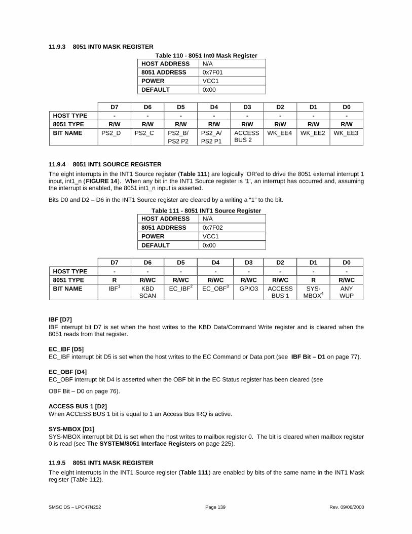
SMSC DS – LPC47N252 Page 139 Rev. 09/06/2000
11.9.3 8051 INT0 MASK REGISTER
Table 110 - 8051 Int0 Mask RegisterHOST ADDRESS N/A
8051 ADDRESS 0x7F01
POWER VCC1
DEFAULT 0x00
D7 D6 D5 D4 D3 D2 D1 D0
HOST TYPE - - - - - - - -
8051 TYPE R/W R/W R/W R/W R/W R/W R/W R/W
BIT NAME PS2_D PS2_C PS2_B/PS2 P2
PS2_A/PS2 P1
ACCESSBUS 2
WK_EE4 WK_EE2 WK_EE3
11.9.4 8051 INT1 SOURCE REGISTER
The eight interrupts in the INT1 Source register (Table 111) are logically ‘OR’ed to drive the 8051 external interrupt 1input, int1_n (FIGURE 14). When any bit in the INT1 Source register is ‘1’, an interrupt has occurred and, assumingthe interrupt is enabled, the 8051 int1_n input is asserted.
Bits D0 and D2 – D6 in the INT1 Source register are cleared by a writing a “1” to the bit.
Table 111 - 8051 INT1 Source RegisterHOST ADDRESS N/A
8051 ADDRESS 0x7F02
POWER VCC1
DEFAULT 0x00
D7 D6 D5 D4 D3 D2 D1 D0
HOST TYPE - - - - - - - -
8051 TYPE R R/WC R/WC R/WC R/WC R/WC R R/WC
BIT NAME IBF1 KBDSCAN
EC_IBF2 EC_OBF3 GPIO3 ACCESSBUS 1
SYS-MBOX4
ANYWUP
IBF [D7]IBF interrupt bit D7 is set when the host writes to the KBD Data/Command Write register and is cleared when the8051 reads from that register.
EC_IBF [D5]EC_IBF interrupt bit D5 is set when the host writes to the EC Command or Data port (see IBF Bit – D1 on page 77).
EC_OBF [D4]EC_OBF interrupt bit D4 is asserted when the OBF bit in the EC Status register has been cleared (see
OBF Bit – D0 on page 76).
ACCESS BUS 1 [D2]When ACCESS BUS 1 bit is equal to 1 an Access Bus IRQ is active.
SYS-MBOX [D1]SYS-MBOX interrupt bit D1 is set when the host writes to mailbox register 0. The bit is cleared when mailbox register0 is read (see The SYSTEM/8051 Interface Registers on page 225).
11.9.5 8051 INT1 MASK REGISTER
The eight interrupts in the INT1 Source register (Table 111) are enabled by bits of the same name in the INT1 Maskregister (Table 112).
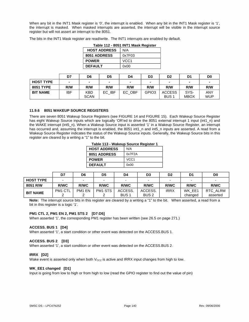
SMSC DS – LPC47N252 Page 140 Rev. 09/06/2000
When any bit in the INT1 Mask register is ‘0’, the interrupt is enabled. When any bit in the INT1 Mask register is ‘1’,the interrupt is masked. When masked interrupts are asserted, the interrupt will be visible in the interrupt sourceregister but will not assert an interrupt to the 8051.
The bits in the INT1 Mask register are read/write. The INT1 interrupts are enabled by default.
Table 112 - 8051 INT1 Mask RegisterHOST ADDRESS N/A
8051 ADDRESS 0x7F03
POWER VCC1
DEFAULT 0x00
D7 D6 D5 D4 D3 D2 D1 D0
HOST TYPE - - - - - - - -
8051 TYPE R/W R/W R/W R/W R/W R/W R/W R/W
BIT NAME IBF KBDSCAN
EC_IBF EC_OBF GPIO3 ACCESSBUS 1
SYS-MBOX
ANYWUP
11.9.6 8051 WAKEUP SOURCE REGISTERS
There are seven 8051 Wakeup Source Registers (see FIGURE 14 and FIGURE 15). Each Wakeup Source Registerhas eight Wakeup Source inputs which are logically ‘OR’ed to drive the 8051 external interrupt 1 input (int1_n) andthe WAKE interrupt (int5_n). When a Wakeup Source input is asserted ‘1’ in a Wakeup Source Register, an interrupthas occurred and, assuming the interrupt is enabled, the 8051 int1_n and int5_n inputs are asserted. A read from aWakeup Source Register indicates the status of the Wakeup Source inputs. Generally, the Wakeup Source bits in thisregister are cleared by a writing a “1” to the bit.
Table 113 - Wakeup Source Register 1HOST ADDRESS N/A
8051 ADDRESS 0x7F2A
POWER VCC1
DEFAULT 0x00
D7 D6 D5 D4 D3 D2 D1 D0
HOST TYPE - - - - - - - -
8051 R/W R/WC R/WC R/WC R/WC R/WC R/WC R/WC R/WC
BIT NAMEPM1 CTL
2PM1 EN
2PM1 STS
2ACCESS.
BUS 1ACCESS.
BUS 2IRRX WK_EE1
changedRTC_ALRM
asserted
Note: The interrupt source bits in this register are cleared by a writing a “1” to the bit. When asserted, a read from abit in this register is a logic ‘1’.
PM1 CTL 2, PM1 EN 2, PM1 STS 2 [D7:D5]When asserted ‘1’, the corresponding PM1 register has been written (see 26.5 on page 271.)
ACCESS. BUS 1 [D4]When asserted ‘1’, a start condition or other event was detected on the ACCESS.BUS 1.
ACCESS. BUS 2 [D3]When asserted ‘1’, a start condition or other event was detected on the ACCESS.BUS 2.
IRRX [D2]Wake event is asserted only when both VCC2 is active and IRRX input changes from high to low.
WK_EE1 changed [D1]Input is going from low to high or from high to low (read the GPIO register to find out the value of pin)
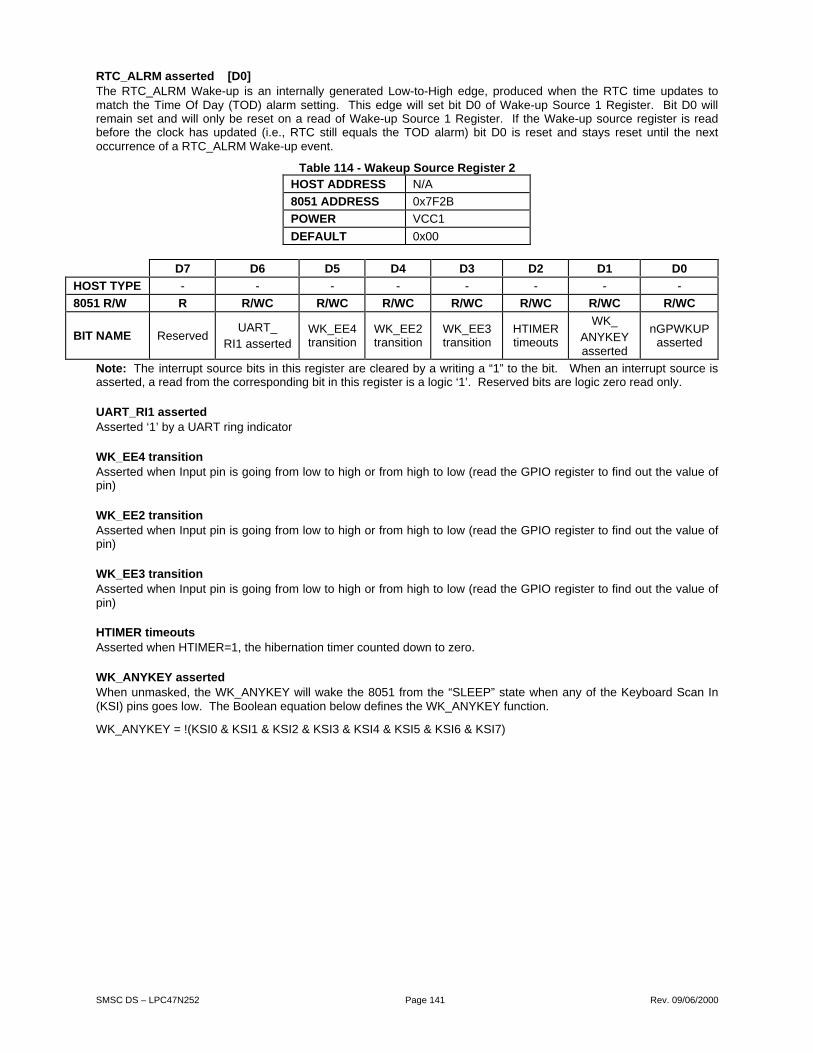
SMSC DS – LPC47N252 Page 141 Rev. 09/06/2000
RTC_ALRM asserted [D0]The RTC_ALRM Wake-up is an internally generated Low-to-High edge, produced when the RTC time updates tomatch the Time Of Day (TOD) alarm setting. This edge will set bit D0 of Wake-up Source 1 Register. Bit D0 willremain set and will only be reset on a read of Wake-up Source 1 Register. If the Wake-up source register is readbefore the clock has updated (i.e., RTC still equals the TOD alarm) bit D0 is reset and stays reset until the nextoccurrence of a RTC_ALRM Wake-up event.
Table 114 - Wakeup Source Register 2HOST ADDRESS N/A
8051 ADDRESS 0x7F2B
POWER VCC1
DEFAULT 0x00
D7 D6 D5 D4 D3 D2 D1 D0
HOST TYPE - - - - - - - -
8051 R/W R R/WC R/WC R/WC R/WC R/WC R/WC R/WC
BIT NAME ReservedUART_
RI1 assertedWK_EE4transition
WK_EE2transition
WK_EE3transition
HTIMERtimeouts
WK_ANYKEYasserted
nGPWKUPasserted
Note: The interrupt source bits in this register are cleared by a writing a “1” to the bit. When an interrupt source isasserted, a read from the corresponding bit in this register is a logic ‘1’. Reserved bits are logic zero read only.
UART_RI1 assertedAsserted ‘1’ by a UART ring indicator
WK_EE4 transitionAsserted when Input pin is going from low to high or from high to low (read the GPIO register to find out the value ofpin)
WK_EE2 transitionAsserted when Input pin is going from low to high or from high to low (read the GPIO register to find out the value ofpin)
WK_EE3 transitionAsserted when Input pin is going from low to high or from high to low (read the GPIO register to find out the value ofpin)
HTIMER timeoutsAsserted when HTIMER=1, the hibernation timer counted down to zero.
WK_ANYKEY assertedWhen unmasked, the WK_ANYKEY will wake the 8051 from the “SLEEP” state when any of the Keyboard Scan In(KSI) pins goes low. The Boolean equation below defines the WK_ANYKEY function.
WK_ANYKEY = !(KSI0 & KSI1 & KSI2 & KSI3 & KSI4 & KSI5 & KSI6 & KSI7)

SMSC DS – LPC47N252 Page 142 Rev. 09/06/2000
nGPWKUP assertedTable 115 - Wakeup Source Register 4
HOST ADDRESS N/A
8051 ADDRESS 0x7F59
POWER VCC1
DEFAULT 0x00
D7 D6 D5 D4 D3 D2 D1 D0
HOST TYPE - - - - - - - -
8051 R/W R/WC R/WC R/WC R/WC R/WC R/WC R/WC R/WC
BIT NAMEWK_SE07asserted
WK_SE06asserted
WK_SE05asserted
WK_SE04asserted
WK_SE03asserted
WK_SE02asserted
WK_SE01asserted
WK_SE00asserted
Note: The interrupt source bits in this register are cleared by a writing a “1” to the bit. When an interrupt source isasserted, a read from the corresponding bit in this register is a logic ‘1’.
Table 116 - Wakeup Source Register 5HOST ADDRESS N/A
8051 ADDRESS 0x7F5E
POWER VCC1
DEFAULT 0x00
D7 D6 D5 D4 D3 D2 D1 D0
HOST TYPE - - - - - - - -
8051 R/W R/WC R/WC R/WC R/WC R/WC R/WC R/WC R/WC
BIT NAME WK_SE17asserted
WK_SE16asserted
WK_SE15asserted
WK_SE14asserted
WK_SE13asserted
WK_SE12asserted
WK_SE11asserted
WK_SE10asserted
Note: The interrupt source bits in this register are cleared by a writing a “1” to the bit. When an interrupt source isasserted, a read from the corresponding bit in this register is a logic ‘1’.
Table 117 - Wakeup Source Register 6HOST ADDRESS N/A
8051 ADDRESS 0x7F63
POWER VCC1
DEFAULT 0x00
D7 D6 D5 D4 D3 D2 D1 D0
HOST TYPE - - - - - - - -
8051 R/W R/WC R/WC R/WC R/WC R/WC R/WC R/WC R/WC
BIT NAME WK_SE17asserted
WK_SE16asserted
WK_SE15asserted
WK_SE14asserted
WK_SE13asserted
WK_SE12asserted
WK_SE11asserted
WK_SE10asserted
Note: The interrupt source bits in this register are cleared by a writing a “1” to the bit. When an interrupt source isasserted, a read from the corresponding bit in this register is a logic ‘1’.

SMSC DS – LPC47N252 Page 143 Rev. 09/06/2000
Table 118 - Wakeup Source Register 7HOST ADDRESS N/A
8051 ADDRESS 0x7F64
POWER VCC1
DEFAULT 0x00
D7 D6 D5 D4 D3 D2 D1 D0
HOST TYPE - - - - - - - -
8051 TYPE R R R R R R/WC R/WC R/WC
BIT NAMERESERVED FDC_PP
(Either-Edge)
FANTACH2
FAN TACH1
Note: The interrupt source bits in this register are cleared by a writing a “1” to the bit. When an interrupt source isasserted, a read from the corresponding bit in this register is a logic ‘1’. Reserved bits are logic zero read only.
Table 119 - Wakeup Source Register 8HOST ADDRESS N/A
8051 ADDRESS 0x7F55
POWER VCC1
DEFAULT 0x00
D7 D6 D5 D4 D3 D2 D1 D0
HOST TYPE - - - - - - - -
8051 TYPE R/WC R/WC R/WC R/WC R/WC R/WC R/WC R/WC
BIT NAME LGPIO57 LGPIO56 LGPIO55 LGPIO54 LGPIO53 LGPIO52 LGPIO51 LGPIO50
Note: The interrupt source bits in this register are cleared by a writing a “1” to the bit. When an interrupt source isasserted, a read from the corresponding bit in this register is a logic ‘1’.
11.9.7 8051 WAKEUP MASK REGISTERS
There are seven 8051 Wakeup Mask Registers with Mask bits which correspond to the Wakeup Source Registers(FIGURE 14 and FIGURE 15 ). When a bit in a Wakeup Mask Register is asserted ‘1’, the corresponding WakeupSource interrupt is masked. When a bit in a Wakeup Mask Register is deasserted ‘0’, the corresponding WakeupSource interrupt is enabled. When masked interrupts are asserted, the interrupt can be read in the Wakeup SourceRegister but will not assert an interrupt to the 8051. The Wakeup Mask Registers are read/write access. All Wakeupinterrupts are enabled by default.
Table 120 - Wakeup Mask Register 1HOST ADDRESS N/A
8051 ADDRESS 0x7F2C
POWER VCC1
DEFAULT 0x00
D7 D6 D5 D4 D3 D2 D1 D0
HOST TYPE - - - - - - - -
8051 R/W R/W R/W R/W R/W R/W R/W R/W R/W
BIT NAME PM1 CTL 2 PM1 EN 2 PM1 STS 2ACCESS.
BUS 1ACCESS.
BUS 2IRRX WK_EE1 RTC_ALRM
Note: When set ‘1’, a bit in this register masks the corresponding bit in Table 113 - Wakeup Source Register 1.

SMSC DS – LPC47N252 Page 144 Rev. 09/06/2000
Table 121 - Wakeup Mask Register 2HOST ADDRESS N/A
8051 ADDRESS 0x7F2D
POWER VCC1
DEFAULT 0x00
D7 D6 D5 D4 D3 D2 D1 D0
HOST TYPE - - - - - - - -
8051 R/W R R/W R/W R/W R/W R/W R/W R/W
BIT NAME Reserved UART_
RI1
WK_EE4 WK_EE2 WK_EE3 HTIMERtimeouts
WK_
ANYKEY asserted
nGPWKUPasserted
Note: When set ‘1’, a bit in this register masks the corresponding bit in Table 114 - Wakeup Source Register 2.Reserved bits are logic zero read only.
Table 122 - Wakeup Mask Register 4HOST ADDRESS N/A
8051 ADDRESS 0x7F5A
POWER VCC1
DEFAULT 0x00
D7 D6 D5 D4 D3 D2 D1 D0
HOST TYPE - - - - - - - -
8051 R/W R/WC R/WC R/WC R/WC R/WC R/WC R/WC R/WC
BIT NAME WK_SE07 WK_SE06 WK_SE05 WK_SE04 WK_SE03 WK_SE02 WK_SE01 WK_SE00Note: When set ‘1’, a bit in this register masks the corresponding bit in Table 115 - Wakeup Source Register 4.
Table 123 - Wakeup Mask Register 5HOST ADDRESS N/A
8051 ADDRESS 0x7F5F
POWER VCC1
DEFAULT 0x00
D7 D6 D5 D4 D3 D2 D1 D0
HOST TYPE - - - - - - - -
8051 R/W R/WC R/WC R/WC R/WC R/WC R/WC R/WC R/WC
BIT NAME WK_SE17 WK_SE16 WK_SE15 WK_SE14 WK_SE13 WK_SE12 WK_SE11 WK_SE10
Note: When set ‘1’, a bit in this register masks the corresponding bit Table 116 - Wakeup Source Register 5.User Note: An edge-sensitive IR wake-up scheme like in the LPC47N252 is susceptible to noise from externaldevices such as florescent lighting, etc. There are no provisions for digitally filtering this input. An external switchedfilter may be required to minimize noise.
Table 124 - Wakeup Mask Register 6HOST ADDRESS N/A
8051 ADDRESS 0x7F66
POWER VCC1
DEFAULT 0x00
D7 D6 D5 D4 D3 D2 D1 D0
HOST TYPE - - - - - - - -
8051 R/W R/WC R/WC R/WC R/WC R/WC R/WC R/WC R/WC
BIT NAME WK_SE27 WK_SE26 WK_SE25 WK_SE24 WK_SE23 WK_SE22 WK_SE21 WK_SE20
Note: When set ‘1’, a bit in this register masks the corresponding bit in Table 124 - Wakeup Mask Register 6.

SMSC DS – LPC47N252 Page 145 Rev. 09/06/2000
Table 125 - Wakeup Mask Register 7HOST ADDRESS N/A
8051 ADDRESS 0x7F65
POWER VCC1
DEFAULT 0x00
D7 D6 D5 D4 D3 D2 D1 D0
HOST TYPE - - - - - - - -
8051 TYPE R R R R R R/W R/W R/W
BIT NAME RESERVED FDC_PP FAN TACH2 FAN TACH1
Note: When set ‘1’, a bit in this register masks the corresponding bit in Table 118 - Wakeup Source Register 7.
Table 126 - Wakeup Mask Register 8HOST ADDRESS N/A
8051 ADDRESS 0x7F56
POWER VCC1
DEFAULT 0x00
D7 D6 D5 D4 D3 D2 D1 D0
HOST TYPE - - - - - - - -
8051 TYPE R/W R/W R/W R/W R/W R/W R/W R/W
BIT NAME LGPIO57 LGPIO56 LGPIO55 LGPIO54 LGPIO53 LGPIO52 LGPIO51 LGPIO50
Note: When set ‘1’, a bit in this register masks the corresponding bit in Table 119 - Wakeup Source Register 8.
11.9.8 8051 HIBERNATION TIMER REGISTER
Table 127 - HTIMER RegisterHOST ADDRESS N/A
8051 ADDRESS 0x7FF3
POWER VCC1
DEFAULT 0x00
Hibernation Timer - This 8 bit binary count-down timer can be programmed for from 30 seconds to 128 minutes in30 second increments. When it expires (reaches “0”), it stops (remains at “0”) and causes a hardware event that willwake up the 8051. This timer is clocked by the 32 KHz clock and is powered by VCC1. Writing a non-zero value tothis register starts the counter from that value.
11.9.9 8051 EDGE SELECT REGISTERS
Selectable Edge interrupts
Selectable interrupts SE00-SE07 are on External INT2.
Selectable interrupts SE10-SE17 are on External INT3.
Selectable interrupts SE20-SE27 are on External INT4.

SMSC DS – LPC47N252 Page 146 Rev. 09/06/2000
Table 128 - Edge Select 4AHOST ADDRESS N/A
8051 ADDRESS 0x7F57
POWER VCC1
DEFAULT 0x00
D7:6 D5:4 D3:2 D1:0
HOST TYPE - - - -
8051 R/W R/W R/W R/W R/W
BIT NAME SE03 Select SE02 Select SE01 Select SE00 Select
User Note: Edge-generated interrupts may occur from a change in the edge select bits.
Table 129 - Edge Selection
Edge Selection TableD7:6D5:4
D3:2D1:0
Edge High to low 00
Edge Low to High 01
Either Edge 10
Reserved 11
Table 130 - Edge Select 4BHOST ADDRESS N/A
8051ADDRESS 0x7F58
POWER VCC1
DEFAULT 0x00
D7:6 D5:4 D3:2 D1:0
HOST TYPE - - - -
8051 R/W R/W R/W R/W R/W
BIT NAME ANDDESCRIPTION
SE07 Select SE06 Select SE05 Select SE04 Select
User Note: Edge-generated interrupts may occur from a change in the edge select bits.
Refer to Table 129 - Edge Selection for the edge selection table.
Table 131 - Edge Select 5AHOST ADDRESS N/A
8051 ADDRESS 0x7F5C
POWER VCC1
DEFAULT 0x00
D7:6 D5:4 D3:2 D1:0
HOST TYPE - - - -
8051 R/W R/W R/W R/W R/W
BIT NAME SE13 Select SE12 Select SE11 Select SE10 Select
User Note: Edge-generated interrupts may occur from a change in the edge select bits.
Refer to Table 129 for the edge selection table.

SMSC DS – LPC47N252 Page 147 Rev. 09/06/2000
Table 132 - Edge Select 5BHOST ADDRESS N/A
8051 ADDRESS 0x7F5D
POWER VCC1
DEFAULT 0x00
D7:6 D5:4 D3:2 D1:0
HOST TYPE - - - -
8051 R/W R/W R/W R/W R/W
BIT NAME SE17 Select SE16 Select SE15 Select SE14 Select
User Note: Edge-generated interrupts may occur from a change in the edge select bits.
Refer to Table 129 for the edge selection table.
Table 133 - Edge Select 6AHOST ADDRESS N/A
8051 ADDRESS 0x7F61
POWER VCC1
DEFAULT 0x00
D7:6 D5:4 D3:2 D1:0
HOST TYPE - - - -
8051 R/W R/W R/W R/W R/W
BIT NAME SE23 Select SE22 Select SE21 Select SE20 Select
User Note: Edge-generated interrupts may occur from a change in the edge select bits.
Refer to Table 129 for the edge selection table.
Table 134 - Edge Select 6BHOST ADDRESS N/A
8051 ADDRESS 0x7F62
POWER VCC1
DEFAULT 0x00
D7:6 D5:4 D3:2 D1:0
HOST TYPE - - - -8051 R/W R/W R/W R/W R/WBIT NAME ANDDESCRIPTION
SE27 Select SE26 Select SE25 Select SE24 Select
User Note: Edge-generated interrupts may occur from a change in the edge select bits.
Refer to Table 129 for the edge selection table.
11.9.10 POWER FAIL IRQ
The PWRGD_INT register (Table 135) contains the Power Good Interrupt (PGI) bit, D0. When PGI = ‘1’, the (VCC2)PWRGD input has been deasserted; otherwise, PGI = ‘0’. Note: PGI is not asserted when PWRGD is asserted.
The PGI bit is the source for the high-performance 8051 Power Fail Interrupt (pfi) input (FIGURE 14). The VCC2power fail detect function is implemented as described in 8051 RING OSCILLATOR FAIL-SAFE CONTROLS onpage 125.
The PGI bit is readable and is cleared by writing a ‘1’ to D0 in the PWRGD_INT register.

SMSC DS – LPC47N252 Page 148 Rev. 09/06/2000
Table 135 - Power Good Interrupt Register (PWRGD_INT)HOST ADDRESS 8051 ADDRESS POWER PLANE DEFAULT
- 0x7F84 VCC1 0x00
D7 D6 D5 D4 D3 D2 D1 D0
HOST TYPE - - - - - - - -
8051 TYPE R R R R R R R R/WC
BIT NAME RESERVED PGI
11.9.11 8051 EXTERNAL SERIAL IRQ GENERATION
The 8051 can assert an interrupt on the serial IRQ stream to support software-generated SCI, SMI, or PME events(FIGURE 16). The 8051 External Serial IRQ interface is controlled by the 8051_SIRQ register (Table 136).
Note: The 8051 External Serial IRQ is generated and cleared by software.
IRQ Mappinglogic
SerialIRQ
8051_IRQ
8051_IRQ SELECT
FIGURE 16 - 8051 EXTERNAL SERIAL IRQ BLOCK DIAGRAM
Table 136 - 8051_SIRQ RegisterHOST ADDRESS 8051 ADDRESS POWER PLANE DEFAULT
- 0x7F52 VCC1 0x00
D7 D6 D5 D4 D3 D2 D1 D0
HOST TYPE - - - - - - - -
8051 TYPE R/W R/W R/W R/W R/W R/W R R
BIT NAME 8051_IRQ SELECT 8051_IRQ
ENABLE
8051_IRQ RESERVED
8051_IRQ SELECTFour bits that selects which IRQ is utilized when an interrupt occurs. See Table 137 – 8051 IRQ Mapping ControlBits.
8051_IRQ ENABLEThis bit must be set to one in order for an interrupt to occur.
8051 IRQThis bit must set to one in order for the 8051 to assert the mapped interrupt request corresponding to the 8051_IRQSELECT bits. The defualt state for a disabled IRQ is asserted.
Table 137 - 8051 IRQ Mapping Control Bits8051_IRQ ENABLE 8051_IRQ SELECT DESCRIPTION
0 XXXX DISABLED
1 0000 NO INTERRUPT
1 0001 MAP TO IRQ1
1 0010 MAP TO IRQ2
1 0011 MAP TO IRQ3
1 0100 MAP TO IRQ4

SMSC DS – LPC47N252 Page 149 Rev. 09/06/2000
8051_IRQ ENABLE 8051_IRQ SELECT DESCRIPTION
1 0101 MAP TO IRQ5
1 0110 MAP TO IRQ6
1 0111 MAP TO IRQ7
1 1000 MAP TO IRQ8
1 1001 MAP TO IRQ9
1 1010 MAP TO IRQ10
1 1011 MAP TO IRQ11
1 1100 MAP TO IRQ12
1 1101 MAP TO IRQ13
1 1110 MAP TO IRQ14
1 1111 MAP TO IRQ15
11.10 8051 CODE DEBUGGING FEATURES
The Kahuna 8051 code debugging facilities include an external Flash interface, the 8051-controlled parallel portinterface and the 8051-controlled UART. Other capabilities include the 8051 single-step capabilities and the SFR-driven GPIO pins.
11.10.1 EXTERNAL FLASH INTERFACE
The Kahuna External Flash Interface enables the read-only portion of the internal 8051 program memory bus toaccess an external ROM device using the KBD Scan interface pins. For a detailed description of the External FlashInterface see section 13.7 External Flash Interface on page 175.
11.10.2 8051-CONTROLLED PARALLEL PORT INTERFACE
The 8051-controlled Parallel Port Interface (PPPI 8051 mode) allows the 8051 to control the Kahuna parallel port pinsusing a set of three on-chip memory-mapped control registers. The 8051-controlled Parallel Port Interface can beused during program code development for diagnostic print functions. For a description of the 8051- controlledParallel Port Interface see section 9.3.1, PPPI 8051 Mode on page 112.
11.10.3 8051 SERIAL PORT
The 8051 serial port can be used during program code development for diagnostic functions. The 8051 serial portpins 8051TX and 8051RX are available on VCC1.
11.10.4 8051 SINGLE-STEP OPERATION
The Kahuna 8051 interrupt structure provides a method to perform single-step program execution.
When exiting an ISR with an RETI instruction, the 8051 will always execute at least one instruction of the taskprogram. Therefore, once an ISR is entered, it cannot be re-entered until at least once program instruction isexecuted.
To perform a single-step operation, program one of the external interrupts (for example, int_0) to be level sensitiveand write an ISR for that interrupt that terminates as shown in FIGURE 17 . The CPU enters the ISR when int0_ngoes low, then waits for a pulse on int0_n. Each time int0_n is pulsed, the CPU exits the ISR, executes one programinstruction, then re-enters the ISR.
JNB TCON.1, $ ; wait for high on int0_nJB TCON.1, $ ; wait for low on int0_nRETI ; return for ISR
FIGURE 17 - 8051 SINGLE-STEP ISR

SMSC DS – LPC47N252 Page 150 Rev. 09/06/2000
11.10.5 SFR GPIO PINS
Kahuna includes 16 GPIOs SGPIO30 – SGPI37 and SGPIO40 – SGPIO47 that can be set or cleared in a single 8051instruction cycle. These bit-wise addressable 8051 SFR-driven GPIO pins provide minimal coding overhead and lowlatency for efficient diagnostic functions. For a description of the Kahuna SFR GPIO pins see (see section 24.5, Bit-wise Addressable 8051 SFR GPIOs on page 259)

SMSC DS – LPC47N252 Page 151 Rev. 09/06/2000
12 64K EMBEDDED FLASH ROM
12.1 OVERVIEW
The LPC47N252 includes a 64k embedded Flash ROM (FIGURE 18 ). The embedded Flash ROM consists of twobasic components: a Flash Memory Array and a Command Sequence Interface (CSI). The Kahuna Flash ROMstores the 8051-specific embedded keyboard/system controller runtime code.
The memory arrangement of the Kahuna 64k embedded Flash ROM includes a Main memory block and anInformation block. The bottom 2k of the Main Memory block (0x000 – 0x7FF), i.e. the boot block, can be locked bythe write-protect pin nFWP.
All read, program and erase operations in the Kahuna embedded Flash ROM can be controlled by means of specificcommand sequences that can be written to the Flash ROM using standard microprocessor write timings.
The Kahuna embedded Flash ROM can be directly programmed by the 8051. The Flash ROM can also beprogrammed independently, i.e. without 8051 intervention, by both the LPC host through the LPC Bus interface andexternally using the keyboard scan interface pins.
Note: The Following Specifications Are Preliminary And Subject To Change.
Characteristics of the 64k embedded Flash ROM are summarized in Table 138:
Table 138 – Kahuna 64K Embedded Flash ROM Feature SummaryFEATURE DESCRIPTION
1. PROG/ERASE VOLTAGE 3.3V ± 10%
2. READ VOLTAGE 3.3V ± 10%
3. BUS-WIDTH 8-bit
4. ACCESS TIME 45ns
MAIN BLOCK 64k × 85. MEMORYARRANGE-MENT
INFO. BLOCK 128 × 8
SIZE 2k-Byte, Lockable6. BOOT BLOCK
LOCATION Bottom
TYPES Page/Mass (512 bytes/page)7. ERASE
CYCLING 100,000 Cycles (Commercial Temp.)
8. PROGRAMMING Per Byte
9. INTERFACE All Program and Erase Operations areEnabled via a Command SequenceInterface using Standard MicroprocessorWrite Timings.

SMSC DS – LPC47N252 Page 152 Rev. 09/06/2000
FIGURE 18 - EMBEDDED FLASH ROM BLOCK DIAGRAM
12.2 FLASH MEMORY ARRAY
The Flash Memory Array (FIGURE 18) is a CMOS page-erasable, mass-erasable, byte-programmable embeddedflash memory that is partitioned into two memory blocks. The main memory block is organized as 65,536 8-bit words.The information block is organized as 128 8-bit words.
An erase operation in the 64k Embedded Flash sets the affected memory array bits to one, while program operationswrite zeros. To reprogram any ‘0’ bit in a page to ‘1’, the page must be erased.
A page (512 bytes) is composed of eight adjacent rows for the main memory block and two adjacent rows for theinformation block. The page erase operation erases all bytes within a page.
To modify the contents of the 64k Embedded Flash, VCC2 must be > 3v for at least 250µs before program or eraseoperations may begin.
The Flash Memory Array erases and programs with a 3.3V-only power supply; i.e. Kahuna does not require anexternal VPP supply. A summary of the Kahuna Flash Memory Array features is shown below in Table 139.
Table 139 - Flash Memory Array FeaturesFEATURE DESCRIPTION
1. PROG/ERASE VOLTAGE
2. READ VOLTAGE3.3V ± 10% (TJ = 0C to 125C)
MAIN 64k × 83. MEMORY
INFO. 128 × 8
4. BUS-WIDTH 8-bit
5. ACCESS TIME 45ns (max)
TYPES Page, Mass6. ERASE
CYCLING 100,000 Cycles (typ.)
7. DATA RETENTION 100 years
8. BYTE PROGRAM TIME 20µs (min)
9. PAGE ERASE TIME 10ms (min)
10. MASS ERASE TIME 10ms (min)
FLASH MEMORYARRAY
Main Block: 64K↔ 8Information Block: 128↔ 8
COMMAND SEQUENCEINTERFACE
VC
C1
VSS
DOUT[7:0]8
nCE
16
nWE
nRESET
nWRTPRT
nRDDIN[7:0]
8
A[15:0]

SMSC DS – LPC47N252 Page 153 Rev. 09/06/2000
12.3 COMMAND SEQUENCE INTERFACE (CSI)
12.3.1 OVERVIEW
The Command Sequence Interface handles all of the Flash-related operations; including, address mapping for theFlash Memory Array, command code decoding, power management, and programming.
The CSI includes host/flash interface logic, address and data latches for argument retention, a command register anda status register (FIGURE 19). These functions are described in the sub-sections that follow.
The CSI host interface logic is driven by the command register (see section 12.3.4 Command Register, below). TheCSI host interface behavior is summarized in FIGURE 20 - CSI HOST INTERFACE STATE DIAGRAM on page 158.
FIGURE 19 - CSI BLOCK DIAGRAM
12.3.2 ADDRESS MAPPING
The 64k Embedded Flash ROM address inputs A[15:0] access the pages, rows and bytes of the Flash Memory ArrayMain Memory and Information blocks. The relationship between the 64k Embedded Flash ROM address bus and theFlash Memory Array Main Memory addressing is shown below in Table 140. The relationship between the 64kEmbedded Flash ROM address bus and the Flash Memory Array Information block addressing is shown below inTable 141. The upper seven host address bits A15 – A9 determine the Flash page, the next three lower address bitsA8 – A6 determine the row and the least significant six bits determine the byte.
Table 140 - Main Memory- 64K EMBEDDED FLASH ADDRESS MAPPINGFLASH ADDRESS
A15 A14 A13 A12 A11 A10 A9 A8 A7 A6 A5 A4 A3 A2 A1 A0
PAGES ROWS BYTES
Table 141 - Information Block - 64K Embedded Flash Address MappingFLASH ADDRESS
A15 A14 A13 A12 A11 A10 A9 A8 A7 A6 A5 A4 A3 A2 A1 A0
X X X X X X X X X ROWS BYTES
A[15:0]
TRANSPARENTADDRESS
LATCH
DIN[7:0]
TRANSPARENTDATA
LATCH
TRISTATEDRIVER
nC
En
WE
nR
Dn
RE
SE
T
STATUSREGISTER
COMMANDREGISTER
PAGES/ROWS
DIN[7:0]DOUT[7:0]
nW
RT
PR
T
BYTES
DOUT[7:0]
HOSTINTERFACE
FLASHINTERFACE
CONTROLS

SMSC DS – LPC47N252 Page 154 Rev. 09/06/2000
12.3.3 RESET
The Kahuna embedded flash block is reset when the CSI nRESET input is asserted (FIGURE 18). The Kahuna CSInRESET input is asserted during VCC1 POR, when the nEA pin is asserted ‘0’, when the 8051 is idle or sleepingduring 8051 code fetch access mode (Table 152), and when the RESET FLASH bit D7 in the Flash Program registeris asserted ‘1’ (see section 13.10 Flash Program Register on page 182).
Reset forces the flash interface to the STANDBY state. STANDBY represents the lowest power consumption statefor the Kahuna Embedded Flash ROM. In the STANDBY state the Flash Memory Array is disabled, the CSI statemachine is stopped, and the microprocessor interface is disabled.
When the nRESET input is de-asserted, the CSI switches the Flash ROM interface from STANDBY to READ ARRAYmode (see section 12.3.7.2 Read Array Mode).
The nRESET input is also asserted and deasserted when the PGM pin is deasserted to restore READ ARRAY modefollowing ATE Program Access cycles (see section 13.6 ATE Flash Program Access).
12.3.4 COMMAND REGISTER
The Kahuna embedded flash block command register is used to alter the state of the CSI Host Interface (FIGURE19). The command register is write-only and set to FFh by default (Table 142).
The command register does not occupy an addressable memory location but is programmed using standardmicroprocessor write timings when the CSI nWE and nCE inputs are asserted.
Descriptions of the CSI command codes are shown below in Table 143. The command register is always write-accessible except when executing CSI argument bus cycles (see section 12.3.5 CSI Command Types, below) andwhen the BUSY bit is asserted.
Table 142 - Kahuna Embedded Flash Command RegisterADDRESS N/A
POWER VCC1
DEFAULT 0xFF (VCC1 POR)
D7 D6 D5 D4 D3 D2 D1 D0
TYPE W W W W W W W W
BIT NAME CMD7 CMD6 CMD5 CMD4 CMD3 CMD2 CMD1 CMD0
Table 143 - CSI Command CodesCMD CODE (hex) CSI MODE DESCRIPTION (Note 42)
FF READARRAY
The READ ARRAY command places the CSI in READ ARRAY mode. In READARRAY mode, memory data is output on the DOUT data pins. READ ARRAYmode is the default following reset. NOTE: the READ ARRAY command doesnot return Flash data; to read from the Flash array following a READ ARRAYcommand, a read operation must be performed.
80 PROGRAMBYTE
The PROGRAM BYTE command prepares the CSI to accept the programaddress and program data in a second (argument) bus write cycle. Once thesecond bus cycle has completed, programming begins and the CSI hostinterface is placed into the READ STATUS mode. The boot block cannot beprogrammed using the PROGRAM BYTE command when the CSI nWRTPRTinput is asserted (see section 12.4 Flash Write Protect on page 164).
40 ERASE
PAGE
The ERASE PAGE command prepares the CSI to accept the page address in asecond (argument) bus write cycle. Once the second bus cycle has completed,page erasing begins and the CSI host interface is placed into the READSTATUS mode. The boot block cannot be erased using the PAGE ERASEcommand when the CSI nWRTPRT input is asserted (see section 12.4 FlashWrite Protect on page 164).

SMSC DS – LPC47N252 Page 155 Rev. 09/06/2000
CMD CODE (hex) CSI MODE DESCRIPTION (Note 42)
20 MASS
ERASE
The MASS ERASE command places the CSI in the MASS ERASE mode so thatFlash Main Memory Block data and/or the Info Block data will be erased. If theInfo block is selected (using the SET INFO BLOCK ACCESS command), boththe Info Block and the Main Block will be erased by a MASS ERASE command.If the Main Block is selected (using the SET MAIN BLOCK ACCESS command),only the Main Block will be erased by a MASS ERASE command. Once theMASS ERASE command is given, erasing begins and the CSI host interface isplaced into the READ STATUS mode. MASS ERASE is disabled if the FlashBoot Block is locked.
10 READSTATUS
The READ STATUS command prepares the CSI to output the status register inall subsequent read cycles, independent of the presented address. Once theREAD STATUS command code has been written, the CSI is idle until the nextvalid command. The CSI automatically enters the READ STATUS modefollowing all valid and invalid commands except the READ ARRAY command.NOTE: the READ STATUS command does not return CSI data; to read the CSIStatus register following a READ STATUS command, a read operation must beperformed.
A0 CLEARSTATUS
The CLEAR STATUS command resets the error bits in the CSI Status register.Once the CLEAR STATUS command has completed, the CSI is idle and in theRead Status mode until the next valid command. NOTE: asserted CSI Statusregister error bits must be deasserted using the CLEAR STATUS commandbefore executing subsequent CSI commands (see section 12.3.6 StatusRegister on page 156).
B0 SET MAINBLOCK
ACCESS
The SET MAIN BLOCK ACCESS command selects the 64k-byte Main MemoryBlock. Once the SET MAIN BLOCK ACCESS command has completed, theCSI is idle and in the Read Status mode until the next valid command. Allsubsequent commands apply to the Main Block until the SET INFO BLOCKACCESS command is specified.
C0 SET INFOBLOCK
ACCESS
The SET INFO BLOCK ACCESS command selects the 128-byte InformationMemory Block. Once the SET INFO BLOCK ACCESS command hascompleted, the CSI is idle and in the Read Status mode until the next validcommand. All subsequent commands apply to the Information Block until theSET MAIN BLOCK ACCESS command is specified.
Note 43 - All command codes not shown in this table are RESERVED by SMSC and cannot be used. RESERVEDcommand codes generate CSI command errors (see section 12.3.6.2 CMD Error Bit – D6 on page 157).
12.3.5 CSI COMMAND TYPES
There are two types of CSI commands: commands that require a single bus cycle (Type 1) and commands thatrequire two bus cycles (Type 2).
Type 1 commands are executed as soon as the CSI command code is written to the command register. Type 1commands include READ ARRAY, MASS ERASE, CLEAR STATUS, READ STATUS, SET MAIN BLOCK ACCESSand SET INFO BLOCK ACCESS.
Type 2 commands require an argument bus cycle following the command code bus cycle. Type 2 commands includePROGRAM BYTE, and ERASE PAGE. The required address and data arguments for Type 2 commands dependsupon the command code.
Setup errors occur if PROGRAM BYTE and ERASE PAGE commands are not followed by a write cycle for addressand/or data arguments.
The contents of the address bus are ignored during the command code bus cycle for both Type 1 and Type 2commands.
A summary of the CSI command types and bus cycles is shown below in Table 144.
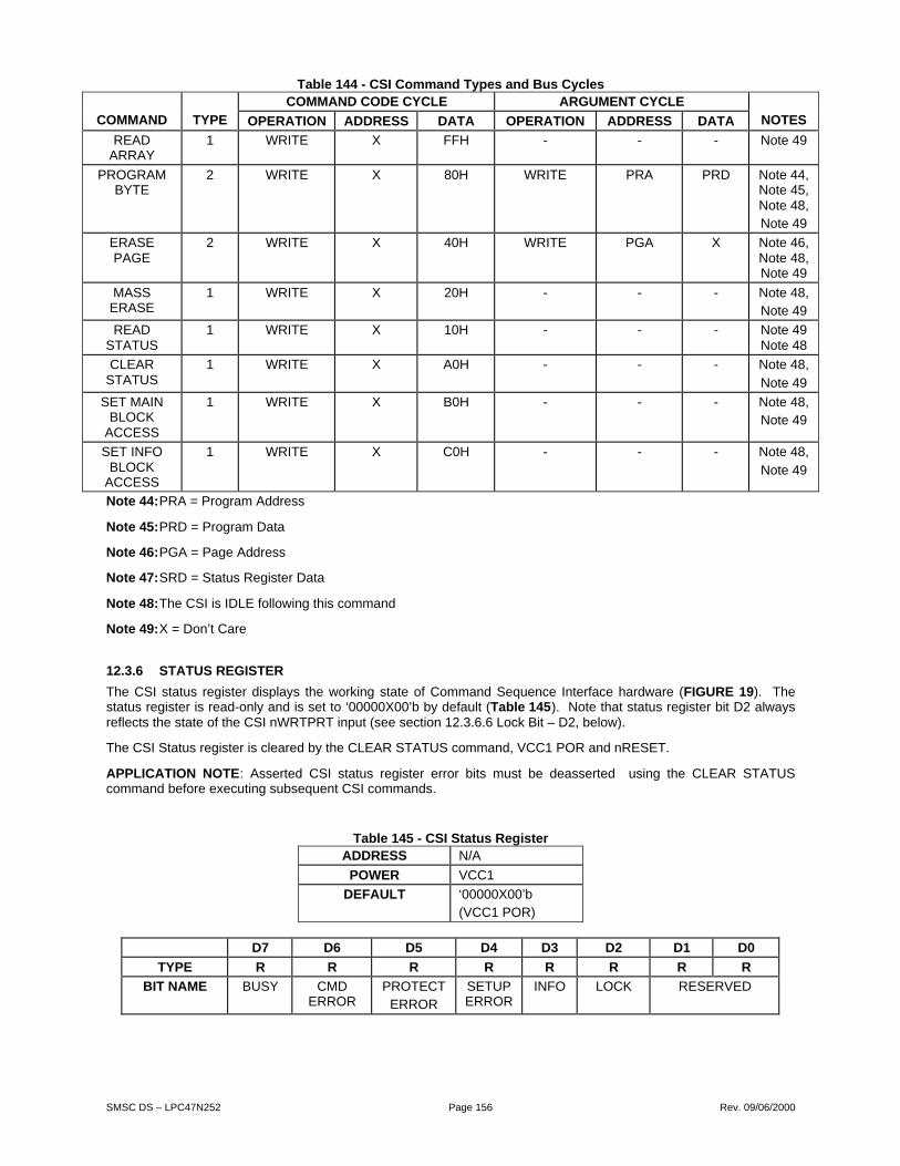
SMSC DS – LPC47N252 Page 156 Rev. 09/06/2000
Table 144 - CSI Command Types and Bus CyclesCOMMAND CODE CYCLE ARGUMENT CYCLE
COMMAND TYPE OPERATION ADDRESS DATA OPERATION ADDRESS DATA NOTES
READARRAY
1 WRITE X FFH - - - Note 49
PROGRAMBYTE
2 WRITE X 80H WRITE PRA PRD Note 44,Note 45,Note 48,Note 49
ERASEPAGE
2 WRITE X 40H WRITE PGA X Note 46,Note 48,Note 49
MASSERASE
1 WRITE X 20H - - - Note 48,Note 49
READSTATUS
1 WRITE X 10H - - - Note 49Note 48
CLEARSTATUS
1 WRITE X A0H - - - Note 48,
Note 49
SET MAINBLOCK
ACCESS
1 WRITE X B0H - - - Note 48,Note 49
SET INFOBLOCK
ACCESS
1 WRITE X C0H - - - Note 48,
Note 49
Note 44:PRA = Program Address
Note 45:PRD = Program Data
Note 46:PGA = Page Address
Note 47:SRD = Status Register Data
Note 48:The CSI is IDLE following this command
Note 49:X = Don’t Care
12.3.6 STATUS REGISTER
The CSI status register displays the working state of Command Sequence Interface hardware (FIGURE 19). Thestatus register is read-only and is set to ‘00000X00’b by default (Table 145). Note that status register bit D2 alwaysreflects the state of the CSI nWRTPRT input (see section 12.3.6.6 Lock Bit – D2, below).
The CSI Status register is cleared by the CLEAR STATUS command, VCC1 POR and nRESET.
APPLICATION NOTE: Asserted CSI status register error bits must be deasserted using the CLEAR STATUScommand before executing subsequent CSI commands.
Table 145 - CSI Status RegisterADDRESS N/A
POWER VCC1
DEFAULT ‘00000X00’b(VCC1 POR)
D7 D6 D5 D4 D3 D2 D1 D0
TYPE R R R R R R R R
BIT NAME BUSY CMDERROR
PROTECTERROR
SETUPERROR
INFO LOCK RESERVED

SMSC DS – LPC47N252 Page 157 Rev. 09/06/2000
12.3.6.1 Busy Bit – D7
The BUSY indicates the state of the PROGRAM BYTE, MASS ERASE and PAGE ERASE operations. When theBUSY bit is ‘1’, either a PROGRAM BYTE, MASS ERASE or PAGE ERASE operation is in progress. When theBUSY bit is ‘1’, writes to the CSI will assert the status register CMD Error bit (see section 12.3.6.2 CMD Error Bit –D6, below). When the BUSY bit is ‘0’, program or erase operations have completed and the CSI is ready to accept acommand. The BUSY bit is cleared by VCC1 POR.
During Byte Programming, Page Erase and Mass Erase cycles, the BUSY bit is asserted at the end of the argumentbus cycle and deasserted at the falling edge of NVSTR plus Trcv (see FIGURE 22 and Table 147 in section 12.3.7.3Program Byte Mode, FIGURE 23 and Table 148 in section 12.3.7.4 Page Erase Mode and FIGURE 24 and Table149 in section 12.3.7.5 Mass Erase Mode).
The BUSY bit is not asserted during READ ARRAY, READ STATUS, CLEAR STATUS, SET MAIN BLOCK ACCESSand SET INFO BLOCK ACCESS operations. The BUSY bit is not affected by the CLEAR STATUS command. TheBUSY bit is cleared by VCC1 POR and nRESET.
12.3.6.2 CMD Error Bit – D6
The CMD ERROR identifies that either a valid command code or a RESERVED CSI command code has beenreceived or a write to the CSI has been attempted while the BUSY bit is asserted. When the CMD ERROR bit isdeasserted ‘0’, a valid command code has been written to the CSI command register. Valid CSI command codes areshown in Table 143. When the CMD ERROR bit is asserted ‘1’, a RESERVED command code has been written tothe CSI command register or a write to the CSI has been attempted while the BUSY bit is asserted (see section12.3.7.10.1 Command Errors on page 163).
The CMD ERROR bit is deasserted by the CLEAR STATUS command, VCC1 POR, and nRESET.
12.3.6.3 Protect Error Bit – D5
The PROTECT ERROR identifies byte programming and erase operations on write-protected memory (see section12.4 Flash Write Protect on page 164). When the PROTECT ERROR bit is deasserted ‘0’, assuming the bit wascleared initially, a byte programming or erase operation has been requested for non-write-protected memory. Whenthe PROTECT ERROR bit is asserted ‘1’, a byte programming or erase operation has been requested for write-protected memory (see section 12.3.7.10.2 Write Protect Errors on page 163).
The PROTECT ERROR bit is deasserted by the CLEAR STATUS command, VCC1 POR and nRESET.
12.3.6.4 Setup Error Bit – D4
The SETUP ERROR identifies byte programming and page erase setup errors. Setup errors specifically apply toType 2 CSI commands (see section 12.3.5 CSI Command Types on page 155). When the SETUP ERROR bit isdeasserted ‘0’, assuming the bit was cleared initially, the argument cycle for a Type 2 command has been completedsuccessfully. When the SETUP ERROR bit is asserted ‘1’, a Type 2 PROGRAM BYTE or ERASE PAGE commandcode cycle has been followed by a read bus cycle instead of a write (argument) cycle. (see section 12.3.7.10.3 SetupErrors on page 163).
The SETUP ERROR bit is deasserted by the CLEAR STATUS command, VCC1 POR and nRESET.
12.3.6.5 Info Bit – D3
The INFO identifies whether the Main Memory or Information Memory is selected in the Flash Memory Array (see theSET MAIN BLOCK ACCESS and SET INFO BLOCK ACCESS CSI command codes in Table 143 and section 12.3.7CSI State Sequencing on page 158).
When Information Memory is selected, the CSI status register INFO bit is asserted ‘1’. When Main Memory isselected, the CSI status register INFO bit is deasserted ‘0’. The Main Memory is selected by default following VCC1POR and nRESET.
The INFO bit is not affected by the CLEAR STATUS command.
12.3.6.6 Lock Bit – D2
The LOCK bit D2 in the CSI status register is the inverse of the nWRTPRT input (see section 12.4 Flash WriteProtect on page 164). When the nWRTPRT input is ‘1’, i.e. the boot block is not write-protected (unlocked), the CSIstatus register LOCK bit is ‘0’. When the nWRTPRT input is ‘0’, i.e. the boot block is write-protected (locked), the CSI

SMSC DS – LPC47N252 Page 158 Rev. 09/06/2000
status register LOCK bit is ‘1’. The LOCK bit is not affected by the CLEAR STATUS command and is not affected byVCC1 POR or nRESET; i.e., there is no LOCK bit default.
12.3.7 CSI STATE SEQUENCING
12.3.7.1 Overview
CSI state sequencing implies two independent and concurrent processes: the host interface function and the flashinterface function (FIGURE 19). The CSI host interface function is illustrated in FIGURE 20. The host interfacehandles user commands for the flash interface so that, for example, a MASS ERASE operation can be executed bythe flash interface while the host interface transitions to a state that allows to the initiator to measure the operationprogress.
FIGURE 20 - CSI HOST INTERFACE STATE DIAGRAM
STANDBY
READARRAY
nRESET = 1
nRESET = 0
CMD= FFh
MASSERASE
PROGRAMBYTE
PAGEERASE
CMD = 20h
CMD= 80h CMD = 40h
CMD = 10hCLEAR
STATUS
SET MAINBLOCK
ACCESS
SET INFOBLOCK
ACCESS
CMD = C0h
CMD = B0h
CMD = A0h
IDLE(READ
STATUS)
CMD = 10h

SMSC DS – LPC47N252 Page 159 Rev. 09/06/2000
12.3.7.2 Read Array Mode
READ ARRAY mode is a pass-through mode for the CSI hardware: the address bus A[15:0] is directly connected tothe memory array address inputs and the memory array data bus is directly connected to the DOUT[7:0] data bus(FIGURE 18). In READ ARRAY mode (FIGURE 21), the DOUT pins always contain the valid contents of theselected flash memory 45 ns max after the address bus has stabilized. READ ARRAY mode is the default for theKahuna embedded flash following a CSI reset (FIGURE 20). READ ARRAY mode is used during 8051 execution.
The CSI remains in READ ARRAY mode indefinitely until nRESET is asserted or a command is given to explicitlychange modes. The Flash Memory Array signals XE, YE, and SE behave as shown in FIGURE 21 for READ cycles.The Flash Memory Array signals PROG, ERASE, MAS1 and NVSTR are always ‘0’ for READ cycles. The FlashMemory Array signal OE may be driven by an inverted version of the host read signal.
In READ ARRAY mode, write cycles to the 64k Embedded Flash Host Interface program the CSI command register.
FIGURE 21 - FLASH CORE READ ARRAY TIMING DIAGRAM
Table 146 - Flash Core Read Array Timing ValuesNAME MAX (ns) COMMENT
1 Txa 45 X address access time
2 Toa 4 OE access time
3 Tya 45 Y address access time
12.3.7.3 Program Byte Mode
In Program Byte mode the CSI host interface uses the transparent address and data latches to maintain the byteprogramming arguments from the second host bus write cycle. The CSI flash interface then cycles the appropriateprogramming controls to write the flash with the new data (FIGURE 22).
The Flash Memory Array signals XE, and YE behave as shown in FIGURE 22 for Program Byte cycles; the SE signalis always “0”. The CSI status register BUSY bit is asserted as described in section 12.3.6.1 Busy Bit – D7 on page157.
At the end of a Program Byte operation, the host interface and the flash interface idle until the next command isgiven.
Toa
Tya
Txa
IFREN
XADR
XE
YADR
YE
SE
OE
DOUT

SMSC DS – LPC47N252 Page 160 Rev. 09/06/2000
FIGURE 22 – FLASH CORE PROGRAM TIMING DIAGRAM
Table 147 - Flash Core Program Timing ValuesNAME MIN MAX UNITS COMMENT
Tnvs 5 µs PROG/ERASE to NVSTR set up time
Tnvh 5 µs NVSTR hold time
Tpgs 10 µs NVSTR to program set up time
Tpgh 20 ns program hold time
Tprog 20 40 µs program time
Tads 20 ns address/data set up time
Tadh 20 ns address/data hold time
Trcv 1 µs recovery time
Thv 25 ms cumulative HV period
TpgsTnvs
Tnvh
TpghTadsTprogTprog
Tadh
Trcv
ThvThv
IFREN
XADR
XE
YADR
YE
DIN
PROG
NVSTR
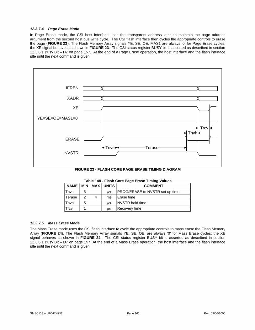
SMSC DS – LPC47N252 Page 161 Rev. 09/06/2000
12.3.7.4 Page Erase Mode
In Page Erase mode, the CSI host interface uses the transparent address latch to maintain the page addressargument from the second host bus write cycle. The CSI flash interface then cycles the appropriate controls to erasethe page (FIGURE 23). The Flash Memory Array signals YE, SE, OE, MAS1 are always ‘0’ for Page Erase cycles;the XE signal behaves as shown in FIGURE 23. The CSI status register BUSY bit is asserted as described in section12.3.6.1 Busy Bit – D7 on page 157. At the end of a Page Erase operation, the host interface and the flash interfaceidle until the next command is given.
FIGURE 23 - FLASH CORE PAGE ERASE TIMING DIAGRAM
Table 148 - Flash Core Page Erase Timing ValuesNAME MIN MAX UNITS COMMENT
Tnvs 5 µs PROG/ERASE to NVSTR set up time
Terase 2 4 ms Erase time
Tnvh 5 µs NVSTR hold time
Trcv 1 µs Recovery time
12.3.7.5 Mass Erase Mode
The Mass Erase mode uses the CSI flash interface to cycle the appropriate controls to mass erase the Flash MemoryArray (FIGURE 24). The Flash Memory Array signals YE, SE, OE, are always ‘0’ for Mass Erase cycles; the XEsignal behaves as shown in FIGURE 24. The CSI status register BUSY bit is asserted as described in section12.3.6.1 Busy Bit – D7 on page 157 At the end of a Mass Erase operation, the host interface and the flash interfaceidle until the next command is given.
TeraseTnvs
TrcvTnvh
IFREN
XADR
XE
YE=SE=OE=MAS1=0
ERASE
NVSTR

SMSC DS – LPC47N252 Page 162 Rev. 09/06/2000
FIGURE 24 – FLASH CORE MASS ERASE TIMING DIAGRAM
Table 149 - Flash Core Mass Erase Timing ValuesNAME MIN MAX UNITS COMMENT
Tnvs 5 µs PROG/ERASE to NVSTR set up time
Tnvh1 100 µs NVSTR hold time
Trcv 1 µs Recovery time
Tme 2 4 ms Mass erase time
12.3.7.6 Read Status (Idle) Mode
The Read Status Mode uses the CSI host interface to disconnect the flash memory array from the DOUT bus andmakes the CSI status register available for subsequent host read cycles (FIGURE 20). Assuming all programoperations are complete, the CSI flash interface sets the Flash Memory Array interface signals to the standby modefor the duration of the Read Status mode. The CSI host interface and the Flash Memory Array remain in the ReadStatus (Idle) mode indefinitely until the next command is given. In Read Status mode, write cycles to the 64kEmbedded Flash Host Interface program the CSI command register (not shown in FIGURE 20).
12.3.7.7 Clear Status Mode
The Clear Status Mode uses the CSI host interface to disconnect the flash memory array from the DOUT bus,deasserts the status register error bits (Table 145), and makes the CSI status register available for subsequent hostread cycles (FIGURE 20). The CSI flash interface sets the Flash Memory Array signals to the standby mode for theduration of the Clear Status mode. The CSI host interface and the Flash Memory Array interface remain in the ReadStatus (Idle) mode until the next command is given.
12.3.7.8 Set Main Block Access Mode
The Set Main Block Access mode uses the CSI host interface to disconnect the flash memory array from the DOUTbus, selects the Main Memory block in the Flash Memory Array, resets the INFO bit in the CSI status register to ‘0’(see section 12.3.6.5 Info Bit – D3 on page 157), and makes the CSI status register available for subsequent hostread cycles (FIGURE 20).
The CSI flash interface sets the Flash Memory Array interface signals to the standby mode for the duration of the SetMain Block Access mode.
TmeTnvs
TrcvTnvh1
IFREN
XADR
XE
MAS1
YE=SE=OE=0
ERASE
NVSTR

SMSC DS – LPC47N252 Page 163 Rev. 09/06/2000
The CSI host interface and the Flash Memory Array interface remain in the Read Status (Idle) mode until the nextcommand is given.
12.3.7.9 Set Info Block Access Mode
The Set Info Block Access mode uses the CSI host interface to disconnect the flash memory array from the DOUTbus, selects the Information Memory block in the Flash Memory Array, sets the INFO bit in the CSI status register to‘1’ (see section 12.3.6.5 Info Bit – D3 on page 157), and makes the CSI status register available for subsequent hostread cycles (FIGURE 20).
The CSI flash interface sets the Flash Memory Array interface signals to the standby mode for the duration of the SetInfo Block Access mode.
The CSI host interface and the Flash Memory Array interface remain in the Read Status (Idle) mode until the nextcommand is given.
12.3.7.10 CSI Host Interface Error Handling
12.3.7.10.1 Command Errors
When a write to the CSI command register has been attempted while the BUSY bit is asserted, the write data isrejected (i.e. the data in the command register is not overwritten), the state machine asserts the CMD ERROR bit inthe CSI status register, and the command in progress continues to completion.
When a RESERVED command code is written to the CSI command register when the BUSY bit is deasserted, thedata in the command register is ignored, the state machine asserts the CMD ERROR bit in the CSI status register,and the CSI host interface transitions to the IDLE state (not shown in FIGURE 20).
For information regarding RESERVED command codes see Note 42 in Table 143 and section 12.3.6.2 CMD Error Bit– D6. For information regarding the BUSY bit see 12.3.6.1 Busy Bit – D7 on page 157.
12.3.7.10.2 Write Protect Errors
When a byte programming or erase operation has been requested for write-protected memory, the command isrejected, the state machine asserts the PROTECT ERROR bit in the CSI status register and transitions to the IDLEstate (not shown in FIGURE 20).
For information regarding write-protection errors see section 12.4 Flash Write Protect on page 164 and section12.3.6.3 Protect Error Bit – D5 on page 157.
12.3.7.10.3 Setup Errors
When a PROGRAM BYTE or ERASE PAGE command code cycle has been followed by a read bus cycle instead ofa write cycle, the command is terminated, the state machine asserts the SETUP ERROR bit in the CSI status registerand transitions to the IDLE state (not shown in FIGURE 20).
For information regarding setup errors see section 12.3.5 CSI Command Types on page 155 and section 12.3.6.4Setup Error Bit – D4 on page 157.
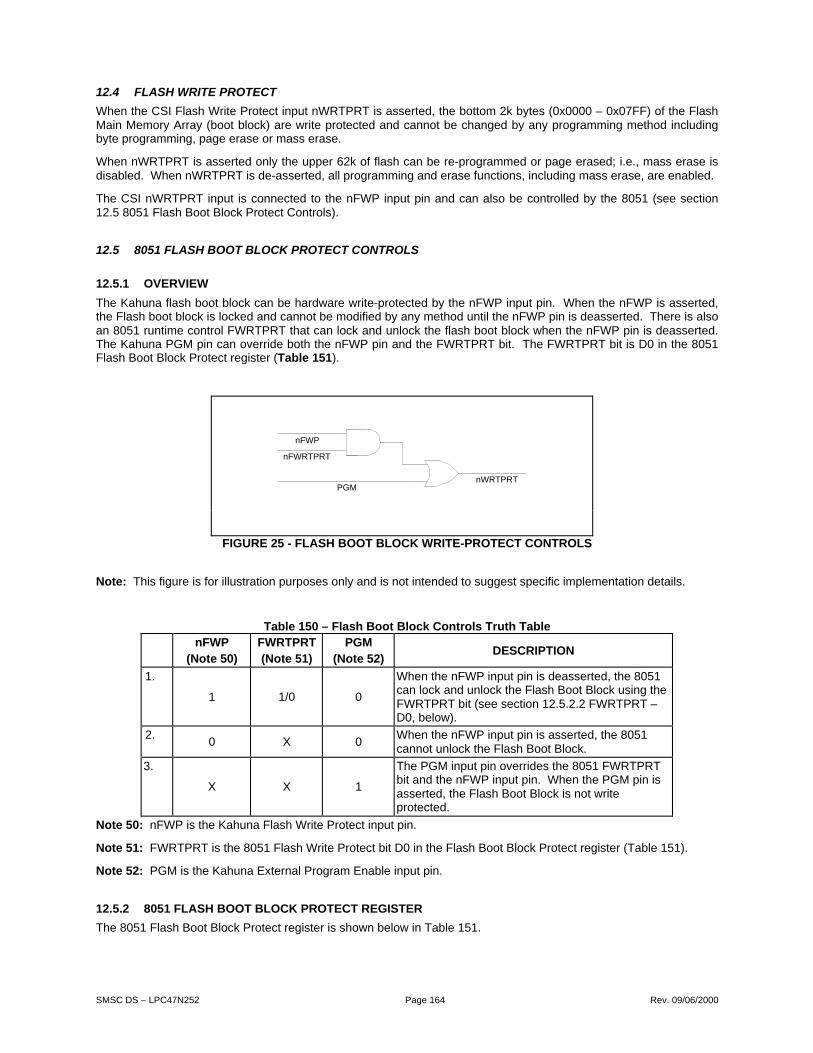
SMSC DS – LPC47N252 Page 164 Rev. 09/06/2000
12.4 FLASH WRITE PROTECT
When the CSI Flash Write Protect input nWRTPRT is asserted, the bottom 2k bytes (0x0000 – 0x07FF) of the FlashMain Memory Array (boot block) are write protected and cannot be changed by any programming method includingbyte programming, page erase or mass erase.
When nWRTPRT is asserted only the upper 62k of flash can be re-programmed or page erased; i.e., mass erase isdisabled. When nWRTPRT is de-asserted, all programming and erase functions, including mass erase, are enabled.
The CSI nWRTPRT input is connected to the nFWP input pin and can also be controlled by the 8051 (see section12.5 8051 Flash Boot Block Protect Controls).
12.5 8051 FLASH BOOT BLOCK PROTECT CONTROLS
12.5.1 OVERVIEW
The Kahuna flash boot block can be hardware write-protected by the nFWP input pin. When the nFWP is asserted,the Flash boot block is locked and cannot be modified by any method until the nFWP pin is deasserted. There is alsoan 8051 runtime control FWRTPRT that can lock and unlock the flash boot block when the nFWP pin is deasserted.The Kahuna PGM pin can override both the nFWP pin and the FWRTPRT bit. The FWRTPRT bit is D0 in the 8051Flash Boot Block Protect register (Table 151).
FIGURE 25 - FLASH BOOT BLOCK WRITE-PROTECT CONTROLS
Note: This figure is for illustration purposes only and is not intended to suggest specific implementation details.
Table 150 – Flash Boot Block Controls Truth TablenFWP
(Note 50)FWRTPRT(Note 51)
PGM(Note 52)
DESCRIPTION
1.
1 1/0 0
When the nFWP input pin is deasserted, the 8051can lock and unlock the Flash Boot Block using theFWRTPRT bit (see section 12.5.2.2 FWRTPRT –D0, below).
2. 0 X 0
When the nFWP input pin is asserted, the 8051cannot unlock the Flash Boot Block.
3.
X X 1
The PGM input pin overrides the 8051 FWRTPRTbit and the nFWP input pin. When the PGM pin isasserted, the Flash Boot Block is not writeprotected.
Note 50: nFWP is the Kahuna Flash Write Protect input pin.
Note 51: FWRTPRT is the 8051 Flash Write Protect bit D0 in the Flash Boot Block Protect register (Table 151).
Note 52: PGM is the Kahuna External Program Enable input pin.
12.5.2 8051 FLASH BOOT BLOCK PROTECT REGISTER
The 8051 Flash Boot Block Protect register is shown below in Table 151.
PGM
nFWP
nFWRTPRT
nWRTPRT

SMSC DS – LPC47N252 Page 165 Rev. 09/06/2000
Table 151 – 8051 Flash Boot Block Protect RegisterHOST ADDRESS N/A
8051 ADDRESS 0x7F88
POWER VCC1
DEFAULT 0x00
D7 D6 D5 D4 D3 D2 D1 D0
HOST TYPE - - - - - - - -
8051 TYPE R R R R R R R R/W
BIT NAME RESERVED FWRTPRT
12.5.2.1 RESERVED – D[7:1]
Bits D7 – D1 are RESERVED. RESERVED bits cannot be written and return ‘0’ when read.
12.5.2.2 FWRTPRT – D0
The Flash Write Protect bit FWRTPRT permits the 8051 to lock the Flash boot block when the nFWP input pin isdeasserted (see item #1 in Table 150). When FWRTPRT is ‘1’, the Flash Boot Block is locked, regardless of thestate of the nFWP input pin. When FWRTPRT is ‘0’ (default), the Flash Boot Block is unlocked if the nFWP pin isdeasserted.
12.6 FLASH CSI PROGRAMMING EXAMPLES
12.6.1 OVERVIEW
This section provides two C-like examples of Kahuna 64k Embedded Flash programming using the CSI ProgramByte and Mass Erase commands. As shown in the examples that follow, all transactions with the Kahuna 64kEmbedded Flash CSI Host Interface are simple read and write functions.
There is also another function NO_ERRORS_&_BUSY described here that is used in both the Program Byte andMass Erase examples to check the CSI Status register during programming operations.
For the purposes of these examples all functions use the 8051 Flash Programming Interface (see section 13.4 8051Flash Program Access on page 171). It is also assumed that the 64k Embedded Flash ROM Main Memory Block isselected and that the Flash is in the Read Array mode before the examples begin.
12.6.1.1 CSIWRITE Function
The CSIWRITE function uses the 8051 Program Access registers to write to the CSI Host interface (FIGURE 26).For information regarding how to activate the 8051 Program Access Interface see section 13.2 Flash ProgramInterface Decoder.
The CSIWRITE function requires two parameters ‘address’ and ‘data’, although the address argument is not relevantduring CSI Command Code cycles. Note that the address register arguments are initialized before the data registertransaction occurs.

SMSC DS – LPC47N252 Page 166 Rev. 09/06/2000
// DeclarationsHIGH_ADDR_REG = 0x7FB0; // 16-bit High Addr. register MMCR Address.LOW_ADDR_REG = 0x7FB1; // 16-bit Low Addr. register MMCR Address.DATA_REG = 0x7FB2; // 16-bit Data register MMCR Address.
// Executable Codevoid CSIWRITE(int address, int data) { // Load Address Registers First. outportb(HIGH_ADDR_REG, // Load High Address Register. ((address >> 8) & 0xFF)); outportb(LOW_ADDR_REG, (address & 0xFF)); // Load Low Address Register. outportb(DATA_REG, (data & 0xff)); // Write Data Register Last. };
FIGURE 26 - CSIWRITE COMMAND FUNCTION
12.6.1.2 CSIREAD Function
The CSIREAD function uses the 8051 Program Access registers to read to the CSI Host interface (FIGURE 24). Forinformation regarding how to activate the 8051 Program Access Interface, see section 13.2 Flash Program InterfaceDecoder.
The CSIREAD function requires one parameter ‘address’ and returns the read data value. Note that the addressparameter is not relevant during CSI Status Register read cycles.
// DeclarationsHIGH_ADDR_REG = 0x7FB0; // 16-bit High Addr. register MMCR Address.LOW_ADDR_REG = 0x7FB1; // 16-bit Low Addr. register MMCR Address.DATA_REG = 0x7FB2; // 16-bit Data register MMCR Address.
// Executable Codeint CSIREAD(int address) { // Load Address Registers First. outportb(HIGH_ADDR_REG, // Load High Address Register. ((address >> 8) & 0xFF)); outportb(LOW_ADDR_REG, (address & 0xFF)); // Load Low Address Register. return (inportb(DATA_REG)); // Read and Return Data Register Value. };
FIGURE 27 - CSIREAD COMMAND FUNCTION
12.6.1.3 NO_ERRORS_&_BUSY Function
The NO_ERRORS_&_BUSY function (FIGURE 28) is used in a ‘while’ loop in FIGURE 29 and FIGURE 30 to checkthe CSI status register during byte program and page erase operations.
Note: The NO_ERRORS_&_BUSY function can only be used when the CSI Host interface is in the Read Status(Idle) state (see section 12.3.7.6 Read Status (Idle) Mode on page 162).
The NO_ERRORS_&_BUSY function requires one parameter ‘errors’ and returns TRUE when there are no errorsand the BUSY bit is asserted or FALSE when errors have occurred or the BUSY bit is deasserted. The ‘errors’parameter is an integer pointer for the CSI Status register error flags.

SMSC DS – LPC47N252 Page 167 Rev. 09/06/2000
// DeclarationsERROR_MASK = 0x0070; // CSI Status Reg. Error Bits Mask.BUSY_MASK = 0x0080; // CSI Status Reg. Busy Bit Mask.
// Executable Codeboolean NO_ERRORS_&_BUSY (int *errors) // NOTE: Call only in CSI Idle (Read Status) State. { int etmp; // Temp Value for CSI Status Register. etmp = CSIREAD(0x0000); // Get CSI Status Register (Address = Don’t Care). IF (*errors = (etmp & ERROR_MASK)) // First Check for Errors. return (FALSE); // Stop Loop Because of Error Flags. ELSE IF (etmp & BUSY_MASK) // Look at Busy Bit. return (TRUE); // Continue Loop Because Busy Bit Asserted. ELSE return (FALSE); // Stop Loop Because Busy Bit Deasserted and No Errors. };
FIGURE 28 - NO_ERRORS_&_BUSY FUNCTION
12.6.2 BYTE PROGRAMMING EXAMPLE
Byte programming requires three basic steps: 1) activate the CSI Host Interface with the Program Byte commandcode, 2) send the program address and data arguments to the CSI address & data latches, and 3) monitor thecompletion status and check for errors.
The byte programming example pseudo-code is shown below in FIGURE 29. A return to the Read Array mode isalso shown in FIGURE 29 to verify the Program Byte operation.
// DeclarationsDONE = FALSE; // Programming Loop Control VariableWRITE_ADDRESS = 00F0; // Program Byte Address Argument ValueWRITE_DATA = 0xA0; // Program Byte Data Argument ValuePROGRAM_BYTE_CMD = 0x80; // CSI Program Byte Command Code ValueREAD_ARRAY_CMD = 0xFF; // CSI Read Array Command Code ValueCLEAR_STATUS_CMD = 0xA0; // CSI Clear Status Command Code ValueERRORS = 0x00; // Variable for Status Register Errors
// Executable CodeWHILE (NOT DONE) { CSIWRITE(0x0000, PROGRAM_BYTE_CMD); // Send Program Byte Command Code (Address = Don’t Care). CSIWRITE(WRITE_ADDRESS, WRITE_DATA); // Send Program Byte Argument. WHILE (NO_ERRORS_&_BUSY(&ERRORS)); // Loop Until Errors Occur or BUSY Bit Deasserted. IF (ERRORS) // Take Remedial Steps. { FIX_ERRORS(ERRORS); // Correct Problems (e.g. Protect or Setup Errors). CSIWRITE(0x0000, CLEAR_STATUS_CMD); // Clear Status Register (Address = Don’t Care). } // Try Again. ELSE // Restore Read Array Mode To Verify Byte Programming. { CSIWRITE(0x0000, READ_ARRAY_CMD); IF (CSIREAD(WRITE_ADDRESS) = WRITE_DATA) // If Not Verified, Try Again. DONE = TRUE; } }
FIGURE 29 - PROGRAM BYTE EXAMPLE PSEUDO-CODE

SMSC DS – LPC47N252 Page 168 Rev. 09/06/2000
12.6.3 MASS ERASE EXAMPLE
Mass Erase requires two basic steps: 1) activate the CSI Host Interface with the Mass Erase command code and 2)monitor the completion status and check for errors. The Mass Erase example pseudo-code is shown in FIGURE 30.A return to the Read Array mode is also shown in FIGURE 30.
// DeclarationsDONE = FALSE; // Programming Loop Control VariableMASS_ERASE_CMD = 0x20; // CSI Mass Erase Command Code ValueREAD_ARRAY_CMD = 0xFF; // CSI Read Array Command Code ValueCLEAR_STATUS_CMD = 0xA0; // CSI Clear Status Command Code ValueERRORS = 0x00; // Variable for Status Register Errors
// Executable CodeWHILE (NOT DONE) { CSIWRITE(0x0000, MASS_ERASE_CMD); // Send Mass Erase Command Code (Address = Don’t Care). // No Argument Cycle Required. WHILE (NO_ERRORS_&_BUSY(&ERRORS)); // Loop Until Errors Occur or BUSY Bit Deasserted. IF (ERRORS) // Take Remedial Steps { FIX_ERRORS(ERRORS); // Correct Problems (e.g. Protect Error). CSIWRITE(0x0000, CLEAR_STATUS_CMD); // Clear Status Register (Address = Don’t Care). } // Try Again. ELSE // Restore Read Array Mode { CSIWRITE(0x0000, READ_ARRAY_CMD); // Address = Don’t Care. DONE = TRUE; } }
FIGURE 30 - MASS ERASE EXAMPLE PSEUDO-CODE
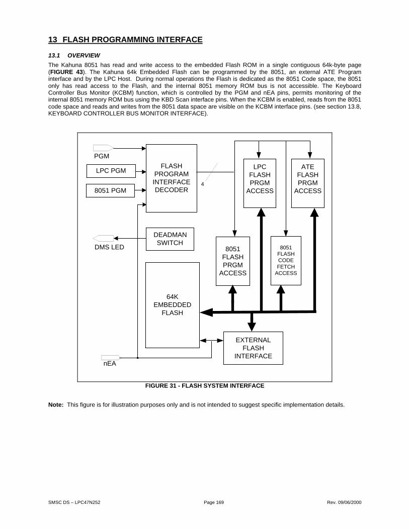
SMSC DS – LPC47N252 Page 169 Rev. 09/06/2000
13 FLASH PROGRAMMING INTERFACE
13.1 OVERVIEW
The Kahuna 8051 has read and write access to the embedded Flash ROM in a single contiguous 64k-byte page(FIGURE 43). The Kahuna 64k Embedded Flash can be programmed by the 8051, an external ATE Programinterface and by the LPC Host. During normal operations the Flash is dedicated as the 8051 Code space, the 8051only has read access to the Flash, and the internal 8051 memory ROM bus is not accessible. The KeyboardController Bus Monitor (KCBM) function, which is controlled by the PGM and nEA pins, permits monitoring of theinternal 8051 memory ROM bus using the KBD Scan interface pins. When the KCBM is enabled, reads from the 8051code space and reads and writes from the 8051 data space are visible on the KCBM interface pins. (see section 13.8,KEYBOARD CONTROLLER BUS MONITOR INTERFACE).
FIGURE 31 - FLASH SYSTEM INTERFACE
Note: This figure is for illustration purposes only and is not intended to suggest specific implementation details.
EXTERNALFLASH
INTERFACE
64KEMBEDDED
FLASH
PGM
DMS LED
FLASHPROGRAMINTERFACEDECODER
LPC PGM
8051 PGM
DEADMANSWITCH
LPCFLASHPRGM
ACCESS
ATEFLASHPRGM
ACCESS
8051FLASHCODEFETCH
ACCESS
8051FLASHPRGM
ACCESS
4
nEA

SMSC DS – LPC47N252 Page 170 Rev. 09/06/2000
13.2 FLASH PROGRAM INTERFACE DECODER
The Flash Program Interface Decoder controls access to the Kahuna 64k Embedded Flash.
The Flash configurations described below depend upon the state of the PGM and nEA pins and the LPC PGM and8051 PGM bits in the Flash Program register. The ATE PGM and EXT FLASH bits in the Flash Program registerreflect the state of the the PGM and nEA pins. When the PGM and nEA pins are asserted, the Flash ProgramInterface Decoder enters the KCBM Interface state (see Table 152, items# 6, 7 and 8). The PGM and nEA pinscontrol both the function enable and the pin multiplexing for the KCBM Interface. Table 152 below provides the truthtable for the Flash Program Interface Decoder. See section 13.10 for a description of the Flash Program register.
Table 152 - Flash Program Interface Decoder Truth TableFLASH PROGRAM REGISTER
EXT
FLASH (D3)(Note 1)
ATE PGM
(D2)(Note 2)
LPCPGM(D1)
8051PGM(D0)
MODE DESCRIPTION
1. 0 0 0 0 8051CODEFETCHACCESS
The Flash is dedicated as the 8051Code space. The 8051 only has readaccess to the Flash in this mode.
2. 0 0 1 0 LPCPROGRAMACCESS
The Flash is dedicated to the LPC Hostprogramming interface.
3. 0 0 X 1 8051PROGRAMACCESS
The Flash is dedicated to the 8051programming interface. When thismode is selected, the LPC Hostprogramming interface cannot beenabled; i.e., the LPC PGM bit isirrelevant. The 8051 must only executeprogram code from the 256-byteInternal Scratch ROM.
4. 0 1 0 0 ATEPROGRAMACCESS
The Flash is dedicated to the ATEprogramming interface. When thismode is selected, both the LPC Hostprogramming interface and the 8051programming interface are disabled;i.e., the LPC PGM and the 8051 PGMbits are reset to ‘0’
5. 1 0 X X EXTERNALFLASH
The 8051 is running out of externalFlash. When this mode is selected, theATE, LPC Host and 8051 programminginterfaces cannot be enabled
6. 1 1 0 0 KCBM -8051CODEFETCHACCESS
The KCBM function is enabled and theFlash is dedicated as the 8051 Codespace. The 8051 only has read accessto the Flash in this mode. The KCBMinterface monitors activity on theinternal 8051 ROM bus.
7. 1 1 X 1 KCBM -8051PROGRAMACCESS
The KCBM function is enabled and theFlash is dedicated to the 8051programming interface. The 8051executes program code from the 256-byte Internal Scratch ROM. The KCBMinterface monitors access to theInternal Scratch ROM (8051 ROM bus).

SMSC DS – LPC47N252 Page 171 Rev. 09/06/2000
FLASH PROGRAM REGISTER
EXT
FLASH (D3)(Note 1)
ATE PGM
(D2)(Note 2)
LPCPGM(D1)
8051PGM(D0)
MODE DESCRIPTION
8. 1 1 1 0 KCBM -LPCPROGRAMACCESS
The KCBM function is enabled and thethe Flash is dedicated to the LPCprogramming interface. The 8051 isheld in reset during all LPC FlashProgram Access operations. The stateof the KCBM interface is undefined inthis mode.
Note 1: the EXT FLASH bit D3 in the Flash Program register is the inverse of the nEA pin.Note 2: the ATE PGM bit D2 in the Flash Program register is the PGM pin.
13.3 8051 CODE FETCH ACCESS
The 8051 Code Fetch Access function uses the 64k Embedded Flash as the 8051 program memory space (FIGURE32). The 8051 Code Fetch Access function is enabled when bits D3 – D0 in the Flash Program register are ‘0’ (seeTable 152 and section 13.10 Flash Program Register).
Note: When the 8051 Code Fetch Access function is selected and the MMC bit is ‘1’, the 8051 can execute from the64k Embedded Flash and from the Internal Scratch ROM (see section 13.11 Internal Scratch ROM on page 183).
8051
mem_addr[15:0]
mem_data_in
mem_psrd_n
64KEMBEDDED
FLASH
A[15:0]
DOUT[7:0]
nRD
FIGURE 32 - 8051 CODE FETCH ACCESS INTERFACENote: This figure is for illustration purposes only and is not intended to suggest specific implementation details.
13.4 8051 FLASH PROGRAM ACCESS
The 8051 Flash Program Access function enables the 64k Embedded Flash to be programmed from an internalparallel hardware interface using 8051 memory-mapped control registers (see section 13.11 8051/LPC FlashProgram Access Registers on page 183 and FIGURE 33). The 8051 PGM bit D0 in the Flash Program register isused to enable the 8051 Program Access function (see section 13.10.6 8051 PGM – D0).
APPLICATION NOTE: The 8051 must only execute program code from the 256-byte Internal Scratch ROM to usethe 8051 Flash Program Access function (see section 13.11 Internal Scratch ROM on page 183). When Flashprogramming operations are completed, the 8051 must return the Embedded Flash to the READ ARRAY state (Table143) before returning to the 8051 Code Fetch Access mode (Table 152). The 8051 must return the Embedded Flashto Read-Array mode when programming has been completed before jumping out of the Internal Scratch ROM codespace.
To program the 64k Embedded Flash using the 8051 Flash Program Access function, first use the HIGH ADDRESS(0x7FB0) and LOW ADDRESS (0x7FB1) registers for program and page address arguments and then the DATAregister (0x7FB2) for program data, read data, command codes and status data.
Note: Address arguments for Program Byte and Page Erase operations must be initialized in the 8051 FlashProgram Access address registers before read and write commands to the CSI Host Interface are activated by readsand writes to the 8051 Flash Program Access DATA register (0x7FB2).

SMSC DS – LPC47N252 Page 172 Rev. 09/06/2000
For information regarding the programming sequence for the Kahuna 64k Embedded Flash see section 12.3Command Sequence Interface starting on page 153.
64KEMBEDDED
FLASH
LOWADDRESS(MBX80h)(0x7FB1)
TRISTATEDRIVER
A[15:8]
A[7:0]
DOUT[7:0]
DIN[7:0]
nRD
nWE
HIGHADDRESS(MBX9Fh)(0x7FB0)
DATA(MBX81h)(0x7FB2)
FIGURE 33 – 8051/LPC FLASH PROGRAM ACCESSNote: This figure is for illustration purposes only and is not intended to suggest specific implementation details.
13.5 LPC BUS FLASH PROGRAM ACCESS
The LPC Flash Program Access function enables the 64k Embedded Flash to be programmed from an internalparallel hardware interface (see FIGURE 33 above.) The LPC Flash Program Access function uses the registers inthe Mailbox Registers Interface (see section 13.11 8051/LPC Flash Program Access Registers on page 183). TheLPC PGM bit D1 in the Flash Program register is used to enable the LPC Program Access function (see section13.10.5 LPC PGM – D1, below). The LPC Flash Program Access function can only be enabled when the ATE PGMand the 8051 PGM bits are deasserted ‘0’ (Table 152), and the SYSTEM FLASH bit in the Disable register isdeasserted ‘0’(See Section 11.8.3.1, Disable Register on page 132.)
APPLICATION NOTE: The 8051 must be stopped to use the LPC Bus Flash Program Access function. When Flashprogramming operations are completed, the LPC Host must return the Embedded Flash to the READ ARRAY state(Table 143) before returning to the 8051 Code Fetch Access mode (Table 152) and restarting the 8051 clock.
To program the 64k Embedded Flash using the LPC Bus Flash Program Access function, first use the Flash HighAddress (MBX9Fh) and Flash Low Address (MBX80h) registers for program and page address arguments and thenthe Flash Data register (MBX81h) for program data, read data, command codes and status data.
Note: Address arguments for Program Byte and Page Erase operations must be initialized in the LPC FlashProgram Access address registers before read and write commands to the CSI Host Interface are activated by readsand writes to the LPC Flash Program Access DATA register (MBX81h).
For information regarding the programming sequence for the Kahuna 64k Embedded Flash see section 12.3Command Sequence Interface starting on page 153.
13.6 ATE FLASH PROGRAM ACCESS
13.6.1 OVERVIEW
The ATE Flash Program Access function enables the 64k Embedded Flash to be programmed from an externalparallel hardware interface using the KBD Scan interface in the Kahuna pin configuration. The Flash ProgramInterface Decoder enables the ATE Flash Program Access function (Table 152, item #4).
A block diagram of the ATE Flash Program Access Interface is shown below in FIGURE 34. The ATE Flash ProgramAccess pin mapping to the KBD Scan interface pins is shown in Table 153. For information regarding theprogramming sequence for the Kahuna 64k Embedded Flash see section 12.3 Command Sequence Interfacestarting on page 153.

SMSC DS – LPC47N252 Page 173 Rev. 09/06/2000
64KEMBEDDED
FLASH
FPA[15:8]
LATCH
TRISTATEDRIVER
FPAD[7:0]
nFPRD
FPALE
nFPWR
A[15:8]
A[7:0]
DOUT[7:0]
DIN[7:0]
nRD
nWE
FIGURE 34 - ATE FLASH PROGRAM ACCESS INTERFACENote: This figure is for illustration purposes only and is not intended to suggest specific implementation details.
Table 153 - ATE Flash Program Access Interface KBD Scan Pin Mapping
KBD SCANINTERFACE
PINS
ATE FLASH
PROGACCESS
INTERFACE DESCRIPTION
1. KSO0 FPA15
2. KSO1 FPA14
3. KSO2 FPA13
4. KSO3 FPA12
5. KSO4 FPA11
6. KSO5 FPA10
7. KSO6 FPA9
8. KSO7 FPA8
High-Order Address Bus A15 – A8.
9. KSO8 FPAD7
10. KSO9 FPAD6
11. KSO10 FPAD5
12. KSO11 FPAD4
13. KSI0 FPAD3
14. KSI1 FPAD2
15. KSI2 FPAD1
16. KSI3 FPAD0
Multiplexed Low-Order Address Bus A7 –A0 and Data Bus D0 – D7. The Low-OrderAddress Bus is Latched with FPALE.
17. KSI4 FPALE Low-Order Address Bus Latch Control
18. KSI5 nFPRD Active-Low ATE Flash Program AccessInterface READ Signal.
19. KSI6 nFPWR Active-Low ATE Flash Program AccessInterface WRITE Signal.
Note: All ATE Flash Program Access Interface signals in Table 153 refer to FIGURE 34.
All KDB SCAN Interface pins refer to the Kahuna pin configuration.

SMSC DS – LPC47N252 Page 174 Rev. 09/06/2000
13.6.2 ATE FLASH PROGRAM TIMING
t2t1
t5 t6
t3
t4t7
t10DATA
FPA[7:0] FPA[7:0]
FPA[15:8] FPA[15:8]
FPALE
nFPRDnFPWR
FPAD[7:0]
FPA[15:8]
t9
t8
FIGURE 35 – ATE FLASH PROGRAM ACCESS INTERFACE TIMING
Table 154 - ATE Flash Program Access Interface Write Timing Parameters
PARAMETER MIN TYP MAX UNITS
OURTEST
VALUE
t1 FPALE Pulse Width TBD 50 ns 50ns
t2 Address Valid to FPALE Low TBD 50 ns 50ns
t4 FPALE Low to Valid data In 10 TBD ns 10 ns
t5 FPALE Low to nFPWR Low TBD 5 ns 5 ns
t6 nFPWR Pulse Width TBD 50 ns 50 us
t7 nFPWR Low to Valid Data In TBD 5 ns 5 ns
t8 Valid data Hold Time FollowingnFPWR Low-To-High Transition
TBD 10 ns 10 ns
t9 nFPWR High to FPALE High TBD 0 ns 0 ns
Table 155 - ATE Flash Program Access Interface Read Timing Parameters
PARAMETER MIN TYP MAX UNITS
t1 FPALE Pulse Width TBD 50 ns
t2 Address Valid to FPALE Low TBD 50 ns
t3 nFPRD Low to Address Float 0 ns
t4 FPALE Low to Valid data Out 10 TBD ns
t5 FPALE Low to nFPRD Low TBD 5 ns
t6 nFPRD Pulse Width TBD 50 ns
t7 nFPRD Low to Valid Data Out TBD 5 ns
t8 Valid data Hold Time FollowingnFPRD Low-To-High Transition
TBD 10 ns
t9 nFPRD High to FPALE High 0
t10 Data Float Following nFPRD Low-To-High Transition
0 ns
Note: The values in Table 154 and Table 155 come from SMSC ATE testing and shall be updated whencharacterization is complete.

SMSC DS – LPC47N252 Page 175 Rev. 09/06/2000
1 2 3 4 5 6test vector
FPA15:8
FPAD7:0
FPALE
nFPRD
nFPWR
PGM
valid addr
valid addr
ALE latches validaddress
issue a CSIprogam command
provide data to beprogrammed into
flashwiat 48 us
issue a CSI readcommand
read by valid dataform flash
00h valid data
valid data80h
00h
FFh
valid data
valid data
Ù Test cycle time is 60ns.Ù Pulse width of FPALE, nFPRD, and nPFWR is 50ns.Ù The wait in vector 4 is 1200x 60ns=48us
FIGURE 36 – KAHUNA ATE FLASH PROGRAM INTERFACE TIMING
APPLICATION NOTE: An effort should be made to prevent software from asserting the nRESET input while theBUSY bit is asserted to avoid programming errors or incomplete erase cycles (see section 12.3.6 Status Register onpage 156).
13.6.3 PGM PIN
The PGM pin enables the ATE Flash Program access function. When the PGM pin is the exclusively asserted inputto the Flash Program Interface Decoder (Table 152, item #4) the 64k Embedded Flash interface is directly connectedto the ATE Flash Program Access interface, the KBD Scan interface pin multiplexing is configured to support ATEFlash Program Access, the 8051 is stopped (reset), and all Flash write-protect functions are disabled (see section12.5 8051 Flash Boot Block Protect Controls on page 164).
To stop the 8051, when the PGM pin is asserted (‘1’) the rst_in_n input to the 8051 is asserted (‘0’). When the PGMpin is de-asserted, the 64k Embedded Flash interface is re-connected to the 8051, the Embedded Flash is reset toREAD ARRAY mode, the rst_in_n input to the 8051 is deasserted and the Flash write-protect function is re-enabled.
13.7 EXTERNAL FLASH INTERFACE
The External Flash Interface function enables the 8051 program memory to reside in an external ROM device usingthe KBD Scan Interface in the Kahuna pin configuration. A block diagram of the External Flash Interface is shownbelow in FIGURE 37. The External Flash Interface pin mapping to the KBD Scan interface pins is shown in Table156. The Flash Program Interface Decoder enables the the External Flash Interface function (Table 152, item #5).When the nEA pin is asserted the 8051 program memory is disconnected from 64k Embedded Flash interface andconnected to the External Flash Interface, the KBD Scan interface pin multiplexing is configured to support theExternal Flash Interface, and the 64k Embedded Flash is placed in a Reset state (see section 0 on page 154.)
Note: The Kahuna External Flash Interface only supports 8051 ROM read cycles (FIGURE 38 and Table 157). TheExternal Flash Interface is compatible with flash devices like the Intel 28F004.

SMSC DS – LPC47N252 Page 176 Rev. 09/06/2000
8051
mem_addr[15:8]
mem_data_in
mem_addr[7:0]
EFA[15:8]
mem_psrd_n
EFAD[7:0]
nEFRD
mem_aleEFALE
FIGURE 37 - KAHUNA EXTERNAL FLASH INTERFACENote: This figure is for illustration purposes only and is not intended to suggest specific implementation details.
Table 156 – External Flash Interface KBD Scan Pin Mapping
KBD SCANPINS
EXTERNALFLASH
INTERFACE DESCRIPTION
1. KSO0 EFA15
2. KSO1 EFA14
3. KSO2 EFA13
4. KSO3 EFA12
5. KSO4 EFA11
6. KSO5 EFA10
7. KSO6 EFA9
8. KSO7 EFA8
High-Order Address Bus A15 – A8.
9. KSO8 EFAD7
10. KSO9 EFAD6
11. KSO10 EFAD5
12. KSO11 EFAD4
13. KSI0 EFAD3
14. KSI1 EFAD2
15. KSI2 EFAD1
16. KSI3 EFAD0
Multiplexed Low-Order Address Bus A7 -A0 and Data Bus D0 – D7. The Low-Order Address Bus is Latched Externallywith EFALE.
17. KSI4 EFALE Low-Order Address Bus Latch Control
18. KSI5 nEFRD Active-Low External Flash InterfaceREAD Signal.
Note: All External Flash Interface signals in Table 156 refer to FIGURE 37. All KDB SCAN Interface pins refer to theKahuna pin configuration.
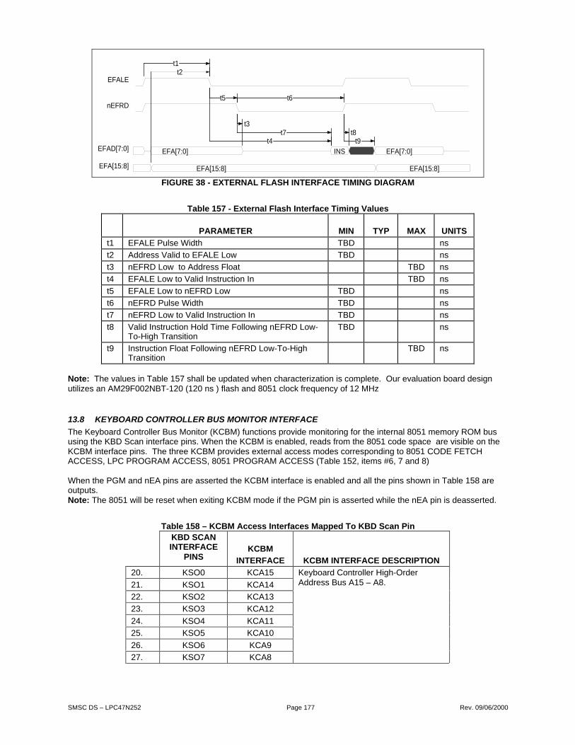
SMSC DS – LPC47N252 Page 177 Rev. 09/06/2000
t2t1
t5 t6
t3
t4t7 t8
t9
INSEFA[7:0] EFA[7:0]
EFA[15:8] EFA[15:8]
EFALE
nEFRD
EFAD[7:0]
EFA[15:8]
FIGURE 38 - EXTERNAL FLASH INTERFACE TIMING DIAGRAM
Table 157 - External Flash Interface Timing Values
PARAMETER MIN TYP MAX UNITS
t1 EFALE Pulse Width TBD ns
t2 Address Valid to EFALE Low TBD ns
t3 nEFRD Low to Address Float TBD ns
t4 EFALE Low to Valid Instruction In TBD ns
t5 EFALE Low to nEFRD Low TBD ns
t6 nEFRD Pulse Width TBD ns
t7 nEFRD Low to Valid Instruction In TBD ns
t8 Valid Instruction Hold Time Following nEFRD Low-To-High Transition
TBD ns
t9 Instruction Float Following nEFRD Low-To-HighTransition
TBD ns
Note: The values in Table 157 shall be updated when characterization is complete. Our evaluation board designutilizes an AM29F002NBT-120 (120 ns ) flash and 8051 clock frequency of 12 MHz
13.8 KEYBOARD CONTROLLER BUS MONITOR INTERFACE
The Keyboard Controller Bus Monitor (KCBM) functions provide monitoring for the internal 8051 memory ROM bususing the KBD Scan interface pins. When the KCBM is enabled, reads from the 8051 code space are visible on theKCBM interface pins. The three KCBM provides external access modes corresponding to 8051 CODE FETCHACCESS, LPC PROGRAM ACCESS, 8051 PROGRAM ACCESS (Table 152, items #6, 7 and 8)
When the PGM and nEA pins are asserted the KCBM interface is enabled and all the pins shown in Table 158 areoutputs.Note: The 8051 will be reset when exiting KCBM mode if the PGM pin is asserted while the nEA pin is deasserted.
Table 158 – KCBM Access Interfaces Mapped To KBD Scan PinKBD SCANINTERFACE
PINSKCBM
INTERFACE KCBM INTERFACE DESCRIPTION
20. KSO0 KCA15
21. KSO1 KCA14
22. KSO2 KCA13
23. KSO3 KCA12
24. KSO4 KCA11
25. KSO5 KCA10
26. KSO6 KCA9
27. KSO7 KCA8
Keyboard Controller High-OrderAddress Bus A15 – A8.
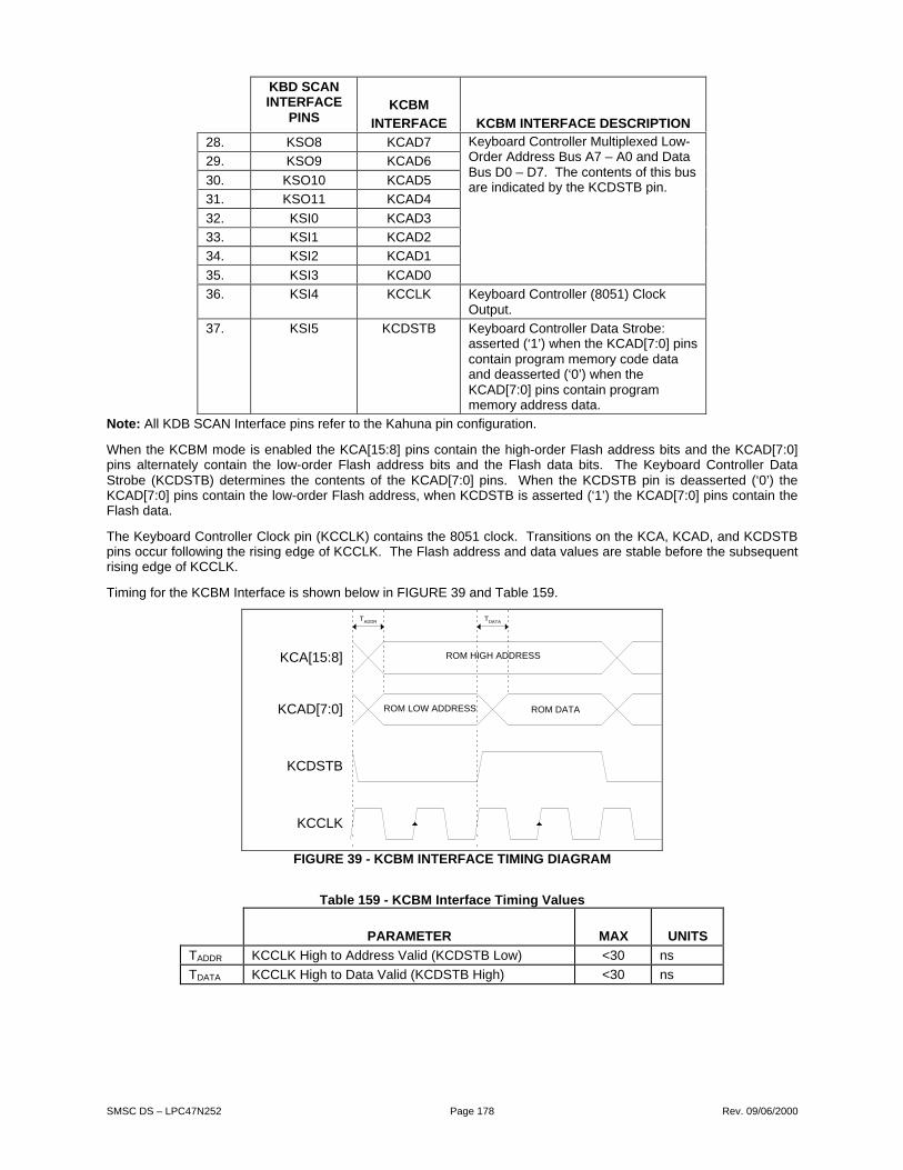
SMSC DS – LPC47N252 Page 178 Rev. 09/06/2000
KBD SCANINTERFACE
PINSKCBM
INTERFACE KCBM INTERFACE DESCRIPTION
28. KSO8 KCAD7
29. KSO9 KCAD6
30. KSO10 KCAD5
31. KSO11 KCAD4
32. KSI0 KCAD3
33. KSI1 KCAD2
34. KSI2 KCAD1
35. KSI3 KCAD0
Keyboard Controller Multiplexed Low-Order Address Bus A7 – A0 and DataBus D0 – D7. The contents of this busare indicated by the KCDSTB pin.
36. KSI4 KCCLK Keyboard Controller (8051) ClockOutput.
37. KSI5 KCDSTB Keyboard Controller Data Strobe:asserted (‘1’) when the KCAD[7:0] pinscontain program memory code dataand deasserted (‘0’) when theKCAD[7:0] pins contain programmemory address data.
Note: All KDB SCAN Interface pins refer to the Kahuna pin configuration.
When the KCBM mode is enabled the KCA[15:8] pins contain the high-order Flash address bits and the KCAD[7:0]pins alternately contain the low-order Flash address bits and the Flash data bits. The Keyboard Controller DataStrobe (KCDSTB) determines the contents of the KCAD[7:0] pins. When the KCDSTB pin is deasserted (‘0’) theKCAD[7:0] pins contain the low-order Flash address, when KCDSTB is asserted (‘1’) the KCAD[7:0] pins contain theFlash data.
The Keyboard Controller Clock pin (KCCLK) contains the 8051 clock. Transitions on the KCA, KCAD, and KCDSTBpins occur following the rising edge of KCCLK. The Flash address and data values are stable before the subsequentrising edge of KCCLK.
Timing for the KCBM Interface is shown below in FIGURE 39 and Table 159.
ROM HIGH ADDRESS
ROM LOW ADDRESS ROM DATA
TADDR TDATA
KCA[15:8]
KCAD[7:0]
KCDSTB
KCCLK
FIGURE 39 - KCBM INTERFACE TIMING DIAGRAM
Table 159 - KCBM Interface Timing Values
PARAMETER MAX UNITS
TADDR KCCLK High to Address Valid (KCDSTB Low) <30 ns
TDATA KCCLK High to Data Valid (KCDSTB High) <30 ns
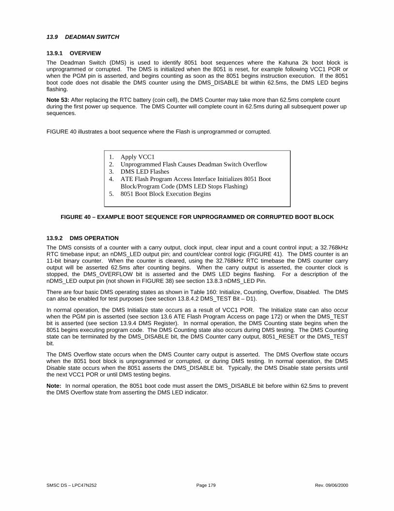
SMSC DS – LPC47N252 Page 179 Rev. 09/06/2000
13.9 DEADMAN SWITCH
13.9.1 OVERVIEW
The Deadman Switch (DMS) is used to identify 8051 boot sequences where the Kahuna 2k boot block isunprogrammed or corrupted. The DMS is initialized when the 8051 is reset, for example following VCC1 POR orwhen the PGM pin is asserted, and begins counting as soon as the 8051 begins instruction execution. If the 8051boot code does not disable the DMS counter using the DMS_DISABLE bit within 62.5ms, the DMS LED beginsflashing.
Note 53: After replacing the RTC battery (coin cell), the DMS Counter may take more than 62.5ms complete countduring the first power up sequence. The DMS Counter will complete count in 62.5ms during all subsequent power upsequences.
FIGURE 40 illustrates a boot sequence where the Flash is unprogrammed or corrupted.
1. Apply VCC12. Unprogrammed Flash Causes Deadman Switch Overflow3. DMS LED Flashes4. ATE Flash Program Access Interface Initializes 8051 Boot
Block/Program Code (DMS LED Stops Flashing)5. 8051 Boot Block Execution Begins
FIGURE 40 – EXAMPLE BOOT SEQUENCE FOR UNPROGRAMMED OR CORRUPTED BOOT BLOCK
13.9.2 DMS OPERATION
The DMS consists of a counter with a carry output, clock input, clear input and a count control input; a 32.768kHzRTC timebase input; an nDMS_LED output pin; and count/clear control logic (FIGURE 41). The DMS counter is an11-bit binary counter. When the counter is cleared, using the 32.768kHz RTC timebase the DMS counter carryoutput will be asserted 62.5ms after counting begins. When the carry output is asserted, the counter clock isstopped, the DMS_OVERFLOW bit is asserted and the DMS LED begins flashing. For a description of thenDMS_LED output pin (not shown in FIGURE 38) see section 13.8.3 nDMS_LED Pin.
There are four basic DMS operating states as shown in Table 160: Initialize, Counting, Overflow, Disabled. The DMScan also be enabled for test purposes (see section 13.8.4.2 DMS_TEST Bit – D1).
In normal operation, the DMS Initialize state occurs as a result of VCC1 POR. The Initialize state can also occurwhen the PGM pin is asserted (see section 13.6 ATE Flash Program Access on page 172) or when the DMS_TESTbit is asserted (see section 13.9.4 DMS Register). In normal operation, the DMS Counting state begins when the8051 begins executing program code. The DMS Counting state also occurs during DMS testing. The DMS Countingstate can be terminated by the DMS_DISABLE bit, the DMS Counter carry output, 8051_RESET or the DMS_TESTbit.
The DMS Overflow state occurs when the DMS Counter carry output is asserted. The DMS Overflow state occurswhen the 8051 boot block is unprogrammed or corrupted, or during DMS testing. In normal operation, the DMSDisable state occurs when the 8051 asserts the DMS_DISABLE bit. Typically, the DMS Disable state persists untilthe next VCC1 POR or until DMS testing begins.
Note: In normal operation, the 8051 boot code must assert the DMS_DISABLE bit before within 62.5ms to preventthe DMS Overflow state from asserting the DMS LED indicator.
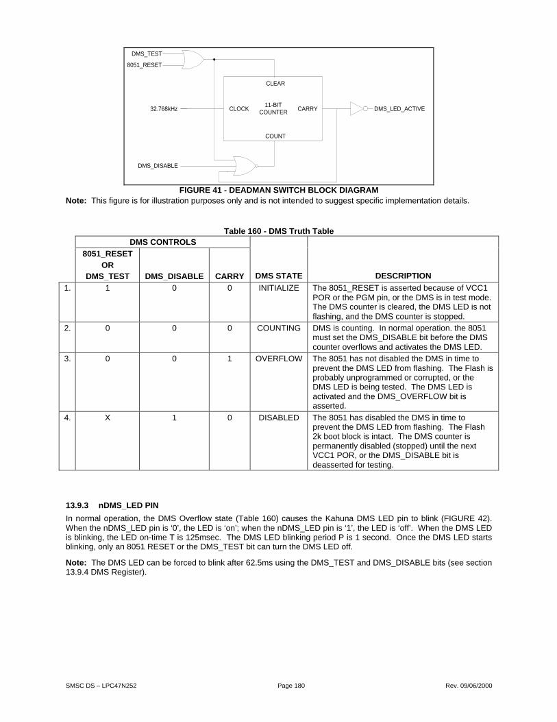
SMSC DS – LPC47N252 Page 180 Rev. 09/06/2000
11-BITCOUNTER
CLEAR
COUNT
CARRYCLOCK DMS_LED_ACTIVE32.768kHz
DMS_DISABLE
8051_RESET
DMS_TEST
FIGURE 41 - DEADMAN SWITCH BLOCK DIAGRAMNote: This figure is for illustration purposes only and is not intended to suggest specific implementation details.
Table 160 - DMS Truth TableDMS CONTROLS
8051_RESET
ORDMS_TEST DMS_DISABLE CARRY DMS STATE DESCRIPTION
1. 1 0 0 INITIALIZE The 8051_RESET is asserted because of VCC1POR or the PGM pin, or the DMS is in test mode.The DMS counter is cleared, the DMS LED is notflashing, and the DMS counter is stopped.
2. 0 0 0 COUNTING DMS is counting. In normal operation. the 8051must set the DMS_DISABLE bit before the DMScounter overflows and activates the DMS LED.
3. 0 0 1 OVERFLOW The 8051 has not disabled the DMS in time toprevent the DMS LED from flashing. The Flash isprobably unprogrammed or corrupted, or theDMS LED is being tested. The DMS LED isactivated and the DMS_OVERFLOW bit isasserted.
4. X 1 0 DISABLED The 8051 has disabled the DMS in time toprevent the DMS LED from flashing. The Flash2k boot block is intact. The DMS counter ispermanently disabled (stopped) until the nextVCC1 POR, or the DMS_DISABLE bit isdeasserted for testing.
13.9.3 nDMS_LED PIN
In normal operation, the DMS Overflow state (Table 160) causes the Kahuna DMS LED pin to blink (FIGURE 42).When the nDMS_LED pin is ‘0’, the LED is ‘on’; when the nDMS_LED pin is ‘1’, the LED is ‘off’. When the DMS LEDis blinking, the LED on-time T is 125msec. The DMS LED blinking period P is 1 second. Once the DMS LED startsblinking, only an 8051 RESET or the DMS_TEST bit can turn the DMS LED off.
Note: The DMS LED can be forced to blink after 62.5ms using the DMS_TEST and DMS_DISABLE bits (see section13.9.4 DMS Register).

SMSC DS – LPC47N252 Page 181 Rev. 09/06/2000
P
T
FIGURE 42 – DMS_LED OUTPUT
13.9.4 DMS REGISTER
The DMS register contains control and status bits for the Kahuna Deadman Switch function (Table 161). The DMSregister is available only to the 8051 at MMCR address 0x7F86 and is cleared by VCC1 POR.
Table 161 - DMS RegisterHOST ADDRESS N/A
8051 ADDRESS 0x7F86
POWER VCC1
DEFAULT 0x00
D7 D6 D5 D4 D3 D2 D1 D0
HOST TYPE - - - - - - - -
8051 TYPE R R R R R R/WC R/W R/W
BIT NAME RESERVED DMS_OVERFLOW DMS_TEST DMS_DISABLE
13.9.4.1 DMS_OVERFLOW Bit – D2
The DMS_OVERFLOW bit indicates that the DMS overflow state has occurred (see Item #3 in Table 160, above).The DMS_OVERFLOW bit is the Carry output of the DMS counter (not shown in FIGURE 41).
When the DMS_OVERFLOW bit is deasserted ‘0’ (default), the DMS overflow state has not occurred or has beencleared. When the DMS_OVERFLOW bit is asserted ‘1’, the DMS overflow state has occurred. TheDMS_OVERFLOW bit is R/WC. To deassert the DMS_OVERFLOW bit, write a ‘1’ to bit D2. The DMS_OVERFLOWbit is also deasserted by VCC1 POR. The DMS_OVERFLOW bit can inform the 8051 that an unprogrammed orcorrupted Flash Boot Block has been restored without a VCC1 POR.
13.9.4.2 DMS_TEST Bit – D1
The DMS_TEST bit along with the DMS_DISABLE bit (D0) can be used to exercise the DMS counter and thenDMS_LED output pin for test purposes because in a properly functioning Kahuna system the DMS_LED output willnever be asserted.
When the DMS_TEST bit is deasserted ‘0’ (default), the DMS test function is disabled. When the DMS_TEST bit isasserted ‘1’, the DMS counter is cleared and disabled (FIGURE 41). The DMS_TEST bit is R/W and deasserted byVCC1 POR. To exercise the nDMS_LED output pin, follow the steps shown in Table 162.
Table 162 - Exercising nDMS_LED Output PinPROCEDURE DESCRIPTION
1. Deassert the DMS_DISABLE bit. During normal boot procedure the 8051 hasasserted the DMS_DISABLE bit before the DMSoverflow state has occurred. The DMS_TEST bitmust remain deasserted.
2. Wait for the DMS_OVERFLOW bit tobe asserted.
When the DMS_DISABLE bit is deasserted, theDMS counter will resume until overflow. When theDMS_OVERFLOW bit is asserted the nDMS_LEDoutput pin should begin pulsing as shown inFIGURE 42.

SMSC DS – LPC47N252 Page 182 Rev. 09/06/2000
PROCEDURE DESCRIPTION
3. Assert the DMS_DISABLE bit. Permanently disable the DMS counter. Providesome means to signal the end of the nDMS_LEDtest.
4. Assert the DMS_TEST bit. When the nDMS_LED test is complete, thenDMS_LED output pin is permanently deassertedwhen the DMS_TEST bit is asserted.
5. Deassert the DMS_OVERFLOW bit. Remove indication that the DMS overflow state hasbeen reached.
13.9.4.3 DMS_DISABLE Bit – D0
The DMS_DISABLE bit D0 is used to permanently stop the DMS counter (FIGURE 41). When the DMS_DISABLE bitis deasserted ‘0’ (default), the DMS counter is enabled and will begin counting until the DMS overflow state isreached, assuming the DMS_TEST bit and the 8051_RESET signal are deasserted. When the DMS_DISABLE bit isasserted ‘1’, the DMS counter is permanently disabled. The DMS_DISABLE bit can be used along with theDMS_TEST bit to exercise the nDMS_LED output pin (see section 13.8.4.2 DMS_TEST Bit – D1, above).
13.10 FLASH PROGRAM REGISTER
The Flash Program register contains the Flash Program Interface Decoder controls (see section 13.2) and theRESET FLASH control.
The Flash Program register is shown in Table 163. The Flash Program register is always available to the LPC Hostand to the 8051.
Table 163 - Flash Program RegisterHOST ADDRESS MBX9Eh
8051 ADDRESS 0x7F35
POWER VCC1
DEFAULT ‘000XXX00’b
D7 D6 D5 D4 D3 D2 D1 D0
HOST TYPE R/W R R R R R R/W R/W
8051 TYPE R/W R R R R R R/W R/W
BIT NAME RESETFLASH
RESERVED FWP PIN EXTFLASH
ATEPGM
LPCPGM
8051PGM
13.10.1 RESET FLASH – D7
The RESET FLASH bit can reset the internal 64k Embedded Flash ROM (see 12.3.3 Reset on page 154). When theRESET FLASH bit is asserted ‘1’, the 64k Embedded Flash ROM is placed in a reset state. When the RESETFLASH bit is de-asserted ‘0’ (default), the 64k Embedded Flash ROM is placed in Read Array mode.
Note: The RESET FLASH bit is not self-clearing.
APPLICATION NOTE: The lowest 8051 system power consumption state is achieved when the 8051 is stopped andthe RESET FLASH bit is asserted. The RESET FLASH bit should only be asserted by the 8051 when the MMC bit is‘1’ and the 8051 is executing out of the Internal Scratch ROM (see section 13.11 Internal Scratch ROM on page 183).
13.10.2 FWP – D4
The FWP Pin bit reflects the status of the nFWP input pin. When nFWP is asserted (‘0’), the boot block in theKahuna Embedded 64K Flash ROM is write-protected and the FWP Pin bit is asserted ‘1’. When the nFWP pin isdeasserted (‘1’), the boot block is writeable and the FWP Pin bit is deasserted ‘0’.
Note: The EXT FLASH bit is read-only and not affected by VCC1 POR.

SMSC DS – LPC47N252 Page 183 Rev. 09/06/2000
13.10.3 EXT FLASH – D3
The EXT FLASH bit in the Flash Program register indicates the state of the Kahuna nEA pin. When the nEA pin isasserted ‘0’, the EXT FLASH bit is asserted ‘1’, when the nEA pin is deasserted ‘1’, the EXT FLASH bit is deasserted‘0’. When the EXT FLASH bit is asserted (‘1’), the Kahuna Flash programming interface is disabled (see Table 152).
13.10.4 ATE PGM – D2
The ATE PGM bit in the Flash Program register directly reflects the state of the Kahuna PGM pin. When the PGM pinis asserted, the ATE PGM bit is asserted, when the PGM pin is deasserted, the ATE PGM bit is deasserted. Whenthe ATE PGM bit is asserted (‘1’), the Kahuna Flash programming interface is dedicated to the ATE Flash ProgramAccess function (see Table 152 and section 13.6 ATE Flash Program Access, above).
Note: The ATE PGM bit is read-only and not affected by VCC1 POR.
13.10.5 LPC PGM – D1
The LPC PGM bit in the Flash Program register is used to enable the LPC Flash Program Access function (see Table152 and section 13.5 LPC Bus Flash Program Access, above). The LPC PGM bit can only be asserted when theATE PGM and the 8051 PGM bits are deasserted ‘0’ (Table 152), and the SYSTEM FLASH bit in the Disable registeris deasserted. When the LPC PGM bit is asserted ‘1’, the Kahuna 64k Embedded Flash is dedicated to the LPC Hostprogramming interface. The LPC PGM bit is read/write and deasserted by VCC1 POR.
13.10.6 8051 PGM – D0
The 8051 PGM bit in the Flash Program register is used to enable the 8051 Program Access function (see Table 152and section 13.3 8051 Code Fetch Access, above). The 8051 PGM bit can only be asserted when the ATE PGM bitis deasserted ‘0’; the 8051 PGM bit overrides the LPC PGM bit (Table 152).
When the 8051 PGM bit is asserted ‘1’, the Kahuna 64k Embedded Flash is dedicated to the 8051 programminginterface. The 8051 PGM bit is read/write and deasserted by VCC1 POR.
13.11 8051/LPC FLASH PROGRAM ACCESS REGISTERS
The 8051/LPC Flash Program Access registers are used by the 8051 and the LPC Host to program the Kahuna 64kEmbedded Flash (see FIGURE 33 on page 172). To the 8051, the 8051/LPC Flash Program Access registers areaccessed using memory-mapped control registers; to the LPC host, the 8051/LPC Flash Program Access registersare accessed using the Mailbox Registers Interface. For information regarding the 8051 and LPC Flash ProgramAccess functions see section 13.4 8051 Flash Program Access on page 171 and section 13.5 LPC Bus FlashProgram Access on page 172. The 8051 and LPC Flash Program Access functions are enabled by the FlashProgram Interface Decoder (see section 13.2 Flash Program Interface Decoder).
When the 8051 is using the 8051/LPC Flash Program Access interface, LPC Host access is disabled. The LPC Hostwill be able to read the contents of the 8051/LPC Flash Program Access registers, but it will not be able to write theseregisters and reads to the Flash Data register will return the contents of the Flash Data register but will not read-activate the Flash CSI interface.
When the LPC Host is using the 8051/LPC Flash Program Access interface, 8051 access is disabled. Typically,when LPC Host is using the 8051/LPC Flash Program Access interface the 8051 is stopped.
Note: The LPC Host must stop the 8051 to use the 8051/LPC Flash Program Access interface.
13.11.1 FLASH HIGH ADDRESS REGISTER
The Flash High Address register contains Flash address bits A15 – A8 (Table 164). The LPC Host can access theFlash High Address register using the Mailbox Registers Interface address 0x9F. The 8051 can access the FlashHigh Address register using MMCR address 0x7FB0.
Note: To properly access the Kahuna 64k Embedded Flash, the Flash High Address and the Flash Low Addressregisters must be initialized before reading or writing the Flash Data register.

SMSC DS – LPC47N252 Page 184 Rev. 09/06/2000
Table 164 - Flash High Address RegisterHOST ADDRESS MBX9Fh
8051 ADDRESS 0x7FB0
POWER VCC1
DEFAULT 0x00
D7 D6 D5 D4 D3 D2 D1 D0
HOST TYPE R/W R/W R/W R/W R/W R/W R/W R/W
8051 TYPE R/W R/W R/W R/W R/W R/W R/W R/W
BIT NAME A15 A14 A13 A12 A11 A10 A9 A8
13.11.2 FLASH LOW ADDRESS REGISTER
The Flash Low Address register contains Flash address bits A7 – A0 (Table 165). The LPC Host can access theFlash Low Address register using the Mailbox Registers Interface address 0x80. The 8051 can access the Flash LowAddress register using MMCR address 0x7FB1.
Note: To properly access the Kahuna 64k Embedded Flash, the Flash High Address and the Flash Low Addressregisters must be initialized before reading or writing the Flash Data register.
Table 165 - Flash Low Address RegisterHOST ADDRESS MBX80h
8051 ADDRESS 0x7FB1
POWER VCC1
DEFAULT 0x00
D7 D6 D5 D4 D3 D2 D1 D0
HOST TYPE R/W R/W R/W R/W R/W R/W R/W R/W
8051 TYPE R/W R/W R/W R/W R/W R/W R/W R/W
BIT NAME A7 A6 A5 A4 A3 A2 A1 A0
13.11.3 FLASH DATA REGISTER
The Flash Data register contains either the Kahuna 64k Embedded Flash data, CSI command-codes, or the contentsof the CSI Status register (Table 166). The LPC Host can access the Flash Data register using the Mailbox RegisterInterface address 0x81. The 8051 can access the Flash Data register using MMCR address 0x7FB2.
Note: To properly access the Kahuna 64k Embedded Flash, the Flash High Address and the Flash Low Addressregisters must be initialized before reading or writing the Flash Data register.
Table 166 - Flash Data RegisterHOST ADDRESS MBX81h
8051 ADDRESS 0x7FB2
POWER VCC1
DEFAULT 0x00
D7 D6 D5 D4 D3 D2 D1 D0
HOST TYPE R/W R/W R/W R/W R/W R/W R/W R/W
8051 TYPE R/W R/W R/W R/W R/W R/W R/W R/W
BIT NAME D7 D6 D5 D4 D3 D2 D1 D0

SMSC DS – LPC47N252 Page 185 Rev. 09/06/2000
13.12 INTERNAL SCRATCH ROM
The Kahuna 8051 can execute program code from a 256-byte Internal Scratch ROM when the MMC bit is ‘1’. TheMMC bit is D3 in CONFIGURATION REGISTER 0 (MMCR 0x7FF4). The Configuration Register 0 register isdescribed in the section see 11.8.3.4.
When the MMC bit is ‘1’, the 8051 can execute out of the Internal Scratch ROM either when the 8051 Code FetchAccess interface or when the 8051 Program Access interface is selected. For example, the 8051 can execute codefrom the Internal Scratch ROM even when the 8051 Code Fetch Interface is unselected by the Flash ProgramInterface Decoder (see section 13.2 Flash Program Interface Decoder, above). When the MMC bit = ‘0’, there is 256bytes of Internal Scratch RAM located at address 0x7D00 in the 8051 Data Space (FIGURE 43). When the MMC bitis ‘1’, the Internal Scratch RAM becomes Internal Scratch ROM and occupies 256 bytes at the top of the 64k codespace; i.e., FF00h – FFFFh (FIGURE 44).
Note: When the 8051 is running from external flash, i.e. when the nEA pin = ‘0’, the MMC bit must be ‘0’.
Program Memory Data Memory
External Internal
SFR (Direct Only)
Direct and Indirect
Indirect Only
00h
80h
7D00h
7E00h
7F00h
7FFFhM/M Registers
RAM
Scratch RAM
FFFFh
MMC bit = 0
64K
FFh 80h
FFh
0000h
External
FIGURE 43 - KAHUNA MEMORY MAP W/INTERNAL SCRATCH RAM (MMC BIT = '0')
Program Memory Data Memory
External Internal
SFR (Direct Only)
Direct and Indirect
Indirect Only
00h
80h
7D00h
7E00h
7F00h
7FFFhM/M Registers
RAM
FFFFh
MMC bit = 1
64K − 256
Scratch ROMInternal
FFh 80h
FFh
FF00h
0000h
External
FIGURE 44 - KAHUNA MEMORY MAP W/INTERNAL SCRATCH ROM (MMC BIT = '1')

SMSC DS – LPC47N252 Page 186 Rev. 09/06/2000
14 WATCH DOG TIMER
14.1 WDT OPERATION
When enabled, the Watch Dog Timer (WDT) circuit will generate a system reset if the user program fails toreload the watchdog timer (WDT) within a specified length of time known as the ‘watchdog interval’.
The WDT consists of an 8-bit timer (WDT) with a 9-bit prescaler. The prescaler is fed with 32 KHz whichalways runs, even if the 8051 is in SLEEP state. The 8 bit WDT timer is decremented every (1/32KHz) *512seconds or 16.0 ms. Thus, the watchdog interval is programmable between 16ms and 4.08 seconds on16ms intervals.
14.2 WDT ACTION
If the 8 bit timer (WDT) underflows, a VCC1 POR is generated
8051 in Idle Mode - WDT will be active if enabled. When the WDT timer underflows in idle mode, the 8051will be reset. It is up to the firmware engineer to design code that uses a timer to generate an interrupt thatwill exit idle mode and re-initialize the WDT timer and then put the 8051 back into idle mode.
8051 in Sleep Mode - If enabled, the WDT is active since it is running off of the 32 KHz clock. Therefore, ifthe WDT is enabled the 8051 should never remain in the SLEEP state for more than 4 seconds.
14.3 WDT ACTIVATION
Upon VCC1 POR the Watch Dog Timer powers up inactive. The Watch Dog Timer is activated when theWDT enable bit (WDT CONTROL bit D1) is set by 8051 firmware. The WDT may be disabled undersoftware control through a specific sequence. Software can clear the SDT enable bit by:
§ Setting the WLE-WDT Load enable bit in the WDT Control/Status Register.
§ Writing 00h to the WDT Timer Register (this causes the WDT Enable and the WLE_WDT Load Enablebits to each reset to 0).
Once the WDT has been activated, this sequence must be executed in order to disable watchdog operationvia software control.
Note: Since a VCC1 POR will reset the WDT enable bit, the WDT must be re-enabled after eachoccurrence.
14.4 WDT RESET MECHANISM
The watchdog timer (WDT) must be reloaded within periods that are shorter than the programmed watchdoginterval; otherwise the WDT will underflow and a VCC1 POR will be generated. It is the responsibility ofthe user program to continually execute sections of code which reload the 8 bit timer (WDT).
The WDT is reloaded in two stages in order to prevent erroneous software from reloading the watchdog.First WDT CONTROL bit D0 (WLE-WDT Load Enable) must be set. Then the WDT may be loaded. Whenthe WDT is loaded WLE is automatically reset. WDT can not be loaded when WLE is reset. Since the WDTtimer is a down counter, a reload value of 01h results in the minimum WDT interval (16ms) and a reloadvalue of 0FFh results in the maximum WDT interval (4.08 seconds). Loading 00h into the WDT disables theWDT and clears the WDT Enable bit. Note, the 9 bit prescaler is initialized whenever the WDT timer isloaded.

SMSC DS – LPC47N252 Page 187 Rev. 09/06/2000
14.5 WDT MEMORY MAPPED REGISTERS
Table 167 - WDTHOST ADDRESS N/A
8051 ADDRESS 0x 7F38
POWER VCC1
DEFAULT 0xFF
D7 D6 D5 D4 D3 D2 D1 D0
8051 R/W R/W R/W R/W R/W R/W R/W R/W R/W
SYSTEM R/W N/A N/A N/A N/A N/A N/A N/A N/A
BIT DEF WDTTimer
WDTTimer
WDTTimer
WDTTimer
WDTTimer
WDTTimer
WDTTimer
WDTTimer
Table 168 - WDT Control/StatusHOST ADDRESS N/A
8051 ADDRESS 0x 7F37
POWER VCC1
DEFAULT 0x00
D7-D2 D1 D0
8051 R/W R R/W R/W
SYSTEM R/W N/A N/A N/A
BIT DEF Reserved WDT Enable WLE-WDT Load Enable
WLEWatchdog Load Enable bit must be set to enable writing to the WDT Timer register. This bit is automaticallyreset when the 8051 writes to the WDT register. If this bit is reset, writes to the WDT register are ignored.
WDT EnableThe WDT enable bit must be set by 8051 firmware to enable or start the Watch Dog Timer. A VCC1 POR orthe above described software sequence will reset this bit.
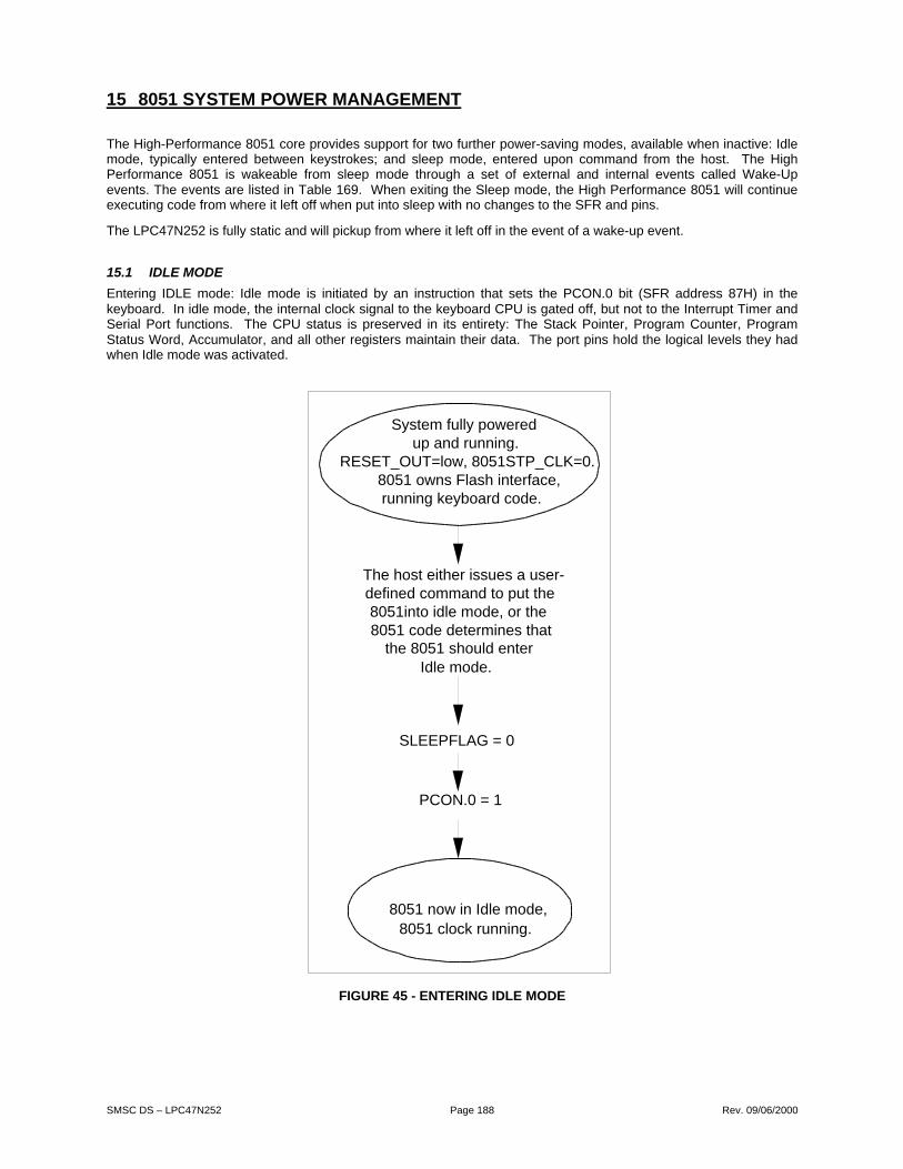
SMSC DS – LPC47N252 Page 188 Rev. 09/06/2000
15 8051 SYSTEM POWER MANAGEMENT
The High-Performance 8051 core provides support for two further power-saving modes, available when inactive: Idlemode, typically entered between keystrokes; and sleep mode, entered upon command from the host. The HighPerformance 8051 is wakeable from sleep mode through a set of external and internal events called Wake-Upevents. The events are listed in Table 169. When exiting the Sleep mode, the High Performance 8051 will continueexecuting code from where it left off when put into sleep with no changes to the SFR and pins.
The LPC47N252 is fully static and will pickup from where it left off in the event of a wake-up event.
15.1 IDLE MODE
Entering IDLE mode: Idle mode is initiated by an instruction that sets the PCON.0 bit (SFR address 87H) in thekeyboard. In idle mode, the internal clock signal to the keyboard CPU is gated off, but not to the Interrupt Timer andSerial Port functions. The CPU status is preserved in its entirety: The Stack Pointer, Program Counter, ProgramStatus Word, Accumulator, and all other registers maintain their data. The port pins hold the logical levels they hadwhen Idle mode was activated.
FIGURE 45 - ENTERING IDLE MODE
System fully poweredup and running.
RESET_OUT=low, 8051STP_CLK=0.8051 owns Flash interface,running keyboard code.
8051 now in Idle mode,8051 clock running.
The host either issues a user-defined command to put the8051into idle mode, or the8051 code determines that
the 8051 should enter Idle mode.
SLEEPFLAG = 0
PCON.0 = 1

SMSC DS – LPC47N252 Page 189 Rev. 09/06/2000
FIGURE 46 - EXITING IDLE MODE DUE TO IRQ
15.1.1 EXITING IDLE MODE
There are two ways to terminate Idle mode. First, activation of any enabled interrupt will cause the PCON.0 bit to becleared by hardware. The interrupt will be serviced and, following the RETI, the CPU will resume operation byexecuting the instruction following the one that put the CPU into Idle mode.
The second way to terminate the Idle mode is with a VCC1 POR. Note that a VCC1 POR will clear the registers.The CPU will not resume program execution from where it left off.
15.2 SLEEP MODE
When the CPU enters sleep mode, all internal clocks, including the core clocks, are turned off. If an external crystalis used, the internal oscillator is turned off. RAM contents are preserved. Sleep mode is initiated by a user defined8051 command sequence.
Sleep Mode Sequence - To enter sleep mode, the 8051:
Turns on the ring oscillator (KSTP_CLK[4] = 1)
Switches the clock source (KSTP_CLK[5] = 0)
Turns off the clock chip (or the whole system power, VCC2)
Masks all interrupts except for INT5_h
Sets SLEEPFLAG = 1
Sets PCON.0 = 1
The ring oscillator will be automatically turned off
The 8051 goes into Sleep mode.
Unmasked8051 IRQ ?
N
8051 returns to executingfrom where it left off prior to
entering Idle mode.
(Note)
8051 in Idle mode,
8051 clock running.
Note: In order to leave idle mode the 8051 must receive an interrupt, typicallya software timer interrupt will be used.
Y
8051 leaves Idle mode,executes IRQ service routinecode and executes an IRET
when done.

SMSC DS – LPC47N252 Page 190 Rev. 09/06/2000
In sleep mode, the FDC, UART and parallel port are powered off if VCC2 is removed, but the RTC and 8051 are inpowerdown (sleep) mode. In Sleep mode the LPC47N252 consumes less than 20µA, and all wake-up pins are stillactive.
When the 8051 is in sleep mode, all of the clocks are stopped and the 8051 is waiting for an unmasked wake-upevent. When the wake-up event occurs, the ring oscillator is started the 8051 starts executing from where it stoppedin the sleep Mode Sequence. Once running, the 8051 can access all of the registers that are on VCC1 and if VCC2is at 3.3V it can access all of the registers on VCC2. The 8051 running from the ring oscillator (internal) clock sourceswitch to an external clock source and then turn off the ring oscillator (internal) clock source.
System fully powered up and running.
RESET_OUT= low, 8051STP_CLK= 0.8051 owns Flash interface,running keyboard code.
8051 now insleep mode,
8051 clock stopped.
The host either issues a user-defined command to put the
8051into sleep mode, orthe 8051 code determinesthat the 8051 should enter
sleep mode.
SLEEPFLAG = 1
PCON.0 = 1
8051 switches its clock sourceto the ring oscillator.
8051 masks all interruptsexcept for T5INT.
Ring oscillator first gated offfrom 8051, then turned off.
The 8051 may/may not turnoff VCC2 to rest of system.
FIGURE 47 - ENTERING SLEEP MODE

SMSC DS – LPC47N252 Page 191 Rev. 09/06/2000
8051 in sleep mode.RTC, 8051 and other VCC1driven pins are active
UnmaskedWake-upEvent ?
N
Y
INT5_N generated.Turn on ring oscillator.
SLEEPFLAG = 0.
Once stabilized, the ringoscillator is gated through to
the 8051.
The 8051 is now running inIdle mode and respondsimmediately to T5INT.
8051 returns to executingfrom where it left off prior to
entering sleep mode.
8051 leaves Idle mode,executes int5_n service
routine (disables int5_n) andexecutes an IRET when
done.
Wake Up EventsRTC Alarm,Power Button,Ring Indicator,etc.
FIGURE 48 - EXITING SLEEP MODE
15.3 WAKE-UP EVENTS
There are two types of wake-up events that can occur, internal (Table 169 – Internal System Wake-up Events) andexternal (Table 170 - External System Wake-up Events). Wake-up events on General Purpose Pins can be eitheredge or selectable edges. Refer to table Table 129 For further description. Wake-up events can occur when VCC2is off. VCC1 must be on for a wake-up event to occur, but the high-performance 8051 can be in sleep mode.

SMSC DS – LPC47N252 Page 192 Rev. 09/06/2000
Table 169 – Internal System Wake-up EventsWAKE-UPEVENTS REGISTER DESCRIPTION
RTC_ALRM Wake Up Src 1(0x7F2B) [D0]
RTC alarm
HTIMER Wake Up Src 2(0x7F2B) [D2]
Hibernation timer
PM1_STS2 Wake Up Src 1(0x7F2A) [D5]
PM1 Status
PM1_EN2 Wake Up Src 1(0x7F2A) [D6]
PM1 Enable
PM1_CTL2 Wake Up Src 1(0x7F2A) [D7]
PM1 Control
Table 170 - External System Wake-up Events
PIN WAKE-UPEVENTS
ACTIVE EDGE REGISTER DESCRIPTION
nRI UART_RI1 Edge, high-to-low Wake Up Src 2(0x7F2B) [D6]
UART ring indicator
AB1_DATA
ACCBUS1 Wake Up Src1(0x7F2A) [D4]
AB_DAT
ACCESS BUS1
AB2_DATA
ACCBUS2Leading edge, high-to-low
Wake Up Src1
(0x7F2A) [D3]
AB_DAT
ACCESS BUS2
IRRX IR_RX Edge, high-to-low Wake Up Src1(0x7F2B) [D2]
IR energy detected on theIRRX Receive pin.
KSI[7:0] WK_ANYKEY Edge, high-to-low Wake Up Src 2(0x7F2B) [D1]
Any Keyboard Key pressed
GPIO0/ WK_SE02 Wake Up Src 4(0x7F59) [D2]
GPIO1 WK_SE03 Wake Up Src 4(0x7F59) [D3]
GPIO2 WK_SE04 Wake Up Src 4(0x7F59) [D4]
GPIO3 TRIGGER INT SRC 1(0x7F02) [D3]
GPIO4 WK_SE07 Wake Up Src 4(0x7F59) [D7]
GPIO5 WK_SE10
PROGRAMMABLE
Wake Up Src 5(0x7F5E) [D0]
General Purpose Pin
GPIO6 WK_SE11 Wake Up Src 5(0x7F5E) [D1]
General Purpose Pin
Or FIR Mode Output/ 2nd
Receive Input
GPIO7 WK_SE06 Wake Up Src 4(0x7F59) [D6]
General Purpose Pin
GPIO8 WK_SE12 Wake Up Src 5(0x7F5E) [D2]
GPIO8 or IR energy detectedon the GPIO/COM-RXReceive pin.
GPIO9 WK_SE13 Wake Up Src 5(0x7F5E) [D3]
General Purpose Pin
GPIO10 WK_SE14 Wake Up Src 5(0x7F5E) [D4]
General Purpose Pin
Or FIR Mode Output/ 2nd
Receive Input
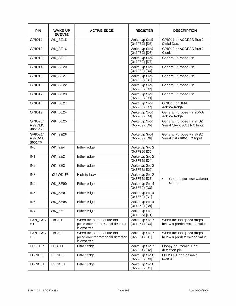
SMSC DS – LPC47N252 Page 193 Rev. 09/06/2000
PIN WAKE-UPEVENTS
ACTIVE EDGE REGISTER DESCRIPTION
GPIO11 WK_SE15 Wake Up Src5(0x7F5E) [D5]
GPIO11 or ACCESS.Bus 2Serial Data
GPIO12 WK_SE16 Wake Up Src5(0x7F5E) [D6]
GPIO12 or ACCESS.Bus 2Clock
GPIO13 WK_SE17 Wake Up Src5(0x7F5E) [D7]
General Purpose Pin
GPIO14 WK_SE20 Wake Up Src6(0x7F63) [D0]
General Purpose Pin
GPIO15 WK_SE21 Wake Up Src6(0x7F63) [D1]
General Purpose Pin
GPIO16 WK_SE22 Wake Up Src6(0x7F63) [D2]
General Purpose Pin
GPIO17 WK_SE23 Wake Up Src6(0x7F63) [D3]
General Purpose Pin
GPIO18 WK_SE27 Wake Up Src6(0x7F63) [D7]
GPIO18 or DMAAcknowledge
GPIO19 WK_SE24 Wake Up Src6(0x7F63) [D4]
General Purpose Pin /DMAAcknowledge
GPIO20/PS2CLK/8051RX
WK_SE25 Wake Up Src6(0x7F63) [D5]
General Purpose Pin /PS2Serial Clock 8051 RX Input
GPIO21/PS2DAT/8051TX
WK_SE26 Wake Up Src6(0x7F63) [D6]
General Purpose Pin /PS2Serial Data 8051 TX Input
IN0 WK_EE4 Either edge Wake Up Src 2(0x7F2B) [D5]
IN1 WK_EE2 Either edge Wake Up Src 2(0x7F2B) [D4]
IN2 WK_EE3 Either edge Wake Up Src 2(0x7F2B) [D5]
IN3 nGPWKUP High-to-Low Wake Up Src 2(0x7F2B) [D3]
IN4 WK_SE00 Either edge Wake Up Src 4(0x7F59) [D0]
IN5 WK_SE01 Either edge Wake Up Src 4(0x7F59) [D1]
IN6 WK_SE05 Either edge Wake Up Src 4(0x7F59) [D5]
IN7 WK_EE1 Either edge Wake Up Src1(0x7F2B) [D1]
§ General purpose wakeupsource
FAN_TACH1
TACH1 When the output of the fanpulse counter threshold detectoris asserted.
Wake Up Src 7(0x7F64) [D0]
When the fan speed dropsbelow a predetermined value.
FAN_TACH2
TACH2 When the output of the fanpulse counter threshold detectoris asserted.
Wake Up Src 7(0x7F64) [D1]
When the fan speed dropsbelow a predetermined value.
FDC_PP FDC_PP Either edge Wake Up Src 7(0x7F64) [D2]
Floppy-on-Parallel Portdetection pin.
LGPIO50 LGPIO50 Either edge Wake Up Src 8(0x7F55) [D0]
LGPIO51 LGPIO51 Either edge Wake Up Src 8(0x7F55) [D1]
LPC/8051-addressableGPIOs
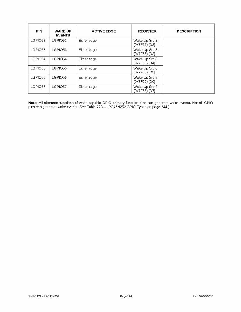
SMSC DS – LPC47N252 Page 194 Rev. 09/06/2000
PIN WAKE-UPEVENTS
ACTIVE EDGE REGISTER DESCRIPTION
LGPIO52 LGPIO52 Either edge Wake Up Src 8(0x7F55) [D2]
LGPIO53 LGPIO53 Either edge Wake Up Src 8(0x7F55) [D3]
LGPIO54 LGPIO54 Either edge Wake Up Src 8(0x7F55) [D4]
LGPIO55 LGPIO55 Either edge Wake Up Src 8(0x7F55) [D5]
LGPIO56 LGPIO56 Either edge Wake Up Src 8(0x7F55) [D6]
LGPIO57 LGPIO57 Either edge Wake Up Src 8(0x7F55) [D7]
Note: All alternate functions of wake-capable GPIO primary function pins can generate wake events. Not all GPIOpins can generate wake events (See Table 228 – LPC47N252 GPIO Types on page 244.)

SMSC DS – LPC47N252 Page 195 Rev. 09/06/2000
16 KEYBOARD CONTROLLER
16.1 8042 STYLE HOST INTERFACE
The LPC47N252 keyboard controller uses a High-Performance 8051 microcontroller CPU core to produce a supersetof the features provided by the industry-standard 8042 keyboard controller. Added features include two high-driveserial interfaces, and additional interrupt sources. The LPC47N252 provides an industry standard 8042-style LPChost interface to the High-Performance 8051 to emulate standard 8042 keyboard controller and preserve softwarebackward compatibility with the system BIOS.
The LPC47N252’s LPC keyboard interface is functionally compatible with the 8042-style host interface. keyboardcontroller has the KBD (Keyboard) Status register, KBD Data/Command Write register, and KBD Data Read register.
Table 171 shows how the has the LPC interface accesses the keyboard controller. In addition to the above signals,the host interface includes keyboard and mouse interrupts.
16.2 KEYBOARD CONTROLLER REGISTER DESCRIPTION
Table 171 - Keyboard Controller LPC I/O Address MapISA ADDRESS COMMAND FUNCTION
0x60 Write Keyboard Data Write (C/D=0)
Read Keyboard Data Read
0x64 Write Keyboard Command Write (C/D=1)
Read Keyboard Status Read
Note: These registers consist of three separate 8 bit registers: KBD Status, KBD Data/Command Write and KBDData Read.
16.2.1 KEYBOARD DATA WRITE
This is an 8 bit write only register. When written, the C/D status bit of the status register is cleared to zero and theIBF bit is set.
16.2.2 KEYBOARD DATA READ
This is an 8 bit read only register. When read, the PBOBF and/or AUXOBF interrupts are cleared and the OBF flag inthe status register is cleared.
16.2.3 KEYBOARD COMMAND WRITE
This is an 8 bit write only register. When written, the C/D status bit of the status register is set to one and the IBF bitis set.
16.2.4 KEYBOARD STATUS READ
This is an 8 bit read only register. Refer to the description of the Status Register (7FF2H) for more information.
16.3 8051-TO-HOST KEYBOARD COMMUNICATION
The 8051 can write to the KBD Data Read register via address 7FF1H and 7FFAH (Aux Host Data Register)respectively. A write to either of these addresses automatically sets bit 0 (OBF) in the Status register. A write to7FF1H also sets PCOBF. A write to 7FFAH also sets AUXOBF1. See Table 172 below.
Table 172 - Host-Interface Flags8051
ADDRESS FLAG
7FF1H (R/W) PCOBF (KIRQ) output signal goes high
7FFAH (W) AUXOBF1 (MIRQ) output signal goes high

SMSC DS – LPC47N252 Page 196 Rev. 09/06/2000
Table 173 - Host I/F Data RegisterHOST 0x60
8051 0x7FF1
POWER VCC1
DEFAULT N/A
The Input Data register and Output Data register are each 8 bits wide. A write to this 8 bit register by the 8051 willload the Keyboard Data Read Buffer, set the OBF flag and set the PCOBF output if enabled. A read of this registerby the 8051 will read the data from the Keyboard Data or Command Write Buffer and clear the IBF flag. Refer to thePCOBF and Status register descriptions for more information.
Table 174 - Host I/F Command RegisterHOST 0x64 (W)
8051 0x7FF1
POWER VCC1
DEFAULT N/A
The host CPU sends commands to the keyboard controller by writing command bytes to this register.
Table 175 - Host I/F Status RegisterHOST 0x64 (R)
8051 0x7FF2
POWER VCC1
DEFAULT N/A
The Status register is 8 bits wide. Shows the contents of the KBD Status register.
Table 176 - KBD Status RegisterD7 D6 D5 D4 D3 D2 D1 D0
UD UD AUXOBF/UD UD C/D UD IBF OBF
This register is read-only for the Host and read/write by the 8051. The 8051 cannot write to bits 0, 1, or 3 of theStatus register.
UDRead/Writeable by 8051. These bits are user-definable.
C/DCommand Data - This bit specifies whether the input data register contains data or a command (“0” = data, “1” =command). During a host data/command write operation, this bit is set to "1" if SA2 = “1” or reset to "0" if SA2 = 0.
IBFInput Buffer Full - This flag is set to “1” whenever the host system writes data into the input data register. Setting thisflag activates the 8051's nIBF interrupt if enabled. When the 8051 reads the input data register, this bit isautomatically reset and the interrupt is cleared. There is no output pin associated with this internal signal.
OBFOutput Buffer Full - This flag is set to “1” whenever the 8051 writes into the data registers at 7FF1H or 7FFAH.When the host system reads the output data register, this bit is automatically reset.
AUXOBFAuxiliary Output Buffer Full - This flag is set to “1” whenever the 8051 writes into the data registers at 7FFAH. Thisflag is reset to “0” whenever the 8051 writes into the data registers at 7FF1H.

SMSC DS – LPC47N252 Page 197 Rev. 09/06/2000
Table 177 - PCOBFHOST N/A
8051 0x7FFD
POWER VCC1
DEFAULT 0x00
Refer to the PCOBF description for information on this register. This is a “1” bit register (bits 1-7=0 on read)
16.4 HOST-TO 8051 KEYBOARD COMMUNICATION
The host system can send both commands and data to the KBD Data/Command Write register. The CPUdifferentiates between commands and data by reading the value of bit 3 of the Status register. When bit 3 is "1", theCPU interprets the register contents as a command. When Bit 3 is "0", the CPU interprets the register contents asdata. During a host write operation, bit 3 is set to "1" if SA2 = 1 or reset to "0" if SA2 = 0.
16.4.1 PCOBF DESCRIPTION
(The following description assumes that OBFEN = 1 in Configuration Register 0); PCOBF is gated onto KIRQ. TheKIRQ signal is a system interrupt which signifies that the 8051 has written to the KBD Data Read register via address7FF1H. On power-up, PCOBF is reset to 0. PCOBF will normally reflect the status of writes to 7FF1H, if PCOBFEN(bit 2 of Configuration register “0”) = “0”. (KIRQ is normally selected as IRQ1 for keyboard support.) PCOBF iscleared by hardware on a read of the Host Data Register.
Additional flexibility has been added which allows firmware to directly control the PCOBF output signal, independentof data transfers to the host-interface data output register. This feature allows the LPC47N252 to be operated viathe host "polled" mode. This firmware control is active when PCOBFEN = 1 and firmware can then bring PCOBFhigh by writing a "1" to the LSB of the 1 bit data register, PCOBF, allocated at 7FFDH. The firmware must also clearthis bit by writing a "0" to the LSB of the 1 bit data register at 7FFDH.
The PCOBF register is also readable; bits 1-7 will return a "0" on the read back. The value read back on bit 0 of theregister always reflects the present value of the PCOBF output. If PCOBFEN = 1, then this value reflects the output ofthe firmware latch at 7FFDH. If PCOBFEN = 0, then the value read back reflects the in-process status of write cyclesto 7FF1H (i.e., if the value read back is high, the host interface output data register has just been written to). IfOBFEN=0, then KIRQ is driven inactive (low).
16.4.2 AUXOBF1 DESCRIPTION
(The following description assumes that OBFEN = 1 in Configuration Register 0); This bit is multiplexed onto MIRQ.The AUXOBF1/MIRQ signal is a system interrupt which signifies that the 8051 has written to the output data registervia address 7FFAH.
On power-up, after VCC1 POR, AUXOBF1 is reset to 0. AUXOBF1 will normally reflects the status of writes to7FFAH. (MIRQ is normally selected as IRQ12 for mouse support.) AUXOBF1 is cleared by hardware on a read ofthe Host Data Register. If OBFEN=0, then KIRQ is driven inactive (low).
HOST I/F STATUS REGISTER BITS
Write to Register AUXOBF (D5) OBF (D0) OBFEN=0 OBFEN=1
7FF1 0 1 KIRQ=0 KIRQ=1
7FFA 1 1 MIRQ=0 MIRQ=1
OBFEN PCOBFEN
0 X KIRQ is inactive and driven low
1 0 KIRQ = PCOBF@7FF1
1 1 KIRQ = PCOBF@7FFD
OBFEN AUXH
0 X MIRQ is inactive and driven low
1 0 MIRQ = PCOBF@7FFA; Status Register D5 = User Defined
1 1 MIRQ = PCOBF@7FFA; Status Register D5 = Hardware Controlled
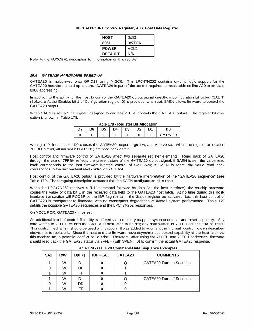
SMSC DS – LPC47N252 Page 198 Rev. 09/06/2000
8051 AUXOBF1 Control Register, AUX Host Data Register
HOST 0x60
8051 0x7FFA
POWER VCC1
DEFAULT N/A
Refer to the AUXOBF1 description for information on this register.
16.5 GATEA20 HARDWARE SPEED-UP
GATEA20 is multiplexed onto GPIO17 using MISC6. The LPC47N252 contains on-chip logic support for theGATEA20 hardware speed-up feature. GATEA20 is part of the control required to mask address line A20 to emulate8086 addressing.
In addition to the ability for the host to control the GATEA20 output signal directly, a configuration bit called "SAEN"(Software Assist Enable, bit 1 of Configuration register 0) is provided; when set, SAEN allows firmware to control theGATEA20 output.
When SAEN is set, a 1 bit register assigned to address 7FFBH controls the GATEA20 output. The register bit allo-cation is shown in Table 178.
Table 178 - Register Bit AllocationD7 D6 D5 D4 D3 D2 D1 D0
x x x x x x x GATEA20
Writing a "0" into location D0 causes the GATEA20 output to go low, and vice versa. When the register at location7FFBH is read, all unused bits (D7-D1) are read back as "0".
Host control and firmware control of GATEA20 affect two separate register elements. Read back of GATEA20through the use of 7FFBH reflects the present state of the GATEA20 output signal: if SAEN is set, the value readback corresponds to the last firmware-initiated control of GATEA20; if SAEN is reset, the value read backcorresponds to the last host-initiated control of GATEA20.
Host control of the GATEA20 output is provided by the hardware interpretation of the "GATEA20 sequence" (seeTable 179). The foregoing description assumes that the SAEN configuration bit is reset.
When the LPC47N252 receives a "D1" command followed by data (via the host interface), the on-chip hardwarecopies the value of data bit 1 in the received data field to the GATEA20 host latch. At no time during this host-interface transaction will PCOBF or the IBF flag (bit 1) in the Status register be activated; i.e., this host control ofGATEA20 is transparent to firmware, with no consequent degradation of overall system performance. Table 179details the possible GATEA20 sequences and the LPC47N252 responses.
On VCC1 POR, GATEA20 will be set.
An additional level of control flexibility is offered via a memory-mapped synchronous set and reset capability. Anydata written to 7FFEH causes the GATEA20 host latch to be set; any data written to 7FFFH causes it to be reset.This control mechanism should be used with caution. It was added to augment the "normal" control flow as describedabove, not to replace it. Since the host and the firmware have asynchronous control capability of the host latch viathis mechanism, a potential conflict could arise. Therefore, after using the 7FFEH and 7FFFH addresses, firmwareshould read back the GATEA20 status via 7FFBH (with SAEN = 0) to confirm the actual GATEA20 response.
Table 179 - GATE20 Command/Data Sequence Examples
SA2 R/W D[0:7] IBF FLAG GATEA20 COMMENTS
1
01
W
WW
D1
DFFF
0
00
Q
11
GATEA20 Turn-on Sequence
101
WWW
D1DDFF
000
Q00
GATEA20 Turn-off Sequence

SMSC DS – LPC47N252 Page 199 Rev. 09/06/2000
SA2 R/W D[0:7] IBF FLAG GATEA20 COMMENTS
11
01
WW
WW
D1D1
DFFF
00
00
11
GATEA20 Turn-on Sequence(*)
1
10
1
W
WW
W
D1
D1DD
FF
0
00
0
Q
Q0
0
GATEA20 Turn-off Sequence(*)
11
1
WW
W
D1XX**
FF
01
1
Q
Invalid Sequence
Notes:1) All examples assume that the SAEN configuration bit is 0.2) "Q" indicates the bit remains set at the previous state.3) *Not a standard sequence.4) **XX = Anything except D1.5) If multiple data bytes, set IBF and wait at state 0. Let the software know something unusual happened.6) For data bytes SA2=0, only D[1] is used; all other bits are don't care.
16.5.1 8051 GATEA20 CONTROL REGISTERS
Table 180 - GATEA20HOST N/A
8051 0x7FFB
POWER VCC1
DEFAULT 0x01Refer to the GATEA20 Hardware Speed-up description for information on this register. This is a one bit register (Bits1-7=0 on read)
Table 181 - SETGA20LHOST N/A
8051 0x7FFE (W)
POWER VCC1
DEFAULT N/ARefer to the GATEA20 Hardware Speed-up description for information on this register. A write to this register setsGateA20.
Table 182 - RSTGA20LHOST N/A
8051 0x7FFF (W)
POWER VCC1
DEFAULT N/ARefer to the GATEA20 Hardware Speed-up description for information on this register. A write to this register re-setsGateA20.

SMSC DS – LPC47N252 Page 200 Rev. 09/06/2000
64&nAEN
SD[7:0] = D1
DFF
DFE
nAEN&60
After D1
nIOW
D
SD[1] Fast_GateA20
nIOWnIOW_DLY
nIOW_DLY
nIOW
To KRESET Gen
nAEN&64
nIOWnAEN&60
MUX
CPU_RESET
Bit 1
ENAB_P92ALT_A20
A20
nIOW
Address
GateA20 Logic
Trailing Edge Delay
DD1
SD[7:0] = FF
SD[7:0] = FE
Data
DD1
nIOW_DLYnIOW
24MHz
D DQ Q
D QD Q
RR
S
Any Write
Any Write
VCCDelay
D
nQR
IBF Bit
RSTGA20L Reg
SETGA20L Reg
Port92 Reg
0
1
Write
GATEA20 Reg
Read
GATEA20 Reg
bit-0
bit-0
d0
d0
GATEA20
SAENbit-1 of
Config Reg 0
SAEN
QDIBF
FIGURE 49 - GATEA20 IMPLEMENTATION DIAGRAM
16.5.2 CPU_RESET HARDWARE SPEED-UP
The ALT_CPU_RESET bit generates, under program control, the nALT_RST signal, which provides an alternate,means to drive the LPC47N252 CPU_RESET pin which in turn is used to reset the Host CPU. The nALT_RST signalis internally NANDed together with the nKBDRESET pulse from the KRESET Speed up logic to provide an alternatesoftware means of resetting the host CPU. Note: before another nALT_RST pulse can be generated,ALT_CPU_RESET must be cleared to “0” either by a system reset (nRESET_OUT asserted) or by a write to thePort92 register with bit 0 = “0”. A nALT_RST pulse is not generated in the event that the ALT_CPU_RESET bit iscleared and set before the prior nALT_RESET pulse has completed.

SMSC DS – LPC47N252 Page 201 Rev. 09/06/2000
KRESETPulseGen
Port92 Reg
PulseGen
CPU_RESET
ENAB_P92
FECommand
Bit 0
From KRESETSpeed up Logic
nALT_RST
SAEN
6us
14 us
6us
14 us
FIGURE 50 - CPU_RESET IMPLEMENTATION DIAGRAM
16.5.3 PORT 92
The LPC47N252 supports LPC I/O writes to port 92h as a quick alternate mechanism for generating a CPU_RESETpulse or controlling the state of GATEA20.
PORT 92 REGISTER DESCRIPTIOND7-D2 D1 D0
Host R/W R/W R/W R/W
Bit Def 0
Reserved
ALT_GATEA20 ALT_CPU_RESET
The Port92h register resides at host address 0x92 and is used to support the alternate reset (nALT_RST) andalternate GATEA20 (ALT_A20) functions. This register defaults to 0x00 on assertion of nRESET_OUT or on VCC2Power On Reset.
Setting the Port 92 Enable bit (bit 0 of Logical Device 7 Configuration Register 0xF0) enables the Port92h Register.When Port92 is disabled, by clearing the Port 92 Enable bit, then access to this register is completely disabled (I/Owrites to host 92h are ignored and I/O reads float the system data bus SD[7:0]).
When Port92h is enabled the bits have the following meaning:
§ D7-D2 Reserved - A write are ignored and a read return 0.
§ D1 - ALT_GATEA20 - This bit provides an alternate means for system control of the LPC47N252 GATEA20 pin.= 0: ALT_A20 is driven low= 1: ALT_A20 is driven high
When Port 92 is enabled, writing a 0 to bit 1 of the Port92 Register forces ALT_A20 low. ALT_A20 lowdrivesGATEA20 low, if A20 from the keyboard controller is also low. When Port 92 is enabled, writing a 1 to bit 1 ofthe Port92 register forces ALT_A20 high. ALT_A20 high drives GATEA20 high regardless of the state of A20 fromthe keyboard controller.

SMSC DS – LPC47N252 Page 202 Rev. 09/06/2000
§ D0 - ALT_CPU_RESET - This bit provides an alternate means to generate a CPU_RESET pulse. TheCPU_RESET output provides a means to reset the system CPU to effect a mode switch from Protected VirtualAddress Mode to the Real Address Mode. This provides a faster means of reset than is provided through the8051 keyboard controller. Writing a “1” to this bit will cause the nALT_RST internal signal to pulse (active low)for a minimum of 6µs after a delay of 14µs. Before another nALT_RST pulse can be generated, this bit must bewritten back to “0”.
16.5.4 GATEA20
The hardware GATEA20 state machine returns to state S1 from state S2 when CMD = D1 (FIGURE 51).
FIGURE 51 – GATEA20 STATE MACHINE
S0
S2 S1
RESET
CMD !=D1 orDATA[IBF=1]
CMD = FF[IBF=0] CMD !=D1 or
CMD !=FF orDATA[IBF=1] CMD !=D1
[IBF=1]
CMD = D1[IBF=0]
CMD = D1[IBF=0]
Data[IBF=0, Latch DIN
CMD = D1[IBF=0]
Notes: GateA20 Changes When in S1 going to S2 Clock = wrdinB CMD = [SA2=1] Data = [SA2=0]
GateA20 State Machine

SMSC DS – LPC47N252 Page 203 Rev. 09/06/2000
16.6 DIRECT KEYBOARD SCAN
The LPC47N252 scanning keyboard controller is designed for intelligent keyboard management in computerapplications. By properly configuring GPIO4 and GPIO5, the LPC47N252 may be programmed to directly controlkeyboard interface matrixes of up to 16x8.
Table 183 - Keyboard Scan-Out RegisterHOST N/A
8051 0x7F04 (W)
POWER VCC1
DEFAULT 0x20
D7-D6 D5 D4 D3 D2 D1 D0
8051 R/W W W W W W W W
Bit Def N/A KSEN 1 = forces allKSO lines togo low
D5 and D4 must be ‘0’D[3:0] = 0000 KSO[0] is asserted lowD[3:0] = 0001 KSO[1] is asserted lowD[3:0] = 0010 KSO[2] is asserted lowD[3:0] = 0011 KSO[3] is asserted low
D[3:0] = 1101 KSO[13] is asserted lowD[3:0] = 1110 KSO[14] is asserted lowD[3:0] = 1111 KSO[15] is asserted low
KSEN 1 = disable scanning of internal keyboard (all the KSOUT lines going high) (D4-D0 are don’t cares)
0 = enable scanning of internal keyboard
Note: Setting D[3:0] to 111x puts KSO0 - KSO13 outputs as Hi-Z.
Table 184 - Keyboard Scan-In RegisterHOST N/A
8051 0x7F04 (R)
POWER VCC1
DEFAULT N/A
D7-D0
8051 R R
Bit description Reflects the state of KSI [7:0]
The value of the KSI[x] pins can be read through this register.
The pin values are latched during the read.
16.7 EXTERNAL KEYBOARD AND MOUSE INTERFACE
Industry-standard PC/AT-compatible keyboards employ a two-wire, bidirectional TTL interface for data transmission.Several sources also supply PS/2 mouse products that employ the same type of interface. To facilitate systemexpansion, the LPC47N252 provides four pairs of signal pins that may be used to implement this interface directly foran external keyboard and mouse.
The LPC47N252 has four high-drive, open-drain output (external pull-ups are required), bidirectional port pins thatcan be used for external serial interfaces, such as ISA external keyboard and PS/2-type mouse interfaces. They areKBCLK, KBDAT, EMCLK, EMDAT, IMCLK, IMDAT, PS2CLK and PS2DAT.
The following function is assumed to be in the PS/2 PORT logic: The serial clock lines, KBCLK, EMCLK, IMCLK andPS2CLK, are cleared to a low by VCC2 POR. This is so that any power-on self-test completion code transmittedfrom the serial keyboard will not be missed by the LPC47N252 due to power-up timing mismatches.

SMSC DS – LPC47N252 Page 204 Rev. 09/06/2000
17 PS/2 DEVICE INTERFACE
The LPC47N252 has four independent PS/2 serial ports implemented in hardware which are directly controlled by theon chip 8051 The hardware implementation eliminates the need to bit bang I/O ports to generate PS/2 traffic,however bit banging is still available if required.
Each of the four PS/2 serial channels use a synchronous serial protocol to communicate with the auxiliary device.Each PS/2 channel has two signal lines : Clock and Data. Both signal lines are bi-directional and employ open drainoutputs capable of sinking 16mA. A pull-up resistor (typically 10K) is connected to the clock and data lines. Thisallows either the LPC47N252 SMSC PS/2 logic or the auxiliary device to control both lines. Regardless, the auxiliarydevice provides the clock for transmit and receive operations. The serial packet is made up of eleven bits, listed inorder as they will appear on the data line : start bit, eight data bits (least significant bit first), odd parity, and stop bit.Each bit cell is from 60µS to 100µS long.
The SMSC PS/2 and the Devil Logic interfaces are available in the LPC47N252. The PS2_SEL Control bit D4 inConfiguration Register 0 (0x7FF4) is used select between these two mutually exclusive options. (see Table 105 -Configuration Register 0). Many of the SMSC PS/2 and the Devil Logic registers share the same address space inthe 8051 MMCRs. These are shown in Table 101 between addresses 0x7F41 and 0x7F4F.
See 8051 INT0 Source Register on page 138 for a description of the Devil Logic versus the SMSC PS/2 interruptsand a description of the repsective pin mapping.
Table 185 - Pin DefinitionsPIN NUMBER PIN NAME SMSC PS/2 FUNCTION SMSC PS/2 DESCRIPTION
45 GPIO20 PS2CLK Channel D Serial Clock
46 GPIO[21] PS2DAT Channel D Serial Data
47 IMCLK IMCLK Channel C Serial Clock
48 IMDAT IMDAT Channel C Serial Data
50 KCLK KCLK Channel B Serial Clock
51 KDAT KDAT Channel B Serial Data
52 EMCLK EMCLK Channel A Serial Clock
53 EMDAT EMDAT Channel A Serial Data
All PS/2 Serial Channel signals (CLK and DAT) are driven by open collector (TYPE I/OD16) drivers pulled to VCC2(+3.3V nominal) through 10K-ohm resistors.
17.1 SMSC PS/2 LOGIC OVERVIEW
The SMSC PS/2 logic allows the host to communicate to any serial auxiliary devices compatible with the PS/2interface through any one of four channels. The PS/2 Logic consists of four identical SMSC PS/2 channels, eachcontaining a set of four operating registers. The four Channels are PS/2 Chan A, PS/2 Chan B, PS/2 Chan C, andPS/2 Chan D. During a reception, the LPC47N252 latches the data on the high to low transition of the clock. During atransmission, the LPC47N252 transitions the data line on the high to low transition of the clock. See FIGURE 52 –SMSC PS/2 LOGIC BLOCK DIAGRAM.
Notes:1) Each PS/2 channel has the ability to “busy” the communication link by pulling the clock line low. This is
accomplished by simultaneously clearing the PS2_EN and WR_CLK bits in the Control Register.
2) Each PS/2 channel has the ability to abort, prior to the parity bit (10th bit), the transfer in progress.
3) Clock bit time (cycle time) typically varies between 60 and 100 us. The LPC47N252 PS/2 Logic is designed suchthat it is immune to variations in the clock cycle times within the limit of the transfer timeout.
4) Once a transmission has begun, the PS/2 `peripheral is allowed up to 300us per bit transfer. If the time betweenfalling clock edges exceeds 300us a transfer timeout occurs resulting in either XMIT_TIMEOUT orREC_TIMEOUT being set along with the generation of an interrupt.
5) Once a transmission has started, the PS/2 peripheral has approximately 2ms to complete the transfer. Thistransfer timeout applies to transmissions as well as receptions. In the case of a transmission(reception), if a 2mstimeout occurs the XMIT_TIMEOUT(REC_TIMEOUT) bit in the status register is set and an interrupt isgenerated.

SMSC DS – LPC47N252 Page 205 Rev. 09/06/2000
6) When the controller is ready to transmit data it floats the data line and drives the clock line low. Once data iswritten to the Transmit Register the data line is driven low and after a delay the clock line is released (floated) sothat the PS/2 peripheral knows data is ready. Releasing the clock signals the start of a trasmission. The PS/2peripheral has 25ms to acknowledge the transmit start condition above by driving the clock line low. If the PS/2peripheral does not acknowledge in the allotted time then a Trasmit timeout occurs: setting the XMIT_TIMEOUTerror bit in the Status register and generating an interrupt.
7) By clearing the PS/2 channels PS2_EN bit in its Control Register the PS/2 Channel can be operated in a fullysoftware controlled “Bit-bang” mode. This allows operation of auxilliary devices that do not meet standard PS/2protocol timing handled by the LPC47N252’s PS/2 Logic block.
8) See Sections 33.10 through 0 for timing information.
PROGRAMMER’S NOTES:1) The PS2_T/R bit should never be used to abort an active transmission by setting it to 0 in the middle of a
transmission. To properly abort refer to Programmer’s Note
2) To abort a transfer from the peripheral the WR_CLK and PS2_EN bits can be set low simultaneously and heldfor at least 300us.
3) A transmission may be started immediately if PS2_T/R is set to “1” within 30us of a XMIT finished Interrupt orwithin 30us of reading the Receive Register, otherwise the channel may be in the middle of receiveing data fromthe peripheral. If PS2_T/R is not set to one under the above conditions software should wait 300us beforetransmitting to insure that the peripheral has aborted it’s transmission.
PS2_CHAN_A
PS2_CHAN_B
PS2_CHAN_C
PS2_CHAN_D
MEMORYMAPPED
CONTROLREGISTERS
8051
PDAT_A
PCLK_A
PDAT_B
PCLK_B
PDAT_C
PCLK_C
PDAT_D
PCLK_D
FIGURE 52 – SMSC PS/2 LOGIC BLOCK DIAGRAM
17.2 PS/2 DATA FRAME
Data transmissions to and from the auxilliary device connector on each PS/2 channel consist of an 11-bit data streamsent serially over the data line. The following figure shows the function of each bit.
Start Bit
Always 0
8 data bits, least sig bit first Parity Bit
Odd on xmitProg. on rec.
Stop Bit
High on xmitProg. on rec.
FIGURE 53 - PS/2 DEVICE DATA STREAM BIT DEFINITIONS
17.3 SMSC PS/2 MEMORY MAPPED CONTROL REGISTERS
Each SMSC PS/2 channel has a separate set of identical control registers: Transmit, Receive, Control,and Status.These are shown in Table 101 between addresses 0x7F41 and 0x7F4F. The transmit and receive register share thesame address (ie. . PS/2 Chan A Tx/Rx) In addition one register is shared by all four channels to provide RX_Busyindicators.

SMSC DS – LPC47N252 Page 206 Rev. 09/06/2000
17.3.1 SMSC PS/2 TRANSMIT REGISTERS
The byte written to this register, when PS2_T/R, PS2_EN, and XMIT_IDLE are set, is transmitted automatically by thePS/2 channel control logic. If any of these three bits (PS2_T/R, PS2_EN, and XMIT_IDLE) are not set, then writes tothis register are ignored. On successful completion of this transmission or upon a Transmit Time-out condition thePS2_T/R bit is automatically cleared and the XMIT_IDLE bit is automatically set. The PS2_T/R bit must be written toa ‘1’ before initiating another transmission to the remote device.
Notes:Even if PS2_T/R, PS2_EN, and XMIT_IDLE are all set, writing the Transmit Register will not kick off a transmission ifRDATA_RDY is set. The automatic PS2 logic forces data to be read from the Receive Register before allowing atransmission.
An interrupt is generated on the low to high transition of XMIT_IDLE.
All bits of this register are write only.
17.3.2 SMSC PS/2 RECEIVE REGISTERS
When PS2_EN=1 and PS2_T/R=0 the PS2 Channel is set to automatically receive data on that channel (both theCLK and DATA lines will float waiting for the peripheral to initiate a reception by sending a start bit followed by thedata bits). After a successful reception data is placed in this register and the RDATA_RDY bit is set and the CLK lineis forced low by the PS2 channel logic. RDATA_RDY is cleared and the CLK line is released to hi-z following a readof this register. This automatically holds off further receive transfers until the 8051 has had a chance to get the data.
Notes:1) The Receive Register is initialized to 0xFF after a read or after a Timeout has occured.
2) The channel can be enabled to automatically transmit data (PS2_EN=1) by setting PS2_T/R while RDATA_RDYis set, however a transmission can not be kicked off until the data has been read from the Receive Register.
3) An interrupt is generated on the low to high transition of RDATA_RDY.
4) If a receive timeout (REC_TIMEOUT=1) or a transmit timeout (XMIT_TIMEOUT=1) occurs the channel is busied(CLK held low) for 300us (Hold Time) to guarantee that the peripheral aborts. Writing to the Transmit Registerwill be allowed, however the data written will not be transmitted until the Hold Time expires.
5) All bits in this register are read only.
17.3.3 SMSC PS/2 CONTROL REGISTERS
Table 186 - SMSC PS/2 Control Registers (A - D)HOST ADDRESS -
8051 ADDRESS 0x7F42 (CHAN A),0x7F46 (CHAN B),
0x7F4A (CHAN C),0x7F4E (CHAN D)
POWER VCC2
DEFAULT 0x40
D7 D6 D5 D4 D3 D2 D1 D0
HOST TYPE - - - - - - - -
8051 TYPE R/W R/W R/W R/W R/W R/W R/W R/W
BIT NAME WR_CLK WR_DATA STOP PARITY PS2_EN PS2_T/R
Default = 0x40 on VCC2 POR only.
Note: There are four PS/2 Control Registers, one for each channel.

SMSC DS – LPC47N252 Page 207 Rev. 09/06/2000
PS2_T/RPS/2 Channel Transmit/Receive (default = 0). This bit is only valid when PS2_EN=1 and sets the PS2 logic forautomatic transmission or reception when PS2_T/R equals ‘1’ or ‘0’ respectively.
When set the PS/2 channel is enabled to transmit data. To properly initiate a transmit operation this bit must be setprior to writing to the Transmit Register; writes are blocked to the Transmit Register when this bit is not set. Uponsetting the PS2_T/R bit the channel will drive its CLK line low and then float the DATA line and hold this state until awrite occurs to the Transmit Register or until the PS2_T/R bit is cleared. Writing to the Transmit Register initiates thetransmit operation. LPC47N252 drives the data line low and, within 80ns, floats the clock line (externally pulled highby the pull-up resistor) to signal to the external PS/2 device that data is now available. The PS2_T/R bit is cleared onthe 11th clock edge of the transmission or if a Transmit Timeout error condition occurs. NOTE: if the PS2_T/R bit isset while the channel is actively receiving data prior to the leading edge of the 10th (parity bit) clock edge the receivedata is discarded. If this bit is not set prior to the 10th clock signal then the receive data is saved in the ReceiveRegister.
When the PS2_T/R bit is cleared the PS/2 channel is enabled to receive data. Upon clearing this bit, ifRDATA_RDY=0, the channel’s CLK and DATA will float waiting for the external PS/2 device to signal the start of atransmission. If the PS2_T/R bit is set while RDATA_RDY=1 then the channel’s DATA line will float but its CLK linewill be held low, holding off the peripheral, until the Receive Register is read.
PS2_ENPS2 Channel ENable (default = 0). When PS2_EN=1 the PS/2 State machine is enabled allowing the channel toperform automatic reception or transmission depending on the bit value of PS2_T/R. When PS2_EN = 0, thechannel’s automatic PS/2 state machine is disabled and the channel can be bit-banged through the WR_DATA andWR_CLK bits in the Contol Register and the RD_DATA and RD_CLK bits in the Status Register. Thus, whenPS2_En=0, the channel’s CLK and DATA lines are forced to the level specified in the Control Register WR_CLK andWR_DATA bits.
Note: If the PS2_EN bit is cleared prior to the leading edge (falling edge) of the 10th (parity bit) clock edge thereceive data is discarded (RDATA_RDY remains low). If the PS2_EN bit is cleared following the leading edge of the10th clock signal then the receive data is saved in the Receive Register (RDATA_RDY goes high) assuming no parityerror.
PROGRAMMERS NOTE:To abort a transfer from the peripheral the WR_CLK and PS2_EN bits can be set low simultaneouslyand held for at least 300us.
PARITYBits [3:2] of the Control Register are used to set the parity expected by the PS/2 channel state machine. These bitsare therefore only valid when PS2_EN=1.
Bits[3:2] = 00 : Receiver expects Odd Parity (default).
= 01: Receiver expects Even Parity.
= 10: Receiver ignores level of the parity bit (10th bit is not interpreted as a parity bit).
= 11: Reserved.
STOPBits [5:4] of the Control Register are used to set the level of the stop bit expected by the PS/2 channel state machine.These bits are therefore only valid when PS2_EN=1.
Bits[5:4] = 00 : Receiver expects an active high stop bit.
= 01: Receiver expects an active low stop bit.
= 10: Receiver ignores the level of the Stop bit (11th bit is not interpreted as a stop bit).
= 11: Reserved.
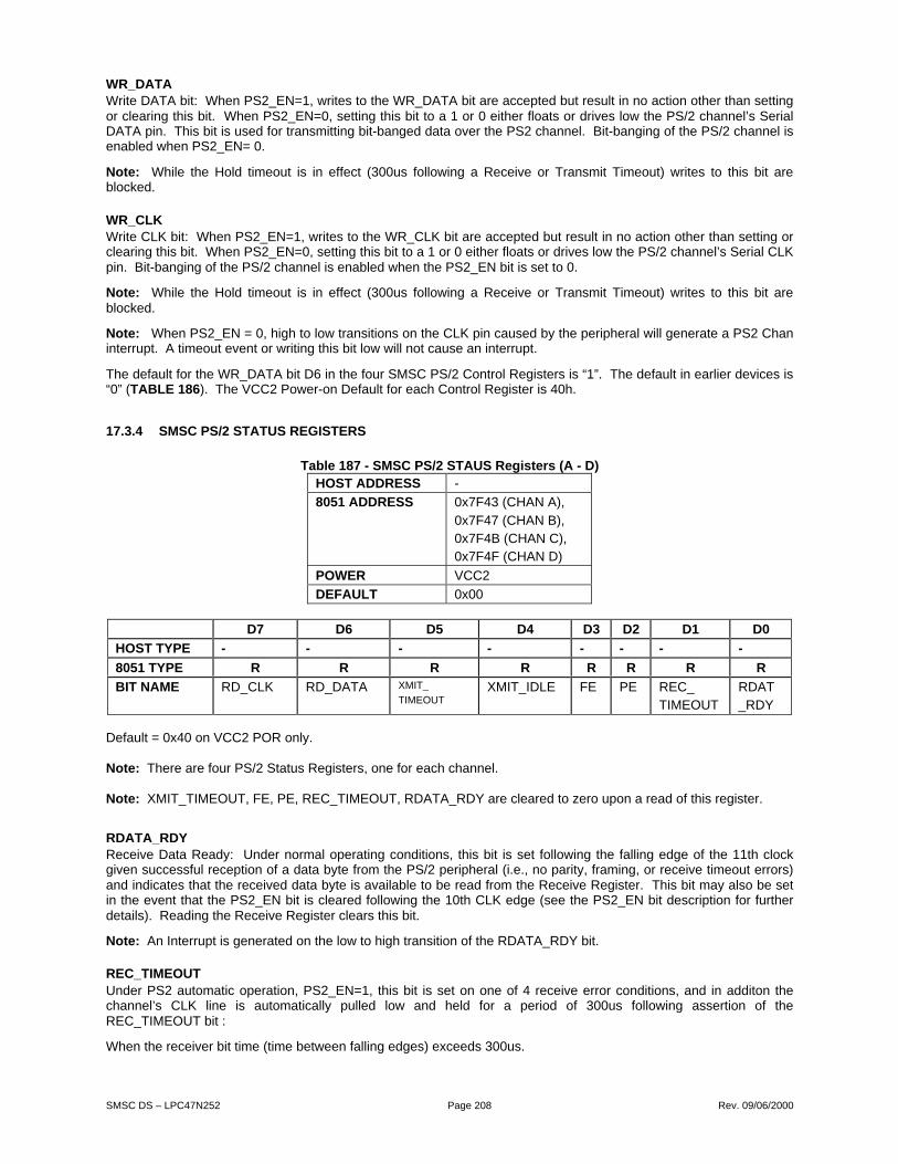
SMSC DS – LPC47N252 Page 208 Rev. 09/06/2000
WR_DATAWrite DATA bit: When PS2_EN=1, writes to the WR_DATA bit are accepted but result in no action other than settingor clearing this bit. When PS2_EN=0, setting this bit to a 1 or 0 either floats or drives low the PS/2 channel’s SerialDATA pin. This bit is used for transmitting bit-banged data over the PS2 channel. Bit-banging of the PS/2 channel isenabled when PS2_EN= 0.
Note: While the Hold timeout is in effect (300us following a Receive or Transmit Timeout) writes to this bit areblocked.
WR_CLKWrite CLK bit: When PS2_EN=1, writes to the WR_CLK bit are accepted but result in no action other than setting orclearing this bit. When PS2_EN=0, setting this bit to a 1 or 0 either floats or drives low the PS/2 channel’s Serial CLKpin. Bit-banging of the PS/2 channel is enabled when the PS2_EN bit is set to 0.
Note: While the Hold timeout is in effect (300us following a Receive or Transmit Timeout) writes to this bit areblocked.
Note: When PS2_EN = 0, high to low transitions on the CLK pin caused by the peripheral will generate a PS2 Chaninterrupt. A timeout event or writing this bit low will not cause an interrupt.
The default for the WR_DATA bit D6 in the four SMSC PS/2 Control Registers is “1”. The default in earlier devices is“0” (TABLE 186). The VCC2 Power-on Default for each Control Register is 40h.
17.3.4 SMSC PS/2 STATUS REGISTERS
Table 187 - SMSC PS/2 STAUS Registers (A - D)HOST ADDRESS -
8051 ADDRESS 0x7F43 (CHAN A),
0x7F47 (CHAN B),0x7F4B (CHAN C),0x7F4F (CHAN D)
POWER VCC2
DEFAULT 0x00
D7 D6 D5 D4 D3 D2 D1 D0
HOST TYPE - - - - - - - -
8051 TYPE R R R R R R R R
BIT NAME RD_CLK RD_DATA XMIT_
TIMEOUTXMIT_IDLE FE PE REC_
TIMEOUTRDAT_RDY
Default = 0x40 on VCC2 POR only.
Note: There are four PS/2 Status Registers, one for each channel.
Note: XMIT_TIMEOUT, FE, PE, REC_TIMEOUT, RDATA_RDY are cleared to zero upon a read of this register.
RDATA_RDYReceive Data Ready: Under normal operating conditions, this bit is set following the falling edge of the 11th clockgiven successful reception of a data byte from the PS/2 peripheral (i.e., no parity, framing, or receive timeout errors)and indicates that the received data byte is available to be read from the Receive Register. This bit may also be setin the event that the PS2_EN bit is cleared following the 10th CLK edge (see the PS2_EN bit description for furtherdetails). Reading the Receive Register clears this bit.
Note: An Interrupt is generated on the low to high transition of the RDATA_RDY bit.
REC_TIMEOUTUnder PS2 automatic operation, PS2_EN=1, this bit is set on one of 4 receive error conditions, and in additon thechannel’s CLK line is automatically pulled low and held for a period of 300us following assertion of theREC_TIMEOUT bit :
When the receiver bit time (time between falling edges) exceeds 300us.
SMSC DS – LPC47N252 Page 209 Rev. 09/06/2000
If the time from the 1st (start) bit to the 10th (parity) bit exceeds 2ms.
On a receive parity error along with the parity error (PE) bit.
On a receive framing error due to an incorrect STOP bit along with the framing error (FE) bit.
The REC_TIMEOUT bit is cleared when the Status Register is read.
Note: An Interrupt is generated on the low to high transition of the REC_TIMEOUT bit.
PEParity Error: When receiving data the parity bit is clocked in on the falling edge of the 10th CLK edge. If the channelhas been set to expect either even or odd parity and the 10th bit is contrary to the expected parity, then the PE andREC_TIMEOUT bits are set following the falling edge of the 10th CLK edge and an Interrupt is generated.
FEFraming Error: When receiving data the stop bit is clocked in on the falling edge of the 11th CLK edge. If thechannel has been set to expect either a high or low stop bit and the 11th bit is contrary to the expected stop polarity,then the FE and REC_TIMEOUT bits are set following the falling edge of the 11th CLK edge and an Interrupt isgenerated.
XMIT_IDLETransmiter Idle: When low, the XMIT_IDLE bit is a status bit indicating that the PS2 channel is actively transmittingdata to the PS2 peripheral device. Writing to the Transmit Register when the channel is ready to transmit will causethe XMIT_IDLE bit to deassert and remain deasserted until one of the following conditions occur:
The falling edge of the 11th CLK; upon a Transmit Timeout condition (XMIT_TIMEOUT goes high);
Upon the PS2_T/R bit being written to 0;
Upon the PS2_EN bit being written to 0.
Note: An interrupt is generated on the low to high transition of XMIT_IDLE.
XMIT_TIMEOUTThis bit is set on one of 3 transmit conditions, and in additon the channel’s CLK line is automatically pulled low andheld for a period of 300us following assertion of the XMIT_TIMEOUT bit during which time the PS2_T/R is also heldlow:
When the transmitter bit time (time between falling edges) exceeds 300us.
When the transmitter start bit is not received withing 25ms from signaling a transmit start event.
If the time from the 1st (start) bit to the 10th (parity) bit exceeds 2ms.
RD_DATARead DATA bit: Reading this bit returns the current level of the PS2 channel’s Serial DATA pin. This bit is used forreceiving bit-banged data over the PS2 channel. Bit-banging of the PS2 channel is enabled when the PS2_EN bit isset to 0. To receive data properly using this bit, PS2_EN must be set to 0 and the WR_DATA bit in the PS2Channel’s Control Register must be set to 1.
RD_CLKRead CLK bit: Reading this bit returns the current level of the PS2 channel’s Serial CLK pin. This bit is used whenreceiving bit-banged data over the PS2 channel. Bit-banging of the PS2 channel is enabled when the PS2_EN bit isset to 0. To receive bit banged data properly the PS2_EN must be set to 0 and the WR_CLK bit in the PS2Channel’s Control Register must be set to 1.
Note: When PS2_EN = 0, high to low transitions on the CLK pin will generate a PS2 Chan interrupt. A timeout eventor writing this bit low will not cause an interrupt.
Note: When PS2_EN=1, bit-banging is disabled for any of the following 3 conditions:Time-out is active.
300us following a time-out (Hold Time).
RDATA_RDY = 1.

SMSC DS – LPC47N252 Page 210 Rev. 09/06/2000
17.3.5 SMSC PS/2 STATUS_2 REGISTERS
The PS/2_STATUS_2 Register supports the RX_Busy indicators for each of the four PS/2 Channels (A - D) When aRX_BUSY bit is set the associated channel is actively receiving PS/2 data; when a RX_BUSY bit is clear the channelis idle.
Table 188 - SMSC PS/2_Status_2 RegisterHOST ADDRESS -
8051 ADDRESS 0x7F48
POWER VCC2
DEFAULT 0x00
D7 D6 D5 D4 D3 D2 D1 D0
HOSTTYPE
- - - - - - - -
8051TYPE
R R R R R R R R
BITNAME
Reserved RX_BUSY D Reserved RX_BUSY C Reserved RX_BUSY B Reserved RX_BUSY A
PROGRAMMER’S NOTE: Always check that an SMSC PS/2 channel is idle, i.e. the RX_BUSY bit is ”0”, beforeattempting to transmit on that channel. Receive data may or may not be lost by setting an SMSC PS/2 channel totransmit while the RX_BUSY bit is asserted depending where in the message frame the tranmit mode change occurs.
17.4 DEVIL LOGIC OVERVIEW
The Devil PS/2 logic allows the host to communicate to any serial auxiliary devices compatible with the PS/2interface through any one of four ports: EM, KB, IM and PS2. There are two identical PS/2 channels, each containinga set of five operating registers. Channel 1 (PS/2 Port 1) consists of ports EM and KB and channel 2 (PS/2 Port 2)consists of ports IM and PS2. The LPC47N252 latches data on the high to low transition of the clock.
17.5 THE DEVIL PS/2 LOGIC COMMANDS
The Devil PS/2 logic supports three commands: Transmit, Receive, and Inhibit.
Notes:
The hardware state machine requires that you read any pending command response byte from the input registerbefore you send an Inhibit command to the device. Since only one response byte is allowed to be automaticallyreceived, there is no need to inhibit the port before you read the response.
After sending a Transmit or Receive command to the Control register, do not read the status register until the PS/2Interrupt Flag is set. If you read the status register to check the BUSY bits, the bit counter will reset and you will eitherget receive time-outs (all bits not received within 2 ms), or you will get parity errors. If there is a receive error, theBUSY bit can be used to determine which device was sending when the error occurred. If there is a transmit error,the ENABLE bit in the Control register can be used to determine which device was selected.
If your PS/2 code is interrupt driven, is best to send the inhibit command while the interrupts are enabled so any bytebeing received can finish and get picked up by the interrupt handler. This is necessary because a receive may havebeen in progress when the Inhibit command was issued, and a receive will complete if the parity bit is reached.
If there is a Request To Send (RTS) time-out or other condition which results in no byte being received from theDEVIL PS/2 device, there will be no device 'data ready' flag set in the status register. It will be necessary to read thedevice enable bits in the status register, or use some other means of tracking.
17.5.1 THE DEVIL PS/2 LOGIC TRANSMIT COMMAND
The Devil PS/2 serial protocol requires that the auxiliary device respond to all transmissions that it receives. Theresponse is usually a 0xFA , 0xFE, 0xFC or 0xEE. The response is stored in the DEVIL PS/2 ports RECEIVEregister. Thus, after each transmission the RECEIVE register should contain some response byte.
SMSC DS – LPC47N252 Page 211 Rev. 09/06/2000
When sending a byte to a DEVIL PS/2 device, Two writes to the control register are required to avoid race conditions:first the device select bit(s) (bits[4:3]) in the control register must be set, clearing the command bits[2:0]; then anotherwrite to the control register selecting ONE command, and preserving the device select bits. The DEVIL PS/2 logicwill assume that the byte being sent is a 'command', and will automatically go into receive mode for a single responsebyte. The DEVIL PS/2 logic must be placed into receive mode to receive additional response bytes. An error will bereported if the device does not start clocking out the command byte within 15 ms, or if the device does not send aresponse within 32 ms of receiving the command. The DEVIL PS/2 logic will cause an interrupt after the responsebyte is received, or if there is a send or receive time-out.
The DEVIL PS/2 logic drives the clock line low and then floats the data line when the port is selected to transmit.Writing to the TRANSMIT register initiates the transmit operation. The data line is driven low and, within 80ns, theclock line is floated (externally pulled high by the pull-up resistor). The auxiliary device recognizes this as the startbit, and responds by providing the eleven clocks (each clock corresponds to a bit). The Logic provides a 3.2µS bithold time. If the auxiliary device did not respond within 15 mS after the start bit, transmit is terminated and ERRORbit of the STATUS register and the RTSTIMOUT bit of the ERROR register are set. The auxiliary device has 2 ms tocomplete the transmission or the DEVIL PS/2 logic will set the ERROR bit of the STATUS register and theXMTTIMOUT bit of the ERROR register. If the transmission is successful, the clock and data lines are floated waitingfor the auxiliary device to send the response packet. If the first byte of the response packet is not received within 32mS, the ERROR bit of the STATUS register is set, the RESTIMOUT bit of the ERROR register is set. If, on the otherhand, the response packet is received and there are no errors, the DEVIL PS/2 logic sets the READY bit of theSTATUS register, clears the ERROR bit of the STATUS register, and clears the ERROR register. The RECEIVEregister contains the received response byte.
17.5.2 THE DEVIL PS/2 LOGIC RECEIVE COMMAND
When receiving scan codes or mouse packets, select one or both DEVIL PS/2 devices in the Control register(bits[4:3]), clearing the command bits[2:0]. Then do another write setting the Receive command bit while preservingthe device select bits. The DEVIL PS/2 logic will only let one device send at a time (whichever starts sending first),and will cause an interrupt for each received byte. Reading the byte from the Receive register causes the DEVILPS/2 logic to go into receive mode again.
The DEVIL PS/2 logic floats the DEVIL PS/2 port’s clock and data line when the port is selected to receive. Theauxiliary device initiates the transfer by driving the data line low and 12µS later driving the clock low. The DEVILPS/2 Logic recognizes this as a start bit and sets the BUSY bit. The auxiliary device proceeds by transmitting tenmore bits to the DEVIL PS/2 logic. The DEVIL PS/2 Logic latches the data on the high to low transition of the clock.After the stop bit, the DEVIL PS/2 Logic clears the BUSY bit and drives the clock line low until the RECEIVE registeris read by the 8051. If there is no error in the transfer, the DEVIL PS/2 logic sets the READY bit of the STATUSregister, clears the ERROR bit of STATUS register, and clears the ERROR register. If, however, the receiveoperation does not complete in 2 ms of receiving a start bit, the ERROR bit of the STATUS register is set togetherwith the RECTIMOUT bit of the ERROR register, and the READY bit is not set.
Note that the logic can be left in receive mode indefinitely and is normally used to receive keyboard scan codes andmouse packets.
17.5.3 THE DEVIL PS/2 LOGIC INHIBIT COMMAND
When you abort a transmission from a DEVIL PS/2 device, it is necessary to hold the clock line low for at least 100 usin order for the device to note that the transmission has been aborted. This 100 us low clock time is called a device'Inhibit'. When you want to perform the Inhibit command, select one or both DEVIL PS/2 devices in the Controlregister, clearing the command bits. Then do another write setting the Inhibit command bit while preserving thedevice select bits. The DEVIL PS/2 logic will hold the device clock lines low and count down 100 us, then it willgenerate an interrupt to indicate that the time-out is over. The interrupt handler should then clear the Inhibitcommand bit in the Control register. After an Inhibit, the device clock lines will remain low until the next Transmit orReceive command.
Note that if the device is receiving a byte when the Inhibit command is sent, and the parity bit has already beenstarted, the device will complete the receipt and set the READY bit before the inhibit takes effect, so it is necessary tocheck for data even when the INHIBIT DONE bit is set.
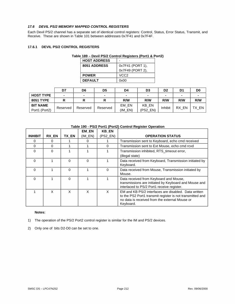
SMSC DS – LPC47N252 Page 212 Rev. 09/06/2000
17.6 DEVIL PS/2 MEMORY MAPPED CONTROL REGISTERS
Each Devil PS/2 channel has a separate set of identical control registers: Control, Status, Error Status, Transmit, andReceive. These are shown in Table 101 between addresses 0x7F41 and 0x7F4F.
17.6.1 DEVIL PS/2 CONTROL REGISTERS
Table 189 – Devil PS/2 Control Registers (Port1 & Port2)HOST ADDRESS -
8051 ADDRESS 0x7F41 (PORT 1),0x7F49 (PORT 2),
POWER VCC2
DEFAULT 0x00
D7 D6 D5 D4 D3 D2 D1 D0
HOST TYPE - - - - - - - -
8051 TYPE R R R R/W R/W R/W R/W R/W
BIT NAMEPort1 (Port2)
Reserved Reserved ReservedEM_EN(IM_EN)
KB_EN(PS2_EN)
Inhibit RX_EN TX_EN
Table 190 - PS/2 Port1 (Port2) Control Register Operation
INHIBIT RX_EN TX_EN
EM_EN
(IM_EN)
KB_EN
(PS2_EN) OPERATION STATUS
0 0 1 0 1 Transmission sent to Keyboard, echo cmd received
0 0 1 1 0 Transmission sent to Ext Mouse, echo cmd rcvd
0 0 1 1 1 Transmission inhibited, RTS_timeout error,(illegal state)
0 1 0 0 1 Data received from Keyboard, Transmission initiated byKeyboard.
0 1 0 1 0 Data received from Mouse, Transmission initiated byMouse.
0 1 0 1 1 Data received from Keyboard and Mouse,transmissions are initiated by Keyboard and Mouse andinterlaced to PS/2 Port1 receive register.
1 X X X X EM and KB PS/2 interfaces are disabled. Data writtento the PS2 Port1 transmit register is not transmitted andno data is received from the external Mouse orKeyboard.
Notes:
1) The operation of the PS/2 Port2 control register is similar for the IM and PS/2 devices.
2) Only one of bits D2-D0 can be set to one.

SMSC DS – LPC47N252 Page 213 Rev. 09/06/2000
17.6.2 DEVIL PS/2 STATUS REGISTERS
Table 191 – Devil PS/2 STATUS Registers (Port1 & Port2)HOST ADDRESS -
8051 ADDRESS 0x7F42 (PORT 1),
0x7F4A (PORT 2),
POWER VCC2
DEFAULT 0x40
D7 D6 D5 D4 D3 D2 D1 D0
HOST TYPE - - - - - - - -
8051 TYPE R R R R R R R R
BIT NAMEPort1 (Port2)
Reserved ReservedEM_busy(IM_busy)
KB_busy(PS2_busy)
Inhibit doneEM_drdy(IM_drdy)
KB_drdy(PS2_drdy)
Error
ErrorThis bit is set in the event of a transmit or receive error condition on either the EM or KB PS/2 ports or the IM or PS/2ports. The cause of the error can be determined by reading the PS/2 Port1 or PS/2 Port2 Status register.
KB_drdyThis bit is set if KB_EN is set and a character has been received successfully from the PS/2 KB port. This bit iscleared when the data has been read from the PS/2 Port1 Receive register.
EM_drdyThis bit is set if EM_EN is set and a character has been received successfully from the PS/2 EM port. This bit iscleared when the data has been read from the PS/2 Port1 Receive register.
PS2_drdyThis bit is set if PS2_EN is set and a character has been received successfully from the PS/2 port. This bit is clearedwhen the data has been read from the PS/2 Port2 Receive register.
IM_drdyThis bit is set if IM_EN is set and a character has been received successfully from the PS/2 IM port. This bit iscleared when the data has been read from the PS/2 Port2 Receive register.
Inhibit doneThis bit is set when the INHIBIT bit of the CONTROL register was set and the 100 uS inhibit sequence has finished.
KB_busyThis bit is set when the PS/2 KB port is actively receiving a character.
EM_busyThis bit is set when the PS/2 EM port is actively receiving a character.
PS2_busyThis bit is set when the PS/2 port is actively receiving a character.
IM_busyThis bit is set when the PS/2 IM port is actively receiving a character.
Note:1) On receive the BUSY bit is set while receiving the first data bit and cleared while receiving the parity bit. On
transmit, the BUSY bit is not set at all.
2) The operation of the PS/2 Port2 status register is similar for the IM and PS/2 devices.

SMSC DS – LPC47N252 Page 214 Rev. 09/06/2000
17.6.3 DEVIL PS/2 ERROR STATUS
Table 192 – Devil PS/2 ERROR STATUS Registers (Port1 & Port2)HOST ADDRESS -
8051 ADDRESS 0x7F43(PORT 1),
0x7F4B(PORT 2),
POWER VCC2
DEFAULT 0x00
D7 D6 D5 D4 D3 D2 D1 D0
HOSTTYPE
- - - - - - - -
8051TYPE
R R R R R R R R
BITNAME
Reserved Reserved Reserved Parity RES_timeout REC_timeout RTS_timeout XMT_timeout
XMT_timeout(Transmit_timeout) is set when the device fails to clock out a command within 2ms of clocking out the start bit.
RTS_timeout(ReadyToSend_timeout) is set when the device fails to start clocking out the command within 15 ms.
REC_timeout(RECeiver_timeout) is set when the device does not finish sending a byte within 2 ms of sending the start bit.
RES_timeout(RESponse_timeout) is set when the response to a command is not received within 32 ms.
ParityThe PS/2 ports use Odd parity, in the event of a receive parity error this bit is set.
17.6.4 DEVIL PS/2 TRANSMIT REGISTERS
Table 193 – Devil PS/2 TRANSMIT Registers (Port1 & port2)HOST ADDRESS -
8051 ADDRESS 0x7F44(PORT 1),
0x7F4C(PORT 2),
POWER VCC2
DEFAULT 0x00
The byte written to the PS/2 Port1(Port2) Transmit register is immediately transmitted onto the enabled PS/2Port1/Port2 provided that the PS/2 Port1(Port2) Inhibit bit is not set and that both PS/2 Port1and Port2 devices arenot enabled for transmit at the same time. This register is write only.

SMSC DS – LPC47N252 Page 215 Rev. 09/06/2000
17.6.5 DEVIL PS/2 RECEIVE REGISTERS
Table 194 – Devil PS/2 RECEIVE Registers (Port1 & Port2)HOST ADDRESS -
8051 ADDRESS 0x7F45(PORT 1),
0x7F4D(PORT 2),
POWER VCC2
DEFAULT 0x00
If KB_EN, and/or EM_EN is set and PS/2 Port1 RX_EN is set any successfully received characters over the KBand/or the EM PS/2 Port are placed into this register and the EM_drdy or KB_drdy PS/2 Port1 status bit is set.Similarly, if PS2_EN and/or IM_EN is set and PS/2 Port2 RX_EN is set any successfully received characters overthe PS2 and/or IM PS2 Ports are placed into this register and the PS2_drdy or IM_drdy PS/2 Port2 status bit is set.

SMSC DS – LPC47N252 Page 216 Rev. 09/06/2000
18 ACCESS.BUS
18.1 OVERVIEW
The LPC47N252 supports ACCESS.Bus. ACCESS.Bus is a serial communication protocol between a computer hostand its peripheral devices. It provides a simple, uniform and inexpensive way to connect peripheral devices to asingle computer port. A single ACCESS.Bus controller on a host can accommodate up to 125 peripheral devices.
The ACCESS.Bus protocol includes a physical layer and several software layers. The software layers include thebase protocol, the device driver interface, and several specific device protocols.
The LPC47N252 implements two ACCESS.Bus controllers (ACCESS.Bus 1 Controller and ACCESS.Bus 2Controller). Each controller, through a multiplexer, can drive two independent sets of Clock and Data pins, as shownin FIGURE 54 - ACCESS.BUS CONTROLLERS.
Four ACCESS.Bus 2 controller pins, AB2A_DATA, AB2A_CLK, AB2B_DATA and AB2B_CLK are multiplexed onGPIO11 through GPIO14. For information regarding multiplexed ACCESS.Bus pins see Table 4 - Alternate FunctionPins on page 15and section 25.5, Multiplexing_3 Register - MISC[23:17] on page 267.
The ACCESS.Bus interface is fully and directly controlled by the on-chip 8051 through its set of on-chip memorymapped control registers. The ACCESS.Bus logic is based on the 8584 Style Physical Layer controller. Addressesfor the registers are shown in Table 195 - ACCESS.Bus Register Address Summary. The ACCESS.Bus logic ispowered on the VCC1 powerplane and clocked by the 8051 clock to provide the ability to wake-up the 8051 on anACCESS.Bus event. When a wakeup event occurs there is a 6 _s max. delay before the ring oscillator starts and anACCESS.Bus event can be detected. This limits the ACCESS,Bus Bus Master Operating Frequency for wakeupevents to 60 KHz. Once the ring oscillator is running the ACCESS,Bus Operating Frequency is a full 100 KHz.
For a description of the ACCESS.Bus protocol, please refer to the ACCESS.Bus Specifications Version 2.2, February1994, available from the ACCESS.Bus Industry Group (ABIG).
I2CCNTLR A
CLK
DATA
AB1A_CLK
AB1B_CLK
AB1A_DATA
AB1B_DATA
I2CCNTLR B
CLK
DATA
AB2A_CLK
AB2B_CLK
AB2A_DATA
AB2B_DATA
SWITCH
SWITCH
I2CA_SEL_A
I2CB_SEL_A
ACCESS.Bus 1
FIGURE 54 - ACCESS.BUS CONTROLLERS
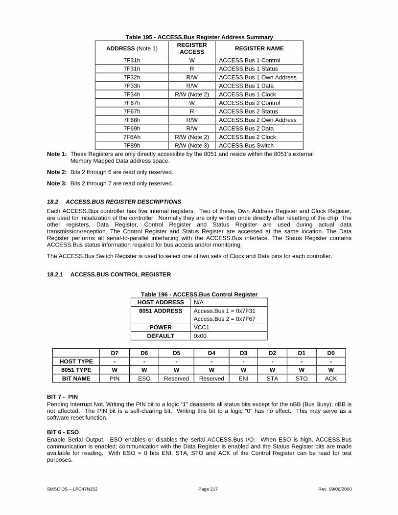
SMSC DS – LPC47N252 Page 217 Rev. 09/06/2000
Table 195 - ACCESS.Bus Register Address Summary
ADDRESS (Note 1)REGISTERACCESS
REGISTER NAME
7F31h W ACCESS.Bus 1 Control
7F31h R ACCESS.Bus 1 Status
7F32h R/W ACCESS.Bus 1 Own Address
7F33h R/W ACCESS.Bus 1 Data
7F34h R/W (Note 2) ACCESS.Bus 1 Clock
7F67h W ACCESS.Bus 2 Control
7F67h R ACCESS.Bus 2 Status
7F68h R/W ACCESS.Bus 2 Own Address
7F69h R/W ACCESS.Bus 2 Data
7F6Ah R/W (Note 2) ACCESS.Bus 2 Clock
7F89h R/W (Note 3) ACCESS.Bus Switch
Note 1: These Registers are only directly accessible by the 8051 and reside within the 8051’s external Memory Mapped Data address space.
Note 2: Bits 2 through 6 are read only reserved.
Note 3: Bits 2 through 7 are read only reserved.
18.2 ACCESS.BUS REGISTER DESCRIPTIONS
Each ACCESS.Bus controller has five internal registers. Two of these, Own Address Register and Clock Register,are used for initialization of the controller. Normally they are only written once directly after resetting of the chip. Theother registers, Data Register, Control Register and Status Register are used during actual datatransmission/reception. The Control Register and Status Register are accessed at the same location. The DataRegister performs all serial-to-parallel interfacing with the ACCESS.Bus interface. The Status Register containsACCESS.Bus status information required for bus access and/or monitoring.
The ACCESS.Bus Switch Register is used to select one of two sets of Clock and Data pins for each controller.
18.2.1 ACCESS.BUS CONTROL REGISTER
Table 196 - ACCESS.Bus Control RegisterHOST ADDRESS N/A
8051 ADDRESS Access.Bus 1 = 0x7F31Access.Bus 2 = 0x7F67
POWER VCC1
DEFAULT 0x00
D7 D6 D5 D4 D3 D2 D1 D0
HOST TYPE - - - - - - - -
8051 TYPE W W W W W W W W
BIT NAME PIN ESO Reserved Reserved ENI STA STO ACK
BIT 7 - PINPending Interrupt Not. Writing the PIN bit to a logic “1” deasserts all status bits except for the nBB (Bus Busy); nBB isnot affected. The PIN bit is a self-clearing bit. Writing this bit to a logic “0” has no effect. This may serve as asoftware reset function.
BIT 6 - ESOEnable Serial Output. ESO enables or disables the serial ACCESS.Bus I/O. When ESO is high, ACCESS.Buscommunication is enabled; communication with the Data Register is enabled and the Status Register bits are madeavailable for reading. With ESO = 0 bits ENI, STA, STO and ACK of the Control Register can be read for testpurposes.
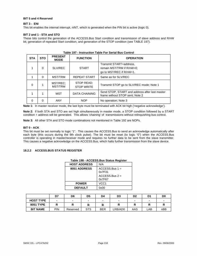
SMSC DS – LPC47N252 Page 218 Rev. 09/06/2000
BIT 5 and 4 Reserved
BIT 3 - ENIThis bit enables the internal interrupt, nINT, which is generated when the PIN bit is active (logic 0).
BIT 2 and 1 - STA and STOThese bits control the generation of the ACCESS.Bus Start condition and transmission of slave address and R/nWbit, generation of repeated Start condition, and generation of the STOP condition (see TABLE 197).
Table 197 - Instruction Table For Serial Bus Control
STA STOPRESENT
MODEFUNCTION OPERATION
1 0 SLV/REC STARTTransmit START+address,remain MST/TRM if R/nW=0;
go to MST/REC if R/nW=1.
1 0 MST/TRM REPEAT START Same as for SLV/REC
0 1MST/REC;MST/TRM
STOP READ;
STOP WRITETransmit STOP go to SLV/REC mode; Note 1
1 1 MST DATA CHAININGSend STOP, START and address after last masterframe without STOP sent; Note 2
0 0 ANY NOP No operation; Note 3
Note 1: In master receiver mode, the last byte must be terminated with ACK bit high (‘negative acknowledge’).
Note 2: If both STA and STO are set high simultaneously in master mode, a STOP condition followed by a STARTcondition + address will be generated. This allows ‘chaining’ of transmissions without relinquishing bus control.
Note 3: All other STA and STO mode combinations not mentioned in Table 192 are NOPs.
BIT 0 - ACKThis bit must be set normally to logic “1”. This causes the ACCESS.Bus to send an acknowledge automatically aftereach byte (this occurs during the 9th clock pulse). The bit must be reset (to logic “0”) when the ACCESS.Buscontroller is operating in master/receiver mode and requires no further data to be sent from the slave transmitter.This causes a negative acknowledge on the ACCESS.Bus, which halts further transmission from the slave device.
18.2.2 ACCESS.BUS STATUS REGISTER
Table 198 - ACCESS.Bus Status RegisterHOST ADDRESS N/A
8051 ADDRESS ACCESS.Bus 1 =0x7F31ACCESS.Bus 2 =0x7F67
POWER VCC1
DEFAULT 0x00
D7 D6 D5 D4 D3 D2 D1 D0
HOST TYPE - - - - - - - -
8051 TYPE R R R R R R R R
BIT NAME PIN Reserved STS BER LRB/AD0 AAS LAB nBB

SMSC DS – LPC47N252 Page 219 Rev. 09/06/2000
BIT 7 - PINPending Interrupt Not. This bit is a status flag which is used to synchronize serial communication and is set to logic“0” whenever the chip requires servicing. The PIN bit is normally read in polled applications to determine when anACCESS.Bus byte transmission/reception is completed.
When acting as transmitter, PIN is set to logic “1” (inactive) each time the Data Register is written. In receiver mode,the PIN bit is automatically set to logic “1” each time the Data Register is read.
After transmission or reception of one byte on the ACCESS.Bus (nine clock pulses, including acknowledge) the PINbit will be automatically reset to logic “0” (active) indicating a complete byte transmission/reception. When the PIN bitis subsequently set to logic “1” (inactive) all status bits will be reset to “0” on a BER (bus error) condition.
In polled applications, the PIN bit is tested to determine when a serial transmission/reception has been completed.When the ENI bit (bit 3 of the Control Register) is also set to logic “1” the hardware interrupt is enabled. In this case,the PI flag also triggers and internal interrupt (active low) via the nINT output each time PIN is reset to logic “0”.
When acting as a slave transmitter or slave receiver, while PIN = “0”, the chip will suspend ACCESS.Bustransmission by holding the SCL line low until the PIN bit is set to logic “1” (inactive). This prevents further data frombeing transmitted or received until the current data byte in the Data Register has been read (when acting as slavereceiver) or the next data byte is written to the Data Register (when acting as slave transmitter).
PIN Bit Summary:
The PIN bit can be used in polled applications to test when a serial transmission has been completed. When the ENIbit is also set, the PIN flag sets the internal interrupt via the nINT output.
In transmitter mode, after successful transmission of one byte on the ACCESS.Bus the PIN bit will be automaticallyreset to logic “0” (active) indicating a complete byte transmission.
In transmitter mode, PIN is set to logic “1” (inactive) each time the Data Register is written.
In receiver mode, PIN is set to logic “0” (inactive) on completion of each received byte. Subsequently, the SCL linewill be held low until PIN is set to logic “1”.
In receiver mode, when the Data Register is read, PIN is set to logic “1” (inactive).
In slave receiver mode, an ACCESS.Bus STOP condition will set PIN=0 (active).
PIN=0 if a bus error (BER) occurs.
BIT 6 - Reserved (Read returns 0)
BIT 5 - STSWhen in slave receiver mode, this flag is asserted when an externally generated STOP condition is detected (usedonly in slave receiver mode).
BIT 4 - BERBus error; a misplaced START or STOP condition has been detected. Resets nBB (to logic “1”; inactive), sets PIN =“0” (active).
BIT 3 - LRB/AD0Last Received Bit or Address 0 (general call) bit. This status bit serves a dual function, and is valid only while PIN=0.
LRB holds the value of the last received bit over the ACCESS.Bus while AAS=0 (not addressed as slave). Normallythis will be the value of the slave acknowledgment; thus checking for slave acknowledgment is done via testing of theLRB.
When AAS = 1 (Addressed as slave condition) the ACCESS.Bus controller has been addressed as a slave. Underthis condition, this bit becomes the AD0 bit and will be set to logic “1” if the slave address received was the ‘generalcall’ (00h) address, or logic “0” if it was the ACCESS.Bus controller’s own slave address.
BIT 2 - AASAddressed As Slave bit. Valid only when PIN=0. When acting as slave receiver, this flag is set when an incomingaddress over the ACCESS.Bus matches the value in own address register S0’ (shifted by one bit) or if theACCESS.Bus ‘general call’ address (00h) has been received (‘general call’ is indicated when AD0 status bit is alsoset to logic “1”).

SMSC DS – LPC47N252 Page 220 Rev. 09/06/2000
BIT 1 - LABLost Arbitration Bit. This bit is set when, in multi-master operation, arbitration is lost to another master on theACCESS.Bus.
BIT 0 - nBBBus Busy bit. This is a read-only flag indicating when the ACCESS.Bus is in use. A zero indicates that the bus isbusy, and access is not possible. This bit is set/reset (logic “1”/logic “0”) by Stop/Start conditions.
18.2.3 OWN ADDRESS REGISTER
When the chip is addressed as slave, this register must be loaded with the 7-bit ACCESS.Bus address to which thechip is to respond. During initialization, the Own Address Register must be written to, regardless whether it is laterused. The Addressed As Slave (AAS) bit in the Status Register is set when this address is received (the value in theData Register is compared with the value in the Own Address Register). Note that the Data Register and OwnAddress Register are offset by one bit; hence, programming the Own Address Register with a value of 55h will resultin the value AAh being recognized as the chip’s ACCESS.Bus slave address.
After reset, the Own Address Register has default address 00h.
Table 199 – Own Address RegisterHOST ADDRESS N/A
8051 ADDRESS ACCESS.Bus 1 = 0x7F32ACCESS.Bus 2 = 0x7F68
POWER VCC1
DEFAULT 0x00
D7 D6 D5 D4 D3 D2 D1 D0
HOST TYPE - - - - - - - -
8051 TYPE R/W R/W R/W R/W R/W R/W R/W R/W
BIT NAME ReservedSlave
Address 6Slave
Address 5Slave
Address 4Slave
Address 3Slave
Address 2Slave
Address 1Slave
Address 0
18.2.4 DATA REGISTER
The Data Register acts as serial shift register and read buffer interfacing to the ACCESS.Bus. All read and writeoperations to/from the ACCESS.Bus are done via this register. ACCESS.Bus data is always shifted in or out of theData Register.
In receiver mode the ACCESS.Bus data is shifted into the shift register until the acknowledge phase. Furtherreception of data is inhibited (SCL held low) until the Data Register is read.
In the transmitter mode data is transmitted to the ACCESS.Bus as soon as it is written to the Data Register if theserial I/O is enabled (ESO=1).
Table 200 – Data RegisterHOST ADDRESS N/A
8051 ADDRESS ACCESS.Bus 1 = 0x7F33ACCESS.Bus 2 = 0x7F69
POWER VCC1
DEFAULT 0x00
D7 D6 D5 D4 D3 D2 D1 D0
HOST TYPE - - - - - - - -
8051 TYPE R/W R/W R/W R/W R/W R/W R/W R/W
BIT NAME Data Bit 7 Data Bit 6 Data Bit 5 Data Bit 4 Data Bit 3 Data Bit 2 Data Bit 1 Data Bit 0

SMSC DS – LPC47N252 Page 221 Rev. 09/06/2000
18.2.5 CLOCK REGISTER
The Clock Register controls selection of the internal chip clock frequency used for the ACCESS.Bus block. Thisdetermines the SCL clock frequency generated by the chip. The selection is made via Bits[2:0].
Table 201 – Clock RegisterHOST ADDRESS N/A
8051 ADDRESS ACCESS.Bus 1 = 0x7F34
ACCESS.Bus 2 = 0x7F6A
POWER VCC1
DEFAULT 0x00
D7 D6 D5 D4 D3 D2 D1 D0
HOST TYPE - - - - - - - -
8051 TYPE R/W R R R R R/W R/W R/W
BIT NAME AB_RST Reserved Reserved Reserved Reserved CLK_DIV
CLOCK SELECT
00 = Clock Off01 = Reserved
10 = 8051 Clock11 = 24 MHz. Clock
BIT 7 – AB_RSTACCESS.Bus Reset. Setting this bit re-initializes all logic and registers in the ACCESS.Bus block. AB_RST is notself-clearing. It must be written high and then written low.
BITS 6 through 3 – Reserved (Reads return 0)
BIT 2 - CLK_DIVClock Divider Bit. The clock divider bit CLK_DIV affects all ACCESS.Bus clock inputs. When CLK_DIV is “1”, theACCESS.Bus input clock is divided by 2. When CLK_DIV is “0”, the ACCESS.bus input clock is not divided.
BITS 1 and 0 – CLOCK SELECTClock Selection Bits. These bits determine the source of the clock used by the ACCESS.Bus Controller. Encoding ofthese bits are as shown in Table 201 – Clock Register, above. Data rates produced by the selected clock are shownin Table 202 - Internal Clock Rates and ACCESS.Bus Data Rates, below.
Table 202 - Internal Clock Rates and ACCESS.Bus Data Rates
CLOCK SELECTCLOCK RATE
DATA RATE(f/240)
NOMINALHIGH(96/f)
NOMINALLOW(144/f)
MINIMUMHIGH
(18/f) Note 1
00 Off - - - -
01 n/a - - - -
Ring Osc=4 MHz 16.7 KHz 24 µs 36 µs 4.5 µs
Ring Osc=6 MHz 25 KHz 16 µs 24 µs 3 µs
Ring Osc=8 MHz 33.3 KHz 12 µs 18 µs 2.25 µs
12 MHz 50 KHz 8 µs 12 µs 4 µs
16 MHz 67 KHz 6 µs 9 µs 4 µs
24 MHz 100 KHz 4 µs 6 µs 4 µs
10(8051 ClockSelection)
32 MHz 133 KHz 3 µs 4.5 µs TBD
Eng Note 1
11 24 MHz 100 KHz 4 µs 6 µs 4 µs
f = frequency of the ring oscillator.
Note 1: 18/f pertains to Ring Osc rates only.

SMSC DS – LPC47N252 Page 222 Rev. 09/06/2000
18.2.6 ACCESS.BUS SWITCH REGISTER
The ACCESS.Bus Switch register is used to control the ACCESS.bus Multiplexer. Each of the two ACCESS.buscontrollers in the LPC47N252 can drive two independent sets of Clock and Data pins (FIGURE 54). The selectedClock and Data pins for each ACCESS.Bus controller are determined by the ACCESS.BusA_SEL_A andACCESS.BusB_SEL_A bits, D1 and D0 respectively, in the ACCESS.Bus Switch register.
Table 203 - ACCESS.Bus Switch RegisterHOST ADDRESS N/A
8051 ADDRESS 0x7F89
POWER VCC1
DEFAULT 0x03
D7 D6 D5 D4 D3 D2 D1 D0
HOST TYPE - - - - - - - -
8051 TYPE R R R R R R R/W R/W
BIT NAME RESERVED ACCESS.BusB_SEL_A
ACCESS.BusA_SEL_A
BITS 7 through 2 – Reserved (Reads return 0)
BIT 1 - ACCESS.BUSB_SEL_AThe ACCESS.BusB_SEL_A bit determines the selected Clock and Data pins for the ACCESS.Bus 2 controller(FIGURE 54). When the ACCESS.BusB_SEL_A bit is ‘1’ (default), the AB2A_CLOCK and AB2A_DATA pins aredriven by the ACCESS.Bus B controller. The AB2B_CLOCK and AB2B_DATA pins are tristated. When theACCESS.BusB_SEL_A bit is ‘0’, the AB2B_CLOCK and AB2B_DATA pins are driven by the ACCESS.Bus 2controller. The AB2A_CLOCK and AB2A_DATA pins are tristated.
BIT 0 - ACCESS.BUSA_SEL_AThe ACCESS.BusA_SEL_A bit determines the selected Clock and Data pins for the ACCESS.Bus 1 controller(FIGURE 54). When the ACCESS.BusA_SEL_A bit is ‘1’ (default), the AB1A_CLOCK and AB1A_DATA pins aredriven by the ACCESS.Bus 1 controller. The AB1B_CLOCK and AB1B_DATA pins are tristated. When theACCESS.BusA_SEL_A bit is ‘0’, the AB1B_CLOCK and AB1B_DATA pins are driven by the ACCESS.Bus 1controller. The AB1A_CLOCK and AB1A_DATA pins are tristated.

SMSC DS – LPC47N252 Page 223 Rev. 09/06/2000
19 MAILBOX REGISTER INTERFACE
19.1 OVERVIEW
The Mailbox Registers Interface provides a standard run-time mechanism for the host to communicate with the 8051and other logical components in the LPC47N252. The Mailbox Registers Interface includes a total of 48 index-addressable 8-bit registers (Table 204) and two 8-bit host access ports (Table 206). Thirty-two of these 48 registersare 8051 Mailbox registers.
The Mailbox Registers Interface host access ports are run-time registers that occupy two addresses in the system I/Ospace. The access ports are used by the host to read and write the 48 registers. The access ports base address isdetermined by the Mailbox Registers Interface Base Address that is initialized in Logical Device Number 9 inLPC47N252 configuration registers CR60 and CR61 (Table 205).
The 32 Mailbox registers as well as the PWM0, PWM1, Fan Control registers, Flash Program Register, and FlashHigh Address are directly addressable by the 8051 through Memory-Mapped Control Registers (see Table 101 - 8051On-Chip External Memory Mapped Registers on page 128).
In this specification, the registers in the Mailbox Registers Interface are identified by the prefix MBX in front of ahexadecimal index address. Table 204 below summarizes the 48 registers in the Mailbox Registers Interface.
Table 204 – Mailbox Registers Interface
REGISTER NAME
MAILBOXINDEX
ADDRESSSYSTEM
R/W
8051ADDR.(7F00+)
8051R/W
POWERPLANE
VCC1POR
VCC2POR NOTES
Flash Low Address MBX80h R/W B1h R/W VCC1 00h -
Flash Data MBX81h R/W B2h R/W VCC1 00h -
System-to-8051Mailbox register 0-
MBX82h R/W 08h RC VCC1 00h -
8051-to-system
Mailbox register 1
MBX83h RC 09h R/W VCC1 00 Note 54
Mailbox register [2-F] MBX 84h-91h
R/W 0Ah –17h
R/W VCC1 00h Note 55
PWM0 register MBX92h R/W 25h R/W VCC1 00h
PWM1 register MBX93h R/W 26h R/W VCC1 00h
8051STP_CLK MBX94h R/W - - VCC1 00h
PWM2 register MBX95h R/W 29h R/W VCC2 00h
ESMI source register MBX96h R/W - - VCC2 00h
ESMI mask register MBX97h R/W - - VCC2 00h
IR data register MBX98h R/W - - VCC2 00h
Force Disk Changeregister
MBX99h R/W - - VCC2 03h
Floppy Data RateSelect Shadow register
MBX9Ah R - - VCC2 N/A
UART1 FIFO ControlShadow register
MBX9Bh R - - VCC2 00h
Reserved MBX9Ch R - - VCC2 00h Note 56
Fan Control Register MBX9Dh R/W 28h R/W VCC1 0x30 -
Flash Program Register MBX9Eh R/W 35h R/W VCC1 -
Flash High Address MBX9Fh R/W B0h R/W VCC1 00h -
Mailbox Register [10-1F]
MBXA0h-AFh
R/W 70h –7Fh
R/W VCC1 00h -

SMSC DS – LPC47N252 Page 224 Rev. 09/06/2000
Note 54: Interrupt is cleared when read by the 8051.
Note 55: Interrupt is cleared when read by the host.
Note 56: This register is reserved and should not be accessed.
19.2 MAILBOX REGISTERS INTERFACE BASE ADDRESS
Logical Device 9 in the LPC47N252 configuration space supports the Mailbox Registers Interface. The three deviceconfiguration registers in LDN9 provide activation control and the base address for the Mailbox Registers Interfacerun-time registers (Table 205).
Register 0x30 is the Activate register. The activation control (LDN9:CR30.0) qualifies address decoding for theMailbox Registers Interface; e.g., if the Activate bit D0 in the Activate register is “0”, the MBX access port addresseswill not be decoded; if the Activate bit is “1”, MBX access port addresses will be decoded depending on the valuesprogrammed in the MBX Primary Base Address registers.
Registers 0x60 and 0x61 are the MBX Primary Base Address registers. Register 0x60 is the MBX Primary BaseAddress High Byte, register 0x61 is the MBX Primary Base Address Low Byte.
Note: Bit D0 in the MBX Primary Base Address Low Byte must be “0”. Valid Mailbox Registers Interface BaseAddress values are 0x0000 – 0x0FFE.
Table 205 – Mailbox Registers Interface Configuration Controls (LDN9)
INDEX TYPEHARDRESET
SOFTRESET
VCC2POR
VCC1 &VCC0POR DESCRIPTION
D7 D6 D5 D4 D3 D2 D1 D0
0x30 R/W 0x00 0x00 0x00 - Activate
RESERVED Activate
0x60 R/W 0x00 0x00 0x00 - MBX Primary Base Address High Byte
“0” “0” “0” “0” A11 A10 A9 A8
0x61 R/W 0x00 0x00 0x00 - MBX Primary Base Address Low Byte
A7 A6 A5 A4 A3 A2 A1 “0”
19.3 MAILBOX REGISTERS INTERFACE ACCESS PORTS
The Mailbox registers access ports are runtime registers that occupy two addresses in the Host I/O space (Table206).
To access a Mailbox register once the Mailbox Registers Interface Base Address has been initialized, write theMailbox register index address to the MBX Index port and read or write the Mailbox register data from the MBX dataport.
Table 206 – Mailbox Registers Interface Access PortsACCESS
PORT NAME HOST ADDRESS
HOSTTYPE
POWER
PLANE
VCC2POR
VCC1POR
MBX INDEX MBX Base Address R/W VCC2 0x00 -
MBX DATA MBX Base Address + 1 R/W VCC2 - -
19.4 MAILBOX REGISTERS
There are 32 Mailbox Registers in the LPC47N252. The MBXA0–AF and MBX84– 91 Mailbox Registers are generalpurpose registers. There are no interrupts for these registers.

SMSC DS – LPC47N252 Page 225 Rev. 09/06/2000
19.5 THE SYSTEM/8051 INTERFACE REGISTERS
Mailbox Register 0, System-to-8051, and Mailbox Register 1, 8051-to-System, are specifically designed to passcommands between the host and the 8051 (FIGURE 55). If enabled, these registers can generate interrupts.
Mailbox Register 0 and Mailbox Register 1 are not dual-ported, so the System BIOS and Keyboard BIOS must bedesigned to properly share these registers. When the host performs a write of the System-to-8051 mailbox register,an 8051 INT1 will be generated and seen by the 8051 if unmasked. When the 8051 writes to the System-to-8051mailbox register, the data is blocked but the write forces the register to 0x00, providing a simple means for the 8051to inform that host that an operation has been completed.
When the 8051 writes the 8051-to-System mailbox register, an SMI may be generated and seen by the host ifunmasked. When the Host CPU writes to the 8051-to-System mailbox register, the data is blocked but the writeforces the 8051-to-System register to clear to zero, providing a simple means for the host to inform that 8051 that anoperation has been completed.
PROGRAMMER’S NOTE: The protocol used to pass commands back and forth through the Mailbox RegistersInterface is left to the system designer. SMSC can provide an application example of working code in which the hostuses the Mailbox registers to gain access to all of the 8051 registers.
32 8-bitMail-BoxRegisters
HOST CPU 8051
8051-to-System
System-to-8051
SMI INT1
FIGURE 55 – SYSTEM-TO-8051 MAILBOX INTERFACE REGISTERS BLOCK DIAGRAM
19.5.1 MAILBOX REGISTER 0: SYSTEM-TO-8051
If enabled, an INT1 will be generated when the System writes to Mailbox Register 0 (Table 207). The interruptsource bit will be cleared when the 8051 reads this register.
After reading Mailbox Register 0, the 8051 can clear the register to “00H” by a dummy write to inform the host that theregister contents have been read.
Table 207 – Mailbox Register 0 (System-To-8051)MAILBOX INDEX 8051 ADDRESS POWER PLANE DEFAULT
0x82 0x7F08 VCC1 0x00
D7 D6 D5 D4 D3 D2 D1 D0
MBX TYPE1 RC RC RC RC RC RC RC RC
8051 TYPE R/W R/W R/W R/W R/W R/W R/W R/W
BIT NAME D7 D6 D5 D4 D3 D2 D1 D0
Note1 RC = Read-only register is cleared when written.
Mailbox Register 1: 8051-to-system
If enabled, an SMI will be generated when the 8051 writes to Mailbox Register 1 (Table 205). The SMI interrupt willbe cleared when the host reads this register.

SMSC DS – LPC47N252 Page 226 Rev. 09/06/2000
After reading Mailbox Register 1, the system can clear the register to “00H” by a dummy write to inform the 8051 thatthe register has been read.
Table 208 – Mailbox Register 1 (8051-To-System)MAILBOX INDEX 8051 ADDRESS POWER PLANE DEFAULT
0x83 0x7F09 VCC1 0x00
D7 D6 D5 D4 D3 D2 D1 D0
MBX TYPE1 RC RC RC RC RC RC RC RC
8051 TYPE R/W R/W R/W R/W R/W R/W R/W R/W
BIT NAME D7 D6 D5 D4 D3 D2 D1 D0
Note1 RC = Read-only register is cleared when written.
19.6 8051 STOP CLOCK REGISTER
The LPC Host can use the STP_CLK bit to stop the 8051 clock, for example when the LPC Bus Flash ProgramAccess interface is used to update the 64k Embedded Flash.
FIGURE 56 illustrates the sequence the LPC Host must follow to stop the 8051 clock. The - 8051 STP_CLK Registershown in Table 209 contains the STP_CLK bit.

SMSC DS – LPC47N252 Page 227 Rev. 09/06/2000
8051goes into idle mode
YN
System is fully powered & the8051is running keyboard code:nRESET_OUT = 1, STP_CLK = 0
The host issues a definedcommand to put the 8051 intoIdle mode
The host sets STP_CLK = 1and combined withnRESET_OUT=1 causes the8051 clock to stop
The host can operate asneeded.
When done, the host resetsSTP_CLK = 0
8051 IRQ?(note) 8051 wakes from idle mode
and starts from where it left off
NOTE: in order to leave idle mode the 8051 must receive an interrupt;typically a software timer interrupt will be used
FIGURE 56 - LPC HOST SEQUENCE TO STOP THE 8051
Table 209 - 8051 STP_CLK RegisterHOST ADDRESS MBX94h
8051 ADDRESS N/A
POWER VCC1
DEFAULT 0x00
D7 D6 D5 D4 D3 D2 D1 D0
HOST TYPE - - - - - - - -
8051 TYPE R R R R R R R R/W
BIT NAME IDLE RESERVED STP_CLK
IDLE Bit – D7When the IDLE bit is ‘0’, the 8051 is not in idle mode; when the IDLE bit is ‘1’, the 8051 is in idle mode. The IDLE bitis read-only.

SMSC DS – LPC47N252 Page 228 Rev. 09/06/2000
STP_CLK Bit – D0When the STP_CLK bit is ‘1’, the 8051 clock is stopped only when the nRESET_OUT pin is deasserted; when theSTP_CLK bit is ‘0’, the 8051 clock can run. The STP_CLK bit is read/write. See section 11.8.3.5, Output EnableRegister on page 134.
19.7 ESMI REGISTERS
The host can enable/disable the SMI interrupts generated as a result of the 8051 writing to Mailbox register 1. Thehost can read the ESMI source register to determine fo the LPC47N252 Mailbox interface was the cause of the SMI.
Table 210 – ESMI Source RegisterHOST ADDRESS MBX96
8051 ADDRESS N/A
POWER VCC2
DEFAULT 0x00
D7 D6 D5 D4 D3 D2 D1 D0
HOST TYPE - - - - - - - -
8051 TYPE R R R R R/W R/ R/ R/
BIT NAME Reserved Reserved Reserved Reserved 8051_WR Reserved Reserved Reserved
8051_WRThis bit is set when a 8051-to-host mailbox has been written . This bit is cleared by a read of Mailbox Register 1(MBX83.)
Table 211 – ESMI Mask RegisterHOST ADDRESS MBX97
8051 ADDRESS N/A
POWER VCC2
DEFAULT 0x00
D7 D6 D5 D4 D3 D2 D1 D0
HOST TYPE - - - - - - - -
8051 TYPE R R R R R/W R R R
BIT NAME Reserved Reserved Reserved Reserved ESMI_MASK Reserved Reserved Reserved
ESMI_MASKSetting this bit masks the 8051-to-host mailbox SMI.
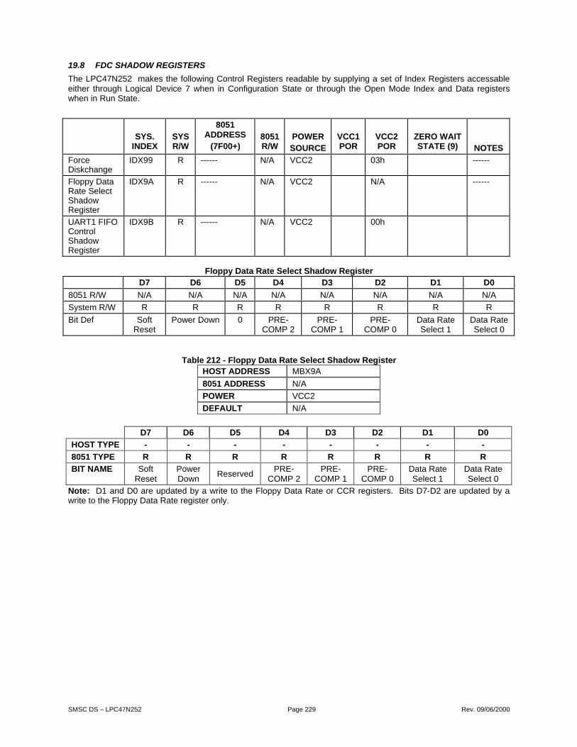
SMSC DS – LPC47N252 Page 229 Rev. 09/06/2000
19.8 FDC SHADOW REGISTERS
The LPC47N252 makes the following Control Registers readable by supplying a set of Index Registers accessableeither through Logical Device 7 when in Configuration State or through the Open Mode Index and Data registerswhen in Run State.
SYS.INDEX
SYSR/W
8051ADDRESS
(7F00+)8051R/W
POWERSOURCE
VCC1POR
VCC2POR
ZERO WAITSTATE (9) NOTES
ForceDiskchange
IDX99 R ------ N/A VCC2 03h ------
Floppy DataRate SelectShadowRegister
IDX9A R ------ N/A VCC2 N/A ------
UART1 FIFOControlShadowRegister
IDX9B R ------ N/A VCC2 00h
Floppy Data Rate Select Shadow RegisterD7 D6 D5 D4 D3 D2 D1 D0
8051 R/W N/A N/A N/A N/A N/A N/A N/A N/A
System R/W R R R R R R R R
Bit Def SoftReset
Power Down 0 PRE-COMP 2
PRE-COMP 1
PRE-COMP 0
Data RateSelect 1
Data RateSelect 0
Table 212 - Floppy Data Rate Select Shadow RegisterHOST ADDRESS MBX9A
8051 ADDRESS N/A
POWER VCC2
DEFAULT N/A
D7 D6 D5 D4 D3 D2 D1 D0
HOST TYPE - - - - - - - -
8051 TYPE R R R R R R R R
BIT NAME SoftReset
PowerDown
ReservedPRE-
COMP 2PRE-
COMP 1PRE-
COMP 0Data RateSelect 1
Data RateSelect 0
Note: D1 and D0 are updated by a write to the Floppy Data Rate or CCR registers. Bits D7-D2 are updated by awrite to the Floppy Data Rate register only.

SMSC DS – LPC47N252 Page 230 Rev. 09/06/2000
Table 213 - Forced Disk Change RegisterHOST ADDRESS MBX99
8051 ADDRESS N/A
POWER VCC2
DEFAULT 0x03
D7 D6 D5 D4 D3 D2 D1 D0
HOST TYPE - - - - - - - -
8051 TYPE R R R R R R R/W R/W
BIT NAMEReserved Reserved Reserved Reserved Reserved Reserved
ForcedDSK_CHG 1
ForcedDSK_CHG 0
These bits can be written to a “1” but are not clearable by the software. These bits are reset when nSTEP input isactive with the proper drive select to the drive occurs. D0 is cleared on nSTEP and Drive Select 0; D1 is cleared onnSTEP and Drive Select 1. A Force diskchange indication is read in the DIR register (of the Floppy controller) andgated with Drive Select 0 or 1.
The Equivalent logic: when read DIR bit 7 = (Drive_Sel_0 & D0) OR (Drive_Sel_1 & D1) OR DSK_CHG.DSK_CHG is the inverse of the nDSKCHG signal.
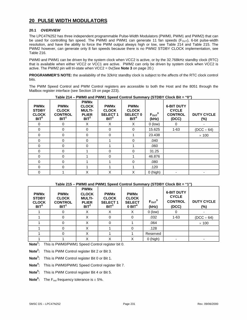
SMSC DS – LPC47N252 Page 231 Rev. 09/06/2000
20 PULSE WIDTH MODULATORS
20.1 OVERVIEW
The LPC47N252 has three independent programmable Pulse-Width Modulators (PWM0, PWM1 and PWM2) that canbe used for controlling fan speed. The PWM0 and PWM1 can generate 11 fan speeds (FOUT), 6-bit pulse-widthresolution, and have the ability to force the PWM output always high or low, see Table 214 and Table 215. ThePWM2 however, can generate only 8 fan speeds because there is no PWM2 STDBY CLOCK implementation, seeTable 216.
PWM0 and PWM1 can be driven by the system clock when VCC2 is active, or by the 32.768kHz standby clock (RTC)that is available when either VCC2 or VCC1 are active. PWM2 can only be driven by system clock when VCC2 isactive. The PWM2 pin will tri-state when VCC2 = 0v(See Note 3 on page 20.)
PROGRAMMER’S NOTE: the availability of the 32kHz standby clock is subject to the affects of the RTC clock controlbits.
The PWM Speed Control and PWM Control registers are accessible to both the Host and the 8051 through theMailbox register interface (see Section 19 on page 223).
Table 214 – PWM0 and PWM1 Speed Control Summary (STDBY Clock Bit = “0”)
PWMxSTDBYCLOCK
BIT5
PWMxCLOCK
CONTROLBIT1
PWMxCLOCKMULTI-PLIERBIT2
PWMxCLOCK
SELECT 1BIT3
PWMxCLOCK
SELECT 0BIT4
FOUT6
(kHz)
6-BIT DUTYCYCLE
CONTROL(DCC)
DUTY CYCLE(%)
0 0 X X X 0 (low) 0 -
0 0 0 0 0 15.625 1-63 (DCC ÷ 64)
0 0 0 0 1 23.438 × 100
0 0 0 1 0 .040
0 0 0 1 1 .060
0 0 1 0 0 31.25
0 0 1 0 1 46.876
0 0 1 1 0 .080
0 0 1 1 1 .120
0 1 X X X 0 (high) - -
Table 215 – PWM0 and PWM1 Speed Control Summary (STDBY Clock Bit = “1”)
PWMxSTDBYCLOCK
BIT5
PWMxCLOCK
CONTROLBIT1
PWMx
CLOCKMULTI-PLIERBIT2
PWMxCLOCK
SELECT 1BIT3
PWMxCLOCKSELECT0 BIT4
FOUT6
(kHz)
6-BIT DUTYCYCLE
CONTROL
(DCC)
DUTY CYCLE
(%)
1 0 X X X 0 (low) 0 -
1 0 X 0 0 .032 1-63 (DCC ÷ 64)
1 0 X 0 1 .064 × 100
1 0 X 1 0 .128
1 0 X 1 1 Reserved
1 1 X X X 0 (high) - -
Note1: This is PWM0/PWM1 Speed Control register bit 0.
Note2: This is PWM Control register Bit 2 or Bit 3.
Note3: This is PWM Control register Bit 0 or Bit 1.
Note4: This is PWM0/PWM1 Speed Control register Bit 7.
Note5: This is PWM Control register Bit 4 or Bit 5.
Note6: The Fout frequency tolerance is ± 5%.

SMSC DS – LPC47N252 Page 232 Rev. 09/06/2000
Table 216 - PWM2 Speed Control Summary
PWM2CLOCK
CONTROLBIT1
PWM2CLOCK
SELECT 1BIT3
PWM2CLOCKMULTI-PLIERBIT2
PWM2CLOCK
SELECT 0BIT4
FOUT5
(kHz)
6-BITDUTY
CYCLECONTROL
(DCC)
DUTYCYCLE
(%)
0 X X X 0 (low) 0 -
0 0 0 0 15.625
0 0 0 1 23.438
0 0 1 0 31.25
0 0 1 1 46.876
0 1 0 0 0.1831
0 1 0 1 0.275
0 1 1 0 0.36666
0 1 1 1 0.550
1-63 (DCC ÷ 64)
× 100
1 X X X 0 (high) - -
Note1: This is PWM2 Speed Control register bit 0.
Note2: This is PWM Control register Bit 7.
Note3: This is PWM Control register Bit 6.
Note4: This is PWM2 Speed Control register Bit 7.
Note5: For Fout = 275Hz, i.e. when the PWM2 Clock Control Bit = ‘0’, Clock Select 0 = Clock Select 1 = ‘1’, and theClock Multiplier Bit = ‘0’, the frequency tolerance is ± 10 Hz, otherwise the Fout frequency tolerance is ± 5%.
20.2 PWM SPEED CONTROL REGISTERS
There are three PWM Speed Control registers: PWM0, PWM1 and PWM2. These registers are located in theLPC47N252 Mailbox Registers Interface. PWM0 is MBX92, PWM1 is MBX93, and PWM2 is MBX95 (see Table 204on page 223).
The PWM Speed Control registers are in the LPC47N252 as shown in Table 217, Table 218 and Table 219.
The default values for all the PWM speed control registers are 0x00. These defaults take effect on VCC1 POR forPWM0 and PWM1, and on VCC2 POR for PWM2 speed control register.
Table 217 – PWM0 Speed Control RegisterMAILBOX INDEX 8051 ADDRESS POWER PLANE DEFAULT
0x92 0x7F25 VCC1 0x00
D7 D6 D5 D4 D3 D2 D1 D0
BX
TYPER/W R/W R/W R/W R/W R/W R/W R/W
8051TYPE
R/W R/W R/W R/W R/W R/W R/W R/W
BITNAME
PWM0CLOCK
SELECT 0PWM0 DUTY CYCLE CONTROL
PWM0CLOCK
CONTROL
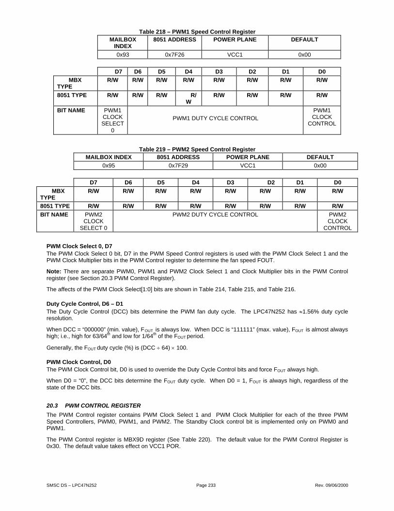
SMSC DS – LPC47N252 Page 233 Rev. 09/06/2000
Table 218 – PWM1 Speed Control RegisterMAILBOX
INDEX8051 ADDRESS POWER PLANE DEFAULT
0x93 0x7F26 VCC1 0x00
D7 D6 D5 D4 D3 D2 D1 D0
MBXTYPE
R/W R/W R/W R/W R/W R/W R/W R/W
8051 TYPE R/W R/W R/W R/W
R/W R/W R/W R/W
BIT NAME PWM1CLOCKSELECT
0
PWM1 DUTY CYCLE CONTROLPWM1CLOCK
CONTROL
Table 219 – PWM2 Speed Control RegisterMAILBOX INDEX 8051 ADDRESS POWER PLANE DEFAULT
0x95 0x7F29 VCC1 0x00
D7 D6 D5 D4 D3 D2 D1 D0
MBXTYPE
R/W R/W R/W R/W R/W R/W R/W R/W
8051 TYPE R/W R/W R/W R/W R/W R/W R/W R/W
BIT NAME PWM2CLOCK
SELECT 0
PWM2 DUTY CYCLE CONTROL PWM2CLOCK
CONTROL
PWM Clock Select 0, D7The PWM Clock Select 0 bit, D7 in the PWM Speed Control registers is used with the PWM Clock Select 1 and thePWM Clock Multiplier bits in the PWM Control register to determine the fan speed FOUT.
Note: There are separate PWM0, PWM1 and PWM2 Clock Select 1 and Clock Multiplier bits in the PWM Controlregister (see Section 20.3 PWM Control Register).
The affects of the PWM Clock Select[1:0] bits are shown in Table 214, Table 215, and Table 216.
Duty Cycle Control, D6 – D1The Duty Cycle Control (DCC) bits determine the PWM fan duty cycle. The LPC47N252 has ≈1.56% duty cycleresolution.
When DCC = “000000” (min. value), FOUT is always low. When DCC is “111111” (max. value), FOUT is almost alwayshigh; i.e., high for 63/64th and low for 1/64th of the FOUT period.
Generally, the FOUT duty cycle (%) is (DCC ÷ 64) × 100.
PWM Clock Control, D0The PWM Clock Control bit, D0 is used to override the Duty Cycle Control bits and force FOUT always high.
When D0 = “0”, the DCC bits determine the FOUT duty cycle. When D0 = 1, FOUT is always high, regardless of thestate of the DCC bits.
20.3 PWM CONTROL REGISTER
The PWM Control register contains PWM Clock Select 1 and PWM Clock Multiplier for each of the three PWMSpeed Controllers, PWM0, PWM1, and PWM2. The Standby Clock control bit is implemented only on PWM0 andPWM1.
The PWM Control register is MBX9D register (See Table 220). The default value for the PWM Control Register is0x30. The default value takes effect on VCC1 POR.

SMSC DS – LPC47N252 Page 234 Rev. 09/06/2000
Table 220 – PWM Control Register
MAILBOX INDEX 8051 ADDRESS POWER PLANE DEFAULT
0x9D 0x7F28 VCC1 0x30
D7 D6 D5 D4 D3 D2 D1 D0
MBXTYPE
R/W R/W R/W R/W R/W R/W R/W R/W
8051 TYPE R/W R/W R/W R/W R/W R/W R/W R/W
BIT NAME PWM2CLOCKMULTI-PLIER
PWM2CLOCK
SELECT 1
PWM1
STDBYCLOCK1
PWM0STDBYCLOCK1
PWM1CLOCKMULTI-PLIER
PWM0CLOCKMULTI-PLIER
PWM1CLOCK
SELECT 1
PWM0CLOCK
SELECT 1
PROGRAMMER’S NOTE1: The PWMx STDBY CLOCK bits, D4 and D5, should not be switched when PWRGD isinactive; i.e., when VCC2 = 0V.
PWM2 Clock Multiplier, D7The PWM2 Clock Multiplier bit, D7 is used with the PWM2 Clock Select 1 bit, D6 and the PWM2 Clock Select 0 bit,MBX95.7 to determine the PWM2 FOUT .
When the PWM2 Clock Multiplier bit = “0”, no clock multiplier is used. When the PWM2 Clock Multiplier bit = “1”, theclock speed determined by the PWM2 Clock Select [1:0] bits is doubled (Table 216 - PWM2 Speed ControlSummary.)
PWM2 Clock Select 1, D6The PWM2 Clock Select 1 bit, D6 is used with the PWM2 Clock Multiplier bit, D7 and the PWM2 Clock Select 0 bit,MBX95.7 to determine the PWM2 FOUT .
The affects of the Fan Clock Select [1:0] bits are shown in Table 216 - PWM2 Speed Control Summary.
PWM1 Stdby Clock, D5The PWM1 STDBY CLOCK bit D5 is used to determine the PWM1 controller clock source.
When the PWM1 STDBY CLOCK bit = “1”, the PWM1 controller clock source is the 32.768kHz RTC clock(VCC1/VCC2). The available PWM1 FOUT frequencies when D5 = “1” are shown in Table 214 – PWM0 and PWM1Speed Control Summary (STDBY Clock Bit = “0”).
When the PWM1 STDBY CLOCK bit = “0”, the PWM1 controller clock source is the system clock (VCC2). Theavailable PWM1 FOUT frequencies when D5 = “0” are shown in Table 214 – PWM0 and PWM1 Speed ControlSummary (STDBY Clock Bit = “0”).
The PWM1 STDBY CLOCK bit default = “1”.
PWM0 Stdby Clock, D4The PWM0 STDBY CLOCK bit, D4 is used to determine the PWM0 controller clock source.
When the PWM0 STDBY CLOCK bit = “1”, the PWM0 controller clock source is the 32.768kHz RTC clock(VCC1/VCC2). The available PWM0 FOUT frequencies when D4 = “1” are shown in Table 214 – PWM0 and PWM1Speed Control Summary (STDBY Clock Bit = “0”).
When the PWM0 STDBY CLOCK bit = “0”, the PWM0 controller clock source is the system clock (VCC2). Theavailable PWM0 FOUT frequencies when D4 = “0” are shown in Table 214 – PWM0 and PWM1 Speed ControlSummary (STDBY Clock Bit = “0”).
The PWM0 STDBY CLOCK bit default = “1”.
PWM1 Clock Multiplier, D3The PWM1 Clock Multiplier bit, D3 is used with the PWM1 Clock Select 1 bit, D1 and the PWM1 Clock Select 0 bit,MBX93.7 to determine the PWM1 FOUT when the PWM1 STDBY CLOCK select bit is “0”.
When the PWM1 Clock Multiplier bit = “0”, no clock multiplier is used. When the PWM1 Clock Multiplier bit = “1”, theclock speed determined by the PWM1 Clock Select [1:0] bits is doubled (Table 214 – PWM0 and PWM1 SpeedControl Summary (STDBY Clock Bit = “0”)).
The PWM1 Clock Multiplier bit does not affect the PWM1 FOUT when the PWM1 STDBY CLOCK select bit is “1”.
SMSC DS – LPC47N252 Page 235 Rev. 09/06/2000
PWM0 Clock Multiplier, D2The PWM0 Clock Multiplier bit, D2 is used with the PWM0 Clock Select 1 bit, D0 and the PWM0 Clock Select 0 bit,MBX92.7 to determine the PWM0 FOUT when the PWM0 STDBY CLOCK select bit is “0”.
When the PWM0 Clock Multiplier bit = “0”, no clock multiplier is used. When the PWM0 Clock Multiplier bit = “1”, theclock speed determined by the PWM0 Clock Select [1:0] bits is doubled (Table 214 – PWM0 and PWM1 SpeedControl Summary (STDBY Clock Bit = “0”)).
The PWM0 Clock Multiplier bit does not affect the PWM0 FOUT when the PWM0 STDBY CLOCK select bit is “1”.
PWM1 Clock Select 1, D1The PWM1 Clock Select 1 bit, D1 is used with the PWM1 Clock Multiplier bit, D3 and the PWM1 Clock Select 0 bit,MBX93.7 to determine the PWM1 FOUT .
The affects of the PWM1 Clock Select [1:0] bits are shown in Table 214 and Table 215.
PWM0 Clock Select 1, D0The PWM0 Clock Select 1 bit, D0 is used with the PWM0 Clock Multiplier bit, D2 and the PWM0 Clock Select 0 bit,MBX92.7 to determine the PWM0 FOUT .
The affects of the PWM1 Clock Select [1:0] bits are shown in Table 214 and Table 215.

SMSC DS – LPC47N252 Page 236 Rev. 09/06/2000
21 FAN TACHOMETER INTERFACE
21.1 FAN TACHOMETER OVERVIEW
The LPC47N252 implements a dual fan tachometer interface for systems with fans equipped with speed monitoringoutputs. The fan tachometer input pins are FAN_TACH1 and FAN_TACH2 (Table 2). These pins are alternatefunctions of the GPIO15 and GPIO16 pins, respectively (See Table 4 and MICS[11 bit in section 25.4.) The timebasefor the fan tachometer interface is the 32.768kHz RTC oscillator (FIGURE 57). A fan tachometer input gates the32.768 kHz RTC oscillator for one period of the input signal into an 8-bit counter. As shown in FIGURE 57, one fanrevolution, TR, consists of two fan tachometer pulses, TP. The fan tachometer interface can generate an 8051interrupt and wake event when the fan speed (RPM) drops below a predetermined value. The fan tachometerinterface is available when VCC2 is active and on the suspend supply, VCC1.
FIGURE 57 - FAN TACHOMETER INPUT & TIME-BASE
21.2 THEORY OF OPERATION
Each fan tachometer in the dual fan tachometer interface contains a Timebase Prescaler, a Fan Pulse Counter, aFan Pulse Counter Preload, a Fan Pulse Counter Read Latch, and a Fan Pulse Counter Threshold Detector(FIGURE 58). Detailed descriptions of these components follow in the subsections, below.
21.2.1 TIMEBASE PRESCALER
The timebase prescaler divides the fan tachometer timebase. The timebase prescaler can be used to account forseveral fan types (i.e., fans where the RPM values do not depend on two fan tachometer pulses per revolution) and awide range of fan speeds. The prescaler for each fan tachometer is programmable via the FAN TachometerTimebase Prescaler Register (see section 21.8 FAN Tachometer Timebase Prescaler Register, below). The choicesfor the timebase prescaler are 1, 2, 4 and 8; the default is 2.
21.2.2 FAN PULSE COUNTER AND READ LATCH
The fan pulse counter measures the fan pulse time, Tp, shown in FIGURE 57. The fan pulse counter is reset by therising edge of each fan tachometer input pulse and by writing the counter preload register. The fan pulse counterdoes not wrap. For example, when the counter reaches 0xFF, it remains at 0xFF until the counter is reset by the nextinput pulse or by writing the Preload register. The host can read the last maximum fan pulse counter value using the
TR
TP
F = 32kHz Prescaler
FanTachometerInput
Time-base
TR = Revolution Time = 60/RPM (sec)TP = Pulse Time = TR/2 (Two Pulses Per Revolution)

SMSC DS – LPC47N252 Page 237 Rev. 09/06/2000
FAN1 and FAN2 Read Latch registers (see sections 21.3 and 21.4, below). The fan pulse counter equation is shownin Table 218. The factor of _ in first term of the equation accounts for the fan Revolution Time TR (i.e., two pulses perrevolution as shown in FIGURE 57). The numerator of the second term is derived by multiplying the 32.768kHztimebase by 60sec/min. The denominator of the second term is the product of the fan RPM and the timebaseprescaler.
21.2.3 FAN PULSE COUNTER THRESHOLD DETECTOR
The fan pulse counter threshold detector consists of the two ‘AND’ed MSB outputs of the fan pulse counter. Thiscorresponds to an upper limit for the fan pulse counter of 192. The outputs of the fan pulse counter thresholddetectors are always asserted when the fan pulse count equals or exceeds 192. The outputs of the fan pulse counterthreshold detectors are always deasserted when the fan pulse count is less than 192. If enabled, the 8051 receivesan interrupt when the outputs of the fan pulse counter threshold detectors are asserted. For a description of the FANTACH1 and FAN TACH2 8051 interrupt registers see section 21.9 8051 FAN Tachometer Interrupt Registers, below.
Table 221 – Fan Pulse Counter Equation
1 1.966 x 10⁶FAN PULSE COUNT =2
×RPM x PRESCALER
21.2.4 FAN PULSE COUNTER PRELOAD
The fan pulse counter preload is the initial value for the fan pulse counter which is used to scale the count so that thevalue of 192 corresponds to the “lower limit” of the threshold RPM. The fan pulse counter is initialized with thepreload on the rising edge of the fan tachometer input pulse. Typically, the fan pulse counter preload value will be192 minus the fan pulse count of the desired RPM trigger threshold. The counter preload value is programmable foreach fan tachometer via the FAN1 and FAN2 Preload Registers (see sections 21.5 and 21.7, below). By setting thefan pulse counter preload value and the timebase prescaler appropriately, the 8051 can be interrupted when the fanspeed reaches the desired percentage of the nominal RPM to indicate fan failures for a wide range of fan types andspeeds (see section 21.3 Example, below).
FIGURE 58 - FAN TACHOMETER BLOCK DIAGRAM
PRESCALERFAN PULSECOUNTER
PRELOAD
READ LATCH
SYNC 8051
32 kHz
MSB
FAN_TACHn − LOAD

SMSC DS – LPC47N252 Page 238 Rev. 09/06/2000
21.3 EXAMPLE
Table 222 illustrates a fan tachometer interface programming example for a 4400 RPM nominal fan. In this example,the system designer has specified a fan counter preload value of 33 so that the 8051 will be alerted when the fanspeed drops below 70% nominal RPM. Note: the values in Table 222 are based on a 2 pulse/revolution fantachometer output with the default timebase prescaler of 2.
Table 222 – 4400 RPM Fan Tachometer Example
RPM
(TR)
PULSETIME1
(TP)
FANPULSE
COUNT2PRELOAD FAN PULSE COUNT +
PRELOADDESCRIPTION 8051
INTERRUPT
4400 6.8 ms 111 144 Nominal RPM
3960 7.6 ms 124 157 90% NominalRPM
3520 8.5 ms 139 172 80% NominalRPM
NO
3080 9.7 ms 159 192 70% NominalRPM
2640 11.4 ms 186 219 60% NominalRPM
2200 13.6 ms 223
33
>255 (maximum count) 50% NominalRPM
YES
Note1 There are 2 fan tachometer pulses per fan revolution: TP = 60 ÷ (2 × RPM).
Note2 The timebase prescaler = 2.
21.4 FAN1 READ LATCH REGISTER
The FAN1 read latch register (Table 223) stores the maximum last fan pulse counter value before the rising edge ofthe next FAN1 tachometer input pulse. The fan pulse count is computed from the equation in Table 218. The FAN1read latch register value may not be valid for up to 2 fan tachometer input pulses following a write to the preloadregister.
Table 223 - FAN1 Read Latch RegisterHOST ADDRESS N/A
8051 ADDRESS 0x7F9B
POWER VCC1
DEFAULT 0x00
D7 D6 D5 D4 D3 D2 D1 D0
HOST TYPE - - - - - - - -
8051 TYPE R R R R R R R R
BIT NAME D7 D6 D5 D4 D3 D2 D1 D0

SMSC DS – LPC47N252 Page 239 Rev. 09/06/2000
21.5 FAN2 READ LATCH REGISTER
The FAN2 read latch register (Table 224) stores the last (maximum) fan pulse counter value before the rising edge ofthe FAN2 tachometer input pulse. The fan pulse count is computed from the equation in Table 221. The FAN2 readlatch register value may not be valid for up to 2 fan tachometer input pulses following a write to the preload register.
Table 224 – FAN2 Read Latch RegisterHOST ADDRESS N/A
8051 ADDRESS 0x7F9C
POWER VCC1
DEFAULT 0x00
D7 D6 D5 D4 D3 D2 D1 D0
HOST TYPE - - - - - - - -
8051 TYPE R R R R R R R R
BIT NAME D7 D6 D5 D4 D3 D2 D1 D0
21.6 FAN1 PULSE COUNTER PRELOAD REGISTER
The FAN1 pulse counter preload register (Table 225) stores the preload value used in the computation of the FAN1pulse count (see section 21.2.4 Fan Pulse Counter Preload, above). The fan pulse count is computed from theequation in Table 221. Writing to the FAN1 pulse counter preload register resets the FAN1 pulse counter. The FAN1read latch register value may not be valid for up to 2 fan tachometer input pulses following a write to the FAN1 pulsecounter preload register.
Table 225 – FAN1 Pulse Counter Preload RegisterHOST ADDRESS N/A
8051 ADDRESS 0x7F9D
POWER VCC1
DEFAULT 0x00
D7 D6 D5 D4 D3 D2 D1 D0
HOST TYPE - - - - - - - -
8051 TYPE R/W R/W R/W R/W R/W R/W R/W R/W
BIT NAME D7 D6 D5 D4 D3 D2 D1 D0
21.7 FAN2 PRELOAD REGISTER
The FAN2 pulse counter preload register (Table 226) stores the preload value used in the computation of the FAN2pulse count (see section 21.2.4 Fan Pulse Counter Preload, above). The fan pulse count is computed from theequation in Table 221. Writing to the FAN2 pulse counter preload register resets the FAN2 pulse counter. The FAN2read latch register value may not be valid for up to 2 fan tachometer input pulses following a write to the FAN2 pulsecounter preload register.

SMSC DS – LPC47N252 Page 240 Rev. 09/06/2000
Table 226 – FAN2 Pulse Counter Preload RegisterHOST ADDRESS N/A
8051 ADDRESS 0x7F9E
POWER VCC1
DEFAULT 0x00
D7 D6 D5 D4 D3 D2 D1 D0
HOST TYPE - - - - - - - -
8051 TYPE R/W R/W R/W R/W R/W R/W R/W R/W
BIT NAME D7 D6 D5 D4 D3 D2 D1 D0
21.8 FAN TACHOMETER TIMEBASE PRESCALER REGISTER
The fan tachometer timebase prescaler register is shown below in Table 227. The timebase prescaler is described insection 21.2.1 Timebase Prescaler, above.
Table 227 – FAN Tachometer Timebase Prescaler RegisterHOST ADDRESS N/A
8051 ADDRESS 0x7F9F
POWER VCC1
DEFAULT 0x05
D7 D6 D5 D4 D3 D2 D1 D0
HOST TYPE - - - - - - - -
8051 TYPE R R R R R/W R/W R/W R/W
BIT NAME RESERVED FAN2 PRESCALER
00: Prescaler = 101: Prescaler = 2 (DEFAULT)10: Prescaler = 4
11: Prescaler = 8
FAN1 PRESCALER
00: Prescaler = 101: Prescaler = 2 (DEFAULT)10: Prescaler = 4
11: Prescaler = 8
21.9 8051 FAN TACHOMETER INTERRUPT REGISTERS
The FAN TACH1 and FAN TACH 2 interrupts appear in the 8051 Wake Up SRC 7 and Wake Up MSK 7 registersSee FIGURE 14, FIGURE 15, Table 118, and Table 125 in section 11.9, 8051 Interrupts, which starts on page 136.
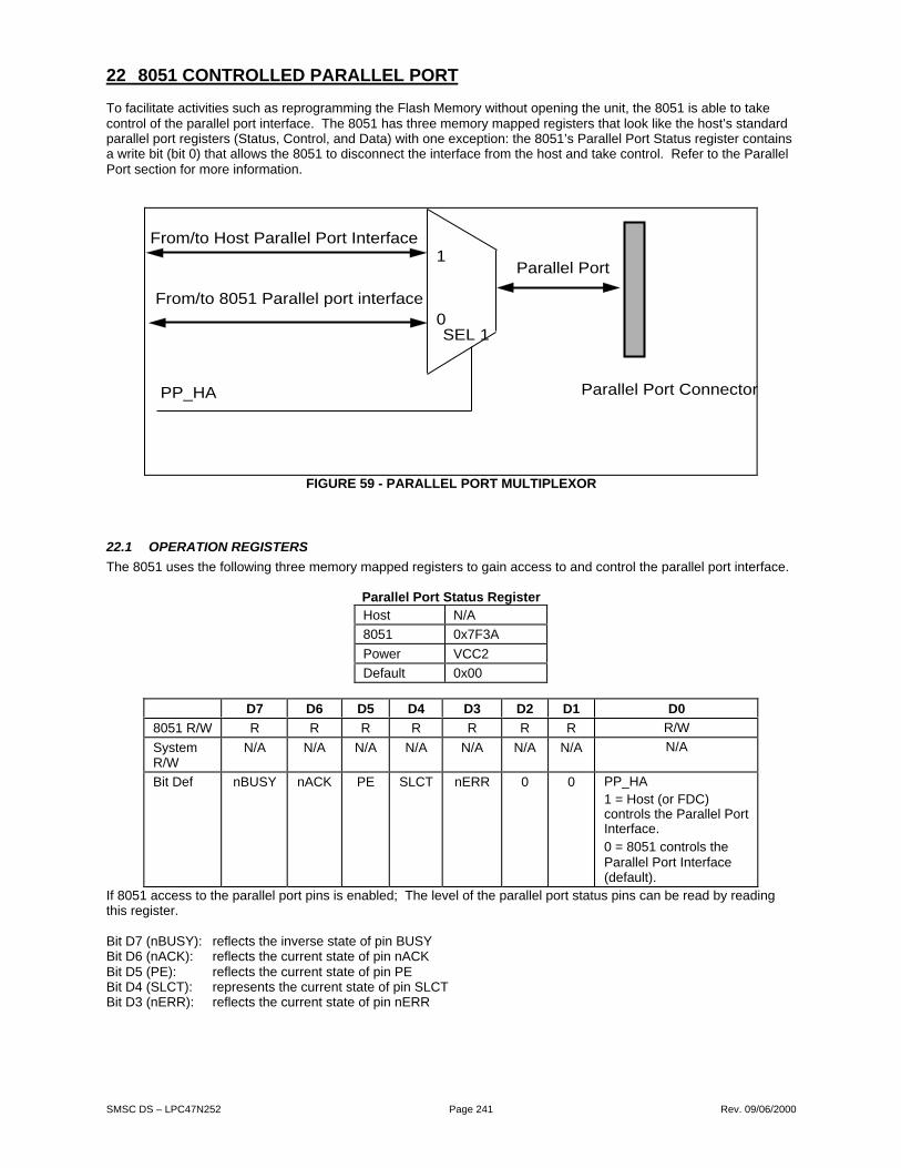
SMSC DS – LPC47N252 Page 241 Rev. 09/06/2000
22 8051 CONTROLLED PARALLEL PORT
To facilitate activities such as reprogramming the Flash Memory without opening the unit, the 8051 is able to takecontrol of the parallel port interface. The 8051 has three memory mapped registers that look like the host’s standardparallel port registers (Status, Control, and Data) with one exception: the 8051’s Parallel Port Status register containsa write bit (bit 0) that allows the 8051 to disconnect the interface from the host and take control. Refer to the ParallelPort section for more information.
SEL 1
From/to Host Parallel Port Interface
Parallel Port
Parallel Port Connector
From/to 8051 Parallel port interface
PP_HA
1
0
FIGURE 59 - PARALLEL PORT MULTIPLEXOR
22.1 OPERATION REGISTERS
The 8051 uses the following three memory mapped registers to gain access to and control the parallel port interface.
Parallel Port Status RegisterHost N/A
8051 0x7F3A
Power VCC2
Default 0x00
D7 D6 D5 D4 D3 D2 D1 D0
8051 R/W R R R R R R R R/W
SystemR/W
N/A N/A N/A N/A N/A N/A N/A N/A
Bit Def nBUSY nACK PE SLCT nERR 0 0 PP_HA1 = Host (or FDC)controls the Parallel PortInterface.0 = 8051 controls theParallel Port Interface(default).
If 8051 access to the parallel port pins is enabled; The level of the parallel port status pins can be read by readingthis register.
Bit D7 (nBUSY): reflects the inverse state of pin BUSYBit D6 (nACK): reflects the current state of pin nACKBit D5 (PE): reflects the current state of pin PEBit D4 (SLCT): represents the current state of pin SLCTBit D3 (nERR): reflects the current state of pin nERR

SMSC DS – LPC47N252 Page 242 Rev. 09/06/2000
Parallel Port Control RegisterHost N/A
8051 0x7F3B
Power VCC2
Default 0x00
D7 D6 D5 D4 D3 D2 D1 D0
8051 R/W R/W R/W R/W R/W R/W R/W R/W R/W
SystemR/W
N/A N/A N/A N/A N/A N/A N/A N/A
Bit Def 0 0 PCD 0 SLCTIN nINIT ALF STROBE
If 8051 access to the parallel port pins is enabled, the value of STROBE, ALF and SLCTIN are inverted and outputonto the parallel port control pins. The value of nINIT is output onto the parallel port control pins. If PCD (ParallelControl Direction) = 0, the data bus is output. If PCD = 1 the parallel port data bus is floating to allow read data in.
Parallel Port Data RegisterHost N/A
8051 0x7F3C
Power VCC2
Default 0x00
D7 D6 D5 D4 D3 D2 D1 D0
8051 R/W R/W R/W R/W R/W R/W R/W R/W R/W
System R/W N/A N/A N/A N/A N/A N/A N/A N/A
Bit Def PD7 PD6 PD5 PD4 PD3 PD2 PD1 PD0
If 8051 access to the parallel port pins is enabled; When read, this register reads the logic levels on the parallel portpins.

SMSC DS – LPC47N252 Page 243 Rev. 09/06/2000
23 HOST CONTROLLED IR PORT
It is possible to give direct control of the IRRX and IRTX pins to the Host CPU by setting bit 2 of the Multiplexing_1Register. The Host communicates to the pins through its memory mapped IR Data Register shown here.
IR Data RegisterHost MBX 0x98
8051 N/A
Power VCC2
Default 0x00
D7-D2 D1 D0
8051 R/W N/A N/A N/A
System R/W R/W R R/W
Bit Def Reserved IR_REC IR_TX
Bit 1 and bit 0 are don’t care if MISC2 is reset. (These bits are multiplexed onto the IRTX and IRRX pins whenMISC2 is set). See section 25.3, Multiplexing_1 Register – MISC[7:0].Note that MISC7 allows the control of the IRRX2/GPIO8 and IRTX2/GPIO9 pins. If the IRRX2 and IRTX2 pins areused for IR, then this allows the IR interface access to be switched between the IRCC 2.0 block and the 8051.

SMSC DS – LPC47N252 Page 244 Rev. 09/06/2000
24 GPIO INTERFACE
24.1 OVERVIEW
The LPC47N252 includes three general purpose I/O pin types: Forty-two 8051 non-SFR GPIOs, Sixteen 8051 SFR-addressable GPIOs, and Twenty-four LPC/8051-addressable GPIOs (Table 228).
The 8051 non-SFR GPIOs are described below in section 24.2, 8051 Non-SFR GPIOs. The LPC/8051-addressableGPIOs are described below in section 24.4, LPC/8051-Addressable GPIOs. The SFR-addressable GPIOs aredescribed in section 24.5, Bit-wise Addressable 8051 SFR GPIOs.
Sixteen of the Twenty-four LPC/8051-addressable GPIOs can also be configured as GPIO Pass-Through Ports (seesection 24.6, GPIO PASS-THROUGH PORTS). Eight of the Twenty-four LPC/8051-addressable GPIOs cangenerate 8051 interrupts and wake events. See FIGURE 14, FIGURE 15, Table 118, and Table 125 in section 11.9,8051 Interrupts, which starts on page 136.
Table 228 – LPC47N252 GPIO Types
ITEM TYPE PIN NAMESWAKE
CAPABLEBUFFERMODES2
1. SGPIO30 N PP
2. SGPIO31 N PP
3. SGPIO32 N PP
4. SGPIO33 N PP
5. SGPIO34 N PP
6. SGPIO35 N PP
7. SGPIO36 N PP
8. SGPIO37 N PP
9. SGPIO40 N PP
10. SGPIO41 N PP
11. SGPIO42 N PP
12. SGPIO43 N PP
13. SGPIO44 N PP
14. SGPIO45 N PP
15. SGPIO46 N PP
16.
8051 SFR
SGPIO47 N PP
17. KSO12/OUT8/KBRST N PP
18. KSO13/GPIO18 N PP
19. OUT0 N PP/OD
20. OUT1/nIRQ8 N PP
21. OUT2 N PP
22. OUT3 N PP
23. OUT4 N PP
24. OUT5/nDS1/KBRST N PP
25. OUT6/nMTR1 N PP
26. OUT7/nSMI N PP
27. OUT8/KBRST N PP
28. OUT9 N PP
29. OUT10/PWM0 N PP
30. OUT11/PWM1 N PP
31. IN0 (WK_EE4) Y PP
32. IN1 (WK_EE2) Y PP
33. IN2 (WK_EE3) Y PP
34. IN3 (nGPWKUP) Y PP
35.
8051 (non-SFR)
IN4 (WK_SE00) Y PP
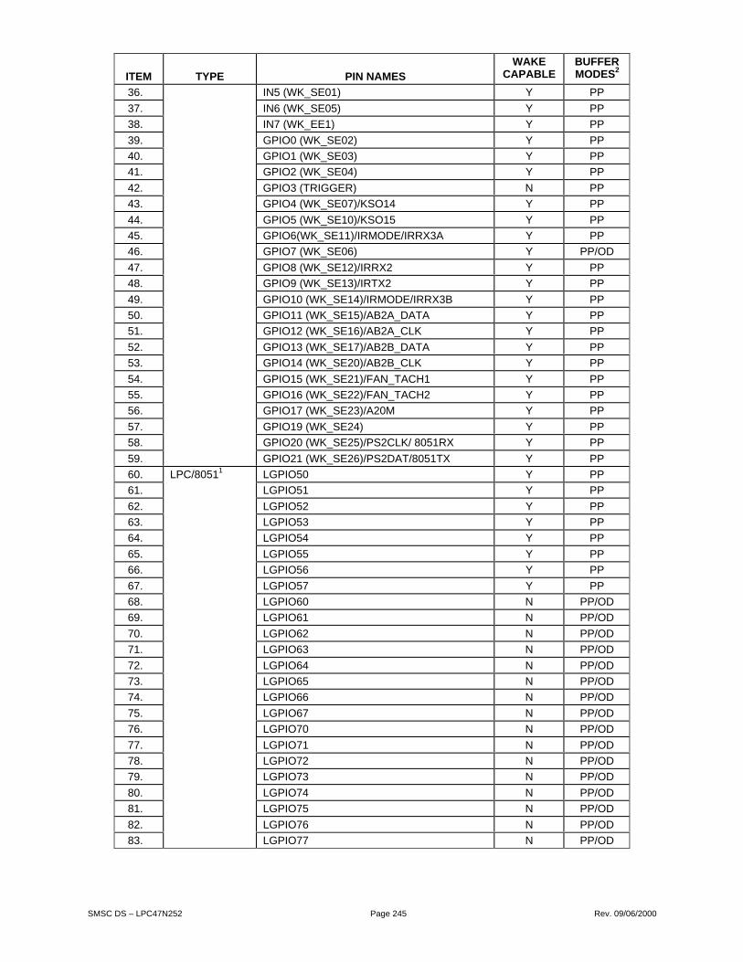
SMSC DS – LPC47N252 Page 245 Rev. 09/06/2000
ITEM TYPE PIN NAMESWAKE
CAPABLEBUFFERMODES2
36. IN5 (WK_SE01) Y PP
37. IN6 (WK_SE05) Y PP
38. IN7 (WK_EE1) Y PP
39. GPIO0 (WK_SE02) Y PP
40. GPIO1 (WK_SE03) Y PP
41. GPIO2 (WK_SE04) Y PP
42. GPIO3 (TRIGGER) N PP
43. GPIO4 (WK_SE07)/KSO14 Y PP
44. GPIO5 (WK_SE10)/KSO15 Y PP
45. GPIO6(WK_SE11)/IRMODE/IRRX3A Y PP
46. GPIO7 (WK_SE06) Y PP/OD
47. GPIO8 (WK_SE12)/IRRX2 Y PP
48. GPIO9 (WK_SE13)/IRTX2 Y PP
49. GPIO10 (WK_SE14)/IRMODE/IRRX3B Y PP
50. GPIO11 (WK_SE15)/AB2A_DATA Y PP
51. GPIO12 (WK_SE16)/AB2A_CLK Y PP
52. GPIO13 (WK_SE17)/AB2B_DATA Y PP
53. GPIO14 (WK_SE20)/AB2B_CLK Y PP
54. GPIO15 (WK_SE21)/FAN_TACH1 Y PP
55. GPIO16 (WK_SE22)/FAN_TACH2 Y PP
56. GPIO17 (WK_SE23)/A20M Y PP
57. GPIO19 (WK_SE24) Y PP
58. GPIO20 (WK_SE25)/PS2CLK/ 8051RX Y PP
59. GPIO21 (WK_SE26)/PS2DAT/8051TX Y PP
60. LGPIO50 Y PP
61. LGPIO51 Y PP
62. LGPIO52 Y PP
63. LGPIO53 Y PP
64. LGPIO54 Y PP
65. LGPIO55 Y PP
66. LGPIO56 Y PP
67. LGPIO57 Y PP
68. LGPIO60 N PP/OD
69. LGPIO61 N PP/OD
70. LGPIO62 N PP/OD
71. LGPIO63 N PP/OD
72. LGPIO64 N PP/OD
73. LGPIO65 N PP/OD
74. LGPIO66 N PP/OD
75. LGPIO67 N PP/OD
76. LGPIO70 N PP/OD
77. LGPIO71 N PP/OD
78. LGPIO72 N PP/OD
79. LGPIO73 N PP/OD
80. LGPIO74 N PP/OD
81. LGPIO75 N PP/OD
82. LGPIO76 N PP/OD
83.
LPC/80511
LGPIO77 N PP/OD

SMSC DS – LPC47N252 Page 246 Rev. 09/06/2000
Note1: These pins can be controlled by the LPC Host or the 8051 (see section 24.4 LPC/8051-Addressable GPIOs,below).
Note2: PP = Push-Pull (Totem Pole) Outputs; PP/OD = Selectable Push-Pull or Open-Drain Outputs (see section24.4.3.5 Programmable Buffer Type Registers, below).
24.2 8051 NON-SFR GPIOS
The 8051 non-SFR GPIO pins are GPIO 0 – 21, IN 0 – 7 and OUT 0 – 11. Some 8051 non-SFR GPIOs aremultiplexed with alternate functions (see Table 228 – LPC47N252 GPIO Types on page 244 and Table 4 - AlternateFunction Pins on page 15.)
All 8051 non-SFR registers are powered by VCC1. The following pins will tri-state to prevent back-biasing of externalcircuitry when they are configured as alternate function outputs and PWRGD is inactive (i.e. VCC2 is 0v): GPIO6,GPIO10, OUT1, OUT5 - OUT9, GPIO17, GPIO20, GPIO21, and KSO12.
GPIO9 defaults to “output”, “low”, for both the default (GPIO) function and the alternate (IRTX) function, regardless ofthe state of PWRGD. This is done to prevent infrared transceiver damage.
PROGRAMMER’S NOTE: the direction of alternate function pins that are multiplexed with general purpose I/O pins(i.e., where the GPIO function is the default), is determined by the GPIO direction bit. For example if the KS014function of GPIO4 is selected, bit 4 in GPIO Direction Register A must be set to “1”. This rule does not apply todefault non-GPIO pin functions that may have a GPIO as an alternate function.
GPIO OUT REG BIT
GPIO IN REG BIT
GPIO DIR BIT
ALT FUNCControl bit
ALT FUNC OUTPUT
GPIO PIN
1
0
ALT FUNC INPUT
nRDnWR
FIGURE 60 – 8051 NON-SFR GPIO BLOCK DIAGRAM
24.3 8051 NON-SFR REGISTERS
Table 229 - GPIO Direction Register AHOST ADDRESS N/A
8051 ADDRESS 0x7F18
POWER VCC1
DEFAULT 0x00
D7 D6 D5 D4 D3 D2 D1 D0
HOST TYPE - - - - - - - -
8051 TYPE R/W R/W R/W R/W R/W R/W R/W R/W
BIT NAME GPIO71=output0=input
GPIO61=output0=input
GPIO51=output0=input
GPIO41=output0=input
GPIO31=output0=input
GPIO21=output0=input
GPIO11=output0=input
GPIO01=output0=input

SMSC DS – LPC47N252 Page 247 Rev. 09/06/2000
Table 230 - GPIO Input Register AHOST ADDRESS N/A
8051 ADDRESS 0x7F1A
POWER VCC1
DEFAULT N/A
D7 D6 D5 D4 D3 D2 D1 D0
HOST TYPE - - - - - - - -
8051 TYPE R R R R R R R R
BIT NAME status ofpin
GPIO7
status ofpin
GPIO6
status ofpin
GPIO5
status ofpin
GPIO4
status ofpin
GPIO3
status ofpin
GPIO2
status ofpin
GPIO1
status ofpin
GPIO0
Table 231 - GPIO Output Register AHOST ADDRESS N/A
8051 ADDRESS 0x7F19
POWER VCC1
DEFAULT 0x00
D7 D6 D5 D4 D3 D2 D1 D0
HOST TYPE - - - - - - - -
8051 TYPE R/W R/W R/W R/W R/W R/W R/W R/W
BIT NAME GPIO7 GPIO6 GPIO5 GPIO4 GPIO3 GPIO2 GPIO1 GPIO0
Table 232 - GPIO Direction Register BHOST ADDRESS N/A
8051 ADDRESS 0x7F1B
POWER VCC1
DEFAULT 0x00
D7 D6 D5 D4 D3 D2 D1 D0
HOST TYPE - - - - - - - -
8051 TYPE R/W R/W R/W R/W R/W R/W R/W R/W
BIT NAME GPIO151=output0=input
GPIO14
1=output0=input
GPIO13
1=output0=input
GPIO12
1=output0=input
GPIO11
1=output0=input
GPIO10
1=output0=input
GPIO9
1=output0=input
GPIO8
1=output0=input
Table 233 - GPIO Output Register BHOST ADDRESS N/A
8051 ADDRESS 0x7F1C
POWER VCC1
DEFAULT 0x00
D7 D6 D5 D4 D3 D2 D1 D0
HOST TYPE - - - - - - - -
8051 TYPE R/W R/W R/W R/W R/W R/W R/W R/W
BIT NAME GPIO 15 GPIO 14 GPIO 13 GPIO 12 GPIO 11 GPIO 10 GPIO 9 GPIO 8

SMSC DS – LPC47N252 Page 248 Rev. 09/06/2000
Table 234 - GPIO Input Register BHOST ADDRESS N/A
8051 ADDRESS 0x7F1D
POWER VCC1
DEFAULT N/A
D7 D6 D5 D4 D3 D2 D1 D0
HOST TYPE - - - - - - - -
8051 TYPE R R R R R R R R
BIT NAME status ofpin
GPIO15
status ofpin
GPIO14
status ofpin
GPIO13
status ofpin
GPIO12
status ofpin
GPIO11
status ofpin
GPIO10
status ofpin
GPIO9
status ofpin
GPIO8
Table 235 - GPIO Direction Register CHOST ADDRESS N/A
8051 ADDRESS 0x7F1E
POWER VCC1
DEFAULT 0x00
D7 D6 D5 D4 D3 D2 D1 D0
HOST TYPE - - - - - - - -
8051 TYPE R/W R/W R/W R/W R/W R/W R/W R/W
BIT NAME0 0
GPIO211=output
0=input
GPIO201=output
0=input
GPIO191=output
0=input
GPIO181=output
0=input
GPIO171=output
0=input
GPIO161=output
0=input
Table 236 - GPIO Output Register CHOST ADDRESS N/A
8051 ADDRESS 0x7F1F
POWER VCC1
DEFAULT 0x00
D7 D6 D5 D4 D3 D2 D1 D0
HOST TYPE - - - - - - - -
8051 TYPE R/W R/W R/W R/W R/W R/W R/W R/W
BIT NAME 0 0 GPIO21 GPIO20 GPIO19 GPIO18 GPIO17 GPIO16
Table 237 - GPIO Input Register CHOST ADDRESS N/A
8051 ADDRESS 0x7F20
POWER VCC1
DEFAULT N/A
D7 D6 D5 D4 D3 D2 D1 D0
HOST TYPE - - - - - - - -
8051 TYPE R R R R R R R R
BIT NAME0 0
status ofpin
GPIO21
status ofpin
GPIO20
status ofpin
GPIO19
status ofpin
GPIO18
status ofpin
GPIO17
status ofpin
GPIO16
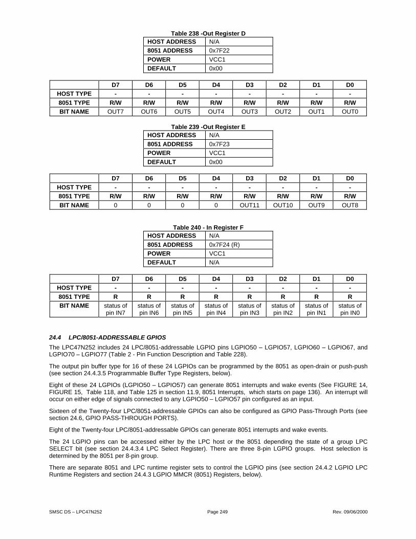
SMSC DS – LPC47N252 Page 249 Rev. 09/06/2000
Table 238 -Out Register DHOST ADDRESS N/A
8051 ADDRESS 0x7F22
POWER VCC1
DEFAULT 0x00
D7 D6 D5 D4 D3 D2 D1 D0
HOST TYPE - - - - - - - -
8051 TYPE R/W R/W R/W R/W R/W R/W R/W R/W
BIT NAME OUT7 OUT6 OUT5 OUT4 OUT3 OUT2 OUT1 OUT0
Table 239 -Out Register EHOST ADDRESS N/A
8051 ADDRESS 0x7F23
POWER VCC1
DEFAULT 0x00
D7 D6 D5 D4 D3 D2 D1 D0
HOST TYPE - - - - - - - -
8051 TYPE R/W R/W R/W R/W R/W R/W R/W R/W
BIT NAME 0 0 0 0 OUT11 OUT10 OUT9 OUT8
Table 240 - In Register FHOST ADDRESS N/A
8051 ADDRESS 0x7F24 (R)
POWER VCC1
DEFAULT N/A
D7 D6 D5 D4 D3 D2 D1 D0
HOST TYPE - - - - - - - -
8051 TYPE R R R R R R R R
BIT NAME status ofpin IN7
status ofpin IN6
status ofpin IN5
status ofpin IN4
status ofpin IN3
status ofpin IN2
status ofpin IN1
status ofpin IN0
24.4 LPC/8051-ADDRESSABLE GPIOS
The LPC47N252 includes 24 LPC/8051-addressable LGPIO pins LGPIO50 – LGPIO57, LGPIO60 – LGPIO67, andLGPIO70 – LGPIO77 (Table 2 - Pin Function Description and Table 228).
The output pin buffer type for 16 of these 24 LGPIOs can be programmed by the 8051 as open-drain or push-push(see section 24.4.3.5 Programmable Buffer Type Registers, below).
Eight of these 24 LGPIOs (LGPIO50 – LGPIO57) can generate 8051 interrupts and wake events (See FIGURE 14,FIGURE 15, Table 118, and Table 125 in section 11.9, 8051 Interrupts, which starts on page 136). An interrupt willoccur on either edge of signals connected to any LGPIO50 – LGPIO57 pin configured as an input.
Sixteen of the Twenty-four LPC/8051-addressable GPIOs can also be configured as GPIO Pass-Through Ports (seesection 24.6, GPIO PASS-THROUGH PORTS).
Eight of the Twenty-four LPC/8051-addressable GPIOs can generate 8051 interrupts and wake events.
The 24 LGPIO pins can be accessed either by the LPC host or the 8051 depending the state of a group LPCSELECT bit (see section 24.4.3.4 LPC Select Register). There are three 8-pin LGPIO groups. Host selection isdetermined by the 8051 per 8-pin group.
There are separate 8051 and LPC runtime register sets to control the LGPIO pins (see section 24.4.2 LGPIO LPCRuntime Registers and section 24.4.3 LGPIO MMCR (8051) Registers, below).

SMSC DS – LPC47N252 Page 250 Rev. 09/06/2000
The 8051 is responsible for configuring the LGPIO interface including the LPC SELECT bits and the output pin buffertype.
When the LPC host is selected to control an LGPIO pin and PWRGD is deasserted, the pin is tristated (input).Otherwise, the LGPIO channel direction and logic state is determined by the runtime registers of the selected host(see FIGURE 63 and Table 238).
Note 57: Regardless of the selected LGPIO pin host, the 8051 LGPIO input registers always reflect the state of theLPGIO pin (FIGURE 61). See Note 61 for the Pass Through Mode exception.
Table 241 - LPC Addressable GPIO Direction Control
8051DIR
LPCDIR
LPCSEL. PWRGD PIN DIR COMMENTS
1. X X 1 0 IN GPIO pin tristates (input) because GPIO isLPC type & VCC2 is invalid.
2. X 1 1 1 OUT
3. X 0 1 1 IN
GPIO pin is LPC type, follows LPC DIR bit,& VCC2 is valid.
4. 1 X 0 X OUT
5. 0 X 0 X IN
GPIO pin is 8051 type, follows 8051 DIR bit& VCC2 is not required.
FIGURE 61 - LPC ADDRESSABLE GPIO BLOCK DIAGRAM
Note: This figure is for illustration purposes only and is not intended to suggest specific implementationdetails.
1
08051 OUT
LPC OUT
LPC SELECT
LGPIOn
LPC DIR`
8051 DIR
PWRGD
LPC SELECT
8051 IN
LPC IN
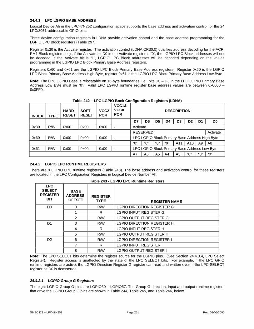
SMSC DS – LPC47N252 Page 251 Rev. 09/06/2000
24.4.1 LPC LGPIO BASE ADDRESS
Logical Device Ah in the LPC47N252 configuration space supports the base address and activation control for the 24LPC/8051-addressable GPIO pins
Three device configuration registers in LDNA provide activation control and the base address programming for theLGPIO LPC Block registers (Table 297).
Register 0x30 is the Activate register. The activation control (LDNA:CR30.0) qualifies address decoding for the ACPIPM1 Block registers; e.g., if the Activate bit D0 in the Activate register is “0”, the LGPIO LPC Block addresses will notbe decoded; if the Activate bit is “1”, LGPIO LPC Block addresses will be decoded depending on the valuesprogrammed in the LGPIO LPC Block Primary Base Address registers.
Registers 0x60 and 0x61 are the LGPIO LPC Block Primary Base Address registers. Register 0x60 is the LGPIOLPC Block Primary Base Address High Byte, register 0x61 is the LGPIO LPC Block Primary Base Address Low Byte.
Note: The LPC LGPIO Base is relocatable on 16-byte boundaries; i.e., bits D0 – D3 in the LPC LGPIO Primary BaseAddress Low Byte must be “0”. Valid LPC LGPIO runtime register base address values are between 0x0000 –0x0FF0.
Table 242 – LPC LGPIO Bock Configuration Registers (LDNA)
INDEX TYPE
HARDRESET
SOFTRESET
VCC2POR
VCC1&VCC0POR
DESCRIPTION
D7 D6 D5 D4 D3 D2 D1 D0
0x30 R/W 0x00 0x00 0x00 - Activate
RESERVED Activate
0x60 R/W 0x00 0x00 0x00 - LPC LGPIO Block Primary Base Address High Byte
“0” “0” “0” “0” A11 A10 A9 A8
0x61 R/W 0x00 0x00 0x00 - LPC LGPIO Block Primary Base Address Low Byte
A7 A6 A5 A4 A3 “0” “0” “0”
24.4.2 LGPIO LPC RUNTIME REGISTERS
There are 9 LGPIO LPC runtime registers (Table 243). The base address and activation control for these registersare located in the LPC Configuration Registers in Logical Device Number Ah.
Table 243 - LGPIO LPC Runtime RegistersLPC
SELECTREGISTER
BIT
BASEADDRESS
OFFSETREGISTER
TYPE REGISTER NAME
0 R/W LGPIO DIRECTION REGISTER G
1 R LGPIO INPUT REGISTER G
D0
2 R/W LGPIO OUTPUT REGISTER G
3 R/W LGPIO DIRECTION REGISTER H
4 R LGPIO INPUT REGISTER H
D1
5 R/W LGPIO OUTPUT REGISTER H
6 R/W LGPIO DIRECTION REGISTER I
7 R LGPIO INPUT REGISTER I
D2
8 R/W LGPIO OUTPUT REGISTER I
Note: The LPC SELECT bits determine the register source for the LGPIO pins. (See Section 24.4.3.4, LPC SelectRegister). Register access is unaffected by the state of the LPC SELECT bits. For example, if the LPC GPIOruntime registers are active, the LGPIO Direction Register G register can read and written even if the LPC SELECTregister bit D0 is deasserted.
24.4.2.1 LGPIO Group G Registers
The eight LGPIO Group G pins are LGPIO50 – LGPIO57. The Group G direction, input and output runtime registersthat drive the LGPIO Group G pins are shown in Table 244, Table 245, and Table 246, below.

SMSC DS – LPC47N252 Page 252 Rev. 09/06/2000
Table 244 – LPC LGPIO Direction Register GHOST ADDRESS BASE ADDR. + 0
8051 ADDRESS N/A
POWER VCC2
DEFAULT 0x00
D7 D6 D5 D4 D3 D2 D1 D0
HOST TYPE R/W R/W R/W R/W R/W R/W R/W R/W
8051 TYPE - - - - - - - -
BIT NAME LGPIO57
1=output0=input
LGPIO561=output0=input
LGPIO551=output0=input
LGPIO541=output0=input
LGPIO531=output0=input
LGPIO521=output0=input
LGPIO511=output0=input
LGPIO501=output0=input
Table 245 – LPC LGPIO Input Register GHOST ADDRESS BASE ADDR. + 1
8051 ADDRESS N/A
POWER VCC2
DEFAULT N/A
D7 D6 D5 D4 D3 D2 D1 D0
HOST TYPE R R R R R R R R
8051 TYPE - - - - - - - -
BIT NAME LGPIO57IN
LGPIO56IN
LGPIO55IN
LGPIO54IN
LGPIO53IN
LGPIO52IN
LGPIO51IN
LGPIO50IN
Table 246 – LPC LGPIO Output Register GHOST ADDRESS BASE ADDR. + 2
8051 ADDRESS N/A
POWER VCC2
DEFAULT 0x00
D7 D6 D5 D4 D3 D2 D1 D0
HOST TYPE R/W R/W R/W R/W R/W R/W R/W R/W
8051 TYPE - - - - - - - -
BIT NAME LGPIO57OUT
LGPIO56OUT
LGPIO55
OUT
LGPIO54
OUT
LGPIO53
OUT
LGPIO52
OUT
LGPIO51
OUT
LGPIO50
OUT
24.4.2.2 LGPIO Group H Registers
The eight LGPIO Group H pins are LGPIO60 – LGPIO67. The Group H direction, input and output runtime registersthat drive the LGPIO Group H pins are shown in Table 244, Table 245 and Table 246. Eight GPIO Pass-ThroughPorts can multiplex LGPIO Group G (see section 24.4.3.1) with LGPIO Group H. See Section 24.6 on page 261 fordescription of the GPIO PASS-THROUGH PORTS function.

SMSC DS – LPC47N252 Page 253 Rev. 09/06/2000
Table 247 – LPC LGPIO Direction Register HHOST ADDRESS BASE ADDR. + 3
8051 ADDRESS N/A
POWER VCC2
DEFAULT 0x00
D7 D6 D5 D4 D3 D2 D1 D0
HOST TYPE R/W R/W R/W R/W R/W R/W R/W R/W
8051 TYPE - - - - - - - -
BIT NAME LGPIO67
1=output0=input
LGPIO661=output0=input
LGPIO651=output0=input
LGPIO641=output0=input
LGPIO631=output0=input
LGPIO621=output0=input
LGPIO611=output0=input
LGPIO601=output0=input
Table 248 – LPC LGPIO Input Register HHOST ADDRESS BASE ADDR. + 4
8051 ADDRESS N/A
POWER VCC2
DEFAULT N/A
D7 D6 D5 D4 D3 D2 D1 D0
HOST TYPE R R R R R R R R
8051 TYPE - - - - - - - -
BIT NAME LGPIO67IN
LGPIO66IN
LGPIO65IN
LGPIO64IN
LGPIO63IN
LGPIO62IN
LGPIO61IN
LGPIO60IN
Table 249 – LPC LGPIO Output Register HHOST ADDRESS BASE ADDR. + 5
8051 ADDRESS N/A
POWER VCC2
DEFAULT 0x00
D7 D6 D5 D4 D3 D2 D1 D0
HOST TYPE R/W R/W R/W R/W R/W R/W R/W R/W
8051 TYPE - - - - - - - -
BIT NAME LGPIO67OUT
LGPIO66OUT
LGPIO65
OUT
LGPIO64
OUT
LGPIO63
OUT
LGPIO62
OUT
LGPIO61
OUT
LGPIO60
OUT
24.4.2.3 LGPIO Group I Registers
The eight LGPIO Group I pins are LGPIO70 – LGPIO77. The Group I direction, input and output runtime registersthat drive the LGPIO Group I pins are shown in Table 250, Table 251 and Table 252, below.

SMSC DS – LPC47N252 Page 254 Rev. 09/06/2000
Table 250 – LPC LGPIO Direction Register IHOST ADDRESS BASE ADDR. + 6
8051 ADDRESS N/A
POWER VCC2
DEFAULT 0x00
D7 D6 D5 D4 D3 D2 D1 D0
HOST TYPE R/W R/W R/W R/W R/W R/W R/W R/W
8051 TYPE - - - - - - - -
BIT NAME LGPIO77
1=output0=input
LGPIO761=output0=input
LGPIO751=output0=input
LGPIO741=output0=input
LGPIO731=output0=input
LGPIO721=output0=input
LGPIO711=output0=input
LGPIO701=output0=input
Table 251 - LPC LGPIO Input Register IHOST ADDRESS BASE ADDR. + 7
8051 ADDRESS N/A
POWER VCC2
DEFAULT N/A
D7 D6 D5 D4 D3 D2 D1 D0
HOST TYPE R R R R R R R R
8051 TYPE - - - - - - - -
BIT NAME LGPIO77IN
LGPIO76IN
LGPIO75IN
LGPIO74IN
LGPIO73IN
LGPIO72IN
LGPIO71IN
LGPIO70IN
Table 252 - LPC LGPIO Output Register IHOST ADDRESS BASE ADDR. + 8
8051 ADDRESS N/A
POWER VCC2
DEFAULT 0x00
D7 D6 D5 D4 D3 D2 D1 D0
HOST TYPE R/W R/W R/W R/W R/W R/W R/W R/W
8051 TYPE - - - - - - - -
BIT NAME LGPIO77OUT
LGPIO76OUT
LGPIO75
OUT
LGPIO74
OUT
LGPIO73
OUT
LGPIO72
OUT
LGPIO71
OUT
LGPIO70
OUT
24.4.3 LGPIO MMCR (8051) REGISTERS
There are 12 LGPIO MMCR (8051) registers (Table 253). There is also a register to control the buffer type for two ofthe standard 8051 GPIO pins. These registers provide 8051 runtime access, host configuration and buffer typecontrol for the LGPIO interface pins.
Table 253 - LGPIO MMCR (8051) Registers Summary8051
MMCRADDRESS
REGISTERTYPE 8051 MMCR REGISTER NAME
1. 0x7FA0 R/W LGPIO DIRECTION REGISTER G
2. 0x7FA1 R LGPIO INPUT REGISTER G
3. 0x7FA2 R/W LGPIO OUTPUT REGISTER G
4. 0x7FA3 R/W LGPIO DIRECTION REGISTER H
5. 0x7FA4 R LGPIO INPUT REGISTER H
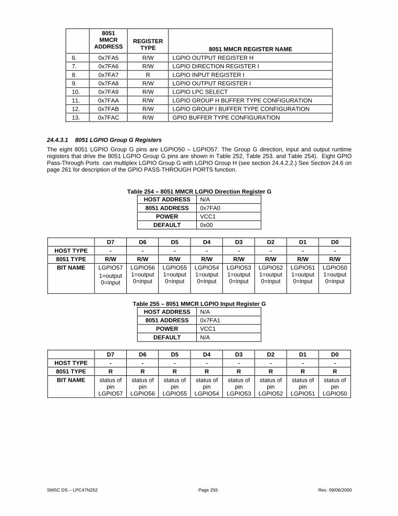
SMSC DS – LPC47N252 Page 255 Rev. 09/06/2000
8051MMCR
ADDRESSREGISTER
TYPE 8051 MMCR REGISTER NAME
6. 0x7FA5 R/W LGPIO OUTPUT REGISTER H
7. 0x7FA6 R/W LGPIO DIRECTION REGISTER I
8. 0x7FA7 R LGPIO INPUT REGISTER I
9. 0x7FA8 R/W LGPIO OUTPUT REGISTER I
10. 0x7FA9 R/W LGPIO LPC SELECT
11. 0x7FAA R/W LGPIO GROUP H BUFFER TYPE CONFIGURATION
12. 0x7FAB R/W LGPIO GROUP I BUFFER TYPE CONFIGURATION
13. 0x7FAC R/W GPIO BUFFER TYPE CONFIGURATION
24.4.3.1 8051 LGPIO Group G Registers
The eight 8051 LGPIO Group G pins are LGPIO50 – LGPIO57. The Group G direction, input and output runtimeregisters that drive the 8051 LGPIO Group G pins are shown in Table 252, Table 253, and Table 254). Eight GPIOPass-Through Ports can multiplex LGPIO Group G with LGPIO Group H (see section 24.4.2.2.) See Section 24.6 onpage 261 for description of the GPIO PASS-THROUGH PORTS function.
Table 254 – 8051 MMCR LGPIO Direction Register GHOST ADDRESS N/A
8051 ADDRESS 0x7FA0
POWER VCC1
DEFAULT 0x00
D7 D6 D5 D4 D3 D2 D1 D0
HOST TYPE - - - - - - - -
8051 TYPE R/W R/W R/W R/W R/W R/W R/W R/W
BIT NAME LGPIO57
1=output0=input
LGPIO561=output0=input
LGPIO551=output0=input
LGPIO541=output0=input
LGPIO531=output0=input
LGPIO521=output0=input
LGPIO511=output0=input
LGPIO501=output0=input
Table 255 – 8051 MMCR LGPIO Input Register GHOST ADDRESS N/A
8051 ADDRESS 0x7FA1
POWER VCC1
DEFAULT N/A
D7 D6 D5 D4 D3 D2 D1 D0
HOST TYPE - - - - - - - -
8051 TYPE R R R R R R R R
BIT NAME status ofpin
LGPIO57
status ofpin
LGPIO56
status ofpin
LGPIO55
status ofpin
LGPIO54
status ofpin
LGPIO53
status ofpin
LGPIO52
status ofpin
LGPIO51
status ofpin
LGPIO50

SMSC DS – LPC47N252 Page 256 Rev. 09/06/2000
Table 256 – 8051 MMCR LGPIO Output Register GHOST ADDRESS N/A
8051 ADDRESS 0x7FA2
POWER VCC1
DEFAULT 0x00
D7 D6 D5 D4 D3 D2 D1 D0
HOST TYPE - - - - - - - -
8051 TYPE R/W R/W R/W R/W R/W R/W R/W R/W
BIT NAME LGPIO57 LGPIO56 LGPIO55 LGPIO54 LGPIO53 LGPIO52 LGPIO51 LGPIO50
24.4.3.2 8051 LGPIO Group H Registers
The eight 8051 LGPIO Group H pins are LGPIO60 – LGPIO67. The Group H direction, input and output runtimeregisters that drive the 8051 LGPIO Group H pins are shown in Table 257, Table 258 and Table 259, below.
Table 257 – 8051 MMCR LGPIO Direction Register HHOST ADDRESS N/A
8051 ADDRESS 0x7FA3
POWER VCC1
DEFAULT 0x00
D7 D6 D5 D4 D3 D2 D1 D0
HOST TYPE - - - - - - - -
8051 TYPE R/W R/W R/W R/W R/W R/W R/W R/W
BIT NAME LGPIO67
1=output0=input
LGPIO661=output0=input
LGPIO651=output0=input
LGPIO641=output0=input
LGPIO631=output0=input
LGPIO621=output0=input
LGPIO611=output0=input
LGPIO601=output0=input
Table 258 – 8051 MMCR LGPIO Input Register HHOST ADDRESS N/A
8051 ADDRESS 0x7FA4
POWER VCC1
DEFAULT N/A
D7 D6 D5 D4 D3 D2 D1 D0
HOST TYPE - - - - - - - -
8051 TYPE R R R R R R R R
BIT NAME status ofpin
LGPIO67
status ofpin
LGPIO66
status ofpin
LGPIO65
status ofpin
LGPIO64
status ofpin
LGPIO63
status ofpin
LGPIO62
status ofpin
LGPIO61
status ofpin
LGPIO60
Table 259 – 8051 MMCR LGPIO Output Register HHOST ADDRESS N/A
8051 ADDRESS 0x7FA5
POWER VCC1
DEFAULT 0x00
D7 D6 D5 D4 D3 D2 D1 D0
HOST TYPE - - - - - - - -
8051 TYPE R/W R/W R/W R/W R/W R/W R/W R/W
BIT NAME LGPIO67 LGPIO66 LGPIO65 LGPIO64 LGPIO63 LGPIO62 LGPIO61 LGPIO60
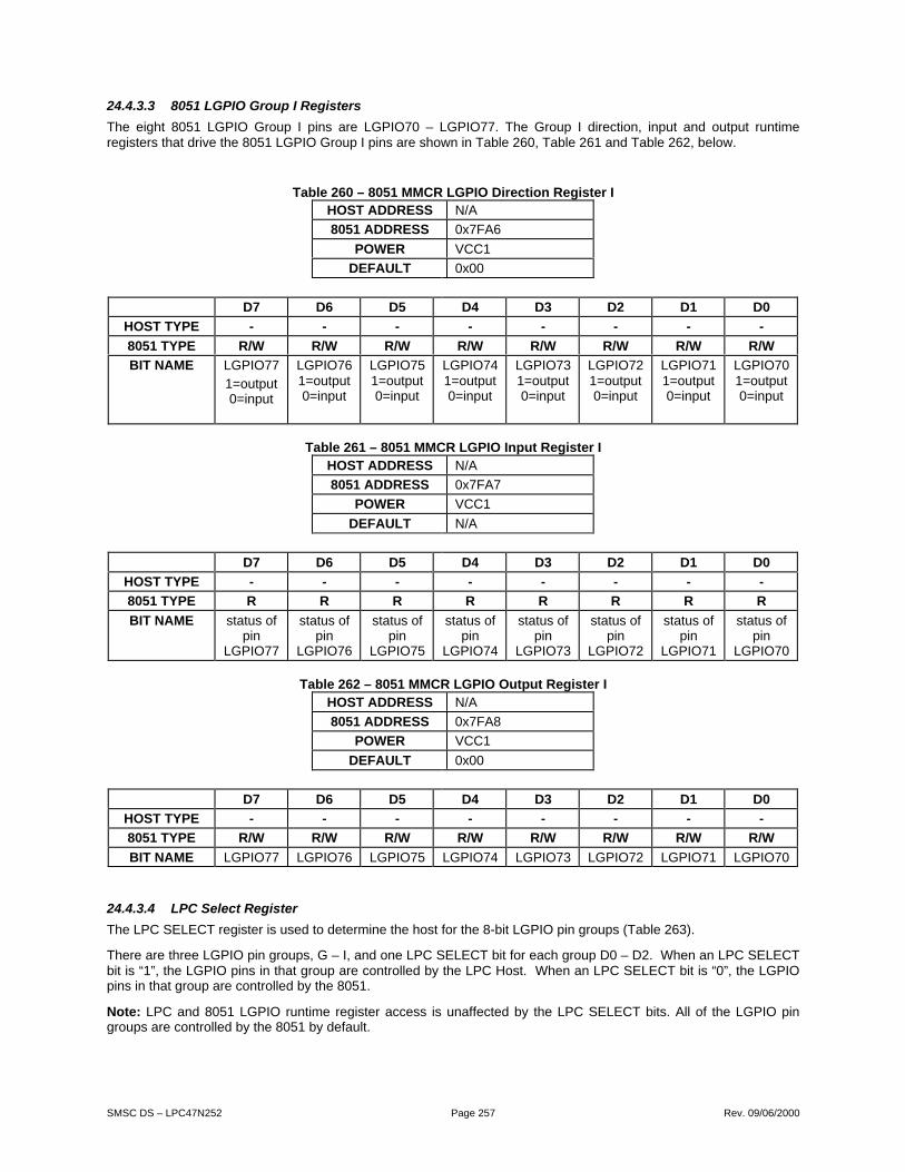
SMSC DS – LPC47N252 Page 257 Rev. 09/06/2000
24.4.3.3 8051 LGPIO Group I Registers
The eight 8051 LGPIO Group I pins are LGPIO70 – LGPIO77. The Group I direction, input and output runtimeregisters that drive the 8051 LGPIO Group I pins are shown in Table 260, Table 261 and Table 262, below.
Table 260 – 8051 MMCR LGPIO Direction Register IHOST ADDRESS N/A
8051 ADDRESS 0x7FA6
POWER VCC1
DEFAULT 0x00
D7 D6 D5 D4 D3 D2 D1 D0
HOST TYPE - - - - - - - -
8051 TYPE R/W R/W R/W R/W R/W R/W R/W R/W
BIT NAME LGPIO77
1=output0=input
LGPIO761=output0=input
LGPIO751=output0=input
LGPIO741=output0=input
LGPIO731=output0=input
LGPIO721=output0=input
LGPIO711=output0=input
LGPIO701=output0=input
Table 261 – 8051 MMCR LGPIO Input Register IHOST ADDRESS N/A
8051 ADDRESS 0x7FA7
POWER VCC1
DEFAULT N/A
D7 D6 D5 D4 D3 D2 D1 D0
HOST TYPE - - - - - - - -
8051 TYPE R R R R R R R R
BIT NAME status ofpin
LGPIO77
status ofpin
LGPIO76
status ofpin
LGPIO75
status ofpin
LGPIO74
status ofpin
LGPIO73
status ofpin
LGPIO72
status ofpin
LGPIO71
status ofpin
LGPIO70
Table 262 – 8051 MMCR LGPIO Output Register IHOST ADDRESS N/A
8051 ADDRESS 0x7FA8
POWER VCC1
DEFAULT 0x00
D7 D6 D5 D4 D3 D2 D1 D0
HOST TYPE - - - - - - - -
8051 TYPE R/W R/W R/W R/W R/W R/W R/W R/W
BIT NAME LGPIO77 LGPIO76 LGPIO75 LGPIO74 LGPIO73 LGPIO72 LGPIO71 LGPIO70
24.4.3.4 LPC Select Register
The LPC SELECT register is used to determine the host for the 8-bit LGPIO pin groups (Table 263).
There are three LGPIO pin groups, G – I, and one LPC SELECT bit for each group D0 – D2. When an LPC SELECTbit is “1”, the LGPIO pins in that group are controlled by the LPC Host. When an LPC SELECT bit is “0”, the LGPIOpins in that group are controlled by the 8051.
Note: LPC and 8051 LGPIO runtime register access is unaffected by the LPC SELECT bits. All of the LGPIO pingroups are controlled by the 8051 by default.
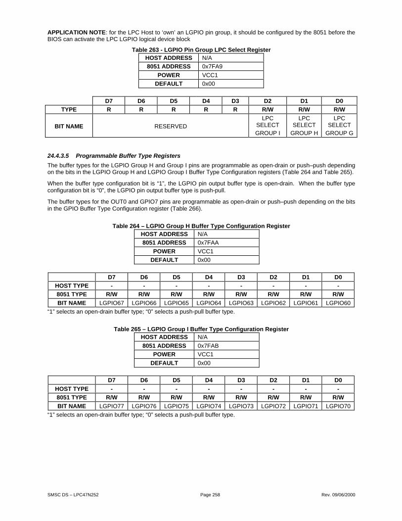
SMSC DS – LPC47N252 Page 258 Rev. 09/06/2000
APPLICATION NOTE: for the LPC Host to ‘own’ an LGPIO pin group, it should be configured by the 8051 before theBIOS can activate the LPC LGPIO logical device block
Table 263 - LGPIO Pin Group LPC Select RegisterHOST ADDRESS N/A
8051 ADDRESS 0x7FA9
POWER VCC1
DEFAULT 0x00
D7 D6 D5 D4 D3 D2 D1 D0
TYPE R R R R R R/W R/W R/W
BIT NAME RESERVEDLPC
SELECTGROUP I
LPCSELECT
GROUP H
LPCSELECT
GROUP G
24.4.3.5 Programmable Buffer Type Registers
The buffer types for the LGPIO Group H and Group I pins are programmable as open-drain or push–push dependingon the bits in the LGPIO Group H and LGPIO Group I Buffer Type Configuration registers (Table 264 and Table 265).
When the buffer type configuration bit is “1”, the LGPIO pin output buffer type is open-drain. When the buffer typeconfiguration bit is “0”, the LGPIO pin output buffer type is push-pull.
The buffer types for the OUT0 and GPIO7 pins are programmable as open-drain or push–push depending on the bitsin the GPIO Buffer Type Configuration register (Table 266).
Table 264 – LGPIO Group H Buffer Type Configuration RegisterHOST ADDRESS N/A
8051 ADDRESS 0x7FAA
POWER VCC1
DEFAULT 0x00
D7 D6 D5 D4 D3 D2 D1 D0
HOST TYPE - - - - - - - -
8051 TYPE R/W R/W R/W R/W R/W R/W R/W R/W
BIT NAME LGPIO67 LGPIO66 LGPIO65 LGPIO64 LGPIO63 LGPIO62 LGPIO61 LGPIO60
“1” selects an open-drain buffer type; “0” selects a push-pull buffer type.
Table 265 – LGPIO Group I Buffer Type Configuration RegisterHOST ADDRESS N/A
8051 ADDRESS 0x7FAB
POWER VCC1
DEFAULT 0x00
D7 D6 D5 D4 D3 D2 D1 D0
HOST TYPE - - - - - - - -
8051 TYPE R/W R/W R/W R/W R/W R/W R/W R/W
BIT NAME LGPIO77 LGPIO76 LGPIO75 LGPIO74 LGPIO73 LGPIO72 LGPIO71 LGPIO70
“1” selects an open-drain buffer type; “0” selects a push-pull buffer type.
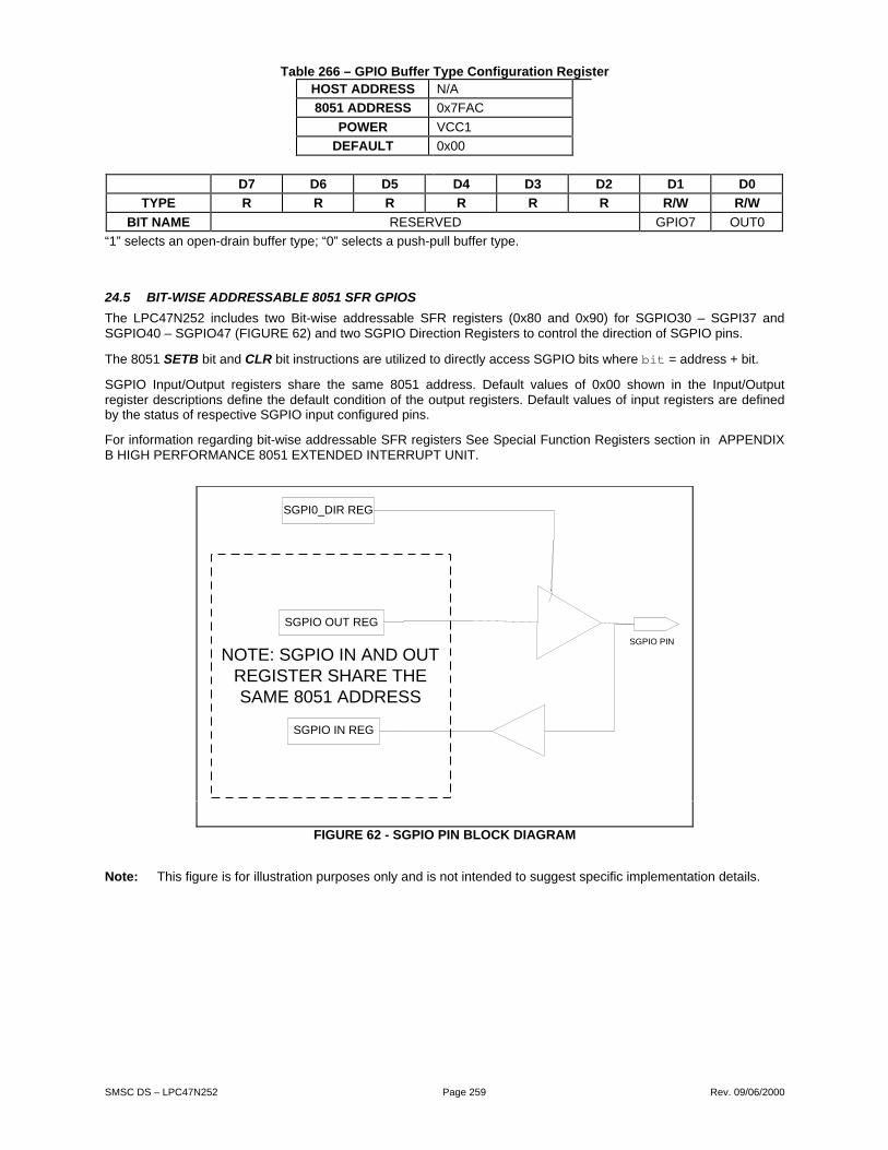
SMSC DS – LPC47N252 Page 259 Rev. 09/06/2000
Table 266 – GPIO Buffer Type Configuration RegisterHOST ADDRESS N/A
8051 ADDRESS 0x7FAC
POWER VCC1
DEFAULT 0x00
D7 D6 D5 D4 D3 D2 D1 D0
TYPE R R R R R R R/W R/W
BIT NAME RESERVED GPIO7 OUT0
“1” selects an open-drain buffer type; “0” selects a push-pull buffer type.
24.5 BIT-WISE ADDRESSABLE 8051 SFR GPIOS
The LPC47N252 includes two Bit-wise addressable SFR registers (0x80 and 0x90) for SGPIO30 – SGPI37 andSGPIO40 – SGPIO47 (FIGURE 62) and two SGPIO Direction Registers to control the direction of SGPIO pins.
The 8051 SETB bit and CLR bit instructions are utilized to directly access SGPIO bits where bit = address + bit.
SGPIO Input/Output registers share the same 8051 address. Default values of 0x00 shown in the Input/Outputregister descriptions define the default condition of the output registers. Default values of input registers are definedby the status of respective SGPIO input configured pins.
For information regarding bit-wise addressable SFR registers See Special Function Registers section in APPENDIXB HIGH PERFORMANCE 8051 EXTENDED INTERRUPT UNIT.
FIGURE 62 - SGPIO PIN BLOCK DIAGRAM
Note: This figure is for illustration purposes only and is not intended to suggest specific implementation details.
NOTE: SGPIO IN AND OUTREGISTER SHARE THESAME 8051 ADDRESS
SGPIO OUT REG
SGPIO PIN
SGPI0_DIR REG
SGPIO IN REG
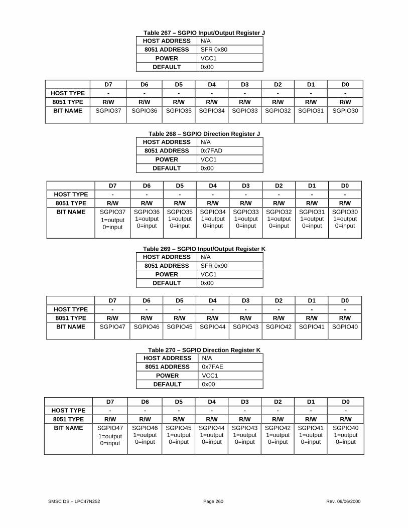
SMSC DS – LPC47N252 Page 260 Rev. 09/06/2000
Table 267 – SGPIO Input/Output Register JHOST ADDRESS N/A
8051 ADDRESS SFR 0x80
POWER VCC1
DEFAULT 0x00
D7 D6 D5 D4 D3 D2 D1 D0
HOST TYPE - - - - - - - -
8051 TYPE R/W R/W R/W R/W R/W R/W R/W R/W
BIT NAME SGPIO37 SGPIO36 SGPIO35 SGPIO34 SGPIO33 SGPIO32 SGPIO31 SGPIO30
Table 268 – SGPIO Direction Register JHOST ADDRESS N/A
8051 ADDRESS 0x7FAD
POWER VCC1
DEFAULT 0x00
D7 D6 D5 D4 D3 D2 D1 D0
HOST TYPE - - - - - - - -
8051 TYPE R/W R/W R/W R/W R/W R/W R/W R/W
BIT NAME SGPIO371=output0=input
SGPIO361=output0=input
SGPIO351=output0=input
SGPIO341=output0=input
SGPIO331=output0=input
SGPIO321=output0=input
SGPIO311=output0=input
SGPIO301=output0=input
Table 269 – SGPIO Input/Output Register KHOST ADDRESS N/A
8051 ADDRESS SFR 0x90
POWER VCC1
DEFAULT 0x00
D7 D6 D5 D4 D3 D2 D1 D0
HOST TYPE - - - - - - - -
8051 TYPE R/W R/W R/W R/W R/W R/W R/W R/W
BIT NAME SGPIO47 SGPIO46 SGPIO45 SGPIO44 SGPIO43 SGPIO42 SGPIO41 SGPIO40
Table 270 – SGPIO Direction Register KHOST ADDRESS N/A
8051 ADDRESS 0x7FAE
POWER VCC1
DEFAULT 0x00
D7 D6 D5 D4 D3 D2 D1 D0
HOST TYPE - - - - - - - -
8051 TYPE R/W R/W R/W R/W R/W R/W R/W R/W
BIT NAME SGPIO47
1=output0=input
SGPIO461=output0=input
SGPIO451=output0=input
SGPIO441=output0=input
SGPIO431=output0=input
SGPIO421=output0=input
SGPIO411=output0=input
SGPIO401=output0=input

SMSC DS – LPC47N252 Page 261 Rev. 09/06/2000
24.6 GPIO PASS-THROUGH PORTS
The LPC47N252 includes eight GPIO Pass-Through Ports. A GPIO Pass-Through Port multiplexes two generalpurpose I/O pins as shown in FIGURE 63. The GPIO Pass-Through Port (GPTP) can connect either the GPIOm pinor GPIOn to the GPIOn pin. The GPTPs are controlled by the PTMUX bits found in the GPIO Pass-Through Port Muxregister (see section 24.6.1 GPIO Pass-Through Port Mux Register). The eight GPTPs and their related PTMUX bitsare shown below in Table 271.
Note: This figure is for illustration purposes only and is not intended to suggest specific implementation details.
The eight GPIO Pass-Through Port multiplex LGPIO Group G (see section 24.4.3.1) with LGPIO Group H (seesection 24.4.2.2.)
Table 271 - Eight Kahuna GPIO Pass-Through Ports
GPIO PAIR (see Note 58)
GPIOm (see Note 60) GPIOn
MUXCONTROL
(see Note 59)
1. LGPIO50 LGPIO60 PTMUX1
2. LGPIO51 LGPIO61 PTMUX2
3. LGPIO52 LGPIO62 PTMUX3
4. LGPIO53 LGPIO63 PTMUX4
5. LGPIO54 LGPIO64 PTMUX5
6. LGPIO55 LGPIO65 PTMUX6
7. LGPIO56 LGPIO66 PTMUX7
8. LGPIO57 LGPIO67 PTMUX8
Note 58: See FIGURE 63 - GPIO PASS-THROUGH PORT.
Note 59: See Table 272 – GPIO Pass-Through Port Mux (GPTM) Register.
Note 60: These pins can generate 8051 interrupts and wake (See FIGURE 14, FIGURE 15, Table 118, and Table125 in section 11.9, 8051 Interrupts, which starts on page 136).
24.6.1 GPIO PASS-THROUGH PORT MUX REGISTER
The GPIO Pass-Through Port Mux Register contains the eight PTMUX bits that are used to control the Kahuna GPIOPass-Through Ports (Table 272). When a PTMUX bit is ‘0’ (default), the pass-through mode is disabled and theGPIO pins function normally. When a PTMUX bit is ‘1’, the pass-through mode is enabled, GPIOn (FIGURE 63) isdisconnected and the signal at the GPIOm pin appears unmodified at the GPIOn pin (see section 24.6.2 GPTPMultiplexer, below).
The GPTM register is powered by VCC1 and is controlled solely by the 8051.
MUX
GPIOm GPIOnGPIOm PIN
GPIOn PIN
PTMUXn
0
1
FIGURE 63 - GPIO PASS-THROUGH PORT

SMSC DS – LPC47N252 Page 262 Rev. 09/06/2000
Table 272 – GPIO Pass-Through Port Mux (GPTM) RegisterHOST ADDRESS N/A
8051 ADDRESS 0x7F85
POWER VCC1
DEFAULT 0x00
D7 D6 D5 D4 D3 D2 D1 D0
HOST TYPE - - - - - - - -
8051 TYPE R/W R/W R/W R/W R/W R/W R/W R/W
BIT NAME PTMUX8 PTMUX7 PTMUX6 PTMUX5 PTMUX4 PTMUX3 PTMUX2 PTMUX1
24.6.2 GPTP MULTIPLEXER
The GPIO Pass-Through Port Multiplexer determines connectivity for GPIOn PIN as shown in FIGURE 63. GPIOnPIN can be either an input or an output depending on the state of the PTMUX bit and the GPIOn direction register. InPass-Through mode, GPIOn PIN is always an output. In Normal mode, the GPIOn PIN direction depends upon theGPIOn Direction register (Table 273).
Table 273 - GPTP Multiplexer Direction ControlsGPIOm
DIRECTIONGPIOn
DIRECTION PTMUXGPIOn PIN
TYPEDESCRIPTION
IN X 1
OUT X 1
OUTPUTSee Note 60
PASS-THROUGHMODE
X IN 0 INPUT
X OUT 0 OUTPUT
NORMAL (GPIO)MODE
Note 61: When Pass through Mode is enabled, the GPIOn PIN TYPE is disconected from the GPIOn registers andthe GPIOm pin signal appears on GPIOn pin. The GPIOn 8051 LGPIO input register does not reflect the state of theGPIOn pin. This is the Pass Through Mode exception to Note 57.

SMSC DS – LPC47N252 Page 263 Rev. 09/06/2000
25 MULTIFUNCTION PIN
25.1 OVERVIEW
Many of the LPC47N252’s signal pins provide alternate functions which may be enabled by the 8051 firmware basedon the system design requirements. See Table 4 - Alternate Function Pinson page 15 for a complete list of all of themultifunction pins. The 8051 firmware controls the multiplexing functions for each of the multiplexed pins through theregisters described in this section. See the sub-sections that follow for a description of all of the MISC bits in theMultiplexing_1, Multiplexing_2, and Multiplexing_3 registers.
In Kahuna the KBD Scan Interface Pins are multiplexed to support the 8051 Flash Interface. The multiplex functionsfor these pins are not controlled by the 8051. For information about the multiplexed KBD Scan Interface Pins seesection 13.6 ATE Flash Program Access on page 172 and section 13.7 External Flash Interface on page 175.
25.2 FUNCTIONS AVAILABLE ON MORE THAN ONE PIN
The KBRST function can be made available on three pins: OUT8, KSO12 and OUT5. The OUT8 function can bemade available on two pins OUT8 and KSO12. The multiplex controls for these functions are described below. TheOUT8, KSO12, KSO13 and GPIO17 pin functions all depend on the MISC17 and MISC6 multiplex control bits (Table274). Note that OUT8 and KBRST cannot simultaneously exist on pins OUT8 and KS012 (FIGURE 64).
Table 274 - Multiplexing Register Bits Misc17 and Misc6MISC BITS PHYSICAL PINS
17 6 OUT8 KSO12 KSO13 GPIO170 0 OUT8 KSO12 KSO13 GPIO170 1 KBRST KSO12 KSO13 GATEA201 0 OUT8 OUT8 GPIO18 GPIO171 1 KBRST KBRST GPIO18 GATEA20
Note: see section 25.3
MISC6 – D6 on page 264 and section 0 MISC17 – D1 on page 269.
Table 275 - Multiplexing Register Bits Misc5 and Misc22MISC BITS PHYSICAL PINS
5 22 OUT5 OUT6
1 X nDS1 nMTR1
0 0 OUT5 OUT6
0 1 KBRST OUT6
Note: see section 0 MISC5 – D5 on page 264 and section 0 MISC 22 – D6. 0
FIGURE 64 - OUT8 AND KSO12 ALTERNATE FUNCTION OPERATION
1
0OUT8
MISC6
CPU_RESET
MISC17
KSO12
OUT8
1
0
KSO12
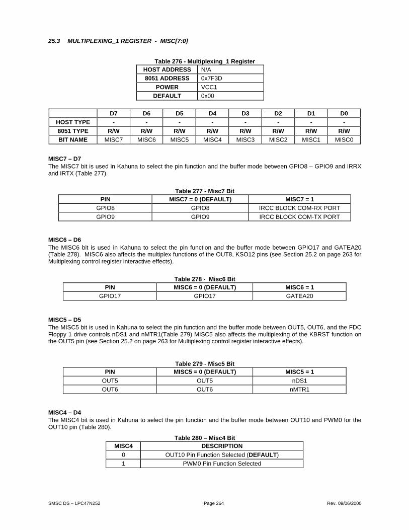
SMSC DS – LPC47N252 Page 264 Rev. 09/06/2000
25.3 MULTIPLEXING_1 REGISTER - MISC[7:0]
Table 276 - Multiplexing_1 RegisterHOST ADDRESS N/A
8051 ADDRESS 0x7F3D
POWER VCC1
DEFAULT 0x00
D7 D6 D5 D4 D3 D2 D1 D0
HOST TYPE - - - - - - - -
8051 TYPE R/W R/W R/W R/W R/W R/W R/W R/W
BIT NAME MISC7 MISC6 MISC5 MISC4 MISC3 MISC2 MISC1 MISC0
MISC7 – D7The MISC7 bit is used in Kahuna to select the pin function and the buffer mode between GPIO8 – GPIO9 and IRRXand IRTX (Table 277).
Table 277 - Misc7 BitPIN MISC7 = 0 (DEFAULT) MISC7 = 1
GPIO8 GPIO8 IRCC BLOCK COM-RX PORT
GPIO9 GPIO9 IRCC BLOCK COM-TX PORT
MISC6 – D6The MISC6 bit is used in Kahuna to select the pin function and the buffer mode between GPIO17 and GATEA20(Table 278). MISC6 also affects the multiplex functions of the OUT8, KSO12 pins (see Section 25.2 on page 263 forMultiplexing control register interactive effects).
Table 278 - Misc6 BitPIN MISC6 = 0 (DEFAULT) MISC6 = 1
GPIO17 GPIO17 GATEA20
MISC5 – D5The MISC5 bit is used in Kahuna to select the pin function and the buffer mode between OUT5, OUT6, and the FDCFloppy 1 drive controls nDS1 and nMTR1(Table 279) MISC5 also affects the multiplexing of the KBRST function onthe OUT5 pin (see Section 25.2 on page 263 for Multiplexing control register interactive effects).
Table 279 - Misc5 BitPIN MISC5 = 0 (DEFAULT) MISC5 = 1
OUT5 OUT5 nDS1
OUT6 OUT6 nMTR1
MISC4 – D4The MISC4 bit is used in Kahuna to select the pin function and the buffer mode between OUT10 and PWM0 for theOUT10 pin (Table 280).
Table 280 – Misc4 BitMISC4 DESCRIPTION
0 OUT10 Pin Function Selected (DEFAULT)
1 PWM0 Pin Function Selected

SMSC DS – LPC47N252 Page 265 Rev. 09/06/2000
MISC[3,1] – D3 and D1The MISC3 bit, along with the MISC1 bit, is used in Kahuna to select the pin function and the buffer mode betweenGPIO20 and GPIO21, the 8051 UART RX and TX, and the PS/2 CLK and DATA (Table 281).
Table 281 - Misc3 And Misc1 BitsMISC[3,1] PIN GPIO20 PIN GPIO21
[0,0] (DEFAULT) GPIO20 + 8051_RX * GPIO21
[0,1] PS2CLK PS2DAT
[1,0] GPIO20 + 8051_RX * 8051_TX **
[1,1] PS2CLK PS2DAT* GPIO20_DIR bit should be set to 0 when operating as an 8051_RX pin.** GPIO21_DIR bit must be set to 1 when operating as an 8051_TX pin.
The PS/2 pins on GPIO20 and GPIO21 are disabled (internally pulled high) when the non-PS/2 alternate functionsare selected. The PS/2 inputs under this condition are seen as a high to the PS/2 Device Interface logic.
Whenever a PS/2 channel is not enabled, the input signals to that channel must be high. Kahuna provides thisthrough the use of weak pull-ups since the EM and KB channels share a common receive path and the IM and PS2channels also share a common receive path.
FIGURE 65 - GPIO20 ALTERNATE FUNCTION STRUCTURE
FIGURE 66 - GPIO21 ALTERNATE FUNCTION STRUCTURE
1
0
GPIO20
GPIO20_DIR
MISC1
PS2_CLK_OUT
GPIO20_OUT
GPIO20_IN
PS2_CLK_IN
8051_RX
1
0 GPIO21
MISC1
MISC3
8051_TX
GPIO21_OUT
GPIO21_IN
PS2_DAT_IN
0
1PS2_DAT_OUT
GPIO21_DIR

SMSC DS – LPC47N252 Page 266 Rev. 09/06/2000
MISC2 – D2The MISC2 bit is used in Kahuna to select use of the IRCC Block and the IR DATA Register.
Table 282 - Misc2 BitPIN MISC2 = 0 (DEFAULT) MISC2 = 1
IRTX FROM IRCC BLOCK FROM IR DATA REGISTER
IRRX FROM IRCC BLOCK FROM IR DATA REGISTER
MISC0 – D0The MISC0 bit is used in Kahuna to select the pin function and the buffer mode between OUT1 andnIRQ8 (Table 283)
Table 283 - Misc0 BitMISC0 DESCRIPTION
0 OUT1 Pin Function Selected (DEFAULT)
1 nIRQ8 Pin Function Selected
25.4 MULTIPLEXING_2 REGISTER - MISC[16:9]
Table 284 - Multiplexing_2 RegisterHOST ADDRESS N/A
8051 ADDRESS 0x7F40
POWER VCC1
DEFAULT 0x00
D7 D6 D5 D4 D3 D2 D1 D0
HOST TYPE - - - - - - - -
8051 TYPE R/W R/W R/W R/W R/W R/W R/W R/W
BIT NAME MISC16 MISC15 MISC14 MISC13 MISC12 MISC11 RESERVED MISC9
MISC[16:15], D7 – D6The MISC16 and MISC15 bits are used in Kahuna to select the pin function and the buffer mode between GPIO6 andthe IrCC 2.0 IRMODE and IRRX3 functions (Table 285).
Table 285 – Misc[16:15] BitsMISC[16:15] PIN GPIO6
[0:0] (DEFAULT) GPIO10
[0:1] IR_MODE
(IRCC GP DATA) OUTPUT
[1:0] IRRX3 INPUT
[1:1] RESERVED
Note 62: The function of the GPIO10 pin is RESERVED when MISC[16:15] = 1,1 (Table 285).
MISC[14:13], D5 – D4The MISC14 and MISC13 bits are used in Kahuna to select the pin function and the buffer mode between GPIO6 andthe IrCC 2.0 IRMODE and IRRX3 functions (Table 286).

SMSC DS – LPC47N252 Page 267 Rev. 09/06/2000
Table 286 - Misc14 And Misc13 BitsMISC[14:13] PIN GPIO6
[0:0] (DEFAULT) GPIO6
[0:1] IR_MODE(IRCC GP DATA) OUTPUT
[1:0] IRRX3 INPUT
[1:1] RESERVED
Note 63: The function of the GPIO6 pin is RESERVED when MISC[14:13] = 1,1 (Table 286).
MISC12 – D3The MISC12 bit is used in Kahuna to select the pin function and buffer mode between OUT11 and PWM1 for theOUT11 pin (Table 287).
Table 287 – Misc12 BitMISC12 DESCRIPTION
0 OUT11 Pin Function Selected (DEFAULT)
1 PWM1 Pin Function Selected
MISC11The MISC11 bit is used in Kahuna to select the pin function and the buffer mode between OUT9 and PWM0 for theOUT9 pin (Table 288).
Table 288 - Misc11 BitMISC4 DESCRIPTION
0 OUT9 Pin Function Selected (DEFAULT)
1 PWM2 Pin Function Selected
MISC10The MISC10 bit is reserved
MISC9The MISC9 bit is used in Kahuna to select the between GPIO and Keyboard Scan Output alternate function and thebuffer modes for the GPIO4 and GPIO5 pins (Table 289).
Table 289 - Misc9 BitMISC9 PIN GPIO4 GPIO5
0 (DEFAULT) GPIO4 GPIO5
1 KSO14 KSO15
Note: When the KSO14 and KSO15 functions are enabled, the direction bits for GPIO4 and GPIO5 in 8051 MMCR0x7F18 have to be set to '1' for the KSO14 and KSO15 pins to function normally. When the KSO14 and KSO15functions are enabled and the GPIO[5:4] direction bits are set to '0', the KSO14 and KSO15 output drivers aredisabled; i.e., the KSO14 and KSO15 pins are inputs.
25.5 MULTIPLEXING_3 REGISTER - MISC[23:17]
Table 290 – Multiplexing_3 RegisterHOST ADDRESS N/A
8051 ADDRESS 0x7F30
POWER VCC1
DEFAULT 0x00
D7 D6 D5 D4 D3 D2 D1 D0
HOST TYPE - - - - - - - -
8051 TYPE R/W R/W R/W R/W R/W R/W R/W R/W
BIT NAME MISC23 MISC22 MISC21 MISC20 MISC19 MISC18 MISC17 RESERVED

SMSC DS – LPC47N252 Page 268 Rev. 09/06/2000
MISC23 – D7The MISC23 bit is used to select the pin function and the buffer mode between GPIO15 and FAN_TACH1 for theGPIO15 pin (Table 291).
Table 291 - Misc23 BitMISC23 DESCRIPTION
0 GPIO15 Function Selected (DEFAULT)
1 FAN_TACH1 Function Selected
MISC22 – D6The MISC22 bit is used along with the MISC5 bit in Multiplexing_1 register to select the KBRST alternate function #2of the OUT5 pin (Table 292). See Section 25.2 on page 263 for Multiplexing control register interactive effects.
Table 292 - Misc22 BitMISC5 MISC22 DESCRIPTION
1 X nDS1 Pin Function Selected.
0 0 OUT5 Pin Function Selected (DEFAULT)
0 1 KBRST Pin Function Selected
MISC21 – D5The MISC21 bit is used to select the pin function and the buffer mode between GPIO16 and FAN_TACH2 for theGPIO16 pin (Table 293).
Table 293 - Misc21 BitMISC23 DESCRIPTION
0 GPIO16 Function Selected (DEFAULT)
1 FAN_TACH2 Function Selected
MISC[20:19] D4 – D3The MISC20 and MISC19 bits are used to select the pin function and the buffer mode between the switchedACCESS.Bus 2 interface and the GPIO11, GPIO12, GPIO13 and GPIO14 pins. The MISC20 and MISC19 bits controlthe number of pins allocated for ACCESS.Bus 2 interface alternate functions as follows: ACCESS.Bus 2 interface (4pins), unswitched ACCESS.Bus 2 interface (2 pins), or no ACCESS.Bus 2 interface (0 pins). Pins not allocated tothe ACCESS.Bus 2 interface are allocated to GPIO interface.
Table 294 - Misc[20:19] BitsMISC19 MISC20 PIN GPIO11 PIN GPIO12 PIN GPIO13 PIN GPIO14 DESCRIPTION
0 0 GPIO11 GPIO12 GPIO13 GPIO14 Four GPIO pins(Default)
0 1 AB2A_DATA AB2A_CLK GPIO13 GPIO14 SwitchedAccess.Bus2 andTwo GPIO pins
1 0 AB2A_DATA AB2A_CLK AB2B_DATA AB2B_CLK SwitchedAccess.Bus 2
1 1 Reserved
Note 64: The function of the GPIO10 pin is RESERVED when MISC[20:19] = 1,1 (Table 294).
Note 65: When the Access Bus 2 function is enabled, the direction bits for GPIO11, GPIO12, GPIO13 and GPIO14 in8051 MMCR 0x7F1B have to be set as outputs for the Access Bus 2 pins to function normally. Access Bus 2 is thealternate function for these pins. When the Access Bus 2 function is enabled and the GPIO[11:14] direction bits areset as inputs, the Access Bus 2 controller can monitor, but not drive, the Access Bus 2 Clock and Data pins.
MISC18 – D2The MISC18 bit is used in Kahuna, along with bit D3 in the ESMI Mask register to select the pin function and buffermode for the OUT7 pin and the SMI transfer mechanism to the host. (Table 295). When MISC18 = ‘0’, the primaryfunction of the OUT7 pin is selected and the SMI is routed to the Serial IRQ interface. If the SMI is masked, SIRQslot3 is available as IRQ2. When MISC18 = ‘1’, the alternate nSMI function of the OUT7 pin is selected, the pad is

SMSC DS – LPC47N252 Page 269 Rev. 09/06/2000
driven open-drain, and the Serial IRQ slot3 is available as IRQ2. The ESMI Mask register IS MBX97h. See Section19.7, ESMI REGISTERS on page 228.
Table 295 – Misc18 And Esmi Mask BitsESMI MASKREGISTER
FUNCTION
D3
MISC18
OUT7 PIN SIRQ SLOT3
DESCRIPTION
0 0 OUT7 nSMI SERIAL SMI (DEFAULT)
0 1 nSMI IRQ2 PARALLEL SMI, SERIAL IRQIRQ2 AVAILABLE
1 0 OUT7 IRQ2 MASKED SERIAL SMI, IRQ2AVAILABLE
1 1 nSMI IRQ2 PARALLEL SMI MASKED(INACTIVE), IRQ2 AVAILABLE
MISC17 – D1The MISC17 bit is used in Kahuna to select the pin function and buffer mode between KSO13 and GPIO18 on pinKSO13 (Table 296). MISC17 also affects the multiplex functions for the OUT8, KSO12 and KSO13 pins (see Section25.2 on page 263 for Multiplexing control register interactive effects).
The MISC17 bit is used in the LPC47N252 to select the pin function and buffer mode between GPIO18 and nDACK2on pin GPIO18 and between KSO13 and GPIO18 on pin KSO13.
Table 296 - Misc17MISC17 PIN KSO13
0 KSO13
1 GPIO18
MISC8 – D0The MISC8 bit is RESERVED.

SMSC DS – LPC47N252 Page 270 Rev. 09/06/2000
26 ACPI PM1 BLOCK
26.1 ACPI PM1 BLOCK OVERVIEW
The LPC47N252 supports ACPI as described in this section. These features comply with the ACPI Specification,Revision 1.0, through a combination of hardware and 8051 software.
The LPC47N252 implements the ACPI fixed registers but includes only those bits that apply to the power buttonsleep button and RTC alarm events. The ACPI WAK_STS, SLP_TYPx, and SLP_EN bits are also supported.
The registers in the LPC47N252 ACPI PM1 Block occupy eight addresses in the host I/O space and are specified asoffsets from the ACPI PM1 Block base address. The ACPI PM1 Block base address is relocatable depending on thevalues programmed in LPC47N252 configuration registers CR60 and CR61 in Logical Device Number 1.
The functions described in the following sub-sections can generate a SCI event on the nEC_SCI pin. In theLPC47N252, an SCI event is considered the same as an ACPI wakeup or runtime event. The 8051 can alsogenerate a SCI on the nEC_SCI pin by setting the 8051_SCI_STS bit in the 8051_PM_STS register (see nEC_SCIPin Interface).
26.2 ACPI PM1 BLOCK SCI EVENT-GENERATING FUNCTIONS
Power Button With OverrideThe power button has a status and an enable bit in the PM1_BLK of registers to provide an SCI upon the buttonpress. The status bit is software Read/Writeable by the 8051; the enable bit is Read-only by the 8051. It also has astatus and enable bit in the PM1_BLK of registers to indicate and control the power button override (fail-safe) event.These bits are not required by ACPI. The power button override event status bit is software Read/Writeable by the8051; the enable bit is software read-only by the 8051. The enable bit for the override event is located at bit 1 in thePM1_CNTRL2 register.
The power button enable bit is set by the Host to enable the generation of an SCI due to the power button event. Thestatus bit is set by the 8051 when it generates a power button event and is cleared by the Host writing a ‘1’ to this bit(writing a ‘0’ has no effect); it can also be cleared by the 8051. If the enable bit is set, the 8051 will generate an SCIpower management event.
Sleep ButtonThe sleep button has a status and an enable bit in the PM1_BLK of registers to provide an SCI upon the buttonpress. The status bit is software Read/Writeable by the 8051; the enable bit is Read-only by the 8051.
The sleep button enable bit is set by the Host to enable the generation of an SCI due to the sleep button event. Thestatus bit is set by the 8051 when it generates a sleep button event and is cleared by the Host writing a ‘1’ to this bit(writing a ‘0’ has no effect); it can also be cleared by the 8051. If the enable bit is set, the 8051 will generate an SCIpower management event.
RTC AlarmThe ACPI specification requires that the RTC alarm generate a hardware wake-up event from the sleeping state. TheRTC alarm can be enabled as an SCI event and its status can be determined through bits in the PM1_BLK ofregisters. The status bit is software Read/Writeable by the 8051; the enable bit is Read-only by the 8051.
The RTC enable bit is set by the Host to enable the generation of an SCI due to the RTC alarm event. The status bitis set by the 8051 when the RTC generates an alarm event and is cleared by the Host writing a ‘1’ to this bit (writing a‘0’ has no effect); it can also be cleared by the 8051. If the enable bit is set, the 8051 will generate an SCI powermanagement event.
26.3 ACPI PM1 BLOCK BASE ADDRESS
Logical Device 1 in the LPC47N252 configuration space supports the ACPI PM1 Block registers interface. Threedevice configuration registers in LDN1 provide activation control and the base address programming for the ACPIPM1 Block registers (Table 297). Register 0x30 is the Activate register. The activation control (LDN1:CR30.0)qualifies address decoding for the ACPI PM1 Block registers; e.g., if the Activate bit D0 in the Activate register is “0”,the PM1 Block addresses will not be decoded; if the Activate bit is “1”, PM1 Block addresses will be decodeddepending on the values programmed in the ACPI PM1 Block Primary Base Address registers. Registers 0x60 and0x61 are the ACPI PM1 Block Primary Base Address registers. Register 0x60 is the ACPI PM1 Block Primary BaseAddress High Byte, register 0x61 is the ACPI PM1 Block Primary Base Address Low Byte. Note: The ACPI PM1

SMSC DS – LPC47N252 Page 271 Rev. 09/06/2000
Block base address must be located on eight -byte boundaries; i.e., bits D0 – D2 in the ACPI PM1 Block PrimaryBase Address Low Byte must be “0”. Valid ACPI PM1 Block base address values are 0x0000 – 0x0FF8.
Table 297 – ACPI PM1 Bock Configuration Registers (LDN1)
INDEX TYPEHARDRESET
SOFTRESET
VCC2POR
VCC1&VCC0 POR
DESCRIPTION
D7 D6 D5 D4 D3 D2 D1 D0
0x30 R/W 0x00 0x00 0x00 - Activate
RESERVED Activate
0x60 R/W 0x00 0x00 0x00 - ACPI PM1 Block Primary Base Address High Byte
“0” “0” “0” “0” A11 A10 A9 A8
0x61 R/W 0x00 0x00 0x00 - ACPI PM1 Block Primary Base Address Low Byte
A7 A6 A5 A4 A3 “0” “0” “0”
26.4 ACPI PM1 BLOCK
DescriptionThe ACPI register model consists of a number of fixed register blocks that perform designated functions. A registerblock consists of a number of registers that perform Status, Enable and Control functions. The ACPI specificationdeals with events (which have an associated interrupt status and enable bits, and sometimes an associated controlfunction) and control features. The status registers illustrate what defined function is requesting ACPI interruptservices (SCI). Any status bit in the ACPI specification has the following attributes:
§ Status bits are only set through some defined hardware or 8051 event.§ Unless otherwise noted, Status bits are cleared by the system writing a “1” to that bit position, and upon VCC1
POR. Writing a ‘0’ has no effect.§ Status bits only generate interrupts while their associated bit in the enable register is set.§ Function bit positions in the status register have the same bit position in the enable register (there are exceptions
to this rule, special status bits have no enables).§ Note that this implies that if the respective enable bit is reset and the hardware event occurs, the respective
status bit is set; however no interrupt is generated until the enable bit is set. This allows software to test the stateof the event (by examining the status bit) without necessarily generating an interrupt. There are a special class ofstatus bits that have no respective enable bit, these are called out specifically, and the respective enable bit inthe enable register is marked as reserved for these special cases.
§ The enable registers allow the setting of the status bit to generate an interrupt (under 8051 control). As a generalrule there is an enable bit in the enable register for every status bit in the status register. The control registerprovides special controls for the associated event, or special control features that are not associated with aninterrupt event. The order of a register block is the status registers, followed by enable registers, followed bycontrol registers.
26.5 REGISTERS
The registers in the LPC47N252 ACPI PM1 Block occupy eight addresses in the host I/O space and are specified asoffsets from the ACPI PM1 Block base address (Table 298).
The registers in the PM1 Block are powered by VCC1.
Table 298 – ACPI PM1 Block Registers
REGISTER
SIZE
(bits) OFFSET
ADDRESS
PM1_STS 1 8 0 <ACPI PM1 Block Base Address>
PM1_STS 2 8 1 <ACPI PM1 Block Base Address>+1h
PM1_EN 1 8 2 <ACPI PM1 Block Base Address>+2h
PM1_EN 2 8 3 <ACPI PM1 Block Base Address>+3h
PM1_CNTRL 1 8 4 <ACPI PM1 Block Base Address>+4h
PM1_CNTRL 2 8 5 <ACPI PM1 Block Base Address>+5h
RESERVED 8 6 <ACPI PM1 Block Base Address>+6h
RESERVED 8 7 <ACPI PM1 Block Base Address>+7h

SMSC DS – LPC47N252 Page 272 Rev. 09/06/2000
26.5.1 POWER MANAGEMENT 1 STATUS REGISTER 1 (PM1_STS 1)
Host Register Location: <ACPI PM1 Block Base Address> System I/O Space8051 Register Location: n/aDefault Value: 00h on VCC1 PORHost Attribute: ReadSize: 8-bits
BIT NAME DESCRIPTION0-7 Reserved Reserved. These bits always return a value of zero.
26.5.2 POWER MANAGEMENT 1 STATUS REGISTER 2 (PM1_STS 2)
Host Register Location: <ACPI PM1 Block Base Address>+1h System I/O Space8051 Register Location: 0x7F80Default Value: 00h on VCC1 PORHost Attribute: Read/Write (Note 1)8051 Attribute Read/WriteSize: 8-bits
Note 1: These bits are set/cleared by the 8051 directly i.e., writing ‘1’ sets the bit and writing ‘0’ clears it. These bitscan also be cleared by the Host software writing a one to this bit position and by VCC1 POR. Writing a 0 by the Hosthas no effect.
An interrupt is generated to the 8051 when the Host writes to this register.
BIT NAME DESCRIPTION
0 PWRBTN_STS This bit can be set or cleared by the 8051 to simulate a Power button status if thepower is controlled by the 8051. The Host writing a one to this bit can also clearthis bit. The 8051 must generate the associated SCI interrupt under softwarecontrol.
1 SLPBTN_STS This bit can be set or cleared by the 8051 to simulate a Sleep button status if thesleep state is controlled by the 8051. The Host writing a one to this bit can alsoclear this bit. The 8051 must generate the associated SCI interrupt under softwarecontrol.
2 RTC_STS This bit can be set or cleared by the 8051 to simulate a RTC status. The Hostwriting a one to this bit can also clear this bit. The 8051 must generate theassociated SCI interrupt under software control.
3 PWRBTNOR_STS This bit can be set or cleared by the 8051 to simulate a Power button overrideevent status if the power is controlled by the 8051. The Host writing a one to thisbit can also clear this bit. The 8051 must generate the associated hardware eventunder software control.
4-6 Reserved Reserved. These bits always return a value of zero.
7 WAK_STS This bit can be set or cleared by the 8051. The Host writing a one to this bit canalso clear this bit.
26.5.3 POWER MANAGEMENT 1 ENABLE REGISTER 1 (PM1_EN 1)
Host Register Location: <ACPI PM1 Block Base Address>+2 System I/O Space8051 Register Location: n/aDefault Value: 00h on VCC1 PORHost Attribute: ReadSize: 8-bits
BIT NAME DESCRIPTION
0-7 Reserved Reserved. These bits always return a value of zero.
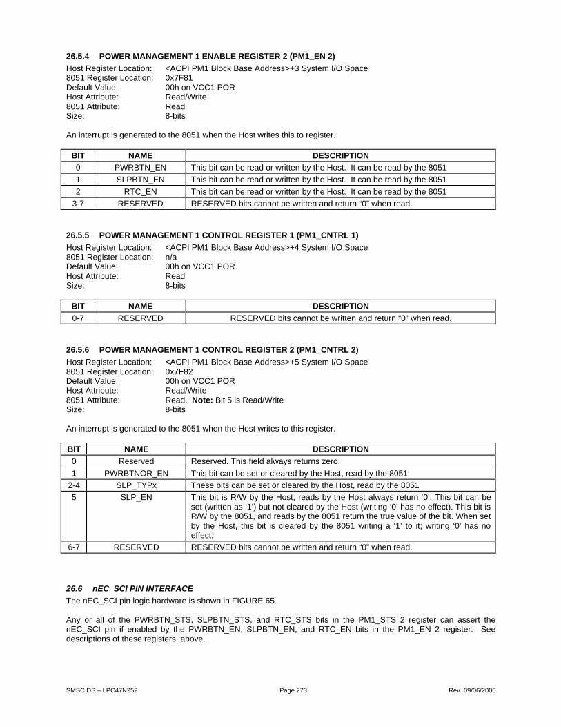
SMSC DS – LPC47N252 Page 273 Rev. 09/06/2000
26.5.4 POWER MANAGEMENT 1 ENABLE REGISTER 2 (PM1_EN 2)
Host Register Location: <ACPI PM1 Block Base Address>+3 System I/O Space8051 Register Location: 0x7F81Default Value: 00h on VCC1 PORHost Attribute: Read/Write8051 Attribute: ReadSize: 8-bits
An interrupt is generated to the 8051 when the Host writes this to register.
BIT NAME DESCRIPTION
0 PWRBTN_EN This bit can be read or written by the Host. It can be read by the 8051
1 SLPBTN_EN This bit can be read or written by the Host. It can be read by the 8051
2 RTC_EN This bit can be read or written by the Host. It can be read by the 8051
3-7 RESERVED RESERVED bits cannot be written and return “0” when read.
26.5.5 POWER MANAGEMENT 1 CONTROL REGISTER 1 (PM1_CNTRL 1)
Host Register Location: <ACPI PM1 Block Base Address>+4 System I/O Space8051 Register Location: n/aDefault Value: 00h on VCC1 PORHost Attribute: ReadSize: 8-bits
BIT NAME DESCRIPTION
0-7 RESERVED RESERVED bits cannot be written and return “0” when read.
26.5.6 POWER MANAGEMENT 1 CONTROL REGISTER 2 (PM1_CNTRL 2)
Host Register Location: <ACPI PM1 Block Base Address>+5 System I/O Space8051 Register Location: 0x7F82Default Value: 00h on VCC1 PORHost Attribute: Read/Write8051 Attribute: Read. Note: Bit 5 is Read/WriteSize: 8-bits
An interrupt is generated to the 8051 when the Host writes to this register.
BIT NAME DESCRIPTION
0 Reserved Reserved. This field always returns zero.
1 PWRBTNOR_EN This bit can be set or cleared by the Host, read by the 8051
2-4 SLP_TYPx These bits can be set or cleared by the Host, read by the 8051
5 SLP_EN This bit is R/W by the Host; reads by the Host always return ‘0’. This bit can beset (written as ‘1’) but not cleared by the Host (writing ‘0’ has no effect). This bit isR/W by the 8051, and reads by the 8051 return the true value of the bit. When setby the Host, this bit is cleared by the 8051 writing a ‘1’ to it; writing ‘0’ has noeffect.
6-7 RESERVED RESERVED bits cannot be written and return “0” when read.
26.6 nEC_SCI PIN INTERFACE
The nEC_SCI pin logic hardware is shown in FIGURE 65.
Any or all of the PWRBTN_STS, SLPBTN_STS, and RTC_STS bits in the PM1_STS 2 register can assert thenEC_SCI pin if enabled by the PWRBTN_EN, SLPBTN_EN, and RTC_EN bits in the PM1_EN 2 register. Seedescriptions of these registers, above.

SMSC DS – LPC47N252 Page 274 Rev. 09/06/2000
The 8051_SCI_STS bit can assert the nEC_SCI pin at any time, without being enabled. The 8051_SCI_STS bit islocated in the 8051_PM_STS register at MMCR address 0x7F83h (Table 299).
The 8051_SCI_STS bit is in the LPC47N252 and is read/write by the 8051. If the 8051_SCI_STS bit is “1”, aninterrupt is generated on the nEC_SCI pin.
PM1_EN 2Register
PM1_STS 2Register
PWRBTN_STS
SLPBTN_STS
RTC_STS
8051_SCI_STS
8051_PM_STS Register
nEC_SCI
FIGURE 67 – HARDWARE nEC_SCI INTERFACE
Table 299 – 8051_Pm_Sts RegisterHOST ADDRESS 8051 ADDRESS POWER PLANE DEFAULT
- 0x7F83 VCC1 0x00
D7 D6 D5 D4 D3 D2 D1 D0
HOST TYPE - - - - - - - -
8051 TYPE R R R R R R R R/W
BIT NAME RESERVED(RESERVED bits cannot be written and return “0” when read)
8051_SCI_STS

SMSC DS – LPC47N252 Page 275 Rev. 09/06/2000
27 REAL TIME CLOCK
27.1 GENERAL DESCRIPTION
The Real Time Clock Supercell (RTC) is a complete time of day clock with alarm, day of month alarm, one hundredyear calendar, a century byte, and a programmable periodic interrupt. The RTC address space consists of two-128bytes.banks of CMOS RAM (Bank0 and Bank1.) Each bank is accessable via address and data ports. These accessports have relocatable addresses and are acessable by both the host and the 8051. Each bank’s last addressablelocation accesses the Shared RTC Control. The remaining 127 bytes of Bank0 contain the following: eleven registersof time, calendar, century , and alarm data, four control and status registers, and 111 bytes of general purposeregisters. The remaining 127bytes of Bank1 contain general purpose registers.
Features:§ Allow 32kHz clock input or a 32kHz crystal.§ Counts seconds, minutes, and hours of the day.§ Counts days of the week, date, month and year.§ Binary or BCD representation of time, calendar and alarm.§ 24 hour daily alarm.§ 30-day alarm.§ RTC/CMOS Bank Addresses are relocatable.§ The RTC CMOS Bank0 index register (70h) is shadowed§ RTC Interrupt (IRQ8) is available on the parallel nIRQ8 pin.§ RTC power source is switched internally between the VCC1 and VCC0 pins according to VCC1_PWRGD (See
FIGURE 4 - VCC2 POWER-UP TIMING and FIGURE 5 - VCC1_PWRGD TIMING).§ Lockable CMOS Ram Address Ranges (See Table 322 - RTC, Logical DEVICE 6 [LOGICAL DEVICE NUMBER
= 0X06] in Section 31.10 SMSC Defined Logical Device Configuration Registers)
27.2 CONFIGURATION REGISTERS
The RTC configuration registers, in Logical Device Number 6, provide activation control and the base address for therun-time registers (See Table 300)
The activate bit register 0x30, Bit D0 enables RTC/CMOS Bank0.
The activate bit register 0x30, Bit D1 enables RTC/CMOS Bank1.
Table 300 - RTC Configuration RegistersDESCRIPTION
INDEX TYPEHARDRESET
SOFTRESET
VCC2POR
VCC1&VCC0POR
D7 D6 D5 D4 D3 D2 D1 D0
0x30 R/W 0x00 0x00 0x00 - Activate
RESERVED ActivateCMOSBank1
ActivateRTC/CMOSBank0
0x60 R/W 0x00 0x00 0x00 - RTC/CMOS Bank0 Primary Base Address High Byte
“0” “0” “0” “0” A11 A10 A9 A8
0x61 R/W 0x70 0x70 0x70 - RTC/CMOS Bank0 Primary Base Address Low Byte
A7 A6 A5 A4 A3 A2 A1 “0”
0x62 R/W 0x00 0x00 0x00 - CMOS Bank1 Primary Base Address High Byte
“0” “0” “0” “0” A11 A10 A9 A8
0x63 R/W 0x74 0x74 0x74 - CMOS Bank1 Primary Base Address Low Byte
A7 A6 A5 A4 A3 A2 A1 “0”
0xF1 R - - - - Shadow RTC/CMOS Bank 0 Index register
27.3 ISA HOST I/O INTERFACE
Each bank has a CMOS Address Register and a CMOS Data Register. Each bank’s CMOS Address Register islocated at the corresponding base address setup by the Configuration Registers in Table 300. Each bank’s CMOSData Register is located at an offest of the coresponding base (see TABLE 301.) Bit D7 of both CMOS AddressRegisters is not used for the CMOS RAM address decoding. All four CMOS Run Time regesters are fully read/write.

SMSC DS – LPC47N252 Page 276 Rev. 09/06/2000
Table 301 - CMOS Run Time RegistersH OST A DD RESS* B AN K F UN CT ION
Bank0 * (R /W) R TC /C M OS Bank0 C MOS Address Register
Bank0 * + 1(R /W ) R TC /C M OS Bank0 C MOS D ata R egister
Bank1 * (R /W) C MOS Bank1 C MOS Address Register
Bank1 * + 2(R /W ) C MOS Bank1 C MOS D ata R egister
27.4 INTERNAL REGISTERS
Table 302 shows the address map of the RTC and CMOS RAM, eleven registers of time, calendar, century , andalarm data, four control and status registers , 239 bytes of CMOS registers and one :Shared RTC Control register.Each bank’s last addressable location accesses the same reigister: Shared RTC Control.
Table 302 – RTC and CMOS RAM Address Map
BANKBASE
OFFEST REGISTER TYPE REGISTER FUNCTION
Bank0 0 R/W Register 0: Seconds
Bank0 1 R/W Register 1: Seconds Alarm
Bank0 2 R/W Register 2: Minutes
Bank0 3 R/W Register 3: Minutes Alarm
Bank0 4 R/W Register 4: Hours
Bank0 5 R/W Register 5: Hours Alarm
Bank0 6 R/W Register 6: Day of Week
Bank0 7 R/W Register 7: Day of Month
Bank0 8 R/W Register 8: Month
Bank0 9 R/W Register 9: Year
Bank0 A R/W Register A:
Bank0 B R/W Register B: (Bit 0 is ReadOnly)
Bank0 C R Register C:
Bank0 D R/W Register D:Day of Month Alarm
Bank0 32 R/W Century Byte
Bank0 E-31,33-7F
R/W General purpose
Bank0 7F R/W : Shared RTC Control
Bank1 0-7E R/W Bank 1: General purpose
Bank1 7F R/W : Shared RTC Control
All 256 bytes are directly writable and readable by the host with the following exceptions:
§ Registers C is read only§ Bit 7 of Register D is read only w hi ch can onl y be set by a r ead of R egister D .§ Bit 6 of Register D is read only .§ Bit 7 of Register A is read only§ Bits 0 of Register B is read only§ Bits 7-1 of the Shared RTC Control register are read only
27.5 TIME CALENDAR AND ALARM
The processor program obtains time and calendar information by reading the appropriate locations. The program mayinitialize the time, calendar and alarm by writing to these locations. The contents of the twelve time, calendar andalarm registers can be in binary or BCD as shown in Table 303 - RTC Register Valid Range.
Before initializing the internal registers, the SET bit in Register B should be set to a "1" to prevent time/calendarupdates from occurring. The program initializes the twelve locations in the binary or BCD format as defined by the DMbit in Register B. The SET bit may then be cleared to allow updates.

SMSC DS – LPC47N252 Page 277 Rev. 09/06/2000
The 12/24 bit in Register B establishes whether the hour locations represent 1 to 12 or 0 to 23. The 12/24 bit cannotbe changed without reinitializing the hour locations. When the 12 hour format is selected, the high order bit of thehours byte represents PM when it is a "1".
Once per second, the twelve time, calendar and alarm registers are updated, Incrementing by one second andchecking for an alarm condition. During the update cycle all the registers in Table 303 , except Register D, are notaccessible by the processor program. The update cycle time is shown in Table 301. The update logic containscircuitry for automatic end-of-month recognition as well as automatic leap year compensation.
The three alarm registers may be used in two ways. First, when the program inserts an alarm time in the appropriatehours, minutes and seconds alarm locations, the alarm interrupt is initiated at the specified time each day if the alarmenable bit is high. The second usage is to insert a "don't care” state in one or more of three alarms registers. The"don't care" code is any hexadecimal byte from C0 to FF inclusive. That is the two most significant bits of each byte,when set to "1" create a "don't care" situation. An alarm interrupt each hour is created with a "don't care" code in thehours alarm location. Similarly, an alarm is generated every minute with "don't care" codes in the hours and minutesalarm bytes. The "don't care" codes in all three alarm bytes create an interrupt every second.
Table 303 - RTC Register Valid Range
ADD REGISTER FUNCTIONBCD
RANGEBINARYRANGE
0 Register 0: Seconds 00-59 00-3B
1 Register 1: Seconds Alarm 00-59 00-3B
2 Register 2: Minutes 00-59 00-3B
3 Register 3: Minutes Alarm 00-59 00-3B
4 Register 4: Hours 01-12 am 01-0C
(12 hour mode) 81-92 pm 81-8C
(24 hour mode) 00-23 00-17
5 Register 5: Hours Alarm 01-12 am 01-0C
(12 hour mode) 81-92 pm 81-8C
(24 hour mode) 00-23 00-17
6 Register 6: Day of Week 01-07 01-07
7 Register 7: Day of Month 01-31 01-1F
8 Register 8: Month 01-12 01-0C
9 Register 9: Year 00-99 00-63
D Day of Month Alarm 01-31 01-1F
32 Century Byte 00-99 00-63
27.6 UPDATE CYCLE
An update cycle is executed once per second if the SET bit in Register B is clear and the DV0-DV2 divider is notclear. The SET bit in the "1" state permits the program to initialize the time and calendar registers by stopping anexisting update and preventing a new one from occurring.
The primary function of the update cycle is to increment the seconds register, check for overflow, increment theminutes register when appropriate and so forth through to the year of the century byte. The update cycle alsocompares each alarm register with the corresponding time register and issues an alarm if a match or if a "don't care"code is present.
The length of an update cycle is shown in Table 301. During the update cycle the time, calendar and alarm registersare not accessible by the processor program. If the processor reads these locations before the update cycle iscomplete the output will be undefined. The UIP (update in progress) status bit is set during the interval. When the UIPbit goes high, the update cycle will begin 244 µs later. Therefore, if a low is read on the UIP bit the user has at least244 µs before time/calendar data will be changed.

SMSC DS – LPC47N252 Page 278 Rev. 09/06/2000
Table 304 - RTC Update Cycle Timing
INPUT CLOCKFREQUENCY UIP BIT
UPDATE
CYCLE TIME
MINIMUM TIME BEFORESTART OF UPDATE
CYCLE
32.768 kHz 1 1948 µs -
32.768 KHZ 0 - 244 µs
27.7 CONTROL AND STATUS REGISTERS
The RTC has four registers, which are accessible to the processor program at all times, even during the update cycle.
27.7.1 REGISTER A
B7 B6 B5 B4 B3 B2 B1 B0
UIP DV2 DV1 DV0 RS3 RS2 RS1 RS0
UIPThe update in progress bit is a status flag that may be monitored by the program. When UIP is a "1" the update cycleis in progress or will soon begin. When UIP is a "0" the update cycle is not in progress and will not be for at least 244µs. The time, calendar, and alarm information is fully available to the program when the UIP bit is “0”. The UIP bit is aread only bit and is not affected by VCC1 POR. Writing the SET bit in Register B to a "1" inhibits any update cycleand then clears the UIP status bit.
DV2-0Three bits are used to permit the program to select various conditions of the 22 stage divider chain.TABLE 305 shows the allowable combinations. The divider selection bits are also used to reset the divider chain.When the time/calendar is first initialized, the program may start the divider chain at the precise time stored in theregisters. When the divider reset is removed the first update begins one-half second later. These three read/write bitsare not affected by VCC1 POR.
Table 305 - RTC Divider Selection BitsOSCILLATOR REGISTER A BITS
FREQUENCY DV2 DV1 DV0 MODE
1. 0 0 0 Normal Operation
2. 0 0 1 Reset Divider
3. 0 1 0 Normal Operation
4. 0 1 1 Oscillator Disabled
5. 1 0 X Test
6.
32.768 kHz
1 1 X Reset Divider
RS3-0The four rate selection bits select one of 15 taps on the divider chain or disable the divider output. The selected tapdetermines rate or frequency of the periodic interrupt. The program may enable or disable the interrupt with the PIEbit in Register B. Table 306 lists the periodic interrupt rates and equivalent output frequencies that may be chosenwith the RS0-RS3 bits. These four bits are read/write bits which are not affected by VCC1 POR.
Table 306 – RTC Periodic Interrupt RatesRATE SELECT 32.768 kHz TIME BASE
RS3 RS2 RS1 RS0 PERIOD RATEOF INTERRUPT
FREQUENCYOF INTERRUPT
0 0 0 0 0.0
0 0 0 1 3.90625 ms 256 Hz
0 0 1 0 7.8125 ms 128 Hz
0 0 1 1 122.070 µs 8.192 Hz
0 1 0 0 244.141 µs 4.096 kHz
0 1 0 1 488.281 µs 2.048 kHz

SMSC DS – LPC47N252 Page 279 Rev. 09/06/2000
RATE SELECT 32.768 kHz TIME BASE
RS3 RS2 RS1 RS0 PERIOD RATEOF INTERRUPT
FREQUENCYOF INTERRUPT
0 1 1 0 976.562 µs 1.024 kHz
0 1 1 1 1.953125 ms 512 Hz
1 0 0 0 3.90625 ms 256 Hz
1 0 0 1 7.8125 ms 128 Hz
1 0 1 0 15.625 ms 64 Hz
1 0 1 1 31.25 ms 32 Hz
1 1 0 0 62.5 ms 16 Hz
1 1 0 1 125 ms 8 Hz
1 1 1 0 250 ms 4 Hz
1 1 1 1 500 ms 2 Hz
27.7.2 REGISTER B
B7 B6 B5 B4 B3 B2 B1 B0
SET PIE AIE UIE RES DM 24/12 DSE
SETWhen the SET bit is a "0", the update functions normally by advancing the counts once-per-second. When the SETbit is a "1", an update cycle in progress is aborted and the program may initialize the time and calendar byteswithout an update occurring in the middle of initialization. SET is a read/write bit, which is not modified by VCC1POR or any internal functions.
PIEThe periodic interrupt enable bit is a read/write bit which allows the periodic-interrupt flag (PF) bit in Register C tocause the IRQB port to be driven low. The program writes a "1" to the PIE bit in order to receive periodic interrupts atthe rate specified by the RS3 - RS0 bits in Register A. A “0” in PIE blocks IRQB from being initiated by a periodicinterrupt, but the periodic flag (PF) is still set at the periodic rate. PIE is not modified by any internal function, butis cleared to "0" by a VCC1 POR.
AIEThe alarm interrupt enable bit is a read/write bit, which when set to a "1" permits the alarm flag (AF) bit in RegisterC to assert IRQB. An alarm interrupt occurs for each second that the three time bytes equal the three alarm bytes(including a "don't care" alarm code of binary 11XXXXXX). When the AIE bit is a "0", the AF bit does not initiate anIRQB signal. The VCC1 POR port clears AIE to "0". The AIE bit is not affected by any internal functions.
UIEThe update-ended interrupt enable bit is a read/write bit which enables the update-end flag (UF) bit in Register C toassert IRQB. The VCC1 POR port or the SET bit going high clears the UIE bit.
RESReserved - read as zero
DMThe data mode bit indicates whether time and calendar updates are to use binary or BCD
Formats: The DM bit is written by the processor program and may be read by the program, but is not modified by anyinternal functions or by VCC1 POR. A "1” in DM signifies binary data, while a "0" in DM specifies BCD data.
24/12The 24/12 control bit establishes the format of the hours byte as either the 24 hour mode if set to a "1", or the 12hour mode if cleared to a "0". This is a read/write bit that is not affected by VCC1 POR or any internal function.
DSEThe daylight savings enable bit is read only and is always set to a "0" to indicate that the daylight savings time optionis not available.

SMSC DS – LPC47N252 Page 280 Rev. 09/06/2000
27.7.3 REGISTER C
REGISTER C IS A READ ONLY REGISTER
B7 B6 B5 B4 B3 B2 B1 B0
IRQF PF AF UF 0 0 0 0 IRQFThe interrupt request flag is set to a "1" when one or more of the following are true:§ PF = PIE = 1§ AF = AIE = 1§ UF = UIE = 1
Any time the IRQF bit is a "1", the IRQB signal is driven low. All flag bits are cleared after Register C is read or bythe VCC1 POR port.
PFThe periodic interrupt flag is a read only bit which is set to a "1" when a particular edge is detected on the selectedtap of the divider chain. The RS3 -RS0 bits establish the periodic rate. PF is set to a "1" independent of the state ofthe PIE bit. PF being a "1" sets the IRQF bit and initiates an IRQB signal when PIE is also a "1". The PF bit iscleared by VCC1 POR or by a read of Register C .
AFThe alarm interrupt flag when set to a "1" indicates that the current time has matched the alarm time. A "1" in AFcauses a "1"to appear in IRQF and the IRQB port to go low when the AIE bit is also a "1". A VCC1 POR or a read ofRegister C clears the AF bit.
UFThe update-ended interrupt flag bit is set after each update cycle. When the UIE bit is also a "1", the "1" in UFcauses the IRQF bit to be set and asserts IRQB. A VCC1 POR or a read of Register C causes UF to be cleared.
b3-0The unused bits of Register C are read as “0” and cannot be written.
27.7.4 REGISTER D
M SB L SB
b7 b6 b5 b4 b3 b2 b1 B0
VRT 0 D ay of m onth
VRT The Valid RAM and Time (VRT) bit is cleared by the RTC to indicate that both the main power (VCC1) and thebattery power (VCC0) are both low at the same time. This is the only case where the contents of the RAM,as well as,the time and calendar registers are not valid. The VRT bit can only be set by a read of Register D. The 8051 can setthe VRT bit reading Register D after both of the following condition are met: VCC1_PWRGD =1 and the 8051completes initialization. The Host can set the VRT bit reading Register D after PWRGD =1 See Section 27.11 PowerManagement.
b 6R ead as zer o and cannot be w ri tten.
b 5: b0D ay of m onth Al arm ; these bits store the day of month alarm value. If set to 000000b, then a don’t care state isassumed. The host must configure the D ay of m onth alarm for these bits to do anything, yet they can be written atany time. If the D ay of m onth alarm is not enabled, these bits will return zeros. These bits are not affected byRESET_DRV, VCC1_POR or VCC2_POR. The BCD Range for the D ay of m onth of month alarm is 1-31 and theBinary Range is 01-1F.
27.7.5 CENTURY BYTE
The century byte is located at RTC/Bank0 register 0x32. The century byte is incremented by one when the year bytechanges from 99 or 0x63 to 0. The BCD Range for the century byte is 00-99 and the Binary Range is 00-63.

SMSC DS – LPC47N252 Page 281 Rev. 09/06/2000
27.7.6 GENERAL PURPOSE
Registers 0xEh-0x7EH, except 0x32 (The Century Byte) in Bank0 and 0x0-0x7E in Bank1 are general purpose"CMOS" registers. These registers can be used by the host or 8051 and are fully available during the time updatecycle. The contents of these registers are preserved by VCC0 power. Registers Eh-7Eh are in bank0 and registers80h-FEh are in bank1.
27.7.7 SHARED RTC CONTROL
Each bank’s last addressable location (0x7F) accesses the Shared RTC Control. The Shared RTC Control Registerimplements an interface that allows the 8051 to read/write the RTC and CMOS registers by use of the smart hostprotocol. Refer to 8051 RTC CMOS access, Section 27.9 for the definition of this register.
27.8 INTERRUPTS
The RTC includes three separate fully automatic sources of interrupts to the processor. The alarm interrupt may beprogrammed to occur at rates from one-per-second to one-a-day. The periodic interrupt may be selected for ratesfrom half-a-second to 122.070 µs. The update ended interrupt may be used to indicate to the program that an updatecycle is completed. Each of these independent interrupts are described in greater detail in other sections.
The processor program selects which interrupts, if any, it wishes to receive by writing a "1" to the appropriate enablebits in Register B. A "0" in an enable bit prohibits the IRQB port from being asserted due to that interrupt cause.When an interrupt event occurs a flag bit is set to a "1" in Register C, which are set independent of the state of thecorresponding enable bits in Register B. Each of the three interrupt sources have separate flag bits in Register C.The flag bits may be used with or without enabling the corresponding enable bits. The flag bits in Register C arecleared (record of the interrupt event is erased) when Register C is read. Double latching is included in Register C toensure the bits that are set are stable throughout the read cycle. All bits which are high when read by the program arecleared, and new interrupts are held until after the read cycle. If an interrupt flag is already set when the interruptbecomes enabled, the IRQB port is immediately activated, though the interrupt initiating the event may have occurredmuch earlier.
When an interrupt flag bit is set and the corresponding interrupt-enable bit is also set, the IRQB port is driven low.IRQB is asserted as long as at least one of the three interrupt sources has its flag and enable bits both set. The IRQFbit in Register C is a "1" whenever the IRQB port is being driven low.
27.8.1 FREQUENCY DIVIDER
The RTC has 22 binary divider stages following the clock input. The output of the divider is a one Hertz signal to theupdate-cycle logic. The divider is controlled by the three divider bits (DV3-DV0) in Register A. As shown inTable 305 the divider control bits can select the operating mode, or be used to hold the divider chain reset that allowsprecision setting of the time. When the divider chain is changed from reset to the operating mode, the first updatecycle is one-half second later.
Periodic Interrupt SelectionThe periodic interrupt allows the IRQB port to be triggered from once every 500 ms to once every 122.07 µs. AsTable 306 shows, the periodic interrupt is selected with the RS0-RS3 bits in Register A. The periodic interrupt isenabled with the PIE bit in Register B.
27.9 8051 RTC CMOS ACCESS
The LPC47N252FR implements an interface that allows the 8051 to read/write the RTC and CMOS registers underthe following conditions: When nRESET_OUT is active, or when VCC2 is off, or by use of the smart host protocol.
RTCCNTRL (RTC Control) RegisterHOST N/A
8051 0x7FF5
POWER VCC1
DEFAULT 0x80
The RTC Control register is mirrored in CMOS register 0x7Fh in both bank0 and bank1.

SMSC DS – LPC47N252 Page 282 Rev. 09/06/2000
D7 D6 D5 D4 D3 D2 D1 D0
nSH 0 0 0 KREQH HREQH KREQL HREQL
nSHnSmart Host - This bit is controlled by the 8051. When set to a “1”, the host is not a smart host and does notrecognize the sharing protocol. When set to a “0”, the host is smart and can recognize the sharing protocol. Whenset to “1”, this bit will clear HREQH and HREQL. Clearing this bit to “0” will allow the 8051 to regain access to theCMOS RAM.
KREQLKeyboard Request Low - The 8051 can set this bit when HREQL IS '0'. If the request is not granted, this bit is readback as a zero and the request must be tried again. Note: After regaining control of the CMOS, the 8051 must re-write the RTC Low Address Register before accessing the RTC Data Register. This bit selects access to the CMOSRAM Addresses 0-7F.
HREQLHost Request Low - This bit can be set by the host when KREQL is “0”. If the request is not granted, this bit is readback as a “0” and the request must be tried again.
KREQHKeyboard Request High - This bit can be set by the 8051 when HREQH is “0” If the request is not granted, this bit isread back as a “0” and the request must be tried again. Note: After regaining control of the CMOS, the 8051 must re-write the RTC High Address Register before accessing the RTC Data Register. This bit selects access to the CMOSRAM Addresses 80-FF.
HREQHHost Request High - This bit can be set by the host when KREQH is “0”. If the request is not granted, this bit is readback as a “0” and the request must be tried again.
nSH KREQX HREQX BUS ACCESS
1 X X Host
0 0 0 None
0 1 0 8051
0 0 1 Host
RTC Address Register (High and Low) HOST N/A
8051 0x7FF8 &0x7FF6
POWER VCC1
DEFAULT 0x00 & 0x00
When KREQ=1.in the RTC Control register, the Low Address Register and the High Address Register are used toaccess the 256 CMOS RAM registers. The Low Address Register is used to provide the address to access the 128CMOS RAM registers in bank0 and the High Address Register is used to provide the address to access the 128CMOS RAM registers in bank1. Bit D7 of the Low Address Register and the High Address Register are not used forthe address decode and are don’t care bits.
RTC Data Register (High and Low) HOST N/A
8051 0x7FF9 &0x7FF7
POWER VCC1
DEFAULT 0x00 & 0x00
The low register is used to access the first bank of 128 bytes, in CMOS RAM the high register is used to access thesecond bank of 128 registers. This register is used to read or write the selected CMOS register when KREQ=1.

SMSC DS – LPC47N252 Page 283 Rev. 09/06/2000
27.10 32KHZ CLOCK INPUT
The LPC47N252 uses the XOSEL pin to select either a 32.768kHz input clock or a 32.768kHz crystal to drive theReal Time Clock Interface (Table 2 - Pin Function DESCRIPTION).
When XOSEL = ‘0’, the RTC uses a 32.768kHz crystal connected between the XTAL1 and XTAL2 pins. WhenXOSEL = ‘1’, the RTC is driven by a 32.768kHz single-ended clock source connected to the XTAL2 pin.
Note: ICC0 ≥ 10µA for time-keeping operations under VCC0 using a single-ended clock source. ICC1 = 30µA underVCC1 using a single-ended clock source.
27.11 POWER MANAGEMENT
The RTC and CMOS RAM utilize VCC0 power plane (see Power Con section 3.2). See FIGURE 4 - VCC2 POWER-UP TIMING and FIGURE 5 - VCC1_PWRGD TIMING
The VCC1 POR does not affect the clock, calendar, or RAM functions. When VCC1 POR is active the followingoccurs:
§ Periodic Interrupt Enable (PIE) is cleared to “0”.
§ Alarm Interrupt Enable (AIE) bit is cleared to “0”.
§ Update Ended Interrupt Enable (UIE) bit is cleared to “0”.
§ Update Ended Interrupt Flag (UF) bit is cleared to “0”.
§ Interrupt Request status Flag (IRQF) bit is cleared to “0”.
§ Periodic Interrupt Flag (PIF) is cleared to “0”.
§ The RTC and CMOS registers are not accessible.
§ Alarm Interrupt Flag (AF) is cleared to “0”.
§ nIRQ pin is in high impedance state.
If both the main power (VCC1) and the battery power (VCC0) are both low at the same time and then re-applied (ie. anew battery is installed) the following occurs:
§ Initialize all registers 00-0D to a “00” when VCC1 is applied.
§ The oscillator is disabled immediately.
§ The VRT bit is cleared to “0”.
Note 66: When the RTC battery (coin cell) is replaced, the oscillator requires 5 seconds to stabilize after VCC1. SeeNote 53 on page 179.
When PWRGD = 0, all host inputs are locked out so that the internal registers cannot be modified by the host system.The Host lockout condition continues for 500usec (min) to 1msec (max) after PWRGD =1. The Host lockout conditiondoes not occur when either of the following occur:
§ RTC Divider Selection mode is not in normal mode in Table 305.§ The VRT bit in Register D is a "0".

SMSC DS – LPC47N252 Page 284 Rev. 09/06/2000
28 PCI CLOCK RUN SUPPORT
28.1 OVERVIEW
The LPC47N252 supports the PCI nCLKRUN signal. nCLKRUN is used to indicate the PCI clock status as well as torequest that a stopped clock be started. See FIGURE 68, an example of a typical system implementation usingnCLKRUN.
nCLKRUN support is required because the LPC47N252 interrupt interface relies entirely on Serial IRQs and PCIclock is required to drive the SER_IRQ signal (see section 29.1 SERIRQ MODE BIT FUNCTION, on page 286).
The nCLKRUN signal in the LPC47N252 also supports the LPC nLDRQ DMA protocol since PCI clock is required todrive the nLDRQ signal active (see section 4.1.7, DMA Request, on page 28). If an interrupt or DMA occurs while thePCI clock is stopped, nCLKRUN must be asserted before the interrupt or DMA can be serviced.
The LPC47N252 SerIRQ Mode control is in bit D2 of the Device Mode register CR25 (see 31.4, Chip Level (Global)Control/Configuration Registers[0x00-0x2F] on page 294.) When the SerIRQ Mode bit is ‘0’, Serial IRQs are disabled,the nCLKRUN pin is disabled and the affects of DMA requests on nCLKRUN are ignored. When the SerIRQ Mode bitis ‘1’, Serial IRQs are enabled, the nCLKRUN pin is enabled and the nCLKRUN support related to nLDRQ asdescribed in the section below is enabled.
28.2 USING NCLKRUN
The nCLKRUN pin is an open drain output and input. Refer to the PCI Mobile Design Guide Rev 1.0 for a descriptionof the nCLKRUN function. If nCLKRUN is sampled “high”, the PCI clock is stopped or stopping. If nCLKRUN issampled “low”, the PCI clock is starting or started (running). nCLKRUN in the LPC47N252 supports both Serial IRQand LPC DMA cycles.
28.2.1 NCLKRUN SUPPORT FOR SERIAL IRQ CYCLE
If a device in the LPC47N252 asserts or de-asserts an interrupt and nCLKRUN is sampled “high”, the LPC47N252can request the restoration of the clock by asserting the nCLKRUN signal asynchronously (Table 307). TheLPC47N252 holds nCLKRUN low until it detects two rising edges of the clock. After the second clock edge, theLPC47N252 must disable the open drain driver (FIGURE 69).
The LPC47N252 must not assert nCLKRUN if it is already driven low by the central resource; i.e., the PCI CLOCKGENERATOR in FIGURE 68. The LPC47N252 will not assert nCLKRUN under any conditions if the Serial IRQs aredisabled.
The LPC47N252 must not assert nCLKRUN unless the line has been deasserted for two successive clocks; i.e.,before the clock was stopped (FIGURE 69).
28.2.2 NCLKRUN SUPPORT FOR LPC DMA CYCLE
If a device in the LPC47N252 requests DMA service while the PCI clock is stopped, nCLKRUN must be asserted torestart the PCI clock so that the nLDRQ signal may be asserted (see Table 307). The LPC47N252 will not assertnCLKRUN under any conditions if the SerIRQ_Mode bit is inactive (“0”).
If a device in the LPC47N252 asserts a DMA request and nCLKRUN is sampled “high”, the LPC47N252 holdsnCLKRUN low until it detects two rising edges of the PCI clock. After the second clock edge, the LPC47N252 mustdisable the nCLKRUN open-drain driver (see FIGURE 69).
The LPC47N252 must not assert nCLKRUN if it is already driven low by the central resource; i.e., the PCI CLOCKGENERATOR. The LPC47N252 must also not assert nCLKRUN unless the signal has been deasserted for twosuccessive clocks; i.e., before the clock was stopped.
Table 307 – LPC47N252 nCLKRUN FunctionSIRQ_MODE
(Bit 2 ofCR25)
INTERNAL INTERRUPTOr DMA REQUEST
nCLKRUNACTION
0 X X None
NO CHANGE X None
CHANGE/ASSERTION1 0 None
1
1 Assert nCLKRUN

SMSC DS – LPC47N252 Page 285 Rev. 09/06/2000
Note1: “Change” means either-edge change on any or all parallel IRQs routed to the Serial IRQ block. “Assertion”means assertion of DMA request by a device in the LPC47N252. The “change” detection logic must runasynchronously to the PCI Clock and regardless of the Serial IRQ mode; i.e., “continuous” or “quiet”.
FIGURE 68 – nCLKRUN SYSTEM IMPLEMENTATION EXAMPLE
PCI_CLK
nCLKRUN
SERIRQ MODE(Bit 2 of CR25)
ANY IRQ CHANGE orDRQ ASSERTION1,2
nCLKRUNDRIVEN BYLPC47N252
FOR nLDRQ or IRQ
LPC47N252 STOPSDRIVINGnCLKRUN FORnLDRQ or IRQ (aftertwo rising edges ofPCI_CLK)
2 CLKS MIN.
FIGURE 69 – CLOCK START ILLUSTRATION
Note1: The signal “ANY IRQ CHANGE or DRQ ASSERTION” is the same as “CHANGE/ASSERTION” in Table 307.
Note2: The LPC47N252 must continually monitor the state of nCLKRUN to maintain the PCI Clock until an active“any IRQ change” condition has been transferred to the host in a Serial IRQ cycle or “any DRQ assertion” conditionhas been transferred to the host in a DMA cycle. For example, if “any IRQ change or DRQ assertion” is assertedbefore nCLKRUN is de-asserted (not shown in FIGURE 69), the LPC47N252 must assert nCLKRUN as needed untilthe Serial IRQ cycle or DMA cycle has completed.
PCI CLOCKGENERATOR
(Central Resource)
MASTER TARGET
LPC47N252nCLKRUN
PCICLK

SMSC DS – LPC47N252 Page 286 Rev. 09/06/2000
29 SERIAL INTERRUPTS
MSIO will support the serial interrupt scheme, which is adopted by several companies, to transmit interruptinformation to the system. The serial interrupt scheme adheres to the Serial IRQ Specification for PCI SystemsVersion 6.0.
Timing Diagrams For IRQSER Cycle
PCICLK = 33 MHz_IN pinIRQSER = SIRQ pin
Start Frame Timing with Source Sampled a Low Pulse on IRQ1
R T S R T S
IRQSER
PCICLK
Host ControllerIRQ1 IRQ1Drive Source
R T
None
IRQ0 FRAME IRQ1 FRAME
S R T
IRQ2 FRAME
None
START
START FRAME
HSLorH
1
FIGURE 70 - SERIAL INTERRUPTS WAVEFORM "START FRAME"
H=Host Control SL=Slave Control R=Recovery T=Turn-around S=Sample
§ Start Frame pulse can be 4-8 clocks wide.
Stop Frame Timing with Host Using 17 IRQSER Sampling Period
S R T S
IRQSER
PCICLK
Host ControllerIRQ15Driver
R T
None
IRQ14 IRQ15
S R T
IOCHCK#
None
STOP
R T
STOP FRAME
HI
START
NEXT CYCLE
1
2
3
FRAMEFRAMEFRAME
FIGURE 71 - SERIAL INTERRUPT WAVEFORM "STOP FRAME"
H=Host Control R=Recovery T=Turn-around S=Sample I= Idle
§ Stop pulse is two clocks wide for Quiet mode, three clocks wide for Continuous mode.§ There may be none, one or more Idle states during the Stop Frame.§ The next IRQSER cycle’s Start Frame pulse may or may not start immediately after the turn-around clock of the
Stop Frame.
29.1 SERIRQ MODE BIT FUNCTION
Table 308 – SERIRQ_EN Configuration ControlCR25 BIT[2] NAME DESCRIPTION
0 SERIRQ_EN Serial IRQ Disabled
1 Serial IRQ Enabled (Default)
IRQSER Cycle Control
There are two modes of operation for the IRQSER Start Frame:

SMSC DS – LPC47N252 Page 287 Rev. 09/06/2000
1) Quiet (Active) ModeAny device may initiate a Start Frame by driving the IRQSER low for one clock, while the IRQSER is Idle. Afterdriving low for one clock the IRQSER must immediately be tri-stated without at any time driving high. A Start Framemay not be initiated while the IRQSER is active. The IRQSER is Idle between Stop and Start Frames. The IRQSERis active between Start and Stop Frames. This mode of operation allows the IRQSER to be Idle when there are noIRQ/Data transitions which should be most of the time.
Once a Start Frame has been initiated the host controller will take over driving the IRQSER low in the next clock andwill continue driving the IRQSER low for a programmable period of three to seven clocks. This makes a total lowpulse width of four to eight clocks. Finally, the host controller will drive the IRQSER back high for one clock then tri-state.
Any IRQSER Device (i.e., The LPC47N252) which detects any transition on an IRQ/Data line for which it isresponsible must initiate a Start Frame in order to update the host controller unless the IRQSER is already in anIRQSER Cycle and the IRQ/Data transition can be delivered in that IRQSER Cycle.
Continuous (Idle) Mode
Only the Host controller can initiate a Start Frame to update IRQ/Data line information. All other IRQSER agentsbecome passive and may not initiate a Start Frame. IRQSER will be driven low for four to eight clocks by hostcontroller. This mode has two functions. It can be used to stop or idle the IRQSER or the host controller can operateIRQSER in a continuous mode by initiating a Start Frame at the end of every Stop Frame.
An IRQSER mode transition can only occur during the Stop Frame. Upon reset, IRQSER bus is defaulted tocontinuous mode, therefore only the host controller can initiate the first Start Frame. Slaves must continuouslysample the Stop Frames pulse width to determine the next IRQSER Cycle’s mode.
IRQSER Data Frame
Once a Start Frame has been initiated, the LPC47N252 will watch for the rising edge of the Start Pulse and startcounting IRQ/Data Frames from there. Each IRQ/Data Frame is three clocks: Sample phase, Recovery phase, andTurn-around phase. During the sample phase, the LPC47N252 must drive the IRQSER (SIRQ pin) low, if and onlyif, its last detected IRQ/Data value was low. If its detected IRQ/Data value is high, IRQSER must be left tri-stated.During the recovery phase the LPC47N252 must drive the SERIRQ high, if and only if, it had driven the IRQSER lowduring the previous sample phase. During the turn-around phase the LPC47N252 must tri-state the SERIRQ. TheLPC47N252 drives the IRQSER line low at the appropriate sample point if its associated IRQ/Data line is low,regardless of which device initiated the start frame.
The Sample phase for each IRQ/Data follows the low to high transition of the Start Frame pulse by a number ofclocks equal to the IRQ/Data Frame times three, minus one
e.g. The IRQ5 Sample clock is the sixth IRQ/Data Frame, then the sample phase is {(6 x 3) - 1 = 17} the seventeenthclock after the rising edge of the Start Pulse.
Table 309 - IRQSER Sampling Periods
IRQSER PERIOD SIGNAL SAMPLED # OF CLOCKS PAST START
1 Not Used 2
2 IRQ1 5
3 nSMI/IRQ2 8
4 IRQ3 11
5 IRQ4 14
6 IRQ5 17
7 IRQ6 20
8 IRQ7 23
9 IRQ8 26
10 IRQ9 29
11 IRQ10 32
12 IRQ11 35
13 IRQ12 38
14 IRQ13 41
15 IRQ14 44
16 IRQ15 47

SMSC DS – LPC47N252 Page 288 Rev. 09/06/2000
The SIRQ data frame will now support IRQ2 from a logical device; previously IRQSER Period 3 was reserved for useby the System Management Interrupt (nSMI). When using Period 3 for IRQ2 the user should mask off theLPC47N252 ’s SMI via the ESMI Mask Register. Likewise, when using Period 3 for nSMI, the user should notconfigure any logical devices as using IRQ2.
IRQSER Period 14 is used to transfer IRQ13. Logical devices 0 (FDC), 3 (Par Port), 4 (Ser Port 1), 5 (Ser Port 2), 6(RTC), and 7 (KBD) will have IRQ13 as a choice for their primary interrupt.
Stop Cycle Control
Once all IRQ/Data Frames have completed the host controller will terminate IRQSER activity by initiating a StopFrame. Only the host controller can initiate the Stop Frame. A Stop Frame is indicated when the IRQSER is low fortwo or three clocks. If the Stop Frame’s low time is two clocks then the next IRQSER cycle’s sampled mode is theQuiet mode; and any IRQSER device may initiate a Start Frame in the second clock or more after the rising edge ofthe Stop Frame’s pulse. If the Stop Frame’s low time is three clocks, then the next IRQSER cycle’s sampled mode isthe continuous mode, and only the host controller may initiate a Start Frame in the second clock or more after therising edge of the Stop Frame’s pulse.
Latency
Latency for IRQ/Data updates over the IRQSER bus in bridge-less systems with the minimum IRQ/Data Frames ofseventeen will range up to 96 clocks (3.84µS with a 25 MHz PCI Bus or 2.88µs with a 33 MHz PCI Bus). If one ormore PCI to PCI Bridge is added to a system, the latency for IRQ/Data updates from the secondary or tertiary buseswill be a few clocks longer for synchronous buses, and approximately double for asynchronous buses.
EOI/ISR Read Latency
Any serialized IRQ scheme has a potential implementation issue related to IRQ latency. IRQ latency could cause anEOI or ISR Read to precede an IRQ transition that it should have followed. This could cause a system fault. The hostinterrupt controller is responsible for ensuring that these latency issues are mitigated. The recommended solution isto delay EOIs and ISR Reads to the interrupt controller by the same amount as the IRQSER Cycle latency in order toensure that these events do not occur out of order.
AC/DC Specification Issue
All IRQSER agents must drive/sample IRQSER synchronously related to the rising edge of the PCI bus clock.IRQSER (SIRQ) pin uses the electrical specification of the PCI bus. Electrical parameters will follow the PCIspecification section 4, sustained tri-state.
Reset and Initialization
The IRQSER bus uses nPCIRST as its reset signal (nPCIRST is equivalent to using nRESET_OUT) and follows thePCI bus reset mechanism. The IRQSER pin is tri-stated by all agents while nPCIRST is active. With reset, IRQSERslaves and bridges are put into the (continuous) Idle mode. The host controller is responsible for starting the initialIRQSER cycle to collect system’s IRQ/Data default values. The system then follows with the Continuous/Quiet modeprotocol (Stop Frame pulse width) for subsequent IRQSER cycles. It is the host controller’s responsibility to providethe default values to the 8259’s and other system logic before the first IRQSER cycle is performed. For IRQSERsystem suspend, insertion, or removal application, the host controller should be programmed into Continuous (IDLE)mode first. This is to guarantee IRQSER bus is in Idle state before the system configuration changes.
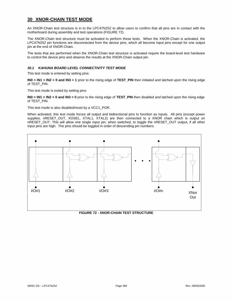
SMSC DS – LPC47N252 Page 289 Rev. 09/06/2000
30 XNOR-CHAIN TEST MODE
An XNOR-Chain test structure is in to the LPC47N252 to allow users to confirm that all pins are in contact with themotherboard during assembly and test operations (FIGURE 72).
The XNOR-Chain test structure must be activated to perform these tests. When the XNOR-Chain is activated, theLPC47N252 pin functions are disconnected from the device pins, which all become input pins except for one outputpin at the end of XNOR-Chain.
The tests that are performed when the XNOR-Chain test structure is activated require the board-level test hardwareto control the device pins and observe the results at the XNOR-Chain output pin.
30.1 KAHUNA BOARD LEVEL CONNECTIVITY TEST MODE
This test mode is entered by setting pins:
IN0 = IN1 = IN2 = 0 and IN3 = 1 prior to the rising edge of TEST_PIN then initiated and latched upon the rising edgeof TEST_PIN.
This test mode is exited by setting pins:
IN0 = IN1 = IN2 = 0 and IN3 = 0 prior to the rising edge of TEST_PIN then disabled and latched upon the rising edgeof TEST_PIN.
This test mode is also disabled/reset by a VCC1_POR.
When activated, this test mode forces all output and bidirectional pins to function as inputs. All pins (except powersupplies, nRESET_OUT, XOSEL, XTAL1, XTAL2) are then connected to a XNOR chain which is output onnRESET_OUT. This will allow one single input pin, when switched, to toggle the nRESET_OUT output, if all otherinput pins are high. The pins should be toggled in order of descending pin numbers.
I/O#1 I/O#2 I/O#3 I/O#n XNorOut
FIGURE 72 - XNOR-CHAIN TEST STRUCTURE

SMSC DS – LPC47N252 Page 290 Rev. 09/06/2000
31 LPC47N252 CONFIGURATION
31.1 OVERVIEW
The Configuration of the LPC47N252 is very flexible and is based on the configuration architecture implemented intypical Plug-and-Play components.
The LPC47N252 is designed for motherboard designs in which the resources required by their components areknown. With its flexible resource allocation architecture, the LPC47N252 allows the BIOS to assign resources atPOST.
31.2 CONFIGURATION REGISTER ACCESS
Only two states are defined (Run and Configuration). In the Run State the chip will always be ready to enter theConfiguration State.
The desired configuration registers are accessed in two steps:
Write the index of the Logical Device Number Configuration Register (i.e., 0x07) to the INDEX PORT and then writethe number of the desired logical device to the DATA PORT.
Write the address of the desired configuration register within the logical device to the INDEX PORT and then write orread the configuration register through the DATA PORT.
Note: If accessing the Global Configuration Registers, step (a) is not required.
31.2.1 PRIMARY CONFIGURATION ADDRESS DECODER
The logical devices are configured through three Configuration Access Ports (CONFIG, INDEX and DATA). TheBIOS uses these ports to initialize the logical devices at POST (Table 310).
The MODE pin is a hardware configuration pin that sets the default Configuration Access Port base address atpower-up. The Configuration Ports base address can also be changed using the configuration ports base addressregister (see Base Address Configuration Registers).
Table 310 - LPC47N252 Configuration Access Ports
PORT NAME
MODE PIN = 0(10K PULL-DOWN RESISTOR
OR TIE TO GND)
MODE PIN = 1(10K PULL-UP RESISTOR
OR TIE TO VCC1) TYPE
CONFIG PORT 0x02E 0x04E Write
INDEX PORT 0x02E 0x04E Read/Write
DATA PORT INDEX PORT + 1 Read/Write
Note 67: This address can be changed by configuration registers 26h and 27h.
31.2.1.1 Entering the Configuration State
The INDEX and DATA ports are effective only when the chip is in the Configuration State. The device enters theConfiguration State when the following Config Key is successfully written to the CONFIG PORT.
Config Key = < 0x55>
31.2.1.2 Exiting the Configuration State
The device exits the Configuration State when the following Config Key is successfully written to the CONFIG PORTaddress.
Config Key = < 0xAA>
31.2.1.3 Read Accessing Configuration Port
The Configuration Port reads back a float condition when not in the Configuration State. The Configuration Portreads back 0x00, after the Configuration Key 0x55 has been written to the Configuration Port, but prior any furtherwrites to the Configuration Port. After the Configuration Index Register has been written to at least once (in theConfiguration State,) then the last value written to the Configuration Index Register (via the Configuration Port) canbe read back.

SMSC DS – LPC47N252 Page 291 Rev. 09/06/2000
31.2.2 CONFIGURATION SEQUENCE EXAMPLE
To program the configuration registers, the following sequence must be followed:
Enter Configuration Mode
Configure the Configuration Registers
Exit Configuration Mode
The following is an example of a configuration program in Intel 8086 assembly language.
; -- -- - -- -- - -- -- - -- -- - -- -- - -- -. ; E NT E R CO N FI GU R AT IO N M OD E | ; -- -- - -- -- - -- -- - -- -- - -- -- - -- -' M OV D X, 02 E HM OV A X, 05 5 HO UT D X, AL ; -- -- - -- -- - -- -- - -- -- - -- -- - -- -. ; C ON F IG UR E R EG I ST ER CR E0 , | ; L OG I CA L DEV IC E 8 | ; -- -- - -- -- - -- -- - -- -- - -- -- - -- -' M OV D X, 02 E HM OV A L, 07 H O UT D X, AL ;P oi n t to LD # Con fi g R eg M OV D X, 02 F HM OV A L, 0 8 HOUT DX,AL;Point to Logical Device 8; M OV D X, 02 E HM OV A L, E0 H O UT D X, AL ; P oi n t to CR E0 M OV D X, 02 f HM OV A L, 02 H O UT D X, AL ; U pd a te C R E0 ; -- -- - -- -- - -- -- - -- -- - -- -- - -- -- . ; E XI T C ON F IG UR A TI ON MO DE |; -- -- - -- -- - -- -- - -- -- - -- -- - -- -- ' M OV D X, 02 E HM OV A X, 0A A HOUT DX,AL.

SMSC DS – LPC47N252 Page 292 Rev. 09/06/2000
31.2.3 BASE ADDRESS CONFIGURATION REGISTERS
The LPC47N252 configuration ports base address is relocatable beyond the two addressing options provided by theMODE pin. The ability to relocate the configuration ports base address can prevent address conflicts. Registers CR26and CR27 enable the relocatable configuration ports base address function. CR26 is the configuration ports baseaddress least significant byte; CR27 is the most significant byte (Table 311). The configuration ports base address isrelocatable on even-byte boundaries; i.e., A0 = “0”. Valid configuration ports base address values are 0x0000 –0x0FFE.
Prior to Vcc2 POR the configuration ports base address are undefined, At Vcc2 POR, the configuration ports baseaddress is determined by the MODE pin.
To relocate the configuration ports base address after power-up, first write the lower address byte (LSB) of the newbase address to CR26 and then write the upper address bits to CR27. Note: Writing CR27 changes the configurationports base address.
Table 311 - Configuration Port Address RegistersDESCRIPTION
INDEX TYPE HARD RESET
(See Note 68)
REGISTER NAME D7 D6 D5 D4 D3 D2 D1 D0
GLOBAL CONFIGURATION REGISTERS
0x262 R/W MODE = 0: 0x2E
MODE = 1: 0x4E
Configuration PortBase Address Byte 0(LSB)
A7 A6 A5 A4 A3 A2 A1 “0”
0x273 R/W MODE = 0: 0x00MODE = 1: 0x00
Configuration PortBase Address Byte 1(MSB)
“0” “0” “0” “0” A11 A10 A9 A8
Note 68: The MODE pin determines the configuration port base address following Hard Reset ConfigurationRegister (See Section 31.2.4.1.) Soft Reset Configuration Register has no effect on CR26 and CR27
Note 69: The configuration ports base address is relocatable on even-byte boundaries; i.e., A0 = “0”.
Note 70: Writing CR27 changes the configuration ports base address.
31.2.4 CONFIGURATION REGISTER RESET CONDITIONS
31.2.4.1 Hard Reset Configuration Register
HARD RESET = VCC2 POR or nRESET_OUT pin asserted.
(See section 11.8.3.5, Output Enable Register on page 134 for description 8051 control of nRESET_OUT)
31.2.4.2 Soft Reset Configuration Register
SOFT RESET = Configuration Control Register Bit0 set to a one by host.
31.3 CONFIGURATION REGISTER MAP
The LPC47N252 Configuration register map is shown below in Table 312.
Table 312 - LPC47N252 Configuration Register Map
INDEX TYPEHARDRESET
SOFTRESET CONFIGURATION REGISTER NAME
0x02 W 0x00 0x00 Config Control
0x03 - - - RESERVED
0x07 R/W 0x00 0x00 Logical Device Number
0x17 - - - RESERVED
0x20 R 0x0E 0x0E LPC 47N 252 Device ID
0x21 R 0x00 0x01 Device Rev – hard wired
0x22 R/W 0x00 n/a Power Control

SMSC DS – LPC47N252 Page 293 Rev. 09/06/2000
INDEX TYPEHARDRESET
SOFTRESET CONFIGURATION REGISTER NAME
0x23 R/W 0x00 n/a Power Mgmt
0x24 R/W 0x04 n/a OSC
0x25 R/W 0x04 n/a DeviceMode
0x26 R/W Configuration Port Base Address (LSB)
0x27 R/WSee Note 68 above.
Configuration Port Base Address (MSB)
0x28 – 0x2F - 0x00 0x00 RESERVED (Test Mode Registers)
LOGICAL DEVICE 0 CONFIGURATION REGISTERS (FDC)
0x30 R/W 0x00 0x00 Activate
0x60,0x61
R/W 0x03,0xF0
0x03,0xF0
Primary Base I/O Address
0x70 R/W 0x06 0x06 Primary Interrupt Select
0x74 R/W 0x02 0x02 DMA channel Select
0xF0 R/W 0x0E n/a FDD Mode Register
0xF1 R/W 0x00 n/a FDD Option Register
0xF2 R/W 0xFF n/a FDD Type Register
0xF4 R/W 0x00 n/a FDD0
0xF5 R/W 0x00 n/a FDD1
LOGICAL DEVICE 1 CONFIGURATION REGISTERS (PM1)
0x30 R/W 0x00 0x00 Activate
0x60,0x61
R/W 0x00,0x00
0x00,0x00
Primary Base I/O Address
LOGICAL DEVICE 2 CONFIGURATION REGISTERS (RESERVED)
LOGICAL DEVICE 3 CONFIGURATION REGISTERS (PARALLEL PORT)
0x30 R/W 0x00 0x00 Activate
0x60,0x61
R/W 0x00,0x00
0x00,0x00
Primary Base I/O Address
0x70 R/W 0x00 0x00 Primary Interrupt Select
0x74 R/W 0x04 0x04 DMA channel Select
0xF0 R/W 0x3C n/a Parallel Port Mode Register
0xF1 R/W 0x00 n/a Parallel Port CnfgB shadow Register
LOGICAL DEVICE 4 CONFIGURATION REGISTERS (SERIAL PORT 1)
0x30 R/W 0x00 0x00 Activate
0x60,0x61
R/W 0x00,0x00
0x00,0x00
UART Register Base I/O Address
0x70 R/W 0x00 0x00 Primary Interrupt Select
0xF0 R/W 0x00 n/a Serial Port 1 Mode Register
LOGICAL DEVICE 5 CONFIGURATION REGISTERS (INFRARED)
0x30 R/W 0x00 0x00 Activate
0x60,
0x61
R/W 0x00,
0x00
0x00,
0x00
Primary Base I/O Address
0x62, 0x63 R/W 0x00, 0x00 0x00, 0x00 SCE Register Base I/O Address
0x70 R/W 0x00 0x00 Primary Interrupt Select
0x74 R/W 0x04 0x04 IRCC 2.0 DMA Channel Select
0xF0 R/W 0x00 n/a Mode Register
0xF1 R/W 0x02 n/a IR Options Register
0xF2 R/W 0x03 n/a IR Half Duplex Timeout
0xF7 R/W 0x00 0x00 Software Select A
0xF8 R/W 0x00 0x00 Software Select B

SMSC DS – LPC47N252 Page 294 Rev. 09/06/2000
INDEX TYPEHARDRESET
SOFTRESET CONFIGURATION REGISTER NAME
LOGICAL DEVICE 6 CONFIGURATION REGISTERS (RTC)
0x30 R/W 0x00 0x00 Activate
0x60,
0x61
R/W 0x00,
0x70
0x00,
0x70
RTC Bank 0 Primary Base Address
0x62, 0x63 R/W 0x00, 0x74 0x00, 0x74 RTC Bank 1 Primary Base Address
0x70 R/W 0x00 0x00 Primary Interrupt Select
0xF0 R/W 0x00 n/a Real Time Clock Mode Register
00xF1 R - - Shadowed RTC/CMOS Bank 0 Index Register
LOGICAL DEVICE 7 CONFIGURATION REGISTERS (KBD)
0x30 R/W 0x00 0x00 Activate
0x70 R/W 0x00 0x00 Primary Interrupt Select
0x72 R/W 0x00 0x00 Second Interrupt Select
0xF0 R/W 0x00 0x00 KRST_GA20
LOGICAL DEVICE 8 CONFIGURATION REGISTERS (EC)
0x30 R/W 0x00 0x00 Activate
0x60, 0x61 R/W 0x00, 0x62 0x00, 0x62 ECI Register Base I/O Address
LOGICAL DEVICE 9 CONFIGURATION REGISTERS (MAILBOX)
0x30 R/W 0x00 0x00 Activate
0x60, 0x61 R/W 0x00, 0x00 0x00, 0x00 Mailbox Register Base I/O Address
LOGICAL DEVICE A CONFIGURATION REGISTERS (LGPIO)
0x30 R/W 0x00 0x00 Activate
0x60, 0x61 R/W 0x00, 0x00 0x00, 0x00 Mailbox Register Base I/O Address
31.4 CHIP LEVEL (GLOBAL) CONTROL/CONFIGURATION REGISTERS[0X00-0X2F]
The chip-level (global) registers lie in the address range [0x00-0x2F]. All unimplemented registers and bits ignorewrites and return zero when read.
The INDEX PORT is used to select a configuration register in the chip. The DATA PORT is then used to access theselected register. These registers are accessible only in the Configuration State.
Table 313 - Global Configuration RegistersREGISTER ADDRESS DESCRIPTION
CHIP (GLOBAL) CONTROL REGISTERS
0x00 –0x01 Reserved, Writes are ignored, reads return 0.
Config Control 0x02 W The hardware automatically clears this bit after the write; there isno need for software to clear the bits.
Bit [0] = 1: Soft Reset; Refer to Table 312 for the soft reset valuefor each register.
Card Level Reserved 0x03W Reserved - Writes are ignored, reads return 0.
0x04 - 0x06 Reserved - Writes are ignored, reads return 0.
Logical Device # 0x07 R/W A write to this register selects the current logical device. Thisallows access to the control and configuration registers for eachlogical device. Note: The Activate command operates only on theselected logical device.
Card Level Reserved 0x08 - 0x1F Reserved - Writes are ignored, reads return 0.
CHIP (GLOBAL ) CONTROL REGISTERS
Device IDHard Wired
0x20 R A read-only register which provides device identification.:Bits[7-0] = 0x0E when read
Device RevHard Wired
0x21 R A read-only register which provides device revision information.
Bits[7-0] = 0x01 when read

SMSC DS – LPC47N252 Page 295 Rev. 09/06/2000
REGISTER ADDRESS DESCRIPTION
PowerControl 0x22 R/W Bit[0] FDC PowerBit[1:2] Reserved (read as 0)
Bit[3] Parallel Port PowerBit[4] Serial Port 1 Power
Bit[5] Serial Port 2 PowerBit[6:7] Reserved (read as 0)
=0 Power off or disabled=1 Power on or Enabled
Power Mgmt 0x23 R/W Bit[0] FDC (see Note in section 10, FDC Power Management)Bit[1:2] Reserved (read as 0)Bit[3] Parallel Port
Bit[4] Serial Port 1Bit[5] Serial Port 2
Bit[6:7] Reserved (read as 0)=0 Power off or disabled=1 Power on or Enabled
OSC 0x24 R/W Bit[1:0] Reserved, set to “0”Bit[3:2] OSC
=01 OSC is on, BRG clock is on when PWRGD is active, OSC isoff and BRG Clock is disabled (default)=10 Same as above (01) case
=00 OSC is on, BRG Clock Enabled=11 OSC is off, BRG Clock is disabled
Bit[6:4] CLK_OUT Select=[0,0,0] CLK_OUT = 1.8432 MHz
=[0,0,1] CLK_OUT = 14.318 MHz=[0,1,0] CLK_OUT = 16 MHz=[0,1,1] CLK_OUT = 24 MHz
=[1,0,0] CLK_OUT = 48 MHz=[1,0,1] Reserved
=[1,1,X] Reserved
Bit[7] nIRQ8 Polarity
=0 nIRQ8 is active high=1 nIRQ8 is active low
Note: This polarity bit not only affects the nIRQ8 pin, but is alsoreflected in the Serial IRQ sample phase for the IRQ8 Frame forthe Serial IRQ Bus.
Device Mode 0x25 R/W Bit [1-0] Reserved – writes ignored, reads return “0”.
Bit[2] SerIRQ Mode (Note 71)= 0 : Serial IRQ Disabled.= 1 : Serial IRQ Enabled
(Default).Bit [4:3] Parallel Port FDC
= [0:0] Normal= [0:1] PPFD1 Mode= [1:0] PPFD2 Mode
= [1:1] ReservedBit [7:5] Reserved – writes ignored, reads return “0”.

SMSC DS – LPC47N252 Page 296 Rev. 09/06/2000
REGISTER ADDRESS DESCRIPTION
Registers Base Address 0x26-0x27 See section 31.2.3, Base Address Configuration Registers onpage 292.
Test Registers 0x28-0x2B SMSC Test Mode Registers, Reserved for SMSC.
TEST 0 0x2C Test Modes - Reserved for SMSC. Users should not write to thisregister, may produce undesired results.
TEST 1 0x2D R/W Test Modes : Reserved for SMSC. Users should not write to thisregister; may produce undesired results.
TEST 2 0x2E R/W Test Modes - Reserved for SMSC. Users should not write to thisregister; may produce undesired results.
TEST 3 0x2F R/W Test Modes - Reserved for SMSC. Users should not write to thisregister; may produce undesired results.
Note 71: The SerIRQ Mode bit controls the SER_IRQ pin, the nCLKRUN pin and the affects of LPC DMA requestson nCLKRUN (see section 28.2.2 nCLKRUN Support for LPC DMA Cycle on page 284).
31.5 LOGICAL DEVICE CONFIGURATION/CONTROL REGISTERS [0X30-0XFF]
Used to access the registers that are assigned to each logical unit. This chip supports ten logical units and has tensets of logical device registers:
Floppy
PM1
Parallel
Serial 1
IRCC 2.
Real Time Clock
Keyboard Controller
Embedded Controller
Mailbox Interface
LPC/8051-addressable GPIO
A separate set (bank) of control and configuration registers exists for each Logical Device and is selected with theLogical Device # Register (0x07). The INDEX PORT is used to select a specific logical device register. Theseregisters are then accessed through the DATA PORT. The Logical Device registers are accessible only when thedevice is in the Configuration State The logical register addresses are listed in Table 314.
Table 314 - Logical Device Configuration RegistersLOGICAL DEVICE
REGISTER ADDRESS DESCRIPTION
Activate (0x30) Bits[7:1] Reserved, set to “0”.
Bit[0]= 1 Activates the logical device currentlyselected through the Logical Device #register.= 0 Logical device currently selected isinactive.
Logical Device Control (0x31-0x37) Reserved - Writes are ignored, reads return“0”.
Logical Device Control (0x38-0x3F) Vendor Defined – Reserved - Writes areignored, reads return “0”.
Memory Base Address (0x40-0x5F) Reserved - Writes are ignored, reads return“0”.
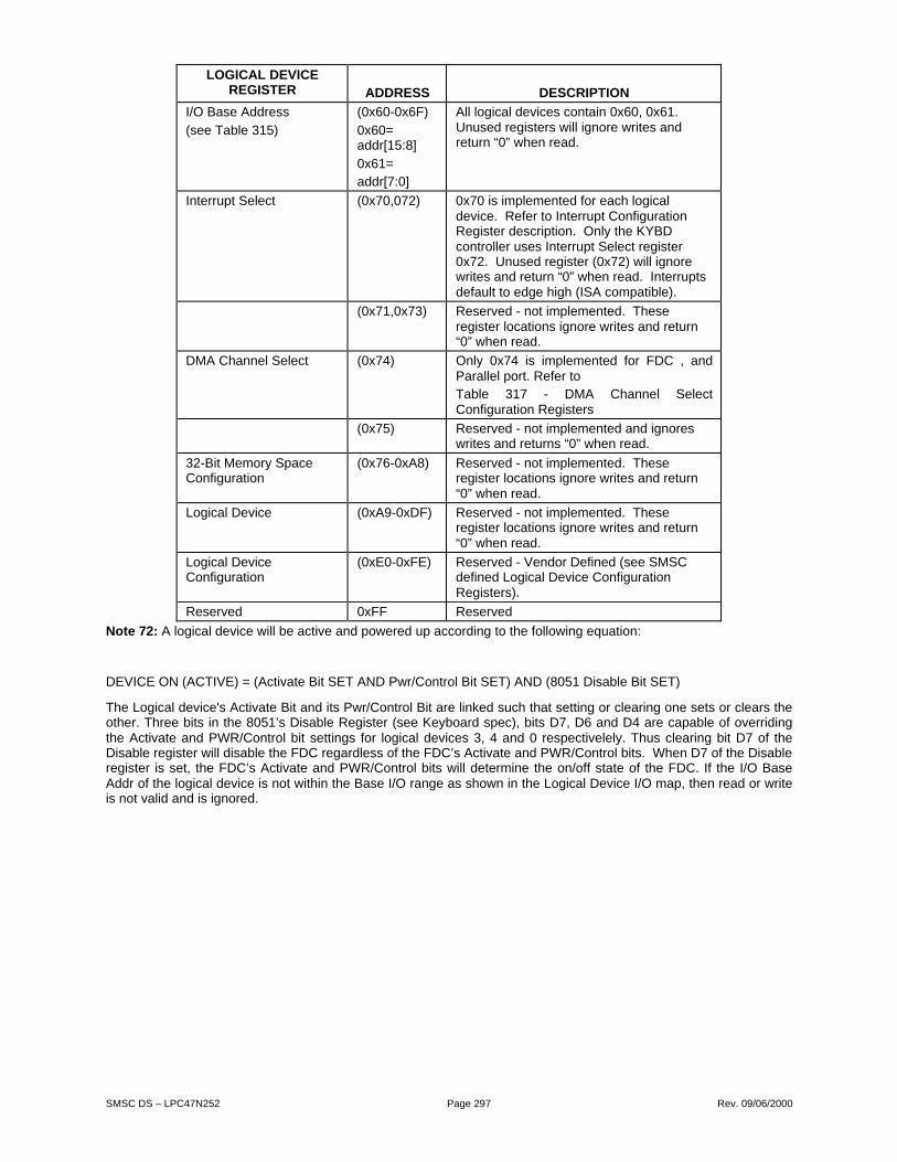
SMSC DS – LPC47N252 Page 297 Rev. 09/06/2000
LOGICAL DEVICEREGISTER ADDRESS DESCRIPTION
I/O Base Address
(see Table 315)
(0x60-0x6F)
0x60=addr[15:8]
0x61=addr[7:0]
All logical devices contain 0x60, 0x61.Unused registers will ignore writes andreturn “0” when read.
Interrupt Select (0x70,072) 0x70 is implemented for each logicaldevice. Refer to Interrupt ConfigurationRegister description. Only the KYBDcontroller uses Interrupt Select register0x72. Unused register (0x72) will ignorewrites and return “0” when read. Interruptsdefault to edge high (ISA compatible).
(0x71,0x73) Reserved - not implemented. Theseregister locations ignore writes and return“0” when read.
DMA Channel Select (0x74) Only 0x74 is implemented for FDC , andParallel port. Refer toTable 317 - DMA Channel SelectConfiguration Registers
(0x75) Reserved - not implemented and ignoreswrites and returns “0” when read.
32-Bit Memory SpaceConfiguration
(0x76-0xA8) Reserved - not implemented. Theseregister locations ignore writes and return“0” when read.
Logical Device (0xA9-0xDF) Reserved - not implemented. Theseregister locations ignore writes and return“0” when read.
Logical DeviceConfiguration
(0xE0-0xFE) Reserved - Vendor Defined (see SMSCdefined Logical Device ConfigurationRegisters).
Reserved 0xFF Reserved
Note 72: A logical device will be active and powered up according to the following equation:
DEVICE ON (ACTIVE) = (Activate Bit SET AND Pwr/Control Bit SET) AND (8051 Disable Bit SET)
The Logical device's Activate Bit and its Pwr/Control Bit are linked such that setting or clearing one sets or clears theother. Three bits in the 8051’s Disable Register (see Keyboard spec), bits D7, D6 and D4 are capable of overridingthe Activate and PWR/Control bit settings for logical devices 3, 4 and 0 respectivelely. Thus clearing bit D7 of theDisable register will disable the FDC regardless of the FDC’s Activate and PWR/Control bits. When D7 of the Disableregister is set, the FDC’s Activate and PWR/Control bits will determine the on/off state of the FDC. If the I/O BaseAddr of the logical device is not within the Base I/O range as shown in the Logical Device I/O map, then read or writeis not valid and is ignored.
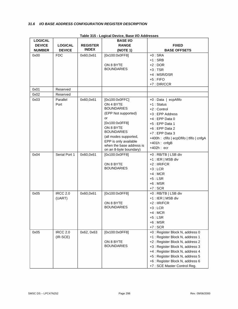
SMSC DS – LPC47N252 Page 298 Rev. 09/06/2000
31.6 I/O BASE ADDRESS CONFIGURATION REGISTER DESCRIPTION
Table 315 - Logical Device, Base I/O AddressesLOGICALDEVICE
NUMBER
LOGICAL
DEVICE
REGISTERINDEX
BASE I/ORANGE
(NOTE 1)
FIXED
BASE OFFSETS
0x00 FDC 0x60,0x61 [0x100:0x0FF8]
ON 8 BYTEBOUNDARIES
+0 : SRA+1 : SRB
+2 : DOR+3 : TSR
+4 : MSR/DSR+5 : FIFO+7 : DIR/CCR
0x01 Reserved
0x02 Reserved
0x03 ParallelPort
0x60,0x61 [0x100:0x0FFC]ON 4 BYTEBOUNDARIES
(EPP Not supported)or
[0x100:0x0FF8]ON 8 BYTEBOUNDARIES
(all modes supported,EPP is only availablewhen the base address ison an 8-byte boundary)
+0 : Data | ecpAfifo+1 : Status+2 : Control
+3 : EPP Address+4 : EPP Data 0
+5 : EPP Data 1+6 : EPP Data 2+7 : EPP Data 3
+400h : cfifo | ecpDfifo | tfifo | cnfgA+401h : cnfgB
+402h : ecr
0x04 Serial Port 1 0x60,0x61 [0x100:0x0FF8]
ON 8 BYTEBOUNDARIES
+0 : RB/TB | LSB div
+1 : IER | MSB div+2 : IIR/FCR+3 : LCR
+4 : MCR+5 : LSR
+6 : MSR+7 : SCR
0x05 IRCC 2.0
(UART)
0x60,0x61 [0x100:0x0FF8]
ON 8 BYTEBOUNDARIES
+0 : RB/TB | LSB div
+1 : IER | MSB div+2 : IIR/FCR
+3 : LCR+4 : MCR+5 : LSR
+6 : MSR+7 : SCR
0x05 IRCC 2.0(IR-SCE)
0x62, 0x63 [0x100:0x0FF8]
ON 8 BYTEBOUNDARIES
+0 : Register Block N, address 0+1 : Register Block N, address 1+2 : Register Block N, address 2
+3 : Register Block N, address 3+4 : Register Block N, address 4
+5 : Register Block N, address 5+6 : Register Block N, address 6+7 : SCE Master Control Reg.

SMSC DS – LPC47N252 Page 299 Rev. 09/06/2000
LOGICALDEVICE
NUMBERLOGICALDEVICE
REGISTERINDEX
BASE I/ORANGE
(NOTE 1)FIXED
BASE OFFSETS
0x06 RTC 0x60, 0x61
0x62, 0x63
[0x100:0x0FFE]
[0x100:0x0FFD]
Bank 0 Base address+0 : Address Register
+1 : Data RegisterBank 1 Base address+0 : Address Register
+2 : Data Register
0x07 KYBD N/a Not Relocatable
Fixed Base Address
0x60 : Data Register
0x64 : Command/Status Reg.
0x08 ECI 0x60, 0x612 [0x0000:0xFFA]Relocatable
+0 : Data Register3
+4 : Command Register
0x09 MailboxRegister
0x60, 0x61 [0x0000:0x0FFE] +0 : Index+1 : Data
0x0A LPC/8051GPIO
0x60, 0x61 [0x100:0x0FF0]
ON 16 BYTEBOUNDARIES
+0 : LGPIO DIR G+1 : LGPIO INPUT G+2 : LGPIO OUTPUT G
+3 : LGPIO DIR H+4 : LGPIO INPUT H
+5 : LGPIO OUTPUT H+6 : LGPIO DIR I+7 : LGPIO INPUT I
+8 : LGPIO OUTPUT I
Note 1: This chip uses all LPC address bits to decode the base address of each of its logical devices.
Note 2: Please refer to Table 61 – ECI Configuration Registers (LDN8) for further description.
Note 3: Please refer to Table 62 – ECI Run-Time Registers for further description.
31.7 INTERRUPT SELECT CONFIGURATION REGISTER DESCRIPTION
Table 316 - Interrupt Select Configuration RegistersNAME REG INDEX DEFINITION
Interruptrequest level
select 0
0x70 (R/W) Bit [3-0] Select which interrupt level is used forInterrupt 0.
0x00=no interrupt selected.0x01=IRQ1
0x02=IRQ2
• • •0x0E= IRQ140x0F= IRQ15All pin-type interrupts are edge high (exceptECP/EPP). Each Logical Device’s interrupts selectedthrough this register physically select the interrupts tobe used by the LPC47N252 for either the Serial IRQinterface or for the individual pin-type ISA interrupts ifselected. Setting the IRQ through this register for theParallel Port is not reflected in the Enhanced Parallelport cnfgB register, software must set the DMA/IRQbits in the Parallel Port logical device config register0xF1 (Parallel Port CnfgB shadow register).

SMSC DS – LPC47N252 Page 300 Rev. 09/06/2000
Note: An interrupt is activated by setting the Interrupt Request Level Select 0 register to a non-zero value AND:
1) for the FDC logical device by setting DMAEN, bit D3 of the Digital Output Register.2) for the PP logical device by setting IRQE, bit D4 of the Control Port and in addition3) for the PP logical device in ECP mode by clearing serviceIntr, bit D2 of the ecr.4) for the Serial Port logical device by setting any combination of bits D0-D3 in the IER and by setting the OUT2 bit
in the UART's Modem Control (MCR) Register.5) for the RTC by (refer to the RTC section of this specification).6) for the KYBD by (refer to the KYBD controller section of this specification).
31.8 DMA CHANNEL SELECT CONFIGURATION REGISTER DESCRIPTION
Table 317 - DMA Channel Select Configuration RegistersNAME REG INDEX DEFINITION
DMA Channelselect 0
0x74 (R/W) Bit [2:0] Select the DMA Channel.0x00=DMA0
0x01=DMA10x02=DMA20x03=DMA3
0x04-0x07= No DMA active
Note: A DMA channel is activated by setting the DMA Channel Select 0 register to [0x00-0x03]
AND :
for the FDC logical device by setting DMAEN, bit D3 of the Digital Output Register
for the PP logical device in ECP mode by setting dmaEn, bit D3 of the ecr
for the UART2 logical device, by setting the DMA Enable bit. Refer to the IRCC 2.0 specification available fromSMSC
31.9 INTERRUPT AND DMA ENABLE AND DISABLE
Any time the interrupt or DMA for a logical block is disabled by a register bit in that logical block, the interrupt outputand/or DMA request cycles must be disabled. This is in addition to the interrupt and DMA disabled by theConfiguration Registers (activate bit cleared or address outside of valid range or the Interrupt Select register set to0x00 or the DMA Channel Select register set to 0x04).
31.9.1 LOGICAL DEVICE 0 (FDC)
For the following cases, the interrupt and DMA channel used by the FDC are disabled.
Digital Output Register (Base+2) bit D3 (DMAEN) set to "0".
The FDC is in power down (disabled).
31.9.2 LOGICAL DEVICE 5 (SERIAL PORT1)
Modem Control Register (MCR) Bit D2 (OUT2) –
When OUT2 is a logic "0", the serial port interrupt is disabled. Disabling DMA Enable bit, disables DMA for UART2.Refer to the IrCC specification.
31.9.3 LOGICAL DEVICE 5 (SERIAL PORT2/USART)
Interrupt is disabled when:
Modem Control Register (MCR) bit 2 (OUT2) - When OUT2 is a logic “0”, then Logical Device 5’s interrupt is forced toa high impedance state, i.e., disabled. This applies to all UART/IR modes of operation.
DRQ is disabled when:
SCE Configuration Register B bit-0 (DMA Enable) - When the DMA Enable bit is a logic “0”, then logical device 5’sD MA channel i s disabled. When the DMA Enable bit is set to logic “1”, then logical device 5’s D MA channel i sactivated.

SMSC DS – LPC47N252 Page 301 Rev. 09/06/2000
31.9.4 PARALLEL PORT
SPP and EPP modes: Control Port (Base+2) bit D4 (IRQE) set to "0", IRQ is disabled (high impedance).
ECP Mode:
(DMA) dmaEn from ecr register.
IRQ - See table below.
MODE (FROM ECR REGISTER) IRQ CONTROLLED BY DNA CONTROLLED BY000 PRINTER IRQE dmaEn
001 SPP IRQE dmaEn
010 FIFO (on) dmaEn
011 ECP (on) dmaEn
100 EPP IRQE dmaEn
101 RES IRQE dmaEn
110 TEST (on) dmaEn
111 CONFIG IRQE dmaEn
31.9.5 REAL TIME CLOCK (RTC)
See to section 27, REAL TIME CLOCK on page 275.
31.9.6 KEYBOARD CONTROLLER (KYBD)
See KEYBOARD CONTROLLER SECTION.
31.10 SMSC DEFINED LOGICAL DEVICE CONFIGURATION REGISTERS
The SMSC Specific Logical Device Configuration Registers reset to their default values only on hard resets. Theseregisters are not effected by soft resets. See section 31.2.4, Configuration Register Reset Conditions on page 292.
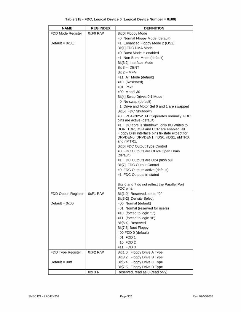
SMSC DS – LPC47N252 Page 302 Rev. 09/06/2000
Table 318 - FDC, Logical Device 0 [Logical Device Number = 0x00]
NAME REG INDEX DEFINITION
FDD Mode Register
Default = 0x0E
0xF0 R/W Bit[0] Floppy Mode
=0 Normal Floppy Mode (default)=1 Enhanced Floppy Mode 2 (OS2)Bit[1] FDC DMA Mode
=0 Burst Mode is enabled=1 Non-Burst Mode (default)
Bit[3:2] Interface ModeBit 3 – IDENTBit 2 – MFM
=11 AT Mode (default)=10 (Reserved)
=01 PS/2=00 Model 30Bit[4] Swap Drives 0,1 Mode
=0 No swap (default)=1 Drive and Motor Sel 0 and 1 are swappedBit[5] FDC Shutdown
=0 LPC47N252 FDC operates normally, FDCpins are active (default)
=1 FDC core is shutdown, only I/O Writes toDOR, TDR, DSR and CCR are enabled, allFloppy Disk interface pins tri-state except forDRVDEN0, DRVDEN1, nDS0, nDS1, nMTR0,and nMTR1.
Bit[6] FDC Output Type Control=0 FDC Outputs are OD24 Open Drain(default)
=1 FDC Outputs are O24 push pullBit[7] FDC Output Control
=0 FDC Outputs active (default)=1 FDC Outputs tri-stated
Bits 6 and 7 do not reflect the Parallel PortFDC pins.
FDD Option Register
Default = 0x00
0xF1 R/W Bit[1:0] Reserved, set to “0”Bit[3-2] Density Select=00 Normal (default)
=01 Normal (reserved for users)=10 (forced to logic “1”)
=11 (forced to logic “0”)Bit[5:4] ReservedBit[7:6] Boot Floppy
=00 FDD 0 (default)=01 FDD 1
=10 FDD 2=11 FDD 3
FDD Type Register
Default = 0Xff
0xF2 R/W Bit[1:0] Floppy Drive A Type
Bit[3:2] Floppy Drive B TypeBit[5:4] Floppy Drive C Type
Bit[7:6] Floppy Drive D Type
0xF3 R Reserved, read as 0 (read only)

SMSC DS – LPC47N252 Page 303 Rev. 09/06/2000
NAME REG INDEX DEFINITION
FDD0
Default = 0x00
0xF4 R/W Bit[1:0] Drive Type Select (DT1, DT0) (See Table 32 on page 15).
Bit[2] Read as “0” (read only)Bit[3:4] Data Rate Table Select (DRT1,DRT0)
Bit[5] Read as “0” (read only)Bit[6] Precomp Disable
= 0 Use Precompensation
= 1 No PrecompensationBit[7] Read as “0” (read only)
FDD1 0xF5 R/W Refer to definition and default for 0xF4
Table 319 - Parallel Port, Logical Device 3 [Logical Device Number = 0x03]
NAMEREG
INDEX DEFINITIONPP Mode Register
Default = 0x3C
0xF0 R/W Bit [2:0] Parallel Port Mode= 100 Printer Mode (default)= 000 Standard and Bi-directional (SPP) Mode= 001 EPP-1.9 and SPP Mode= 101 EPP-1.7 and SPP Mode= 010 ECP Mode= 011 ECP and EPP-1.9 Mode= 111 ECP and EPP-1.7 Mode
Bit[6:3] ECP FIFO Threshold0111b (default)
Bit[7] PP Interrupt TypeNot valid when the parallel port is in the Printer Mode (100) or theStandard $ Bi-Directional Mode (000)
=1 Pulsed Low, released to high-Z (665/666)=0 IRW follows nACK when parallel port in EPP Mode or [Printer,SPP, EPP] under ECP, TEST or Centronics FIFO Mode.
Parallel PortCnfgB shadowRegister
Default = 0x00
0xF1 R/W Bits [2:0] Parallel Port DMA channel Select= 000 h/w jumpered 8-bit DMA (default)= 001 DMA channel 1= 010 DMA channel 2= 011 DMA channel 3
Bits [5:3] Parallel Port IRQ line Select= 000 h/w jumpered IRQ (default)= 001 IRQ 7= 010 IRQ 9= 011 IRQ 10= 100 IRQ 11= 101 IRQ 14= 110 IRQ 15= 111 IRQ 5
Bit [6] Reserved, ignores writes, returns “0” on reads.
Bit [7] Timeout_Select (NOTES: the Timeout_Select bit affects theEPP Status Register Timeout bit. The Timeout_Select bit does notappear in the Parallel Port CnfgB register).= 0 Timeout bit cleared on trailing edge of EPP Status RegisterRead (default).= 1 Timeout bit cleared on a write of ‘1’ to the Timeout bit.
NOTE: The DMA/IRQ bits in this register are reflected in theEnhanced Parallel Port’s read-only cnfgB register.

SMSC DS – LPC47N252 Page 304 Rev. 09/06/2000
Table 320 - Serial Port 1, LOGICAL DEVICE 4 [LOGICAL DEVICE Number = 0X04]
NAMEREG
INDEX DEFINITION
Serial Port 1Mode Register
Default = 0x00
0xF0 R/W Bit[0] MIDI Mode= 0 MIDI support disabled (default)= 1 MIDI support enabled
Bit[1] High Speed= 0 High Speed Disabled (default)
= 1 High Speed Enabled
Bit[6:2] Reserved, set to “0”
Bit[7] Reserved
Table 321 - Infrared, Logical Device 5 [Logical Device Number = 0x05]
NAMEREG
INDEX DEFINITION
Infrared
Mode Register
Default = 0x00
oxF0 R/W Bit[0] MIDI Mode
=0 MIDI support disabled (default)=1 MIDI support enabled
Bit[1] High Speed=0 High Speed Disabled (default)=1 High Speed Enabled
Bit[7:2] Reserved
IR Option Register
Default = 0x00
oxF1 R/W Bit[0] Receive Polarity=0 Active High=1 Active Low (default)
Bit[1] Transmit Polarity
=0 Active High (Default)=1 Active Low
Bit[2] Duplex Select=0 Full Duplex (Default)
=1 Half Duplex
Bit[5:3] UART/IR Mode
=000 Standard COMM (default)=001 IrDA SIR-A
=010 ASK-IR=011 (IrDA SIR-B)=100 (IrDA HDLC)
=101 (IrDA 4PPM)=110 (Consumer)
=111 (Raw IR)
Bit[7:6] IRCC 2.0 Output Mux
=00 Active Device to COM-RX/COM-TX port (default)=01 Active Device to IRRX/IRTX port
=10 Reserved-use AUX port not mapped to pins thus bothIR and COM ports are inactive=11 Reserved, all ports are inactive

SMSC DS – LPC47N252 Page 305 Rev. 09/06/2000
NAMEREG
INDEX DEFINITION
IR Half Duplex Timeout
Default = 0x03
0xF2 R/W Bit[7:0]
These bits set the half duplex time-out for the IR port. Thisvalue is 0 to 10ms in 100µs increments
=0x00 blank RX/TX during Transmit/Receive
=0x01 blank TX/TX during Xmit/Rcv + 100µs
......
=0x64 blank RX/TX during Xmit/Rcv +10ms
=0x65 - 0xFF: Reserved
See Section 8.4.1, Software Select Registers A and B on page
Table 322 - RTC, LOGICAL DEVICE 6 [LOGICAL DEVICE NUMBER = 0X06]
NAMEREG
INDEX DEFINITION STATE
RTC Mode Register
Default = 0x00
0xF0 R/W Bit[0] = 1 : Lock CMOS RAM 80-9FhBit[1] = 1 : Lock CMOS RAM A0-BFhBit[2] = 1 : Lock CMOS RAM C0-DFh
Bit[3] = 1 : Lock CMOS RAM E0-FEhBit[7:4] Reserved, set to “0”Once set, bit[3:0] can not be cleared by a write; bits[3:0]are cleared on VCC2 Power On Reset, VCC2 Power Off,or upon a Hard Reset (nRESET_OUT asserted). Oncelock bits are set, both the Host and the 8051 are lockedout of accessing the locked locations as long as VCC1and VCC2 are active. When VCC2 goes to 0V, the lockbits are cleared and the 8051 can access this RAM whilenRESET_OUT is asserted.
C
Table 323 - KYBD, LOGICAL DEVICE 7 [LOGICAL DEVICE NUMBER = 0X07]
NAMEREG
INDEX DEFINITION STATE
KRST_GA20 0xf0 R/W
Bit[0] : ENAB_P92= 0 : Port 92 Disabled= 1 : Port 92 Enabled
Bit[7:0] : Reserved, set to “0”.
Note: See 16.5.4 for descriptions of these registers.

SMSC DS – LPC47N252 Page 306 Rev. 09/06/2000
32 ELECTRICAL SPECIFICATIONS
32.1 MAXIMUM GUARANTEED RATINGS*
Operating T em per atur e R ange..................................................................................................................................0oC to +70oC Storage Tem peratur e R ange................................................................................................................................... - 55o to +150oC Lead T em per atur e R ange (solder i ng, 10 seconds) ..........................................................................................................+325oC Positi ve Voltage on any pi n, w i th r espect to Ground ..........................................................................................................+5.5VN egati ve Voltage on any pi n, w i th r espect to Ground......................................................................................................... - 0.3VSuppl y Vol tage Range VCC1 and VCC2 ................................................................................................................VCC1 and VCC2
*Stresses above those listed above could cause permanent damage to the device. This is a stress rating only andfunctional operation of the device at any other condition above those indicated in the operation sections of thisspecification is not implied.
Note: When powering this device from laboratory or system power supplies, it is important that the AbsoluteMaximum Ratings not be exceeded or device failure can result. Some power supplies exhibit voltage spikes on theiroutputs when the AC power is switched on or off. In addition, voltage transients on the AC power line may appear onthe DC output. If this possibility exists, it is suggested that a clamp circuit be used.
Table 324 - Operating ConditionsSYMBOL PARAMETER MIN TYP MAX UNITS
Vcc0 Vbat for RTC 2.4 3.0 3.3 V
Vcc1 Vcc for 8051 3.15 3.3 3.45 V
Vcc2 System Vcc 3.15 3.3 3.45 V
PCI_CLK PCI Clock 33 MHz
XTAL1/XTAL2 RTC Crystal 32.768 kHz
CLOCKI 14.318 Clock Input 14.318 MHz
TA OperatingTemperature
0 70 °C
32.2 DC SPECIFICATIONS
D C EL ECT RIC AL C H AR AC T ER IST IC S (T A = 0°C - 70°C , VCC1 and VCC2= 3.3 VD C) PAR AM ETER SYM BOL M IN T YP M AX U NITS C OM MEN TS
I T yp e Inp u t Bu f fer
Low Input Level
H igh Input Level
VI LI
VI HI 2.0
0.8 V
V
T TL Levels
IS Typ e In p ut B u ff er
Low Input Level
H igh Input Level
Schmi tt Tr i gger Hysteresi s
VI LI S
VI HI S
VHYS
2.2
250
0.8 V
V
m V
Schmi tt Tr i gger
Schmi tt Tr i gger

SMSC DS – LPC47N252 Page 307 Rev. 09/06/2000
PAR AM ETER SYM BOL M IN T YP M AX U NITS C OM MEN TS
ISP T ype In pu t B uf ferwit h 90 A weak p ull-u p
Low Input Level
H igh Input Level
Schmi tt Tr i gger Hysteresi s
VI LI S
VI HI S
VHYS
2.2
250
0.8 V
V
m V
Schmi tt Tr i gger
Schmi tt Tr i gger
ICLK In pu t B uf f er
Low Input Level
H igh Input Level
VI LCK
VI HCK 3.0
0.4 V
V
OCLK2 Cryst al Oscillato rOut pu t
ICLK2 C rystal Oscil lator Input
U se a 32 Khz par al lel r esonant cr ystal osci ll ator. T he load capacitor s are seen bythe cr ystal as two capaci tor s i n ser ies and should be appr oxi matel y 2 tim es the C o ofthe actual cr ystal used ( C 1=2C o). F or exam pl e, a 7.5pF cr ystal should use two 15pF
capaci tors for proper l oading.
Input Leakage
( Al l I and IS buffer s exceptPWR GD &VCC 1_PWR GD )
Low Input Leakage
H igh Input Leakage
II L
II H
- 10
- 10
+10
+10
µ A
µ A
VI N = 0
VI N = VCC or VI N = 5 V.
Input Curr entPWR GD IO H 75 150 µ A VI N = 0
O4 Typ e Bu f fer
Low Output Level
H igh Output Level
Output Leakage
VO L
VO H
IO L
2.4
- 10
0.4
+10
V
V
µ A
IO L = 4 m A
IO H = -2 mA
VI N = 0 to VCC
OD4 T ype B u ff er
Low Output Level
Output Leakage
VO L
IO H - 10
0.4
+10
V
µ A
VO L = 4 m A
IO H = 0 to VCC
O8 Typ e Bu f fer
Low Output Level
H igh Output Level
Output Leakage
VO L
VO H
IO L
2.4
- 10
0.4
+10
V
V
µ A
IO L = 8 m A
IO H = -4 mA
VI N = 0 to VCC
OD8 T ype B u ff er
Low Output Level
Output Leakage
VO L
IO H - 10
0.4
+10
V
µ A
VO L = 8 m A
IO H = 0 to VCC

SMSC DS – LPC47N252 Page 308 Rev. 09/06/2000
PAR AM ETER SYM BOL M IN T YP M AX U NITS C OM MEN TS
O24 T ype B u ff er
Low Output Level
H igh Output Level
Output Leakage
VO L
VO H
IO L
2.4
- 10
0.4
+10
V
V
µ A
IO L = 24 mA
IO H = -12 m A
VI N = 0 to VCC
OD24 T yp e B uf fer
Low Output Level
H igh Output Level
Output Leakage
VO L
VO H
IO L
2.4
- 10
0.4
+10
V
V
µ A
IO L = 24 mA
IO H = -50 m A
VI N = 0 to Vcc
IO12 Type Buffer
Low Output Level
High Output Level
Output Leakage
VOL
VOH
IOL
2.4
-10
0.4
+10
V
V
µA
IOL = 12mA
IOH = -6mA
VIN = 0 to VCC
IO8 Type Buffer
Low Output Level
High Output Level
Output Leakage
Input Leakage
( Al l I and IS buffer s exceptFAD[7:0]
VOL
VOH
IOL
2.4
-10
0.4
+10
V
V
µA
IOL = 8mA
IOH = -4mA
VIN = 0 to VCC
(Note 2)
FAD[7:0]
Input Leakage
Low Input Leakage
H igh Input Leakage
II L
II H
- 100
- 100
+100
+100
nA
nA
VI N = 0
VI N = VCC or VI N = 5 V.
IOD 8 T yp e B uf ferLow Output Level
H igh Input Level
H igh Inputt Level
Output Leakage
VOL
VIH
VIL
0.5
2.0
0.8
V
V
V
IOL=8 mA

SMSC DS – LPC47N252 Page 309 Rev. 09/06/2000
PAR AM ETER SYM BOL M IN T YP M AX U NITS C OM MEN TS
IOD 16 Type Bu ff erLow Output Level
H igh Input Level
H igh Inputt Level
Output Leakage
VOL
VIH
VIL
0.5
2.0
0.8
V
V
V
IOL=16 mA
IOP14 Type Buffer
Low Output Level
High Output Level
Output Leakage
VOL
VOH
IOL
2.4
-10
0.4
+10
V
V
µA
IOL = 14mA
IOH = -14mA
VIN = 0 to 5V
IP Typ e Bu f fer
Low Input Level
H igh Input Level
VI LI
VI HI 2.0
0.8 V
V
IPD T ype B u ff er
Low Input Level
H igh Input Level
VI LI
VI HI
V
V
O12 Type Buffer
Low Output Level
High Output Level
VOL
VOH 2.4
0.4 V
V
IOL = 12mA
IOH = -6mA
OD12 Type Buffer
Low Output Level
Output Leakage
VOL
IOL -10
0.4
+10
V
µA
IOL = 12mA
VIN = 0 to 5V
OD14 Type Buffer
Low Output Level
Output Leakage
VOL
IOL -10
0.4
+10
V
µA
IOL = 14mA
VIN = 0 to 5V
OD16 T yp e B uf fer
Low Output Level
Output Leakage
VOL
IOL -10
0.4
+10
V
µA
IOL = 16mA
VIN = 0 to 5V

SMSC DS – LPC47N252 Page 310 Rev. 09/06/2000
PAR AM ETER SYM BOL M IN T YP M AX U NITS C OM MEN TS
OP14 Type Buffer
Low Output Level
High Output Level
Output Leakage
VOL
VOH
IOL
2.4
-10
0.4
+10
V
V
µA
IOL = 14mA
IOH = -14mA
VIN = 0 to 5V
Note: All output leakage’s ar em easur ed w i th the cur rent pi ns inhigh i mpedance
PCI_C L K Typ e Bu f fer See Specification for PCI SystemsVersion 6.0
PCI_IO T yp e B uf f er See
Specification for PCI SystemsVersion 6.0
PCI_OD T yp e B uf f er See
Specification for PCI SystemsVersion 6.0
ICL K T yp e B uf fer
Low Input Level
H igh Input Level
VI LI
VI HCLK 2.4
0.4 V
V
ICL K2 Type Bu ff er
OCL K2 Type Bu ff er
Use a 32 kHz parallel resonant crystal oscillator. The load capacitors are seen bythe crystal as tow capacitors in series and should be approximately 2 times the C0
of the actual crystal used (c1- co.) For example a 7.5 pF crystal should use two 15pF capacitors for proper loading.
Table 325 - Power Comsumption In Various StatesSupply Current (AMPS) COMMENTSVCC2
(VDC)VCC1
(VDC)8051
STATECLOCKSTATE MIN TYP MAX
3.3 3.3 Run 24 Mhz ICC2
ICC1
15 ma24 ma
20 ma30 ma
FLOPPY @ 1 Meg Data RateACCESS.Bus @ 24 Mhz
3.3 3.3 Run 12 Mhz ICC2
ICC1
13 ma12 ma
15 ma18 ma
FLOPPY @ 500K Data RateACCESS.Bus @ 12 Mhz
3.3 3.3 Run RingOSC
ICC2
ICC1
>1ma8 ma
2 ma10 ma
PLL OnACCESS.Bus Off
3.3 3.3 Idle RingOSC
ICC2
ICC1
>1ma5ma
2 ma7 ma
PLL Off
3.3 3.3 Idle 32 Mhz ICC2
ICC1
tbd tbd Flash program cycle
0 3.3 Run RingOSC
ICC2
ICC1 8 ma 10maPLL OffACCESS.Bus Off
0 3.3 Idle RingOSC
ICC2
ICC1 6 ma 8maPLL OffACCESS.Bus Off
0 3.3 Sleep Stop ICC1 160 µa XOSEL=10 3.3 Sleep Stop ICC1 50 µa 80 µa XOSEL=00 0 ICC0 40µa 60 µa 2.4 < Vcc0 < 4 VDC,
XOSEL=1,0 0 ICC0 0.4µa 1.5 µa 2.4 < Vcc0 < 4 VDC, XOSEL =
0 Note: When a single-ended 32.768kHz clock source is selected (see Section 32kHz Clock Input. The LPC47N252uses the XOSEL pin to select either a 32.768kHz input clock or a 32.768kHz crystal to drive the Real Time ClockInterface (Table 2 - PIN FUNCTION DESCRIPTION). When XOSEL = ‘0’, The RTC uses a 32.768kHz crystalconnected between the XTAL1 and XTAL2 pins. When XOSEL = ‘1’, the RTC is driven by a 32.768kHz single-endedclock source connected to the XTAL2 pin. Start up delay for 32Khz can be 5 seconds.

SMSC DS – LPC47N252 Page 311 Rev. 09/06/2000
32.3 AC SPECIFICATIONS
AC Test ConditionsC APAC ITANC E T A = 25°C; fc = 1M Hz; Vcc = 3.3 VDC
L IM IT S
PAR AM ETER SYM BOL M IN T YP M AX U NIT T EST C ON DIT ION
C lock Input C apaci tance C I N 20 pF
Input Capacitance C I N 10 pF
Output C apaci tance C O UT 20 pF
All pi ns except pi n under test tied to AC gr ound

SMSC DS – LPC47N252 Page 312 Rev. 09/06/2000
33 TIMING DIAGRAMS
33.1 CLOCK AND RESET TIMING
FIGURE 73 - INPUT CLOCK TIMING
Table 326 - Input Clock Timing ParametersNAME DESCRIPTION MIN TYP MAX UNITS
t1 Clock Cycle Time for 14.318 MHz (Note) 69.84 ns
t2 Clock High Time/Low Time for 14.318 MHz 15 ns
tr, tf Clock Rise Time/Fall Time (not shown) 5 ns
Note: Tolerance is ± 0.01%.
t1t3 t2PCI_CLK t5
t44
FIGURE 74 – PCI CLOCK TIMING
NAME DESCRIPTION MIN TYP MAX UNITS
t1 PERIOD 30 33.3 nsec
t2 High Time 12 nsec
t3 Low Time 12 nsec
t4 Rise Time 3 nsec
t5 Fall Time 3 nsec
t1LRESET#
FIGURE 75 - RESET TIMING
NAME DESCRIPTION MIN TYP MAX UNITS
t1 LRESET# width 1 ms
t2
t1
t2
CLOCKI
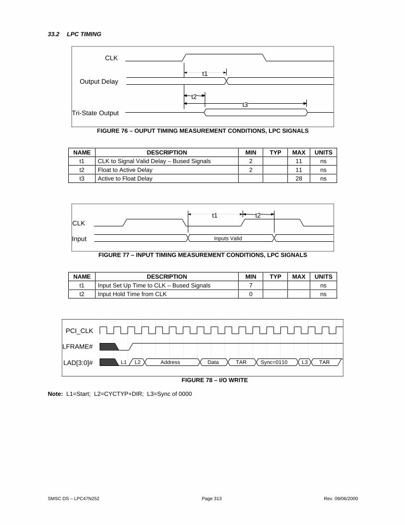
SMSC DS – LPC47N252 Page 313 Rev. 09/06/2000
33.2 LPC TIMING
t3t2
t1
CLK
Output Delay
Tri-State Output
FIGURE 76 – OUPUT TIMING MEASUREMENT CONDITIONS, LPC SIGNALS
N AM E D ESCR IPT ION M IN T YP M AX U NITS
t1 CLK to Signal Valid Delay – Bused Signals 2 11 ns
t2 Float to Active Delay 2 11 ns
t3 Active to Float Delay 28 ns
Inputs Valid
t2t1CLK
Input
FIGURE 77 – INPUT TIMING MEASUREMENT CONDITIONS, LPC SIGNALS
N AM E D ESCR IPT ION M IN T YP M AX U NITS
t1 Input Set Up Time to CLK – Bused Signals 7 ns
t2 Input Hold Time from CLK 0 ns
L1 L2 Address Data TAR Sync=0110 L3 TAR
PCI_CLK
LFRAME#
LAD[3:0]#
FIGURE 78 – I/O WRITE
Note: L1=Start; L2=CYCTYP+DIR; L3=Sync of 0000

SMSC DS – LPC47N252 Page 314 Rev. 09/06/2000
L1 L2 Address TAR Sync=0110 L3 Data TAR
PCI_CLK
LFRAME#
LAD[3:0]#
FIGURE 79 – I/O READ
Note: L1=Start; L2=CYCTYP+DIR; L3=Sync of 0000
Start MSB LSB ACT
PCI_CLK
LDRQ#
FIGURE 80 – DMA REQUEST ASSERTION THROUGH LDRQ#
Start C+D CHL Size TAR Sync=0101 L1 Data TAR
PCI_CLK
LFRAME#
LAD[3:0]#
FIGURE 81 – DMA WRITE (FIRST BYTE)
Note: L1=Sync of 0000
Start C+D CHL Size Data TAR Sync=0101 L1 TAR
PCI_CLK
LFRAME#
LAD[3:0]#
FIGURE 82 – DMA READ (FIRST BYTE)
Note: L1=Sync of 0000

SMSC DS – LPC47N252 Page 315 Rev. 09/06/2000
33.3 FLOPPY DISK TIMING
t3
t1 t2
t4
t5
t6
t7
t8
nDIR
nSTEP
nDS0-1
nINDEX
nRDATA
nWDATA
t9
FIGURE 83 – FLOPPY DISK DRIVE TIMING (AT MODE ONLY)
N AM E D ESCR IPT ION M IN T YP M AX U NITS
t1 nDIR Set Up to STEP Low 4 X*
t2 nSTEP Active Time Low 24 X*
t3 nDIR Hold Time after nSTEP 96 X*
t4 nSTEP Cycle Time 132 X*
t5 nDS0-1 Hold Time from nSTEP Low (Note) 20 X*
t6 nINDEX Pulse Width 2 X*
t7 nRDATA Active Time Low 40 ns
t8 nWDATA Write Data Width Low .5 Y*
t9 nDS0-1, Setup Time nDIR Low (Note) 0 ns*X specifies one MCLK period and Y specifies one WCLK period.MCLK = 16 x Data Rate (at 500 kb/s MCLK = 8 MHz)WCLK = 2 x Data Rate (at 500 kb/s WCLK = 1 MHz)Note: The nDS0-1 setup and hold times must be met by software.

SMSC DS – LPC47N252 Page 316 Rev. 09/06/2000
33.4 EPP TIMING
t9t8
t7t6
t4t5
t3
t2t1nWRITE
PD<7:0>
nDATASTB
nADDRSTB
nWAIT
FIGURE 84 – EPP 1.9 DATA OR ADDRESS WRITE CYCLE
N AM E D ESCR IPT ION M IN T YP M AX U NITS
t1 nWAIT Asserted to nWRITE Asserted (Note 1) 60 185 ns
t2 nWAIT Asserted to nWRITE Change (Note 1) 60 185 ns
t3 nWAIT Asserted to PDATA Invalid (Note 1) 0 ns
t4 PDATA Valid to Command Asserted 10 ns
t5 nWRITE to Command Asserted 5 35 ns
t6 nWAIT Asserted to Command Asserted (Note 1) 60 210 ns
t7 nWAIT Deasserted to Command Deasserted(Note 1)
60 190 ns
t8 Command Asserted to nWAIT Deasserted 0 10 µs
t9 Command Deasserted to nWAIT Asserted 0 ns
Note 1: nWAIT must be filtered to compensate for ringing on the parallel bus cable. WAIT is considered tohave settled after it does not transition for a minimum of 50 nsec.

SMSC DS – LPC47N252 Page 317 Rev. 09/06/2000
t12t11
t10t9
t7t8
t6t5t4t3
t2t1nWRITE
PD<7:0>
nDATASTB
nADDRSTB
nWAIT
FIGURE 85 – EPP 1.9 DATA OR ADDRESS READ CYCLE
N AM E D ESCR IPT ION M IN T YP M AX U NITS
t1 nWAIT Asser ted to nW R IT E D easserted 0 185 ns
t2 nWAIT Asser ted to nW R IT E M odifi ed ( N otes 1,2) 60 190 ns
t3 nWAIT Asser ted to PD ATA H i -Z ( N ote 1) 60 180 ns
t4 C om mand Asser ted to PDATA Vali d 0 ns
t5 C om mand Deasser ted to PDAT A Hi - Z 0 ns
t6 nWAIT Asser ted to PD ATA D r iven (N ote 1) 60 190 ns
t7 PDATA Hi -Z to C omm and Asserted 0 30 ns
t8 nWR IT E D easserted to Comm and 1 ns
t9 nWAIT Asser ted to Com mand Asser ted 0 195 ns
t10 nWAIT Deasser ted to C om mand Deasser ted
( Note 1)
60 180 ns
t11 PDATA Vali d to nWAIT Deasser ted 0 ns
t12 PDATA Hi -Z to nW AIT Asser ted 0 µ s
N ot e 1: nWAIT is considered to have settl ed after i t does not tr ansi tion for a mi ni m um of 50 ns.N ot e 2: W hen not executi ng a w ri te cycl e, EPP nWR ITE i s i nacti ve hi gh.

SMSC DS – LPC47N252 Page 318 Rev. 09/06/2000
t5
t4t3
t2
t1nWRITE
PD<7:0>
nDATASTB
nADDRSTB
nWAIT
FIGURE 86 – EPP 1.7 DATA OR ADDRESS WRITE CYCLE
N AM E D ESCR IPT ION M IN T YP M AX U NITS
t1 C om mand Deasser ted to nWR ITE C hange 0 40 ns
t2 C om mand Deasser ted to PDAT A Inval id 50 ns
t3 PDATA Vali d to C om mand Asser ted 10 35 ns
t4 nWR IT E to C om mand 5 35 ns
t5 C om mand Deasser ted to nWAIT Deasser ted 0 ns
t3
t2t1
nWRITE
PD<7:0>
nDATASTB
nADDRSTB
nWAIT
FIGURE 87 – EPP 1.7 DATA OR ADDRESS READ CYCLE
N AM E D ESCR IPT ION M IN T YP M AX U NITS
t1 C om mand Asser ted to PDATA Vali d 0 ns
t2 C om mand Deasser ted to PDAT A Hi - Z 0 ns
t3 C om mand Deasser ted to nWAIT Deasser ted 0 ns
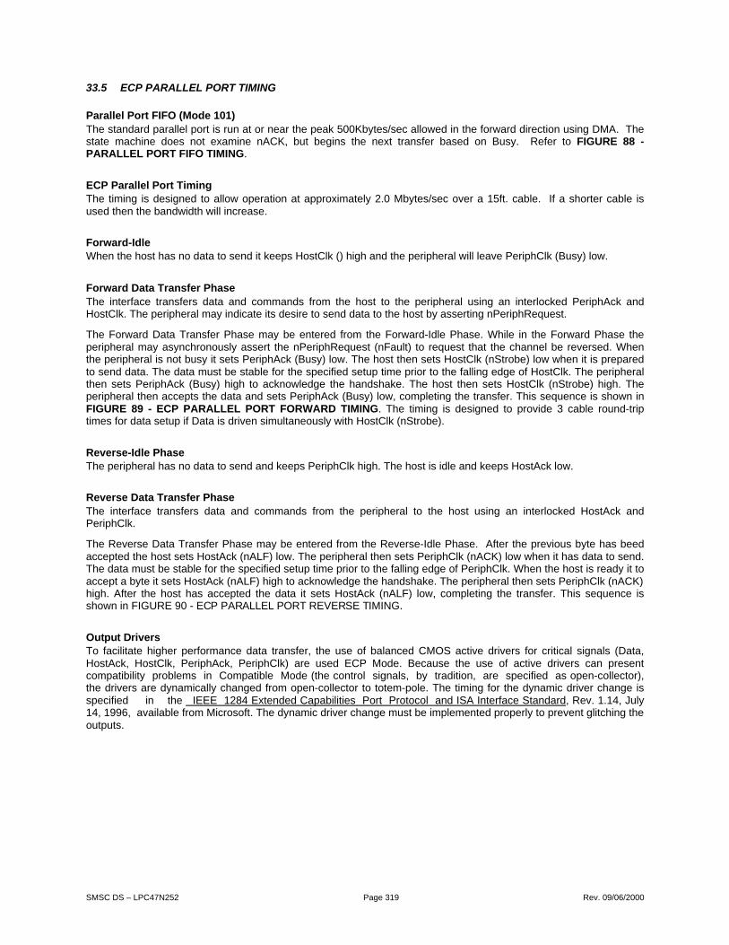
SMSC DS – LPC47N252 Page 319 Rev. 09/06/2000
33.5 ECP PARALLEL PORT TIMING
Parallel Port FIFO (Mode 101)The standard parallel port is run at or near the peak 500Kbytes/sec allowed in the forward direction using DMA. Thestate machine does not examine nACK, but begins the next transfer based on Busy. Refer to FIGURE 88 -PARALLEL PORT FIFO TIMING.
ECP Parallel Port TimingThe timing is designed to allow operation at approximately 2.0 Mbytes/sec over a 15ft. cable. If a shorter cable isused then the bandwidth will increase.
Forward-IdleWhen the host has no data to send it keeps HostClk () high and the peripheral will leave PeriphClk (Busy) low.
Forward Data Transfer PhaseThe interface transfers data and commands from the host to the peripheral using an interlocked PeriphAck andHostClk. The peripheral may indicate its desire to send data to the host by asserting nPeriphRequest.
The Forward Data Transfer Phase may be entered from the Forward-Idle Phase. While in the Forward Phase theperipheral may asynchronously assert the nPeriphRequest (nFault) to request that the channel be reversed. Whenthe peripheral is not busy it sets PeriphAck (Busy) low. The host then sets HostClk (nStrobe) low when it is preparedto send data. The data must be stable for the specified setup time prior to the falling edge of HostClk. The peripheralthen sets PeriphAck (Busy) high to acknowledge the handshake. The host then sets HostClk (nStrobe) high. Theperipheral then accepts the data and sets PeriphAck (Busy) low, completing the transfer. This sequence is shown inFIGURE 89 - ECP PARALLEL PORT FORWARD TIMING. The timing is designed to provide 3 cable round-triptimes for data setup if Data is driven simultaneously with HostClk (nStrobe).
Reverse-Idle PhaseThe peripheral has no data to send and keeps PeriphClk high. The host is idle and keeps HostAck low.
Reverse Data Transfer PhaseThe interface transfers data and commands from the peripheral to the host using an interlocked HostAck andPeriphClk.
The Reverse Data Transfer Phase may be entered from the Reverse-Idle Phase. After the previous byte has beedaccepted the host sets HostAck (nALF) low. The peripheral then sets PeriphClk (nACK) low when it has data to send.The data must be stable for the specified setup time prior to the falling edge of PeriphClk. When the host is ready it toaccept a byte it sets HostAck (nALF) high to acknowledge the handshake. The peripheral then sets PeriphClk (nACK)high. After the host has accepted the data it sets HostAck (nALF) low, completing the transfer. This sequence isshown in FIGURE 90 - EC P PAR ALLEL PORT REVER SE T IMING.
Out pu t D riversTo facilitate higher performance data transfer, the use of balanced CMOS active drivers for critical signals (Data,HostAck, HostClk, PeriphAck, PeriphClk) are used ECP Mode. Because the use of active drivers can presentcompatibility problems in Compatible Mode (the control signals, by tradition, are specified as open-collector),the drivers are dynamically changed from open-collector to totem-pole. The timing for the dynamic driver change isspecified in the IEEE 1284 Extended Capabilities Port Protocol and ISA Interface Standard, Rev. 1.14, July14, 1996, available from Microsoft. The dynamic driver change must be implemented properly to prevent glitching theoutputs.

SMSC DS – LPC47N252 Page 320 Rev. 09/06/2000
FIGURE 88 - PARALLEL PORT FIFO TIMING
N AM E D ESCR IPT ION M IN T YP M AX U NITS
t1 D AT A Val id to nSTR OBE Acti ve 600 ns
t2 nST ROBE Active Pul se Wi dth 600 ns
t3 D AT A H ol d from nST ROBE Inactive ( Note 1) 450 ns
t4 nST ROBE Active to BU SY Active 500 ns
t5 BUSY Inacti ve to nST R OBE Active 680 ns
t6 BUSY Inacti ve to PDAT A Inval id (N ote 1) 80 nsN ot e 1: T he data i s hel d unti l BU SY goes inactive or for ti me t3, whi chever is longer. T hi s onl y appli es if another datatransfer i s pending. If no other data tr ansfer is pendi ng, the data i s hel d i ndefi ni tel y.
t3
t6
t1 t2 t5
t4
PD<7:0>
nSTROBE
BUSY

SMSC DS – LPC47N252 Page 321 Rev. 09/06/2000
t3
t4
t1
t2
t7 t8
t6 t5 t6
nALF
PD<7:0>
BUSY
nSTROBE
FIGURE 89 - EC P PAR A LL EL PORT FORW A RD T IMING
N AM E D ESCR IPT ION M IN T YP M AX U NITS
t1 nALF Val id to nSTR OBE Asserted 0 60 ns
t2 PDATA Vali d to nST ROBE Asser ted 0 60 ns
t3 BUSY D easserted to nALF C hanged
( Notes 1,2)
80 180 ns
t4 BUSY D easserted to PD AT A C hanged (N otes 1,2) 80 180 ns
t5 nST ROBE Asser ted to Busy Asser ted 0 ns
t6 nST ROBE Deasser ted to Busy D easserted 0 ns
t7 BUSY D easserted to nSTR OBE Asserted (N otes 1,2) 80 200 ns
t8 BUSY Asser ted to nST R OBE D easserted (N ote 2) 80 180 ns
N ot e 1: M axim um val ue only appl ies i f there is data i n the FIFO waiti ng to be w ri tten out.N ot e 2: BUSY i s not consider ed asser ted or deasserted unti l i t i s stabl e for a mi ni m um of 75 to 130 ns.

SMSC DS – LPC47N252 Page 322 Rev. 09/06/2000
t2
t1
t5 t6
t4 t3 t4
PD<7:0>
nACK
nALF
FIGURE 90 - EC P PAR A LL EL PORT REVER SE T IMING
N AM E D ESCR IPT ION M IN T YP M AX U NITS
t1 PDATA Vali d to nAC K Asser ted 0 ns
t2 nALF D easserted to PD AT A C hanged 0 ns
t3 nAC K Asser ted to nALF D easserted( Notes 1,2)
80 200 ns
t4 nAC K D easserted to nALF Asserted (N ote 2) 80 200 ns
t5 nALF Asser ted to nAC K Asserted 0 ns
t6 nALF D easserted to nACK D easser ted 0 ns
N ot e 1: M axim um val ue only appl ies i f there is r oom i n the FIFO and ter mi nal count has not been recei ved. EC P canstall by keeping nALF l ow .
N ot e 2: nAC K i s not consider ed asser ted or deasserted unti l i t i s stabl e for a mi ni m um of 75 to 130 ns.

SMSC DS – LPC47N252 Page 323 Rev. 09/06/2000
33.6 SER IA L IRQ TIMIN G
t2t1
PCI_CLK
SER_IRQ
FIGURE 91 – SETUP AND HOLD TIME
NAME DESCRIPTION MIN TYP MAX UNITS
t1 SER_IRQ SETUP TIME TO PCI_CLK RISING 7 nsec
t2 SER_IRQ Hold Time to PCI_CLK Rising 0 nsec
33.7 SERIAL PORT DATA TIMING
Data (5-8 Bits)t1
Data
TXD1, 2
Start ParityStop (1-2 Bits)
FIGURE 92 – SERIAL PORT DATA
NAME DESCRIPTION MIN TYP MAX UNITS
t1 Serial Port Data Bit Time tBR1 nsec
Note 1: tBR is 1/Baud Rate. The Baud Rate is programmed through the divisor latch registers. Baud Rates havepercentage errors indicated in the “Baud Rate” table in the “Serial Port” section.

SMSC DS – LPC47N252 Page 324 Rev. 09/06/2000
33.8 ACCESS.BUS TIMING
tHD;STA
tSU;STOtSU;STAtSU;DATtHIGH
tFtRtLOW
tHD;DAT
tHD;STA
tBUF
AB_DATA
AB_CLK
FIGURE 93 - ACCESS.BUS TIMING
SYMBOL PARAMETER MIN. TYP. MAX. UNIT
fSCL SCL Clock Frequency 100 kHz
tBUF Bus Free Time 4.7 µs
tSU;STA START Condition Set-Up Time 4.7 µs
tHD;STA START Condition Hold Time 4.0 µs
tLOW SCL LOW Time 4.7 µs
tHIGH SCL HIGH Time 4.0 µs
tR SCL and SDA Rise Time 1.0 µs
tF SCL and SDA Fall Time 0.3 µs
tSU;DAT Data Set-Up Time 0.25 µs
tHD;DAT Data Hold Time 0 µs
tSU;STO STOP Condition Set-Up Time 4.0 µs

SMSC DS – LPC47N252 Page 325 Rev. 09/06/2000
33.9 FAN AND FAN TACHOMETER TIMING
t1t2
FANx
FIGURE 94 – FAN OUTPUT TIMING
NAME DESCRIPTION MIN TYP MAX UNITS
t1 PWM PERIOD (NOTE 1) 0.021 25.8 msec
t2 PWM HIGH TIME (NOTE 2) 0.00033 25.4 msecNote 1: The period is 1/fout,where fout is programmed through the PWMx and PWM Control registers. The toleranceon fout is +/- 5%.Note 2: When Bit 0 of the PWMx registers is 0, then the duty cycle is programmed through Bits[6:1] of theseregisters. If Bits[6:1] = “000000” then the PWMx pin is low. The duty cycle is programmable through Bits[6:1] to bebetween 1.56% and 98.44%. When Bit 0 is 1, the PWMx pin is high.
t3t1
t2FAN_TACHx
FIGURE 95 – FAN TACHOMETER INTPUT TIMING
NAME DESCRIPTION MIN TYP MAX UNITS
t1 PULSE TIME (1/2 REVOLUTIONTIME=30/RPM)
4TTACH1 µsec
t2 PULSE HIGH TIME 3TTACH1 µsec
t3 PULSE LOW TIME TTACH µsecNote 1: tTACH is the clock used for the tachometer counter. It is 30.52* prescaler, where the prescaler is programmedin the Fan Tachometer Timebase Prescaler register.

SMSC DS – LPC47N252 Page 326 Rev. 09/06/2000
33.10 PS/2 TIMING
t7
t2t2t3
t4t3
t4
t7
t5 t10 t11
t1 t6
t8 t9
t12
b7b0 b1 b2 b3 b4 b5 b6 P S
WR_CLK
WR_DATA
WR_C
WR_DA
note1
PS2_CLK
PS2_DAT
PS2_EN
PS2_T/R
RDATA_RDY
Read RX Reg
Interrupt
FIGURE 96 - PS/2 CHANNEL RECEIVE TIMING DIAGRAM
PARAMETER MIN TYP MAX UNITS
t1 The PS2 Channel’s CLK and DATA linesare floated following PS2_EN=1 andPS2_T/R=0.
100 ns
t2 Period of CLK 60 302 us
t3 Duration of CLK high (active) 30 151 us
t4 Duration of CLK low (inactive) 30 151 us
t5 DATA setup time to falling edge of CLK.LPC47N252 samples the data line on thefalling CLK edge.
1 us
t6 DATA hold time from falling edge of CLK.LPC47N252 samples the data line on thefalling CLK edge.
2 us
t7 Duration of Data Frame. Falling edge ofStart bit CLK (1st clk) to falling edge ofParity bit CLK (10th clk).
2.002 ms
t8 Falling edge of 11th CLK to RDATA_RDYasserted.
1.6 us
t9 Trailing edge of the 8051’s RD signal ofthe Receive Register to RDATA_RDY bitdeasserted.
100 ns
t10 Trailing edge of the 8051’s RD signal ofthe Receive Register to the CLK linereleased to high-Z.
100 ns
t11 The PS2 Channel’s CLK and DATA linesare driven to the values stored in theWR_CLK and WR_DATA bits of theControl Register when PS2_EN is writtento 0.
100 ns
t12 RDATA_RDY asserted to interruptgenerated. Note1- Interrupt is cleared byreading the 8051 INT0 Source Register.
100 ns

SMSC DS – LPC47N252 Page 327 Rev. 09/06/2000
t6t6
t10
t7t7t8t8
t9t9
t10
t2 t5
t1 t4 t11 t14 t16
t12
t3 t13
t15
Pb0 b1 b2 b3
ORION005
b4 b5 b6 b7S
1 211
note1
10PS2_CLK
PS2_DAT
PS2_EN
PS2_T/R
XMIT_IDLE
RDATA_RDY
Write TX Reg
Interrupt
FIGURE 97 - PS/2 CHANNEL TRANSMIT TIMING DIAGRAM
PS/2 CHANNEL TRANSMISSION TIMING PARAMETERSPARAMETER MIN TYP MAX UNITS
t1 The PS2 Channel’s CLK and DATA lines are floatedfollowing PS2_EN=1 and PS2_T/R=0.
100 ns
t2 PS2_T/R bit set to CLK driven low preparing the PS2Channel for data transmission.
100 ns
t3 CLK line floated to XMIT_IDLE bit deasserted. 1.7 us
t4 Trailing edge of 8051 WR of Transmit Register toDATA line driven low.
45 90 ns
t5 Trailing edge of 8051 WR of Transmit Register toCLK line floated.
90 130 ns
t6 Initiation of Start of Transmit cycle by the PS2channel controller to the auxilliary peripheral’sresponding by latching the Start bit and driving theCLK line low.
0.002 25.003 ms
t7 Period of CLK 60 302 us
t8 Duration of CLK high (active) 30 151 us
t9 Duration of CLK low (inactive) 30 151 us
t10 Duration of Data Frame. Falling edge of Start bit CLK(1st clk) to falling edge of Parity bit CLK (10th clk).
2.002 ms
t11 DATA output by LPC47N252 following the fallingedge of CLK. The auxilliary peripheral devicesamples DATA following the rising edge of CLK.
3.5 7.1 us
t12 Rising edge following the 11th falling clock edge toPS_T/R bit driven low.
400 800 ns
t13 Trailing edge of PS_T/R to XMIT_IDLE bit asserted. 100 ns
t14 DATA released to high-Z following the PS2_T/R bitgoing low.
100 ns

SMSC DS – LPC47N252 Page 328 Rev. 09/06/2000
PARAMETER MIN TYP MAX UNITS
t15 XMIT_IDLE bit driven high to interrupt generated.Note1- Interrupt is cleared by reading the 8051 INT0Source Register.
100 ns
t16 The PS2 Channel’s CLK and DATA lines are drivento the values stored in the WR_CLK and WR_DATAbits of the Control Register when PS2_EN is writtento 0.
100 ns
t1 t1
note1 note1
note2 note2
PS2_CLK1
PS2_DAT
Interrupt
PS2_EN
FIGURE 98 - PS/2 CHANNEL “BIT-BANG” TRANSMIT TIMING DIAGRAM
PS/2 CHANNEL “BIT-BANG” TRANSMIT TIMING PARAMETERSPARAMETER MIN TYP MAX UNITS
t1 Falling Edge of CLK to Interruptgenerated.
1.1 us
note1 8051 firmware responds to interrupt anddrives data line before rising edge ofPS2_CLK line.
note2 8051 firmware clears Interrupt byreading the 8051 INT0 Source Register.
t1 t1
note1 note1
note2 note2
PS2_CLK1
PS2_DAT
Interrupt
PS2_EN
FIGURE 99 - PS/2 CHANNEL “BIT-BANG” RECEIVE TIMING DIAGRAM
PS/2 CHANNEL “BIT-BANG” RECEIVE TIMING PARAMETERSPARAMETER MIN TYP MAX UNITS
t1 Falling Edge of CLK to Interruptgenerated.
100 ns
note1 8051 firmware responds to interruptand latches data line before risingedge of PS2_CLK line.
note2 8051 firmware clears Interrupt byreading the 8051 INT0 SourceRegister.
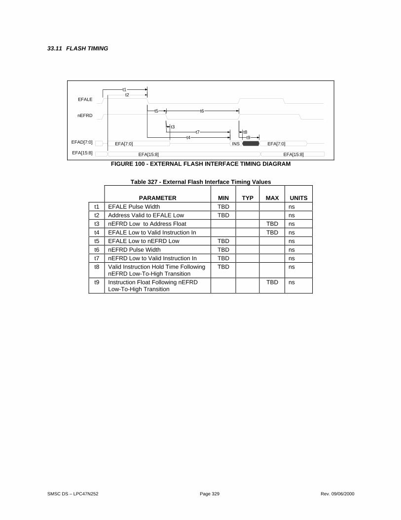
SMSC DS – LPC47N252 Page 329 Rev. 09/06/2000
33.11 FLASH TIMING
t2t1
t5 t6
t3
t4t7 t8
t9INSEFA[7:0] EFA[7:0]
EFA[15:8] EFA[15:8]
EFALE
nEFRD
EFAD[7:0]
EFA[15:8]
FIGURE 100 - EXTERNAL FLASH INTERFACE TIMING DIAGRAM
Table 327 - External Flash Interface Timing Values
PARAMETER MIN TYP MAX UNITS
t1 EFALE Pulse Width TBD ns
t2 Address Valid to EFALE Low TBD ns
t3 nEFRD Low to Address Float TBD ns
t4 EFALE Low to Valid Instruction In TBD ns
t5 EFALE Low to nEFRD Low TBD ns
t6 nEFRD Pulse Width TBD ns
t7 nEFRD Low to Valid Instruction In TBD ns
t8 Valid Instruction Hold Time FollowingnEFRD Low-To-High Transition
TBD ns
t9 Instruction Float Following nEFRDLow-To-High Transition
TBD ns

SMSC DS – LPC47N252 Page 330 Rev. 09/06/2000
34 PACKAGE OUTLINE DATA
AA1A2D
D1EE1H
MIN
0.05 1.3529.90
27.9029.9027.90 0.09
NOM
30.00
28.0030.0028.00
MAX 1.6 0.15 1.4530.10
28.1030.1028.100.230
NOM 0.60 1.00 0.50BSC
MIN0.45
00.170.080.08
MAX0.75
70.27
0.200.08
LL1e0WR1R2ccc
Notes:
1) Coplanarity is 0.080 mm or 3.2 mils maximum
2) Tolerance on the position of the leads is 0.080 mm maximum
3) Package body dimensions D1 and E1 do not include the mold protrusion.Maximum mold protrusion is 0.25 mm
5) Details of pin 1 identifier are optional but must be located within the zoneindicated
6) Controlling dimension: millimeter
4) Dimensions for foot length L measured at the gauge plane 0.25 mm abovethe seating plane
FIGURE 101 - 208 PIN TQFP PACKAGE OUTLINE

SMSC DS – LPC47N252 Page 331 Rev. 09/06/2000
FIGURE 102 - 208 PIN FL EX BGA 15.0X15.0X1.10 ( PRELIM IN AR Y)
MIN NOMINAL MAX REMARKA 1.0 1.1 1.2 Overall Package HeightA1 0.24 0.30 0.36 StandoffA2 0.76 0.80 0.84 Package Body ThicknessA3 0.32 0.35 0.38 Substrate ThicknessD 14.80 15.00 15.20 X Board LengthD1 12.70 12.80 12.90 X Distance Between End Ball CentersE 14.80 15.00 14.80 Y Board LengthE1 12.70 12.80 12.90 Y distance Between End Ball CentersF 29o 30o 31o Molded Lid AngleG 1.10 Typical X, Y Edge Distanceb 0.43 0.48 0.53 Ball Diametere 0.80 Typical Pitch
ccc 0.12 Maximum Coplanarity Notes:1 Contr ol li ng Uni t: m i ll im eter2 Toler ance on the position of the ball i s +/- 0.15 mm m axi mum .3 A1 ball pad cor ner m ust be located in zone i ndi cated.

SMSC DS – LPC47N252 Page 332 Rev. 09/06/2000
APPENDIX A: HIGH-PERFORMANCE 8051 CYCLE TIMING & INSTRUCTION SET
The high-performance 8051 processor offers increased performance by executing instructions in a 4-clock cycle, asopposed to the standard 8051. The shortened bus timing improves the instruction execution rate for mostinstructions by a factor of three over the standard 8051 architectutres.
Some instructions require a different number of instruction cycles on the high-performance 8051than they do on thestandard 8051. In the standard 8051, all instructions except for MUL and DIV take one or two instruction cycles tocomplete. Int the high-performance 8051 architecture, instructions can take between one and five instructions tocomplete. The average speed improvement for the entire instruction set is approximately 2.5X.
Legend For Instruction Set TableSYMBOL FUNCTION
A Accumulator
Rn Register R7-R0
direct Internal register address
@Ri Internal register pointed to by R0 or R1 (except MOVX)
rel Two’s complement offset byte
bit Direct bit address
#data 8-bit constant
#data 16 16-bit constant
addr 16 16-bit destination address
addr 11 11-bit destination address
Table 328 - 8051 Instruction Set
INSTRUCTION DESCRIPTIONBYTE
COUNTINSTRUCTION
CYCLESHEX
CODE
ARITHMETIC
ADD A, Rn Add register to A 1 1 28-2F
ADD A, direct Add direct byte to A 2 2 25
ADD A, @Ri Add data memory to A 1 1 26-27
ADD A, #data Add immediate to A 2 2 24
ADDC A, Rn Add register to A withcarry
1 1 38-3F
ADDC A, direct Add direct byte to A withcarry
2 2 35
ADDC A, @Ri Add data memory to Awith carry
1 1 36-37
ADDC A,#data
Add immediate to A withcarry
2 2 34
SUBB A, Rn Subtract register from Awith borrow
1 1 98-9F
SUBB A, direct Subtract direct byte fromA with borrow
2 2 95
SUBB A, @Ri Subtract data memoryfrom A with borrow
1 1 96-97
SUBB A, #data Subtract immediate fromA with borrow
2 2 94
INC A Increment A 1 1 04
INC Rn Increment register 1 1 08-0F
INC direct Increment direct byte 2 2 05
INC @Ri Increment data memory 1 1 06-07
DEC A Decrement A 1 1 14
DEC Rn Decrement register 1 1 18-1F
DEC direct Decrement direct byte 2 2 15
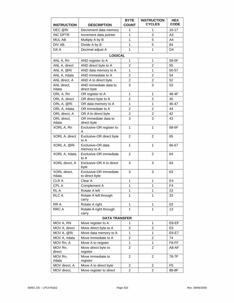
SMSC DS – LPC47N252 Page 333 Rev. 09/06/2000
INSTRUCTION DESCRIPTIONBYTE
COUNTINSTRUCTION
CYCLESHEX
CODE
DEC @Ri Decrement data memory 1 1 16-17
INC DPTR Increment data pointer 1 3 A3
MUL AB Multiply A by B 1 5 A4
DIV AB Divide A by B 1 5 84
DA A Decimal adjust A 1 1 D4
LOGICAL
ANL A, Rn AND register to A 1 1 58-5F
ANL A, direct AND direct byte to A 2 2 55
ANL A, @Ri AND data memory to A 1 1 56-57
ANL A, #data AND immediate to A 2 2 54
ANL direct, A AND A to direct byte 2 2 52
ANL direct,#data
AND immediate data todirect byte
3 3 53
ORL A, Rn OR register to A 1 1 48-4F
ORL A, direct OR direct byte to A 2 2 45
ORL A, @Ri OR data memory to A 1 1 46-47
ORL A, #data OR immediate to A 2 2 44
ORL direct, A OR A to direct byte 2 2 42
ORL direct,#data
OR immediate data todirect byte
3 3 43
XORL A, Rn Exclusive-OR register toA
1 1 68-6F
XORL A, direct Exclusive-OR direct byteto A
2 2 65
XORL A, @Ri Exclusive-OR datamemory to A
1 1 66-67
XORL A, #data Exclusive-OR immediateto A
2 2 64
XORL direct, A Exclusive-OR A to directbyte
3 3 63
XORL direct,#data
Exclusive-OR immediateto direct byte
3 3 63
CLR A Clear A 1 1 E4
CPL A Complement A 1 1 F4
RL A Rotate A left 1 1 23
RLC A Rotate A left throughcarry
1 1 33
RR A Rotate A right 1 1 03
RRC A Rotate A right throughcarry
1 1 13
DATA TRANSFER
MOV A, RN Move register to A 1 1 E8-EF
MOV A, direct Move direct byte to A 2 2 E5
MOV A, @Ri Move data memory to A 1 1 E6-E7
MOV A, #data Move immediate to A 2 2 74
MOV Rn, A Move A to reigster 1 1 F8-FF
MOV Rn,direct
Move direct byte toregister
2 2 A8-AF
MOV Rn,#data
Move immediate toregister
2 2 78-7F
MOV direct, A Move A to direct byte 2 2 F5
MOV direct, Move register to direct 2 2 88-8F

SMSC DS – LPC47N252 Page 334 Rev. 09/06/2000
INSTRUCTION DESCRIPTIONBYTE
COUNTINSTRUCTION
CYCLESHEX
CODE
Rn byte
MOV direct,direct
Move direct byte todirect byte
3 3 85
MOV direct,@Ri
Move data memory todirect byte
2 2 86-87
MOV direct,#data
Move immediate todirect byte
3 3 75
MOV @Ri, A Move A to data memory 1 1 F6-F7
MOV @Ri,direct
Move direct byte to datamemory
2 2 A6-A7
MOV @Ri,#data
Move immediate to datamemory
2 2 76-77
MOV DPTR,#data
Move immediate to datapointer
3 3 90
MOVC A,@A+DPTR
Move code byte relativeDPTR to A
1 3 93
MOVC A,@A+PC
Move code byte relativePC to A
1 3 83
MOVX A, @Ri Move external data (A8)to A
1 2-9 E2-E3
MOVX A,@DPTR
Move external data(A16) to A
1 2-9 E0
MOVX @Ri, A Move A to external data(A8)
1 2-9 F2-F3
MOVX@DPTR, A
Move A to external data(A16)
1 2-9 F0
PUSH direct Push direct byte ontostack
2 2 C0
POP direct Pop direct byte fromstack
2 2 D0
XCH A, Rn Exchange A and register 1 1 C8-CF
XCH A, direct Exchange A and directbyte
2 2 C5
XCH A, @Ri Exchange A and datamemory
1 1 C6-C7
XCHD A, @Ri Exchange A and datamemory nibble
1 1 D6-D7
BOOLEAN
CLR C Clear carry 1 1 C3
CLR bit Clear direct bit 2 2 C2
SETB C Set Carry 1 1 D3
SETB bit Set direct bit 2 2 D2
CPL C Complement carry 1 1 B3
CPL bit Complement direct bit 2 2 B2
ANL C, bit AND direct bit to carry 2 2 82
ANL C, /bit AND direct bit inverse tocarry
2 2 B0
ORL C, bit OR direct bit to carry 2 2 72
ORL C, /bit OR direct bit inverse tocarry
2 2 A0
MOV C, bit Move direct bit to carry 2 2 A2
MOV bit, C Move carry to direct bit 2 2 92
BRANCHING
ACALL addr Absolute call to 2 3 11-F1

SMSC DS – LPC47N252 Page 335 Rev. 09/06/2000
INSTRUCTION DESCRIPTIONBYTE
COUNTINSTRUCTION
CYCLESHEX
CODE
11 subroutine
LCALL addr 16 Long call to subroutine 3 4 12
RET Return from subroutine 1 4 22
RETI Return from interrupt 1 4 32
AJMP addr 11 Absolute jumpunconditional
2 3 01-E1
LJMP addr 16 Long jump unconditional 3 4 02
SJMP rel Short jump (relativeaddress)
2 3 80
JC rel Jump on carry = 1 2 3 40
JNC rel Jump on carry = 0 2 3 50
JB bit, rel Jump on direct bit = 1 3 4 20
JNB bit, rel Jump on direct bit = 0 3 4 30
JMP@A+DPTR
Jump indirect relativeDPTR
1 3 73
JZ rel Jump on accumulator =0
2 3 60
JNZ rel Jump on accumulator /=0
2 3 70
CJNE A,direct, rel
Compare A, direct JNErelative
3 4 B5
CJNE A, #d,rel
Compare A, immediateJNE relative
3 4 B4
CJNE Rn, #d,rel
Compare reg, immediateJNE relative
3 4 B8-BF
CJNE @Ri, #d,rel
Compare Ind, immediateJNE relative
3 4 B6-B7
DJNZ Rn, rel Decrement register, JNZrelative
2 3 D8-DF
DJNZ direct,rel
Decrement direct byte,JNZ relative
3 4 D5
MISCELLANEOUS
NOP No operation 1 1 00

SMSC DS – LPC47N252 Page 336 Rev. 09/06/2000
APPENDIX B HIGH PERFORMANCE 8051 EXTENDED INTERRUPT UNIT
APPENDIX B INTERRUPTS
The EXIF, EICON, EIE, and EIP registers provide flags, enable control, and priority control for the extended interruptunit in the LPC47N252 high-performance 8051.
INTERRUPT PROCESSING
When an enabled interrupt occurs, the CPU vectors to the address of the interrupt service routine (ISR) associatedwith that interrupt (See Table 108 – 8051 Interrupts). The CPU executes the ISR to completion unless anotherinterrupt of higher priority occurs. Each ISR ends with a RETI (return from interrupt) instruction. After executing theRETI, the CPU returns to the next instruction that would have been executed if the interrupt had not occurred.
An ISR can only be interrupted by a higher priority interrupt. That is, an ISR for a low-level interrupt can only beinterrupted by high-level interrupt. An ISR for a high-level interrupt can only be interrupted by the power-fail interrupt(extended interrupt unit only).
The 8051 always completes the instruction in progress before servicing an interrupt. If the instruction in progress isRETI, or a write access to any of the IP, IE, EIP, or EIE SFRs, the 8051 completes one additional instruction beforeservicing the interrupt.
INTERRUPT MASKING
The EA bit in the IE SFR (IE.7) is a global enable for all interrupts except the power-fail interrupt. When EA = 1, eachinterrupt is enabled/masked by its individual enable bit. When EA = 0, all interrupts are masked. The only exception isthe power-fail interrupt, which is not affected by the EA bit. When EPFI = 1, the power-fail interrupt is enabled,regardless of the state of the EA bit. TABLE 92 on page 169 provides a summary of interrupt sources, flags, enables,and priorities.
INTERRUPT PRIORITIES
There are two stages of interrupt priority assignment, interrupt level and natural priority. The interrupt level (highest,high, or low) takes precedence over natural priority. The power-fail interrupt, if enabled, always has highest priorityand is the only interrupt that can have highest priority. All other interrupts can be assigned either high or low priority.In addition to an assigned priority level (high or low), each interrupt also has a natural priority, as listed in TABLE 92 -on page 169. Simultaneous interrupts with the same priority level (for example, both high) are resolved according totheir natural priority. For example, if int0_n and int2 are both programmed as high priority, int0_n takes precedence.Once an interrupt is being serviced, only an interrupt of higher priority level can interrupt the service routine of theinterrupt currently being serviced.
INTERRUPT SAMPLING
The internal timers and serial ports generate interrupts by setting their respective SFR interrupt flag bits. Externalinterrupts are sampled once per instruction cycle.int0_n and int1_n are both active low and can be programmed to be either edge-sensitive or level-sensitive, throughthe IT0 and IT1 bits in the TCON SFR. For example, when IT0 = 0, int0_n is level-sensitive and the 8051 sets the IE0flag when the int0_n pin is sampled low. When IT0 = 1, int0_n is edge-sensitive and 8051 sets the IE0 flag when theint0_n pin is sampled high then low on consecutive samples.The remaining four external interrupts are edge-sensitive only. int2 and int4 are active high, int3_n and int5_n areactive low. The power-fail (pfi) interrupt is edge-sensitive, active high, and sampled once per instruction cycle. Toensure that edge-sensitive interrupts are detected, the corresponding ports should be held high for 4 clk cycles andthen low for 4 clk cycles. Level-sensitive interrupts are not latched and must remain active until serviced.
INTERRUPT LATENCY
Interrupt response time depends on the current state of the 8051. The fastest response time is 5 instruction cycles: 1to detect the interrupt, and 4 to perform the LCALL to the ISR. The maximum latency (13 instruction cycles) occurswhen the 8051 is currently executing a RETI instruction followed by a MUL or DIV instruction. The 13 instructioncycles in this case are: 1 to detect the interrupt, 3 to complete the RETI, 5 to execute the DIV or MUL, and 4 toexecute the LCALL to the ISR. For the maximum latency case, the response time is 13 x 4 = 52 clk cycles.
DUAL DATA POINTERS
The high-performance 8051 in the LPC47N252 employs dual data pointers to accelerate data memory block moves.The standard 8051 data pointer (DPTR) is a 16-bit value used to address external RAM or peripherals. TheLPC47N252 maintains the standard data pointer as DPTR0 at SFR locations 82h and 83h. It is not necessary tomodify code to use DPTR0.

SMSC DS – LPC47N252 Page 337 Rev. 09/06/2000
The LPC47N252 adds a second data pointer (DPTR1) at SFR locations 84h and 85h. The SEL bit in the DPTRSelect Register, DPS (SFR 86h), selects the active pointer (see sections DPL1, DPH1 and DPS below).All DPTR-related instructions use the currently selected data pointer. To switch the active pointer, toggle the SEL bit.The fastest way to do so is to use the increment instruction (INC DPS). This requires only one instruction to switchfrom a source address to a destination address, saving application code from having to save source and destinationaddresses when doing a block move.
TIMER 2
OVERVIEW
The high-performance 8051 in the LPC47N252 includes a third timer/counter (Timer 2). Timer 2 runs only in 16-bitmode and offers several capabilities not available with Timers 0 and 1. The modes available with Timer 2 are 16-bitauto-reload timer/counter and baud rate generator. The SFRs associated with Timer 2 are:T2CON (SFR C8h)RCAP2L (SFR CAh) – Used as the 16-bit LSB reload value when Timer 2 is configured for auto-reload mode.RCAP2H (SFR CBh) – Used as the 16-bit MSB reload value when Timer 2 is configured for auto-reload mode.TL2 (SFR CCh) – Lower 8 bits Table 332-bit count.TH2 (SFR CDh) – Upper 8 bits of 16-bit count.
Table 329 summarizes how the T2CON SFR bits (Table 333) determine the Timer 2 operating mode.
Table 329 - Timer 2 Mode Control Summary
RCLK TCLK TR2 MODE
0 0 1 16-bit Timer/Counter w/Auto-reload
1 X 1 Baud Rate Generator
X 1 1 Baud Rate Generator
X X 0 Off
16-BIT TIMER/COUNTER MODE WITH AUTO-RELOAD
FIGURE 103 illustrates how Timer 2 operates in timer/counter mode with auto-reload. The 16-bit timer counts CLKcycles (divided by 4 or 12). The TR2 bit enables the counter. When the count increments from FFFFh, the overflowoccurs. The overflow causes the TF2 flag is set, and t2_out goes high for one CLK cycle. The overflow also causesthe preloaded start value in the RCAP2L and RCAP2H registers to be reloaded into the TL2 and TH2 registers.
DIVIDE BY 12
DIVIDE BY 4
CLK
TR2
T2M
TL2 TH2
RCAP2L RCAP2H
clk
TF2 INT
0
1
FIGURE 103 - TIMER 2 TIMER/COUNTER WITH AUTO-RELOAD
BAUD RATE GENERATOR MODE
Setting either RCLK or TCLK to 1 configures Timer 2 to generate baud rates for Serial Port 0 in serial mode 1 or 3. Inbaud rate generator mode, Timer 2 functions in auto-reload mode. However, instead of setting the TF2 flag, thecounter overflow is used to generate a shift clock for the serial port function. As in normal auto-reload mode, theoverflow also causes the preloaded start value in the RCAP2L and RCAP2H registers to be reloaded into the TL2and TH2 registers.When either TCLK = 1 or RCLK = 1, Timer 2 is forced into auto-reload operation. The counter time base in baud rategenerator mode is clk/2.
SPECIAL FUNCTION REGISTERS
The following SFRs are not part of the sandard 8051 architecture.

SMSC DS – LPC47N252 Page 338 Rev. 09/06/2000
DPL1
The DPL1 register (Table 330) is the LSB of DPTR1
Table 330 - DPL1 Register - SFR 84HSFR ADDRESS 84h
POWER VCC1
DEFAULT 0x00
D7 D6 D5 D4 D3 D2 D1 D0
TYPE R/W R/W R/W R/W R/W R/W
R/W R/W
BIT NAME A7 A6 A5 A4 A3 A2 A1 A0
DPH1The DPH1 register (Table 331) is the MSB of DPTR1
Table 331 - DPH1 Register - SFR 85HSFR ADDRESS 85h
POWER VCC1
DEFAULT 0x00
D7 D6 D5 D4 D3 D2 D1 D0
TYPE R/W R/W R/W R/W R/W R/W R/W R/W
BIT NAME A15 A14 A13 A12 A11 A10 A9 A8
DPSThe DPS register (Table 332) is used to select the active DPTR
Table 332 - DPS Register - SFR 86hSFR ADDRESS 86h
POWER VCC1
DEFAULT 0x00
D7 D6 D5 D4 D3 D2 D1 D0
TYPE R R R R R R R R/W
BIT NAME RESERVED SEL1
Note1: When SEL = ‘0’, instructions that use the DPTR will use DPL0 and DPH0. When SEL = ‘1’, instructions thatuse the DPTR will use DPL1 and DPH1.
CKCON
The default timer clock scheme for the DW8051 timers is 12 clk cycles per increment, the same as in the standard8051. However, in the DW8051, the instruction cycle is 4 clk cycles. Using the default rate (12 clocks per timerincrement) allows existing application code with real-time dependencies, such as baud rate, to operate properly.However, applications that require fast timing can set the timers to increment every 4 clk cycles by setting bits in theClock Control register (CKCON) at SFR location 8Eh (Table 333 and Table 334)
The CKCON bits that control the timer clock rates are:
CKCON BIT COUNTER/TIMER5 Timer 24 Timer 13 Timer 0
When a CKCON register bit is set to 1, the associated counter increments at 4-clk intervals. When a CKCON bit iscleared, the associated counter increments at 12-clk intervals. The timer controls are independent of each other. Thedefault setting for all three timers is 0 (12-clk intervals). These bits have no effect in counter mode.

SMSC DS – LPC47N252 Page 339 Rev. 09/06/2000
Table 333 - CKCON Register - SFR 8EHSFR ADDRESS 8EH
POWER VCC1
DEFAULT 0x01
D7 D6 D5 D4 D3 D2 D1 D0
TYPE R R R/W R/W R/W R/W R/W R/W
BIT NAME RESERVED T2M T1M T0M MD2 MD1 MD0
Table 334 - CKCON Register Bit DescriptionsBIT FUNCTION
CKCON.7-6 Reserved
CKCON.5 T2M. Timer 2 clock select. When T2M = 0, Timer 2 usesclk/12 (for compatibility with 80C32); when T2M = 1, Timer 2uses clk/4. This bit has no effect when Timer 2 is configuredfor baud rate generation.
CKCON.4 T1M. Timer 1 clock select. When T1M = 0, Timer 1 usesclk/12 (for compatibility with 80C32); when T1M = 1, Timer 1uses clk/4.
CKCON.3 T0M. Timer 0 clock select. When T0M = 0, Timer 0 usesclk/12 (for compatibility with 80C32); when T0M = 1, Timer 0uses clk/4.
CKCON.2-0 MD2, MD1, MD0 -- Control the number of cycles to be usedfor external MOVX instructions.
MPAGE
The MPAGE special function register (Table 335) replaces the function of the Port 2 latch in the LPC47N252. DuringMOVX A, @Ri and MOVX @Ri, A instructions, the 8051 places the contents of the MPAGE register on the uppereight address bits. This provides the paging function that is normally provided by the Port 2 latch.
Table 335 - Mpage Register – SFR 92HSFR ADDRESS 92H
POWER VCC1
DEFAULT 0x00
D7 D6 D5 D4 D3 D2 D1 D0
TYPE R/W R/W R/W R/W R/W R/W R/W R/W
BIT NAME A15 A14 A13 A12 A11 A10 A9 A8
T2CON
The T2CON register Table 336 and Table 337 is used to configure Timer 2
Table 336 – T2CON Register - SFR C8HSFR ADDRESS C8h
POWER VCC1
DEFAULT 0x00
D7 D6 D5 D4 D3 D2 D1 D0
TYPE R/W R/W R/W R/W R/W R/W R/W R/W
BIT NAME TF2 RESERVED RCLK TCLK RESERVED TR2 RESERVED

SMSC DS – LPC47N252 Page 340 Rev. 09/06/2000
Table 337 – T2CON Register Bit DescriptionsBIT FUNCTION
T2CON.7 TF2 Timer 2 overflow flag. Hardware will set TF2 when theTimer 2 overflows from FFFFh. TF2 must be cleared to 0 bythe software. TF2 will only be set to a 1 if RCLK and TCLKare both cleared to 0. Writing a 1 to TF2 forces a Timer 2interrupt if enabled.
T2CON.6 Reserved. This bit should be written as ‘0’.
T2CON.5 RCLK Receive clock flag. Determines whether Timer 1 orTimer 2 is used for Serial Port 0 timing of received data inserial mode 1 or 3. RCLK =1 selects Timer 2 overflow as thereceive clock. RCLK =0 selects Timer 1 overflow as thereceive clock.
T2CON.4 TCLK Transmit clock flag. Determines whether Timer 1 orTimer 2 is used for Serial Port 0 timing of transmit data inserial mode 1 or 3. RCLK =1 selects Timer 2 overflow as thetransmit clock. RCLK =0 selects Timer 1 overflow as thetransmit clock.
T2CON.3 Reserved. This bit should be written as ‘0’.
T2CON.2 TR2. Timer 2 run control flag. TR2 = 1 starts Timer 2. TR2= 0 stops Timer 2.
T2CON.1-0 Reserved. This bit should be written as ‘0’.
RCAP2L
The RCAP2L registerTable 338 is the 16-bit LSB reload value (RV[7:0]) when Timer 2 is configured for auto-reload mode.
Table 338 - RCAP2l Register – SFR CAHSFR ADDRESS CAh
POWER VCC1
DEFAULT 0x00
D7 D6 D5 D4 D3 D2 D1 D0
TYPE R/W R/W R/W R/W R/W R/W R/W R/W
BIT NAME RV7 RV6 RV5 RV4 RV3 RV2 RV1 RV0
RCAP2H
The RCAP2H registerTable 339 is the 16-bit MSB reload value (RV[15:8]) when Timer 2 is configured for auto-reload mode.
Table 339 - RCAP2H Register - SFR CBHSFR ADDRESS CBh
POWER VCC1
DEFAULT 0x00
D7 D6 D5 D4 D3 D2 D1 D0
TYPE R/W R/W R/W R/W R/W R/W R/W R/W
BIT NAME RV15 RV14 RV13 RV12 RV11 RV10 RV9 RV8

SMSC DS – LPC47N252 Page 341 Rev. 09/06/2000
TL2
The TL2 register (Table 340) is the 16-bit LSB Timer 2 count value (CV[7:0]).
Table 340 - Tl2 Register - SFR CCHSFR ADDRESS CCh
POWER VCC1
DEFAULT 0x00
D7 D6 D5 D4 D3 D2 D1 D0
TYPE R/W R/W R/W R/W R/W R/W R/W R/W
BIT NAME CV7 CV6 CV5 CV4 CV3 CV2 CV1 CV0
TH2
The TH2 register (Table 341) is the 16-bit MSB Timer 2 count value (CV[15:8]).
Table 341 - TH2 Register - SFR CDHSFR ADDRESS CDh
POWER VCC1
DEFAULT 0x00
D7 D6 D5 D4 D3 D2 D1 D0
TYPE R/W R/W R/W R/W R/W R/W R/W R/W
BIT NAME CV15 CV14 CV13 CV12 CV11 CV10 CV9 CV8
EXIF
The EXIF registerTable 342 and Table 343 contains the external interrupt flags for the extended interrupt unit.
Table 342 - EXIF Register - SFR 91HSFR ADDRESS 91h
POWER VCC1
DEFAULT 0x08
D7 D6 D5 D4 D3 D2 D1 D0
TYPE R/W R/W R/W R/W R R R R
BIT NAME IE5 IE4 IE3 IE2 RESERVED

SMSC DS – LPC47N252 Page 342 Rev. 09/06/2000
Table 343 - EXIF Register Bit DescriptionsBIT FUNCTION
EXIF.7 IE5 External Interrupt 5 flag. IE5 = 1 indicates a falling edgewas detected at the int5_n pin. IE5 must be cleared bysoftware. Setting IE5 in software generates an interrupt, ifenabled.
EXIF.6 IE4 External Interrupt 4 flag. IE4 = 1 indicates a rising edgewas detected at the int4 pin. IE4 must be cleared bysoftware. Setting IE4 in software generates an interrupt, ifenabled.
EXIF.5 IE3 External Interrupt 3 flag. IE3 = 1 indicates a falling edgewas detected at the int3_n pin. IE3 must be cleared bysoftware. Setting IE3 in software generates an interrupt, ifenabled.
EXIF.4 IE2 External Interrupt 2 flag. IE2 = 1 indicates a rising edgewas detected at the int2 pin. IE2 must be cleared bysoftware. Setting IE2 in software generates an interrupt, ifenabled.
EXIF.3 Reserved. Read as ‘1’.
EXIF.2-0 Reserved. Read as ‘0’.
EICON
The EICON registerTable 344 and Table 345 contains pfi and serial port 1 controls for the extended interrupt unit.
Table 344 - EICON Register - SFR D8HSFR ADDRESS D8h
POWER VCC1
DEFAULT 0x40
D7 D6 D5 D4 D3 D2 D1 D0
TYPE R/W R/W R/W R/W R R R R
BIT NAME SMOD1 RESERVED EPFI PFI RESERVED
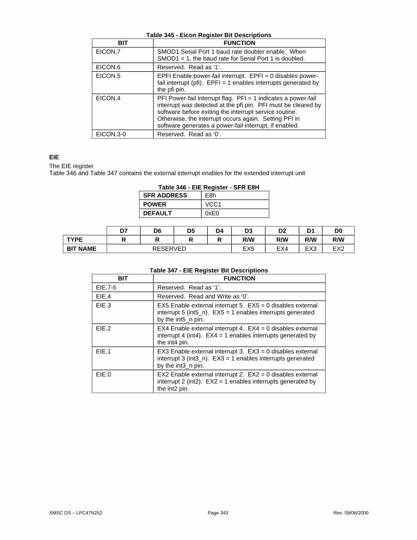
SMSC DS – LPC47N252 Page 343 Rev. 09/06/2000
Table 345 - Eicon Register Bit DescriptionsBIT FUNCTION
EICON.7 SMOD1 Serial Port 1 baud rate doubler enable. WhenSMOD1 = 1, the baud rate for Serial Port 1 is doubled.
EICON.6 Reserved. Read as ‘1’.
EICON.5 EPFI Enable power-fail interrupt. EPFI = 0 disables power-fail interrupt (pfi). EPFI = 1 enables interrupts generated bythe pfi pin.
EICON.4 PFI Power-fail interrupt flag. PFI = 1 indicates a power-failinterrupt was detected at the pfi pin. PFI must be cleared bysoftware before exiting the interrupt service routine.Otherwise, the interrupt occurs again. Setting PFI insoftware generates a power-fail interrupt, if enabled.
EICON.3-0 Reserved. Read as ‘0’.
EIE
The EIE registerTable 346 and Table 347 contains the external interrupt enables for the extended interrupt unit
Table 346 - EIE Register - SFR E8HSFR ADDRESS E8h
POWER VCC1
DEFAULT 0xE0
D7 D6 D5 D4 D3 D2 D1 D0
TYPE R R R R R/W R/W R/W R/W
BIT NAME RESERVED EX5 EX4 EX3 EX2
Table 347 - EIE Register Bit DescriptionsBIT FUNCTION
EIE.7-5 Reserved. Read as ‘1’.
EIE.4 Reserved. Read and Write as ‘0’.
EIE.3 EX5 Enable external interrupt 5. EX5 = 0 disables externalinterrupt 5 (int5_n). EX5 = 1 enables interrupts generatedby the int5_n pin.
EIE.2 EX4 Enable external interrupt 4. EX4 = 0 disables externalinterrupt 4 (int4). EX4 = 1 enables interrupts generated bythe int4 pin.
EIE.1 EX3 Enable external interrupt 3. EX3 = 0 disables externalinterrupt 3 (int3_n). EX3 = 1 enables interrupts generatedby the int3_n pin.
EIE.0 EX2 Enable external interrupt 2. EX2 = 0 disables externalinterrupt 2 (int2). EX2 = 1 enables interrupts generated bythe int2 pin.

SMSC DS – LPC47N252 Page 344 Rev. 09/06/2000
EIP
The EIP registerTable 348 and Table 349 contains the external interrupt priority controls for the extended interrupt unit.
Table 348 - EIP Register - SFR F8HSFR ADDRESS F8h
POWER VCC1
DEFAULT 0xE0
D7 D6 D5 D4 D3 D2 D1 D0
TYPE R R R R R/W R/W R/W R/W
BIT NAME RESERVED PX5 PX4 PX3 PX2
Table 349 - EIP Register Bit DescriptionsBIT FUNCTION
EIP.7-5 Reserved. Read as ‘1’.
EIP.4 Reserved. Read and Write as ‘0’.
EIP.3 PX5 External interrupt 5 priority control. PX5 = 0 setsexternal interrupt 5 (int5_n) to low priority. PX5 = 1 setsexternal interrupt 5 to high priority.
EIP.2 PX4 External interrupt 4 priority control. PX4 = 0 setsexternal interrupt 4 (int4) to low priority. PX2 = 1 setsexternal interrupt 4 to high priority.
EIP.1 PX3 External interrupt 3 priority control. PX3 = 0 setsexternal interrupt 3 (int3_n) to low priority. PX3 = 1 setsexternal interrupt 3 to high priority.
EIP.0 PX2 External interrupt 2 priority control. PX2 = 0 setsexternal interrupt 2 (int2) to low priority. PX2 = 1 setsexternal interrupt 2 to high priority.