Embed Size (px)
Citation preview
Low-‐Power Processors & New Memory Technologies
Chris&na Delimitrou
h1p://cs316.stanford.edu
CS316 – Fall 2014 – Lecture 15

2
Announcements
n Reading n Lecture notes + papers
n Reminders n HW2 (due today) n Project (progress report due on Wednesday)
n Exam: Thursday 11/20th, Lathrop 299, 3pm-‐6pm n All lectures and required reading un&l Monday 11/17 n Let us know early about alternate exam (+/-‐ 1 day of exam)
3
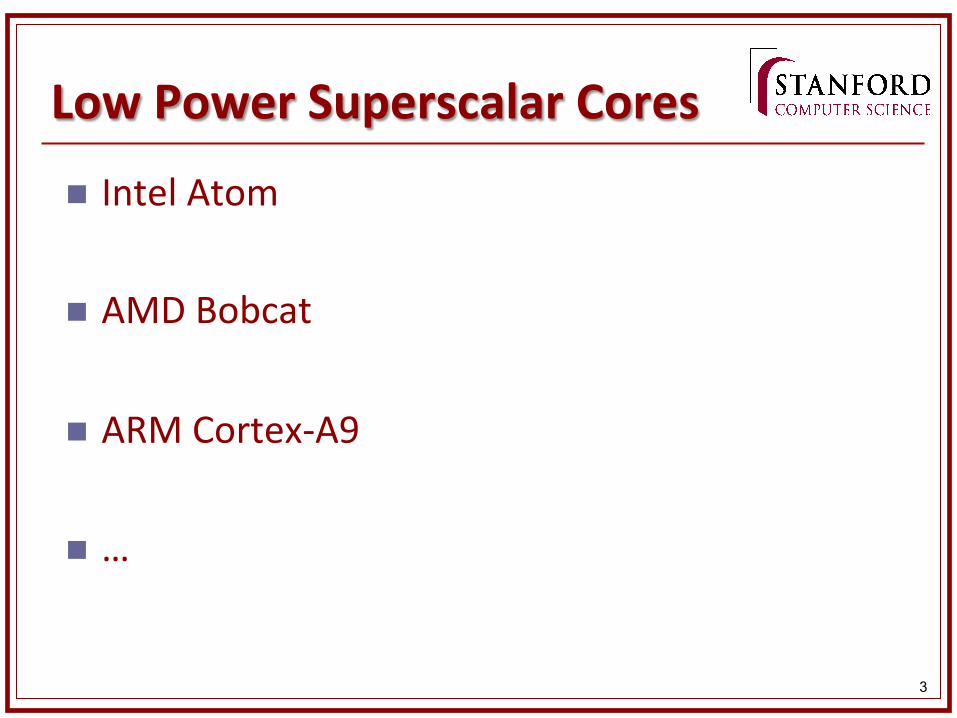
Low Power Superscalar Cores
n Intel Atom n AMD Bobcat
n ARM Cortex-‐A9
n …
4
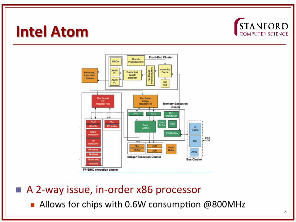
Intel Atom
n A 2-‐way issue, in-‐order x86 processor n Allows for chips with 0.6W consump&on @800MHz
5
Atom Design Decisions n 2-‐way threaded for u&liza&on/latency reasons n In-‐order pipeline with 16 stages
n Got rid of scheduling and reordering logic n Somewhat long pipeline to accommodate threads
n Simpler front-‐end n Avoid breaking up x86 ops to many micro-‐ops
n Few func&onal units to avoid waste n Loop cache: avoid fetching/decoding small loops n Large cache to avoid misses
n Cache designed to reduce leakage
6
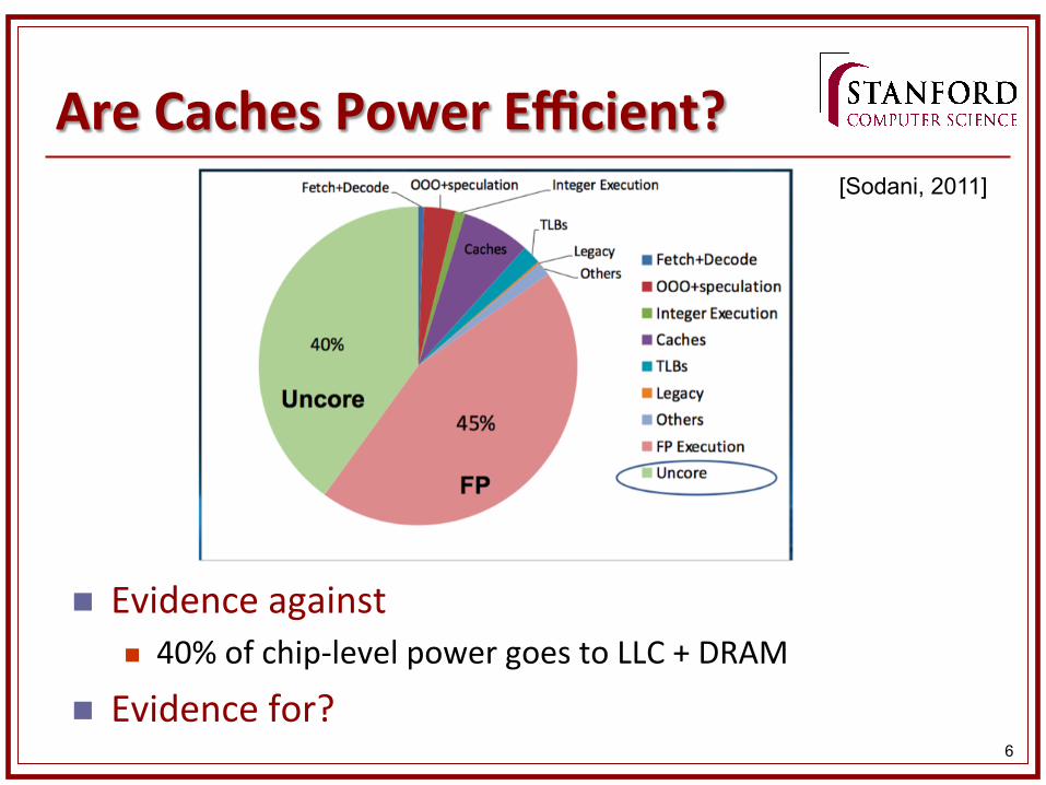
Are Caches Power Efficient?
n Evidence against n 40% of chip-‐level power goes to LLC + DRAM
n Evidence for?
[Sodani, 2011]
7
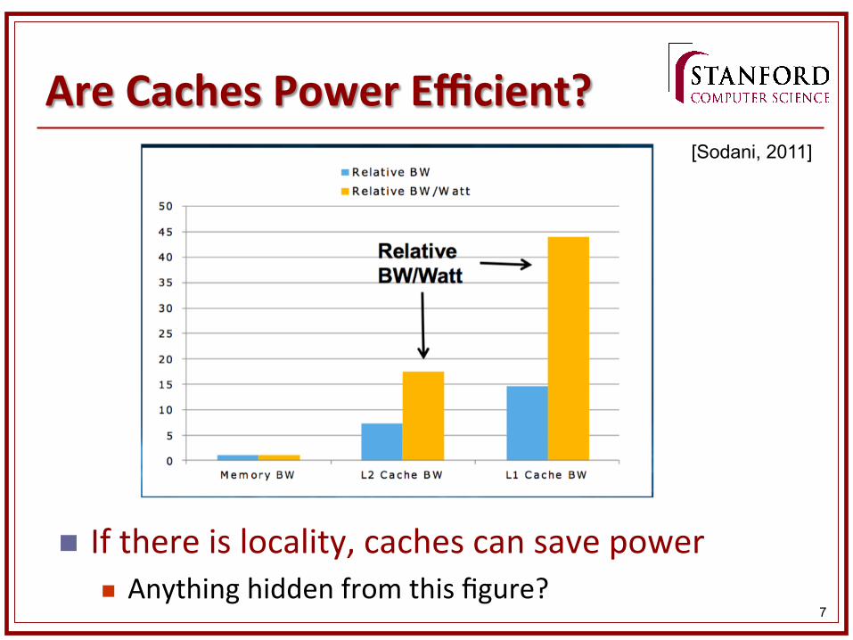
Are Caches Power Efficient?
n If there is locality, caches can save power n Anything hidden from this figure?
[Sodani, 2011]
8
Discussion
n How would you improve the power consump&on of an LLC?
9
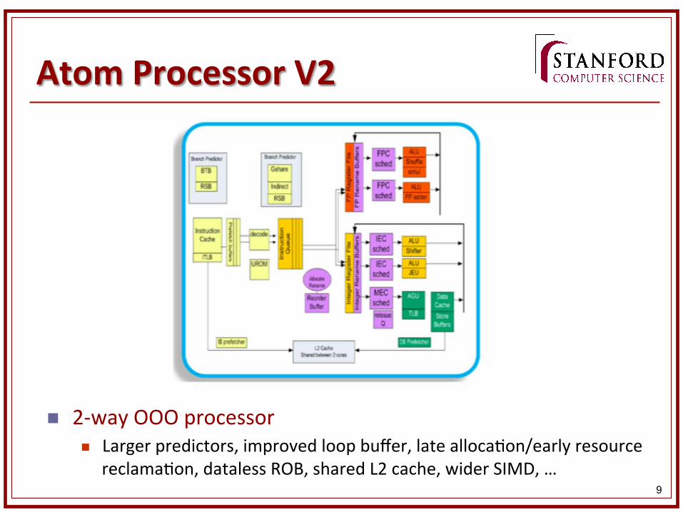
Atom Processor V2
n 2-‐way OOO processor n Larger predictors, improved loop buffer, late alloca&on/early resource
reclama&on, dataless ROB, shared L2 cache, wider SIMD, …
10
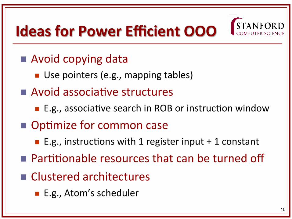
Ideas for Power Efficient OOO
n Avoid copying data n Use pointers (e.g., mapping tables)
n Avoid associa&ve structures n E.g., associa&ve search in ROB or instruc&on window
n Op&mize for common case n E.g., instruc&ons with 1 register input + 1 constant
n Par&&onable resources that can be turned off n Clustered architectures
n E.g., Atom’s scheduler
11
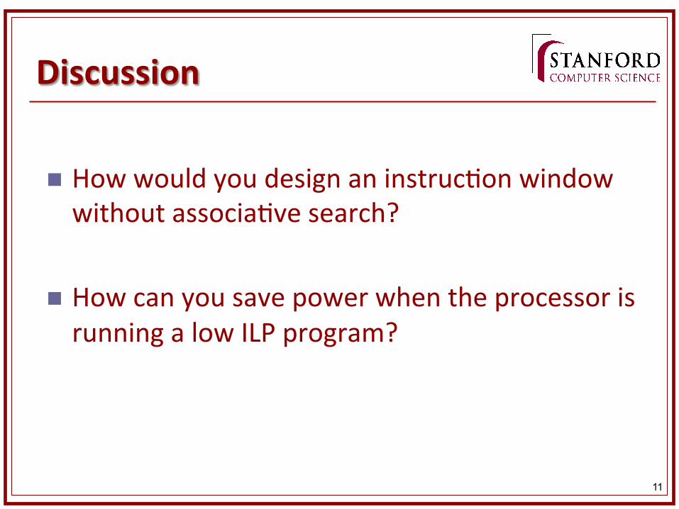
Discussion
n How would you design an instruc&on window without associa&ve search?
n How can you save power when the processor is running a low ILP program?
12
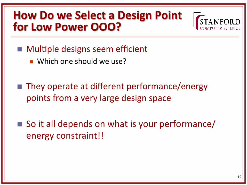
How Do we Select a Design Point for Low Power OOO?
n Mul&ple designs seem efficient n Which one should we use?
n They operate at different performance/energy points from a very large design space
n So it all depends on what is your performance/energy constraint!!
13
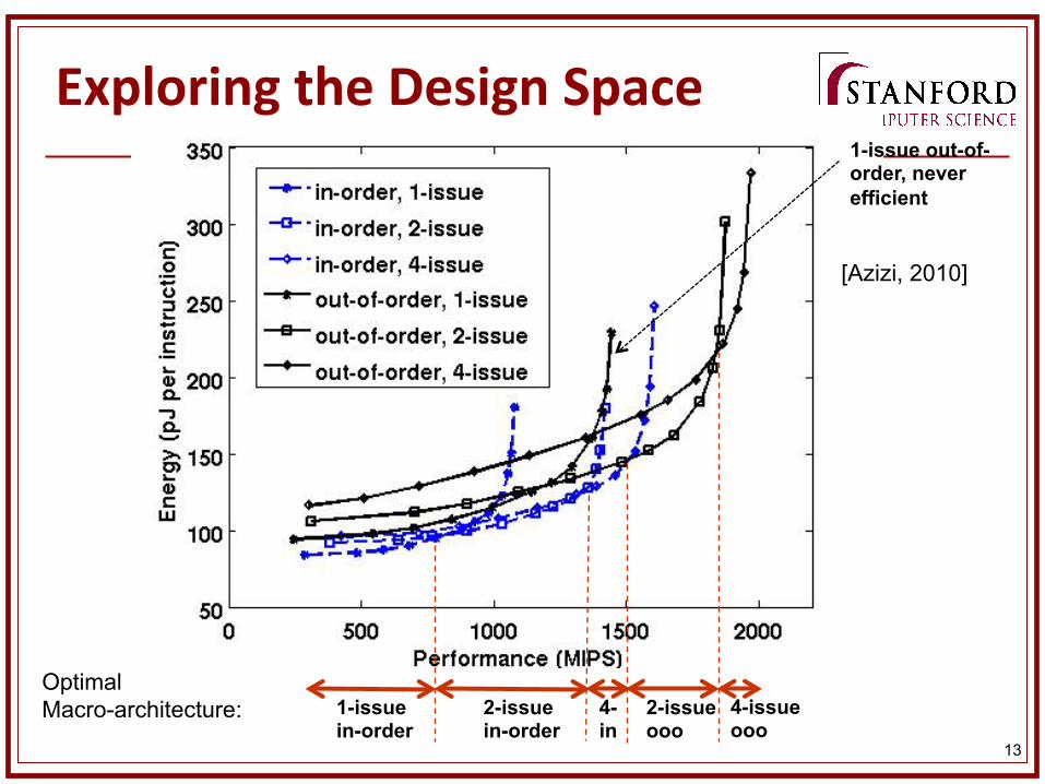
Exploring the Design Space
1-issue in-order
2-issue in-order
2-issue ooo
4-issue ooo
Optimal Macro-architecture: 4-
in
1-issue out-of-order, never efficient
[Azizi, 2010]
14
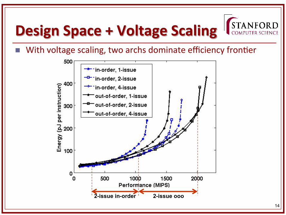
Design Space + Voltage Scaling
2-issue ooo 2-issue in-order
n With voltage scaling, two archs dominate efficiency fron&er
15
What Changes with MulK-‐core?
n With mul&-‐cores per chip and parallel programs, can we just use the simplest core and rely on parallelism?
n The problems n Sequen&al workloads (need a be1er core) n Amdahl’s law for parallel workloads
n We s&ll need a capable core for ILP n And it should be energy efficient
16
Why Do We SKll Care About ILP n Mark Hill’s argument based on Amdahl’s Law
n www.cs.wisc.edu/mul&facet/papers/hpca08_keynote_amdahl.ppt
n Assume a resource limited mul&-‐core n N basic core equivalent (BCEs) due to area or power constraints n A 1 BCE core leads to performance of 1 n A R BCE core leads to performance of perf(R)
n Assuming perf(R) = sqrt(R) in following drawings
n How should be design the mul&-‐core? n Select type and number of cores n Assump&on: caches, interconnect,etc are rather constant n Assump&on: no applica&on scaling (or equal scaling for seq/par por&ons)
17
The 3 CMP Design Approaches
Large Cores (R BCEs/core)
Simple Cores (1 BCE/core)
Number Performance Number Performance
Symmetric CMP N/R Seq: Perf(R) Par: (N/R)*Perf(R)
-‐ -‐
Asymmetric CMP 1 Seq: Perf(R) Par: Perf(R)
N-‐R Seq: 1 Par: (N-‐R)*1
Dynamic CMP 1 Seq: Perf(R) Par: -‐
N Seq: -‐ Par: N

18
Amdahl’s Law x3 n Symmetric CMP
n Asymmetric CMP
n Dynamic CMP
Speedup = 1
+ 1 - F Perf(R)
F * R
Perf(R)*N
Speedup = 1
+ 1 - F Perf(R)
F
Perf(R) + N - R
Speedup = 1
+ 1 - F Perf(R)
F
N
19
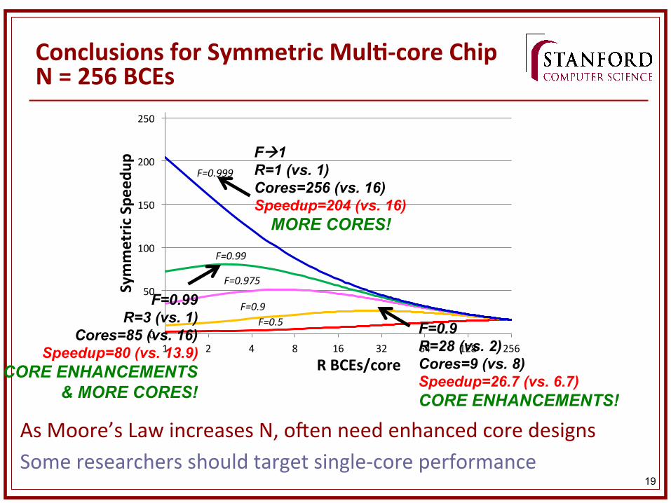
Conclusions for Symmetric MulK-‐core Chip N = 256 BCEs
As Moore’s Law increases N, onen need enhanced core designs Some researchers should target single-‐core performance
0
50
100
150
200
250
1 2 4 8 16 32 64 128 256
Symmetric
Spe
edup
R BCEs/core
F=0.999
F=0.99
F=0.975
F=0.9 F=0.5 F=0.9
R=28 (vs. 2) Cores=9 (vs. 8) Speedup=26.7 (vs. 6.7) CORE ENHANCEMENTS!
Fà1 R=1 (vs. 1) Cores=256 (vs. 16) Speedup=204 (vs. 16) MORE CORES!
F=0.99 R=3 (vs. 1)
Cores=85 (vs. 16) Speedup=80 (vs. 13.9)
CORE ENHANCEMENTS & MORE CORES!
20
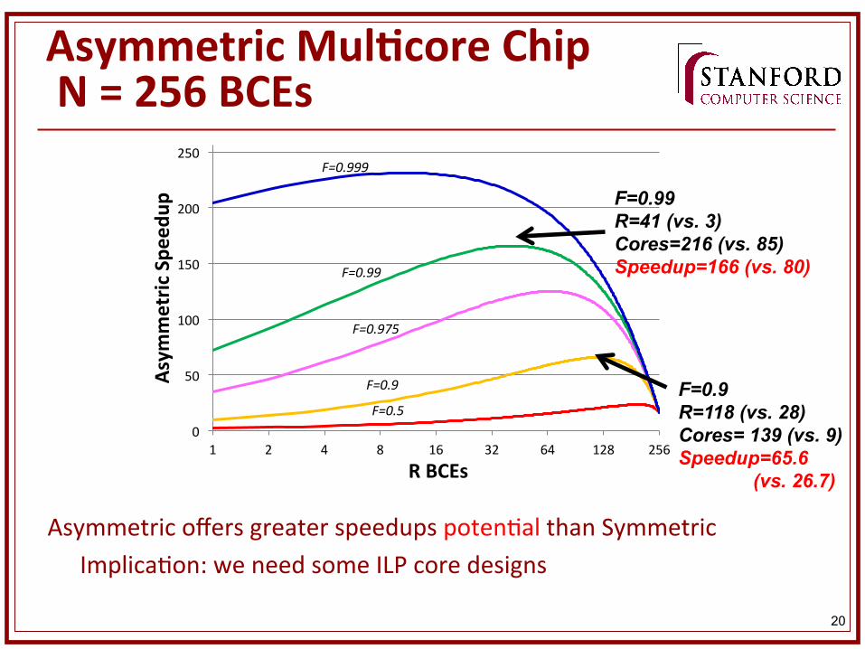
Asymmetric MulKcore Chip N = 256 BCEs
Asymmetric offers greater speedups poten&al than Symmetric Implica&on: we need some ILP core designs
0
50
100
150
200
250
1 2 4 8 16 32 64 128 256
Asym
metric
Spe
edup
R BCEs
F=0.999
F=0.99
F=0.975
F=0.9
F=0.5 F=0.9 R=118 (vs. 28) Cores= 139 (vs. 9) Speedup=65.6 (vs. 26.7)
F=0.99 R=41 (vs. 3) Cores=216 (vs. 85) Speedup=166 (vs. 80)

21
Dynamic MulKcore Chip N = 256 BCEs
Dynamic offers greater speedup poten&al than Asymmetric (but it’s not easy to be jack of all trades) Implica&on: we need some ILP core designs
0
50
100
150
200
250
1 2 4 8 16 32 64 128 256
Dyna
mic Spe
edup
R BCEs
F=0.999
F=0.99
F=0.975
F=0.9
F=0.5
F=0.99 R=256 (vs. 41) Cores=256 (vs. 216) Speedup=223 (vs. 166)
Note: #Cores always N=256
22
Discussion n How do we reduce energy/power even further ?
n Remember, we are missing a factor of 2x per genera&on n Difficult to achieve it by tweaking OOO parameters
n Methodology?
n Known alterna&ves to general-‐purpose processors? n What are their pros and cons?
23
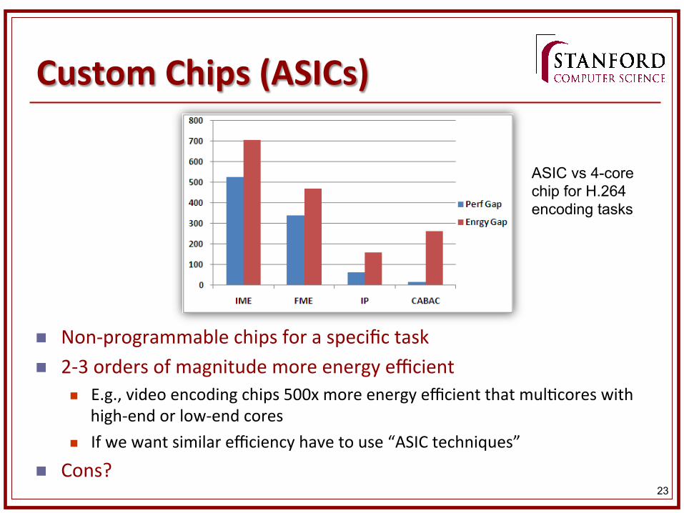
Custom Chips (ASICs)
n Non-‐programmable chips for a specific task n 2-‐3 orders of magnitude more energy efficient
n E.g., video encoding chips 500x more energy efficient that mul&cores with high-‐end or low-‐end cores
n If we want similar efficiency have to use “ASIC techniques”
n Cons?
ASIC vs 4-core chip for H.264 encoding tasks
24
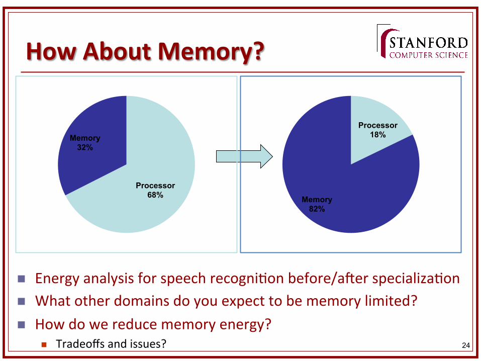
How About Memory?
n Energy analysis for speech recogni&on before/aner specializa&on n What other domains do you expect to be memory limited? n How do we reduce memory energy?
n Tradeoffs and issues?
Processor 18%
Memory 82%
Processor 68%
Memory 32%

25
New Memory Technologies
26
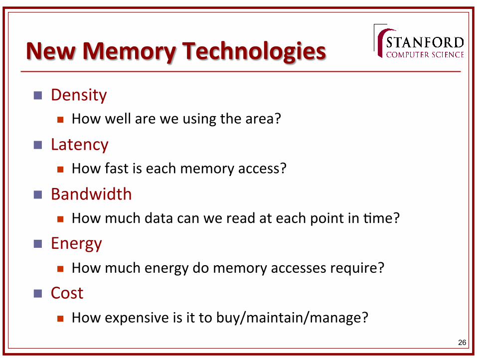
New Memory Technologies n Density
n How well are we using the area?
n Latency n How fast is each memory access?
n Bandwidth n How much data can we read at each point in &me?
n Energy n How much energy do memory accesses require?
n Cost n How expensive is it to buy/maintain/manage?
27
Why Not Just DRAM? n Advantages:
n Prevalent – almost every system uses it n Fast(er) than NVM (~60ns reads) n High write bw (1000MB/s) n Structural simplicity (1 transistor + capacitor per bit) n Moderately dense n Endurance (infinite)
n Disadvantages: n Expensive n Not that fast (latency is not improving a lot) n Reten&on (needs refresh – every ~64ms per row) n Vola&le (loses data on power-‐down) n High energy overhead
28
Why Not Just DRAM? n Capacity doubles every two years (Moore’s Law) BUT latency changes li1le n Can improve latency (and power) by building smaller blocks à hurts density & cost
n Can improve latency (and power) by being clever about access scheduling & mapping data to rows à increases hit rate, but also increases complexity
n Will soon hit a density wall à need alterna&ve technologies
29
AlternaKve Technologies
n Flash n PCM n STT-‐RAM n FRAM (or FeRAM) – Ferroelectric RAM n MRAM (Magneto Resis&ve RAM) n Memristors n …
30
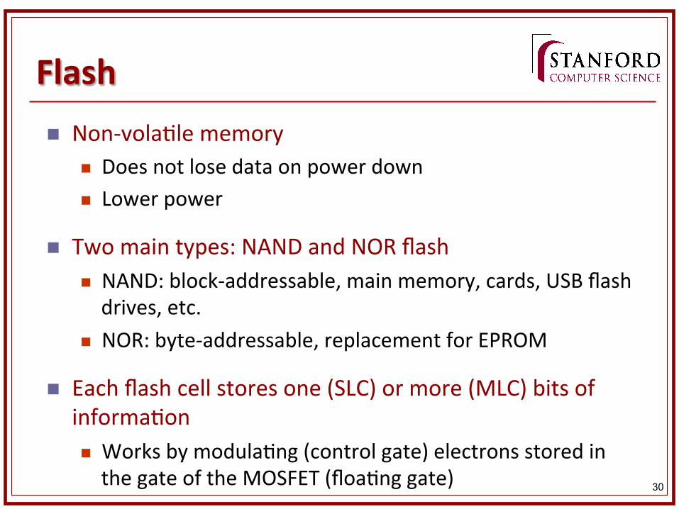
Flash n Non-‐vola&le memory
n Does not lose data on power down n Lower power
n Two main types: NAND and NOR flash n NAND: block-‐addressable, main memory, cards, USB flash drives, etc.
n NOR: byte-‐addressable, replacement for EPROM
n Each flash cell stores one (SLC) or more (MLC) bits of informa&on n Works by modula&ng (control gate) electrons stored in the gate of the MOSFET (floa&ng gate)
31
Flash
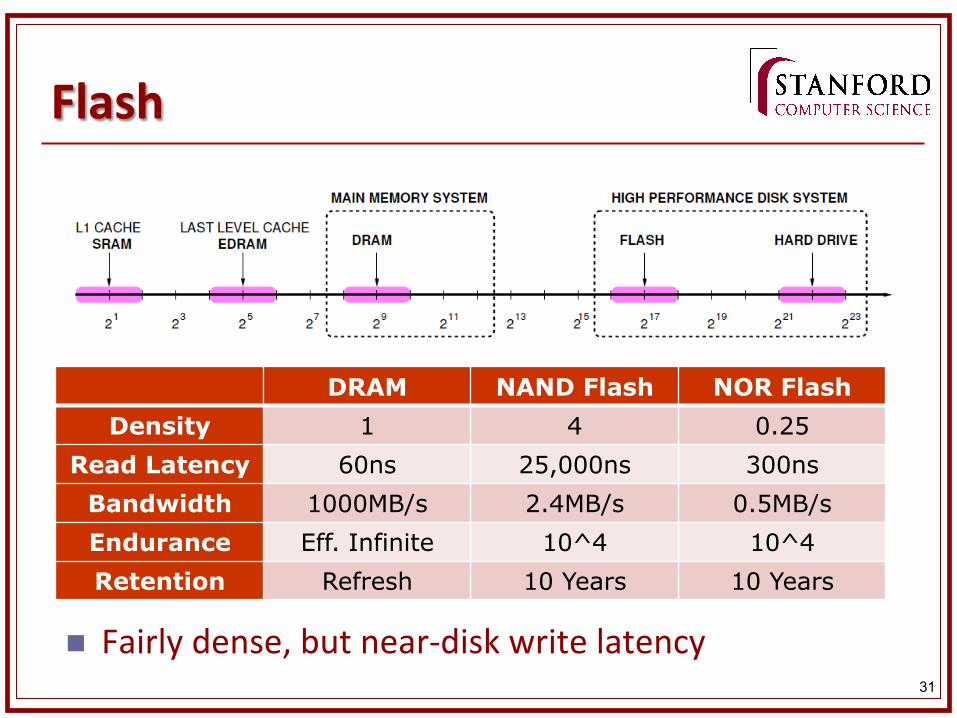
n Fairly dense, but near-‐disk write latency
DRAM NAND Flash NOR Flash Density 1 4 0.25
Read Latency 60ns 25,000ns 300ns Bandwidth 1000MB/s 2.4MB/s 0.5MB/s Endurance Eff. Infinite 10^4 10^4 Retention Refresh 10 Years 10 Years
32
Phase Change Memory (PCM)
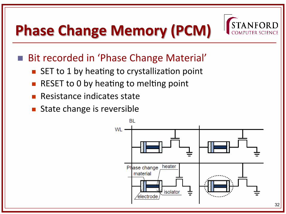
n Bit recorded in ‘Phase Change Material’ n SET to 1 by hea&ng to crystalliza&on point n RESET to 0 by hea&ng to mel&ng point n Resistance indicates state n State change is reversible
33
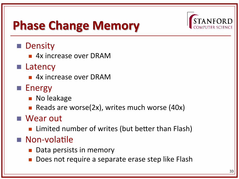
Phase Change Memory n Density
n 4x increase over DRAM n Latency
n 4x increase over DRAM n Energy
n No leakage n Reads are worse(2x), writes much worse (40x)
n Wear out n Limited number of writes (but be1er than Flash)
n Non-‐vola&le n Data persists in memory n Does not require a separate erase step like Flash
34
Phase Change Memory
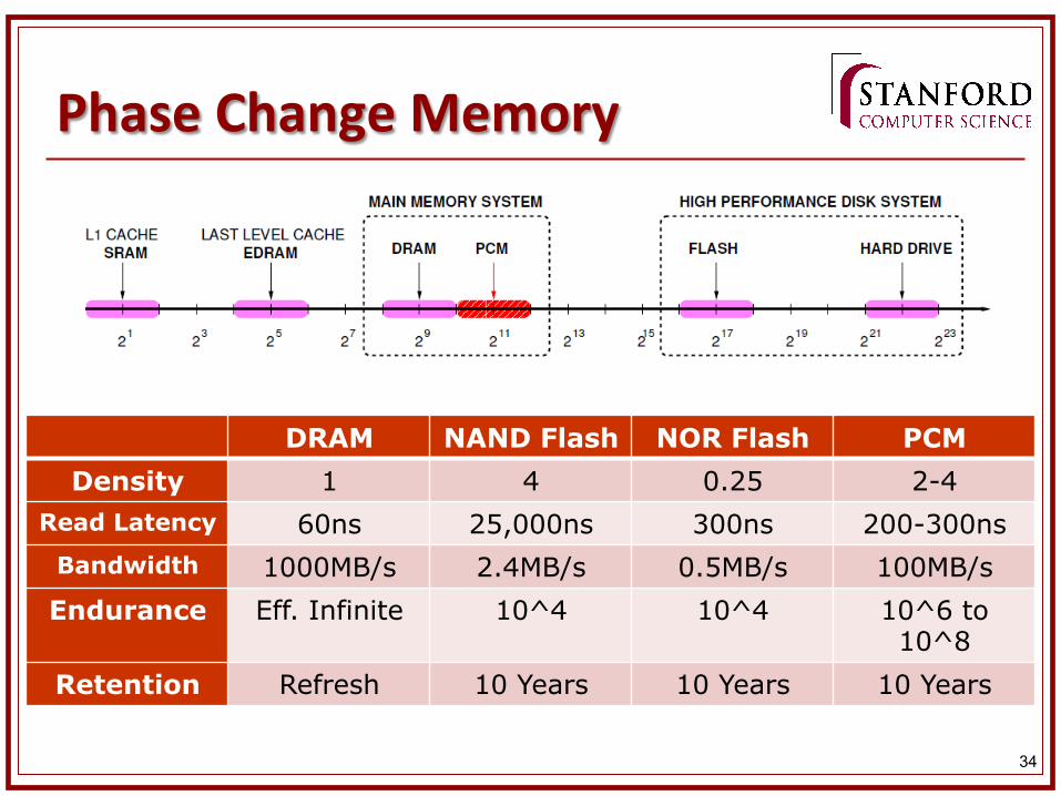
DRAM NAND Flash NOR Flash PCM Density 1 4 0.25 2-4
Read Latency 60ns 25,000ns 300ns 200-300ns Bandwidth 1000MB/s 2.4MB/s 0.5MB/s 100MB/s Endurance Eff. Infinite 10^4 10^4 10^6 to
10^8 Retention Refresh 10 Years 10 Years 10 Years
35
Phase Change Memory
n Main problems (compared to DRAM)?

36
SoluKons to wearing & energy
n Two main techniques?
37
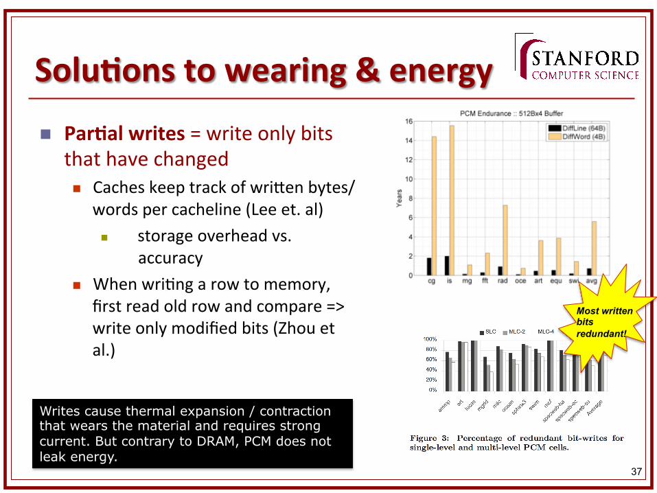
SoluKons to wearing & energy
n ParKal writes = write only bits that have changed n Caches keep track of wri1en bytes/
words per cacheline (Lee et. al) n storage overhead vs.
accuracy n When wri&ng a row to memory,
first read old row and compare => write only modified bits (Zhou et al.)
Writes cause thermal expansion / contraction that wears the material and requires strong current. But contrary to DRAM, PCM does not leak energy.
Most written bits redundant!
38
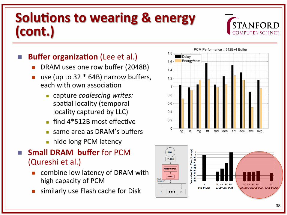
SoluKons to wearing & energy (cont.)
n Buffer organizaKon (Lee et al.) n DRAM uses one row buffer (2048B) n use (up to 32 * 64B) narrow buffers,
each with own associa&on n capture coalescing writes: spa&al locality (temporal locality captured by LLC)
n find 4*512B most effec&ve n same area as DRAM’s buffers n hide long PCM latency
n Small DRAM buffer for PCM (Qureshi et al.) n combine low latency of DRAM with
high capacity of PCM n similarly use Flash cache for Disk
39
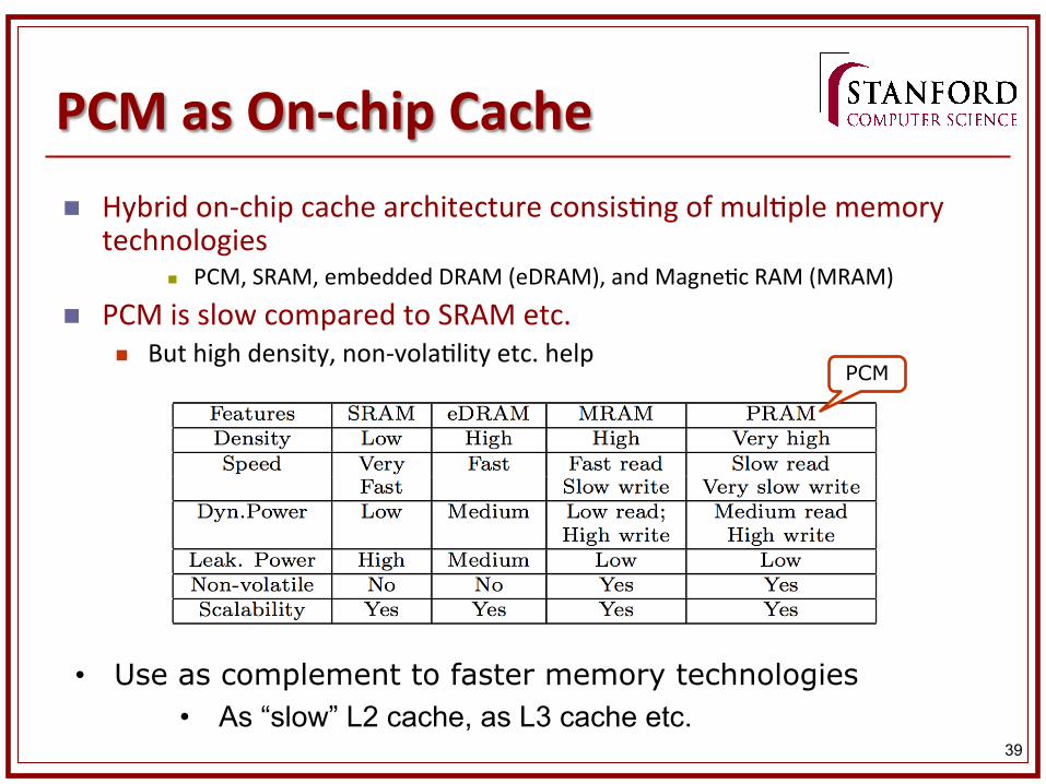
PCM as On-‐chip Cache n Hybrid on-‐chip cache architecture consis&ng of mul&ple memory
technologies n PCM, SRAM, embedded DRAM (eDRAM), and Magne&c RAM (MRAM)
n PCM is slow compared to SRAM etc. n But high density, non-‐vola&lity etc. help
• Use as complement to faster memory technologies • As “slow” L2 cache, as L3 cache etc.
PCM
40
STT-‐RAM n STT-‐RAM: Spin-‐transfer torque RAM
n Non-‐vola&le technology n Opera&on: change the orienta&on of a magne&c layer in a magne&c tunnel junc&on (or spin valve)
n Essen&ally creates spin-‐polarized current by passing an electric current through a think magne&c material (fixed layer) à direct current to second thin magne&c material (free layer) to change its orienta&on
n Needs lower current than tradi&onal MRAM à higher densi&es
41
STT-‐RAM n Advantages:
n Higher density than RAM (lower current needed) n Non-‐vola&le (can replace SRAM for processor caches) n Low leakage à low sta&c power consump&on n High endurance n Good performance (reads)
n Disadvantages: n High dynamic energy n Slow write latencies n Lower endurance compared to RAM
42
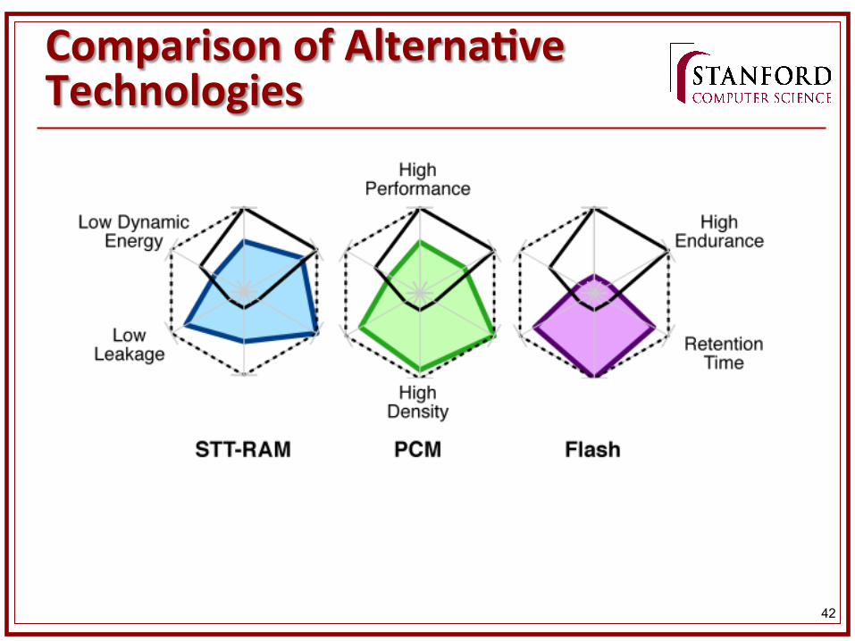
Comparison of AlternaKve Technologies
43
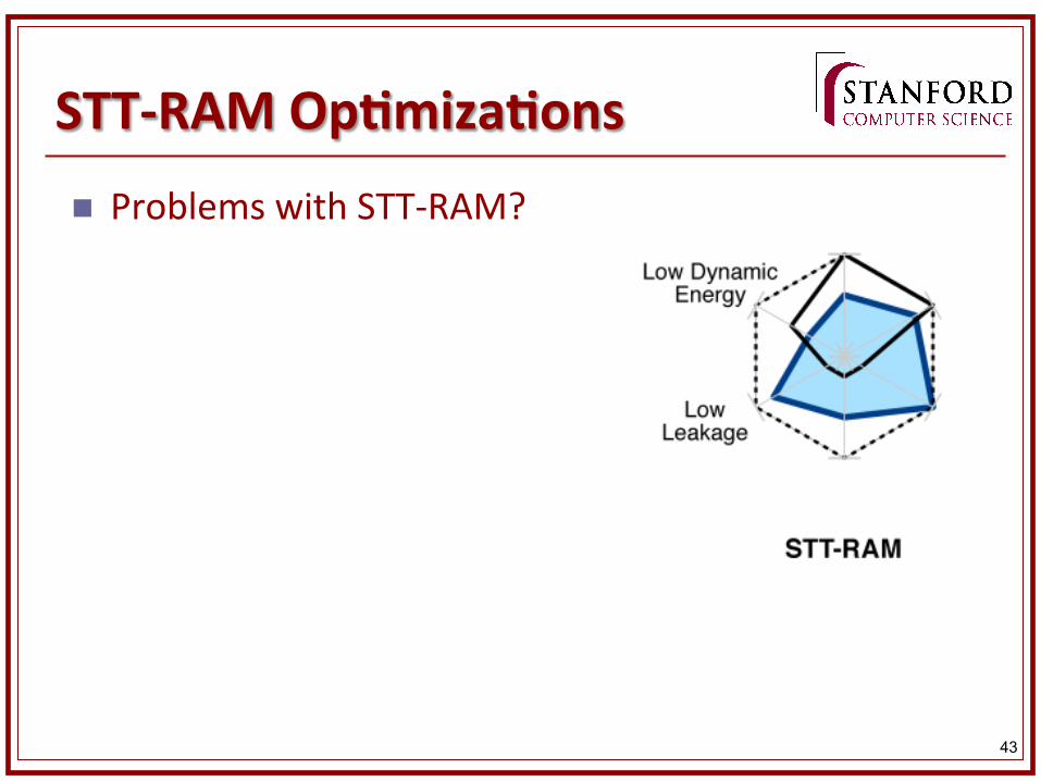
STT-‐RAM OpKmizaKons n Problems with STT-‐RAM?
44
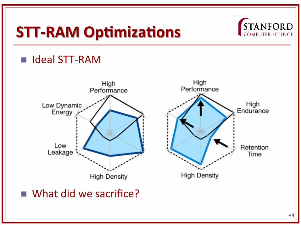
STT-‐RAM OpKmizaKons n Ideal STT-‐RAM
n What did we sacrifice?
45
STT-‐RAM OpKmizaKons n Reduced reten&on &me STT-‐RAM
n Reduce the area of the free layer of the magne&c tunnel junc&on (MTJ) (storage element for STT-‐RAM cell) à reduce energy needed to write to the cell
n Is sacrificing reten&on a good idea? n How much should we sacrifice?
n How can they scale from small structures to large structures?
n Do we need any new opera&ons?
46
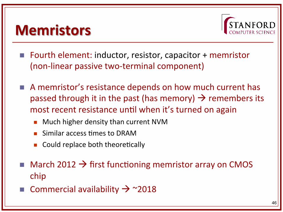
Memristors n Fourth element: inductor, resistor, capacitor + memristor
(non-‐linear passive two-‐terminal component)
n A memristor’s resistance depends on how much current has passed through it in the past (has memory) à remembers its most recent resistance un&l when it’s turned on again n Much higher density than current NVM n Similar access &mes to DRAM n Could replace both theore&cally
n March 2012 à first func&oning memristor array on CMOS chip
n Commercial availability à ~2018
47
AlternaKve Memory Systems n Not necessarily change the memory technology (can s&ll use DRAM), but change the way the memory system is designed and managed n Reduce overfetch à reduce power by being clever about how much data is read (read fewer chips, or only parts of a row)
n Build hybrid/heterogeneous memory systems n Near-‐Data Processing (NDP) n 3D stacked RAM n …
48
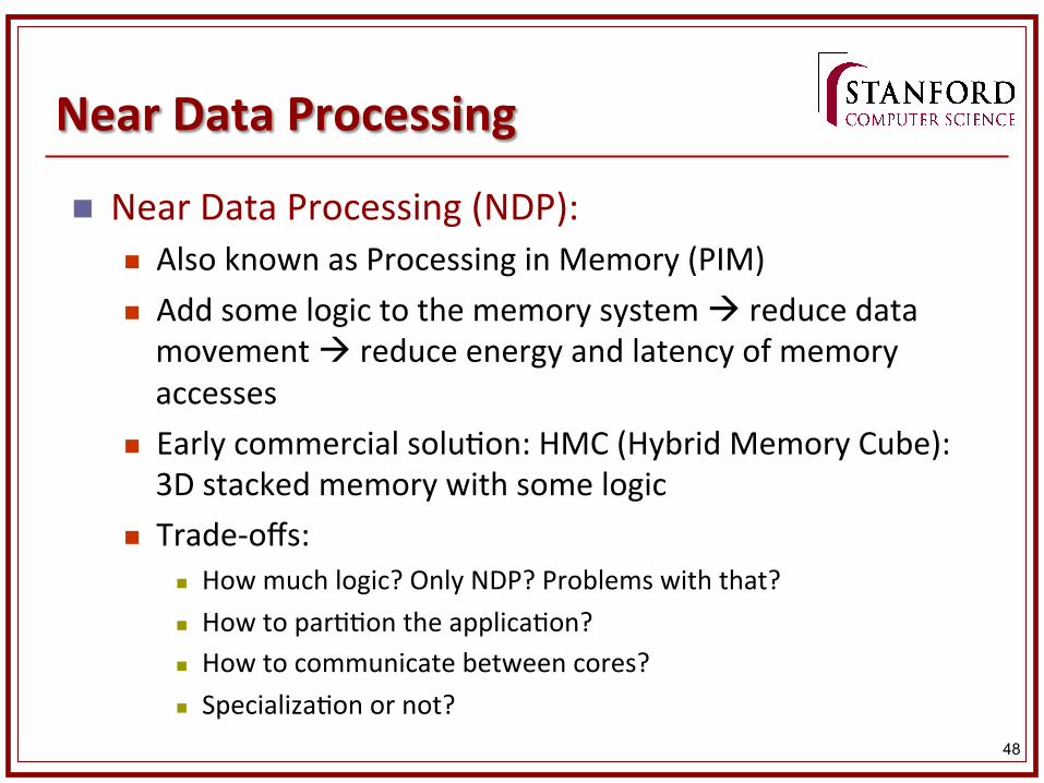
Near Data Processing
n Near Data Processing (NDP): n Also known as Processing in Memory (PIM) n Add some logic to the memory system à reduce data movement à reduce energy and latency of memory accesses
n Early commercial solu&on: HMC (Hybrid Memory Cube): 3D stacked memory with some logic
n Trade-‐offs: n How much logic? Only NDP? Problems with that? n How to par&&on the applica&on? n How to communicate between cores? n Specializa&on or not?
49
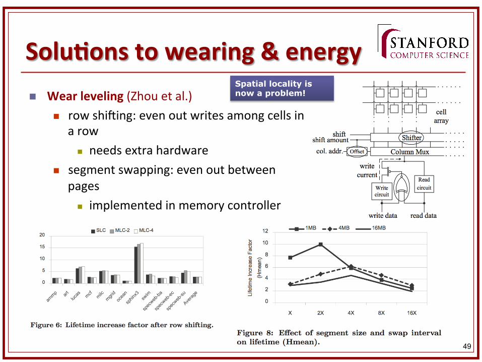
SoluKons to wearing & energy n Wear leveling (Zhou et al.)
n row shining: even out writes among cells in a row
n needs extra hardware n segment swapping: even out between
pages n implemented in memory controller
Spatial locality is now a problem!


![Data Tiering in Heterogeneous Memory Systems · To address this challenge, industry is exploring new non-volatile memory technologies (or NVM) [6, 30, 46]. These memory technologies](https://img.pdfslide.us/doc/110x75/60b13ba9ca7fbc30cf6254ee/data-tiering-in-heterogeneous-memory-systems-to-address-this-challenge-industry.jpg)