Embed Size (px)
Citation preview
1
Low Power System-On-Chip DesignChapter 13:Chapter 13:
Retention Register Design
Ismo Hänninen
Institute of Digital and Computer Systems / TKT-9636Department of Computer Systems / TKT-9626Department of Computer Systems / TKT-9626 Ch13: Retention Register Design 1/8/2009
2
Chapter 13: Retention Register Designp g g
Overview
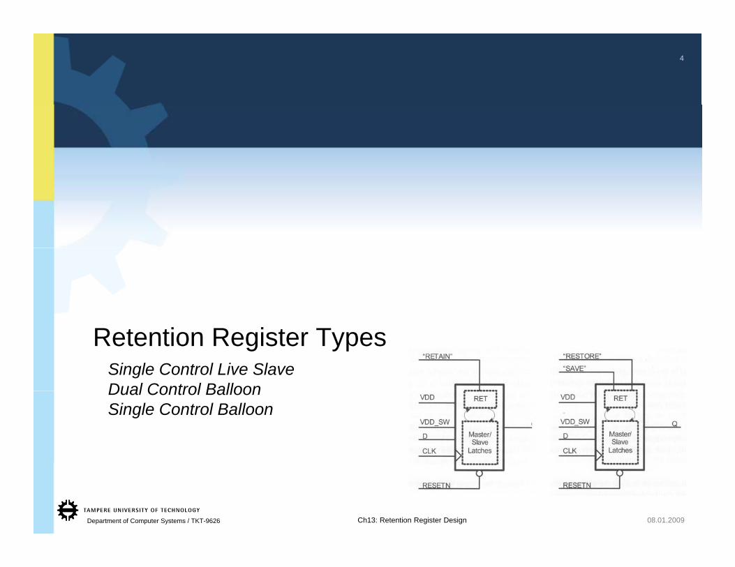
Retention Register TypesSingle Control Live SlaveDual Control BalloonSingle Control Balloon
Retention Register Relative LayoutsRetention Register Relative Layouts
Memory Retention MethodsReduced VDD RetentionReduced VDD RetentionSource-Diode BiasingSource Biasing
Memory Retention Latency Reduction
Institute of Digital and Computer Systems / TKT-9636Department of Computer Systems / TKT-9626 Ch13: Retention Register Design 1/8/2009
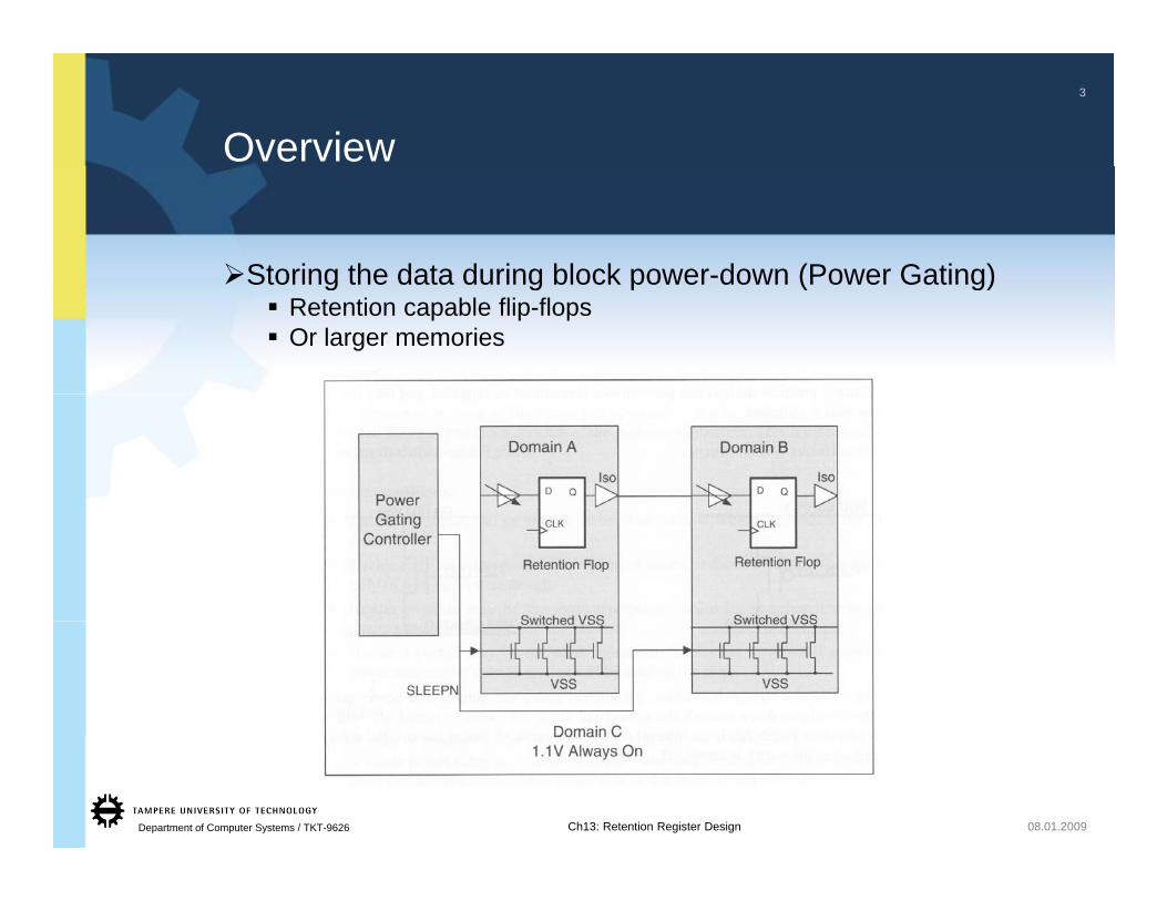
Overview3
Storing the data during block power-down (Power Gating)Storing the data during block power down (Power Gating)Retention capable flip-flopsOr larger memories
Institute of Digital and Computer Systems / TKT-9636Department of Computer Systems / TKT-9626 Ch13: Retention Register Design 08.01.2009
4
Single Control Live SlaveDual Control Balloon
Retention Register Types
Dual Control BalloonSingle Control Balloon
Institute of Digital and Computer Systems / TKT-9636Department of Computer Systems / TKT-9626 Ch13: Retention Register Design 08.01.2009
Single Control Live Slave5
g
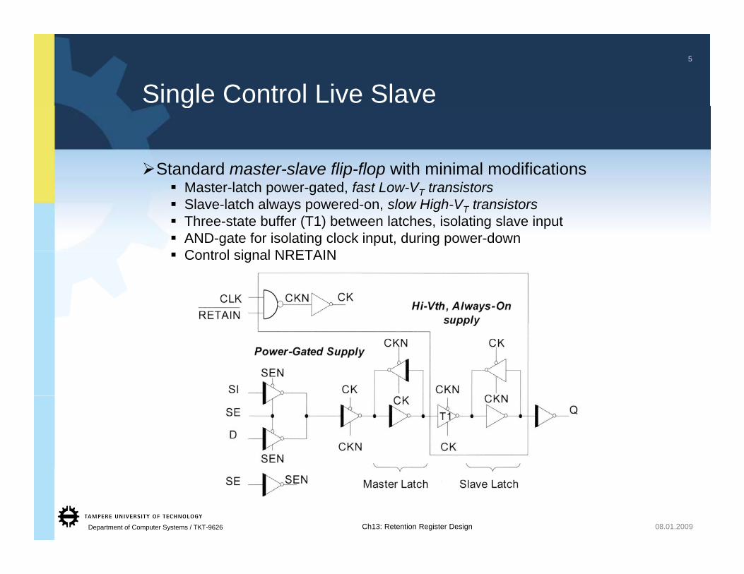
Standard master-slave flip-flop with minimal modificationsMaster-latch power-gated, fast Low-VT transistorsSlave-latch always powered-on, slow High-VT transistorsThree-state buffer (T1) between latches, isolating slave inputAND-gate for isolating clock input, during power-downC t l i l NRETAINControl signal NRETAIN
Institute of Digital and Computer Systems / TKT-9636Department of Computer Systems / TKT-9626 Ch13: Retention Register Design 08.01.2009
…Single Control Live Slave6
g
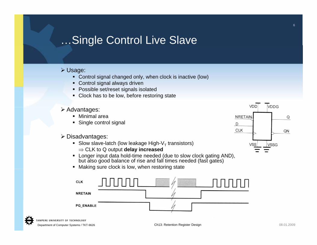
Usage:Control signal changed only when clock is inactive (low)Control signal changed only, when clock is inactive (low)Control signal always drivenPossible set/reset signals isolatedClock has to be low, before restoring state
Advantages:Minimal areaSingle control signal
Disadvantages:Disadvantages:Slow slave-latch (low leakage High-VT transistors)⇒ CLK to Q output delay increasedLonger input data hold-time needed (due to slow clock gating AND), but also good balance of rise and fall times needed (fast gates)Making sure clock is low, when restoring stateg , g
Institute of Digital and Computer Systems / TKT-9636Department of Computer Systems / TKT-9626 Ch13: Retention Register Design 08.01.2009
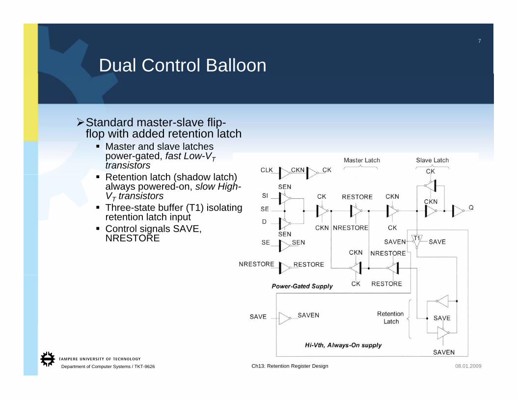
Dual Control Balloon7
Standard master-slave flip-Standard master slave flipflop with added retention latch
Master and slave latches power-gated, fast Low-VTtransistorsR t ti l t h ( h d l t h)Retention latch (shadow latch) always powered-on, slow High-VT transistorsThree-state buffer (T1) isolating retention latch inputControl signals SAVE, NRESTORE
Institute of Digital and Computer Systems / TKT-9636Department of Computer Systems / TKT-9626 Ch13: Retention Register Design 08.01.2009
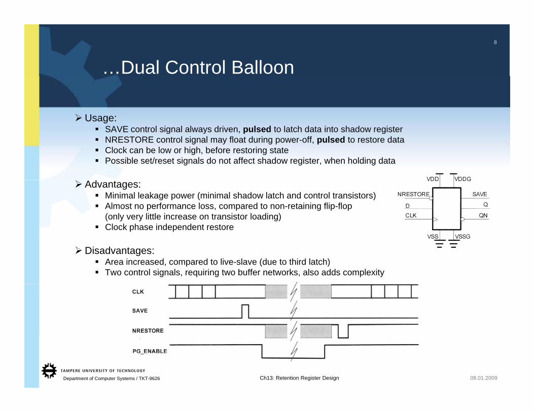
…Dual Control Balloon8
Usage:SAVE control signal always driven pulsed to latch data into shadow registerSAVE control signal always driven, pulsed to latch data into shadow registerNRESTORE control signal may float during power-off, pulsed to restore dataClock can be low or high, before restoring statePossible set/reset signals do not affect shadow register, when holding data
Advantages:Minimal leakage power (minimal shadow latch and control transistors)Almost no performance loss, compared to non-retaining flip-flop(only very little increase on transistor loading)Clock phase independent restore
Disadvantages:Area increased, compared to live-slave (due to third latch)Two control signals, requiring two buffer networks, also adds complexity
Institute of Digital and Computer Systems / TKT-9636Department of Computer Systems / TKT-9626 Ch13: Retention Register Design 08.01.2009
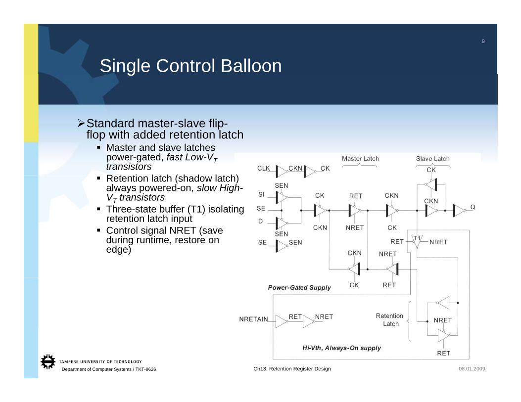
Single Control Balloon9
g
Standard master-slave flip-Standard master slave flipflop with added retention latch
Master and slave latches power-gated, fast Low-VTtransistorsR t ti l t h ( h d l t h)Retention latch (shadow latch) always powered-on, slow High-VT transistorsThree-state buffer (T1) isolating retention latch inputControl signal NRET (save during runtime, restore on edge)
Institute of Digital and Computer Systems / TKT-9636Department of Computer Systems / TKT-9626 Ch13: Retention Register Design 08.01.2009
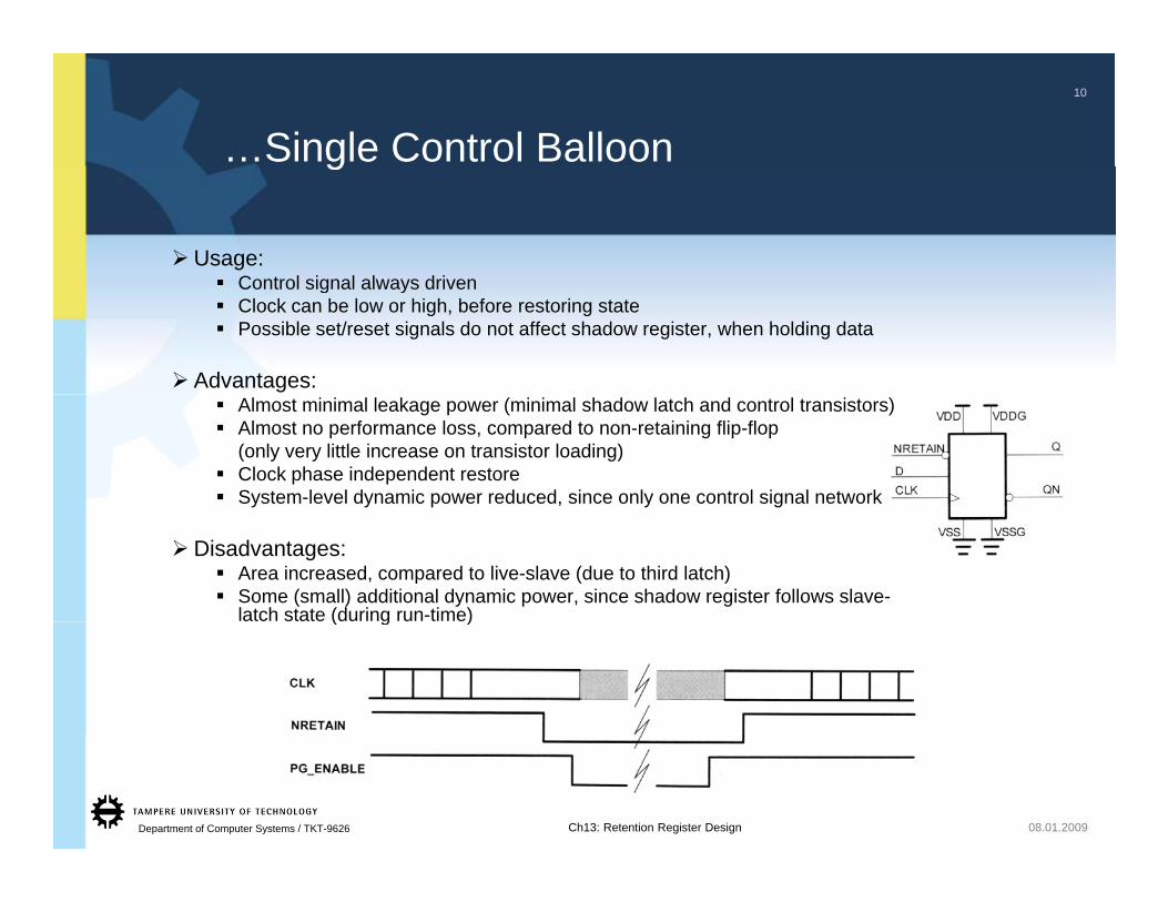
…Single Control Balloon10
g
Usage:Control signal always drivenControl signal always drivenClock can be low or high, before restoring statePossible set/reset signals do not affect shadow register, when holding data
Advantages:Almost minimal leakage power (minimal shadow latch and control transistors)Almost no performance loss, compared to non-retaining flip-flop(only very little increase on transistor loading)Clock phase independent restoreSystem-level dynamic power reduced, since only one control signal network
Disadvantages:Area increased, compared to live-slave (due to third latch)Some (small) additional dynamic power, since shadow register follows slave-latch state (during run-time)( g )
Institute of Digital and Computer Systems / TKT-9636Department of Computer Systems / TKT-9626 Ch13: Retention Register Design 08.01.2009
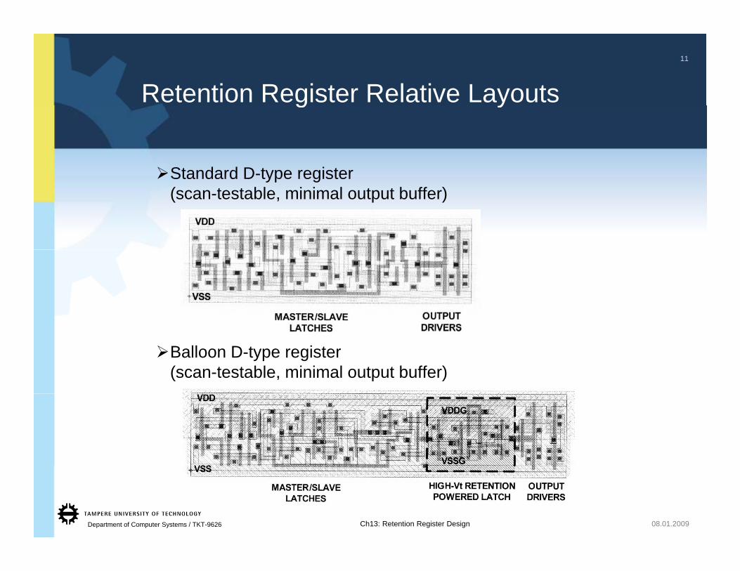
Retention Register Relative Layouts11
g y
Standard D-type registerStandard D type register(scan-testable, minimal output buffer)
Balloon D-type register(scan-testable, minimal output buffer)
Institute of Digital and Computer Systems / TKT-9636Department of Computer Systems / TKT-9626 Ch13: Retention Register Design 08.01.2009
12
Reduced VDD RetentionSource-Diode Biasing
Memory Retention Methods
Source-Diode BiasingSource Biasing
Institute of Digital and Computer Systems / TKT-9636Department of Computer Systems / TKT-9626 Ch13: Retention Register Design 08.01.2009
Memory Retention Methods13
y
Often, FIFOs’, caches, and other memories are allowed to reset after power-down (losing contents)
For minimum wake-up latency, also memory contents have to be retained
Large memories are too expensive to implement by using retention register approach (replacing standard, optimized memory cells)Needs a solution to reduce the basic cell leakage (without corrupting memory contents)
Three basic approaches for SRAM
Institute of Digital and Computer Systems / TKT-9636Department of Computer Systems / TKT-9626 Ch13: Retention Register Design 08.01.2009
Reduced VDD Retention14
Memory is given own power supply, with two modes (VDD):Normal supply voltageReduced (0.5-0.6 V) sleeping voltage
Reduced voltage saves leakage powerMemory contents stay uncorrupted, but cannot be accessed
Simple implementationNo memory circuit change neededA switchable, dedicated power supply added
Institute of Digital and Computer Systems / TKT-9636Department of Computer Systems / TKT-9626 Ch13: Retention Register Design 08.01.2009
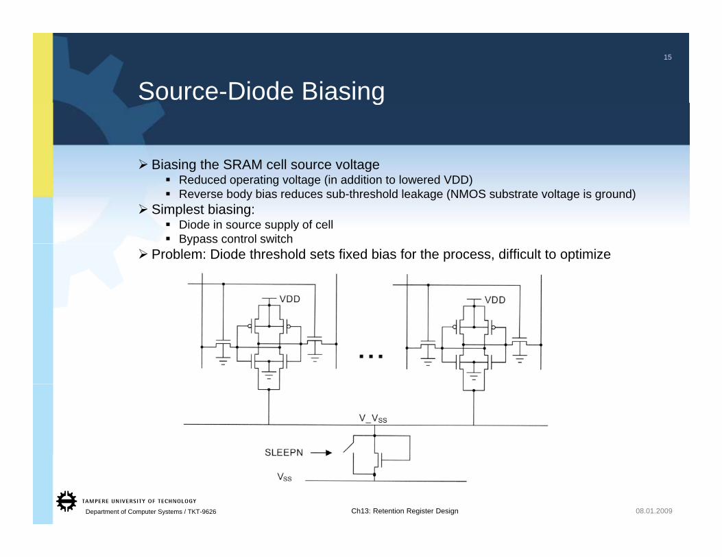
Source-Diode Biasing15
g
Biasing the SRAM cell source voltageReduced operating voltage (in addition to lowered VDD)Reverse body bias reduces sub-threshold leakage (NMOS substrate voltage is ground)
Simplest biasing:Diode in source supply of cellBypass control switchyp
Problem: Diode threshold sets fixed bias for the process, difficult to optimize
Institute of Digital and Computer Systems / TKT-9636Department of Computer Systems / TKT-9626 Ch13: Retention Register Design 08.01.2009
Source Biasing16
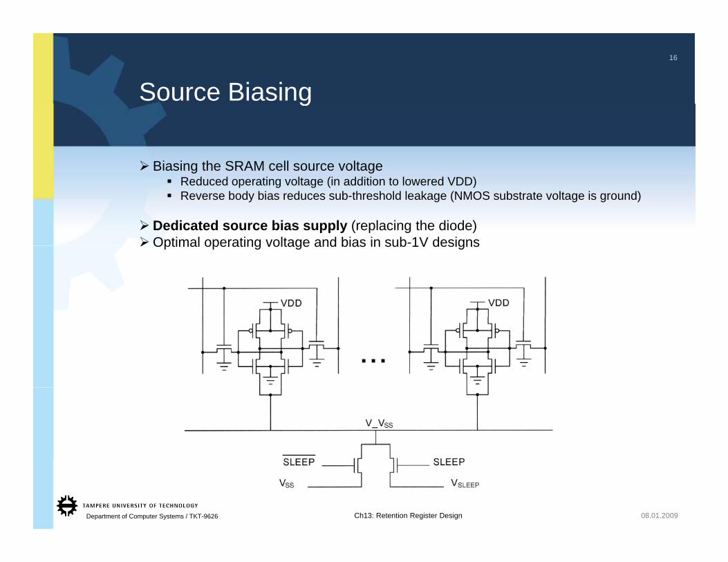
g
Biasing the SRAM cell source voltageReduced operating voltage (in addition to lowered VDD)Reverse body bias reduces sub-threshold leakage (NMOS substrate voltage is ground)
Dedicated source bias supply (replacing the diode)Optimal operating voltage and bias in sub-1V designsOptimal operating voltage and bias in sub 1V designs
Institute of Digital and Computer Systems / TKT-9636Department of Computer Systems / TKT-9626 Ch13: Retention Register Design 08.01.2009
Memory Retention Latency Reduction17
y y
F i hi h t ft d (b t l t i d) ifFor memories, which are not often accessed (but always retained), if short access latency is required
Block-based retention and wakeupM di id d i t b k i di id l t l f l dMemory divided into banks, individual control of sleep modeNormally, bank mode is sleepRead/write access actives only one bank (address decoder)Reduced wakeup latency, since smaller power blocks(smaller virtual VSS network, per bank)( , p )Compromise bank size, speed vs. column overhead(small banks cause area and power overhead in column sense-amps)
Row-based retention and wakeupBiased voltage net for each row, individual control of sleep modeNormally, row mode is sleepRead/write access actives only one rowVery fast, since a row is relatively smallReduced control overhead by using row-grouping
Institute of Digital and Computer Systems / TKT-9636Department of Computer Systems / TKT-9626
Reduced control overhead, by using row-grouping
Ch13: Retention Register Design 08.01.2009
Conclusion18
Retention flip-flops easily replace standard flip-flopsPerformance loss (live slave)Or area penalty (balloon)
For retained memories, the only practical way to save energy during sleep is reduced operating voltage
VDD and VSS moved near each otherSleep/wakeup latency reduction with block/row grouping
Institute of Digital and Computer Systems / TKT-9636Department of Computer Systems / TKT-9626 Ch13: Retention Register Design 08.01.2009