Embed Size (px)
Citation preview
1
Low Power System-On-Chip Design Chapter 12 11.11.08Institute of Digital and Computer Systems / TKT-9636
Low Power System-On-Chip-DesignChapter 12: Physical Libraries
Friedemann Wesner
2
Low Power System-On-Chip Design Chapter 12 11.11.08Institute of Digital and Computer Systems / TKT-9636
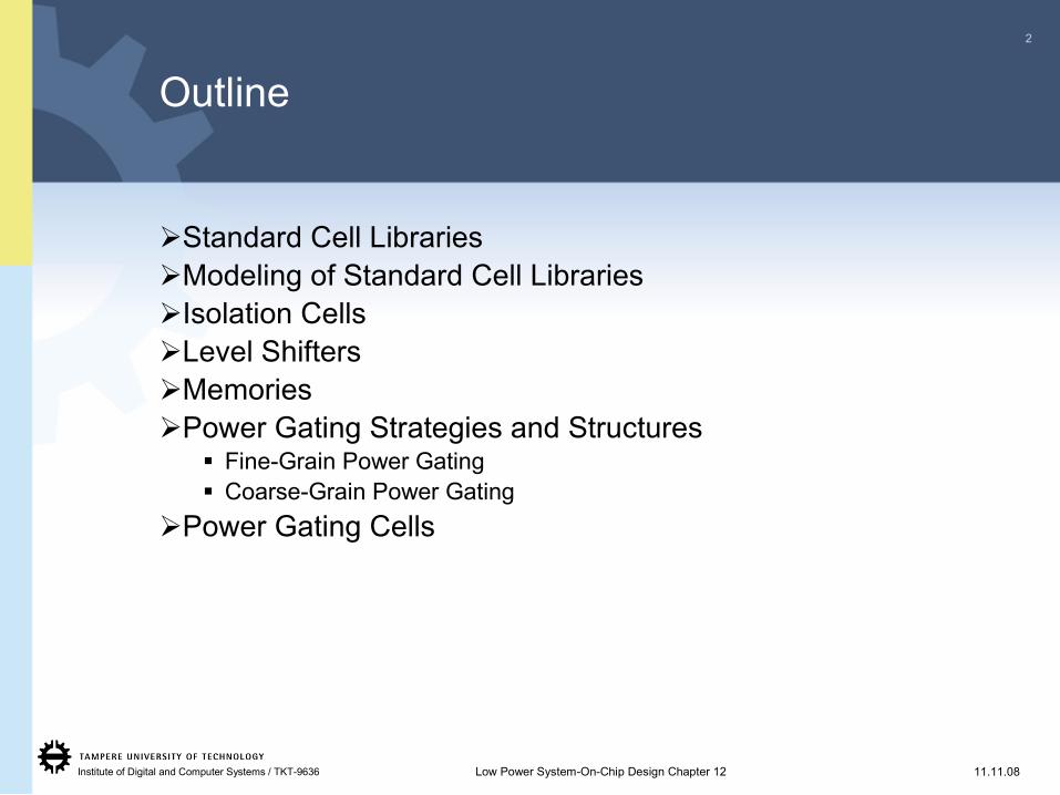
Outline
Standard Cell LibrariesModeling of Standard Cell LibrariesIsolation CellsLevel ShiftersMemoriesPower Gating Strategies and Structures
Fine-Grain Power Gating Coarse-Grain Power Gating
Power Gating Cells
3
Low Power System-On-Chip Design Chapter 12 11.11.08Institute of Digital and Computer Systems / TKT-9636
Standard Cell Libraries
Standard cell libraries may be optimized for Performance Power consumption Required chip area
Choice and mix of used libraries therefore has significant impact on power, timing and area
4
Low Power System-On-Chip Design Chapter 12 11.11.08Institute of Digital and Computer Systems / TKT-9636
...Standard Cell Libraries
Key characteristic of cell libraries is cell height, measured in tracks (1 track = pitch of a Metal one wire)
Tall track height libraries: 11 -12 tracks Optimized for performance, high leakage power
Low track height libraries: 7 – 8 tracks Optimized for area efficiency
Standard track height libraries 9 – 10 tracks Designed to give trade-off between performance and area efficiency Used in majority of designs
5
Low Power System-On-Chip Design Chapter 12 11.11.08Institute of Digital and Computer Systems / TKT-9636
...Standard Cell Libraries
Transistors with different threshold voltage can be used for building a library
High threshold voltage: Lowest leakage power, lower performance
Low threshold voltage: High performance, higher leakage power
Regular threshold voltage: Between high and low threshold voltage libraries
6
Low Power System-On-Chip Design Chapter 12 11.11.08Institute of Digital and Computer Systems / TKT-9636
Modeling of Standard Cell Libraries
Library level provides abstract views of underlying transistor level models
Commercially sensitive internals are hiddenDetailed physical views of cells are switched in for
manufacturing
Required abstract views: Timing models Physical models Functional models Power models Test models
7
Low Power System-On-Chip Design Chapter 12 11.11.08Institute of Digital and Computer Systems / TKT-9636
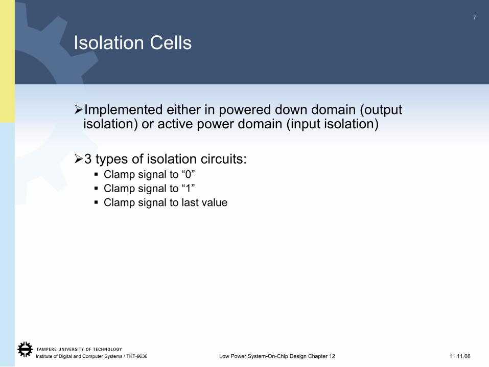
Isolation Cells
Implemented either in powered down domain (output isolation) or active power domain (input isolation)
3 types of isolation circuits: Clamp signal to “0” Clamp signal to “1” Clamp signal to last value
8
Low Power System-On-Chip Design Chapter 12 11.11.08Institute of Digital and Computer Systems / TKT-9636
...Isolation Cells
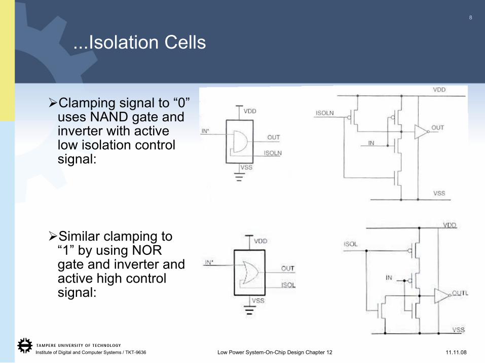
Clamping signal to “0” uses NAND gate and inverter with active low isolation control signal:
Similar clamping to “1” by using NOR gate and inverter and active high control signal:
9
Low Power System-On-Chip Design Chapter 12 11.11.08Institute of Digital and Computer Systems / TKT-9636
...Isolation Cells
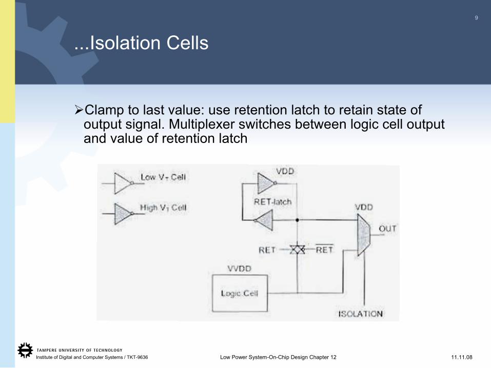
Clamp to last value: use retention latch to retain state of output signal. Multiplexer switches between logic cell output and value of retention latch
10
Low Power System-On-Chip Design Chapter 12 11.11.08Institute of Digital and Computer Systems / TKT-9636
Output vs. Input Isolation
Advantages of output isolation: Only one isolation cell required for output signal going to different
power domains Isolation cells of one domain share a single control signal
Drawback: Custom isolation cells required, since connection to an always-on
power supply must be provided
11
Low Power System-On-Chip Design Chapter 12 11.11.08Institute of Digital and Computer Systems / TKT-9636
Recommendations
Output isolation should be preferred over input isolation
If custom isolation cells are not available, standard cells may be used when placed in an always-on area created for this purpose
Insert isolation cells only when necessary since they introduce delay penalty
12
Low Power System-On-Chip Design Chapter 12 11.11.08Institute of Digital and Computer Systems / TKT-9636
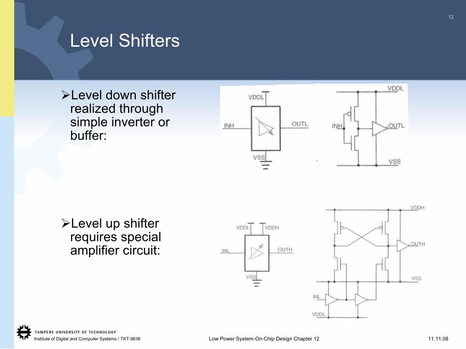
Level Shifters
Level down shifter realized through simple inverter or buffer:
Level up shifter requires special amplifier circuit:
13
Low Power System-On-Chip Design Chapter 12 11.11.08Institute of Digital and Computer Systems / TKT-9636
...Level Shifters
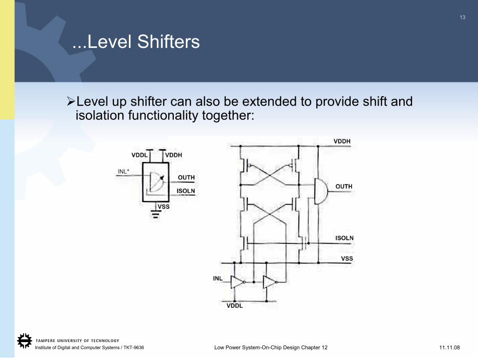
Level up shifter can also be extended to provide shift and isolation functionality together:

14
Low Power System-On-Chip Design Chapter 12 11.11.08Institute of Digital and Computer Systems / TKT-9636
Memories
Usually generated by memory compilers, but for special cases optimized memories may be built as well
Different memory architectures: Single or multi ported RAM RAM array or register file Performance-optimized Area-optimized Power-optimized
Like for logic cells, high (for decreased leakage) or low (increased performance) threshold voltage transistors can be used for implementation
15
Low Power System-On-Chip Design Chapter 12 11.11.08Institute of Digital and Computer Systems / TKT-9636
...Memories
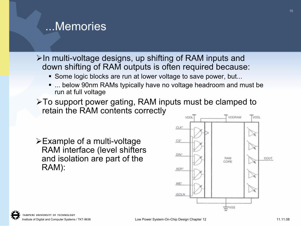
In multi-voltage designs, up shifting of RAM inputs and down shifting of RAM outputs is often required because: Some logic blocks are run at lower voltage to save power, but... ... below 90nm RAMs typically have no voltage headroom and must be
run at full voltageTo support power gating, RAM inputs must be clamped to
retain the RAM contents correctly
Example of a multi-voltage RAM interface (level shifters and isolation are part of the RAM):
16
Low Power System-On-Chip Design Chapter 12 11.11.08Institute of Digital and Computer Systems / TKT-9636
Power Gating Strategies and Structures
2 common approaches for power gating:
Multi-Threshold CMOS (MTCMOS) Use high threshold voltage switches to turn off power (considered in the
following)
Multi-Voltage CMOS (MVCMOS) Use low threshold voltage switches to turn off power Complex to support Rarely used in commercial designs
17
Low Power System-On-Chip Design Chapter 12 11.11.08Institute of Digital and Computer Systems / TKT-9636
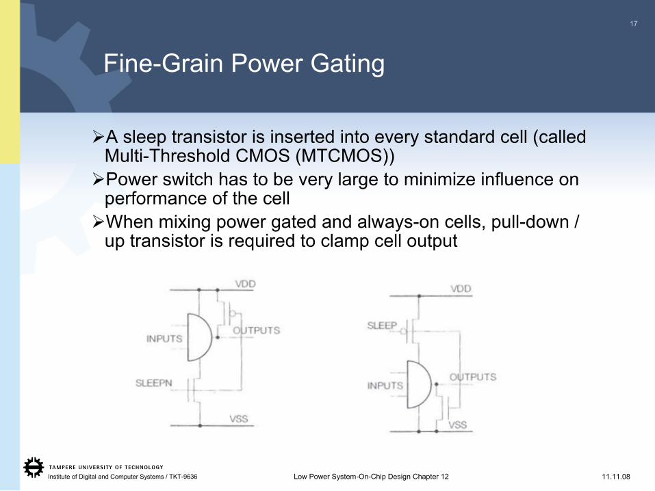
Fine-Grain Power Gating
A sleep transistor is inserted into every standard cell (called Multi-Threshold CMOS (MTCMOS))
Power switch has to be very large to minimize influence on performance of the cell
When mixing power gated and always-on cells, pull-down / up transistor is required to clamp cell output
18
Low Power System-On-Chip Design Chapter 12 11.11.08Institute of Digital and Computer Systems / TKT-9636
...Fine-Grain Power Gating
Advantages: Not sensitive to ground noise injection Small wake up latency Built-in clamp transistors eliminate all crowbar currents MTCMOS library cells can be modelled in same way as standard cell
libraries, thus conventional ASIC tools can be used for synthesizing and analysing
Drawbacks: Significant area penalty: due to sleep transistors, cell can be up to 3
times as big Requires specially designed MTCMOS library Needs significant routing and buffering resources to distribute sleep
control signal to all cells
19
Low Power System-On-Chip Design Chapter 12 11.11.08Institute of Digital and Computer Systems / TKT-9636
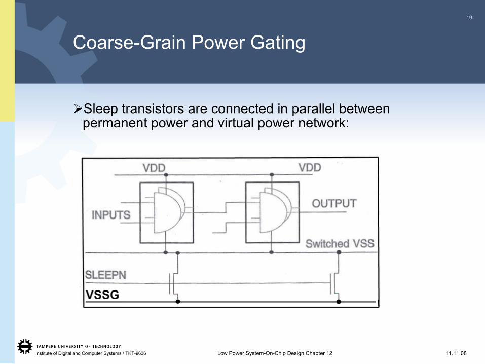
Coarse-Grain Power Gating
Sleep transistors are connected in parallel between permanent power and virtual power network:
20
Low Power System-On-Chip Design Chapter 12 11.11.08Institute of Digital and Computer Systems / TKT-9636
...Coarse-Grain Power Gating
Advantages: Significantly smaller area overhead than fine-grain power gating Less sensitive to process, voltage and temperature variation in the
sleep transistors than in fine-grain power gating Can utilize existing standard cells, only few special cells need to be
added (sleep transistors, isolation cells, retention registers)
Drawbacks: Requires complex power network, power network synthesis becomes
challenging Requires in-rush current control on wake-up to prevent power supply
noise Longer wake-up latency due to charging up the virtual power network Imposes special constraints in logic and physical synthesis
21
Low Power System-On-Chip Design Chapter 12 11.11.08Institute of Digital and Computer Systems / TKT-9636
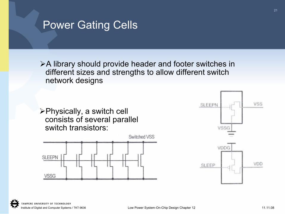
Power Gating Cells
A library should provide header and footer switches in different sizes and strengths to allow different switch network designs
Physically, a switch cell consists of several parallel switch transistors:
22
Low Power System-On-Chip Design Chapter 12 11.11.08Institute of Digital and Computer Systems / TKT-9636
References
All images are taken from: M. Keating, et al., Low Power Methodology Manual for System-on-Chip
Design, Springer, 2007