Embed Size (px)
Citation preview

For price, delivery and to place orders: Hittite Microwave Corporation, 2 Elizabeth Drive, Chelmsford, MA 01824Phone: 978-250-3343 Fax: 978-250-3373 Order On-line at www.hittite.com
Application Support: Phone: 978-250-3343 or [email protected]
mix
er
s -
i/q m
ixe
rs
, ir
ms
& r
ec
eiv
er
s -
sm
T
1
HMC6505LC5v02.0413
GaAs MMIC I/Q UPCONVERTER5.5 - 8.6 GHz
General Description
FeaturesTypical Applications
The Hmc6505Lc5 is a compact GaAs mmic i/q upconverter in a leadless roHs compliant smT package. This device provides a small signal con-version gain of 15 dB with 22 dBc of sideband rejection. The Hmc6505Lc5 utilizes a rF amplifier preceded by an i/q mixer where the LO is driven by a driver amplifier. iF1 and iF2 mixer inputs are provided and an external 90° hybrid is needed to select the required sideband. The i/q mixer topology reduces the need for filtering of the unwanted sideband. The Hmc6505Lc5 is a much smaller alternative to hybrid style single sideband upconverter assemblies and it eliminates the need for wire bonding by allowing the use of surface mount man-ufacturing techniques.
Electrical Specifications, TA = +25°C, IF = 350 MHz, LO = +4 dBm, Vdd2, 3 = +5V, Idd2 + Idd3 = 120 mA, Vdd1 = +5V, Idd1 = 125 mA [1][2][6]
Parameter min. Typ. max. min. Typ. max. Units
Frequency range, rF 5.5 - 7 7 - 8.6 GHz
Frequency range, LO 5 - 10 6.5 - 11.6 GHz
Frequency range, iF Dc - 3 Dc - 3 GHz
conversion Gain [5] 12 15 11 14 dB
sideband rejection 18 22 18 22 dBc
1 dB compression (Output) 21 22 dBm
iP3 (Output) 31 35 31 35 dBm
LO / rF rejection [3] [4] 7 10 11 14 dBc
rF return Loss 16 17 dB
LO return Loss 8 9 dB
iF1 return Loss 10 10 dB
iF2 return Loss 8 8 dB
supply current idd1 125 125 mA
supply current idd2 + idd3 [2] 120 120 mA
[1] Unless otherwise noted all measurements performed with high side LO, iF = 350 mHz and external iF 90° hybrid.[2] Adjust vgg between -2 to 0v to achieve idd2 + idd3 = 120 mA Typical.[3] The LO / rF rejection is defined as the LO signal level at the rF output port relative to the desired rF output signal level.[4] The LO / rF rejection data is with iF = -6 dBm.[5] Data based on subtracting out board loss and loss of hybrid.[6] +3v can also be used for vdd1.
Functional Diagram
The Hmc6505Lc5 is ideal for:
• Point-to-Point and Point-to-Multi-Point Radio
• Military Radar, EW & ELINT
• Satellite Communications
• Sensors
High conversion Gain: 15 dB
sideband rejection: 22 dBc
LO / rF rejection: 14 dBc
High Output iP3: +35 dBm
32 Lead 5x5 mm smT ceramic Package: 25 mm²
OBSOLETE

For price, delivery and to place orders: Hittite Microwave Corporation, 2 Elizabeth Drive, Chelmsford, MA 01824Phone: 978-250-3343 Fax: 978-250-3373 Order On-line at www.hittite.com
Application Support: Phone: 978-250-3343 or [email protected]
mix
er
s -
i/q m
ixe
rs
, ir
ms
& r
ec
eiv
er
s -
sm
T
2
HMC6505LC5v02.0413
GaAs MMIC I/Q UPCONVERTER5.5 - 8.6 GHz
LO Return Loss vs. Temperature
Conversion Gain, LSB vs. LO Drive [8]
RF Return Loss vs. Temperature
Conversion Gain, LSB vs. Temperature [8]
Data Taken as SSB Upconverter with External IF 90° Hybrid, IF = 350 MHz
0
4
8
12
16
20
5.5 6 6.5 7 7.5 8 8.5 9
2 dBm3 dBm4 dBm5 dBm6 dBm
CO
NV
ER
SIO
N G
AIN
(dB
)
RF FREQUENCY (GHz)
-30
-25
-20
-15
-10
-5
0
5 6 7 8 9
+25 C+85 C -40 C
RE
TU
RN
LO
SS
(dB
)
RF FREQUENCY (GHz)
-25
-20
-15
-10
-5
0
5 6 7 8 9
+25 C+85 C -40 C
RE
TU
RN
LO
SS
(dB
)
FREQUENCY (GHz)
Parameter min. Typ. max. min. Typ. max. Units
Frequency range, rF 5.5 - 7 7 - 8.6 GHz
Frequency range, LO 5 - 10 6.5 - 11.6 GHz
Frequency range, iF Dc - 3 Dc - 3 GHz
Dynamic range 18 20 18 20 dB
v control -4 0 -4 0 v
LO Power -2 3 10 -2 3 10 dBm
Gain Flatness (150 mHz segments) 0.5 0.5 dB
Noise Figure (Min Attenuation) [7] 11.5 12 dB
[1] Unless otherwise noted all measurements performed with high side LO, iF = 350 mHz and external iF 90° hybrid.[7] Noise Figure measurement performed with high side LO, IF = 2500 MHz and external IF 90° hybrid.
Electrical Specifications, (continued) [1]
[8] Board loss and Hybrid loss not subtracted out.
0
4
8
12
16
20
5.5 6 6.5 7 7.5 8 8.5 9
+25 C+85 C -40 C
CO
NV
ER
SIO
N G
AIN
(dB
)
RF FREQUENCY (GHz)
OBSOLETE

For price, delivery and to place orders: Hittite Microwave Corporation, 2 Elizabeth Drive, Chelmsford, MA 01824Phone: 978-250-3343 Fax: 978-250-3373 Order On-line at www.hittite.com
Application Support: Phone: 978-250-3343 or [email protected]
mix
er
s -
i/q m
ixe
rs
, ir
ms
& r
ec
eiv
er
s -
sm
T
3
HMC6505LC5v02.0413
GaAs MMIC I/Q UPCONVERTER5.5 - 8.6 GHz
Input P1dB, LSB vs. Temperature Output P1dB, LSB vs. Temperature
Input IP3, LSB vs. Temperature Output IP3, LSB vs. Temperature
Data Taken as SSB Upconverter with External IF 90° Hybrid, IF = 350 MHz
5
10
15
20
25
30
5.5 6 6.5 7 7.5 8 8.5 9
+25 C+85 C -40 C
IP3
(dB
m)
RF FREQUENCY (GHz)
20
25
30
35
40
45
5.5 6 6.5 7 7.5 8 8.5 9
+25 C+85 C -40 C
IP3
(dB
m)
RF FREQUENCY (GHz)
0
2
4
6
8
10
12
14
16
5.5 6 6.5 7 7.5 8 8.5 9
+25 C+85 C -40 C
P1d
B (
dBm
)
RF FREQUENCY (GHz)
14
16
18
20
22
24
26
5.5 6 6.5 7 7.5 8 8.5 9
+25 C+85 C -40 C
P1d
B (
dBm
)
RF FREQUENCY (GHz)
-30
-25
-20
-15
-10
-5
0
0 1 2 3 4
IF1IF2
RE
TU
RN
LO
SS
(dB
)
FREQUENCY (GHz)
IF Return Loss [9]
0
5
10
15
20
25
30
35
40
5.5 6 6.5 7 7.5 8 8.5 9
+25 C+85 C -40 C
SID
E B
AN
D R
EJE
CT
ION
(dB
c)
RF FREQUENCY (GHz)
Sideband Rejection vs. Temperature
[9] Data taken without external iF 90° hybrid
OBSOLETE

For price, delivery and to place orders: Hittite Microwave Corporation, 2 Elizabeth Drive, Chelmsford, MA 01824Phone: 978-250-3343 Fax: 978-250-3373 Order On-line at www.hittite.com
Application Support: Phone: 978-250-3343 or [email protected]
mix
er
s -
i/q m
ixe
rs
, ir
ms
& r
ec
eiv
er
s -
sm
T
4
HMC6505LC5v02.0413
GaAs MMIC I/Q UPCONVERTER5.5 - 8.6 GHz
Conversion Gain, LSB vs. Control Voltage [8] Input IP3, LSB vs. Control Voltage
LO/RF Rejection, LSB Isolation
Data Taken as SSB Upconverter with External IF 90° Hybrid, IF = 350 MHz
-15
-10
-5
0
5
10
15
20
-4 -3.5 -3 -2.5 -2 -1.5 -1 -0.5 0
5.5 GHz6.5 GHz7.5 GHz8.5 GHz
CO
NV
ER
SIO
N G
AIN
(dB
)
VCTRL (V)
15
18
21
24
27
30
-4 -3.5 -3 -2.5 -2 -1.5 -1 -0.5 0
5.5 GHz6.5 GHz7.5 GHz8.5 GHz
IP3
(dB
m)
VCTRL (V)
0
5
10
15
20
25
5.5 6 6.5 7 7.5 8 8.5 9
+25 C+85 C -40 C
LO/R
F R
EJE
CT
ION
(dB
c)
FREQUENCY (GHz)
-20
-15
-10
-5
0
5 6 7 8 9
LO/IF1LO/IF2
ISO
LAT
ION
(dB
)
FREQUENCY (GHz)
[8] Board loss and Hybrid loss not subtracted out.
OBSOLETE

For price, delivery and to place orders: Hittite Microwave Corporation, 2 Elizabeth Drive, Chelmsford, MA 01824Phone: 978-250-3343 Fax: 978-250-3373 Order On-line at www.hittite.com
Application Support: Phone: 978-250-3343 or [email protected]
mix
er
s -
i/q m
ixe
rs
, ir
ms
& r
ec
eiv
er
s -
sm
T
5
HMC6505LC5v02.0413
GaAs MMIC I/Q UPCONVERTER5.5 - 8.6 GHz
Input P1dB, LSB vs. Temperature
Conversion Gain, LSB vs. LO Drive [8]
Sideband Rejection vs. Temperature
Output P1dB, LSB vs. Temperature Input IP3, LSB vs. Temperature
Conversion Gain, LSB vs. Temperature [8]
Data Taken as SSB Upconverter with External IF 90° Hybrid, IF = 2500 MHz
0
4
8
12
16
20
5.5 6 6.5 7 7.5 8 8.5 9
+25 C+85 C -40 C
CO
NV
ER
SIO
N G
AIN
(dB
)
RF FREQUENCY (GHz)
0
4
8
12
16
20
5.5 6 6.5 7 7.5 8 8.5 9
2 dBm3 dBm4 dBm5 dBm6 dBm
CO
NV
ER
SIO
N G
AIN
(dB
)
RF FREQUENCY (GHz)
10
15
20
25
30
35
40
5.5 6 6.5 7 7.5 8 8.5 9
+25 C+85 C -40 C
SID
E B
AN
D R
EJE
CT
ION
(dB
c)
RF FREQUENCY (GHz)
10
15
20
25
30
35
5.5 6 6.5 7 7.5 8 8.5 9
+25 C+85 C -40 C
IP3
(dB
m)
RF FREQUENCY (GHz)
0
2
4
6
8
10
12
14
16
5.5 6 6.5 7 7.5 8 8.5 9
+25 C+85 C -40 C
P1d
B (
dBm
)
RF FREQUENCY (GHz)
14
16
18
20
22
24
26
5.5 6 6.5 7 7.5 8 8.5 9
+25 C+85 C -40 C
P1d
B (
dBm
)
RF FREQUENCY (GHz)
[8] Board loss and Hybrid loss not subtracted out.
OBSOLETE

For price, delivery and to place orders: Hittite Microwave Corporation, 2 Elizabeth Drive, Chelmsford, MA 01824Phone: 978-250-3343 Fax: 978-250-3373 Order On-line at www.hittite.com
Application Support: Phone: 978-250-3343 or [email protected]
mix
er
s -
i/q m
ixe
rs
, ir
ms
& r
ec
eiv
er
s -
sm
T
6
HMC6505LC5v02.0413
GaAs MMIC I/Q UPCONVERTER5.5 - 8.6 GHz
Conversion Gain, LSB vs. Control Voltage [8]
Input IP3, LSB vs. Control Voltage
Output IP3, LSB vs. Temperature
Data Taken as SSB Upconverter with External IF 90° Hybrid, IF = 2500 MHz
20
25
30
35
40
45
5.5 6 6.5 7 7.5 8 8.5 9
+25 C+85 C -40 C
IP3
(dB
m)
RF FREQUENCY (GHz)
-15
-10
-5
0
5
10
15
-4 -3.5 -3 -2.5 -2 -1.5 -1 -0.5 0
5.5 GHz6.5 GHz7.5 GHz8.5 GHz
CO
NV
ER
SIO
N G
AIN
(dB
)
VCTRL (V)
10
14
18
22
26
30
-4 -3.5 -3 -2.5 -2 -1.5 -1 -0.5 0
5.5 GHz6.5 GHz7.5 GHz8.5 GHz
IP3
(dB
m)
VCTRL (V)
Noise Figure, LSB vs. TemperatureMinimum Attenuation
0
2
4
6
8
10
12
14
16
5.5 6 6.5 7 7.5 8 8.5 9
+25 C+85 C -40 CN
OIS
E F
IGU
RE
(dB
)
FREQUENCY (GHz)
[8] Board loss and Hybrid loss not subtracted out.
OBSOLETE

For price, delivery and to place orders: Hittite Microwave Corporation, 2 Elizabeth Drive, Chelmsford, MA 01824Phone: 978-250-3343 Fax: 978-250-3373 Order On-line at www.hittite.com
Application Support: Phone: 978-250-3343 or [email protected]
mix
er
s -
i/q m
ixe
rs
, ir
ms
& r
ec
eiv
er
s -
sm
T
7
HMC6505LC5v02.0413
GaAs MMIC I/Q UPCONVERTER5.5 - 8.6 GHz
Conversion Gain, USB vs. Temperature [8]
Data Taken as SSB Upconverter with External IF 90° Hybrid, IF = 350 MHz
Conversion Gain, USB vs. LO Drive [8]
Sideband Rejection vs. Temperature Input P1dB, USB vs. Temperature
Output P1dB, USB vs. Temperature Input IP3, USB vs. Temperature
0
4
8
12
16
20
5.5 6 6.5 7 7.5 8 8.5 9
+25 C+85 C -40 C
CO
NV
ER
SIO
N G
AIN
(dB
)
RF FREQUENCY (GHz)
0
4
8
12
16
20
5.5 6 6.5 7 7.5 8 8.5 9
2 dBm3 dBm4 dBm5 dBm6 dBm
CO
NV
ER
SIO
N G
AIN
(dB
)
RF FREQUENCY (GHz)
0
5
10
15
20
25
30
5.5 6 6.5 7 7.5 8 8.5 9
+25 C+85 C -40 C
SID
E B
AN
D R
EJE
CT
ION
(dB
c)
RF FREQUENCY (GHz)
10
15
20
25
30
35
5.5 6 6.5 7 7.5 8 8.5 9
+25 C+85 C -40 C
IP3
(dB
m)
RF FREQUENCY (GHz)
0
2
4
6
8
10
12
14
16
5.5 6 6.5 7 7.5 8 8.5 9
+25 C+85 C -40 C
P1d
B (
dBm
)
RF FREQUENCY (GHz)
14
16
18
20
22
24
26
5.5 6 6.5 7 7.5 8 8.5 9
+25 C+85 C -40 C
P1d
B (
dBm
)
RF FREQUENCY (GHz)
[8] Board loss and Hybrid loss not subtracted out.
OBSOLETE

For price, delivery and to place orders: Hittite Microwave Corporation, 2 Elizabeth Drive, Chelmsford, MA 01824Phone: 978-250-3343 Fax: 978-250-3373 Order On-line at www.hittite.com
Application Support: Phone: 978-250-3343 or [email protected]
mix
er
s -
i/q m
ixe
rs
, ir
ms
& r
ec
eiv
er
s -
sm
T
8
HMC6505LC5v02.0413
GaAs MMIC I/Q UPCONVERTER5.5 - 8.6 GHz
Data Taken as SSB Upconverter with External IF 90° Hybrid, IF = 350 MHz
Output IP3, USB vs. TemperatureConversion Gain, USB vs. Control Voltage [8]
Input IP3, USB vs. Control Voltage
20
25
30
35
40
45
5.5 6 6.5 7 7.5 8 8.5 9
+25 C+85 C -40 C
IP3
(dB
m)
RF FREQUENCY (GHz)
-15
-10
-5
0
5
10
15
-4 -3.5 -3 -2.5 -2 -1.5 -1 -0.5 0
5.5 GHz6.5 GHz7.5 GHz8.5 GHz
CO
NV
ER
SIO
N G
AIN
(dB
)
VCTRL (V)
10
15
20
25
30
35
40
-4 -3.5 -3 -2.5 -2 -1.5 -1 -0.5 0
5.5 GHz6.5 GHz7.5 GHz8.5 GHz
IP3
(dB
m)
VCTRL (V)
LO/RF Rejection, USB
0
5
10
15
20
25
5.5 6 6.5 7 7.5 8 8.5 9
+25 C+85 C -40 C
LO/R
F R
EJE
CT
ION
(dB
c)
FREQUENCY (GHz)
[8] Board loss and Hybrid loss not subtracted out.
OBSOLETE

For price, delivery and to place orders: Hittite Microwave Corporation, 2 Elizabeth Drive, Chelmsford, MA 01824Phone: 978-250-3343 Fax: 978-250-3373 Order On-line at www.hittite.com
Application Support: Phone: 978-250-3343 or [email protected]
mix
er
s -
i/q m
ixe
rs
, ir
ms
& r
ec
eiv
er
s -
sm
T
9
HMC6505LC5v02.0413
GaAs MMIC I/Q UPCONVERTER5.5 - 8.6 GHz
Data Taken as SSB Upconverter with External IF 90° Hybrid, IF = 2500 MHz
Conversion Gain, USB vs. Temperature [8] Conversion Gain, USB vs. LO Drive [8]
Sideband Rejection vs. Temperature Input P1dB, USB vs. Temperature
Output P1dB, USB vs. Temperature Input IP3, USB vs. Temperature
0
4
8
12
16
20
5.5 6 6.5 7 7.5 8 8.5 9
+25 C+85 C -40 C
CO
NV
ER
SIO
N G
AIN
(dB
)
RF FREQUENCY (GHz)
0
4
8
12
16
20
5.5 6 6.5 7 7.5 8 8.5 9
2 dBm3 dBm4 dBm5 dBm6 dBm
CO
NV
ER
SIO
N G
AIN
(dB
)
RF FREQUENCY (GHz)
30
40
50
60
70
80
5.5 6 6.5 7 7.5 8 8.5 9
+25 C+85 C -40 C
SID
E B
AN
D R
EJE
CT
ION
(dB
c)
RF FREQUENCY (GHz)
0
5
10
15
20
25
30
35
5.5 6 6.5 7 7.5 8 8.5 9
+25 C+85 C -40 C
IP3
(dB
m)
RF FREQUENCY (GHz)
0
2
4
6
8
10
12
14
16
5.5 6 6.5 7 7.5 8 8.5 9
+25 C+85 C -40 C
P1d
B (
dBm
)
RF FREQUENCY (GHz)
14
16
18
20
22
24
26
5.5 6 6.5 7 7.5 8 8.5 9
+25 C+85 C -40 C
P1d
B (
dBm
)
RF FREQUENCY (GHz)
[8] Board loss and Hybrid loss not subtracted out.
OBSOLETE

For price, delivery and to place orders: Hittite Microwave Corporation, 2 Elizabeth Drive, Chelmsford, MA 01824Phone: 978-250-3343 Fax: 978-250-3373 Order On-line at www.hittite.com
Application Support: Phone: 978-250-3343 or [email protected]
mix
er
s -
i/q m
ixe
rs
, ir
ms
& r
ec
eiv
er
s -
sm
T
10
HMC6505LC5v02.0413
GaAs MMIC I/Q UPCONVERTER5.5 - 8.6 GHz
Data Taken as SSB Upconverter with External IF 90° Hybrid, IF = 2500 MHz
Output IP3, USB vs. TemperatureConversion Gain, USB vs. Control Voltage [8]
Input IP3, USB vs. Control Voltage
-40
-30
-20
-10
0
10
20
-4 -3.5 -3 -2.5 -2 -1.5 -1 -0.5 0
5.5 GHz6.5 GHz7.5 GHz8.5 GHz
CO
NV
ER
SIO
N G
AIN
(dB
)
VCTRL (V)
0
5
10
15
20
25
30
-4 -3.5 -3 -2.5 -2 -1.5 -1 -0.5 0
5.5 GHz6.5 GHz7.5 GHz8.5 GHz
IP3
(dB
m)
VCTRL (V)
0
4
8
12
16
20
5.5 6 6.5 7 7.5 8 8.5 9
+25 C+85 C -40 C
CO
NV
ER
SIO
N G
AIN
(dB
)
RF FREQUENCY (GHz)
[8] Board loss and Hybrid loss not subtracted out.
OBSOLETE

For price, delivery and to place orders: Hittite Microwave Corporation, 2 Elizabeth Drive, Chelmsford, MA 01824Phone: 978-250-3343 Fax: 978-250-3373 Order On-line at www.hittite.com
Application Support: Phone: 978-250-3343 or [email protected]
mix
er
s -
i/q m
ixe
rs
, ir
ms
& r
ec
eiv
er
s -
sm
T
11
HMC6505LC5v02.0413
GaAs MMIC I/Q UPCONVERTER5.5 - 8.6 GHz
MxN Spurious Outputs [1][2] MxN Spurious Outputs [1][3]
nLO
miF 0 1 2 3 4
0 x 17.3 35.1 57.5 62.6
+1 80.6 0 39.6 66.4 93.3
+2 49.9 64.3 40.6 72.3 91.5
+3 96.7 57.8 87.4 78.5 89.8
+4 88.5 100.8 89.3 94.2 91.7
iF = 0.35 GHz @ -6 dBm
LO = 8.5 GHz @ 0 dBm
nLO
miF 0 1 2 3 4
0 x 17.3 35.1 56.5 62.7
-1 80.6 0 42.8 62.9 93
-2 49.9 53.3 39.3 72.9 90.3
-3 96.9 56 90 75 93
-4 88.2 101.9 89.4 96.1 91.1
iF = 0.35 GHz @ -6 dBm
LO = 8.5 GHz @ 0 dBm
[1] Data taken without external iF 90° hybrid[2] All values in dBc below rF power level (LO + iF) UsB[3] All values in dBc below rF power level (LO - iF) LsB
nLO
miF 0 1 2 3 4
0 x 15.1 36.4 50.4 61.5
+1 66.7 0 42.9 56.5 83.2
+2 49.2 47.1 39.9 76.5 84.6
+3 95.2 58.9 79.4 76 94.2
+4 86.9 102.5 86.5 96.8 96.1
iF = 0.35 GHz @ -6 dBm
LO = 7.7 GHz @ 0 dBm
nLO
miF 0 1 2 3 4
0 x 15 36.4 50.6 60.1
-1 66.6 0 48.2 51.4 82.8
-2 49.2 47 38.1 79.7 79.9
-3 95.9 56.7 86.7 75.4 93.1
-4 86.9 94 88.3 97.4 93.8
iF = 0.35 GHz @ -6 dBm
LO = 7.7 GHz @ 0 dBm
nLO
miF 0 1 2 3 4
0 x 11.6 23.6 38.4 60.1
+1 59.8 0 42.9 45.4 70.9
+2 48.5 50.4 39.4 79.9 76.7
+3 86.9 61 87.5 76.2 94.3
+4 85.2 82.4 86.2 97 95.7
iF = 0.35 GHz @ -6 dBm
LO = 7.0 GHz @ 0 dBm
nLO
miF 0 1 2 3 4
0 x 11.6 23.5 38.3 58.7
-1 59.7 0 46.7 36.9 73.4
-2 48.6 53 37.7 75.2 69.1
-3 87 58 75 70.9 91.1
-4 84.8 87 83.6 99.5 93.1
iF = 0.35 GHz @ -6 dBm
LO = 7.0 GHz @ 0 dBm
OBSOLETE
For price, delivery and to place orders: Hittite Microwave Corporation, 2 Elizabeth Drive, Chelmsford, MA 01824Phone: 978-250-3343 Fax: 978-250-3373 Order On-line at www.hittite.com
Application Support: Phone: 978-250-3343 or [email protected]
mix
er
s -
i/q m
ixe
rs
, ir
ms
& r
ec
eiv
er
s -
sm
T
12
HMC6505LC5v02.0413
GaAs MMIC I/Q UPCONVERTER5.5 - 8.6 GHz
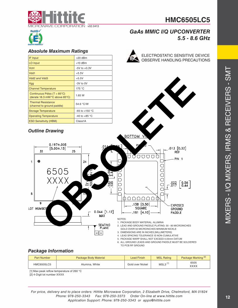
Outline Drawing
NOTES:1. PACKAGE BODY MATERIAL: ALUMINA2. LEAD AND GROUND PADDLE PLATING: 30 - 80 MICROINCHES GOLD OVER 50 MICROINCHES MINIMUM NICKLE3. DIMENSIONS ARE IN INCHES [MILLIMETERS]4. LEAD SPACING TOLERANCE IS NON-CUMULATIVE5. PACKAGE WARP SHALL NOT EXCEED 0.05mm DATUM6. ALL GROUND LEADS AND GROUND PADDLE MUST BE SOLDERED TO PCB RF GROUND
Absolute Maximum RatingsELECTROSTATIC SENSITIVE DEVICEOBSERVE HANDLING PRECAUTIONS
iF input +20 dBm
LO input +10 dBm
vctrl -5v to +0.3v
vdd1 +5.5v
vdd2 and vdd3 +5.5v
vgg -3v to 0v
channel Temperature 175 °c
continuous Pdiss (T = 85°c)(derate 18.3 mW/°c above 85°c)
1.65 W
Thermal resistance(channel to ground paddle)
54.6 °C/W
storage Temperature -65 to +150 °c
Operating Temperature -40 to +85 °c
esD sensitivity (HBm) class1A
Part Number Package Body material Lead Finish msL rating Package marking [2]
Hmc6505Lc5 Alumina, White Gold over Nickel msL3 [1] 6505xxxx
[1] max peak reflow temperature of 260 °c[2] 4-Digit lot number xxxx
Package Information
OBSOLETE

For price, delivery and to place orders: Hittite Microwave Corporation, 2 Elizabeth Drive, Chelmsford, MA 01824Phone: 978-250-3343 Fax: 978-250-3373 Order On-line at www.hittite.com
Application Support: Phone: 978-250-3343 or [email protected]
mix
er
s -
i/q m
ixe
rs
, ir
ms
& r
ec
eiv
er
s -
sm
T
13
HMC6505LC5v02.0413
GaAs MMIC I/Q UPCONVERTER5.5 - 8.6 GHz
Pin Number Function Description interface schematic
1 - 4, 6, 9 - 11, 16, 17, 19, 20, 21,
22, 24, 25, 32N/C
No connection required. The pins are not connected internally; however, all data shown herein was measured with these pins connected to rF/Dc ground externally.
5 vdd1Power supply voltage for LO amplifier. see application
circuit for required external components.
7 LOINThis pin is Ac coupled
and matched to 50 Ohms.
8, 13, 15, 27, 29, 31
GNDThese pins and package bottom must be
connected to rF/Dc ground.
12 vggGate control for rF amplifier, please follow “mmic Amplifier Biasing Procedure” application note. see application circuit
for required external components.
14 rFOUTThis pin is Ac coupled
and matched to 50 Ohms.
18, 23vdd3,vdd2
Power supply voltage for rF amplifier. see application circuit for required external components.
26 vctrl Gain control voltage for rF Amplifier
28 iF1 Differential iF input pins. For applications not requiring operation to Dc, an off chip Dc blocking capacitor should be used. For operation to Dc this pin must not source/sink more than 3mA of current or part non function and possible
part failure will result.30 iF2
Pin Descriptions
OBSOLETE

For price, delivery and to place orders: Hittite Microwave Corporation, 2 Elizabeth Drive, Chelmsford, MA 01824Phone: 978-250-3343 Fax: 978-250-3373 Order On-line at www.hittite.com
Application Support: Phone: 978-250-3343 or [email protected]
mix
er
s -
i/q m
ixe
rs
, ir
ms
& r
ec
eiv
er
s -
sm
T
14
HMC6505LC5v02.0413
GaAs MMIC I/Q UPCONVERTER5.5 - 8.6 GHz
Typical Application
c1, c3, c4, c13, c16 100 pF capacitor, 0402 Pkg.
c5, c7, c8, c14, c17 1000 pF capacitor, 0603 Pkg.
c9, c11, c12, c15, c18 2.2 µF capacitor, case A Pkg.OBSOLETE

For price, delivery and to place orders: Hittite Microwave Corporation, 2 Elizabeth Drive, Chelmsford, MA 01824Phone: 978-250-3343 Fax: 978-250-3373 Order On-line at www.hittite.com
Application Support: Phone: 978-250-3343 or [email protected]
mix
er
s -
i/q m
ixe
rs
, ir
ms
& r
ec
eiv
er
s -
sm
T
15
HMC6505LC5v02.0413
GaAs MMIC I/Q UPCONVERTER5.5 - 8.6 GHz
Evaluation PCB
The circuit board used in the application should use rF circuit design techniques. signal lines should have 50 Ohm impedance while the package ground leads and exposed paddle should be connected directly to the ground plane similar to that shown. A sufficient number of via holes should be used to connect the top and bottom ground planes. The evaluation circuit board shown is available from Hittite upon request.
List of Materials for Evaluation PCB Eval01-HMC6505LC5 [1]
item Description
J1, J2 smA connector
J3, J4 K-connector sri
J5, J6, J8, J9 Dc Pins
c1, c3, c4, c13, c16 100 pF capacitor, 0402 Pkg.
c5, c7, c8, c14, c17 1000 pF capacitor, 0603 Pkg.
c9, c11, c12, c15, c18 2.2 µF capacitor, case A
U1 Hmc6505Lc5 Upconverter
PcB [2] 125487 evaluation Board
[1] reference this number when ordering complete evaluation PcB
[2] circuit Board material: Arlon 25Fr, Fr4 or rogers 4350
OBSOLETE

For price, delivery and to place orders: Hittite Microwave Corporation, 2 Elizabeth Drive, Chelmsford, MA 01824Phone: 978-250-3343 Fax: 978-250-3373 Order On-line at www.hittite.com
Application Support: Phone: 978-250-3343 or [email protected]
mix
er
s -
i/q m
ixe
rs
, ir
ms
& r
ec
eiv
er
s -
sm
T
16
HMC6505LC5v02.0413
GaAs MMIC I/Q UPCONVERTER5.5 - 8.6 GHz
Notes:
OBSOLETE