Embed Size (px)
Citation preview
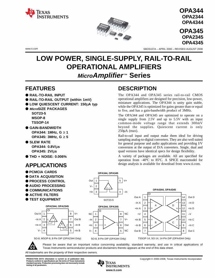
LOW POWER, SINGLE-SUPPLY, RAIL-TO-RAILOPERATIONAL AMPLIFIERS
MicroAmplifier ™ Series
FEATURES RAIL-TO-RAIL INPUT RAIL-TO-RAIL OUTPUT (within 1mV) LOW QUIESCENT CURRENT: 150µA typ MicroSIZE PACKAGES
SOT23-5MSOP-8TSSOP-14
GAIN-BANDWIDTHOPA344: 1MHz, G ≥ 1OPA345: 3MHz, G ≥ 5
SLEW RATEOPA344: 0.8V/µsOPA345: 2V/µs
THD + NOISE: 0.006%
APPLICATIONS PCMCIA CARDS DATA ACQUISITION PROCESS CONTROL AUDIO PROCESSING COMMUNICATIONS ACTIVE FILTERS TEST EQUIPMENT
DESCRIPTIONThe OPA344 and OPA345 series rail-to-rail CMOSoperational amplifiers are designed for precision, low-power,miniature applications. The OPA344 is unity gain stable,while the OPA345 is optimized for gains greater than or equalto five, and has a gain-bandwidth product of 3MHz.The OPA344 and OPA345 are optimized to operate on asingle supply from 2.5V and up to 5.5V with an inputcommon-mode voltage range that extends 300mVbeyond the supplies. Quiescent current is only250µA (max).
Rail-to-rail input and output make them ideal for drivingsampling analog-to-digital converters. They are also well suitedfor general purpose and audio applications and providing I/Vconversion at the output of D/A converters. Single, dual andquad versions have identical specs for design flexibility.
A variety of packages are available. All are specified foroperation from –40ºC to 85ºC. A SPICE macromodel fordesign analysis is available for download from www.ti.com.
OPA345OPA2345OPA4345
OPA344OPA2344OPA4344
1
2
3
5
4
V+
–In
Out
V–
+In
OPA344, OPA345
SOT23-5
1
2
3
4
8
7
6
5
NC
V+
Out
NC
NC
–In
+In
V–
OPA344, OPA345
SO-8, 8-Pin DIP (OPA344 Only)
1
2
3
4
8
7
6
5
V+
Out B
–In B
+In B
Out A
–In A
+In A
V–
OPA2344, OPA2345
SO-8, MSOP-8, 8-Pin DIP (OPA2344 Only)
A
B
1
2
3
4
5
6
7
14
13
12
11
10
9
8
Out D
–In D
+In D
–V
+In C
–In C
Out C
Out A
–In A
+In A
+V
+In B
–In B
Out B
OPA4344, OPA4345
TSSOP-14, SO-14, 14-PIn DIP (OPA4344 Only)
A D
B C
®OPA342
OPA4344OPA344
OPA345
www.ti.com
www.ti.com
PRODUCTION DATA information is current as of publication date.Products conform to specifications per the terms of Texas Instrumentsstandard warranty. Production processing does not necessarily includetesting of all parameters.
Copyright © 2000-2008, Texas Instruments Incorporated
Please be aware that an important notice concerning availability, standard warranty, and use in critical applications ofTexas Instruments semiconductor products and disclaimers thereto appears at the end of this data sheet.
All trademarks are the property of their respective owners.
SBOS107A – APRIL 2000 – REVISED AUGUST 2008
www.ti.com
OPA344, 2344, 4344OPA345, 2345, 43452
SBOS107A
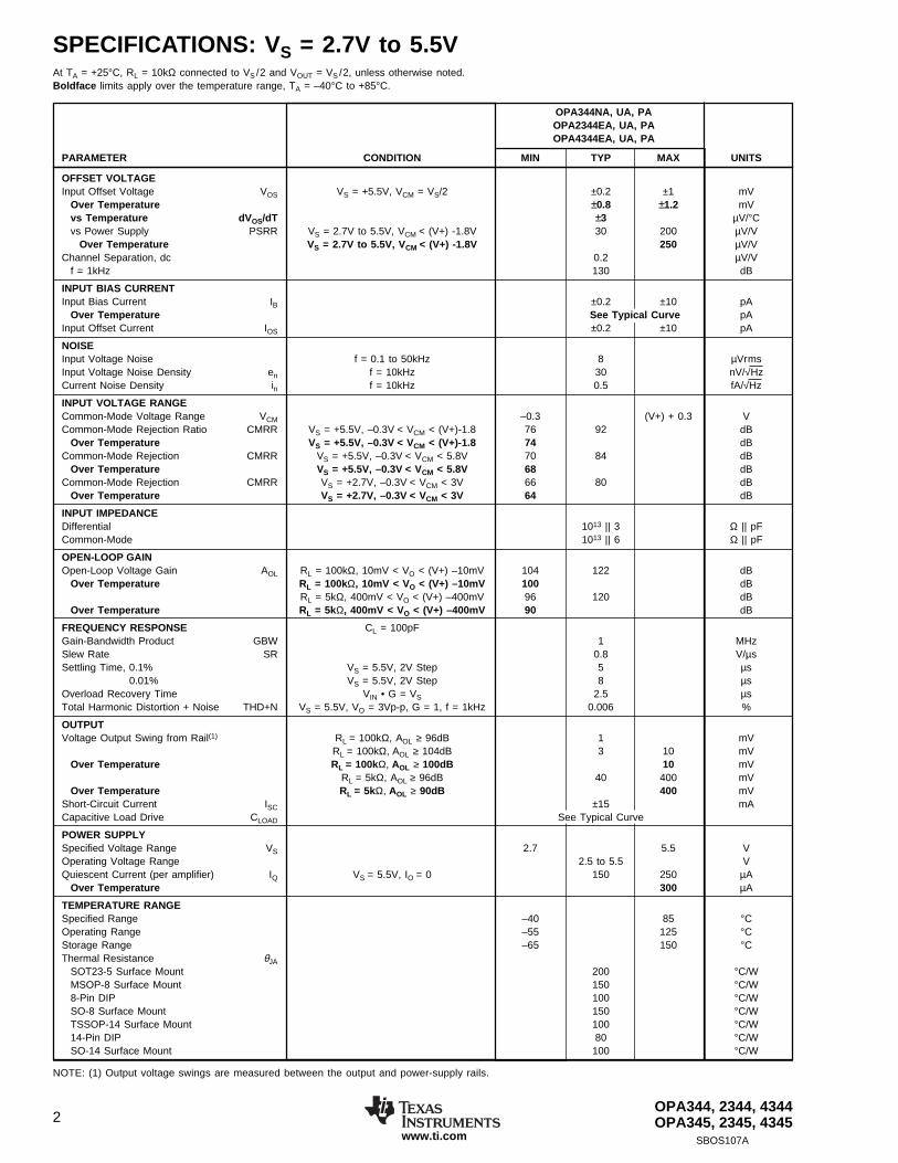
SPECIFICATIONS: VS = 2.7V to 5.5VAt TA = +25°C, RL = 10kΩ connected to VS /2 and VOUT = VS /2, unless otherwise noted.Boldface limits apply over the temperature range, TA = –40°C to +85°C.
OPA344NA, UA, PAOPA2344EA, UA, PAOPA4344EA, UA, PA
PARAMETER CONDITION MIN TYP MAX UNITS
OFFSET VOLTAGEInput Offset Voltage VOS VS = +5.5V, VCM = VS/2 ±0.2 ±1 mV
Over Temperature ±0.8 ±1.2 mVvs Temperature dVOS/dT ±3 µV/°Cvs Power Supply PSRR VS = 2.7V to 5.5V, VCM < (V+) -1.8V 30 200 µV/V
Over Temperature VS = 2.7V to 5.5V, VCM < (V+) -1.8V 250 µV/VChannel Separation, dc 0.2 µV/V
f = 1kHz 130 dB
INPUT BIAS CURRENTInput Bias Current IB ±0.2 ±10 pA
Over Temperature See Typical Curve pAInput Offset Current IOS ±0.2 ±10 pA
NOISEInput Voltage Noise f = 0.1 to 50kHz 8 µVrmsInput Voltage Noise Density en f = 10kHz 30 nV/√HzCurrent Noise Density in f = 10kHz 0.5 fA/√Hz
INPUT VOLTAGE RANGECommon-Mode Voltage Range VCM –0.3 (V+) + 0.3 VCommon-Mode Rejection Ratio CMRR VS = +5.5V, –0.3V < VCM < (V+)-1.8 76 92 dB
Over Temperature VS = +5.5V, –0.3V < VCM < (V+)-1.8 74 dBCommon-Mode Rejection CMRR VS = +5.5V, –0.3V < VCM < 5.8V 70 84 dB
Over Temperature VS = +5.5V, –0.3V < VCM < 5.8V 68 dBCommon-Mode Rejection CMRR VS = +2.7V, –0.3V < VCM < 3V 66 80 dB
Over Temperature VS = +2.7V, –0.3V < VCM < 3V 64 dB
INPUT IMPEDANCEDifferential 1013 || 3 Ω || pFCommon-Mode 1013 || 6 Ω || pF
OPEN-LOOP GAINOpen-Loop Voltage Gain AOL RL = 100kΩ, 10mV < VO < (V+) –10mV 104 122 dB
Over Temperature RL = 100kΩ, 10mV < VO < (V+) –10mV 100 dBRL = 5kΩ, 400mV < VO < (V+) –400mV 96 120 dB
Over Temperature RL = 5kΩ, 400mV < VO < (V+) –400mV 90 dB
FREQUENCY RESPONSE CL = 100pFGain-Bandwidth Product GBW 1 MHzSlew Rate SR 0.8 V/µsSettling Time, 0.1% VS = 5.5V, 2V Step 5 µs
0.01% VS = 5.5V, 2V Step 8 µsOverload Recovery Time VIN • G = VS 2.5 µsTotal Harmonic Distortion + Noise THD+N VS = 5.5V, VO = 3Vp-p, G = 1, f = 1kHz 0.006 %
OUTPUTVoltage Output Swing from Rail(1) RL = 100kΩ, AOL ≥ 96dB 1 mV
RL = 100kΩ, AOL ≥ 104dB 3 10 mVOver Temperature RL = 100kΩ, AOL ≥ 100dB 10 mV
RL = 5kΩ, AOL ≥ 96dB 40 400 mVOver Temperature RL = 5kΩ, AOL ≥ 90dB 400 mV
Short-Circuit Current ISC ±15 mACapacitive Load Drive CLOAD See Typical Curve
POWER SUPPLYSpecified Voltage Range VS 2.7 5.5 VOperating Voltage Range 2.5 to 5.5 VQuiescent Current (per amplifier) IQ VS = 5.5V, IO = 0 150 250 µA
Over Temperature 300 µA
TEMPERATURE RANGESpecified Range –40 85 °COperating Range –55 125 °CStorage Range –65 150 °CThermal Resistance θJA
SOT23-5 Surface Mount 200 °C/WMSOP-8 Surface Mount 150 °C/W8-Pin DIP 100 °C/WSO-8 Surface Mount 150 °C/WTSSOP-14 Surface Mount 100 °C/W14-Pin DIP 80 °C/WSO-14 Surface Mount 100 °C/W
NOTE: (1) Output voltage swings are measured between the output and power-supply rails.
www.ti.comSBOS107A
OPA344, 2344, 4344OPA345, 2345, 4345 3
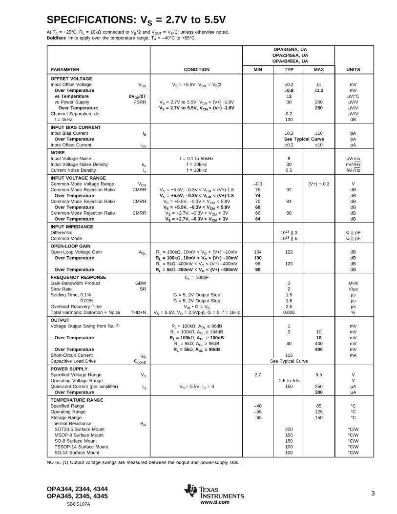
SPECIFICATIONS: VS = 2.7V to 5.5VAt TA = +25°C, RL = 10kΩ connected to VS /2 and VOUT = VS /2, unless otherwise noted.Boldface limits apply over the temperature range, TA = –40°C to +85°C.
OPA345NA, UAOPA2345EA, UAOPA4345EA, UA
PARAMETER CONDITION MIN TYP MAX UNITS
OFFSET VOLTAGEInput Offset Voltage VOS VS = +5.5V, VCM = VS/2 ±0.2 ±1 mV
Over Temperature ±0.8 ±1.2 mVvs Temperature dVOS/dT ±3 µV/°Cvs Power Supply PSRR VS = 2.7V to 5.5V, VCM < (V+) -1.8V 30 200 µV/V
Over Temperature VS = 2.7V to 5.5V, VCM < (V+) -1.8V 250 µV/VChannel Separation, dc 0.2 µV/V
f = 1kHz 130 dB
INPUT BIAS CURRENTInput Bias Current IB ±0.2 ±10 pA
Over Temperature See Typical Curve pAInput Offset Current IOS ±0.2 ±10 pA
NOISEInput Voltage Noise f = 0.1 to 50kHz 8 µVrmsInput Voltage Noise Density en f = 10kHz 30 nV/√HzCurrent Noise Density in f = 10kHz 0.5 fA/√Hz
INPUT VOLTAGE RANGECommon-Mode Voltage Range VCM –0.3 (V+) + 0.3 VCommon-Mode Rejection Ratio CMRR VS = +5.5V, –0.3V < VCM < (V+)-1.8 76 92 dB
Over Temperature VS = +5.5V, –0.3V < VCM < (V+)-1.8 74 dBCommon-Mode Rejection Ratio CMRR VS = +5.5V, –0.3V < VCM < 5.8V 70 84 dB
Over Temperature VS = +5.5V, –0.3V < VCM < 5.8V 68 dBCommon-Mode Rejection Ratio CMRR VS = +2.7V, –0.3V < VCM < 3V 66 80 dB
Over Temperature VS = +2.7V, –0.3V < VCM < 3V 64 dB
INPUT IMPEDANCEDifferential 1013 || 3 Ω || pFCommon-Mode 1013 || 6 Ω || pF
OPEN-LOOP GAINOpen-Loop Voltage Gain AOL RL = 100kΩ, 10mV < VO < (V+) –10mV 104 122 dB
Over Temperature RL = 100kΩ, 10mV < VO < (V+) –10mV 100 dBRL = 5kΩ, 400mV < VO < (V+) –400mV 96 120 dB
Over Temperature RL = 5kΩ, 400mV < VO < (V+) –400mV 90 dB
FREQUENCY RESPONSE CL = 100pFGain-Bandwidth Product GBW 3 MHzSlew Rate SR 2 V/µsSettling Time, 0.1% G = 5, 2V Output Step 1.5 µs
0.01% G = 5, 2V Output Step 1.6 µsOverload Recovery Time VIN • G = VS 2.5 µsTotal Harmonic Distortion + Noise THD+N VS = 5.5V, VO = 2.5Vp-p, G = 5, f = 1kHz 0.006 %
OUTPUTVoltage Output Swing from Rail(1) RL = 100kΩ, AOL ≥ 96dB 1 mV
RL = 100kΩ, AOL ≥ 104dB 3 10 mVOver Temperature RL = 100kΩ, AOL ≥ 100dB 10 mV
RL = 5kΩ, AOL ≥ 96dB 40 400 mVOver Temperature RL = 5kΩ, AOL ≥ 90dB 400 mV
Short-Circuit Current ISC ±15 mACapacitive Load Drive CLOAD See Typical Curve
POWER SUPPLYSpecified Voltage Range VS 2.7 5.5 VOperating Voltage Range 2.5 to 5.5 VQuiescent Current (per amplifier) IQ VS = 5.5V, IO = 0 150 250 µA
Over Temperature 300 µA
TEMPERATURE RANGESpecified Range –40 85 °COperating Range –55 125 °CStorage Range –65 150 °CThermal Resistance θJA
SOT23-5 Surface Mount 200 °C/WMSOP-8 Surface Mount 150 °C/WSO-8 Surface Mount 150 °C/WTSSOP-14 Surface Mount 100 °C/WSO-14 Surface Mount 100 °C/W
NOTE: (1) Output voltage swings are measured between the output and power-supply rails.
www.ti.com
OPA344, 2344, 4344OPA345, 2345, 43454
SBOS107A
SPECIFIEDPACKAGE TEMPERATURE PACKAGE ORDERING TRANSPORT
PRODUCT PACKAGE DESIGNATOR RANGE MARKING NUMBER(2) MEDIA
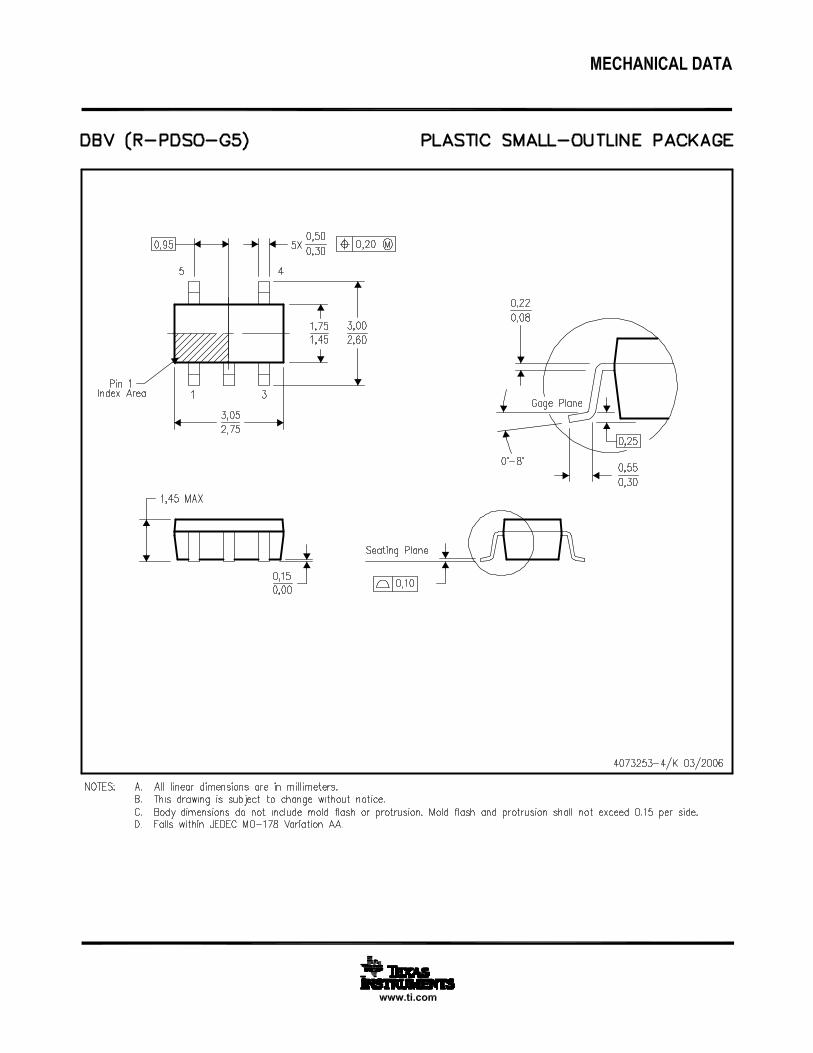
OPA344NA SOT23-5 DBV –40°C to +85°C B44 OPA344NA/250 Tape and Reel" " " " " OPA344NA/3K Tape and Reel
OPA344UA SO-8 D –40°C to +85°C OPA344UA OPA344UA Rails" " " " " OPA344UA/2K5 Tape and Reel
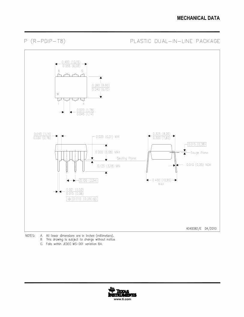
OPA344PA 8-Pin Dip P –40° C to +85°C OPA344PA OPA344PA Rails
OPA2344EA MSOP-8 DGK –40°C to +85°C C44 OPA2344EA/250 Tape and Reel" " " " " OPA2344EA/2K5 Tape and Reel
OPA2344UA SO-8 D –40°C to +85°C OPA2344UA OPA2344UA Rails" " " " " OPA2344UA/2K5 Tape and Reel
OPA2344PA 8-Pin DIP P –40°C to +85°C OPA2344PA OPA2344PA Rails
OPA4344EA TSSOP-14 PW –40°C to +85°C OPA4344EA OPA4344EA/250 Rails" " " " " OPA4344EA/2K5 Tape and Reel
OPA4344UA SO-14 D –40°C to +85°C OPA4344UA OPA4344UA Rails" " " " " OPA4344UA/2K5 Tape and Reel
OPA4344PA 14-Pin DIP N –40°C to +85°C OPA4344PA OPA4344PA Rails
OPA345NA SOT23-5 DBV –40°C to +85°C A45 OPA345NA/250 Tape and Reel" " " " " OPA345NA/3K Tape and Reel
OPA345UA SO-8 D –40°C to +85°C OPA345UA OPA345UA Rails" " " " " OPA345UA/2K5 Tape and Reel
OPA2345EA MSOP-8 DGK –40°C to +85°C B45 OPA2345EA/250 Tape and Reel" " " " " OPA2345EA/2K5 Tape and Reel
OPA2345UA SO-8 D –40°C to +85°C OPA2345UA OPA2345UA Rails" " " " " OPA2345UA/2K5 Tape and Reel
OPA4345EA TSSOP-14 PW –40°C to +85°C OPA4345EA OPA4345EA/250 Tape and Reel" " " " " OPA4345EA/2K5 Tape and Reel
OPA4345UA SO-14 D –40°C to +85°C OPA4345UA OPA4345UA Rails" " " " " OPA4345UA/2K5 Tape and Reel
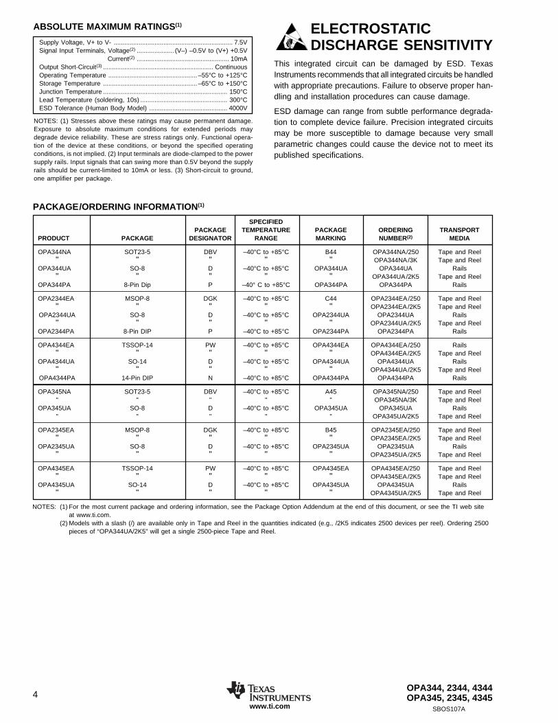
NOTES: (1) For the most current package and ordering information, see the Package Option Addendum at the end of this document, or see the TI web siteat www.ti.com.
(2) Models with a slash (/) are available only in Tape and Reel in the quantities indicated (e.g., /2K5 indicates 2500 devices per reel). Ordering 2500pieces of “OPA344UA/2K5” will get a single 2500-piece Tape and Reel.
PACKAGE/ORDERING INFORMATION(1)
Supply Voltage, V+ to V- ................................................................... 7.5VSignal Input Terminals, Voltage(2) ..................... (V–) –0.5V to (V+) +0.5V
Current(2) .................................................... 10mAOutput Short-Circuit(3) .............................................................. ContinuousOperating Temperature .................................................. –55°C to +125°CStorage Temperature .....................................................–65°C to +150°CJunction Temperature ...................................................................... 150°CLead Temperature (soldering, 10s) ................................................. 300°CESD Tolerance (Human Body Model) ............................................ 4000V
NOTES: (1) Stresses above these ratings may cause permanent damage.Exposure to absolute maximum conditions for extended periods maydegrade device reliability. These are stress ratings only. Functional opera-tion of the device at these conditions, or beyond the specified operatingconditions, is not implied. (2) Input terminals are diode-clamped to the powersupply rails. Input signals that can swing more than 0.5V beyond the supplyrails should be current-limited to 10mA or less. (3) Short-circuit to ground,one amplifier per package.
ABSOLUTE MAXIMUM RATINGS(1) ELECTROSTATICDISCHARGE SENSITIVITY
This integrated circuit can be damaged by ESD. TexasInstruments recommends that all integrated circuits be handledwith appropriate precautions. Failure to observe proper han-dling and installation procedures can cause damage.
ESD damage can range from subtle performance degrada-tion to complete device failure. Precision integrated circuitsmay be more susceptible to damage because very smallparametric changes could cause the device not to meet itspublished specifications.
www.ti.comSBOS107A
OPA344, 2344, 4344OPA345, 2345, 4345 5
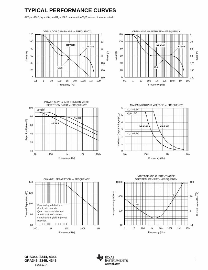
TYPICAL PERFORMANCE CURVESAt TA = +25°C, VS = +5V, and RL = 10kΩ connected to VS/2, unless otherwise noted.
POWER SUPPLY AND COMMON-MODEREJECTION RATIO vs FREQUENCY
10
Rej
ectio
n R
atio
(dB
)
Frequency (Hz)
100 1k 10k 100k
100
80
60
40
20
10
+PSRR
CMRR
–PSRR
MAXIMUM OUTPUT VOLTAGE vs FREQUENCY
10k 100k
Max
imum
Out
put V
olta
ge (
VP
P)
Frequency (Hz)
1M 10M
6
5
4
3
2
1
0
OPA344
VS = +5.5V
VS = +5V
VS = +2.7V
OPA345
CHANNEL SEPARATION vs FREQUENCY
100
Cha
nnel
Sep
arat
ion
(dB
)
Frequency (Hz)
1k 10k 100k 1M
140
120
100
80
60
Dual and quad devices.G = 1, all channels.Quad measured channelA to D or B to C—othercombinations yield improvedrejection.
VOLTAGE AND CURRENT NOISESPECTRAL DENSITY vs FREQUENCY
1
Vol
tage
Noi
se (
nV/√
Hz)
Frequency (Hz)
10 100 1k 10k 100k 1M 10M
10000
1000
100
10
Cur
rent
Noi
se (
fA/√
Hz)
100
10
1
0.1
VN
IN
OPEN-LOOP GAIN/PHASE vs FREQUENCY
0.1 1
Gai
n (d
B)
0
30
60
90
120
150
180
Pha
se (
°)
Frequency (Hz)
10 100 1k 10k 100k 1M 10M
120
100
80
60
40
20
0
Gain
PhaseOPA345
OPEN-LOOP GAIN/PHASE vs FREQUENCY
0.1 1
Gai
n (d
B)
0
30
60
90
120
150
180
Pha
se (
°)
Frequency (Hz)
10 100 1k 10k 100k 1M 10M
120
100
80
60
40
20
0
Gain
PhaseOPA344
www.ti.com
OPA344, 2344, 4344OPA345, 2345, 43456
SBOS107A
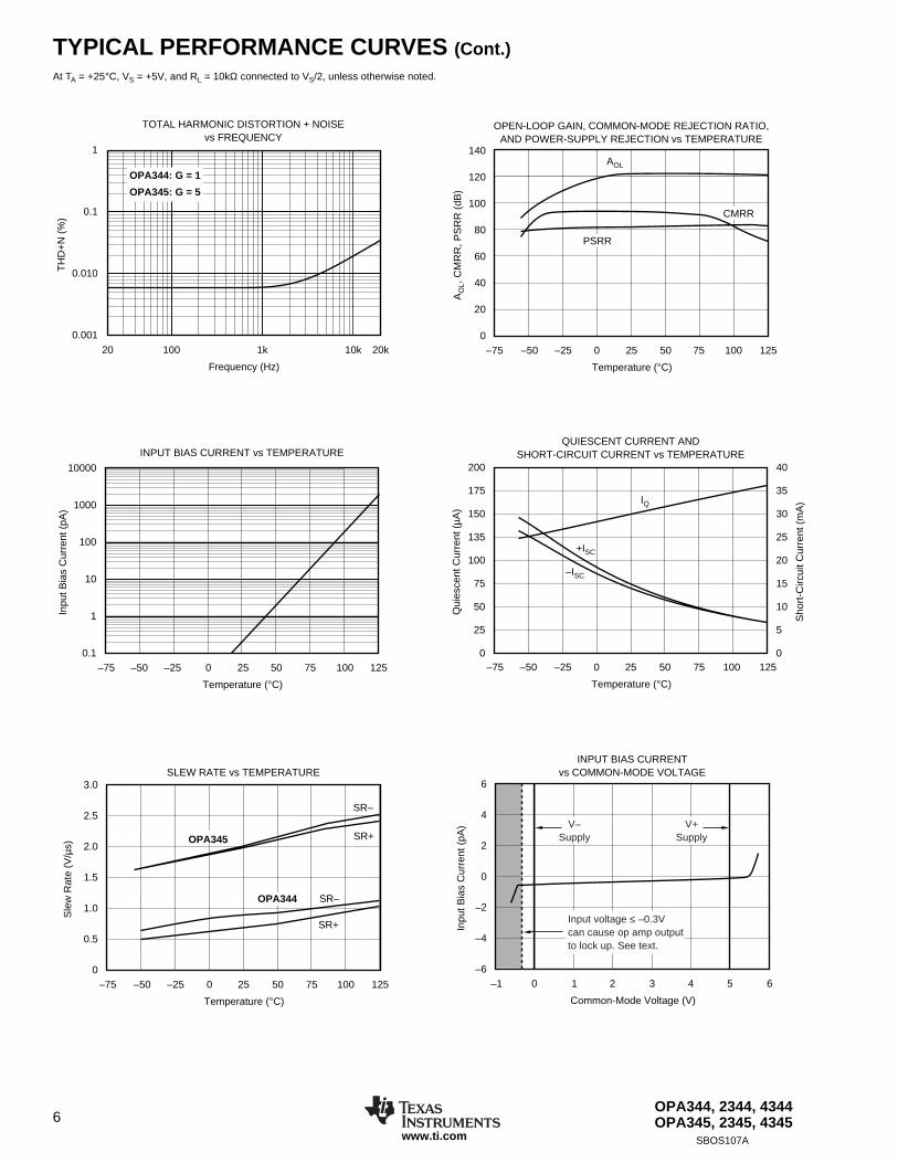
TYPICAL PERFORMANCE CURVES (Cont.)At TA = +25°C, VS = +5V, and RL = 10kΩ connected to VS/2, unless otherwise noted.
TOTAL HARMONIC DISTORTION + NOISEvs FREQUENCY
20
TH
D+
N (
%)
Frequency (Hz)
100 1k 10k 20k
1
0.1
0.010
0.001
OPA344: G = 1
OPA345: G = 5
OPEN-LOOP GAIN, COMMON-MODE REJECTION RATIO,AND POWER-SUPPLY REJECTION vs TEMPERATURE
AOL
–75
AO
L, C
MR
R, P
SR
R (
dB)
Temperature (°C)
–25 0 25–50 50 12575 100
140
120
100
80
60
40
20
0
CMRR
PSRR
INPUT BIAS CURRENT vs TEMPERATURE
–75
Inpu
t Bia
s C
urre
nt (
pA)
Temperature (°C)
–25 0 25–50 10050 75 125
10000
1000
100
10
1
0.1
QUIESCENT CURRENT ANDSHORT-CIRCUIT CURRENT vs TEMPERATURE
–75 –50 0
Qui
esce
nt C
urre
nt (
µA)
Temperature (°C)
25 50 100
IQ
+ISC
–ISC
75–25 125
200
175
150
135
100
75
50
25
0
Sho
rt-C
ircui
t Cur
rent
(m
A)
40
35
30
25
20
15
10
5
0
SLEW RATE vs TEMPERATURE
–75
Sle
w R
ate
(V/µ
s)
Temperature (°C)
250
SR–
SR–
SR+
SR+
7550–25–50 125100
3.0
2.5
2.0
1.5
1.0
0.5
0
OPA345
OPA344
INPUT BIAS CURRENTvs COMMON-MODE VOLTAGE
–1
Inpu
t Bia
s C
urre
nt (
pA)
Common-Mode Voltage (V)
0 1 2 43 5 6
6
4
2
0
–2
–4
–6
V+Supply
V–Supply
Input voltage ≤ –0.3Vcan cause op amp outputto lock up. See text.
www.ti.comSBOS107A
OPA344, 2344, 4344OPA345, 2345, 4345 7
TYPICAL PERFORMANCE CURVES (Cont.)At TA = +25°C, VS = +5V, and RL = 10kΩ connected to VS/2, unless otherwise noted.
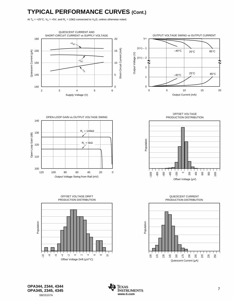
QUIESCENT CURRENT ANDSHORT-CIRCUIT CURRENT vs SUPPLY VOLTAGE
Qui
esce
nt C
urre
nt (
µA)
Supply Voltage (V)
2 3 4 5 6
+ISC
–ISC
IQ
160
155
150
145
140
Sho
rt-C
ircui
t Cur
rent
(m
A)
20
15
10
5
0
OPEN-LOOP GAIN vs OUTPUT VOLTAGE SWING140
130
120
110
100
Ope
n-Lo
op G
ain
(dB
)
Output Voltage Swing from Rail (mV)
120 100 80 60 40 20 0
RL = 5kΩ
RL = 100kΩ
OUTPUT VOLTAGE SWING vs OUTPUT CURRENT
0
Out
put V
olta
ge (
V)
Output Current (mA)
5
≈≈
10 15 20
V+
(V+) – 1
(V+) – 2
2
1
0
85°C25°C–40°C
85°C25°C–40°C
QUIESCENT CURRENTPRODUCTION DISTRIBUTION
Pop
ulat
ion
Quiescent Current (µA)
100
115
130
145
160
175
190
205
220
235
250
OFFSET VOLTAGEPRODUCTION DISTRIBUTION
Pop
ulat
ion
Offset Voltage (µV)
–10
00
–80
0
–60
0
–40
0
–20
0 0
200
400
600
800
100
0
OFFSET VOLTAGE DRIFTPRODUCTION DISTRIBUTION
Pop
ulat
ion
Offset Voltage Drift (µV/°C)
–10 –8 –6 –4 –2 0 2 4 6 8 10
www.ti.com
OPA344, 2344, 4344OPA345, 2345, 43458
SBOS107A
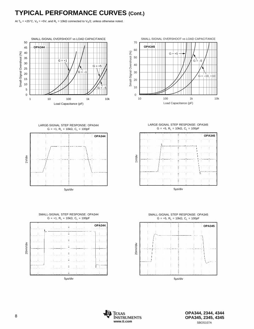
TYPICAL PERFORMANCE CURVES (Cont.)At TA = +25°C, VS = +5V, and RL = 10kΩ connected to VS/2, unless otherwise noted.
70
60
50
40
30
20
10
0
Sm
all-S
igna
l Ove
rsho
ot (
%)
SMALL-SIGNAL OVERSHOOT vs LOAD CAPACITANCE
100 1k 10k10
Load Capacitance (pF)
G = –5
G = –10, +10
G = +5
OPA345
20m
V/d
iv
5µs/div
SMALL-SIGNAL STEP RESPONSE: OPA345G = +5, RL = 10kΩ, CL = 100pF
OPA345
20m
V/d
iv
5µs/div
SMALL-SIGNAL STEP RESPONSE: OPA344G = +1, RL = 10kΩ, CL = 100pF
OPA344
5µs/div
LARGE-SIGNAL STEP RESPONSE: OPA344G = +1, RL = 10kΩ, CL = 100pF
1V/d
iv
OPA344
5µs/div
LARGE-SIGNAL STEP RESPONSE: OPA345G = +5, RL = 10kΩ, CL = 100pF
1V/d
ivOPA345
SMALL-SIGNAL OVERSHOOT vs LOAD CAPACITANCE
1
Sm
all-S
igna
l Ove
rsho
ot (
%)
Load Capacitance (pF)
10 100 1k 10k
G = –1
G = –5
50
45
40
35
30
25
20
15
10
5
0
OPA344
G = +5
G = +1
www.ti.comSBOS107A
OPA344, 2344, 4344OPA345, 2345, 4345 9
APPLICATIONS INFORMATIONOPA344 series op amps are unity gain stable and can operateon a single supply, making them highly versatile and easy touse. OPA345 series op amps are optimized for applicationsrequiring higher speeds with gains of 5 or greater.
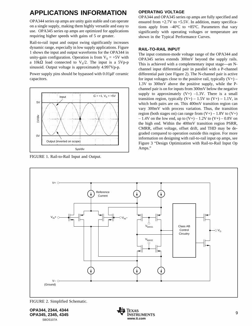
Rail-to-rail input and output swing significantly increasesdynamic range, especially in low supply applications. Figure1 shows the input and output waveforms for the OPA344 inunity-gain configuration. Operation is from VS = +5V witha 10kΩ load connected to VS/2. The input is a 5Vp-psinusoid. Output voltage is approximately 4.997Vp-p.
Power supply pins should be bypassed with 0.01µF ceramiccapacitors.
OPERATING VOLTAGEOPA344 and OPA345 series op amps are fully specified andensured from +2.7V to +5.5V. In addition, many specifica-tions apply from –40ºC to +85ºC. Parameters that varysignificantly with operating voltages or temperature areshown in the Typical Performance Curves.
RAIL-TO-RAIL INPUTThe input common-mode voltage range of the OPA344 andOPA345 series extends 300mV beyond the supply rails.This is achieved with a complementary input stage—an N-channel input differential pair in parallel with a P-channeldifferential pair (see Figure 2). The N-channel pair is activefor input voltages close to the positive rail, typically (V+) –1.3V to 300mV above the positive supply, while the P-channel pair is on for inputs from 300mV below the negativesupply to approximately (V+) –1.3V. There is a smalltransition region, typically (V+) – 1.5V to (V+) – 1.1V, inwhich both pairs are on. This 400mV transition region canvary 300mV with process variation. Thus, the transitionregion (both stages on) can range from (V+) – 1.8V to (V+)– 1.4V on the low end, up to (V+) – 1.2V to (V+) – 0.8V onthe high end. Within the 400mV transition region PSRR,CMRR, offset voltage, offset drift, and THD may be de-graded compared to operation outside this region. For moreinformation on designing with rail-to-rail input op amps, seeFigure 3 “Design Optimization with Rail-to-Rail Input OpAmps.”
FIGURE 2. Simplified Schematic.
VBIAS1
VBIAS2
VIN+ VIN–
Class ABControlCircuitry
VO
V–(Ground)
V+
ReferenceCurrent
FIGURE 1. Rail-to-Rail Input and Output.
5µs/div
1V/d
iv
Output (inverted on scope)
Input G = +1, VS = +5V
5V
0V

www.ti.com
OPA344, 2344, 4344OPA345, 2345, 434510
SBOS107A
COMMON-MODE REJECTIONThe CMRR for the OPA344 and OPA345 is specified inseveral ways so the best match for a given application maybe used. First, the CMRR of the device in the common-moderange below the transition region (VCM < (V+) – 1.8V) isgiven. This specification is the best indicator of the capabil-ity of the device when the application requires use of one ofthe differential input pairs. Second, the CMRR at VS = 5.5Vover the entire common-mode range is specified. Third, theCMRR at VS = 2.7V over the entire common-mode range isprovided. These last two values include the variations seenthrough the transition region.
INPUT VOLTAGE BEYOND THE RAILS
If the input voltage can go more than 0.3V below thenegative power supply rail (single-supply ground), specialprecautions are required. If the input voltage goes suffi-ciently negative, the op amp output may lock up in aninoperative state. A Schottky diode clamp circuit will pre-vent this—see Figure 4. The series resistor prevents exces-sive current (greater than 10mA) in the Schottky diode andin the internal ESD protection diode, if the input voltage canexceed the positive supply voltage. If the signal source islimited to less than 10mA, the input resistor is not required.
RAIL-TO-RAIL OUTPUTA class AB output stage with common-source transistors isused to achieve rail-to-rail output. This output stage iscapable of driving 600Ω loads connected to any potential
between V+ and ground. For light resistive loads (> 50kΩ),the output voltage can typically swing to within 1mV fromsupply rail. With moderate resistive loads (2kΩ to 50kΩ),the output can swing to within a few tens of millivolts fromthe supply rails while maintaining high open-loop gain. Seethe typical performance curve “Output Voltage Swing vsOutput Current.”
VO
VIN
VB
V+
Non-Inverting Gain
VCM = VIN
VO
VB
VIN
V+
Inverting Amplifier
VCM = VB
VO
VIN
V+
G = 1 Buffer
VCM = VIN = VO
FIGURE 3. Design Optimization with Rail-to-Rail Input Op Amps.
Rail-to-rail op amps can be used in virtually any op ampconfiguration. To achieve optimum performance, how-ever, applications using these special double-input-stageop amps may benefit from consideration of their specialbehavior.
In many applications, operation remains within the com-mon-mode range of only one differential input pair.However some applications exercise the amplifier throughthe transition region of both differential input stages.Although the two input stages are laser trimmed forexcellent matching, a small discontinuity may occur inthis transition. Careful selection of the circuit configura-tion, signal levels and biasing can often avoid this transi-tion region.
DESIGN OPTIMIZATION WITH RAIL-TO-RAIL INPUT OP AMPS
With a unity-gain buffer, for example, signals will traversethis transition at approximately 1.3V below V+ supplyand may exhibit a small discontinuity at this point.
The common-mode voltage of the non-inverting ampli-fier is equal to the input voltage. If the input signal alwaysremains less than the transition voltage, no discontinuitywill be created. The closed-loop gain of this configura-tion can still produce a rail-to-rail output.
Inverting amplifiers have a constant common-mode volt-age equal to VB. If this bias voltage is constant, nodiscontinuity will be created. The bias voltage can gener-ally be chosen to avoid the transition region.
FIGURE 4. Input Current Protection for Voltages Exceed-
ing the Supply Voltage.
1kΩ
OPA34410mA max
V+
VIN
VOUT
IOVERLOAD
IN5818
Schottky diode is required only if input voltage can go more than 0.3V below ground.
CAPACITIVE LOAD AND STABILITYThe OPA344 in a unity-gain configuration and the OPA345in gains greater than 5 can directly drive up to 250pF purecapacitive load. Increasing the gain enhances the amplifier’sability to drive greater capacitive loads. See the typical
www.ti.comSBOS107A
OPA344, 2344, 4344OPA345, 2345, 4345 11
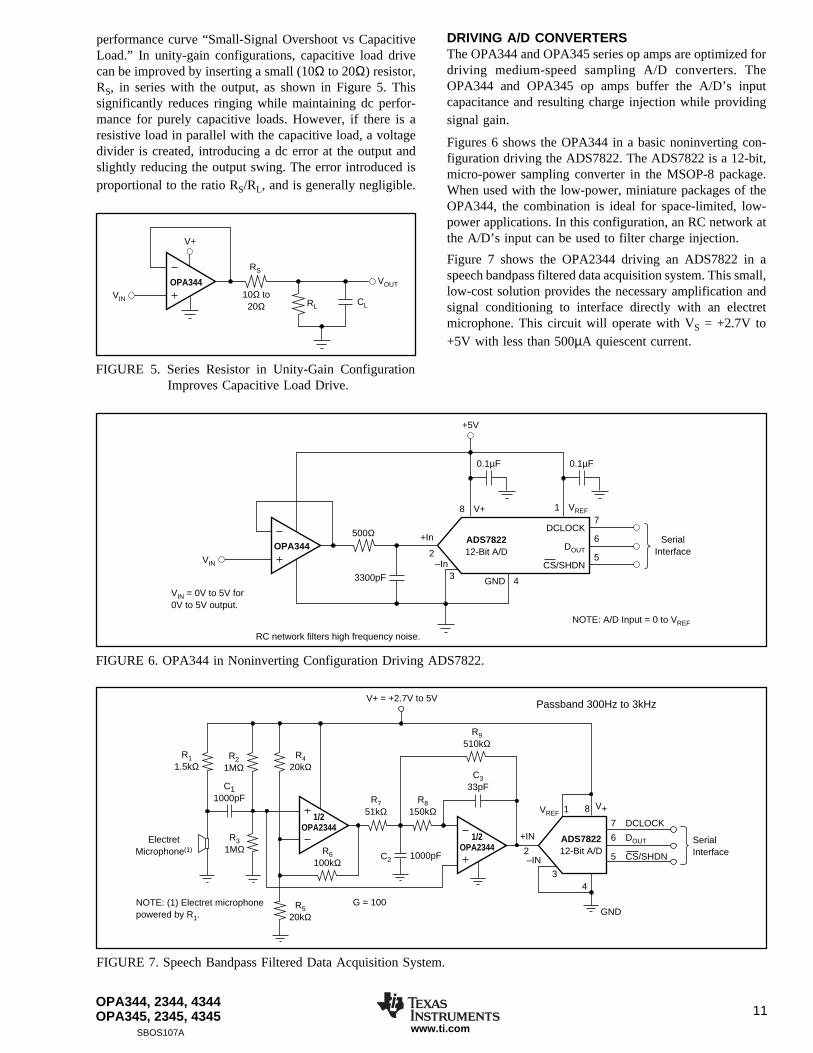
performance curve “Small-Signal Overshoot vs CapacitiveLoad.” In unity-gain configurations, capacitive load drivecan be improved by inserting a small (10Ω to 20Ω) resistor,RS, in series with the output, as shown in Figure 5. Thissignificantly reduces ringing while maintaining dc perfor-mance for purely capacitive loads. However, if there is aresistive load in parallel with the capacitive load, a voltagedivider is created, introducing a dc error at the output andslightly reducing the output swing. The error introduced isproportional to the ratio RS/RL, and is generally negligible.
FIGURE 6. OPA344 in Noninverting Configuration Driving ADS7822.
FIGURE 7. Speech Bandpass Filtered Data Acquisition System.
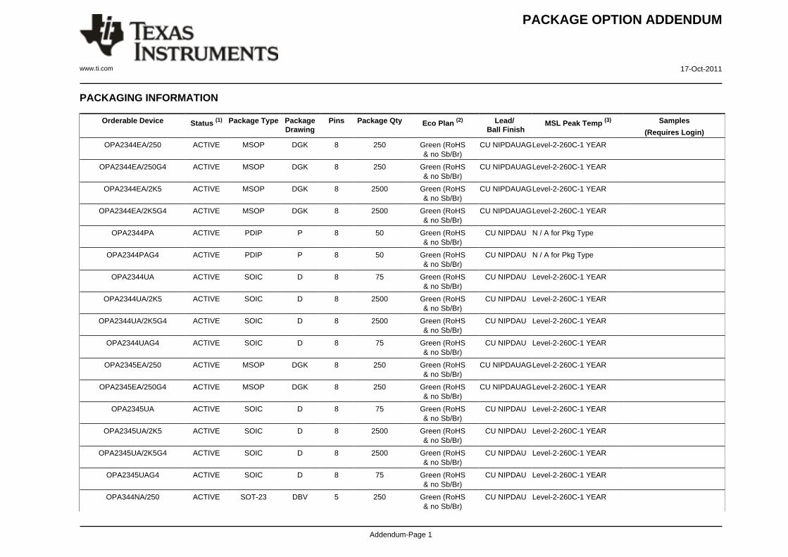
DRIVING A/D CONVERTERSThe OPA344 and OPA345 series op amps are optimized fordriving medium-speed sampling A/D converters. TheOPA344 and OPA345 op amps buffer the A/D’s inputcapacitance and resulting charge injection while providingsignal gain.
Figures 6 shows the OPA344 in a basic noninverting con-figuration driving the ADS7822. The ADS7822 is a 12-bit,micro-power sampling converter in the MSOP-8 package.When used with the low-power, miniature packages of theOPA344, the combination is ideal for space-limited, low-power applications. In this configuration, an RC network atthe A/D’s input can be used to filter charge injection.
Figure 7 shows the OPA2344 driving an ADS7822 in aspeech bandpass filtered data acquisition system. This small,low-cost solution provides the necessary amplification andsignal conditioning to interface directly with an electretmicrophone. This circuit will operate with VS = +2.7V to+5V with less than 500µA quiescent current.
FIGURE 5. Series Resistor in Unity-Gain ConfigurationImproves Capacitive Load Drive.
10Ω to20Ω
OPA344
V+
VIN
VOUT
RS
RLCL
C333pF
V+
GND
3
1 8
4
5
6
7
–IN
+IN
2C2
DCLOCK
Serial Interface1000pF
R11.5kΩ
R420kΩ
R520kΩ
R6100kΩ
R8150kΩ
R9510kΩ
R751kΩ
DOUT
VREF
V+ = +2.7V to 5V
CS/SHDN
C11000pF
ElectretMicrophone(1)
G = 100
Passband 300Hz to 3kHz
R31MΩ
R21MΩ
NOTE: (1) Electret microphonepowered by R1.
ADS782212-Bit A/D
1/2OPA2344
1/2OPA2344
ADS782212-Bit A/D
DCLOCK
DOUT
CS/SHDN
OPA344
+5V
VIN
V+
2
+In
3–In
VREF8
4GND
SerialInterface
1
0.1µF 0.1µF
7
6
5
NOTE: A/D Input = 0 to VREF
VIN = 0V to 5V for0V to 5V output.
RC network filters high frequency noise.
500Ω
3300pF
PACKAGE OPTION ADDENDUM
www.ti.com 17-Oct-2011
Addendum-Page 1
PACKAGING INFORMATION
Orderable Device Status (1) Package Type PackageDrawing
Pins Package Qty Eco Plan (2) Lead/Ball Finish
MSL Peak Temp (3) Samples
(Requires Login)
OPA2344EA/250 ACTIVE MSOP DGK 8 250 Green (RoHS& no Sb/Br)
CU NIPDAUAGLevel-2-260C-1 YEAR
OPA2344EA/250G4 ACTIVE MSOP DGK 8 250 Green (RoHS& no Sb/Br)
CU NIPDAUAGLevel-2-260C-1 YEAR
OPA2344EA/2K5 ACTIVE MSOP DGK 8 2500 Green (RoHS& no Sb/Br)
CU NIPDAUAGLevel-2-260C-1 YEAR
OPA2344EA/2K5G4 ACTIVE MSOP DGK 8 2500 Green (RoHS& no Sb/Br)
CU NIPDAUAGLevel-2-260C-1 YEAR
OPA2344PA ACTIVE PDIP P 8 50 Green (RoHS& no Sb/Br)
CU NIPDAU N / A for Pkg Type
OPA2344PAG4 ACTIVE PDIP P 8 50 Green (RoHS& no Sb/Br)
CU NIPDAU N / A for Pkg Type
OPA2344UA ACTIVE SOIC D 8 75 Green (RoHS& no Sb/Br)
CU NIPDAU Level-2-260C-1 YEAR
OPA2344UA/2K5 ACTIVE SOIC D 8 2500 Green (RoHS& no Sb/Br)
CU NIPDAU Level-2-260C-1 YEAR
OPA2344UA/2K5G4 ACTIVE SOIC D 8 2500 Green (RoHS& no Sb/Br)
CU NIPDAU Level-2-260C-1 YEAR
OPA2344UAG4 ACTIVE SOIC D 8 75 Green (RoHS& no Sb/Br)
CU NIPDAU Level-2-260C-1 YEAR
OPA2345EA/250 ACTIVE MSOP DGK 8 250 Green (RoHS& no Sb/Br)
CU NIPDAUAGLevel-2-260C-1 YEAR
OPA2345EA/250G4 ACTIVE MSOP DGK 8 250 Green (RoHS& no Sb/Br)
CU NIPDAUAGLevel-2-260C-1 YEAR
OPA2345UA ACTIVE SOIC D 8 75 Green (RoHS& no Sb/Br)
CU NIPDAU Level-2-260C-1 YEAR
OPA2345UA/2K5 ACTIVE SOIC D 8 2500 Green (RoHS& no Sb/Br)
CU NIPDAU Level-2-260C-1 YEAR
OPA2345UA/2K5G4 ACTIVE SOIC D 8 2500 Green (RoHS& no Sb/Br)
CU NIPDAU Level-2-260C-1 YEAR
OPA2345UAG4 ACTIVE SOIC D 8 75 Green (RoHS& no Sb/Br)
CU NIPDAU Level-2-260C-1 YEAR
OPA344NA/250 ACTIVE SOT-23 DBV 5 250 Green (RoHS& no Sb/Br)
CU NIPDAU Level-2-260C-1 YEAR

PACKAGE OPTION ADDENDUM
www.ti.com 17-Oct-2011
Addendum-Page 2
Orderable Device Status (1) Package Type PackageDrawing
Pins Package Qty Eco Plan (2) Lead/Ball Finish
MSL Peak Temp (3) Samples
(Requires Login)
OPA344NA/250G4 ACTIVE SOT-23 DBV 5 250 Green (RoHS& no Sb/Br)
CU NIPDAU Level-2-260C-1 YEAR
OPA344NA/3K ACTIVE SOT-23 DBV 5 3000 Green (RoHS& no Sb/Br)
CU NIPDAU Level-2-260C-1 YEAR
OPA344NA/3KG4 ACTIVE SOT-23 DBV 5 3000 Green (RoHS& no Sb/Br)
CU NIPDAU Level-2-260C-1 YEAR
OPA344PA ACTIVE PDIP P 8 50 Green (RoHS& no Sb/Br)
CU NIPDAU N / A for Pkg Type
OPA344PAG4 ACTIVE PDIP P 8 50 Green (RoHS& no Sb/Br)
CU NIPDAU N / A for Pkg Type
OPA344UA ACTIVE SOIC D 8 75 Green (RoHS& no Sb/Br)
CU NIPDAU Level-2-260C-1 YEAR
OPA344UA/2K5 ACTIVE SOIC D 8 2500 Green (RoHS& no Sb/Br)
CU NIPDAU Level-2-260C-1 YEAR
OPA344UA/2K5G4 ACTIVE SOIC D 8 2500 Green (RoHS& no Sb/Br)
CU NIPDAU Level-2-260C-1 YEAR
OPA344UAG4 ACTIVE SOIC D 8 75 Green (RoHS& no Sb/Br)
CU NIPDAU Level-2-260C-1 YEAR
OPA345NA/250 ACTIVE SOT-23 DBV 5 250 Green (RoHS& no Sb/Br)
CU NIPDAU Level-2-260C-1 YEAR
OPA345NA/250G4 ACTIVE SOT-23 DBV 5 250 Green (RoHS& no Sb/Br)
CU NIPDAU Level-2-260C-1 YEAR
OPA345UA ACTIVE SOIC D 8 75 Green (RoHS& no Sb/Br)
CU NIPDAU Level-2-260C-1 YEAR
OPA345UAG4 ACTIVE SOIC D 8 75 Green (RoHS& no Sb/Br)
CU NIPDAU Level-2-260C-1 YEAR
OPA4344EA/250 ACTIVE TSSOP PW 14 250 Green (RoHS& no Sb/Br)
CU NIPDAU Level-1-260C-UNLIM
OPA4344EA/250G4 ACTIVE TSSOP PW 14 250 Green (RoHS& no Sb/Br)
CU NIPDAU Level-1-260C-UNLIM
OPA4344EA/2K5 ACTIVE TSSOP PW 14 2500 Green (RoHS& no Sb/Br)
CU NIPDAU Level-1-260C-UNLIM
OPA4344EA/2K5G4 ACTIVE TSSOP PW 14 2500 Green (RoHS& no Sb/Br)
CU NIPDAU Level-1-260C-UNLIM
OPA4344PA ACTIVE PDIP N 14 25 Green (RoHS& no Sb/Br)
CU NIPDAU N / A for Pkg Type
PACKAGE OPTION ADDENDUM
www.ti.com 17-Oct-2011
Addendum-Page 3
Orderable Device Status (1) Package Type PackageDrawing
Pins Package Qty Eco Plan (2) Lead/Ball Finish
MSL Peak Temp (3) Samples
(Requires Login)
OPA4344PAG4 ACTIVE PDIP N 14 25 Green (RoHS& no Sb/Br)
CU NIPDAU N / A for Pkg Type
OPA4344UA ACTIVE SOIC D 14 50 Green (RoHS& no Sb/Br)
CU NIPDAU Level-2-260C-1 YEAR
OPA4344UA/2K5 ACTIVE SOIC D 14 2500 Green (RoHS& no Sb/Br)
CU NIPDAU Level-2-260C-1 YEAR
OPA4344UA/2K5G4 ACTIVE SOIC D 14 2500 Green (RoHS& no Sb/Br)
CU NIPDAU Level-2-260C-1 YEAR
OPA4344UAG4 ACTIVE SOIC D 14 50 Green (RoHS& no Sb/Br)
CU NIPDAU Level-2-260C-1 YEAR
OPA4345EA/250 ACTIVE TSSOP PW 14 250 Green (RoHS& no Sb/Br)
CU NIPDAU Level-2-260C-1 YEAR
OPA4345EA/250G4 ACTIVE TSSOP PW 14 250 Green (RoHS& no Sb/Br)
CU NIPDAU Level-2-260C-1 YEAR
OPA4345UA ACTIVE SOIC D 14 50 Green (RoHS& no Sb/Br)
CU NIPDAU Level-2-260C-1 YEAR
OPA4345UAG4 ACTIVE SOIC D 14 50 Green (RoHS& no Sb/Br)
CU NIPDAU Level-2-260C-1 YEAR
(1) The marketing status values are defined as follows:ACTIVE: Product device recommended for new designs.LIFEBUY: TI has announced that the device will be discontinued, and a lifetime-buy period is in effect.NRND: Not recommended for new designs. Device is in production to support existing customers, but TI does not recommend using this part in a new design.PREVIEW: Device has been announced but is not in production. Samples may or may not be available.OBSOLETE: TI has discontinued the production of the device.
(2) Eco Plan - The planned eco-friendly classification: Pb-Free (RoHS), Pb-Free (RoHS Exempt), or Green (RoHS & no Sb/Br) - please check http://www.ti.com/productcontent for the latest availabilityinformation and additional product content details.TBD: The Pb-Free/Green conversion plan has not been defined.Pb-Free (RoHS): TI's terms "Lead-Free" or "Pb-Free" mean semiconductor products that are compatible with the current RoHS requirements for all 6 substances, including the requirement thatlead not exceed 0.1% by weight in homogeneous materials. Where designed to be soldered at high temperatures, TI Pb-Free products are suitable for use in specified lead-free processes.Pb-Free (RoHS Exempt): This component has a RoHS exemption for either 1) lead-based flip-chip solder bumps used between the die and package, or 2) lead-based die adhesive used betweenthe die and leadframe. The component is otherwise considered Pb-Free (RoHS compatible) as defined above.Green (RoHS & no Sb/Br): TI defines "Green" to mean Pb-Free (RoHS compatible), and free of Bromine (Br) and Antimony (Sb) based flame retardants (Br or Sb do not exceed 0.1% by weightin homogeneous material)
(3) MSL, Peak Temp. -- The Moisture Sensitivity Level rating according to the JEDEC industry standard classifications, and peak solder temperature.
PACKAGE OPTION ADDENDUM
www.ti.com 17-Oct-2011
Addendum-Page 4
Important Information and Disclaimer:The information provided on this page represents TI's knowledge and belief as of the date that it is provided. TI bases its knowledge and belief on informationprovided by third parties, and makes no representation or warranty as to the accuracy of such information. Efforts are underway to better integrate information from third parties. TI has taken andcontinues to take reasonable steps to provide representative and accurate information but may not have conducted destructive testing or chemical analysis on incoming materials and chemicals.TI and TI suppliers consider certain information to be proprietary, and thus CAS numbers and other limited information may not be available for release.
In no event shall TI's liability arising out of such information exceed the total purchase price of the TI part(s) at issue in this document sold by TI to Customer on an annual basis.
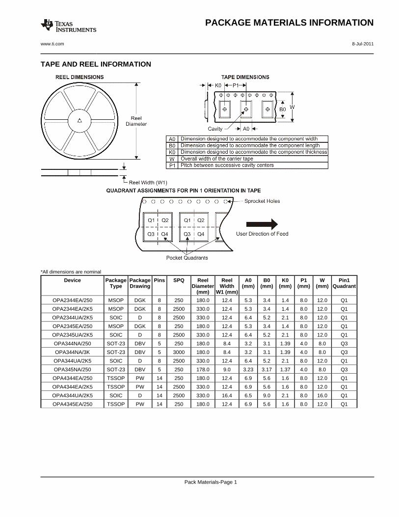
TAPE AND REEL INFORMATION
*All dimensions are nominal
Device PackageType
PackageDrawing
Pins SPQ ReelDiameter
(mm)
ReelWidth
W1 (mm)
A0(mm)
B0(mm)
K0(mm)
P1(mm)
W(mm)
Pin1Quadrant
OPA2344EA/250 MSOP DGK 8 250 180.0 12.4 5.3 3.4 1.4 8.0 12.0 Q1
OPA2344EA/2K5 MSOP DGK 8 2500 330.0 12.4 5.3 3.4 1.4 8.0 12.0 Q1
OPA2344UA/2K5 SOIC D 8 2500 330.0 12.4 6.4 5.2 2.1 8.0 12.0 Q1
OPA2345EA/250 MSOP DGK 8 250 180.0 12.4 5.3 3.4 1.4 8.0 12.0 Q1
OPA2345UA/2K5 SOIC D 8 2500 330.0 12.4 6.4 5.2 2.1 8.0 12.0 Q1
OPA344NA/250 SOT-23 DBV 5 250 180.0 8.4 3.2 3.1 1.39 4.0 8.0 Q3
OPA344NA/3K SOT-23 DBV 5 3000 180.0 8.4 3.2 3.1 1.39 4.0 8.0 Q3
OPA344UA/2K5 SOIC D 8 2500 330.0 12.4 6.4 5.2 2.1 8.0 12.0 Q1
OPA345NA/250 SOT-23 DBV 5 250 178.0 9.0 3.23 3.17 1.37 4.0 8.0 Q3
OPA4344EA/250 TSSOP PW 14 250 180.0 12.4 6.9 5.6 1.6 8.0 12.0 Q1
OPA4344EA/2K5 TSSOP PW 14 2500 330.0 12.4 6.9 5.6 1.6 8.0 12.0 Q1
OPA4344UA/2K5 SOIC D 14 2500 330.0 16.4 6.5 9.0 2.1 8.0 16.0 Q1
OPA4345EA/250 TSSOP PW 14 250 180.0 12.4 6.9 5.6 1.6 8.0 12.0 Q1
PACKAGE MATERIALS INFORMATION
www.ti.com 8-Jul-2011
Pack Materials-Page 1
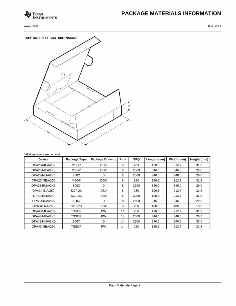
*All dimensions are nominal
Device Package Type Package Drawing Pins SPQ Length (mm) Width (mm) Height (mm)
OPA2344EA/250 MSOP DGK 8 250 190.5 212.7 31.8
OPA2344EA/2K5 MSOP DGK 8 2500 346.0 346.0 29.0
OPA2344UA/2K5 SOIC D 8 2500 346.0 346.0 29.0
OPA2345EA/250 MSOP DGK 8 250 190.5 212.7 31.8
OPA2345UA/2K5 SOIC D 8 2500 346.0 346.0 29.0
OPA344NA/250 SOT-23 DBV 5 250 190.5 212.7 31.8
OPA344NA/3K SOT-23 DBV 5 3000 190.5 212.7 31.8
OPA344UA/2K5 SOIC D 8 2500 346.0 346.0 29.0
OPA345NA/250 SOT-23 DBV 5 250 180.0 180.0 18.0
OPA4344EA/250 TSSOP PW 14 250 190.5 212.7 31.8
OPA4344EA/2K5 TSSOP PW 14 2500 346.0 346.0 29.0
OPA4344UA/2K5 SOIC D 14 2500 346.0 346.0 33.0
OPA4345EA/250 TSSOP PW 14 250 190.5 212.7 31.8
PACKAGE MATERIALS INFORMATION
www.ti.com 8-Jul-2011
Pack Materials-Page 2

IMPORTANT NOTICE
Texas Instruments Incorporated and its subsidiaries (TI) reserve the right to make corrections, modifications, enhancements, improvements,and other changes to its products and services at any time and to discontinue any product or service without notice. Customers shouldobtain the latest relevant information before placing orders and should verify that such information is current and complete. All products aresold subject to TI’s terms and conditions of sale supplied at the time of order acknowledgment.
TI warrants performance of its hardware products to the specifications applicable at the time of sale in accordance with TI’s standardwarranty. Testing and other quality control techniques are used to the extent TI deems necessary to support this warranty. Except wheremandated by government requirements, testing of all parameters of each product is not necessarily performed.
TI assumes no liability for applications assistance or customer product design. Customers are responsible for their products andapplications using TI components. To minimize the risks associated with customer products and applications, customers should provideadequate design and operating safeguards.
TI does not warrant or represent that any license, either express or implied, is granted under any TI patent right, copyright, mask work right,or other TI intellectual property right relating to any combination, machine, or process in which TI products or services are used. Informationpublished by TI regarding third-party products or services does not constitute a license from TI to use such products or services or awarranty or endorsement thereof. Use of such information may require a license from a third party under the patents or other intellectualproperty of the third party, or a license from TI under the patents or other intellectual property of TI.
Reproduction of TI information in TI data books or data sheets is permissible only if reproduction is without alteration and is accompaniedby all associated warranties, conditions, limitations, and notices. Reproduction of this information with alteration is an unfair and deceptivebusiness practice. TI is not responsible or liable for such altered documentation. Information of third parties may be subject to additionalrestrictions.
Resale of TI products or services with statements different from or beyond the parameters stated by TI for that product or service voids allexpress and any implied warranties for the associated TI product or service and is an unfair and deceptive business practice. TI is notresponsible or liable for any such statements.
TI products are not authorized for use in safety-critical applications (such as life support) where a failure of the TI product would reasonablybe expected to cause severe personal injury or death, unless officers of the parties have executed an agreement specifically governingsuch use. Buyers represent that they have all necessary expertise in the safety and regulatory ramifications of their applications, andacknowledge and agree that they are solely responsible for all legal, regulatory and safety-related requirements concerning their productsand any use of TI products in such safety-critical applications, notwithstanding any applications-related information or support that may beprovided by TI. Further, Buyers must fully indemnify TI and its representatives against any damages arising out of the use of TI products insuch safety-critical applications.
TI products are neither designed nor intended for use in military/aerospace applications or environments unless the TI products arespecifically designated by TI as military-grade or "enhanced plastic." Only products designated by TI as military-grade meet militaryspecifications. Buyers acknowledge and agree that any such use of TI products which TI has not designated as military-grade is solely atthe Buyer's risk, and that they are solely responsible for compliance with all legal and regulatory requirements in connection with such use.
TI products are neither designed nor intended for use in automotive applications or environments unless the specific TI products aredesignated by TI as compliant with ISO/TS 16949 requirements. Buyers acknowledge and agree that, if they use any non-designatedproducts in automotive applications, TI will not be responsible for any failure to meet such requirements.
Following are URLs where you can obtain information on other Texas Instruments products and application solutions:
Products Applications
Audio www.ti.com/audio Communications and Telecom www.ti.com/communications
Amplifiers amplifier.ti.com Computers and Peripherals www.ti.com/computers
Data Converters dataconverter.ti.com Consumer Electronics www.ti.com/consumer-apps
DLP® Products www.dlp.com Energy and Lighting www.ti.com/energy
DSP dsp.ti.com Industrial www.ti.com/industrial
Clocks and Timers www.ti.com/clocks Medical www.ti.com/medical
Interface interface.ti.com Security www.ti.com/security
Logic logic.ti.com Space, Avionics and Defense www.ti.com/space-avionics-defense
Power Mgmt power.ti.com Transportation and Automotive www.ti.com/automotive
Microcontrollers microcontroller.ti.com Video and Imaging www.ti.com/video
RFID www.ti-rfid.com
OMAP Mobile Processors www.ti.com/omap
Wireless Connectivity www.ti.com/wirelessconnectivity
TI E2E Community Home Page e2e.ti.com
Mailing Address: Texas Instruments, Post Office Box 655303, Dallas, Texas 75265Copyright © 2011, Texas Instruments Incorporated