Embed Size (px)
Citation preview

LINEARIZATION TECHNIQUES FOR INTEGRATED CMOS POWER AMPLIFIERS AND A HIGH EFFICIENCY CLASS-F GaN POWER AMPLIFIER
By
SANGWON KO
A DISSERTATION PRESENTED TO THE GRADUATE SCHOOL OF THE UNIVERSITY OF FLORIDA IN PARTIAL FULFILLMENT
OF THE REQUIREMENTS FOR THE DEGREE OF DOCTOR OF PHILOSOPHY
UNIVERSITY OF FLORIDA
2007
1

© 2007 Sangwon Ko
2

To my parents
3

ACKNOWLEDGMENTS
I would like to thank the chair of my committee members, Professor Jenshan Lin. He
guided and supported me during my Ph.D program. I also appreciate the other committee
members, Professor William R. Eisenstadt, Professor Bashirullah, and Professor Fan Ren for
their interest in this work and expert assistance.
Specially, I would like to express my appreciation to Professor William R. Eisenstadt for
his guidance and support. I am also grateful to Professor Fan Ren for his encouragement.
Finally, I cannot express how grateful I am to my parents for their unceasing love and
dedication. Most importantly, I thank God for caring for me throughout my life.
4

TABLE OF CONTENTS page
ACKNOWLEDGMENTS ...............................................................................................................4
LIST OF TABLES...........................................................................................................................8
LIST OF FIGURES .........................................................................................................................9
ABSTRACT...................................................................................................................................13
CHAPTER
1 INTRODUCTION ..................................................................................................................15
1.1 Motivation and Research Objective..................................................................................15
1.1.1 High Linearity Power Amplifier ............................................................................15
1.1.2 Power Amplifier using CMOS Process..................................................................16
1.1.3 High Efficiency Power Amplifier using Wide Bandgap Device............................18
1.2 Organization .....................................................................................................................21
2 OVERVIEW OF APPLICATIONS AND THEORY OF POWER AMPLIFER...................23
2.1 Applications of Mobile Wireless Communications..........................................................23
2.1.1 Wireless Local Area Networks (WLANs) .............................................................23
2.1.2 Bluetooth ................................................................................................................24
2.1.3 Wireless Mobile Phones .........................................................................................25
2.2 Transmitter and RF Power Amplifier ...............................................................................26
2.3 Transmitter Topologies.....................................................................................................27
2.3.1 Direct Digital Synthesis Transmitter ......................................................................28
2.3.2 Direct Conversion Transmitter ...............................................................................29
2.3.3 Heterodyne Transmitter..........................................................................................30
2.4 Power Amplifier Performance Parameters .......................................................................31
2.4.1 1 dB Gain Compression Point ................................................................................31
2.4.2 Third Order Intercept Point (IIP3)..........................................................................33
2.4.3 Overall IIP3 of Cascaded Nonlinear Stages ...........................................................36
2.4.4 Intermodulation Distortion and Adjacent Channel Power Ratio............................39
2.4.5 Drain Efficiency and Power Added Efficiency ......................................................40
3 LINEARIZATION TECHNIQUES FOR POWER AMPLIFIERS .......................................42
3.1 Background of Linearization Techniques.........................................................................42
3.2 Power Back-off .................................................................................................................43
3.3 Feedback ...........................................................................................................................43
3.3.1 Direct Feedback......................................................................................................44
3.3.2 Envelope Elimination and Restoration Transmitter with Feedback.......................45
3.3.3 Polar Transmitter with Feedback............................................................................46
5

3.3.4 Cartesian Feedback.................................................................................................48
3.4 Predistortion......................................................................................................................51
3.4.1 Analog Type Predistorter .......................................................................................53
3.4.2 Digital Type Predistorter ........................................................................................55
3.5 Feedforward......................................................................................................................56
4 PREDISTORTER USING DIODE-CONNECTED MOSFET..............................................58
4.1 Background.......................................................................................................................58
4.2 Basic Configuration of the Predistorter ............................................................................58
4.3 Voltage and Current Swing through FET and Equivalent Elements ................................59
4.4 Large Signal S21 of the Predistorter.................................................................................62
4.5 Phase Characteristic of the Predistorter ............................................................................63
4.6 CMOS Power Amplifier with the Predistorter .................................................................65
4.7 Experimental Results ........................................................................................................67
5 LINEARIZATION OF CASCODE CMOS POWER AMPLIFIER ......................................74
5.1 Background.......................................................................................................................74
5.2 Control of Phase Characteristic of the Predistorter ..........................................................75
5.3 Cascode CMOS Power Amplifier with the Predistorter...................................................77
5.4 Linearization Performance................................................................................................78
5.5 Experimental Results ........................................................................................................80
6 PREDISTORTER USING MOSFET IN NEAR-COLD FET CONDITION ........................86
6.1 Background.......................................................................................................................86
6.2 Basic Configuration of the Predistorter ............................................................................87
6.3 Voltage and Current Swing through FET and Equivalent Elements ................................88
6.4 Large Signal S21 of the Predistorter.................................................................................91
6.5 Phase Characteristic of the Predistorter ............................................................................92
6.6 CMOS Power Amplifier with the Predistorter .................................................................93
6.7 Experimental Results ........................................................................................................96
7 COMPARISON AMONG PREDISTORTERS AND STATE OF ART CMOS PREDISTORTERS...............................................................................................................101
7.1 Comparison between Developed Predistorters...............................................................101
7.1.1 Comparison between Predistorter using the Diode-Connected MOSFET and Predistorter using the Schottky Diode. ......................................................................101
7.1.2 Comparison between Predistorter using MOSFET in Near-Cold FET Condition and Predistorter using the Diode-Connected MOSFET............................101
7.2 Integrated RF and IF Predistorters..................................................................................102
7.2.1 State of Art IF Predistorter ...................................................................................102
7.2.2 State of Art RF Predistorter ..................................................................................102
7.2.3 Bias Stabilization using Active Bias Circuit ........................................................103
8 HIGH EFFICIENCY POWER AMPLIFIERS.....................................................................105
6

8.1 Background.....................................................................................................................105
8.2 Class A and Class B Power Amplifier............................................................................106
8.3 Class C Power Amplifier ................................................................................................108
8.4 Class D Power Amplifier................................................................................................109
8.5 Class E Power Amplifier ................................................................................................110
8.6 Class F Power Amplifier ................................................................................................113
9 A HIGH EFFICIENCY CLASS-F POWER AMPLIFIER USING A GA-N DEVICE ......117
9.1 Background.....................................................................................................................117
9.2 Modeling of GaN Device................................................................................................117
9.3 Design of Class-F Power Amplifier ...............................................................................120
9.4 Fabrication and Measurement.........................................................................................124
10 SUMMARY AND FUTURE WORK ..................................................................................128
10.1 Summary and Conclusion.............................................................................................128
10.1.1 Summary on Linearization of CMOS Power Amplifier.....................................128
10.1.2 Summary on High Efficiency GaN Power Amplifier ........................................130
10.2 Implication for Future Work.........................................................................................131
10.2.1 Implication for Future Work on Linearization of CMOS Power Amplifier ......131
10.2.2 Implication for Future Work on High Efficiency GaN Power Amplifier ..........131
LIST OF REFERENCES.............................................................................................................133
BIOGRAPHICAL SKETCH .......................................................................................................140
7

LIST OF TABLES
Table page 1-1 Characteristics comparison of technologies. ..........................................................................18
1-2 Properties of Si, GaAs, SiC, and GaN....................................................................................20
2-1 Properties of popular 802.11 standards ..................................................................................24
2-2 Classes of Bluetooth standards ...............................................................................................25
5-1 Input and output scattering parameters...................................................................................84
8-1 Classification of amplifiers...................................................................................................109
10-1 Measurement results of fabricated power amplifiers. ........................................................129
10-2 Integrated RF and IF linearization circuits. ........................................................................130
8

LIST OF FIGURES
Figure page 2-1 Configuration of a transmitter. ..............................................................................................27
2-2 A direct digital synthesis transmitter. ....................................................................................28
2-3 A direct conversion transmitter. ............................................................................................29
2-4 A heterodyne transmitter. ......................................................................................................30
2-5 Gain compression of a power amplifier. ...............................................................................32
2-6 Output spectrum of a power amplifier with two tone input signal. .......................................33
2-7 Third order intercept point of a power amplifier. ..................................................................34
2-8 Cascade of three nonlinear blocks. ........................................................................................36
3-1 Multi-channel approach with several single channel power amplifiers. ...............................42
3-2 Feedback system applied to an amplifier. .............................................................................44
3-3 Series feedback and parallel feedback...................................................................................45
3-4 An envelope feedback system ...............................................................................................46
3-5 A polar feedback system........................................................................................................47
3-6 A modulated signal on Cartesian coordinates. ......................................................................49
3-7 A Cartesian feedback.............................................................................................................50
3-8 Gain characteristics of a power amplifier with a predistorter. ..............................................51
3-9 A cubic type RF predistorter. ................................................................................................54
3-10 A simple type RF predistorter. ............................................................................................55
3-11 Feedforward system.............................................................................................................56
4-1 Basic configuration of predistorter. .......................................................................................59
4-2 Dynamic impedance line of predistorter. ..............................................................................59
4-3 Voltage and current waveforms of predistorter. ....................................................................60
4-4 Impedance of predistorter on Smith chart. ............................................................................60
9

4-5 Equivalent RV and CV of predistorter. ...................................................................................61
4-6 Gain and phase of the predistorter. ........................................................................................63
4-7 Predistorter with an additional parallel capacitor. .................................................................64
4-8 Phase variation of predistorter for four different values of CP. .............................................64
4-9 CMOS power amplifier with predistorter..............................................................................65
4-10 Relative gain and phase of the power amplifier. .................................................................66
4-11 IMD3 characteristic of the power amplifier. .......................................................................66
4-12 Power amplifier with predistorter........................................................................................67
4-13 Measured scattering parameters. .........................................................................................68
4-14 Measured output power, gain, and PAE. .............................................................................68
4-15 Two tone measurement setup. .............................................................................................69
4-16 Arrangement of measurement equipments. .........................................................................70
4-17 Measured IMD3 characteristic with low bias voltage for the predistorter. .........................71
4-18 Simulated IMD3 characteristic with low bias voltage for the predistorter..........................71
4-19 Measured IMD3 characteristic of the high bias voltage for the predistorter.......................72
4-20 Simulated IMD3 characteristic of the high bias voltage for the predistorter. .....................72
5-1 Gain and phase characteristics of cascode power amplifier with predistorter. .....................74
5-2 Predistorter having positive AM-PM characteristic. .............................................................75
5-3 Gain and phase of the predistorter with parallel inductor. ....................................................76
5-4 S21 of the predistorter. ..........................................................................................................77
5-5 Schematic diagram of the power amplifier............................................................................78
5-6 Relative gain and phase of the power amplifier. ....................................................................79
5-7 IMD3 characteristic of the power amplifier. ..........................................................................79
5-8 Power amplifier with predistorter..........................................................................................80
5-9 Measured scattering parameters. ...........................................................................................81
10

5-10 Measured output power, gain, and PAE. .............................................................................82
5-11 Measured IMD3 characteristic with low bias voltage for the predistorter. .........................82
5-12 Simulated IMD3 characteristic with low bias voltage for the predistorter..........................83
5-13 Measured IMD3 characteristic with high bias voltage for the predistorter. .........................83
5-14 Simulated IMD3 characteristic with high bias voltage for the predistorter. ........................84
6-1 Basic configuration of predistorter. .......................................................................................87
6-2 Impedance variation of predistorter with 0 V drain to source voltage. .................................88
6-3 Dynamic impedance line of predistorter. ..............................................................................89
6-4 Voltage and current waveforms of predistorter. ....................................................................89
6-5 Equivalent RV and CV of predistorter. ...................................................................................90
6-6 Gain and phase of predistorter...............................................................................................91
6-7 Predistorter with an additional parallel capacitor. .................................................................92
6-8 Phase variation of predistorter for four different sizes of CP.................................................93
6-9 CMOS power amplifier with predistorter..............................................................................94
6-10 Relative gain and phase of the power amplifier. .................................................................95
6-11 IMD3 characteristic of the power amplifier. .......................................................................95
6-12 Power amplifier with predistorter........................................................................................96
6-13 Measured scattering parameters. .........................................................................................97
6-14 Measured output power, gain, and PAE. .............................................................................97
6-15 Measured IMD3 characteristic. ............................................................................................98
6-16 Simulated IMD3 characteristic. ............................................................................................98
8-1 A single-ended RF power amplifier. ...................................................................................106
8-2 Road-lines of class A, class B, class AB, and class C amplifier. ........................................107
8-3 A class D amplifier. .............................................................................................................110
8-4 A class E amplifier. .............................................................................................................111
11

8-5 A class F amplifier...............................................................................................................114
8-6 Voltage and current waveform at the output of the transistor of the class F amplifier. ......115
8-7 Voltage and current waveform at the output of the transistor of the inverse class F amplifier. ..........................................................................................................................116
9-1 AlGaN/GaN HEMT from Air Force. ..................................................................................118
9-2 S11 and S22. ........................................................................................................................119
9-3 S21 on polar coordinate.......................................................................................................119
9-4 Meandered quarter wavelength microstrip line for drain bias.............................................121
9-5 S21 and S11 of the quarter wavelength microstrip line.......................................................122
9-6 Designed class-F power amplifier. ......................................................................................123
9-7 Current and voltage wave form at the drain of the class F power amplifier. ......................124
9-8 Equipment setup for the measurement of scattering parameters. ........................................125
9-9 Measured scattering parameters. .........................................................................................125
9-10 Measured output power, gain, and PAE of the class F power amplifier. ..........................126
9-11 Fabricated class F power amplifier....................................................................................127
12

Abstract of Dissertation Presented to the Graduate School of the University of Florida in Partial Fulfillment of the Requirements for the Degree of Doctor of Philosophy
LINEARIZATION TECHNIQUES FOR INTEGRATED CMOS POWER AMPLIFIERS AND A HIGH EFFICIENCY CLASS-F GaN POWER AMPLIFIER
By
Sangwon Ko
August 2007
Chair: Jenshan Lin Major: Electrical and Computer Engineering
My study was on linearization techniques for integrated CMOS power amplifiers and a high
efficiency GaN power amplifier. My study proposes two types of predistortion linearization
circuits compatible with CMOS processes. Dynamic impedance lines of the nonlinearity
generation circuits of the proposed predistorters were analyzed and the equivalent circuits of the
nonlinearity generation circuit were obtained from the large signal simulation. Characteristics of the
predistorter circuits were analyzed and compared. The phase distortion characteristic of the
cascode CMOS power amplifier was also investigated. The predistorter circuits were fully
integrated into CMOS power amplifiers. Three kinds of CMOS power amplifier were fabricated
and the small signal characteristics and the large signal characteristics of the CMOS power
amplifier were measured. Results showed that the third-order intermodulation distortion of the
power amplifier was improved by the integrated predistorters. The developed predistorters can be
applied to both the CMOS process and the compound semiconductor process. The predistorters
also have low loss and low power consumption characteristics.
My study also describes a high efficiency power amplifier using a wide bandgap GaN HEMT
device. The dc and ac characteristics of GaN HEMT device were measured and modeled using the
Curtice cubic model. The GaN HEMT device was mounted on a high dielectric constant substrate and
13

class F configuration was implemented at the output of the GaN HEMT device. Results showed high efficiency operation of the power amplifier using a wide bandgap GaN device at microwave frequency. 14

CHAPTER 1 INTRODUCTION
1.1 Motivation and Research Objective
1.1.1 High Linearity Power Amplifier
Over the last few years, numerous wireless local area networks (WLANs) and mobile
phone networks have been established throughout the world and the number of WLAN users and
mobile phone subscriber has sky-rocketed. In order to realize the multimedia communication
service, the data transfer rate should be increased and thus spectrum efficient modulation
schemes needs to be employed. An ideal power amplifier is a linear device and amplifies a signal
without distortion. However, a real power amplifier is linear only within a limited power range
and inevitably suffers from gain distortion as well as phase distortion as the output power of the
power amplifier increases. The distortion due to nonlinearity of the power amplifier generates
output signals at harmonic frequencies and inter-modulated frequencies. The power products
from the third order intermodulation locate near the fundamental frequency and can not be
suppressed by a band pass filter.
The adoption of the spectrum efficient modulation scheme leads to the stringent linearity
specification for the power amplifier in the transmitter. In order to satisfy the stringent linearity
specification, the power amplifier is operated far from the saturation region and this leads to very
low efficiency of the transmitter because the power amplifier is the most power consuming
device of the whole transmitter system. For the wireless communication system, the low
efficiency of the power amplifier means the decrease of the operation time or the use of the
bulky battery. Hence, several linearization techniques have been developed for the power
amplifiers. However, it is known that the linearization circuit generally requires the tuning
process and it is difficult to realize the linearization circuit as an integrated form.
15

The first part of this dissertation is concerned with the development of the linearization
circuit suitable for the integration using the cost-effective CMOS process. The linearization
techniques include the feedforward, feedback, and predistortion. Among three linearization
techniques, the feedforward technique provides the best linearity performance. In general, the
feedforward technique is used for the base station power amplifier, because it has large size and
low efficiency. The feedback technique has been successfully employed for the analog amplifiers.
Differently from the feedforward technique, the feedback technique automatically corrects the
process variation, temperature fluctuations, and aging [1]. Several feedback techniques have
been investigated for the RF power amplifier. The feedback loop can be added to the envelope
elimination and restoration (EER) system [2]-[4] and polar transmitter [5]-[7]. In the case of
Cartesian feedback, the feedback is the basic operation mechanism of the circuit. Although it is
known that the Cartesian feedback technique is appropriate for narrow-band application, several
researches have been conducted to increase the bandwidth of feedback system. In recent study,
the Cartesian feedback transmitter was investigated for the TETRA standard [8] and EDGE
standard [9].
For the integration purpose which is the goal of this dissertation, the RF predistortion
technique is the most promising among several linearization techniques. Currently, several
integrated RF type predistorter were reported but it is still challenge to integrate the predistorter
circuit with the power amplifier. In this dissertation, two kinds of predistorter are proposed for a
CMOS process and the predistorters are fully integrated with the CMOS power amplifiers.
1.1.2 Power Amplifier using CMOS Process
The power amplifier using the CMOS process has drawbacks of low gain and low
efficiency compared to power amplifiers using other technologies. Despite these disadvantages,
the CMOS power amplifier has been intensively investigated because the developments of low
16

cost systems are inevitable for new short range wireless services to be introduced in the market.
As the feature size of MOSFET continues to scale down, the speed of MOSFET has become
applicable for RF applications. However, with the decreasing feature size of MOSFET, the
breakdown voltage of the MOSFET is reduced, and thus the available output power of the
CMOS amplifier also decreases.
For the implementation of fully integrated CMOS power amplifiers, the metal electro-
migration issue is the other limiting factor on the available output power [10]. If the current
density on the metal line is bigger than a specified metal migration threshold current density
(JMAX), the metal line starts to be damaged and eventually gets fused. The metal migration issue
requires the line width of the on-chip inductor of CMOS process to be excessively wide. The
inductor using a very wide metal line occupies a large chip area and has necessarily very low self
resonance frequencies [11]. In the case of 0.18 µm mixed-mode UMC process, the sixth metal
line of the line width from 1µm to 10 µm has JMAX of 1.74 mA/µm at 100°C and 0.89 mA/µm at
125°C respectively. The power amplifiers using CMOS technology are widely designed in 2.4
GHz band applications such as Bluetooth [12]-[13] and WLAN 802.11b[14].
Although the CMOS process has the possibility of one chip integration of the power
amplifier with a transmitter system, the fully integrated power amplifier necessarily goes through
the performance degradation in the gain, output power, linearity, efficiency, and thermal
dissipation. In the case of a mobile phone which requires a high performance power amplifier,
the power amplifier is not implemented as an integrated chip but a module which includes a
GaAs or InGaP power amplifier chip, off-chip output matching network, and a control circuit
chip.
17
The performance degradation of a chip power amplifier is serious especially in CMOS
processes. The on-chip inductor at the output matching network of the CMOS power amplifier
degrades the gain, efficiency, and output power. The main source of the loss of the on-chip
inductor is the conductive silicon substrate on the contrary to the case of the insulating GaAs
substrate. The fully integrated power amplifier in the CMOS process has been designed only for
low output power application such as Bluetooth or WLAN [15].
1.1.3 High Efficiency Power Amplifier using Wide Bandgap Device
Over the past decade, GaAs-based devices have been dominant devices for the power
amplifiers in wireless applications. A GaAs device has inherently higher operation speed due to
its improved electron mobility and saturated drift velocity [16]. A GaAs device also has superior
performance in gain and power added efficiency although it has a high cost and a low level of
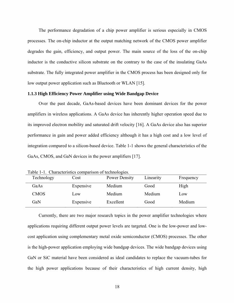
integration compared to a silicon-based device. Table 1-1 shows the general characteristics of the
GaAs, CMOS, and GaN devices in the power amplifiers [17].
Table 1-1. Characteristics comparison of technologies.
Technology Cost Power Density Linearity Frequency
GaAs Expensive Medium Good High
CMOS Low Medium Medium Low
GaN Expensive Excellent Good Medium
Currently, there are two major research topics in the power amplifier technologies where
applications requiring different output power levels are targeted. One is the low-power and low-
cost application using complementary metal oxide semiconductor (CMOS) processes. The other
is the high-power application employing wide bandgap devices. The wide bandgap devices using
GaN or SiC material have been considered as ideal candidates to replace the vacuum-tubes for
the high power applications because of their characteristics of high current density, high
18
breakdown voltage, and high temperature operation. The application areas of the high power
transmitter include the radar system in military vehicles, wireless power transmission, and space
exploration. Currently, vacuum-tubes are dominant devices for the microwave and millimeter-
wave transmitter applications in which the kilowatt to megawatt levels of power is delivered [18].
In the case of the GaAs devices, the sustainable dc voltage for the drain is low and thus a
large dc current is required to obtain high output power. A large area device is needed for the dc
large current and the large area device has inherently low operation frequency due to large
intrinsic capacitances at the input and output of the device [19]. Besides that, the large area
devices have low impedance at the output of the device and thus the impedance transformation
ratio at the output of the power amplifier is significant. In practice, the maximally possible
impedance transformation ratio of the output matching network of the power amplifier is a few
ohms.
In the case of a wide bandgap device, the high output power can be achieved with greatly
relieved impedance transformation ratio of the output matching network because high supply
voltage can be applied to the drain of the device [20]. While the GaAs devices have the
breakdown field of slightly over 105 V/cm and the gate-drain breakdown voltage of 10 to12 volt,
both the GaN and the SiC devices have the breakdown fields greater than 106 V/cm and the drain
breakdown voltages of more than 50 volts [21]. High thermal conductivity is an extremely
important feature for high power application because the performance in this application depends
upon the ability to extract the heat generated from the dissipated power. The electronic barriers
of active devices become increasing leaky as the temperature increases and the operation
temperature of the conventional devices with the low electron barrier are limited accordingly.
The other advantage of a wide bandgap device is that the wide bandgap device can operate
19

reliably at high temperature greater than 250 °C [22]. Table 1-2 shows the properties of the wide
bandgap materials, SiC and GaN as well as the conventional materials, Si and GaAs.
Table 1-2. Properties of Si, GaAs, SiC, and GaN [23].
Material Energy gap (eV)
Thermal conductivity (W/cm-K)
Electron mobility (cm2/V-s)
Dielectric constant
Breakdown field (V/cm)
Si 1.12 1.3 1350 11.7 3 × 10⁵
GaAs 1.41 0.55 8500 12.9 4 × 10⁵
SiC 3.0 4.9 400 9.66 3-5 × 10⁶
GaN 3.39 1.3 1000 8.9 5 × 10⁶
SiC has superior capability to other materials in terms of the thermal dissipation. This is
the reason that SiC is an attractive material for the substrate of the wide bandgap devices. The
thermal conductivity of SiC is four and a half times higher than that of Si, while the thermal
conductivity of GaN is virtually equal to that of Si. GaN has higher electron mobility than SiC
and thus the GaN device has the fundamental advantage over SiC devices for higher frequency
band applications such as the X and the Ku band.
The second part of this dissertation is concerned with the development of the high
efficiency power amplifier using wide bandgap device. The efficiency characteristic is an
important specification for power amplifiers because these are the most power-consuming
circuits in the entire transmitter system. The efficiency characteristic is related with the reliability
issue of the power amplifier. For the wireless mobile system, the efficiency of the power
amplifier determines the operation time and battery size of the system. For the base station
system, the efficiency of power amplifier determines the electricity usage cost for the power
amplifier and the cooling system [24]. In this dissertation, a class F configuration is realized
20

using microstrip lines and lumped elements and the high efficiency operation of the GaN HEMT
based power amplifier is demonstrated.
1.2 Organization
I give an overview of the wireless communication applications and the basic theory of the
power amplifier. After the wireless communication applications are introduced in the first
section, the function of a power amplifier in a transmitter is discussed and several transmitter
topologies are addressed. The advantages and disadvantages of a direct digital synthesis
transmitter, a direct upconversion transmitter, and a heterodyne transmitter are discussed. I deal
with important parameters of the power amplifier. The 1 dB gain compression point, third order
intercept point, intermodulation distortion, adjacent channel power ratio, drain efficiency, and
power added efficiency are covered. The linearization techniques for power amplifiers are
covered. The power back-off, envelope feedback, RF feedback, polar feedback, Cartesian
feedback, feedforward, and predistortion techniques are discussed and compared. I present the
first type of an integrated CMOS predistorter which uses a MOSFET in near-cold FET condition.
The characteristics of the predistorter are analyzed and then the predistorter is fully integrated
with a CMOS power amplifier using 0.18 µm 1P6M mixed-mode process. The second type of
the integrated preditorter using a diode-connected MOSFET is present. The characteristics of the
predistorter are analyzed and performances of the CMOS power amplifier integrated with the
predistorter are discussed. The characteristics of the cascode power amplifier are discussed. The
phase characteristic of the predistorter using a diode-connected MOSFET is controlled using an
additional inductor element and the negative AM-PM characteristic of the cascade CMOS power
amplifier is compensated using the predistorter with the additional inductor. The characteristics
and performances of the predistorter developed in the thesis are compared. The state of art RF
predistorters and IF predistorters using CMOS processes are described. The classes of the high
21

efficiency mode power amplifiers are discussed. The configurations for the high efficiency
operation of the power amplifier are discussed and compared. The class AB, class B, class C,
class D, class E, class F, and inverse class F power amplifiers are covered and the linearity
characteristic of the switching mode power amplifier is discussed. The high efficiency class F
power amplifier using 0.75 µm GaN HEMT is illustrated. The output matching network for the
class F operation is explained and performances of the fabricated power amplifier are described.
Lastly, the summary of the dissertation and future work are presented.
22

CHAPTER 2 OVERVIEW OF APPLICATIONS AND THEORY OF POWER AMPLIFER
2.1 Applications of Mobile Wireless Communications
2.1.1 Wireless Local Area Networks (WLANs)
WLAN links two or more computers wirelessly using spread-spectrum technology. Today,
the majority of computers are released equipped with wireless LAN devices. The benefits of
wireless LANs include the ease of installation, the low cost of installation, and the expandability
of the network. At the end of the 1990s, the various versions of WLAN standards which are also
called Wi-Fi were developed for mobile computing devices such as laptops. The 802.11a,
802.11b, and 802.11g are popular standards among 802.11 families. The maximum data rate of
802.11a standard is 54 Mbit/s and the data rate is reduced to 48, 36, 24, 18, 12, 9, then 6 Mbit/s
according to the data transmission condition [25]. The 802.11a standard has three operation
frequencies at 5 GHz band and is therefore not affected by interference from the heavily used 2.4
GHz ISM band. However, this high operation frequency also has disadvantages. The high
frequency signal cannot penetrate as far as the low frequency signal and thus the device using
802.11a standard needs to be in the line of sight, requiring more access points. The 802.11b
standard was ratified in 1999 and the maximum data rate of 802.11b standard is 11 Mbit/s at the
indoor range of 30 m and it typically reduces to 1 Mbit/s at the outdoor range of 90 m. The third
standard, 802.11g was ratified in June 2003 and has the maximum data rate of 54 Mbit/s. The
802.11b and 802.11g standards use the crowded 2.40 GHz band and the signal at this frequency
band suffers from the interference incurred from microwave ovens, Bluetooth devices, and
cordless telephones using this ISM band. Table 2-1 summarizes the characteristics of the popular
802.11 standards.
23

Table 2-1. Properties of popular 802.11 standards [26]-[28].
Standard Release Date
Operation Frequency (GHz)
Maximum Data Rate (Mbit/s)
Indoor Range (meter)
Outdoor Range (meter)
802.11 legacy 1997 2.4-2.5 2 ~ 25 ~ 75
801.11a 1999 5.15-5.35 5.47-5.725 5.725-5.875
54 ~ 30 ~ 100
802.11b 1999 2.4-2.5 11 ~ 35 ~110
802.11g 2003 2.4-2.5 54 ~ 35 ~ 115 2.1.2 Bluetooth
Bluetooth, known as IEEE 802.15.1, is an industrial specification for a wireless personal
network and it could remove the traditional cable connection of a variety of applications. The
applications of the Bluetooth network include:
• Exchange of the information among personal devices such as telephones, modems, headsets, digital cameras, and video game consoles.
• Transfer of data between input and output devices of personal computers such as the mouse, keyboards, and printers.
• Transfer of data between test equipment, global positioning system (GPS) receivers, medical equipments, and traffic control devices.
• Connection to a higher level of network and the Internet. Bluetooth operates in the globally unlicensed ISM band of 2.45 GHz and the Bluetooth
specifications were formalized and licensed by the Bluetooth Special Interest Group initially
established by Ericsson, Sony Ericsson, IBM, Intel, Toshiba, and Nokia. The data rates of
Bluetooth versions 1.1 and 1.2 are 723.1 kbps and the data rate of Bluetooth version 2.0 specified
November 2004, has the data rate of 3.0 Mbps. Bluetooth system is classified by the output
power ranges of the system as shown in Table 2-2. Although Bluetooth standard has little
bandwidth and provides low speed of data transmission, short coverage range, and poor security
24

compared to WLAN, Bluetooth does not require high performance devices. Basically Bluetooth
systems consume low power and can be implemented using low cost devices.
Table 2-2. Classes of Bluetooth standards [29].
Class Maximum Permitted Power Approximate Range of Reach
Class 1 100 mW (20 dBm) ~ 100 (meter)
Class 2 2.5 mW (4 dBm) ~ 10 (meter)
Class 3 1 mw (0 dBm) ~ 1 (meter) 2.1.3 Wireless Mobile Phones
Due to convenient establishment and low deployment cost, mobile phone networks have
spread rapidly throughout the world since the 1980s. In 2005, the total number of mobile phone
subscribers in the world was estimated at 2.14 billion. In 2006, the mobile phone service area in
the world will cover about 80 percent of the six billion people in the globe. The evolution of the
mobile phone technology is expressed by generations. Fully automatic cellular networks were
first introduced in the 1980s. The system in the first generation was analog and voice
communication was the main concern of the service.
The system in the second generation was digital and frequently referred to as Personal
Communications Service (PCS) in the United States. The second generation technology can be
divided into time division multiple access (TDMA) based standards and code division multiple
access (CDMA) based standards depending on the multiplexing method. The main 2G standards
includes GSM (TDMA based system from Europe), D-AMPS (TDMA-based system used in the
Americas), IS-95 (CDMA-based system used in the Americas and parts of Asia), and PDC
(TDMA-based system used exclusively in Japan). Currently, the mobile phone generation is
evolving from the second generation to the third generation.
25

The third generation system supports voice data transmission as well as non-voice data
transmission such as downloading music files and exchanging e-mails. The third generation
network and systems are officially defined by the International Telecommunication Union (ITU)
as a part of the International Mobile Telecommunications (IMT-2000) initiative. Third
generation standards include EDGE, W-CDMA, CDMA2000, TD-CDMA, and DECT. Among
these standards, EDGE and CDMA2000 are often called 2.5G services because the data rates of
these are 144 kbps which are several times slower than the data rate for true 3G services. True
3G allows the transmission of 384kbps for mobile systems and 2Mbps for stationary systems
[30].
Fourth generation will operate on internet technology and combine existing wired as well
as wireless technologies such as GSM, WLAN, and Bluetooth [31]. Fourth generation will
support the data rate of 100 Mbps in mobile phone networks and 1Gbps in local WLAN
networks. As third and fourth generations allow the mobile phone to transfer digital data, it is
expected that the mobile phone family will compete with WLAN of 802 wireless IEEE standards.
2.2 Transmitter and RF Power Amplifier
The transmitter consists of a back end block and a front end block. The back end block of
the transmitter performs the modulation of the information and the front end block performs the
upconversion of the modulated signal to a carrier frequency (Figure 2-1). The front end of the
transmitter includes mixers, filters, oscillators, a drive amplifier, an RF power amplifier, and an
antenna. The digital to analog converter (DAC) transforms the digital signal to the analog signal
and a mixer conducts the upconversion of the baseband signal to RF signal using a local
oscillator (LO). In order to supply a stable and correct local oscillation frequency, a phase locked
loop (PLL) is needed with a voltage controlled oscillator (VCO). The transmit/receive (T/R)
switching network controls the signal path from the antenna to the transmitter and receiver.
26

UserEnd
Antenna
BackEnd
FrontEnd
User information
Unmodulatedwanted signal
Modulatedwanted signal
Figure 2-1. Configuration of a transmitter.
The function of the RF power amplifier is to increase the power level of an input signal
and deliver the boosted signal to an antenna. The power level of the signal from the power
amplifier should be sufficiently high so that the antenna can transmit the signal through the air
with an appropriate power. During the process of the signal amplification, harmonic components
and spurious noises are necessarily generated in the power amplifier and these parasitic signals
should be filtered out by low pass filters before reaching the antenna. The power amplifier is one
of the key components in the mobile wireless system because the power amplifier determines the
quality of the voice and data transmission and the operation time of the mobile system. Also, it is
generally accepted that the power amplifier is one of the blocks which is difficult to integrate.
The integration of the power amplifier leads to the performance degradation and makes the
thermal dissipation difficult [32].
2.3 Transmitter Topologies
A wireless communication system can be split into a transmitter and a receiver. While
interferers may be bigger than wanted signals in the receiver channel, the interferer does not exist
in the transmitter channel. On the other hand, the power level of the signal in the transmitter is
much less than the power level of the signal in the receiver. Therefore, the transmitter is much
27

less sensitive to parasitic signals than the receiver and the dynamic range requirement on the
transmitter is not considerable [33]. This section describes three kinds of transmitter topologies
which are direct digital synthesis transmitter, direct upconversion transmitter (homodyne
transmitter), and heterodyne transmitter.
2.3.1 Direct Digital Synthesis Transmitter
In the transmitter using direct digital synthesis, the signal is upconverted in the digital
domain and the modulated digital signals are converted to an analog signal at RF frequency
(Figure 2-2).
D/A
Modulation
I
Q
LPF Amp Mixer
LPF Amp
FrequencySynthesizer
90°
RFSwitch
PA
Receiver
Antenna
Figure 2-2. A direct digital synthesis transmitter.
First advantage of the direct digital synthesis transmitter is that the quadrature
upconversion is performed by an algorithm using a digital signal processor (DSP) and thus a
high level of I and Q matching can be easily achieved [34]. The second advantage of the direct
digital synthesis transmitter is that the integration level of the system is very high and the cost of
the system is low because most of the functions of the direct digital synthesis transmitter are
28

conducted in the digital domain. The challenge of the direct digital synthesis is that the DSP and
DAC should operate at RF carrier frequency. Currently, the DSP used for signal processing is
too slow to handle RF signal. In addition, both resolution and linearity requirements on DAC are
hard to be satisfied with current CMOS technology.
2.3.2 Direct Conversion Transmitter
The direct conversion transmitter directly upconverts the modulated baseband signal to a
carrier signal in the analog domain (Figure 2-3).
D/A
Modulation
I
Q
LPF Amp Mixer
LPF Amp
FrequencySynthesizer
90°
RFSwitch
PA
Receiver
Antenna
D/A
Figure 2-3. A direct conversion transmitter.
In the quadrature upconversion of the direct upconversion transmitter, the upper and lower
sideband of the wanted signal are mirrored each other and signal interferences do not occur [33].
Therefore, there is no need for an off-chip filter to suppress the mirror signal generated during
the upconversion. This feature leads to the better integration of the direct conversion transmitter
than the heterodyne transmitter.The direct conversion transmitter has disadvantages. Because the
29

power amplifier and local oscillator have the same frequency, some portion of the feedback
signal from the output signal of the power amplifier is easily coupled with the local oscillator. In
this process, the noisy output of the power amplifier easily corrupts the oscillator frequency. The
other drawback is the crosstalk of the signal from the local oscillator to the RF carrier signal at
the upconversion mixer. This crosstalk can not be suppressed by a bandpass filter and thus is
transmitted from the antenna.
2.3.3 Heterodyne Transmitter
The heterodyne transmitter is the classical type of the transmitter and also the most often
used one. In the heterodyne transmitter, the modulated digital signal is converted to an analog
signal at the baseband and the analog signal is upconverted to an intermediate frequency signal
using analog mixers (Figure 2-4).
D/AM
odulationLPF Mixer
LPF
FrequencySynthesizer
90°
RFSwitch
PA
Receiver
Antenna
D/A
HF FilterMixerIF Filter
Figure 2-4. A heterodyne transmitter.
In the heterodyne transmitter, the RF carrier frequency is far from the intermediate
frequency of the local oscillator and thus the local oscillator is not affected by the high power
30

carrier signal. An advantage of the heterodyne transmitter over the direct conversion transmitter
is that I and Q matching is superior since quadrature modulation is performed at low frequency.
However, the simple second upconversion mixing produces both the wanted signal band and the
unwanted sideband. After the second upconversion, the unwanted sideband needs to be
suppressed by filtering. The passive type and off-chip filters are used for the filtering because the
center frequency of the filter is very high.
2.4 Power Amplifier Performance Parameters
This section describes the performance parameters of the power amplifier. For linearity
specifications, 1 dB gain compression point, third order intercept point, two tone intermodulation
distortion, and adjacent power ratio are discussed and for efficiency specifications, drain
efficiency and power added efficiency are described.
2.4.1 1 dB Gain Compression Point
There are many nonlinearity sources in a transistor and those nonlinearities of the transistor
cause the gain of the power amplifier to be decreased as the input power increases. The output 1
dB gain compression point is defined as the output power level in which the power gain is
reduced by 1 dB compared to the linear gain of the power amplifier (Figure 2-5).
For a single tone input of VIN=V⋅cosωt, the output of a power amplifier is represented as
equation 2.1.
tVa
tVa
tVa
VaVa
ttVa
tVatVa
tVatVatVatVO
ωωω
ωωωω
ωωω
3cos4
2cos2
cos4
32
)3coscos3(4
)2cos1(2
cos
coscoscos)(
33
22
33
12
33
22
1
333
2221
⋅+
⋅+⎟⎟
⎠
⎞⎜⎜⎝
⎛ ⋅+⋅+
⋅=
+⋅
++⋅
+⋅=
⋅+⋅+⋅=
(2.1)
where coefficient a3 has a negative value and the gain at the fundamental frequency has the
compressive characteristic with the increasing input power [35].
31

Saturationregion
Linear region(small-signal gain)
1dB
Output P1B
Pin(dBm)
Pout(dBm)
Input P1B
Figure 2-5. Gain compression of a power amplifier.
The voltage level at the 1 dB gain compression point can be obtained by equating the
fundamental component plus the third order product to the fundamental component minus 1 dB
as described in equation 2.2.
11
13131
891.0log20122.1
log20
1log2043log20
aa
dBaVaa dBI
⋅⋅=⋅=
−⋅=+⋅
( )3
1
3
11 38.01891.0
34
aa
aa
V dBI =⋅−= (2.2)
As the output power reaches the 1 dB gain compression point, the power of the undesired
harmonic components become significant. In the receiver system, these harmonic components
function as blockers and desensitize the receiver system. In the transceiver system, the harmonic
components increase the power level in adjacent channels.
32
2.4.2 Third Order Intercept Point (IIP3)
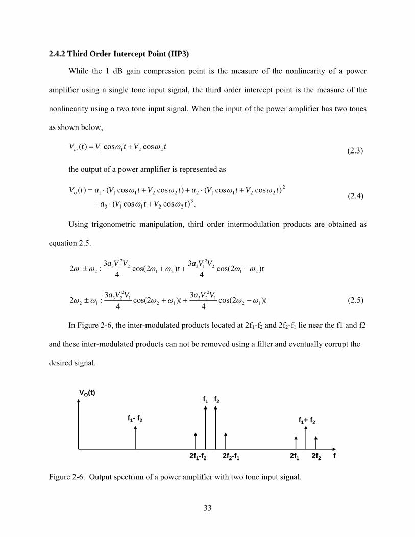
While the 1 dB gain compression point is the measure of the nonlinearity of a power
amplifier using a single tone input signal, the third order intercept point is the measure of the
nonlinearity using a two tone input signal. When the input of the power amplifier has two tones
as shown below,
tVtVtVin 2211 coscos)( ωω += (2.3)
the output of a power amplifier is represented as
.)coscos(
)coscos()coscos()(3
22113
22211222111
tVtVa
tVtVatVtVatVo
ωω
ωωωω
+⋅+
+⋅++⋅= (2.4)
Using trigonometric manipulation, third order intermodulation products are obtained as
equation 2.5.
tVVatVVa )2cos(4
3)2cos(4
3:2 212
213
212
213
21 ωωωωωω −++±
tVVa
tVVa
)2cos(4
3)2cos(
43
:2 121
223
121
223
12 ωωωωωω −++± (2.5)
In Figure 2-6, the inter-modulated products located at 2f1-f2 and 2f2-f1 lie near the f1 and f2
and these inter-modulated products can not be removed using a filter and eventually corrupt the
desired signal.
2f1-f2 2f2-f1 2f1 2f2
f1 f2
f1+ f2f1- f2
f
VO(t)
Figure 2-6. Output spectrum of a power amplifier with two tone input signal.
33
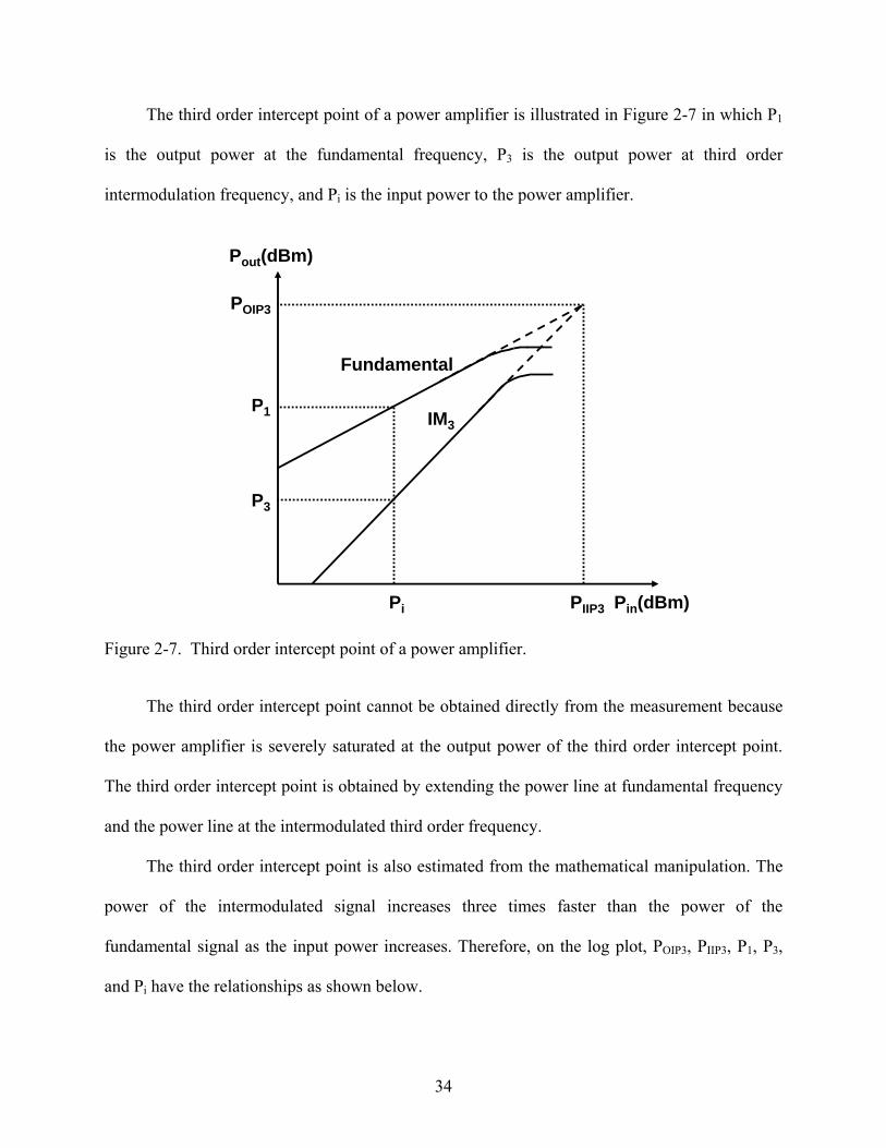
The third order intercept point of a power amplifier is illustrated in Figure 2-7 in which P1
is the output power at the fundamental frequency, P3 is the output power at third order
intermodulation frequency, and Pi is the input power to the power amplifier.
Pin(dBm)
Fundamental
IM3
POIP3
PIIP3Pi
P1
P3
Pout(dBm)
Figure 2-7. Third order intercept point of a power amplifier.
The third order intercept point cannot be obtained directly from the measurement because
the power amplifier is severely saturated at the output power of the third order intercept point.
The third order intercept point is obtained by extending the power line at fundamental frequency
and the power line at the intermodulated third order frequency.
The third order intercept point is also estimated from the mathematical manipulation. The
power of the intermodulated signal increases three times faster than the power of the
fundamental signal as the input power increases. Therefore, on the log plot, POIP3, PIIP3, P1, P3,
and Pi have the relationships as shown below.
34

1][][][][
3
13 =−−
dBmPdBmPdBmPdBmP
iIIP
OIP (2.6)
3][][][][
3
33 =−−
dBmPdBmPdBmPdBmP
iIIP
OIP (2.7)
where, 50
log10][2
33
IIPIIP
VdBmP ⋅= and
50log10][
23
3OIP
OIPV
dBmP ⋅= for the condition of 50 Ω
load.
The power amplifier has a power gain expressed by,
][][][][ 133 dBmPdBmPdBmPdBmPG iIIPOIP −=−= (2.8)
and equations 2.6 and 2.7 are solved to give
( )
( )][][21][
][][21][][
31
3113
dBmPdBmPdBmP
GdBmPdBmPdBmPdBmP
i
IIP
−⋅+=
−−⋅+= (2.9)
We can also relate the 1 dB gain compression point with the third order intercept point by
equating the fundamental component in equation 2.4 to the intermodulated third order
component in equation 2.5.
⎟⎠⎞
⎜⎝⎛ ⋅⋅=⋅⋅ 3
3331 43log20)log(20 IIPIIP VaVa
3
13 3
4aaVIIP ⋅= (2.10)
Using equation 2.2 and equation 2.10,
dBVV
VVPPdBI
IIPdBIIIPdBIIIP 6.9
1891.034
34
log20log20log20log201
31313 ≈
−==−=− (2.11)
35

Equation 2.11 shows that the power level at the third order intercept point is approximately
9.6 dB larger than the power level at the 1 dB gain compression point.
2.4.3 Overall IIP3 of Cascaded Nonlinear Stages
It is possible to estimate the overall third order intercept point of the multi-stage block in a
transmitter. The overall third order intercept point is approximately calculated using the third
order intercept point of the individual block.
VIIP3,1
a1, a2, a3
VIIP3,2 VIIP3,3
va(t) vb(t)b1, b2, b3 c1, c2, c3
vi(t) vc(t)
Figure 2-8. Cascade of three nonlinear blocks.
In Figure 2-8, the coefficients of the first, second, and the third block are denoted by a, b,
and c respectively and the input third order intercept voltage of the first, second, and the third
block are denoted by VIIP3,1, VIIP3,2, and VIIP3,3 respectively. The input voltage to the first stage,
the output voltage of the first stage, the output voltage of the second stage, the output voltage of
the third stages are denoted by vi(t), va(t), vb(t), vc(t) respectively. The behavior of each nonlinear
block is represented using polynomial coefficients by equations 2.12, 2.13, and 2.14.
)()()()( 3221 tvatvatvatv iiia ⋅+⋅+⋅= (2.12)
)()()()( 33
221 tvbtvbtvbtv aaab ⋅+⋅+⋅= , (2.13)
)()()()( 33
221 tvctvctvctv bbbc ⋅+⋅+⋅= , (2.14)
36

The output voltage of the second stage is obtained by substituting the input voltage of
equation 2.13 with the equation 2.12.
( )(( )33213
23212
3211
)()()(
)()()(
)()()()(
tvatvatvab
tvatvatvab
tvatvatvabtv
iii
iii
iiib
⋅+⋅+⋅⋅+
⋅+⋅+⋅⋅+ )⋅+⋅+⋅⋅=
(2.15)
Considering only the linear term and the third order term, equation 2.15 can be arranged as
⋅⋅⋅+⋅⋅+⋅⋅⋅+⋅+⋅⋅= 33
312211311 )2()()( iib vbabaabatvbatv . (2.16)
The coefficient of equation 2.16 can be applied to equation 2.10 to determine input third
order intercept voltage of the two cascaded block.
33122113
11
3
13 23
434
babaababa
aaVIIP ⋅+⋅⋅⋅+⋅
⋅⋅=⋅= . (2.17)
The signs of the coefficient of the denominator are circuit dependent. For the worst case,
the absolute values of the three terms in the denominator are added. After arranging equation
2.17, the overall input third order intercept voltage of the two cascaded blocks can be expressed
by the input third order intercept voltage of the individual block, VIIP3,1 and VIIP3,2, as shown in
equation 2.18.
22,3
21
1
222
1,3
1
321
1
22
1
3
11
33122113
23
231
43
23
43
2
431
IIPIIP
IIP
Va
bba
V
bb
ab
baaa
ba
babaaba
V
+⋅
⋅+=
⋅⋅+⋅
⋅+⋅=
⋅+⋅⋅⋅+⋅⋅=
(2.18)
The second order coefficients generate the second-order intermodulation components and
second order harmonics. In general, since each block in the cascaded RF system is a narrow band
circuit, the second order intermodulation components and the second order harmonics lie out of
37

the operation frequency band. Consequently, the second term in equation 2.18 becomes
negligible giving
22,3
21
21,3
23
11
IIPIIPIIP Va
VV+≈ . (2.19)
This equation can be expanded for the cascaded block with three stages.
⋅⋅⋅+⋅⋅
+⋅
++≈ 24,3
21
21
21
23,3
21
21
22,3
21
21,3
23
11
IIPIIPIIPIIPIIP Vcba
Vba
Va
VV (2.20)
Assuming that each block in Figure 2-8 is matched with a 50 Ω load to obtain maximum
power transfer, the power gain of each stage can be expressed in terms of the voltage gain of
each stage [36].
31
21
21
)'3(
)'2(
)'1(
cstagerdtheofgainPowerG
bstagendtheofgainPowerG
astagesttheofgainPowerG
c
b
a
=
=
=
(2.21)
Substituting the small signal gain with the power gain, the power relation equation can be
expressed as
⋅⋅⋅+⋅⋅
+⋅
++≈ 24,3
23,3
22,3
21,3
23
11
IIP
cba
IIP
ba
IIP
a
IIPIIP PGGG
PGG
PG
PP (2.21)
Although equation 2.21 is an approximated result, this equation can be expanded for the
cascaded block with more than the third stage. Since the power gain of each block is much larger
than unity and the third order intercept point of each stage is scaled down by the gain product of
all preceding stages, the overall third order intercept power of a cascaded block is dominated by
the third order intercept voltage of the last stage.
38

2.4.4 Intermodulation Distortion and Adjacent Channel Power Ratio
The two tone test is a universally accepted method of evaluating amplifier linearity and can
illustrate both the amplitude and the phase distortion characteristics of a power amplifier [37].
Two tone intermodulation distortion (IMD) is defined as the ratio of the power at third order
intermodulation frequency to the power at fundamental frequency.
When a multi-carrier input signal is applied to the power amplifier, the power at the
operation band spreads into the adjacent band due to the nonlinearities of the power amplifier.
The adjacent channel power ratio (ACPR) is defined as the ratio of the power at the operation
band to the power at adjacent band.
It is possible to approximate the multi-tone or complex signal behavior of a power
amplifier based on the simple two tone measurement as shown below [38].
⎟⎟⎠
⎞⎜⎜⎝
⎛+
⋅+−=BA
nIMDACPR dBcdBc 4log106
3
(2.22)
where 8
)2/mod(24
232 23 nnnnA +−−
= and ( )4
2/mod2 nnB −= ,
IMDdBc also denotes two tone intermodulation ratio and n is the number of tone.
For a random Gaussian excitation, the number of tone increases and equation 2.22 turns to
( ) dBcIMRACPRACPR dBcdBcndBc 25.4lim 2 −==∞→
. (2.23)
Although equation 2.23 provides an approximate result without detailed measurement, this
equation is based on several assumptions and has many sources of inaccuracy. One assumption is
that the power amplifier is memory-less and the characteristics of the power amplifier are
perfectly modeled by the Volterra-Weiner theories which state that any third order system may
be completely characterized by a three tone test. Another critical assumption is that the input
39
signal has a relatively narrow band spectrum composed of equally spaced tones with constant
amplitude.
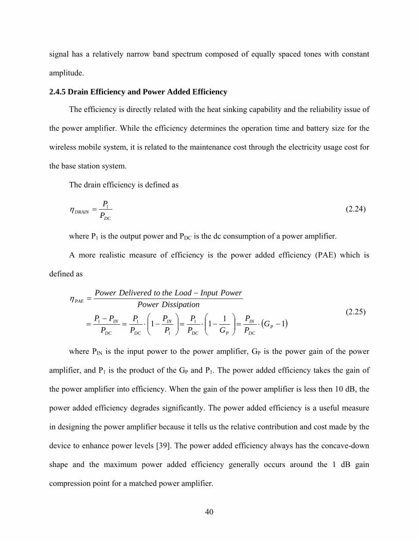
2.4.5 Drain Efficiency and Power Added Efficiency
The efficiency is directly related with the heat sinking capability and the reliability issue of
the power amplifier. While the efficiency determines the operation time and battery size for the
wireless mobile system, it is related to the maintenance cost through the electricity usage cost for
the base station system.
The drain efficiency is defined as
DCDRAIN P
P1=η (2.24)
where P1 is the output power and PDC is the dc consumption of a power amplifier.
A more realistic measure of efficiency is the power added efficiency (PAE) which is
defined as
( )1111 1
1
11 −⋅=⎟⎟⎠
⎞⎜⎜⎝
⎛−⋅=⎟⎟
⎠
⎞⎜⎜⎝
⎛−⋅=
−=
−=
PDC
IN
PDC
IN
DCDC
IN
PAE
GPP
GPP
PP
PP
PPP
nDissipatioPowerPowerInputLoadthetoDeliveredPowerη
(2.25)
where PIN is the input power to the power amplifier, GP is the power gain of the power
amplifier, and P1 is the product of the GP and P1. The power added efficiency takes the gain of
the power amplifier into efficiency. When the gain of the power amplifier is less then 10 dB, the
power added efficiency degrades significantly. The power added efficiency is a useful measure
in designing the power amplifier because it tells us the relative contribution and cost made by the
device to enhance power levels [39]. The power added efficiency always has the concave-down
shape and the maximum power added efficiency generally occurs around the 1 dB gain
compression point for a matched power amplifier.
40

41

CHAPTER 3 LINEARIZATION TECHNIQUES FOR POWER AMPLIFIERS
3.1 Background of Linearization Techniques
The linearity specification for a multi-channel application can be 30 or 40 dB higher than
the linearity specification for a single-channel application. Many systems designers still adopt a
channeling approach to satisfy the linearity specification for the power amplifier [24] (Figure 3-
1). In the channeling approach, the power amplifier for each channel has only moderate linearity
and the filtering is used to suppress the distortion components for each power amplifier.
Single Channel PAs
Multi-Channel Signal
Low Power Divider
High Power Combiner
Antenna
Figure 3-1. Multi-channel approach with several single channel power amplifiers.
The challenge of the channeling approach is the realization of the power divider and power
combiner that are normally implemented using the mechanical device of a traditional microwave
theory. If the cumbersome channeling approach is not used, some kinds of linearization
techniques should be applied for the power amplifier to satisfy the linearity specification. There
42

have been some efforts to apply the Volterra series theory [40] to improve the linearity of a
power amplifier linearization [41]. However, this analytic approach requires very heavy
calculation and leads to little insight. This chapter discusses the established linearization
techniques for power amplifiers. Power Back-off, RF feedback, polar loop, Cartesian loop,
feedforward, and predistortion techniques are covered.
3.2 Power Back-off
When a power amplifier is driven with decreased input power, the linearity of the power
amplifier is improved and the decreased amount in the output power level is called “back-off” of
the power amplifier. As an example, for a power amplifier having third order intermodulation
distortion of -20 dBc at the 1 dB output power compression point, a 10 dB of back-off of the
output power level leads to another 20 dBc drop in the third order intermodulation distortion.
However, this means that a 10 Watt transistor is used for 1 Watt output power and the efficiency
of the power amplifier is decreased to 10 % of the original efficiency at 1 dB compression point.
Therefore, the power back-off is not considered as a realistic method to improve the linearity of a
power amplifier.
3.3 Feedback
The feedback technique was developed by Block [42] and has been universally applied to
analog circuits since its invention. The closed loop gain of the feedback system (Figure 3-2) is
expressed as
)(1
)()(1)(
)()(
)(sFsFsA
sAsVsV
sAi
oCL ≈
⋅+== . (3.1)
where ACL(s) is the closed loop gain of the system, A(s) is the open loop gain of the
amplifier, and F(s) is a feedback factor.
43

ΣVi(S) Vo(S)
A(S)
F(S)
Figure 3-2. Feedback system applied to an amplifier.
For a operation amplifier of audio frequency, the open loop voltage gain of the amplifier is
typically in the range of 107 or 108 and thus the overall closed loop gain of the amplifier is
determined by the feedback factor F(s). In other words, the closed loop gain is desensitized from
any variation of the open loop gain A(s).
3.3.1 Direct Feedback
For a power amplifier at radio frequencies, it is not easy to apply the close loop feedback
technique because of two reasons. First, the phase delay through the closed feedback loop is
significant and the feedback loop may cause the instability. Second, the power gain of the RF
power amplifier is not high enough. Therefore, a simple type of direct feedback is used for the
RF power amplifier. The feedback network including both the series and the parallel feedback
resistor is shown in Figure 3-3. In the direct feedback, the feedback loop does not include the
gain stage. On the other hand, resistors for parallel feedback or series feedback are applied to the
active device itself. It is because the matching network causes the most of the delay of the RF
power amplifiers. As the Q factor of the matching network increases, the delay through the
matching network also increases.
44

Series Feedback
Parallel Feedback
RS
RP
InputMatchingNetwork
OutputMatchingNetwork
ActiveDevice
Figure 3-3. Series feedback and parallel feedback [15].
A series resistor used in series feedback causes the voltage drop across it and thus the gain
of the feedback system decreases due to the series feedback resistor. Because the gain of the RF
power amplifier is an important factor, the parallel feedback is more common configuration than
the series feedback for the RF power amplifier. When the feedback network is included in the RF
system, the stability characteristics of the system needs to be thoroughly checked using a
simulation tool.
3.3.2 Envelope Elimination and Restoration Transmitter with Feedback
The envelope elimination and restoration (EER) method proposed by L. Kahn in 1952 [43]
is one of ways to realize the high efficiency amplifier. The EER system is a transmitter systems
rather than single amplifier circuit. In the EER system, an envelope signal is separated from the
input signal using a directional coupler and an envelope detector at the input of the power
amplifier. The low frequency envelope signal is amplified by a high efficiency amplifier and
then applied as the supply voltage to the RF power amplifier. The envelope loop itself introduces
some amounts of envelope phase distortion (phase delay) during the detection and comparison
45

process. To prevent the phase distortion, the speed of analog circuits needs to be much faster
than the envelope modulation frequency. The phase signal is generated by clipping the input
signal with a limiter and then directly fed into the RF power amplifier.
To improve the linearity of the EER transmitter, a feedback loop can be applied to the EER
system (Figure 3-4). A portion of the output signal is sampled at the output of the power
amplifier using a directional coupler and the envelope signal is extracted using the envelope
detector. In [3], the EER transmitter with the envelop feedback was simulated with an orthogonal
frequency division multiplex (OFDM) signal. The effect of the phase feedback to the EER
transmitter was simulated in [4]. In [2], the L-band EER transmitter with the envelop feedback
was demonstrated.
PA
Switching Mode Amplifier
Atten.
CouplerCoupler
EnvelopDetector
EnvelopDetector LPF
Limiter
Figure 3-4. An envelope feedback system [4].
3.3.3 Polar Transmitter with Feedback
The polar feedback consists of two feedback loops which are a phase feedback loop and
amplitude (envelope) feedback loop. In the EER system, the envelope signal and phase signal are
46

obtained by sampling and processing a RF signal. Differently from it, in the polar transmitter, the
envelop signal and phase signal are generated directly from a digital signal processor [44]. The
polar feedback and Cartesian feedback are called in-direct feedback because the RF signal at the
output of the power amplifier is downconverted to IF signal and the feedback loop is closed at IF.
The mixer and synthesizer are used fro the downconversion of the RF signal. The
downconverted IF signal is divided into phase information and amplitude information (polar
form). A limiter is used to extract the phase signal from the IF signal using another IF signal
generated from an independent phase locked loop. A differential amplifier compares the detected
amplitude with a similarly detected input signal and the resulting error signal is fed back to the
power amplifier. The gain of feedback loops forces the error signal to be zero. The phase
feedback loop is a kind of phase locked loop and so the phase of the output signal is compared
with the phase of the input signal and the resulting error signal controls the VCO.
IF PLL
PA
LPFLPF
PhaseComp.
Diff-AmpLoop Amp RF
Synthesizer
VCO
LimiterLimiter
Atten.
Coupler
Figure 3-5. A polar feedback system [45].
47

As the feedback loop can be added to the EER system, it can be applied to the polar
transmitter to improve the linearity performance (Figure 3-5). The bandwidth limitation of the
error amplifier and analog circuits limit the performance of the polar loop feedback.
In [5], only envelop feedback was applied to the polar transmitter and the phase feed back
was not included. Therefore, this architecture does not correct AM-PM distortion and any
residual AM-PM distortion degraded the linearity performance. In [6]-[7], both of the envelope
and phase feedback were applied to correct AM-AM and AM-PM distortion of the power
amplifier. The systems of [5]-[7] were developed to meet the specifications of EDGE standard.
3.3.4 Cartesian Feedback
The modulated base band signal in a digital communication system can be described as
( )tfj cetgtv π2)(Re)( ⋅= (3.2)
where fc is the RF carrier frequency and g(t) is the complex envelope of the modulated
signal v(t) [46]. The complex envelope can be described in I and Q format (Cartesian
coordinates).
tjetAtQjtItg θ⋅=⋅+= )()()()( (3.3)
Here, I(t) is called in-phase signal and Q(t) is quadrature signal.
Using the Cartesian presentation of g(t), the modulated signal can be expressed in
Cartesian format as
( )( )
))(2cos()()2sin()()2cos()(
)()(Re)( 2
ttftAtftQtftI
etQjtItv
c
cc
tfj c
θπππ
π
+⋅=⋅−⋅=
⋅⋅+= (3.4)
where )(cos)()( ttAtI φ⋅= and )(sin)()( ttAtQ φ⋅= . A(t) has the information of the
amplitude modulation and θ(t) has the information of the phase modulation.
48

The envelope g(t) of the modulated signal is illustrated in Cartesian coordinates, I(t) and
Q(t) (Figure 3-6).
Q(t)
I(t)
Im
Re
A(t)
g(t)
θ(t)
Figure 3-6. A modulated signal on Cartesian coordinates.
While two objects of control in polar feedback are the amplitude and the phase, two
objects of control in Cartesian feedback are Cartesian components, I(t) and Q(t). In Cartesian
feedback, two identical feedback loops operate completely independently (Figure 3-7). A small
portion of the distorted RF signal is sampled by a directional coupler at the output of the power
amplifier and attenuated. The distorted RF signal is split into distorted Cartesian components, I(t)
and Q(t), by demodulator network. The distorted I(t) and Q(t) signal from the demodulator and
the undistorted I(t) and Q(t) signal from the input are fed into differential amplifiers. The
differential amplifiers compare two input signals and the amplified error signals are upconverted
to an RF signal using the modulator network. The gain of the differential amplifiers force the
output I(t) and Q(t) signal to closely track the input I (t) and Q(t) signals. The feedback technique
of the polar feedback and Cartesian feedback has an important advantage over a predistortion
technique. Because the feedback technique takes the output of the power amplifier as a reference
49

during the correction process, the feedback technique can overcome the behavior variation of the
power amplifier due to environmental variation, temperature variation, and memory effect.
PA90°
90°
LO
IIN
QIN
IOUT
QOUT Atten.
Coupler
Modulator
Demodulator
Diff-Amp
Diff-Amp
Op-Amp
Op-Amp
Figure 3-7. A Cartesian feedback [37].
Like the case of the polar feedback, the challenge of Cartesian feedback is the limited
bandwidth and limited linearity of the analog circuits in the feedback loop [47]. In [48], a
Cartesian feedback transmitter was implemented using 0.35 µm CMOS process for the
narrowband Walky-Talky application. In [49], a Cartesian feedback transmitter was fabricated
using double-poly 0.8 µm self-aligned-emitter silicon bipolar process and tested with the 5 MHz
bandwidth modulated signal of WCDMA. In [50], a fully integrated Cartesian feedback
transmitter was demonstrated using 0.25 µm CMOS process. The bandwidth of the test signal
was 10 kHz. In [51], a fully integrated Cartesian feedback transmitter was fabricated for the
50

802.11 a/b/g application and the wideband operation of the Cartesian feed transmitter was
demonstrated using 0.18 µm CMOS process. Recently, the Cartesian feedback transmitter was
developed for the TETRA standard [8] and EDGE standard [9]. The transmitters of [8] and [9]
used the CMOS-based SiGe process and 0.18 µm CMOS process respectively.
3.4 Predistortion
The gain and phase of the predistortion circuit have inverse forms of the gain and phase of
the power amplifier respectively (Figure 3-8).
Gain Gain
Pin Pin
f
PAPD
Gain
Pin
Vout(t)Vp(t)Vin(t)
f f
Figure 3-8. Gain characteristics of a power amplifier with a predistorter.
The gain of the power amplifier decreases as the input power increases. On the contrary,
the gain of the predistorter expands as the input power increases and compensates the gain
compression of the power amplifier. The output of the power amplifier necessarily includes the
distortion and can be represented by a polynomial form of
51

nn
ninninininout
tvgtvgtvgtvg
tVgtVgtVgtVgtV
)cos()cos()cos()cos(
)()()()()(3
32
21
33
221
ωωωω ⋅⋅+⋅⋅⋅+⋅⋅+⋅⋅+⋅⋅=
⋅+⋅⋅⋅+⋅+⋅+⋅= (3.5)
Here, the coefficient g1 represents the linear amplification factor and g2, g3, … , gn
represent the distortion factors during the amplification. In order to simplify the analysis, the
power amplifier can be represented by the linear term and third order term of the polynomial
although this approach is a rough approximation of the gain characteristics of the power
amplifier. The third order coefficient g3 in the polynomial has a negative value since the power
amplifier has the gain compression. When the input to the power amplifier is denoted by Vp (t)
representing the output of the predistorter, the simplified output of a power amplifier is
expressed as [52]
)()()( 331 tVgtVgtV ppout ⋅−⋅= . (3.6)
When the nonlinear characteristics of the output of the predistorter is simplified and
expressed as
)()()( 33 tVatVtV ininp ⋅+= , (3.7)
The output of the power amplifier is derived as
)()(3)(3)()()(
))()(())()(()(93
337
335
333
3311
3333
331
tVagtVagtVagtVgagtVg
tVatVgtVatVgtV
inininin
ininininout
⋅−⋅−⋅−⋅−+⋅=
⋅+⋅−⋅+⋅= (3.8)
From equation 3.8, if the third order coefficient (a3) of the predistorter is designed to be
equal to g3/g1 of the power amplifier, the distortion due to third order nonlinearity is removed at
the output of the amplifier. In order to remove higher order distortions of the power amplifier,
the predistorter needs to generate additional higher order products accordingly.
The amplitude distortion of the power amplifier with the increasing input power is called
AM-AM distortion. Another source of the distortion of the power amplifier is the phase
52

distortion with regard to the input power. This type of the distortion is called AM-PM distortion.
In general cases, the phase of the power amplifier increases as the input power increases.
Therefore, the phase of the predistorter is designed to decrease as the input power increases.
However, in the case of the cascode amplifier using FET, the phase of the power amplifier may
be decreased as the input power increases and thus the phase of the predistorter should increase
with the increasing input power [53]. The phase distortion of the predistorter can be adjusted by
inserting the capacitive or inductive element to the predistorter circuit. This issue will be
discussed in detail in chapter 5.
In contrast to the feedback circuit, the predistorter circuit is an open loop network and thus
there is no concern about the stability issue. In addition to it, the open loop system has the
capability of handling wide bandwidth signals. However, the linearity performance improvement
by the predistorter circuit is not significant compared to the linearity improvement by the
feedback circuit and the feedforward system. Predistorters can be classified largely as analog
type predistorters and digital type predistorters. The characteristics of analog predistorters and
digital predistorters are described below.
3.4.1 Analog Type Predistorter
In the analog type predistorter, a signal is distorted at RF (RF predistorter) or at IF (IF
predistorter). While IF predistorters are implemented using analog circuits, the RF predistorter is
implemented using a RF circuit and can be applied to the wide band systems. Typically diodes
are arranged in several configurations to generate the second and third order distortion. For
square law devices, two diodes are arranged so that the even terms are added together and the
odd terms are cancelled out. For the cubic law devices, the even terms are cancelled out and odd
terms are added. An advantage of the diode circuit is that it can be used for wide band
applications. One disadvantage of the diode circuit is the dependency of the diode characteristics
53

on the power and the temperature. The other disadvantage is that the limited controllability of the
diode in generating the nonlinear characteristic ultimately limits the performance of the
predistorter. In general, the RF predistorter consists of two paths (Figure 3-9).
Delay
Nonlinearity generator
Coupler
Coupler
VariableAttenuator
VariablePhaseShifter
Cuber
PACoupler
Delay Coupler
VariableAttenuator
Figure 3-9. A cubic type RF predistorter.
In the upper path, the fundamental component passes with delay and in the lower path, the
fundamental component is eliminated and the distortion is generated using a square law or a
cubic law device. It is difficult to integrate the traditional type of RF predistorter as an integrated
circuit because the two paths need to be time-aligned and then subsequently combined in front of
the power amplifier. Recently, simple types of RF predistorters were developed (Figure 3-10).
Contrary to the traditional type RF predistorter, the simple type of RF predistorter requires only a
few components and hence can be implemented as an integrated circuit. In this dissertation, two
54

types of simple RF predistorters are introduced for the integrated CMOS power amplifier and the
characteristics of the predistorters are analyzed and compared.
2f1-f2 2f2-f1
2f1 2f2 f1 f2
Nonlinearity generator
PA
Figure 3-10. A simple type RF predistorter.
3.4.2 Digital Type Predistorter
In analog predistorters, the nonlinear transfer characteristics are obtained using nonlinear
analog elements. On the other hand, in digital predistorters, the nonlinear transfer characteristics
are synthesized using DSPs in base-band domain. The synthesized signal in the base-band is up-
converted to the RF frequency and compensates the distortion of a power amplifier in RF domain.
The digital predistorter requires a look-up table (LUT). Two most common LUT are the vector
mapping LUT and the complex gain LUT. In the vector mapping LUT approach, a compensation
vector is stored into a LUT for each input signal vector. This approach necessitates a large
amount of data storage. In the complex gain approach, the output signal of the power amplifier is
subtracted from the input signal and the resulting error signal is used to generate the inverse
characteristic nonlinearity to be stored in LUT. Thus, this approach requires less LUT entries.
In general, the feedforward or the digital predistortion techniques are used for the power
amplifier of the base station. It is hard to employ the analog predistortion and feedback
techniques for base station power amplifiers because of their insufficient linearization [54].
55
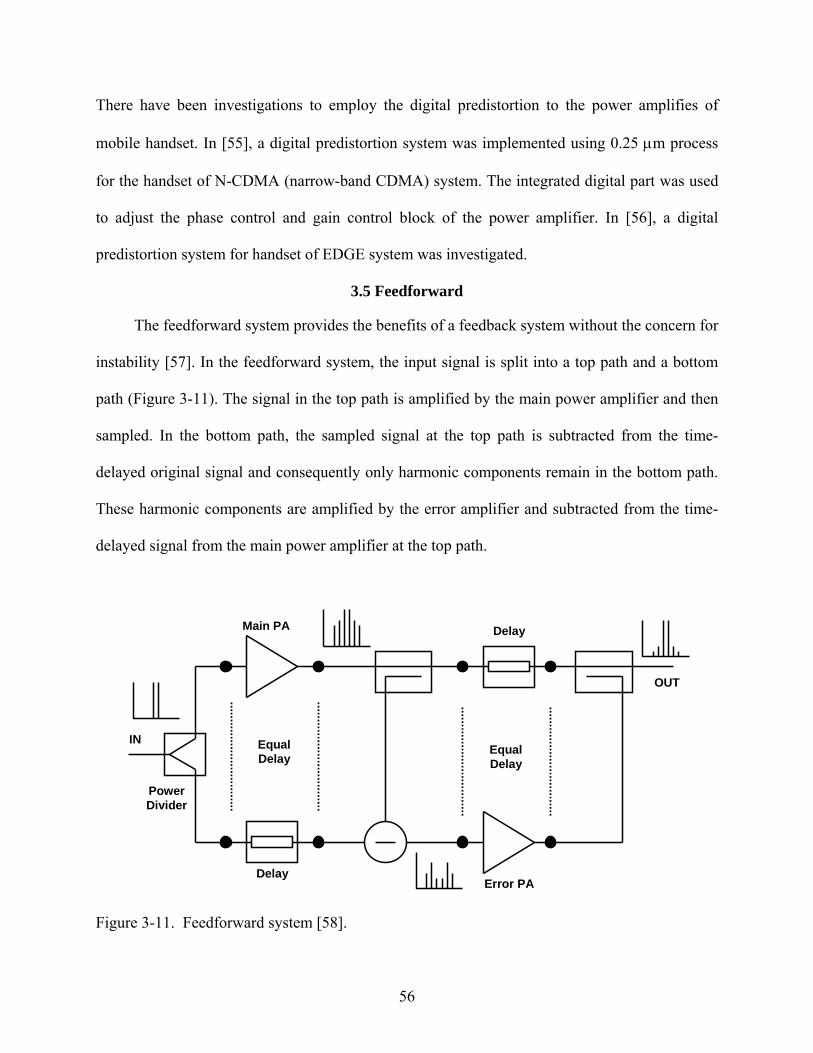
There have been investigations to employ the digital predistortion to the power amplifies of
mobile handset. In [55], a digital predistortion system was implemented using 0.25 µm process
for the handset of N-CDMA (narrow-band CDMA) system. The integrated digital part was used
to adjust the phase control and gain control block of the power amplifier. In [56], a digital
predistortion system for handset of EDGE system was investigated.
3.5 Feedforward
The feedforward system provides the benefits of a feedback system without the concern for
instability [57]. In the feedforward system, the input signal is split into a top path and a bottom
path (Figure 3-11). The signal in the top path is amplified by the main power amplifier and then
sampled. In the bottom path, the sampled signal at the top path is subtracted from the time-
delayed original signal and consequently only harmonic components remain in the bottom path.
These harmonic components are amplified by the error amplifier and subtracted from the time-
delayed signal from the main power amplifier at the top path.
PowerDivider
Delay
DelayMain PA
Error PA
IN
OUT
EqualDelay
EqualDelay
Figure 3-11. Feedforward system [58].
56

The feedforward technique offers superior linearity performance compared to other
linearization techniques. In addition to it, the feedforward system allows the linear operation of
an RF power amplifier over a wide range of bandwidth. The feedforward system also has some
disadvantages. In general, the efficiency of the feedforward amplifier is less than 10 % and so
this system is not applied in applications requiring high efficiency. The feedforward system also
requires several sub-circuit blocks such as power divider, power combiner, and time delay lines,
which are made of the transmission line. Although it is uneasy to employ the feedforward
technique to the power amplifier of the mobile handset, a simulation result of a CMOS power
amplifier with integrated feedforward system was presented in [59].
57

CHAPTER 4 PREDISTORTER USING DIODE-CONNECTED MOSFET
4.1 Background
In this chapter, a novel predistorter linearizer is introduced. In [60], the Schottky diode was
used as the nonlinearity generation circuit for a RF predistorter and that improved the linearity
performance of a power amplifier for the wide band input signal. However, the predistorter in
those papers was demonstrated using compound semiconductor processes and it was not
incorporated with the power amplifier. In this chapter, a kind of the predistorter is proposed for
the linearization of the power amplifier using FET and it has the same configuration as one
developed in [60]. However, in the proposed predistorter, a diode-connected MOSFET is used as
a nonlinearity generation circuit instead of the Schottky diode in [60]. In chapter 7, the
characteristics of the predistorter using the diode-connected MOSFET are compared with the
predistorter using the Schottky diode. The proposed predistorter is compatible with both the
CMOS process and MESFET process. The AM-AM and AM-PM distortion characteristics of the
proposed predistorter are tailored separately for the AM-AM and AM-PM distortion
characteristics of the power amplifier respectively and it is incorporated with the CMOS power
amplifier.
4.2 Basic Configuration of the Predistorter
Figure 4-1 shows the schematic diagram of the proposed predistorter using the diode-
connected MOSFET. C1 and C2 are dc blocking capacitors and RP is used to set the dc voltage at
node P of the diode-connected MOSFET. The RP needs to be as large as several hundreds ohm in
order to prevent the signal loss through the RP. The diode-connected MOSFET of Figure 4-1 is
in the saturation region and it can be represented by a parallel equivalent resistor RV and a
parallel equivalent capacitor CV.
58

OUTIN
C1
VD
C2
≡ RV || CV
RPNode P
OUTIN
C1
VD
C2
≡ RV || CV
RPNode P
Figure 4-1. Basic configuration of predistorter.
4.3 Voltage and Current Swing through FET and Equivalent Elements
Figure 4-2 shows the dynamic impedance line of the predistorter at node P looking into the
drain. The simulation frequency is 2.4 GHz and the width of MOSFET is 40 µm.
0.2 0.4 0.6 0.8 1 1.2-2
0
2
4
6
8
10
12
Cur
rent
thro
ugh
MO
SFET
(mA)
Voltage at Node P (V)
DC voltage at Node Pat Input Power = 5 (dBm)
DC voltage at Node Pat Input Power = -10 (dBm)
At Input Power = 5 (dBm)At Input Power = -10 (dBm)
Figure 4-2. Dynamic impedance line of predistorter.
59

0 0.2 0.4 0.6 0.8
0
0.5
1
1.5
0 0.2 0.4 0.6 0.8-10
-5
0
5
10
0 0.2 0.4 0.6 0.8-10
-5
0
5
10
Voltage
Current
At Input Power = 5 (dBm)At Input Power = -10 (dBm)
Cur
rent
thro
ugh
FET
(mA)
Volta
ge a
t Nod
e P
(V)
Time (ns) Figure 4-3. Voltage and current waveforms of predistorter.
Pav s (-10.000 to 5.000)
Sp
Input Power= 5 dBm
Input Power Range : -10 dBm to 5 dBm
Input Power= -10 dBm
Figure 4-4. Impedance of predistorter on Smith chart.
60

Figure 4-3 shows the time-domain waveforms of the voltage and current swings of the
diode-connected MOSFET. As the input power increases and the ac voltage swing at node P
goes over the threshold voltage of the MOSFET, the voltage swing is limited and the equivalent
resistance RV of the diode-connected MOSFET starts to increases substantially. As the secondary
effect of the nonlinear voltage swing, the dc voltage at node P decreases with the increasing
input power. It is because the voltage swing in the negative cycle increases faster than the
voltage swing in the positive cycle as the input power increases. The impedance variation of the
predistorter is shown on the Smith Chart in Figure 4-4. As the input power increases from -10
dBm, the equivalent resistance RP increases but the equivalent capacitor CV remains relatively
constant. Figure 4-5 shows the equivalent RV and CV of the diode-connected MOSFET. As the
width of the diode-connected MOSFET increases, the equivalent resistance RV decreases while
the equivalent capacitance CV increases.
-10 -5 0 50
20
40
60
80
100
-10 -5 0 50
0.05
0.1
0.15
0.2
Input Power (dBm)
Rv
(Ω)
Cv
(pF)
Rv (W = 30 µm)Rv (W = 40 µm)Rv (W = 50 µm)
Cv (W = 30 µm)Cv (W = 40 µm)Cv (W = 50 µm)
Figure 4-5. Equivalent RV and CV of predistorter.
61

4.4 Large Signal S21 of the Predistorter
The forward transmission scattering parameter (S21) of a two port network can be
expressed by equation 4.1
THO
O
EV
ZZS
,1
2
2
121 2 ⋅⋅= (4.1)
Here, ZO1 and ZO2 are the termination impedances at the input and the output of the
predistorter respectively and E1,TH and V2 are the equivalent voltage at port 1 and port 2
respectively. For the configuration of Figure 4-1, the S21 of the predistorter can be obtained
using the equivalent parameter RV and CV of the diode-connected MOSFET.
21
21
21
2
1
2
1
2
2
121
111112
111112
1111
1111
2
OPVV
O
OO
OPVVO
O
O
OPVV
O
OPVV
O
O
ZRRCj
ZZZ
ZRRCjZ
ZZ
ZRRCj
Z
ZRRCj
ZZ
S
++++⋅
⋅=
+⎟⎟⎠
⎞⎜⎜⎝
⎛+++⋅
⋅⋅=
++++
+++⋅⋅=
ω
ω
ω
ω
(4.2)
The gain and phase of the S21 of the predistorter are expressed by equations 4.3 and 4.4
respectively when both the input and the output of the predistorter are terminated by 50 Ω.
( )2221
11251
1502)50(
VPV
CRR
S
ω+⎟⎟⎠
⎞⎜⎜⎝
⎛++
⋅=Ω (4.3)
⎟⎟⎟⎟⎟
⎠
⎞
⎜⎜⎜⎜⎜
⎝
⎛
⎟⎟⎠
⎞⎜⎜⎝
⎛++
−=Ω∠ −
PV
V
RR
CS
11251
tan)50( 121
ω (4.4)
62

Equation 4.2 shows that as the RV increases, the gain of the predistorter increases.
Meanwhile, equation 4.3 shows that as the RV increases, the negative phase distortion of the
predistorter increases. Equation 4.3 shows that as the CV increases, the phase of the predistorter
increases negatively. Equation 4.3 also indicates that as the input power increases, the phase of
the predistorter increases negatively. Figure 4-6 shows the gain and phase variation of the
predistorter for three different sizes of MOSFETs.
-10 -5 0 5-4
-3
-2
-1
0
-10 -5 0 5-4
-3
-2
-1
0
-10 -5 0 5-4
-3
-2
-1
0
-10 -5 0 5-4
-3
-2
-1
0
Input Power (dBm)
Gai
n (d
B)
Phas
e (d
egre
e)
Gain (W = 30 µm)Gain (W = 40 µm)Gain (W = 50 µm)
Phase (W = 30 µm)Phase (W = 40 µm)Phase (W = 50 µm)
Figure 4-6. Gain and phase of the predistorter.
The increase in CV causes the negative AM-PM distortion of the predistorter to increase
with the increasing input power.
4.5 Phase Characteristic of the Predistorter
Figure 4-7 shows a predistorter with an additional capacitor CP to control the phase
characteristic of the predistorter. As the value of the parallel capacitor increases, the phase
distortion of the predistorter increases negatively as shown in Equation 4.3.
63

OUTIN C1
VDD
C2
RPNode P
Cp
Figure 4-7. Predistorter with an additional parallel capacitor.
Figure 4-8 shows the negative AM-PM distortion of the predistorter for four different
values of parallel capacitor CP.
-10 -5 0 5-12
-10
-8
-6
-4
-2
0
Input Power (dBm)
Phas
e (d
egre
e)
Cp = 0 pF
Cp = 0.2 pF
Cp = 0.4 pF
Cp = 0.6 pF
Figure 4-8. Phase variation of predistorter for four different values of CP.
64

4.6 CMOS Power Amplifier with the Predistorter
Figure 4-9 shows the schematic diagram of the power amplifier with the integrated
predistorter. A predistorter using a diode-connected MOSFET was customized to compensate the
negative AM-AM distortion and the positive AM-PM distortion of the power amplifier. The
widths of the MOSFETs for the power amplifier and the predistorter are 400 µm and 45 µm
respectively. RP, which is used to bias the diode connected MOSFET is 315 Ω. CM is used to
both match the input of the power amplifier and adjust the phase characteristic of the predistorter.
LM is the impedance-matching element. C1 and C2 are the blocking capacitors. The supply
voltages are 1.8 V for both the power amplifier and the predistorter. The low-pass input
impedance-matching network was used to filter out the high frequency spurious responses from
the predistorter. The decrease in gain of the CMOS power amplifier was compensated by the
increase in gain of the predistorter and the increase in phase of the power amplifier is
compensated by the decrease in phase of the predistorter (Figure 4-10).
VDD
VB
C1
VA
C2LM
CM
RP
VDD
VB
C1
VA
C2LM
CM
RP
Figure 4-9. CMOS power amplifier with predistorter.
65

-5 0 5 10 15-1
-0.5
0
0.5
-5 0 5 10 15-1
0
1
2
3
-5 0 5 10 15-1
0
1
2
3
Output Power (dBm)
Rel
ativ
e G
ain
(dB
)
Rel
ativ
e Ph
ase
(deg
ree)Without Linearizer
Witih LineaizerGain
Phase
Figure 4-10. Relative gain and phase of the power amplifier.
-5 0 5 10
-80
-70
-60
-50
-40
-30
-20
Output Power (dBm)
IMD
3 (d
Bc)
Without LinearizerWitih Lineaizer
Figure 4-11. IMD3 characteristic of the power amplifier.
66

When the predistorter is not biased, the small signal gain of the CMOS power amplifier is
14.6 dB. When the predistorter is biased, the small signal gain is 11.3 dB and thus the signal loss
due to the predistorter is 3.3 dB. Because the characteristic of the predistorter was optimized
during the simulation, the loss of the predistorter is pretty small compared to the other
implementation of RF predistorters. With the integrated predistorter, the IMD3 of the CMOS
power amplifier is improved by 27.7 dB at the output power of 0 dBm and by 38 dB at the output
power of 6 dBm (Figure 4-11).
4.7 Experimental Results
The 2.4 GHz CMOS power amplifier designed and analyzed in the previous sections was
fabricated using a 1P6M mixed-mode UMC process (Figure 4-13). The size of the fabricated
chip is 1.73 mm by 1.0 mm. The output power of the power amplifier was decided considering
the metal migration issue. The on-chip measurement was conducted for the characterization of
the power amplifier. The small signal S-parameters of the power amplifier were measured with a
network analyzer.
Figure 4-12. Power amplifier with predistorter.
67

2 2.2 2.4 2.6 2.8-30
-20
-10
0
10
20
Frequency (GHz)
Mag
nitu
de (d
B)
S21S11S22
Figure 4-13. Measured scattering parameters.
-10 -5 0 50
5
10
15
20
-10 -5 0 5 0
5
10
15
20
25
Input Power (dBm)
Out
put P
ower
(dB
m),
Gai
n (d
B)
Power PAE
(%)
PAE
Gain
Figure 4-14. Measured output power, gain, and PAE.
68

When the predistorter is not biased the gain of the power amplifier is 10.9 dB and the input
and output scattering parameters are -16.8 dB and -13.5 dB respectively at the operation
frequency of 2.4 GHz (Figure 4-13). When the predistorter is biased with 0.6 V and 1.8 V, the
gain is dropped by 0.8 dB and 3.1 dB respectively.
The power and efficiency characteristics of the power amplifier were characterized with a
one tone input signal. Figure 4-14 shows the output power, PAE, and the gain of the power
amplifier when the predistorter is not biased. The output P1dB of the power amplifier is 14.0
dBm and the PAE at the output P1dB is 16.3 %. The linearity characteristic of the power
amplifier was measured with a two tone input signal. The block diagram of the on-chip
measurement setup with a two tone signal and the arrangement of the measurement equipments
in the laboratory are shown in Figure 4-15 and Figure 4-16 respectively. The gate and drain bias
voltages for the power amplifier, and the control voltage for the predistorter were applied
through the dc probes.
PA
Probe Station
CalibrationReference
Planes
SignalGenerator
SpectrumAnalyzer
PowerSupply
Vg VdVc
SignalGenerator
PowerCombiner
Figure 4-15. Two tone measurement setup.
69

For the two tone input signal, the resistive power combiner was used because it provides
the constant termination condition over a broad frequency band.
Figure 4-16. Arrangement of measurement equipments.
Figure 4-17 and Figure 4-18 shows the simulated IMD3 and measured IMD3 of the power
amplifier respectively when the diode-connected MOSFET of the predistorter is biased at 0 V,
0.6 V, 0.7 V, and 0.8 V respectively. The measured IMD3s of Figure 4-17 are pretty similar to
the simulated IMD3s of Figure 4-18. When the bias voltage for the predistorter is low, the gain
drop of the power amplifier was slightly over-compensated by the gain expansion of the
predistorter and the gain of the power amplifier with the predistorter showed the slight gain
expansion. When the predistorter is biased at 0.6 volt, the IMD3 of the power amplifier was
improved by 11.7 dB at the output power of the 1.2 dBm.
70

-10 -5 0 5 10-70
-60
-50
-40
-30
-20
Output Power (dBm)
IMD
3 (d
Bc)
VD = 0 V VD = 0.6 V VD = 0.7 VVD = 0.8 V
Figure 4-17. Measured IMD3 characteristic with low bias voltage for the predistorter.
-10 -5 0 5 10-70
-60
-50
-40
-30
-20
Output Power (dBm)
IMD
3 (d
Bc)
VD = 0 V VD = 0.6 V VD = 0.7 VVD = 0.8 V
Figure 4-18. Simulated IMD3 characteristic with low bias voltage for the predistorter.
71

-10 -5 0 5 10-80
-70
-60
-50
-40
-30
-20
Output Power (dBm)
IMD
3 (d
Bc)
VD = 0 V VD = 1.0 V VD = 1.4 VVD = 1.8 V
Figure 4-19. Measured IMD3 characteristic of the high bias voltage for the predistorter.
-10 -5 0 5 10-80
-70
-60
-50
-40
-30
-20
Output Power (dBm)
IMD
3 (d
Bc)
VD = 0 V VD = 1.0 V VD = 1.4 VVD = 1.8 V
Figure 4-20. Simulated IMD3 characteristic of the high bias voltage for the predistorter.
72

When the predistorter is biased at 0.7 volt, the IMD3 of the power amplifier was improved
by 12.6 dB at the output power of the 3 dBm. Figure 4-19 and Figure 4-20 shows the simulated
IMD3 and measured IMD3 of the power amplifier respectively when the diode-connected
MOSFET of the predistorter is biased at 0 V, 1.0 V, 1.4 V, and 1.8 V. Figure 4-19 and Figure 4-
20 illustrate that when the bias voltage of the diode-connected MOSFET of the predistorter goes
high, the measured IMD3s does not follow the simulated IMD3. In the simulation, when the
predistorter is biased by 1.1 V, the gain of the power amplifier with the predistorter showed the
highest gain expansion and when the predistorter is biased by 1.8 V, the gain drop of the power
amplifier is optimally compensated by the slight gain expansion of the predistorter. However, in
the measurement, when the predistorter is biased by 1.8 V, the gain of the power amplifier with
the predistorter still showed the increasing gain with the increasing input power.
When the bias voltage for the predistorter is low, the diode-connected FET of the
predistorter is turned-on only for the small part of the signal swing and the harmonic balance
simulation of the ADS successfully estimates the large signal behavior of the diode-connected
MOSFET. As the bias voltage of the diode-connected MOSFET goes high, the diode-connected
MOSFET is turned-on for the most part of the signal swing and a large amount of the square law
non-linearity is involved with the operation of the diode-connected MOSFET. As a result of it,
the harmonic balance simulation fails to estimate the large signal behavior of the heavily turned-
on diode-connected MOSFET. It also needs to be mentioned that the maximum order of the
frequency component was set to 9 during the harmonic balance simulation and the higher order
components than 9th order were not included.
73

CHAPTER 5 LINEARIZATION OF CASCODE CMOS POWER AMPLIFIER
5.1 Background
For the modern modulation scheme, as well as the AM-AM distortion and the AM-PM
distortion degrade substantially the linearity performance of a power amplifier. The cascode
configuration is frequently used for the radio frequency power amplifier because the cascode
configuration provides high isolation from the input to the output. Thanks to the high isolation
between the input and the output, the stability of the power amplifier improves. With regard to
the large signal operation of MESFET, it was investigated that the common gate FET in the
cascode configuration has the decreasing phase characteristic with the increasing input power
[53]. In other words, the common gate FET has the negative AM-PM distortion characteristic
contrary to the positive AM-PM distortion characteristic of the common source FET.
Gain(PD)
Gain(PA)
Pin Pin
Cascode
Predistorter(PD)
IN OUT
Phase(PD)
PinPin
Phase(PD)
PA
Figure 5-1. Gain and phase characteristics of cascode power amplifier with predistorter.
74

Because of the effect of the common gate stage on the phase distortion, the overall phase
distortion of the cascode power amplifier could show the decreasing phase characteristics with
the increasing input power. Therefore, when a predistorter is used for a power amplifier which
has the negative AM-PM characteristic, the predistorter should have the positive AM-PM
characteristic (Figure 5-1). In this chapter, the diode-connected predistorter is used to linearize
the cascode CMOS power amplifier.
5.2 Control of Phase Characteristic of the Predistorter
Figure 4-6 of the previous chapter shows that the increase in CV causes the phase of the
predistorter to decrease with the increasing input power (negative AM-PM characteristic).
OUTIN
C1
VDD
C2
≡ RV || CGS
RP
LP
Figure 5-2. Predistorter having positive AM-PM characteristic.
By adding an appropriate value of a parallel capacitor at node P of the predistorter, the
negative AM-PM characteristic of the predistorter can be adjusted. On the other hand, by
inserting a parallel inductor at node P of the predistorter, a positive AM-PM characteristic can be
obtained. Figure 5-2 shows a predistorter which includes an inductor component in parallel with
the diode connected MOSFET in order to obtain the positive AM-PM characteristic. C1 and C2
75

are blocking capacitors and these are short circuits at the operation frequency. The phase formula
of the predistorter of Figure 5-1 is shown below.
⎟⎟⎟⎟
⎠
⎞
⎜⎜⎜⎜
⎝
⎛
++
−−=∠ −
PV
PV
RR
LC
S11
251
1
tan 121
ωω
(5.1)
The gain and phase variation of the predistorter of Figure 5-1 are shown in Figure 5-3 for
three different values of parallel inductors. As the value of LP decreases and the 1/(ωLP) becomes
less than ωCV, the phase distortion becomes positive.
-15 -10 -5 0-5
-4.5
-4
-3.5
-3
-2.5
-15 -10 -5 0 -10
-5
0
5
10
15
20
-15 -10 -5 0 -10
-5
0
5
10
15
20
-15 -10 -5 0 -10
-5
0
5
10
15
20
Input Power (dBm)
Gai
n (d
B)
Phas
e (d
egre
e)
Gain (without Lp)Gain (Lp = 3 nH)Gain (Lp = 1 nH)
Phase (without Lp)Phase (Lp = 3 nH)Phase (Lp = 1 nH)
Figure 5-3. Gain and phase of the predistorter with parallel inductor.
Figure 5-4 shows the variation of the forward transmission coefficient (S21) of the
predistorter (Figure 5-2) in polar coordinate as the input power increases. When the parallel
76

inductor LP becomes less than 3 nH, the phase characteristic of the predistorter reverses from the
negative AM-PM distortion to the positive AM-PM distortion.
1 nH
Input Power Range : -15 (dBm) to 4 dBm
3 nH
Without Lp
0º180º
90º
0.51
Figure 5-4. S21 of the predistorter.
5.3 Cascode CMOS Power Amplifier with the Predistorter
A 5.8 GHz cascode power amplifier was designed using a 400-µm FET. Similar to the
cascode power amplifier using MESFET, the designed CMOS cascode power amplifier had the
negative AM-PM characteristic. When a power amplifier has the negative AM-PM characteristic,
the predistorter should have the positive AM-PM characteristic. A predistorter is tailored to the
cascode CMOS power amplifier and integrated with the power amplifier (Figure 5-5). Between
the predistorter and the power amplifier, a low-pass input matching network was used to filter
out the high frequency spurious components from the predistorter. The supply voltage is 1.8 volt
77

for both the power amplifier and the predistorter. The gate bias voltage is 1 V and the resistance
for the gate bias is 1 kΩ.
VDD
VGATEVDD
C1 C2
Figure 5-5. Schematic diagram of the power amplifier.
C1 and C2 in Figure 5-5 are blocking capacitors. An inductor in front of the diode
connected MOSFET controls the positive AM-PM characteristic of the predistorter. Although
not implemented here, a buffer stage can be inserted at the output of the predistorter to suppress
harmonics generated from the predistorter.
5.4 Linearization Performance
Figure 5-6 shows the simulated gain and phase characteristic of the 5.8 GHz cascode
CMOS power amplifier with the predistorter. Similarly to the cascode configuration using
MESFET described in [53], the cascode power amplifier using MOSFET had negative AM-PM
characteristics. The decreasing phase of the cascode power amplifier is compensated with the
increasing phase of the predistorter realized with the additional inductor for the positive phase
control.
78

-10 -5 0 5 10-1
-0.5
0
0.5
1
-10 -5 0 5 10 -4
-3
-2
-1
0
1
-10 -5 0 5 10 -4
-3
-2
-1
0
1
Output Power (dBm)
Rel
ativ
e G
ain
(dB
)
Rel
ativ
e Ph
ase
(deg
ree)
Without LinearizerWitih Lineaizer
Gain
Phase
Figure 5-6. Relative gain and phase of the power amplifier.
-10 -5 0 5 10-80
-70
-60
-50
-40
-30
-20
-10
Output Power (dBm)
IMD
3 (d
Bc)
Without LinearizerWitih Lineaizer
Figure 5-7. IMD3 characteristic of the power amplifier.
79

The gain of the cascode CMOS power amplifier is 11.9 dB when the predistorter is not
biased while the gain of the predistorter is decreased to 8.9 dB when the predistorter is biased by
1.8 V. Figure 5-7 shows the simulated IMD3 of the cascode CMOS power amplifier when the
predistorter is not biased and biased by 1.8 V.
When the linearizer is biased with the 1.8 V, the IMD3 is improved by 25.1 dB at the
output power of -2 dBm and by 29.3 dB at the output power of 2 dBm.
5.5 Experimental Results
The size of the fabricated 5.8 GHz cascode CMOS power amplifier is 1.51 mm by 0.84
mm (Figure 5-8).
Figure 5-8. Power amplifier with predistorter.
When the predistorter is not biased, the gain of the power amplifier is 11.6 dB and the
input and output scattering parameters are -17.0 dB and -3.2 dB respectively at the operation
frequency of 5.8 GHz (Figure 5-9). When the predistorter is biased with 0.6 V and 1.8 V, the
gain is dropped by 1.1 dB and 4.0 dB respectively.
80
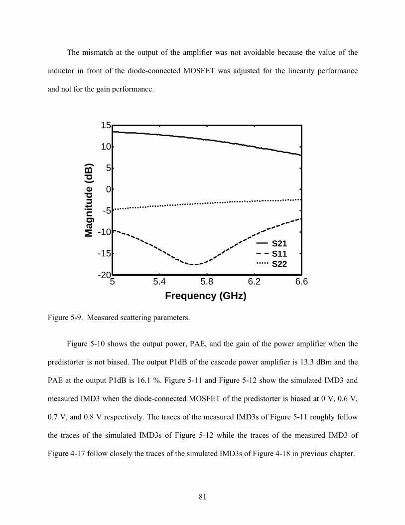
The mismatch at the output of the amplifier was not avoidable because the value of the
inductor in front of the diode-connected MOSFET was adjusted for the linearity performance
and not for the gain performance.
5 5.4 5.8 6.2 6.6-20
-15
-10
-5
0
5
10
15
Frequency (GHz)
Mag
nitu
de (d
B)
S21S11S22
Figure 5-9. Measured scattering parameters.
Figure 5-10 shows the output power, PAE, and the gain of the power amplifier when the
predistorter is not biased. The output P1dB of the cascode power amplifier is 13.3 dBm and the
PAE at the output P1dB is 16.1 %. Figure 5-11 and Figure 5-12 show the simulated IMD3 and
measured IMD3 when the diode-connected MOSFET of the predistorter is biased at 0 V, 0.6 V,
0.7 V, and 0.8 V respectively. The traces of the measured IMD3s of Figure 5-11 roughly follow
the traces of the simulated IMD3s of Figure 5-12 while the traces of the measured IMD3 of
Figure 4-17 follow closely the traces of the simulated IMD3s of Figure 4-18 in previous chapter.
81

-10 -5 0 50
5
10
15
20
-10 -5 0 5 0
5
10
15
20
25
30
Input Power (dBm)
Out
put P
ower
(dB
m),
Gai
n (d
B)
Power PAE
(%)
PAE
Gain
Figure 5-10. Measured output power, gain, and PAE.
-10 -5 0 5 10-65
-60
-55
-50
-45
-40
-35
-30
-25
Output Power (dBm)
IMD
3 (d
Bc)
VD = 0 V VD = 0.6 V VD = 0.7 VVD = 0.8 V
Figure 5-11. Measured IMD3 characteristic with low bias voltage for the predistorter.
82

-10 -5 0 5 10-65
-60
-55
-50
-45
-40
-35
-30
-25
Output Power (dBm)
IMD
3 (d
Bc)
VD = 0 V VD = 0.6 V VD = 0.7 VVD = 0.8 V
Figure 5-12. Simulated IMD3 characteristic with low bias voltage for the predistorter.
-10 -5 0 5 10-80
-70
-60
-50
-40
-30
Output Power (dBm)
IMD
3 (d
Bc)
VD = 0 V VD = 1.0 V VD = 1.4 VVD = 1.8 V
Figure 5-13. Measured IMD3 characteristic with high bias voltage for the predistorter.
83

-10 -5 0 5 10-80
-70
-60
-50
-40
-30
Output Power (dBm)
IMD
3 (d
Bc)
VD = 0 V VD = 0.6 V VD = 0.7 VVD = 0.8 V
Figure 5-14. Simulated IMD3 characteristic with high bias voltage for the predistorter.
The measured S11 of the cascode power was considerably different from the simulated
S11 parameter and it indicates the AM-PM characteristic of the fabricated predistorter for the
cascode power amplifier is deviated from the designed characteristic. Table 5-1 compares the
simulated input and output scattering parameters with the measured input and output scattering
parameters of the power amplifiers of chapter 4 and chapter 5.
Table 5-1. Input and output scattering parameters. 2.4 GHz PA (Chap. 4) 5.8 GHz Cascode PA (Chap. 5)
Simulation Measurement Simulation Measurement
S11 -15.2 dB -16.8 dB -8.5 dB -16.8 dB
S22 -7.5 dB -13.5 dB -5.0 dB -3.2 dB
84

When the predistorter was biased at 0.6 volt, the IMD3 of the power amplifier was
improved by 10.2 dB at the output power of the 2 dBm. When the predistorter was biased at 0.7
volt, the IMD3 of the power amplifier was improved by 12.4 dB at the output power of the 4.6
dBm. Figure 4-19 and Figure 4-20 show the simulated IMD3 and measured IMD3 of the power
amplifier respectively when the diode-connected MOSFET of the predistorter is biased at 0 V,
1.0 V, 1.4 V, and 1.8 V. Similar to the power amplifier in chapter 4, when the bias voltage of the
diode-connected MOSFET is high, the simulation fails to estimate the large signal behavior of
the diode-connected MOSFET. It can be concluded from the measurement results of chapter 4
and chapter 5 that until the accurate model of the diode-connected MOSFET is developed, the
lightly turned-on diode-connected MOSFET could be more appropriate than the heavily turned-
on diode-connected MOSFET for the practical design even though the lightly turned-on diode-
connected MOSFET does not provide the best design result.
85

CHAPTER 6 PREDISTORTER USING MOSFET IN NEAR-COLD FET CONDITION
6.1 Background
Power amplifiers are required to have low distortion and the use of linearization techniques
improves the linearity performance of the power amplifier. Among several linearization
techniques, the predistortion is a simple and stable linearization technique and thus is most
suitable for monolithic integration with power amplifiers.
For a hetero-junction bipolar transistor (HBT) process, the use of active bias circuits
increased the linearity of MMIC power amplifiers [60]-[61]. The purpose of those active bias
circuits is to keep the base voltage at the constant level with the input power and thus prevent the
AM-AM distortion due to the bias voltage drop at the base of a HBT. However, the active bias
circuit is not effective for the FET-based amplifier because the FET does not experience a bias
voltage drop at the gate with the increasing input power. However, this linearization approach is
different from a predistorter linearization in that a predistorter compensates the decreasing gain
of the power amplifier with the increasing gain of the predistorter as the input power increase.
Recently, there have been publications on the implementation of predistorters using a
compound semiconductor process [60]-[61]. However, predistorters in [60]-[61] were fabricated
as discrete MMIC and were not integrated with a power amplifier. In this chapter, we introduce
an integrated predistorter using a MOSFET in near-cold FET condition. The characteristics of
the developed predistorter can be customized for the specific power amplifier being integrated
with. The proposed predistorter is very simple and incorporated with the gate bias circuit of a
power amplifier. Thus the predistorter does not occupy a chip area and is suitable for any
integrated power amplifier using MOSFET or MESFET process.
86

6.2 Basic Configuration of the Predistorter
The schematic diagram of the predistorter using a MOSFET as a nonlinearity generation
circuit is shown in Figure 6-1.
OUTIN
C1 C2
≡ RV ||CV
Node P
VA
OUTIN
C1 C2
≡ RV ||CV
Node P
VA
Figure 6-1. Basic configuration of predistorter.
In Figure 6-1, the MOSFET is in near-cold FET condition and both C1 and C2 are dc
blocking capacitors. Because of the blocking capacitors, the dc current through the predistorter is
zero and thus the power consumption of the predistorter is zero and the drain to source voltage of
the MOSFET is zero. The equivalent circuit of the FET in Figure 3-1 can be represented by the
parallel circuit of an equivalent resistor (RV) and an equivalent capacitor (CV). When the drain to
source bias of a FET is zero and the gate bias is large enough, the equivalent resistance RV of the
FET is a few ohms and the FET is said to be in the cold FET condition. However, a few ohms of
the equivalent resistance RV is too small to be used as the nonlinearity generation circuit for a
predistorter. Thus the gate bias voltage needs to be controlled. Figure 6-2 shows the variation of
the impedance of the FET, looking into the source, with the increasing gate bias voltage from 0.5
V to 1 V. As the gate bias voltage becomes larger than the threshold voltage, the equivalent
resistance RV begins to decrease and the equivalent capacitance remains small.
87

VGS (0.500 to 1.000)
Sp
VA= 1 Volt
VA Range : 0.5 Volt to 1 Volt
VA= 0.5 Volt
Figure 6-2. Impedance variation of predistorter with 0 V drain to source voltage.
For the simulation of the predistorter, 0.9 V is selected for the gate bias for which the
equivalent resistance RV is about 50 Ω. In the meantime, the predistorter using FET in a near-
cold FET condition cannot be implemented using a package type FET device because the
parasitic capacitance from the package is much larger than the equivalent capacitance CV of the
FET in near-cold FET condition. Therefore, the predistorter using the FET in near-cold FET
condition is appropriate for the chip type FET and the FET in MOSFET process.
6.3 Voltage and Current Swing through FET and Equivalent Elements
The predistorter is simulated and fabricated using 0.18 µm 1P6M mixed-mode UMC
CMOS process. The current swing through MOSFET versus voltage swing at node P shows the
gate voltage VA in Figure 6-1 is set to 0.9 V and the width of the FET is 30 µm (Figure 6-3).
88

-0.5 0 0.5 1-6
-4
-2
0
2
4
6
8
DC voltage at Node Pat Input Power = 5 (dBm)
DC voltage at Node Pat Input Power = -10 (dBm)
At Input Power = 5 (dBm)At Input Power = -10 (dBm)
Cur
rent
thro
ugh
FET
(mA
)
Voltage at Node P (V)
Figure 6-3. Dynamic impedance line of predistorter.
0 0.1 0.2 0.3-0.8
-0.4
0
0.4
0.8
0 0.1 0.2 0.3 -12
-8
-4
0
4
0 0.1 0.2 0.3 -12
-8
-4
0
4
Voltage
Current
At Input Power = 5 (dBm)At Input Power = -10 (dBm) C
urre
nt th
roug
h FE
T (m
A)
Volta
ge a
t Nod
e P
(V)
Time (ns) Figure 6-4. Voltage and current waveforms of predistorter.
89

As the input power increases, the current-voltage relation becomes nonlinear and the
fundamental frequency component of the voltage increases faster than the fundamental
frequency component of the current and thus the equivalent resistance RV increases at 5.8 GHz.
Another effect of the nonlinear voltage swing is the dc voltage shift at node P. The time-domain
waveforms of voltage and current swings of the MOSFET are shown in Figure 6-4. As the input
increases, the voltage swing increases higher in the positive cycle than in the negative cycle and
as a result of the nonlinear voltage swing, a positive dc voltage is generated at node P from even
mode harmonics of the voltage swing.
-10 -5 0 5
50
100
150
200
250
300
-10 -5 0 50
0.02
0.04
0.06
0.08
0.1
-10 -5 0 50
0.02
0.04
0.06
0.08
0.1
-10 -5 0 50
0.02
0.04
0.06
0.08
0.1
Input Power (dBm)
Rv
(Ω)
Cv
(pF)
Rv (W = 10 µm)Rv (W = 20 µm)Rv (W = 30 µm)
Cv (W = 10 µm)Cv (W = 20 µm)Cv (W = 30 µm)
Figure 6-5. Equivalent RV and CV of predistorter.
Figure 6-5 shows the equivalent resistance and capacitance of the MOSFET in Figure 6-1
with the increasing input power from -10 dBm to 5 dBm. As the input power increases, the
90
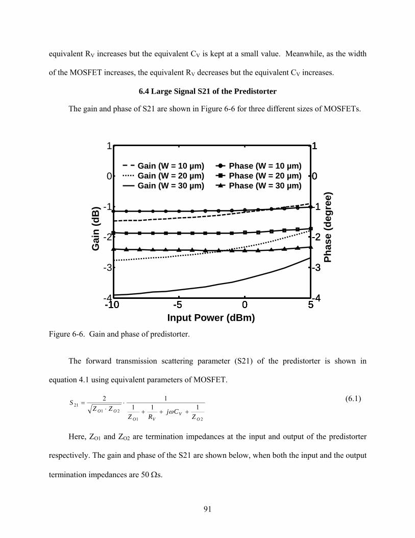
equivalent RV increases but the equivalent CV is kept at a small value. Meanwhile, as the width
of the MOSFET increases, the equivalent RV decreases but the equivalent CV increases.
6.4 Large Signal S21 of the Predistorter
The gain and phase of S21 are shown in Figure 6-6 for three different sizes of MOSFETs.
-10 -5 0 5-4
-3
-2
-1
0
1
-10 -5 0 5-4
-3
-2
-1
0
1
-10 -5 0 5-4
-3
-2
-1
0
1
-10 -5 0 5-4
-3
-2
-1
0
1
Input Power (dBm)
Gai
n (d
B)
Phas
e (d
egre
e)
Gain (W = 10 µm)Gain (W = 20 µm)Gain (W = 30 µm)
Phase (W = 10 µm)Phase (W = 20 µm)Phase (W = 30 µm)
Figure 6-6. Gain and phase of predistorter.
The forward transmission scattering parameter (S21) of the predistorter is shown in
equation 4.1 using equivalent parameters of MOSFET.
21
2121 111
12
OV
VO
OOZ
CjRZ
ZZS
+++⋅
⋅=
ω
(6.1)
Here, ZO1 and ZO2 are termination impedances at the input and output of the predistorter
respectively. The gain and phase of the S21 are shown below, when both the input and the output
termination impedances are 50 Ωs.
91

2221
)(1251
1502
VV
CR
S
ω+⎟⎟⎠
⎞⎜⎜⎝
⎛+
⋅= (6.2)
⎟⎟⎟⎟
⎠
⎞
⎜⎜⎜⎜
⎝
⎛
+−=∠ −
V
V
R
CS 1251tan 1
21ω (6.3)
Equation 6.2 shows that as RV increases the loss due to the predistorter decreases and the
gain increases. Equation 6.2 also shows that as CV increases the signal loss due to the predistorter
increases. Equation 6.3 shows that the phase of the predistorter has the negative AM-PM
distortion and as the CV increases the negative AM-PM distortion increases.
6.5 Phase Characteristic of the Predistorter
In general, the phase of a power amplifier using FET increases as the input power
increases (positive AM-PM distortion) [53] and thus the predistorter should have negative AM-
PM characteristics.
OUTIN
C1 C2
≡ RV ||CV
Node P
VA
Cp
Figure 6-7. Predistorter with an additional parallel capacitor.
Equation 6.2 shows that as the input power increase, the negative AM-PM distortion of the
proposed predistorter increases and thus compensates the positive AM-PM distortion of a power
92

amplifier. When the CV in Figure 6-1 is too small to compensate the positive AM-PM phase
distortion of the power amplifier, the phase characteristic of the predistorter can be adjusted by
adding an additional capacitor to the predistorter. Figure 6-7 shows a predistorter with an
additional parallel capacitor CP at the node P. The phase variations of the predistorter are shown
in Figure 6-8 for four different values of the capacitor CP.
-10 -5 0 5-15
-10
-5
0
Input Power (dBm)
Phas
e (d
egre
e)
Cp = 0 pF
Cp = 0.1 pF
Cp = 0.2 pF
Cp = 0.3 pF
Figure 6-8. Phase variation of predistorter for four different sizes of CP.
6.6 CMOS Power Amplifier with the Predistorter
The designed 5.8 GHz CMOS power amplifier was integrated with the predistorter using
MOSFET in near-cold FET condition (Figure 6-9). The drain bias voltage of the power amplifier
is 1.8 V. The width of the MOSFET for the power amplifier is 400 µm and the width of the
MOSFET of the predistorter is 25 µm. When the VA and VB are not biased and the VC is biased
at 1 V, the power amplifier operates without the linearization. However, when the VA and VB are
93

biased by 2 V and 1 V respectively and the VC is not biased, the power amplifier is linearized by
the predistorter. The values of resistors R1 and R2 are 31 Ω and 1 kΩ respectively and the C1 is
a dc blocking capacitor.
VDDVCVBVA
C1 R1
R2
Node P
Cp
Figure 6-9. CMOS power amplifier with predistorter.
Due to the nonlinear operation of the predistorter, the dc voltage at node P of Figure 6-9
increases slightly with the increasing input power. The dc voltage at node P is 0.94 V at the
output power of -15 dBm and 1 V at the output power of 2 dBm. Figure 6-10 shows the relative
gain and phase of the designed CMOS power amplifier. When the predistorter is biased, the
negative AM-AM distortion of the power amplifier is compensated by the positive AM-AM
distortion of the predistorter. The positive AM-PM characteristic of the predistorter is controlled
by the CP of 0.12 pF of Figure 6-9. When the predistorter is not biased, the simulated small
signal gain of the power amplifier is 11.5 dB and when the predistorter is biased by VA of 2 V
and VB of 1 V, the gain is decreased to 9.5 dB.
94

-5 0 5 10 15-1
-0.5
0
0.5
-5 0 5 10 15-1
0
1
2
3
4
-5 0 5 10 15-1
0
1
2
3
4
Output Power (dBm)
Rel
ativ
e G
ain
(dB
)
Rel
ativ
e Ph
ase
(deg
ree)Without Linearizer
Witih LineaizerGain
Phase
Figure 6-10. Relative gain and phase of the power amplifier.
-5 0 5 10-80
-70
-60
-50
-40
-30
-20
-10
Output Power (dBm)
IMD
3 (d
Bc)
Without LinearizerWitih Lineaizer
Figure 6-11. IMD3 characteristic of the power amplifier.
95
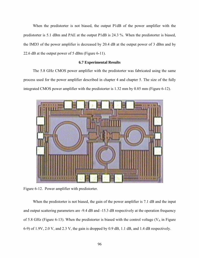
When the predistorter is not biased, the output P1dB of the power amplifier with the
predistorter is 5.1 dBm and PAE at the output P1dB is 24.3 %. When the predistorter is biased,
the IMD3 of the power amplifier is decreased by 20.4 dB at the output power of 3 dBm and by
22.6 dB at the output power of 5 dBm (Figure 6-11).
6.7 Experimental Results
The 5.8 GHz CMOS power amplifier with the predistorter was fabricated using the same
process used for the power amplifier described in chapter 4 and chapter 5. The size of the fully
integrated CMOS power amplifier with the predistorter is 1.32 mm by 0.85 mm (Figure 6-12).
Figure 6-12. Power amplifier with predistorter.
When the predistorter is not biased, the gain of the power amplifier is 7.1 dB and the input
and output scattering parameters are -9.4 dB and -15.3 dB respectively at the operation frequency
of 5.8 GHz (Figure 6-13). When the predistorter is biased with the control voltage (VA in Figure
6-9) of 1.9V, 2.0 V, and 2.3 V, the gain is dropped by 0.9 dB, 1.1 dB, and 1.4 dB respectively.
96
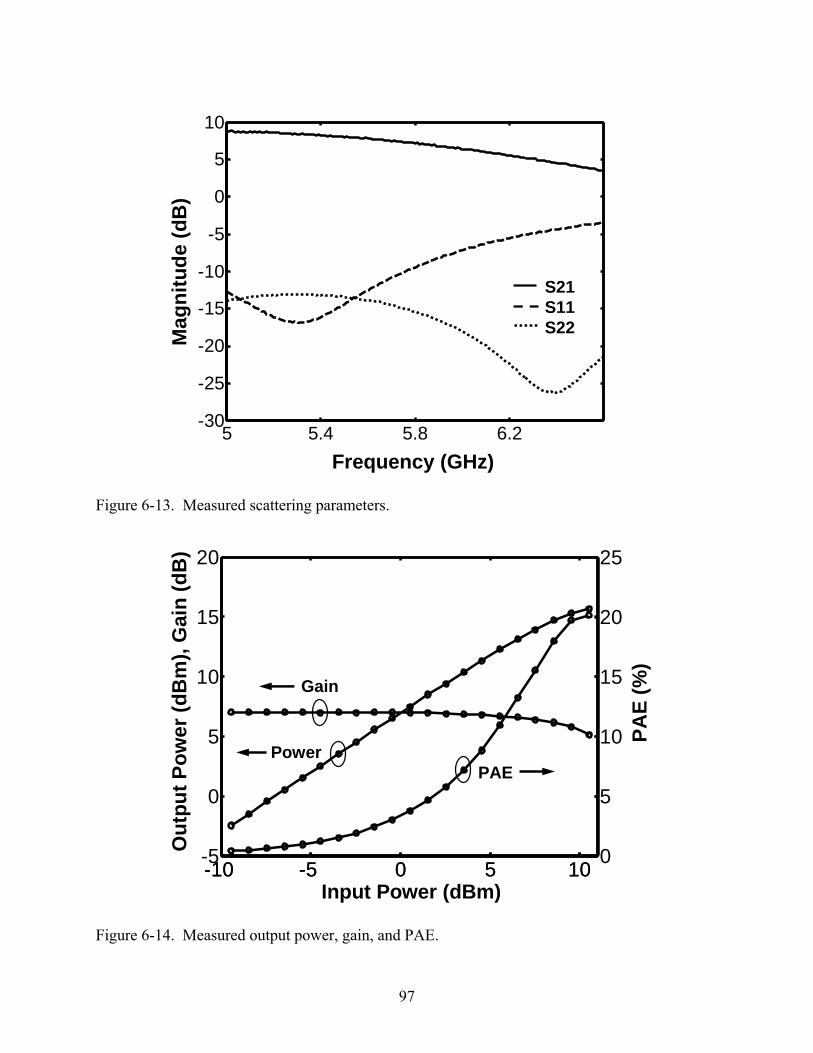
5 5.4 5.8 6.2-30
-25
-20
-15
-10
-5
0
5
10
Frequency (GHz)
Mag
nitu
de (d
B)
S21S11S22
Figure 6-13. Measured scattering parameters.
-10 -5 0 5 10-5
0
5
10
15
20
-10 -5 0 5 10 0
5
10
15
20
25
Input Power (dBm)
Out
put P
ower
(dB
m),
Gai
n (d
B)
Power
PAE
(%)
PAE
Gain
Figure 6-14. Measured output power, gain, and PAE.
97

-10 -5 0 5 10-70
-60
-50
-40
-30
Output Power (dBm)
IMD
3 (d
Bc)
VA= 0 V VA = 1.9 V VA = 2.0 V VA = 2.3 V
Figure 6-15. Measured IMD3 characteristic.
-10 -5 0 5 10-70
-60
-50
-40
-30
Output Power (dBm)
IMD
3 (d
Bc)
VA = 0 V VA = 1.9 V VA = 2.0 VVA = 2.3 V
Figure 6-16. Simulated IMD3 characteristic.
98

The bias voltage VB in Figure 6-9 was set to 1 V. Figure 6-14 shows the measured output
power, PAE, and the gain of the power amplifier when the predistorter is not biased. The output
P1dB of the power amplifier is 14.9 dBm and the PAE at the P1dB is 18.5 %. Figure 6-15 and
Figure 6-16 shows the simulated IMD3 and measured IMD3 of the power amplifier respectively
when the diode-connected MOSFET of the predistorter is biased with the control voltage (VA) of
0 V, 1.9 V, 2.0 V, and 2.3 V respectively. Differently from the power amplifier linearized with
the diode-connected predistorter, the power amplifier linearized with the near-cold FET showed
the IMD3 improvement over the entire output power range. In the design, the predistorter was
optimized with the control voltage of 2.0 V. In the measurement, the maximum IMD3
improvement was obtained with the control voltage of 1.9 V. When the control voltage was set to
1.8 V, the near-cold FET was nearly turned off and the drain current of the power amplifier was
decreased to 27 mA. When the predistorter is biased with the control voltage of 1.9 V, the IMD3
of the power amplifier was improved by 5.6 dB at the output power of the -1 dBm. Although the
power amplifier linearized with the predistorter using the near-cold FET showed the IMD3
improvement over all the output power range, the measurement results are significantly different
from the simulation results.
In the design of the developed predistorter, the equivalent capacitor of the FET was small
and an additional passive capacitor was added to control the phase characteristic of the
predistorter. The equivalent capacitor of the FET is very linear element as it is shown in the
simulation. The added passive capacitor is also very linear element because the metal-insulator-
metal type capacitor is used for the power amplifier design. Therefore, the equivalent resistance
of the MOSFET was the main reason of the discrepancy between the simulation result and the
measurement result. In conclusion, in order to achieve the improved measurement result, the
99

large signal models of the MOSFET in cold-FET condition needs to be improved, because the
predistorter linearization mechanism inevitably involves the highly nonlinear operation of the
MOSFET.
100

CHAPTER 7 COMPARISON AMONG PREDISTORTERS AND STATE OF ART CMOS
PREDISTORTERS
7.1 Comparison between Developed Predistorters
In this section, the predistorter using MOSFET in near-cold FET condition, the predistorter
using a diode-connected MOSFET, and the predistorter using the Schottky are compared.
7.1.1 Comparison between Predistorter using the Diode-Connected MOSFET and Predistorter using the Schottky Diode.
Although a Schottky diode is used in the configuration of Figure 4-1, its low parasitic
capacitance is not an advantage at several giga hertz range because the appropriate value of the
reactance is required in parallel with the Schottky diode to adjust the phase characteristic of the
predistorter. Besides that, the I-V relation of the Schottky diode has the exponential
characteristic and the I-V relation of the diode-connected MOSFET has the square-law
characteristic. On the other hand, the I-V relation of the power amplifier using the BJT or HBT
has the exponential characteristic and the I-V relation of the power amplifier using the MOSFET
has the square-law characteristic. Therefore, the nonlinear characteristic of the diode-connected
MOSFET is similar to the nonlinear characteristic of the CMOS power amplifier and the
nonlinear characteristic of the Schottky diode is similar to the nonlinear characteristic of the BJT
power amplifier. In general, the predistorter using a diode-connected MOSFET is more suitable
than the predistorter using the Schottky diode to compensate the square-law non-linearity of the
CMOS power amplifier.
7.1.2 Comparison between Predistorter using MOSFET in Near-Cold FET Condition and Predistorter using the Diode-Connected MOSFET
The predistorter using the diode-connected MOSFET has better performance for the
linearization than the preditorter using the MOSFET in near-cold FET condition because the
nonlinear characteristic of the diode-connected MOSFET is more similar to the nonlinear
101

characteristic of the CMOS power amplifier. In terms of the power consumption, the power
consumption of the predistorter using the diode-connected MOSFET is 5.9 mW in the design of
chapter 4, while the power consumption of the predistorter using the MOSFET in near-cold FET
condition is zero. However, the power consumption of the CMOS power amplifier itself is 138
mW in the design of chapter 4. Thus the efficiency degradation due to the predistorter using the
diode connected MOSFET is not significant.
7.2 Integrated RF and IF Predistorters
This section describes the linearization performance of the state of art RF and IF
predistorters which is implemented as an integrated circuit.
7.2.1 State of Art IF Predistorter
In [62], an IF predistorter was implemented using a 0.35-µm CMOS process. The
predistorter was an analog type and operated at an IF of 200 MHz with signal bandwidths of
several MHz. The analog predistorter circuit realized a 5th order polynomial function for a
linearization of a power amplifier. The predistorter was located in front of a drive stage and
compensated the distortion of a Mini-Circuit’s MAR-1 class A power amplifier. For the test, the
coefficients of polynomials were set manually through a PC using MATLAB and the Data
Acquisition Toolbox. When the analog predistorter is operated, IMD3 of the power amplifier
was improved by mode than 30 dB and IMD5 was improved by 5 dB.
7.2.2 State of Art RF Predistorter
In [60], a predistorter using the Schottky diode was implemented as an integrated circuit
and it was used to linearize a 18 GHz-band power amplifier. The power amplifier with the
predistorter showed a 20 dB improvement in the IMD3 measurement at the output power of 15
dBm. In [61], a predistorter was implemented using a hetero-junction FET was implemented
with a compound semiconductor process. The FET was placed in series with a signal path and
102

used to linearize a power amplifier using a hetero-junction FET. The power amplifier with the
predistorter showed a 5.7 dBc improvement in ACPR measurement at the output power of 26.2
dBm. However, the power amplifier with the predistorter of [60] showed the improvement of
ACPR only over a certain output power range and not over an entire output power range. In
practice, it is difficult to control both the AM-AM and AM-PM characteristics of the predistorter
using the configuration of [60].
7.2.3 Bias Stabilization using Active Bias Circuit
The purpose of active bias circuits is to keep a bias voltage at a constant level. The base
bias voltage of a bipolar transistor (BJT) decreases with the increasing input power and this
voltage drop at the base of the BJT causes the distortion of the power amplifier. When the active
bias circuit is used to keep the bias voltage at a constant level, the distortion due to the bias
voltage drop can be prevented. For the hetero-junction bipolar transistor (HBT) process, the use
of active bias circuits significantly increased the linearity performance of MMIC power
amplifiers [63]-[64]. In [65], an active bias circuit was used to stabilize the gate bias of a CMOS
power amplifier using 0.25 µm CMOS process. In [65], a diode-connected NMOS transistor was
used to stabilize the gate bias of a 2.4 GHz CMOS power amplifier. With the linearizer, the
power amplifier shows the improvement of ACPR. The maximum improvement of ACPR was
around 5 dBc at the output power of 6 dBm. It needs to be noted that the linearization approach
using the active bias circuit is different from a predistorter linearization in that the predistorter
compensates the decreasing gain of the power amplifier with the increasing gain of the
predistorter as the input power increases. In conclusion, the active bias stabilization is a very
effective method to improve the linearity performance of the power amplifier using the BJT.
However, differently from the BJT, the FET has very high impedance at the gate and the bias
103

voltage drop at the gate with the increasing input power is not noticeable. Thus the active bias
stabilization is not an effective method for the linearization of the power amplifier using FET. In
the simulations conducted using UMC 0.18 µm process and TSMC 0.18 µm process which are
available to us, the power amplifier does not show the gate bias voltage drop with the increasing
input power.
104

CHAPTER 8 HIGH EFFICIENCY POWER AMPLIFIERS
8.1 Background
For mobile systems operating on battery, the efficiency of the power amplifier is one of the
main concerns in the design of the system. The efficiency of the power amplifier is determined
by the input signal, the load impedance, and the conduction angle. When a transistor is
overdriven, the efficiency increases at the expense of the degraded linearity. The class B, class C,
class E, and class F are overdriven power amplifiers. In particular, the class D, class E, and class
F amplifier are called switch mode amplifiers because the transistors of those amplifiers act like
switches. The drain efficiency of the switching mode power amplifier is ideally 100 %. However,
the linearity of the switching mode power amplifier is always poor because the switching activity
of the transistor necessarily involves the harmonic components of the fundamental signal.
The output amplitudes of the class AB, class B, and class C amplifier follow the input
amplitudes, although the output signals of these amplifiers contain some harmonic components.
Contrary to this situation, the output amplitude of the switching mode amplifier has constant
amplitude which is only dependent on supply voltages. Therefore, the switching mode amplifier
can not be used for amplitude modulated signals [66]. In most of the modulation schemes for
mobile communication systems, the amplitude as well as the phase are modulated and thus the
switching mode amplifier cannot be employed for these systems. However, the switching mode
amplifier can be used for a constant envelope signal in which only the phase is modulated.
Besides that, the switching mode amplifier is used for the nonlinear and high efficiency
amplification of the envelope signal in the linear amplification using nonlinear components
(LINC) system proposed by Chireix [67]. The switching mode amplifier was also used for the
amplitude modulation in the envelope elimination and restoration (EER) proposed by Kahn.
105

8.2 Class A and Class B Power Amplifier
A general schematic of a single-ended RF power amplifier with the input and output
matching networks is shown in Figure 8-1.
VDD
MatchingNetwork
MatchingNetwork
Rload
VG
L C
CVout
Vin
R
Zopt
Figure 8-1. A single-ended RF power amplifier.
In the power amplifier of Figure 8-1, C is a blocking capacitor, L is a RF choke inductor, R
is a gate bias resistor, Rload is a load resistance, and Zopt is the optimum impedance seen at the
output of the active device. For a class A amplifier, a transistor is biased at half drain bias current
and the conduction angle is 2π and thus the output waveform perfectly follows the input
waveform. The output power and drain efficiency of the class A amplifier are determined as
equation 8.1
L
DDL
MAXPEAKPEAKClassAout R
VRIIVP 122
122
121 22
, ⋅⎥⎦⎤
⎢⎣⎡⋅=⋅⎥⎦
⎤⎢⎣⎡⋅=⋅⋅=
%5021
2
221
max
max
,
, ==⋅
⋅⋅== IV
IV
PP
DD
DD
ClassAdc
ClassAoutClassAη (8.1)
106

When the knee voltage is taken into account, the output power and drain efficiency are
decreased as
L
KNEEDDPEAKPEAKClassAout R
VVIVP 122
121 2
, ⋅⎥⎦⎤
⎢⎣⎡ −⋅=⋅⋅= (8.2)
%50
2
2)(
21
max
max
,
, <⋅
⋅−⋅==
IV
IVV
PP
DD
KNEEDD
ClassAdc
ClassAoutClassAη (8.3)
In many cases, the efficiency of the power amplifier using a wide bandgap device is
significantly better than the efficiency of the power amplifier using a conventional device. The
main reason of the efficiency increase is the high bias voltage in the power amplifier using a
wide bandgap device. As the drain bias voltage increases, the effect of the knee voltage becomes
small and the efficiency of the power amplifier improves as it can be expected from equation 8.2
and 8.3 [68]. The load lines of the class A, class AB, class B, and class C amplifier are shown in
Figure 8-2.
Imax
VDS
AB
VDDVknee
ABC
Figure 8-2. Road-lines of class A, class B, class AB, and class C amplifier.
107

When the adverse effect of knee voltage (VKNEE) is ignored, the drain efficiency of the
class B amplifier is obtained as
%5.784
221
,
, ==⋅
⋅⋅==
π
π
ηMAX
DD
MAXDD
ClassBdc
ClassBoutClassB IV
IV
PP
(8.4)
In the class B amplifier, the dc current becomes Imax/π and the drain efficiency of the class
B is improved by π/2 factor compared to that of the class A amplifier. However, the gain of the
class B amplifier is less than the gain of the class A amplifier and eventually the improvement in
PAE of the class B amplifier is not as significant as the improvement in drain efficiency. Besides,
the class B amplifiers create large amounts of distortion and thus they are only rarely used for RF
linear amplifiers. The class B amplifier is most commonly used in the "push-pull" configuration
for audio power amplifiers. The push-pull configuration has excellent efficiency, but still suffers
from a distortion called crossover distortion [69].
8.3 Class C Power Amplifier
The class C amplifier conducts less than 180° and has less dc current than the class B
amplifier. Thus, the drain efficiency of the class C power amplifier is better than the class B
power amplifier. The drain efficiency of the class C power amplifier can be obtained using the
following formula [70].
2cos
22sin
sin41
θθθθθη⋅−
−⋅=ClassC (8.5)
where, θ is the conduction angle. From equation 8.5, for the conduction angle of 90°, the
drain efficiency is 94.0 % and for the conduction angle of 45°, the drain efficiency increases to
98.5 %. One drawback of the class C amplifier is that the fundamental current of the class C
108

amplifier is less than that of the class A and class B amplifiers. The less current of the class C
amplifier leads to less output power and less gain. The class C power amplifier is hardly used in
microwave frequency in which the gain has significant importance. Secondly, the class C power
amplifier has high levels of harmonic components at the output. Since the output signal does not
follow the input signal linearly, the class C power amplifier can be used only for frequency
modulated signals such as FM and filtered FSK.
Table 8-1 shows the classification and characteristics of the class A, class AB, class B, and
class C amplifier.
Table 8-1. Classification of amplifiers.
Class Operation
Modes
Conduction
Angle
Maximum
Drain Efficiency Linearity
A 2π (100 %) 50 % Excellent
AB π-2π (50-100 %) 50-78.5 % Good
B π (50 %) 78.5 % Moderate
C
Current
Source
0-π (0-50 %) 100 % Poor
8.4 Class D Power Amplifier
The class D amplifier requires two transistors and both transistors (T1 and T2) are biased
at the class B bias point [71] (Figure 8-3). When transistors are driven differentially and
sufficiently hard, they function as switches and the amplifier works similar to a push-pull class B
amplifier. A filter is required at the output to remove unwanted spectral components generated
from the switch operation of the transistor. The switch operation also requires parasitic drain-
source capacitances at the output of transistors to be charged and discharged without time delay.
In practice, the parasitic drain-source capacitance always leads to power dissipation. When the
109

switch is turned on, the energy charged on the parasitic drain-source capacitance and the energy
dissipation in the switch are represented equation 8.6 and equation 8.7 respectively.
Filter
VDD
Rload
Vout
Vin
- VDD
Figure 8-3. A class D amplifier.
2
21 VCE DSC ⋅⋅= (8.6)
2
21 VCfP DSnDissipatio ⋅⋅⋅= (8.7)
The push-pull operation of the class D amplifier also requires a transformer at the input of
the amplifier and the feasible operation frequency of the class D amplifier is significantly limited
by the transformer [72]. Currently, the use of the class D amplifier is only limited to the audio
amplifiers.
8.5 Class E Power Amplifier
The class E amplifier was published in 1975 by its inventors, Nathan O. Sokal and Alan D.
Sokal. The transistor of the class E power amplifier functions as a switch and the input drive
signal for the class E amplifier may be square wave or sine wave of sufficient amplitude.
110

Differently from the class D amplifier, the class E amplifier only requires one transistor. The
schematic of the amplifier, voltage waveform, and current waveform of the transistor are shown
in Figure 8-4. Like the class D amplifier, the class E amplifier requires a series LC resonator
circuit at the output to remove harmonic components. The current and voltage waveform of the
transistor are shaped by particular passive elements of which equations are derived
mathematically in the time domain by its inventors [73].
VDD
RL
Vout
MatchingNetwork
VG
Vin
Rbias
Lchoke
C
0 π 2π
vS(ωt)
iS(ωt)
vS(ωt)
iC(ωt)iS(ωt)
Figure 8-4. A class E amplifier.
The current through the capacitor C of Figure 8-4 can be written as
)sin()( ϕωω ++= tIIti RDCC (8.8)
and the voltage across the transistor of Figure 8-4 is equal to the voltage across the
capacitor.
111

∫=t
CS tdtiC
tvω
πωω
ωω )(1)( (8.9)
For the dissipation of the transistor to be zero, two conditions of equations 8.10 and 8.11
need to be met.
0|)( 2 == πωω tS tv (8.10)
0|)(
2 == πωωω
tS
tdtvd (8.11)
Equations 8.10 and 8.11 dictate that the voltage across the transistor and the derivative of
the voltage need to be zero when the transistor turns on. Applying these conditions, the values of
parallel capacitance (C), the series inductance (L), and the output power are obtained as [74]
ωωππ LL RRL ⋅≈⋅
−= 1525.1
16)4( 2
(8.12)
LL RRC
ωωππ11836.01
)4(82 ⋅≈⋅+
= (8.13)
L
DD
L
DDOUT R
VR
VP22
2 5768.0)4(
8⋅≅⋅
+=
π (8.14)
and the impedance load required at the output of the transistor can be approximated as
( 1525.11 jRZ LL +⋅= ) . (8.15)
Differently from the class D amplifier, in the class E amplifier, the drain to source
capacitance of the transistor can be taken into account as a design parameter because the drain to
source capacitor can be absorbed into the parallel capacitor C of Figure 8-4. Therefore, the class
E amplifier can operate at higher frequency than the class D amplifier.
112

The major drawback of the class E amplifier is that the peak voltage of the transistor in the
class E amplifier is higher than the drain bias voltage. The peak voltage and peak current of the
transistor are given by
DDDDPEAKS VVv ⋅≈⋅⎥⎦
⎤⎢⎣
⎡⎟⎠⎞
⎜⎝⎛−= 5620.3
2arctan
22,
πππ
(8.16)
DCDCPEAKS IIi ⋅≈⋅⎥⎥⎦
⎤
⎢⎢⎣
⎡+
+= 8621.21
242
,π (8.17)
This peak voltage is larger than the peak voltage of the class A, class B, class D, class F,
and inverse class F amplifier.
8.6 Class F Power Amplifier
The class F amplifier is another switching mode amplifier and has become popular in
recent times. The transistor of the class F amplifier is biased at the class B bias condition and is
driven by a sine or a square wave. The class F amplifier employs the harmonic components at the
output of the transistor in order to shape the voltage and current wave forms. There are two types
of the class F amplifiers. One is a normal type of the class F amplifier and the other is an inverse
class F amplifier. The inverse class F amplifier was investigated mostly for the power amplifier
for low voltage applications [75].
113

VDD
RL
Vout
Lchoke
vS(ωt)
iS(ωt)Vin Resonator
at 3-rdharmonic
Resonatorat 5-th
harmonic
Tank tunedat fundamental
Cblock
Figure 8-5. A class F amplifier.
The class F amplifier implemented using lumped elements is shown in Figure 8-5. The
ideal impedance conditions at the output of the transistor of the normal type of the class F
amplifier are
harmonicsevenallforCircuitShortZ )(0=
harmonicsoddallforCircuitOpenZ )(∞=
When the above conditions are satisfied, the output voltage at the drain of the transistor
becomes a square waveform and the output current at the drain of the transistor becomes a half
sinusoidal waveform (Figure 8-6). Thus, the output voltage only contains odd harmonic
components and the fundamental component and the output current only has even harmonic
components [76].
114

0
vS(ωt) iS(ωt)
0 π 2π π 2π
π⋅IDC
ωt ωt
2⋅VDD
Figure 8-6. Voltage and current waveform at the output of the transistor of the class F amplifier.
Similarly, the ideal impedance conditions at the output of the transistor of the inverse class
F amplifier are
harmonicsevenallforCircuitOpenZ )(∞=
harmonicsoddevenforCircuitOpenZ )(∞=
When the above conditions are satisfied, the output voltage at the drain of the transistor
becomes a half sinusoidal waveform and the output current at the drain of the transistor becomes
a square waveform (Figure 8-7). The one drawback of the inverse class F amplifier is the high
peak voltage of the transistor. The other drawback is that the short circuit termination for all odd
harmonics for the inverse class F amplifier cannot be provided. Contrary to it, short circuit
termination for all even harmonics for the class F amplifier can be realized easily using a
transmission line.
0
vS(ωt) iS(ωt)
0 π 2ππ 2π
π⋅VDC
ωtωt
2⋅IDC
115

Figure 8-7. Voltage and current waveform at the output of the transistor of the inverse class F amplifier.
116
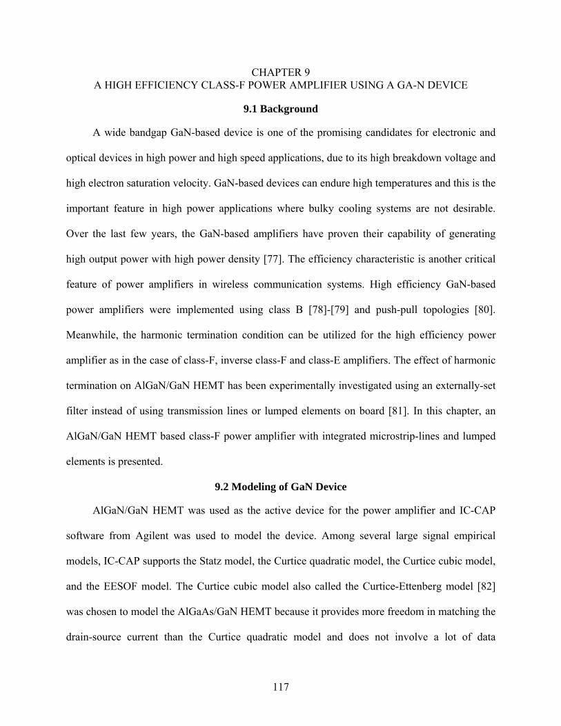
CHAPTER 9 A HIGH EFFICIENCY CLASS-F POWER AMPLIFIER USING A GA-N DEVICE
9.1 Background
A wide bandgap GaN-based device is one of the promising candidates for electronic and
optical devices in high power and high speed applications, due to its high breakdown voltage and
high electron saturation velocity. GaN-based devices can endure high temperatures and this is the
important feature in high power applications where bulky cooling systems are not desirable.
Over the last few years, the GaN-based amplifiers have proven their capability of generating
high output power with high power density [77]. The efficiency characteristic is another critical
feature of power amplifiers in wireless communication systems. High efficiency GaN-based
power amplifiers were implemented using class B [78]-[79] and push-pull topologies [80].
Meanwhile, the harmonic termination condition can be utilized for the high efficiency power
amplifier as in the case of class-F, inverse class-F and class-E amplifiers. The effect of harmonic
termination on AlGaN/GaN HEMT has been experimentally investigated using an externally-set
filter instead of using transmission lines or lumped elements on board [81]. In this chapter, an
AlGaN/GaN HEMT based class-F power amplifier with integrated microstrip-lines and lumped
elements is presented.
9.2 Modeling of GaN Device
AlGaN/GaN HEMT was used as the active device for the power amplifier and IC-CAP
software from Agilent was used to model the device. Among several large signal empirical
models, IC-CAP supports the Statz model, the Curtice quadratic model, the Curtice cubic model,
and the EESOF model. The Curtice cubic model also called the Curtice-Ettenberg model [82]
was chosen to model the AlGaAs/GaN HEMT because it provides more freedom in matching the
drain-source current than the Curtice quadratic model and does not involve a lot of data
117

measurement which is needed for the EESOF model. The drain-source current formula of the
Curtice cubic model is
)(tanh)( 313
212110 dsds VVAVAVAAI ⋅⋅⋅+⋅+⋅+= γ (7.1)
where
([ dsdsgs VVVV −⋅+⋅= 01 1 ) ]β (7.2)
The drain-source current equation of the Curtice cubic model includes polynomial
coefficients A0, A1, A2, and A3 to fit the mathematical drain-source current to the measured one.
V1 of equation 7.2 is used to model the change in pinch-off voltage with drain-source voltage,
Vds0 is the drain-source voltage in saturation at which A0, A1, A2, and A3 are evaluated, and
parameter β is a curve fitting constant. The hyperbolic tangent of the drain-source voltage times
another fitting constant γ controls the slope of drain-source current in the linear region.
The Curtice cubic model also includes the gate-source capacitance, gate-drain capacitance,
drain-source capacitances, and series resistances at the gate, the source, and the drain to
characterize the ac behavior of the active device. These parameters were extracted from the S-
parameter measurement of the device at pinch-off condition, cold-FET condition, and normal
bias conditions. AlGaN/GaN HEMT fabricated at the Air Force laboratory has the 0.75 µm gate
length and 300 µm gate width (Figure 9-1).
S
G
S
S
D
S
Figure 9-1. AlGaN/GaN HEMT from Air Force.
118

freq (50.00MHz to 4.200GHz)
Mea
sure
d.S
(1,1
)M
easu
red.
S(2
,2)
S(2
,2)
S(1
,1)
S22 : MeasuredS22 : Modeled
Frequency Range : 50 MHz to 4.2 GHz
S11 : MeasuredS11 : Modeled
Figure 9-2. S11 and S22.
-3 -2 -1 0 1 2 3-4 4
freq (50.00MHz to 4.200GHz)
Me
asu
red
..S(2
,1)
S(2
,1)
S21 : MeasuredS21 : Modeled
Frequency Range : 50 MHz to 4.2 GHz
Figure 9-3. S21 on polar coordinate.
119

The measured S11 and S22 and the modeled S11 and S22 of the AlGaN/GaN HEMT are
shown in Figure 9-2. The measured S21 and the modeled S21 of the AlGaN/GaN HEMT are
shown in Figure 9-3. The operation frequency of the class F amplifier was chosen to be 900 MHz
considering the ac characteristics of the GaN device.
The GaN device has a breakdown voltage of more than 50 V, a knee voltage of around 2 V
and the saturated drain current (IDSS) of 140 mA. A drain bias voltage of 13 V was determined
from the harmonic balance simulation in ADS, trading off PAE and output power. A lower drain
supply voltage increased the PAE but decreased the output power. The gate bias was set at 6 %
of IDSS for high efficiency operation. With the chosen gate bias, sufficient power levels of
harmonic components were generated for the class-F mode operation.
9.3 Design of Class-F Power Amplifier
In practice, it is impossible to satisfy the termination conditions at all harmonic frequencies.
The termination conditions at high harmonic frequencies hardly have an effect on the voltage and
current waveform shaping at the output of the transistor. For the implementation of the class F
amplifier, it is significantly advantageous to use quarter wavelength transmission lines rather
than several lumped elements because the quarter wavelength bias line implemented using the
transmission line has short circuits for all even harmonics.
For the implementation of the high efficiency power amplifier at 900 MHz, the FR4
substrate can not be used because the loss of the FR4 is significant at 900 MHz and decreases the
PAE of the power amplifier by more than 10 %. We used the RO3210 substrate from the Rogers
Corporation. This is the high frequency substrate board made of reinforced Ceramic woven glass.
The substrate has the thickness of 1270 µm, a relative dielectric constant of 10.2, a conductor
thickness of 35 µm, and a dielectric loss tangent of 0.0027. The bias line for the drain of the
120
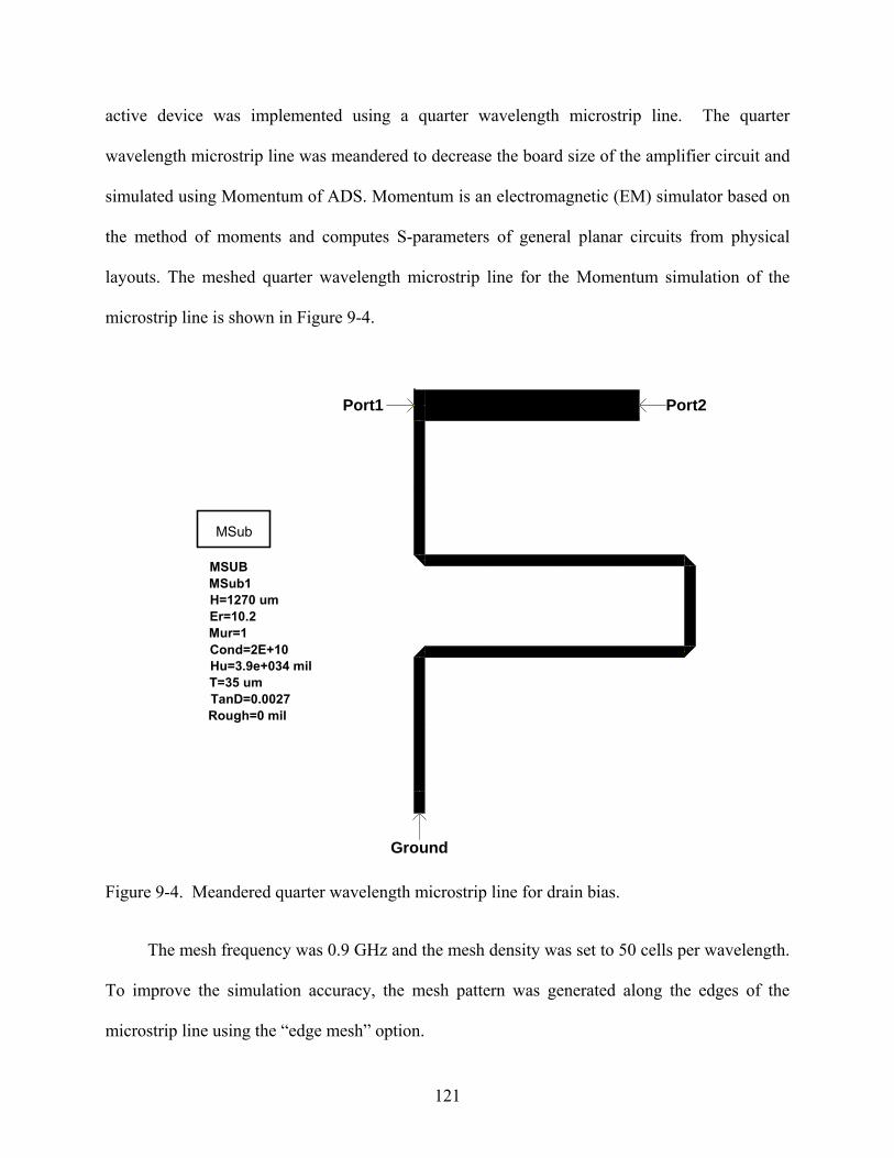
active device was implemented using a quarter wavelength microstrip line. The quarter
wavelength microstrip line was meandered to decrease the board size of the amplifier circuit and
simulated using Momentum of ADS. Momentum is an electromagnetic (EM) simulator based on
the method of moments and computes S-parameters of general planar circuits from physical
layouts. The meshed quarter wavelength microstrip line for the Momentum simulation of the
microstrip line is shown in Figure 9-4.
Port1 Port2
Ground
MSUBMSub1
Rough=0 milTanD=0.0027T=35 umHu=3.9e+034 milCond=2E+10Mur=1Er=10.2H=1270 um
MSub
Figure 9-4. Meandered quarter wavelength microstrip line for drain bias.
The mesh frequency was 0.9 GHz and the mesh density was set to 50 cells per wavelength.
To improve the simulation accuracy, the mesh pattern was generated along the edges of the
microstrip line using the “edge mesh” option.
121
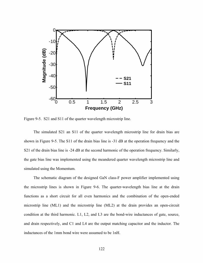
0 0.5 1 1.5 2 2.5 3-60
-50
-40
-30
-20
-10
0
Frequency (GHz)
Mag
nitu
de (d
B)
S21S11
Figure 9-5. S21 and S11 of the quarter wavelength microstrip line.
The simulated S21 an S11 of the quarter wavelength microstrip line for drain bias are
shown in Figure 9-5. The S11 of the drain bias line is -31 dB at the operation frequency and the
S21 of the drain bias line is -24 dB at the second harmonic of the operation frequency. Similarly,
the gate bias line was implemented using the meandered quarter wavelength microstrip line and
simulated using the Momentum.
The schematic diagram of the designed GaN class-F power amplifier implemented using
the microstrip lines is shown in Figure 9-6. The quarter-wavelength bias line at the drain
functions as a short circuit for all even harmonics and the combination of the open-ended
microstrip line (ML1) and the microstrip line (ML2) at the drain provides an open-circuit
condition at the third harmonic. L1, L2, and L3 are the bond-wire inductances of gate, source,
and drain respectively, and C1 and L4 are the output matching capacitor and the inductor. The
inductances of the 1mm bond wire were assumed to be 1nH.
122

L1
λ/4λ/4
VDD
Vout
Vin
VG
L2
L3
ML1
ML2
L4
C1
Figure 9-6. Designed class-F power amplifier.
When the bond wire inductance of the drain (L3) is ignored, the electrical length of the
transmission lines TL1 is one-sixth of π and that of TL2 is determined from the following
equation [83]:
⎟⎟⎠
⎞⎜⎜⎝
⎛⋅= −
outoo CZ ωθ
31tan
31 1 (7.3)
where Zo is the characteristic impedance of the transmission line, Cout is the output
capacitance of the transistor and ωo is the operating frequency of the amplifier.
When the class-F amplifier is fabricated as a hybrid integrated circuit, the parasitic
inductance from a bond wire exists at the drain port and the open-circuit condition at the drain
for the third harmonic can be satisfied by modifying equation (7.1) to the following :
⎟⎟⎠
⎞⎜⎜⎝
⎛−⋅= −
o
po
outoo ZL
CZω
ωθ
33
1tan31 1 (7.4)
123

where Lp is the parasitic inductance at the drain from a bond wire. However, the short-
circuit condition for all even harmonics can not be met and the performance of the class F
amplifier is adversely affected as the operating frequency increases.
0 0.5 1 1.5 20
5
10
15
20
25
0 0.5 1 1.5 2 0
0.03
0.06
0.09
0.12
Time (nano second)
Dra
in V
olta
ge (V
)
Dra
in C
urre
nt (A
)
Figure 9-7. Current and voltage wave form at the drain of the class F power amplifier.
Figure 9-7 shows the harmonic balance simulation of the voltage and the current waveform
at the drain port of the GaN HEMT. Under the designed harmonic load conditions, the voltage
shape and the current shape at the drain port approximate a square wave and a half sine wave
respectively.
9.4 Fabrication and Measurement
The GaN HEMT was mounted and wedge bond wired. The bond-wires and GaN HEMT
were encapsulated by the epoxy paste that was designed to protect devices during assembly and
handling. The 0603 size of Murata chip elements were used for the input and output matching
124
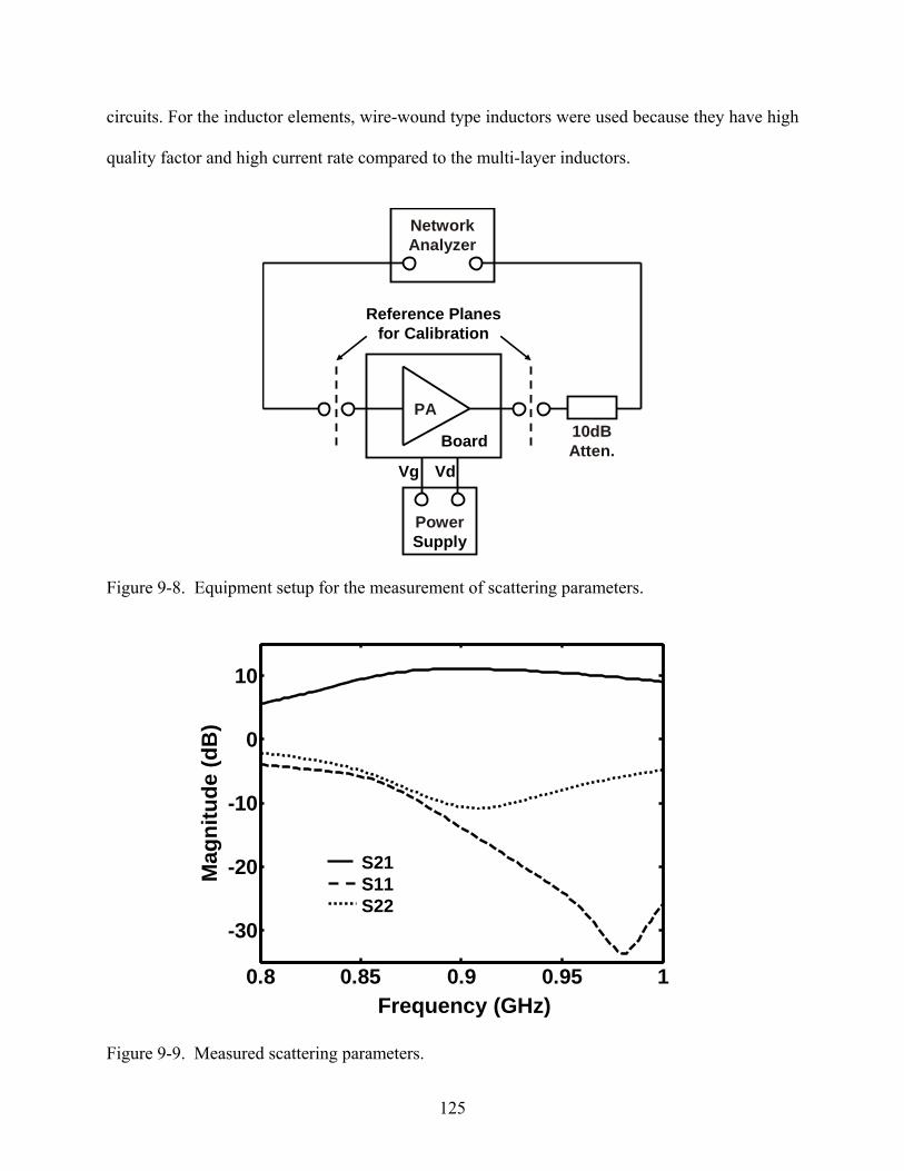
circuits. For the inductor elements, wire-wound type inductors were used because they have high
quality factor and high current rate compared to the multi-layer inductors.
PA
NetworkAnalyzer
Board 10dBAtten.
Vg Vd
Reference Planesfor Calibration
PowerSupply
Figure 9-8. Equipment setup for the measurement of scattering parameters.
0.8 0.85 0.9 0.95 1
-30
-20
-10
0
10
Frequency (GHz)
Mag
nitu
de (d
B)
S21S11S22
Figure 9-9. Measured scattering parameters.
125

The measurement set-up for the scattering parameter of the class F power amplifier is
shown in Figure 9-8. The input and the output scattering parameters are 14 dB and 10 dB,
respectively and the small signal gain of the class F power amplifier is 11 dB at 900 MHz
operating frequency.
0 5 10 150
5
10
15
20
25
30
0 5 10 15 0
10
20
30
40
Input Power (dBm)
Out
put P
ower
(dB
m),
Gai
n (d
B)
Power
PAE
(%)
PAE
Gain
Figure 9-10. Measured output power, gain, and PAE of the class F power amplifier.
The measured results of the output power and the PAE of the amplifier are shown in
Figure 9-10. The output saturated power was 25 dBm at the input power of 16 dBm. A maximum
PAE of 38 % was optimized at an output power of 24.5 dBm which is very close to the 1 dB
compression point of 24 dBm. This ensures that the power amplifier can operate at high
efficiency with good linearity when operating at a few dB back off from P1dB. The PAE can be
further improved if the knee voltage of the AlGaN/GaN HEMT is reduced. The size of the
126

fabricated class F power amplifier implemented using microstrip-lines and lumped elements is 5
cm by 4.5 cm.
Figure 9-11. Fabricated class F power amplifier.
127

CHAPTER 10 SUMMARY AND FUTURE WORK
10.1 Summary and Conclusion
This dissertation consists of two parts. The first part discusses the linearization of the
CMOS power amplifier with the integrated RF and analog linearization circuits. The second part
discusses the high efficiency operation of the power amplifier using wide bandgap device. This
chapter describes summary and future works for each of two subjects.
10.1.1 Summary on Linearization of CMOS Power Amplifier
Two kinds of predistorters were proposed for the CMOS power amplifier. The first type of
predistorter uses a diode-connected MOSFET as a nonlinearity generation circuit and the second
type of predistorter uses a MOSFET in near-cold FET condition as a nonlinearity generation
circuit. The equivalent elements of the proposed predistorters were extracted from the harmonic
balance large signal simulation. The amplitude and phase formula of the gains of the
predistorters were derived using the equivalent elements and the large signal gains were
simulated. On the other hand, the phase distortion characteristic of the cascode CMOS power
amplifier was investigated. The predistorters were integrated with CMOS power amplifiers and
the linearization performances of the CMOS power amplifiers with the predistorters were
simulated. For the experimental study, three power amplifiers were implemented using 0.18 µm
mixed-mode 1P6M UMC CMOS process and the on-chip probing was conducted for the
measurement. Small signal scattering parameters, output P1 dB, PAE, and IMD3 of the power
amplifier were measured. The measured IMD3 results were compared with the simulated IMD3
results with several bias voltages for the predistorters. The IMD3 measurement showed the
linearity improvement for three fabricated power amplifiers. In the case of the predistorter using
the diode-connected MOSFET, the IMD3 was improved over a certain output power range with
128
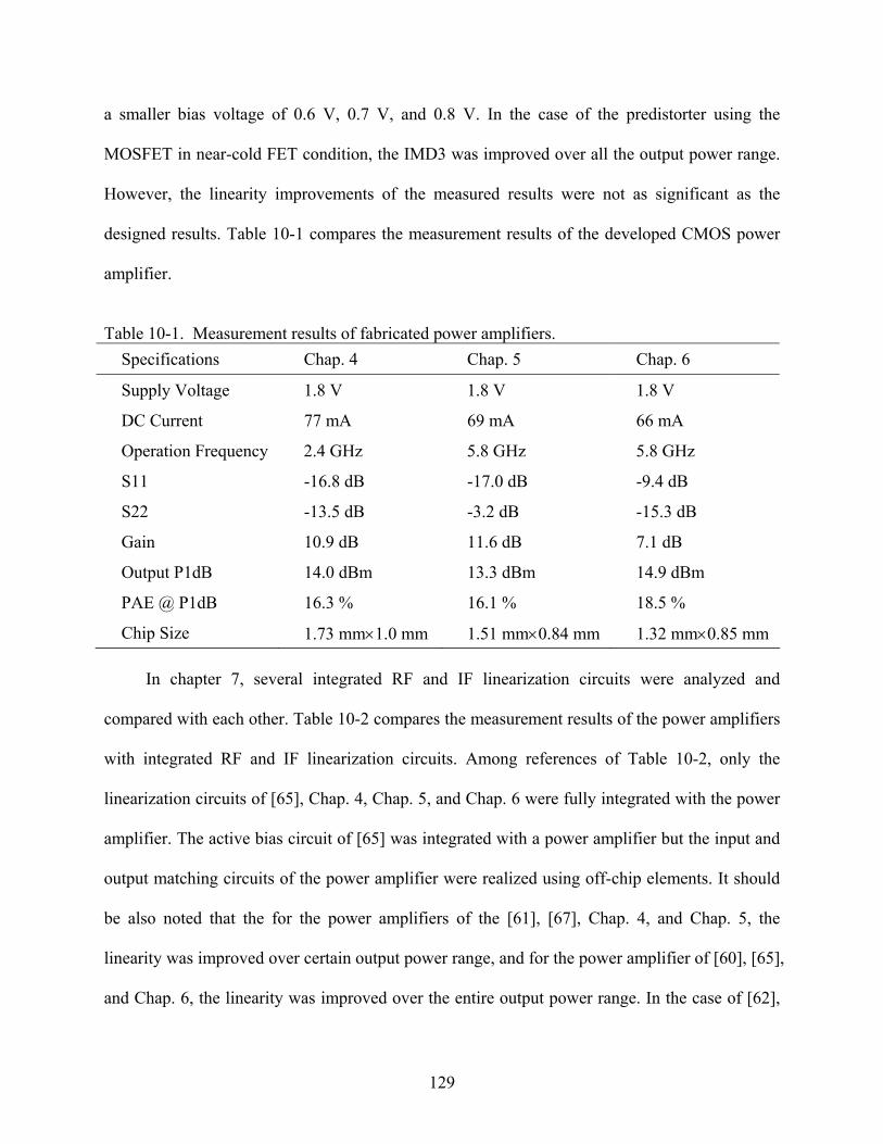
a smaller bias voltage of 0.6 V, 0.7 V, and 0.8 V. In the case of the predistorter using the
MOSFET in near-cold FET condition, the IMD3 was improved over all the output power range.
However, the linearity improvements of the measured results were not as significant as the
designed results. Table 10-1 compares the measurement results of the developed CMOS power
amplifier.
Table 10-1. Measurement results of fabricated power amplifiers.
Specifications Chap. 4 Chap. 5 Chap. 6
Supply Voltage 1.8 V 1.8 V 1.8 V
DC Current 77 mA 69 mA 66 mA
Operation Frequency 2.4 GHz 5.8 GHz 5.8 GHz
S11 -16.8 dB -17.0 dB -9.4 dB
S22 -13.5 dB -3.2 dB -15.3 dB
Gain 10.9 dB 11.6 dB 7.1 dB
Output P1dB 14.0 dBm 13.3 dBm 14.9 dBm
PAE @ P1dB 16.3 % 16.1 % 18.5 %
Chip Size 1.73 mm×1.0 mm 1.51 mm×0.84 mm 1.32 mm×0.85 mm
In chapter 7, several integrated RF and IF linearization circuits were analyzed and
compared with each other. Table 10-2 compares the measurement results of the power amplifiers
with integrated RF and IF linearization circuits. Among references of Table 10-2, only the
linearization circuits of [65], Chap. 4, Chap. 5, and Chap. 6 were fully integrated with the power
amplifier. The active bias circuit of [65] was integrated with a power amplifier but the input and
output matching circuits of the power amplifier were realized using off-chip elements. It should
be also noted that the for the power amplifiers of the [61], [67], Chap. 4, and Chap. 5, the
linearity was improved over certain output power range, and for the power amplifier of [60], [65],
and Chap. 6, the linearity was improved over the entire output power range. In the case of [62],
129

the output power range on which the linearity was improved is not available. In the case of [60],
the predistorter using the Schottky is described as “MMIC linearizer” and it is not certain which
kind of compound process was used for the fabrication of the predistorter.
Table 10-2. Integrated RF and IF linearization circuits. Reference Type Technology Frequency Linearity Improvement
[60] RF PD Compound Process 18 GHz 20 dB in IMD3 at 15 dBm
[61] RF PD GaAs HJFET 1.95 GHz 5.7 dBc in ACPR at 26.2 dBm
[62] IF PD 0.35 µm CMOS 200 MHz More than 30 dB in IMD3
[63] Bias Control GaAs HBT 1.9 GHz 6.5 dBc in ACPR at -7 dBm
[65] Bias Control 0.25 µm CMOS 2.4 GHz 5 dBc in ACPR at 6 dBm
Chap. 4 RF PD 0.18 µm CMOS 2.4 GHz 11.7 dB in IMD3 at 1.2 dBm
Chap. 5 RF PD 0.18 µm CMOS 5.8 GHz 10.2 dB in IMD3 at 2 dBm
Chap. 6 RF PD 0.18 µm CMOS 5.8 GHz 5.6 dB in IMD3 at -1 dBm 10.1.2 Summary on High Efficiency GaN Power Amplifier
The high efficiency operation of the GaN power amplifier was demonstrated using class F
configuration. The 0.75 µm gate length and 300 µm gate width AlGaN/GaN HEMT was
modeled with the modified Curtice model using IC-CAP device modeling software. The design
issue of the output matching network of the class F power amplifier was described. The
operation frequency of the power amplifier was 900 MHz and the bias voltage of the drain was
13 V. Microstrip lines were used for the realization of the class F configuration. The meandered
microstrip lines were simulated using Momentum in ADS and the class F operation of the power
amplifier was verified from the rectangular voltage waveform and half sinusoidal current
waveform at the drain of GaN device. The measurement results of the fabricated class F power
amplifier matched well with the simulated results. The measured small signal gain was 11 dB
130

and the output P1 dB was 24 dBm. The maximum PAE was 38 % at the output power of 24.5
dBm.
10.2 Implication for Future Work
10.2.1 Implication for Future Work on Linearization of CMOS Power Amplifier
Regarding the predistorter linearization technique for the power amplifier, the performance
of the predistorters depends on the modeling of the active and passive device. It is because the
predistorter linearization mechanism requires the heavily nonlinear operation of the active device.
The passive elements also affect the AM-PM characteristic of the predistorter. For the linearity
of the power amplifier to be significantly improved, the active and passive devices should be
precisely modeled. Besides that, the layouts of the power amplifier and the preditorter need to be
carefully considered. In practice, the modeling of the active device is a seriously challenging
issue and it is the fundamental limit of the predistorter circuit. On the other hand, the nonlinear
characteristics of the power amplifier vary with the temperature as well as the process variation.
In addition to it, the characteristic of the active device change with the aging. For the
linearization of the CMOS power amplifier, feedback linearization techniques can be sought.
Especially, the feedback technique in chapter 3 does not require the precise model of the active
device [84]. Besides the modeling issue, the feedback technique can deal with the temperature
variation and device aging issue.
10.2.2 Implication for Future Work on High Efficiency GaN Power Amplifier
The high efficiency operation of the GaN power amplifier was successfully demonstrated
in the dissertation. However, the experiment was conducted with the small area GaN device
which has the gate width of 300 µm and saturated drain current of 140 mA. Thus, the operational
drain current of the device was low and the drain bias voltage of the GaN device was limited to
13 V. The small drain current of the device also prevented the design of the class E power
131

amplifier. In order to employ the full capability of the wide bandgap device and to obtain high
output power and high efficiency, the large area device needs to be utilized. After the stability
issue of the currently available 2mm GaN device is resolved, the large output power with high
efficiency could be achieved with the large area device using the class E configuration.
132

LIST OF REFERENCES
[1] J. L. Dawson and T. H. Lee, “Cartesian feedback for RF power amplifier linearization,” Proc. American Control Conf., July 2004, pp. 361–366.
[2] F. H. Raab, B. E. Sigmon, R. G. Myers, and R. M. Jackson, “L-band transmitter using Kahn
EER technique,” IEEE Trans. Microwave Theory and Tech., vol. 46, pp. 2220-2225, Dec. 1998.
[3] A. Diet, C. Berland, M. Villegas, and G. Baudoin, “EER architecture specifications for
OFDM transmitter using a class E amplifier,” IEEE Microwave and Wireless Components Lett., vol. 14, pp. 389-391, Aug. 2004.
[4] T. Nesimoglu, K. A. Morris, S. C. Parker, and J. P. McGeehan, “Improved EER transmitters
for WLAN,” IEEE Radio and Wireless Symp., Jan. 2006, pp. 239-242. [5] G. Norris, R. Alford, J. Gehman, B. Gilsdorf, S. Hoggarth, G. Kurtzman, R. Meador, D.
Newman, D. Peckham, R. Sherman, J. Staudinger, G. Sadowniczak, and K. Traylor, “Optimized Closed Loop Polar GSM/GPRS/EDGE Transmitter,” IEEE MTT-S Int. Symp. Dig., June 2006, pp. 893-896.
[6] M. Ito, T. Yamawaki, M. Kasahara, and S. Williams, “Variable gain amplifier in polar loop
modulation transmitter for EDGE,” Proc. the 31st European Solid-State Circuits Conf., Sept. 2005, pp. 511-514.
[7] T. Sowlati, D. Rozenblit, R. Pullela, M. Damgaard, E. McCarthy, D. Koh, D. Ripley, F.
Balteanu, and I. Gheorghe, “Quad-Band GSM/GPRS/EDGE Polar Loop Transmitter,” IEEE J. Solid-State Circuits, vol. 39, no. 12, pp. 2179-2189, Dec. 2004.
[8] S. Pipilos, Y. Papananos, N. Naskas, M. Zervakis, J. Jongsma, T. Gschier, N. Wilson, J.
Gibbins, B. Carter, and G. Dann, “A transmitter IC for TETRA systems based on a Cartesian feedback loop linearization technique,” IEEE J. Solid-State Circuits, vol. 40, pp. 707–718, Mar. 2005.
[9] R. Bocock, P. R. Gray, E. Sacchi, L. Tee, and N. Wongkomet, “A Cartesian-Feedback
Linearized CMOS RF Transmitter for EDGE Modulation,” Symp. VLSI Circuits Digest of Technical Papers, 2006. pp. 232–233.
[10] R. J. Baker, CMOS circuit design, layout, and simulation, 2nd edition, IEEE Press,
Piscataway, NJ. 2005. [11] A. M. Niknejad and R. G. Meyer, Design, simulation and applications of inductors and
transformers for Si RF ICs, 2nd printing, Kluwer Academic Publishers, Norwell, MA. 2002. [12] V. Knopik, D. Gerna, D. Belot, M. Castagne, D. Gasquet, and L. Nativel, “Design and
analysis methodology for a Bluetooth sub-micron CMOS PA,” 27th European Solid-State Device Research Conf., pp. 421-424, Sep. 2001.
133

[13] K. Mertens and M. Steyart, “A fully integrated class 1 Bluetooth 0.25 µm CMOS PA,” 28th
European Solid-State Device Research Conf., pp. 219-222, Sep. 2002. [14] S. Sarkar, P. Sen, A. Raghavan, S. Chakarborty, and J. Laskar, “Development of 2.4 GHz
RF transceiver front-end chipset in 0.25 µm CMOS,” 16th Int. Conf. VLSI Design, pp. 42-47, Jan. 2003.
[15] R. Gilmore and L. Besser, Practical RF circuit design for modern wireless systems, volume
2, Artech House, Inc., Norwood, MA. 2003. [16] L. E. Larson, “Integrated circuit technology options for RFIC's-present status and future
directions,” Proc. IEEE Custom Integrated Circuits Conf., pp. 169–176, May. 1997. [17] Y. Ko, Design and optimization of 5 GHz CMOS power amplifiers with the differential
load-pull techniques, Ph.D thesis, Electrical and Computer Engineering Department, Univesity of Florida, 2005.
[18] R. J. Trew, “SiC and GaN transistors-Is there one winner for microwave power
applications?” Proc. IEEE, vol. 90, pp. 1032-1047, June 2002. [19] Yamanaka, K. Iyomasa, H. Ohtsuka, M. Nakayama, Y. Tsuyama, T. Kunii, Y. Kamo, and T.
Takagi, “S and C band over 100 W GaN HEMT 1-chip high power amplifiers with cell division configuration,” Gallium Arsenide and Other Semiconductor Application Symp, pp. 241–244, Oct. 2005.
[20] W. L. Pribble, J. W. Palmour, S. T. Sheppard, R. P. Smith, S. T. Allen, T. J. Smith, Z. Ring,
J. J. Sumakeris, A. W. Saxler, and J. W. Milligan “Applications of SiC MESFETs and GaN HEMTs in a power amplifier design,” IEEE MTT-S Int. Micowave Symp. Dig., vol. 3, pp. 1819-1822, June 2002.
[21] M. S. Shur, R. Gaska, A. Khan, and G. Simin, “Wide band gap electronic devices,” Devices,
Circuits and Syst., Proc. the 4th IEEE Int. Caracas Conf., pp. D051-1-D051-8, April 2002. [22] R. J. Trew, “Wide bandgap transistor amplifiers for improved performance microwave
power and radar applications,” IEEE Microwave Magazine, vol. 1, issue 1, pp. 46-54, Mar. 2000.
[23] M. S. Shur, A. D. Bykhovski, R. Gaska, and A. Khan, GaN-based Pyroelectronics and
Piezoelectronics, Handbook of Thin Film Devices, Volume 1: Hetero-structures for High Performance Devices, pp. 299-339, Academic Press, San Diego, CA. 2000.
[24] S. C. Cripps, RF Power Amplifiers for Wireless Communications, Artech House, Norwood,
MA. 1999.
134

[25] Y. Tang, L. Qian, and Y. Wang, “Optimized software implementation of a full-rate IEEE 802.11a compliant digital baseband transmitter on a digital signal processor,” IEEE Global Telecommunications Conf., vol. 4, issue 1, pp. 2194-2198, Dec. 2005.
[26] IEEE 802.11a-1999, “Wireless LAN medium access control (MAC) and physical layer
(PHY) specifications: High speed physical layer in the 5 GHz band,” 1999. [27] IEEE 802.11b-1999, “Wireless LAN medium access control (MAC) and physical layer
(PHY) specifications: High speed physical layer extension in the 2.4 GHz band,” 1999. [28] IEEE 802.11g-2003, “Wireless LAN medium access control (MAC) and physical layer
(PHY) specifications: Further higher data rate extension in the 2.4 GHz band,” 2003. [29] J. L. S, and A. E. W, “Safety evaluation of Bluetooth class ISM band transmitter on board
commercial aircraft,” Dec. 2000. [30] Y. S. Rao, W. Yeung, and A. Kripalani, “Third-generation (3G) radio access standards,”
Proc. Int. Conf. Communication Tech., vol. 2, pp. 1017-1023, Aug. 2003. [31] S. Y. Hui, and K. H. Yeung, “Challenges in the Migration to 4 G Mobile systems,” IEEE
Communications Magazine, vol. 41, pp. 54-59, Dec. 2003 [32] K. Hansen, “Wireless RF design challenges,” IEEE Radio Frequency Integrated Circuits
Symp., pp. 3-7, June 2003. [33] J. Crols and M. Steyaert, CMOS Wireless Transceiver Design, Kluwer Academic Publishers,
Norwell, MA. 1997. [34] V. Andrews et al., “A Monolithic Digital Chirp Synthesizer Chip with I and Q Channels,”
IEEE J. Solid State Circuits, vol. 27, no. 10, pp. 1321-1326, Oct. 1992. [35] B. Razavi, Microelectronics, 1st edition, Prentice-Hall, NJ. 1998. [36] B. Leung, VLSI for wireless communication, Prentice Hall, NJ. 2002. [37] P. B. Kenington, High Linearity RF Amplifier Design, Artech House, Norwood, MA. 2000. [38] N. B. Carvalho and J. C. Pedro, “Multi-tone intermodulation distortion performance of 3rd
order microwave circuits,” IEEE MTT-S Int. Microwave Symp. Dig., vol. 2, pp. 763–766, June 1999.
[39] D. Leenaerts, J. V. Tang, and C. Vaucher, Circuit design for RF transceiver, Kluwer
Academic Publishers, Norwell, MA. 2001. [40] W. J. Rugh, Nonlinear System and Theory: The Volterra/Wiener Approach, The Johns
Hopkins University Press, Baltimore, Maryland, 1981.
135

[41] M. Johansson, Linearization of RF power amplifiers using Cartesian feedback, Tech. Rep.,
Lund University, Thesis for the Degree of Teknisk Licentiat, 1991. [42] H. S. Black, “Stabilized feedback amplifiers,” Bell Syst. Tech. J., vol. 13, pp. 1-18, 1934. [43] L. Kahn, “Single sideband transmission by envelope elimination and restoration,” Proc. IRE,
vol. 40, pp. 803-806, July 1952 [44] S. Hietakangas, T. Rautio, and T. Rahkonen, “1 GHz Class E RF Power Amplifier for a
Polar Transmitter,” 24th Norchip Conference, Nov. 2006, pp. 5-9. [45] V. Petrovic and W. Gosling, “Polar-loop transmitter,” IEE Electronics Lett., vol. 15, no. 10,
pp. 286-288, May 1979. [46] L. W. Couch II, Digital and Analog Communication systems, Artech House, Norwood,
MA.1999. [47] P. Reynaert and M. Steyaert, RF Power Amplifiers for Mobile Communications, Springer,
Dordrecht, Netherlands, 2006. [48] Y. J. Chong, I. K. Lee, S. H. Oh, “Cartesian feedback loop chip for the narrow-band radio
system,” The 8th Int. Con. Communication Syst., Nov. 2002, pp. 1179-1184. [49] F. Carrara, A. Scuderi, and G. Palmisano, “Wide-bandwidth fully integrated Cartesian
feedback transmitter,” Proc. IEEE the Custom Integrated Circuits Conf., Sept. 2003, pp. 451-454.
[50] J. L. Dawson, and T. H. Lee, “Automatic phase alignment for a fully integrated Cartesian
feedback power amplifier system,” IEEE J. Solid-State Circuits, vol. 38, pp. 2269–2279, Dec. 2003.
[51] L. Perraud, M. Recouly, C. Pinatel, N. Sornin, J. L. Bonnot, F. Benoist, M. Massei, and
O.Gibrat, “A direct-conversion CMOS transceiver for the 802.11a/b/g WLAN standard utilizing a Cartesian feedback transmitter,” IEEE J. Solid-State Circuits, vol. 39, pp. 2226-2238, Dec. 2004
[52] S. C. Cripps, Advanced techniques in RF power amplifier design, Artech House, Norwood,
MA. 2002. [53] H. Hayashi, M. Nakatsugawa and M. Muraguchi, “Quasi-linear amplification using self
phase distortion compensation technique,” IEEE Trans. Microwave Theory and Tech., vol. 43, no. 11, pp. 2557-2564, Nov. 1995.
136

[54] Y. Y. Woo, J. Kim, J. Yi, S. Hong, I. Kim, J. Moon, and B. Kim, “Adaptive Digital Feedback Predistortion Technique for Linearizing Power Amplifiers,” IEEE Trans. Microwave Theory and Tech., vol. 55, pp. 932–940, May 2007.
[55] S. Kusunoki, K. Yamamoto, T. Hatsugai, H. Nagaoka, K. Tagami, N. Tominaga, K. Osawa,
K. Tanabe, S. Sakurai, and T. Iida, “Power-amplifier module with digital adaptive predistortion for cellular phones,” IEEE Trans. Microwave Theory and Tech., vol. 50, pp. 2979–2986, Dec. 2002.
[56] N. Ceylan, J. E. Mueller, and R. Weigel, “Optimization of EDGE terminal power amplifiers
using memoryless digital predistortion,” IEEE Trans. Microwave Theory and Tech., vol. 53, pp. 515-522, Feb. 2005.
[57] H. Seidel, “A Microwave Feedforward Experiment,” Bell Syst. Tech. J., vol. 50, pp. 2879-
2916, Nov. 1971. [58] N. Pothecary, Feed-forward Linear Power Amplifiers, Artech House, Norwood, MA. 1999. [59] P. Sen, V. Garg, R. Garg, N.B. Chakrabarti, “Design of power amplifiers at 2.4 GHz/900
MHz and implementation of on-chip linearization technique in 0.18/0.25/spl mu/m CMOS,” Proc.17th Int. Conf. VLSI Design, 2004 pp. 410-415.
[60] K. Yamauchi, M. Nakayama, Y. Ikeda, H. Nakaguro, N. Kadowaki, and T. Araki, “An 18
GHz-band MMIC linearizer using parallel diode with a bias feed resistance and a parallel capacitor,” IEEE Int. Microwave Symp. Dig., vol. 3, pp. 1507-1510, June 2000.
[61] G. Hau, T. B. Nishimura, and N. Iwata, “A highly efficient linearized wide-band CDMA
handset power amplifier based on predistortion under various bias condition,” IEEE Trans. Microwave Theory and Tech., vol. 49, no. 6, pp. 1194-1201, June 2001.
[62] E. Westesson and L. Sundstrom, “Low-power complex polynomial predistorter circuit in
CMOS for RF power amplifier linearization,” Proc. the 27th European Solid-State Circuit Conf., pp. 486-489, Sep. 2001.
[63] T. Yoshimasu, M. Akagi, N. Tanba, and S. Hara, “An HBT MMIC power amplifier with an
integrated diode linearizer for low-voltage potable phone applications,” IEEE J. Solid-Stage Circuits, vol. 33, no. 9, pp. 1290-1296, Sep. 1998.
[64] Y. S. Noh and C. S. Park, “PCS/W-CDMA dual-band MMIC power amplifier with a newly
proposed linearizing bias circuit,” IEEE J. Solid-Stage Circuits, vol. 37, no. 9, pp. 1096-1099, Sep. 2003.
[65] C. Yen and H. Chuang, “0.25-µm 20-dBm 2.4-GHz CMOS power amplifier with an
integrated diode linearizer,” IEEE Microwave and Wireless Components Lett., vol. 13, no. 2, Feb. 2003.
137

[66] T. H. Lee, The design of CMOS Radio Frequency Integrated Circuits, Cambridge University Press, New York, 1999.
[67] W. H. Chireix, “High Power Outphasing Modulation.” Proc. IRE, vol. 23, no. 11, pp. 1370-
1392, Nov. 1935. [68] J. L. B. Walker, High Power GaAs FET Amplifier, Artech House, Inc., Norwood, MA. 1993. [69] P. R. Gray, P. J. Hurst, S. H. Lewis, R. G. Meyer, Analysis and Design of Analog Integrated
Circuit, 4th edition, John Wiley, New York, 2001. [70] H. L. Kraus, C. W. Bostian, and F. H. Raab, Solid State Radio Engineering, John Wiley,
New York, 1980. [71] J. R. Smith, Modern Communication Circuits, 2nd edition, McGraw-Hill
Science/Engineering/Math, 1998. [72] M. Albulet, RF power amplifiers, Noble Publishing Corporation, Atlanta, GA. 2001. [73] N. O. Sokal and A. D. Sokal, “Class E, a new class of high-efficiency tuned single ended
switching power amplifier,” IEEE J. Solid Stage Circuit, vol. 10, pp. 168-176, June 1975. [74] M. M. Hella, M. Ismail, RF CMOS power amplifiers, theory, design and implementation,
Kluwer Academic Publishers, Norwell, MA. 2002. [75] C. J. Wei, P. DiCarlo, Y. A. Tkachenko, R. McMorrow, and D. Bartle, “Analysis and
experimental waveform study on inverse class-F mode of microwave power FETs,” IEEE MTT-S Int. Microwave Symp. Dig., vol. 1, pp. 525-528, June 2000.
[76] F. H. Raab, “Maximum efficiency and output of class F power amplifiers,” IEEE Trans.
Microwave Theory and Tech., vol. 49, pp. 1162-1166, June 2001. [77] Y. F. Wu, P. M. Chavarkar, M. Moore, P. Parikh, B. P. Keller, and U. K. Mishra, “A 50-W
AlGaN/GaN HEMT Amplifier,” Int. Electon Device Meeting, Technical Dig., pp. 375-376, Dec. 2000.
[78] S. Xie, V. Paidi, R. Coffie, S. Keller, S. Heikman, B. Moran, A. Chini, S. P. DenBarrs, U.
Mishra, S. Long, and M. J. W. Rodwell, “High Linearity Class B Power Amplifiers in GaN HEMT Technology,” IEEE Microwave and Wireless Components Lett., vol. 13, pp. 284-286, July 2003.
[79] V. Paidi, S. Xie, R. Coffie, B. Moran, S. Heikman, S. Keller, A. Chini, S. P. DenBaars, U. K.
Mishra, S. Long, and M. J. W. Rodwell, “High linearity and high efficiency of class B power amplifiers in GaN HEMT technology,” IEEE Trans. Microwave Theory and Tech., vol. 51, pp. 643-652, Feb. 2003.
138

[80] J. W. Lee, L. F. Eastman, and K. J. Webb, “A Gallium-Nitride Push-Pull Microwave Power Amplifier,” IEEE Trans. Microwave Theory and Tech., vol. 51, pp. 2243-2247, Nov. 2003.
[81] A. V. Grebennikov, “Circuit Design Technique for High Efficiency Class F Amplifiers,”
IEEE MTT-S Int. Microwave Symp. Dig., vol. 2, pp.771-774, June 2000. [82] W. R. Curtice, and M. Ettenberg, “A Nonlinear GaAs FET Model for Use in the Design of
Output Circuits for Power Amplifier,” IEEE Trans. Microwave Theory Tech., pp. 1383-1394, Dec. 1985.
[83] F. H. Raab, “Class F Power Amplifiers with Maximally Flat Waveforms,” IEEE Trans.
Microwave Theory and Tech., vol. 45, pp. 2007-2012, Nov. 1997. [84] J. L. Dawson and T. H. Lee, Feedback Linearization of RF Power Amplifiers, Kluwer
Academic Publishers, Norwell, MA. 2004.
139

BIOGRAPHICAL SKETCH
Sangwon Ko received a BS degree in electrical engineering from Hongik University,
Korea, in 1998 and a MS degree in electrical and computer engineering from University of
Florida in 2004. During his MS program, he studied RF power amplifier and oscillator circuits.
Since July 2003, he has been working on RFSOC group at University of Florida. His
research interests involve microwave and RF circuit design specializing in high frequency power
amplifier and high frequency device modeling.
140


![[Book] CMOS Current Amplifiers](https://img.pdfslide.us/doc/110x75/54e62e884a7959e23f8b47cb/book-cmos-current-amplifiers.jpg)