Embed Size (px)
Citation preview
Module 2
DC Circuit
Version 2 EE IIT, Kharagpur
Lesson 3
Introduction of Electric Circuit
Version 2 EE IIT, Kharagpur
Objectives • Familiarity with and understanding of the basic elements encountered in electric
networks. • To learn the fundamental differences between linear and nonlinear circuits. • To understand the Kirchhoff’s voltage and current laws and their applications to
circuits. • Meaning of circuit ground and the voltages referenced to ground. • Understanding the basic principles of voltage dividers and current dividers. • Potentiometer and loading effects. • To understand the fundamental differences between ideal and practical voltage
and current sources and their mathematical models to represent these source models in electric circuits.
• Distinguish between independent and dependent sources those encountered in electric circuits.
• Meaning of delivering and absorbing power by the source.
L.3.1 Introduction The interconnection of various electric elements in a prescribed manner comprises as an electric circuit in order to perform a desired function. The electric elements include controlled and uncontrolled source of energy, resistors, capacitors, inductors, etc. Analysis of electric circuits refers to computations required to determine the unknown quantities such as voltage, current and power associated with one or more elements in the circuit. To contribute to the solution of engineering problems one must acquire the basic knowledge of electric circuit analysis and laws. Many other systems, like mechanical, hydraulic, thermal, magnetic and power system are easy to analyze and model by a circuit. To learn how to analyze the models of these systems, first one needs to learn the techniques of circuit analysis. We shall discuss briefly some of the basic circuit elements and the laws that will help us to develop the background of subject.
L-3.1.1 Basic Elements & Introductory Concepts Electrical Network: A combination of various electric elements (Resistor, Inductor, Capacitor, Voltage source, Current source) connected in any manner what so ever is called an electrical network. We may classify circuit elements in two categories, passive and active elements. Passive Element: The element which receives energy (or absorbs energy) and then either converts it into heat (R) or stored it in an electric (C) or magnetic (L ) field is called passive element. Active Element: The elements that supply energy to the circuit is called active element. Examples of active elements include voltage and current sources, generators, and electronic devices that require power supplies. A transistor is an active circuit element, meaning that it can amplify power of a signal. On the other hand, transformer is not an active element because it does not amplify the power level and power remains same both
Version 2 EE IIT, Kharagpur
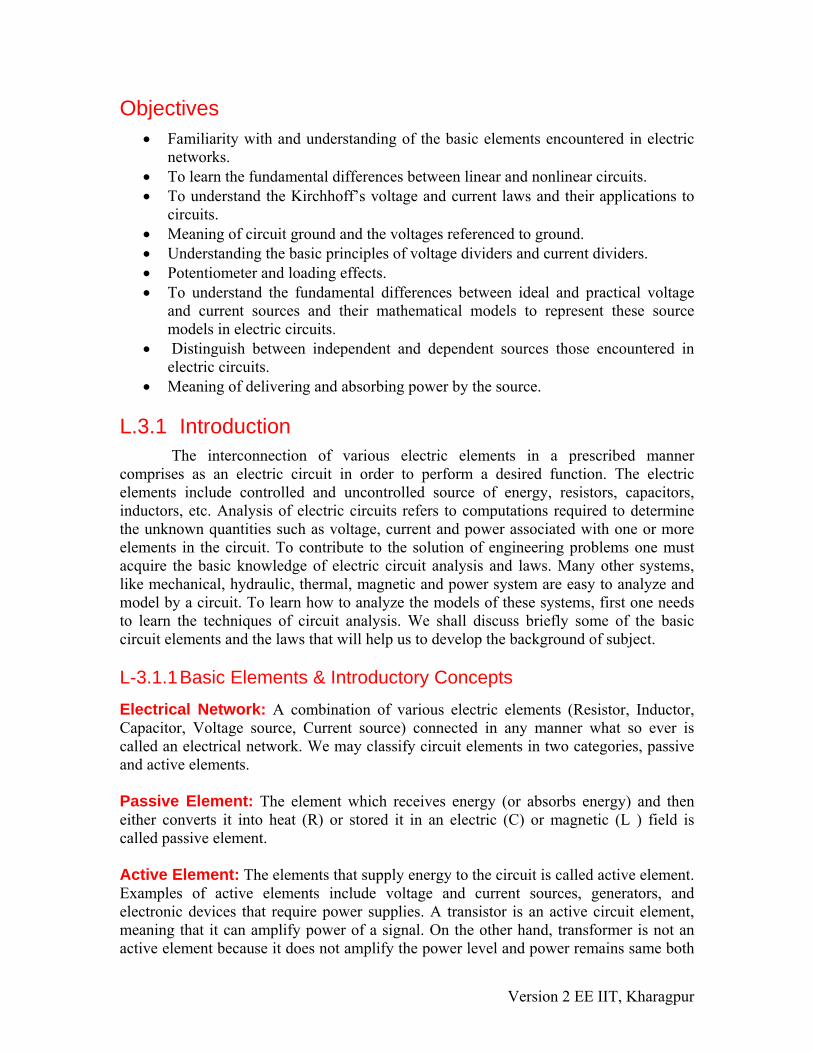
in primary and secondary sides. Transformer is an example of passive element. Bilateral Element: Conduction of current in both directions in an element (example: Resistance; Inductance; Capacitance) with same magnitude is termed as bilateral element.
Unilateral Element: Conduction of current in one direction is termed as unilateral (example: Diode, Transistor) element.
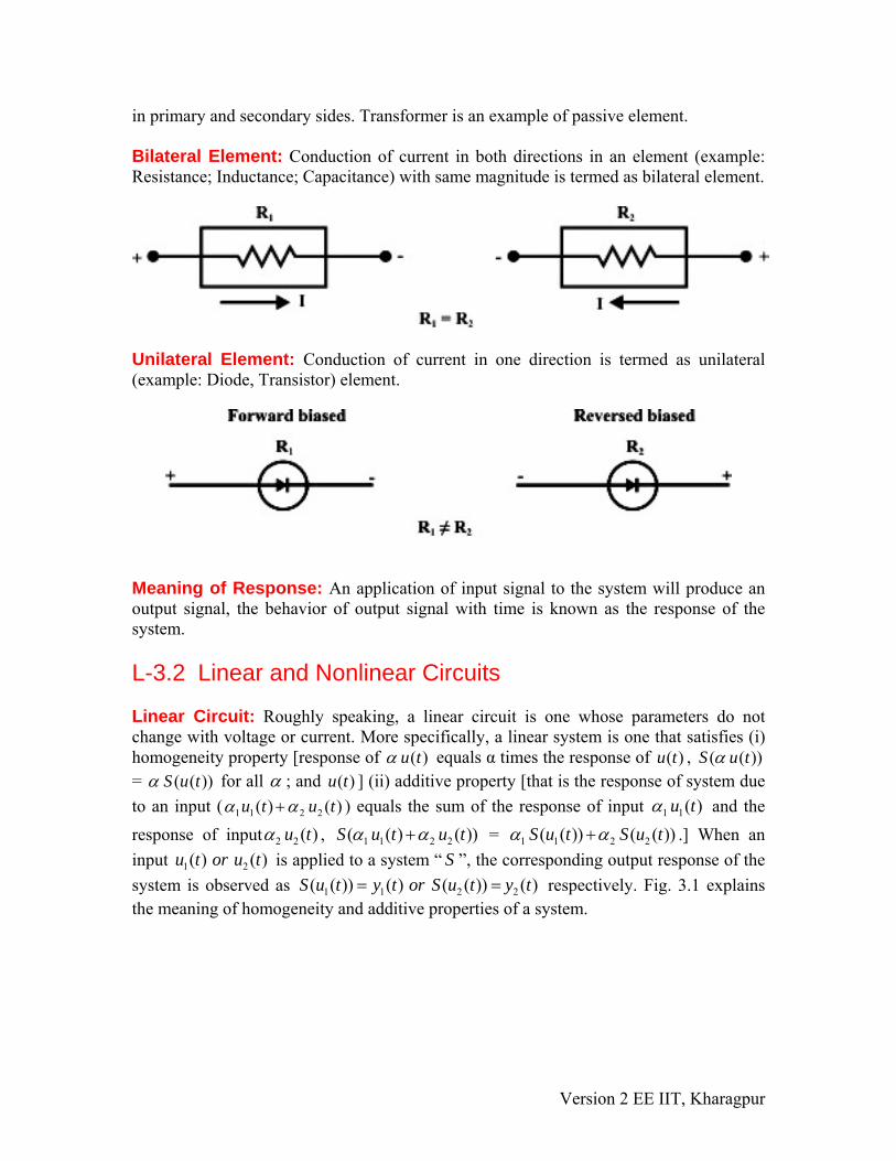
Meaning of Response: An application of input signal to the system will produce an output signal, the behavior of output signal with time is known as the response of the system. L-3.2 Linear and Nonlinear Circuits Linear Circuit: Roughly speaking, a linear circuit is one whose parameters do not change with voltage or current. More specifically, a linear system is one that satisfies (i) homogeneity property [response of ( )u tα equals α times the response of , ( )u t ( ( )S u t )α = ( ( ))S u tα for all α ; and ] (ii) additive property [that is the response of system due to an input (
( )u t
1 1 2 2( ) ( )u t u tα α+ ) equals the sum of the response of input 1 1( )u tα and the response of input 2 2 ( )u tα , 1 1 2 2( ( ) (S u t u t))α α+ = 1 1 2 2( ( )) ( ( ))S u t S u tα α+ .] When an input is applied to a system “ ”, the corresponding output response of the system is observed as respectively. Fig. 3.1 explains the meaning of homogeneity and additive properties of a system.
1 2( ) ( )u t or u t S
1 1 2 2( ( )) ( ) ( ( )) ( )S u t y t or S u t y t= =
Version 2 EE IIT, Kharagpur
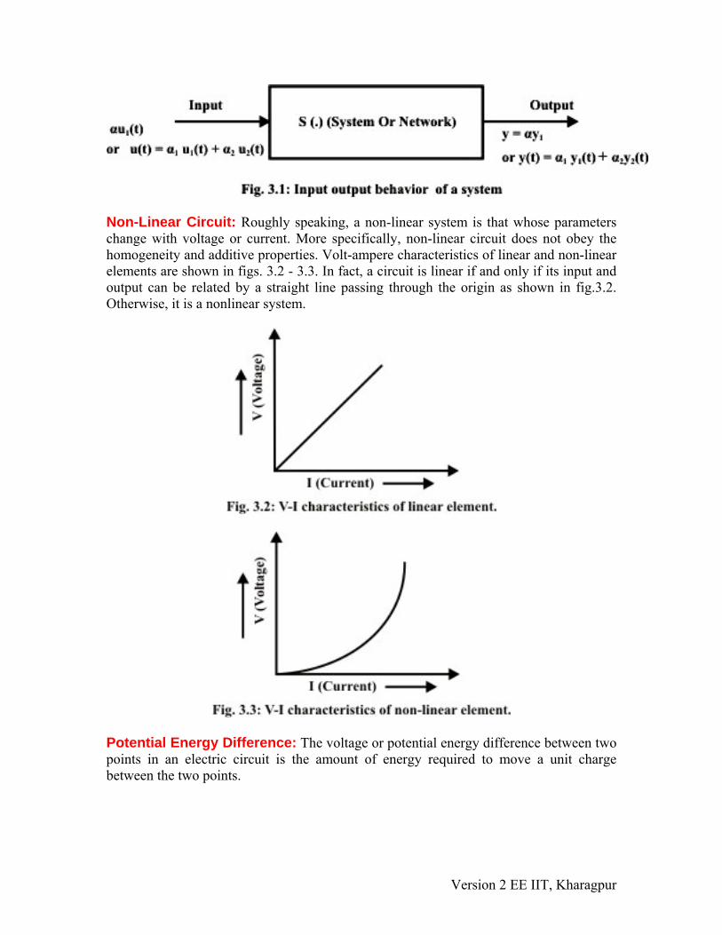
Non-Linear Circuit: Roughly speaking, a non-linear system is that whose parameters change with voltage or current. More specifically, non-linear circuit does not obey the homogeneity and additive properties. Volt-ampere characteristics of linear and non-linear elements are shown in figs. 3.2 - 3.3. In fact, a circuit is linear if and only if its input and output can be related by a straight line passing through the origin as shown in fig.3.2. Otherwise, it is a nonlinear system.
Potential Energy Difference: The voltage or potential energy difference between two points in an electric circuit is the amount of energy required to move a unit charge between the two points.
Version 2 EE IIT, Kharagpur
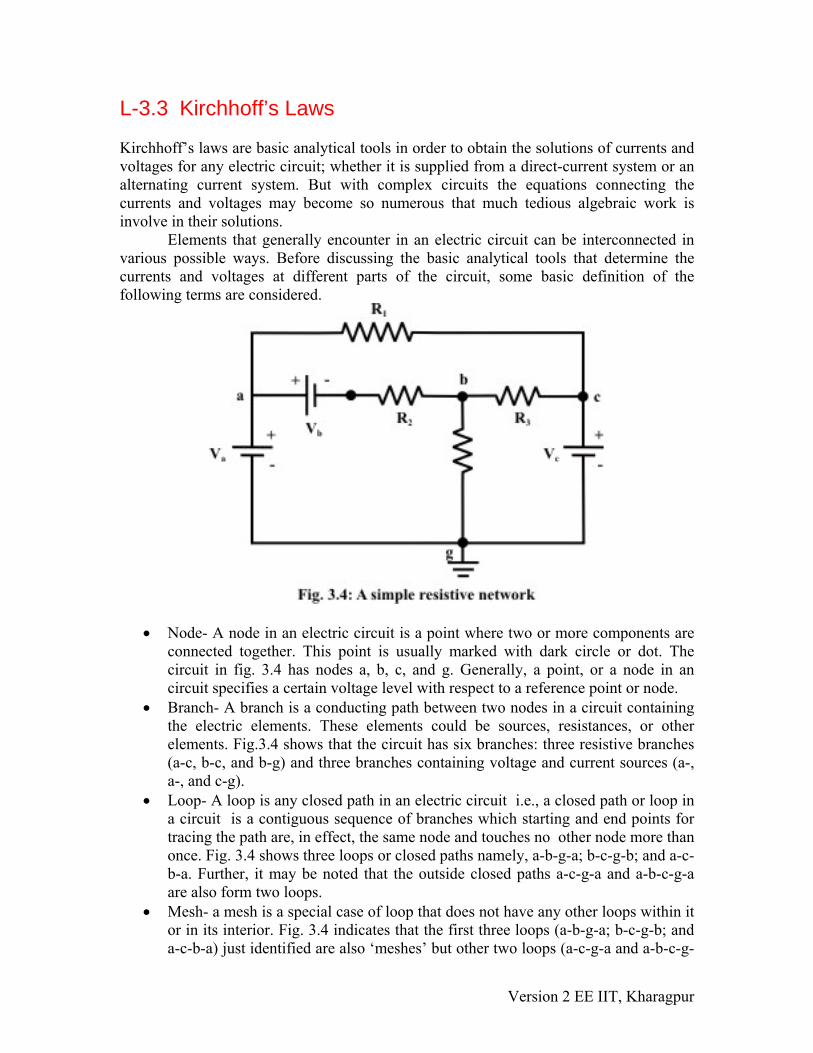
L-3.3 Kirchhoff’s Laws Kirchhoff’s laws are basic analytical tools in order to obtain the solutions of currents and voltages for any electric circuit; whether it is supplied from a direct-current system or an alternating current system. But with complex circuits the equations connecting the currents and voltages may become so numerous that much tedious algebraic work is involve in their solutions. Elements that generally encounter in an electric circuit can be interconnected in various possible ways. Before discussing the basic analytical tools that determine the currents and voltages at different parts of the circuit, some basic definition of the following terms are considered.
• Node- A node in an electric circuit is a point where two or more components are connected together. This point is usually marked with dark circle or dot. The circuit in fig. 3.4 has nodes a, b, c, and g. Generally, a point, or a node in an circuit specifies a certain voltage level with respect to a reference point or node.
• Branch- A branch is a conducting path between two nodes in a circuit containing the electric elements. These elements could be sources, resistances, or other elements. Fig.3.4 shows that the circuit has six branches: three resistive branches (a-c, b-c, and b-g) and three branches containing voltage and current sources (a-, a-, and c-g).
• Loop- A loop is any closed path in an electric circuit i.e., a closed path or loop in a circuit is a contiguous sequence of branches which starting and end points for tracing the path are, in effect, the same node and touches no other node more than once. Fig. 3.4 shows three loops or closed paths namely, a-b-g-a; b-c-g-b; and a-c-b-a. Further, it may be noted that the outside closed paths a-c-g-a and a-b-c-g-a are also form two loops.
• Mesh- a mesh is a special case of loop that does not have any other loops within it or in its interior. Fig. 3.4 indicates that the first three loops (a-b-g-a; b-c-g-b; and a-c-b-a) just identified are also ‘meshes’ but other two loops (a-c-g-a and a-b-c-g-
Version 2 EE IIT, Kharagpur
a) are not. With the introduction of the Kirchhoff’s laws, a various types of electric circuits can be analyzed.
Version 2 EE IIT, Kharagpur
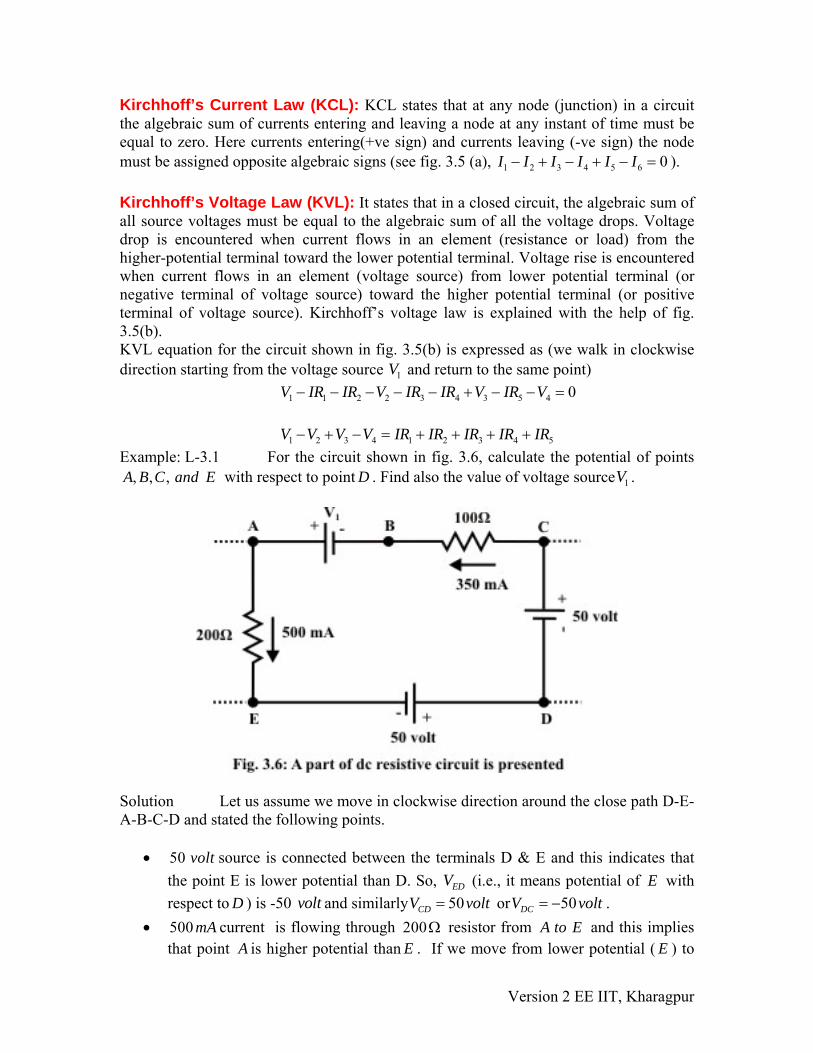
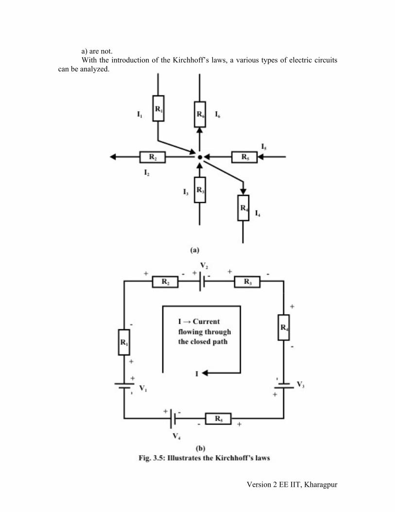
Kirchhoff’s Current Law (KCL): KCL states that at any node (junction) in a circuit the algebraic sum of currents entering and leaving a node at any instant of time must be equal to zero. Here currents entering(+ve sign) and currents leaving (-ve sign) the node must be assigned opposite algebraic signs (see fig. 3.5 (a), 1 2 3 4 5 6 0I I I I I I− + − + − = ). Kirchhoff’s Voltage Law (KVL): It states that in a closed circuit, the algebraic sum of all source voltages must be equal to the algebraic sum of all the voltage drops. Voltage drop is encountered when current flows in an element (resistance or load) from the higher-potential terminal toward the lower potential terminal. Voltage rise is encountered when current flows in an element (voltage source) from lower potential terminal (or negative terminal of voltage source) toward the higher potential terminal (or positive terminal of voltage source). Kirchhoff’s voltage law is explained with the help of fig. 3.5(b). KVL equation for the circuit shown in fig. 3.5(b) is expressed as (we walk in clockwise direction starting from the voltage source and return to the same point) 1V 1 1 2 2 3 4 3 5 4 0V IR IR V IR IR V IR V− − − − − + − − = 1 2 3 4 1 2 3 4 5V V V V IR IR IR IR IR− + − = + + + +Example: L-3.1 For the circuit shown in fig. 3.6, calculate the potential of points
, , ,A B C and E with respect to point . Find also the value of voltage source . D 1V
Solution Let us assume we move in clockwise direction around the close path D-E-A-B-C-D and stated the following points.
• source is connected between the terminals D & E and this indicates that the point E is lower potential than D. So, 50 volt
EDV (i.e., it means potential of E with respect to ) is -50 vo and similarlyD lt 50CDV volt= or 50DCV volt= − .
• current is flowing through 200500 mA Ω resistor from A to E and this implies that point A is higher potential than E . If we move from lower potential ( E ) to
Version 2 EE IIT, Kharagpur
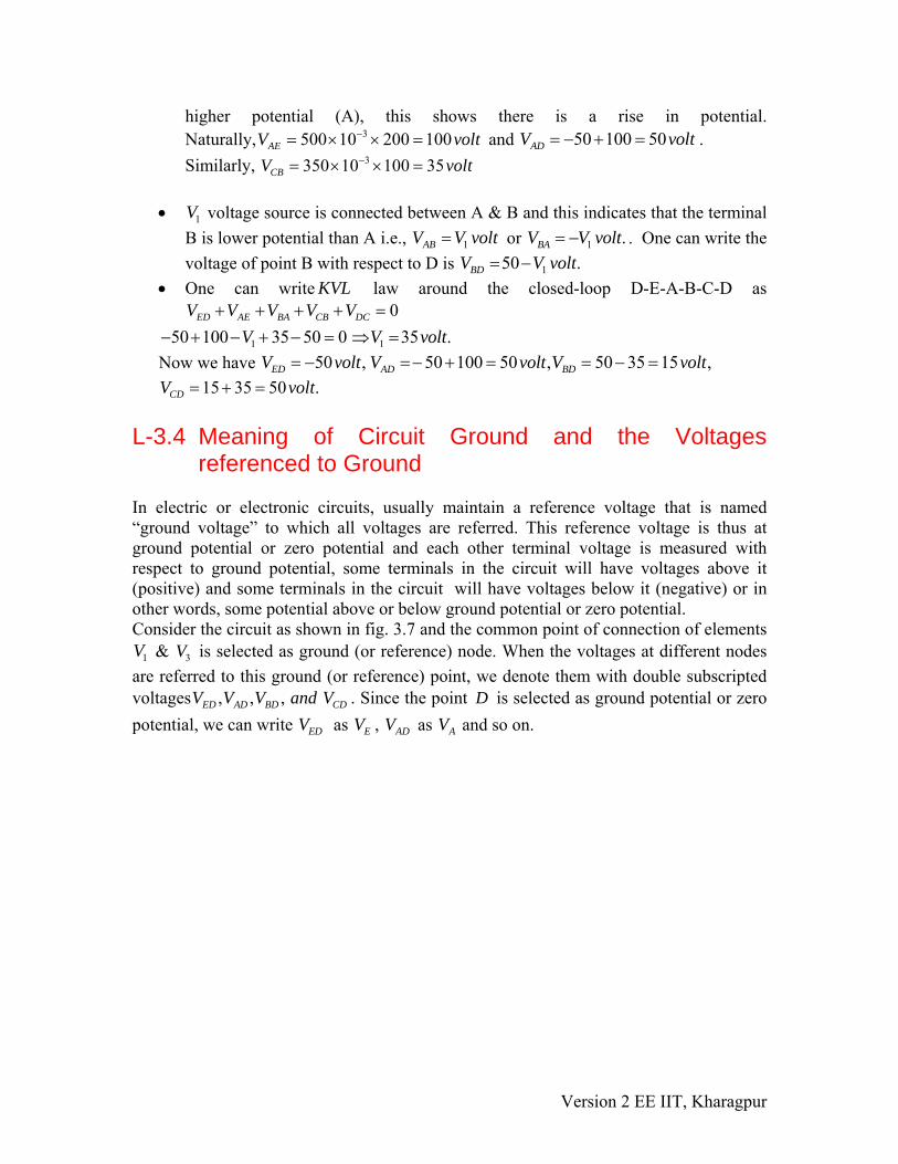
higher potential (A), this shows there is a rise in potential. Naturally, and 3500 10 200 100AEV volt−= × × = 50 100 50ADV volt= − + = . Similarly, 3350 10 100 35CBV v−= × × = olt
t
• voltage source is connected between A & B and this indicates that the terminal
B is lower potential than A i.e., 1V
1ABV V vol= or 1 .BAV V volt= − . One can write the voltage of point B with respect to D is 150 .BDV V volt= −
• One can write law around the closed-loop D-E-A-B-C-D as
KVL0ED AE BA CB DCV V V V V+ + + + =
1 150 100 35 50 0 35 .V V− + − + − = ⇒ = volt Now we have
50 , 50 100 50 , 50 35 15 ,ED AD BDV volt V volt V volt= − =− + = = − =
15 35 50 .CDV volt= + =
L-3.4 Meaning of Circuit Ground and the Voltages referenced to Ground
In electric or electronic circuits, usually maintain a reference voltage that is named “ground voltage” to which all voltages are referred. This reference voltage is thus at ground potential or zero potential and each other terminal voltage is measured with respect to ground potential, some terminals in the circuit will have voltages above it (positive) and some terminals in the circuit will have voltages below it (negative) or in other words, some potential above or below ground potential or zero potential. Consider the circuit as shown in fig. 3.7 and the common point of connection of elements
& is selected as ground (or reference) node. When the voltages at different nodes are referred to this ground (or reference) point, we denote them with double subscripted voltages . Since the point is selected as ground potential or zero potential, we can write
1V 3V
, , ,ED AD BD CDV V V and V D
EDV as EV , as and so on. ADV AV
Version 2 EE IIT, Kharagpur
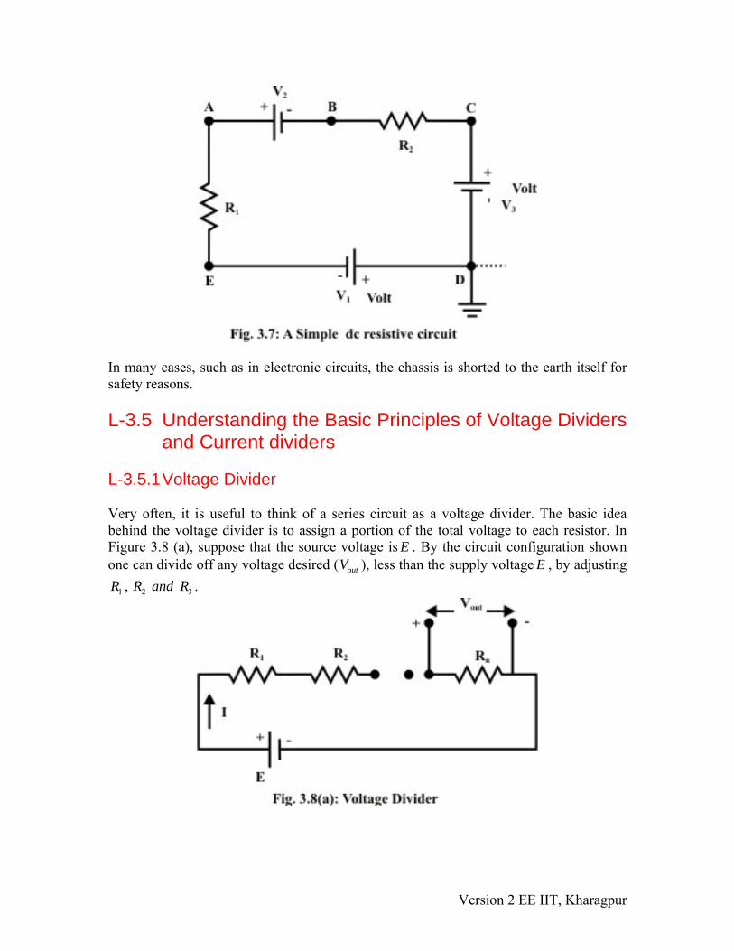
In many cases, such as in electronic circuits, the chassis is shorted to the earth itself for safety reasons. L-3.5 Understanding the Basic Principles of Voltage Dividers
and Current dividers L-3.5.1 Voltage Divider Very often, it is useful to think of a series circuit as a voltage divider. The basic idea behind the voltage divider is to assign a portion of the total voltage to each resistor. In Figure 3.8 (a), suppose that the source voltage is E . By the circuit configuration shown one can divide off any voltage desired ( ), less than the supply voltageoutV E , by adjusting
1 2, 3R R and R .
Version 2 EE IIT, Kharagpur
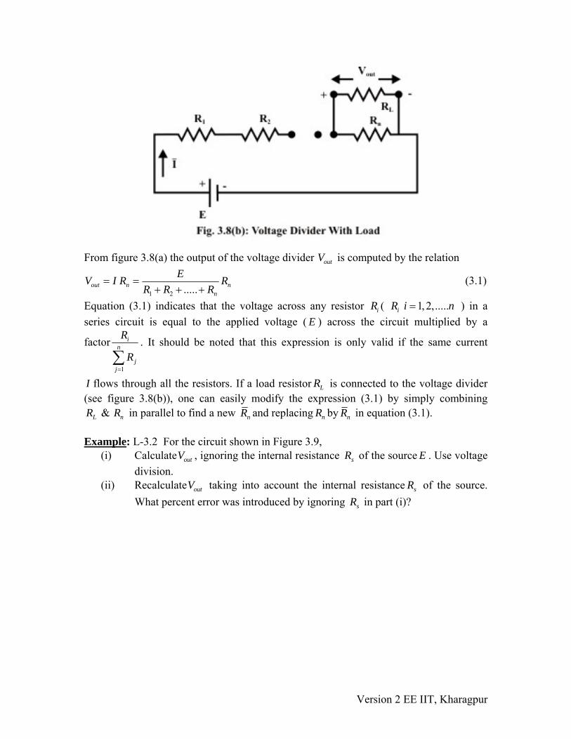
From figure 3.8(a) the output of the voltage divider is computed by the relation outV
1 2 .....out n nn
EV I R RR R R
= =+ + +
(3.1)
Equation (3.1) indicates that the voltage across any resistor iR ( 1, 2,.....iR i n= ) in a series circuit is equal to the applied voltage ( E ) across the circuit multiplied by a
factor
1
in
jj
R
R=∑
. It should be noted that this expression is only valid if the same current
I flows through all the resistors. If a load resistor is connected to the voltage divider (see figure 3.8(b)), one can easily modify the expression (3.1) by simply combining
LR
&L nR R in parallel to find a new nR and replacing nR by nR in equation (3.1). Example: L-3.2 For the circuit shown in Figure 3.9,
(i) Calculate , ignoring the internal resistance outV sR of the source E . Use voltage division.
(ii) Recalculate taking into account the internal resistanceoutV sR of the source. What percent error was introduced by ignoring sR in part (i)?
Version 2 EE IIT, Kharagpur
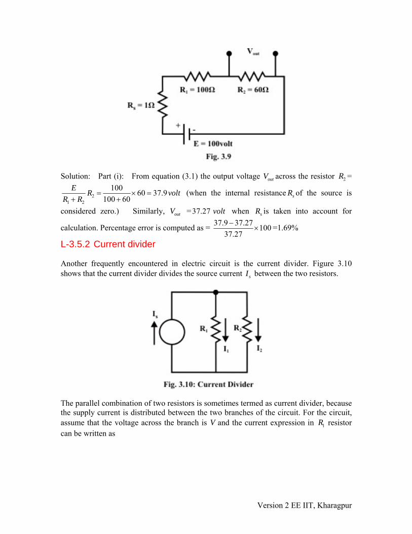
Solution: Part (i): From equation (3.1) the output voltage across the resistor = outV 2R
21 2
100 60 37.9100 60
E R voltR R
= × =+ +
(when the internal resistance sR of the source is
considered zero.) Similarly, =37 when outV .27 volt sR is taken into account for
calculation. Percentage error is computed as = 37.9 37.27 10037.27−
× =1.69%
L-3.5.2 Current divider Another frequently encountered in electric circuit is the current divider. Figure 3.10 shows that the current divider divides the source current sI between the two resistors.
The parallel combination of two resistors is sometimes termed as current divider, because the supply current is distributed between the two branches of the circuit. For the circuit, assume that the voltage across the branch is V and the current expression in resistor can be written as
1R
Version 2 EE IIT, Kharagpur
1 211
1 2 1 2
1 2
1 12
ss
VI RR or I II R R R
VR R
= = =+ +⎛ ⎞
+⎜ ⎟⎝ ⎠
RR
× . Similarly, the current flowing through
the can be obtained as 2R 12
1 2s
RI IR R
=+
× . It can be noted that the expression for 1I has
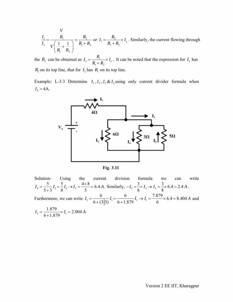
on its top line, that for 2R 2I has on its top line. 1R Example: L-3.3 Determine 1 2 3 5, , &I I I I using only current divider formula when
4I = 4A.
Solution- Using the current division formula we can write
4 3 3 35 5 4 8 6.4
5 3 8 5I I I I ×= = → = =
+A . Similarly, 5 3 5
3 3 6.4 2.48 8
I I I− = × → = × = A .
Furthermore, we can write 3 1 1 16 6 7.879 6.4 8.404
6 (3 5) 6 1.879 6I I I I= = → = × =
+ +A and
2 11.879 2.004 .
6 1.879I I A= × =
+
Version 2 EE IIT, Kharagpur
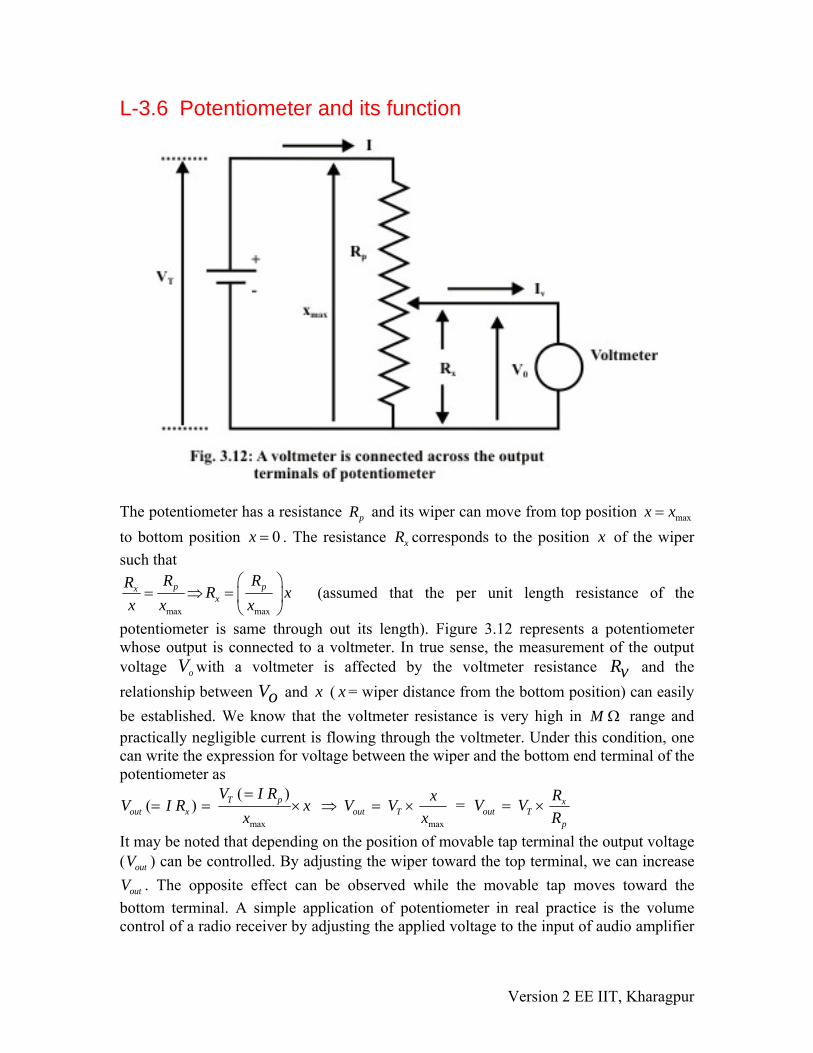
L-3.6 Potentiometer and its function
The potentiometer has a resistance pR and its wiper can move from top position maxx x= to bottom position . The resistance 0x = xR corresponds to the position x of the wiper such that
max max
pxx
R RR pR xx x x
⎛ ⎞= ⇒ = ⎜ ⎟
⎝ ⎠ (assumed that the per unit length resistance of the
potentiometer is same through out its length). Figure 3.12 represents a potentiometer whose output is connected to a voltmeter. In true sense, the measurement of the output voltage with a voltmeter is affected by the voltmeter resistance and the relationship between V and
oV Rvo x ( x = wiper distance from the bottom position) can easily
be established. We know that the voltmeter resistance is very high in range and practically negligible current is flowing through the voltmeter. Under this condition, one can write the expression for voltage between the wiper and the bottom end terminal of the potentiometer as
M Ω
max max
( )( ) T p
out x out T
V I R xV I R x V Vx x=
= = × ⇒ = × = xout T
p
RV VR
= ×
It may be noted that depending on the position of movable tap terminal the output voltage ( ) can be controlled. By adjusting the wiper toward the top terminal, we can increase
. The opposite effect can be observed while the movable tap moves toward the bottom terminal. A simple application of potentiometer in real practice is the volume control of a radio receiver by adjusting the applied voltage to the input of audio amplifier
outV
outV
Version 2 EE IIT, Kharagpur
of a radio set. This audio amplifier boosts this voltage by a certain fixed factor and this voltage is capable of driving the loudspeaker. Example- L-3.4 A potentiometer has 110 V applied across it. Adjust the position of
500 k− ΩbotR such that 47.5 V appears between the movable tap and the bottom end
terminal (refer fig.3.12). Solution- Since the output voltage ( ) is not connected to any load, in turn, we can write the following expression
botV
maxout T
xV Vx
= ×47.5 500000 216 .110
bot bot botbot T
T T T
V R VR R kV R V
= → = × = × = − Ω
L-3.7 Practical Voltage and Current Sources L-3.7.1 Ideal and Practical Voltage Sources
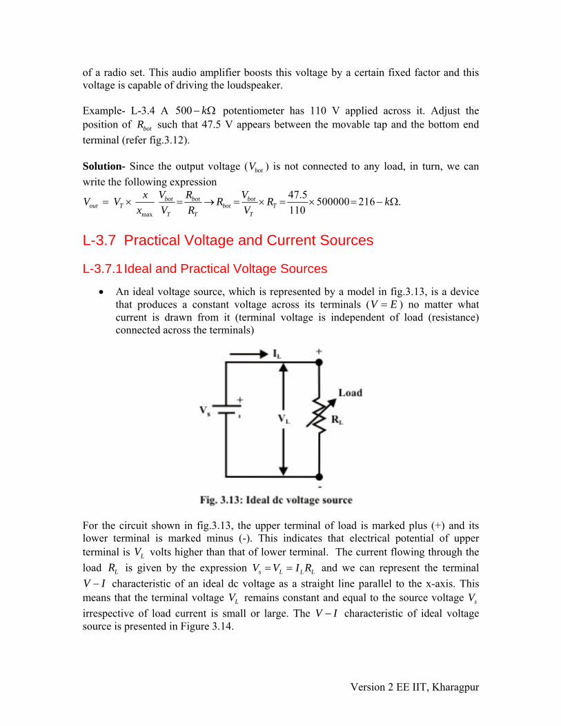
• An ideal voltage source, which is represented by a model in fig.3.13, is a device that produces a constant voltage across its terminals (V E= ) no matter what current is drawn from it (terminal voltage is independent of load (resistance) connected across the terminals)
For the circuit shown in fig.3.13, the upper terminal of load is marked plus (+) and its lower terminal is marked minus (-). This indicates that electrical potential of upper terminal is volts higher than that of lower terminal. The current flowing through the load is given by the expression
LV
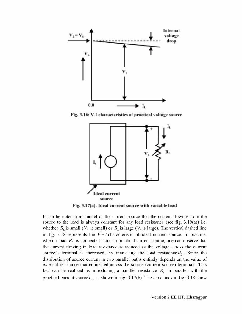
LR s L LV V I RL= = and we can represent the terminal characteristic of an ideal dc voltage as a straight line parallel to the x-axis. This
means that the terminal voltage remains constant and equal to the source voltage V I−
LV sV irrespective of load current is small or large. The V I− characteristic of ideal voltage source is presented in Figure 3.14.
Version 2 EE IIT, Kharagpur
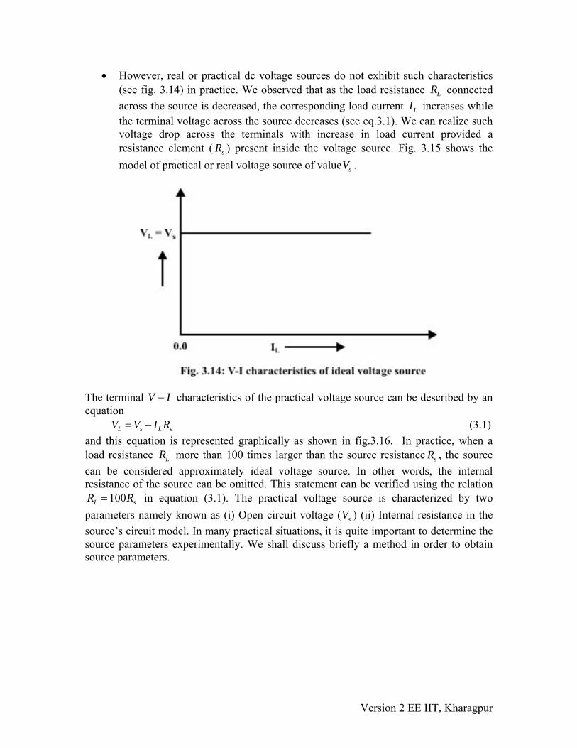
• However, real or practical dc voltage sources do not exhibit such characteristics (see fig. 3.14) in practice. We observed that as the load resistance connected across the source is decreased, the corresponding load current
LR
LI increases while the terminal voltage across the source decreases (see eq.3.1). We can realize such voltage drop across the terminals with increase in load current provided a resistance element ( sR ) present inside the voltage source. Fig. 3.15 shows the model of practical or real voltage source of value sV .
The terminal V characteristics of the practical voltage source can be described by an equation
I−
(3.1) L s LV V I R= − s
and this equation is represented graphically as shown in fig.3.16. In practice, when a load resistance more than 100 times larger than the source resistanceLR sR , the source can be considered approximately ideal voltage source. In other words, the internal resistance of the source can be omitted. This statement can be verified using the relation
100L sR R= in equation (3.1). The practical voltage source is characterized by two parameters namely known as (i) Open circuit voltage ( sV ) (ii) Internal resistance in the source’s circuit model. In many practical situations, it is quite important to determine the source parameters experimentally. We shall discuss briefly a method in order to obtain source parameters.
Version 2 EE IIT, Kharagpur
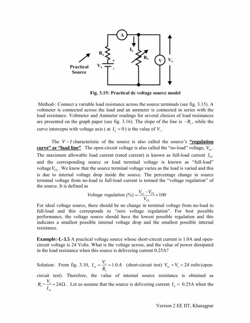
Method-: Connect a variable load resistance across the source terminals (see fig. 3.15). A voltmeter is connected across the load and an ammeter is connected in series with the load resistance. Voltmeter and Ammeter readings for several choices of load resistances are presented on the graph paper (see fig. 3.16). The slope of the line is sR− , while the curve intercepts with voltage axis ( at 0LI = ) is the value of sV . The V characteristic of the source is also called the source’s I− “regulation curve” or “load line”. The open-circuit voltage is also called the “no-load” voltage, . The maximum allowable load current (rated current) is known as full-load current
ocV
FlI and the corresponding source or load terminal voltage is known as “full-load” voltage . We know that the source terminal voltage varies as the load is varied and this is due to internal voltage drop inside the source. The percentage change in source terminal voltage from no-load to full-load current is termed the “voltage regulation” of the source. It is defined as
FLV
(%) 100oc FL
FL
V VVoltage regulationV−
= ×
For ideal voltage source, there should be no change in terminal voltage from no-load to full-load and this corresponds to “zero voltage regulation”. For best possible performance, the voltage source should have the lowest possible regulation and this indicates a smallest possible internal voltage drop and the smallest possible internal resistance. Example:-L-3.5 A practical voltage source whose short-circuit current is 1.0A and open-circuit voltage is 24 Volts. What is the voltage across, and the value of power dissipated in the load resistance when this source is delivering current 0.25A?
Solution: From fig. 3.10, 1.0ssc
s
VI AR
= = (short-circuit test) 24oc sV V volts= = (open-
circuit test). Therefore, the value of internal source resistance is obtained as
sR = 24s
sc
VI
= Ω . Let us assume that the source is delivering current LI = 0.25A when the
Version 2 EE IIT, Kharagpur
load resistance is connected across the source terminals. Mathematically, we can write the following expression to obtain the load resistance .
LR
LR
24 0.25 7224 L
L
RR
= → = Ω+
.
Now, the voltage across the load = LR 0.25 72 18 .L LI R volts= × = , and the power consumed by the load is given by 2 0.0625 72 4.5 .L L LP I R watts= = × = Example-L-3.6 (Refer fig. 3.15) A certain voltage source has a terminal voltage of 50 V when I= 400 mA; when I rises to its full-load current value 800 mA the output voltage is recorded as 40 V. Calculate (i) Internal resistance of the voltage source ( sR ). (ii) No-load voltage (open circuit voltage sV ). (iii) The voltage Regulation. Solution- From equation (3.1) ( L s LV V I Rs= − ) one can write the following expressions under different loading conditions. 50 0.4 & 40 0.8s s s sRV R V= − = − → solving these equations we get, &
. 60sV V=
25sR = Ω
(%) 100oc FL
FL
V VVoltage regulationV−
= × = 60 40 100 33.33%60−
× =
L-3.7.2 Ideal and Practical Current Sources
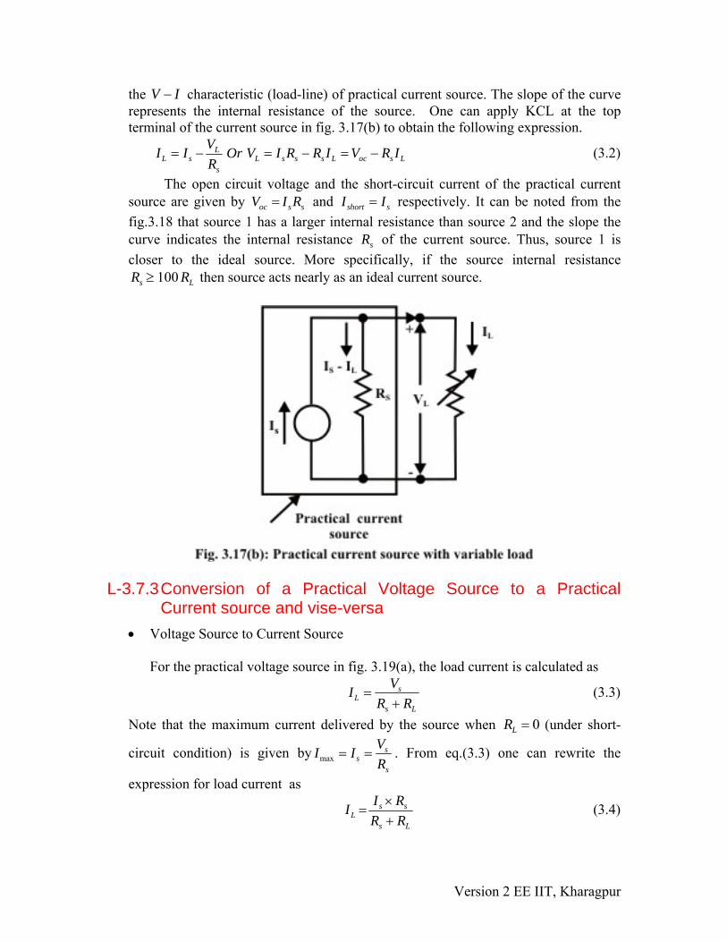
• Another two-terminal element of common use in circuit modeling is `current source` as depicted in fig.3.17. An ideal current source, which is represented by a model in fig. 3.17(a), is a device that delivers a constant current to any load resistance connected across it, no matter what the terminal voltage is developed across the load (i.e., independent of the voltage across its terminals across the terminals).
Version 2 EE IIT, Kharagpur
It can be noted from model of the current source that the current flowing from the source to the load is always constant for any load resistance (see fig. 3.19(a)) i.e. whether is small ( is small) or is large ( is large). The vertical dashed line in fig. 3.18 represents the V
LR LV LR LVI− characteristic of ideal current source. In practice,
when a load is connected across a practical current source, one can observe that the current flowing in load resistance is reduced as the voltage across the current source’s terminal is increased, by increasing the load resistance . Since the distribution of source current in two parallel paths entirely depends on the value of external resistance that connected across the source (current source) terminals. This fact can be realized by introducing a parallel resistance
LR
LR
sR in parallel with the practical current source sI , as shown in fig. 3.17(b). The dark lines in fig. 3.18 show
Version 2 EE IIT, Kharagpur
the V characteristic (load-line) of practical current source. The slope of the curve represents the internal resistance of the source. One can apply KCL at the top terminal of the current source in fig. 3.17(b) to obtain the following expression.
I−
LL s L s s s L oc s
s
VLI I Or V I R R I V R
R= − = − = − I (3.2)
The open circuit voltage and the short-circuit current of the practical current source are given by and oc s sV I R= short sI I= respectively. It can be noted from the fig.3.18 that source 1 has a larger internal resistance than source 2 and the slope the curve indicates the internal resistance sR of the current source. Thus, source 1 is closer to the ideal source. More specifically, if the source internal resistance
100s LR R≥ then source acts nearly as an ideal current source.
L-3.7.3 Conversion of a Practical Voltage Source to a Practical
Current source and vise-versa • Voltage Source to Current Source
For the practical voltage source in fig. 3.19(a), the load current is calculated as
sL
s L
VIR R
=+
(3.3)
Note that the maximum current delivered by the source when (under short-
circuit condition) is given by
0LR =
maxs
ss
VI IR
= = . From eq.(3.3) one can rewrite the
expression for load current as
s sL
s L
I RIR R×
=+
(3.4)
Version 2 EE IIT, Kharagpur
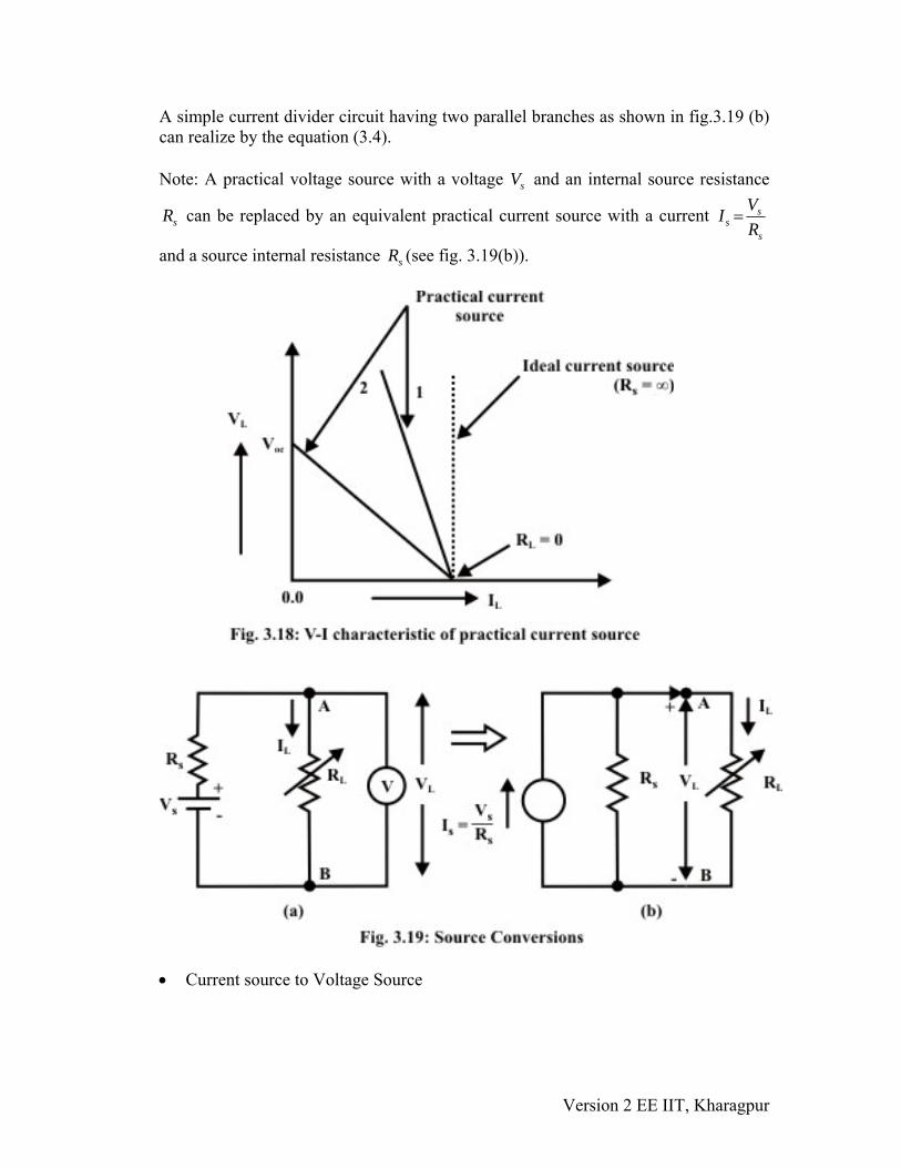
A simple current divider circuit having two parallel branches as shown in fig.3.19 (b) can realize by the equation (3.4). Note: A practical voltage source with a voltage sV and an internal source resistance
sR can be replaced by an equivalent practical current source with a current ss
s
VIR
=
and a source internal resistance sR (see fig. 3.19(b)).
• Current source to Voltage Source
Version 2 EE IIT, Kharagpur
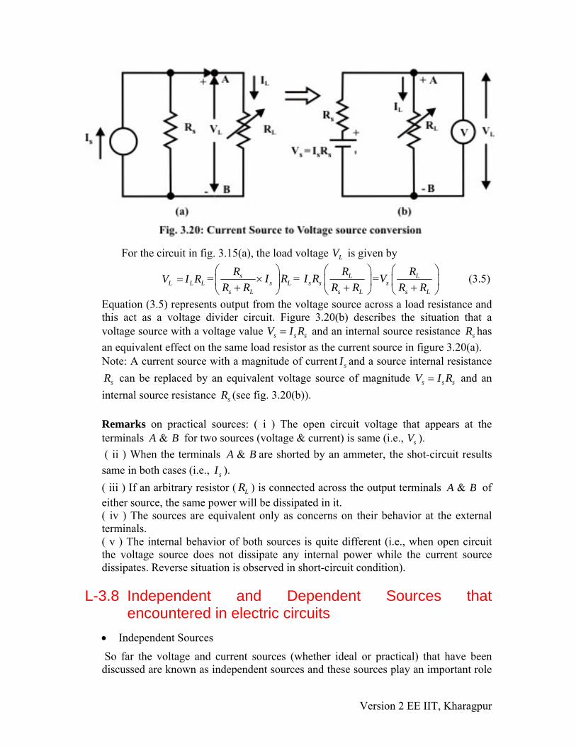
For the circuit in fig. 3.15(a), the load voltage is given by LV
L L LV I R= = ss L
s L
R I RR R
⎛ ⎞×⎜ ⎟+⎝ ⎠
= Ls s
s L
RI RR R
⎛ ⎞⎜ ⎟+⎝ ⎠
= Ls
s L
RVR R
⎛ ⎞⎜ +⎝ ⎠
⎟ (3.5)
Equation (3.5) represents output from the voltage source across a load resistance and this act as a voltage divider circuit. Figure 3.20(b) describes the situation that a voltage source with a voltage value s s sV I R= and an internal source resistance sR has an equivalent effect on the same load resistor as the current source in figure 3.20(a). Note: A current source with a magnitude of current sI and a source internal resistance
sR can be replaced by an equivalent voltage source of magnitude s s sV I R= and an internal source resistance sR (see fig. 3.20(b)). Remarks on practical sources: ( i ) The open circuit voltage that appears at the terminals &A B for two sources (voltage & current) is same (i.e., sV ). ( ii ) When the terminals &A B are shorted by an ammeter, the shot-circuit results same in both cases (i.e., sI ). ( iii ) If an arbitrary resistor ( ) is connected across the output terminals LR &A B of either source, the same power will be dissipated in it. ( iv ) The sources are equivalent only as concerns on their behavior at the external terminals. ( v ) The internal behavior of both sources is quite different (i.e., when open circuit the voltage source does not dissipate any internal power while the current source dissipates. Reverse situation is observed in short-circuit condition).
L-3.8 Independent and Dependent Sources that encountered in electric circuits
• Independent Sources
So far the voltage and current sources (whether ideal or practical) that have been discussed are known as independent sources and these sources play an important role
Version 2 EE IIT, Kharagpur
to drive the circuit in order to perform a specific job. The internal values of these sources (either voltage source or current source) – that is, the generated voltage sV or the generated current sI (see figs. 3.15 & 3.17) are not affected by the load connected across the source terminals or across any other element that exists elsewhere in the circuit or external to the source.
• Dependent Sources
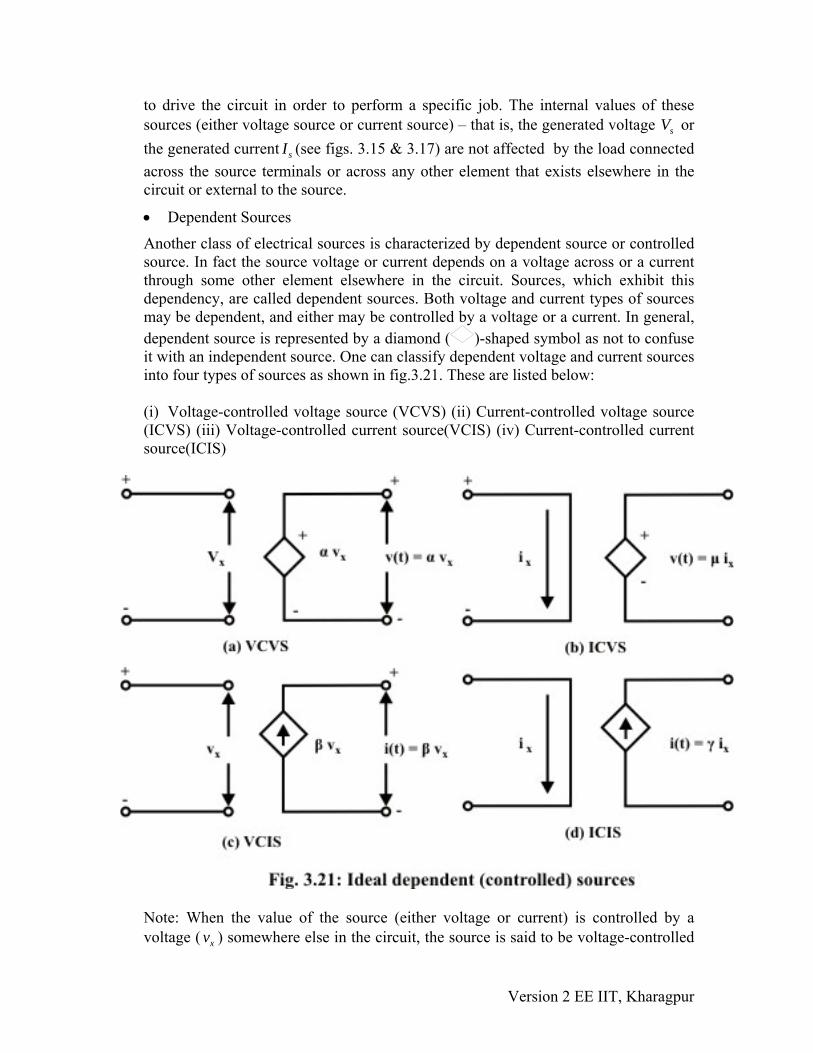
Another class of electrical sources is characterized by dependent source or controlled source. In fact the source voltage or current depends on a voltage across or a current through some other element elsewhere in the circuit. Sources, which exhibit this dependency, are called dependent sources. Both voltage and current types of sources may be dependent, and either may be controlled by a voltage or a current. In general, dependent source is represented by a diamond ( )-shaped symbol as not to confuse it with an independent source. One can classify dependent voltage and current sources into four types of sources as shown in fig.3.21. These are listed below: (i) Voltage-controlled voltage source (VCVS) (ii) Current-controlled voltage source (ICVS) (iii) Voltage-controlled current source(VCIS) (iv) Current-controlled current source(ICIS)
Note: When the value of the source (either voltage or current) is controlled by a voltage ( xv ) somewhere else in the circuit, the source is said to be voltage-controlled
Version 2 EE IIT, Kharagpur
source. On the other hand, when the value of the source (either voltage or current) is controlled by a current ( xi ) somewhere else in the circuit, the source is said to be current-controlled source. KVL and KCL laws can be applied to networks containing such dependent sources. Source conversions, from dependent voltage source models to dependent current source models, or visa-versa, can be employed as needed to simplify the network. One may come across with the dependent sources in many equivalent-circuit models of electronic devices (transistor, BJT(bipolar junction transistor), FET( field-effect transistor) etc.) and transducers.
L-3.9 Understanding Delivering and Absorbing Power by the
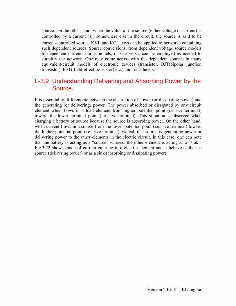
Source. It is essential to differentiate between the absorption of power (or dissipating power) and the generating (or delivering) power. The power absorbed or dissipated by any circuit element when flows in a load element from higher potential point (i.e +ve terminal) toward the lower terminal point (i.e., -ve terminal). This situation is observed when charging a battery or source because the source is absorbing power. On the other hand, when current flows in a source from the lower potential point (i.e., -ve terminal) toward the higher potential point (i.e., +ve terminal), we call that source is generating power or delivering power to the other elements in the electric circuit. In this case, one can note that the battery is acting as a “source” whereas the other element is acting as a “sink”. Fig.3.22 shows mode of current entering in a electric element and it behaves either as source (delivering power) or as a sink (absorbing or dissipating power).
Version 2 EE IIT, Kharagpur
____________________________________________________________________ L.3.10 Test Your Understanding [marks distribution shown
inside the bracket] T.1 If a 30 V source can force 1.5 A through a certain linear circuit, how much current can 10 V force through the same circuit? (Ans. 500 ) [1] .m A
T.2 Find the source voltage sV in the circuit given below [1]
Version 2 EE IIT, Kharagpur
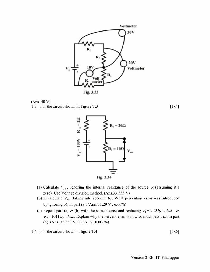
(Ans. 40 V) T.3 For the circuit shown in Figure T.3 [1x4]
(a) Calculate , ignoring the internal resistance of the source outV sR (assuming it’s zero). Use Voltage division method. (Ans.33.333 V)
(b) Recalculate , taking into account outV sR . What percentage error was introduced by ignoring sR in part (a). (Ans. 31.29 V , 6.66%)
(c) Repeat part (a) & (b) with the same source and replacing 1 20 20R by k= Ω Ω & . Explain why the percent error is now so much less than in part
(b). (Ans. 33.333 V, 33.331 V, 0.006%) 2 10 1R by= Ω Ωk
T.4 For the circuit shown in figure T.4 [1x6]
Version 2 EE IIT, Kharagpur
(a) Find , in any order, 2 3, ,I I and I (b) Find, in any order, 1 3, , .eqR R and R (Ans. (a) 20 mA, 30 mA and 100 mA (b) 2 kΩ , 3.33 kΩ and 1kΩ .)
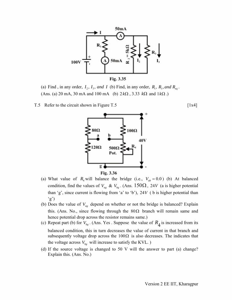
T.5 Refer to the circuit shown in Figure T.5 [1x4]
(a) What value of will balance the bridge (i.e., 4R 0.0abV = ) (b) At balanced
condition, find the values of & . (Ans. 150agV bgV Ω , (a is higher potential than ‘g’, since current is flowing from ‘a’ to ‘b’), ( b is higher potential than ‘g’)
24V24V
(b) Does the value of depend on whether or not the bridge is balanced? Explain this. (Ans. No., since flowing through the 80
agVΩ branch will remain same and
hence potential drop across the resistor remains same.) (c) Repeat part (b) for . (Ans. Yes . Suppose the value of is increased from its
balanced condition, this in turn decreases the value of current in that branch and subsequently voltage drop across the 10
bgV 4R
0Ω is also decreases. The indicates that the voltage across will increase to satisfy the KVL. ) bgV
(d) If the source voltage is changed to 50 V will the answer to part (a) change? Explain this. (Ans. No.)
Version 2 EE IIT, Kharagpur
T.6 If an ideal voltage source and an ideal current source are connected in parallel, then the combination has exactly the same properties as a voltage source alone. Justify this statement. [1]
T.7 If an ideal voltage source and an ideal current source are connected in series, the combination has exactly the same properties as a current source alone. Justify this statement. [1]
T.8 When ideal arbitrary voltage sources are connected in parallel, this connection violates KVL. Justify. [1]
T.9 When ideal arbitrary current sources are connected in series, this connection violates KCL. Justify. [1]
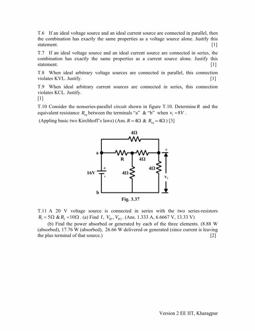
T.10 Consider the nonseries-parallel circuit shown in figure T.10. Determine R and the equivalent resistance eqR between the terminals “a” & “b” when 1 8v V= . (Appling basic two Kirchhoff’s laws) (Ans. 4 & 4eqR R= Ω = Ω ) [3]
T.11 A 20 V voltage source is connected in series with the two series-resistors
. (a) Find 1 25 & 10R R= Ω = Ω 1, ,R R2I V V . (Ans. 1.333 A, 6.6667 V, 13.33 V) (b) Find the power absorbed or generated by each of the three elements. (8.88 W (absorbed), 17.76 W (absorbed), 26.66 W delivered or generated (since current is leaving the plus terminal of that source.) [2]
Version 2 EE IIT, Kharagpur
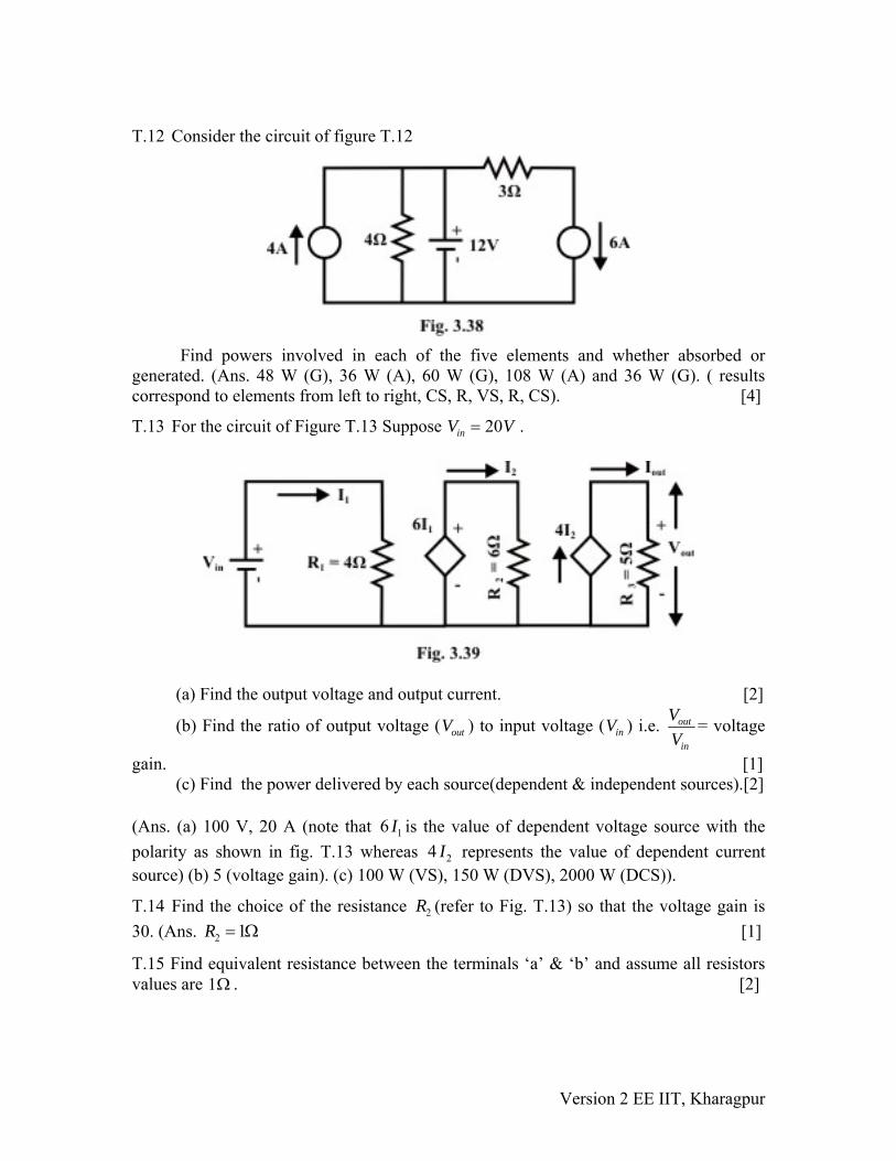
T.12 Consider the circuit of figure T.12
Find powers involved in each of the five elements and whether absorbed or generated. (Ans. 48 W (G), 36 W (A), 60 W (G), 108 W (A) and 36 W (G). ( results correspond to elements from left to right, CS, R, VS, R, CS). [4]
T.13 For the circuit of Figure T.13 Suppose 20inV V= .
(a) Find the output voltage and output current. [2]
(b) Find the ratio of output voltage ( ) to input voltage ( ) i.e. outV inV out
in
VV
= voltage
gain. [1] (c) Find the power delivered by each source(dependent & independent sources).[2] (Ans. (a) 100 V, 20 A (note that 16 I is the value of dependent voltage source with the polarity as shown in fig. T.13 whereas 24 I represents the value of dependent current source) (b) 5 (voltage gain). (c) 100 W (VS), 150 W (DVS), 2000 W (DCS)).
T.14 Find the choice of the resistance (refer to Fig. T.13) so that the voltage gain is 30. (Ans. [1]
2R
2 1R = Ω
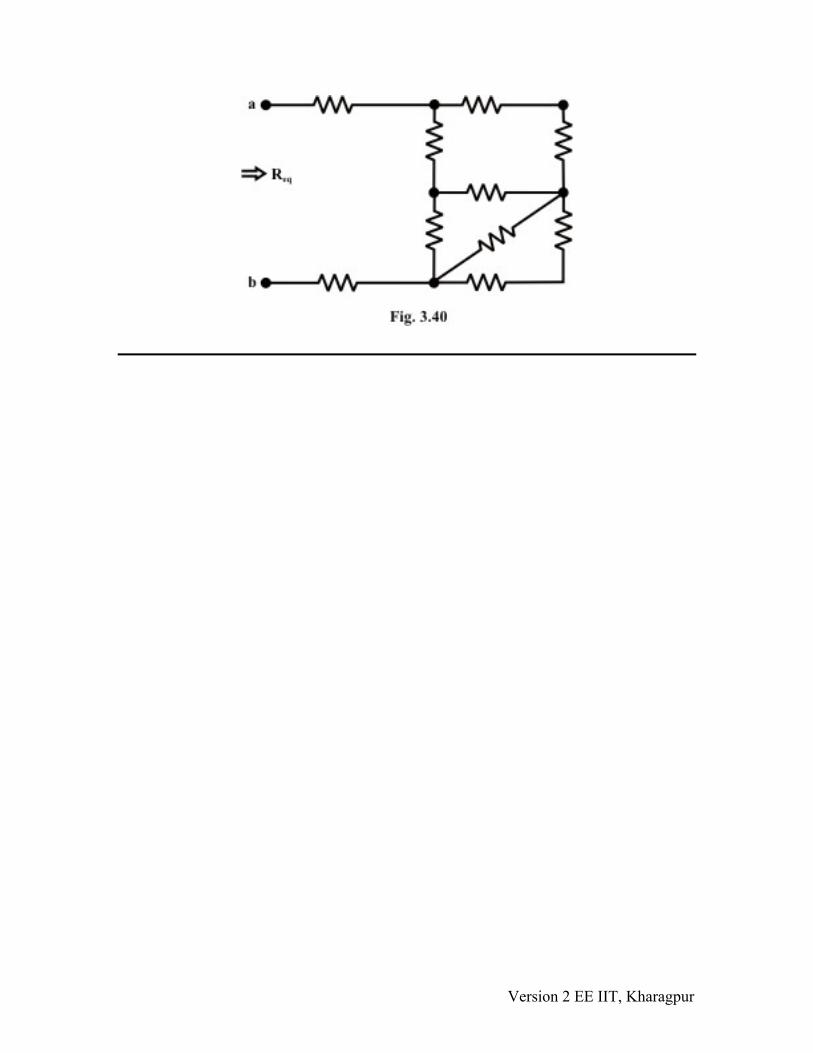
T.15 Find equivalent resistance between the terminals ‘a’ & ‘b’ and assume all resistors values are 1 . [2] Ω
Version 2 EE IIT, Kharagpur
Version 2 EE IIT, Kharagpur