Embed Size (px)
Citation preview
G.PULLA REDDY ENGINEERING COLLEGE (AUTONOMOUS): KURNOOL ELECTRICAL & ELECTRONICS ENGINEERING DEPARTMENT
B.Tech- IV SEMESTER
ELECTRICAL CIRCUITS LABORATORY- (EC (P))
------------------------------------------------------------------------------------------------------------
Prepared by Approved by Page 1 of 6
Dr.G.Kishor Dr. T.Bramhananda Reddy Revision No.0
HEAD, EEE Dept.
TITLE: VERIFICATION OF KCL
& KVL
GPREC/EEE/EXPT.No. ECP-01
DATE: 22-11-2018
OBJECTIVE: To verify Kirchhoff’s voltage law and Kirchhoff’s current law by
(a) Experiment (b) Simulation in PSpice software.
APPARATUS:
Sl.No. Unit Range Type No.
1 Regulated power supply (0-30)V/(0-2)A 1
2 Digital Multimeter 1
3 Ammeter (0-2)A MC 4
4 Rheostats 4
5 Connecting Wires Reqd.
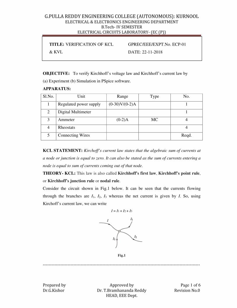
KCL STATEMENT: Kirchoff’s current law states that the algebraic sum of currents at
a node or junction is equal to zero. It can also be stated as the sum of currents entering a
node is equal to sum of currents coming out of that node.
THEORY- KCL: This law is also called Kirchhoff's first law, Kirchhoff's point rule,
or Kirchhoff's junction rule or nodal rule.
Consider the circuit shown in Fig.1 below. It can be seen that the currents flowing
through the branches are I1, I2, I3 whereas the net current is given by I. So, using
Kirchoff’s current law, we can write
I = I1 + I2 + I3
Fig.1
G.PULLA REDDY ENGINEERING COLLEGE (AUTONOMOUS): KURNOOL ELECTRICAL & ELECTRONICS ENGINEERING DEPARTMENT
B.Tech- IV SEMESTER
ELECTRICAL CIRCUITS LABORATORY- (EC (P))
------------------------------------------------------------------------------------------------------------
Prepared by Approved by Page 2 of 6
Dr.G.Kishor Dr. T.Bramhananda Reddy Revision No.0
HEAD, EEE Dept.
TITLE: VERIFICATION OF KCL
& KVL
GPREC/EEE/EXPT.No. ECP-01
DATE: 22-11-2018
APPLICATIONS:
1. Matrix version of Kirchhoff's current law is the basis of most circuit simulation
software, such as PSPICE.
2. Kirchhoff's current law combined with Ohm's Law is used in nodal analysis.
3. KCL is applicable to any lumped network irrespective of the nature of the network;
whether unilateral or bilateral, active or passive, linear or non-linear.
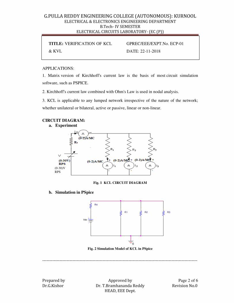
CIRCUIT DIAGRAM:
a. Experiment
Fig. 1 KCL CIRCUIT DIAGRAM
b. Simulation in PSpice
R1
0
R2 R3
Vdc
R4
Fig. 2 Simulation Model of KCL in PSpice
(0-30)V
RPS
G.PULLA REDDY ENGINEERING COLLEGE (AUTONOMOUS): KURNOOL ELECTRICAL & ELECTRONICS ENGINEERING DEPARTMENT
B.Tech- IV SEMESTER
ELECTRICAL CIRCUITS LABORATORY- (EC (P))
------------------------------------------------------------------------------------------------------------
Prepared by Approved by Page 3 of 6
Dr.G.Kishor Dr. T.Bramhananda Reddy Revision No.0
HEAD, EEE Dept.
TITLE: VERIFICATION OF KCL
& KVL
GPREC/EEE/EXPT.No. ECP-01
DATE: 22-11-2018
PROCEDURE FOR KCL:
1. Connections are made as per the circuit diagram shown in Fig.2 & Fig.3
2. By varying the input voltage note down all meter readings.
3. Verify KCL.
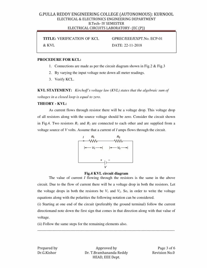
KVL STATEMENT: Kirchoff’s voltage law (KVL) states that the algebraic sum of
voltages in a closed loop is equal to zero.
THEORY - KVL:
As current flows through resistor there will be a voltage drop. This voltage drop
of all resistors along with the source voltage should be zero. Consider the circuit shown
in Fig.4. Two resistors R1 and R2 are connected to each other and are supplied from a
voltage source of V volts. Assume that a current of I amps flows through the circuit.
Fig.4 KVL circuit diagram
The value of current I flowing through the resistors is the same in the above
circuit. Due to the flow of current there will be a voltage drop in both the resistors. Let
the voltage drops in both the resistors be V1 and V2. So, in order to write the voltage
equations along with the polarities the following notation can be considered.
(i) Starting at one end of the circuit (preferably the ground terminal) follow the current
directionand note down the first sign that comes in that direction along with that value of
voltage.
(ii) Follow the same steps for the remaining elements also.

G.PULLA REDDY ENGINEERING COLLEGE (AUTONOMOUS): KURNOOL ELECTRICAL & ELECTRONICS ENGINEERING DEPARTMENT
B.Tech- IV SEMESTER
ELECTRICAL CIRCUITS LABORATORY- (EC (P))
------------------------------------------------------------------------------------------------------------
Prepared by Approved by Page 4 of 6
Dr.G.Kishor Dr. T.Bramhananda Reddy Revision No.0
HEAD, EEE Dept.
TITLE: VERIFICATION OF KCL
& KVL
GPREC/EEE/EXPT.No. ECP-01
DATE: 22-11-2018
Using the above methodology, the voltage equations may be written as
–V + V1 + V2 = 0 But V1 = IR1 and V2 = IR2, which implies
–V + IR1 + IR2 = 0
Or IR1 + IR2 = V
Or
21 RR
VI
+=
APPLICATIONS OF KVL:
1. KVL is used to determine the values of unknown currents and their direction.
2. Useful to find the unknown values in complex circuits and networks (not suitable
for high frequency circuit).
3. Kirchhoff’s Laws are useful in understanding the transfer of energy through an
electric circuit.
a. Experiment
Fig. 3 KVL CIRCUIT DIAGRAM
(0-30)V
RPS
G.PULLA REDDY ENGINEERING COLLEGE (AUTONOMOUS): KURNOOL ELECTRICAL & ELECTRONICS ENGINEERING DEPARTMENT
B.Tech- IV SEMESTER
ELECTRICAL CIRCUITS LABORATORY- (EC (P))
------------------------------------------------------------------------------------------------------------
Prepared by Approved by Page 5 of 6
Dr.G.Kishor Dr. T.Bramhananda Reddy Revision No.0
HEAD, EEE Dept.
TITLE: VERIFICATION OF KCL
& KVL
GPREC/EEE/EXPT.No. ECP-01
DATE: 22-11-2018
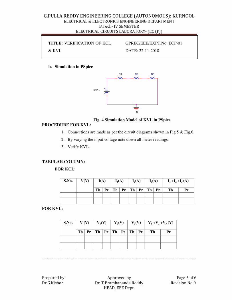
b. Simulation in PSpice
30Vdc
R2R1
0
R3
Fig. 4 Simulation Model of KVL in PSpice
PROCEDURE FOR KVL:
1. Connections are made as per the circuit diagrams shown in Fig.5 & Fig.6.
2. By varying the input voltage note down all meter readings.
3. Verify KVL.
TABULAR COLUMN:
FOR KCL:
FOR KVL:
S.No. V(V) I(A) I1(A) I2(A) I3(A) I1 +I2 +I3 (A)
Th Pr Th Pr Th Pr Th Pr Th Pr
S.No. V (V) V1(V) V2(V) V3(V) V1 +V2 +V3 (V)
Th Pr Th Pr Th Pr Th Pr Th Pr

G.PULLA REDDY ENGINEERING COLLEGE (AUTONOMOUS): KURNOOL ELECTRICAL & ELECTRONICS ENGINEERING DEPARTMENT
B.Tech- IV SEMESTER
ELECTRICAL CIRCUITS LABORATORY- (EC (P))
------------------------------------------------------------------------------------------------------------
Prepared by Approved by Page 6 of 6
Dr.G.Kishor Dr. T.Bramhananda Reddy Revision No.0
HEAD, EEE Dept.
TITLE: VERIFICATION OF KCL
& KVL
GPREC/EEE/EXPT.No. ECP-01
DATE: 22-11-2018
RESULT: Kirchhoff’s laws are verified.
Questions on KCL & KVL:
1. Define KVL
2. Define KCL
3. Define Ohm’s law
4. What are the applications of KVL and KCL?
5. In nodal analysis which law will be used?
6. In mesh analysis which law will be used?

G.PULLA REDDY ENGINEERING COLLEGE (AUTONOMOUS): KURNOOL ELECTRICAL & ELECTRONICS ENGINEERING DEPARTMENT
B.Tech- IV Semester
ELECTRICAL CIRCUITS LABORATORY- (EC (P))
-----------------------------------------------------------------------------------------------------------
Prepared by Approved by Page 1 of 7
Dr.G.Kishor Dr. T.Bramhananda Reddy Revision No.0
HEAD, EEE Dept.
TITLE: VERIFICATION OF
MAXIMUM POWER TRANSFER
THEOREM
GPREC/EEE/EXPT.No. ECP-02
DATE: 22-11-2018
OBJECTIVE: To verify Maximum Power Transfer theorem by (a) Simulation in PSpice
software (b) Experiment.
APPARATUS:
Sl.No. Unit Range Type No. Required
1 Voltmeter (0-100V) MC 1
2 Ammeter (0-5)A MC 1
3 Rheostat - 2
4 Connecting Wires Reqd.
STATEMENT: Maximum power transfer theorem states that the power delivered by an
active network to a load connected across its terminals is maximum, when the impedance
of the load is the complex conjugate of the active network impedance.
THEORY:
In this theorem we shall consider different cases
Case (i): When the load is purely resistive
Consider a network delivering power to the load as shown in figure given below
Fig. 1
Current delivered to the load is gLg
g
jXRR
Ei
++=
)(
G.PULLA REDDY ENGINEERING COLLEGE (AUTONOMOUS): KURNOOL ELECTRICAL & ELECTRONICS ENGINEERING DEPARTMENT
B.Tech- IV Semester
ELECTRICAL CIRCUITS LABORATORY- (EC (P))
-----------------------------------------------------------------------------------------------------------
Prepared by Approved by Page 2 of 7
Dr.G.Kishor Dr. T.Bramhananda Reddy Revision No.0
HEAD, EEE Dept.
TITLE: VERIFICATION OF
MAXIMUM POWER TRANSFER
THEOREM
GPREC/EEE/EXPT.No. ECP-02
DATE: 22-11-2018
Power delivered to the load is LRi2
22
2
)( gLg
Lg
XRR
REP
++
= watts
The condition when the power delivered to the load is maximum, can be formed if
0=
LdR
dP
0)( 22
2
=
++ gLg
Lg
L XRR
RE
dR
d
Simplifying we get 222ggL XRR += or 22
ggL XRR +=
Therefore load resistance gL ZR =
If 0=gX then gL RR =
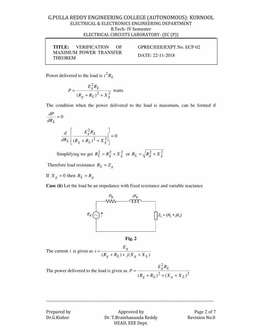
Case (ii) Let the load be an impedance with fixed resistance and variable reactance
Fig. 2
The current i is given as )()( LgLg
g
XXjRR
Ei
+++=
The power delivered to the load is given as 22
2
)()( LgLg
Lg
XXRR
REP
+++
=

G.PULLA REDDY ENGINEERING COLLEGE (AUTONOMOUS): KURNOOL ELECTRICAL & ELECTRONICS ENGINEERING DEPARTMENT
B.Tech- IV Semester
ELECTRICAL CIRCUITS LABORATORY- (EC (P))
-----------------------------------------------------------------------------------------------------------
Prepared by Approved by Page 3 of 7
Dr.G.Kishor Dr. T.Bramhananda Reddy Revision No.0
HEAD, EEE Dept.
TITLE: VERIFICATION OF
MAXIMUM POWER TRANSFER
THEOREM
GPREC/EEE/EXPT.No. ECP-02
DATE: 22-11-2018
The condition can be found by using 0=
LdX
dP
i.e. 0)()(22
2
=
+++ LgLg
Lg
L XXRR
RE
dX
d
Solving this we get
gL XX −=
The reactance of the load is of the same magnitude as the reactance of the network but is
of opposite sign.
Case (iii) Let the load be an impedance with fixed reactance and variable resistance
The power 22
2
)()( LgLg
Lg
XXRR
REP
+++
=
The condition can be found by 0=
LdR
dP
0)()(22
2
=
+++ LgLg
Lg
L XXRR
RE
dR
d
Solving this we get
LgLLggL jXZRorjXjXRR +=++= )(
General case: If the load is an impedance with variable reactance and resistance, then the
maximum power would be delivered when gL ZZ = i.e gLgL XXandRR −==
Procedure to verify Maximum Power Transfer Theorem
i. In order to verify maximum power transfer theorem the network is reduced in
such a way that the network consists of a single source, active network impedance
and the load impedance.
G.PULLA REDDY ENGINEERING COLLEGE (AUTONOMOUS): KURNOOL ELECTRICAL & ELECTRONICS ENGINEERING DEPARTMENT
B.Tech- IV Semester
ELECTRICAL CIRCUITS LABORATORY- (EC (P))
-----------------------------------------------------------------------------------------------------------
Prepared by Approved by Page 4 of 7
Dr.G.Kishor Dr. T.Bramhananda Reddy Revision No.0
HEAD, EEE Dept.
TITLE: VERIFICATION OF
MAXIMUM POWER TRANSFER
THEOREM
GPREC/EEE/EXPT.No. ECP-02
DATE: 22-11-2018
ii. The condition for maximum power transfer is then verified by checking at the
condition when the impedance of the load is the complex conjugate of the active
network impedance.
Application:
1. In communication system, maximum power transfer is always sought. For
example in public address system, the circuit is adjusted for maximum power
transfer by making load resistance (speaker) equal to the source resistance
(amplifier). When source and load have the same resistance, they are said to be
matched.
2. In car engines, the power delivered to the starter motor of the car will depend
upon the effective resistance of the motor and the internal resistance of the
battery. If the two resistances are equal, maximum power will be transferred to
the motor to turn to the engine.
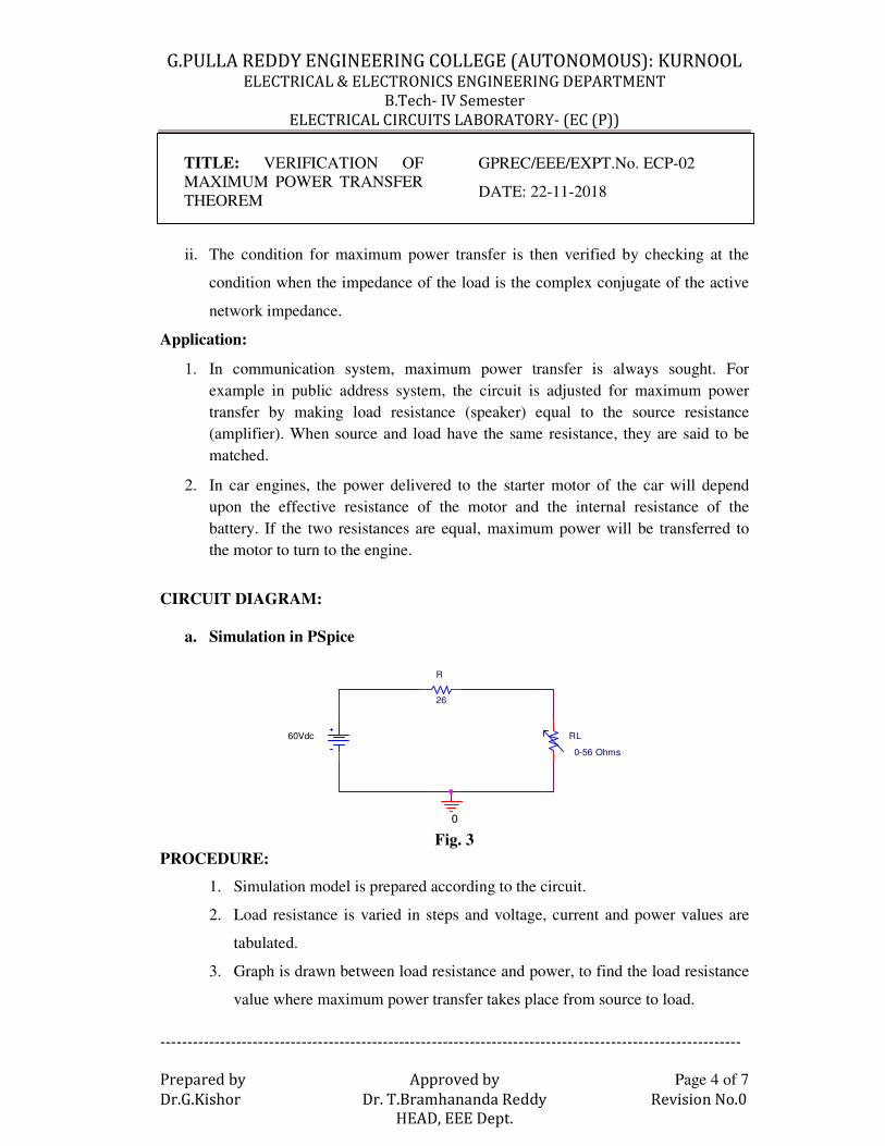
CIRCUIT DIAGRAM:
a. Simulation in PSpice
0
60Vdc
R
26
RL
0-56 Ohms
Fig. 3
PROCEDURE:
1. Simulation model is prepared according to the circuit.
2. Load resistance is varied in steps and voltage, current and power values are
tabulated.
3. Graph is drawn between load resistance and power, to find the load resistance
value where maximum power transfer takes place from source to load.
G.PULLA REDDY ENGINEERING COLLEGE (AUTONOMOUS): KURNOOL ELECTRICAL & ELECTRONICS ENGINEERING DEPARTMENT
B.Tech- IV Semester
ELECTRICAL CIRCUITS LABORATORY- (EC (P))
-----------------------------------------------------------------------------------------------------------
Prepared by Approved by Page 5 of 7
Dr.G.Kishor Dr. T.Bramhananda Reddy Revision No.0
HEAD, EEE Dept.
TITLE: VERIFICATION OF
MAXIMUM POWER TRANSFER
THEOREM
GPREC/EEE/EXPT.No. ECP-02
DATE: 22-11-2018
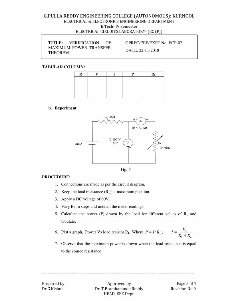
TABULAR COLUMN:
R V I P RL
b. Experiment
Fig. 4
PROCEDURE:
1. Connections are made as per the circuit diagram.
2. Keep the load resistance (RL) at maximum position.
3. Apply a DC voltage of 60V.
4. Vary RL in steps and note all the meter readings.
5. Calculate the power (P) drawn by the load for different values of RL and
tabulate.
6. Plot a graph, Power Vs load resistor RL. Where LRIP2
= ; LS
S
RR
VI
+=
7. Observe that the maximum power is drawn when the load resistance is equal
to the source resistance.
(0-100)V
MC
(0-5)A / MC
(0-56)Ω
26Ω
G.PULLA REDDY ENGINEERING COLLEGE (AUTONOMOUS): KURNOOL ELECTRICAL & ELECTRONICS ENGINEERING DEPARTMENT
B.Tech- IV Semester
ELECTRICAL CIRCUITS LABORATORY- (EC (P))
-----------------------------------------------------------------------------------------------------------
Prepared by Approved by Page 6 of 7
Dr.G.Kishor Dr. T.Bramhananda Reddy Revision No.0
HEAD, EEE Dept.
TITLE: VERIFICATION OF
MAXIMUM POWER TRANSFER
THEOREM
GPREC/EEE/EXPT.No. ECP-02
DATE: 22-11-2018
TABULAR COLUMN:
S.No. V I P RL
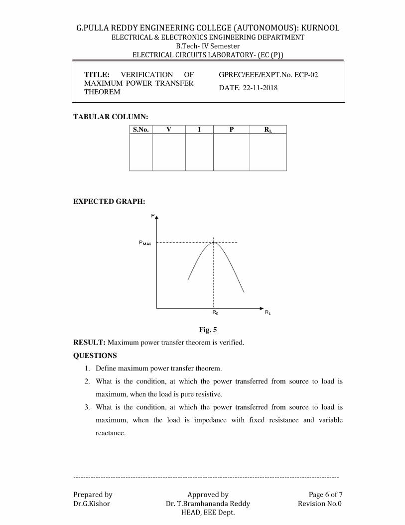
EXPECTED GRAPH:
Fig. 5
RESULT: Maximum power transfer theorem is verified.
QUESTIONS
1. Define maximum power transfer theorem.
2. What is the condition, at which the power transferred from source to load is
maximum, when the load is pure resistive.
3. What is the condition, at which the power transferred from source to load is
maximum, when the load is impedance with fixed resistance and variable
reactance.
G.PULLA REDDY ENGINEERING COLLEGE (AUTONOMOUS): KURNOOL ELECTRICAL & ELECTRONICS ENGINEERING DEPARTMENT
B.Tech- IV Semester
ELECTRICAL CIRCUITS LABORATORY- (EC (P))
-----------------------------------------------------------------------------------------------------------
Prepared by Approved by Page 7 of 7
Dr.G.Kishor Dr. T.Bramhananda Reddy Revision No.0
HEAD, EEE Dept.
TITLE: VERIFICATION OF
MAXIMUM POWER TRANSFER
THEOREM
GPREC/EEE/EXPT.No. ECP-02
DATE: 22-11-2018
4. What is the condition, at which the power transferred from source to load is
maximum, when the load is impedance with fixed reactance and variable
resistance.
5. What is the condition, at which the power transferred from source to load is
maximum, when the load is impedance with resistance and reactance are variable.
6. What are the applications of Maximum power transfer theorem?
G.PULLA REDDY ENGINEERING COLLEGE (AUTONOMOUS): KURNOOL ELECTRICAL & ELECTRONICS ENGINEERING DEPARTMENT
B.Tech- IV SEMESTER
ELECTRICAL CIRCUITS LABORATORY –EC(P)
------------------------------------------------------------------------------------------------------------
Prepared by Approved by Page 1 of 5
Dr.G.Kishor Dr. T.Bramhananda Reddy Revision No.0
HEAD, EEE Dept.
TITLE: VERIFICATION OF
RECIPROCITY THEOREM
GPREC/EEE/EXPT.No. ECP-03
DATE: 22-11-2018
OBJECTIVE: To Verify Reciprocity theorem by (a) Experiment (b) Simulation in
PSpice software.
APPARATUS:
Sl.No. Unit Range Type No.
1 Regulated Power Supply (0-30)V/(0-2)A 1
2 Ammeter (0-2)A MC 1
3 Rheostat 3
4 Digital Multimeter 1
Connecting Wires Reqd.
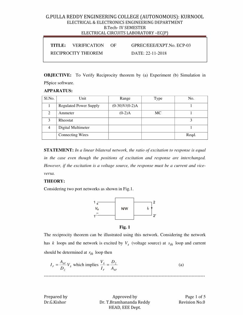
STATEMENT: In a linear bilateral network, the ratio of excitation to response is equal
in the case even though the positions of excitation and response are interchanged.
However, if the excitation is a voltage source, the response must be a current and vice-
versa.
THEORY:
Considering two port networks as shown in Fig.1.
Fig. 1
The reciprocity theorem can be illustrated using this network. Considering the network
has k loops and the network is excited by sV (voltage source) at ths loop and current
should be determined at thr loop then
sz
srr V
D
AI = which implies
sr
z
r
s
A
D
I
V= (a)

G.PULLA REDDY ENGINEERING COLLEGE (AUTONOMOUS): KURNOOL ELECTRICAL & ELECTRONICS ENGINEERING DEPARTMENT
B.Tech- IV SEMESTER
ELECTRICAL CIRCUITS LABORATORY –EC(P)
------------------------------------------------------------------------------------------------------------
Prepared by Approved by Page 2 of 5
Dr.G.Kishor Dr. T.Bramhananda Reddy Revision No.0
HEAD, EEE Dept.
TITLE: VERIFICATION OF
RECIPROCITY THEOREM
GPREC/EEE/EXPT.No. ECP-03
DATE: 22-11-2018
where srA is a cofactor
zD is the impedance of the network
z
sr
D
A is the admittance
As we interchange the positions of response and excitation, the circuit is
Fig. 2
rz
rss V
D
AI = which implies
rs
z
s
r
A
D
I
V= (b)
From equations a and b
sr
z
r
s
A
D
I
V= and
rs
z
s
r
A
D
I
V=
If srA and rsA are equal we can have a symmetric network with RLC elements and no
controlled sources
s
r
r
s
I
V
I
V=
Hence the theorem can be proved
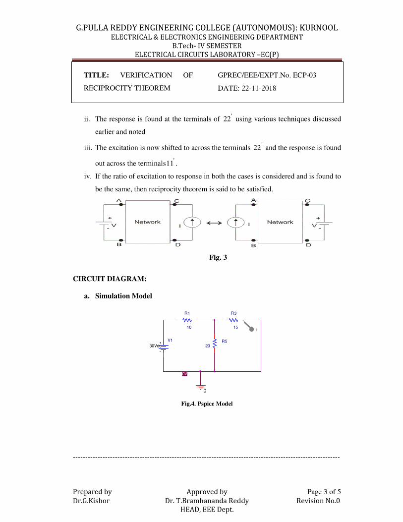
Procedure to verify Reciprocity theorem
i. In order to verify reciprocity theorem consider a network in which excitation is
placed at terminals '11 and response is to be found out at '22 .
G.PULLA REDDY ENGINEERING COLLEGE (AUTONOMOUS): KURNOOL ELECTRICAL & ELECTRONICS ENGINEERING DEPARTMENT
B.Tech- IV SEMESTER
ELECTRICAL CIRCUITS LABORATORY –EC(P)
------------------------------------------------------------------------------------------------------------
Prepared by Approved by Page 3 of 5
Dr.G.Kishor Dr. T.Bramhananda Reddy Revision No.0
HEAD, EEE Dept.
TITLE: VERIFICATION OF
RECIPROCITY THEOREM
GPREC/EEE/EXPT.No. ECP-03
DATE: 22-11-2018
ii. The response is found at the terminals of '22 using various techniques discussed
earlier and noted
iii. The excitation is now shifted to across the terminals '22 and the response is found
out across the terminals '11 .
iv. If the ratio of excitation to response in both the cases is considered and is found to
be the same, then reciprocity theorem is said to be satisfied.
Fig. 3
CIRCUIT DIAGRAM:
a. Simulation Model
0V
I
0
V1
30Vdc
R1
10
R5
20
R3
15
Fig.4. Pspice Model

G.PULLA REDDY ENGINEERING COLLEGE (AUTONOMOUS): KURNOOL ELECTRICAL & ELECTRONICS ENGINEERING DEPARTMENT
B.Tech- IV SEMESTER
ELECTRICAL CIRCUITS LABORATORY –EC(P)
------------------------------------------------------------------------------------------------------------
Prepared by Approved by Page 4 of 5
Dr.G.Kishor Dr. T.Bramhananda Reddy Revision No.0
HEAD, EEE Dept.
TITLE: VERIFICATION OF
RECIPROCITY THEOREM
GPREC/EEE/EXPT.No. ECP-03
DATE: 22-11-2018
0
R3
15
0V
I
R5
20
R1
10
V1
30Vdc
Fig.5. Pspice Model
b. Experiment
Fig.6
Fig.7
(0-30)V
RPS
(0-2)A/MC
(0-2)A/MC
(0-30)V
RPS
G.PULLA REDDY ENGINEERING COLLEGE (AUTONOMOUS): KURNOOL ELECTRICAL & ELECTRONICS ENGINEERING DEPARTMENT
B.Tech- IV SEMESTER
ELECTRICAL CIRCUITS LABORATORY –EC(P)
------------------------------------------------------------------------------------------------------------
Prepared by Approved by Page 5 of 5
Dr.G.Kishor Dr. T.Bramhananda Reddy Revision No.0
HEAD, EEE Dept.
TITLE: VERIFICATION OF
RECIPROCITY THEOREM
GPREC/EEE/EXPT.No. ECP-03
DATE: 22-11-2018
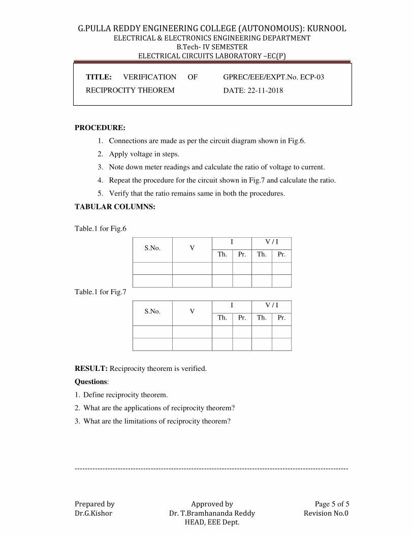
PROCEDURE:
1. Connections are made as per the circuit diagram shown in Fig.6.
2. Apply voltage in steps.
3. Note down meter readings and calculate the ratio of voltage to current.
4. Repeat the procedure for the circuit shown in Fig.7 and calculate the ratio.
5. Verify that the ratio remains same in both the procedures.
TABULAR COLUMNS:
Table.1 for Fig.6
S.No. V I V / I
Th. Pr. Th. Pr.
Table.1 for Fig.7
S.No. V I V / I
Th. Pr. Th. Pr.
RESULT: Reciprocity theorem is verified.
Questions:
1. Define reciprocity theorem.
2. What are the applications of reciprocity theorem?
3. What are the limitations of reciprocity theorem?

G.PULLA REDDY ENGINEERING COLLEGE (AUTONOMOUS): KURNOOL ELECTRICAL & ELECTRONICS ENGINEERING DEPARTMENT
B.Tech- IV SEMESTER
ELECTRICAL CIRCUITS LABORATORY - (EC (P))
------------------------------------------------------------------------------------------------------------
Prepared by Approved by Page 1 of 5
Dr.G.Kishor Dr. T.Bramhananda Reddy Revision No.0
HEAD, EEE Dept.
TITLE: VERIFICATION OF
SUPERPOSITION THEOREM
GPREC/EEE/EXPT.No. ECP-03
DATE: 22-11-2018
OBJECTIVE: To Verify Superposition theorem by (a) Experiment (b) Simulation in
PSpice software.
APPARATUS:
Sl.No. Unit Range Type No.
1 Regulated power supply (0-30)V/(0-2)A 2
2 Ammeter (0-2)A MC 1
3 Rheostat 3
4 Connecting Wires - Reqd.
STATEMENT: In any linear network with several independent sources and dependent
sources, the overall response in any part of the network is equal to the sum of the
individual responses due to each independent source with all other independent sources
reduced to zero.
(or)
“According to superposition theorem, in any linear network containing two or more
sources, the response in any element is equal to the algebraic sum of the responses
caused by the individual sources acting alone while the other sources are non-
operative.”
This means all independent voltages are shorted and all independent current
sources are open circuited. If the sources contain internal impedances, the sources are
replaced by the impedances.
THEORY: Superposition theorem is valid only for linear systems. Superposition
theorem is not applicable to power. This theorem can be applicable to voltages and
currents. The above statement can be proved by the following explanation.
In linear systems, currents are propositional to the voltages VIα
G.PULLA REDDY ENGINEERING COLLEGE (AUTONOMOUS): KURNOOL ELECTRICAL & ELECTRONICS ENGINEERING DEPARTMENT
B.Tech- IV SEMESTER
ELECTRICAL CIRCUITS LABORATORY - (EC (P))
------------------------------------------------------------------------------------------------------------
Prepared by Approved by Page 2 of 5
Dr.G.Kishor Dr. T.Bramhananda Reddy Revision No.0
HEAD, EEE Dept.
TITLE: VERIFICATION OF
SUPERPOSITION THEOREM
GPREC/EEE/EXPT.No. ECP-03
DATE: 22-11-2018
In this theorem, we add individual currents of a branch due to each source taking at a
time to get the resultant current. This is similar to voltages.
∴ We can have .......21 ++= III
.......21 ++= VVV
Procedure to verify Superposition Theorem
i. While evaluating the superposition theorem only one source (voltage source or
current source) is kept in the network while making the other sources equal to
zero. This implies to each source present in the network
ii. If there are 2 voltage sources, 21,VV and one current source I in a network, first
1V is considered to be present in the network while making the other voltage
source and current source equal to zero
iii. The corresponding parameter (current or voltage) is found in the particular
element when 1V is present.
iv. In the next step 2V is considered while making the other sources constant and the
corresponding parameter in the particular element is found out
v. The same procedure is followed when the current source is considered
vi. The values of parameter across the particular element obtained during various
sources is added and verified with the value of parameter obtained when all the
three sources are present in the network
vii. The theorem is said to be satisfied if both the values are equal
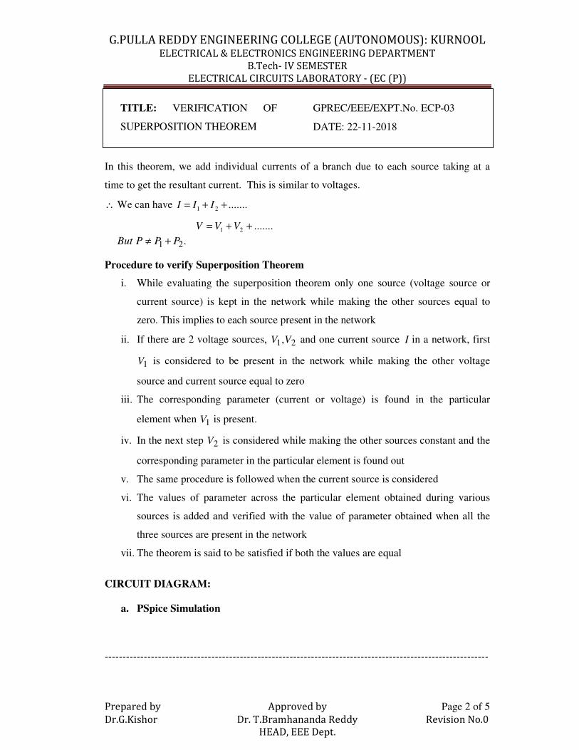
CIRCUIT DIAGRAM:
a. PSpice Simulation
.21 PPPBut +≠

G.PULLA REDDY ENGINEERING COLLEGE (AUTONOMOUS): KURNOOL ELECTRICAL & ELECTRONICS ENGINEERING DEPARTMENT
B.Tech- IV SEMESTER
ELECTRICAL CIRCUITS LABORATORY - (EC (P))
------------------------------------------------------------------------------------------------------------
Prepared by Approved by Page 3 of 5
Dr.G.Kishor Dr. T.Bramhananda Reddy Revision No.0
HEAD, EEE Dept.
TITLE: VERIFICATION OF
SUPERPOSITION THEOREM
GPREC/EEE/EXPT.No. ECP-03
DATE: 22-11-2018
R2R1
V1
0-30 Vdc
0
V2
0-30Vdc
R3
Fig.1
R3V1
0-30 Vdc
R2R1
0
Fig.2
R2R1
R3 V2
0-30Vdc
0
Fig.3
G.PULLA REDDY ENGINEERING COLLEGE (AUTONOMOUS): KURNOOL ELECTRICAL & ELECTRONICS ENGINEERING DEPARTMENT
B.Tech- IV SEMESTER
ELECTRICAL CIRCUITS LABORATORY - (EC (P))
------------------------------------------------------------------------------------------------------------
Prepared by Approved by Page 4 of 5
Dr.G.Kishor Dr. T.Bramhananda Reddy Revision No.0
HEAD, EEE Dept.
TITLE: VERIFICATION OF
SUPERPOSITION THEOREM
GPREC/EEE/EXPT.No. ECP-03
DATE: 22-11-2018
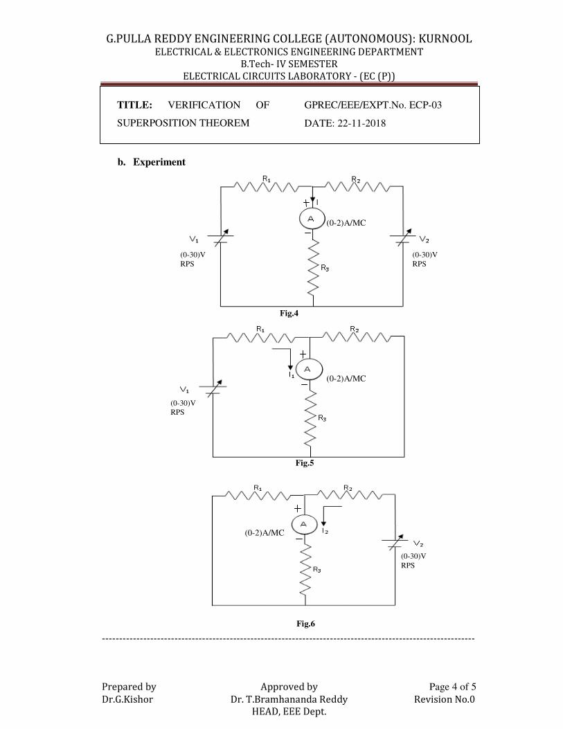
b. Experiment
Fig.4
Fig.5
Fig.6
(0-30)V
RPS
(0-30)V
RPS
(0-30)V
RPS
(0-30)V
RPS
(0-2)A/MC
(0-2)A/MC
(0-2)A/MC
G.PULLA REDDY ENGINEERING COLLEGE (AUTONOMOUS): KURNOOL ELECTRICAL & ELECTRONICS ENGINEERING DEPARTMENT
B.Tech- IV SEMESTER
ELECTRICAL CIRCUITS LABORATORY - (EC (P))
------------------------------------------------------------------------------------------------------------
Prepared by Approved by Page 5 of 5
Dr.G.Kishor Dr. T.Bramhananda Reddy Revision No.0
HEAD, EEE Dept.
TITLE: VERIFICATION OF
SUPERPOSITION THEOREM
GPREC/EEE/EXPT.No. ECP-03
DATE: 22-11-2018
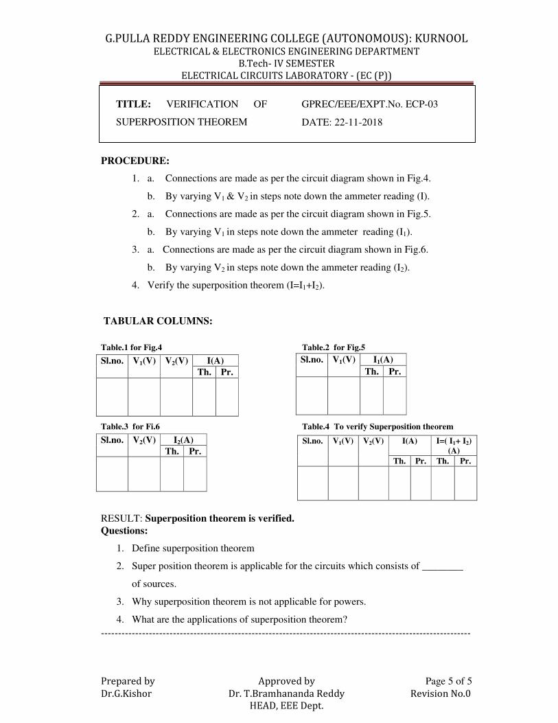
PROCEDURE:
1. a. Connections are made as per the circuit diagram shown in Fig.4.
b. By varying V1 & V2 in steps note down the ammeter reading (I).
2. a. Connections are made as per the circuit diagram shown in Fig.5.
b. By varying V1 in steps note down the ammeter reading (I1).
3. a. Connections are made as per the circuit diagram shown in Fig.6.
b. By varying V2 in steps note down the ammeter reading (I2).
4. Verify the superposition theorem (I=I1+I2).
TABULAR COLUMNS:
Table.1 for Fig.4
Table.2 for Fig.5
Table.3 for Fi.6
Table.4 To verify Superposition theorem
RESULT: Superposition theorem is verified.
Questions:
1. Define superposition theorem
2. Super position theorem is applicable for the circuits which consists of ________
of sources.
3. Why superposition theorem is not applicable for powers.
4. What are the applications of superposition theorem?
Sl.no. V1(V) V2(V) I(A)
Th. Pr.
Sl.no. V1(V) I1(A)
Th. Pr.
Sl.no. V2(V) I2(A)
Th. Pr.
Sl.no. V1(V) V2(V) I(A) I=( I1+ I2)
(A)
Th. Pr. Th. Pr.
G.PULLA REDDY ENGINEERING COLLEGE (AUTONOMOUS): KURNOOL ELECTRICAL & ELECTRONICS ENGINEERING DEPARTMENT
B.Tech- IV SEMESTER
ELECTRICAL CIRCUITS LABORATORY - (EC (P))
-----------------------------------------------------------------------------------------------------------
Prepared by Approved by Page 1 of 5
Dr.G.Kishor Dr. T.Bramhananda Reddy Revision No.0
HEAD, EEE Dept.
TITLE: VERIFICATION OF
THEVENIN’S THEOREM
GPREC/EEE/EXPT.No. ECP-04
DATE: 22-11-2018
OBJECTIVE: To verify Thevenin’s theorem by (a) Simulation in PSpice software
(b) Experiment.
APPARATUS:
Sl.No. Unit Range Type No.
1 Regulated power supply (0-30)V/(0-2)A 1
2 Ammeter (0-2)A MC 1
3 Rheostat 4
4 Digital Multimeter 1
5 Connecting Wires Reqd.
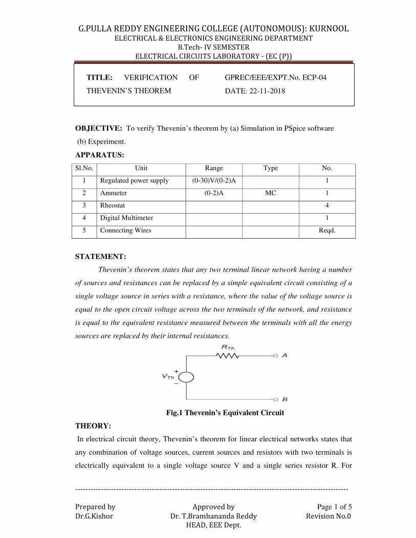
STATEMENT:
Thevenin’s theorem states that any two terminal linear network having a number
of sources and resistances can be replaced by a simple equivalent circuit consisting of a
single voltage source in series with a resistance, where the value of the voltage source is
equal to the open circuit voltage across the two terminals of the network, and resistance
is equal to the equivalent resistance measured between the terminals with all the energy
sources are replaced by their internal resistances.
Fig.1 Thevenin’s Equivalent Circuit
THEORY:
In electrical circuit theory, Thevenin’s theorem for linear electrical networks states that
any combination of voltage sources, current sources and resistors with two terminals is
electrically equivalent to a single voltage source V and a single series resistor R. For

G.PULLA REDDY ENGINEERING COLLEGE (AUTONOMOUS): KURNOOL ELECTRICAL & ELECTRONICS ENGINEERING DEPARTMENT
B.Tech- IV SEMESTER
ELECTRICAL CIRCUITS LABORATORY - (EC (P))
-----------------------------------------------------------------------------------------------------------
Prepared by Approved by Page 2 of 5
Dr.G.Kishor Dr. T.Bramhananda Reddy Revision No.0
HEAD, EEE Dept.
TITLE: VERIFICATION OF
THEVENIN’S THEOREM
GPREC/EEE/EXPT.No. ECP-04
DATE: 22-11-2018
single frequency AC systems, the theorem can also be applied to general impedances, not
just resistors. Any complex network can be reduced to a Thevenin's equivalent circuit
consist of a single voltage source and series resistance connected to a load.
Procedure to obtain Thevenin’s equivalent circuit
i. Temporally remove the load resistance whose current is required.
ii. Find the open circuit voltage VOC which appear across the two terminals from
where the load resistance has been removed. It is also called Thevenin’s voltage
Vth.
iii. Calculate the resistance of the whole network as looked into from these two
terminals, after all voltage sources are replaced by short circuit and current
sources are replaced by open circuit leaving internal resistance (if any). It is also
called Thevenin’s resistance Rth.
iv. Replace the entire network by a single Thevenin’s voltage source whose voltage
is Vth and whose resistance is Rth.
v. Connect the load resistance (RL) back to its terminals from where it was
previously removed.
vi. Finally calculate the current flowing though RL by using equation.
IL = Lth
th
RR
V
+
Applications of Thevenin's Theorem:
• Thevenin's Theorem is especially useful in analyzing power systems and other
circuits where one particular resistor in the circuit (called the “load” resistor) is
subject to change, and re-calculation of the circuit is necessary with each trial
value of load resistance, to determine voltage across it and current through it.
• Source modeling and resistance measurement using the Wheatstone bridge
provide applications for Thevenin’s theorem.
G.PULLA REDDY ENGINEERING COLLEGE (AUTONOMOUS): KURNOOL ELECTRICAL & ELECTRONICS ENGINEERING DEPARTMENT
B.Tech- IV SEMESTER
ELECTRICAL CIRCUITS LABORATORY - (EC (P))
-----------------------------------------------------------------------------------------------------------
Prepared by Approved by Page 3 of 5
Dr.G.Kishor Dr. T.Bramhananda Reddy Revision No.0
HEAD, EEE Dept.
TITLE: VERIFICATION OF
THEVENIN’S THEOREM
GPREC/EEE/EXPT.No. ECP-04
DATE: 22-11-2018
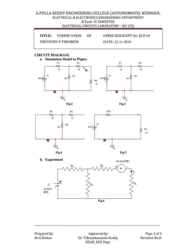
CIRCUIT DIAGRAM:
a. Simulation Model in PSpice R1
10
V1
30Vdc
0
0V
I
R3
15
R6
10
R5
20
V1
30Vdc
R1
10
0
R5
20
0V
R3
15
Fig.2 Fig.3
0
0V
R5
20
R1
10
R3
15
V1
VTH
0
RTH
R6
10
0V
Fig.4 Fig.5
b. Experiment
Fig.6
(0-30)V
RPS
(0-2)A/MC

G.PULLA REDDY ENGINEERING COLLEGE (AUTONOMOUS): KURNOOL ELECTRICAL & ELECTRONICS ENGINEERING DEPARTMENT
B.Tech- IV SEMESTER
ELECTRICAL CIRCUITS LABORATORY - (EC (P))
-----------------------------------------------------------------------------------------------------------
Prepared by Approved by Page 4 of 5
Dr.G.Kishor Dr. T.Bramhananda Reddy Revision No.0
HEAD, EEE Dept.
TITLE: VERIFICATION OF
THEVENIN’S THEOREM
GPREC/EEE/EXPT.No. ECP-04
DATE: 22-11-2018
Fig.7
Fig.8
Fig.9
TABULAR COLUMN:
Table.1 for Fig.6 Table.2 for Fig.7
S.No. V
(V)
IL(A)
Th. Pr.
S.No. V(V)
VTH(V)
Th. Pr.
(0-2)A/MC
(0-30)V
RPS

G.PULLA REDDY ENGINEERING COLLEGE (AUTONOMOUS): KURNOOL ELECTRICAL & ELECTRONICS ENGINEERING DEPARTMENT
B.Tech- IV SEMESTER
ELECTRICAL CIRCUITS LABORATORY - (EC (P))
-----------------------------------------------------------------------------------------------------------
Prepared by Approved by Page 5 of 5
Dr.G.Kishor Dr. T.Bramhananda Reddy Revision No.0
HEAD, EEE Dept.
TITLE: VERIFICATION OF
THEVENIN’S THEOREM
GPREC/EEE/EXPT.No. ECP-04
DATE: 22-11-2018
Table.3 for Fig.8 Table.4 for Fig.9
PROCEDURE:
1. a. Connections are made as per the circuit shown in Fig.6.
b. By varying the voltage in steps note down the readings.
2. a. Connections are made as per the circuit shown in Fig.7.
b. By varying the voltage in steps note down the readings.
3. Connections are made as per the circuit shown in Fig. 8 to find RTH.
4. a. Connections are made as per the circuit shown in Fig. 9.
b. Vary the voltage in steps of VTH and note down the readings of IL’.
The above procedure is followed for experiment also.
RESULT: Thevenin’s theorem is verified.
QUESTIONS:
1. Define Thevenins theorem
2. What are the applications of Thevenins theorem.
3. Explain the procedure of solving the circuits using Thevenins theorem.
4. Draw the equivalent circuit of Thevenin’s theorem.
5. State the difference between Thevenin’s and Norton’s theorem?
RTH(Ω)
Sl.no. VTH(V)
IL’(A)
Th. Pr.

G.PULLA REDDY ENGINEERING COLLEGE (AUTONOMOUS): KURNOOL ELECTRICAL & ELECTRONICS ENGINEERING DEPARTMENT
B.Tech- IV SEMESTER
ELECTRICAL CIRCUITS LABORATORY - (EC (P))
------------------------------------------------------------------------------------------------------------
Prepared by Approved by Page 1 of 5
Dr. G.Kishor Dr. T.Bramhananda Reddy Revision No.0
HEAD, EEE Dept.
TITLE: VERIFICATION OF
NORTON’S THEOREM
GPRECD/EEE/EXPT.No.ECP-05
DATE: 22-11-2018
OBJECTIVE: To verify Norton’s theorem by (a) Experiment (b) Simulation in PSpice
software.
APPARATUS:
Sl.No. Unit Range Type No.
1 Regulated power supply (0-30)V/(0-2)A 2
2 Rheostat 4
3 Digital multimeter 1
4 Ammeter (0-2)A MC 1
5 Connecting Wires Reqd.
NORTON’S THEOREM:
STATEMENT: Norton’s Theorem states that any two terminal linear network with
current sources, voltage sources and resistances can be replaced by an equivalent circuit
consisting of a current source in parallel with a resistance. The value of the current
source is that short circuit current between the two terminals of the network and the
resistance is the equivalent resistance measured between the terminals of the network
with all the energy sources replaced by their internal resistance.
Fig. Norton’s Equivalent Circuit
THEORY: This theorem is just alternative of Thevenin theorem.
G.PULLA REDDY ENGINEERING COLLEGE (AUTONOMOUS): KURNOOL ELECTRICAL & ELECTRONICS ENGINEERING DEPARTMENT
B.Tech- IV SEMESTER
ELECTRICAL CIRCUITS LABORATORY - (EC (P))
------------------------------------------------------------------------------------------------------------
Prepared by Approved by Page 2 of 5
Dr. G.Kishor Dr. T.Bramhananda Reddy Revision No.0
HEAD, EEE Dept.
TITLE: VERIFICATION OF
NORTON’S THEOREM
GPRECD/EEE/EXPT.No.ECP-05
DATE: 22-11-2018
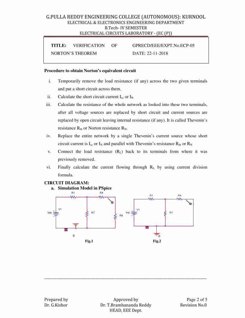
Procedure to obtain Norton’s equivalent circuit
i. Temporarily remove the load resistance (if any) across the two given terminals
and put a short circuit across them.
ii. Calculate the short circuit current Isc or IN
iii. Calculate the resistance of the whole network as looked into these two terminals,
after all voltage sources are replaced by short circuit and current sources are
replaced by open circuit leaving internal resistance (if any). It is called Thevenin’s
resistance Rth or Norton resistance RN.
iv. Replace the entire network by a single Thevenin’s current source whose short
circuit current is Isc or IN and parallel with Thevenin’s resistance Rth or RN
v. Connect the load resistance (RL) back to its terminals from where it was
previously removed.
vi. Finally calculate the current flowing through RL by using current division
formula.
CIRCUIT DIAGRAM:
a. Simulation Model in PSpice
0V
R1
I
R7
V1
Vdc
R6
R4
0
R7
R1
I
V1
Vdc
R4
0
0V
Fig.1 Fig.2
G.PULLA REDDY ENGINEERING COLLEGE (AUTONOMOUS): KURNOOL ELECTRICAL & ELECTRONICS ENGINEERING DEPARTMENT
B.Tech- IV SEMESTER
ELECTRICAL CIRCUITS LABORATORY - (EC (P))
------------------------------------------------------------------------------------------------------------
Prepared by Approved by Page 3 of 5
Dr. G.Kishor Dr. T.Bramhananda Reddy Revision No.0
HEAD, EEE Dept.
TITLE: VERIFICATION OF
NORTON’S THEOREM
GPRECD/EEE/EXPT.No.ECP-05
DATE: 22-11-2018
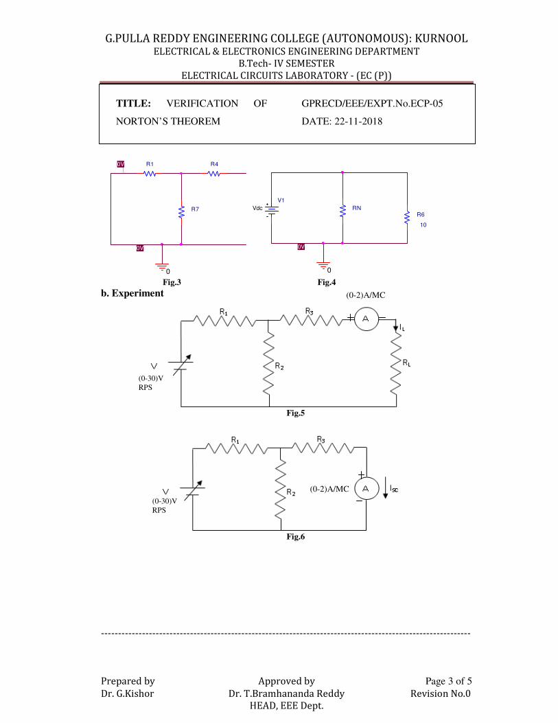
0
R7
0V
R4R10V
0
RN
V1
Vdc
R6
10
0V
Fig.3 Fig.4
b. Experiment
Fig.5
Fig.6
(0-30)V
RPS
(0-30)V
RPS
(0-2)A/MC
(0-2)A/MC
G.PULLA REDDY ENGINEERING COLLEGE (AUTONOMOUS): KURNOOL ELECTRICAL & ELECTRONICS ENGINEERING DEPARTMENT
B.Tech- IV SEMESTER
ELECTRICAL CIRCUITS LABORATORY - (EC (P))
------------------------------------------------------------------------------------------------------------
Prepared by Approved by Page 4 of 5
Dr. G.Kishor Dr. T.Bramhananda Reddy Revision No.0
HEAD, EEE Dept.
TITLE: VERIFICATION OF
NORTON’S THEOREM
GPRECD/EEE/EXPT.No.ECP-05
DATE: 22-11-2018
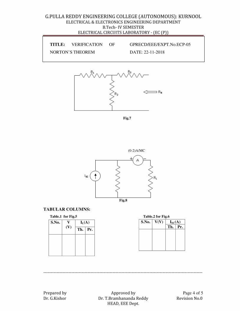
Fig.7
Fig.8
TABULAR COLUMNS:
Table.1 for Fig.5
Table.2 for Fig.6
S.No. V
(V)
IL(A)
Th. Pr.
S.No. V(V)
ISC(A)
Th. Pr.
(0-2)A/MC
G.PULLA REDDY ENGINEERING COLLEGE (AUTONOMOUS): KURNOOL ELECTRICAL & ELECTRONICS ENGINEERING DEPARTMENT
B.Tech- IV SEMESTER
ELECTRICAL CIRCUITS LABORATORY - (EC (P))
------------------------------------------------------------------------------------------------------------
Prepared by Approved by Page 5 of 5
Dr. G.Kishor Dr. T.Bramhananda Reddy Revision No.0
HEAD, EEE Dept.
TITLE: VERIFICATION OF
NORTON’S THEOREM
GPRECD/EEE/EXPT.No.ECP-05
DATE: 22-11-2018
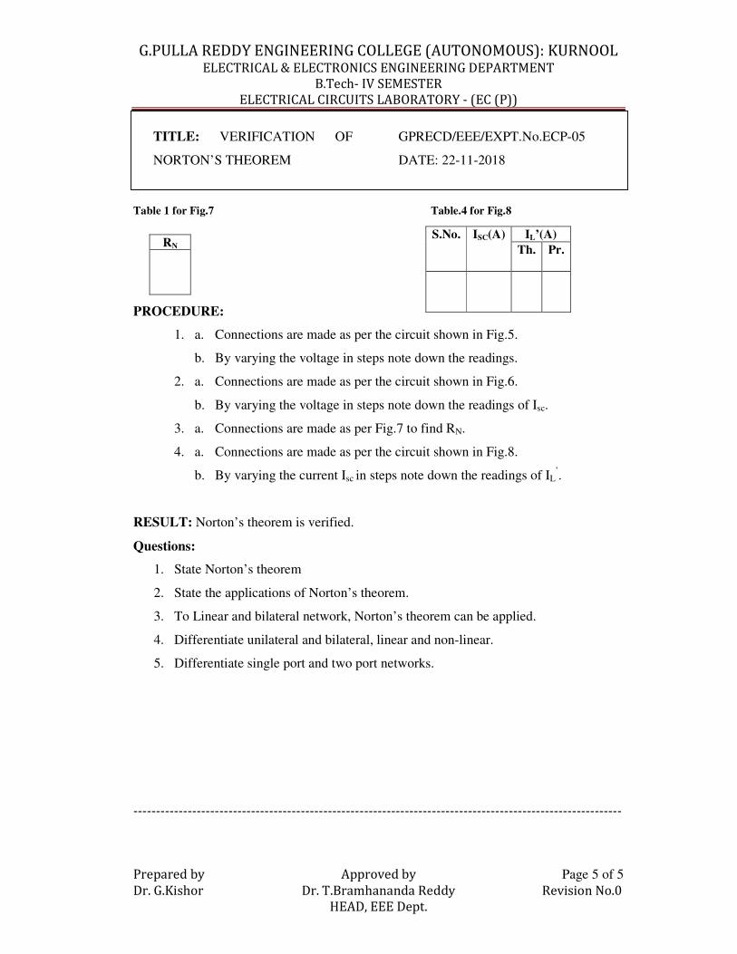
Table 1 for Fig.7 Table.4 for Fig.8
PROCEDURE:
1. a. Connections are made as per the circuit shown in Fig.5.
b. By varying the voltage in steps note down the readings.
2. a. Connections are made as per the circuit shown in Fig.6.
b. By varying the voltage in steps note down the readings of Isc.
3. a. Connections are made as per Fig.7 to find RN.
4. a. Connections are made as per the circuit shown in Fig.8.
b. By varying the current Isc in steps note down the readings of IL’.
RESULT: Norton’s theorem is verified.
Questions:
1. State Norton’s theorem
2. State the applications of Norton’s theorem.
3. To Linear and bilateral network, Norton’s theorem can be applied.
4. Differentiate unilateral and bilateral, linear and non-linear.
5. Differentiate single port and two port networks.
S.No. ISC(A)
IL’(A)
Th.
Pr.
RN
G.PULLA REDDY ENGINEERING COLLEGE (AUTONOMOUS): KURNOOL ELECTRICAL & ELECTRONICS ENGINEERING DEPARTMENT
B.Tech- IV SEMESTER
ELECTRICAL CIRCUITS LABORATORY - (EC (P))
------------------------------------------------------------------------------------------------------------
Prepared by Approved by Page 1 of 6
Dr.G.Kishor Dr. T.Bramhananda Reddy Revision No.0
HEAD, EEE Dept.
TITLE: DETERMINATION OF
SELF & MUTUAL
INDUCTANCE
GPREC/EEE/EXPT.No. EC(P)-06
DATE: 22-11-2018
OBJECTIVE: To Determine of Self Inductance, Mutual Inductance and coefficient of
coupling of an air core transformer.
APPARATUS:
Sl.No. Unit Range Type No.
1 Air core transformer 1KVA 1
2 Ammeter 0-5A MI 1
3 Voltmeter 0-300V MI 1
4 Wattmeter 5A, 300V LPF
UPF
1
1
5 Connecting Wires Reqd.
THEORY:
Self Inductance:
The property of self-inductance is a particular form of electromagnetic induction. Self
inductance is defined as the induction of a voltage in a current-carrying wire when the
current in the wire itself is changing. In the case of self-inductance, the magnetic field
created by a changing current in the circuit itself induces a voltage in the same circuit.
Therefore, the voltage is self-induced.
From the concepts of basic electrical engineering, we know that inductance may also be
expressed as
Therefore self inductance is represented as

G.PULLA REDDY ENGINEERING COLLEGE (AUTONOMOUS): KURNOOL ELECTRICAL & ELECTRONICS ENGINEERING DEPARTMENT
B.Tech- IV SEMESTER
ELECTRICAL CIRCUITS LABORATORY - (EC (P))
------------------------------------------------------------------------------------------------------------
Prepared by Approved by Page 2 of 6
Dr.G.Kishor Dr. T.Bramhananda Reddy Revision No.0
HEAD, EEE Dept.
TITLE: DETERMINATION OF
SELF & MUTUAL
INDUCTANCE
GPREC/EEE/EXPT.No. EC(P)-06
DATE: 22-11-2018
The unit for self inductance is Henry.
Mutual Inductance:
Mutual inductance is defined as the constant of proportionality between the rate of
change in current in one circuit and the resulting e.m.f induced in another circuit. A
varying current in coil 1 produces a magnetic field. This magnetic field links with coil 2
and inducing an e.m.f between its ends. Such an action in which a varying quantity in one
circuit causes the development of a quantity in a different circuit is called mutual action
or transfer action. Figure shows two coils which carry current I1 and I2. The coils will
have leakage flux Φ11 and Φ22 for coils 1 and coil 2, respectively, and a mutual flux Φ21
where the flux of coil 2 links coil 1 or flux of coil 1 links coil 2. The induced voltage of
coil 2 may be written as
Fig. 1
As Φ12 is related to current of coil 1, the induced voltage is proportional to the rate of
change of I1. This implies

G.PULLA REDDY ENGINEERING COLLEGE (AUTONOMOUS): KURNOOL ELECTRICAL & ELECTRONICS ENGINEERING DEPARTMENT
B.Tech- IV SEMESTER
ELECTRICAL CIRCUITS LABORATORY - (EC (P))
------------------------------------------------------------------------------------------------------------
Prepared by Approved by Page 3 of 6
Dr.G.Kishor Dr. T.Bramhananda Reddy Revision No.0
HEAD, EEE Dept.
TITLE: DETERMINATION OF
SELF & MUTUAL
INDUCTANCE
GPREC/EEE/EXPT.No. EC(P)-06
DATE: 22-11-2018
where M is constant of proportionality between the two coils, also known as mutual
inductance.
When the coils are linked with air as medium, the flux and current are linearly
proportional to each other and the expressions of mutual inductance are written as
Coefficient of Coupling
Coefficient of coupling is defined as the ratio of mutual inductance actually present
between the two coils to the maximum possible value.
Where
K is the coupling coefficient and 0≤ k ≤ 1
L1 is the inductance of the first coil, and
L2 is the inductance of the second coil.
G.PULLA REDDY ENGINEERING COLLEGE (AUTONOMOUS): KURNOOL ELECTRICAL & ELECTRONICS ENGINEERING DEPARTMENT
B.Tech- IV SEMESTER
ELECTRICAL CIRCUITS LABORATORY - (EC (P))
------------------------------------------------------------------------------------------------------------
Prepared by Approved by Page 4 of 6
Dr.G.Kishor Dr. T.Bramhananda Reddy Revision No.0
HEAD, EEE Dept.
TITLE: DETERMINATION OF
SELF & MUTUAL
INDUCTANCE
GPREC/EEE/EXPT.No. EC(P)-06
DATE: 22-11-2018
CIRCUIT DIAGRAM:
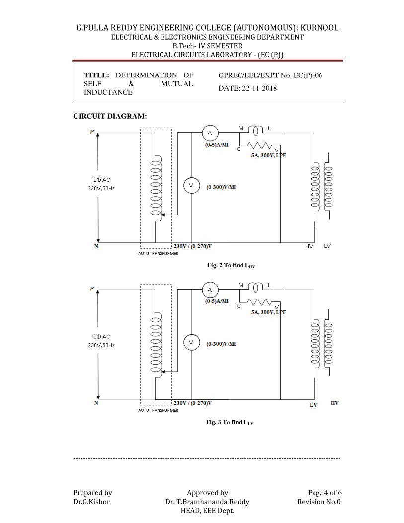
Fig. 2 To find LHV
Fig. 3 To find LLV
G.PULLA REDDY ENGINEERING COLLEGE (AUTONOMOUS): KURNOOL ELECTRICAL & ELECTRONICS ENGINEERING DEPARTMENT
B.Tech- IV SEMESTER
ELECTRICAL CIRCUITS LABORATORY - (EC (P))
------------------------------------------------------------------------------------------------------------
Prepared by Approved by Page 5 of 6
Dr.G.Kishor Dr. T.Bramhananda Reddy Revision No.0
HEAD, EEE Dept.
TITLE: DETERMINATION OF
SELF & MUTUAL
INDUCTANCE
GPREC/EEE/EXPT.No. EC(P)-06
DATE: 22-11-2018
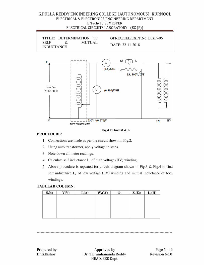
Fig.4 To find M & K
PROCEDURE:
1. Connections are made as per the circuit shown in Fig.2.
2. Using auto transformer, apply voltage in steps.
3. Note down all meter readings.
4. Calculate self inductance L1 of high voltage (HV) winding.
5. Above procedure is repeated for circuit diagram shown in Fig.3 & Fig.4 to find
self inductance L2 of low voltage (LV) winding and mutual inductance of both
windings.
TABULAR COLUMN:
S.No V(V) I1(A) W1(W) Φ1 Z1(Ω) L1(H)

G.PULLA REDDY ENGINEERING COLLEGE (AUTONOMOUS): KURNOOL ELECTRICAL & ELECTRONICS ENGINEERING DEPARTMENT
B.Tech- IV SEMESTER
ELECTRICAL CIRCUITS LABORATORY - (EC (P))
------------------------------------------------------------------------------------------------------------
Prepared by Approved by Page 6 of 6
Dr.G.Kishor Dr. T.Bramhananda Reddy Revision No.0
HEAD, EEE Dept.
TITLE: DETERMINATION OF
SELF & MUTUAL
INDUCTANCE
GPREC/EEE/EXPT.No. EC(P)-06
DATE: 22-11-2018
Sl.No V(V) I2(A) W2(W) Φ2 Z2(Ω) L2(H)
Sl.No V(V) I(A) W(W) Φ Z(Ω) L(H) M=(L-(L1+L2))/2
RESULT: Self inductance, mutual inductance and coefficient of coupling are
determined.
Questions:
1. Define self inductance.
2. Define mutual inductance.
3. Define coefficient of coupling.
4. Differentiate air core and iron core transformer.
5. If the transformer core is made of wood, what will be the coupling coefficient.

G.PULLA REDDY ENGINEERING COLLEGE (AUTONOMOUS): KURNOOL ELECTRICAL & ELECTRONICS ENGINEERING DEPARTMENT
B.Tech- IV SEMESTER
ELECTRICAL CIRCUITS LABORATORY - (EC (P))
------------------------------------------------------------------------------------------------------------
Prepared by Approved by Page 1 of 9
Dr.G.Kishor Dr. T.Bramhananda Reddy Revision No.1
HEAD, EEE Dept.
TITLE: RLC SERIES &
PARALLEL RESONANCE
GPREC/EEE/EXPT.No. ECP-07
DATE: 22-11-2018
OBJECTIVE: To verify RLC Series resonance & Parallel resonance.
APPARATUS:
Sl.No. Unit Range Type No. Required
1 Function Generator 1
2 Digital Multimeter 1
3 Resistor 1KΩ 1
4 Capacitor 0.1µF 1
5 Inductance box 25mH 1
6 Connecting Wires Reqd.
THEORY:
In an electrical circuit consisting of various active sources and passive sources,
the state at which the current is maximum is called as resonance. In a series RLC circuit
the condition of current lagging or leading the applied voltage depends upon the values of
CL XandX . If one of the parameters of the series RLC circuit is varied in such a way
that the current in the circuit is in phase with the applied voltage, then the circuit is said
to be in resonance. In other words resonance can also be defined as when the net or total
current in an electrical circuit is in phase with the applied voltage, then the circuit is said
to undergo resonance
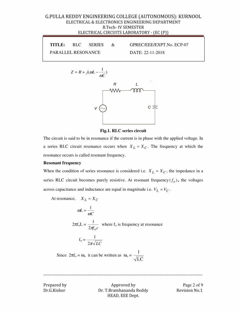
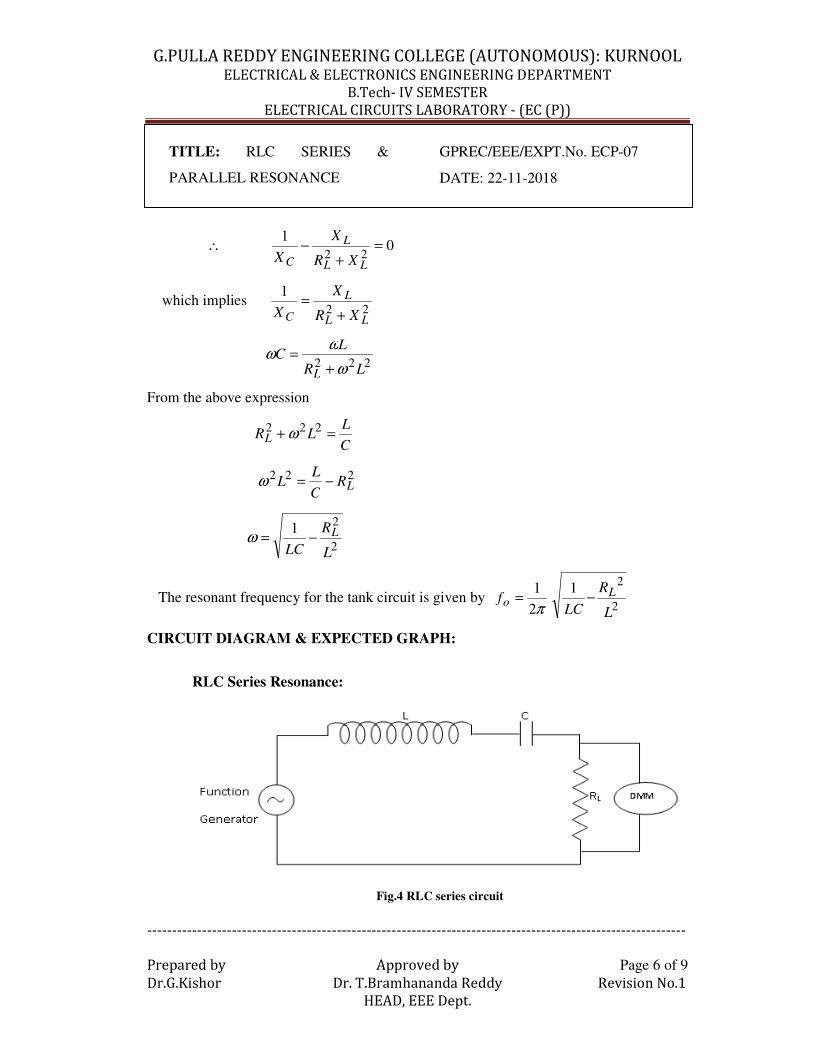
Fig.1 shows a series RLC circuit where the parameters R, L, C are laid in series with each
other. The voltage of the circuit is given by
))(( CL XXjRIV −+=
Total impedance of the series RLC circuit is given by
)( CL XXjRZ −+=
G.PULLA REDDY ENGINEERING COLLEGE (AUTONOMOUS): KURNOOL ELECTRICAL & ELECTRONICS ENGINEERING DEPARTMENT
B.Tech- IV SEMESTER
ELECTRICAL CIRCUITS LABORATORY - (EC (P))
------------------------------------------------------------------------------------------------------------
Prepared by Approved by Page 2 of 9
Dr.G.Kishor Dr. T.Bramhananda Reddy Revision No.1
HEAD, EEE Dept.
TITLE: RLC SERIES &
PARALLEL RESONANCE
GPREC/EEE/EXPT.No. ECP-07
DATE: 22-11-2018
)1
(C
LjRZω
ω −+=
Fig.1. RLC series circuit
The circuit is said to be in resonance if the current is in phase with the applied voltage. In
a series RLC circuit resonance occurs when CL XX = . The frequency at which the
resonance occurs is called resonant frequency.
Resonant frequency
When the condition of series resonance is considered i.e. CL XX = , the impedance in a
series RLC circuit becomes purely resistive. At resonant frequency )( of , the voltages
across capacitance and inductance are equal in magnitude i.e. CL VV = .
At resonance, CL XX =
C
Lω
ω1
=
2πfoL = cfoπ2
1 where fo is frequency at resonance
fo = LCπ2
1
Since 2πfo = ωo it can be written as ωo = LC
1
G.PULLA REDDY ENGINEERING COLLEGE (AUTONOMOUS): KURNOOL ELECTRICAL & ELECTRONICS ENGINEERING DEPARTMENT
B.Tech- IV SEMESTER
ELECTRICAL CIRCUITS LABORATORY - (EC (P))
------------------------------------------------------------------------------------------------------------
Prepared by Approved by Page 3 of 9
Dr.G.Kishor Dr. T.Bramhananda Reddy Revision No.1
HEAD, EEE Dept.
TITLE: RLC SERIES &
PARALLEL RESONANCE
GPREC/EEE/EXPT.No. ECP-07
DATE: 22-11-2018
The relation of resonant frequency changes when the R-L-C parameters are placed in
parallel with each other. Two cases are majorly considered in the concept of parallel
resonance.
i. Considering the internal resistance of both L and C
ii. Considering the internal resistance of only L
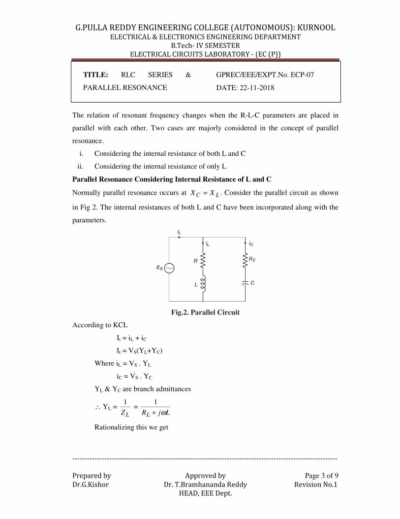
Parallel Resonance Considering Internal Resistance of L and C
Normally parallel resonance occurs at LC XX = . Consider the parallel circuit as shown
in Fig 2. The internal resistances of both L and C have been incorporated along with the
parameters.
Fig.2. Parallel Circuit
According to KCL
It = iL + iC
It = VS(YL+YC)
Where iL = VS . YL
iC = VS . YC
YL & YC are branch admittances
∴ YL = LZ
1 =
LjRL ω+
1
Rationalizing this we get
G.PULLA REDDY ENGINEERING COLLEGE (AUTONOMOUS): KURNOOL ELECTRICAL & ELECTRONICS ENGINEERING DEPARTMENT
B.Tech- IV SEMESTER
ELECTRICAL CIRCUITS LABORATORY - (EC (P))
------------------------------------------------------------------------------------------------------------
Prepared by Approved by Page 4 of 9
Dr.G.Kishor Dr. T.Bramhananda Reddy Revision No.1
HEAD, EEE Dept.
TITLE: RLC SERIES &
PARALLEL RESONANCE
GPREC/EEE/EXPT.No. ECP-07
DATE: 22-11-2018
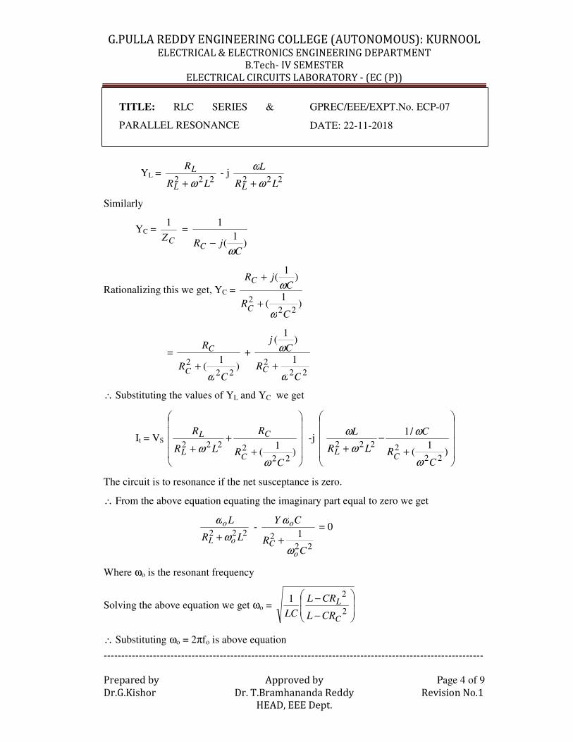
YL = 222
LR
R
L
L
ω+
- j 222
LR
L
L ω
ω
+
Similarly
YC = CZ
1 =
)1
(
1
CjRC
ω−
Rationalizing this we get, YC =
)1
(
)1
(
22
2
CR
CjR
C
C
ω
ω
+
+
=
)1
(22
2
CR
R
C
C
ω+
+
22
2 1
)1
(
CR
Cj
Cω
ω
+
∴ Substituting the values of YL and YC we get
It = VS
+
+
+ )1
(22
2222
CR
R
LR
R
C
C
L
L
ω
ω
-j
+
−
+ )1
(
/1
22
2222
CR
C
LR
L
CL
ω
ω
ω
ω
The circuit is to resonance if the net susceptance is zero.
∴ From the above equation equating the imaginary part equal to zero we get
222
LR
L
oL
o
ω
ω
+
-
22
2 1
CR
CY
o
C
o
ω
ω
+
= 0
Where ωo is the resonant frequency
Solving the above equation we get ωo =
−
−
2
21
C
L
CRL
CRL
LC
∴ Substituting ωo = 2πfo is above equation
G.PULLA REDDY ENGINEERING COLLEGE (AUTONOMOUS): KURNOOL ELECTRICAL & ELECTRONICS ENGINEERING DEPARTMENT
B.Tech- IV SEMESTER
ELECTRICAL CIRCUITS LABORATORY - (EC (P))
------------------------------------------------------------------------------------------------------------
Prepared by Approved by Page 5 of 9
Dr.G.Kishor Dr. T.Bramhananda Reddy Revision No.1
HEAD, EEE Dept.
TITLE: RLC SERIES &
PARALLEL RESONANCE
GPREC/EEE/EXPT.No. ECP-07
DATE: 22-11-2018
fo = π2
1
−
−
2
21
C
L
CRL
CRL
LC
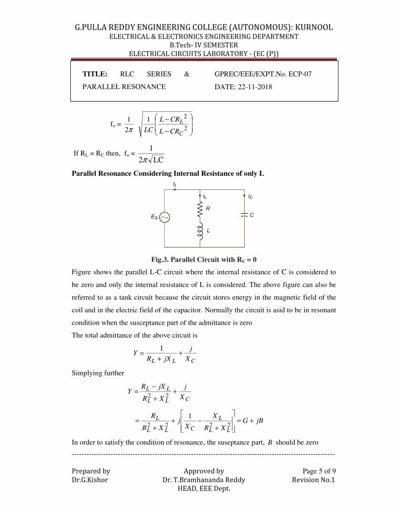
If RL = RC then, fo = LC2
1
π
Parallel Resonance Considering Internal Resistance of only L
Fig.3. Parallel Circuit with RC = 0
Figure shows the parallel L-C circuit where the internal resistance of C is considered to
be zero and only the internal resistance of L is considered. The above figure can also be
referred to as a tank circuit because the circuit stores energy in the magnetic field of the
coil and in the electric field of the capacitor. Normally the circuit is asid to be in resonant
condition when the susceptance part of the admittance is zero
The total admittance of the above circuit is
CLL X
j
jXRY +
+=
1
Simplying further
CLL
LL
X
j
XR
jXRY +
+
−=
22
jBGXR
X
Xj
XR
R
LL
L
CLL
L+=
+
−+
+
=2222
1
In order to satisfy the condition of resonance, the suseptance part, B should be zero
G.PULLA REDDY ENGINEERING COLLEGE (AUTONOMOUS): KURNOOL ELECTRICAL & ELECTRONICS ENGINEERING DEPARTMENT
B.Tech- IV SEMESTER
ELECTRICAL CIRCUITS LABORATORY - (EC (P))
------------------------------------------------------------------------------------------------------------
Prepared by Approved by Page 6 of 9
Dr.G.Kishor Dr. T.Bramhananda Reddy Revision No.1
HEAD, EEE Dept.
TITLE: RLC SERIES &
PARALLEL RESONANCE
GPREC/EEE/EXPT.No. ECP-07
DATE: 22-11-2018
∴ 01
22=
+
−
LL
L
C XR
X
X
which implies 22
1
LL
L
C XR
X
X +
=
222 LR
LC
L ω
ωω
+
=
From the above expression
C
LLRL =+
222ω
222LR
C
LL −=ω
2
21
L
R
LC
L−=ω
The resonant frequency for the tank circuit is given by π2
1=of 2
21
L
R
LC
L−
CIRCUIT DIAGRAM & EXPECTED GRAPH:
RLC Series Resonance:
Fig.4 RLC series circuit

G.PULLA REDDY ENGINEERING COLLEGE (AUTONOMOUS): KURNOOL ELECTRICAL & ELECTRONICS ENGINEERING DEPARTMENT
B.Tech- IV SEMESTER
ELECTRICAL CIRCUITS LABORATORY - (EC (P))
------------------------------------------------------------------------------------------------------------
Prepared by Approved by Page 7 of 9
Dr.G.Kishor Dr. T.Bramhananda Reddy Revision No.1
HEAD, EEE Dept.
TITLE: RLC SERIES &
PARALLEL RESONANCE
GPREC/EEE/EXPT.No. ECP-07
DATE: 22-11-2018
RLC Parallel Resonance:
Fig.5 RLC Parallel Circuit
G.PULLA REDDY ENGINEERING COLLEGE (AUTONOMOUS): KURNOOL ELECTRICAL & ELECTRONICS ENGINEERING DEPARTMENT
B.Tech- IV SEMESTER
ELECTRICAL CIRCUITS LABORATORY - (EC (P))
------------------------------------------------------------------------------------------------------------
Prepared by Approved by Page 8 of 9
Dr.G.Kishor Dr. T.Bramhananda Reddy Revision No.1
HEAD, EEE Dept.
TITLE: RLC SERIES &
PARALLEL RESONANCE
GPREC/EEE/EXPT.No. ECP-07
DATE: 22-11-2018
PROCEDURE:
RLC Series & Parallel Resonance:
1. Connections are made as per the circuit diagram shown in Fig.4 & Fig.5, for
series and parallel resonance respectively.
2. By varying the frequency of the function generator, note down the voltmeter
reading.
3. Find the current I by using R value
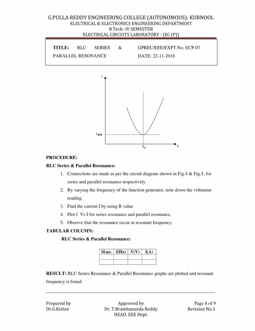
4. Plot f Vs I for series resonance and parallel resonance.
5. Observe that the resonance occur at resonant frequency.
TABULAR COLUMN:
RLC Series & Parallel Resonance:
RESULT: RLC Series Resonance & Parallel Resonance graphs are plotted and resonant
frequency is found.
Sl.no. f(Hz) V(V) I(A)

G.PULLA REDDY ENGINEERING COLLEGE (AUTONOMOUS): KURNOOL ELECTRICAL & ELECTRONICS ENGINEERING DEPARTMENT
B.Tech- IV SEMESTER
ELECTRICAL CIRCUITS LABORATORY - (EC (P))
------------------------------------------------------------------------------------------------------------
Prepared by Approved by Page 9 of 9
Dr.G.Kishor Dr. T.Bramhananda Reddy Revision No.1
HEAD, EEE Dept.
TITLE: RLC SERIES &
PARALLEL RESONANCE
GPREC/EEE/EXPT.No. ECP-07
DATE: 22-11-2018
Questions:
1. Define resonance.
2. What is the condition for resonance in RLC series and parallel circuits.
3. Define bandwidth
4. Define Selectivity
5. Define Q factor.
G.PULLA REDDY ENGINEERING COLLEGE (AUTONOMOUS): KURNOOL ELECTRICAL & ELECTRONICS ENGINEERING DEPARTMENT
B.Tech- IV SEMESTER
ELECTRICAL CIRCUITS LABORATORY - (EC (P))
------------------------------------------------------------------------------------------------------------
Prepared by Approved by Page 1 of 8
Dr.G.Kishor Dr. T.Bramhananda Reddy Revision No.0
HEAD, EEE Dept.
TITLE: DETERMINATION OF Z
& Y PARAMETERS
GPREC/EEE/EXPT.No. ECP-08
DATE: 22-11-2018
OBJECTIVE: To determine Impedance (Z) & Admittance (Y) parameters.
APPARATUS:
Sl.No. Unit Range Type No.
1 Regulated power supply (0-30) V/(0-2)A 1
2 Rheostats -
3 Voltmeter (0-30) V MC 2
4 Ammeter (0-2)A MC 2
5 Connecting Wires Reqd.
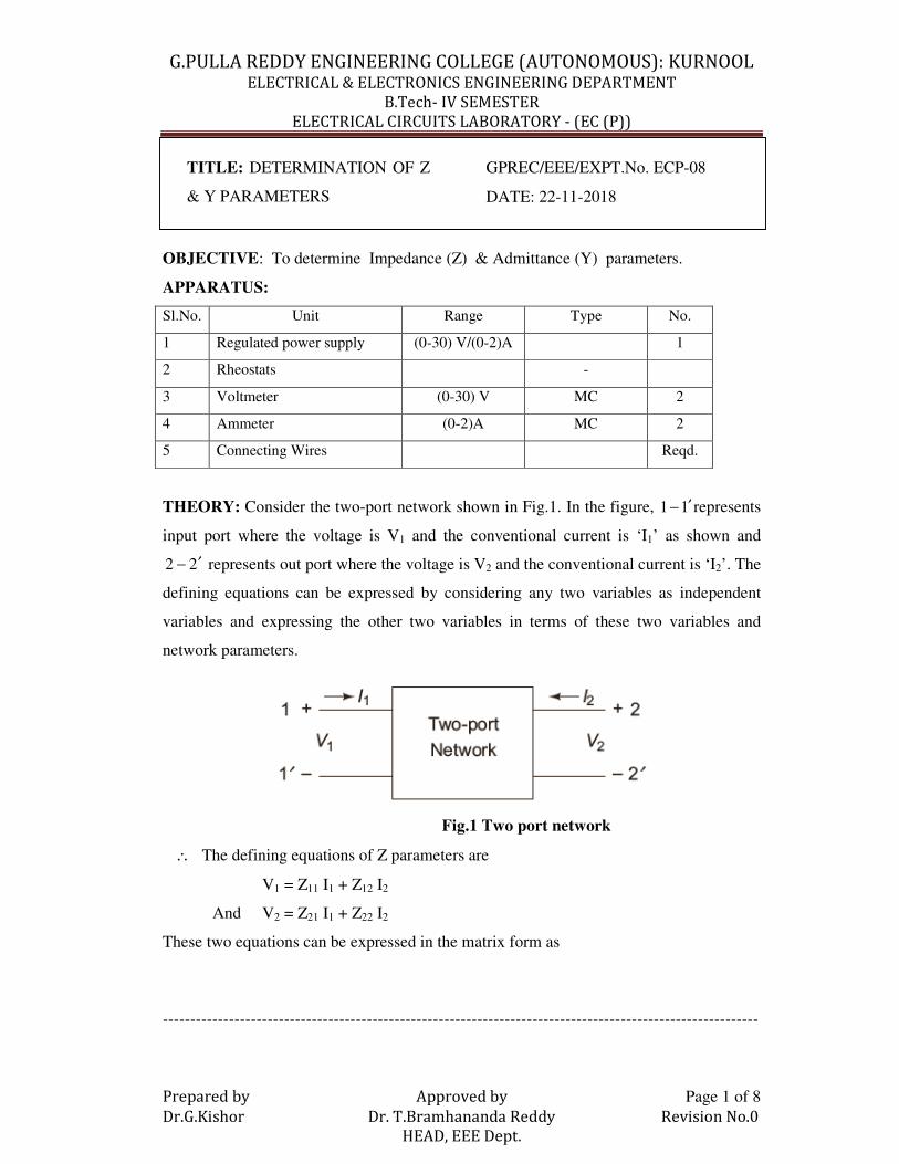
THEORY: Consider the two-port network shown in Fig.1. In the figure, 11 ′− represents
input port where the voltage is V1 and the conventional current is ‘I1’ as shown and
22 ′− represents out port where the voltage is V2 and the conventional current is ‘I2’. The
defining equations can be expressed by considering any two variables as independent
variables and expressing the other two variables in terms of these two variables and
network parameters.
Fig.1 Two port network
∴ The defining equations of Z parameters are
V1 = Z11 I1 + Z12 I2
And V2 = Z21 I1 + Z22 I2
These two equations can be expressed in the matrix form as
G.PULLA REDDY ENGINEERING COLLEGE (AUTONOMOUS): KURNOOL ELECTRICAL & ELECTRONICS ENGINEERING DEPARTMENT
B.Tech- IV SEMESTER
ELECTRICAL CIRCUITS LABORATORY - (EC (P))
------------------------------------------------------------------------------------------------------------
Prepared by Approved by Page 2 of 8
Dr.G.Kishor Dr. T.Bramhananda Reddy Revision No.0
HEAD, EEE Dept.
TITLE: DETERMINATION OF Z
& Y PARAMETERS
GPREC/EEE/EXPT.No. ECP-08
DATE: 22-11-2018
2
1
V
V =
2221
1211
ZZ
ZZ
2
1
I
I
Where Z11, Z12, Z21, Z22 are network parameters called Z parameters, I1 and I2 are
independent variables, V1 and V2 are dependent variables. If the output port 22 ′− is
open circuited then I2 = 0
∴ V1 = Z11 I1 + 0
⇒ Z11 = 021
1=I
I
V
Z11 is called as driving point impedance because current I1 develops voltage V1 at the
input port. Also we have
V2 = Z21 I1 + 0
⇒ Z21 = 021
2=I
I
V
Z21 is called as “Forward transfer impedance” because current I1 develops voltage V2 at
the open circuited port. Similarly Z12 and Z22 can be found by considering I1 = 0 i.e., by
open circuiting the input port terminals.
By substituting I1 = 0, we get
V1 = 0 + Z12 I2
⇒ Z12 = 012
1=I
I
V
Z12 is called as “Reverse Transfer impedance” because current I2 develops voltage V1 at
the open circuited port. Also we have
V2 = 0 + Z22 I2
⇒ Z22 = 012
2=I
I
V
Z22 is called as driving point impedance.
G.PULLA REDDY ENGINEERING COLLEGE (AUTONOMOUS): KURNOOL ELECTRICAL & ELECTRONICS ENGINEERING DEPARTMENT
B.Tech- IV SEMESTER
ELECTRICAL CIRCUITS LABORATORY - (EC (P))
------------------------------------------------------------------------------------------------------------
Prepared by Approved by Page 3 of 8
Dr.G.Kishor Dr. T.Bramhananda Reddy Revision No.0
HEAD, EEE Dept.
TITLE: DETERMINATION OF Z
& Y PARAMETERS
GPREC/EEE/EXPT.No. ECP-08
DATE: 22-11-2018
Note: The unit for Z parameters is Ohms(Ω)
Methods of finding the Z – PARAMETERS:
The defining equations for Z Parameters are
V1 = Z11 I1 + Z12 I2
V2 = Z21 I1 + Z22 I2
There are two methods for finding Z – parameters (i) Direct method and (ii) Indirect
method
(i)Direct Method
Step (i) :By open circuiting of the output port, I2 will tends to zero and so express V1 and
V2 in terms of I1 and calculated as
Z11 = 1
1
I
V and Z21 =
1
2
I
V
Step (ii) : By open circuiting of the input port, I1 will tends to zero and so express V1 and
V2 in terms of I2 and calculate as
Z12 = 2
1
I
V and Z22 =
2
2
I
V
(ii)Indirect Method
Using node analysis or loop analysis, expresses V1 and V2 in terms of I1 and I2 then
calculate Z parameters.
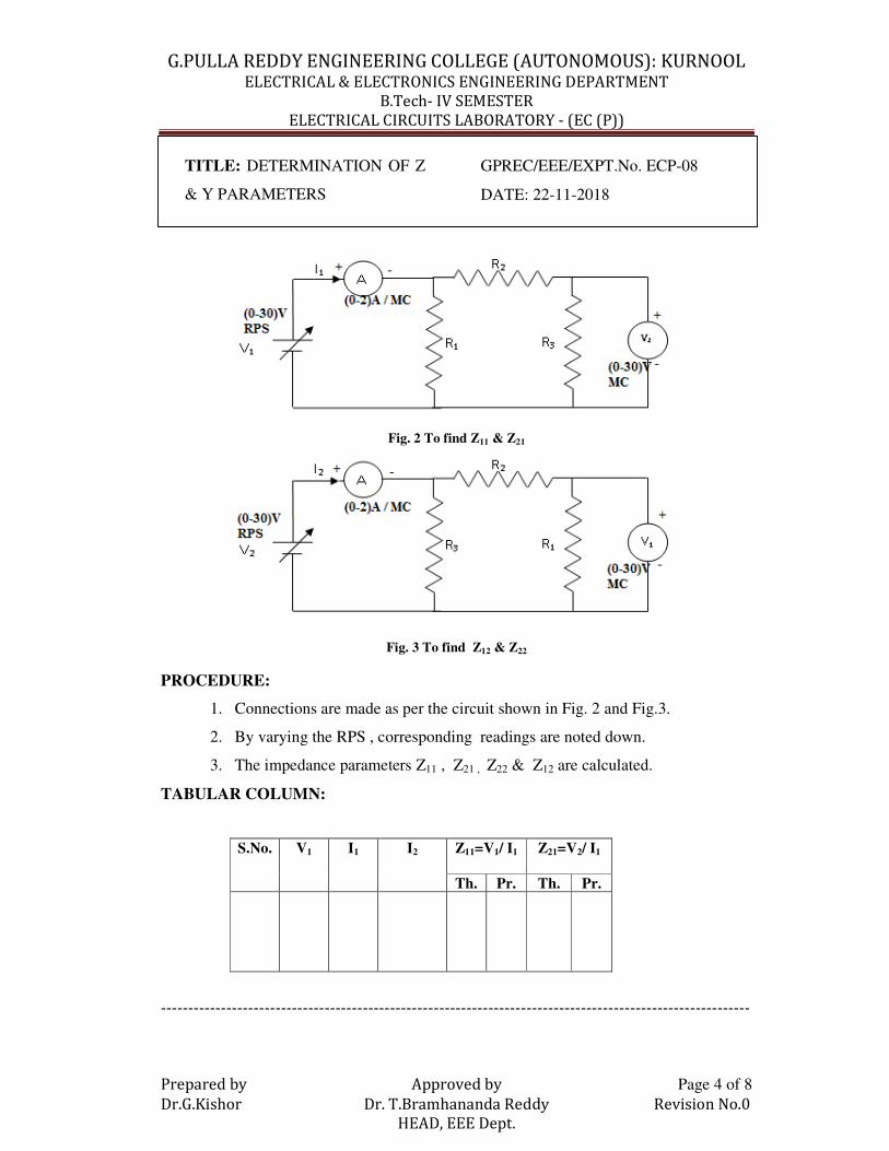
Z PARAMETERS (Open Circuit Impedance Parameters):
CIRCUIT DIAGRAM:
G.PULLA REDDY ENGINEERING COLLEGE (AUTONOMOUS): KURNOOL ELECTRICAL & ELECTRONICS ENGINEERING DEPARTMENT
B.Tech- IV SEMESTER
ELECTRICAL CIRCUITS LABORATORY - (EC (P))
------------------------------------------------------------------------------------------------------------
Prepared by Approved by Page 4 of 8
Dr.G.Kishor Dr. T.Bramhananda Reddy Revision No.0
HEAD, EEE Dept.
TITLE: DETERMINATION OF Z
& Y PARAMETERS
GPREC/EEE/EXPT.No. ECP-08
DATE: 22-11-2018
Fig. 2 To find Z11 & Z21
Fig. 3 To find Z12 & Z22
PROCEDURE:
1. Connections are made as per the circuit shown in Fig. 2 and Fig.3.
2. By varying the RPS , corresponding readings are noted down.
3. The impedance parameters Z11 , Z21 , Z22 & Z12 are calculated.
TABULAR COLUMN:
S.No. V1 I1 I2 Z11=V1/ I1
Z21=V2/ I1
Th. Pr. Th. Pr.
G.PULLA REDDY ENGINEERING COLLEGE (AUTONOMOUS): KURNOOL ELECTRICAL & ELECTRONICS ENGINEERING DEPARTMENT
B.Tech- IV SEMESTER
ELECTRICAL CIRCUITS LABORATORY - (EC (P))
------------------------------------------------------------------------------------------------------------
Prepared by Approved by Page 5 of 8
Dr.G.Kishor Dr. T.Bramhananda Reddy Revision No.0
HEAD, EEE Dept.
TITLE: DETERMINATION OF Z
& Y PARAMETERS
GPREC/EEE/EXPT.No. ECP-08
DATE: 22-11-2018
Y PARAMETERS (Short Circuit Admittance Parameters):
THEORY:
The Y-Parameters of a two port network are generally defined by expressing the port
Currents 1I and 2I in terms of their voltages 1V and 2V . The defining equations are
expressed by considering any two variables as independent variables and expressing the
other two variables in terms of these two variables and network parameters. The defining
equations for hybrid parameters are
I1 = Y11 V1 + Y12 V2
and I2 = Y21 V1 + Y22 V2
By short circuiting the output port V2 = 0
∴ I1 = Y11 V1 + 0
⇒ Y11 = 021
1=V
V
I
Y11 is called as Input admittance.
And also when V2 = 0
I2 = Y21 V1 + 0
⇒ Y21 = 021
2=V
V
I
Y21 is called as reverse transfer admittance.
S.No. V2 I1 I2 Z12=V1/ I2 Z22=V2/ I2
Th.
Pr.
Th.
Pr.
G.PULLA REDDY ENGINEERING COLLEGE (AUTONOMOUS): KURNOOL ELECTRICAL & ELECTRONICS ENGINEERING DEPARTMENT
B.Tech- IV SEMESTER
ELECTRICAL CIRCUITS LABORATORY - (EC (P))
------------------------------------------------------------------------------------------------------------
Prepared by Approved by Page 6 of 8
Dr.G.Kishor Dr. T.Bramhananda Reddy Revision No.0
HEAD, EEE Dept.
TITLE: DETERMINATION OF Z
& Y PARAMETERS
GPREC/EEE/EXPT.No. ECP-08
DATE: 22-11-2018
Similarly by short circuiting the input port V1 = 0
∴ I1 = Y12 V2
Y12 = 012
1=V
V
I
Y12 is called as Forward Transfer admittance
And also when V1 = 0
I2 = Y22 V2
⇒ Y22 = 012
2=V
V
I
Y22 is called as Output admittance
Methods of finding the Y PARAMETERS:
The defining equations for Y parameters are
I1 = Y11 V1 + Y12 V2
I2 = Y21 V1 + Y22 + V2
There are two methods for finding Y parameters (i) Direct method (ii) Indirect method
(i) Direct Method:-
Step (i) : By short circuiting the output port, V2 will tends to zero and so express I1 and I2
in terms of V1 and calculate
Y11 = 1
222
2
1 V
IYand
V
I=
Step (ii) : By short circuiting the input port, V1 will tends to zero and so express I1 and I2
in terms of V2 and calculate
Y12 = 2
222
2
1
V
IandY
V
I=
(ii) Indirect Method:-

G.PULLA REDDY ENGINEERING COLLEGE (AUTONOMOUS): KURNOOL ELECTRICAL & ELECTRONICS ENGINEERING DEPARTMENT
B.Tech- IV SEMESTER
ELECTRICAL CIRCUITS LABORATORY - (EC (P))
------------------------------------------------------------------------------------------------------------
Prepared by Approved by Page 7 of 8
Dr.G.Kishor Dr. T.Bramhananda Reddy Revision No.0
HEAD, EEE Dept.
TITLE: DETERMINATION OF Z
& Y PARAMETERS
GPREC/EEE/EXPT.No. ECP-08
DATE: 22-11-2018
Using node analysis or loop analysis express I1 and I2 in terms of V1 and V2 and then
calculate Y parameters and these are expressed in mho.
CIRCUIT DIAGRAM:
Fig. 4 To find Y11 & Y21
Fig. 5 To find Y22 & Y12
PROCEDURE:
1. Connections are to be made as per the circuit diagram shown in Fig.4.
2. Output port is short circuited and by varying V1, readings are noted down.
3. Y11 & Y21 are calculated.
4. Input port is short circuited and by varying V2 as per the circuit diagram
shown in Fig.5, readings are noted down to calculate Y22 & Y12 .
TABULAR COLUMN:

G.PULLA REDDY ENGINEERING COLLEGE (AUTONOMOUS): KURNOOL ELECTRICAL & ELECTRONICS ENGINEERING DEPARTMENT
B.Tech- IV SEMESTER
ELECTRICAL CIRCUITS LABORATORY - (EC (P))
------------------------------------------------------------------------------------------------------------
Prepared by Approved by Page 8 of 8
Dr.G.Kishor Dr. T.Bramhananda Reddy Revision No.0
HEAD, EEE Dept.
TITLE: DETERMINATION OF Z
& Y PARAMETERS
GPREC/EEE/EXPT.No. ECP-08
DATE: 22-11-2018
RESULT: Impedance and admittance parameters are determined.
Questions
1. What are the defining equations of Z and Y parameters
2. What are the conditions for symmetry
3. What are the conditions for reciprocity
4. What is the condition to be used to find Z parameters
5. What is the condition to be used to find Y parameters
S.No. V1 I1 I2 Y11=I1/V1 Y21=I2/V1
Th.
Pr.
Th.
Pr.
Sl.no. V2 I1 I2 Y12=I1/ V2 Y22=I2/V2
Th.
Pr.
Th.
Pr.
G.PULLA REDDY ENGINEERING COLLEGE (AUTONOMOUS): KURNOOL ELECTRICAL & ELECTRONICS ENGINEERING DEPARTMENT
B.Tech- IV SEMESTER
ELECTRICAL CIRCUITS LABORATORY - (EC (P))
------------------------------------------------------------------------------------------------------------
Prepared by Approved by Page 1 of 5
Dr.G.Kishor Dr. T.Bramhananda Reddy Revision No.0
HEAD, EEE Dept.
TITLE: DETERMINATION OF
ABCD PARAMETERS
GPREC/EEE/EXPT.No. ECP-09
DATE: 22-11-2018
OBJECTIVE: To Determine Transmission line parameters (ABCD)
APPARATUS:
Sl.No. Unit Range Type No.
1 Regulated Power supply (0-30) V/(0-2)A 1
2 Voltmeter (0-30) V MC 1
3 Ammeter (0-2)A MC 2
4 Rheostat 3
5 Connecting Wires Reqd.
THEORY:
ABCD-PARAMETERS
In transmission parameters the voltage and current at the sending end will be
expressed with the voltage and current at the receiving end. These parameters will be
used to study the performance of the transmission lines.
The defining equations for ABCD parameters are
V1 = AV2 – BI2
And I1 = CV2 – DI2
Here –I2 is considered because the direction of I2 is opposite to that of I1.
By open circuiting the output port, I2 = 0
∴ V1 = AV2
⇒ A = 022
1=I
V
V
A is called as open circuit voltage gain.
Also when I2 = 0
I1=CV2

G.PULLA REDDY ENGINEERING COLLEGE (AUTONOMOUS): KURNOOL ELECTRICAL & ELECTRONICS ENGINEERING DEPARTMENT
B.Tech- IV SEMESTER
ELECTRICAL CIRCUITS LABORATORY - (EC (P))
------------------------------------------------------------------------------------------------------------
Prepared by Approved by Page 2 of 5
Dr.G.Kishor Dr. T.Bramhananda Reddy Revision No.0
HEAD, EEE Dept.
TITLE: DETERMINATION OF
ABCD PARAMETERS
GPREC/EEE/EXPT.No. ECP-09
DATE: 22-11-2018
∴ C = 022
1=I
V
I
C is called as open circuit transfer impedance.
Similarly by short circuiting the out put port V2 = 0
V1 = - BI2
⇒ - B = 022
1=V
I
V
⇒ - B
1 = 02
1
2=V
V
I
It is also called as short circuit transfer admittance.
Also when V2 = 0.
I1 = - DI2
⇒ - D = 022
1=V
I
I
⇒ - D
1 = 02
1
2=V
I
I
It is also called as short circuit current gain.
Method of Finding ABCD Parameters
Transmission parameters are also known as ABCD parameters. The defining equations
for ABCD parameters are
V1 = AV2 – BI2
I1 = CV2 – Di2
1
1
I
V =
DC
BA
− 2
2
I
V
(i) Direct Method
G.PULLA REDDY ENGINEERING COLLEGE (AUTONOMOUS): KURNOOL ELECTRICAL & ELECTRONICS ENGINEERING DEPARTMENT
B.Tech- IV SEMESTER
ELECTRICAL CIRCUITS LABORATORY - (EC (P))
------------------------------------------------------------------------------------------------------------
Prepared by Approved by Page 3 of 5
Dr.G.Kishor Dr. T.Bramhananda Reddy Revision No.0
HEAD, EEE Dept.
TITLE: DETERMINATION OF
ABCD PARAMETERS
GPREC/EEE/EXPT.No. ECP-09
DATE: 22-11-2018
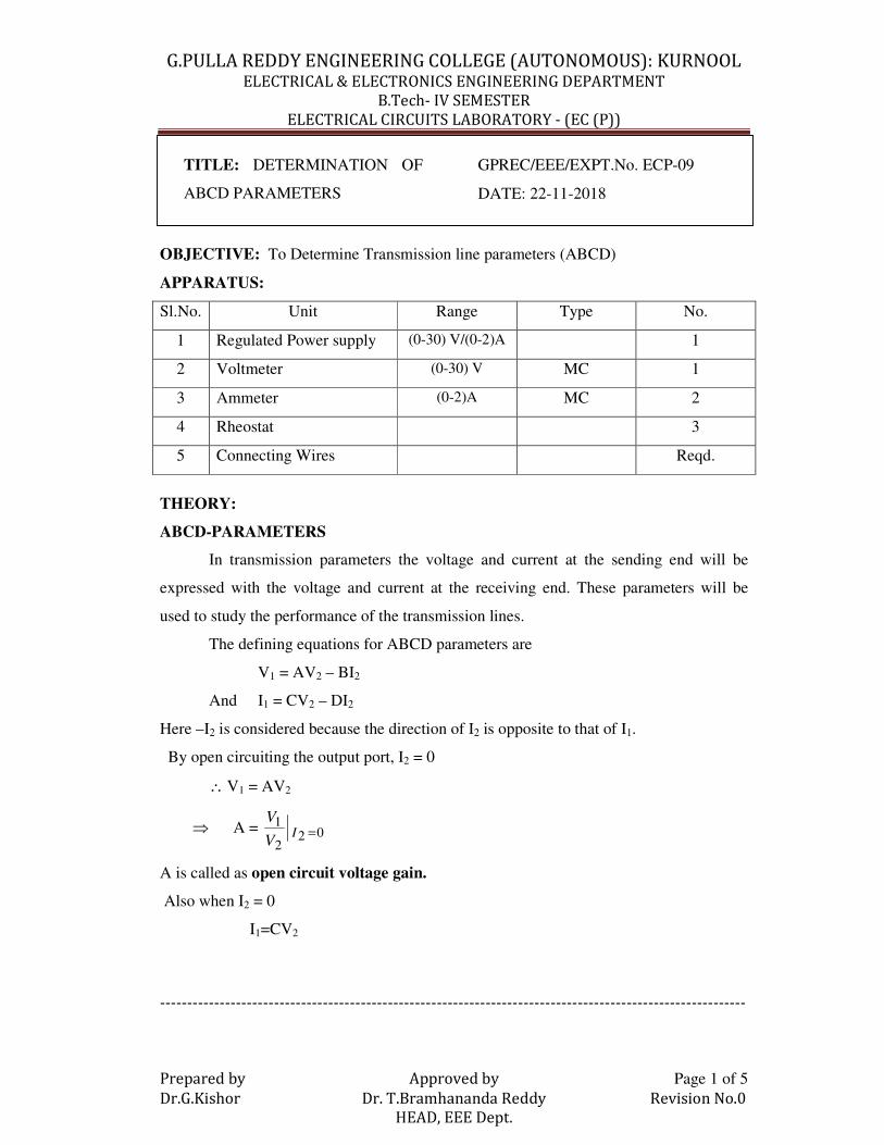
Step (i): By open circuiting the out put port, I2 tends to zero and so A and C can be
calculated
A = 2
1
V
V , Called reverse voltage ratio
C = 2
1
V
I , Called reverse transfer admittance.
Step (ii): By short circuiting the out put port, V2 tends to zero and so B and D can be
calculated.
- B = 2
1
I
V Called reverse transfer impedance
- D = 2
1
I
I Called reverse current ratio
A and D parameter has no units, parameter C in mho and parameter B is ohm.
CIRCUIT DIAGRAM:
Fig.1 To find Parameter ‘A’ & ‘C’

G.PULLA REDDY ENGINEERING COLLEGE (AUTONOMOUS): KURNOOL ELECTRICAL & ELECTRONICS ENGINEERING DEPARTMENT
B.Tech- IV SEMESTER
ELECTRICAL CIRCUITS LABORATORY - (EC (P))
------------------------------------------------------------------------------------------------------------
Prepared by Approved by Page 4 of 5
Dr.G.Kishor Dr. T.Bramhananda Reddy Revision No.0
HEAD, EEE Dept.
TITLE: DETERMINATION OF
ABCD PARAMETERS
GPREC/EEE/EXPT.No. ECP-09
DATE: 22-11-2018
Fig.2 To find Parameter ‘B’ & ‘D’
PROCEDURE:
TO FIND A, C PARAMETERS:
1. Connections are made as per the circuit diagram shown in Fig.1.
2. By varying V1, the corresponding readings of V2 and I1 are noted down.
3. A and C parameters are calculated.
TO FIND B, D PARAMETERS:
1. Connections are made as per the circuit diagram shown in Fig.2.
2. By varying V1, the corresponding readings of I1 and I2 are noted down.
3. B and D parameters are calculated.
TABULAR COLUMN:
S.No V1 V2 I1 A C
Th. Pr. Th. Pr.
S.No V1 I1 I2 B D
Th. Pr. Th. Pr.

G.PULLA REDDY ENGINEERING COLLEGE (AUTONOMOUS): KURNOOL ELECTRICAL & ELECTRONICS ENGINEERING DEPARTMENT
B.Tech- IV SEMESTER
ELECTRICAL CIRCUITS LABORATORY - (EC (P))
------------------------------------------------------------------------------------------------------------
Prepared by Approved by Page 5 of 5
Dr.G.Kishor Dr. T.Bramhananda Reddy Revision No.0
HEAD, EEE Dept.
TITLE: DETERMINATION OF
ABCD PARAMETERS
GPREC/EEE/EXPT.No. ECP-09
DATE: 22-11-2018
RESULT: ABCD parameters are determined.
Questions:
1. What are the defining equations of ABCD parameters
2. What is the significance of the two port parameters?
3. What is the applications of ABCD parameters?
4. What is the condition for symmetrical network?
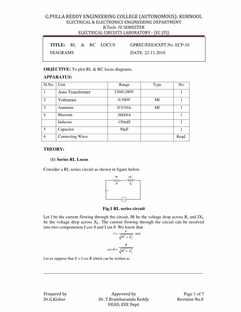
G.PULLA REDDY ENGINEERING COLLEGE (AUTONOMOUS): KURNOOL ELECTRICAL & ELECTRONICS ENGINEERING DEPARTMENT
B.Tech- IV SEMESTER
ELECTRICAL CIRCUITS LABORATORY - (EC (P))
------------------------------------------------------------------------------------------------------------
Prepared by Approved by Page 1 of 7
Dr.G.Kishor Dr. T.Bramhananda Reddy Revision No.0
HEAD, EEE Dept.
TITLE: RL & RC LOCUS
DIAGRAMS
GPREC/EEE/EXPT.No. ECP-10
DATE: 22-11-2018
OBJECTIVE: To plot RL & RC locus diagrams.
APPARATUS:
Sl.No. Unit Range Type No.
1 Auto Transformer 230/0-280V 1
2 Voltmeter 0-300V MI 1
3 Ammeter 0-5/10A MI 1
4 Rheostat 26Ω/4A 1
Inductor 150mH 1
5 Capacitor 50µF 1
6 Connecting Wires Reqd.
THEORY:
(1) Series RL Locus
Consider a RL series circuit as shown in figure below.
Fig.1 RL series circuit
Let I be the current flowing through the circuit, IR be the voltage drop across R, and IXL
be the voltage drop across XL. The current flowing through the circuit can be resolved
into two componenets I cos θ and I sin θ. We know that
Let us suppose that X = I cos θ which can be written as

G.PULLA REDDY ENGINEERING COLLEGE (AUTONOMOUS): KURNOOL ELECTRICAL & ELECTRONICS ENGINEERING DEPARTMENT
B.Tech- IV SEMESTER
ELECTRICAL CIRCUITS LABORATORY - (EC (P))
------------------------------------------------------------------------------------------------------------
Prepared by Approved by Page 2 of 7
Dr.G.Kishor Dr. T.Bramhananda Reddy Revision No.0
HEAD, EEE Dept.
TITLE: RL & RC LOCUS
DIAGRAMS
GPREC/EEE/EXPT.No. ECP-10
DATE: 22-11-2018
Similarly, let Y = I sin θ
Therefore, X
2 + Y
2 can be written as
And there fore
This can be modified as
The above expression represents a equation of a circle.
Locus diagram of R–L circuit when R is varying
Consider an R–L circuit in which R is varying from 0 to ∞.
The maximum current can be written as
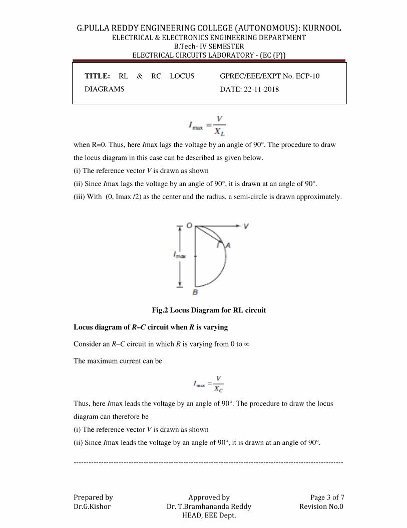
G.PULLA REDDY ENGINEERING COLLEGE (AUTONOMOUS): KURNOOL ELECTRICAL & ELECTRONICS ENGINEERING DEPARTMENT
B.Tech- IV SEMESTER
ELECTRICAL CIRCUITS LABORATORY - (EC (P))
------------------------------------------------------------------------------------------------------------
Prepared by Approved by Page 3 of 7
Dr.G.Kishor Dr. T.Bramhananda Reddy Revision No.0
HEAD, EEE Dept.
TITLE: RL & RC LOCUS
DIAGRAMS
GPREC/EEE/EXPT.No. ECP-10
DATE: 22-11-2018
when R=0. Thus, here Imax lags the voltage by an angle of 90°. The procedure to draw
the locus diagram in this case can be described as given below.
(i) The reference vector V is drawn as shown
(ii) Since Imax lags the voltage by an angle of 90°, it is drawn at an angle of 90°.
(iii) With (0, Imax /2) as the center and the radius, a semi-circle is drawn approximately.
Fig.2 Locus Diagram for RL circuit
Locus diagram of R–C circuit when R is varying
Consider an R–C circuit in which R is varying from 0 to ∞
The maximum current can be
Thus, here Imax leads the voltage by an angle of 90°. The procedure to draw the locus
diagram can therefore be
(i) The reference vector V is drawn as shown
(ii) Since Imax leads the voltage by an angle of 90°, it is drawn at an angle of 90°.
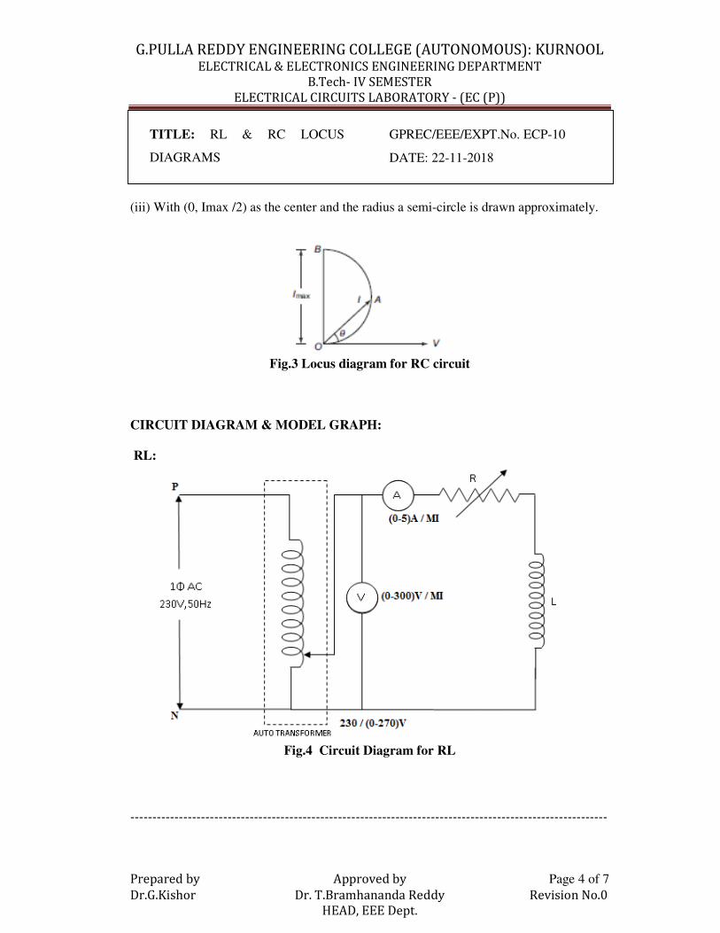
G.PULLA REDDY ENGINEERING COLLEGE (AUTONOMOUS): KURNOOL ELECTRICAL & ELECTRONICS ENGINEERING DEPARTMENT
B.Tech- IV SEMESTER
ELECTRICAL CIRCUITS LABORATORY - (EC (P))
------------------------------------------------------------------------------------------------------------
Prepared by Approved by Page 4 of 7
Dr.G.Kishor Dr. T.Bramhananda Reddy Revision No.0
HEAD, EEE Dept.
TITLE: RL & RC LOCUS
DIAGRAMS
GPREC/EEE/EXPT.No. ECP-10
DATE: 22-11-2018
(iii) With (0, Imax /2) as the center and the radius a semi-circle is drawn approximately.
Fig.3 Locus diagram for RC circuit
CIRCUIT DIAGRAM & MODEL GRAPH:
RL:
Fig.4 Circuit Diagram for RL

G.PULLA REDDY ENGINEERING COLLEGE (AUTONOMOUS): KURNOOL ELECTRICAL & ELECTRONICS ENGINEERING DEPARTMENT
B.Tech- IV SEMESTER
ELECTRICAL CIRCUITS LABORATORY - (EC (P))
------------------------------------------------------------------------------------------------------------
Prepared by Approved by Page 5 of 7
Dr.G.Kishor Dr. T.Bramhananda Reddy Revision No.0
HEAD, EEE Dept.
TITLE: RL & RC LOCUS
DIAGRAMS
GPREC/EEE/EXPT.No. ECP-10
DATE: 22-11-2018
Fig.5 Locus Diagram for RL circuit
RC:
Fig.6 Circuit Diagram for RC
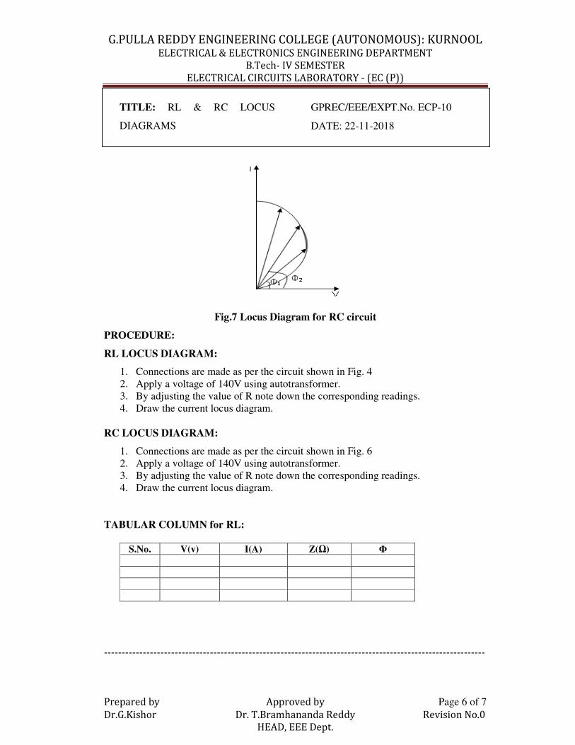
G.PULLA REDDY ENGINEERING COLLEGE (AUTONOMOUS): KURNOOL ELECTRICAL & ELECTRONICS ENGINEERING DEPARTMENT
B.Tech- IV SEMESTER
ELECTRICAL CIRCUITS LABORATORY - (EC (P))
------------------------------------------------------------------------------------------------------------
Prepared by Approved by Page 6 of 7
Dr.G.Kishor Dr. T.Bramhananda Reddy Revision No.0
HEAD, EEE Dept.
TITLE: RL & RC LOCUS
DIAGRAMS
GPREC/EEE/EXPT.No. ECP-10
DATE: 22-11-2018
Fig.7 Locus Diagram for RC circuit
PROCEDURE:
RL LOCUS DIAGRAM:
1. Connections are made as per the circuit shown in Fig. 4
2. Apply a voltage of 140V using autotransformer.
3. By adjusting the value of R note down the corresponding readings.
4. Draw the current locus diagram.
RC LOCUS DIAGRAM:
1. Connections are made as per the circuit shown in Fig. 6
2. Apply a voltage of 140V using autotransformer.
3. By adjusting the value of R note down the corresponding readings.
4. Draw the current locus diagram.
TABULAR COLUMN for RL:
S.No. V(v) I(A) Z(Ω) Φ
G.PULLA REDDY ENGINEERING COLLEGE (AUTONOMOUS): KURNOOL ELECTRICAL & ELECTRONICS ENGINEERING DEPARTMENT
B.Tech- IV SEMESTER
ELECTRICAL CIRCUITS LABORATORY - (EC (P))
------------------------------------------------------------------------------------------------------------
Prepared by Approved by Page 7 of 7
Dr.G.Kishor Dr. T.Bramhananda Reddy Revision No.0
HEAD, EEE Dept.
TITLE: RL & RC LOCUS
DIAGRAMS
GPREC/EEE/EXPT.No. ECP-10
DATE: 22-11-2018
TABULAR COLUMN for RC:
S.No. V(v) I(A) Z(Ω) Φ
RESULT: RL and RC locus diagrams are drawn.
Questions:
1. Differentiate RL and RC locus diagrams.
2. What is the power factor in RL and RC series circuits?
3. Write the equation for impedance in RL and RC series circuits.
4. How the loci could differ from RL and RC parallel circuits from RL and RC
series circuits.
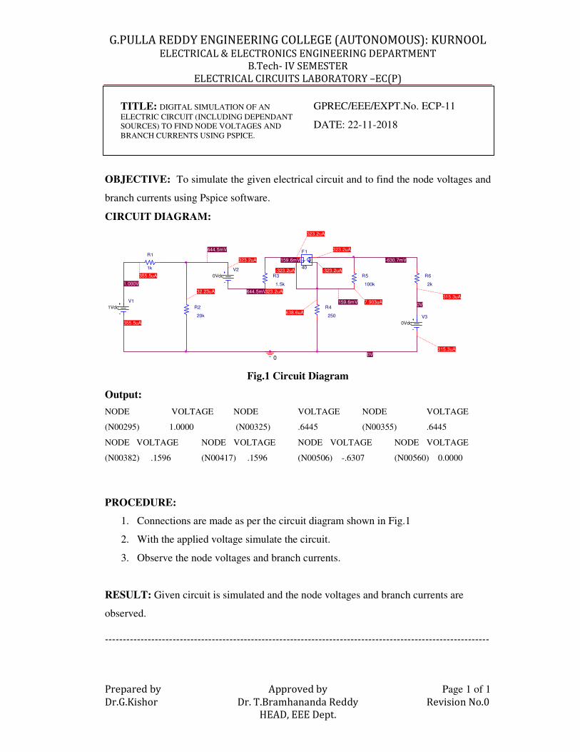
G.PULLA REDDY ENGINEERING COLLEGE (AUTONOMOUS): KURNOOL ELECTRICAL & ELECTRONICS ENGINEERING DEPARTMENT
B.Tech- IV SEMESTER
ELECTRICAL CIRCUITS LABORATORY –EC(P)
------------------------------------------------------------------------------------------------------------
Prepared by Approved by Page 1 of 1
Dr.G.Kishor Dr. T.Bramhananda Reddy Revision No.0
HEAD, EEE Dept.
TITLE: DIGITAL SIMULATION OF AN
ELECTRIC CIRCUIT (INCLUDING DEPENDANT
SOURCES) TO FIND NODE VOLTAGES AND
BRANCH CURRENTS USING PSPICE.
GPREC/EEE/EXPT.No. ECP-11
DATE: 22-11-2018
OBJECTIVE: To simulate the given electrical circuit and to find the node voltages and
branch currents using Pspice software.
CIRCUIT DIAGRAM:
159.6mV
F1
40
323.2uA
-323.2uA
323.2uA
-323.2uA
644.5mV
R4
250638.6uA
1.000V
R1
1k
355.5uA
0
R6
2k
315.3uA
R2
20k
32.23uA
644.5mV
V1
1Vdc
355.5uA
0V
R3
1.5k
323.2uA
V3
0Vdc
315.3uA
0V
-630.7mV
R5
100k
7.903uA159.6mV
V2
0Vdc
323.2uA
Fig.1 Circuit Diagram
Output:
NODE VOLTAGE NODE VOLTAGE NODE VOLTAGE
(N00295) 1.0000 (N00325) .6445 (N00355) .6445
NODE VOLTAGE NODE VOLTAGE NODE VOLTAGE NODE VOLTAGE
(N00382) .1596 (N00417) .1596 (N00506) -.6307 (N00560) 0.0000
PROCEDURE:
1. Connections are made as per the circuit diagram shown in Fig.1
2. With the applied voltage simulate the circuit.
3. Observe the node voltages and branch currents.
RESULT: Given circuit is simulated and the node voltages and branch currents are
observed.
G.PULLA REDDY ENGINEERING COLLEGE (AUTONOMOUS): KURNOOL ELECTRICAL & ELECTRONICS ENGINEERING DEPARTMENT
B.Tech- IV SEMESTER
ELECTRICAL CIRCUITS LABORATORY –EC(P)
------------------------------------------------------------------------------------------------------------
Prepared by Approved by Page 2 of 2
Dr.G.Kishor Dr. T.Bramhananda Reddy Revision No.0
HEAD, EEE Dept.
TITLE: DIGITAL SIMULATION OF AN
ELECTRIC CIRCUIT (INCLUDING DEPENDANT
SOURCES) TO FIND NODE VOLTAGES AND
BRANCH CURRENTS USING PSPICE.
GPREC/EEE/EXPT.No. ECP-11
DATE: 22-11-2018
Questions:
1. Define node.
2. Explain the procedure to find branch currents using current division.
3. Give the difference between ideal and dependent sources?
4. Give the syntax for dependent sources using Pspice?
5. Why the dummy voltage is mentioned with 0V and what is the purpose of it?
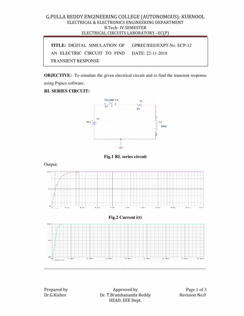
G.PULLA REDDY ENGINEERING COLLEGE (AUTONOMOUS): KURNOOL ELECTRICAL & ELECTRONICS ENGINEERING DEPARTMENT
B.Tech- IV SEMESTER
ELECTRICAL CIRCUITS LABORATORY –EC(P)
------------------------------------------------------------------------------------------------------------
Prepared by Approved by Page 1 of 3
Dr.G.Kishor Dr. T.Bramhananda Reddy Revision No.0
HEAD, EEE Dept.
TITLE: DIGITAL SIMULATION OF
AN ELECTRIC CIRCUIT TO FIND
TRANSIENT RESPONSE
GPREC/EEE/EXPT.No. ECP-12
DATE: 22-11-2018
OBJECTIVE: To simulate the given electrical circuit and to find the transient response
using Pspice software.
RL SERIES CIRCUIT:
Fig.1 RL series circuit
Output:
Fig.2 Current i(t)

G.PULLA REDDY ENGINEERING COLLEGE (AUTONOMOUS): KURNOOL ELECTRICAL & ELECTRONICS ENGINEERING DEPARTMENT
B.Tech- IV SEMESTER
ELECTRICAL CIRCUITS LABORATORY –EC(P)
------------------------------------------------------------------------------------------------------------
Prepared by Approved by Page 2 of 3
Dr.G.Kishor Dr. T.Bramhananda Reddy Revision No.0
HEAD, EEE Dept.
TITLE: DIGITAL SIMULATION OF
AN ELECTRIC CIRCUIT TO FIND
TRANSIENT RESPONSE
GPREC/EEE/EXPT.No. ECP-12
DATE: 22-11-2018
Fig.3 Voltage across resistor
RC SERIES CIRCUIT:
Fig.4 RC series circuit
Output:
Fig.5 Current i(t)
Fig.6 Voltage across resistor
PROCEDURE:
1. Connections are made as per the circuit diagram shown in Fig.1 and Fig.4
2. With the applied voltage simulate the circuit.
G.PULLA REDDY ENGINEERING COLLEGE (AUTONOMOUS): KURNOOL ELECTRICAL & ELECTRONICS ENGINEERING DEPARTMENT
B.Tech- IV SEMESTER
ELECTRICAL CIRCUITS LABORATORY –EC(P)
------------------------------------------------------------------------------------------------------------
Prepared by Approved by Page 3 of 3
Dr.G.Kishor Dr. T.Bramhananda Reddy Revision No.0
HEAD, EEE Dept.
TITLE: DIGITAL SIMULATION OF
AN ELECTRIC CIRCUIT TO FIND
TRANSIENT RESPONSE
GPREC/EEE/EXPT.No. ECP-12
DATE: 22-11-2018
3. Observe the current waveform and voltage across the resistor.
RESULT: RL and RC circuits are simulated and the transient response is observed.
Questions:
1. Define time constant of RL Circuit.
2. Define time constant of RC Circuit.
3. What is the time taken for the current to reach its steady state value in RL charging
circuit?
4. What is the time taken for the voltage to reach its steady state value in RC charging
circuit?
5. What is the voltage across the capacitor after 10τ sec in an RC discharging circuit?
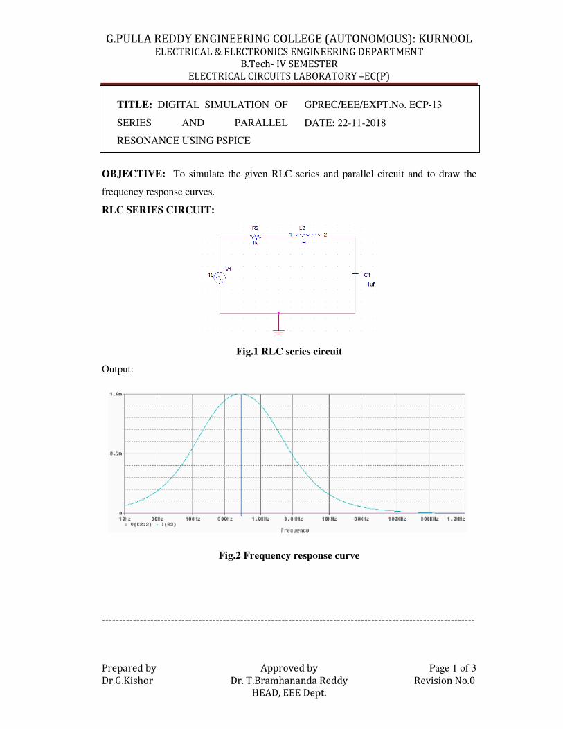
G.PULLA REDDY ENGINEERING COLLEGE (AUTONOMOUS): KURNOOL ELECTRICAL & ELECTRONICS ENGINEERING DEPARTMENT
B.Tech- IV SEMESTER
ELECTRICAL CIRCUITS LABORATORY –EC(P)
------------------------------------------------------------------------------------------------------------
Prepared by Approved by Page 1 of 3
Dr.G.Kishor Dr. T.Bramhananda Reddy Revision No.0
HEAD, EEE Dept.
TITLE: DIGITAL SIMULATION OF
SERIES AND PARALLEL
RESONANCE USING PSPICE
GPREC/EEE/EXPT.No. ECP-13
DATE: 22-11-2018
OBJECTIVE: To simulate the given RLC series and parallel circuit and to draw the
frequency response curves.
RLC SERIES CIRCUIT:
Fig.1 RLC series circuit
Output:
Fig.2 Frequency response curve
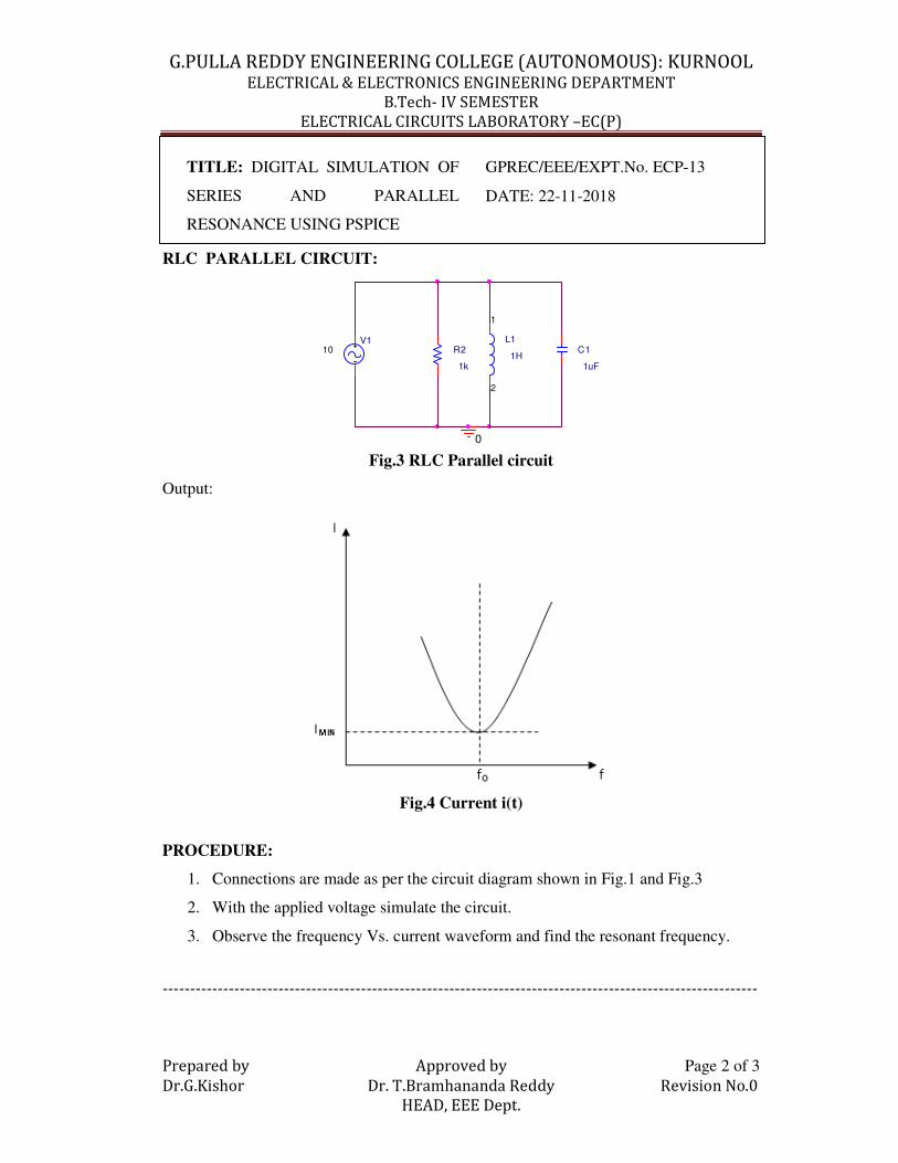
G.PULLA REDDY ENGINEERING COLLEGE (AUTONOMOUS): KURNOOL ELECTRICAL & ELECTRONICS ENGINEERING DEPARTMENT
B.Tech- IV SEMESTER
ELECTRICAL CIRCUITS LABORATORY –EC(P)
------------------------------------------------------------------------------------------------------------
Prepared by Approved by Page 2 of 3
Dr.G.Kishor Dr. T.Bramhananda Reddy Revision No.0
HEAD, EEE Dept.
TITLE: DIGITAL SIMULATION OF
SERIES AND PARALLEL
RESONANCE USING PSPICE
GPREC/EEE/EXPT.No. ECP-13
DATE: 22-11-2018
RLC PARALLEL CIRCUIT:
C1
1uF
V1
10 R2
1k
0
L1
1H
1
2
Fig.3 RLC Parallel circuit
Output:
Fig.4 Current i(t)
PROCEDURE:
1. Connections are made as per the circuit diagram shown in Fig.1 and Fig.3
2. With the applied voltage simulate the circuit.
3. Observe the frequency Vs. current waveform and find the resonant frequency.
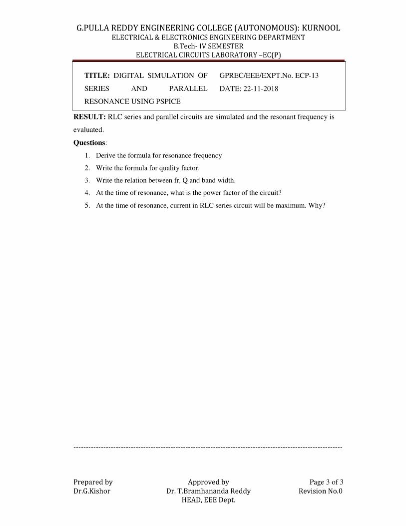
G.PULLA REDDY ENGINEERING COLLEGE (AUTONOMOUS): KURNOOL ELECTRICAL & ELECTRONICS ENGINEERING DEPARTMENT
B.Tech- IV SEMESTER
ELECTRICAL CIRCUITS LABORATORY –EC(P)
------------------------------------------------------------------------------------------------------------
Prepared by Approved by Page 3 of 3
Dr.G.Kishor Dr. T.Bramhananda Reddy Revision No.0
HEAD, EEE Dept.
TITLE: DIGITAL SIMULATION OF
SERIES AND PARALLEL
RESONANCE USING PSPICE
GPREC/EEE/EXPT.No. ECP-13
DATE: 22-11-2018
RESULT: RLC series and parallel circuits are simulated and the resonant frequency is
evaluated.
Questions:
1. Derive the formula for resonance frequency
2. Write the formula for quality factor.
3. Write the relation between fr, Q and band width.
4. At the time of resonance, what is the power factor of the circuit?
5. At the time of resonance, current in RLC series circuit will be maximum. Why?
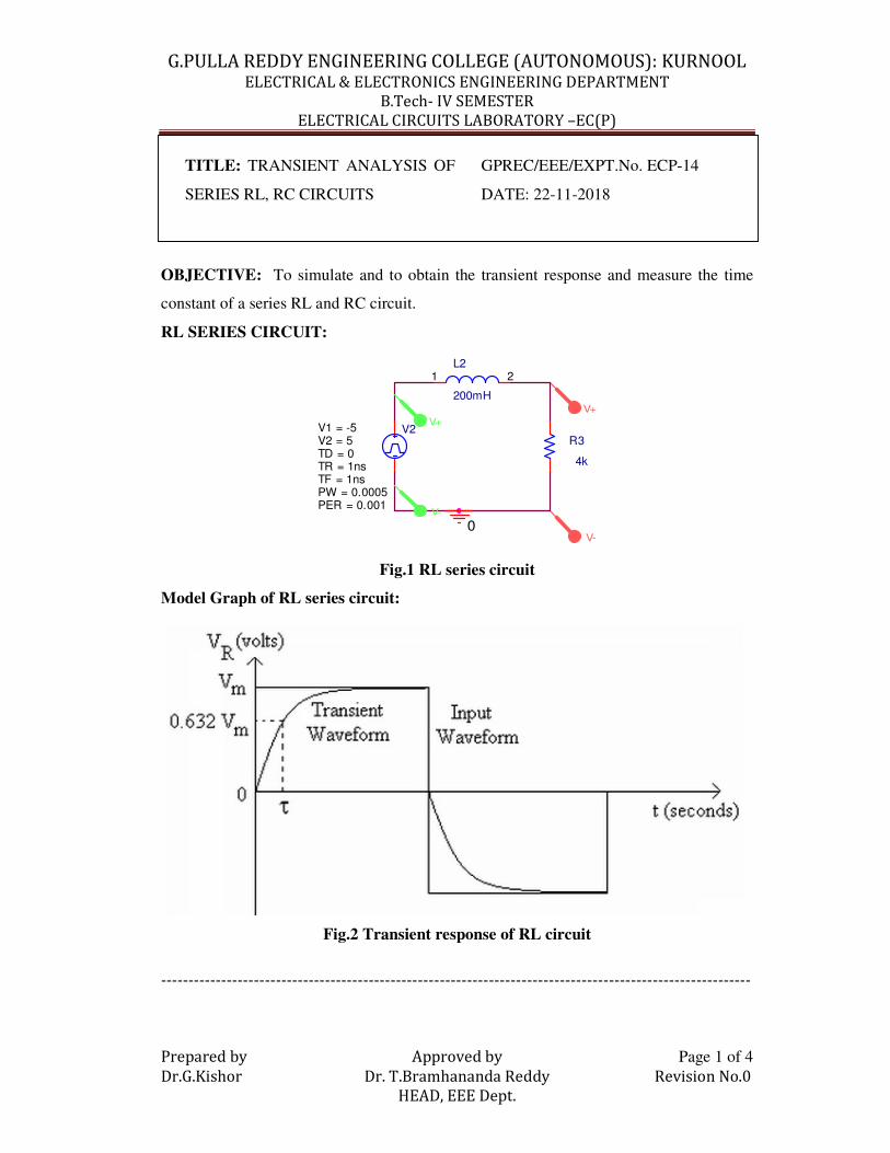
G.PULLA REDDY ENGINEERING COLLEGE (AUTONOMOUS): KURNOOL ELECTRICAL & ELECTRONICS ENGINEERING DEPARTMENT
B.Tech- IV SEMESTER
ELECTRICAL CIRCUITS LABORATORY –EC(P)
------------------------------------------------------------------------------------------------------------
Prepared by Approved by Page 1 of 4
Dr.G.Kishor Dr. T.Bramhananda Reddy Revision No.0
HEAD, EEE Dept.
TITLE: TRANSIENT ANALYSIS OF
SERIES RL, RC CIRCUITS
GPREC/EEE/EXPT.No. ECP-14
DATE: 22-11-2018
OBJECTIVE: To simulate and to obtain the transient response and measure the time
constant of a series RL and RC circuit.
RL SERIES CIRCUIT:
V-
R3
4k
V2
TD = 0
TF = 1ns
PW = 0.0005
PER = 0.001
V1 = -5
TR = 1ns
V2 = 5
L2
200mH
1 2
V+
V+
0
V-
Fig.1 RL series circuit
Model Graph of RL series circuit:
Fig.2 Transient response of RL circuit
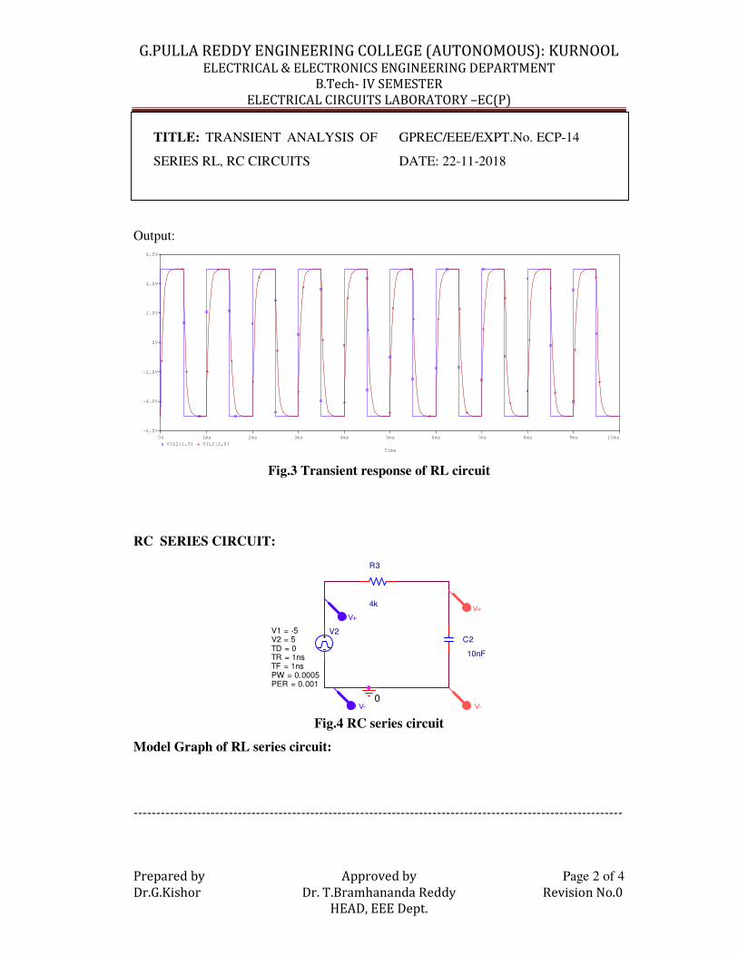
G.PULLA REDDY ENGINEERING COLLEGE (AUTONOMOUS): KURNOOL ELECTRICAL & ELECTRONICS ENGINEERING DEPARTMENT
B.Tech- IV SEMESTER
ELECTRICAL CIRCUITS LABORATORY –EC(P)
------------------------------------------------------------------------------------------------------------
Prepared by Approved by Page 2 of 4
Dr.G.Kishor Dr. T.Bramhananda Reddy Revision No.0
HEAD, EEE Dept.
TITLE: TRANSIENT ANALYSIS OF
SERIES RL, RC CIRCUITS
GPREC/EEE/EXPT.No. ECP-14
DATE: 22-11-2018
Output:
Time
0s 1ms 2ms 3ms 4ms 5ms 6ms 7ms 8ms 9ms 10ms
V(L2:1,0) V(L2:2,0)
-6.0V
-4.0V
-2.0V
0V
2.0V
4.0V
6.0V
Fig.3 Transient response of RL circuit
RC SERIES CIRCUIT:
V-
V2
TD = 0
TF = 1ns
PW = 0.0005
PER = 0.001
V1 = -5
TR = 1ns
V2 = 5
V+
R3
4k
0
V+
C2
10nF
V- Fig.4 RC series circuit
Model Graph of RL series circuit:
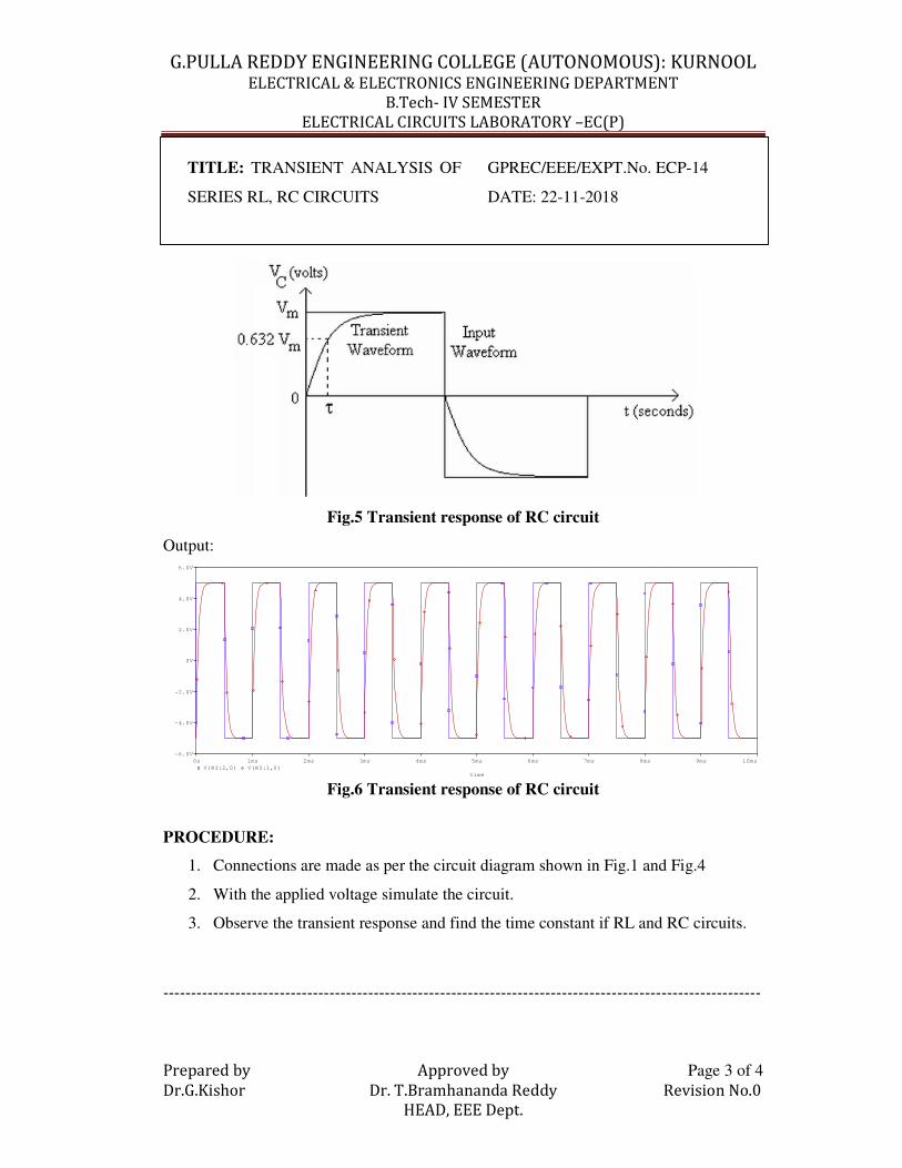
G.PULLA REDDY ENGINEERING COLLEGE (AUTONOMOUS): KURNOOL ELECTRICAL & ELECTRONICS ENGINEERING DEPARTMENT
B.Tech- IV SEMESTER
ELECTRICAL CIRCUITS LABORATORY –EC(P)
------------------------------------------------------------------------------------------------------------
Prepared by Approved by Page 3 of 4
Dr.G.Kishor Dr. T.Bramhananda Reddy Revision No.0
HEAD, EEE Dept.
TITLE: TRANSIENT ANALYSIS OF
SERIES RL, RC CIRCUITS
GPREC/EEE/EXPT.No. ECP-14
DATE: 22-11-2018
Fig.5 Transient response of RC circuit
Output:
Time
0s 1ms 2ms 3ms 4ms 5ms 6ms 7ms 8ms 9ms 10ms
V(R3:2,0) V(R3:1,0)
-6.0V
-4.0V
-2.0V
0V
2.0V
4.0V
6.0V
Fig.6 Transient response of RC circuit
PROCEDURE:
1. Connections are made as per the circuit diagram shown in Fig.1 and Fig.4
2. With the applied voltage simulate the circuit.
3. Observe the transient response and find the time constant if RL and RC circuits.
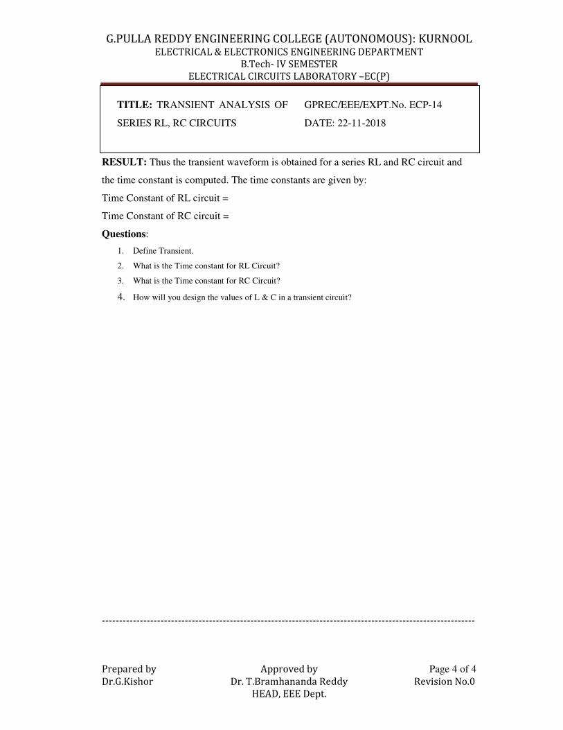
G.PULLA REDDY ENGINEERING COLLEGE (AUTONOMOUS): KURNOOL ELECTRICAL & ELECTRONICS ENGINEERING DEPARTMENT
B.Tech- IV SEMESTER
ELECTRICAL CIRCUITS LABORATORY –EC(P)
------------------------------------------------------------------------------------------------------------
Prepared by Approved by Page 4 of 4
Dr.G.Kishor Dr. T.Bramhananda Reddy Revision No.0
HEAD, EEE Dept.
TITLE: TRANSIENT ANALYSIS OF
SERIES RL, RC CIRCUITS
GPREC/EEE/EXPT.No. ECP-14
DATE: 22-11-2018
RESULT: Thus the transient waveform is obtained for a series RL and RC circuit and
the time constant is computed. The time constants are given by:
Time Constant of RL circuit =
Time Constant of RC circuit =
Questions:
1. Define Transient.
2. What is the Time constant for RL Circuit?
3. What is the Time constant for RC Circuit?
4. How will you design the values of L & C in a transient circuit?

G.PULLA REDDY ENGINEERING COLLEGE (AUTONOMOUS): KURNOOL ELECTRICAL & ELECTRONICS ENGINEERING DEPARTMENT
B.Tech- IV SEMESTER
ELECTRICAL CIRCUITS LABORATORY –EC(P)
------------------------------------------------------------------------------------------------------------
Prepared by Approved by Page 1 of 4
Dr.G.Kishor Dr. T.Bramhananda Reddy Revision No.0
HEAD, EEE Dept.
TITLE: FREQUENCY RESPONSE
OF SINGLE TUNED COUPLED
CIRCUIT
GPREC/EEE/EXPT.No. ECP-15
DATE: 22-11-2018
OBJECTIVE: To Plot the Frequency Response of a single stage RC Coupled Amplifier
with feedback and without feedback and find the following:
1. Voltage Gain
2. Lower cut off Frequency
3. Upper cut off Frequency
4. Bandwidth
5. Gain Bandwidth Product
Apparatus:
1. Transistor – BC 107
2. Resistors – 1K,10K,100K.
3. Capacitors – 10nF, 1uF(2No’s).
4. Inductor – 40 mH.
Software Tool: TinaPro
Introduction
A practical amplifier circuit is meant to raise the voltage level of the input signal.
This signal may be obtained from anywhere e.g. radio or TV receiver circuit. Such a
signal is not of a single frequency. But it consists of a band of frequencies, e.g. from 20
Hz to 20 KHz. If the loudspeakers are to reproduce the sound faithfully, the
amplifier used must amplify all the frequency components of signal by same
amount. If it does not do so, the output of the loudspeaker will not be the exact replica
of the original sound. When this happen then it means distortion has been introduced by
the amplifier. Consider an RC coupled amplifier circuit shown fig.1 shows frequency
response curve of a RC coupled amplifier. The curve is usually plotted on a semi log
graph paper with frequency range on logarithmic scale so that large frequency range can
be accommodated. The gain is constant for a limited band of frequencies. This

G.PULLA REDDY ENGINEERING COLLEGE (AUTONOMOUS): KURNOOL ELECTRICAL & ELECTRONICS ENGINEERING DEPARTMENT
B.Tech- IV SEMESTER
ELECTRICAL CIRCUITS LABORATORY –EC(P)
------------------------------------------------------------------------------------------------------------
Prepared by Approved by Page 2 of 4
Dr.G.Kishor Dr. T.Bramhananda Reddy Revision No.0
HEAD, EEE Dept.
TITLE: FREQUENCY RESPONSE
OF SINGLE TUNED COUPLED
CIRCUIT
GPREC/EEE/EXPT.No. ECP-15
DATE: 22-11-2018
BC107
100k
10k
1k 1
u 1
0n
1u
40m
+
Vcc=12V
+
Vin=20mV
Vo
range is called mid-frequency band and gain is called mid band gain. AVM. On
both sides of the mid frequency range, the gain decreases. For very low and very
high frequencies the gain is almost zero.
In mid band frequency range, the coupling capacitors and bypass capacitors are as
good as short circuits. But when the frequency is low. These capacitors can no longer be
replaced by the short circuit approximation.
At low frequency, output capacitor reactance increases. The voltage across
RL Reduces because some voltage drop takes place across XC. Thus output voltage
reduces.
The XC reactance not only reduces the gain but also change the phase between
input and output. It would not be exactly 180o but decided by the reactance. At zero
frequency, the capacitors are open circuited therefore output voltage reduces to zero.
CIRCUIT DIAGRAM:

G.PULLA REDDY ENGINEERING COLLEGE (AUTONOMOUS): KURNOOL ELECTRICAL & ELECTRONICS ENGINEERING DEPARTMENT
B.Tech- IV SEMESTER
ELECTRICAL CIRCUITS LABORATORY –EC(P)
------------------------------------------------------------------------------------------------------------
Prepared by Approved by Page 3 of 4
Dr.G.Kishor Dr. T.Bramhananda Reddy Revision No.0
HEAD, EEE Dept.
TITLE: FREQUENCY RESPONSE
OF SINGLE TUNED COUPLED
CIRCUIT
GPREC/EEE/EXPT.No. ECP-15
DATE: 22-11-2018
PROCEDURE:
1. Open TinaPro Software to design single Tuned amplifier circuit
2. Select on New editor window and place the required component on the circuit window.
3. Make the connections using wire and check the connections.
4. Go for simulation and using Run Key observe the output waveforms on CRO
5. Observe the Ac Analysis and draw the magnitude response curve
6. Calculate the bandwidth and Quality factor of the amplifier
FREQUENCY RESPONSE:
------------------
Gain in dB --------------------------
f1 f0 f2 Frequency
CALCULATIONS:

G.PULLA REDDY ENGINEERING COLLEGE (AUTONOMOUS): KURNOOL ELECTRICAL & ELECTRONICS ENGINEERING DEPARTMENT
B.Tech- IV SEMESTER
ELECTRICAL CIRCUITS LABORATORY –EC(P)
------------------------------------------------------------------------------------------------------------
Prepared by Approved by Page 4 of 4
Dr.G.Kishor Dr. T.Bramhananda Reddy Revision No.0
HEAD, EEE Dept.
TITLE: FREQUENCY RESPONSE
OF SINGLE TUNED COUPLED
CIRCUIT
GPREC/EEE/EXPT.No. ECP-15
DATE: 22-11-2018
Table:
RESULT:
Questions:
1. What is a tuned amplifier
2. Define Q-factor
3. What is selectivity?
4. Is tuned amplifier a hallow band or wide band amplifier
5. Give the applications for tuned amplifier
SL
No
Input ac voltage(Vi) : Volts
Frequency
(Hz)
Output voltage
Volts (Vo)
Voltage gain
Av = Vo/Vi
Gain in dB
20 log Av
Quality Factor
Theoretical
Practical


![INDEX [studentsfocus.com]studentsfocus.com/notes/anna_university/IT/4SEM... · cs6412 – microprocessor and microcontroller lab dept of cse 2 expt.no name of the experiment page](https://img.pdfslide.us/doc/110x75/5afd184c7f8b9a323491255e/index-microprocessor-and-microcontroller-lab-dept-of-cse-2-exptno-name.jpg)