Embed Size (px)
Citation preview

Kirchhoff’s Voltage and Current Laws (KVL and KCL)- Sum of voltages around a closed loop equals zero (KVL)
- Sum of currents entering any node equals zero (KCL)
V = iR (Ohm's Law)
-V + V + V = 0 (KVL)
V + V = 5V
V = I R ; V = IR (KCL)
S 1 2
1 2
1 1 2 2

V = V = 10V (KVL)
I = V
R =
10V
5 = 2A ; I =
10V
20 = 0.5A (Ohm' s Law)
I + I + I = 0 (KCL)
-2A - 0.5A + I = 0
I = 2.5A
1 2
11
12
1 2 3
3
3
Ω Ω
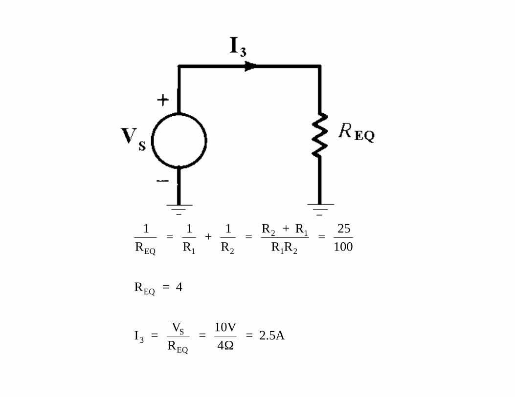
1
R =
1
R +
1
R =
R + R
R R =
25
100
R = 4
I = V
R =
10V
4 = 2.5A
EQ 1 2
2 1
1 2
EQ
3S
EQ Ω
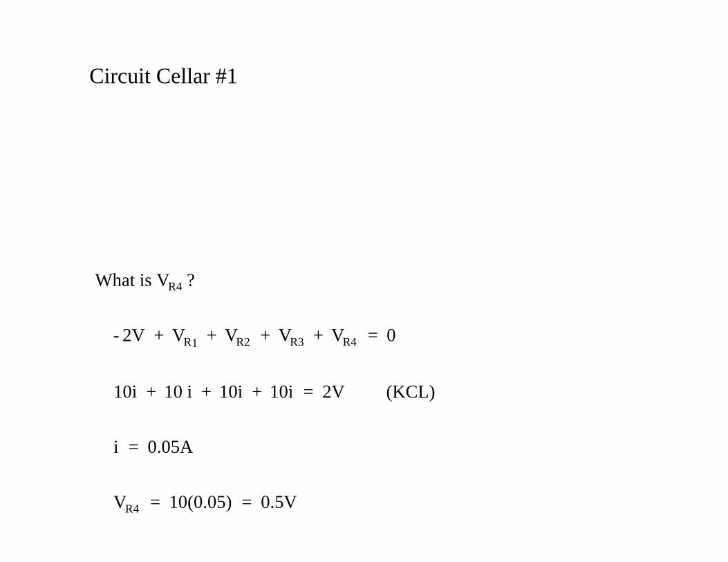
Circuit Cellar #1
What is V
- 2V + V + V + V + V = 0
10i + 10 i + 10i + 10i = 2V (KCL)
i = 0.05A
V = 10(0.05) = 0.5V
R4
R1 R2 R3 R4
R4
?

Voltage/Current Characteristics - very important concept in electronics
- measure voltage and current through terminals (ports)
- concise description of device operation
- graphical representation
- can be extended to more general concept
- complex devices
- multiple devices
- Resistor
i = V/R (Ohm’s Law); di/dv = 1/R (slope)--------->linear device
Figure 1.3Plot of v-icharacteristic of a10kΩ resistor
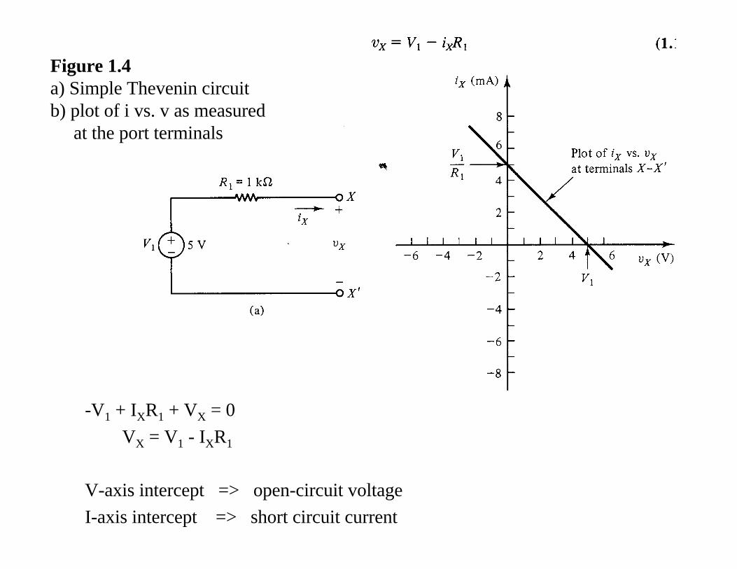
-V1 + IXR1 + VX = 0
VX = V1 - IXR1
V-axis intercept => open-circuit voltage
I-axis intercept => short circuit current
Figure 1.4 a) Simple Thevenin circuitb) plot of i vs. v as measured at the port terminals

Non-linear Device ==> Diode
- non-linearity (not a straight line)
- direction of flow same as symbol arrow
- negative voltage => current is approx. 0 (10-10 A) (reverse biased)
- positive voltage threshold (turn-on voltage) => (Si = 0.6V; Ge = 0.2V)
- sufficient forward voltage => current?
- reverse bias breakdown
ID = IS(e VD/ηVT-1)
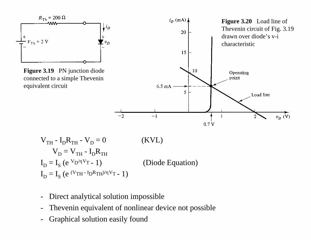
VTH - IDRTH - VD = 0 (KVL)
VD = VTH - IDRTH
ID = IS (e VD/ηVT - 1) (Diode Equation)
ID = IS (e (VTH - IDRTH)/ηVT - 1)
- Direct analytical solution impossible
- Thevenin equivalent of nonlinear device not possible
- Graphical solution easily found
Figure 3.19 PN junction diodeconnected to a simple Theveninequivalent circuit
Figure 3.20 Load line of Thevenin circuit of Fig. 3.19drawn over diode’s v-icharacteristic

- reverse polarity of diode
=> mirror of graph about x-axis and y-axis
Figure 3.21 Diode connected so that vD and iD are defined with opposite polarity to the terminal variables vX and iX of the Thevenin circuit

Semiconductor Materials
- silicon, germanium, gallium arsenide
- conductivity => number of charge carriers per unit volume
metal --- high conductivity
insulator --- low conductivity
semiconductor --- variable conductivity changed by the addition
of dopants
- crystalline structure (3-D)
- at T = 0 insulator
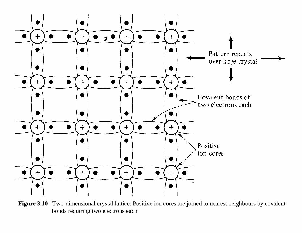
Figure 3.10 Two-dimensional crystal lattice. Positive ion cores are joined to nearest neighbours by covalent bonds requiring two electrons each

- as temperature rises, thermal vibration can break small number ofbonds
- generate hole-electron pairs
electron --- negative
hole --- positive
- holes and electrons can contribute to current
- equal number of holes and electrons called “intrinsic” semiconductor
Figure 3.11 Schematicrepresentation of athermally generatedhole-electron paircreated by the random breaking of a covalentbond
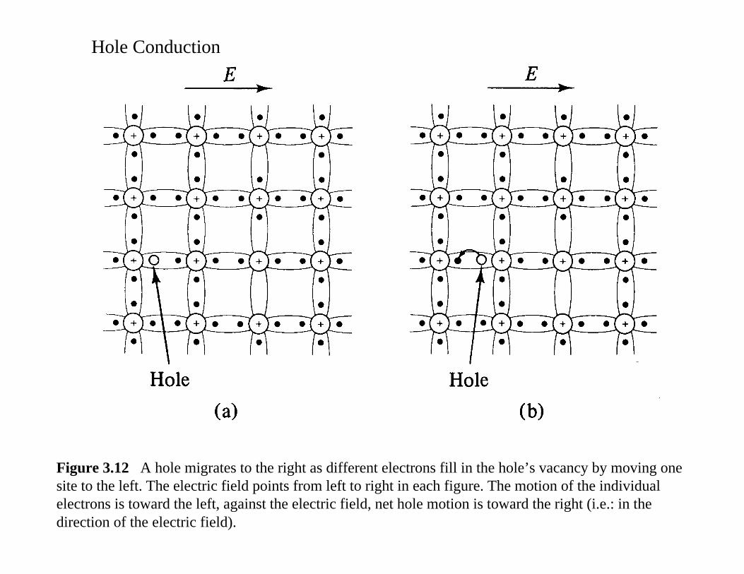
Hole Conduction
Figure 3.12 A hole migrates to the right as different electrons fill in the hole’s vacancy by moving onesite to the left. The electric field points from left to right in each figure. The motion of the individualelectrons is toward the left, against the electric field, net hole motion is toward the right (i.e.: in thedirection of the electric field).
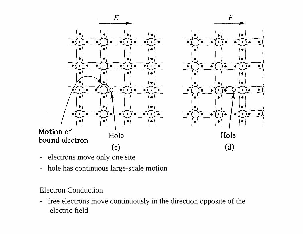
- electrons move only one site
- hole has continuous large-scale motion
Electron Conduction
- free electrons move continuously in the direction opposite of theelectric field

Donors and Acceptors- hole/electron concentrations can be changed by the additions of small
amounts of elements (dopants)
- added impurities create “extrinsic” semiconductorDopants acceptors - boron, indium, aluminum, donors - phosphorous, arsenic, antimony, (have extra electron)
Figure 3.13 A hole iscreated when a boundelectron falls into the empty covalent bondof an acceptor impurityA negatively charged, immobile acceptor ionis created in the process

Donors and Acceptors (con’t) - maintain charge neutrality
acceptors - mobile hole - p-type
donor - mobile electron - n-type
- minimum amount of energy to move unbound electrons/holes (i.e. easyto jump from one site to another)
Figure 3.14 A free electronis created as the outer electron of a donor atombreaks away from its bond.A positively charged, immobile donor ion is leftbehind
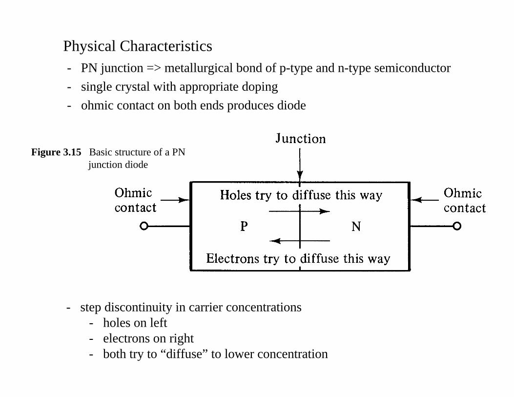
Physical Characteristics- PN junction => metallurgical bond of p-type and n-type semiconductor
- single crystal with appropriate doping
- ohmic contact on both ends produces diode
- step discontinuity in carrier concentrations - holes on left - electrons on right - both try to “diffuse” to lower concentration
Figure 3.15 Basic structure of a PN junction diode
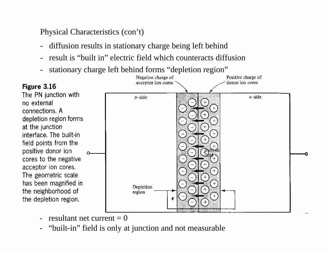
Physical Characteristics (con’t)
- diffusion results in stationary charge being left behind
- result is “built in” electric field which counteracts diffusion
- stationary charge left behind forms “depletion region”
- resultant net current = 0- “built-in” field is only at junction and not measurable

Forward Bias- apply positive voltage --- forward bias
- electric field diminishes “built-in” field- carriers no longer prevented from diffusing- as they cross over the barrier, holes and electrons become carriers and form “drift” current (carrier injection)

Forward Bias (con’t)
ID = IS(e VD/ηVT - 1)
- carrier injection causes exponential increase in current with appliedvoltage
IS => saturation current (approx. 10-12 A)
- donor and acceptor concentration
- temperature
- junction area
η => emission coefficient (recombination in depletion zone)
- type of diode Ge = 1
Si ~ 2
VT => thermal voltage (25mV @ T = 25oC) => (atoms bouncing)
= kT/q where k = Boltzman constant and
q = electrostatic charge
Reverse Bias
- electric field reinforces “built-in” field
- diffusion of carriers is suppressed
- no carrier injection
- ID = -IS (Ge is approx 1000X Si)
- reverse breakdown voltage
Circuit Cellar #2 Circuit Cellar #3
A) Is this a good circuit (yes or no)? What is the voltage VR1?
B) Why or why not? (IS = 10-12 A)

Zener Diode
- forward bias obeys exponential V-I characteristic
- if reverse bias becomes large, diode equation no longer obeyed
- at the zener voltage, VZk current can flow in the reverse direction
- heavily doped p-type and n-type regions produce large “built-in” field
Zener Diode (con’t)
- with reverse bias large “built-in” field is augmented by external voltage
- at VZk bound electrons are stripped away from atoms “zenerbreakdown”
- electrons can also be liberated when atoms are struck by other freeelectrons “avalanche breakdown”
- large number of carriers that can support current flow in the reversedirection
- sharp transition in diode curve
- if current is too large, catastrophic breakdown can result

Standard Diode
- will succumb to avalanche breakdown if reverse bias is great enough(small built-in field)
- typical breakdown ranges from 50-1000V and dependent uponfabrication parameters of junction
- reverse bias should not exceed “reverse breakdown voltage”
- if circuit limits current, reverse breakdown may not be fatal (i.e.: powerdissipation spec.)
- minimum guaranteed reverse breakdown voltage is called peak reverse
voltage (PRV)
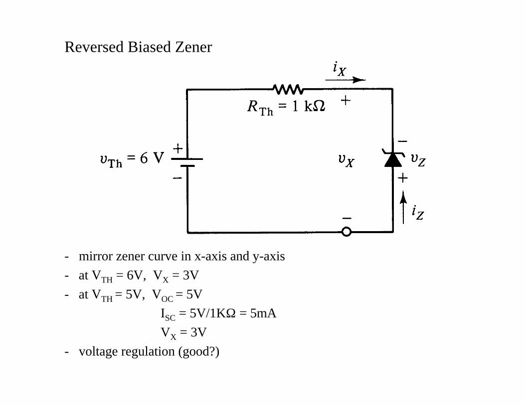
Reversed Biased Zener
- mirror zener curve in x-axis and y-axis
- at VTH = 6V, VX = 3V
- at VTH = 5V, VOC = 5V
ISC = 5V/1KΩ = 5mA
VX = 3V
- voltage regulation (good?)

Reversed Biased Zener
Figure 3.25 Load line of resistive circuitof previous slide superimposed on invertedv-i characteristic of the zener diode withVZK = 3V