Embed Size (px)
Citation preview
Laser-assisted direct ink writing of planar and 3Dmetal architecturesMark A. Skylar-Scotta,b, Suman Gunasekarana, and Jennifer A. Lewisa,b,1
aJohn A. Paulson School of Engineering and Applied Sciences, Harvard University, Cambridge, MA 02138; and bWyss Institute for Biologically InspiredEngineering, Harvard University, Cambridge, MA 02138
Edited by Yueh-Lin Loo, Princeton University, Princeton, NJ, and accepted by the Editorial Board April 4, 2016 (received for review December 19, 2015)
The ability to pattern planar and freestanding 3D metallic architec-tures at the microscale would enable myriad applications, includingflexible electronics, displays, sensors, and electrically small antennas.A 3D printing method is introduced that combines direct ink writ-ing with a focused laser that locally anneals printed metallic features“on-the-fly.” To optimize the nozzle-to-laser separation distance, theheat transfer along the printed silver wire is modeled as a function ofprinting speed, laser intensity, and pulse duration. Laser-assisted di-rect ink writing is used to pattern highly conductive, ductile metallicinterconnects, springs, and freestanding spiral architectures onflexible and rigid substrates.
3D printing | flexible electronics | conductive interconnects | silver ink |laser annealing
The ability to create planar and freestanding 3D metal structureson demand at the microscale would enable myriad applications,
including electronics (1–8), microelectromechanical systems (MEMS)(9, 10), metamaterials (11–13), and biomedical devices (14–16). Forexample, many electronic devices, such as inductors and antennas(4, 7), operate more efficiently in 3D form. However, that format isnot well suited to standard photolithographic techniques. A one-step process for directly writing conductive, ductile metal wiresand complex 3D architectures, such as freestanding spiral motifs,onto low-cost plastic and rigid substrates would enable high-performance, customizable electronic and other devices to bemanufactured in a cost-effective and space-efficient manner. Todate, several printing approaches have been developed to di-rectly deposit conductive features, including roll-to-roll (17–19),inkjet printing (20, 21), meniscus printing (8), and direct inkwriting (DIW) (1, 22). Although DIW has demonstrated spanninglinear traces or short arcs printed out-of-plane, only meniscus-basedelectrodeposition printing has been used to generate freestanding3D solid metal structures in arbitrary geometries. However, itsultralow print speed (<1 μm/s) coupled with the need for aconductive substrate have limited its widespread adoption (8).Here, we introduce laser-assisted direct ink writing (laser-DIW),
which combines printing of concentrated silver nanoparticle inkswithfocused infrared laser annealing to rapidly create high conductivity,ductilemetallic wires and 3D architectures “on-the-fly” in a one-step,additive process. Laser-DIW offers three key advantages over other3Dprinting techniques. First, by combining patterning and annealingin a single step, the printed metallic features exhibit the requisitemechanical properties needed to precisely fabricate arbitrary objectsin midair, enabling complex curvilinear structures to be generatedwithout the need for support material. Due to localized annealing,such features can be printed on low-cost plastic substrates, such aspoly(ethylene terphthalate) (PET). Finally, the patterned featuresexhibit high electrical conductivity approaching that of bulk silver.
Results and DiscussionDuring laser-DIW, an 808-nm IR laser is focused to a 100-μmspot adjacent to the aperture of the glass nozzle through which aconcentrated silver nanoparticle ink (85 wt % solids) is deposited(Fig. 1A and Fig. S1). Upon exiting the nozzle, the patterned fea-tures are rapidly heated by the focused laser to form a mechanically
robust, electrically conductive wire. The printed silver wires vary indiameter from <1 μm to 20 μm depending on the nozzle diameter,extrusion pressure, and printing speeds used. The in-line laserannealing process induces a visible change of emissivity (dull toshiny) of the printed wires at the macroscale (Fig. 1B), as well asthe densification of individual silver nanoparticles into largergrains at the microscale (Fig. 1C).To print curvilinear features via laser-DIW, the sample must be
rotated relative to the laser–nozzle axis using a rotary stage, suchthat the curvilinear wire is always patterned in a direction parallelto the laser–nozzle axis (Fig. 1 D and E, Fig. S2, and SupportingInformation). As the rotary stage moves, there exists a minimumradius of curvature of the metal trace ρmin such that the wirepasses through the laser spot, which depends upon the separationdistance l between the nozzle and the perimeter of the laser spotof diameter D (Fig. 1F and Fig. S3):
ρmin =lðl+DÞ
D. [1]
To create sharp turns, the laser must be placed as close to theink deposition nozzle as possible (Fig. 1G, Eq. 1). However,when the laser is positioned too close, heat is conducted up-stream through the silver ink and into the nozzle, resulting incessation of ink flow due to densification.To optimize the nozzle-to-laser separation distance, we use a
simplified one-dimensional heat transfer model to study the tem-perature distribution along the silver wire during printing at a speedvp, which accounts for the input laser energy ðqLÞ as well as con-vective ðqCÞ and radiative ðqRÞ heat loss. The temperature distri-bution is modeled by the following convection–diffusion equation:
∂T∂t
=∇ ·kðx, tÞ
ρðx, tÞcpðx, tÞ∇T − vp∇ ·T
+1
ρðx, tÞcpðx, tÞ ½qLðx, tÞ− qCðx, tÞ− qRðx, tÞ�, [2]
Significance
The growing demand for customized electronic devices underpinsthe need for 3D fabrication methods that enable form factorswell beyond those that are flat and rigid. A printing method isintroduced for one-step fabrication of conductive and ductile metalfeatures in planar and complex 3D shapes that combines direct inkwriting with “on-the-fly” laser annealing.
Author contributions: M.A.S.-S. and J.A.L. designed research; M.A.S.-S. and S.G. per-formed research; M.A.S.-S. analyzed data; and M.A.S.-S. and J.A.L. wrote the paper.
Conflict of interest statement: J.A.L. has cofounded a startup company, Voxel8 Inc, thatmay seek to license the intellectual property related to laser direct ink writing.
This article is a PNAS Direct Submission. Y.-L.L. is a guest editor invited by the Editorial Board.
Freely available online through the PNAS open access option.1To whom correspondence should be addressed. Email: [email protected].
This article contains supporting information online at www.pnas.org/lookup/suppl/doi:10.1073/pnas.1525131113/-/DCSupplemental.
www.pnas.org/cgi/doi/10.1073/pnas.1525131113 PNAS | May 31, 2016 | vol. 113 | no. 22 | 6137–6142
ENGINEE
RING
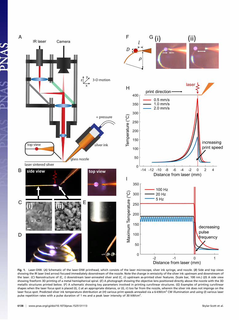
Fig. 1. Laser-DIW. (A) Schematic of the laser-DIW printhead, which consists of the laser microscope, silver ink syringe, and nozzle. (B) Side and top viewsshowing the IR laser (red arrow) focused immediately downstream of the nozzle. Note the change in emissivity of the silver ink upstream and downstream ofthe laser. (C) Nanostructure of (C, i) downstream laser-annealed silver and (C, ii) upstream as-printed silver features. (Scale bar, 100 nm.) (D) A side viewshowing freeform 3D printing of a metal hemispherical spiral. (E) A photograph showing the objective lens positioned directly above the nozzle with the 3Dmetallic structures printed below. (F) A schematic showing key parameters involved in printing curvilinear structures. (G) Examples of printing curvilinearshapes when the laser focus spot is placed (G, i) at an appropriate distance, or (G, ii) too far from the nozzle, wherein the silver ink does not impinge on thelaser focus spot. Predicted silver ink temperature distribution at (H) various print speeds annealed via a 6-kW/cm2 CW illumination and using (I) various laserpulse repetition rates with a pulse duration of 1 ms and a peak laser intensity of 30 kW/cm2.
6138 | www.pnas.org/cgi/doi/10.1073/pnas.1525131113 Skylar-Scott et al.
where the density ρ, the specific heat capacity cp, and the thermalconductivity k of printed wire are a function of its thermal his-tory. We numerically solve this partial differential equation usinga finite-difference method (Supporting Information). The up-stream heat transfer is reduced by three key mechanisms. First,using laser flash thermal analysis, we find that the heat-annealedsilver features have a 50-fold higher thermal diffusivity comparedwith the as-printed silver ink (20 mm2 s−1 and 0.4 mm2 s−1, re-spectively). Hence, the laser-annealed regions of the printed silverwires serve as a downstream heat sink, limiting upstream heattransfer to the ink reservoir within the nozzle. Second, the printingspeed limits upstream heat flow due to downstream heat advection,as shown by steady-state temperature curves generated by the sim-ulation during printing at various speeds under continuous-wave(CW) laser illumination (Fig. 1H). As an approximation, a charac-teristic upstream heating distance, Lc, is the length at which upstreamconductive heat flux is balanced by downstream heat advectionresulting from the printing velocity, i.e., the length for which thePéclet number is equal to unity:
Pe=Lcvpα
= 1. [3]
For example, using the thermal diffusivity for unannealed silverink (as-printed), the characteristic upstream heating distance at aprint speed of 1 mm s−1 is 400 μm. Notably, this printing speed ismore than 1,000× higher than meniscus printing. Finally, oper-ating the laser in a pulsed mode instead of CW allows one toachieve high maximum annealing temperatures while limiting thetotal heat transfer to the wire, with low pulse repetition rates (PRR)resulting in very limited upstream heat conduction (Fig. 1I). Toachieve a uniform densification through the thickness of theprinted wires, the laser pulse duration should be sufficiently longsuch that the characteristic thermal diffusion distance is largecompared with the wire diameter:
xc = 2ffiffiffiffi
αtp � dwire. [4]
For a pulse duration of 1 ms, this characteristic length is 40 μm,which is significantly larger than the thickest (∼20 μm) wiresbeing printed. The simulation further predicts that for lowPRR, the maximum temperature reached along the wire be-comes nonuniform, even when all segments of the wire receivean equal laser exposure. This manifests in low PRR producingmacroscopically heterogeneous wires with a nonuniform nano-structure (Fig. S4). Conversely, heating the wire at a 1-ms pulseduration at 100 Hz generates a silver wire with a uniform nano-and microstructure, as predicted by the more uniform thermalhistory (Fig. 1I). Importantly, the convection–diffusion equation(Eq. 2) used to generate the curves in Fig. 1 H and I assumes thatthe wire is being printed in midair, and therefore does notincorporate a substrate conduction-loss term. This assumption rep-resents a worst-case scenario for thermal management, as a sub-strate would serve as a heat sink that limits upstream heat transfer.Printing directly onto a substrate would also significantly reduce themaximum annealing temperature, particularly when the wire isannealed by CW laser exposure, as a more uniform through-thick-ness heating would result in more heat loss to the substrate.Next, we studied the effect of laser intensity, both CW and high-
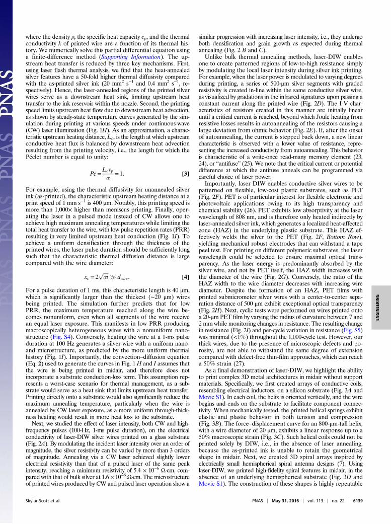
frequency pulses (100-Hz, 1-ms pulse duration), on the electricalconductivity of laser-DIW silver wires printed on a glass substrate(Fig. 2A). By modulating the incident laser intensity over an order ofmagnitude, the silver resistivity can be varied by more than 3 ordersof magnitude. Annealing via a CW laser achieved slightly lowerelectrical resistivity than that of a pulsed laser of the same peakintensity, reaching a minimum resistivity of 5.4 × 10⁻⁶ Ω·cm, com-pared with that of bulk silver at 1.6 × 10⁻⁶Ω·cm. The microstructureof printed wires produced by CW and pulsed laser operation show a
similar progression with increasing laser intensity, i.e., they undergoboth densification and grain growth as expected during thermalannealing (Fig. 2 B and C).Unlike bulk thermal annealing methods, laser-DIW enables
one to create patterned regions of low-to-high resistance simplyby modulating the local laser intensity during silver ink printing.For example, when the laser power is modulated to varying degreesduring printing, a series of 500-μm silver segments with gradedresistivity is created in-line within the same conductive silver wire,as visualized by gradations in the infrared signatures upon passing aconstant current along the printed wire (Fig. 2D). The I-V char-acteristics of resistors created in this manner are initially linearuntil a critical current is reached, beyond which Joule heating fromresistive losses results in autoannealing of the resistors causing alarge deviation from ohmic behavior (Fig. 2E). If, after the onsetof autoannealing, the current is stepped back down, a new linearcharacteristic is observed with a lower value of resistance, repre-senting the increased conductivity from autoannealing. This behavioris characteristic of a write-once read-many memory element (23,24), or “antifuse” (25). We note that the critical current or potentialdifference at which the antifuse anneals can be programmed viacareful choice of laser power.Importantly, laser-DIW enables conductive silver wires to be
patterned on flexible, low-cost plastic substrates, such as PET(Fig. 2F). PET is of particular interest for flexible electronic andphotovoltaic applications owing to its high transparency andchemical stability (26). PET exhibits low absorptivity at the laserwavelength of 808 nm, and is therefore only heated indirectly bylaser-annealed silver ink, which generates a localized heat-affectedzone (HAZ) in the underlying plastic substrate. This HAZ ef-fectively welds the silver to the PET (Fig. 2F, Bottom Row),yielding mechanical robust electrodes that can withstand a tapepeel test. For printing on different polymeric substrates, the laserwavelength could be selected to ensure maximal optical trans-parency. As the laser energy is predominantly absorbed by thesilver wire, and not by PET itself, the HAZ width increases withthe diameter of the wire (Fig. 2G). Conversely, the ratio of theHAZ width to the wire diameter decreases with increasing wirediameter. Despite the formation of an HAZ, PET films withprinted submicrometer silver wires with a center-to-center sepa-ration distance of 500 μm exhibit exceptional optical transparency(Fig. 2H). Next, cyclic tests were performed on wires printed ontoa 20-μm PET film by varying the radius of curvature between 7 and2 mmwhile monitoring changes in resistance. The resulting changein resistance (Fig. 2I) and per-cycle variation in resistance (Fig. S5)was minimal (<1%) throughout the 1,000-cycle test. However, ourthick wires, due to the presence of microscopic defects and po-rosity, are not able to withstand the same degree of extensioncompared with defect-free thin-film approaches, which can reacha 50% strain (27).As a final demonstration of laser-DIW, we highlight the ability
to print complex 3D metal architectures in midair without supportmaterials. Specifically, we first created arrays of conductive coils,resembling electrical inductors, on a silicon substrate (Fig. 3A andMovie S1). In each coil, the helix is oriented vertically, and the wirebegins and ends on the substrate to facilitate component connec-tivity. When mechanically tested, the printed helical springs exhibitelastic and plastic behavior in both tension and compression(Fig. 3B). The force–displacement curve for an 800-μm-tall helix,with a wire diameter of 20 μm, exhibits a linear response up to a50% macroscopic strain (Fig. 3C). Such helical coils could not beprinted solely by DIW, i.e., in the absence of laser annealing,because the as-printed ink is unable to retain the geometricalshape in midair. Next, we created 3D spiral arrays inspired byelectrically small hemispherical spiral antenna designs (7). Usinglaser-DIW, we printed high-fidelity spiral features in midair, in theabsence of an underlying hemispherical substrate (Fig. 3D andMovie S1). The construction of these shapes is highly repeatable
Skylar-Scott et al. PNAS | May 31, 2016 | vol. 113 | no. 22 | 6139
ENGINEE
RING
leading to uniform spiral arrays (Fig. 3 D, ii and iii). As a finalexample, we show the construction of arbitrary 3D shapes, suchas a butterfly, formed by printing multiple woven curvilinear wiresthat depart from the underlying substrate (Fig. 3E and Movie S1).Interestingly, these curvilinear structures can be printed on flexiblePET substrates, and by virtue of the strong adhesion at the silverwire–substrate interface resulting from HAZ formation, thesestructures can readily withstand cyclic bending of the substrate(Fig. 3 F and G).In summary, we have demonstrated a method of printing
planar and 3D metal architectures that combines laser-assistedannealing with direct writing of concentrated viscoelastic inks. Ourapproach is uniquely capable of printing elastic, complex curvi-linear metal wires in free space on low-cost plastic substrates.Furthermore, we have patterned silver wires with tunable electricalresistivity, enabling the programmable patterning of conductive,resistive, and hybrid elements. The ability to print high-resolution,functional metal electrodes and complex structures on demand
may open up new avenues for creating customized electronics,MEMs, and biomedical devices.
MethodsSilver Ink Synthesis. The silver nanoparticle ink is synthesized using a protocolsimilar to that previously described (1). Briefly, 0.9 g of a 25% (wt/v) solutionof 50 kDa poly(acrylic acid) (Polysciences Inc.) in water and 1.8 g of a 50%(wt/v) solution of 5 kDa poly(acrylic acid) (Polysciences Inc.) are dissolved into50 g of distilled water in a clean 500-mL Erlenmeyer flask. Forty grams ofdiethanolamine (Sigma-Aldrich) is then added, and the solution is allowed toreturn to room temperature while stirring at 300 rpm using a 1-inch stir bar.In a second clean flask, 20 g of silver nitrate (Sigma-Aldrich) is dissolved in 20 gof distilled water and the solution is allowed to return to room temperature,before adding the solution to the contents of the first flask while stirring. Thesolution is covered and stirred for 24 h. During this time, the solution turns fromcolorless to a clear, pale brown color as silver nanoparticles precipitate outunder the reducing conditions. After 24 h, the nanoparticles are ripened byincreasing the temperature to 75 °C for 2 h. The solution is then cooled to roomtemperature. Next, we rapidly add 300 mL of ethanol to the solution, whilestirring, to precipitate the nanoparticles. After 5 min of additional stirring, the
Fig. 2. Electrical conductivity and nanostructure of laser-annealed silver wires. (A) Silver resistivity decreases with increasing laser intensity. The red linerepresents the resistivity of bulk silver metal. Microstructure of silver wires annealed by (B) CW and (C) pulsed (1-ms, 100-Hz) laser illumination. Numbersindicate peak illumination intensity in kW/cm2. [Scale bars, 10 μm (C, i), 100 nm (C, ii).] (D) A varying laser intensity profile (Top) results in corresponding IRemissions from resistive elements as current is passed through the wire. Each resistor is ∼500 μm in length. (E) I-V characteristics of two resistors formed atdifferent laser intensities. Current is stepped up (unfilled) to a certain level, and then stepped down (filled). (F) SEM images of various diameter wires laserannealed onto PET films. (Top Row) Top view, false colored to reveal the HAZ extending from the printed silver wires. (Scale bar, 5 μm.) (Middle Row) Obliqueviews of printed silver wires. (Bottom Row) Magnified images of the interface between the printed silver (Ag) wire and PET substrate. (G) The width ofthe HAZ (black line) and the ratio of the HAZ width and the silver wire width (red line) vary with the diameter of the printed and annealed wires. Five wiresare tested for each diameter. (H) An array of silver wires, with submicrometer widths, is printed onto a transparent PET film across a 1-cm2 area, using a wirespacing distance of 500 μm. The resulting film, indicated by the white dashed line, remains transparent. (I) Cyclic testing of the electrical resistance of 3- and10-μm silver wires printed onto a 20-μm-thick PET film. The radius of curvature alternates between 2 and 7 mm. The graph shows the variation of resistanceafter n cycles (Rn) normalized to the initial resistance before cyclic testing (R0). Three wires are tested for each condition.
6140 | www.pnas.org/cgi/doi/10.1073/pnas.1525131113 Skylar-Scott et al.
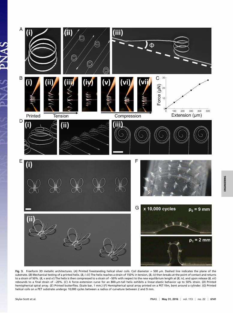
Fig. 3. Freeform 3D metallic architectures. (A) Printed freestanding helical silver coils. Coil diameter = 500 μm. Dashed line indicates the plane of thesubstrate. (B) Mechanical testing of a printed helix. (B, i–iii) The helix reaches a strain of 150% in tension, (B, iv) then breaks at the point of contact and returnsto a strain of 50%. (B, v and vi) The helix is then compressed to a strain of −50% with respect to the new equilibrium length at (B, iv), and upon release (B, vii)rebounds to a final strain of −20%. (C) A force–extension curve for an 800-μm-tall helix exhibits a linear-elastic behavior up to 50% strain. (D) Printedhemispherical spiral array. (E) Printed butterflies. (Scale bar, 1 mm.) (F) Hemispherical spiral array printed on a PET film, bent around a cylinder. (G) Printedhelical coils on a PET substrate undergo 10,000 cycles between a radius of curvature between 2 and 9 mm.
Skylar-Scott et al. PNAS | May 31, 2016 | vol. 113 | no. 22 | 6141
ENGINEE
RING
nanoparticles are allowed to settle under quiescent conditions. The supernatantis decanted away, and the silver nanoparticle sediment is transferred quickly viaa spatula into a separate 50-mL conical tube, ensuring that the suspension doesnot dry. The nanoparticles are then centrifuged at ∼13,000 g for 20 min into adense pellet, and the supernatant is discarded. The nanoparticles are then sus-pended again by adding 15 mL of water followed by vigorous vortexing. Thesuspension is filtered through a 5-μm syringe filter, then split into two 50-mLconical tubes before adding 35 mL of ethanol into each tube. The nano-particles are allowed to settle for 20 min before decanting the supernatant. Thenanoparticle suspension in one conical tube is transferred to the other by use ofa spatula before compacting the silver nanoparticles by centrifugation at 13,000 gfor 20 min. The nanoparticle pellet is then transferred out of the conical tubeusing a spatula, and placed in a jar to be mixed in a planetary mixer (ThinkyCorp.). The ink is then transferred via spatula into a 3-mL syringe (Nordson EFD)and centrifuged for 10min at 4,000 g to remove trapped air. The syringe is thenplaced into an HP3 high-pressure dispensing adaptor (Nordson EFD), connectedto a variable pressure supply (Nordson EFD), and a 2-inch-long glass nozzle witheither a 10- or 1-μm inner diameter is added to the syringe (World PrecisionInstruments). The syringe and high-pressure adaptor are mounted onto thelaser microscope and aligned with the focused laser spot.
Focused Laser and Ink Printhead Design. A 5-W, 808-nm CW diode laser(Shanghai Laser & Optics Century Co. Ltd.) is connected to the laser microscopeby means of a 200-μm multimode optical fiber (Thorlabs Inc.), and collimatedvia a 0.26-N.A., 11.07-mm collimating lens. The collimated beam is magnified 2×by a telescope consisting of a pair of IR antireflective achromatic doublet lenses(Thorlabs Inc.), and focused to a 100-μm spot using a 0.16-N.A., 12.43-mmworking distance aspheric objective lens. The laser focus spot possesses a uni-form, top-hat intensity distribution. The laser path includes a short-pass 750-nmdichroic mirror (Edmund Optics) that reflects the IR laser light, and transmitsvisible light collected by the objective to a camera (Imaging DevelopmentSystems, IDS) that serves as an alignment microscope. Importantly, to facilitatelaser–nozzle alignment, the dichroic mirror is selected to enable a small amountof IR light to be transmitted (<1%) to enable visualization of the substrate-reflected laser light with the top alignment camera. The entire optical setup ismounted on an optical breadboard, which itself is mounted onto an x–y–ztranslating 3D printing gantry (Aerotech Inc.). The laser diode driver ismodulated by a square-wave signal derived from either a waveform gen-erator (Keysight) or a National Instruments NI-6211, to enable the precisevariation of the laser pulse power, frequency, and duration.
To align the laser and ink deposition nozzle for printing, the laser is firstfocused onto the substrate by observing the laser spot on the alignment
camera. Next, x, y, and z micrometers are used to move the silver ink syringeand nozzle relative to the focused laser spot. A separate side camera (IDS) isused to aid this process. For omnidirectional printing, the nozzle is typicallyplaced ∼100 μm away from the laser spot. To begin printing, the silver ink isextruded through the nozzle by applying pressure (typically 150–200 psi),and the printer is translated in x, y, and z.
Rotary Stage Alignment. For freeform 3D printing, a rotary stage is used formounting the sample to enable the construction of curved lines. The rotarystage is positioned directly underneath the laser microscope. To identify thecenter of rotation, the laser is focused on the top surface of a glass slidecolored with a permanent marker. As the stage is rotated through 360°, thelaser spot ablates the permanent marker, tracing a circle whose center lies atthe center of rotation. The center of rotation is then supplied to a customMATLAB script that converts a series of x–y–z Gcode commands into a newset of commands in x–y–z, and θ.
Conductivity Measurements. Four 75-mm electrodes, consisting of gold stripes,are patterned onto a 75-mm × 25-mm glass slide by sputter coating. Next,linear wires are printed perpendicular to the stripes and a four-point probeis used to measure resistance between the center two stripes, separated by6.35 mm. To calculate electrical resistivity, their cross-sectional areas aremeasured by image analysis of scanning electron micrographs of cut wires.
Cyclic Mechanical Testing. Three-centimeter-long silver wires were printed usinglaser-DIW onto a 20-μm-thick PET substrate. After printing, one end of the film isaffixed to a stationary point and the other end is affixed to a point on an x–y–ztranslating gantry. Alligator clips and a resistance meter are used to monitorchanges in resistance. Before cyclic testing, the gantry is moved toward thestationary point, imparting a small initial curvature on the wire, and the initialresistance R0 is recorded. Next, the gantry is translated toward and away fromthe stationary point to flex the film to a radius of curvature of 2 mm, whilecontinuously monitoring the resistance.
ACKNOWLEDGMENTS. The authors thank James Weaver and Lori Sandersfor their assistance with imaging and photography, and Dr. Bok Y. Ahn andKundan Chaudhary for helpful discussions. This work is part of the “Light-Material Interactions in Energy Conversion” Energy Frontier Research Centerfunded by the US Department of Energy, Office of Science, Office of BasicEnergy Sciences under Award DE-SC0001293.
1. Ahn BY, et al. (2009) Omnidirectional printing of flexible, stretchable, and spanningsilver microelectrodes. Science 323(5921):1590–1593.
2. Xu S, et al. (2015) Assembly of micro/nanomaterials into complex, three-dimensionalarchitectures by compressive buckling. Science 347(6218):154–159.
3. Kim D-H, et al. (2008) Materials and noncoplanar mesh designs for integrated circuitswith linear elastic responses to extreme mechanical deformations. Proc Natl Acad SciUSA 105(48):18675–18680.
4. Pfeiffer C, Xu X, Forrest SR, Grbic A (2012) Direct transfer patterning of electricallysmall antennas onto three-dimensionally contoured substrates. Adv Mater 24(9):1166–1170.
5. Chang S, Sivoththaman S (2006) A tunable rf MEMS inductor on silicon incorporatingan amorphous silicon bimorph in a low-temperature process. IEEE Electron Device Lett27(11):905–907.
6. Huang W, et al. (2012) On-chip inductors with self-rolled-up SiNx nanomembranetubes: A novel design platform for extreme miniaturization. Nano Lett 12(12):6283–6288.
7. Adams JJ, Slimmer SC, Lewis JA, Bernhard JT (2015) 3D-printed spherical dipole an-tenna integrated on small RF node. Electron Lett 51(9):661–662.
8. Hu J, Yu M-F (2010) Meniscus-confined three-dimensional electrodeposition for directwriting of wire bonds. Science 329(5989):313–316.
9. Ching NNH, Wong HY, Li WJ, Leong PHW, Wen Z (2002) A laser-micromachined multi-modal resonating power transducer for wireless sensing systems. Sens Actuators APhys 97-98:685–690.
10. Felton S, Tolley M, Demaine E, Rus D, Wood R (2014) A method for building self-folding machines. Science 345(6197):644–646.
11. Gansel JK, et al. (2009) Gold helix photonic metamaterial as broadband circular po-larizer. Science 325(5947):1513–1515.
12. Soukoulis CM, Wegener M (2010) Optical metamaterials–more bulky and less lossy.Science 330(6011):1633–1634.
13. Soukoulis CM, Wegener M (2011) Past achievements and future challenges in thedevelopment of three-dimensional photonic metamaterials. Nat Photonics 5(9):523–530.
14. Xu L, et al. (2014) 3D multifunctional integumentary membranes for spatiotemporalcardiac measurements and stimulation across the entire epicardium. Nat Commun 5:3329.
15. Ko HC, et al. (2008) A hemispherical electronic eye camera based on compressiblesilicon optoelectronics. Nature 454(7205):748–753.
16. Çetin B, Kang Y, Wu Z, Li D (2009) Continuous particle separation by size via AC-dielectrophoresis using a lab-on-a-chip device with 3-D electrodes. Electrophoresis30(5):766–772.
17. Bae S, et al. (2010) Roll-to-roll production of 30-inch graphene films for transparentelectrodes. Nat Nanotechnol 5(8):574–578.
18. Park S-C, et al. (2015) Millimeter thin and rubber-like solid-state lighting modulesfabricated using roll-to-roll fluidic self-assembly and lamination. Adv Mater 27(24):3661–3668.
19. Deng B, et al. (2015) Roll-to-roll encapsulation of metal nanowires between grapheneand plastic substrate for high-performance flexible transparent electrodes. Nano Lett15(6):4206–4213.
20. Perelaer J, Hendriks CE, de Laat AWM, Schubert US (2009) One-step inkjet printing ofconductive silver tracks on polymer substrates. Nanotechnology 20(16):165303.
21. Lessing J, et al. (2014) Inkjet printing of conductive inks with high lateral resolutionon omniphobic “R(F) paper” for paper-based electronics and MEMS. Adv Mater26(27):4677–4682.
22. Ladd C, So J-H, Muth J, Dickey MD (2013) 3D printing of free standing liquid metalmicrostructures. Adv Mater 25(36):5081–5085.
23. Möller S, Perlov C, Jackson W, Taussig C, Forrest SR (2003) A polymer/semiconductorwrite-once read-many-times memory. Nature 426(6963):166–169.
24. Nilsson H-E, et al. (2011) Printed write once and read many sensor memories in smartpackaging applications. IEEE Sens J 11(9):1759–1767.
25. Allen ML, et al. (2008) Electrical sintering of nanoparticle structures. Nanotechnology19(17):175201.
26. Kaltenbrunner M, et al. (2012) Ultrathin and lightweight organic solar cells with highflexibility. Nat Commun 3:770.
27. Lu N, Wang X, Suo Z, Vlassak J (2007) Metal films on polymer substrates stretchedbeyond 50%. Appl Phys Lett 91(22):221909.
28. Skylar-Scott MA, Gunasekaran S (2015) Laser-DIW GCode Conversion. Available atwww.mathworks.com/matlabcentral/fileexchange/54425-laser-diw-gcode-conversion,MATLAB Central File Exchange. Accessed December 10, 2015.
29. Churchill SW, Chu HHS (1975) Correlating equations for laminar and turbulent freeconvection from a horizontal cylinder. Int J Heat Mass Transfer 18(9):1049–1053.
6142 | www.pnas.org/cgi/doi/10.1073/pnas.1525131113 Skylar-Scott et al.


![Direct Ink Writing Technology (3D Printing) of Graphene ......1. Introduction A ceramic is a nonmetallic, inorganic solid [1], which has exceptional and diverse physical and chemical](https://img.pdfslide.us/doc/110x75/6008081a3be72d6b690ef6fe/direct-ink-writing-technology-3d-printing-of-graphene-1-introduction.jpg)