Embed Size (px)
Citation preview

ITBW07 R. Frey 1
ECal with Integrated ElectronicsRay Frey, U of Oregon
Ongoing R&D Efforts:
• CALICE silicon-tungsten ECal – 2 parallel efforts: Technology Prototype “Eudet Module” (integrated electronics) Physics Prototype currently in test beam (electronics external)
• MAPS ECal Led by a sub-group of CALICE More recent – needs some proof of principle work before test beams
• “U.S.” silicon-tungsten ECal Has developed only an integrated approach from the start

ITBW07 R. Frey 2
Goal of this R&D
• The physics case implies a highly segmented “imaging calorimeter” with modest EM energy resolution Si-W
• The key to making this practical is a highly integrated electronic readout:
• readout channel count = pixel count / 1000
• requires low power budget (passive cooling)
• must handle the large dynamic range of energy depositions (few thousand) with excellent S/N
• This takes some time to develop (getting close).
• Testing in beams will be crucial.
Design a practical ECal which (1) meets (or exceeds) the physics requirements (2) with a technology that would actually work at the ILC.

3
The “U.S.” Silicon-Tungsten ECal R&D
Currently optimized for the SiD concept
Baseline configuration:
• transverse segmentation: 12 mm2 pixels
• longitudinal: (20 x 5/7 X0) + (10 x 10/7 X0) 17%/sqrt(E)
• 1 mm readout gaps 13 mm effective Moliere radius

ITBW07 R. Frey 4
US Si-W ECal R&D Collaboration
M. Breidenbach, D. Freytag, N. Graf, R. Herbst, G. Haller, J. Jaros
Stanford Linear Accelerator Center
J. Brau, R. Frey, D. Strom,
M. Robinson, A.Tubman
U. Oregon
V. Radeka
Brookhaven National Lab
B. Holbrook, R. Lander, M. Tripathi
UC Davis
S. Adloff, F. Cadoux, J. Jacquemier, Y. Karyotakis
LAPP Annecy
• KPiX readout chip
• downstream readout
• detector, cable development
• mechanical design and integration
• detector development
• readout electronics
• readout electronics
• cable development
• bump bonding
• mechanical design and integration

ITBW07 R. Frey 5
Technological prototype : “EUDET module”
Front-end ASICs embedded in detector Very high level of integration Ultra-low power with pulsed mode FLC_TECH1 ASIC prototype in 0.35 µm SiGe
All communications via edge 4,000 ch/slab, minimal room, access, power small data volume (~ few 100 kbyte/s/slab)
« Stitchable motherboards »
Elementary motherboard ‘stitchable’ 24*24 cm ~500 ch. ~8 FE ASICS
©H. Videau (LLR)

6

ITBW07 R. Frey 7
“Imaging Calorimeters”
A highly segmented ECal is part of the overall detector tracking (charged and neutrals)
ITBW07 R. Frey 8
Segmentation requirement
• In general, we wish to resolve individual photons in jets, tau decays, etc.• The resolving power depends on Moliere radius and segmentation.
• We want segmentation significantly smaller than Rm
Two EM-shower separability in LEP data with the OPAL Si-W LumCal (David Strom)

9
Silicon detector layout and segmentation – U.S.
(KPiX)
• Silicon is easily segmented
• KPiX readout chip is designed for 12 mm2 pixels (1024 pixels for 6 inch wafer)
• Cost nearly independent of seg.
• Limit on seg. from chip power (2 mm2 )
Fully functional prototype (Hamamatsu)
10Konstantin Stefanov, CCLRC Rutherford Appleton Laboratory 10ECFA 2006, Valencia 10ECFA 2006, Valencia
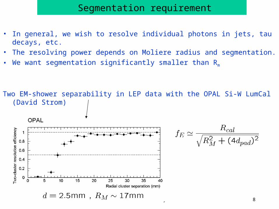
Features of the Monolithic Active Pixel Sensor (MAPS) -based calorimeter:
● Binary readout: hit or no hit per pixel (1-bit ADC)
● Pixels are small enough to ensure low probability of more than one particle passing
through a pixel
● With ~100 particles/mm2 in the shower core and 1% probability of double hit the
pixel size should be ~40 μm×40 μm
● Current design with 50 μm×50 μm pixels – see Yoshi Mikami’s talk
● Timestamps and hit pixel numbers stored in memory on sensor
● Information read out in between trains
● Total number of ECAL pixels around 8×10¹¹: Terapixel system
● Only monolithic designs can cope with that number of pixels – hence MAPS
MAPS-based ECAL Design
Konstantin Stefanov
On behalf of
J. Crooks, P. Dauncey, A.-M. Magnan, Y. Mikami, R. Turchetta, M. Tyndel, G. Villani, N. Watson, J. Wilson
Valencia

ITBW07 R. Frey 11
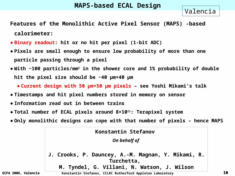
Critical parameter for RM is the gap between layers
ITBW07 R. Frey 12
Tungsten
Tungsten
Si Detector
KPix
Kapton
Kapton Data (digital) Cable
Bump Bonds
Metallization on detector from KPix to cable
Thermal conduction adhesive
Heat Flow
US Si-W readout gap schematic cross section
Gap 1 mm

ITBW07 R. Frey 13
Data Concentrator
“Longitudinal” Data Cable
“Transverse” Data Cable
Detectors
Readout Chip “KPix”
Tungsten Radiator
Locating Pins
Conceptual Schematic – Not to any scale!!!
~ 1m

ITBW07 R. Frey 14
EUDET - Detector slab (2)
Exploded viewChip « inside »
Connection between 2 PCB
7 “unit” PCB“end” PCBde La Taille
ITBW07 R. Frey 15
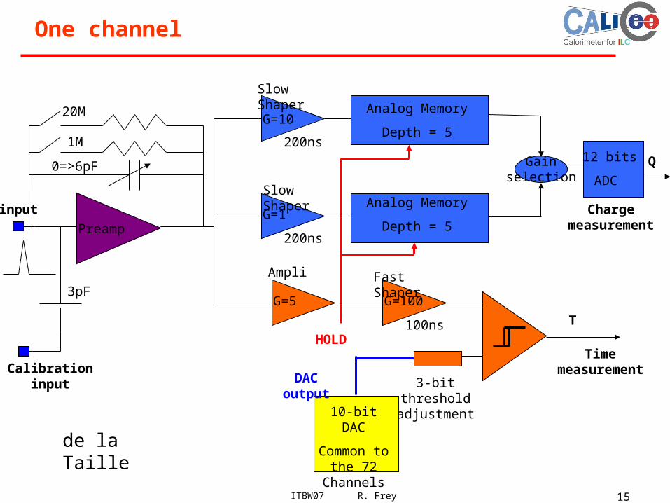
One channel
20M
1M 200ns
G=10
G=1
200ns
Analog Memory
Depth = 5
Analog Memory
Depth = 5
G=100G=5
12 bits
ADC
Gain selection
0=>6pF
3-bit threshold adjustment
10-bit DAC
Common to the 72
Channels
T100ns
DAC output
Q
HOLD
Preamp
Ampli
Slow Shaper
Slow Shaper
Fast Shaper
Time measurement
Charge measurement
3pF
Calibration input
input
de la Taille

ITBW07 R. Frey 16
SKIROC for W-Si ECAL
Silicon Kalorimeter Integrated Read Out Chip (Nov 06) 36 channels with 16 bits Preamp + bi-gain shaper +
autotrigger + analog memory + Wilkinson ADC Digital part outside in a FPGA for lack of time and increased
flexibility

ITBW07 R. Frey 17
KPiX chip
One channel of 1024
Si pixel
Dynamic gain select
Event trigger
Leakage current subtraction
calibration
Storage until end of train.
Pipeline depth presently is 4
13 bit A/D

ITBW07 R. Frey 18
KPiX Cell 1 of 1024
64-channel prototypes:
• v1 delivered March 2006
• v4 delivered Jan 16, 2007
It’s a complicated beast – may need a v5 before going to the full 1024-channel chip ?

ITBW07 R. Frey 19
Dynamic Range
KPiX-2 prototype on the bench
Max signal: 500 GeV electron
1 MIP (4 fC)

ITBW07 R. Frey 20
Power Pulsing
de La Taille
ITBW07 R. Frey 21
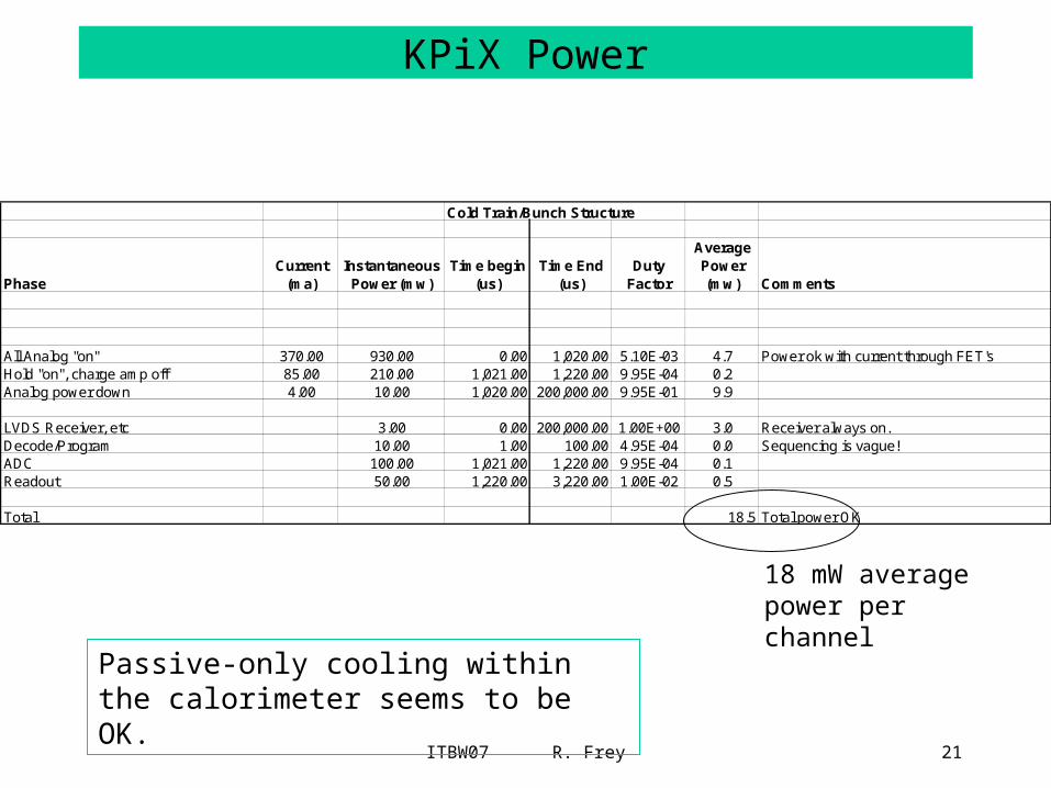
KPiX Power
Cold Train/Bunch Structure
PhaseCurrent
(ma)Instantaneous
Power (mw)Time begin
(us)Time End
(us)Duty
Factor
Average Power (mw) Comments
All Analog "on" 370.00 930.00 0.00 1,020.00 5.10E-03 4.7 Power ok with current through FET'sHold "on", charge amp off 85.00 210.00 1,021.00 1,220.00 9.95E-04 0.2Analog power down 4.00 10.00 1,020.00 200,000.00 9.95E-01 9.9
LVDS Receiver, etc 3.00 0.00 200,000.00 1.00E+00 3.0 Receiver always on.Decode/Program 10.00 1.00 100.00 4.95E-04 0.0 Sequencing is vague!ADC 100.00 1,021.00 1,220.00 9.95E-04 0.1Readout 50.00 1,220.00 3,220.00 1.00E-02 0.5
Total 18.5 Total power OK
Passive-only cooling within the calorimeter seems to be OK.
18 mW average power per channel

ITBW07 R. Frey 22
prototype Si detector studies
ITBW07 R. Frey 23
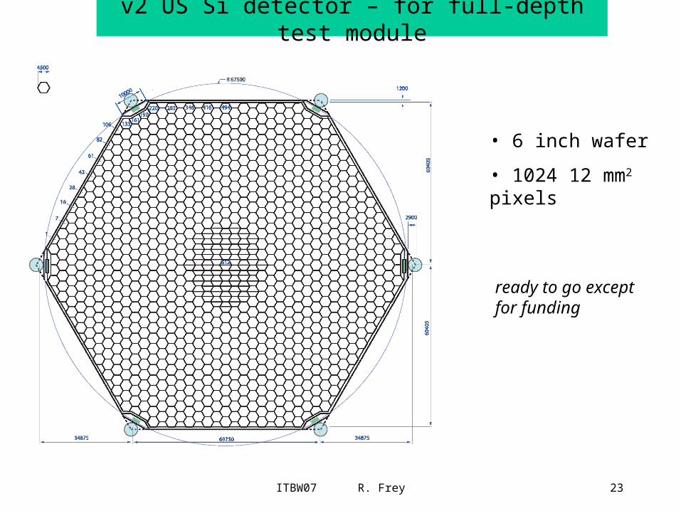
v2 US Si detector – for full-depth test module
• 6 inch wafer
• 1024 12 mm2 pixels
ready to go except for funding

24
R&D Milestones – US Si-W
I. Connect (bump bond) prototype KPiX to prototype detector with associated readout cables, etc
• Would benefit from test beam (SLAC?) - 2007
• A “technical” test
II. Fabricate a full-depth ECal module with detectors and KPiX-1024
readout * – functionally equivalent to the real detector
• Determine EM response in test beam – 2008
• Ideally a clean 1-30 GeV electron beam (SLAC?)
III. Test with an HCal module in hadron test beam (FNAL?) – 2008-?
• Test/calibrate the hadron shower simulations; measure response
IV. Pre-assembly tests of actual ECal modules in beam – >2010
pending funding
25
Test beam requirements (wishes)
For the initial testing (milestone I):• nearly anything will do
For the EM response test (milestone II)• Dedicated electron or positron beam
1 – 30 GeV Rate down to one (or zero) particles per bucket Well-localized (1 cm) beam
• Timing: KPiX can run in an externally triggered mode
• Buffer depth of 4• Requires about 3-6 ms to complete a DAQ cycle expect dead time
For the test in the hadron beam line (milestone III):• Sufficient quantity of electrons (low to high energy) to verify carry-over of
response from the EM test, otherwise program mostly defined by HCal• Will need a veto of transverse shower leakage out of the ECal
(scintillators)

ITBW07 R. Frey 26
Summary
• The R&D leading to an “ILC-ready” Si-W ECal technology is progressing well. The MAPS concept provides an interesting alternative
• The Si-W R&D should result in full-depth modules which will require test beam evaluation The CALICE Eudet module (30 layers x 12cm x 150cm) - 2009 The US Si-W module (30 layers x 16cm x 16cm) - 2008*
• These highly segmented, analog devices should provide an interesting test for simulation modeling of (early developing) hadron showers.
• May be crucial for understanding the HCal
• As we transition from R&D to “D” (>2010), there will certainly be a need for pre-assembly tests of the real ECal modules.