Embed Size (px)
Citation preview
Session 7.2 1
IP Authoring and Integration for HW/SW Co-Design and Reuse - Lessons Learned
Frank Schirrmeister, Martin Meindl and Stan Krolikoski Cadence Design Systems, San Jose, CA, USA
Abstract
The development process within the electronics design chain is adjusting to requirements caused by the complexity of today’s and tomorrow’s System on Chip (SoC) designs. Design for re-use is becoming a standard practice, sets new requirements for next generation tools and is leading to organizational changes within companies.
Since 1998, we have discussed design methodology and tool requirements that would allow designers to create IP-dominated (SOC) devices at the system level of abstraction. This paper will review lessons learned in applying the proposed techniques to real design problems in the context of platform-based design.
Furthermore this paper will review different techniques for IP Authoring required for modern SoC design. Different models of computation have to be supported to cover simulation and implementation of control, data flow and continuous time processing. Furthermore this paper will outline different techniques for IP Integration, focusing on early interaction within the design chain, between IP Creators and Integrators.
The paper will close with lessons learned from user experiences by analyzing and comparing different use models of IP authoring for re-use and IP integration at the system level. Besides the model requirements for representing the IP blocks themselves, different solutions for test bench authoring and re-usable verification environments will be shown as well.
1. Introduction
Design of electronic products is currently undergoing a profound revolution throughout all application fields. The complexity of automotive, wireless and multimedia applications has been exploding over the last couple of years and the productivity of design teams had difficulties to keep up with this trend. Now this trend is even further accelerated by the demand for convergence products combining the disciplines of several application domains. Typical examples are the convergence of wireless communications and video and audio processing capabilities, and of course the entry of wireless and multimedia applications into the car.
1.1. Market Drivers
Two trends were fairly obvious – the development of the cost of manufacturing and the complexity issues. For silicon providers the average cost of a high end ASSP and the cost of fabrication and masks have increased significantly. Looking at 5x to 10x times return on the development cost, formerly attractive chip volumes are likely not be able to satisfy the return on investment needs in the future. On the other hand the task of system houses to efficiently design and verify embedded systems grows exponentially as embedded systems increase in capability.
Facing these challenges designers are turning to new methodologies – integration platform based design and function-architecture co-design approaches driven from higher levels of abstraction at the system level.
In order for these two approaches to be applied to electronics design it has become obvious that new technologies need to be made available by EDA companies which allow design at a higher level of abstraction.
The current techniques of translating written, ambiguous specifications into register transfer level (RTL) descriptions for HW and C or assembler code for implementation SW are clearly running out of steam. Designers can verify at that level of abstraction the interaction of HW and SW using Co-Verification tools, the simulation speed for the amount of detail to be simulated at the complexity of today’s and tomorrow’s systems does not permit those techniques to make efficient design decisions regarding system partitioning etc.
1.2. Platform Based Design
The concept of platform-based design for systems on chip (SOC) allows semiconductor companies to capitalize of economy of scale for the silicon production. Several application instances of the same application area can be implemented on the same piece of silicon customizable and configurable using SW. The concept has been introduced in several publications, see [1], [2], [3] and [4].
A SOC integration platform is defined as a high productivity design environment, which specifically targets a product application domain, and which is based on a Virtual Component (VC) reuse, mix and match design methodology. Another definition of platform is “a family of architectures that satisfy a set of architectural constraints that are imposed to allow the re-use of HW and SW components”. Both of these definitions emphasize the concept of reuse, and also imply the creation of a family of derivative products based on a common platform HW-SW architecture.
Session 7.2
Platforms in general consist of a fixed HW kernel, usually containing major on-chip communications structures and buses, processors, memory controllers, and common HW and SW components such as a basic set of peripherals, their device drivers, and a configurable RTOS; and a variable component which allows for customization into a stream of derivative products. These derivatives are created by two fundamental methods:
• HW and/or SW virtual components, which have been pre-qualified as part of the integration platform to be suitable for integration into a derivative product, can be selected from a general library and used as-is.
• Appropriate HW and SW components are selected, which can be modified during integration into the derivative in order to meet system functionality.
The ideal in platform-based design allows derivatives to be constructed from true virtual components drawn from an IP library – reuse without modification. In this way, the analogy between PCB based design using standard off-the-shelf components and SOC platform-based design is nearly complete.
1.3. Function Architecture Co-Design
However, to complete the PCB analogy of reuse without modification, we need to find a design method for SOC design as simple and productive as classical PCB design in which components can be easily swapped in and out physically, and use of physical cuts and jumpers allowed rapid re-wiring of these components into the overall system. Unfortunately, integrated SOC devices, like all ICs, do not lend themselves to these simple physical methods of system design. We must find a better method, and one that inherently supports the platform and derivative design concept. This is the approach we call function-architecture co-design, which has originally been introduced in [5].
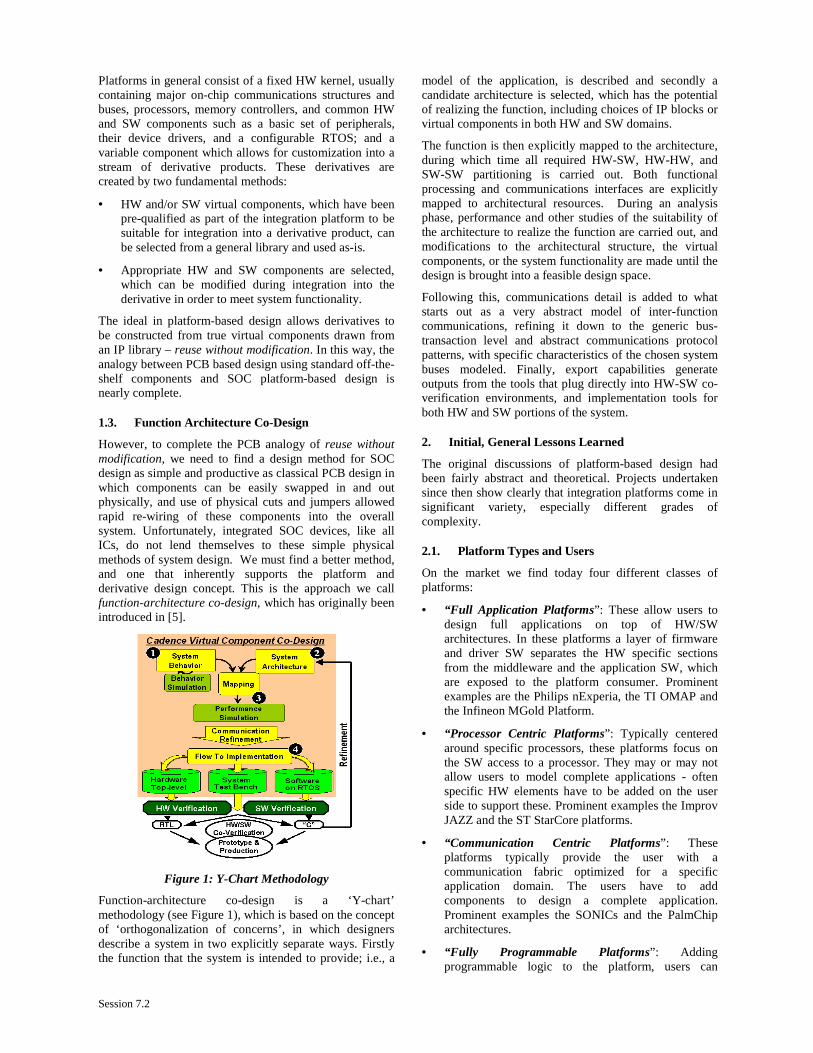
Figure 1: Y-Chart Methodology
Function-architecture co-design is a ‘Y-chart’ methodology (see Figure 1), which is based on the concept of ‘orthogonalization of concerns’, in which designers describe a system in two explicitly separate ways. Firstly the function that the system is intended to provide; i.e., a
model of the application, is described and secondly a candidate architecture is selected, which has the potential of realizing the function, including choices of IP blocks or virtual components in both HW and SW domains.
The function is then explicitly mapped to the architecture, during which time all required HW-SW, HW-HW, and SW-SW partitioning is carried out. Both functional processing and communications interfaces are explicitly mapped to architectural resources. During an analysis phase, performance and other studies of the suitability of the architecture to realize the function are carried out, and modifications to the architectural structure, the virtual components, or the system functionality are made until the design is brought into a feasible design space.
Following this, communications detail is added to what starts out as a very abstract model of inter-function communications, refining it down to the generic bus-transaction level and abstract communications protocol patterns, with specific characteristics of the chosen system buses modeled. Finally, export capabilities generate outputs from the tools that plug directly into HW-SW co-verification environments, and implementation tools for both HW and SW portions of the system.
2. Initial, General Lessons Learned
The original discussions of platform-based design had been fairly abstract and theoretical. Projects undertaken since then show clearly that integration platforms come in significant variety, especially different grades of complexity.
2.1. Platform Types and Users
On the market we find today four different classes of platforms:
• “Full Application Platforms”: These allow users to design full applications on top of HW/SW architectures. In these platforms a layer of firmware and driver SW separates the HW specific sections from the middleware and the application SW, which are exposed to the platform consumer. Prominent examples are the Philips nExperia, the TI OMAP and the Infineon MGold Platform.
• “Processor Centric Platforms”: Typically centered around specific processors, these platforms focus on the SW access to a processor. They may or may not allow users to model complete applications - often specific HW elements have to be added on the user side to support these. Prominent examples the Improv JAZZ and the ST StarCore platforms.
• “Communication Centric Platforms”: These platforms typically provide the user with a communication fabric optimized for a specific application domain. The users have to add components to design a complete application. Prominent examples the SONICs and the PalmChip architectures.
• “Fully Programmable Platforms”: Adding programmable logic to the platform, users can

Session 7.2 3
customize the platform using both HW and SW. Prominent examples are the Triscend, Altera Excalibur and Xilinx P-FPGA Platforms combining dedicated processors and programmable logic.
The platform users vary from users expecting “shrink wrapped” platforms with complete HW and SW configurations to users who actually differentiate at all levels by adding SW routines and even adding in specific HW blocks tailored for a specific platform.
2.2. Traditional Integration Approaches
Figure 2 indicates the traditional approach of system integration as it is typically used today. Different parts of the system are developed using available IP Authoring techniques, which result in SW or HW implementations.
The integration of all those system blocks is done after the implementation of the different system blocks in Verilog; VHDL or C/Assembler code has been done. At this point in the design process all the essential partitioning decisions mentioned above have been done already using ad hoc techniques. Finding at this point, that a module, which is implemented in SW, really should have been implemented in HW for performance reasons, can become a pivotal point in the career of a project manager.
A system on silicon with a processor core, a complete MPEG-2 AV decoder and integrated memories runs at the RTL level easily 20- to 24 hours for the decoding of a PAL frame. This level of abstraction is clearly not suitable for the verification of audio and video synchronization effects, which often only happen after hundreds of frames. Furthermore have at this level implementations already committed to HW and SW and also the function and architecture of the design have been mixed. It is for economic reasons typically not possible to re-implement modules or even to consider a functional derivative at this point.
2.3. Design Flows revisited
From figure 2 it also easy to derive requirements for today’s design flows. It turns out that there is a distinct
difference between IP Authoring and IP Integration, a difference that has to be addressed by EDA tools.
At first the different IP blocks have to be implemented in an optimized fashion. In this process of “IP Authoring” designers would translate embedded system requirements into an abstract system level model. Abstract, un-timed C or C++ description techniques as used in SDL or Cadence SPW will ideally lead to an executable system level specification.
Figure 3: IP Authoring
These system level descriptions can be used to assess and analyze the suitability and configuration of algorithms used in the system context, for example the algorithms defining the channel decoding or the MAC layer in a cell-phone.
From this system level description the designer will then add implementation information which is required to refine the model from the abstract, un-clocked system level to the clocked implementation level. Again, Cadence SPW offers with the HW Design System [HDS] capabilities to support this design flow for HW. In the recent past C++ based techniques have been suggested for HW design as well. Together with implementation level class libraries they support C++ based design at the
Figure 2: Traditional System Integration
Session 7.2
clocked implementation level. Figure 3 depicts a generalized IP Authoring design flow for HW and SW.
For SW modules Telelogic TAU and Rational UML/RT support analogous techniques to derive from a system level SW description the actual SW implementation, which then can be directly used in an embedded system.
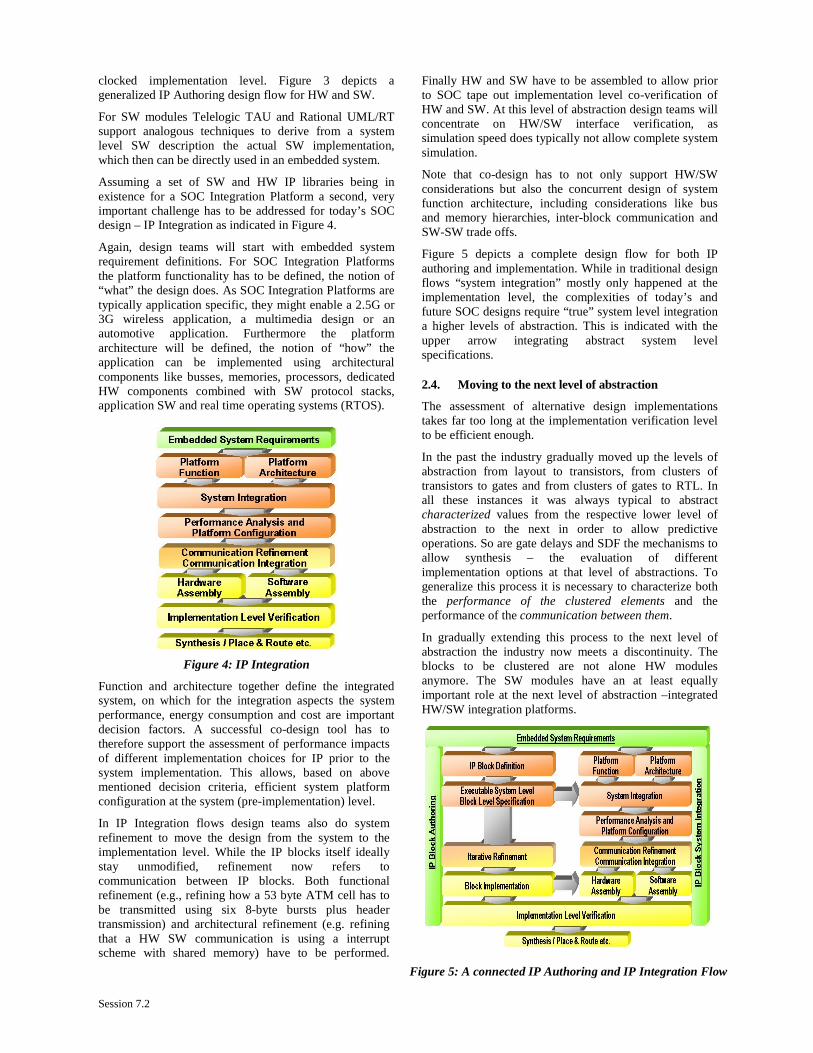
Assuming a set of SW and HW IP libraries being in existence for a SOC Integration Platform a second, very important challenge has to be addressed for today’s SOC design – IP Integration as indicated in Figure 4.
Again, design teams will start with embedded system requirement definitions. For SOC Integration Platforms the platform functionality has to be defined, the notion of “what” the design does. As SOC Integration Platforms are typically application specific, they might enable a 2.5G or 3G wireless application, a multimedia design or an automotive application. Furthermore the platform architecture will be defined, the notion of “how” the application can be implemented using architectural components like busses, memories, processors, dedicated HW components combined with SW protocol stacks, application SW and real time operating systems (RTOS).
Figure 4: IP Integration
Function and architecture together define the integrated system, on which for the integration aspects the system performance, energy consumption and cost are important decision factors. A successful co-design tool has to therefore support the assessment of performance impacts of different implementation choices for IP prior to the system implementation. This allows, based on above mentioned decision criteria, efficient system platform configuration at the system (pre-implementation) level.
In IP Integration flows design teams also do system refinement to move the design from the system to the implementation level. While the IP blocks itself ideally stay unmodified, refinement now refers to communication between IP blocks. Both functional refinement (e.g., refining how a 53 byte ATM cell has to be transmitted using six 8-byte bursts plus header transmission) and architectural refinement (e.g. refining that a HW SW communication is using a interrupt scheme with shared memory) have to be performed.
Finally HW and SW have to be assembled to allow prior to SOC tape out implementation level co-verification of HW and SW. At this level of abstraction design teams will concentrate on HW/SW interface verification, as simulation speed does typically not allow complete system simulation.
Note that co-design has to not only support HW/SW considerations but also the concurrent design of system function architecture, including considerations like bus and memory hierarchies, inter-block communication and SW-SW trade offs.
Figure 5 depicts a complete design flow for both IP authoring and implementation. While in traditional design flows “system integration” mostly only happened at the implementation level, the complexities of today’s and future SOC designs require “true” system level integration a higher levels of abstraction. This is indicated with the upper arrow integrating abstract system level specifications.
2.4. Moving to the next level of abstraction
The assessment of alternative design implementations takes far too long at the implementation verification level to be efficient enough.
In the past the industry gradually moved up the levels of abstraction from layout to transistors, from clusters of transistors to gates and from clusters of gates to RTL. In all these instances it was always typical to abstract characterized values from the respective lower level of abstraction to the next in order to allow predictive operations. So are gate delays and SDF the mechanisms to allow synthesis – the evaluation of different implementation options at that level of abstractions. To generalize this process it is necessary to characterize both the performance of the clustered elements and the performance of the communication between them.
In gradually extending this process to the next level of abstraction the industry now meets a discontinuity. The blocks to be clustered are not alone HW modules anymore. The SW modules have an at least equally important role at the next level of abstraction –integrated HW/SW integration platforms.
Figure 5: A connected IP Authoring and IP Integration Flow

Session 7.2 5
The elements to be characterized in this case now are at least twofold:
• Processing performance of the HW and SW modules. This is unlikely to be a simple parameter, one number. Instead this performance will depend on different states in the HW module and the chosen control path in a SW module.
• Communication performance between HW and SW modules. This will include all possible permutations. Direct interfaces between HW modules characterized with different performance depending on the chosen handshake protocol. Interfaces between SW modules using services provided by real time operating systems (RTOS). Finally, the different options of communication between SW and HW and vice versa need to be characterized. This includes for example interrupts which trigger SW from HW and protocols in which to be accessed HW can be programmed.
2.5. Cadence Virtual Component Co-Design
Function-architecture co-design, when linked to platform-based design, provides a sophisticated high productivity methodology.
In cooperation with major partners representing the application domains automotive, wireless and multimedia, Cadence Design Systems has over the last three years developed the Virtual Component Co-Design (VCC) tools through the Felix initiative (see also [3], [4], [6], [7], [8], [9] and [10]).
The resulting toolset - the VCC Environment - which was released in January 2000 after a considerable period of usage by technology partners and early adopters, is an environment for system level design facilitating function-architecture co-design, HW/SW co-design and Intellectual Property (IP) reuse techniques. VCC is enhancing the traditional design methodologies for IP Authoring (creation of IP) with a new set of IP Integration techniques, which allow the efficient design of initial and derivative products in convergence application fields.
3. The SOC Design Chain
Probably the most significant lesson learned has been the fact the interaction within the design chain determines the use-model of system-level tools like Cadence SPW and VCC.
There are several players involved in exchanging design data (see also [3]). Classical providers of Star-IP like ARM and MIPS provide their IP to system houses and SOC providers. This IP can be both HW, as for example in the case of processors, and SW as found in protocol stacks of wireless systems.
System Houses are on the top of the design chain with the need to articulate the system requirements to their various suppliers. SOC Providers attempt to match these system requirements with providing applications specific platforms based on their silicon and SW supporting the processor types available in their silicon technology.
Ideally the System Integrator wants to make integration decisions using a SOC platform provided by a semiconductor company as early as possible in the design cycle. Key design decisions that are taken at the system level include:
• Support for required new standards • Functional bandwidth, throughput, and latency
requirements • Communications resource bandwidth and latency,
modeled at abstract and detailed levels of refinement • Energy consumption and cost • SW task decomposition, messaging and priorities • How much of the platform reference design can be re-
used in the derivative-- as-is, or with modifications? • How much estimated margin is there in a derivative
design to handle unexpected issues during implementation?
EDA tools must support delivery of models at several levels of abstraction –from system-level to implementation.
4. Next Generation SOC Design Kits
Three part engagements have become the norm. Suppliers of IP and integration platforms interact with their system customers. Cadence has in these projects taken the role of a facilitator.
In order to allow efficient interaction within the design chain the different function and architecture components of a platform have to be delivered in library structures.
To support the different requirements of System Integrators each element has to be delivered at the appropriate levels of abstraction for different phases in the design process. A couple of examples are outlined in the next paragraphs.
4.1. HW Modules
The highest level of abstraction for modules, which end up to be implemented in HW, has to be a pure functional model, which allows function architecture co-design. This functional description can be articulated using tools like Cadence SPW, C++ or any description which can be wrapped in a OMI (IEEE 1499) interface.
For the actual HW implementation a set of performance models has to be provided, which allows the assessment, which specific HW implementation should be chosen. VCC supports these models through a simple Delay Scripting Language DSL.
At the implementation level the RTL function should be made available through OMI for co-simulation and co-verification.
The most detailed model in the design kit will be the actual RTL model plus synthesis constraints.
4.2. SW Modules
The highest level of abstraction for modules, which end up to be implemented in SW, has to be again a pure functional model, which allows function architecture co-
Session 7.2
design. This functional description can be articulated using tools like Telelogic TAU for SDL, C++ or any description which can be wrapped in a OMI (IEEE 1499) interface.
For the actual SW implementation a set of performance models has to be provided, which allows the assessment, which specific SW implementation should be chosen. VCC supports these models through a simple Delay Scripting Language DSL.
At the implementation level C can be again packed through OMI and made available for implementation level verification.
The most detailed model in the design kit can be the assembler model, potentially even hand-optimized.
4.3. Communication Models
The communication between arbitrary HW and SW modules has to be modeled for evaluation of performance impacts using architecture services as provided in the VCC Environment.
For implementation a synthesizable version of communication information can be made available which allows to move functions across HW /SW boundaries and automatically synthesize the interface afterwards. This process is called Communication Synthesis in the VCC environment.
4.4. RISC Processors
To enable SW estimation so called Virtual Processor Models can be provided, in the VCC Environment, which provide a characterization of the main instruction classes and allow the assessment of SW performance prior to implementation. Design decisions can be made at this level.
For actual verification ISS models have to be provided, which allow the object code execution on a processor for the purpose of functional verification and HW/SW Co-Verification
4.5. DSPs
To reflect the performance of tasks, which the DSP has been optimized for, the performance characterization as provided today in data books can be used in the VCC Environment in an executable fashion.
For actual verification ISS again models have to be provided, which allow the object code execution on a processor for the purpose of functional verification and HW/SW Co-Verification
4.6. Busses
For the actual performance evaluation the delay and arbitration of the bus can be characterized in the VCC Environment.
At the implementation level the detailed bus interface logic has to be available fully articulated.
4.7. Memories
For performance evaluation the memory access times and the information about burst modes etc. has to be provided.
At the implementation level detailed, typically C based models, which check set up and hold times and reflect the actual memory allocation accurately.
4.8. Real Time Operating Systems (RTOS)
At the performance evaluation level a RTOS has to reflect the access to the processor (arbitration policy) plus the performance impact of context switching, e.g. start, stop, suspend and resume times. Furthermore the number of interrupts and RTOS services like timer and semaphores need to be available for evaluation. At the implementation Co-Verification level the object code of the RTOS can be booted on an ISS.
5. IP Authoring Use Models
The Cadence Signal Processing Work system (SPW) provides an efficient IP authoring infrastructure for digital signal processing algorithms.
Initially researchers get started to explore new worlds, like we can see in the wireless communication space right now with its 4th generation, where datarates up to 100Mb and frequencies up to 66GHz are targeted. Ideas shape, standards start creating a marketplace and companies starting development. The products need to comply with the standards set before, differentiate by features to gain market acceptance and use resources efficiently to keep proper margins.
5.1. Research Phase
Scientists play with their ideas, on whiteboards, papers and create computer models to prove their ideas would work against a certain physical environment. They would use Cadence SPW to actually experiment with their preferred algorithms, analyze the results with SigCalc and plot and document their findings in papers they use at the next conference. Feedback goes into the refinement of the models, where ease of use, flexible-authoring paradigms likes to capture control, dataflow and time continuous domains is of essence. Experiments are mostly done in the floating domain; implementation is not a concern at all yet.
5.2. Top Down Product Development
New applications get visible, and industry predicts good business using the new standard. Development teams start working building reference models, introducing real channel effects and capture the performance data of a system, which should resemble the standard. The teams are building executable specifications, and bring on their own ideas for algorithms to address specific problems.
Cadence SPW is widely used in the communications and multimedia industry to capture those simulation models, in fact, Cadence and partners like NIST [22] do actually also provide those models. Cadence follows changes in the standards immediately and delivers the enhanced models
Session 7.2 7
to their respective customers ASAP, giving with this fast turnaround their customers the ability to concentrate on features they want use to differentiate. Getting a reference library gives a huge productivity boost and makes it easy for design teams to deliver on time [23].
5.3. Product Development Applying Reuse
Graphical, hierarchical parametrizable models written in C, C++, SystemC, UML or behavioral analog languages allow for the best modeling styles selected for the task in mind. In fact, if you have implemented a design piece in a previous project already for HW, would you voluntarily recode that block in C so it can be simulated together with other newly created models? Simulators are required which can execute various simulation domains together without giving a performance hit to the user.
They need to support standard interfaces like OMI [24] and should allow a free mix of C/C++/SystemC/VHDL/Verilog/VerilogA as the Cadence SPW/NC-Sim environment [25] does. Reuse of previously generated HW blocks would not be a problem, and also the RF design team and the Baseband engineers can easily explore the performance of their end to end system before they integrate the first prototype in the labs.
As the next step engineers now need to decide, which platform can deliver the right performance to realize the desired functionality.
6. IP Integration Use Models
The tool framework provided to users with the VCC environment has been designed in an open fashion and allows users to follow several types of use models.
6.1. General Top Down Design Exploration
Like the algorithmic exploration in IP Authoring techniques there is a lot of value in the exploration how systems connect and behave on different target architecture options. Ericsson reports in [11] their experience with HW/SW Co-Design and re-emphasizes the importance of separation of function and architecture. This enables much easier modification of designs at the system level and easier reuse of behavior and architecture virtual components. The ability to make ‘what-if’ kinds of changes in architectures and mappings is important to build understanding of the system under design. BMW reported at various occasions including [21] about their design space exploration efforts using VCC.
6.2. Top Down Platform Exploration
During the actual development of the platform trade of decisions have to be made. A system house will define a platform in which the architectural components are not yet bound to real implementations. This way trade offs between bus systems, memory hierarchies etc. can be analyzed and fed back to the development.
In contrast a semiconductor house will define a platform depending on the availability of architecture components in their portfolio. This use model is applied during the
development of an actual platform. The challenging part here is to define the range of application variants in an appropriate way. This range then directly translates into the amount of scalability within a platform.
6.3. Bottom Up Platform Characterization
Once a platform definition exists the different components can be characterized to reflect the implementation issues. Busses, RTOSs, processors etc. build the characterized components of a platform, which can be used by system houses as a target to map application variants to. ST Microelectronics reported in [18] about efforts to provide and characterize architectural components for consumption by internal and external customers. Philips reported in [12], [13] and [14] about efforts to characterize parts of a multimedia platform with a strong focus on the communication design.
6.4. Configuration of Characterized Platform
Having received a characterized platform the system house can map application derivatives to the platform and explore different alternatives. Magneti Marelli reports in [15] about their interaction with IP and architectural component providers. Motorola describes in [20] a similar use model. The platform has here not been formerly characterized except through the system-level design team. The BWRC also followed similar flows according to [17] during wireless protocol design. Thomson CSF (now Thales) describes in [16] how characterization of IP components worked and how they verified the characterization appropriately.
As a common thread in this use model the configuration of the platform is moved up to the system-level, at which simulation times are more appropriate for design space exploration and trade off analysis.
6.5. System-level Functional Verification
As an additional use model customers are adopting functional verification approaches at the system-level. By definition a platform comes with some standard supported functionality. Once a platform consumer has created a derivative the scenarios, which were originally supported, have to be re-confirmed.
6.6. Platform Assembly for Co-Verification
The VCC Environment allows the design export feeding Co-Verification environments like Yokogawa VirtualICE and Mentor Seamless. The assembly process in itself – refining the architectural platform to the state at which top-level netlists and the associated SW can be exported – provides value as a front-end process to Co-Verification, in which the set up of the environment often is a cumbersome task.
7. Conclusion
Several use models for IP Authoring and IP Integration have been described based on the Cadence VCC and SPW solutions. The Cadence SPW toolset supports in version
Session 7.2
4.7 the above mentioned use models and IP authoring flows.
The Cadence VCC Environment supports in VCC 2.1 as of May 2001 the above shown techniques and is used by System Integrators and SOC providers to optimize their interaction in the SOC Design Chain.
8. References
[1] G. Martin, et al.,, “Surviving the SoC Revolution: a Guide to Platform-Based Design”, Kluwer Academic Press
[2] A. Ferrari and A. Sangiovanni-Vincentelli, System Design: Traditional Concepts and New Paradigms, Proceedings of the 1999 Int. Conf. On Comp. Des., Austin, Oct. 1999
[3] F. Schirrmeister, S. Krolikoski, “Virtual Component Co-Design – Facilitating a Win-Win Relationship between IP Integrators and IP Providers”; IP Conference, November 1999, Edinburgh
[4] F. Schirrmeister, S. Krolikoski, “Bridging System Level HW/SW-Co-Design to HW/SW Implementation”, IP Conference, March 2000, Santa Clara
[5] F. Balarin, et al., “HW-SW Co-Design of Embedded Systems”, Kluwer Academic Publishers, Dordrecht, The Netherlands, 1997
[6] G. Martin and Sanjay Chakravarty, “A New Embedded System Design Flow based on IP Integration”, DATE99, User Forum
[7] G. Martin and B. Salefski, “Methodology and Technology for Design of Communications and Multimedia Products via System-Level IP Integration”, DATE98
[8] S. Chakravarty, “IP Modeling for a GSM Handset in the VCC Design Environment”, DATE99, User Forum
[9] Sanjay Chakravarty, Stan Krolikoski, Grant Martin, “DSP SW Estimation using characterized kernel functions”, DSP Deutschland, September 1999.
[10] Mark Baker and Eamonn O'Brien-Strain, “Co-Design Made Real: Generating and Verifying Complete System HW and SW Implementations”, Embedded Systems Conference, San Jose, CA; September 1999; Paper #520
[11] Jonas Plantin, Erik Stoy, “Aspects on System Level Design”, Proceedings of the 7th. International Workshop on HW/SW Codesign (CODES-99), Rome, May 3-5, 1999, pp. 209-210.
[12] J.-Y. Brunel, et al.,, “Communication Refinement in Video Systems on Chip”, Proceedings of the 7th. International Workshop on HW/SW Codesign (CODES-99), Rome, May 3-5, 1999, pp. 142-146.
[13] H.J.H.N. Kenter, et al.,, “Designing Digital Video Systems: Modeling and Scheduling”, Proceedings of the 7th. International Workshop on HW/SW Codesign (CODES-99), Rome, May 3-5, 1999, pp. 64-68.
[14] “Philips Semiconductors: The COSY Initiative”,
available on the Cadence public web site at URL: http://www.cadence.com/success_stories/philips_semi_r323.html
[15] “Magneti-Marelli: Cierto Virtual Component Codesign (VCC) environment for engine control unit design”, available on the Cadence public web site at URL: http://www.cadence.com/success_stories/magneti_marelli_r315.html
[16] “Thomson-CSF: Cierto VCC for system-level design of telecommunications and smart card SOCs”, available on the Cadence public web site at URL: http://www.cadence.com/success_stories/suc_pdf/thomson_csf_r310.pdf
[17] J. Ammer and J. da Silva, Jr., et. al. “Design Flow for Wireless Protocols”, BWRC presentation, January 2000, downloadable from the BWRC web site at URL: http://bwrc.eecs.berkeley.edu/Research/Two%20Chip%20Intercom/BWRC_01_2000.ppt
[18] Grant Martin, Bill Salefski, ” System Level Design for SOC’s: A Progress Report, Two Years On”, Proceedings of HDLCon 2000, San Jose
[19] Benoit Clement, ST Microelectronics, DAC Cadence Customer Success Theatre, “VCC based design flow for a ST 100 Platform“
[20] Andreas Kanstein, Motorola, DAC Cadence Customer Success Theatre, “Evaluation of a GSM Handset Baseband Architecture using VCC”
[21] Peter Schiele, BMW, DAC Cadence Customer Success Theatre, “Automotive Applications and VCC in their design flow”
[22] National Institute of Standards and Technology (NIST), the CDMA2000 models for Cadence SPW can be downloaded from http://w3.antd.nist.gov/wctg/3G/cdma2000.html
[23] Walter Kurtsiefer, Motorola Date 2001 Cadence User Group, “Using Cadence Libraries for Wireless Infrastructure Real-Time SW Design”
[24] OMI IEEE1499
[25] Intellon Inc., “SPW-NC Direct Co-Simulation for speeding up complex IC design and verification”


![Verifying HW/SW Integration - T&VS HW/SW Integration ... faults) • Soft Errors – Transients ... (DAC), June 10-14, 2002, New Orleans, Louisiana, USA.]](https://img.pdfslide.us/doc/110x75/5b027ecf7f8b9a89598faeb5/verifying-hwsw-integration-hwsw-integration-faults-soft-errors-.jpg)