Embed Size (px)
Citation preview
Politecnico di Milano
Dipartimento di Elettronica e Informazione
Doctoral Program In Information Technology
Investigation of the emerging physical
mechanisms limiting the reliability of
nanoscale Flash memories
Doctoral Dissertation of:
Carmine Miccoli
Supervisor:
Prof. Alessandro S. Spinelli
Tutor:
Prof. Angelo Geraci
The Chair of the Doctoral Program:
Prof. Carlo Fiorini
2012 – XXV

Preface
This Doctoral Dissertation concludes a period of more than four years thatbegan when I joined the Micro and Nanoelectronics Lab as undergradu-ate and continued when I enrolled in the Ph.D. program in Information
Technology at the Dipartimento di Elettronica e Informazione (DEI) of the Po-
litecnico di Milano. I would like to thank the people I worked with: my advisorProf. Alessandro Spinelli and Prof. Andrea L. Lacaita, for giving me the opportu-nity to join the NanoLab and for many fruitful discussions, Dr. Christian MonzioCompagnoni, who guided me trough my research activity and chose me as Teach-ing Assistant for the Nanoelectroncs course, Prof. Daniele Ielmini, Dr. AndreaBonfanti, Dr. Guido Zambra, my Ph.D. colleagues Alessandro, Davide, Federico,Giovanni, Mattia, Michele, Niccolò, Nicola, Salvatore, Simone B., Simone L. andUgo and all the undergraduate students who worked with us in the last years, witha special acknowledgement to Riccardo Mottadelli, Luca Crespi, Andrea Bertelè,Giovanni Paolucci and Luca Pasini for their valuable contribution to my researchactivities.
My research activities on Flash reliability would not have been possible withoutthe close collaboration with Micron (former Numonyx) Process R&D, AgrateBrianza (MI): I wish to thank Angelo Visconti, Silvia Beltrami, Luca Chiavaroneand Marcello Calabrese for their assistance and contribution, Paolo Fantini andAlessio Spessot for the helpful discussions and suggestions.
During the last year of my Ph.D. program I spent seven month with MicronTechnology R&D Flash development in Boise (USA): this was a very intense, chal-lenging and fruitful experience, thanks, in primis, to my supervisor Akira Goda.I have to thank all the Micron team members I worked with for their patienceand assistance, in particular Jeff Kessenich, John Barber and Terri Beaubien fortheir contribution to the experimental work, Karhtik Sarpatwari and Randy Kovalfor the helpful discussions and Giusy and Andrea for their friendly assistance. Ihave also to acknowledge Mandy Kayelr and Kelly Knudesn for guiding me troughthe bureaucracy and the paperworks I had to carry out. Moreover, my stay inBoise was warmed by the friendship of the local Italian community; I’m particular
1

grateful to Ugo, Ale and Matilde, who welcomed me in Boise and assisted me.I also want to thank the reviewer of this thesis Prof. Piero Olivo for the careful
reading and the useful suggestions.Finally I want to acknowledge my parents and Ivana, who supported me in the
most intense moments and shared with me the happiness for my achievements.
January MMXIII,
Carmine Miccoli
Abstract
Flash memory is today the leading solid-state non-volatile memory technol-ogy, allowing high integration density, low costs and good reliability. Thecontinuous scaling has been the main driver of the success of this technol-
ogy, pushing it, however, to its physical limits: the reduction of the array pitch istoday limited by the increasing capacitive coupling among adjacent cells, the lownumber of electrons controlling cell state is raising issues related to the discretenature of the charge flux from/to the floating gate, single electrons stored in thetunnel oxide result into more and more severe threshold voltage instabilities dur-ing read and data retention. Aim of this thesis is to study the emerging physicalmechanisms limiting the reliability of ultra-scaled Flash memories, highlightingfrom a theoretical standpoint the fundamental limitations to the functionality ofnanoscale memory arrays. All the work has been carried out with a scaling per-spective, trying to assess the ultimate scaling limitations and to propose feasiblesolutions able to extend the success of the Flash technology to the future technol-ogy nodes. A particular attention, moreover, has been devoted to then analysisand assessment of qualifications schemes for ultra-scaled Flash arrays.
In Chapter 1, the fundamentals of Flash memory are presented and the majorreliability issues of Flash technology are discussed in a scaling perspective. Finally,the future trends of Flash technology are considered, discussing possible evolu-tionary approaches which may be able to bring Flash into the Terabit regime andconcluding with a glance at non-charge based technologies for innovative memoryarchitectures.
A detailed investigation of threshold voltage instabilities after cycling on na-noscale NAND Flash is presented in Chapter 2, highlighting their dependencenot only on the bake but also on the cycling conditions, in terms of temperatureand time. Experimental characterizations and data analyses assess the validityof a universal model for damage recovery after distributed cycling, allowing thedevelopment of accelerated test schemes reproducing the real on-field usage of thedevices.
Chapter 3 presents a detailed compact-modeling investigation of the string
I
Riassunto
current in decananometer NAND Flash arrays, enabling the assessment of the roleof short channel effects on the string current. Thanks to the model, moreover,the basic properties of damage creation and recovery during cycling and bake,respectively, are studied in nanoscale Flash arrays, providing insight into thetime dynamics and activation energies of charge trapping/detrapping and interfacestates creation/annealing occurring in the tunnel oxide.
Then, Chapter 4 is devoted to the investigation of the validity of the distributed-cycling schemes on scaled NOR Flash memory technologies. In particular, longgate-stresses required to gather the array threshold voltage (VT ) map are shownto give rise to parasitic VT -drifts, which add to the VT -loss coming from damagerecovery during post-cycling bake. When the superposition of the two phenomenais taken into account, the effectiveness of the conventional qualification schemesis fully confirmed.
Chapter 5 is focused on the analysis of fundamental variability sources andemerging constraints to Flash reliability due to few electron phenomena. In par-ticular, the discrete nature of the electron flow into the floating-gate during cellprogramming is discussed and design solutions are proposed to mitigate this issue,addressing the electron-injection spread scaling trend. Discrete electron emissionfrom the floating gate or from the tunnel oxide in fresh and cycled arrays, re-spectively, are also considered during data retention, investigating the variabilitycontributions for data retention due to charge granularity and cell parametersfluctuations.
Finally, in Chapter 6, the granular nature of the current flow to the floatinggate, discussed in Chapter 5, is investigated in details as a fundamental source ofprogramming noise during incremental step pulse programming (ISPP) of NANDarrays, studying the statistical dispersion of the programmed threshold voltagedistribution. Using Monte Carlo numerical simulations, the possibility to increaseprogramming accuracy by means of optimized double verify ISSP algorithms isconsidered, highlighting benefits and drawbacks of the discussed algorithms.
II
Riassunto
Le memorie Flash ad oggi costituiscono la principale tecnologia per dispositividi memoria non volatili a stato solido, in quando permettono di ottenereuna elevata densità di integrazione, bassi costi e una buona affidabilità. Il
progressivo processo di scaling è stato il principale artefice del successo di taletecnologia, spingendola, tuttavia, ai suoi limiti fisici: la riduzione delle dimensionidella matrice di memoria è ormai limitata dall’aumento degli accoppiamenti capa-citivi tra celle adiacenti, il ridotto numero di elettroni che controllano lo stato dellacella determina in maniera sempre più seria l’emergere di problematiche correlatealla natura discreta del flusso di carica da e verso la floating gate, singoli elettroniintrappolati nell’ossido di tunnel determinano instabilità di soglia in ritenzionesempre più gravi. Lo scopo di questa tesi è lo studio dei meccanismi fisici emer-genti che limitano l’affidabilità di memorie Flash ultra scalate, evidenziano, da unpunto di vista teorico, le limitazioni fondamentali alla funzionalità di matrici dimemoria decananometriche. L’intero lavoro è stato condotto in una prospettivadi scaling, cercando di stabilire i limiti ultimi alla riduzione delle dimensioni deidispositivi e di proporre delle soluzioni fattibili, in grado di estendere il successodella tecnologia Flash anche ai futuri nodi tecnologici. Particolare attenzione,inoltre, è stata rivolta allo studio e all’analisi delle metodologie di qualifica daadottare per dispositivi Flash ultra-scalati.
Nel Capitolo 1 sono presentati i principi di funzionamento delle memorie Flashe si discutono i principali problemi affidabilistici della tecnologia Flash, in una pro-spettiva di scaling. Alla fine, le prospettive future della tecnologia Flash sono presein considerazione, discutendo i possibili approcci evolutivi che potrebbero esserein grado di portare le memorie Flash a raggiungere capacità dell’ordine del Tera-bit, concludendo con uno sguardo a tecnologie non basate sull’immagazzinamentodi carica per architetture di memoria innovative.
Il Capitolo 2 presenta una investigazione dettagliata delle instabilità di sogliadopo ciclatura in dispositivi NAND Flash decananometrici, evidenziando la di-pendenza non solo dalle condizioni di ritenzione ma anche da quelle di ciclatura,in termini di temperatura e durata. Le attività di caratterizzazione sperimentale
III
Riassunto
e analisi dei dati hanno dimostrato la validità di un modello universale per il recu-pero del danno dopo ciclatura distribuita, consentendo lo sviluppo di metodologiedi qualifica accelerate, tali da riprodurre il reale utilizzo sul campo del dispositivo.
Il Capitolo 3 si occupa di una dettagliata attività di modellistica compatta dellacorrente di stringa in dispositivi NAND Flash scalati, permettendo di determinareil ruolo degli effetti di canale corto sulla corrente di stringa. Grazie a tale modello,inoltre, sono state studiate le proprietà fondamentali della creazione del dannodurante ciclatura e del conseguente recupero durante ritenzione, fornendo una piùapprofondita comprensione delle dinamiche temporali e delle energie di attivazionedei fenomeni di intrappolamento/rilascio di carica e di creazione/annealing deglistati interfacciali che interessano l’ossido di tunnel.
Inoltre, il Capitolo 4 è dedicato all’investigazione della validità degli schemi diciclatura distribuita su memorie NOR Flash scalate. In particolare, si mostra chei lunghi gate-stress richiesti per acquisire la mappa di tensione di soglia dell’interamatrice possono dar luogo a una deriva parassita della tensione di soglia, che va adaggiungersi alla perdita di soglia derivante dal recupero del danno dopo ciclatura.Se la sovrapposizione dei due fenomeni è presa correttamente in considerazione,tuttavia, è possibile confermare l’efficacia dei convenzionali schemi di ciclaturadistribuita.
Il Capitolo 5 è focalizzato sull’analisi delle fonti fondamentali di variabilità esui vincoli affidabilistici emergenti che derivano da fenomeni di singolo elettrone.In particolare, la natura discreta del flusso di carica verso la floating gate durantel’operazione di programmazione è presa in analisi e sono proposte soluzioni permitigare tale problematica, con riferimento alle proiezioni di scaling per la sta-tistica di iniezione. Inoltre, anche il processo di emissione discreta di elettronidurante ritenzione dall’ossido di tunnelo dalla floating gate (nel caso di matricidi memoria ciclate o non ciclate) è analizzato dettagliatamente e sono investigatii contributi alla variabilità della ritenzione del dato derivanti dalla granulrità dicarica e dalle fluttuazioni dei parametri di cella.
In conclusione, nel Capitolo 6, la natura granulare del flusso di carica verso lafloating gate, discussa nel Capitolo 5, è presa in considerazione in quanto fonte dirumore di programmazione durante algoritmi di programmazione a rampa (ISPP)di matrici di memoria NAND, studiando la dispersione statistica della tensionedi soglia programmata. Mediante simulazioni numeriche di tipo Monte Carlo, lapossibilità di aumentare l’accuratezza di programmazione grazie ad algoritmi ot-timizzati con double verify (DV-ISPP) è stata investigata, evidenziando i beneficie gli inconvenienti di tali algoritmi.
IV
Contents
1 Introduction to Flash memory technology 11.1 Flash memories: a history of success . . . . . . . . . . . . . . . . . 11.2 Flash Technology . . . . . . . . . . . . . . . . . . . . . . . . . . . . 5
1.2.1 Flash memory cell . . . . . . . . . . . . . . . . . . . . . . . . 51.2.2 Flash memory architectures . . . . . . . . . . . . . . . . . . . 6
1.3 Reliability constraints to Flash operation . . . . . . . . . . . . . . . 91.3.1 Cell-related reliability issues . . . . . . . . . . . . . . . . . . 101.3.2 Array-related reliability issues . . . . . . . . . . . . . . . . . 12
1.4 Future trends for Flash technologies . . . . . . . . . . . . . . . . . 161.4.1 Near the end of the roadmap? . . . . . . . . . . . . . . . . . 161.4.2 Planar FG geometry . . . . . . . . . . . . . . . . . . . . . . . 171.4.3 Charge-trap memories . . . . . . . . . . . . . . . . . . . . . . 181.4.4 3D Flash approaches . . . . . . . . . . . . . . . . . . . . . . 201.4.5 Non-charge based memories . . . . . . . . . . . . . . . . . . 22
1.5 Description of the Ph.D. research activity . . . . . . . . . . . . . . 25
2 Cycling-Induced VT Instabilities 272.1 Introduction . . . . . . . . . . . . . . . . . . . . . . . . . . . . . . 272.2 Basic phenomenology . . . . . . . . . . . . . . . . . . . . . . . . . 29
2.2.1 VT –loss dynamics . . . . . . . . . . . . . . . . . . . . . . . . 302.2.2 TB effect on the ∆VT transients . . . . . . . . . . . . . . . . 322.2.3 Damage–creation and damage–recovery mechanisms . . . . . 34
2.3 Distributed–cycling results . . . . . . . . . . . . . . . . . . . . . . . 362.3.1 tcyc and Tcyc effect on VT instabilities . . . . . . . . . . . . . 372.3.2 Arrhenius plot for cycling and UDM . . . . . . . . . . . . . . 39
2.4 Conclusions . . . . . . . . . . . . . . . . . . . . . . . . . . . . . . . 40
3 Compact modeling of NAND string current 433.1 Introduction . . . . . . . . . . . . . . . . . . . . . . . . . . . . . . 433.2 Compact modeling for the string current . . . . . . . . . . . . . . . 44
3.2.1 Test structure . . . . . . . . . . . . . . . . . . . . . . . . . . 44
V
Contents
3.2.2 Electrostatics . . . . . . . . . . . . . . . . . . . . . . . . . . 453.2.3 Conduction and mobility model . . . . . . . . . . . . . . . . 463.2.4 Simulation scheme for the NAND string . . . . . . . . . . . . 47
3.3 Experimental results . . . . . . . . . . . . . . . . . . . . . . . . . . 473.3.1 Parameter extraction . . . . . . . . . . . . . . . . . . . . . . 473.3.2 Model validation . . . . . . . . . . . . . . . . . . . . . . . . . 49
3.4 Reliability analysis . . . . . . . . . . . . . . . . . . . . . . . . . . . 513.5 Conclusions . . . . . . . . . . . . . . . . . . . . . . . . . . . . . . . 55
4 Distributed-cycling schemes for NOR Flash arrays 574.1 Introduction . . . . . . . . . . . . . . . . . . . . . . . . . . . . . . 574.2 Apparent activation energy for damage recovery . . . . . . . . . . . 594.3 Parasitic gate-stress . . . . . . . . . . . . . . . . . . . . . . . . . . 604.4 Activation energy assessment . . . . . . . . . . . . . . . . . . . . . 634.5 Conclusions . . . . . . . . . . . . . . . . . . . . . . . . . . . . . . . 67
5 Fundamental variability sources in Flash memories 695.1 Introduction . . . . . . . . . . . . . . . . . . . . . . . . . . . . . . 695.2 Fundamental variability sources . . . . . . . . . . . . . . . . . . . . 70
5.2.1 Neutral cell threshold voltage spread . . . . . . . . . . . . . . 705.2.2 Electron injection statistics (EIS) during programming . . . . 71
5.3 Impact of CG and FG design on the EIS . . . . . . . . . . . . . . . 745.3.1 Polysilicon doping and Cpp bias dependence . . . . . . . . . . 745.3.2 Polysilicon geometry and Cpp scaling . . . . . . . . . . . . . . 77
5.4 Impact of VT,0 spread and EES on data retention . . . . . . . . . . 795.4.1 Effect of the VT,0 spread on data retention . . . . . . . . . . 795.4.2 EES effect on data retention . . . . . . . . . . . . . . . . . . 81
5.5 Statistical analysis of discrete detrapping events . . . . . . . . . . . 835.6 Conclusions . . . . . . . . . . . . . . . . . . . . . . . . . . . . . . . 86
6 Programming accuracy of ISPP algorithms 896.1 Introduction . . . . . . . . . . . . . . . . . . . . . . . . . . . . . . 896.2 Double-verify ISPP algorithm . . . . . . . . . . . . . . . . . . . . . 91
6.2.1 Algorithm description . . . . . . . . . . . . . . . . . . . . . . 916.2.2 Effect of a bit-line bias on the ISPP transients . . . . . . . . 926.2.3 Algorithm design parameters . . . . . . . . . . . . . . . . . . 93
6.3 Programming accuracy in presence of EIS . . . . . . . . . . . . . . 946.3.1 Simulation methodology . . . . . . . . . . . . . . . . . . . . 946.3.2 Simulation results . . . . . . . . . . . . . . . . . . . . . . . . 956.3.3 Algorithm optimization . . . . . . . . . . . . . . . . . . . . . 96
6.4 Conclusions . . . . . . . . . . . . . . . . . . . . . . . . . . . . . . . 98
Summary of results 99
Bibliography 103
List of publications 115
VI
CHAPTER1
Introduction to Flash memory technology
In this chapter the fundamentals of Flash memory are presented, describingthe memory cell structure, the array architectures and the device operation.Then, the major reliability issues of Flash technology are discussed, with a
particular attention to the fundamental limits of the technology scaling, which willbe carefully assessed in the next Chapters of this thesis. Finally, the future trendsof Flash technology are considered, discussing possible evolutionary approacheswhich may be able to bring Flash into the Terabit regime and concluding with aglance at non-charge based technologies for innovative memory architectures.
1.1 Flash memories: a history of success
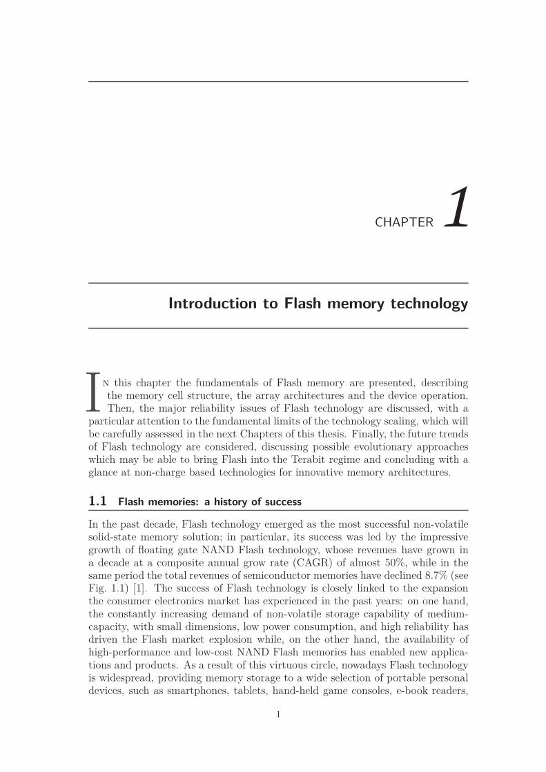
In the past decade, Flash technology emerged as the most successful non-volatilesolid-state memory solution; in particular, its success was led by the impressivegrowth of floating gate NAND Flash technology, whose revenues have grown ina decade at a composite annual grow rate (CAGR) of almost 50%, while in thesame period the total revenues of semiconductor memories have declined 8.7% (seeFig. 1.1) [1]. The success of Flash technology is closely linked to the expansionthe consumer electronics market has experienced in the past years: on one hand,the constantly increasing demand of non-volatile storage capability of medium-capacity, with small dimensions, low power consumption, and high reliability hasdriven the Flash market explosion while, on the other hand, the availability ofhigh-performance and low-cost NAND Flash memories has enabled new applica-tions and products. As a result of this virtuous circle, nowadays Flash technologyis widespread, providing memory storage to a wide selection of portable personaldevices, such as smartphones, tablets, hand-held game consoles, e-book readers,
1
Chapter 1. Introduction to Flash memory technology
Figure 1.1: Last decade semiconductor memory market (source: WSTS, Forward Insight,from [1]).
(a) (b)
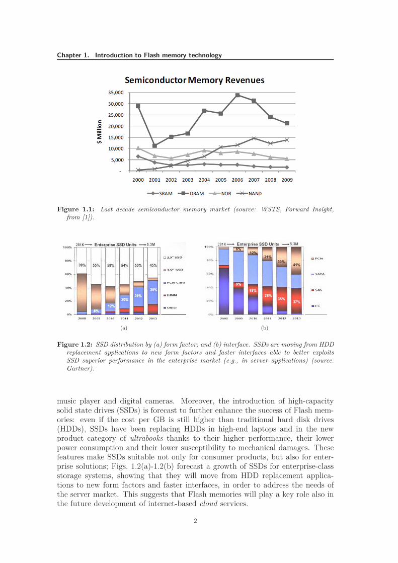
Figure 1.2: SSD distribution by (a) form factor; and (b) interface. SSDs are moving from HDDreplacement applications to new form factors and faster interfaces able to better exploitsSSD superior performance in the enterprise market (e.g., in server applications) (source:Gartner).
music player and digital cameras. Moreover, the introduction of high-capacitysolid state drives (SSDs) is forecast to further enhance the success of Flash mem-ories: even if the cost per GB is still higher than traditional hard disk drives(HDDs), SSDs have been replacing HDDs in high-end laptops and in the newproduct category of ultrabooks thanks to their higher performance, their lowerpower consumption and their lower susceptibility to mechanical damages. Thesefeatures make SSDs suitable not only for consumer products, but also for enter-prise solutions; Figs. 1.2(a)-1.2(b) forecast a growth of SSDs for enterprise-classstorage systems, showing that they will move from HDD replacement applica-tions to new form factors and faster interfaces, in order to address the needs ofthe server market. This suggests that Flash memories will play a key role also inthe future development of internet-based cloud services.
2
1.1. Flash memories: a history of success
1985 1989 1993 1997 2001 2005 2009 2013Year
10
100
1000T
ech.
nod
e [n
m]
Historical trendLast 5 years
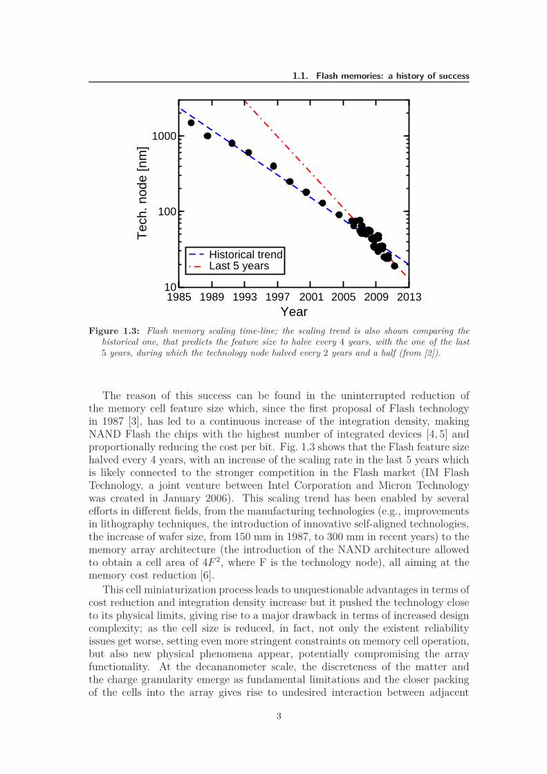
Figure 1.3: Flash memory scaling time-line; the scaling trend is also shown comparing thehistorical one, that predicts the feature size to halve every 4 years, with the one of the last5 years, during which the technology node halved every 2 years and a half (from [2]).
The reason of this success can be found in the uninterrupted reduction ofthe memory cell feature size which, since the first proposal of Flash technologyin 1987 [3], has led to a continuous increase of the integration density, makingNAND Flash the chips with the highest number of integrated devices [4, 5] andproportionally reducing the cost per bit. Fig. 1.3 shows that the Flash feature sizehalved every 4 years, with an increase of the scaling rate in the last 5 years whichis likely connected to the stronger competition in the Flash market (IM FlashTechnology, a joint venture between Intel Corporation and Micron Technologywas created in January 2006). This scaling trend has been enabled by severalefforts in different fields, from the manufacturing technologies (e.g., improvementsin lithography techniques, the introduction of innovative self-aligned technologies,the increase of wafer size, from 150 mm in 1987, to 300 mm in recent years) to thememory array architecture (the introduction of the NAND architecture allowedto obtain a cell area of 4F 2, where F is the technology node), all aiming at thememory cost reduction [6].
This cell miniaturization process leads to unquestionable advantages in terms ofcost reduction and integration density increase but it pushed the technology closeto its physical limits, giving rise to a major drawback in terms of increased designcomplexity; as the cell size is reduced, in fact, not only the existent reliabilityissues get worse, setting even more stringent constraints on memory cell operation,but also new physical phenomena appear, potentially compromising the arrayfunctionality. At the decananometer scale, the discreteness of the matter andthe charge granularity emerge as fundamental limitations and the closer packingof the cells into the array gives rise to undesired interaction between adjacent
3
Chapter 1. Introduction to Flash memory technology
(a) (b)
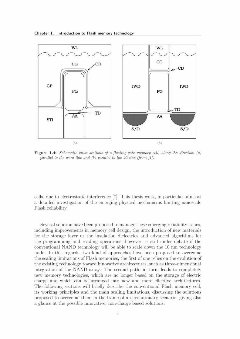
Figure 1.4: Schematic cross sections of a floating-gate memory cell, along the direction (a)parallel to the word line and (b) parallel to the bit line (from [1]).
cells, due to electrostatic interference [7]. This thesis work, in particular, aims ata detailed investigation of the emerging physical mechanisms limiting nanoscaleFlash reliability.
Several solution have been proposed to manage these emerging reliability issues,including improvements in memory cell design, the introduction of new materialsfor the storage layer or the insulation dielectrics and advanced algorithms forthe programming and reading operations; however, it still under debate if theconventional NAND technology will be able to scale down the 10 nm technologynode. In this regards, two kind of approaches have been proposed to overcomethe scaling limitations of Flash memories, the first of one relies on the evolution ofthe existing technology toward innovative architectures, such as three-dimensionalintegration of the NAND array. The second path, in turn, leads to completelynew memory technologies, which are no longer based on the storage of electriccharge and which can be arranged into new and more effective architectures.The following sections will briefly describe the conventional Flash memory cell,its working principles and the main scaling limitations, discussing the solutionsproposed to overcome them in the frame of an evolutionary scenario, giving alsoa glance at the possible innovative, non-charge based solutions.
4
1.2. Flash Technology
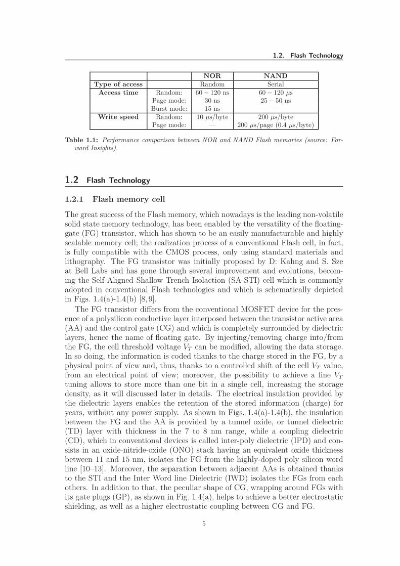
NOR NAND
Type of access Random SerialAccess time Random: 60 − 120 ns 60 − 120 µs
Page mode: 30 ns 25 − 50 nsBurst mode: 15 ns —
Write speed Random: 10 µs/byte 200 µs/bytePage mode: — 200 µs/page (0.4 µs/byte)
Table 1.1: Performance comparison between NOR and NAND Flash memories (source: For-ward Insights).
1.2 Flash Technology
1.2.1 Flash memory cell
The great success of the Flash memory, which nowadays is the leading non-volatilesolid state memory technology, has been enabled by the versatility of the floating-gate (FG) transistor, which has shown to be an easily manufacturable and highlyscalable memory cell; the realization process of a conventional Flash cell, in fact,is fully compatible with the CMOS process, only using standard materials andlithography. The FG transistor was initially proposed by D: Kahng and S. Szeat Bell Labs and has gone through several improvement and evolutions, becom-ing the Self-Aligned Shallow Trench Isolaction (SA-STI) cell which is commonlyadopted in conventional Flash technologies and which is schematically depictedin Figs. 1.4(a)-1.4(b) [8, 9].
The FG transistor differs from the conventional MOSFET device for the pres-ence of a polysilicon conductive layer interposed between the transistor active area(AA) and the control gate (CG) and which is completely surrounded by dielectriclayers, hence the name of floating gate. By injecting/removing charge into/fromthe FG, the cell threshold voltage VT can be modified, allowing the data storage.In so doing, the information is coded thanks to the charge stored in the FG, by aphysical point of view and, thus, thanks to a controlled shift of the cell VT value,from an electrical point of view; moreover, the possibility to achieve a fine VT
tuning allows to store more than one bit in a single cell, increasing the storagedensity, as it will discussed later in details. The electrical insulation provided bythe dielectric layers enables the retention of the stored information (charge) foryears, without any power supply. As shown in Figs. 1.4(a)-1.4(b), the insulationbetween the FG and the AA is provided by a tunnel oxide, or tunnel dielectric(TD) layer with thickness in the 7 to 8 nm range, while a coupling dielectric(CD), which in conventional devices is called inter-poly dielectric (IPD) and con-sists in an oxide-nitride-oxide (ONO) stack having an equivalent oxide thicknessbetween 11 and 15 nm, isolates the FG from the highly-doped poly silicon wordline [10–13]. Moreover, the separation between adjacent AAs is obtained thanksto the STI and the Inter Word line Dielectric (IWD) isolates the FGs from eachothers. In addition to that, the peculiar shape of CG, wrapping around FGs withits gate plugs (GP), as shown in Fig. 1.4(a), helps to achieve a better electrostaticshielding, as well as a higher electrostatic coupling between CG and FG.
5
Chapter 1. Introduction to Flash memory technology
Bit Line
WordLine
LineSource
(a)
SourceLine
Ground SelectLine
String SelectLine
WordLine
Bit Line
(b)
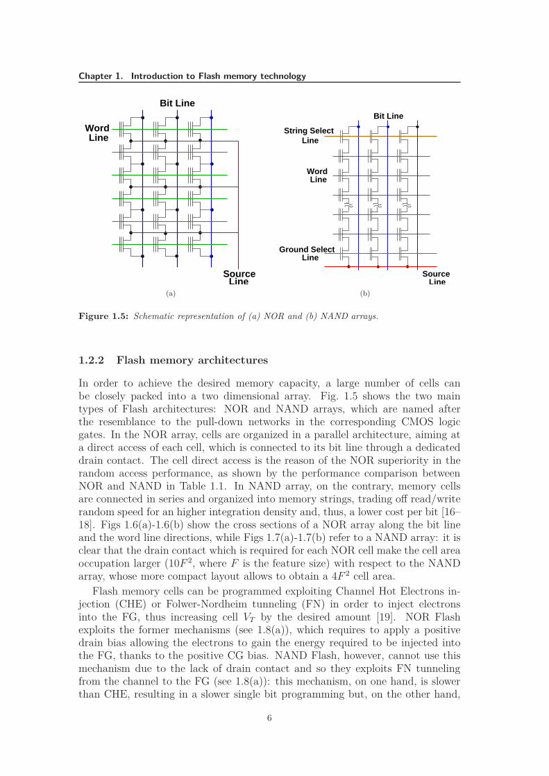
Figure 1.5: Schematic representation of (a) NOR and (b) NAND arrays.
1.2.2 Flash memory architectures
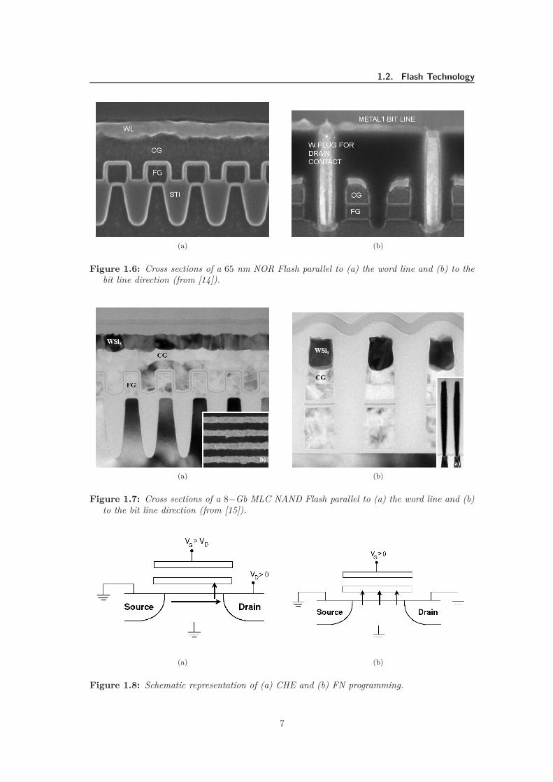
In order to achieve the desired memory capacity, a large number of cells canbe closely packed into a two dimensional array. Fig. 1.5 shows the two maintypes of Flash architectures: NOR and NAND arrays, which are named afterthe resemblance to the pull-down networks in the corresponding CMOS logicgates. In the NOR array, cells are organized in a parallel architecture, aiming ata direct access of each cell, which is connected to its bit line through a dedicateddrain contact. The cell direct access is the reason of the NOR superiority in therandom access performance, as shown by the performance comparison betweenNOR and NAND in Table 1.1. In NAND array, on the contrary, memory cellsare connected in series and organized into memory strings, trading off read/writerandom speed for an higher integration density and, thus, a lower cost per bit [16–18]. Figs 1.6(a)-1.6(b) show the cross sections of a NOR array along the bit lineand the word line directions, while Figs 1.7(a)-1.7(b) refer to a NAND array: it isclear that the drain contact which is required for each NOR cell make the cell areaoccupation larger (10F 2, where F is the feature size) with respect to the NANDarray, whose more compact layout allows to obtain a 4F 2 cell area.
Flash memory cells can be programmed exploiting Channel Hot Electrons in-jection (CHE) or Folwer-Nordheim tunneling (FN) in order to inject electronsinto the FG, thus increasing cell VT by the desired amount [19]. NOR Flashexploits the former mechanisms (see 1.8(a)), which requires to apply a positivedrain bias allowing the electrons to gain the energy required to be injected intothe FG, thanks to the positive CG bias. NAND Flash, however, cannot use thismechanism due to the lack of drain contact and so they exploits FN tunnelingfrom the channel to the FG (see 1.8(a)): this mechanism, on one hand, is slowerthan CHE, resulting in a slower single bit programming but, on the other hand,
6
1.2. Flash Technology
(a) (b)
Figure 1.6: Cross sections of a 65 nm NOR Flash parallel to (a) the word line and (b) to thebit line direction (from [14]).
(a) (b)
Figure 1.7: Cross sections of a 8−Gb MLC NAND Flash parallel to (a) the word line and (b)to the bit line direction (from [15]).
(a) (b)
Figure 1.8: Schematic representation of (a) CHE and (b) FN programming.
7
Chapter 1. Introduction to Flash memory technology
(a) (b)
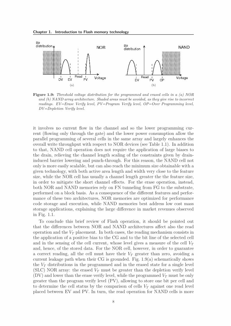
Figure 1.9: Threshold voltage distribution for the programmed and erased cells in a (a) NORand (b) NAND array architecture. Shaded areas must be avoided, as they give rise to incorrectreadings. EV=Erase Verify level, PV=Program Verify level, OP=Over Programming level,DV=Depletion Verify level.
it involves no current flow in the channel and so the lower programming cur-rent (flowing only through the gate) and the lower power consumption allow theparallel programming of several cells in the same array and largely enhances theoverall write throughput with respect to NOR devices (see Table 1.1). In additionto that, NAND cell operation does not require the application of large biases tothe drain, relieving the channel length scaling of the constraints given by drain-induced barrier lowering and punch-through. For this reason, the NAND cell notonly is more easily scalable, but can also reach the minimum size obtainable with agiven technology, with both active area length and width very close to the featuresize, while the NOR cell has usually a channel length greater the the feature size,in order to mitigate the short channel effects. For the erase operation, instead,both NOR and NAND memories rely on FN tunneling from FG to the substrate,performed on a block basis. As a consequence of the different features and perfor-mance of these two architectures, NOR memories are optimized for performancecode storage and execution, while NAND memories best address low cost massstorage applications, explaining the large difference in market revenues observedin Fig. 1.1.
To conclude this brief review of Flash operation, it should be pointed outthat the differences between NOR and NAND architectures affect also the readoperation and the VT placement. In both cases, the reading mechanism consists inthe application of a positive bias to the CG and to the bit line of the selected celland in the sensing of the cell current, whose level gives a measure of the cell VT
and, hence, of the stored data. For the NOR cell, however, in order to guaranteea correct reading, all the cell must have their VT greater than zero, avoiding acurrent leakage path when their CG is grounded. Fig. 1.9(a) schematically showsthe VT distributions in the programmed and in the erased state for a single level(SLC) NOR array: the erased VT must be greater than the depletion verify level(DV) and lower than the erase verify level, while the programmed VT must be onlygreater than the program verify level (PV), allowing to store one bit per cell andto determine the cell status by the comparison of cells VT against one read levelplaced between EV and PV. In turn, the read operation for NAND cells is more
8
1.3. Reliability constraints to Flash operation
(a) (b)
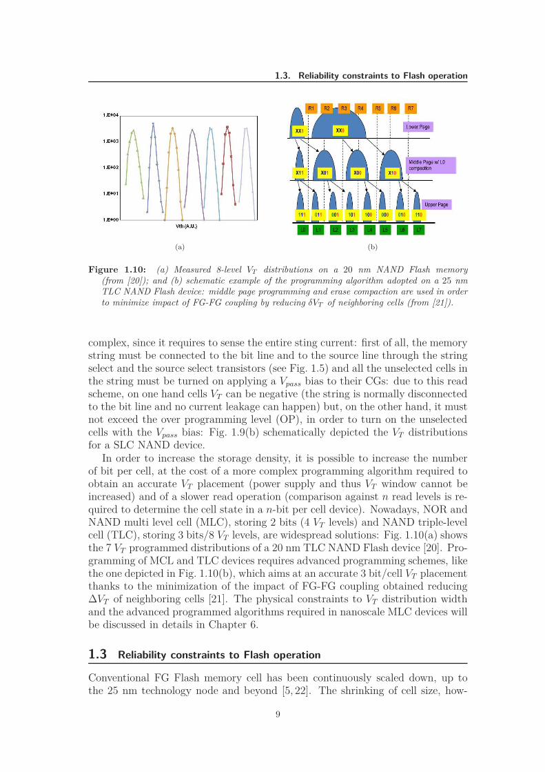
Figure 1.10: (a) Measured 8-level VT distributions on a 20 nm NAND Flash memory(from [20]); and (b) schematic example of the programming algorithm adopted on a 25 nmTLC NAND Flash device: middle page programming and erase compaction are used in orderto minimize impact of FG-FG coupling by reducing δVT of neighboring cells (from [21]).
complex, since it requires to sense the entire sting current: first of all, the memorystring must be connected to the bit line and to the source line through the stringselect and the source select transistors (see Fig. 1.5) and all the unselected cells inthe string must be turned on applying a Vpass bias to their CGs: due to this readscheme, on one hand cells VT can be negative (the string is normally disconnectedto the bit line and no current leakage can happen) but, on the other hand, it mustnot exceed the over programming level (OP), in order to turn on the unselectedcells with the Vpass bias: Fig. 1.9(b) schematically depicted the VT distributionsfor a SLC NAND device.
In order to increase the storage density, it is possible to increase the numberof bit per cell, at the cost of a more complex programming algorithm required toobtain an accurate VT placement (power supply and thus VT window cannot beincreased) and of a slower read operation (comparison against n read levels is re-quired to determine the cell state in a n-bit per cell device). Nowadays, NOR andNAND multi level cell (MLC), storing 2 bits (4 VT levels) and NAND triple-levelcell (TLC), storing 3 bits/8 VT levels, are widespread solutions: Fig. 1.10(a) showsthe 7 VT programmed distributions of a 20 nm TLC NAND Flash device [20]. Pro-gramming of MCL and TLC devices requires advanced programming schemes, likethe one depicted in Fig. 1.10(b), which aims at an accurate 3 bit/cell VT placementthanks to the minimization of the impact of FG-FG coupling obtained reducing∆VT of neighboring cells [21]. The physical constraints to VT distribution widthand the advanced programmed algorithms required in nanoscale MLC devices willbe discussed in details in Chapter 6.
1.3 Reliability constraints to Flash operation
Conventional FG Flash memory cell has been continuously scaled down, up tothe 25 nm technology node and beyond [5, 22]. The shrinking of cell size, how-
9
Chapter 1. Introduction to Flash memory technology
(a) (b)
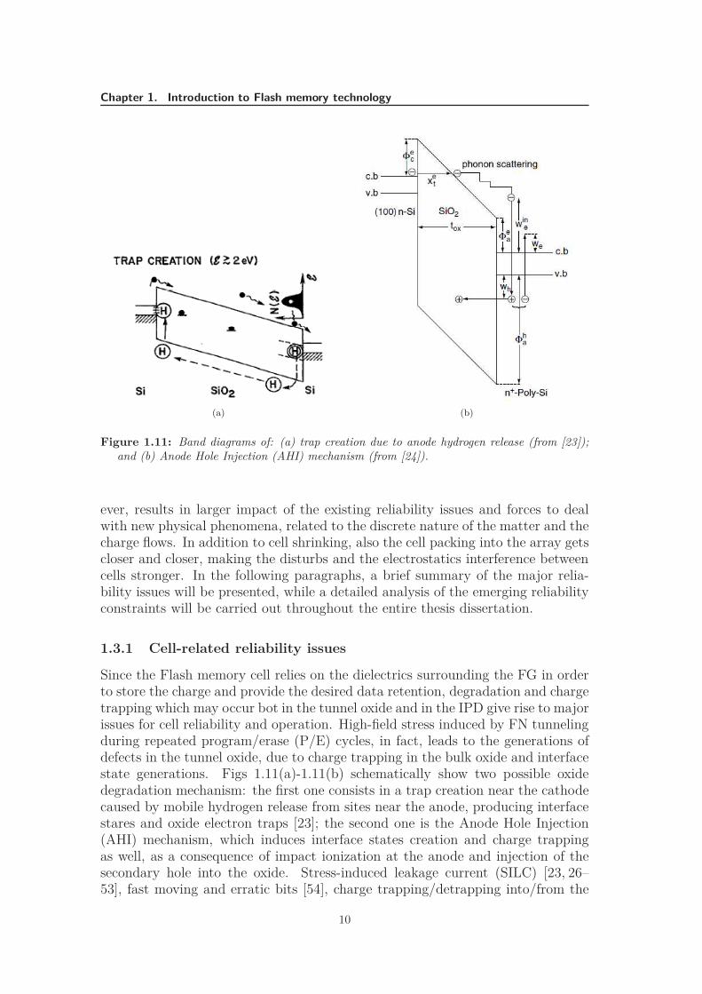
Figure 1.11: Band diagrams of: (a) trap creation due to anode hydrogen release (from [23]);and (b) Anode Hole Injection (AHI) mechanism (from [24]).
ever, results in larger impact of the existing reliability issues and forces to dealwith new physical phenomena, related to the discrete nature of the matter and thecharge flows. In addition to cell shrinking, also the cell packing into the array getscloser and closer, making the disturbs and the electrostatics interference betweencells stronger. In the following paragraphs, a brief summary of the major relia-bility issues will be presented, while a detailed analysis of the emerging reliabilityconstraints will be carried out throughout the entire thesis dissertation.
1.3.1 Cell-related reliability issues
Since the Flash memory cell relies on the dielectrics surrounding the FG in orderto store the charge and provide the desired data retention, degradation and chargetrapping which may occur bot in the tunnel oxide and in the IPD give rise to majorissues for cell reliability and operation. High-field stress induced by FN tunnelingduring repeated program/erase (P/E) cycles, in fact, leads to the generations ofdefects in the tunnel oxide, due to charge trapping in the bulk oxide and interfacestate generations. Figs 1.11(a)-1.11(b) schematically show two possible oxidedegradation mechanism: the first one consists in a trap creation near the cathodecaused by mobile hydrogen release from sites near the anode, producing interfacestares and oxide electron traps [23]; the second one is the Anode Hole Injection(AHI) mechanism, which induces interface states creation and charge trappingas well, as a consequence of impact ionization at the anode and injection of thesecondary hole into the oxide. Stress-induced leakage current (SILC) [23, 26–53], fast moving and erratic bits [54], charge trapping/detrapping into/from the
10
1.3. Reliability constraints to Flash operation
(a) (b)
Figure 1.12: (a) Cumulative VT distributions during an accelerated retention test with a nega-tive bias applied at CG (from [25]); and (b) schematic representation of the 2TAT mechanism(from [26]).
gate dielectrics and interface state generation/annealing [55–67], are well-knownreliability issues for NAND Flash memories, related to oxide degradation andcharge trapping phenomena.
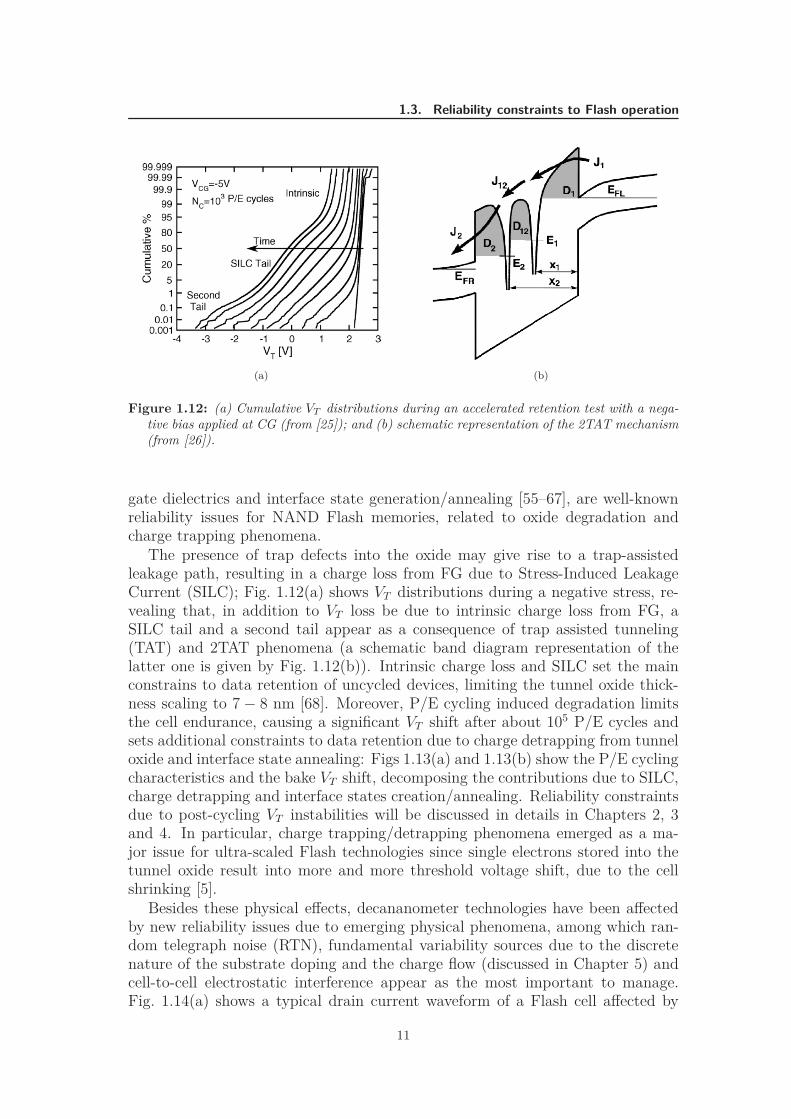
The presence of trap defects into the oxide may give rise to a trap-assistedleakage path, resulting in a charge loss from FG due to Stress-Induced LeakageCurrent (SILC); Fig. 1.12(a) shows VT distributions during a negative stress, re-vealing that, in addition to VT loss be due to intrinsic charge loss from FG, aSILC tail and a second tail appear as a consequence of trap assisted tunneling(TAT) and 2TAT phenomena (a schematic band diagram representation of thelatter one is given by Fig. 1.12(b)). Intrinsic charge loss and SILC set the mainconstrains to data retention of uncycled devices, limiting the tunnel oxide thick-ness scaling to 7 − 8 nm [68]. Moreover, P/E cycling induced degradation limitsthe cell endurance, causing a significant VT shift after about 105 P/E cycles andsets additional constraints to data retention due to charge detrapping from tunneloxide and interface state annealing: Figs 1.13(a) and 1.13(b) show the P/E cyclingcharacteristics and the bake VT shift, decomposing the contributions due to SILC,charge detrapping and interface states creation/annealing. Reliability constraintsdue to post-cycling VT instabilities will be discussed in details in Chapters 2, 3and 4. In particular, charge trapping/detrapping phenomena emerged as a ma-jor issue for ultra-scaled Flash technologies since single electrons stored into thetunnel oxide result into more and more threshold voltage shift, due to the cellshrinking [5].
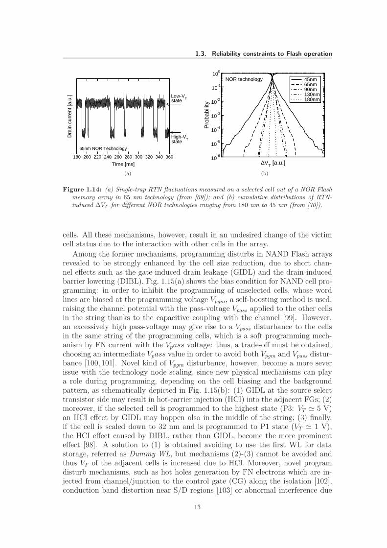
Besides these physical effects, decananometer technologies have been affectedby new reliability issues due to emerging physical phenomena, among which ran-dom telegraph noise (RTN), fundamental variability sources due to the discretenature of the substrate doping and the charge flow (discussed in Chapter 5) andcell-to-cell electrostatic interference appear as the most important to manage.Fig. 1.14(a) shows a typical drain current waveform of a Flash cell affected by
11
Chapter 1. Introduction to Flash memory technology
(a) (b)
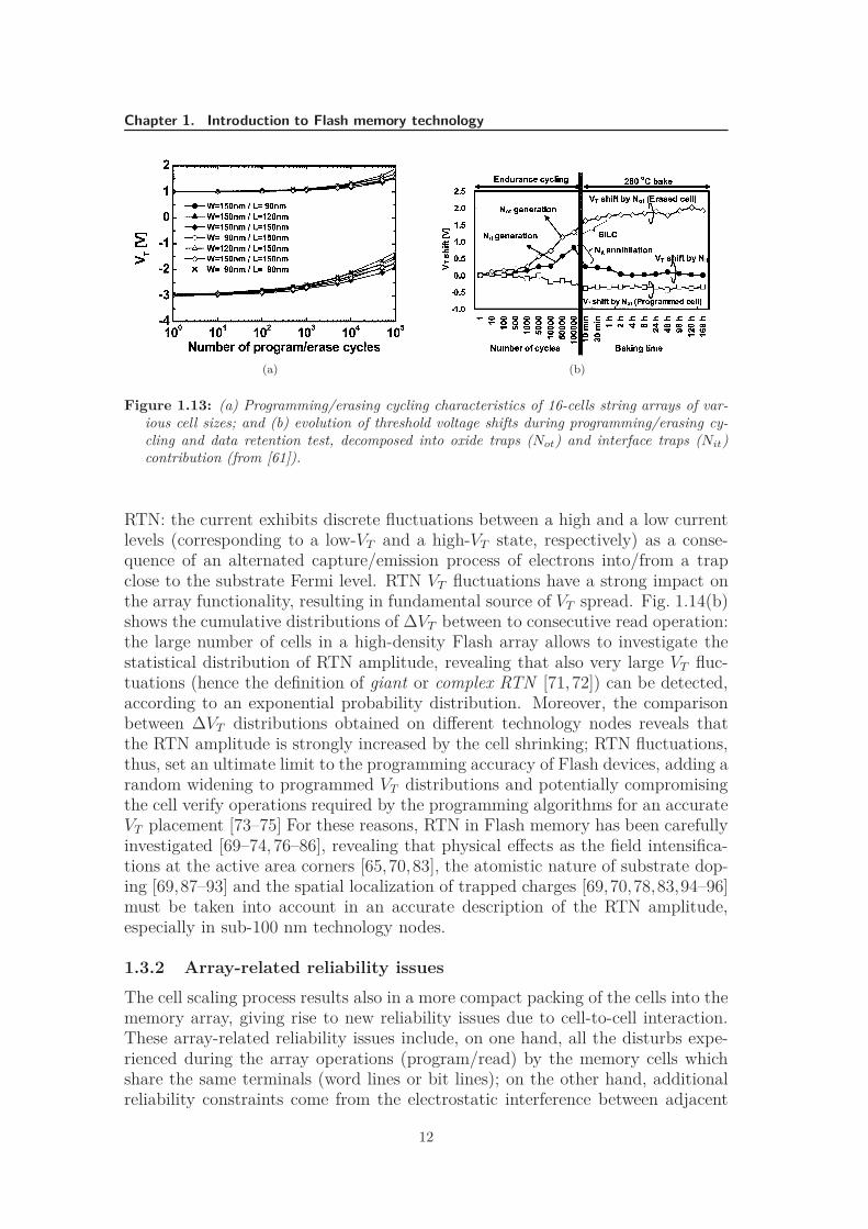
Figure 1.13: (a) Programming/erasing cycling characteristics of 16-cells string arrays of var-ious cell sizes; and (b) evolution of threshold voltage shifts during programming/erasing cy-cling and data retention test, decomposed into oxide traps (Not) and interface traps (Nit)contribution (from [61]).
RTN: the current exhibits discrete fluctuations between a high and a low currentlevels (corresponding to a low-VT and a high-VT state, respectively) as a conse-quence of an alternated capture/emission process of electrons into/from a trapclose to the substrate Fermi level. RTN VT fluctuations have a strong impact onthe array functionality, resulting in fundamental source of VT spread. Fig. 1.14(b)shows the cumulative distributions of ∆VT between to consecutive read operation:the large number of cells in a high-density Flash array allows to investigate thestatistical distribution of RTN amplitude, revealing that also very large VT fluc-tuations (hence the definition of giant or complex RTN [71, 72]) can be detected,according to an exponential probability distribution. Moreover, the comparisonbetween ∆VT distributions obtained on different technology nodes reveals thatthe RTN amplitude is strongly increased by the cell shrinking; RTN fluctuations,thus, set an ultimate limit to the programming accuracy of Flash devices, adding arandom widening to programmed VT distributions and potentially compromisingthe cell verify operations required by the programming algorithms for an accurateVT placement [73–75] For these reasons, RTN in Flash memory has been carefullyinvestigated [69–74, 76–86], revealing that physical effects as the field intensifica-tions at the active area corners [65,70,83], the atomistic nature of substrate dop-ing [69,87–93] and the spatial localization of trapped charges [69,70,78,83,94–96]must be taken into account in an accurate description of the RTN amplitude,especially in sub-100 nm technology nodes.
1.3.2 Array-related reliability issues
The cell scaling process results also in a more compact packing of the cells into thememory array, giving rise to new reliability issues due to cell-to-cell interaction.These array-related reliability issues include, on one hand, all the disturbs expe-rienced during the array operations (program/read) by the memory cells whichshare the same terminals (word lines or bit lines); on the other hand, additionalreliability constraints come from the electrostatic interference between adjacent
12
1.3. Reliability constraints to Flash operation
180 200 220 240 260 280 300 320 340 360
Time [ms]
Dra
in c
urre
nt [a
.u.]
stateLow-VT
High-VTstate65nm NOR Technology
(a)
∆VT [a.u.]10
-6
10-5
10-4
10-3
10-2
10-1
100
Pro
babi
lity
45nm65nm90nm130nm180nm
NOR technology
(b)
Figure 1.14: (a) Single-trap RTN fluctuations measured on a selected cell out of a NOR Flashmemory array in 65 nm technology (from [69]); and (b) cumulative distributions of RTN-induced ∆VT for different NOR technologies ranging from 180 nm to 45 nm (from [70]).
cells. All these mechanisms, however, result in an undesired change of the victimcell status due to the interaction with other cells in the array.
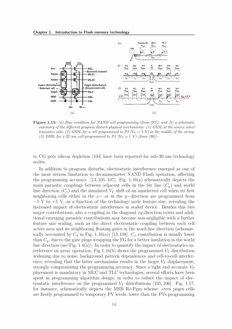
Among the former mechanisms, programming disturbs in NAND Flash arraysrevealed to be strongly enhanced by the cell size reduction, due to short chan-nel effects such as the gate-induced drain leakage (GIDL) and the drain-inducedbarrier lowering (DIBL). Fig. 1.15(a) shows the bias condition for NAND cell pro-gramming: in order to inhibit the programming of unselected cells, whose wordlines are biased at the programming voltage Vpgm, a self-boosting method is used,raising the channel potential with the pass-voltage Vpass applied to the other cellsin the string thanks to the capacitive coupling with the channel [99]. However,an excessively high pass-voltage may give rise to a Vpass disturbance to the cellsin the same string of the programming cells, which is a soft programming mech-anism by FN current with the Vpass voltage: thus, a trade-off must be obtained,choosing an intermediate Vpass value in order to avoid both Vpgm and Vpass distur-bance [100, 101]. Novel kind of Vpgm disturbance, however, become a more severissue with the technology node scaling, since new physical mechanisms can playa role during programming, depending on the cell biasing and the backgroundpattern, as schematically depicted in Fig. 1.15(b): (1) GIDL at the source selecttransistor side may result in hot-carrier injection (HCI) into the adjacent FGs; (2)moreover, if the selected cell is programmed to the highest state (P3: VT ≃ 5 V)an HCI effect by GIDL may happen also in the middle of the string; (3) finally,if the cell is scaled down to 32 nm and is programmed to P1 state (VT ≃ 1 V),the HCI effect caused by DIBL, rather than GIDL, become the more prominenteffect [98]. A solution to (1) is obtained avoiding to use the first WL for datastorage, referred as Dummy WL, but mechanisms (2)-(3) cannot be avoided andthus VT of the adjacent cells is increased due to HCI. Moreover, novel programdisturb mechanisms, such as hot holes generation by FN electrons which are in-jected from channel/junction to the control gate (CG) along the isolation [102],conduction band distortion near S/D regions [103] or abnormal interference due
13
Chapter 1. Introduction to Flash memory technology
(a) (b)
Figure 1.15: (a) Bias condition for NAND cell programming (from [97]); and (b) a schematicsummary of the different program disturb physical mechanisms: (1) GIDL at the source selecttransistor side; (2) GIDL for a cell programmed to P3 (VT ≃ 5 V) in the middle of the string;(3) DIBL for a 32 nm cell programmed to P1 (VT ≃ 1 V) (from [98]).
to CG poly silicon depletion [104] have been reported for sub-30 nm technologynodes.
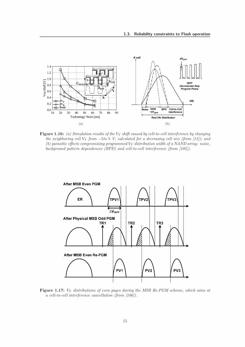
In addition to program disturbs, electrostatic interference emerged as one ofthe most serious limitation to decananometer NAND Flash operation, affectingthe programming accuracy [13, 105–107]. Fig. 1.16(a) schematically depicts themain parasitic couplings between adjacent cells in the bit line (Cy) and worldline direction (Cx) and the simulated VT shift of an unselected cell when its firstneighboring cells either in the x− or in the y−direction are programmed from−5 V to +5 V, as a function of the technology node feature size, revealing theincreased impact of electrostatic interference in scaled device. Besides this twomajor contributions, also a coupling in the diagonal xy-direction exists and addi-tional emerging parasitic contributions may become non-negligible with a furtherfeature size scaling, such as the direct electrostatic coupling between each cellactive area and its neighboring floating gates in the word-line direction (schemat-ically accounted by Cd in Fig. 1.16(a)) [13, 108]. Cx contribution is usually lowerthan Cy, due to the gate plugs wrapping the FG for a better insulation in the worldline direction (see Fig. 1.4(a)). In order to quantify the impact of electrostatics in-terference on array operation, Fig 1.16(b) shows the programmed VT distributionwidening due to noise, background pattern dependences and cell-to-cell interfer-ence, revealing that the latter mechanisms results in the larger VT displacement,strongly compromising the programming accuracy. Since a tight and accurate VT
placement is mandatory in MLC and TLC technologies, several efforts have beenspent in programming algorithm design, in order to reduce the impact of elec-trostatic interference on the programmed VT distributions [105, 106]. Fig. 1.17,for instance, schematically depicts the MSB Re-Pgm scheme: even pages cellsare firstly programmed to temporary PV levels, lower than the PVs programming
14
1.3. Reliability constraints to Flash operation
(a) (b)
Figure 1.16: (a) Simulation results of the VT shift caused by cell-to-cell interference by changingthe neighburing cell VT from −5to 5 V, calculated for a decreasing cell size (from [13]); and(b) parasitic effects compromising programmed VT distribution width of a NAND array: noise,background pattern dependences (BPD) and cell-to-cell interference (from [105]).
Figure 1.17: VT distributions of even pages during the MSB Re-PGM scheme, which aims ata cell-to-cell interference cancellation (from [106]).
15
Chapter 1. Introduction to Flash memory technology
(a) (b)
Figure 1.18: (a) Comparison between the cross section of (left) a 27 nm and (right) a 35 nmNAND technology by Samsung, highlighting the increase of FG aspect ratio with the nodescaling (Chipworks, [106]); and (b) cross section of the IMFT 25 nm NAND technology,showing the air gap insulation between FGs in the direction parallel to the bit line(from [5]).
algorithm aims at; then, even pages VT distributions are enlarged upward due toadjacent cells electrostatic aggression after the odd pages programming to a ran-dom multi-level pattern and, so, a re-programming of even pages cells is requiredto bring them at the desired PV levels, cancelling the impact of the cell-to-cellinterference during programming. Moreover, neighboring cells programming levelshould be considered: for this reason data randomization algorithms have beendeveloped to minimize the VT cell difference between the victim and the aggressorcells, thus reducing the interference [109]). All these solutions, however, have themain drawback of an increased algorithm complexity and a reduced programmingspeed.
1.4 Future trends for Flash technologies
1.4.1 Near the end of the roadmap?
High scalability of FG memory cell determined the widespread diffusion of Flashtechnology; however, the increasing technological complexity (e.g., the quad spacerpatterning technology required at the 1X node [22]), the previously mentioned reli-ability issues and the fundamental limitation that Flash technology is facing in thedecananometer regime, which will be extensively discussed throughout this thesis,bring into question the scalability of conventional Flash technologies beyond the10 nm node [112,113].
Among all the phenomena limiting the cell scaling, the main drawback of theFG technology appears to be its electrostatics: on one hand, a strong electrostatic
16
1.4. Future trends for Flash technologies
(a) (b)
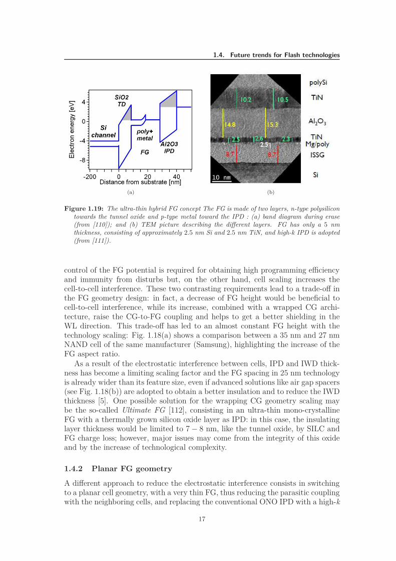
Figure 1.19: The ultra-thin hybrid FG concept The FG is made of two layers, n-type polysilicontowards the tunnel oxide and p-type metal toward the IPD : (a) band diagram during erase(from [110]); and (b) TEM picture describing the different layers. FG has only a 5 nmthickness, consisting of approximately 2.5 nm Si and 2.5 nm TiN, and high-k IPD is adopted(from [111]).
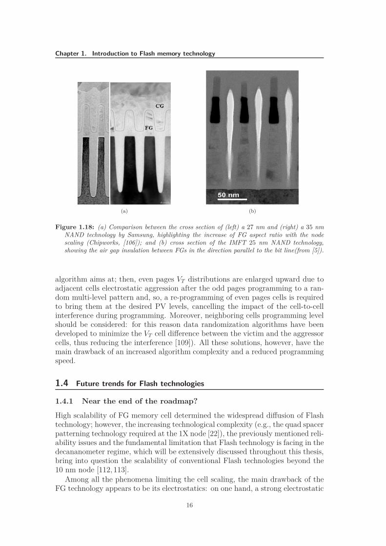
control of the FG potential is required for obtaining high programming efficiencyand immunity from disturbs but, on the other hand, cell scaling increases thecell-to-cell interference. These two contrasting requirements lead to a trade-off inthe FG geometry design: in fact, a decrease of FG height would be beneficial tocell-to-cell interference, while its increase, combined with a wrapped CG archi-tecture, raise the CG-to-FG coupling and helps to get a better shielding in theWL direction. This trade-off has led to an almost constant FG height with thetechnology scaling: Fig. 1.18(a) shows a comparison between a 35 nm and 27 nmNAND cell of the same manufacturer (Samsung), highlighting the increase of theFG aspect ratio.
As a result of the electrostatic interference between cells, IPD and IWD thick-ness has become a limiting scaling factor and the FG spacing in 25 nm technologyis already wider than its feature size, even if advanced solutions like air gap spacers(see Fig. 1.18(b)) are adopted to obtain a better insulation and to reduce the IWDthickness [5]. One possible solution for the wrapping CG geometry scaling maybe the so-called Ultimate FG [112], consisting in an ultra-thin mono-crystallineFG with a thermally grown silicon oxide layer as IPD: in this case, the insulatinglayer thickness would be limited to 7 − 8 nm, like the tunnel oxide, by SILC andFG charge loss; however, major issues may come from the integrity of this oxideand by the increase of technological complexity.
1.4.2 Planar FG geometry
A different approach to reduce the electrostatic interference consists in switchingto a planar cell geometry, with a very thin FG, thus reducing the parasitic couplingwith the neighboring cells, and replacing the conventional ONO IPD with a high-k
17
Chapter 1. Introduction to Flash memory technology
(a) (b)
Figure 1.20: Two examples of planar FG geometry: (a) IMFT 20 nm technology, with polysilicon FG and high-k IPD (source: EETimes); and (b) Macronix planar FG cell with BarrierEngineered (BE) Charge Trapping (CT) IPD (from [114]).
stack, to restore the CG-FG coupling. The main drawback of an ultra-thin FGgeometry is the gate injection through IPD, due to the lower CG-FG couplingratio leading to programming saturation and charge trapping in IPD: in order toovercome this issue, a hybrid-FG concept has been proposed in combination with alow-leakage high-k IPD: The FG is made of two layers, n-type poly silicon towardthe tunnel oxide and p-type metal toward the IPD, whose higher work functionsuppress the tunneling through IPD [111, 112]. Figs. 1.19(a)-1.19(b) shows theband structure and the gate stack of a hybrid-FG device, showing a remarkableFG thickness of only 5 nm. However, this approach may be affected by processintegration and material issues.
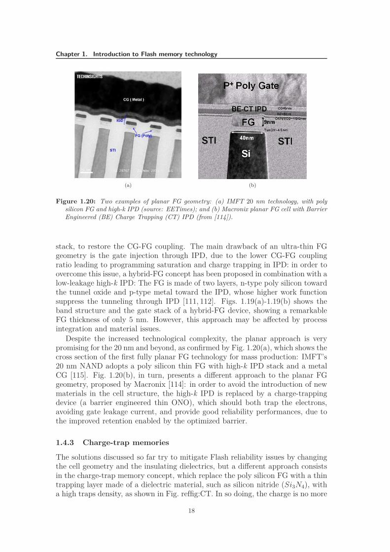
Despite the increased technological complexity, the planar approach is verypromising for the 20 nm and beyond, as confirmed by Fig. 1.20(a), which shows thecross section of the first fully planar FG technology for mass production: IMFT’s20 nm NAND adopts a poly silicon thin FG with high-k IPD stack and a metalCG [115]. Fig. 1.20(b), in turn, presents a different approach to the planar FGgeometry, proposed by Macronix [114]: in order to avoid the introduction of newmaterials in the cell structure, the high-k IPD is replaced by a charge-trappingdevice (a barrier engineered thin ONO), which should both trap the electrons,avoiding gate leakage current, and provide good reliability performances, due tothe improved retention enabled by the optimized barrier.
1.4.3 Charge-trap memories
The solutions discussed so far try to mitigate Flash reliability issues by changingthe cell geometry and the insulating dielectrics, but a different approach consistsin the charge-trap memory concept, which replace the poly silicon FG with a thintrapping layer made of a dielectric material, such as silicon nitride (Si3N4), witha high traps density, as shown in Fig. reffig:CT. In so doing, the charge is no more
18
1.4. Future trends for Flash technologies
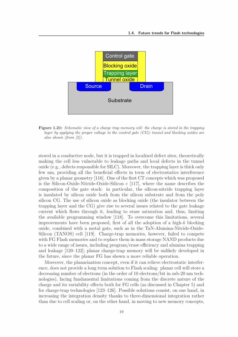
Figure 1.21: Schematic view of a charge trap memory cell: the charge is stored in the trappinglayer by applying the proper voltage to the control gate (CG); tunnel and blocking oxides arealso shown (from [2]).
stored in a conductive node, but it is trapped in localized defect sites, theoreticallymaking the cell less vulnerable to leakage paths and local defects in the tunneloxide (e.g., defects responsible for SILC). Moreover, the trapping layer is thick onlyfew nm, providing all the beneficial effects in term of electrostatics interferencegiven by a planar geometry [116]. One of the first CT concepts which was proposedis the Silicon-Oxide-Nitride-Oxide-Silicon c [117], where the name describes thecomposition of the gate stack: in particular, the silicon-nitride trapping layeris insulated by silicon oxide both from the silicon substrate and from the polysilicon CG. The use of silicon oxide as blocking oxide (the insulator between thetrapping layer and the CG) give rise to several issues related to the gate leakagecurrent which flows through it, leading to erase saturation and, thus, limitingthe available programming window [118]. To overcome this limitations, severalimprovements have been proposed, first of all the adoption of a high-k blockingoxide, combined with a metal gate, such as in the TaN-Alumina-Nitride-Oxide-Silicon (TANOS) cell [119]. Charge-trap memories, however, failed to competewith FG Flash memories and to replace them in mass storage NAND products dueto a wide range of issues, including program/erase efficiency and alumina trappingand leakage [120–122]; planar charge-trap memory will be unlikely developed inthe future, since the planar FG has shown a more reliable operation.
Moreover, the planarization concept, even if it can relieve electrostatic interfer-ence, does not provide a long term solution to Flash scaling: planar cell will store adecreasing number of electrons (in the order of 10 electrons/bit in sub-20 nm tech-nologies), facing fundamental limitations coming from the discrete nature of thecharge and its variability effects both for FG cells (as discussed in Chapter 5) andfor charge-trap technologies [123–126]. Possible solutions consist, on one hand, inincreasing the integration density thanks to three-dimensional integration ratherthan due to cell scaling or, on the other hand, in moving to new memory concepts,
19
Chapter 1. Introduction to Flash memory technology
(a) (b)
Figure 1.22: (a) The scaling-up of design rule thanks to the transition to the 3D NVM era.The inset shows the parasitic coupling as a function of design rule for planar FG cells, planarcharge-trap cells and 3D cells (from [113]); and (b) Monte Carlo simulation results showingthe programmed VT distribution width: 3D NAND geometry allow a tighter VT placement,mainly due to lower parasitic coupling.
which are not based on charge storage but rely on different physical phenomena:these approaches will be briefly discussed in the following Sections.
1.4.4 3D Flash approaches
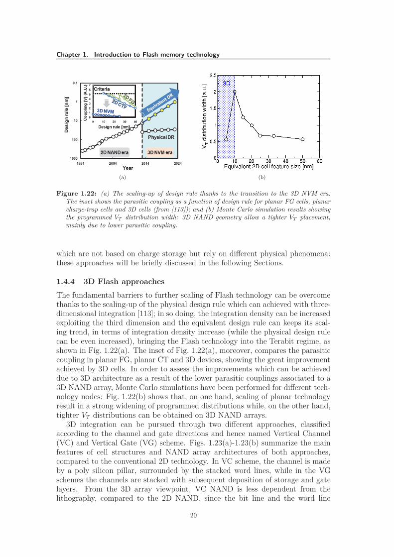
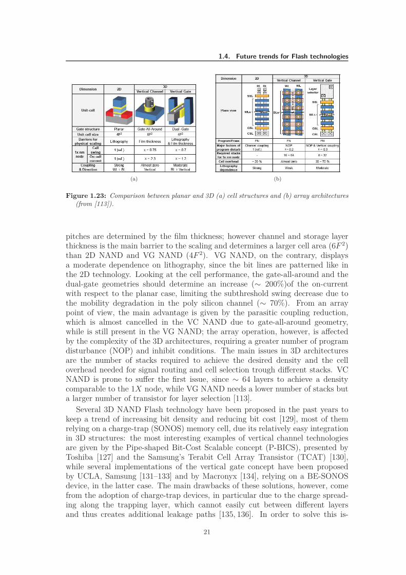
The fundamental barriers to further scaling of Flash technology can be overcomethanks to the scaling-up of the physical design rule which can achieved with three-dimensional integration [113]; in so doing, the integration density can be increasedexploiting the third dimension and the equivalent design rule can keeps its scal-ing trend, in terms of integration density increase (while the physical design rulecan be even increased), bringing the Flash technology into the Terabit regime, asshown in Fig. 1.22(a). The inset of Fig. 1.22(a), moreover, compares the parasiticcoupling in planar FG, planar CT and 3D devices, showing the great improvementachieved by 3D cells. In order to assess the improvements which can be achieveddue to 3D architecture as a result of the lower parasitic couplings associated to a3D NAND array, Monte Carlo simulations have been performed for different tech-nology nodes: Fig. 1.22(b) shows that, on one hand, scaling of planar technologyresult in a strong widening of programmed distributions while, on the other hand,tighter VT distributions can be obtained on 3D NAND arrays.
3D integration can be pursued through two different approaches, classifiedaccording to the channel and gate directions and hence named Vertical Channel(VC) and Vertical Gate (VG) scheme. Figs. 1.23(a)-1.23(b) summarize the mainfeatures of cell structures and NAND array architectures of both approaches,compared to the conventional 2D technology. In VC scheme, the channel is madeby a poly silicon pillar, surrounded by the stacked word lines, while in the VGschemes the channels are stacked with subsequent deposition of storage and gatelayers. From the 3D array viewpoint, VC NAND is less dependent from thelithography, compared to the 2D NAND, since the bit line and the word line
20
1.4. Future trends for Flash technologies
(a) (b)
Figure 1.23: Comparison between planar and 3D (a) cell structures and (b) array architectures(from [113]).
pitches are determined by the film thickness; however channel and storage layerthickness is the main barrier to the scaling and determines a larger cell area (6F 2)than 2D NAND and VG NAND (4F 2). VG NAND, on the contrary, displaysa moderate dependence on lithography, since the bit lines are patterned like inthe 2D technology. Looking at the cell performance, the gate-all-around and thedual-gate geometries should determine an increase (∼ 200%)of the on-currentwith respect to the planar case, limiting the subthreshold swing decrease due tothe mobility degradation in the poly silicon channel (∼ 70%). From an arraypoint of view, the main advantage is given by the parasitic coupling reduction,which is almost cancelled in the VC NAND due to gate-all-around geometry,while is still present in the VG NAND; the array operation, however, is affectedby the complexity of the 3D architectures, requiring a greater number of programdisturbance (NOP) and inhibit conditions. The main issues in 3D architecturesare the number of stacks required to achieve the desired density and the celloverhead needed for signal routing and cell selection trough different stacks. VCNAND is prone to suffer the first issue, since ∼ 64 layers to achieve a densitycomparable to the 1X node, while VG NAND needs a lower number of stacks buta larger number of transistor for layer selection [113].
Several 3D NAND Flash technology have been proposed in the past years tokeep a trend of increasing bit density and reducing bit cost [129], most of themrelying on a charge-trap (SONOS) memory cell, due its relatively easy integrationin 3D structures: the most interesting examples of vertical channel technologiesare given by the Pipe-shaped Bit-Cost Scalable concept (P-BICS), presented byToshiba [127] and the Samsung’s Terabit Cell Array Transistor (TCAT) [130],while several implementations of the vertical gate concept have been proposedby UCLA, Samsung [131–133] and by Macronyx [134], relying on a BE-SONOSdevice, in the latter case. The main drawbacks of these solutions, however, comefrom the adoption of charge-trap devices, in particular due to the charge spread-ing along the trapping layer, which cannot easily cut between different layersand thus creates additional leakage paths [135, 136]. In order to solve this is-
21
Chapter 1. Introduction to Flash memory technology
(a) (b)
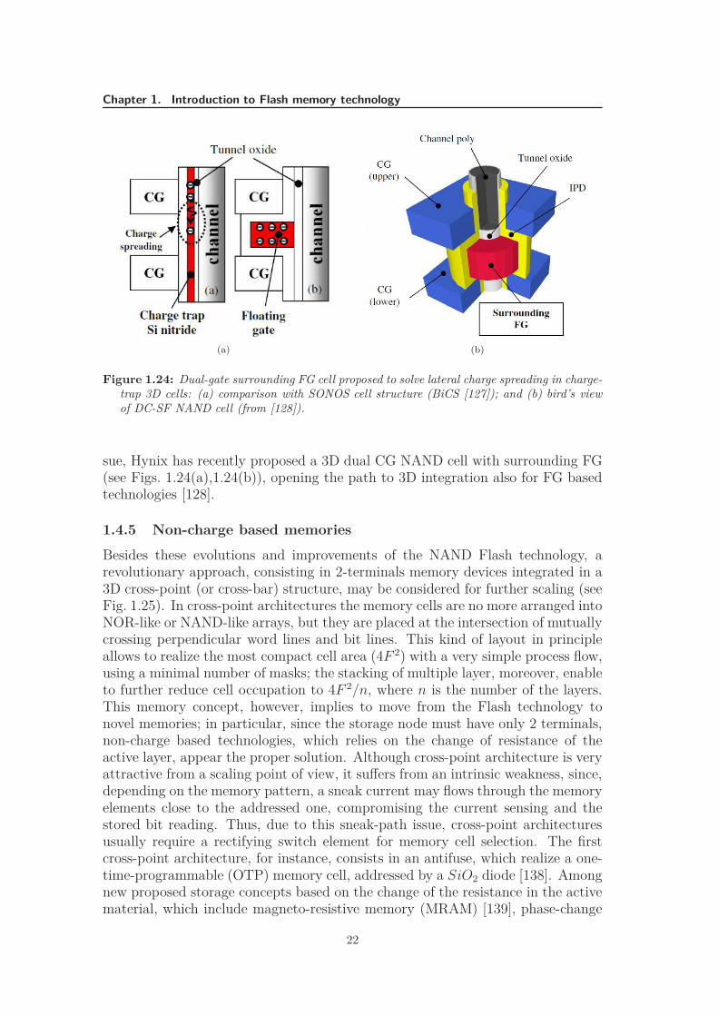
Figure 1.24: Dual-gate surrounding FG cell proposed to solve lateral charge spreading in charge-trap 3D cells: (a) comparison with SONOS cell structure (BiCS [127]); and (b) bird’s viewof DC-SF NAND cell (from [128]).
sue, Hynix has recently proposed a 3D dual CG NAND cell with surrounding FG(see Figs. 1.24(a),1.24(b)), opening the path to 3D integration also for FG basedtechnologies [128].
1.4.5 Non-charge based memories
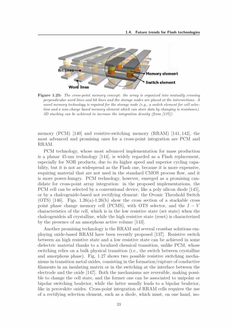
Besides these evolutions and improvements of the NAND Flash technology, arevolutionary approach, consisting in 2-terminals memory devices integrated in a3D cross-point (or cross-bar) structure, may be considered for further scaling (seeFig. 1.25). In cross-point architectures the memory cells are no more arranged intoNOR-like or NAND-like arrays, but they are placed at the intersection of mutuallycrossing perpendicular word lines and bit lines. This kind of layout in principleallows to realize the most compact cell area (4F 2) with a very simple process flow,using a minimal number of masks; the stacking of multiple layer, moreover, enableto further reduce cell occupation to 4F 2/n, where n is the number of the layers.This memory concept, however, implies to move from the Flash technology tonovel memories; in particular, since the storage node must have only 2 terminals,non-charge based technologies, which relies on the change of resistance of theactive layer, appear the proper solution. Although cross-point architecture is veryattractive from a scaling point of view, it suffers from an intrinsic weakness, since,depending on the memory pattern, a sneak current may flows through the memoryelements close to the addressed one, compromising the current sensing and thestored bit reading. Thus, due to this sneak-path issue, cross-point architecturesusually require a rectifying switch element for memory cell selection. The firstcross-point architecture, for instance, consists in an antifuse, which realize a one-time-programmable (OTP) memory cell, addressed by a SiO2 diode [138]. Amongnew proposed storage concepts based on the change of the resistance in the activematerial, which include magneto-resistive memory (MRAM) [139], phase-change
22
1.4. Future trends for Flash technologies
Figure 1.25: The cross-point memory concept: the array is organized into mutually crossingperpendicular word lines and bit lines and the storage nodes are placed at the intersections. Anovel memory technology is required for the storage node (e.g., a switch element for cell selec-tion and a non-charge based memory element which can store data by changing is resistance).3D stacking can be achieved to increase the integration density (from [137]).
memory (PCM) [140] and resistive-switching memory (RRAM) [141, 142], themost advanced and promising ones for a cross-point integration are PCM andRRAM.
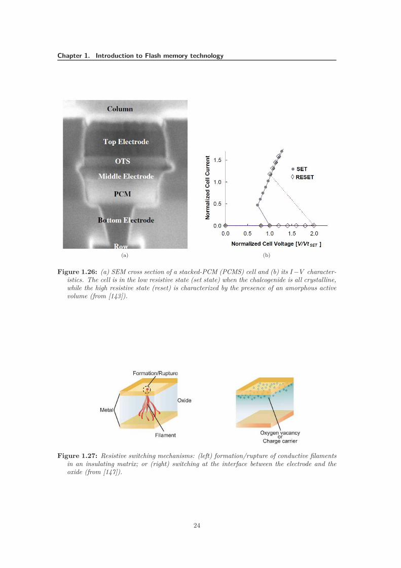
PCM technology, whose most advanced implementation for mass productionis a planar 45-nm technology [144], is widely regarded as a Flash replacement,especially for NOR products, due to its higher speed and superior cycling capa-bility, but it is not as widespread as the Flash one, because it is more expensive,requiring material that are not used in the standard CMOS process flow, and itis more power-hungry. PCM technology, however, emerged as a promising can-didate for cross-point array integration: in the proposed implementations, thePCM cell can be selected by a conventional device, like a poly silicon diode [145],or by a chalcogenide-based not rectifying element: the Ovonic Threshold Switch(OTS) [146]. Figs. 1.26(a)-1.26(b) show the cross section of a stackable crosspoint phase change memory cell (PCMS), with OTS selector, and the I − Vcharacteristics of the cell, which is in the low resistive state (set state) when thechalcogenideis all crystalline, while the high resistive state (reset) is characterizedby the presence of an amorphous active volume [143].
Another promising technology is the RRAM and several crossbar solutions em-ploying oxide-based RRAM have been recently proposed [137]. Resistive switchbetween an high resistive state and a low resistive state can be achieved in somedielectric material thanks to a localized chemical transition, unlike PCM, whoseswitching relies on a bulk physical transition (i.e., the switch between crystallineand amorphous phase). Fig. 1.27 shows two possible resistive switching mecha-nisms in transition metal oxides, consisting in the formation/rupture of conductivefilaments in an insulating matrix or in the switching at the interface between theelectrode and the oxide [147]. Both the mechanisms are reversible, making possi-ble to change the cell state, and the former one can be associated to unipolar orbipolar switching beahvior, while the latter usually leads to a bipolar beahvior,like in perovskite oxides. Cross-point integration of RRAM cells requires the useof a rectifying selection element, such as a diode, which must, on one hand, iso-
23
Chapter 1. Introduction to Flash memory technology
(a) (b)
Figure 1.26: (a) SEM cross section of a stacked-PCM (PCMS) cell and (b) its I −V character-istics. The cell is in the low resistive state (set state) when the chalcogenide is all crystalline,while the high resistive state (reset) is characterized by the presence of an amorphous activevolume (from [143]).
Figure 1.27: Resistive switching mechanisms: (left) formation/rupture of conductive filamentsin an insulating matrix; or (right) switching at the interface between the electrode and theoxide (from [147]).
24
1.5. Description of the Ph.D. research activity
late unselected cell and, on the other hand, sustain the high reset current; thesetwo requirements make the diode integration very difficult, since it must have alow leakage current, a high forward current and its size must be comparable withthe cell size. For this reason, complementary switching in metal oxides is underinvestigation, in order to obtain diode-less crossbar devices [148].
However, cross point concepts shows several practical issue to be solved andfeasibility and scaling proprieties of PCM- or RRAM-based cross point arraysshould be still assessed; even if these approaches look promising for high densityNAND replacement, floating gate Flash technology scaling and 3D integrationnowadays is regarded as the main road for he near future memory evolution.
1.5 Description of the Ph.D. research activity
The research activity is focused on the physical mechanisms limiting the reliabilityof decananometer NOR and NAND Flash memories. Firstly, the attention is fo-cused on oxide degradation and trapping/detrapping phenomena, which have beenshown to set the ultimate limits to Flash endurance and data retention: thresholdvoltage instabilities after cycling have been investigated on NAND (Chapters 2-3)and NOR arrays (Chapter 4), highlighting their dependence not only on the bakebut also on the cycling conditions, in terms of temperature and time. Exper-imental characterizations and data analyses assessed the validity of a universalmodel for damage recovery after distributed cycling, allowing the developmentof accelerated test schemes reproducing the real on-field usage of the devices.Moreover, the impact of short channel effects on string current in decananometerNAND Flash devices and the basic properties of damage creation and recovery(during cycling and bake, respectively) in nanoscale Flash devices have been alsostudied in detail in Chapter 3 thanks to a compact model for string current, pro-viding a deeper insight into the time dynamics and activation energies of chargetrapping/detrapping and interface states creation and annealing.
Then, among the emerging constraint to Flash reliability, a special interesthas been devoted to fundamental variability sources and few electron phenomena.Few electron phenomena have been considered as a source of programming noiseduring incremental step pulse programming (ISPP) of NAND arrays, studyingthe statistical dispersion of the programmed threshold voltage distribution com-ing from the granular nature of the current flow to the floating gate. The impactof floating gate and control gate doping and geometry is investigated in Chap-ter 5, addressing the scaling trend of electron injection statistics and discussingpossible cell design solution to mitigate its effects. Discrete electron emission fromthe floating gate and tunnel oxide, in fresh and cycled devices, respectively, hasbeen also considered during data retention, investigating spread contributions todata retention coming from charge granularity and cell parameters fluctuations.Moreover, using Monte Carlo numerical simulations, the possibility to increaseprogramming accuracy by means of double verify ISSP algorithms has been con-sidered in Chapter 6, highlighting benefits and drawbacks of the algorithms.
The research activity provides a clear assessment of the fundamental limita-tions of Flash technology and, more in general, of the physical mechanisms every
25

Chapter 1. Introduction to Flash memory technology
future charge-based non-volatile technology should deal with in order to delivera reliable operation. Moving from the physical understanding of the reliabilityconstraints, the thesis discusses feasible solutions in order to extend the successof Flash technology to the decananometer technology nodes and develops thetheoretical foundations of accelerated qualifications schemes for ultra-scaled tech-nologies, in order to correctly reproduce the real on field usage of the devices.
26
CHAPTER2
Cycling-Induced VT Instabilities
This chapter presents a detailed investigation of the impact of cycling timeand temperature on the threshold-voltage instability arising from damagerecovery during data retention on nanoscale NAND Flash. Statistical re-
sults from the programmed state show that instabilities result, on average, in athreshold-voltage loss which increases logarithmically with the time elapsed sincethe end of cycling. Increasing the cycling time and temperature corresponds toan equivalent delay of the instant at which the first read operation on the arrayis performed. The delay is studied for a large variety of cycling and retentionconditions, extracting the parameters required for a universal damage-recoverymetric for NAND.
2.1 Introduction
Recovey of cycling–induced damage is a major source of threshold voltage (VT )instability during data retention for deca-nanometer NAND Flash memories [60–62,65]. This instability represents the worst reliability issue coming from spuriouscharge trapping in the tunnel oxide and interface state creation during repeatedprogram/erase (P/E) cycles [55, 57, 65, 66], arising from the possibility for thesame oxide charge to detrap and for interface states to anneal out when cellshave to preserve their data [56, 58–65]. Both charge detrapping and interfacestate annealing give rise to VT displacements that are particularly critical formulti-level devices, where the higher number of bits per cell is obtained at theexpense of reduced noise margins. The statistical nature of these displacementsis well recognized [63, 64] and results from the stochastic fluctuation both of thenumber of defects per cell and of the impact of each single defect on cell VT .
27
Chapter 2. Cycling-Induced VT Instabilities
The former fluctuation is due to the very small device active area, resulting insuch a low number of defects per cell that their Poissonian dispersion cannot beneglected. The fluctuation of the impact of each single defect on cell VT is, instead,related to the possibility for the defect to be placed at different spatial positionsover the cell active area in presence of percolative substrate conduction [66, 69,75, 80, 96, 124]. Moreover, both positive and negative charges can be trappedin the tunnel oxide during cycling, giving VT shifts of opposite polarities whendetrapping takes place [57, 63]. As a result of the statistical dispersion of theVT displacements, the array VT distribution increases its spread as time elapsesduring data retention [63, 64]. In addition to that, the reliability issues comingfrom damage recovery are further worsened by the non-zero average value of thedisplacements, shifting the VT distribution along a preferential direction.
The amount of cell damage contributing to VT instabilities during data re-tention is the result not only of the number of P/E cycles previously performedon the array but also of the time delay between cycles and the cycling temper-ature [63, 64]. In fact, the possibility for partial damage recovery to take placeduring the time elapsing in between the cycles results into a lower amount ofdamage at the end of cycling when this is performed on a longer time interval.This means that lower VT instabilities during data retention are expected whenthe cycling time is increased, as clearly shown for NOR Flash memories in [63,64].As a consequence, characterization tests where P/E cycles are performed in quicksuccession to minimize the required experimental time, usually referred to as fast–
cycling tests, provide only worst case results for the VT instabilities during dataretention. A more realistic test should, instead, reproduce the time distributionof P/E cycles that is reasonably expected in real device operation. To this aim,distributed–cycling experiments should be designed, trying to solve the trade-offbetween a low characterization time and a correct reproduction of the amount ofdamage at the end of cycling. In so doing, the increase of the cycling temperatureto obtain in affordable experimental times the same damage recovery that shouldbe obtained at the device working temperature on a much longer cycling timescaleappears as the most practical solution [63, 64, 149].
This chapter presents a detailed investigation of the VT instability determinedby damage recovery during data retention on deca-nanometer NAND Flash, fo-cusing on its basic phenomenology and on its dependence on cycling time andtemperature. Extending the work we presented in [67] with more detailed discus-sions and additional results, we show that VT instabilities from the programmedstate result, on average, in a VT loss which increases logarithmically with thetime elapsed since the end of cycling. Electric field during data retention, cyclingdose and probability level at which the shift of the array cumulative distributionis monitored are all important parameters for the slope of the logarithmic VT
loss. Changes in the cycling time and temperature correspond, instead, to anequivalent delay of the instant at which the first read operation on the array isperformed. This delay is investigated for a large variety of cycling and retentionconditions, extracting the value of the parameters needed to accurately modeldistributed–cycling effects.
28
2.2. Basic phenomenology
tB
TB
VT
t*0
...
t
(b)
(a)
ReadPVP/E cycle
# of
cel
ls
PV2 PV3PV1E
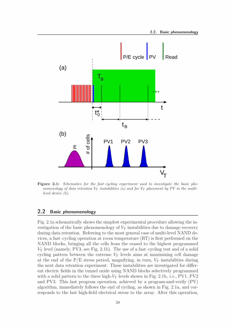
Figure 2.1: Schematics for the fast–cycling experiment used to investigate the basic phe-nomenology of data retention VT instabilities (a) and for VT placement by PV in the multi–level device (b).
2.2 Basic phenomenology
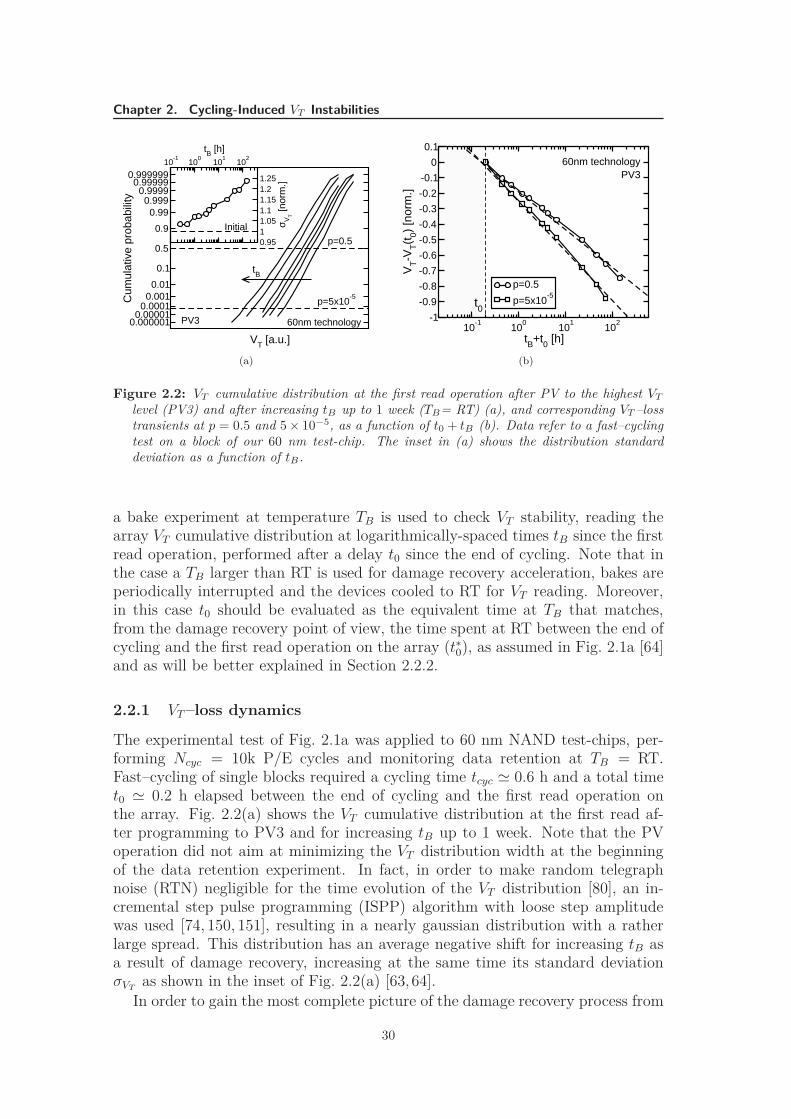
Fig. 2.1a schematically shows the simplest experimental procedure allowing the in-vestigation of the basic phenomenology of VT instabilities due to damage recoveryduring data retention. Referring to the most general case of multi-level NAND de-vices, a fast–cycling operation at room temperature (RT) is first performed on theNAND blocks, bringing all the cells from the erased to the highest programmedVT level (namely, PV3, see Fig. 2.1b). The use of a fast–cycling test and of a solidcycling pattern between the extreme VT levels aims at maximizing cell damageat the end of the P/E stress period, magnifying, in turn, VT instabilities duringthe next data retention experiment. These instabilities are investigated for differ-ent electric fields in the tunnel oxide using NAND blocks selectively programmedwith a solid pattern to the three high-VT levels shown in Fig. 2.1b, i.e., PV1, PV2and PV3. This last program operation, achieved by a program-and-verify (PV)algorithm, immediately follows the end of cycling, as shown in Fig. 2.1a, and cor-responds to the last high-field electrical stress to the array. After this operation,
29
Chapter 2. Cycling-Induced VT Instabilities
10-1
100
101
102
tB [h]
0.9511.051.11.151.21.25
σ VT [n
orm
.]
VT [a.u.]
0.000010.00010.001
0.01
0.1
0.5
0.9
0.990.999
0.99990.99999
0.000001
0.999999
Cum
ulat
ive
prob
abili
ty
p=0.5
p=5x10⁻⁵
60nm technology
tB
PV3
Initial
(a)
10-1
100
101
102
tB+t0 [h]
-1
-0.9
-0.8
-0.7
-0.6
-0.5
-0.4
-0.3
-0.2
-0.1
0
0.1
VT-V
T(t
0) [n
orm
.]
p=0.5
p=5x10⁻⁵
60nm technologyPV3
t0
(b)
Figure 2.2: VT cumulative distribution at the first read operation after PV to the highest VT
level (PV3) and after increasing tB up to 1 week (TB= RT) (a), and corresponding VT –losstransients at p = 0.5 and 5 × 10⁻⁵, as a function of t0 + tB (b). Data refer to a fast–cyclingtest on a block of our 60 nm test-chip. The inset in (a) shows the distribution standarddeviation as a function of tB.
a bake experiment at temperature TB is used to check VT stability, reading thearray VT cumulative distribution at logarithmically-spaced times tB since the firstread operation, performed after a delay t0 since the end of cycling. Note that inthe case a TB larger than RT is used for damage recovery acceleration, bakes areperiodically interrupted and the devices cooled to RT for VT reading. Moreover,in this case t0 should be evaluated as the equivalent time at TB that matches,from the damage recovery point of view, the time spent at RT between the end ofcycling and the first read operation on the array (t∗0), as assumed in Fig. 2.1a [64]and as will be better explained in Section 2.2.2.
2.2.1 VT –loss dynamics
The experimental test of Fig. 2.1a was applied to 60 nm NAND test-chips, per-forming Ncyc = 10k P/E cycles and monitoring data retention at TB = RT.Fast–cycling of single blocks required a cycling time tcyc ≃ 0.6 h and a total timet0 ≃ 0.2 h elapsed between the end of cycling and the first read operation onthe array. Fig. 2.2(a) shows the VT cumulative distribution at the first read af-ter programming to PV3 and for increasing tB up to 1 week. Note that the PVoperation did not aim at minimizing the VT distribution width at the beginningof the data retention experiment. In fact, in order to make random telegraphnoise (RTN) negligible for the time evolution of the VT distribution [80], an in-cremental step pulse programming (ISPP) algorithm with loose step amplitudewas used [74, 150, 151], resulting in a nearly gaussian distribution with a ratherlarge spread. This distribution has an average negative shift for increasing tB asa result of damage recovery, increasing at the same time its standard deviationσVT
as shown in the inset of Fig. 2.2(a) [63, 64].
In order to gain the most complete picture of the damage recovery process from
30
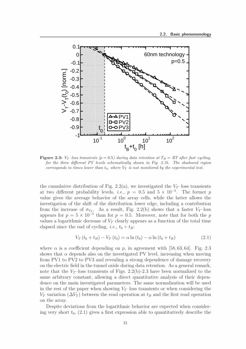
2.2. Basic phenomenology
10-1
100
101
102
tB+t0 [h]
-1
-0.9
-0.8
-0.7
-0.6
-0.5
-0.4
-0.3
-0.2
-0.1
0
0.1
VT-V
T(t
0) [n
orm
.]
PV1PV2PV3
60nm technologyp=0.5
t0
Figure 2.3: VT –loss transients (p = 0.5) during data retention at TB = RT after fast–cycling,for the three different PV levels schematically shown in Fig. 2.1b. The shadowed regioncorresponds to times lower than t0, where VT is not monitored by the experimental test.
the cumulative distribution of Fig. 2.2(a), we investigated the VT –loss transientsat two different probability levels, i.e., p = 0.5 and 5 × 10⁻⁵. The former pvalue gives the average behavior of the array cells, while the latter allows theinvestigation of the shift of the distribution lower edge, including a contributionfrom the increase of σVT
. As a result, Fig. 2.2(b) shows that a faster VT –lossappears for p = 5 × 10⁻⁵ than for p = 0.5. Moreover, note that for both the pvalues a logarithmic decrease of VT clearly appears as a function of the total timeelapsed since the end of cycling, i.e., t0 + tB:
VT (t0 + tB) − VT (t0) = α ln (t0) − α ln (t0 + tB) (2.1)
where α is a coefficient depending on p, in agreement with [58, 63, 64]. Fig. 2.3shows that α depends also on the investigated PV level, increasing when movingfrom PV1 to PV2 to PV3 and revealing a strong dependence of damage recoveryon the electric field in the tunnel oxide during data retention. As a general remark,note that the VT –loss transients of Figs. 2.2(b)-2.3 have been normalized to thesame arbitrary constant, allowing a direct quantitative analysis of their depen-dence on the main investigated parameters. The same normalization will be usedin the rest of the paper when showing VT –loss transients or when considering theVT variation (∆VT ) between the read operation at tB and the first read operationon the array.
Despite deviations from the logarithmic behavior are expected when consider-ing very short t0, (2.1) gives a first expression able to quantitatively describe the
31
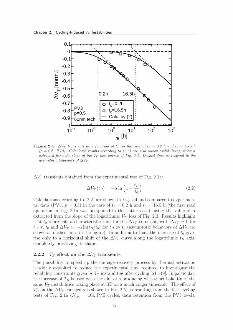
Chapter 2. Cycling-Induced VT Instabilities
10-2
10-1
100
101
102
103
tB [h]
-1
-0.9
-0.8
-0.7
-0.6
-0.5
-0.4
-0.3
-0.2
-0.1
0
0.1
∆VT [n
orm
.]
t0=0.2ht0=16.5hCalc. by (2)
PV3p=0.560nm tech.
0.2h 16.5h
Figure 2.4: ∆VT transients as a function of tB in the case of t0 = 0.2 h and t0 = 16.5 h(p = 0.5, PV3). Calculated results according to (2.2) are also shown (solid lines), using αextracted from the slope of the VT –loss curves of Fig. 2.3. Dashed lines correspond to theasymptotic behaviors of ∆VT .
∆VT transients obtained from the experimental test of Fig. 2.1a:
∆VT (tB) = −α ln(
1 +tBt0
)
(2.2)
Calculations according to (2.2) are shown in Fig. 2.4 and compared to experimen-tal data (PV3, p = 0.5) in the case of t0 = 0.2 h and t0 = 16.5 h (the first readoperation in Fig. 2.1a was postponed in this latter case), using the value of αextracted from the slope of the logarithmic VT –loss of Fig. 2.3. Results highlightthat t0 represents a characteristic time for the ∆VT transient, with ∆VT ≃ 0 fortB ≪ t0 and ∆VT ≃ −α ln(tB/t0) for tB ≫ t0 (asymptotic behaviors of ∆VT areshown as dashed lines in the figure). In addition to that, the increase of t0 givesrise only to a horizontal shift of the ∆VT curve along the logarithmic tB axis,completely preserving its shape.
2.2.2 TB effect on the ∆VT transients
The possibility to speed up the damage–recovery process by thermal activationis widely exploited to reduce the experimental time required to investigate thereliability constraints given by VT instabilities after cycling [64,149]. In particular,the increase of TB is used with the aim of reproducing with short bake times thesame VT instabilities taking place at RT on a much longer timescale. The effect ofTB on the ∆VT transients is shown in Fig. 2.5, as resulting from the fast–cyclingtests of Fig. 2.1a (Ncyc = 10k P/E cycles, data retention from the PV3 level):
32
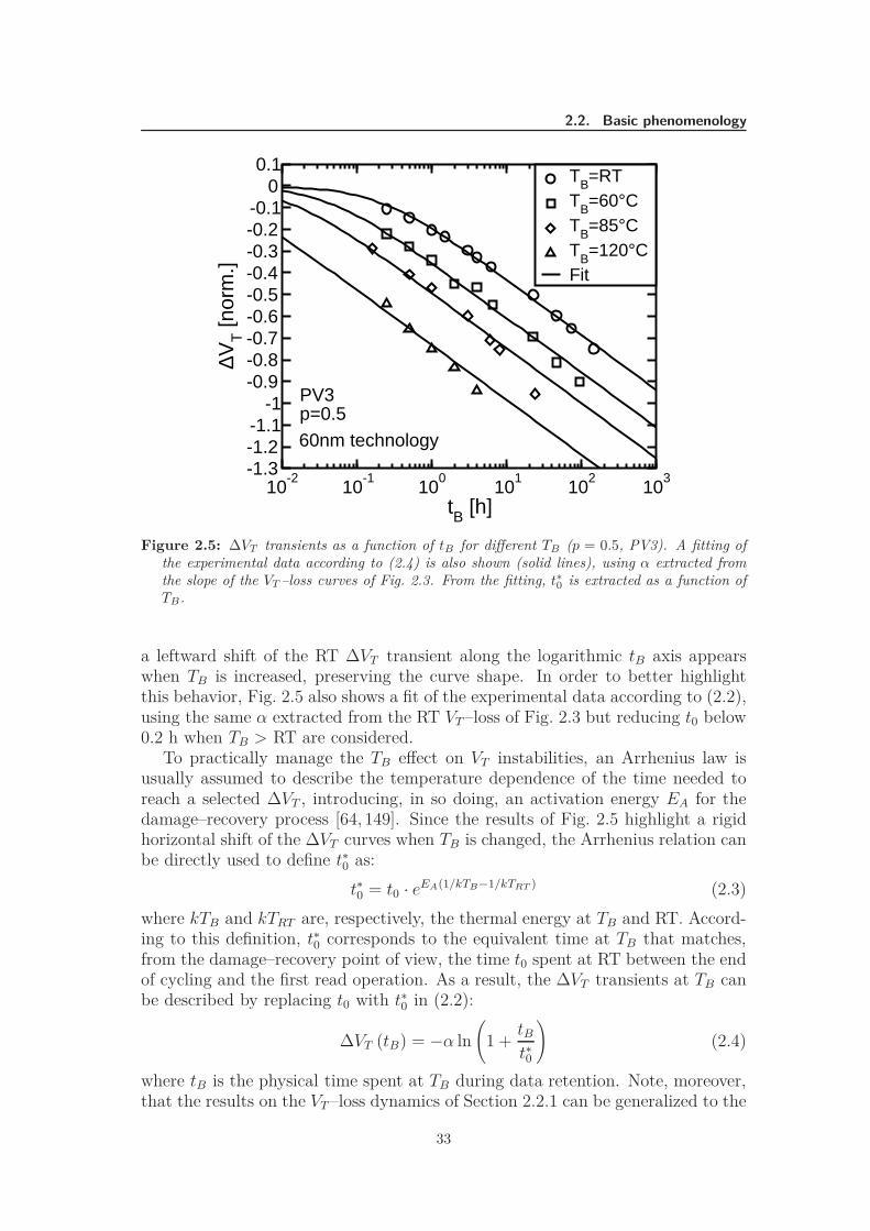
2.2. Basic phenomenology
10-2
10-1
100
101
102
103
tB [h]
-1.3-1.2-1.1
-1-0.9-0.8-0.7-0.6-0.5-0.4-0.3-0.2-0.1
00.1
∆VT [n
orm
.]
TB=RTTB=60°CTB=85°CTB=120°CFit
60nm technology
PV3p=0.5
Figure 2.5: ∆VT transients as a function of tB for different TB (p = 0.5, PV3). A fitting ofthe experimental data according to (2.4) is also shown (solid lines), using α extracted fromthe slope of the VT –loss curves of Fig. 2.3. From the fitting, t∗
0 is extracted as a function ofTB.
a leftward shift of the RT ∆VT transient along the logarithmic tB axis appearswhen TB is increased, preserving the curve shape. In order to better highlightthis behavior, Fig. 2.5 also shows a fit of the experimental data according to (2.2),using the same α extracted from the RT VT –loss of Fig. 2.3 but reducing t0 below0.2 h when TB > RT are considered.
To practically manage the TB effect on VT instabilities, an Arrhenius law isusually assumed to describe the temperature dependence of the time needed toreach a selected ∆VT , introducing, in so doing, an activation energy EA for thedamage–recovery process [64, 149]. Since the results of Fig. 2.5 highlight a rigidhorizontal shift of the ∆VT curves when TB is changed, the Arrhenius relation canbe directly used to define t∗0 as:
t∗0 = t0 · eEA(1/kTB−1/kTRT ) (2.3)
where kTB and kTRT are, respectively, the thermal energy at TB and RT. Accord-ing to this definition, t∗0 corresponds to the equivalent time at TB that matches,from the damage–recovery point of view, the time t0 spent at RT between the endof cycling and the first read operation. As a result, the ∆VT transients at TB canbe described by replacing t0 with t∗0 in (2.2):
∆VT (tB) = −α ln
(
1 +tBt∗0
)
(2.4)
where tB is the physical time spent at TB during data retention. Note, moreover,that the results on the VT –loss dynamics of Section 2.2.1 can be generalized to the
33
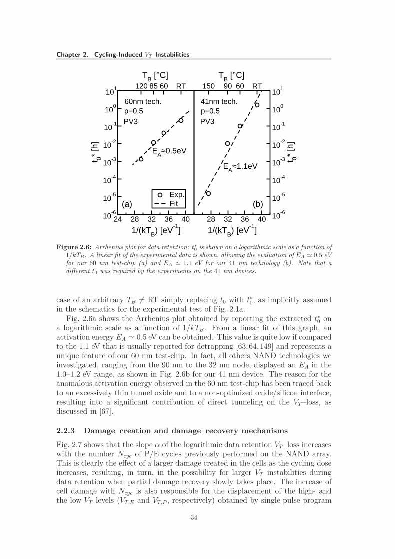
Chapter 2. Cycling-Induced VT Instabilities
24 28 32 36 40
1/(kTB) [eV-1
]
10-6
10-5
10-4
10-3
10-2
10-1
100
101
t 0* [h
]RT6085120
TB [°C]
Exp.Fit
28 32 36 40
1/(kTB) [eV-1
]
10-6
10-5
10-4
10-3
10-2
10-1
100
101
t 0* [h
]
RT6090150TB [°C]
60nm tech.
EA≈0.5eV
PV3p=0.5
EA≈1.1eV
41nm tech.p=0.5PV3
(a) (b)
Figure 2.6: Arrhenius plot for data retention: t∗
0 is shown on a logarithmic scale as a function of1/kTB. A linear fit of the experimental data is shown, allowing the evaluation of EA ≃ 0.5 eVfor our 60 nm test-chip (a) and EA ≃ 1.1 eV for our 41 nm technology (b). Note that adifferent t0 was required by the experiments on the 41 nm devices.
case of an arbitrary TB 6= RT simply replacing t0 with t∗0, as implicitly assumedin the schematics for the experimental test of Fig. 2.1a.
Fig. 2.6a shows the Arrhenius plot obtained by reporting the extracted t∗0 ona logarithmic scale as a function of 1/kTB. From a linear fit of this graph, anactivation energy EA ≃ 0.5 eV can be obtained. This value is quite low if comparedto the 1.1 eV that is usually reported for detrapping [63,64,149] and represents aunique feature of our 60 nm test-chip. In fact, all others NAND technologies weinvestigated, ranging from the 90 nm to the 32 nm node, displayed an EA in the1.0–1.2 eV range, as shown in Fig. 2.6b for our 41 nm device. The reason for theanomalous activation energy observed in the 60 nm test-chip has been traced backto an excessively thin tunnel oxide and to a non-optimized oxide/silicon interface,resulting into a significant contribution of direct tunneling on the VT –loss, asdiscussed in [67].
2.2.3 Damage–creation and damage–recovery mechanisms
Fig. 2.7 shows that the slope α of the logarithmic data retention VT –loss increaseswith the number Ncyc of P/E cycles previously performed on the NAND array.This is clearly the effect of a larger damage created in the cells as the cycling doseincreases, resulting, in turn, in the possibility for larger VT instabilities duringdata retention when partial damage recovery slowly takes place. The increase ofcell damage with Ncyc is also responsible for the displacement of the high- andthe low-VT levels (VT,E and VT,P , respectively) obtained by single-pulse program
34
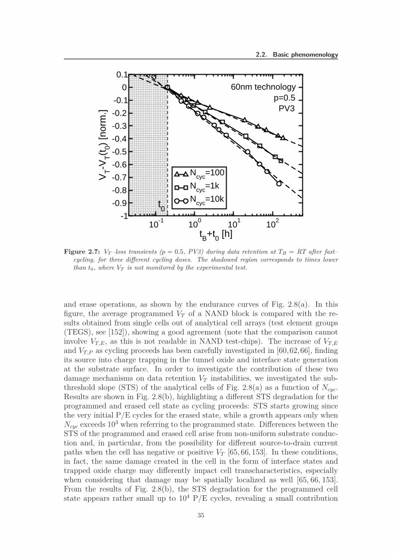
2.2. Basic phenomenology
10-1
100
101
102
tB+t0 [h]
-1
-0.9
-0.8
-0.7
-0.6
-0.5
-0.4
-0.3
-0.2
-0.1
0
0.1
VT-V
T(t
0) [n
orm
.]
Ncyc=100
Ncyc=1k
Ncyc=10k
60nm technology
PV3
t0
p=0.5
Figure 2.7: VT –loss transients (p = 0.5, PV3) during data retention at TB = RT after fast–cycling, for three different cycling doses. The shadowed region corresponds to times lowerthan t0, where VT is not monitored by the experimental test.
and erase operations, as shown by the endurance curves of Fig. 2.8(a). In thisfigure, the average programmed VT of a NAND block is compared with the re-sults obtained from single cells out of analytical cell arrays (test element groups(TEGS), see [152]), showing a good agreement (note that the comparison cannotinvolve VT,E, as this is not readable in NAND test-chips). The increase of VT,E
and VT,P as cycling proceeds has been carefully investigated in [60,62,66], findingits source into charge trapping in the tunnel oxide and interface state generationat the substrate surface. In order to investigate the contribution of these twodamage mechanisms on data retention VT instabilities, we investigated the sub-threshold slope (STS) of the analytical cells of Fig. 2.8(a) as a function of Ncyc.Results are shown in Fig. 2.8(b), highlighting a different STS degradation for theprogrammed and erased cell state as cycling proceeds: STS starts growing sincethe very initial P/E cycles for the erased state, while a growth appears only whenNcyc exceeds 103 when referring to the programmed state. Differences between theSTS of the programmed and erased cell arise from non-uniform substrate conduc-tion and, in particular, from the possibility for different source-to-drain currentpaths when the cell has negative or positive VT [65, 66, 153]. In these conditions,in fact, the same damage created in the cell in the form of interface states andtrapped oxide charge may differently impact cell transcharacteristics, especiallywhen considering that damage may be spatially localized as well [65, 66, 153].From the results of Fig. 2.8(b), the STS degradation for the programmed cellstate appears rather small up to 104 P/E cycles, revealing a small contribution
35
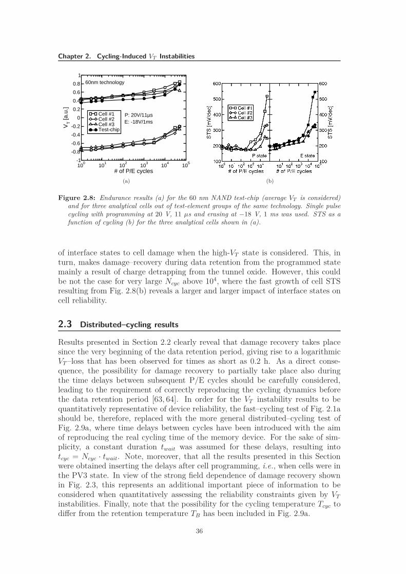
Chapter 2. Cycling-Induced VT Instabilities
100
101
102
103
104
105
# of P/E cycles
-1
-0.8
-0.6
-0.4
-0.2
0
0.2
0.4
0.6
0.8
1
VT [a
.u.]
Cell #1Cell #2Cell #3Test-chip
60nm technology
P: 20V/11µsE: -18V/1ms
(a) (b)
Figure 2.8: Endurance results (a) for the 60 nm NAND test-chip (average VT is considered)and for three analytical cells out of test-element groups of the same technology. Single pulsecycling with programming at 20 V, 11 µs and erasing at −18 V, 1 ms was used. STS as afunction of cycling (b) for the three analytical cells shown in (a).
of interface states to cell damage when the high-VT state is considered. This, inturn, makes damage–recovery during data retention from the programmed statemainly a result of charge detrapping from the tunnel oxide. However, this couldbe not the case for very large Ncyc above 104, where the fast growth of cell STSresulting from Fig. 2.8(b) reveals a larger and larger impact of interface states oncell reliability.
2.3 Distributed–cycling results
Results presented in Section 2.2 clearly reveal that damage recovery takes placesince the very beginning of the data retention period, giving rise to a logarithmicVT –loss that has been observed for times as short as 0.2 h. As a direct conse-quence, the possibility for damage recovery to partially take place also duringthe time delays between subsequent P/E cycles should be carefully considered,leading to the requirement of correctly reproducing the cycling dynamics beforethe data retention period [63, 64]. In order for the VT instability results to bequantitatively representative of device reliability, the fast–cycling test of Fig. 2.1ashould be, therefore, replaced with the more general distributed–cycling test ofFig. 2.9a, where time delays between cycles have been introduced with the aimof reproducing the real cycling time of the memory device. For the sake of sim-plicity, a constant duration twait was assumed for these delays, resulting intotcyc = Ncyc · twait. Note, moreover, that all the results presented in this Sectionwere obtained inserting the delays after cell programming, i.e., when cells were inthe PV3 state. In view of the strong field dependence of damage recovery shownin Fig. 2.3, this represents an additional important piece of information to beconsidered when quantitatively assessing the reliability constraints given by VT
instabilities. Finally, note that the possibility for the cycling temperature Tcyc todiffer from the retention temperature TB has been included in Fig. 2.9a.
36
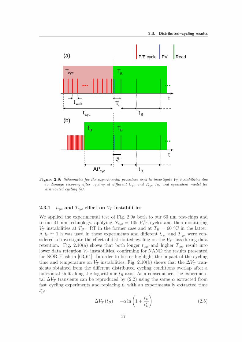
2.3. Distributed–cycling results
t*0
tB
TBTB
At*cyc
t*0
tB
TB
twait
tcyc
Tcyc
...
t
(b)
...
t
(a) PV Read
...
P/E cycle
Figure 2.9: Schematics for the experimental procedure used to investigate VT instabilities dueto damage recovery after cycling at different tcyc and Tcyc (a) and equivalent model fordistributed cycling (b).
2.3.1 tcyc and Tcyc effect on VT instabilities
We applied the experimental test of Fig. 2.9a both to our 60 nm test-chips andto our 41 nm technology, applying Ncyc = 10k P/E cycles and then monitoringVT instabilities at TB= RT in the former case and at TB = 60 oC in the latter.A t0 ≃ 1 h was used in these experiments and different tcyc and Tcyc were con-sidered to investigate the effect of distributed–cycling on the VT –loss during dataretention. Fig. 2.10(a) shows that both longer tcyc and higher Tcyc result intolower data retention VT instabilities, confirming for NAND the results presentedfor NOR Flash in [63, 64]. In order to better highlight the impact of the cyclingtime and temperature on VT instabilities, Fig. 2.10(b) shows that the ∆VT tran-sients obtained from the different distributed–cycling conditions overlap after ahorizontal shift along the logarithmic tB axis. As a consequence, the experimen-tal ∆VT transients can be reproduced by (2.2) using the same α extracted fromfast–cycling experiments and replacing t0 with an experimentally extracted timet∗B:
∆VT (tB) = −α ln
(
1 +tBt∗B
)
(2.5)
37
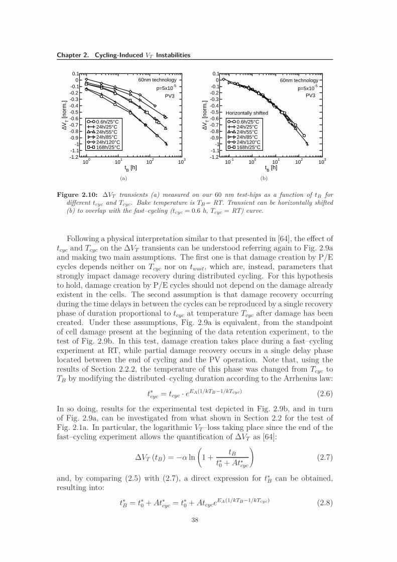
Chapter 2. Cycling-Induced VT Instabilities
100
101
102
103
tB [h]
-1.2-1.1
-1-0.9-0.8-0.7-0.6-0.5-0.4-0.3-0.2-0.1
00.1
∆VT [n
orm
.]
0.6h/25°C24h/25°C24h/55°C24h/85°C24h/120°C168h/25°C
60nm technology
p=5x10⁻⁵
PV3
(a)
10-1
100
101
102
103
tB [h]
-1.2-1.1
-1-0.9-0.8-0.7-0.6-0.5-0.4-0.3-0.2-0.1
00.1
∆VT [n
orm
.]
0.6h/25°C24h/25°C24h/55°C24h/85°C24h/120°C168h/25°C
60nm technology
p=5x10⁻⁵
PV3
Horizontally shifted
(b)
Figure 2.10: ∆VT transients (a) measured on our 60 nm test-hips as a function of tB fordifferent tcyc and Tcyc. Bake temperature is TB= RT. Transient can be horizontally shifted(b) to overlap with the fast–cycling (tcyc = 0.6 h, Tcyc = RT) curve.
Following a physical interpretation similar to that presented in [64], the effect oftcyc and Tcyc on the ∆VT transients can be understood referring again to Fig. 2.9aand making two main assumptions. The first one is that damage creation by P/Ecycles depends neither on Tcyc nor on twait, which are, instead, parameters thatstrongly impact damage recovery during distributed cycling. For this hypothesisto hold, damage creation by P/E cycles should not depend on the damage alreadyexistent in the cells. The second assumption is that damage recovery occurringduring the time delays in between the cycles can be reproduced by a single recoveryphase of duration proportional to tcyc at temperature Tcyc after damage has beencreated. Under these assumptions, Fig. 2.9a is equivalent, from the standpointof cell damage present at the beginning of the data retention experiment, to thetest of Fig. 2.9b. In this test, damage creation takes place during a fast–cyclingexperiment at RT, while partial damage recovery occurs in a single delay phaselocated between the end of cycling and the PV operation. Note that, using theresults of Section 2.2.2, the temperature of this phase was changed from Tcyc toTB by modifying the distributed–cycling duration according to the Arrhenius law:
t∗cyc = tcyc · eEA(1/kTB−1/kTcyc) (2.6)
In so doing, results for the experimental test depicted in Fig. 2.9b, and in turnof Fig. 2.9a, can be investigated from what shown in Section 2.2 for the test ofFig. 2.1a. In particular, the logarithmic VT –loss taking place since the end of thefast–cycling experiment allows the quantification of ∆VT as [64]:
∆VT (tB) = −α ln
(
1 +tB
t∗0 + At∗cyc
)
(2.7)
and, by comparing (2.5) with (2.7), a direct expression for t∗B can be obtained,resulting into:
t∗B = t∗0 + At∗cyc = t∗0 + AtcyceEA(1/kTB−1/kTcyc) (2.8)
38
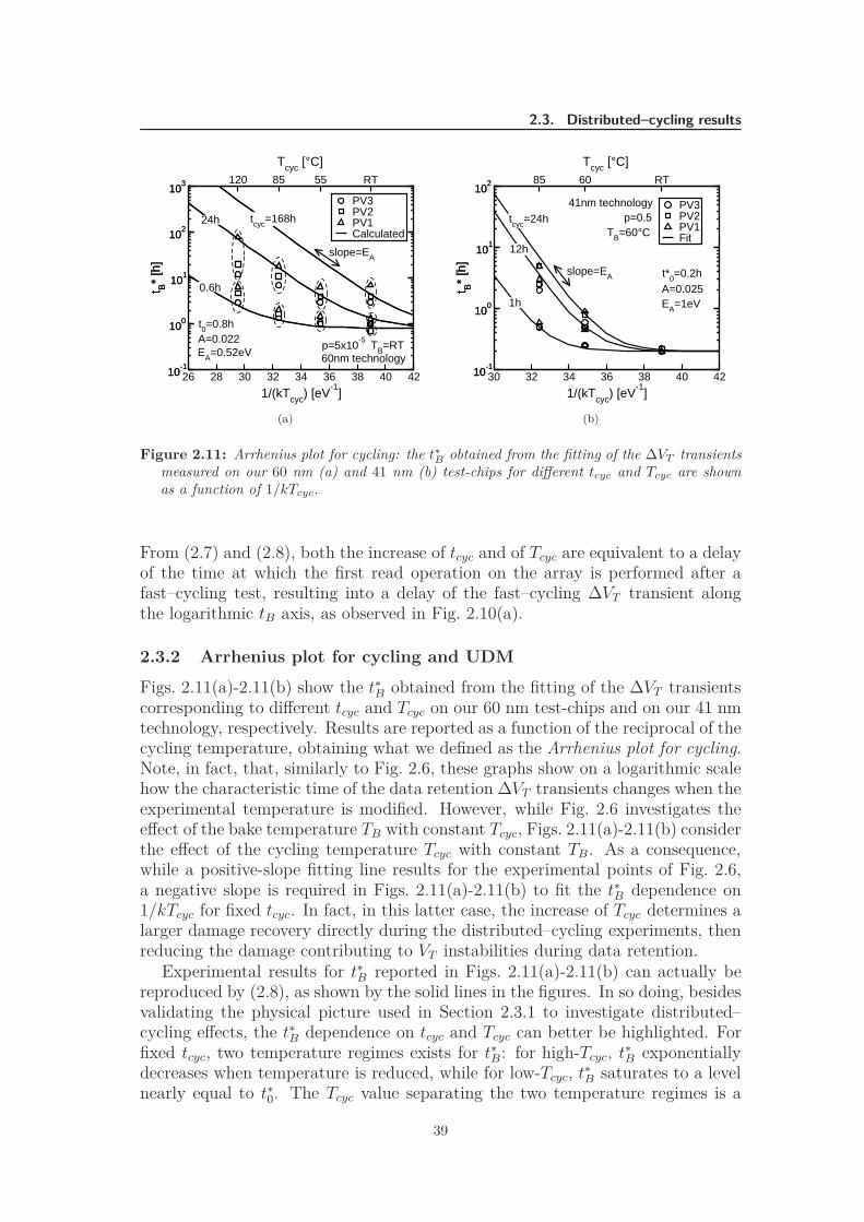
2.3. Distributed–cycling results
26 28 30 32 34 36 38 40 42
1/(kTcyc) [eV-1
]
10-1
100
101
102
103
t B*
[h]
PV3PV2PV1Calculated
RT5585120
Tcyc [°C]
10-1
100
101
102
103
t B*
[h]
tcyc=168h24h
t0=0.8h
0.6h
EA=0.52eVA=0.022
p=5x10⁻⁵
60nm technology
slope=EA
TB=RT
(a)
30 32 34 36 38 40 42
1/(kTcyc) [eV-1
]
10-1
100
101
102
t B*
[h]
PV3PV2PV1Fit
RT6085
Tcyc [°C]
10-1
100
101
102
t B*
[h]
tcyc=24h
12h
t*0=0.2h
1h EA=1eVA=0.025
p=0.541nm technology
slope=EA
TB=60°C
(b)
Figure 2.11: Arrhenius plot for cycling: the t∗
B obtained from the fitting of the ∆VT transientsmeasured on our 60 nm (a) and 41 nm (b) test-chips for different tcyc and Tcyc are shownas a function of 1/kTcyc.
From (2.7) and (2.8), both the increase of tcyc and of Tcyc are equivalent to a delayof the time at which the first read operation on the array is performed after afast–cycling test, resulting into a delay of the fast–cycling ∆VT transient alongthe logarithmic tB axis, as observed in Fig. 2.10(a).
2.3.2 Arrhenius plot for cycling and UDM
Figs. 2.11(a)-2.11(b) show the t∗B obtained from the fitting of the ∆VT transientscorresponding to different tcyc and Tcyc on our 60 nm test-chips and on our 41 nmtechnology, respectively. Results are reported as a function of the reciprocal of thecycling temperature, obtaining what we defined as the Arrhenius plot for cycling.Note, in fact, that, similarly to Fig. 2.6, these graphs show on a logarithmic scalehow the characteristic time of the data retention ∆VT transients changes when theexperimental temperature is modified. However, while Fig. 2.6 investigates theeffect of the bake temperature TB with constant Tcyc, Figs. 2.11(a)-2.11(b) considerthe effect of the cycling temperature Tcyc with constant TB. As a consequence,while a positive-slope fitting line results for the experimental points of Fig. 2.6,a negative slope is required in Figs. 2.11(a)-2.11(b) to fit the t∗B dependence on1/kTcyc for fixed tcyc. In fact, in this latter case, the increase of Tcyc determines alarger damage recovery directly during the distributed–cycling experiments, thenreducing the damage contributing to VT instabilities during data retention.
Experimental results for t∗B reported in Figs. 2.11(a)-2.11(b) can actually bereproduced by (2.8), as shown by the solid lines in the figures. In so doing, besidesvalidating the physical picture used in Section 2.3.1 to investigate distributed–cycling effects, the t∗B dependence on tcyc and Tcyc can better be highlighted. Forfixed tcyc, two temperature regimes exists for t∗B: for high-Tcyc, t
∗
B exponentiallydecreases when temperature is reduced, while for low-Tcyc, t
∗
B saturates to a levelnearly equal to t∗0. The Tcyc value separating the two temperature regimes is a
39
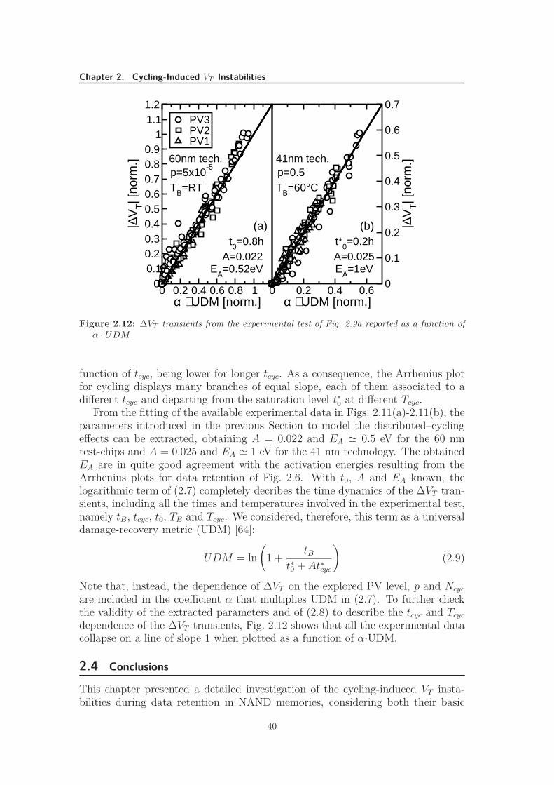
Chapter 2. Cycling-Induced VT Instabilities
0 0.2 0.4 0.6 0.8 1α ⋅ UDM [norm.]
00.10.20.30.40.50.60.70.80.9
11.11.2
|∆V
T| [
norm
.]PV3PV2PV1
0 0.2 0.4 0.6α ⋅ UDM [norm.]
0
0.1
0.2
0.3
0.4
0.5
0.6
0.7
|∆V
T| [
norm
.]
A=0.022
p=5x10⁻⁵
60nm tech.
t0=0.8h
EA=0.52eV EA=1eV
t*0=0.2hA=0.025
41nm tech.p=0.5
TB=RT TB=60°C
(a) (b)
Figure 2.12: ∆VT transients from the experimental test of Fig. 2.9a reported as a function ofα · UDM .
function of tcyc, being lower for longer tcyc. As a consequence, the Arrhenius plotfor cycling displays many branches of equal slope, each of them associated to adifferent tcyc and departing from the saturation level t∗0 at different Tcyc.
From the fitting of the available experimental data in Figs. 2.11(a)-2.11(b), theparameters introduced in the previous Section to model the distributed–cyclingeffects can be extracted, obtaining A = 0.022 and EA ≃ 0.5 eV for the 60 nmtest-chips and A = 0.025 and EA ≃ 1 eV for the 41 nm technology. The obtainedEA are in quite good agreement with the activation energies resulting from theArrhenius plots for data retention of Fig. 2.6. With t0, A and EA known, thelogarithmic term of (2.7) completely decribes the time dynamics of the ∆VT tran-sients, including all the times and temperatures involved in the experimental test,namely tB, tcyc, t0, TB and Tcyc. We considered, therefore, this term as a universaldamage-recovery metric (UDM) [64]:
UDM = ln
(
1 +tB
t∗0 + At∗cyc
)
(2.9)
Note that, instead, the dependence of ∆VT on the explored PV level, p and Ncyc
are included in the coefficient α that multiplies UDM in (2.7). To further checkthe validity of the extracted parameters and of (2.8) to describe the tcyc and Tcyc
dependence of the ∆VT transients, Fig. 2.12 shows that all the experimental datacollapse on a line of slope 1 when plotted as a function of α·UDM.
2.4 Conclusions
This chapter presented a detailed investigation of the cycling-induced VT insta-bilities during data retention in NAND memories, considering both their basic
40
2.4. Conclusions
phenomenology and how they change when modifying tcyc and Tcyc. Instabilitiesfrom the programmed state were shown to manifest themselves as a VT –loss thatlogarithmically increases with the total time elapsed since the end of cycling. Theslope of the logarithmic discharge was shown to depend on the electric field dur-ing data retention, the cycling dose and the probability level at which the arraycumulative distribution is monitored. Changes in tcyc, Tcyc and TB correspond,instead, to an equivalent change of the instant at which the first read operationon the array is performed. Considering a large variety of tcyc and Tcyc, the param-eters needed to model the distributed–cycling effects on NAND were extracted,similarly to what done for NOR in [64].
41

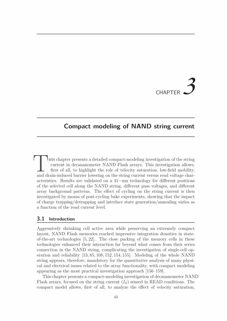
CHAPTER3
Compact modeling of NAND string current
This chapter presents a detailed compact-modeling investigation of the stringcurrent in decananometer NAND Flash arrays. This investigation allows,first of all, to highlight the role of velocity saturation, low-field mobility,
and drain-induced barrier lowering on the string current versus read voltage char-acteristics. Results are validated on a 41−nm technology for different positionsof the selected cell along the NAND string, different pass voltages, and differentarray background patterns. The effect of cycling on the string current is theninvestigated by means of post-cycling bake experiments, showing that the impactof charge trapping/detrapping and interface state generation/annealing varies asa function of the read current level.
3.1 Introduction
Aggressively shrinking cell active area while preserving an extremely compactlayout, NAND Flash memories reached impressive integration densities in state-of-the-art technologies [5, 22]. The close packing of the memory cells in thesetechnologies enhanced their interaction far beyond what comes from their seriesconnection in the NAND string, complicating the investigation of single-cell op-eration and reliability [13, 85, 108, 152, 154, 155]. Modeling of the whole NANDstring appears, therefore, mandatory for the quantitative analysis of many physi-cal and electrical issues related to the array functionality, with compact modelingappearing as the most practical investigation approach [156–159].
This chapter presents a compact-modeling investigation of decananometer NANDFlash arrays, focused on the string current (IS) sensed in READ conditions. Thecompact model allows, first of all, to analyze the effect of velocity saturation,
43
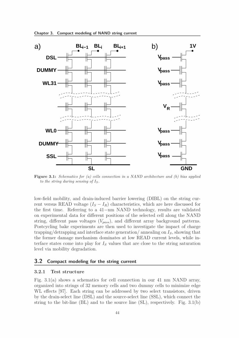
Chapter 3. Compact modeling of NAND string current
BL i BLBL 1V
Vpass
Vpass
Vpass
Vpass
Vpass
Vpass
DUMMY
WL31
WL0
SSL
DUMMY
DSL
V
i+1
GNDSL
i−1
R
a) b)
Figure 3.1: Schematics for (a) cells connection in a NAND architecture and (b) bias appliedto the string during sensing of IS .
low-field mobility, and drain-induced barrier lowering (DIBL) on the string cur-rent versus READ voltage (IS − IR) characteristics, which are here discussed forthe first time. Referring to a 41−nm NAND technology, results are validatedon experimental data for different positions of the selected cell along the NANDstring, different pass voltages (Vpass), and different array background patterns.Postcycling bake experiments are then used to investigate the impact of chargetrapping/detrapping and interface state generation/ annealing on IS, showing thatthe former damage mechanism dominates at low READ current levels, while in-terface states come into play for IS values that are close to the string saturationlevel via mobility degradation.
3.2 Compact modeling for the string current
3.2.1 Test structure
Fig. 3.1(a) shows a schematics for cell connection in our 41 nm NAND array,organized into strings of 32 memory cells and two dummy cells to minimize edgeWL effects [97]. Each string can be addressed by two select transistors, drivenby the drain-select line (DSL) and the source-select line (SSL), which connect thestring to the bit-line (BL) and to the source line (SL), respectively. Fig. 3.1(b)
44
3.2. Compact modeling for the string current
Figure 3.2: Schematic cross section of a NAND array along (left) the bit line and (right) theWL directions, highlighting the main capacitive couplings of the floating gates.
shows the bias conditions used in this paper for IS investigation: a variable VR isapplied to the selected cell WL during READ, with not only all other WLs butalso the DSL and SSL at Vpass. A 1 − V bias was applied to the BL, with the SLgrounded.
3.2.2 Electrostatics
Fig. 3.2 shows a schematic cross section of the NAND array along the BL andWL directions, highlighting the main capacitive couplings of the floating gates.Due to the close packing of the array cells, parasitic couplings between adjacentfloating gates have a non-negligible impact on their potential, which for i-th cellalong the string (V i
F G), was computed from
V iF G = αGV
iW L + αSV
iS + αDV
iD +
QiF G
CT OT+
+ αx
(
V i,LF G + V i,R
F G
)
+ αy
(
V i+1F G + V i−1
F G
)
+
+ αW L
(
V i+1W L + V i−1
W L
)
(3.1)
The coupling coefficients αG, αS and αD in (3.1) are given by the capacitancebetween the floating gate and its WL, source and drain, respectively, divided bythe total floating gate capacitance CT OT . Similarly, αx and αy are the ratiosbetween Cx and Cy (see Fig. 3.2) and CT OT , accounting for inter-floating-gate
coupling in the WL direction (with adjacent FGs at potentials Vi,L/R
F G ) and inthe BL direction (with adjacent FGs at potentials V i±1
F G ). The parameter αW L
accounts for the direct parasitic coupling between a floating gate and its adjacentWLs (at potentials V i±1
W L ). All the previous coupling coefficients were evaluatedby TCAD simulations of a 3 × 3 cell structure.
The relation between V iF G and surface potentials ψi
s for the i-th cell is given
45
Chapter 3. Compact modeling of NAND string current
by [156,159]:
V iF G = VF B + ψi
s +
√
2ǫSiqNA(V iS + ψi
s)
Cox− θV i
DS (3.2)
where VF B is the flatband voltage, Cox the tunnel oxide capacitance, ǫSi the silicondielectric constant, q is the electron charge, NA is the substrate doping and V i
DS
is the drain-source voltage of the i-th cell. The fitting parameter θ models theDIBL effect and also partially accounts for channel-length modulation effects. Theelectrostatic threshold voltage V F G,i
T of the equivalent transistor, correspondingto the floating-gate bias bringing the cell into the strong-inversion regime, can becalculated from (3.2) assuming ψs = 2ψB, ψB being the distance of the Fermi levelin the bulk and the V i
S term allowing the body effect to be correctly included inour model.
3.2.3 Conduction and mobility model
The drain current of the i-th cell along the NAND string was calculated accordingto conventional MOSFET models for the strong-inversion (I i
D,SI) and subthreshold
regimes (I iD,sub) [160]:
I iD,SI = −Wvd(y)Qi
inv
(
V iF G, V
F G,iT , V i(y), V i
S
)
(3.3)
I isub =µeff
W
L
√
ǫSiqNa
2ψis
(
kT
q
)2 (ni
Na
)2
exp
[
q (ψis − V i
S)
kT
](
1 − exp
[
−qV iDS
kT
]) (3.4)
where W and L are the cell width and length, vd(y) and V i(y) are the electronvelocity and the electron quasi-Fermi potential in the source-to-drain (y) direction,Qi
inv is the electron charge in the channel, ni is the intrinsic carrier concentration,and kT is the thermal energy. The total drain current was modeled as.
I iD = I i
D,SI + I iD,sub (3.5)
provided that I iD,sub is limited in the strong-inversion regime as done in [156] to
account for the pinning of surface potential.To take into account vd saturation at high longitudinal electric fields Ey, the
following well-known relationship was used [160]:
vd =µeff
[
1 +(
Eyµeff
vsat
)2]1/2
Ey (3.6)
where vsat = 8x106 cm s−1 is the electron saturation velocity in MOSFET chan-nels [160]. The dependence of the low-field electron mobility µeff in (3.6) onthe effective normal electric field Eeff was described according to the empiricalmodel [161, 162]:
µeff =µ0
1 +(
Eeff
E0
)ν (3.7)
46
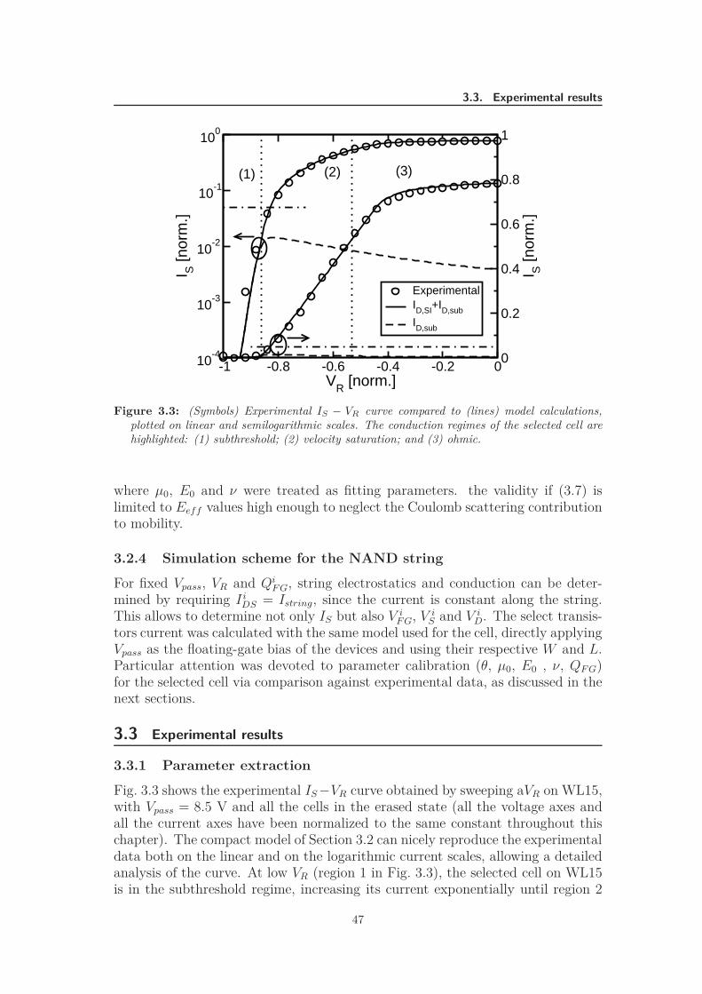
3.3. Experimental results
-1 -0.8 -0.6 -0.4 -0.2 0VR [norm.]
0
0.2
0.4
0.6
0.8
1
I S [n
orm
.]
10-4
10-3
10-2
10-1
100
I S [n
orm
.]
ExperimentalID,SI+ID,sub
ID,sub
(1) (2) (3)
Figure 3.3: (Symbols) Experimental IS − VR curve compared to (lines) model calculations,plotted on linear and semilogarithmic scales. The conduction regimes of the selected cell arehighlighted: (1) subthreshold; (2) velocity saturation; and (3) ohmic.
where µ0, E0 and ν were treated as fitting parameters. the validity if (3.7) islimited to Eeff values high enough to neglect the Coulomb scattering contributionto mobility.
3.2.4 Simulation scheme for the NAND string
For fixed Vpass, VR and QiF G, string electrostatics and conduction can be deter-
mined by requiring I iDS = Istring, since the current is constant along the string.
This allows to determine not only IS but also V iF G, V i
S and V iD. The select transis-
tors current was calculated with the same model used for the cell, directly applyingVpass as the floating-gate bias of the devices and using their respective W and L.Particular attention was devoted to parameter calibration (θ, µ0, E0 , ν, QF G)for the selected cell via comparison against experimental data, as discussed in thenext sections.
3.3 Experimental results
3.3.1 Parameter extraction
Fig. 3.3 shows the experimental IS −VR curve obtained by sweeping aVR on WL15,with Vpass = 8.5 V and all the cells in the erased state (all the voltage axes andall the current axes have been normalized to the same constant throughout thischapter). The compact model of Section 3.2 can nicely reproduce the experimentaldata both on the linear and on the logarithmic current scales, allowing a detailedanalysis of the curve. At low VR (region 1 in Fig. 3.3), the selected cell on WL15is in the subthreshold regime, increasing its current exponentially until region 2
47
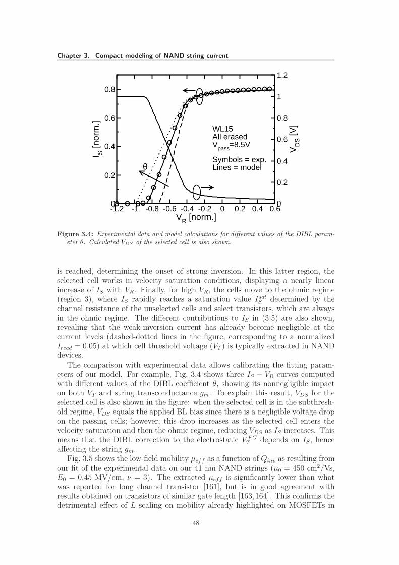
Chapter 3. Compact modeling of NAND string current
-1.2 -1 -0.8 -0.6 -0.4 -0.2 0 0.2 0.4 0.6VR [norm.]
0
0.2
0.4
0.6
0.8I S
[nor
m.]
0
0.2
0.4
0.6
0.8
1
1.2
VD
S [V
]WL15All erasedVpass=8.5V
Symbols = exp.Lines = modelθ
Figure 3.4: Experimental data and model calculations for different values of the DIBL param-eter θ. Calculated VDS of the selected cell is also shown.
is reached, determining the onset of strong inversion. In this latter region, theselected cell works in velocity saturation conditions, displaying a nearly linearincrease of IS with VR. Finally, for high VR, the cells move to the ohmic regime(region 3), where IS rapidly reaches a saturation value Isat
S determined by thechannel resistance of the unselected cells and select transistors, which are alwaysin the ohmic regime. The different contributions to IS in (3.5) are also shown,revealing that the weak-inversion current has already become negligible at thecurrent levels (dashed-dotted lines in the figure, corresponding to a normalizedIread = 0.05) at which cell threshold voltage (VT ) is typically extracted in NANDdevices.
The comparison with experimental data allows calibrating the fitting param-eters of our model. For example, Fig. 3.4 shows three IS − VR curves computedwith different values of the DIBL coefficient θ, showing its nonnegligible impacton both VT and string transconductance gm. To explain this result, VDS for theselected cell is also shown in the figure: when the selected cell is in the subthresh-old regime, VDS equals the applied BL bias since there is a negligible voltage dropon the passing cells; however, this drop increases as the selected cell enters thevelocity saturation and then the ohmic regime, reducing VDS as IS increases. Thismeans that the DIBL correction to the electrostatic V F G
T depends on IS, henceaffecting the string gm.
Fig. 3.5 shows the low-field mobility µeff as a function of Qinv as resulting fromour fit of the experimental data on our 41 nm NAND strings (µ0 = 450 cm2/Vs,E0 = 0.45 MV/cm, ν = 3). The extracted µeff is significantly lower than whatwas reported for long channel transistor [161], but is in good agreement withresults obtained on transistors of similar gate length [163,164]. This confirms thedetrimental effect of L scaling on mobility already highlighted on MOSFETs in
48
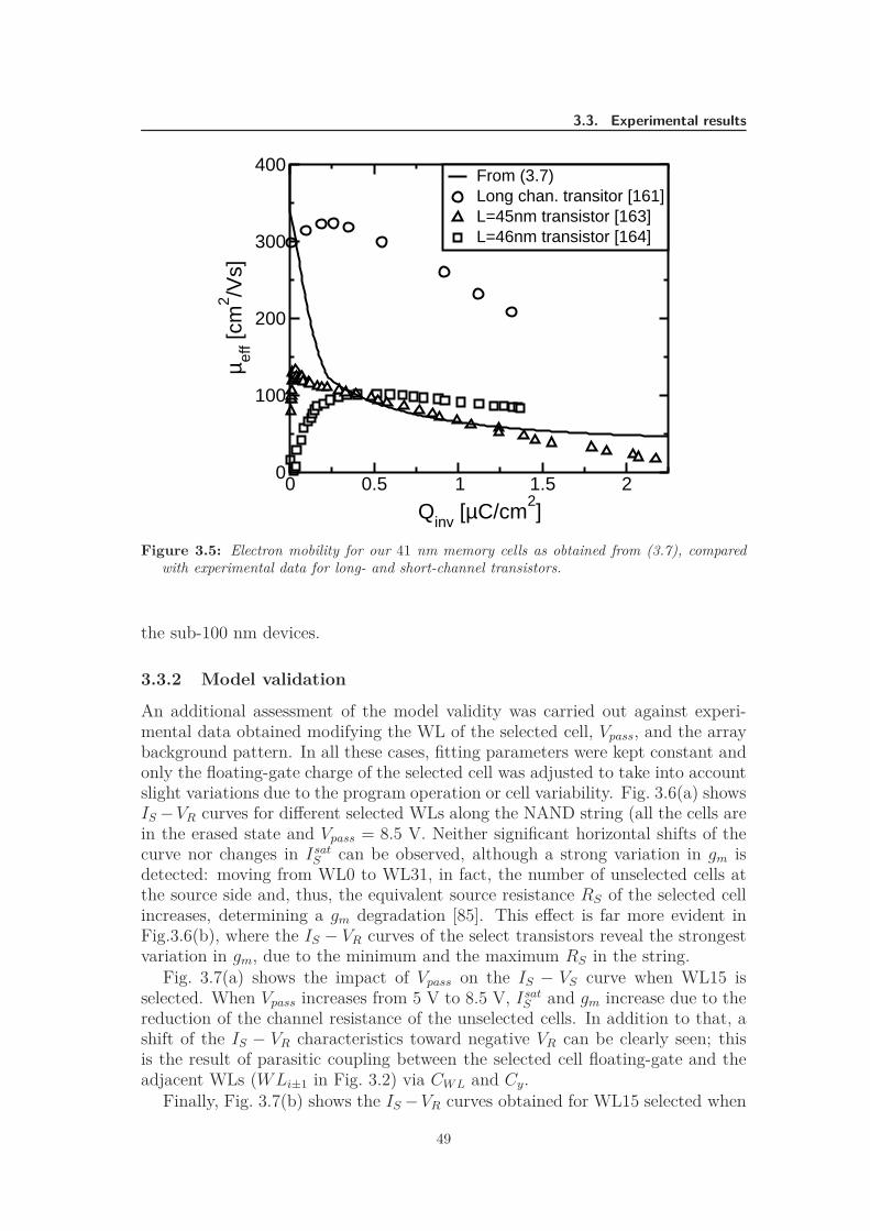
3.3. Experimental results
0 0.5 1 1.5 2
Qinv [µC/cm2]
0
100
200
300
400
µ eff [c
m2 /V
s]
From (3.7)Long chan. transitor [161]L=45nm transistor [163]L=46nm transistor [164]
Figure 3.5: Electron mobility for our 41 nm memory cells as obtained from (3.7), comparedwith experimental data for long- and short-channel transistors.
the sub-100 nm devices.
3.3.2 Model validation
An additional assessment of the model validity was carried out against experi-mental data obtained modifying the WL of the selected cell, Vpass, and the arraybackground pattern. In all these cases, fitting parameters were kept constant andonly the floating-gate charge of the selected cell was adjusted to take into accountslight variations due to the program operation or cell variability. Fig. 3.6(a) showsIS −VR curves for different selected WLs along the NAND string (all the cells arein the erased state and Vpass = 8.5 V. Neither significant horizontal shifts of thecurve nor changes in Isat
S can be observed, although a strong variation in gm isdetected: moving from WL0 to WL31, in fact, the number of unselected cells atthe source side and, thus, the equivalent source resistance RS of the selected cellincreases, determining a gm degradation [85]. This effect is far more evident inFig.3.6(b), where the IS − VR curves of the select transistors reveal the strongestvariation in gm, due to the minimum and the maximum RS in the string.
Fig. 3.7(a) shows the impact of Vpass on the IS − VS curve when WL15 isselected. When Vpass increases from 5 V to 8.5 V, Isat
S and gm increase due to thereduction of the channel resistance of the unselected cells. In addition to that, ashift of the IS − VR characteristics toward negative VR can be clearly seen; thisis the result of parasitic coupling between the selected cell floating-gate and theadjacent WLs (WLi±1 in Fig. 3.2) via CW L and Cy.
Finally, Fig. 3.7(b) shows the IS −VR curves obtained for WL15 selected when
49
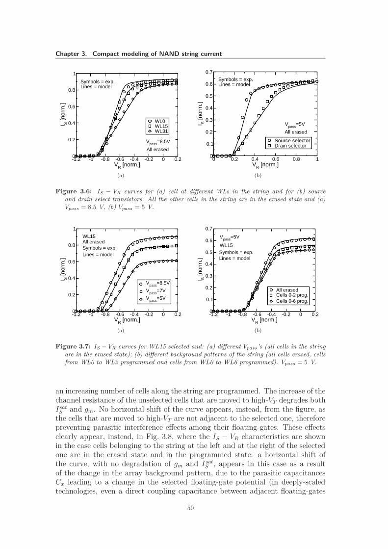
Chapter 3. Compact modeling of NAND string current
-1.2 -1 -0.8 -0.6 -0.4 -0.2 0 0.2VR [norm.]
0
0.2
0.4
0.6
0.8
1
I S [n
orm
.]
WL0WL15WL31
Vpass=8.5V
All erased
Symbols = exp. Lines = model
(a)
0 0.2 0.4 0.6 0.8 1VR [norm.]
0
0.1
0.2
0.3
0.4
0.5
0.6
0.7
I S [n
orm
.]
Source selectorDrain selector
Vpass=5V
Symbols = exp.Lines = model
All erased
(b)
Figure 3.6: IS − VR curves for (a) cell at different WLs in the string and for (b) sourceand drain select transistors. All the other cells in the string are in the erased state and (a)Vpass = 8.5 V, (b) Vpass = 5 V.
-1.2 -1 -0.8 -0.6 -0.4 -0.2 0 0.2VR [norm.]
0
0.2
0.4
0.6
0.8
1
I S [n
orm
.]
Vpass=8.5V
Vpass=7V
Vpass=5V
All erasedSymbols = exp.Lines = model
WL15
(a)
-1.2 -1 -0.8 -0.6 -0.4 -0.2 0 0.2VR [norm.]
0
0.1
0.2
0.3
0.4
0.5
0.6
0.7
I S [n
orm
.]
All erasedCells 0-2 prog.Cells 0-6 prog.
Vpass=5V
WL15Symbols = exp.Lines = model
(b)
Figure 3.7: IS − VR curves for WL15 selected and: (a) different Vpass’s (all cells in the stringare in the erased state); (b) different background patterns of the string (all cells erased, cellsfrom WL0 to WL2 programmed and cells from WL0 to WL6 programmed). Vpass = 5 V.
an increasing number of cells along the string are programmed. The increase of thechannel resistance of the unselected cells that are moved to high-VT degrades bothIsat
S and gm. No horizontal shift of the curve appears, instead, from the figure, asthe cells that are moved to high-VT are not adjacent to the selected one, thereforepreventing parasitic interference effects among their floating-gates. These effectsclearly appear, instead, in Fig. 3.8, where the IS − VR characteristics are shownin the case cells belonging to the string at the left and at the right of the selectedone are in the erased state and in the programmed state: a horizontal shift ofthe curve, with no degradation of gm and Isat
S , appears in this case as a resultof the change in the array background pattern, due to the parasitic capacitancesCx leading to a change in the selected floating-gate potential (in deeply-scaledtechnologies, even a direct coupling capacitance between adjacent floating-gates
50
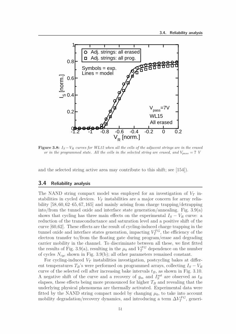
3.4. Reliability analysis
-1.2 -1 -0.8 -0.6 -0.4 -0.2 0 0.2VR [norm.]
0
0.2
0.4
0.6
0.8
1
I S [n
orm
.]
Adj. strings: all erasedAdj. strings: all prog.
WL15All erased
Vpass=7V
Symbols = exp.Lines = model
Figure 3.8: IS −VR curves for WL15 when all the cells of the adjacent strings are in the erasedor in the programmed state. All the cells in the selected string are erased, and Vpass = 7 V
and the selected string active area may contribute to this shift; see [154]).
3.4 Reliability analysis
The NAND string compact model was employed for an investigation of VT in-stabilities in cycled devices. VT instabilities are a major concern for array relia-bility [58, 60, 62–65, 67, 165] and mainly arising from charge trapping/detrappinginto/from the tunnel oxide and interface state generation/annealing. Fig. 3.9(a)shows that cycling has three main effects on the experimental IS − VR curve: areduction of the transconductance and saturation level and a positive shift of thecurve [60,62]. These effects are the result of cycling-induced charge trapping in thetunnel oxide and interface states generation, impacting V F G
T , the efficiency of theelectron transfer to/from the floating gate during program/erase and degradingcarrier mobility in the channel. To discriminate between all these, we first fittedthe results of Fig. 3.9(a), resulting in the µ0 and V F G
T dependence on the numberof cycles Ncyc shown in Fig. 3.9(b); all other parameters remained constant.
For cycling-induced VT instabilities investigation, postcycling bakes at differ-ent temperatures TB’s were performed on programmed arrays, collecting IS − VR
curve of the selected cell after increasing bake intervals tB, as shown in Fig. 3.10.A negative shift of the curve and a recovery of gm and Isat
S are observed as tBelapses, these effects being more pronounced for higher TB and revealing that theunderlying physical phenomena are thermally activated. Experimental data werefitted by the NAND string compact model by changing µ0, to take into accountmobility degradation/recovery dynamics, and introducing a term ∆V F G
T , generi-
51
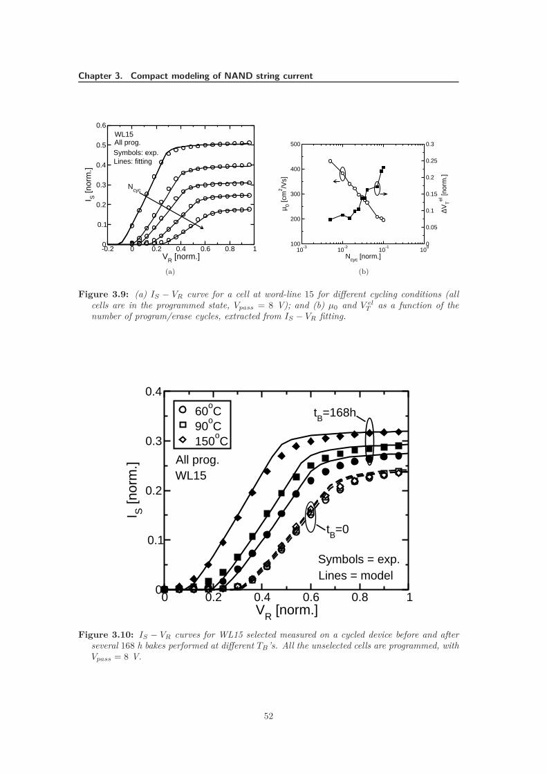
Chapter 3. Compact modeling of NAND string current
-0.2 0 0.2 0.4 0.6 0.8 1VR [norm.]
0
0.1
0.2
0.3
0.4
0.5
0.6
I S [n
orm
.]
Ncyc
WL15All prog.Symbols: exp.Lines: fitting
(a)
10-3
10-2
10-1
100
Ncyc [norm.]
100
200
300
400
500
µ 0 [cm
2 /Vs]
0
0.05
0.1
0.15
0.2
0.25
0.3
∆VT
el [n
orm
.]
(b)
Figure 3.9: (a) IS − VR curve for a cell at word-line 15 for different cycling conditions (allcells are in the programmed state, Vpass = 8 V); and (b) µ0 and V el
T as a function of thenumber of program/erase cycles, extracted from IS − VR fitting.
0 0.2 0.4 0.6 0.8 1VR [norm.]
0
0.1
0.2
0.3
0.4
I S [n
orm
.]
60oC
90oC
150oC
WL15All prog.
Symbols = exp.Lines = model
tB=0
tB=168h
Figure 3.10: IS − VR curves for WL15 selected measured on a cycled device before and afterseveral 168 h bakes performed at different TB’s. All the unselected cells are programmed, withVpass = 8 V.
52
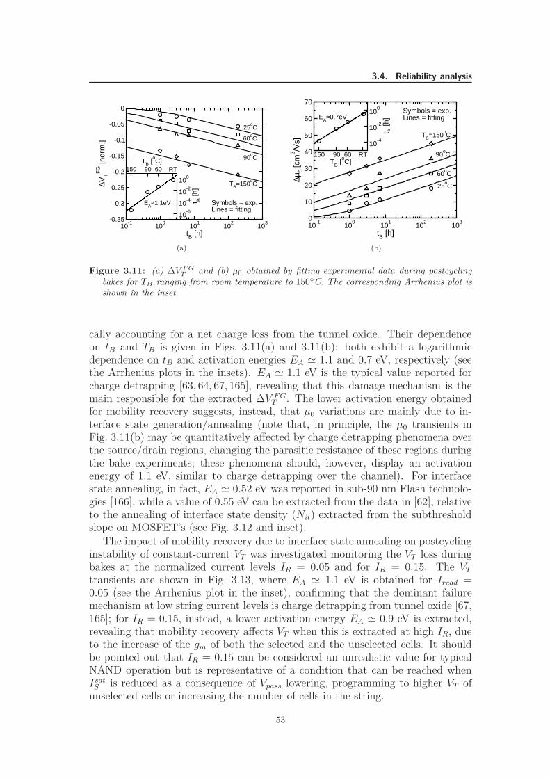
3.4. Reliability analysis
10-1
100
101
102
103
tB [h]
-0.35
-0.3
-0.25
-0.2
-0.15
-0.1
-0.05
0∆V
TF
G [n
orm
.]
10-6
10-4
10-2
100
t B [h
]
150 60 RT90TB [
oC]
TB=150oC
90oC
60oC
25oC
EA≈1.1eV Symbols = exp.Lines = fitting
(a)
10-1
100
101
102
103
tB [h]
0
10
20
30
40
50
60
70
∆µ0
[cm
2 /Vs] 10
-4
10-2
100
t B [h
]
150 60 RT90TB [
oC]
TB=150oC
90oC
60oC
25oC
EA≈0.7eVSymbols = exp.Lines = fitting
(b)
Figure 3.11: (a) ∆V F GT and (b) µ0 obtained by fitting experimental data during postcycling
bakes for TB ranging from room temperature to 150◦C. The corresponding Arrhenius plot isshown in the inset.
cally accounting for a net charge loss from the tunnel oxide. Their dependenceon tB and TB is given in Figs. 3.11(a) and 3.11(b): both exhibit a logarithmicdependence on tB and activation energies EA ≃ 1.1 and 0.7 eV, respectively (seethe Arrhenius plots in the insets). EA ≃ 1.1 eV is the typical value reported forcharge detrapping [63, 64, 67, 165], revealing that this damage mechanism is themain responsible for the extracted ∆V F G
T . The lower activation energy obtainedfor mobility recovery suggests, instead, that µ0 variations are mainly due to in-terface state generation/annealing (note that, in principle, the µ0 transients inFig. 3.11(b) may be quantitatively affected by charge detrapping phenomena overthe source/drain regions, changing the parasitic resistance of these regions duringthe bake experiments; these phenomena should, however, display an activationenergy of 1.1 eV, similar to charge detrapping over the channel). For interfacestate annealing, in fact, EA ≃ 0.52 eV was reported in sub-90 nm Flash technolo-gies [166], while a value of 0.55 eV can be extracted from the data in [62], relativeto the annealing of interface state density (Nit) extracted from the subthresholdslope on MOSFET’s (see Fig. 3.12 and inset).
The impact of mobility recovery due to interface state annealing on postcyclinginstability of constant-current VT was investigated monitoring the VT loss duringbakes at the normalized current levels IR = 0.05 and for IR = 0.15. The VT
transients are shown in Fig. 3.13, where EA ≃ 1.1 eV is obtained for Iread =0.05 (see the Arrhenius plot in the inset), confirming that the dominant failuremechanism at low string current levels is charge detrapping from tunnel oxide [67,165]; for IR = 0.15, instead, a lower activation energy EA ≃ 0.9 eV is extracted,revealing that mobility recovery affects VT when this is extracted at high IR, dueto the increase of the gm of both the selected and the unselected cells. It shouldbe pointed out that IR = 0.15 can be considered an unrealistic value for typicalNAND operation but is representative of a condition that can be reached whenIsat
S is reduced as a consequence of Vpass lowering, programming to higher VT ofunselected cells or increasing the number of cells in the string.
53
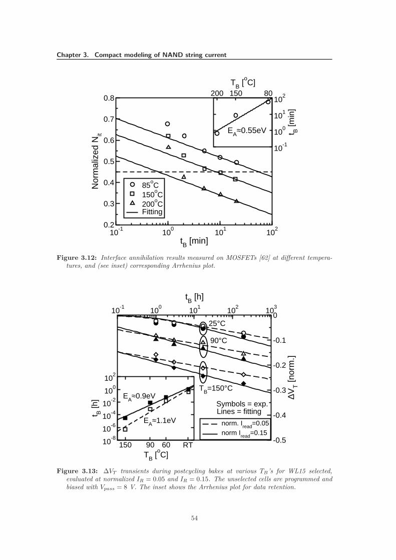
Chapter 3. Compact modeling of NAND string current
10-1
100
101
102
tB [min]
0.2
0.3
0.4
0.5
0.6
0.7
0.8N
orm
aliz
ed N
it
85oC
150oC
200oC
Fitting
80150200TB [
oC]
10-1
100
101
102
t B [m
in]
EA≈0.55eV
Figure 3.12: Interface annihilation results measured on MOSFETs [62] at different tempera-tures, and (see inset) corresponding Arrhenius plot.
10-1
100
101
102
103
tB [h]
-0.5
-0.4
-0.3
-0.2
-0.1
0
∆VT [n
orm
.]
norm. Iread=0.05norm Iread=0.15
150 90 60 RTTB [
oC]
10-8
10-6
10-4
10-2
100
102
t B [h
]
25°C
90°C
TB=150°C
Symbols = exp.Lines = fitting
EA≈1.1eV
EA≈0.9eV
Figure 3.13: ∆VT transients during postcycling bakes at various TB’s for WL15 selected,evaluated at normalized IR = 0.05 and IR = 0.15. The unselected cells are programmed andbiased with Vpass = 8 V. The inset shows the Arrhenius plot for data retention.
54
3.5. Conclusions
3.5 Conclusions
This chapter presented a detailed compact-modeling investigation of the IS −VR characteristics in decananometer NAND strings Flash arrays. The role ofvelocity saturation, low-field mobility and DIBL on IS were discussed, validatingthe results on experimental data for a 41−nm technology. Then, the compactmodel was used to analyze the contribution of charge trapping/detrapping andinterface states on IS and on cycling-induced VT instabilities, revealing that thelatter comes into play when cell VT is monitored at high IR, due to carrier mobilitydegradation. Results show that VT instabilities are increased and their activationenergy is lowered with respect to the usual 1.1 eV value given by charge detrappingwhenever the saturation value of Istring moves too close to Iread.
55

CHAPTER4
Distributed-cycling schemes for NOR Flash arrays
This chapter investigates the validity of distributed-cycling schemes on scaledFlash memory technologies. These schemes rely on the possibility to em-ulate on-field device operation by increasing the cycling temperature ac-
cording to an Arrhenius law, but the assessment of the activation energy that hasto be used on scaled technologies requires a careful control of the experimentaltests, preventing spurious second-order effects to emerge. In particular, long gate-stresses required to gather the array threshold voltage (VT ) map are shown to giverise to parasitic VT -drifts, which add to the VT -loss coming from damage recoveryduring post-cycling bake. When the superposition of the two phenomena is takeninto account, the effectiveness of the conventional qualification schemes relying ona 1.1 eV activation energy is fully confirmed at the 45 nm NOR node.
4.1 Introduction
Floating-gate devices are the most widely used non-volatile semiconductor mem-ories, thanks to their high density and good performance, in terms of throughputand data retention [5,167,168]. The demand for ever higher storage densities hasled to a continuous cell scaling and to the development of multi-level (MLC) tech-nologies [169–171], leading to an increased sensitivity to spurious charges trappedin the dielectrics (e.g., a single charge trapped in the tunnel oxide can give aVT -shift of 100 mV in state-of-the-art NAND cells [5]). For this reason, VT insta-bilities during post-cycling bakes emerged as one of the major reliability concernsfor decananometer Flash technologies [63, 64, 67, 165] and great efforts have beenspent to develop adequate qualification tests [172–174]. These instabilities are dueto charge trapping/detrapping into/from the tunnel oxide and interface states an-
57
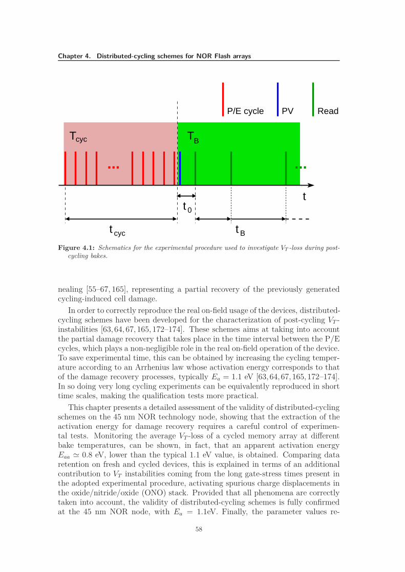
Chapter 4. Distributed-cycling schemes for NOR Flash arrays
P/E cycle PV
t cyc
Tcyc
t B
t 0
TB
...
t
...
Read
Figure 4.1: Schematics for the experimental procedure used to investigate VT -loss during post-cycling bakes.
nealing [55–67, 165], representing a partial recovery of the previously generatedcycling-induced cell damage.
In order to correctly reproduce the real on-field usage of the devices, distributed-cycling schemes have been developed for the characterization of post-cycling VT -instabilities [63, 64, 67, 165, 172–174]. These schemes aims at taking into accountthe partial damage recovery that takes place in the time interval between the P/Ecycles, which plays a non-negligible role in the real on-field operation of the device.To save experimental time, this can be obtained by increasing the cycling temper-ature according to an Arrhenius law whose activation energy corresponds to thatof the damage recovery processes, typically Ea = 1.1 eV [63,64, 67, 165, 172–174].In so doing very long cycling experiments can be equivalently reproduced in shorttime scales, making the qualification tests more practical.
This chapter presents a detailed assessment of the validity of distributed-cyclingschemes on the 45 nm NOR technology node, showing that the extraction of theactivation energy for damage recovery requires a careful control of experimen-tal tests. Monitoring the average VT -loss of a cycled memory array at differentbake temperatures, can be shown, in fact, that an apparent activation energyEaa ≃ 0.8 eV, lower than the typical 1.1 eV value, is obtained. Comparing dataretention on fresh and cycled devices, this is explained in terms of an additionalcontribution to VT instabilities coming from the long gate-stress times present inthe adopted experimental procedure, activating spurious charge displacements inthe oxide/nitride/oxide (ONO) stack. Provided that all phenomena are correctlytaken into account, the validity of distributed-cycling schemes is fully confirmedat the 45 nm NOR node, with Ea = 1.1eV. Finally, the parameter values re-
58
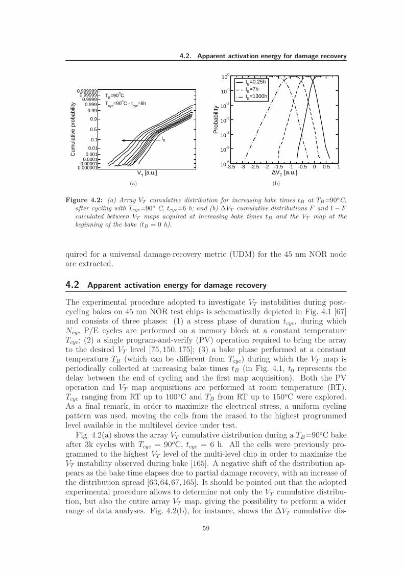
4.2. Apparent activation energy for damage recovery
VT [a.u.]
0.000010.0001
0.0010.01
0.1
0.5
0.9
0.990.999
0.99990.99999
0.000001
0.999999
Cum
ulat
ive
prob
abili
ty
tB
Tcyc=90oC - tcyc=6h
TB=90oC
(a)
-3.5 -3 -2.5 -2 -1.5 -1 -0.5 0 0.5 1∆VT [a.u.]
10-6
10-5
10-4
10-3
10-2
10-1
100
Pro
babi
lity
tB=0.25htB=7htB=1300h
(b)
Figure 4.2: (a) Array VT cumulative distribution for increasing bake times tB at TB=90oC,after cycling with Tcyc=90o C, tcyc=6 h; and (b) ∆VT cumulative distributions F and 1 − Fcalculated between VT maps acquired at increasing bake times tB and the VT map at thebeginning of the bake (tB = 0 h).
quired for a universal damage-recovery metric (UDM) for the 45 nm NOR nodeare extracted.
4.2 Apparent activation energy for damage recovery
The experimental procedure adopted to investigate VT instabilities during post-cycling bakes on 45 nm NOR test chips is schematically depicted in Fig. 4.1 [67]and consists of three phases: (1) a stress phase of duration tcyc, during whichNcyc P/E cycles are performed on a memory block at a constant temperatureTcyc; (2) a single program-and-verify (PV) operation required to bring the arrayto the desired VT level [75, 150, 175]; (3) a bake phase performed at a constanttemperature TB (which can be different from Tcyc) during which the VT map isperiodically collected at increasing bake times tB (in Fig. 4.1, t0 represents thedelay between the end of cycling and the first map acquisition). Both the PVoperation and VT map acquisitions are performed at room temperature (RT).Tcyc ranging from RT up to 100oC and TB from RT up to 150oC were explored.As a final remark, in order to maximize the electrical stress, a uniform cyclingpattern was used, moving the cells from the erased to the highest programmedlevel available in the multilevel device under test.
Fig. 4.2(a) shows the array VT cumulative distribution during a TB=90oC bakeafter 3k cycles with Tcyc = 90oC, tcyc = 6 h. All the cells were previously pro-grammed to the highest VT level of the multi-level chip in order to maximize theVT instability observed during bake [165]. A negative shift of the distribution ap-pears as the bake time elapses due to partial damage recovery, with an increase ofthe distribution spread [63,64,67,165]. It should be pointed out that the adoptedexperimental procedure allows to determine not only the VT cumulative distribu-tion, but also the entire array VT map, giving the possibility to perform a widerrange of data analyses. Fig. 4.2(b), for instance, shows the ∆VT cumulative dis-
59
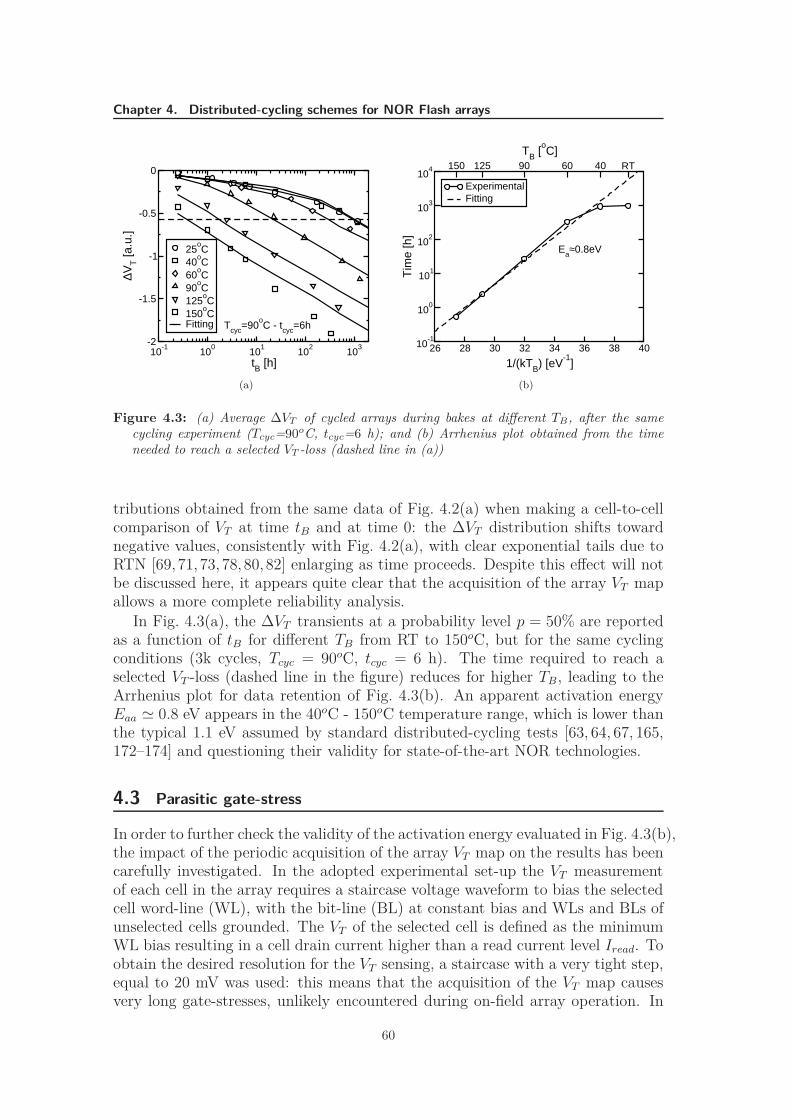
Chapter 4. Distributed-cycling schemes for NOR Flash arrays
10-1
100
101
102
103
tB [h]
-2
-1.5
-1
-0.5
0
∆VT [a
.u.]
25oC
40oC
60oC
90oC
125oC
150oC
Fitting Tcyc=90oC - tcyc=6h
(a)
26 28 30 32 34 36 38 40
1/(kTB) [eV-1
]
10-1
100
101
102
103
104
Tim
e [h
]
150 60 RT4090125TB [
oC]
ExperimentalFitting
Ea≈0.8eV
(b)
Figure 4.3: (a) Average ∆VT of cycled arrays during bakes at different TB, after the samecycling experiment (Tcyc=90oC, tcyc=6 h); and (b) Arrhenius plot obtained from the timeneeded to reach a selected VT -loss (dashed line in (a))
tributions obtained from the same data of Fig. 4.2(a) when making a cell-to-cellcomparison of VT at time tB and at time 0: the ∆VT distribution shifts towardnegative values, consistently with Fig. 4.2(a), with clear exponential tails due toRTN [69,71, 73, 78, 80, 82] enlarging as time proceeds. Despite this effect will notbe discussed here, it appears quite clear that the acquisition of the array VT mapallows a more complete reliability analysis.
In Fig. 4.3(a), the ∆VT transients at a probability level p = 50% are reportedas a function of tB for different TB from RT to 150oC, but for the same cyclingconditions (3k cycles, Tcyc = 90oC, tcyc = 6 h). The time required to reach aselected VT -loss (dashed line in the figure) reduces for higher TB, leading to theArrhenius plot for data retention of Fig. 4.3(b). An apparent activation energyEaa ≃ 0.8 eV appears in the 40oC - 150oC temperature range, which is lower thanthe typical 1.1 eV assumed by standard distributed-cycling tests [63, 64, 67, 165,172–174] and questioning their validity for state-of-the-art NOR technologies.
4.3 Parasitic gate-stress
In order to further check the validity of the activation energy evaluated in Fig. 4.3(b),the impact of the periodic acquisition of the array VT map on the results has beencarefully investigated. In the adopted experimental set-up the VT measurementof each cell in the array requires a staircase voltage waveform to bias the selectedcell word-line (WL), with the bit-line (BL) at constant bias and WLs and BLs ofunselected cells grounded. The VT of the selected cell is defined as the minimumWL bias resulting in a cell drain current higher than a read current level Iread. Toobtain the desired resolution for the VT sensing, a staircase with a very tight step,equal to 20 mV was used: this means that the acquisition of the VT map causesvery long gate-stresses, unlikely encountered during on-field array operation. In
60
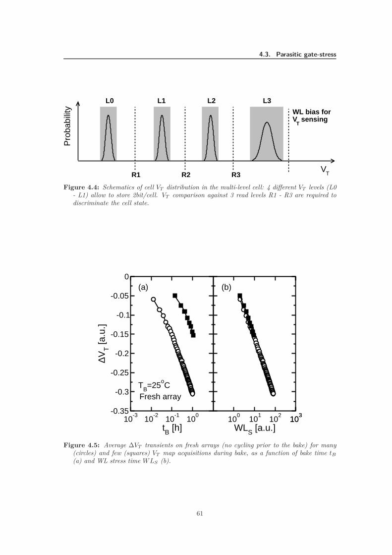
4.3. Parasitic gate-stress
VT
WL bias forV sensing
T
L3L0 L1 L2
R1 R2 R3
Pro
babi
lity
Figure 4.4: Schematics of cell VT distribution in the multi-level cell: 4 different VT levels (L0- L1) allow to store 2bit/cell. VT comparison against 3 read levels R1 - R3 are required todiscriminate the cell state.
10-3
10-2
10-1
100
tB [h]
-0.35
-0.3
-0.25
-0.2
-0.15
-0.1
-0.05
0
∆VT [a
.u.]
100
101
102
103
103
WLS [a.u.]
Fresh arrayTB=25
oC
(a) (b)
Figure 4.5: Average ∆VT transients on fresh arrays (no cycling prior to the bake) for many(circles) and few (squares) VT map acquisitions during bake, as a function of bake time tB
(a) and WL stress time WLS (b).
61
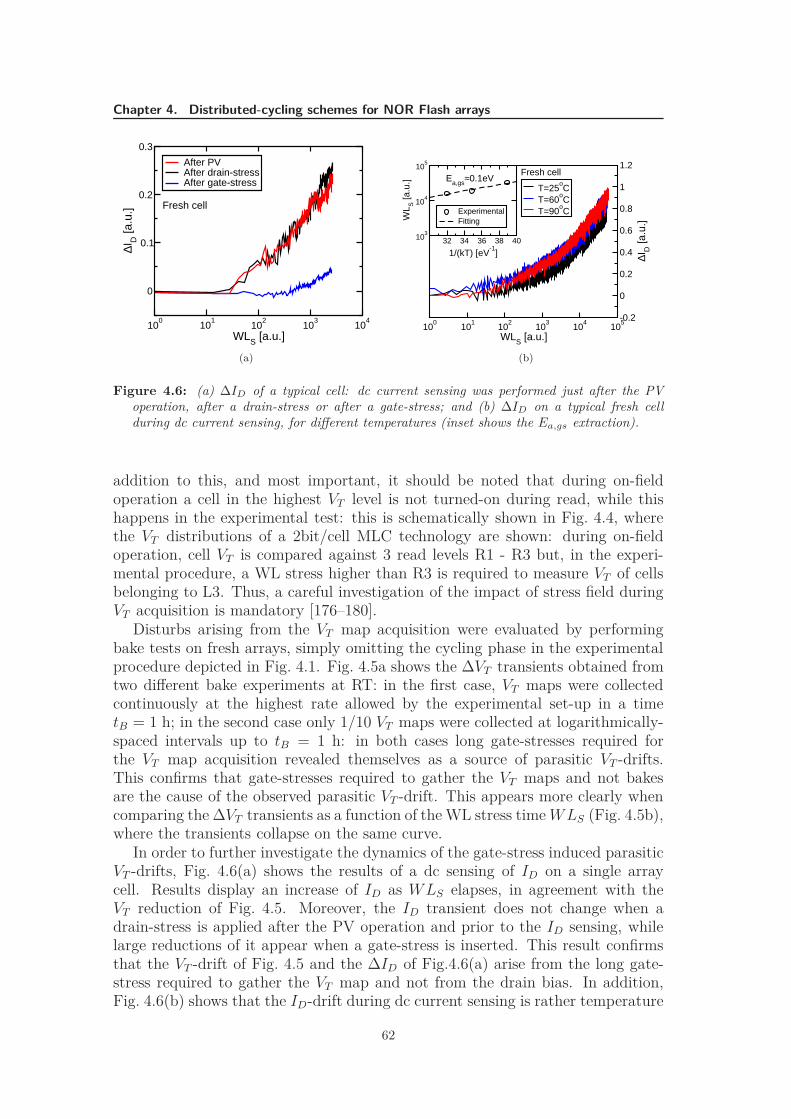
Chapter 4. Distributed-cycling schemes for NOR Flash arrays
100
101
102
103
104
WLS [a.u.]
0
0.1
0.2
0.3
∆ID [a
.u.]
After PVAfter drain-stressAfter gate-stress
Fresh cell
(a)
100
101
102
103
104
105
WLS [a.u.]
-0.2
0
0.2
0.4
0.6
0.8
1
1.2
∆ID [a
.u.]
T=25oC
T=60oC
T=90oC
32 34 36 38 40
1/(kT) [eV-1
]
103
104
105
WL S
[a.u
.]
ExperimentalFitting
Fresh cellEa,gs≈0.1eV
(b)
Figure 4.6: (a) ∆ID of a typical cell: dc current sensing was performed just after the PVoperation, after a drain-stress or after a gate-stress; and (b) ∆ID on a typical fresh cellduring dc current sensing, for different temperatures (inset shows the Ea,gs extraction).
addition to this, and most important, it should be noted that during on-fieldoperation a cell in the highest VT level is not turned-on during read, while thishappens in the experimental test: this is schematically shown in Fig. 4.4, wherethe VT distributions of a 2bit/cell MLC technology are shown: during on-fieldoperation, cell VT is compared against 3 read levels R1 - R3 but, in the experi-mental procedure, a WL stress higher than R3 is required to measure VT of cellsbelonging to L3. Thus, a careful investigation of the impact of stress field duringVT acquisition is mandatory [176–180].
Disturbs arising from the VT map acquisition were evaluated by performingbake tests on fresh arrays, simply omitting the cycling phase in the experimentalprocedure depicted in Fig. 4.1. Fig. 4.5a shows the ∆VT transients obtained fromtwo different bake experiments at RT: in the first case, VT maps were collectedcontinuously at the highest rate allowed by the experimental set-up in a timetB = 1 h; in the second case only 1/10 VT maps were collected at logarithmically-spaced intervals up to tB = 1 h: in both cases long gate-stresses required forthe VT map acquisition revealed themselves as a source of parasitic VT -drifts.This confirms that gate-stresses required to gather the VT maps and not bakesare the cause of the observed parasitic VT -drift. This appears more clearly whencomparing the ∆VT transients as a function of the WL stress timeWLS (Fig. 4.5b),where the transients collapse on the same curve.
In order to further investigate the dynamics of the gate-stress induced parasiticVT -drifts, Fig. 4.6(a) shows the results of a dc sensing of ID on a single arraycell. Results display an increase of ID as WLS elapses, in agreement with theVT reduction of Fig. 4.5. Moreover, the ID transient does not change when adrain-stress is applied after the PV operation and prior to the ID sensing, whilelarge reductions of it appear when a gate-stress is inserted. This result confirmsthat the VT -drift of Fig. 4.5 and the ∆ID of Fig.4.6(a) arise from the long gate-stress required to gather the VT map and not from the drain bias. In addition,Fig. 4.6(b) shows that the ID-drift during dc current sensing is rather temperature
62
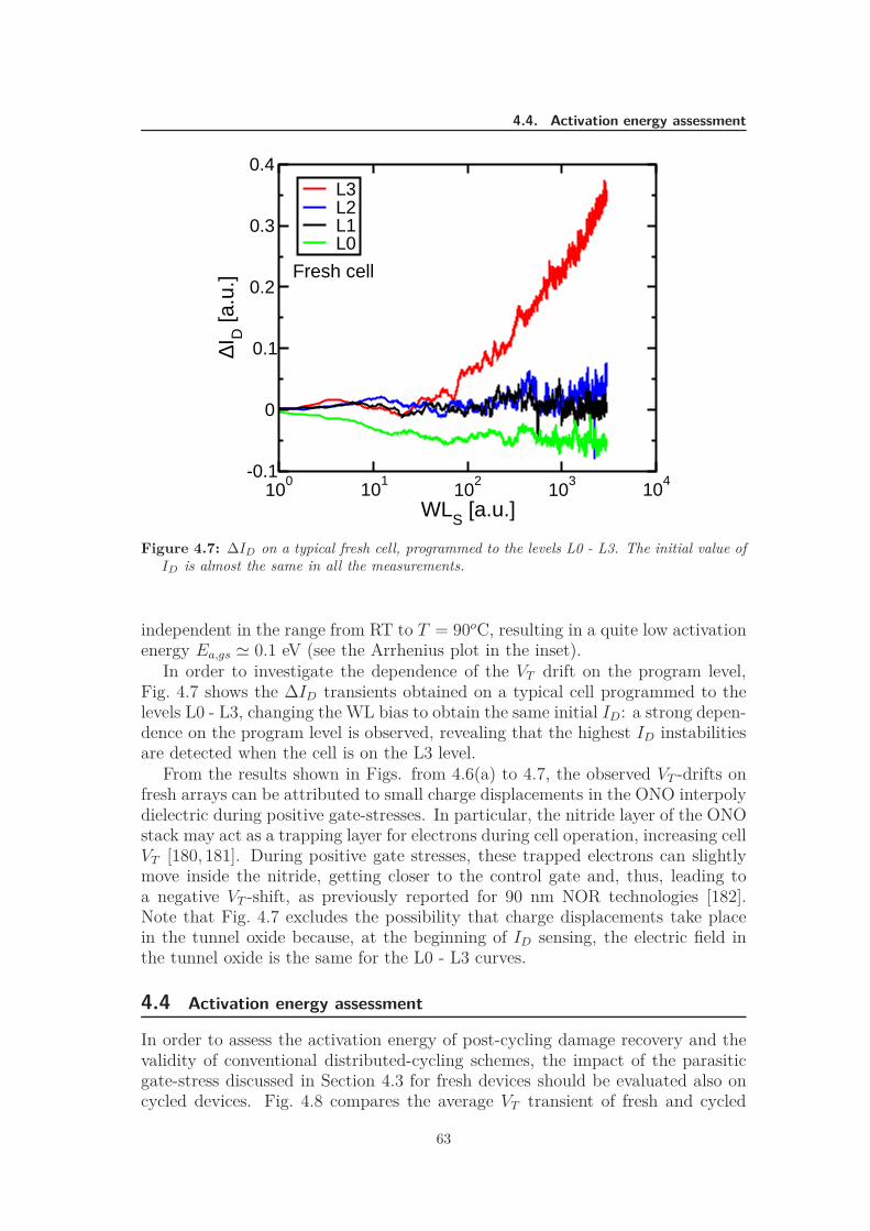
4.4. Activation energy assessment
100
101
102
103
104
WLS [a.u.]
-0.1
0
0.1
0.2
0.3
0.4
∆ID [a
.u.]
L3L2L1L0
Fresh cell
Figure 4.7: ∆ID on a typical fresh cell, programmed to the levels L0 - L3. The initial value ofID is almost the same in all the measurements.
independent in the range from RT to T = 90oC, resulting in a quite low activationenergy Ea,gs ≃ 0.1 eV (see the Arrhenius plot in the inset).
In order to investigate the dependence of the VT drift on the program level,Fig. 4.7 shows the ∆ID transients obtained on a typical cell programmed to thelevels L0 - L3, changing the WL bias to obtain the same initial ID: a strong depen-dence on the program level is observed, revealing that the highest ID instabilitiesare detected when the cell is on the L3 level.
From the results shown in Figs. from 4.6(a) to 4.7, the observed VT -drifts onfresh arrays can be attributed to small charge displacements in the ONO interpolydielectric during positive gate-stresses. In particular, the nitride layer of the ONOstack may act as a trapping layer for electrons during cell operation, increasing cellVT [180, 181]. During positive gate stresses, these trapped electrons can slightlymove inside the nitride, getting closer to the control gate and, thus, leading toa negative VT -shift, as previously reported for 90 nm NOR technologies [182].Note that Fig. 4.7 excludes the possibility that charge displacements take placein the tunnel oxide because, at the beginning of ID sensing, the electric field inthe tunnel oxide is the same for the L0 - L3 curves.
4.4 Activation energy assessment
In order to assess the activation energy of post-cycling damage recovery and thevalidity of conventional distributed-cycling schemes, the impact of the parasiticgate-stress discussed in Section 4.3 for fresh devices should be evaluated also oncycled devices. Fig. 4.8 compares the average VT transient of fresh and cycled
63
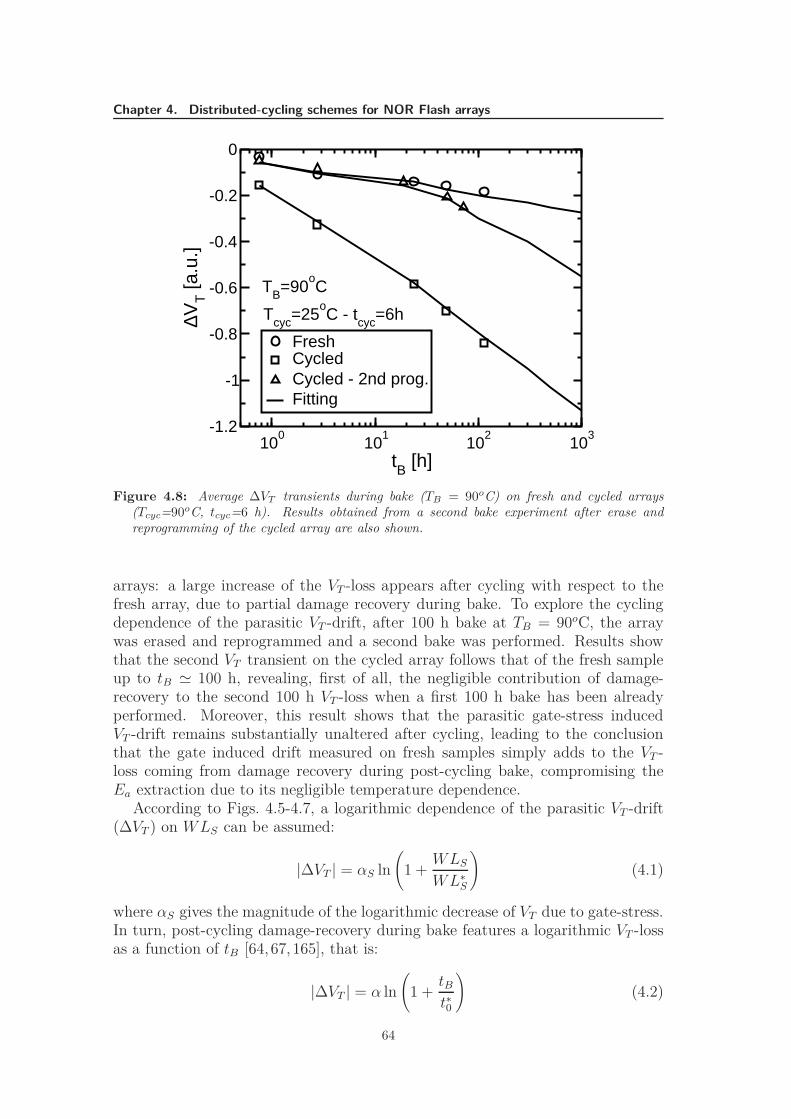
Chapter 4. Distributed-cycling schemes for NOR Flash arrays
100
101
102
103
tB [h]
-1.2
-1
-0.8
-0.6
-0.4
-0.2
0
∆VT [a
.u.]
FreshCycledCycled - 2nd prog.Fitting
TB=90oC
Tcyc=25oC - tcyc=6h
Figure 4.8: Average ∆VT transients during bake (TB = 90oC) on fresh and cycled arrays(Tcyc=90oC, tcyc=6 h). Results obtained from a second bake experiment after erase andreprogramming of the cycled array are also shown.
arrays: a large increase of the VT -loss appears after cycling with respect to thefresh array, due to partial damage recovery during bake. To explore the cyclingdependence of the parasitic VT -drift, after 100 h bake at TB = 90oC, the arraywas erased and reprogrammed and a second bake was performed. Results showthat the second VT transient on the cycled array follows that of the fresh sampleup to tB ≃ 100 h, revealing, first of all, the negligible contribution of damage-recovery to the second 100 h VT -loss when a first 100 h bake has been alreadyperformed. Moreover, this result shows that the parasitic gate-stress inducedVT -drift remains substantially unaltered after cycling, leading to the conclusionthat the gate induced drift measured on fresh samples simply adds to the VT -loss coming from damage recovery during post-cycling bake, compromising theEa extraction due to its negligible temperature dependence.
According to Figs. 4.5-4.7, a logarithmic dependence of the parasitic VT -drift(∆VT ) on WLS can be assumed:
|∆VT | = αS ln
(
1 +WLS
WL∗
S
)
(4.1)
where αS gives the magnitude of the logarithmic decrease of VT due to gate-stress.In turn, post-cycling damage-recovery during bake features a logarithmic VT -lossas a function of tB [64, 67, 165], that is:
|∆VT | = α ln
(
1 +tBt∗0
)
(4.2)
64
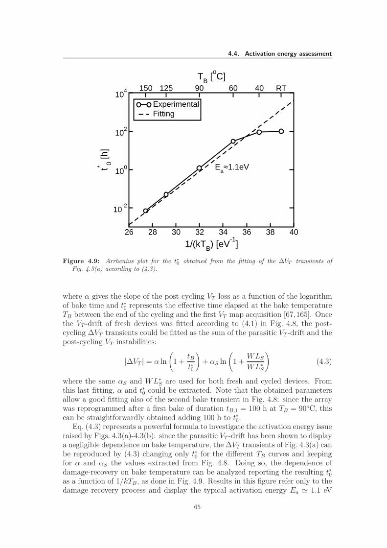
4.4. Activation energy assessment
26 28 30 32 34 36 38 40
1/(kTB) [eV-1
]
10-2
100
102
104
t* 0 [h]
150 60 RT4090125TB [
oC]
ExperimentalFitting
Ea≈1.1eV
Figure 4.9: Arrhenius plot for the t∗
0 obtained from the fitting of the ∆VT transients ofFig. 4.3(a) according to (4.3).
where α gives the slope of the post-cycling VT -loss as a function of the logarithmof bake time and t∗0 represents the effective time elapsed at the bake temperatureTB between the end of the cycling and the first VT map acquisition [67,165]. Oncethe VT -drift of fresh devices was fitted according to (4.1) in Fig. 4.8, the post-cycling ∆VT transients could be fitted as the sum of the parasitic VT -drift and thepost-cycling VT instabilities:
|∆VT | = α ln
(
1 +tBt∗0
)
+ αS ln
(
1 +WLS
WL∗
S
)
(4.3)
where the same αS and WL∗
S are used for both fresh and cycled devices. Fromthis last fitting, α and t∗0 could be extracted. Note that the obtained parametersallow a good fitting also of the second bake transient in Fig. 4.8: since the arraywas reprogrammed after a first bake of duration tB,1 = 100 h at TB = 90oC, thiscan be straightforwardly obtained adding 100 h to t∗0.
Eq. (4.3) represents a powerful formula to investigate the activation energy issueraised by Figs. 4.3(a)-4.3(b): since the parasitic VT -drift has been shown to displaya negligible dependence on bake temperature, the ∆VT transients of Fig. 4.3(a) canbe reproduced by (4.3) changing only t∗0 for the different TB curves and keepingfor α and αS the values extracted from Fig. 4.8. Doing so, the dependence ofdamage-recovery on bake temperature can be analyzed reporting the resulting t∗0as a function of 1/kTB, as done in Fig. 4.9. Results in this figure refer only to thedamage recovery process and display the typical activation energy Ea ≃ 1.1 eV
65
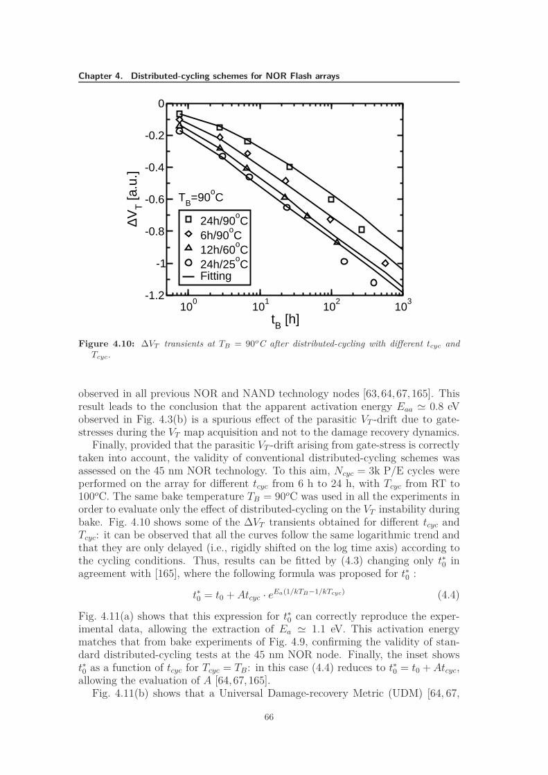
Chapter 4. Distributed-cycling schemes for NOR Flash arrays
100
101
102
103
tB [h]
-1.2
-1
-0.8
-0.6
-0.4
-0.2
0
∆VT [a
.u.]
24h/90oC
6h/90oC
12h/60oC
24h/25oC
Fitting
TB=90oC
Figure 4.10: ∆VT transients at TB = 90oC after distributed-cycling with different tcyc andTcyc.
observed in all previous NOR and NAND technology nodes [63, 64, 67, 165]. Thisresult leads to the conclusion that the apparent activation energy Eaa ≃ 0.8 eVobserved in Fig. 4.3(b) is a spurious effect of the parasitic VT -drift due to gate-stresses during the VT map acquisition and not to the damage recovery dynamics.
Finally, provided that the parasitic VT -drift arising from gate-stress is correctlytaken into account, the validity of conventional distributed-cycling schemes wasassessed on the 45 nm NOR technology. To this aim, Ncyc = 3k P/E cycles wereperformed on the array for different tcyc from 6 h to 24 h, with Tcyc from RT to100oC. The same bake temperature TB = 90oC was used in all the experiments inorder to evaluate only the effect of distributed-cycling on the VT instability duringbake. Fig. 4.10 shows some of the ∆VT transients obtained for different tcyc andTcyc: it can be observed that all the curves follow the same logarithmic trend andthat they are only delayed (i.e., rigidly shifted on the log time axis) according tothe cycling conditions. Thus, results can be fitted by (4.3) changing only t∗0 inagreement with [165], where the following formula was proposed for t∗0 :
t∗0 = t0 + Atcyc · eEa(1/kTB−1/kTcyc) (4.4)
Fig. 4.11(a) shows that this expression for t∗0 can correctly reproduce the exper-imental data, allowing the extraction of Ea ≃ 1.1 eV. This activation energymatches that from bake experiments of Fig. 4.9, confirming the validity of stan-dard distributed-cycling tests at the 45 nm NOR node. Finally, the inset showst∗0 as a function of tcyc for Tcyc = TB: in this case (4.4) reduces to t∗0 = t0 + Atcyc,allowing the evaluation of A [64, 67, 165].
Fig. 4.11(b) shows that a Universal Damage-recovery Metric (UDM) [64, 67,
66
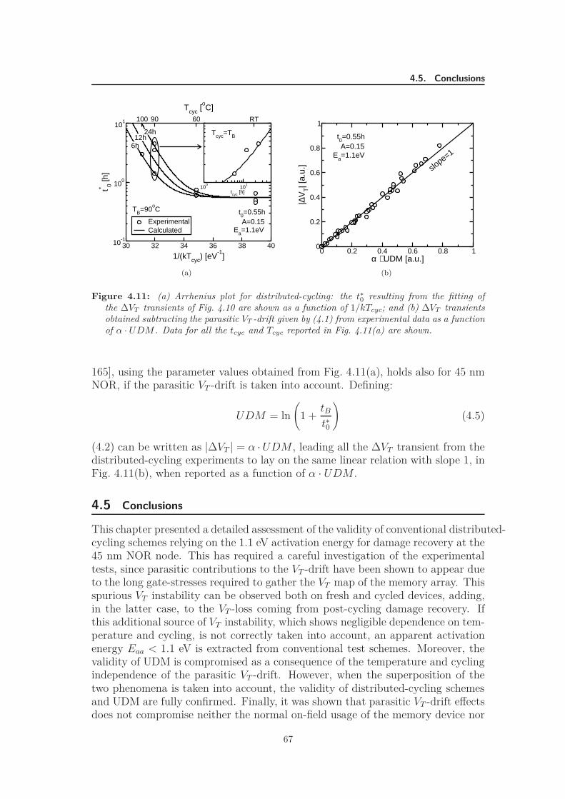
4.5. Conclusions
30 32 34 36 38 40
1/(kTcyc) [eV-1
]
10-1
100
101
t* 0 [h]
90 60 RT100
Tcyc [oC]
ExperimentalCalculated
100
101
tcyc [h]
t0=0.55hA=0.15
Ea=1.1eV
6h12h
24h Tcyc=TB
TB=90oC
(a)
0 0.2 0.4 0.6 0.8 1α ⋅ UDM [a.u.]
0
0.2
0.4
0.6
0.8
1
|∆V
T| [
a.u.
]
t0=0.55h
slope=1Ea=1.1eV
A=0.15
(b)
Figure 4.11: (a) Arrhenius plot for distributed-cycling: the t∗
0 resulting from the fitting ofthe ∆VT transients of Fig. 4.10 are shown as a function of 1/kTcyc; and (b) ∆VT transientsobtained subtracting the parasitic VT -drift given by (4.1) from experimental data as a functionof α · UDM . Data for all the tcyc and Tcyc reported in Fig. 4.11(a) are shown.
165], using the parameter values obtained from Fig. 4.11(a), holds also for 45 nmNOR, if the parasitic VT -drift is taken into account. Defining:
UDM = ln
(
1 +tBt∗0
)
(4.5)
(4.2) can be written as |∆VT | = α ·UDM , leading all the ∆VT transient from thedistributed-cycling experiments to lay on the same linear relation with slope 1, inFig. 4.11(b), when reported as a function of α · UDM .
4.5 Conclusions
This chapter presented a detailed assessment of the validity of conventional distributed-cycling schemes relying on the 1.1 eV activation energy for damage recovery at the45 nm NOR node. This has required a careful investigation of the experimentaltests, since parasitic contributions to the VT -drift have been shown to appear dueto the long gate-stresses required to gather the VT map of the memory array. Thisspurious VT instability can be observed both on fresh and cycled devices, adding,in the latter case, to the VT -loss coming from post-cycling damage recovery. Ifthis additional source of VT instability, which shows negligible dependence on tem-perature and cycling, is not correctly taken into account, an apparent activationenergy Eaa < 1.1 eV is extracted from conventional test schemes. Moreover, thevalidity of UDM is compromised as a consequence of the temperature and cyclingindependence of the parasitic VT -drift. However, when the superposition of thetwo phenomena is taken into account, the validity of distributed-cycling schemesand UDM are fully confirmed. Finally, it was shown that parasitic VT -drift effectsdoes not compromise neither the normal on-field usage of the memory device nor
67
Chapter 4. Distributed-cycling schemes for NOR Flash arrays
the coverage of JEDEC JESD47’s HTDR and LTDR qualification tests [173,174],since they come into play only when longer stress times and higher voltages thennormal on-field operation are adopted, as in case the adopted experimental pro-cedure.
68
CHAPTER5
Fundamental variability sources in Flash memories
This chapter discusses the impact of fundamental variability sources on sub-100 nm NAND Flash memories operation; in particular, the atomistic na-ture of the substrate doping and the discrete nature of the electrons flow
into the floating-gate have been previously reported as fundamental phenomena,affecting the statistical dispersion of neutral cell threshold voltage and program-ming accuracy, respectively. This chapter investigates the impact of control-gateand floating-gate doping and geometry on the electron-injection spread of na-noscale NAND Flash memories, addressing the electron-injection spread scalingtrend. Then, the attention is focused on data retention, presenting a comparisonof the dispersion contribution due to the neutral threshold-voltage spread and theelectron-emission statistics from the floating gate, evaluating their effect on thedata retention transients of a memory array. Finally, the first array-level exper-imental observation of post-cycling discrete electron detrapping from the tunneloxide in sub-30nm NAND Flash arrays is given, providing an accurate stochasticmodel of cycled array data retention.
5.1 Introduction
Variability effects are becoming more and more important for NAND Flash mem-ories, affecting the uniformity and reproducibility of device characteristics andoperations as cell dimensions scale down [107, 151, 183, 184]. In this respect, twomain classes of variability sources can be identified: the first one is related tocell-to-cell parameter variations, due to process tolerances or fundamental rea-sons [107]; the second one accounts for the statistics of few-electron phenomenaand it is related to the discrete electron transfer to/from the floating gate (FG)
69
Chapter 5. Fundamental variability sources in Flash memories
during cell operation [151,183,184]. In particular, the statistical injection of elec-trons into the floating gate (FG) has been recently shown to set the ultimate limitto the accuracy of the incremental step pulse programming (ISPP) algorithm fordeca-nanometer NAND Flash memories [151, 184–186]. Scaling of device dimen-sions results, in fact, into a continuous decrease of the FG charge controlling cellstate, making the fundamental fluctuation of the number of electrons transferredto the FG during ISPP more and more important for the programmed thresholdvoltage (VT ) distribution of the array. While this latter variability source appearsonly when the charge state of the FG is changed, fluctuations in cell parametersalso result into a spread of the neutral threshold voltage (VT,0) of the cells in thememory array [107].
This chapter firstly investigate the impact of CG and FG design on the electron-injection spread (EIS) of deca-nanometer NAND Flash memories, not only interms of their geometry but also of their doping, which is becoming more and moreimportant for device operation [187]; then, a comparison of cell-to-cell parametervariations and of electron-emission statistics (EES) on the retention character-istics of nanoscale NAND Flash memories is presented. Referring to fresh cellsprogrammed to the same threshold voltage (VT ) level, both the VT,0 spread andEES are shown to represent a source of statistical variability for data retention, re-sulting into a broadening of the array VT distribution as retention time elapses. Aquantitative assessment of the two contributions clearly shows, however, that theVT,0 spread, and therefore cell-to-cell parameter variations, dominates over theEES spread for data retention variability of nanoscale NAND Flash memories.Finally, a statistical analysis of post-cycling data retention is presented, showingby means of experimental and modeling analysis that discrete electron detrappingfrom tunnel oxide rules data retention on sub-30 nm NAND Flash arrays and thatdetrapping statistics is a major post-cycling spread source on aggressively scaledarrays.
5.2 Fundamental variability sources
5.2.1 Neutral cell threshold voltage spread
As a consequence of the high integration density which can be achieved in nano-scale Flash memory devices, variability has emerged as a major issue for arrayoperation and reliability. The continuous shrinking of the cell size, up to de-cananometer scale, has been largely increasing the variability sources (e.g., dueto cell-to-cell parameter variations), setting new constraints to array functional-ity. In the case of Flash memories, an accurate control of cell VT is required inorder to guarantee the desired functionality: the variability sources result, firstof all, in a statistical variation of the neutral cell threshold voltage (VT,0) [107];Fig. 5.1(a) shows the VT,0 spread as a function of the technology node, highlight-ing how the variability effects get more severe with the technology scaling. Themajor variability sources that contributes to VT,0 spread are individually shownin Fig. 5.1(b): besides process-induced tolerances (e.g., cell length/width fluctua-tions) and VT,0 variations due to oxide traps fluctuations (OTF), random dopantfluctuations (RDF) are predicted to play a major role in sub-30 nm technologies.
70
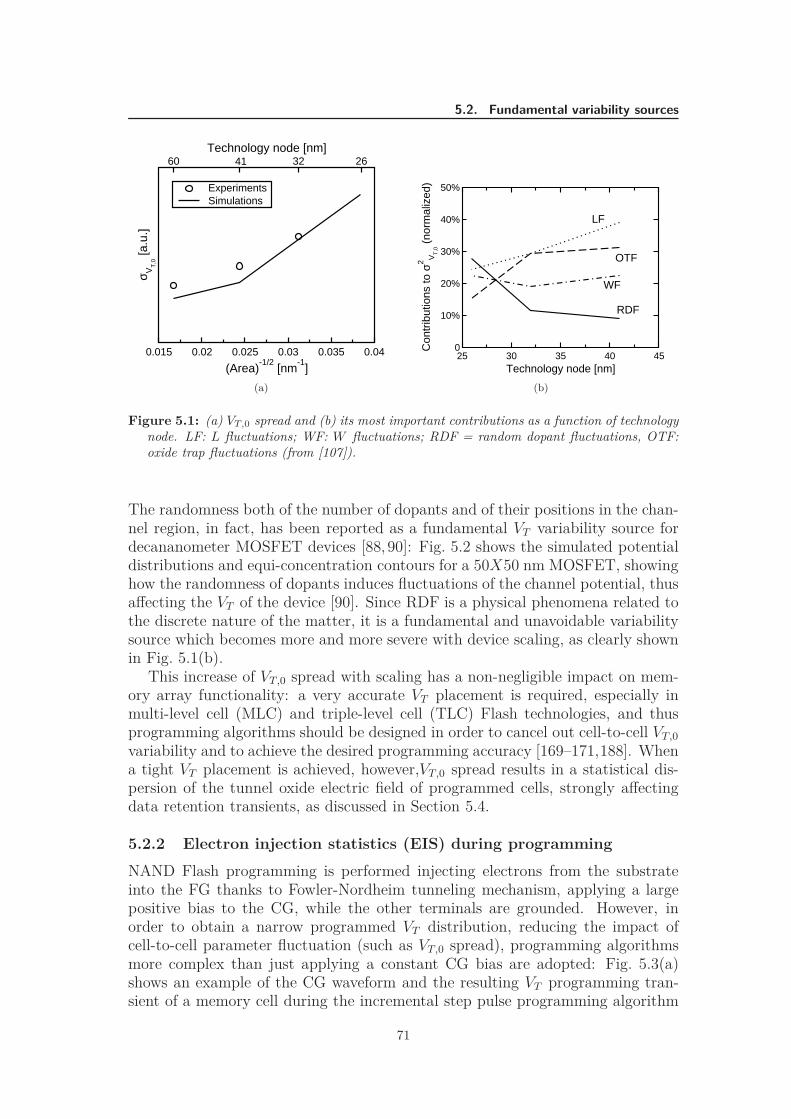
5.2. Fundamental variability sources
0.015 0.02 0.025 0.03 0.035 0.04
(Area)-1/2
[nm-1
]
σ VT
,0 [a
.u.]
60 41 32 26Technology node [nm]
ExperimentsSimulations
(a)
25 30 35 40 45Technology node [nm]
0
10%
20%
30%
40%
50%
Con
trib
utio
ns to
σ2 V
T,0 (
norm
aliz
ed)
RDF
WF
OTF
LF
(b)
Figure 5.1: (a) VT,0 spread and (b) its most important contributions as a function of technologynode. LF: L fluctuations; WF: W fluctuations; RDF = random dopant fluctuations, OTF:oxide trap fluctuations (from [107]).
The randomness both of the number of dopants and of their positions in the chan-nel region, in fact, has been reported as a fundamental VT variability source fordecananometer MOSFET devices [88, 90]: Fig. 5.2 shows the simulated potentialdistributions and equi-concentration contours for a 50X50 nm MOSFET, showinghow the randomness of dopants induces fluctuations of the channel potential, thusaffecting the VT of the device [90]. Since RDF is a physical phenomena related tothe discrete nature of the matter, it is a fundamental and unavoidable variabilitysource which becomes more and more severe with device scaling, as clearly shownin Fig. 5.1(b).
This increase of VT,0 spread with scaling has a non-negligible impact on mem-ory array functionality: a very accurate VT placement is required, especially inmulti-level cell (MLC) and triple-level cell (TLC) Flash technologies, and thusprogramming algorithms should be designed in order to cancel out cell-to-cell VT,0
variability and to achieve the desired programming accuracy [169–171,188]. Whena tight VT placement is achieved, however,VT,0 spread results in a statistical dis-persion of the tunnel oxide electric field of programmed cells, strongly affectingdata retention transients, as discussed in Section 5.4.
5.2.2 Electron injection statistics (EIS) during programming
NAND Flash programming is performed injecting electrons from the substrateinto the FG thanks to Fowler-Nordheim tunneling mechanism, applying a largepositive bias to the CG, while the other terminals are grounded. However, inorder to obtain a narrow programmed VT distribution, reducing the impact ofcell-to-cell parameter fluctuation (such as VT,0 spread), programming algorithmsmore complex than just applying a constant CG bias are adopted: Fig. 5.3(a)shows an example of the CG waveform and the resulting VT programming tran-sient of a memory cell during the incremental step pulse programming algorithm
71
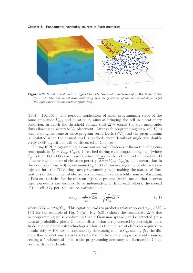
Chapter 5. Fundamental variability sources in Flash memories
Figure 5.2: Simulation domain in typical Density Gradient simulations of a 50X50 nm MOS-FET. (a) Potential distribution indicating also the positions of the individual dopants.(b)One equi-concentration contour (from [90]).
(ISSP) [150, 151]. The periodic application of small programming steps of thesame amplitude Vstep and duration τs aims at bringing the cell in a stationarycondition, in which the threshold voltage shift ∆VT equals the step amplitude,thus allowing an accurate VT placement. After each programming step, cell VT iscompared against one or more program verify levels (PVs) and the programmingis inhibited when the desired level is reached: more details of single and doubleverify ISSP algorithms will be discussed in Chapter 6.
During ISPP programming, a constant average Fowler-Nordheim tunneling cur-rent equals to IG = Vstep ·Cpp/τs is reached during each programming step (whereCpp is the CG to FG capacitance), which corresponds to the injection into the FGof an average number of electrons per step ∆n = Vstep ·Cpp/q. This means that inthe example of Fig. 5.3(a), assuming Cpp ≃ 30 aF, on average only 50 electrons areinjected into the FG during each programming step, making the statistical fluc-tuations of the number of electrons a non-negligible variability source. Assuminga Poisson statistics for the electron injection process (which means that electroninjection events are assumed to be independent on from each other), the spreadof the cell ∆VT per step can be evaluated as:
σ∆VT=
q
Cpp
√
∆n =
√
q
Cpp∆VT , (5.1)
where ∆VT = q∆n/Cpp. This equation leads to predict a relative spread σ∆VT/∆VT =
13% for the example of Fig. 5.3(a). Fig. 5.3(b) shows the cumulative ∆VT dueto programming pulse confirming that a Gaussian spread can be detected (in anormal probability plot a Gaussian distribution is represented by a straight line).In decananometer Flash technologies, thus, as the number of electrons required toobtain ∆VT = 100 mV is continuously decreasing due to Cpp scaling [5], the dis-crete flow of electrons transferred into the FG become a major variability source,setting a fundamental limit to the programming accuracy, as discussed in Chap-ter 6 with more details.
72
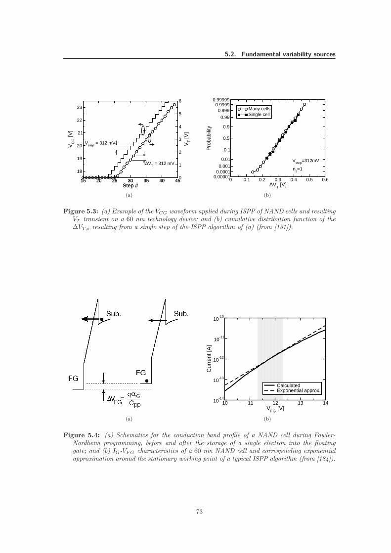
5.2. Fundamental variability sources
15 20 25 30 35 40 45Step #
0
1
2
3
4
5
6
VT [V
]15 20 25 30 35 40 45
Step #
18
19
20
21
22
23
VC
G [V
]
Vstep = 312 mV
∆VT = 312 mV
(a)
0 0.1 0.2 0.3 0.4 0.5 0.6∆VT [V]
0.000010.00010.001
0.01
0.1
0.5
0.9
0.99
0.9990.9999
0.99999
Pro
babi
lity
Many cellsSingle cell
ns=1
Vstep=312mV
(b)
Figure 5.3: (a) Example of the VCG waveform applied during ISPP of NAND cells and resultingVT transient on a 60 nm technology device; and (b) cumulative distribution function of the∆VT,s resulting from a single step of the ISPP algorithm of (a) (from [151]).
(a)
10 11 12 13 14VFG [V]
10-14
10-13
10-12
10-11
10-10
Cur
rent
[A]
CalculatedExponential approx.
(b)
Figure 5.4: (a) Schematics for the conduction band profile of a NAND cell during Fowler-Nordheim programming, before and after the storage of a single electron into the floatinggate; and (b) IG-VF G characteristics of a 60 nm NAND cell and corresponding exponentialapproximation around the stationary working point of a typical ISPP algorithm (from [184]).
73
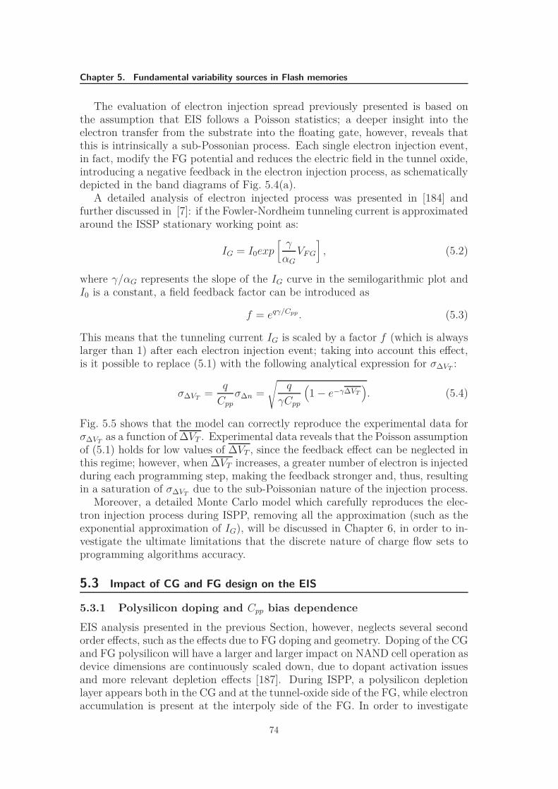
Chapter 5. Fundamental variability sources in Flash memories
The evaluation of electron injection spread previously presented is based onthe assumption that EIS follows a Poisson statistics; a deeper insight into theelectron transfer from the substrate into the floating gate, however, reveals thatthis is intrinsically a sub-Possonian process. Each single electron injection event,in fact, modify the FG potential and reduces the electric field in the tunnel oxide,introducing a negative feedback in the electron injection process, as schematicallydepicted in the band diagrams of Fig. 5.4(a).
A detailed analysis of electron injected process was presented in [184] andfurther discussed in [7]: if the Fowler-Nordheim tunneling current is approximatedaround the ISSP stationary working point as:
IG = I0exp[
γ
αG
VF G
]
, (5.2)
where γ/αG represents the slope of the IG curve in the semilogarithmic plot andI0 is a constant, a field feedback factor can be introduced as
f = eqγ/Cpp . (5.3)
This means that the tunneling current IG is scaled by a factor f (which is alwayslarger than 1) after each electron injection event; taking into account this effect,is it possible to replace (5.1) with the following analytical expression for σ∆VT
:
σ∆VT=
q
Cppσ∆n =
√
q
γCpp
(
1 − e−γ∆VT
)
. (5.4)
Fig. 5.5 shows that the model can correctly reproduce the experimental data forσ∆VT
as a function of ∆VT . Experimental data reveals that the Poisson assumptionof (5.1) holds for low values of ∆VT , since the feedback effect can be neglected inthis regime; however, when ∆VT increases, a greater number of electron is injectedduring each programming step, making the feedback stronger and, thus, resultingin a saturation of σ∆VT
due to the sub-Poissonian nature of the injection process.Moreover, a detailed Monte Carlo model which carefully reproduces the elec-
tron injection process during ISPP, removing all the approximation (such as theexponential approximation of IG), will be discussed in Chapter 6, in order to in-vestigate the ultimate limitations that the discrete nature of charge flow sets toprogramming algorithms accuracy.
5.3 Impact of CG and FG design on the EIS
5.3.1 Polysilicon doping and Cpp bias dependence
EIS analysis presented in the previous Section, however, neglects several secondorder effects, such as the effects due to FG doping and geometry. Doping of the CGand FG polysilicon will have a larger and larger impact on NAND cell operation asdevice dimensions are continuously scaled down, due to dopant activation issuesand more relevant depletion effects [187]. During ISPP, a polysilicon depletionlayer appears both in the CG and at the tunnel-oxide side of the FG, while electronaccumulation is present at the interpoly side of the FG. In order to investigate
74
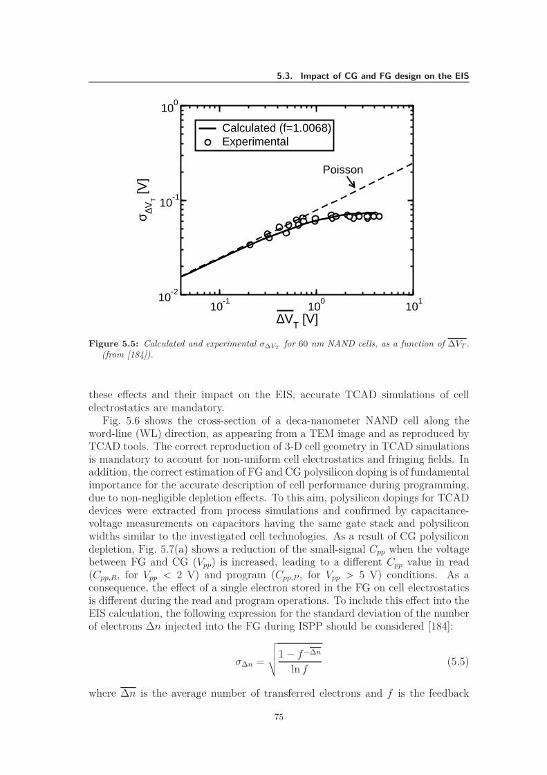
5.3. Impact of CG and FG design on the EIS
10-1
100
101
∆VT [V]
10-2
10-1
100
σ ∆VT [V
]Calculated (f=1.0068)Experimental
Poisson
Figure 5.5: Calculated and experimental σ∆VTfor 60 nm NAND cells, as a function of ∆VT .
(from [184]).
these effects and their impact on the EIS, accurate TCAD simulations of cellelectrostatics are mandatory.
Fig. 5.6 shows the cross-section of a deca-nanometer NAND cell along theword-line (WL) direction, as appearing from a TEM image and as reproduced byTCAD tools. The correct reproduction of 3-D cell geometry in TCAD simulationsis mandatory to account for non-uniform cell electrostatics and fringing fields. Inaddition, the correct estimation of FG and CG polysilicon doping is of fundamentalimportance for the accurate description of cell performance during programming,due to non-negligible depletion effects. To this aim, polysilicon dopings for TCADdevices were extracted from process simulations and confirmed by capacitance-voltage measurements on capacitors having the same gate stack and polysiliconwidths similar to the investigated cell technologies. As a result of CG polysilicondepletion, Fig. 5.7(a) shows a reduction of the small-signal Cpp when the voltagebetween FG and CG (Vpp) is increased, leading to a different Cpp value in read(Cpp,R, for Vpp < 2 V) and program (Cpp,P , for Vpp > 5 V) conditions. As aconsequence, the effect of a single electron stored in the FG on cell electrostaticsis different during the read and program operations. To include this effect into theEIS calculation, the following expression for the standard deviation of the numberof electrons ∆n injected into the FG during ISPP should be considered [184]:
σ∆n =
√
√
√
√
1 − f−∆n
ln f(5.5)
where ∆n is the average number of transferred electrons and f is the feedback
75
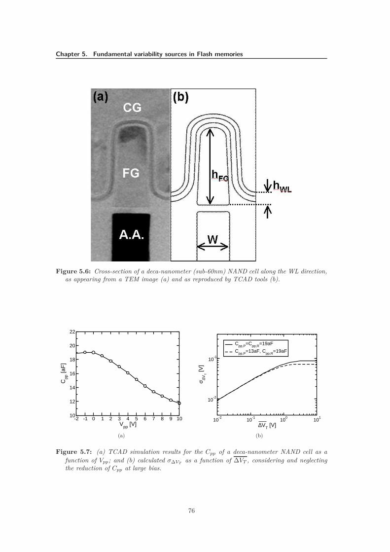
Chapter 5. Fundamental variability sources in Flash memories
Figure 5.6: Cross-section of a deca-nanometer (sub-60nm) NAND cell along the WL direction,as appearing from a TEM image (a) and as reproduced by TCAD tools (b).
-2 -1 0 1 2 3 4 5 6 7 8 9 10Vpp [V]
10
12
14
16
18
20
22
Cpp
[aF
]
(a)
10-2
10-1
100
101
∆VT [V]
10-2
10-1
σ ∆VT [V
]
Cpp,P=Cpp,R=19aF
Cpp,P=13aF, Cpp,R=19aF
(b)
Figure 5.7: (a) TCAD simulation results for the Cpp of a deca-nanometer NAND cell as a
function of Vpp; and (b) calculated σ∆VTas a function of ∆VT , considering and neglecting
the reduction of Cpp at large bias.
76
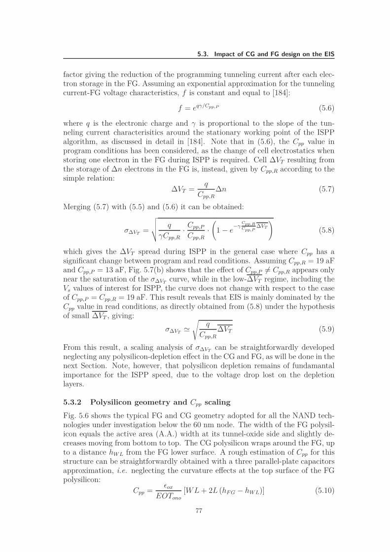
5.3. Impact of CG and FG design on the EIS
factor giving the reduction of the programming tunneling current after each elec-tron storage in the FG. Assuming an exponential approximation for the tunnelingcurrent-FG voltage characteristics, f is constant and equal to [184]:
f = eqγ/Cpp,P (5.6)
where q is the electronic charge and γ is proportional to the slope of the tun-neling current characterisitics around the stationary working point of the ISPPalgorithm, as discussed in detail in [184]. Note that in (5.6), the Cpp value inprogram conditions has been considered, as the change of cell electrostatics whenstoring one electron in the FG during ISPP is required. Cell ∆VT resulting fromthe storage of ∆n electrons in the FG is, instead, given by Cpp,R according to thesimple relation:
∆VT =q
Cpp,R∆n (5.7)
Merging (5.7) with (5.5) and (5.6) it can be obtained:
σ∆VT=
√
√
√
√
q
γCpp,R· Cpp,P
Cpp,R·(
1 − e−γ
Cpp,R
Cpp,P∆VT
)
(5.8)
which gives the ∆VT spread during ISPP in the general case where Cpp has asignificant change between program and read conditions. Assuming Cpp,R = 19 aFand Cpp,P = 13 aF, Fig. 5.7(b) shows that the effect of Cpp,P 6= Cpp,R appears onlynear the saturation of the σ∆VT
curve, while in the low-∆VT regime, including theVs values of interest for ISPP, the curve does not change with respect to the caseof Cpp,P = Cpp,R = 19 aF. This result reveals that EIS is mainly dominated by theCpp value in read conditions, as directly obtained from (5.8) under the hypothesisof small ∆VT , giving:
σ∆VT≃√
q
Cpp,R
∆VT (5.9)
From this result, a scaling analysis of σ∆VTcan be straightforwardly developed
neglecting any polysilicon-depletion effect in the CG and FG, as will be done in thenext Section. Note, however, that polysilicon depletion remains of fundamantalimportance for the ISPP speed, due to the voltage drop lost on the depletionlayers.
5.3.2 Polysilicon geometry and Cpp scaling
Fig. 5.6 shows the typical FG and CG geometry adopted for all the NAND tech-nologies under investigation below the 60 nm node. The width of the FG polysil-icon equals the active area (A.A.) width at its tunnel-oxide side and slightly de-creases moving from bottom to top. The CG polysilicon wraps around the FG, upto a distance hW L from the FG lower surface. A rough estimation of Cpp for thisstructure can be straightforwardly obtained with a three parallel-plate capacitorsapproximation, i.e. neglecting the curvature effects at the top surface of the FGpolysilicon:
Cpp =ǫox
EOTono
[WL+ 2L (hF G − hW L)] (5.10)
77
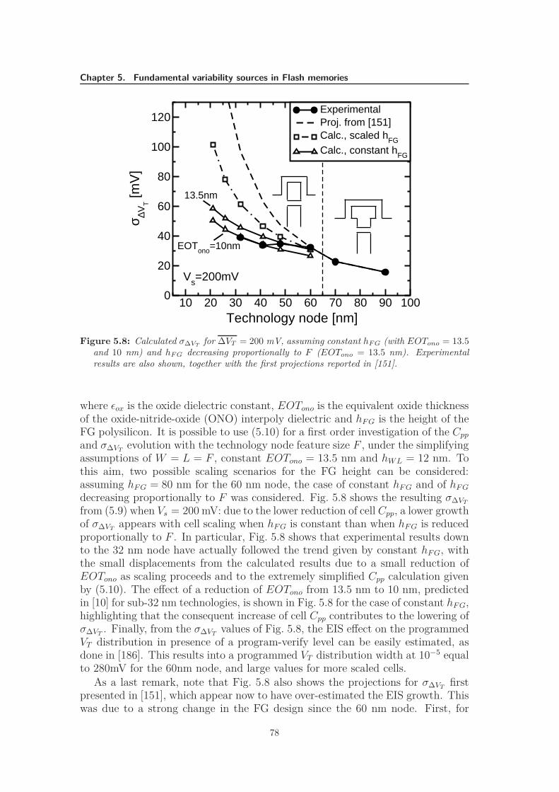
Chapter 5. Fundamental variability sources in Flash memories
10 20 30 40 50 60 70 80 90 100Technology node [nm]
0
20
40
60
80
100
120
σ ∆VT [m
V]
ExperimentalProj. from [151]Calc., scaled hFG
Calc., constant hFG
Vs=200mV
EOTono=10nm
13.5nm
Figure 5.8: Calculated σ∆VTfor ∆VT = 200 mV, assuming constant hF G (with EOTono = 13.5
and 10 nm) and hF G decreasing proportionally to F (EOTono = 13.5 nm). Experimentalresults are also shown, together with the first projections reported in [151].
where ǫox is the oxide dielectric constant, EOTono is the equivalent oxide thicknessof the oxide-nitride-oxide (ONO) interpoly dielectric and hF G is the height of theFG polysilicon. It is possible to use (5.10) for a first order investigation of the Cpp
and σ∆VTevolution with the technology node feature size F , under the simplifying
assumptions of W = L = F , constant EOTono = 13.5 nm and hW L = 12 nm. Tothis aim, two possible scaling scenarios for the FG height can be considered:assuming hF G = 80 nm for the 60 nm node, the case of constant hF G and of hF G
decreasing proportionally to F was considered. Fig. 5.8 shows the resulting σ∆VT
from (5.9) when Vs = 200 mV: due to the lower reduction of cell Cpp, a lower growthof σ∆VT
appears with cell scaling when hF G is constant than when hF G is reducedproportionally to F . In particular, Fig. 5.8 shows that experimental results downto the 32 nm node have actually followed the trend given by constant hF G, withthe small displacements from the calculated results due to a small reduction ofEOTono as scaling proceeds and to the extremely simplified Cpp calculation givenby (5.10). The effect of a reduction of EOTono from 13.5 nm to 10 nm, predictedin [10] for sub-32 nm technologies, is shown in Fig. 5.8 for the case of constant hF G,highlighting that the consequent increase of cell Cpp contributes to the lowering ofσ∆VT
. Finally, from the σ∆VTvalues of Fig. 5.8, the EIS effect on the programmed
VT distribution in presence of a program-verify level can be easily estimated, asdone in [186]. This results into a programmed VT distribution width at 10−5 equalto 280mV for the 60nm node, and large values for more scaled cells.
As a last remark, note that Fig. 5.8 also shows the projections for σ∆VTfirst
presented in [151], which appear now to have over-estimated the EIS growth. Thiswas due to a strong change in the FG design since the 60 nm node. First, for
78
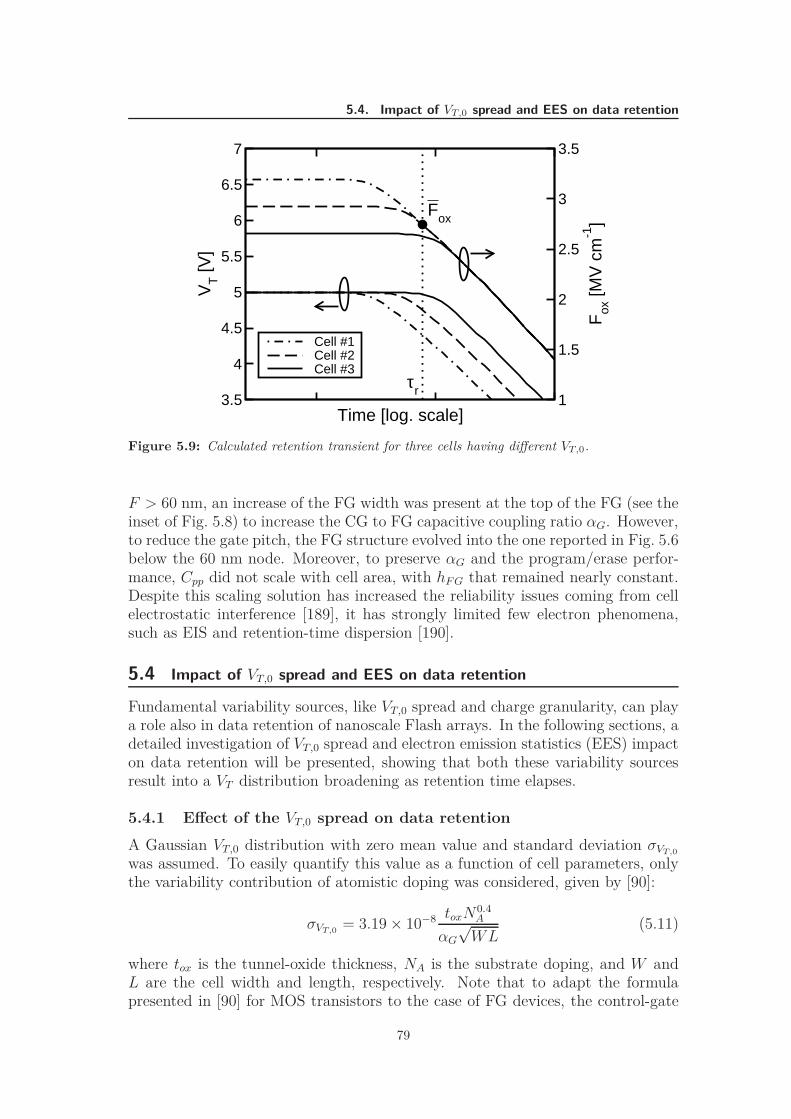
5.4. Impact of VT,0 spread and EES on data retention
Time [log. scale]3.5
4
4.5
5
5.5
6
6.5
7
VT [V
]
1
1.5
2
2.5
3
3.5
Fox
[MV
cm
-1]
Cell #1Cell #2Cell #3
Fox
τr
Figure 5.9: Calculated retention transient for three cells having different VT,0.
F > 60 nm, an increase of the FG width was present at the top of the FG (see theinset of Fig. 5.8) to increase the CG to FG capacitive coupling ratio αG. However,to reduce the gate pitch, the FG structure evolved into the one reported in Fig. 5.6below the 60 nm node. Moreover, to preserve αG and the program/erase perfor-mance, Cpp did not scale with cell area, with hF G that remained nearly constant.Despite this scaling solution has increased the reliability issues coming from cellelectrostatic interference [189], it has strongly limited few electron phenomena,such as EIS and retention-time dispersion [190].
5.4 Impact of VT,0 spread and EES on data retention
Fundamental variability sources, like VT,0 spread and charge granularity, can playa role also in data retention of nanoscale Flash arrays. In the following sections, adetailed investigation of VT,0 spread and electron emission statistics (EES) impacton data retention will be presented, showing that both these variability sourcesresult into a VT distribution broadening as retention time elapses.
5.4.1 Effect of the VT,0 spread on data retention
A Gaussian VT,0 distribution with zero mean value and standard deviation σVT,0
was assumed. To easily quantify this value as a function of cell parameters, onlythe variability contribution of atomistic doping was considered, given by [90]:
σVT,0= 3.19 × 10⁻⁸ toxN
0.4A
αG
√WL
(5.11)
where tox is the tunnel-oxide thickness, NA is the substrate doping, and W andL are the cell width and length, respectively. Note that to adapt the formulapresented in [90] for MOS transistors to the case of FG devices, the control-gate
79
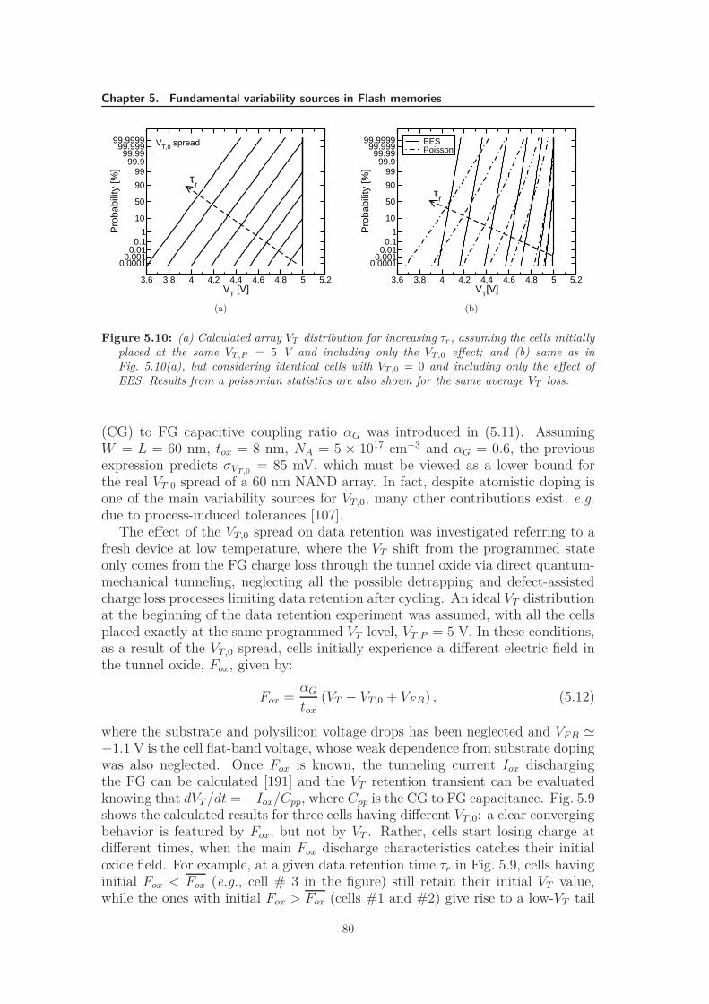
Chapter 5. Fundamental variability sources in Flash memories
3.6 3.8 4 4.2 4.4 4.6 4.8 5 5.2VT [V]
0.00010.001
0.010.1
1
10
50
90
9999.9
99.9999.999
99.9999
Pro
babi
lity
[%]
VT,0 spread
τr
(a)
3.6 3.8 4 4.2 4.4 4.6 4.8 5 5.2VT[V]
0.00010.001
0.010.1
1
10
50
90
9999.9
99.9999.999
99.9999
Pro
babi
lity
[%]
EESPoisson
τr
(b)
Figure 5.10: (a) Calculated array VT distribution for increasing τr, assuming the cells initiallyplaced at the same VT,P = 5 V and including only the VT,0 effect; and (b) same as inFig. 5.10(a), but considering identical cells with VT,0 = 0 and including only the effect ofEES. Results from a poissonian statistics are also shown for the same average VT loss.
(CG) to FG capacitive coupling ratio αG was introduced in (5.11). AssumingW = L = 60 nm, tox = 8 nm, NA = 5 × 1017 cm−3 and αG = 0.6, the previousexpression predicts σVT,0
= 85 mV, which must be viewed as a lower bound forthe real VT,0 spread of a 60 nm NAND array. In fact, despite atomistic doping isone of the main variability sources for VT,0, many other contributions exist, e.g.
due to process-induced tolerances [107].The effect of the VT,0 spread on data retention was investigated referring to a
fresh device at low temperature, where the VT shift from the programmed stateonly comes from the FG charge loss through the tunnel oxide via direct quantum-mechanical tunneling, neglecting all the possible detrapping and defect-assistedcharge loss processes limiting data retention after cycling. An ideal VT distributionat the beginning of the data retention experiment was assumed, with all the cellsplaced exactly at the same programmed VT level, VT,P = 5 V. In these conditions,as a result of the VT,0 spread, cells initially experience a different electric field inthe tunnel oxide, Fox, given by:
Fox =αG
tox(VT − VT,0 + VF B) , (5.12)
where the substrate and polysilicon voltage drops has been neglected and VF B ≃−1.1 V is the cell flat-band voltage, whose weak dependence from substrate dopingwas also neglected. Once Fox is known, the tunneling current Iox dischargingthe FG can be calculated [191] and the VT retention transient can be evaluatedknowing that dVT/dt = −Iox/Cpp, where Cpp is the CG to FG capacitance. Fig. 5.9shows the calculated results for three cells having different VT,0: a clear convergingbehavior is featured by Fox, but not by VT . Rather, cells start losing charge atdifferent times, when the main Fox discharge characteristics catches their initialoxide field. For example, at a given data retention time τr in Fig. 5.9, cells havinginitial Fox < Fox (e.g., cell # 3 in the figure) still retain their initial VT value,while the ones with initial Fox > Fox (cells #1 and #2) give rise to a low-VT tail
80
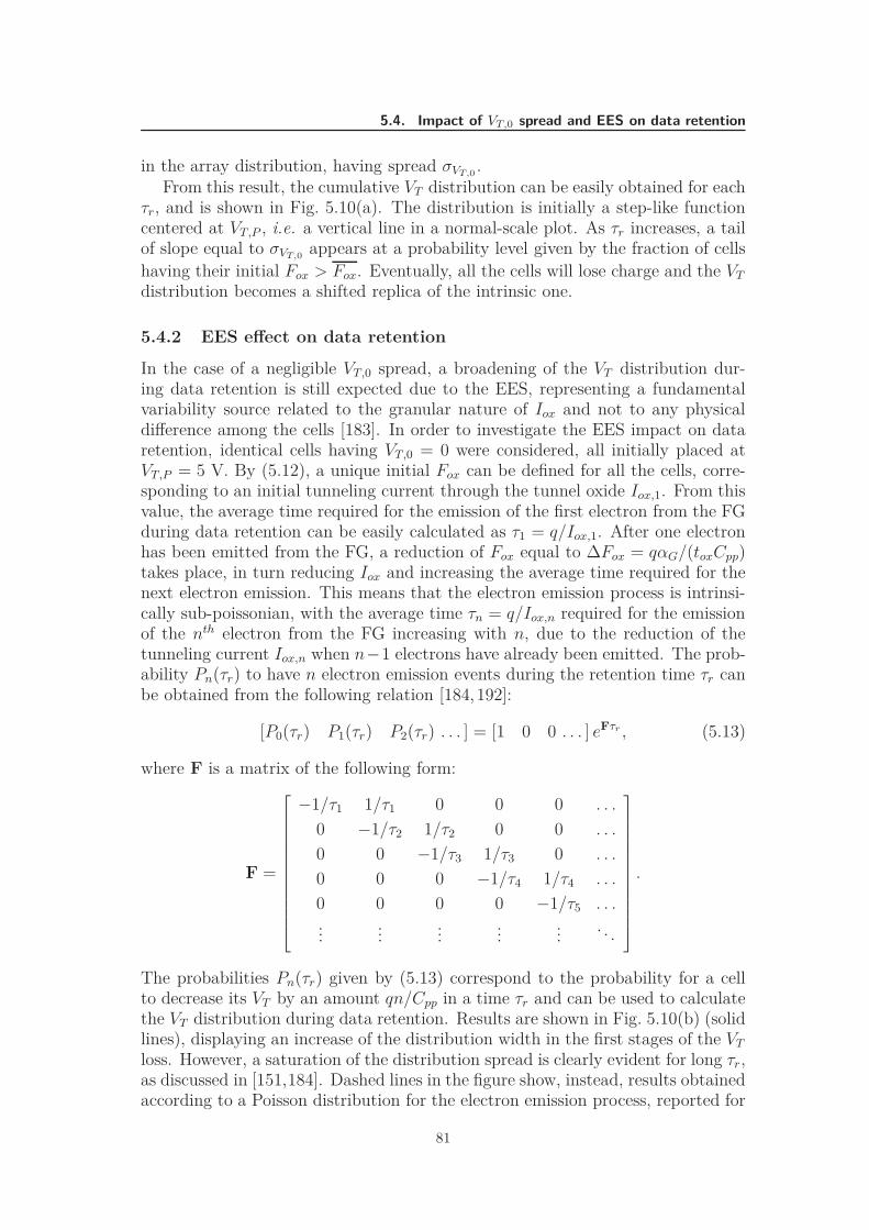
5.4. Impact of VT,0 spread and EES on data retention
in the array distribution, having spread σVT,0.
From this result, the cumulative VT distribution can be easily obtained for eachτr, and is shown in Fig. 5.10(a). The distribution is initially a step-like functioncentered at VT,P , i.e. a vertical line in a normal-scale plot. As τr increases, a tailof slope equal to σVT,0
appears at a probability level given by the fraction of cells
having their initial Fox > Fox. Eventually, all the cells will lose charge and the VT
distribution becomes a shifted replica of the intrinsic one.
5.4.2 EES effect on data retention
In the case of a negligible VT,0 spread, a broadening of the VT distribution dur-ing data retention is still expected due to the EES, representing a fundamentalvariability source related to the granular nature of Iox and not to any physicaldifference among the cells [183]. In order to investigate the EES impact on dataretention, identical cells having VT,0 = 0 were considered, all initially placed atVT,P = 5 V. By (5.12), a unique initial Fox can be defined for all the cells, corre-sponding to an initial tunneling current through the tunnel oxide Iox,1. From thisvalue, the average time required for the emission of the first electron from the FGduring data retention can be easily calculated as τ1 = q/Iox,1. After one electronhas been emitted from the FG, a reduction of Fox equal to ∆Fox = qαG/(toxCpp)takes place, in turn reducing Iox and increasing the average time required for thenext electron emission. This means that the electron emission process is intrinsi-cally sub-poissonian, with the average time τn = q/Iox,n required for the emissionof the nth electron from the FG increasing with n, due to the reduction of thetunneling current Iox,n when n−1 electrons have already been emitted. The prob-ability Pn(τr) to have n electron emission events during the retention time τr canbe obtained from the following relation [184,192]:
[P0(τr) P1(τr) P2(τr) . . . ] = [1 0 0 . . . ] eFτr , (5.13)
where F is a matrix of the following form:
F =
−1/τ1 1/τ1 0 0 0 . . .
0 −1/τ2 1/τ2 0 0 . . .
0 0 −1/τ3 1/τ3 0 . . .
0 0 0 −1/τ4 1/τ4 . . .
0 0 0 0 −1/τ5 . . ....
......
......
. . .
.
The probabilities Pn(τr) given by (5.13) correspond to the probability for a cellto decrease its VT by an amount qn/Cpp in a time τr and can be used to calculatethe VT distribution during data retention. Results are shown in Fig. 5.10(b) (solidlines), displaying an increase of the distribution width in the first stages of the VT
loss. However, a saturation of the distribution spread is clearly evident for long τr,as discussed in [151,184]. Dashed lines in the figure show, instead, results obtainedaccording to a Poisson distribution for the electron emission process, reported for
81
Chapter 5. Fundamental variability sources in Flash memories
0 0.2 0.4 0.6 0.8 1
∆VT [V]
0
0.2
0.4
0.6
0.8
1
1.2
1.4
1.6
∆VT [V
]
VT,0 spread
PoissonEES
0.2 0.4 0.6 0.8 1 1.20
0.2
0.4
0.6
0.8
1
1.2
1.4
1.6
∆VT [V
]
60nm tech. 32nm tech.
(a) (b)
Figure 5.11: Calculated edge VT loss as a function of the average loss for a 60 (a) and a 32 nm(b) NAND technology.
the same average VT loss. Clearly, such predictions largely over-estimate thedistribution spread when large VT losses are reached.
To compare the two effects previously discussed, Fig. 5.11a shows the calculatededge VT loss at a probability level equal to 10−5 (∆VT ) as a function of the averagearray VT loss (∆VT ), for the same τr. This representation is preferred to a plot ofthe rms value of the VT distribution at τr due to the asymmetrical shape of thedistributions of Fig. 5.10(a). Results are shown including either the VT,0 spread orthe EES contribution to data retention dispersion. It can be seen that the largeredge VT loss is given by the VT,0 spread, revealing that cell-to-cell parametervariations represent the dominant variability source for data retention (similarresults were also obtained starting from different VT,P distributions, having a non-zero width as a result of a non-ideal program operation). This is even more trueconsidering that only the atomistic doping contribution to σVT,0
has been heretaken into account and that the VT transients in Fig. 5.10(a) have been calculatedby (5.12) neglecting any statistical fluctuation in αG, tox and in the tunnelingcurrent Iox (due, for instance, to fluctuations in the curvature of the floating-gateedge). All these fluctuations represent additional cell-to-cell variability sourcesto be accounted for a comprehensive investigation of the statistical dispersion ofdata retention. Note also that if a poissonian approximation is (incorrectly) usedfor the EES (dashed line), its contribution to the spread of the VT distribution inFig. 5.10(b) continuously increases, eventually exceeding the intrinsic variability.Though this conclusion is wrong, it should be pointed out that the cross-overtakes place at quite large ∆VT , much larger than acceptable values for multi-levelNAND devices.
Finally, Fig. 5.11b shows that these same conclusions are valid for a 32 nm
82
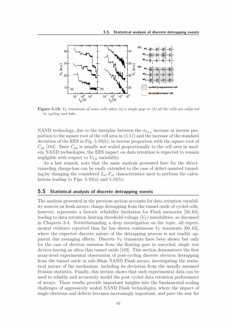
5.5. Statistical analysis of discrete detrapping events
Figure 5.12: VT transients of some cells when (a) a single page or (b) all the cells are subjectedto cycling and bake.
NAND technology, due to the interplay between the σVT,0increase in inverse pro-
portion to the square root of the cell area in (5.11) and the increase of the standarddeviation of the EES in Fig. 5.10(b), in inverse proportion with the square root ofCpp [184]. Since Cpp is usually not scaled proportionally to the cell area in mod-ern NAND technologies, the EES impact on data retention is expected to remainnegligible with respect to VT,0 variability.
As a last remark, note that the same analysis presented here for the direct-tunneling charge-loss can be easily extended to the case of defect-assisted tunnel-ing,by changing the considered Iox-Fox characteristics used to perform the calcu-lations leading to Figs. 5.10(a) and 5.10(b).
5.5 Statistical analysis of discrete detrapping events
The analysis presented in the previous section accounts for data retention variabil-ity sources on fresh arrays; charge detrapping from the tunnel oxide of cycled cells,however, represents a historic reliability limitation for Flash memories [58, 63],leading to data retention limiting threshold-voltage (VT ) instabilities, as discussedin Chapters 2-4. Notwithstanding a deep investigation on the topic, all experi-mental evidence reported thus far has shown continuous VT transients [60, 63],where the expected discrete nature of the detrapping process is not readily ap-parent due averaging effects. Discrete VT transients have been shown but onlyfor the case of electron emission from the floating gate in uncycled, single testdevices having an ultra-thin tunnel oxide [183]. This section demonstrate the firstarray-level experimental observation of post-cycling discrete electron detrappingfrom the tunnel oxide in sub-30nm NAND Flash arrays, investigating the statis-tical nature of the mechanism, including its deviation from the usually assumedPoisson statistics. Finally, this section shows that such experimental data can beused to reliably and accurately model the post cycled data retention performanceof arrays. These results provide important insights into the fundamental scalingchallenges of aggressively scaled NAND Flash technologies, where the impact ofsingle electrons and defects becomes increasingly important, and pave the way for
83
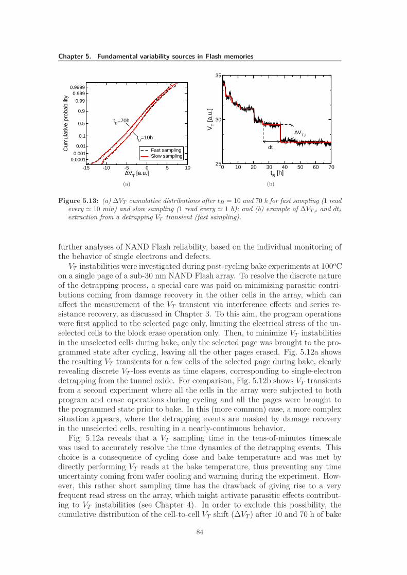
Chapter 5. Fundamental variability sources in Flash memories
-15 -10 -5 0 5 10∆VT [a.u.]
0.00010.001
0.01
0.1
0.5
0.9
0.99
0.9990.9999
Cum
ulat
ive
prob
abili
ty
Fast samplingSlow sampling
tB=10h
tB=70h
(a)
0 10 20 30 40 50 60 70tB [h]
25
30
35
VT [a
.u.]
dti
∆VT,i
(b)
Figure 5.13: (a) ∆VT cumulative distributions after tB = 10 and 70 h for fast sampling (1 readevery ≃ 10 min) and slow sampling (1 read every ≃ 1 h); and (b) example of ∆VT,i and dti
extraction from a detrapping VT transient (fast sampling).
further analyses of NAND Flash reliability, based on the individual monitoring ofthe behavior of single electrons and defects.VT instabilities were investigated during post-cycling bake experiments at 100oC
on a single page of a sub-30 nm NAND Flash array. To resolve the discrete natureof the detrapping process, a special care was paid on minimizing parasitic contri-butions coming from damage recovery in the other cells in the array, which canaffect the measurement of the VT transient via interference effects and series re-sistance recovery, as discussed in Chapter 3. To this aim, the program operationswere first applied to the selected page only, limiting the electrical stress of the un-selected cells to the block erase operation only. Then, to minimize VT instabilitiesin the unselected cells during bake, only the selected page was brought to the pro-grammed state after cycling, leaving all the other pages erased. Fig. 5.12a showsthe resulting VT transients for a few cells of the selected page during bake, clearlyrevealing discrete VT -loss events as time elapses, corresponding to single-electrondetrapping from the tunnel oxide. For comparison, Fig. 5.12b shows VT transientsfrom a second experiment where all the cells in the array were subjected to bothprogram and erase operations during cycling and all the pages were brought tothe programmed state prior to bake. In this (more common) case, a more complexsituation appears, where the detrapping events are masked by damage recoveryin the unselected cells, resulting in a nearly-continuous behavior.
Fig. 5.12a reveals that a VT sampling time in the tens-of-minutes timescalewas used to accurately resolve the time dynamics of the detrapping events. Thischoice is a consequence of cycling dose and bake temperature and was met bydirectly performing VT reads at the bake temperature, thus preventing any timeuncertainty coming from wafer cooling and warming during the experiment. How-ever, this rather short sampling time has the drawback of giving rise to a veryfrequent read stress on the array, which might activate parasitic effects contribut-ing to VT instabilities (see Chapter 4). In order to exclude this possibility, thecumulative distribution of the cell-to-cell VT shift (∆VT ) after 10 and 70 h of bake
84
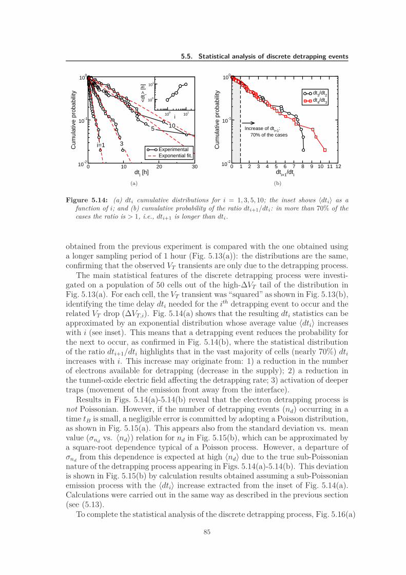
5.5. Statistical analysis of discrete detrapping events
0 10 20 30dti [h]
10-2
10-1
100
Cum
ulat
ive
prob
abili
ty
ExperimentalExponential fit.
100
101
i
100
101
<dt
i> [h
]i=1 3
5 10
(a)
0 1 2 3 4 5 6 7 8 9 10 11 12dti+1/dti
10-2
10-1
100
Cum
ulat
ive
prob
abili
ty dt3/dt2dt4/dt3
Increase of dti+1:70% of the cases
(b)
Figure 5.14: (a) dti cumulative distributions for i = 1, 3, 5, 10; the inset shows 〈dti〉 as afunction of i; and (b) cumulative probability of the ratio dti+1/dti: in more than 70% of thecases the ratio is > 1, i.e., dti+1 is longer than dti.
obtained from the previous experiment is compared with the one obtained usinga longer sampling period of 1 hour (Fig. 5.13(a)): the distributions are the same,confirming that the observed VT transients are only due to the detrapping process.
The main statistical features of the discrete detrapping process were investi-gated on a population of 50 cells out of the high-∆VT tail of the distribution inFig. 5.13(a). For each cell, the VT transient was “squared” as shown in Fig. 5.13(b),identifying the time delay dti needed for the ith detrapping event to occur and therelated VT drop (∆VT,i). Fig. 5.14(a) shows that the resulting dti statistics can beapproximated by an exponential distribution whose average value 〈dti〉 increaseswith i (see inset). This means that a detrapping event reduces the probability forthe next to occur, as confirmed in Fig. 5.14(b), where the statistical distributionof the ratio dti+1/dti highlights that in the vast majority of cells (nearly 70%) dtiincreases with i. This increase may originate from: 1) a reduction in the numberof electrons available for detrapping (decrease in the supply); 2) a reduction inthe tunnel-oxide electric field affecting the detrapping rate; 3) activation of deepertraps (movement of the emission front away from the interface).
Results in Figs. 5.14(a)-5.14(b) reveal that the electron detrapping process isnot Poissonian. However, if the number of detrapping events (nd) occurring in atime tB is small, a negligible error is committed by adopting a Poisson distribution,as shown in Fig. 5.15(a). This appears also from the standard deviation vs. meanvalue (σnd
vs. 〈nd〉) relation for nd in Fig. 5.15(b), which can be approximated bya square-root dependence typical of a Poisson process. However, a departure ofσnd
from this dependence is expected at high 〈nd〉 due to the true sub-Poissoniannature of the detrapping process appearing in Figs. 5.14(a)-5.14(b). This deviationis shown in Fig. 5.15(b) by calculation results obtained assuming a sub-Poissonianemission process with the 〈dti〉 increase extracted from the inset of Fig. 5.14(a).Calculations were carried out in the same way as described in the previous section(see (5.13).
To complete the statistical analysis of the discrete detrapping process, Fig. 5.16(a)
85
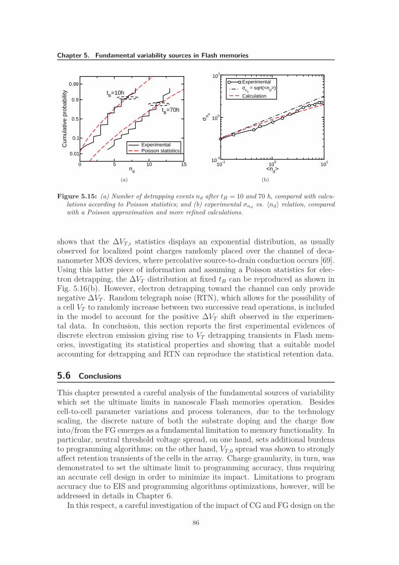
Chapter 5. Fundamental variability sources in Flash memories
0 5 10 15nd
0.01
0.1
0.5
0.9
0.99
Cum
ulat
ive
prob
abili
ty
ExperimentalPoisson statistics
tB=70h
tB=10h
(a)
10-1
100
101
<nd>
10-1
100
101
σ n d
Experimentalσnd
= sqrt(<nd>)
Calculation
(b)
Figure 5.15: (a) Number of detrapping events nd after tB = 10 and 70 h, compared with calcu-lations according to Poisson statistics; and (b) experimental σnd
vs. 〈nd〉 relation, comparedwith a Poisson approximation and more refined calculations.
shows that the ∆VT,i statistics displays an exponential distribution, as usuallyobserved for localized point charges randomly placed over the channel of deca-nanometer MOS devices, where percolative source-to-drain conduction occurs [69].Using this latter piece of information and assuming a Poisson statistics for elec-tron detrapping, the ∆VT distribution at fixed tB can be reproduced as shown inFig. 5.16(b). However, electron detrapping toward the channel can only providenegative ∆VT . Random telegraph noise (RTN), which allows for the possibility ofa cell VT to randomly increase between two successive read operations, is includedin the model to account for the positive ∆VT shift observed in the experimen-tal data. In conclusion, this section reports the first experimental evidences ofdiscrete electron emission giving rise to VT detrapping transients in Flash mem-ories, investigating its statistical properties and showing that a suitable modelaccounting for detrapping and RTN can reproduce the statistical retention data.
5.6 Conclusions
This chapter presented a careful analysis of the fundamental sources of variabilitywhich set the ultimate limits in nanoscale Flash memories operation. Besidescell-to-cell parameter variations and process tolerances, due to the technologyscaling, the discrete nature of both the substrate doping and the charge flowinto/from the FG emerges as a fundamental limitation to memory functionality. Inparticular, neutral threshold voltage spread, on one hand, sets additional burdensto programming algorithms; on the other hand, VT,0 spread was shown to stronglyaffect retention transients of the cells in the array. Charge granularity, in turn, wasdemonstrated to set the ultimate limit to programming accuracy, thus requiringan accurate cell design in order to minimize its impact. Limitations to programaccuracy due to EIS and programming algorithms optimizations, however, will beaddressed in details in Chapter 6.
In this respect, a careful investigation of the impact of CG and FG design on the
86
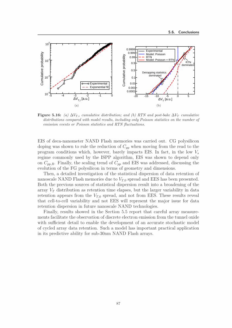
5.6. Conclusions
-5 -4 -3 -2 -1 0∆VT,i [a.u.]
10-3
10-2
10-1
100
Cum
ulat
ive
prob
abili
ty
ExperimentalExponential fit
(a)
-20 -15 -10 -5 0 5∆VT [a.u.]
0.00010.001
0.01
0.1
0.5
0.9
0.99
0.9990.9999
Cum
ulat
ive
prob
abili
ty
ExperimentalModel: PoissonRTNModel: Poisson + RTN
dominatedDetrapping statistics
dominatedRTN
(b)
Figure 5.16: (a) ∆VT,i cumulative distribution; and (b) RTN and post-bake ∆VT cumulativedistributions compared with model results, including only Poisson statistics on the number ofemission events or Poisson statistics and RTN fluctuations.
EIS of deca-nanometer NAND Flash memories was carried out. CG polysilicondoping was shown to rule the reduction of Cpp when moving from the read to theprogram conditions which, however, barely impacts EIS. In fact, in the low Vs
regime commonly used by the ISPP algorithm, EIS was shown to depend onlyon Cpp,R. Finally, the scaling trend of Cpp and EIS was addressed, discussing theevolution of the FG polysilicon in terms of geometry and dimensions.
Then, a detailed investigation of the statistical dispersion of data retention ofnanoscale NAND Flash memories due to VT,0 spread and EES has been presented.Both the previous sources of statistical dispersion result into a broadening of thearray VT distribution as retention time elapses, but the larger variability in dataretention appears from the VT,0 spread, and not from EES. These results revealthat cell-to-cell variability and not EES will represent the major issue for dataretention dispersion in future nanoscale NAND technologies.
Finally, results showed in the Section 5.5 report that careful array measure-ments facilitate the observation of discrete electron emission from the tunnel oxidewith sufficient detail to enable the development of an accurate stochastic modelof cycled array data retention. Such a model has important practical applicationin its predictive ability for sub-30nm NAND Flash arrays.
87

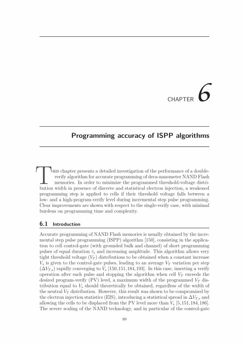
CHAPTER6
Programming accuracy of ISPP algorithms
This chapter presents a detailed investigation of the performance of a double-verify algorithm for accurate programming of deca-nanometer NAND Flashmemories. In order to minimize the programmed threshold-voltage distri-
bution width in presence of discrete and statistical electron injection, a weakenedprogramming step is applied to cells if their threshold voltage falls between alow- and a high-program-verify level during incremental step pulse programming.Clear improvements are shown with respect to the single-verify case, with minimalburdens on programming time and complexity.
6.1 Introduction
Accurate programming of NAND Flash memories is usually obtained by the incre-mental step pulse programming (ISPP) algorithm [150], consisting in the applica-tion to cell control-gate (with grounded bulk and channel) of short programmingpulses of equal duration τs and increasing amplitude. This algorithm allows verytight threshold voltage (VT ) distributions to be obtained when a constant increaseVs is given to the control-gate pulses, leading to an average VT variation per step(∆VT,s) rapidly converging to Vs [150,151,184,193]. In this case, inserting a verifyoperation after each pulse and stopping the algorithm when cell VT exceeds thedesired program-verify (PV) level, a maximum width of the programmed VT dis-tribution equal to Vs should theoretically be obtained, regardless of the width ofthe neutral VT distribution. However, this result was shown to be compromised bythe electron injection statistics (EIS), introducing a statistical spread in ∆VT,s andallowing the cells to be displaced from the PV level more than Vs [5,151,184,186].The severe scaling of the NAND technology, and in particular of the control-gate
89
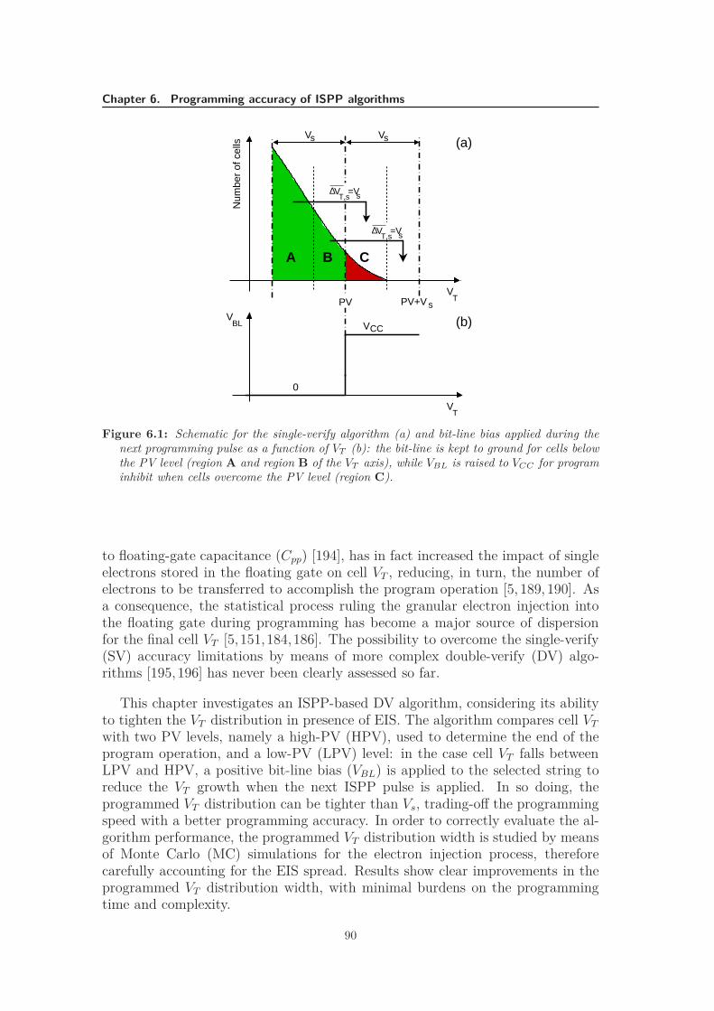
Chapter 6. Programming accuracy of ISPP algorithms
VTPV+V s
CCV
VT
VBL
Vs Vs
∆T,s
V =Vs
∆T,s
V =Vs
Num
ber
of c
ells
A B C
0
(a)
(b)
PV
Figure 6.1: Schematic for the single-verify algorithm (a) and bit-line bias applied during thenext programming pulse as a function of VT (b): the bit-line is kept to ground for cells belowthe PV level (region A and region B of the VT axis), while VBL is raised to VCC for programinhibit when cells overcome the PV level (region C).
to floating-gate capacitance (Cpp) [194], has in fact increased the impact of singleelectrons stored in the floating gate on cell VT , reducing, in turn, the number ofelectrons to be transferred to accomplish the program operation [5, 189, 190]. Asa consequence, the statistical process ruling the granular electron injection intothe floating gate during programming has become a major source of dispersionfor the final cell VT [5,151,184,186]. The possibility to overcome the single-verify(SV) accuracy limitations by means of more complex double-verify (DV) algo-rithms [195,196] has never been clearly assessed so far.
This chapter investigates an ISPP-based DV algorithm, considering its abilityto tighten the VT distribution in presence of EIS. The algorithm compares cell VT
with two PV levels, namely a high-PV (HPV), used to determine the end of theprogram operation, and a low-PV (LPV) level: in the case cell VT falls betweenLPV and HPV, a positive bit-line bias (VBL) is applied to the selected string toreduce the VT growth when the next ISPP pulse is applied. In so doing, theprogrammed VT distribution can be tighter than Vs, trading-off the programmingspeed with a better programming accuracy. In order to correctly evaluate the al-gorithm performance, the programmed VT distribution width is studied by meansof Monte Carlo (MC) simulations for the electron injection process, thereforecarefully accounting for the EIS spread. Results show clear improvements in theprogrammed VT distribution width, with minimal burdens on the programmingtime and complexity.
90
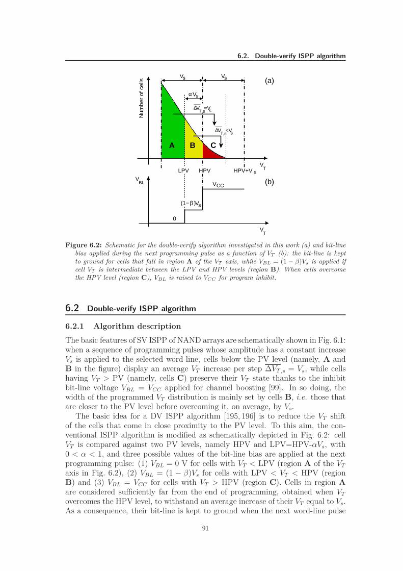
6.2. Double-verify ISPP algorithm
VT
CCV
VT
VBL
Vs Vs
HPV+V s
Vs(1− )β
Vsα
∆T,s
V =Vs
∆T,s
V <Vs
Num
ber
of c
ells
A B C
0
(a)
(b)
HPVLPV
Figure 6.2: Schematic for the double-verify algorithm investigated in this work (a) and bit-linebias applied during the next programming pulse as a function of VT (b): the bit-line is keptto ground for cells that fall in region A of the VT axis, while VBL = (1 − β)Vs is applied ifcell VT is intermediate between the LPV and HPV levels (region B). When cells overcomethe HPV level (region C), VBL is raised to VCC for program inhibit.
6.2 Double-verify ISPP algorithm
6.2.1 Algorithm description
The basic features of SV ISPP of NAND arrays are schematically shown in Fig. 6.1:when a sequence of programming pulses whose amplitude has a constant increaseVs is applied to the selected word-line, cells below the PV level (namely, A andB in the figure) display an average VT increase per step ∆VT ,s = Vs, while cellshaving VT > PV (namely, cells C) preserve their VT state thanks to the inhibitbit-line voltage VBL = VCC applied for channel boosting [99]. In so doing, thewidth of the programmed VT distribution is mainly set by cells B, i.e. those thatare closer to the PV level before overcoming it, on average, by Vs.
The basic idea for a DV ISPP algorithm [195, 196] is to reduce the VT shiftof the cells that come in close proximity to the PV level. To this aim, the con-ventional ISPP algorithm is modified as schematically depicted in Fig. 6.2: cellVT is compared against two PV levels, namely HPV and LPV=HPV-αVs, with0 < α < 1, and three possible values of the bit-line bias are applied at the nextprogramming pulse: (1) VBL = 0 V for cells with VT < LPV (region A of the VT
axis in Fig. 6.2), (2) VBL = (1 − β)Vs for cells with LPV < VT < HPV (regionB) and (3) VBL = VCC for cells with VT > HPV (region C). Cells in region Aare considered sufficiently far from the end of programming, obtained when VT
overcomes the HPV level, to withstand an average increase of their VT equal to Vs.As a consequence, their bit-line is kept to ground when the next word-line pulse
91
Chapter 6. Programming accuracy of ISPP algorithms
14 16 18 20 22 24 26Step #
0
1
2
3
4
VT [V
]
β=1β=0.5β=0
14 16 18 20 22 24 26Step #
15
16
17
18
19
20
VW
L [V]
Vs=500mV
(a)
14 16 18 20 22 24 26Step #
0.25
0.3
0.35
0.4
0.45
0.5
0.55
∆VT
,s [V
]
β=1β=0.5β=0 Vs=500mV
(b)
Figure 6.3: (a) Word-line bias applied during ISPP of the NAND cells (Vs = 500 mV). Theresulting average VT evolution from 103 MC simulations is also shown for the case β = 1(conventional ISPP algorithm), β = 0.5 and β = 0, starting applying the bit-line bias at step18; and (b) average ∆VT,s as a function of the programming step. At step 18 the bit-line bias
is applied, giving rise to a clear reduction of ∆VT ,s in the next steps with respect to Vs.
is applied as in the standard ISPP algorithm. Cells whose VT is above the LPVbut below the HPV level (region B) are instead close to the end of programming:a positive bit-line bias VBL = (1 −β)Vs (with β ≤ 1) is applied in this case duringall the following programming pulses. The bit-line bias applied to cells B aimsat reducing the increase of their tunnel-oxide electric field during the next pulsesand should, however, be sufficiently low to keep the string-select transistor ONduring program. In so doing, these cells will experience an average VT increasethat is lower than Vs, therefore limiting the maximum displacement they can havefrom the HPV level when they overcome it. Finally, cells having VT beyond theHPV level (region C) have reached the end of their programming transient andno further VT increase is needed. Therefore, their bit-line starts to be biased atVCC to inhibit the effect of the following word-line pulses.
6.2.2 Effect of a bit-line bias on the ISPP transients
Figs. 6.3(a)-6.3(b) display the average behavior out of 103 MC simulations forthe VT transient during ISPP, in the case of β = 1, 0.5 and 0. The MC model,originally presented and validated against experimental data in [151] for SV ISPP,reproduces the discrete electron injection during programming, correctly describ-ing the tunnel-oxide field variations due to (1) electron storage in the FG, (2)word-line bias increase and, in the case of the DV algorithm, (3) bit-line biasincrease (more details on the simulation procedure will be given in the next Sec-tion). The same neutral VT was initially assumed for the cells. Fig. 6.3(a) showsthe staircase waveform applied to the selected word-line (Vs = 500 mV) and thesimulated average VT evolution in the case β = 1 (circles), clearly displaying∆VT ,s = Vs. Note, in fact, that β = 1 represents the reference programming tran-sient, with no bit-line bias applied, and should be compared to the β = 0.5 andβ = 0 cases, corresponding to VBL = 250 mV and 500 mV. The bit-line bias was
92
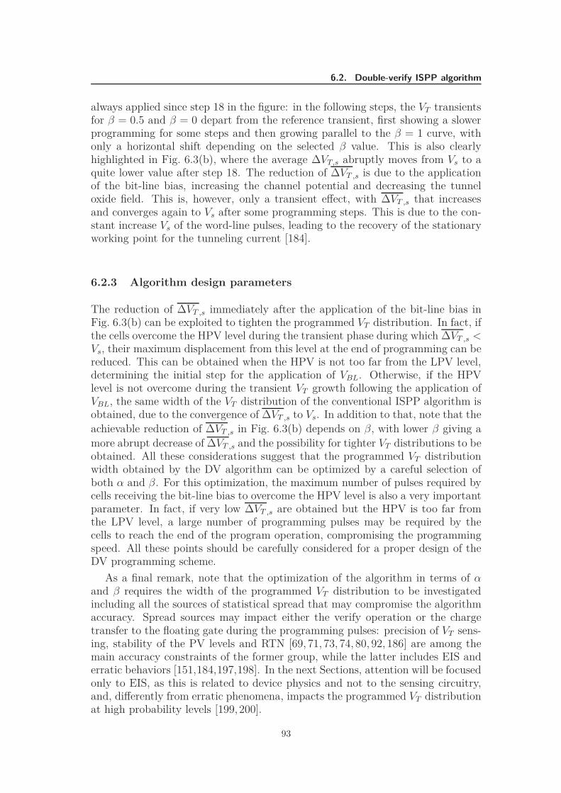
6.2. Double-verify ISPP algorithm
always applied since step 18 in the figure: in the following steps, the VT transientsfor β = 0.5 and β = 0 depart from the reference transient, first showing a slowerprogramming for some steps and then growing parallel to the β = 1 curve, withonly a horizontal shift depending on the selected β value. This is also clearlyhighlighted in Fig. 6.3(b), where the average ∆VT,s abruptly moves from Vs to aquite lower value after step 18. The reduction of ∆VT ,s is due to the applicationof the bit-line bias, increasing the channel potential and decreasing the tunneloxide field. This is, however, only a transient effect, with ∆VT ,s that increasesand converges again to Vs after some programming steps. This is due to the con-stant increase Vs of the word-line pulses, leading to the recovery of the stationaryworking point for the tunneling current [184].
6.2.3 Algorithm design parameters
The reduction of ∆VT ,s immediately after the application of the bit-line bias inFig. 6.3(b) can be exploited to tighten the programmed VT distribution. In fact, ifthe cells overcome the HPV level during the transient phase during which ∆VT ,s <Vs, their maximum displacement from this level at the end of programming can bereduced. This can be obtained when the HPV is not too far from the LPV level,determining the initial step for the application of VBL. Otherwise, if the HPVlevel is not overcome during the transient VT growth following the application ofVBL, the same width of the VT distribution of the conventional ISPP algorithm isobtained, due to the convergence of ∆VT ,s to Vs. In addition to that, note that the
achievable reduction of ∆VT ,s in Fig. 6.3(b) depends on β, with lower β giving a
more abrupt decrease of ∆VT ,s and the possibility for tighter VT distributions to beobtained. All these considerations suggest that the programmed VT distributionwidth obtained by the DV algorithm can be optimized by a careful selection ofboth α and β. For this optimization, the maximum number of pulses required bycells receiving the bit-line bias to overcome the HPV level is also a very importantparameter. In fact, if very low ∆VT ,s are obtained but the HPV is too far fromthe LPV level, a large number of programming pulses may be required by thecells to reach the end of the program operation, compromising the programmingspeed. All these points should be carefully considered for a proper design of theDV programming scheme.
As a final remark, note that the optimization of the algorithm in terms of αand β requires the width of the programmed VT distribution to be investigatedincluding all the sources of statistical spread that may compromise the algorithmaccuracy. Spread sources may impact either the verify operation or the chargetransfer to the floating gate during the programming pulses: precision of VT sens-ing, stability of the PV levels and RTN [69, 71, 73, 74, 80, 92, 186] are among themain accuracy constraints of the former group, while the latter includes EIS anderratic behaviors [151,184,197,198]. In the next Sections, attention will be focusedonly to EIS, as this is related to device physics and not to the sensing circuitry,and, differently from erratic phenomena, impacts the programmed VT distributionat high probability levels [199, 200].
93
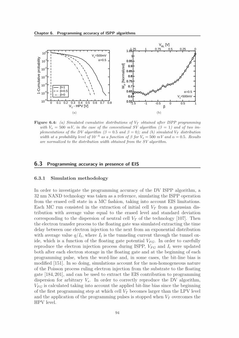
Chapter 6. Programming accuracy of ISPP algorithms
0 0.1 0.2 0.3 0.4 0.5 0.6 0.7 0.8VT - HPV [V]
10-6
10-5
10-4
10-3
10-2
10-1
100
1-C
umul
ativ
e pr
obab
ility
β=1β=0.5β=0
Vs=500mV
α=0.5
(a)
-1.5 -1 -0.5 0 0.5 1β
0.55
0.6
0.65
0.7
0.75
0.8
0.85
0.9
0.95
1
1.05
WP [N
orm
aliz
ed]
1.25 1 0.75 0.5 0.25 0VBL [V]
0.55
0.6
0.65
0.7
0.75
0.8
0.85
0.9
0.95
1
1.05
α=0.5
Vs=500mV
(b)
Figure 6.4: (a) Simulated cumulative distributions of VT obtained after ISPP programmingwith Vs = 500 mV, in the case of the conventional SV algorithm (β = 1) and of two im-plementations of the DV algorithm (β = 0.5 and β = 0); and (b) simulated VT distributionwidth at a probability level of 10−4 as a function of β for Vs = 500 mV and α = 0.5. Resultsare normalized to the distribution width obtained from the SV algorithm.
6.3 Programming accuracy in presence of EIS
6.3.1 Simulation methodology
In order to investigate the programming accuracy of the DV ISPP algorithm, a32 nm NAND technology was taken as a reference, simulating the ISPP operationfrom the erased cell state in a MC fashion, taking into account EIS limitations.Each MC run consisted in the extraction of initial cell VT from a gaussian dis-tribution with average value equal to the erased level and standard deviationcorresponding to the dispersion of neutral cell VT of the technology [107]. Thenthe electron transfer process to the floating gate was simulated extracting the timedelay between one electron injection to the next from an exponential distributionwith average value q/It, where It is the tunneling current through the tunnel ox-ide, which is a function of the floating gate potential VF G. In order to carefullyreproduce the electron injection process during ISPP, VF G and It were updatedboth after each electron storage in the floating gate and at the beginning of eachprogramming pulse, when the word-line and, in some cases, the bit-line bias ismodified [151]. In so doing, simulations account for the non-homogeneous natureof the Poisson process ruling electron injection from the substrate to the floatinggate [184, 201], and can be used to extract the EIS contribution to programmingdispersion for arbitrary Vs. In order to correctly reproduce the DV algorithm,VF G is calculated taking into account the applied bit-line bias since the beginningof the first programming step at which cell VT becomes larger than the LPV leveland the application of the programming pulses is stopped when VT overcomes theHPV level.
94
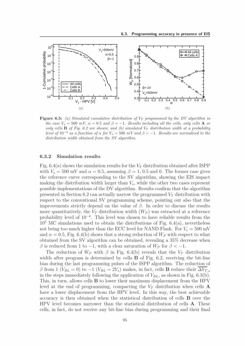
6.3. Programming accuracy in presence of EIS
0 0.1 0.2 0.3 0.4 0.5VT - HPV [V]
10-6
10-5
10-4
10-3
10-2
10-1
100
1-C
umul
ativ
e pr
obab
ility
All cellsCells ACells B
Vs=500mV
α=0.5β=-1
(a)
0 0.1 0.2 0.3 0.4 0.5 0.6 0.7 0.8 0.9α
0.3
0.4
0.5
0.6
0.7
0.8
0.9
1
WP [N
orm
aliz
ed]
All cellsCells A
Vs=500mV
β=-1V
(b)
Figure 6.5: (a) Simulated cumulative distribution of VT programmed by the DV algorithm inthe case Vs = 500 mV, α = 0.5 and β = −1. Results including all the cells, only cells A oronly cells B of Fig. 6.2 are shown; and (b) simulated VT distribution width at a probabilitylevel of 10−4 as a function of α for Vs = 500 mV and β = −1. Results are normalized to thedistribution width obtained from the SV algorithm.
6.3.2 Simulation results
Fig. 6.4(a) shows the simulation results for the VT distribution obtained after ISPPwith Vs = 500 mV and α = 0.5, assuming β = 1, 0.5 and 0. The former case givesthe reference curve corresponding to the SV algorithm, showing the EIS impactmaking the distribution width larger than Vs, while the other two cases representpossible implementations of the DV algorithm. Results confirm that the algorithmpresented in Section 6.2 can actually narrow the programmed VT distribution withrespect to the conventional SV programming scheme, pointing out also that theimprovements strictly depend on the value of β. In order to discuss the resultsmore quantitatively, the VT distribution width (WP ) was extracted at a referenceprobability level of 10−4. This level was chosen to have reliable results from the105 MC simulations used to obtain the distributions of Fig. 6.4(a), neverthelessnot being too much higher than the ECC level for NAND Flash. For Vs = 500 mVand α = 0.5, Fig. 6.4(b) shows that a strong reduction of WP with respect to whatobtained from the SV algorithm can be obtained, revealing a 35% decrease whenβ is reduced from 1 to −1, with a clear saturation of WP for β < −1.
The reduction of WP with β in Fig. 6.4(b) reveals that the VT distributionwidth after program is determined by cells B of Fig. 6.2, receiving the bit-linebias during the last programming pulses of the ISPP algorithm. The reduction ofβ from 1 (VBL = 0) to −1 (VBL = 2Vs) makes, in fact, cells B reduce their ∆VT ,s
in the steps immediately following the application of VBL, as shown in Fig. 6.3(b).This, in turn, allows cells B to lower their maximum displacement from the HPVlevel at the end of programming, compacting the VT distribution when cells Ahave a lower displacement from the HPV level. In this way, the best achievableaccuracy is then obtained when the statistical distribution of cells B over theHPV level becomes narrower than the statistical distribution of cells A. Thesecells, in fact, do not receive any bit-line bias during programming and their final
95
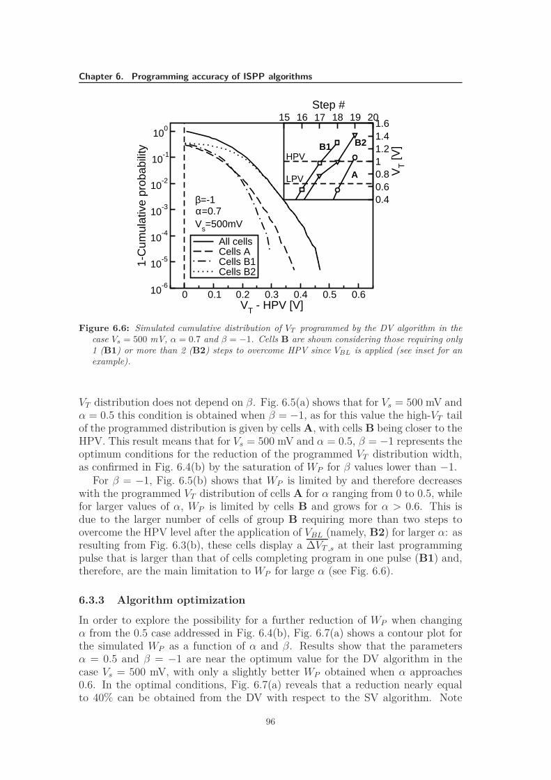
Chapter 6. Programming accuracy of ISPP algorithms
0 0.1 0.2 0.3 0.4 0.5 0.6VT - HPV [V]
10-6
10-5
10-4
10-3
10-2
10-1
100
1-C
umul
ativ
e pr
obab
ility
All cellsCells ACells B1Cells B2
15 16 17 18 19 20Step #
0.40.60.811.21.41.6
VT [V
]
Vs=500mVα=0.7β=-1
HPV
LPV
B1 B2
A
Figure 6.6: Simulated cumulative distribution of VT programmed by the DV algorithm in thecase Vs = 500 mV, α = 0.7 and β = −1. Cells B are shown considering those requiring only1 (B1) or more than 2 (B2) steps to overcome HPV since VBL is applied (see inset for anexample).
VT distribution does not depend on β. Fig. 6.5(a) shows that for Vs = 500 mV andα = 0.5 this condition is obtained when β = −1, as for this value the high-VT tailof the programmed distribution is given by cells A, with cells B being closer to theHPV. This result means that for Vs = 500 mV and α = 0.5, β = −1 represents theoptimum conditions for the reduction of the programmed VT distribution width,as confirmed in Fig. 6.4(b) by the saturation of WP for β values lower than −1.
For β = −1, Fig. 6.5(b) shows that WP is limited by and therefore decreaseswith the programmed VT distribution of cells A for α ranging from 0 to 0.5, whilefor larger values of α, WP is limited by cells B and grows for α > 0.6. This isdue to the larger number of cells of group B requiring more than two steps toovercome the HPV level after the application of VBL (namely, B2) for larger α: asresulting from Fig. 6.3(b), these cells display a ∆VT ,s at their last programmingpulse that is larger than that of cells completing program in one pulse (B1) and,therefore, are the main limitation to WP for large α (see Fig. 6.6).
6.3.3 Algorithm optimization
In order to explore the possibility for a further reduction of WP when changingα from the 0.5 case addressed in Fig. 6.4(b), Fig. 6.7(a) shows a contour plot forthe simulated WP as a function of α and β. Results show that the parametersα = 0.5 and β = −1 are near the optimum value for the DV algorithm in thecase Vs = 500 mV, with only a slightly better WP obtained when α approaches0.6. In the optimal conditions, Fig. 6.7(a) reveals that a reduction nearly equalto 40% can be obtained from the DV with respect to the SV algorithm. Note
96
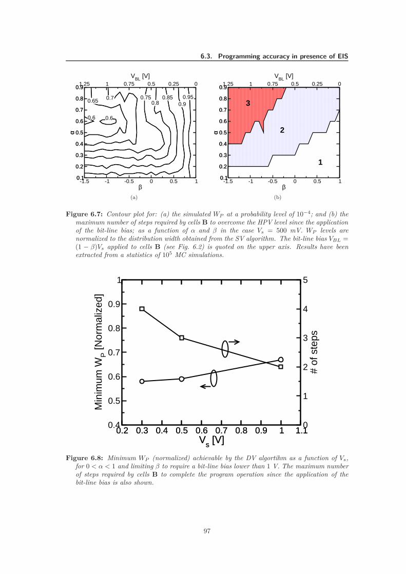
6.3. Programming accuracy in presence of EIS
-1.5 -1 -0.5 0 0.5 1β
0.1
0.2
0.3
0.4
0.5
0.6
0.7
0.8
0.9
α
1.25 1 0.75 0.5 0.25 0VBL [V]
0.1
0.2
0.3
0.4
0.5
0.6
0.7
0.8
0.9
α
0.950.9
0.850.8
0.750.70.65
0.6 0.6
(a)
-1.5 -1 -0.5 0 0.5 1β
0.1
0.2
0.3
0.4
0.5
0.6
0.7
0.8
0.9
α
1.25 1 0.75 0.5 0.25 0VBL [V]
0.1
0.2
0.3
0.4
0.5
0.6
0.7
0.8
0.9
α 2
3
1
(b)
Figure 6.7: Contour plot for: (a) the simulated WP at a probability level of 10−4; and (b) themaximum number of steps required by cells B to overcome the HPV level since the applicationof the bit-line bias; as a function of α and β in the case Vs = 500 mV. WP levels arenormalized to the distribution width obtained from the SV algorithm. The bit-line bias VBL =(1 − β)Vs applied to cells B (see Fig. 6.2) is quoted on the upper axis. Results have beenextracted from a statistics of 105 MC simulations.
0.2 0.3 0.4 0.5 0.6 0.7 0.8 0.9 1 1.1Vs [V]
0.4
0.5
0.6
0.7
0.8
0.9
1
Min
imum
WP [N
orm
aliz
ed]
0.2 0.3 0.4 0.5 0.6 0.7 0.8 0.9 1 1.1Vs [V]
0
1
2
3
4
5
# of
ste
ps
Figure 6.8: Minimum WP (normalized) achievable by the DV algortihm as a function of Vs,for 0 < α < 1 and limiting β to require a bit-line bias lower than 1 V. The maximum numberof steps required by cells B to complete the program operation since the application of thebit-line bias is also shown.
97
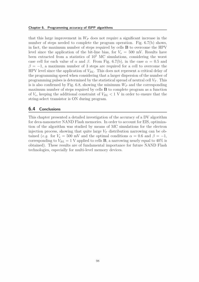
Chapter 6. Programming accuracy of ISPP algorithms
that this large improvement in WP does not require a significant increase in thenumber of steps needed to complete the program operation. Fig. 6.7(b) shows,in fact, the maximum number of steps required by cells B to overcome the HPVlevel since the application of the bit-line bias, for Vs = 500 mV. Results havebeen extracted from a statistics of 105 MC simulations, considering the worstcase cell for each value of α and β. From Fig. 6.7(b), in the case α = 0.5 andβ = −1, a maximum number of 3 steps are required for a cell to overcome theHPV level since the application of VBL. This does not represent a critical delay ofthe programming speed when considering that a larger dispersion of the number ofprogramming pulses is determined by the statistical spread of neutral cell VT . Thisis is also confirmed by Fig. 6.8, showing the minimum WP and the correspondingmaximum number of steps required by cells B to complete program as a functionof Vs, keeping the additional constraint of VBL < 1 V in order to ensure that thestring-select transistor is ON during program.
6.4 Conclusions
This chapter presented a detailed investigation of the accuracy of a DV algorithmfor deca-nanometer NAND Flash memories. In order to account for EIS, optimiza-tion of the algorithm was studied by means of MC simulations for the electroninjection process, showing that quite large VT distribution narrowing can be ob-tained (e.g. for Vs = 500 mV and the optimal conditions α = 0.6 and β = −1,corresponding to VBL = 1 V applied to cells B, a narrowing nearly equal to 40% isobtained). These results are of fundamental importance for future NAND Flashtechnologies, especially for multi-level memory devices.
98
Summary of results
The research activity carried out during the Ph.D. program was focused onthe reliability constraints of decananometer Flash memories and resultedin a deep understanding from a physical standpoint of the emerging fail-
ure mechanisms which affect Flash operation and set the ultimate limits to thetechnology scaling. Experimental activities and modeling efforts, including MonteCarlo modeling of programming algorithms, analytical modeling of electron injec-tion/emission statistics, analysis of post-cycling threshold voltage instabilities andcompact modeling of NAND string current, aimed at the characterization of a widerange of physical mechanisms, such as few electron phenomena, variability sourcesof cell parameters, tunnel oxide and IPD degradation due to electron trapping/de-trapping and interface state creation/annealing, electrostatic interference betweenadjacent cells, impact of short channel effects and mobility degradation on NANDstring current. The careful analysis of these mechanisms and the assessment oftheir impact on Flash reliability allowed to determine the fundamental scalinglimitations and to propose feasible solutions for the future technology nodes, con-sisting in cell and algorithm design and optimization. Experimental and modelingactivities, moreover, were devoted to the design of characterization techniques forultra-scaled Flash technologies: accelerated testing schemes for the evaluation ofdistributed cycling effects and threshold voltage instabilities during data reten-tion, in fact, emerged as a challenging and demanding task for Flash qualificationand the impact of this research activity was recognized by both the semiconductorindustry and the scientific community, since the main results achieved in this fieldwere cited by JEDEC documents and awarded at the 2012 IEEE InternationalPhysics Reliability Symposium (see the List of Publications for more details).
In order to assess the constraints to post-cycling data retention, the atten-tion was focused to cycling-induced damage creation and post-cycling thresholdvoltage instabilities, which were investigated under a wide range of experimen-tal conditions. This analysis led to the assessment and validation of a univer-sal damage-recovery model, allowing the development of accelerated qualificationschemes which accurately reproduce the real on-field usage of the memory device.
99
Summary of results
Spurious effects which may emerge during the testing procedure itself, compromis-ing the activation energy evaluation and the correct interpretation of distributed-cycling qualification schemes were also addressed, gaining a deep understandingof qualification schemes for nanoscale Flash devices. From a physical standpoint,damage creation and recovery dynamics and mechanisms were addressed via com-pact modeling of NAND string current. This approach allowed to evaluate theimpact of electrostatics interference and short channel effect on NAND operationand to identify the major failure oxide degradation and recovery mechanisms, con-sisting in the charge trapping / detrapping in the oxide and in the interface statecreation / annealing. The analysis of threshold voltage instabilities revealed thatthe latter mechanism comes into play when cell threshold voltage is monitored athigh read current, due to carrier mobility degradation. Results show that thresh-old voltage instabilities are increased and their activation energy is lowered withrespect to the usual 1.1 eV value given by charge detrapping whenever the satu-ration value of the string current moves too close to read current, thus, providinguseful hints for the design of the read scheme and the choice of the operatingvoltages of the memory array.
Then, the investigation of few electron phenomena highlighted that cell stateis controlled by a low number of electrons, which progressively decreases with sizescaling, and, thus, the granularity of the charge flux into the floating gate emergedas a source of program noise, setting the ultimate limit to programming accuracy.In this regards, a careful investigation of the impact of CG and FG design on theelectron injection statistics (EIS) of decananometer NAND Flash memories wascarried out, discussing the EIS scaling trend and the evolution of the FG designin terms of geometry and dimensions. Moreover, a detailed investigation of theaccuracy of programming algorithms was performed by means of Monte Carlosimulations for the electron injection process, showing that narrower programmeddistribution can be obtained with an optimized double-verify ISPP algorithm,with respect to a standard single-verify ISPP scheme, with minimal burdens onalgorithm complexity and programming speed. These results are of fundamentalimportance for future NAND Flash technologies, especially for multi-level mem-ory devices. Then, the impact of few electron phenomena also on data retentionwas taken into account, investigating the statistical dispersion of data retentionof nanoscale NAND Flash memories due to neutral threshold voltage spread andelectron emission statistics (EES): both the phenomena results in a distributionwidening during retention, but the modeling results reveal that cell-to-cell vari-ability and not EES will represent the major issue for data retention dispersion offresh devices in future nanoscale technologies. Finally, single electron detrappingfrom tunnel oxide during post-cycling retention was experimentally demonstratedin the sub-30 nm regime and a statistical model was developed, showing that post-cycling data retention variability is ruled by detrapping statistics in aggressivelyscaled Flash technologies.
In conclusion, this research activity provided the physical understanding, themodeling tools and the characterization techniques required to investigate the reli-ability of the state-of-the-art Flash memory technologies; the most of the emergingmechanisms, moreover, will likely affect also the future generations of charge-based
100
memory technologies, including planar and 3D Flash architectures, and, thus, thisthesis provides the reference against novel memories should be tested, in order toassess the improvements with respect to the conventional Flash technology.
101

Bibliography
[1] R. Micheloni, L. Crippa, and A. Marelli, Inside NAND Flash Memories. Springer, 2010.
[2] A. Maconi, Performance and Limitations of Charge-Trap Storage for Non-Volatile Memory Tech-nologies. PhD thesis, Politecnico di Milano - Doctoral Program in Information Technology, 2011.
[3] F. Masuoka, M. Momodomi, Y. Iwata, and R. Shirota, “New ultra high density EPROM andFlash EEPROM with NAND structure cell,” in IEDM Tech. Dig., pp. 552–555, 1987.
[4] K. Kim, “Future memory technology: challenges and opportunities,” in VLSI-TSA Tech. Dig.,pp. 5–9, 2008.
[5] K. Prall and K. Parat, “25 nm 64 Gb MLC NAND technology and scaling challenges,” in IEDMTech. Dig., pp. 102–105, 2010.
[6] S. Lai, “Non-volatile memory technology: the quest for ever lower cost,” in IEDM Tech. Dig.,pp. 1–6, 2008.
[7] C. M. Compagnoni, A. S. Spinelli, A. L. Lacaita, A. Ghetti, and A. Visconti, NONVOLATILEMEMORIES -Materials, Devices and Applications, ch. Emerging Constraints on NAND FlashMemory Reliability. American Scientific Publishers, 2012.
[8] D. Kahng and S. Sze, “A floating-gate and its application to memory devices,” in The Bell SystemTechnical Journal, pp. 1288–1295, 1967.
[9] S. Aritome, S. Satoh, T. Maruyama, H. Watanabe, S. Shuto, G. Hemink, R. Shirota, S. Watanabe,and F. Masuoka, “A 0.67µm2 self-aligned shallow trench isolation cell (SA-STI cell) for 3 V-only256 Mbit NAND EEPROMs,” in IEDM Tech. Dig., pp. 61–64, 1994.
[10] “International technology roadmap for semiconductors,” 2009.
[11] T. Kamigaichi, F. Arai, H. Nitsuta, M. Endo, K. Nishihara, T. Murata, H. Takekida, T. Izumi,K. Uchida, T. Maruyama, I. Kawabata, Y. Suyama, A. Sato, K. Ueno, H. Takeshita, Y. Joko,S. Watanabe, Y. Liu, H. Meguro, A. Kajita, Y. Ozawa, and T. Watanabe, “Floating gate supermulti level NAND Flash memory technology for 30 nm and beyond,” in IEDM Tech. Dig., pp. 827–830, 2008.
[12] H. Nitta, T. Kamigaichi, F. Arai, T. Futatsuyama, M. Endo, N. Nishihara, T. Murata,H. Takekida, T. Izumi, K. Uchida, T. Maruyama, I. Kawabata, Y. Suyama, A. Sato, K. Ueno,H. Takeshita, Y. Joko, S. Watanabe, Y. Liu, H. Meguro, A. Kajita, Y. Ozawa, Y. Takeuchi,T. Hara, and T. Watanabe, “Three bits per cell floating gate NAND Flash memory technologyfor 30 nm and beyond,” in Proc. IRPS, pp. 307–310, 2009.
[13] M. Park, K. Kim, J.-H. Park, and J.-H. Choi, “Direct field effect of neighboring cell transistor oncell-to-cell interference of NAND Flash cell arrays,” IEEE Electron Device Lett., vol. 30, pp. 174–177, Feb. 2009.
[14] G. Servalli, D. Brazzelli, E. Camerlenghi, G. Capetti, S. Costantini, C. Cupeta, D. DeSimone,A. Ghetti, T. Ghilardi, P. Gulli, M. Mariani, A. Pavan, and R. Somaschini, “A 65 nm NOR Flashtechnology with 0.042 µm2 cell size for high performance multilevel application,” in IEDM Tech.Dig., pp. 869–872, 2005.
103
Bibliography
[15] D. James, “Nano-Scale Flash in the Mid-Decade,” in ASMC 2007. IEEE/SEMI, pp. 371–376,2007.
[16] K. Takeuchi, Y. Kameda, S. Fujimura, H. Otake, K. Hosono, H. Shiga, Y. Watanabe, T. Futat-suyama, Y. Shindo, M. Kojima, M. Iwai, M. Shirakawa, M. Ichige, K. Hatakeyama, S. Tanaka,T. Kamei, J.-Y. Fu, A. Cernea, Y. Li, M. Higashitani, G. Hemink, S. Sato, K. Oowada, S.-C. Lee,N. Hayashida, J. Wan, J. Lutze, S. Tsao, M. Mofidi, K. Sakurai, N. Tokiwa, H. Waki, Y. Nozawa,K. Kanazawa, and S. Ohshima, “A 56-nm CMOS 99-mm2 8-Gb multi-level NAND Flash memorywith 10-MB/s program throughput,” IEEE J. Solid-State Circuits, vol. 42, pp. 219–232, Jan.2007.
[17] D. Nobunaga, E. Abedifard, F. Roohparvar, J. Lee, E. Yu, A. Vahidimowlavi, M. Abraham,S. Talreja, E. Sundaram, R. Rozman, L. Vu, C. L. Chen, U. Chandrasekhar, R. Bains, V. Viajedor,W. Mak, M. Choi, D. Udeshi, M. Luo, S. Qureshi, J. Tsai, F. Jaffin, Y. Liu, and M. Mancinelli,“A 50 nm 8 Gb NAND Flash memory with 100 MB/s program throughput and 200 MB/s DDRinterface,” in Proc. ISSCC, pp. 426–427, 2008.
[18] C. Trinh, N. Shibata, T. Nakano, M. Ogawa, J. Sato, Y. Takeyama, K. Isobe, B. Le, F. Moogat,N. Mokhlesi, K. Kozazai, P. Hong, T. Kamei, K. Iwasa, J. Nakai, T. Shimizu, M. Honma, S. Sakai,T. Kawaai, S. Hoshi, J. Yuh, C. Hsu, T. Tseng, J. Li, J. Hu, M. Liu, S. Khalid, J. Chen, M. Watan-abe, H. Lin, J. Yang, K. McKay, K. Nguyen, T. Pham, Y. Matsuda, K. Nakamura, K. Kanebako,S. Yoshikawa, W. Igarashi, A. Inoue, T. Takahashi, Y. Komatsu, C. Suzuki, K. Kanazawa, M. Hi-gashitani, S. Lee, T. Murai, K. Nguyen, J. Lan, S. Huynh, M. Murin, M. Shlick, M. Lasser,R. Cernea, M. Mofidi, K. Schuegraf, and K. Quader, “A 5.6 MB/s 64 Gb 4 b/cell NAND Flashmemory in 43 nm CMOS,” in Proc. ISSCC, pp. 246–247, 2009.
[19] P. Pavan, R. Bez, P. Olivo, and E. Zanoni, “Flash memory cells - an overview,” Proc. IEEE,vol. 85, pp. 1248–1271, Aug. 1997.
[20] K.-T. Park, O. Kwon, S. Yoon, M.-H. Choi, I.-M. Kim, B.-G. Kim, M.-S. Kim, Y.-H. Choi, S.-H.Shin, Y. Song, J.-Y. Park, J.-E. Lee, C.-G. Eun, H.-C. Lee, H.-J. Kim, J.-H. Lee, J.-Y. Kim,T.-M. Kweon, H.-J. Yoon, T. Kim, D.-K. Shim, J. Sel, J.-Y. Shin, P. Kwak, J.-M. Han, K.-S.Kim, S. Lee, Y.-H. Lim, and T.-S. Jung, “A 7MB/s 64Gb 3-bit/cell DDR NAND Flash memoryin 20nm-node technology,” in ISSCC Tech. Dig., pp. 212–213, 2011.
[21] M. Goldman, K. Pangal, G. Naso, and A. Goda, “25nm 64Gb 130mm2 3bpc NAND Flash Mem-ory,” in Proc. IMW, pp. 1–4, 2011.
[22] J. Hwang, J. Seo, Y. Lee, S. Park, J. Leem, J. Kim, T. Hong, S. Jeong, K. Lee, H. Heo, H. Lee,P. Jang, K. Park, M. Lee, S. Baik, J. Kim, H. Kkang, M. Jang, J. Lee, G. Cho, J. Lee, B. Lee,H. Jang, S. Park, J. Kim, S. Lee, S. Aritome, S. Hong, and S. Park, “A middle-1x nm NANDFlash memory cell (M1X-NAND) with highly manufacturable integration technologies,” in IEDMTech. Dig., pp. 199–202, 2011.
[23] D. J. DiMaria and E. Cartier, “Mechanism for stress-induced leakage currents in thin silicondioxide films,” J. Appl. Phys., vol. 78, pp. 3883–3894, 1995.
[24] P. Samanta, “Hole trapping due to anode hole injection in thin tunnel gate oxides in memorydevices under Fowler-Nordheim stress,” Applied Physics Letters, vol. 75, pp. 2966–2968, Nov.1999.
[25] D. Ielmini, A. S. Spinelli, A. L. Lacaita, and M. J. van Duuren, “Defect generation statistics inthin gate oxides,” IEEE Trans. Electron Devices, vol. 51, pp. 1288–1295, Aug. 2004.
[26] D. Ielmini, A. S. Spinelli, A. L. Lacaita, and A. Modelli, “A new two-trap tunneling model forthe anomalous SILC in flash memories,” Microelectron. Eng., vol. 59, pp. 189–195, 2001.
[27] J. Maserjian and N. Zamani, “Observation of positively charged state generation near the Si/SiO2
interface during Fowler-Nordheim tunneling,” J. Vac. Sci. Technol., vol. 20, pp. 743–746, 1982.
[28] D. A. Baglee and M. C. Smayling, “The effects of write/erase cycling on data loss in EEPROMs,”in IEDM Tech. Dig., pp. 624–626, 1985.
[29] P. Olivo, T. N. Nguyen, and B. Riccò, “High-field-induced degradation in ultra-thin SiO2 films,”IEEE Trans. Electron Devices, vol. 35, pp. 2259–2267, Dec. 1988.
[30] K. Naruke, S. Taguchi, and M. Wada, “Stress induced leakage current limiting to scale downEEPROM tunnel oxide thickness,” in IEDM Tech. Dig., pp. 424–427, 1988.
104
Bibliography
[31] R. Rofan and C. Hu, “Stress-induced oxide leakage,” IEEE Electron Device Lett., vol. 12, pp. 632–634, Nov. 1991.
[32] R. Moazzami and C. Hu, “Stress-induced current in thin silicon dioxide films,” in IEDM Tech.Dig., pp. 139–142, 1992.
[33] S. Aritome, R. Shirota, G. Hemink, T. Endoh, and F. Masuoka, “Reliability issues of Flashmemory cells,” Proc. IEEE, vol. 81, pp. 776–788, May 1993.
[34] P. P. Apte and K. C. Saraswat, “Correlation of trap generation to charge-to-breakdown (Qbd):A physical-damage model for of dielectric breakdown,” IEEE Trans. Electron Devices, vol. 41,pp. 1595–1602, Sept. 1994.
[35] H. Satake and A. Toriumi, “Common origin for stress-induced leakage current and electron trapgeneration in SiO2,” Appl. Phys. Lett., vol. 67, pp. 3489–3490, 1995.
[36] S. Yamada, K. Amemiya, T. Yamane, H. Hazama, and K. Hashimoto, “Non-uniform current flowthrough thin oxide after Fowler-Nordheim current stress,” in Proc. IRPS, pp. 108–112, 1996.
[37] M. Kimura and T. Ohmi, “Conduction mechanism and origin of stress-induced leakage current inthin silicon dioxide films,” J. Appl. Phys., vol. 80, pp. 6360–6369, 1996.
[38] N. Matsukawa, S. Yamada, K. Amemiya, and H. Hazama, “A hot hole-induced low-level leakagecurrent in thin silicon dioxide films,” IEEE Trans. Electron Devices, vol. 43, pp. 1924–1929, Nov.1996.
[39] G. J. Hemink, K. Shimizu, S. Aritome, and R. Shirota, “Trapped hole enhanced stress inducedleakage current in NAND EEPROM tunnel oxides,” in Proc. IRPS, pp. 117–121, 1996.
[40] J. D. Blauwe, J. Van Houdt, D. Wellekens, R. Degraeve, P. Roussel, L. Haseslagh, L. Defern,G. Groeseneken, and H. E. Maes, “A new quantitative model to predict SILC-related disturbcharacteristics in Flash E2PROM devices,” in IEDM Tech. Dig., pp. 343–346, 1996.
[41] E. F. Runnion, S. M. Gladstone, R. S. Scott, D. J. Dumin, L. Lie, and J. C. Mitros, “Thicknessdependence of stress-induced leakage currents in silicon oxide,” IEEE Trans. Electron Devices,vol. 44, pp. 993–1001, 1997.
[42] K. Sakakibara, N. Ajika, M. Hatanaka, H. Miyoshi, and A. Yasuoka, “Identification of stress-induced leakage current components and the corresponding trap models in SiO2 films,” IEEETrans. Electron Devices, vol. 44, pp. 2267–2273, June 1997.
[43] K. Sakakibara, N. Ajika, K. Eikyu, K. Ishikawa, and H. Miyoshi, “A quantitative analysis of time-decay reproducible stress-induced leakage current in SiO2 films,” IEEE Trans. Electron Devices,vol. 44, pp. 1002–1007, June 1997.
[44] S. Satoh, G. Hemink, K. Hatakeyama, and S. Aritome, “Stress-induced leakage current of tunneloxide derived from Flash memory read-disturb characteristics,” IEEE Trans. Electron Devices,vol. 45, pp. 482–486, Feb. 1998.
[45] J. D. Blauwe, J. Van Houdt, D. Wellekens, G. Groeseneken, and H. E. Maes, “SILC-related effectsin Flash E2PROM’s–Part I: A quantitative model for steady-state SILC,” IEEE Trans. ElectronDevices, vol. 45, pp. 1745–1750, Aug. 1998.
[46] J. D. Blauwe, J. Van Houdt, D. Wellekens, G. Groeseneken, and H. E. Maes, “SILC-related effectsin Flash E2PROM’s–Part II: Prediction of steady-state SILC-related disturb characteristics,”IEEE Trans. Electron Devices, vol. 45, pp. 1751–1760, Aug. 1998.
[47] G. B. Alers, B. E. Weir, M. A. Alam, G. L. Timp, and T. Sorch, “Trap assisted tunneling as amechanism of degradation and noise,” in Proc. IRPS, pp. 76–79, 1998.
[48] S. Takagi, M. Takayanagi, and A. Toriumi, “Experimental examination of physical model for directtunneling current in unstressed/stressed ultrathin gate oxides,” in IEDM Tech. Dig., pp. 461–464,1999.
[49] D. Ielmini, A. S. Spinelli, M. A. Rigamonti, and A. L. Lacaita, “Modeling of SILC based onelectron and hole tunneling – Part I: Transient effects,” IEEE Trans. Electron Devices, vol. 47,pp. 1258–1265, June 2000.
[50] D. Ielmini, A. S. Spinelli, M. A. Rigamonti, and A. L. Lacaita, “Modeling of SILC based on electronand hole tunneling – Part II: Steady-state,” IEEE Trans. Electron Devices, vol. 47, pp. 1266–1272,June 2000.
105
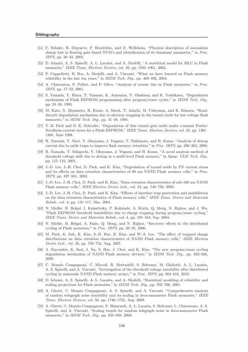
Bibliography
[51] F. Schuler, R. Degraeve, P. Hendrickx, and D. Wellekens, “Physical description of anomalouscharge loss in floating gate based NVM’s and identification of its dominant parameter,” in Proc.IRPS, pp. 26–33, 2002.
[52] D. Ielmini, A. S. Spinelli, A. L. Lacaita, and A. Modelli, “A statistical model for SILC in Flashmemories,” IEEE Trans. Electron Devices, vol. 49, pp. 1955–1961, 2002.
[53] P. Cappelletti, R. Bez, A. Modelli, and A. Visconti, “What we have learned on Flash memoryreliability in the last ten years,” in IEDM Tech. Dig., pp. 489–492, 2004.
[54] A. Chimenton, P. Pellati, and P. Olivo, “Analysis of erratic bits in Flash memories,” in Proc.IRPS, pp. 17–22, 2001.
[55] S. Yamada, Y. Hiura, T. Yamane, K. Amemiya, Y. Ohshima, and K. Yoshikawa, “Degradationmechanism of Flash EEPROM programming after program/erase cycles,” in IEDM Tech. Dig.,pp. 23–26, 1993.
[56] M. Kato, N. Miyamoto, H. Kume, A. Satoh, T. Adachi, M. Ushiyama, and K. Kimura, “Read-disturb degradation mechanism due to electron trapping in the tunnel oxide for low-voltage flashmemories,” in IEDM Tech. Dig., pp. 45–48, 1994.
[57] Y.-B. Park and D. K. Schroder, “Degradation of thin tunnel gate oxide under constant Fowler-Nordheim current stress for a Flash EEPROM,” IEEE Trans. Electron Devices, vol. 45, pp. 1361–1368, June 1998.
[58] R. Yamada, Y. Mori, Y. Okuyama, J. Yugami, T. Nishimoto, and H. Kume, “Analysis of detrapcurrent due to oxide traps to improve flash memory retention,” in Proc. IRPS, pp. 200–204, 2000.
[59] R. Yamada, T. Sekiguchi, Y. Okuyama, J. Yugami, and H. Kume, “A novel analysis method ofthreshold voltage shift due to detrap in a multi-level Flash memory,” in Symp. VLSI Tech. Dig.,pp. 115–116, 2001.
[60] J.-D. Lee, J.-H. Choi, D. Park, and K. Kim, “Degradation of tunnel oxide by FN current stressand its effects on data retention characteristics of 90 nm NAND Flash memory cells,” in Proc.IRPS, pp. 497–501, 2003.
[61] J.-D. Lee, J.-H. Choi, D. Park, and K. Kim, “Data retention characteristics of sub-100 nm NANDFlash memory cells,” IEEE Electron Device Lett., vol. 24, pp. 748–750, 2003.
[62] J.-D. Lee, J.-H. Choi, D. Park, and K. Kim, “Effects of interface trap generation and annihilationon the data retention characteristics of Flash memory cells,” IEEE Trans. Device and MaterialsReliab., vol. 4, pp. 110–117, Mar. 2004.
[63] N. Mielke, H. Belgal, I. Kalastirsky, P. Kalavade, A. Kurtz, Q. Meng, N. Righos, and J. Wu,“Flash EEPROM threshold instabilities due to charge trapping during program/erase cycling,”IEEE Trans. Device and Materials Reliab., vol. 4, pp. 335–344, Sep. 2004.
[64] N. Mielke, H. Belgal, A. Fazio, Q. Meng, and N. Righos, “Recovery effects in the distributedcycling of Flash memories,” in Proc. IRPS, pp. 29–35, 2006.
[65] M. Park, K. Suh, K. Kim, S.-H. Hur, K. Kim, and W.-S. Lee, “The effect of trapped chargedistributions on data retention characteristics of NAND Flash memory cells,” IEEE ElectronDevice Lett., vol. 28, pp. 750–752, Aug. 2007.
[66] A. Fayrushin, K. Seol, J. Na, S. Hur, J. Choi, and K. Kim, “The new program/erase cyclingdegradation mechanism of NAND Flash memory devices,” in IEDM Tech. Dig., pp. 823–826,2009.
[67] C. Monzio Compagnoni, C. Miccoli, R. Mottadelli, S. Beltrami, M. Ghidotti, A. L. Lacaita,A. S. Spinelli, and A. Visconti, “Investigation of the threshold voltage instability after distributedcycling in nanoscale NAND Flash memory arrays,” in Proc. IRPS, pp. 604–610, 2010.
[68] D. Ielmini, A. S. Spinelli, A. L. Lacaita, and A. Modelli, “Statistical modeling of reliability andscaling projections for Flash memories,” in IEDM Tech. Dig., pp. 703–706, 2001.
[69] A. Ghetti, C. Monzio Compagnoni, A. S. Spinelli, and A. Visconti, “Comprehensive analysisof random telegraph noise instability and its scaling in deca-nanometer Flash memories,” IEEETrans. Electron Devices, vol. 56, pp. 1746–1752, Aug. 2009.
[70] A. Ghetti, C. Monzio Compagnoni, F. Biancardi, A. L. Lacaita, S. Beltrami, L. Chiavarone, A. S.Spinelli, and A. Visconti, “Scaling trends for random telegraph noise in deca-nanometer Flashmemories,” in IEDM Tech. Dig., pp. 835–838, 2008.
106
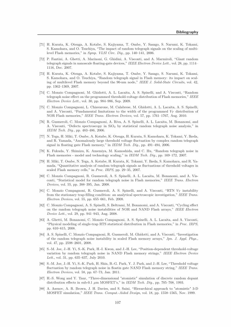
Bibliography
[71] H. Kurata, K. Otsuga, A. Kotabe, S. Kajiyama, T. Osabe, Y. Sasago, S. Narumi, K. Tokami,S. Kamohara, and O. Tsuchiya, “The impact of random telegraph signals on the scaling of multi-level Flash memories,” in Symp. VLSI Circ. Dig., pp. 140–141, 2006.
[72] P. Fantini, A. Ghetti, A. Marinoni, G. Ghidini, A. Visconti, and A. Marmiroli, “Giant randomtelegraph signals in nanoscale floating-gate devices,” IEEE Electron Device Lett., vol. 28, pp. 1114–1116, Dec. 2007.
[73] H. Kurata, K. Otsuga, A. Kotabe, S. Kajiyama, T. Osabe, Y. Sasago, S. Narumi, K. Tokami,S. Kamohara, and O. Tsuchiya, “Random telegraph signal in Flash memory: its impact on scal-ing of multilevel Flash memory beyond the 90-nm node,” IEEE J. Solid-State Circuits, vol. 42,pp. 1362–1369, 2007.
[74] C. Monzio Compagnoni, M. Ghidotti, A. L. Lacaita, A. S. Spinelli, and A. Visconti, “Randomtelegraph noise effect on the programmed threshold-voltage distribution of Flash memories,” IEEEElectron Device Lett., vol. 30, pp. 984–986, Sep. 2009.
[75] C. Monzio Compagnoni, L. Chiavarone, M. Calabrese, M. Ghidotti, A. L. Lacaita, A. S. Spinelli,and A. Visconti, “Fundamental limitations to the width of the programmed VT distribution ofNOR Flash memories,” IEEE Trans. Electron Devices, vol. 57, pp. 1761–1767, Aug. 2010.
[76] R. Gusmeroli, C. Monzio Compagnoni, A. Riva, A. S. Spinelli, A. L. Lacaita, M. Bonanomi, andA. Visconti, “Defects spectroscopy in SiO2 by statistical random telegraph noise analysis,” inIEDM Tech. Dig., pp. 483–486, 2006.
[77] N. Tega, H. Miki, T. Osabe, A. Kotabe, K. Otsuga, H. Kurata, S. Kamohara, K. Tokami, Y. Ikeda,and R. Yamada, “Anomalously large threshold voltage fluctuation by complex random telegraphsignal in floating gate Flash memory,” in IEDM Tech. Dig., pp. 491–494, 2006.
[78] K. Fukuda, Y. Shimizu, K. Amemiya, M. Kamoshida, and C. Hu, “Random telegraph noise inFlash memories - model and technology scaling,” in IEDM Tech. Dig., pp. 169–172, 2007.
[79] H. Miki, T. Osabe, N. Tega, A. Kotabe, H. Kurata, K. Tokami, Y. Ikeda, S. Kamohara, and R. Ya-mada, “Quantitative analysis of random telegraph signals as fluctuations of threshold voltages inscaled Flash memory cells,” in Proc. IRPS, pp. 29–35, 2007.
[80] C. Monzio Compagnoni, R. Gusmeroli, A. S. Spinelli, A. L. Lacaita, M. Bonanomi, and A. Vis-conti, “Statistical model for random telegraph noise in Flash memories,” IEEE Trans. ElectronDevices, vol. 55, pp. 388–395, Jan. 2008.
[81] C. Monzio Compagnoni, R. Gusmeroli, A. S. Spinelli, and A. Visconti, “RTN VT instabilityfrom the stationary trap-filling condition: an analytical spectroscopic investigation,” IEEE Trans.Electron Devices, vol. 55, pp. 655–661, Feb. 2008.
[82] C. Monzio Compagnoni, A. S. Spinelli, S. Beltrami, M. Bonanomi, and A. Visconti, “Cycling effecton the random telegraph noise instabilities of NOR and NAND Flash arrays,” IEEE ElectronDevice Lett., vol. 29, pp. 941–943, Aug. 2008.
[83] A. Ghetti, M. Bonanomi, C. Monzio Compagnoni, A. S. Spinelli, A. L. Lacaita, and A. Visconti,“Physical modeling of single-trap RTS statistical distribution in Flash memories,” in Proc. IRPS,pp. 610–615, 2008.
[84] A. S. Spinelli, C. Monzio Compagnoni, R. Gusmeroli, M. Ghidotti, and A. Visconti, “Investigationof the random telegraph noise instability in scaled Flash memory arrays,” Jpn. J. Appl. Phys.,vol. 47, pp. 2598–2601, 2008.
[85] S.-M. Joe, J.-H. Yi, S.-K. Park, H.-I. Kwon, and J.-H. Lee, “Position-dependent threshold-voltagevariation by random telegraph noise in NAND Flash memory strings,” IEEE Electron DeviceLett., vol. 31, pp. 635–637, July 2010.
[86] S.-M. Joe, J.-H. Yi, S.-K. Park, H. Shin, B.-G. Park, Y. J. Park, and J.-H. Lee, “Threshold voltagefluctuation by random telegraph noise in floatin gate NAND Flash memory string,” IEEE Trans.Electron Devices, vol. 58, pp. 67–73, Jan. 2011.
[87] H.-S. Wong and Y. Taur, “Three-dimensional "atomistic" simulation of discrete random dopantdistribution effects in sub-0.1 µm MOSFET’s,” in IEDM Tech. Dig., pp. 705–708, 1993.
[88] A. Asenov, A. R. Brown, J. H. Davies, and S. Saini, “Hierarchical approach to "atomistic" 3-DMOSFET simulation,” IEEE Trans. Comput.-Aided Design, vol. 18, pp. 1558–1565, Nov. 1999.
107
Bibliography
[89] N. Sano, K. Matsuzawa, M. Mukai, and N. Nakayama, “On discrete random dopant modellingin drift-diffusion simulations: physical meaning of "atomistic" dopants,” Microelectron. Reliab.,vol. 42, pp. 189–199, 2002.
[90] A. Asenov, A. R. Brown, J. H. Davies, S. Kaya, and G. Slavcheva, “Simulation of intrinsicparameter fluctuations in decananometer and nanometer-scale MOSFETs,” IEEE Trans. ElectronDevices, vol. 50, pp. 1837–1852, Sep. 2003.
[91] G. Roy, A. R. Brown, F. Adamu-Lema, S. Roy, and A. Asenov, “Simulation study of individualand combined sources of intrinsic parameter fluctuations in conventional Nano-MOSFETs,” IEEETrans. Electron Devices, vol. 52, pp. 3063–3070, May 2006.
[92] K. Sonoda, K. Ishikawa, T. Eimori, and O. Tsuchiya, “Discrete dopant effects on statisticalvariation of random telegraph signal magnitude,” IEEE Trans. Electron Devices, vol. 54, pp. 1918–1925, Aug. 2007.
[93] M. F. Bukhori, S. Roy, and A. Asenov, “Statistical aspects of reliability in bulk MOSFETs withmultiple defect states and random discrete dopants,” Microelectron. Reliab., vol. 48, pp. 1549–1552, Sep. 2008.
[94] H. H. Mueller and M. Schulz, “Random telegraph signal: An atomic probe of the local current infield-effect transistors,” J. Appl. Phys., vol. 83, pp. 1734–1741, 1998.
[95] A. Asenov, R. Balasubramaniam, A. R. Brown, J. H. Davies, and S. Saini, “Random telegraphsignal amplitudes in sub 100 nm (decanano) MOSFETs: a 3d "atomistic" simulation study,” inIEDM Tech. Dig., pp. 279–282, 2000.
[96] A. Asenov, R. Balasubramaniam, A. R. Brown, and J. H. Davies, “RTS amplitudes in decana-nometer MOSFETs: 3-D simulation study,” IEEE Trans. Electron Devices, vol. 50, pp. 839–845,Mar. 2003.
[97] J.-D. Lee, C.-K. Lee, M.-W. Lee, H.-S. Kim, K.-C. Park, and W.-S. Lee, “A new programmingdisturbance phenomenon in NAND Flash memory by source/drain hot-electrons generated byGIDL current,” in Proc. Non-Volatile Semiconductor Memory Workshop, pp. 31–33, 2006.
[98] M. Kang, W. Hahn, I. H. Park, J. Park, Y. Song, H. Lee, C. Eun, S. Ju, K. Choi, Y. Lim, S. Jang,S. Cho, B.-G. Park, and H. Shin, “DIBL-Induced program disturb characteristics in 32-nm NANDFlash memory array,” IEEE Trans. Electron Devices, vol. 58, pp. 3626–3629, Oct. 2011.
[99] K.-D. Suh, B.-H. Suh, Y.-H. Lim, J.-K. Kim, Y.-J. Choi, Y.-N. Koh, S.-S. Lee, S.-C. Kwon, B.-S.Choi, J.-S. Yum, J.-H. Choi, J.-R. Kim, and H.-K. Lim, “A 3.3 V 32 Mb NAND Flash memorywith incremental step pulse programming scheme,” IEEE J. Solid-State Circuits, vol. 30, no. 11,pp. 1149–1156, 1995.
[100] S. Satoh, H. Hagiwara, T. Tanzawa, K. Takeuchi, and R. Shirota, “A novel isolation-scalingtechnology for NAND EEPROMs with the minimized program disturbance,” in IEDM Tech.Dig., pp. 291–294, 1997.
[101] J.-D. Choi, S.-S. Cho, Y.-S. Yim, J.-D. Lee, H.-S. Kim, K.-J. Joo, S.-H. Hur, H.-S. Im, J. kim,J.-W. Lee, K.-I.Seo, M.-S. Kang, K.-H. Kim, J.-L. Nam, K.-C. Park, and M.-Y. Lee, “Highlymanufacturable 1Gb NAND Flash using 0.12 µm process technology,” in IEDM Tech. Dig., pp. 25–28, 2001.
[102] S. Seo, H. Kim, S. Park, S. Lee, S. Aritome, and S. Hong, “Novel negative VT shift programdisturb phenomena in 2x ∼ 3x nm nand flash memory cells,” in Proc. IRPS, pp. 6B.2.1–6B.2.4,2011.
[103] B. Cho, C. Lee, K. Seol, S. Hur, J. Choi, J. Choi, and C. Chung, “A new cell-to-cell interferenceinduced by conduction band distortion near S/D region in scaled NAND Flash memories,” inProc. IMW, pp. 1–4, 2011.
[104] E. Kwon, D. Oh, B. Lee, J. hyong Yi, S. Kim, G. Cho, S. Park, and J. Choi, “An abnormal floatinggate interference and a low program performance in 2y nm NAND Flash devices,” in SISPADConf. Proc., pp. 207–210, 2011.
[105] K.-T. Park, M. Kang, D. Kim, S.-W. Hwang, B. Y. Choi, Y.-T. Lee, C. Kim, and K. Kim,“A zeroing cell-to-cell interference page architecture with temporary LSB storing and parallelMSB program scheme for MLC NAND Flash memories,” IEEE J. Solid-State Circuits, vol. 43,pp. 919–928, Apr. 2008.
108
Bibliography
[106] C.-H. Lee, S.-K. Sung, D. Jang, S. Lee, S. Choi, J. Kim, S. Park, M. Song, H.-C. Baek, E. Ahn,J. Shin, K. Shin, K. Min, S.-S. Cho, C.-J. Kang, J. Choi, K. Kim, J.-H. Choi, K.-D. Suh, andT.-S. Jung, “A highly manufacturable integration technology for 27 nm 2 and 3 bit/cell NANDFlash memory,” in IEDM Tech. Dig., pp. 98–101, 2010.
[107] A. Spessot, A. Calderoni, P. Fantini, A. S. Spinelli, C. Monzio Compagnoni, F. Farina, A. L.Lacaita, and A. Marmiroli, “Variability effects on the VT distribution of nanoscale NAND Flashmemories,” in Proc. IRPS, pp. 970–974, 2010.
[108] A. Ghetti, L. Bortesi, and L. Vendrame, “3D simulation study of gate coupling and gate cross-interference in advanced floating gate non-volatile memories,” Solid-State Electron., vol. 49,pp. 1805–1812, 2005.
[109] C. Lee, S.-K. Lee, S. Ahn, J. Lee, W. Park, Y. Cho, C. Jang, C. Yang, S. Chung, I.-S. Yun, B. Joo,B. Jeong, J. Kim, J. Kwon, H. Jin, Y. Noh, J. Ha, M. Sung, D. Choi, S. Kim, J. Choi, T. Jeon,H. Park, J.-S. Yang, and Y.-H. Koh, “A 32-Gb MLC NAND Flash memory with Vth enduranceenhancing schemes in 32 nm CMOS,” Solid-State Circuits, IEEE Journal of, vol. 46, pp. 97–106,Jan. 2011.
[110] P. Blomme, M. Rosmeulen, A. Cacciato, M. Kostermans, C. Vrancke, S. V. Aerde, T. Schram,I. Debusschere, M. Jurczak, and J. V. Houdt, “Novel dual layer floating gate structure as enablerof fully planar flash memory,” in Symp. VLSI TechnologyTech. Dig, pp. 129–130, 2010.
[111] D. Wellekens, P. Blomme, M. Rosmeulen, T. Schram, A. Cacciato, I. Debusschere, J. Van Houdt,and S. Van Aerde, “An ultra-thin hybrid floating gate concept for Sub-20nm NAND Flash tech-nologies,” in Proc. IMW, pp. 1–4, 2011.
[112] J. V. Houdt, “Charge-based nonvolatile memory: Near the end of the roadmap?,” Current AppliedPhysics, vol. 11, no. 2, Supplement, pp. e21 – e24, 2011.
[113] J. Choi and K. S. Seol, “3D approaches for non-volatile memory,” in Symp. VLSI Tech. Dig.,pp. 178–179, 2011.
[114] H.-T. Lue, Y.-H. Hsiao, K.-Y. Hsieh, S.-Y. Wang, T. Yang, K.-C. Chen, and C.-Y. Lu, “Scalingfeasibility study of planar thin floating gate (FG) NAND Flash devices and size effect challengesbeyond 20nm,” in IEDM Tech. Dig., pp. 9.2.1–9.2.4, 2011.
[115] Y.-M. Kwon, “Delving deep into Micron and Intel’s 20-nm 64-Gbit MLC NAND flash memory.”www.eetimes.com, 2012.
[116] H.-T. Lue, T.-H. Hsu, S.-Y. Wang, E.-K. Lai, K.-Y. Hsieh, R. Liu, and C.-Y. Lu, “Study ofincremental step pulse programming ISPP and STI edge effect of BE-SONOS NAND Flash,” inProc. IRPS, pp. 693–694, 2008.
[117] M. White, D. Adams, and J. Bu, “On the go with SONOS,” IEEE Circuits and Devices Magazine,no. 16, pp. 22–31, 2000.
[118] B. De Salvo, C. Gerardi, R. van Schaijk, S. Lombardo, D. Corso, C. Plantamura, S. Serafino,G. Ammendola, M. van Duuren, P. Goarin, W. Yuet Mei, K. van der Jeugd, T. Baron, M. Gely,P. Mur, and S. Deleonibus, “Performance and reliability features of advanced nonvolatile memo-ries based on discrete traps (silicon nanocrystals, SONOS),” IEEE Trans. Device and MaterialsReliab., vol. 4, pp. 377–389, Sep. 2004.
[119] C. H. Lee, K. I. Choi, M. K. Cho, Y. H. Song, K. C. Park, and K. Kim, “A novel SONOS structureof SiO2/SiN/Al2O3 with TaN metal gate for multi-giga bit flash memories,” in IEDM Tech. Dig.,pp. 613–616, 2003.
[120] A. Mauri, C. Monzio Compagnoni, S. Amoroso, A. Maconi, F. Cattaneo, A. Benvenuti, A. S.Spinelli, and A. L. Lacaita, “A new physics-based model for TANOS memories program/erase,”in IEDM Tech. Dig., pp. 555–558, 2008.
[121] C. Monzio Compagnoni, A. Mauri, S. M. Amoroso, A. Maconi, and A. S. Spinelli, “Physicalmodeling for programming of TANOS memories in the Fowler-Nordheim regime,” IEEE Trans.Electron Devices, vol. 56, pp. 2008–2015, Sep. 2009.
[122] S. M. Amoroso, A. Mauri, N. Galbiati, C. Scozzari, E. Mascellino, E. Camozzi, A. Rangoni,T. Ghilardi, A. Grossi, P. Tessariol, C. Monzio Compagnoni, A. Maconi, A. L. Lacaita, A. S.Spinelli, and G. Ghidini, “Reliability constraints for TANOS memories due to alumina trappingand leakage,” in Proc. IRPS, pp. 966–969, 2010.
109
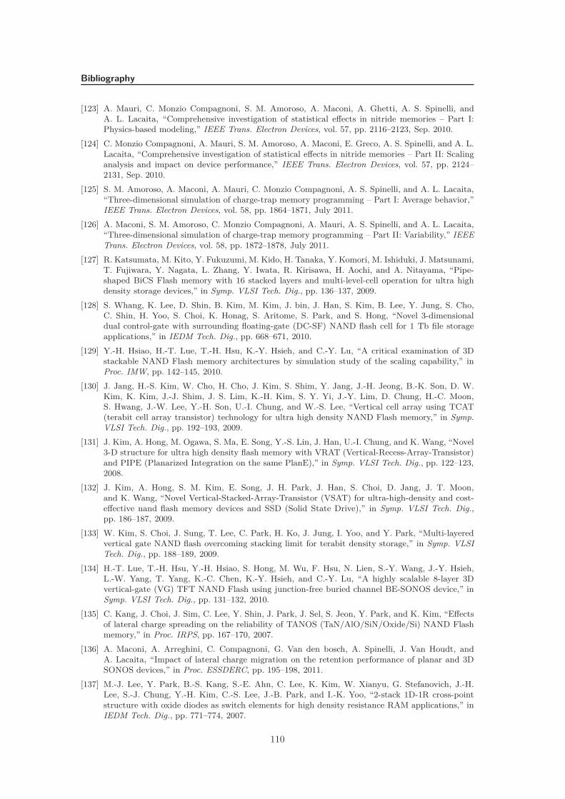
Bibliography
[123] A. Mauri, C. Monzio Compagnoni, S. M. Amoroso, A. Maconi, A. Ghetti, A. S. Spinelli, andA. L. Lacaita, “Comprehensive investigation of statistical effects in nitride memories – Part I:Physics-based modeling,” IEEE Trans. Electron Devices, vol. 57, pp. 2116–2123, Sep. 2010.
[124] C. Monzio Compagnoni, A. Mauri, S. M. Amoroso, A. Maconi, E. Greco, A. S. Spinelli, and A. L.Lacaita, “Comprehensive investigation of statistical effects in nitride memories – Part II: Scalinganalysis and impact on device performance,” IEEE Trans. Electron Devices, vol. 57, pp. 2124–2131, Sep. 2010.
[125] S. M. Amoroso, A. Maconi, A. Mauri, C. Monzio Compagnoni, A. S. Spinelli, and A. L. Lacaita,“Three-dimensional simulation of charge-trap memory programming – Part I: Average behavior,”IEEE Trans. Electron Devices, vol. 58, pp. 1864–1871, July 2011.
[126] A. Maconi, S. M. Amoroso, C. Monzio Compagnoni, A. Mauri, A. S. Spinelli, and A. L. Lacaita,“Three-dimensional simulation of charge-trap memory programming – Part II: Variability,” IEEETrans. Electron Devices, vol. 58, pp. 1872–1878, July 2011.
[127] R. Katsumata, M. Kito, Y. Fukuzumi, M. Kido, H. Tanaka, Y. Komori, M. Ishiduki, J. Matsunami,T. Fujiwara, Y. Nagata, L. Zhang, Y. Iwata, R. Kirisawa, H. Aochi, and A. Nitayama, “Pipe-shaped BiCS Flash memory with 16 stacked layers and multi-level-cell operation for ultra highdensity storage devices,” in Symp. VLSI Tech. Dig., pp. 136–137, 2009.
[128] S. Whang, K. Lee, D. Shin, B. Kim, M. Kim, J. bin, J. Han, S. Kim, B. Lee, Y. Jung, S. Cho,C. Shin, H. Yoo, S. Choi, K. Honag, S. Aritome, S. Park, and S. Hong, “Novel 3-dimensionaldual control-gate with surrounding floating-gate (DC-SF) NAND flash cell for 1 Tb file storageapplications,” in IEDM Tech. Dig., pp. 668–671, 2010.
[129] Y.-H. Hsiao, H.-T. Lue, T.-H. Hsu, K.-Y. Hsieh, and C.-Y. Lu, “A critical examination of 3Dstackable NAND Flash memory architectures by simulation study of the scaling capability,” inProc. IMW, pp. 142–145, 2010.
[130] J. Jang, H.-S. Kim, W. Cho, H. Cho, J. Kim, S. Shim, Y. Jang, J.-H. Jeong, B.-K. Son, D. W.Kim, K. Kim, J.-J. Shim, J. S. Lim, K.-H. Kim, S. Y. Yi, J.-Y. Lim, D. Chung, H.-C. Moon,S. Hwang, J.-W. Lee, Y.-H. Son, U.-I. Chung, and W.-S. Lee, “Vertical cell array using TCAT(terabit cell array transistor) technology for ultra high density NAND Flash memory,” in Symp.VLSI Tech. Dig., pp. 192–193, 2009.
[131] J. Kim, A. Hong, M. Ogawa, S. Ma, E. Song, Y.-S. Lin, J. Han, U.-I. Chung, and K. Wang, “Novel3-D structure for ultra high density flash memory with VRAT (Vertical-Recess-Array-Transistor)and PIPE (Planarized Integration on the same PlanE),” in Symp. VLSI Tech. Dig., pp. 122–123,2008.
[132] J. Kim, A. Hong, S. M. Kim, E. Song, J. H. Park, J. Han, S. Choi, D. Jang, J. T. Moon,and K. Wang, “Novel Vertical-Stacked-Array-Transistor (VSAT) for ultra-high-density and cost-effective nand flash memory devices and SSD (Solid State Drive),” in Symp. VLSI Tech. Dig.,pp. 186–187, 2009.
[133] W. Kim, S. Choi, J. Sung, T. Lee, C. Park, H. Ko, J. Jung, I. Yoo, and Y. Park, “Multi-layeredvertical gate NAND flash overcoming stacking limit for terabit density storage,” in Symp. VLSITech. Dig., pp. 188–189, 2009.
[134] H.-T. Lue, T.-H. Hsu, Y.-H. Hsiao, S. Hong, M. Wu, F. Hsu, N. Lien, S.-Y. Wang, J.-Y. Hsieh,L.-W. Yang, T. Yang, K.-C. Chen, K.-Y. Hsieh, and C.-Y. Lu, “A highly scalable 8-layer 3Dvertical-gate (VG) TFT NAND Flash using junction-free buried channel BE-SONOS device,” inSymp. VLSI Tech. Dig., pp. 131–132, 2010.
[135] C. Kang, J. Choi, J. Sim, C. Lee, Y. Shin, J. Park, J. Sel, S. Jeon, Y. Park, and K. Kim, “Effectsof lateral charge spreading on the reliability of TANOS (TaN/AlO/SiN/Oxide/Si) NAND Flashmemory,” in Proc. IRPS, pp. 167–170, 2007.
[136] A. Maconi, A. Arreghini, C. Compagnoni, G. Van den bosch, A. Spinelli, J. Van Houdt, andA. Lacaita, “Impact of lateral charge migration on the retention performance of planar and 3DSONOS devices,” in Proc. ESSDERC, pp. 195–198, 2011.
[137] M.-J. Lee, Y. Park, B.-S. Kang, S.-E. Ahn, C. Lee, K. Kim, W. Xianyu, G. Stefanovich, J.-H.Lee, S.-J. Chung, Y.-H. Kim, C.-S. Lee, J.-B. Park, and I.-K. Yoo, “2-stack 1D-1R cross-pointstructure with oxide diodes as switch elements for high density resistance RAM applications,” inIEDM Tech. Dig., pp. 771–774, 2007.
110
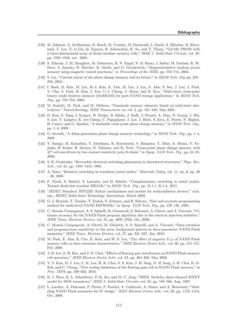
Bibliography
[138] M. Johnson, A. Al-Shamma, D. Bosch, M. Crowley, M. Farmwald, L. Fasoli, A. Ilkbahar, B. Kleve-land, T. Lee, T. yi Liu, Q. Nguyen, R. Scheuerlein, K. So, and T. Thorp, “512-Mb PROM witha three-dimensional array of diode/antifuse memory cells,” IEEE J. Solid-State Circuits, vol. 38,pp. 1920–1928, nov. 2003.
[139] S. Tehrani, J. M. Slaughter, M. Deherrera, B. N. Engel, N. D. Rizzo, J. Salter, M. Durlam, R. W.Dave, J. Janesky, B. Butcher, K. Smith, and G. Grynkewich, “Magnetoresistive random accessmemory using magnetic tunnel junctions,” in Proceedings of the IEEE, pp. 703–714, 2003.
[140] S. Lai, “Current status of the phase change memory and its future,” in IEDM Tech. Dig, pp. 255–258, 2003.
[141] I. Baek, D. Kim, M. Lee, H.-J. Kim, E. Yim, M. Lee, J. Lee, S. Ahn, S. Seo, J. Lee, J. Park,Y. Cha, S. Park, H. Kim, I. Yoo, U.-I. Chung, J. Moon, and B. Ryu, “Multi-layer cross-pointbinary oxide resistive memory (OxRRAM) for post-NAND storage application,” in IEDM Tech.Dig., pp. 750–753, 2005.
[142] M. Kozicki, M. Park, and M. Mitkova, “Nanoscale memory elements based on solid-state elec-trolytes,” Nanotechnology, IEEE Transactions on, vol. 4, pp. 331–338, May 2005.
[143] D. Kau, S. Tang, I. Karpov, R. Dodge, B. Klehn, J. Kalb, J. Strand, A. Diaz, N. Leung, J. Wu,S. Lee, T. Langtry, K. wei Chang, C. Papagianni, J. Lee, J. Hirst, S. Erra, E. Flores, N. Righos,H. Castro, and G. Spadini, “A stackable cross point phase change memory,” in IEDM Tech. Dig.,pp. 1–4, 2009.
[144] G. Servalli, “A 45nm generation phase change memory technology,” in IEDM Tech. Dig., pp. 1–4,2009.
[145] Y. Sasago, M. Kinoshita, T. Morikawa, K. Kurotsuchi, S. Hanzawa, T. Mine, A. Shima, Y. Fu-jisaki, H. Kume, H. Moriya, N. Takaura, and K. Torii, “Cross-point phase change memory with4f2 cell size driven by low-contact-resistivity poly-Si diode,” in Symp. VLSI Tech. Dig., pp. 24–25,2009.
[146] S. R. Ovshinsky, “Reversible electrical switching phenomena in disordered structures,” Phys. Rev.Lett., vol. 21, pp. 1450–1453, 1968.
[147] A. Sawa, “Resistive switching in transition metal oxides,” Materials Today, vol. 11, no. 6, pp. 28– 36, 2008.
[148] F. Nardi, S. Balatti, S. Larentis, and D. Ielmini, “Complementary switching in metal oxides:Toward diode-less crossbar RRAMs,” in IEDM Tech. Dig., pp. 31.1.1–31.1.4, 2011.
[149] “JEDEC Standard JEP122E: Failure mechanisms and models for semiconductor devices,” tech.rep., JEDEC Solid State Technology Association, March 2009.
[150] G. J. Hemink, T. Tanaka, T. Endoh, S. Aritome, and R. Shirota, “Fast and accurate programmingmethod for multi-level NAND EEPROMs,” in Symp. VLSI Tech. Dig., pp. 129–130, 1995.
[151] C. Monzio Compagnoni, A. S. Spinelli, R. Gusmeroli, S. Beltrami, A. Ghetti, and A. Visconti, “Ul-timate accuracy for the NAND Flash program algorithm due to the electron injection statistics,”IEEE Trans. Electron Devices, vol. 55, pp. 2695–2702, Oct. 2008.
[152] C. Monzio Compagnoni, A. Ghetti, M. Ghidotti, A. S. Spinelli, and A. Visconti, “Data retentionand program/erase sensitivity to the array background pattern in deca-nanometer NAND Flashmemories,” IEEE Trans. Electron Devices, vol. 57, pp. 321–327, Jan. 2010.
[153] M. Park, E. Ahn, E. Cho, K. Kim, and W.-S. Lee, “The effect of negative VT H of NAND Flashmemory cells on data retention characteristics,” IEEE Electron Device Lett., vol. 30, pp. 155–157,Feb. 2009.
[154] J.-D. Lee, S.-H. Hur, and J.-D. Choi, “Effects of floating-gate interference on NAND Flash memorycell operation,” IEEE Electron Device Lett., vol. 23, pp. 264–266, May 2002.
[155] Y. S. Kim, D. J. Lee, C. K. Lee, H. K. Choi, S. S. Kim, J. H. Song, D. H. Song, J.-H. Choi, K.-D.Suh, and C. Chung, “New scaling limitation of the floating gate cell in NAND Flash memory,” inProc. IRPS, pp. 599–603, 2010.
[156] B. J. Sheu, D. L. Scharfetter, P.-K. Ko, and M.-C. Jeng, “BSIM: Berkeley short-channel IGFETmodel for MOS transistors,” IEEE J. Solid-State Circuits, vol. 22, pp. 558–566, Aug. 1987.
[157] L. Larcher, A. Padovani, P. Pavan, P. Fantini, A. Calderoni, A. Mauri, and A. Benvenuti, “Mod-eling NAND Flash memories for IC design,” IEEE Electron Device Lett., vol. 29, pp. 1152–1154,Oct. 2008.
111
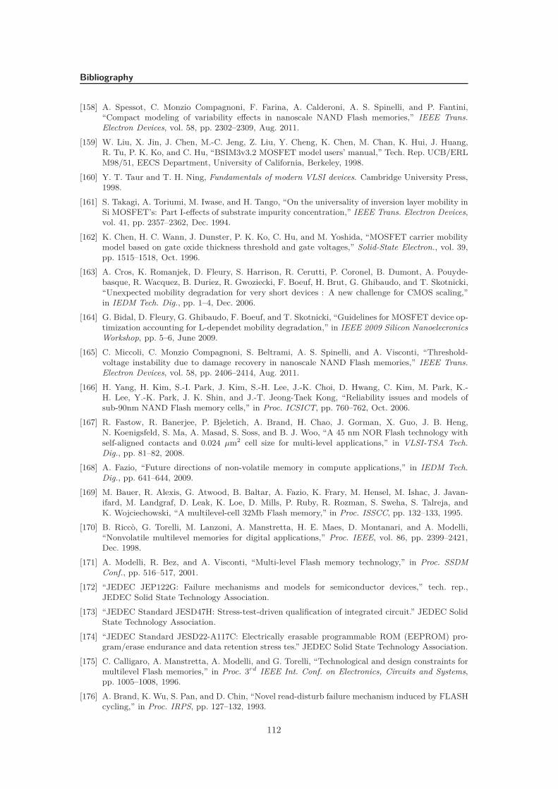
Bibliography
[158] A. Spessot, C. Monzio Compagnoni, F. Farina, A. Calderoni, A. S. Spinelli, and P. Fantini,“Compact modeling of variability effects in nanoscale NAND Flash memories,” IEEE Trans.Electron Devices, vol. 58, pp. 2302–2309, Aug. 2011.
[159] W. Liu, X. Jin, J. Chen, M.-C. Jeng, Z. Liu, Y. Cheng, K. Chen, M. Chan, K. Hui, J. Huang,R. Tu, P. K. Ko, and C. Hu, “BSIM3v3.2 MOSFET model users’ manual,” Tech. Rep. UCB/ERLM98/51, EECS Department, University of California, Berkeley, 1998.
[160] Y. T. Taur and T. H. Ning, Fundamentals of modern VLSI devices. Cambridge University Press,1998.
[161] S. Takagi, A. Toriumi, M. Iwase, and H. Tango, “On the universality of inversion layer mobility inSi MOSFET’s: Part I-effects of substrate impurity concentration,” IEEE Trans. Electron Devices,vol. 41, pp. 2357–2362, Dec. 1994.
[162] K. Chen, H. C. Wann, J. Dunster, P. K. Ko, C. Hu, and M. Yoshida, “MOSFET carrier mobilitymodel based on gate oxide thickness threshold and gate voltages,” Solid-State Electron., vol. 39,pp. 1515–1518, Oct. 1996.
[163] A. Cros, K. Romanjek, D. Fleury, S. Harrison, R. Cerutti, P. Coronel, B. Dumont, A. Pouyde-basque, R. Wacquez, B. Duriez, R. Gwoziecki, F. Boeuf, H. Brut, G. Ghibaudo, and T. Skotnicki,“Unexpected mobility degradation for very short devices : A new challenge for CMOS scaling,”in IEDM Tech. Dig., pp. 1–4, Dec. 2006.
[164] G. Bidal, D. Fleury, G. Ghibaudo, F. Boeuf, and T. Skotnicki, “Guidelines for MOSFET device op-timization accounting for L-dependet mobility degradation,” in IEEE 2009 Silicon NanoelecronicsWorkshop, pp. 5–6, June 2009.
[165] C. Miccoli, C. Monzio Compagnoni, S. Beltrami, A. S. Spinelli, and A. Visconti, “Threshold-voltage instability due to damage recovery in nanoscale NAND Flash memories,” IEEE Trans.Electron Devices, vol. 58, pp. 2406–2414, Aug. 2011.
[166] H. Yang, H. Kim, S.-I. Park, J. Kim, S.-H. Lee, J.-K. Choi, D. Hwang, C. Kim, M. Park, K.-H. Lee, Y.-K. Park, J. K. Shin, and J.-T. Jeong-Taek Kong, “Reliability issues and models ofsub-90nm NAND Flash memory cells,” in Proc. ICSICT, pp. 760–762, Oct. 2006.
[167] R. Fastow, R. Banerjee, P. Bjeletich, A. Brand, H. Chao, J. Gorman, X. Guo, J. B. Heng,N. Koenigsfeld, S. Ma, A. Masad, S. Soss, and B. J. Woo, “A 45 nm NOR Flash technology withself-aligned contacts and 0.024 µm2 cell size for multi-level applications,” in VLSI-TSA Tech.Dig., pp. 81–82, 2008.
[168] A. Fazio, “Future directions of non-volatile memory in compute applications,” in IEDM Tech.Dig., pp. 641–644, 2009.
[169] M. Bauer, R. Alexis, G. Atwood, B. Baltar, A. Fazio, K. Frary, M. Hensel, M. Ishac, J. Javan-ifard, M. Landgraf, D. Leak, K. Loe, D. Mills, P. Ruby, R. Rozman, S. Sweha, S. Talreja, andK. Wojciechowski, “A multilevel-cell 32Mb Flash memory,” in Proc. ISSCC, pp. 132–133, 1995.
[170] B. Riccò, G. Torelli, M. Lanzoni, A. Manstretta, H. E. Maes, D. Montanari, and A. Modelli,“Nonvolatile multilevel memories for digital applications,” Proc. IEEE, vol. 86, pp. 2399–2421,Dec. 1998.
[171] A. Modelli, R. Bez, and A. Visconti, “Multi-level Flash memory technology,” in Proc. SSDMConf., pp. 516–517, 2001.
[172] “JEDEC JEP122G: Failure mechanisms and models for semiconductor devices,” tech. rep.,JEDEC Solid State Technology Association.
[173] “JEDEC Standard JESD47H: Stress-test-driven qualification of integrated circuit.” JEDEC SolidState Technology Association.
[174] “JEDEC Standard JESD22-A117C: Electrically erasable programmable ROM (EEPROM) pro-gram/erase endurance and data retention stress tes.” JEDEC Solid State Technology Association.
[175] C. Calligaro, A. Manstretta, A. Modelli, and G. Torelli, “Technological and design constraints formultilevel Flash memories,” in Proc. 3rd IEEE Int. Conf. on Electronics, Circuits and Systems,pp. 1005–1008, 1996.
[176] A. Brand, K. Wu, S. Pan, and D. Chin, “Novel read-disturb failure mechanism induced by FLASHcycling,” in Proc. IRPS, pp. 127–132, 1993.
112
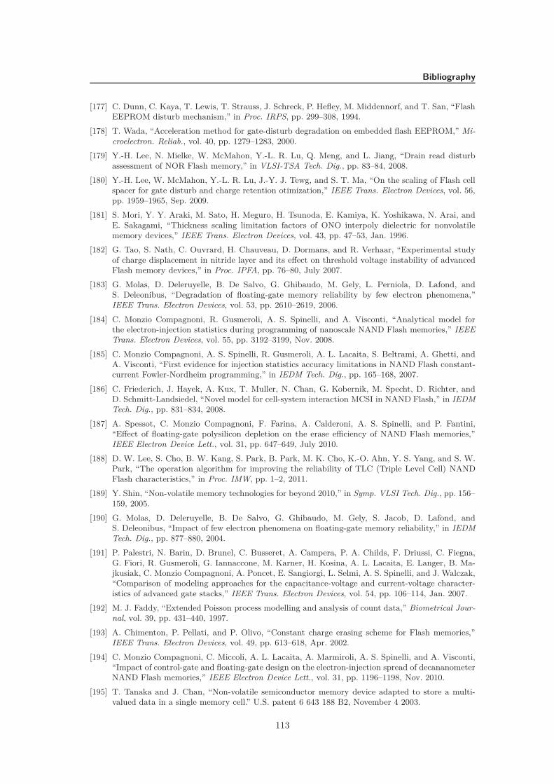
Bibliography
[177] C. Dunn, C. Kaya, T. Lewis, T. Strauss, J. Schreck, P. Hefley, M. Middennorf, and T. San, “FlashEEPROM disturb mechanism,” in Proc. IRPS, pp. 299–308, 1994.
[178] T. Wada, “Acceleration method for gate-disturb degradation on embedded flash EEPROM,” Mi-croelectron. Reliab., vol. 40, pp. 1279–1283, 2000.
[179] Y.-H. Lee, N. Mielke, W. McMahon, Y.-L. R. Lu, Q. Meng, and L. Jiang, “Drain read disturbassessment of NOR Flash memory,” in VLSI-TSA Tech. Dig., pp. 83–84, 2008.
[180] Y.-H. Lee, W. McMahon, Y.-L. R. Lu, J.-Y. J. Tewg, and S. T. Ma, “On the scaling of Flash cellspacer for gate disturb and charge retention otimization,” IEEE Trans. Electron Devices, vol. 56,pp. 1959–1965, Sep. 2009.
[181] S. Mori, Y. Y. Araki, M. Sato, H. Meguro, H. Tsunoda, E. Kamiya, K. Yoshikawa, N. Arai, andE. Sakagami, “Thickness scaling limitation factors of ONO interpoly dielectric for nonvolatilememory devices,” IEEE Trans. Electron Devices, vol. 43, pp. 47–53, Jan. 1996.
[182] G. Tao, S. Nath, C. Ouvrard, H. Chauveau, D. Dormans, and R. Verhaar, “Experimental studyof charge displacement in nitride layer and its effect on threshold voltage instability of advancedFlash memory devices,” in Proc. IPFA, pp. 76–80, July 2007.
[183] G. Molas, D. Deleruyelle, B. De Salvo, G. Ghibaudo, M. Gely, L. Perniola, D. Lafond, andS. Deleonibus, “Degradation of floating-gate memory reliability by few electron phenomena,”IEEE Trans. Electron Devices, vol. 53, pp. 2610–2619, 2006.
[184] C. Monzio Compagnoni, R. Gusmeroli, A. S. Spinelli, and A. Visconti, “Analytical model forthe electron-injection statistics during programming of nanoscale NAND Flash memories,” IEEETrans. Electron Devices, vol. 55, pp. 3192–3199, Nov. 2008.
[185] C. Monzio Compagnoni, A. S. Spinelli, R. Gusmeroli, A. L. Lacaita, S. Beltrami, A. Ghetti, andA. Visconti, “First evidence for injection statistics accuracy limitations in NAND Flash constant-current Fowler-Nordheim programming,” in IEDM Tech. Dig., pp. 165–168, 2007.
[186] C. Friederich, J. Hayek, A. Kux, T. Muller, N. Chan, G. Kobernik, M. Specht, D. Richter, andD. Schmitt-Landsiedel, “Novel model for cell-system interaction MCSI in NAND Flash,” in IEDMTech. Dig., pp. 831–834, 2008.
[187] A. Spessot, C. Monzio Compagnoni, F. Farina, A. Calderoni, A. S. Spinelli, and P. Fantini,“Effect of floating-gate polysilicon depletion on the erase efficiency of NAND Flash memories,”IEEE Electron Device Lett., vol. 31, pp. 647–649, July 2010.
[188] D. W. Lee, S. Cho, B. W. Kang, S. Park, B. Park, M. K. Cho, K.-O. Ahn, Y. S. Yang, and S. W.Park, “The operation algorithm for improving the reliability of TLC (Triple Level Cell) NANDFlash characteristics,” in Proc. IMW, pp. 1–2, 2011.
[189] Y. Shin, “Non-volatile memory technologies for beyond 2010,” in Symp. VLSI Tech. Dig., pp. 156–159, 2005.
[190] G. Molas, D. Deleruyelle, B. De Salvo, G. Ghibaudo, M. Gely, S. Jacob, D. Lafond, andS. Deleonibus, “Impact of few electron phenomena on floating-gate memory reliability,” in IEDMTech. Dig., pp. 877–880, 2004.
[191] P. Palestri, N. Barin, D. Brunel, C. Busseret, A. Campera, P. A. Childs, F. Driussi, C. Fiegna,G. Fiori, R. Gusmeroli, G. Iannaccone, M. Karner, H. Kosina, A. L. Lacaita, E. Langer, B. Ma-jkusiak, C. Monzio Compagnoni, A. Poncet, E. Sangiorgi, L. Selmi, A. S. Spinelli, and J. Walczak,“Comparison of modeling approaches for the capacitance-voltage and current-voltage character-istics of advanced gate stacks,” IEEE Trans. Electron Devices, vol. 54, pp. 106–114, Jan. 2007.
[192] M. J. Faddy, “Extended Poisson process modelling and analysis of count data,” Biometrical Jour-nal, vol. 39, pp. 431–440, 1997.
[193] A. Chimenton, P. Pellati, and P. Olivo, “Constant charge erasing scheme for Flash memories,”IEEE Trans. Electron Devices, vol. 49, pp. 613–618, Apr. 2002.
[194] C. Monzio Compagnoni, C. Miccoli, A. L. Lacaita, A. Marmiroli, A. S. Spinelli, and A. Visconti,“Impact of control-gate and floating-gate design on the electron-injection spread of decananometerNAND Flash memories,” IEEE Electron Device Lett., vol. 31, pp. 1196–1198, Nov. 2010.
[195] T. Tanaka and J. Chan, “Non-volatile semiconductor memory device adapted to store a multi-valued data in a single memory cell.” U.S. patent 6 643 188 B2, November 4 2003.
113
Bibliography
[196] V. Moschiano, G. Santin, T. Vali, and M. Rossini, “Non-volatile multilevel memory cell program-ming.” U.S. Patent 7 692 971 B2, April 6 2010.
[197] T. C. Ong, A. Fazio, N. Mielke, S. Pan, N. Righos, G. Atwood, and S. Lai, “Erratic erase inETOXT M Flash memor array,” in Symp. VLSI Tech. Dig., pp. 83–84, 1993.
[198] A. Chimenton, P. Pellati, and P. Olivo, “Analysis of erratic bits in Flash memories,” IEEE Trans.Device and Materials Reliab., vol. 4, pp. 179–184, Dec. 2001.
[199] S. Gregori, A. Cabrini, O. Khouri, and G. Torelli, “On-chip error correcting techniques for new-generation Flash memories,” Proc. IEEE, vol. 91, pp. 602–616, Apr. 2003.
[200] N. Mielke, T. Marquart, N. Wu, J. Kessenich, H. Belgal, E. Schares, F. Trivedi, E. Goodness, andL. Nevill, “Bit error rate in nand flash memories,” in Proc. IRPS, pp. 9–19, 2008.
[201] P. A. W. Lewis and G. S. Shedler, “Simulation methods for Poisson processes in nonstationarysystems,” in Proc. of the 10th conference on Winter simulation - Volume 1, pp. 155–163, 1978.
114
List of publications
1. C. Monzio Compagnoni, C. Miccoli, A. L. Lacaita, A. Marmiroli, A. S. Spinelli, A. Visconti.“Impact of the Control-Gate and Floating-Gate Design on the Electron-Injection Spread of De-cananometer NAND Flash Memories”. IEEE Electron Device Letters, vol. 31, no. 11, pp.1196–1198, Nov. 2010
2. C. Miccoli, C. Monzio Compagnoni, S. M. Amoroso, A. Spessot, P. Fantini, A. Visocnti, A. S.Spinelli. “Impact of Neutral Threshold-Voltage Spread and Electron-Emission Statistics on DataRetention of Nanoscale NAND Flash”. IEEE Electron Device Letters, vol. 31, no. 11, pp.1202–1204, Nov. 2010
3. C. Monzio Compagnoni, C. Miccoli, R. Mottadelli, S. Beltrami, M. Ghidotti, A. L. Lacaita, A. S.Spinelli, A. Visconti. “Investigation of the Threshold Voltage Instability after Distributed Cyclingin Nanoscale NAND Flash Memory Arrays”. IRPS 2010, pp. 604–610
4. C. Miccoli, C. Monzio Compagnoni, A. S. Spinelli, A. L. Lacaita. “Investigation of the Program-ming Accuracy of a Double-Verify ISPP Algorithm for Nansoscale NAND Flash Memories”. IRPS2011, pp. MY.5.1–MY.5.6
5. C. Miccoli, C. Monzio Compagnoni, S. Beltrami, A. S. Spinelli, A. Visconti. “Threshold-VoltageInstability Due to Damage Recovery in Nanoscale NAND Flash Memories”. IEEE Transactionson Electron Devices, vol. 58, no. 8, pp. 2406–2414, Aug. 2011
6. G. M. Paolucci, C. Miccoli, C. Monzio Compagnoni, L. Crespi, A. S. Spinelli, A. L. Lacaita.“Investigation of Cycling-Induced VT Instabilities in NAND Flash Cells via Compact Modeling”.IMW 2012
7. G. M. Paolucci, C. Miccoli, C. Monzio Compagnoni, A. S. Spinelli, A. L. Lacaita. “String Currentin Decananometer NAND Flash Arrays: A Compact-Modeling Investigaion”. IEEE Transactionson Electron Devices, vol. 59, no. 9, pp. 2331–2337, Sept. 2012
8. C. Miccoli, C. Monzio Compagnoni, L. Chiavarone, S. Beltrami, A. L. Lacaita, A. S. Spinelli,A. Visconti. “Assessment of Distributed-cycling Schemes on 45nm NOR Flash Memory Arrays”.IRPS 2012, pp. 2A.1.1–2A.1.7
9. C. Miccoli, J. Barber, C. Monzio Compagnoni, G. M. Paolucci, J. Kessenich, A. L. Lacaita, A.S. Spinelli, R. J. Koval, A. Goda. “Resolving Discrete Emission Events: a New Perspective forDetrapping Investigation in NAND Flash Memories”. Accepted for IRPS 2013
Awards and recognitions
[3] is cited by: “JEDEC JEP122C: Failure Mechanisms and Models for Semiconductor Devices”,tech. rep., JEDEC Solid State Technology Association, October 2011
[8] was awarded the Best Student Paper Award at the 2012 IEEE International Reliability PhysicsSymposium (IRPS), which took place from 15th to 19th of April in Anaheim (CA) - USA
115