Embed Size (px)
Citation preview
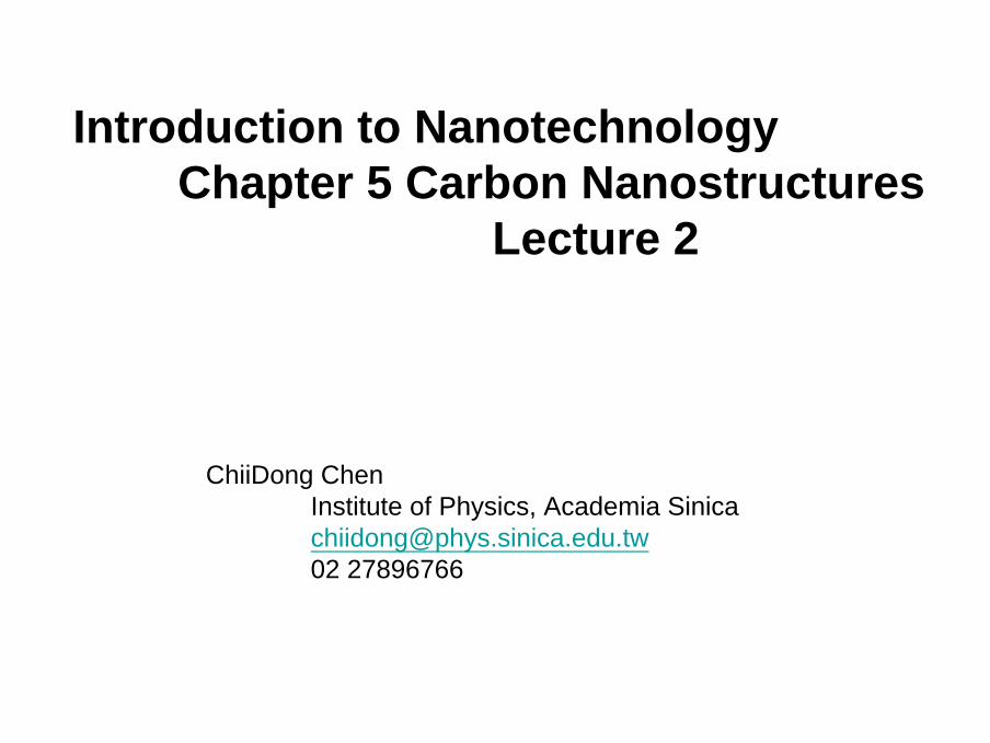
Introduction to NanotechnologyChapter 5 Carbon Nanostructures
Lecture 2
ChiiDong ChenInstitute of Physics, Academia [email protected] 27896766
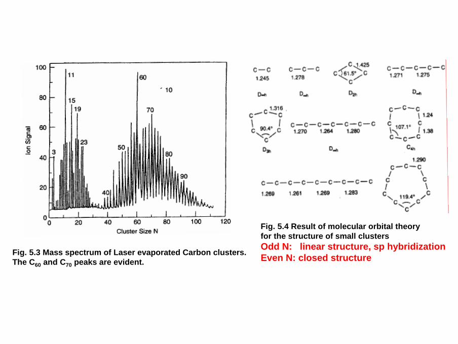
Fig. 5.3 Mass spectrum of Laser evaporated Carbon clusters. The C60 and C70 peaks are evident.
Fig. 5.4 Result of molecular orbital theory for the structure of small clustersOdd N: linear structure, sp hybridizationEven N: closed structure
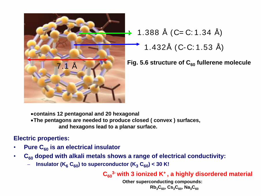
1.388 Å (C=C:1.34 Å)
1.432Å (C-C:1.53 Å)
7.1 Å Fig. 5.6 structure of C60 fullerene molecule
•contains 12 pentagonal and 20 hexagonal•The pentagons are needed to produce closed ( convex ) surfaces,
and hexagons lead to a planar surface.
Electric properties:• Pure C60 is an electrical insulator• C60 doped with alkali metals shows a range of electrical conductivity:
– Insulator (K6 C60) to superconductor (K3 C60) < 30 K!
C603- with 3 ionized K+ , a highly disordered material
Other superconducting compounds:Rb3C60, Cs3C60, Na3C60
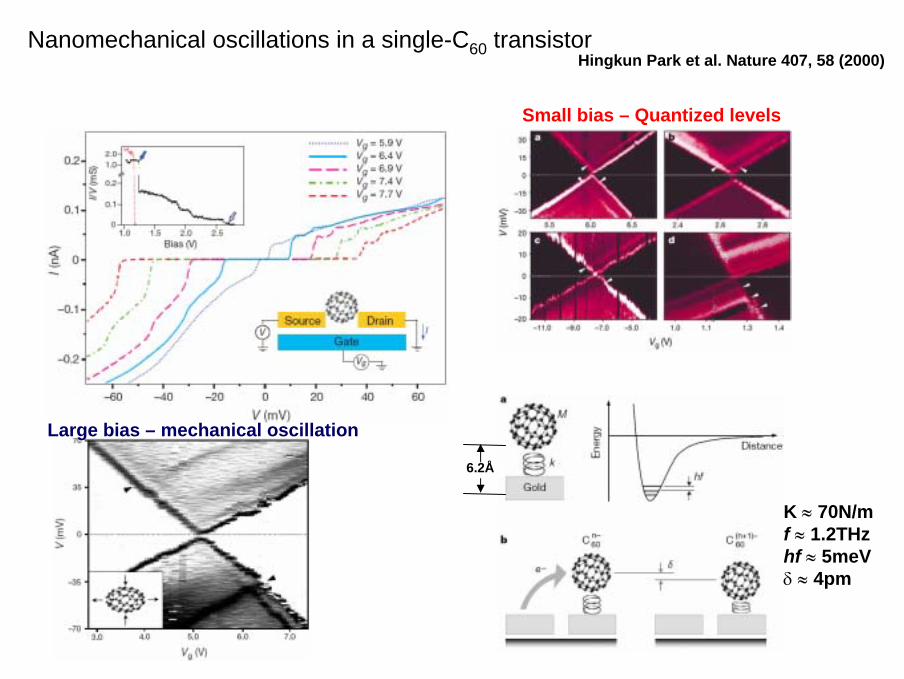
Hingkun Park et al. Nature 407, 58 (2000)Nanomechanical oscillations in a single-C60 transistor
Small bias – Quantized levels
Large bias – mechanical oscillation
6.2Å
K ≈ 70N/mf ≈ 1.2THzhf ≈ 5meVδ ≈ 4pm
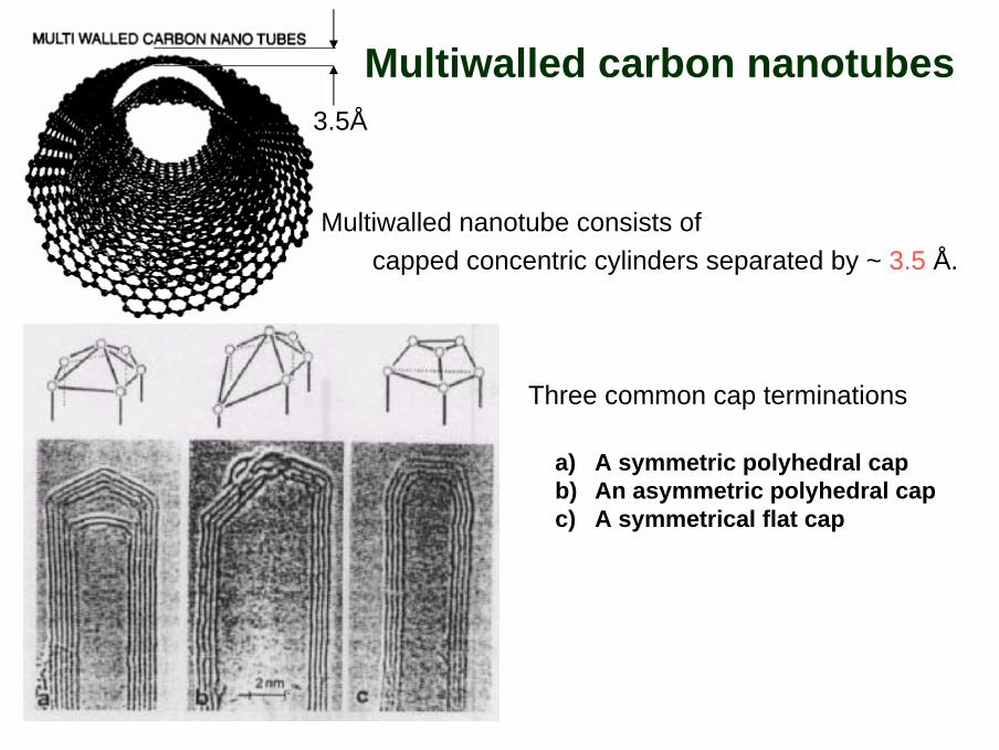
Multiwalled nanotube consists of capped concentric cylinders separated by ~ 3.5 Å.
3.5Å
a) A symmetric polyhedral capb) An asymmetric polyhedral capc) A symmetrical flat cap
Three common cap terminations
Multiwalled carbon nanotubes
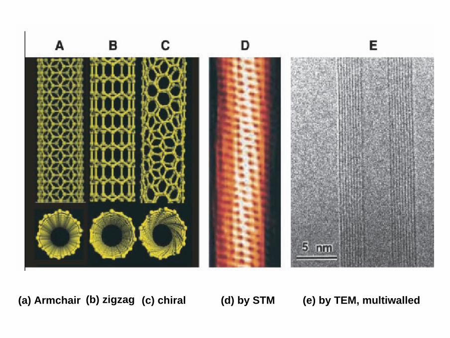
(a) Armchair (b) zigzag (c) chiral (d) by STM (e) by TEM, multiwalled
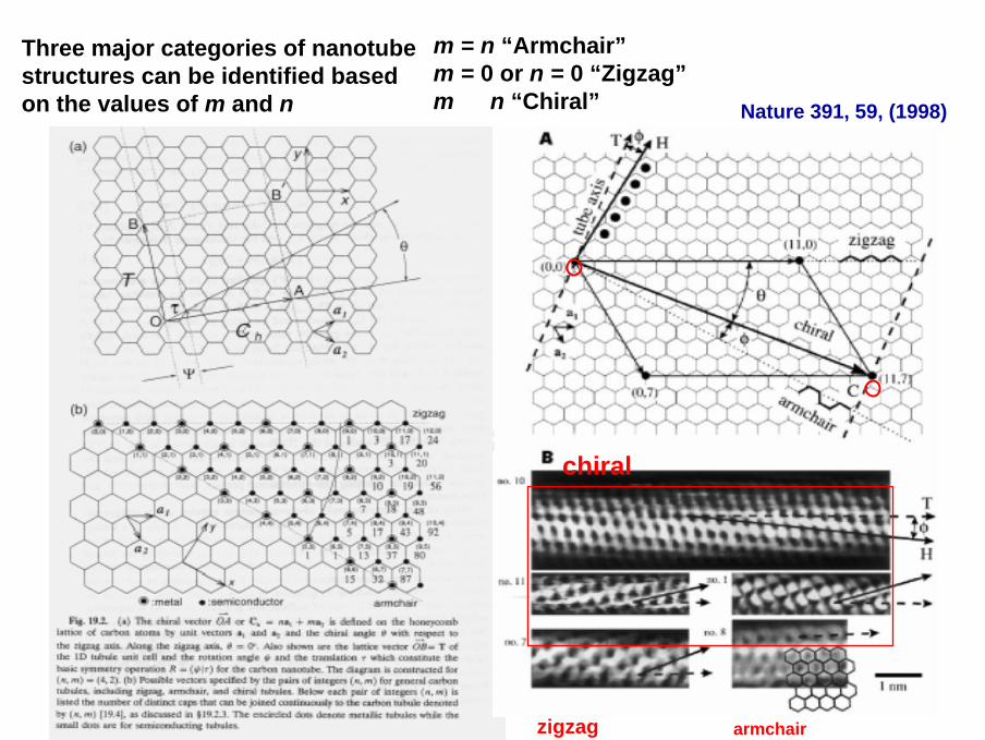
chiral
zigzag armchair
Nature 391, 59, (1998)
Three major categories of nanotube structures can be identified based on the values of m and n
m = n “Armchair”m = 0 or n = 0 “Zigzag”m ≠ n “Chiral”
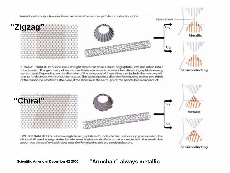
Scientific American December 62 2000
“Zigzag”
“Chiral”
“Armchair” always metallic
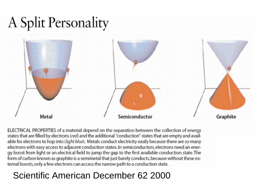
Scientific American December 62 2000
http://www.ece.eng.wayne.edu/~jchoi/06012004.pdf
nm 2
46.2 22
πmnmndCNT
++=
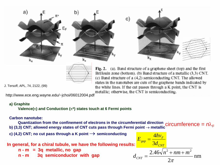
a) GraphiteValence(π) and Conduction (π*) states touch at 6 Fermi points
Carbon nanotube:Quantization from the confinement of electrons in the circumferential direction
b) (3,3) CNT; allowed energy states of CNT cuts pass through Fermi point → metallicc) (4,2) CNT; no cut pass through a K point → semiconducting
CNT
Fgap d
vE34h
=
circumference = nλF
In general, for a chiral tubule, we have the following results:n - m = 3q metallic, no gapn - m ≠ 3q semiconductor with gap
J. Tersoff, APL, 74, 2122, (99)
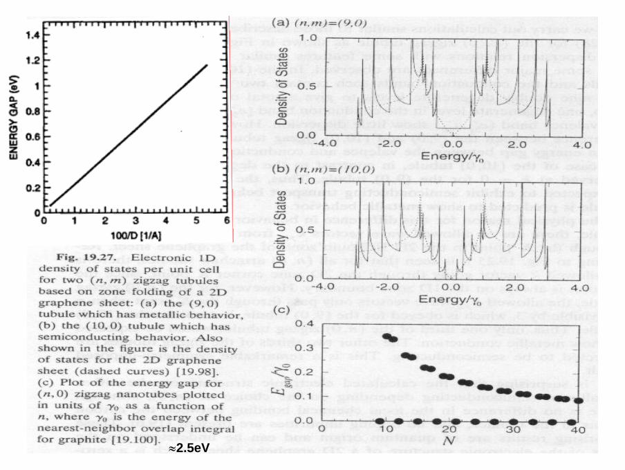
≈2.5eV
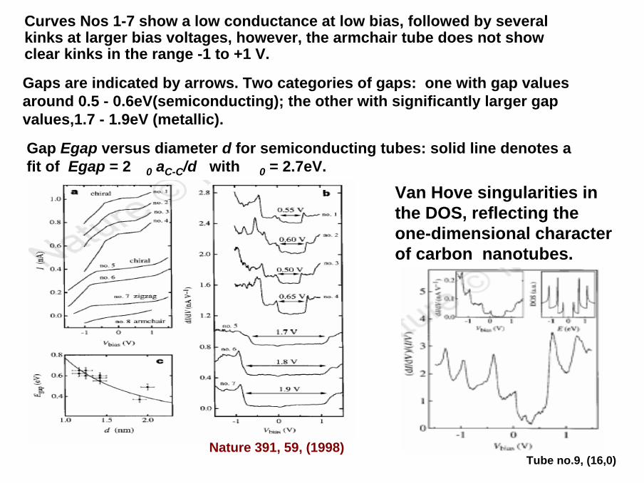
Curves Nos 1-7 show a low conductance at low bias, followed by several kinks at larger bias voltages, however, the armchair tube does not show clear kinks in the range -1 to +1 V.
Gaps are indicated by arrows. Two categories of gaps: one with gap values around 0.5 - 0.6eV(semiconducting); the other with significantly larger gap values,1.7 - 1.9eV (metallic).
Gap Egap versus diameter d for semiconducting tubes: solid line denotes a fit of Egap = 2γ0 aC-C/d with γ0 = 2.7eV.
Van Hove singularities in the DOS, reflecting the one-dimensional character of carbon nanotubes.
Tube no.9, (16,0)Nature 391, 59, (1998)
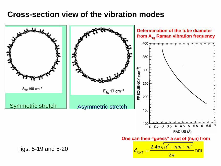
Cross-section view of the vibration modes
Symmetric stretch Asymmetric stretch
Determination of the tube diameterfrom A1g Raman vibration frequency
Figs. 5-19 and 5-20 nm 2
46.2 22
πmnmndCNT
++=
One can then “guess” a set of (m,n) from
http://www.cns.cornell.edu/documents/CornellUniversity_PN_Diode_2005_Final_1of3_000.pdf
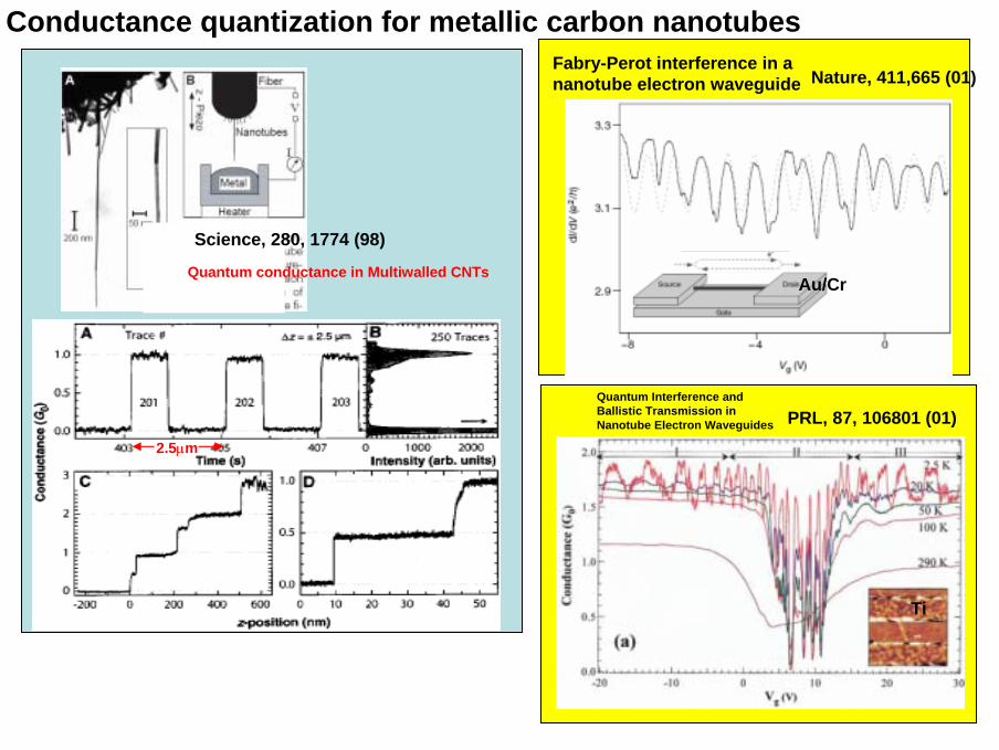
Conductance quantization for metallic carbon nanotubes
2.5µm
Science, 280, 1774 (98)
Quantum conductance in Multiwalled CNTs
Fabry-Perot interference in ananotube electron waveguide Nature, 411,665 (01)
Ti
PRL, 87, 106801 (01)Quantum Interference and Ballistic Transmission in Nanotube Electron Waveguides
Au/Cr
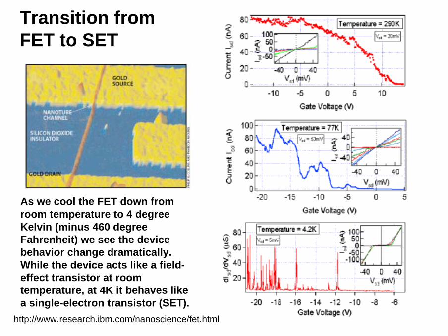
As we cool the FET down from room temperature to 4 degree Kelvin (minus 460 degree Fahrenheit) we see the device behavior change dramatically. While the device acts like a field-effect transistor at room temperature, at 4K it behaves like a single-electron transistor (SET).
Transition fromFET to SET
http://www.research.ibm.com/nanoscience/fet.html
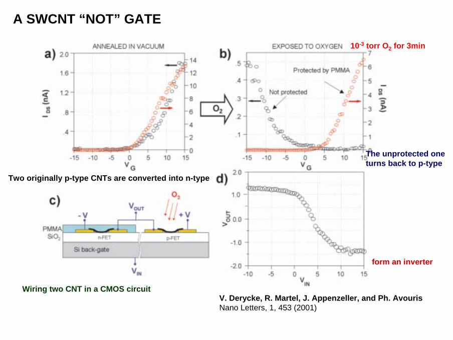
A SWCNT “NOT” GATE
Two originally p-type CNTs are converted into n-type
The unprotected one turns back to p-type
10-3 torr O2 for 3min
Wiring two CNT in a CMOS circuit
form an inverter
V. Derycke, R. Martel, J. Appenzeller, and Ph. AvourisNano Letters, 1, 453 (2001)
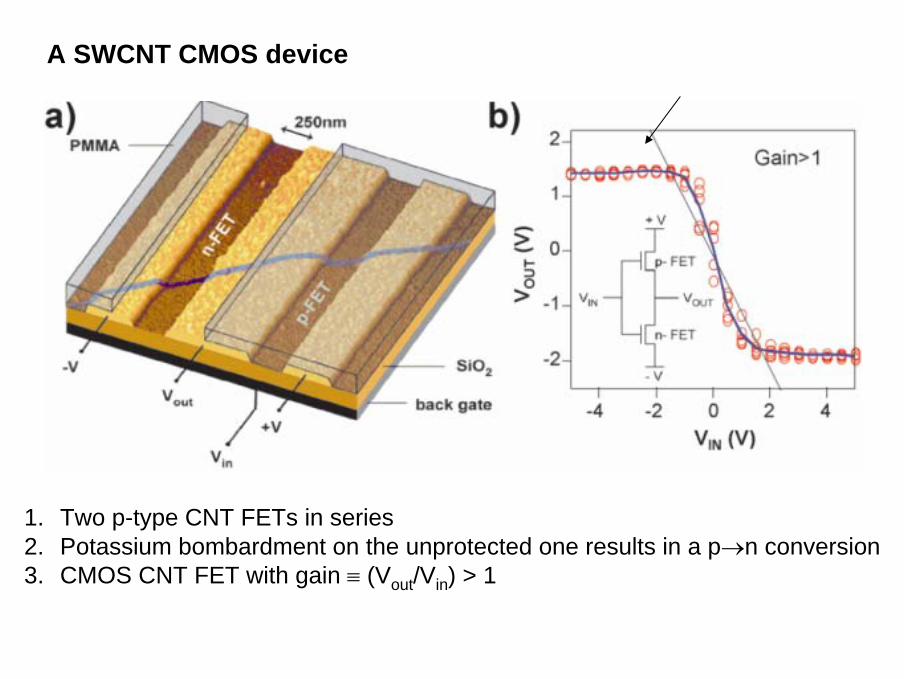
A SWCNT CMOS device
1. Two p-type CNT FETs in series2. Potassium bombardment on the unprotected one results in a p→n conversion3. CMOS CNT FET with gain ≡ (Vout/Vin) > 1
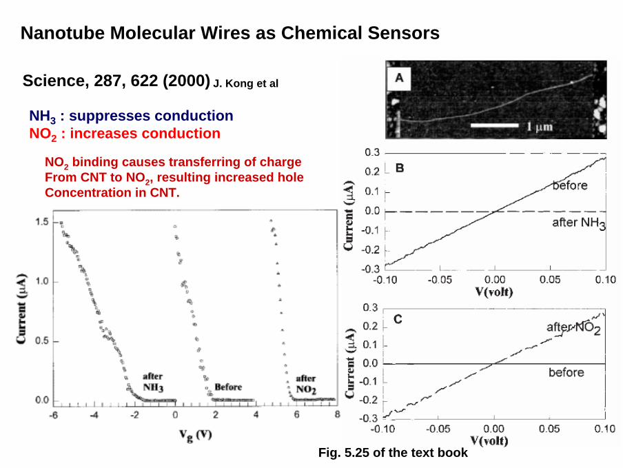
Nanotube Molecular Wires as Chemical Sensors
Fig. 5.25 of the text book
Science, 287, 622 (2000)
NO2 binding causes transferring of chargeFrom CNT to NO2, resulting increased holeConcentration in CNT.
NH3 : suppresses conductionNO2 : increases conduction
J. Kong et al
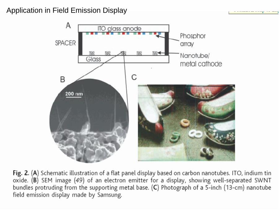
Application in Field Emission Display
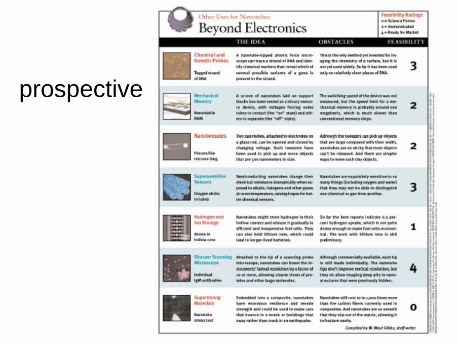
prospective
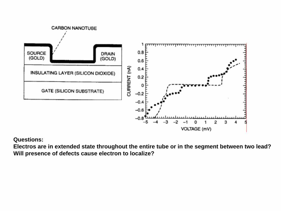
Questions:Electros are in extended state throughout the entire tube or in the segment between two lead?Will presence of defects cause electron to localize?