Embed Size (px)
Citation preview
First-Principles Study of the Electronic and MagneticProperties of Defective Carbon Nanostructures
Doctoral Thesis submitted by
Elton Jose Gomes Santos
for the degree of Doctor in Physics
June 2011
author’s e-mail: [email protected]
Ph.D Thesis
First-Principles Study of the Electronic and
Magnetic Properties of Defective Carbon
Nanostructures
Elton Jose Gomes Santos
Thesis supervisors: Daniel Sánchez Portal and Andrés Ayuela Fernández
Physics of Nanostructures and Advanced Materials, Department of Materials
Science, University of Basque Country
July 2011

© Servicio Editorial de la Universidad del País Vasco Euskal Herriko Unibertsitateko Argitalpen ZerbitzuaISBN: 978-84-695-1245-6

To Gurea and our extended family

Perhaps I can best describe my experienceof doing mathematics in terms of a journeythrough a dark unexplored mansion. Youenter the first room of the mansion and it’scompletely dark. You stumble around bumpinginto the furniture, but gradually you learnwhere each piece of furniture is. Finally,after six months or so, you find the lightswitch, you turn it on, and suddenly it’s allilluminated. You can see exactly where youwere. Then you move into the next room andspend another six months in the dark. Soeach of these breakthroughs, while sometimesthey’re momentary, sometimes over a periodof a day or two, they are the culmination of -and couldn’t exist without - the many months ofstumbling around in the dark that precede them.
- Sir Andrew John Wiles
Faster, stronger, higher. You need to improvealways.
- An olympic games proverb

6
Acknowledgements
The work presented in this Ph.D thesis was made possible by support of the Physics of Nanos-tructures and Advanced Materials Group at the Donostia International Physics Center (DIPC)and Centro Mixto CSIC-UPV/EHU (CFM), under the supervision of Prof. Pedro MiguelEchenique Landiribar. Many other colleagues in the group have greatly contributed to mywork and enriched my life. Words are not enough to express my gratitude of all the memo-rable moments of my stay in DIPC and CFM. I would like to extend my sincere gratitude toall those that had given me a helpful hand in the past 4,5 years. Among them, I am especiallygrateful to:
My supervisors Daniel Sánchez Portal and Andrés Ayuela Fernández for their supervisionsand scientific guidance. I would like to thank them for their support, encouragement, insight,hand-to-hand education and advices, as well as for their extensive feedback on my manuscriptsand presentations. They always allowed me to pursue my own ideas and treated me, since thevery first day on the same footing as a collaborator, listening to my suggestions and ideas, andhaving confidence in my potential. It has been a great pleasure and inspiration to work withyou!
Pedro Miguel Echenique Landiribar, for his support and always present scientific view ofthe life. I am very grateful to him for sharing his wide physics wisdom with me during myfirst years in the Ph.D study as well as his good advices. I truly admire his optimism andpermanent positive attitude which represented to me a vast source of motivation and energy tokeep on track.
Mads Brandbyge, for his hospitality at my stays at Technical University of Denmark(DTU), fall 2009 and spring 2010, and for his endless energy for doing fruitful and inspir-ing comments. I very much enjoyed the pleasant working environment at DTU and the manyhours expend in the "theory room 022" in weekends, holidays, etc, either alone or in the nicecompany of Mads Engelund, Jing Tao Lu, Joachim Alexander Fürst, Tue Gunst. I thank MadsBrandbyge not only for the privileged opportunity to work in his group but also for discoveringsuch a kind and friendly person. I would like also to thank Prof. Antti-Pekka Jauho at DTUfor the introduction about transport methods and Green’s function formalism. His valuablecourse has given me the right tools to treat many problems in theoretical electronics as well asin scattering process.
The DIPC and CFM staff, Ana López de Goicoechea, Marimar Alvarez, Amaia Etxaburu,Txomin Romero Asturiano, Belen Isla, Carmen Martin, Luz Fernandez, Elixabete Mendiz-abal Ituarte, Maria Formoso Ferreiro, Karmela Alonso Arreche, Iñigo Aldazabal Mensa andTimoteo Horcajo (In memoriam), for making everything to work so fluently.
Sampsa Juhana Riikonen who helped me a lot in my first years with the SIESTA methodand to understand the real life of a PhD student. Thank you for the many excursions that we
7
8
did together and for the friendship that remains so far.Some people in the Physics of Nanostructures and Advanced Materials Group for shar-
ing with me their time, experiences and for offering a pleasant working environment. Theyare Ricardo Díez Muiño, Andrés Arnau Pino, Javier Aizpurua, Iñaki Juaristi, Maite Alducin,Sebastian Bergeret, Eugene Chulkov, Ivo souza, Enrique Ortega, Vyacheslav Silkin, AngelAlegria, Lucia Vitali and Thomas Frederiksen. A special thank you goes to Thomas Frederik-sen with whom I have had a lot of fun times and discussions about the TranSiesta code.
My beloved parents, Gomes and Letice, in the far away Brazil. For the constant support,to believe in my dreams all the time and to teach me how to think like a winner. I love you!
A person that for many days, nights, weekends and holidays of calculations, literature re-search, writing and rewriting articles, preparation of talks or meetings, etc, always has beenwith me. My sincerely thank you to my lovely wife Gurea. Definitely, without her encourage-ment, motivation, support, huge patience and trust this work would not have been possible.She has been my muse and a never ending source of inspiration, whom that has given me thestrength and confidence to go forward and win the day-to-day battles. Life would not be thesame as meaningful with her out!
Our extended family, Malkoa Zarandona Porras, Zuriñe Zarandona Porras, Felipe Otaño,Eliazar Porras, Kelyane Gomes, Marcos Gerser, Keyla Gomes, Alysson Correia, Ana Leticie,Matheus Gomes, Bat and Waity. For many moments together and for your love.
Finally, but not least, our friends, Txeffo, Lus, Angeloso, Carlos, Igor, Sergio, Patri, Maria,Leire, Yaiza, for enjoyable fun moments, Caminos de Santiago, excursions, dinners, lunchs,parties, bike trips, etc, or for just being there when you need.
Elton J. G. Santos,Donostia-San Sebastián, August 16th 2011
Contents
1 Introduction 131.1 Carbon . . . . . . . . . . . . . . . . . . . . . . . . . . . . . . . . . . . . . . 131.2 Carbon and its allotropes . . . . . . . . . . . . . . . . . . . . . . . . . . . . 141.3 Electronic Structure . . . . . . . . . . . . . . . . . . . . . . . . . . . . . . . 16
1.3.1 Graphene . . . . . . . . . . . . . . . . . . . . . . . . . . . . . . . . 161.3.2 Carbon Nanotubes . . . . . . . . . . . . . . . . . . . . . . . . . . . 21
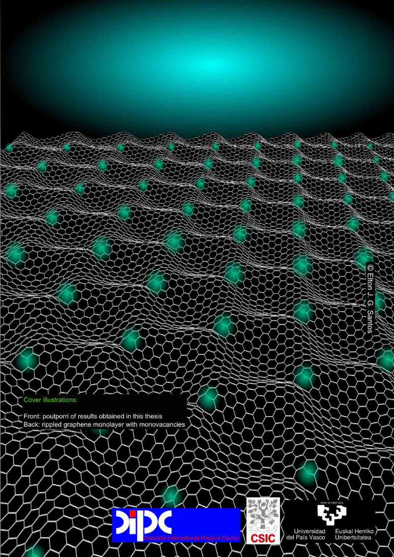
1.4 Structural properties . . . . . . . . . . . . . . . . . . . . . . . . . . . . . . . 231.4.1 Graphene as a two-dimensional crystal . . . . . . . . . . . . . . . . 231.4.2 Ripples at free-standing graphene . . . . . . . . . . . . . . . . . . . 25
1.5 Magnetism in Carbon-Based Materials . . . . . . . . . . . . . . . . . . . . . 261.5.1 Radiation-induced defect formation and ferromagnetism . . . . . . . 26
1.6 Vacancy-induced magnetism . . . . . . . . . . . . . . . . . . . . . . . . . . 281.6.1 π−Vacancy . . . . . . . . . . . . . . . . . . . . . . . . . . . . . . . 281.6.2 Real carbon vacancy . . . . . . . . . . . . . . . . . . . . . . . . . . 30
1.7 Impurities in graphene . . . . . . . . . . . . . . . . . . . . . . . . . . . . . 331.7.1 H atoms chemisorbed on graphene . . . . . . . . . . . . . . . . . . . 351.7.2 Molecular adsorption on graphene and carbon nanotubes . . . . . . . 361.7.3 Graphene and carbon nanotubes with substitutional transition metals . 38
1.8 Thesis outline . . . . . . . . . . . . . . . . . . . . . . . . . . . . . . . . . . 41
2 Electronic Structure Methods 432.1 Density Functional Theory . . . . . . . . . . . . . . . . . . . . . . . . . . . 43
2.1.1 The many-body problem . . . . . . . . . . . . . . . . . . . . . . . . 432.1.2 Foundations of the Density Functional Theory . . . . . . . . . . . . 442.1.3 Kohn-Sham formulation . . . . . . . . . . . . . . . . . . . . . . . . 45
2.2 The SIESTA method . . . . . . . . . . . . . . . . . . . . . . . . . . . . . . . 472.2.1 Periodic boundary condition . . . . . . . . . . . . . . . . . . . . . . 472.2.2 Pseudopotentials . . . . . . . . . . . . . . . . . . . . . . . . . . . . 492.2.3 Basis set . . . . . . . . . . . . . . . . . . . . . . . . . . . . . . . . 49
2.3 Convergence of Parameters . . . . . . . . . . . . . . . . . . . . . . . . . . . 502.3.1 K point sampling and smearing of the electronic occupation . . . . . 502.3.2 Pseudopotentials and basis orbital radii . . . . . . . . . . . . . . . . 522.3.3 Benchmark systems: transition metals in bulk phases and graphene . 55
9
10 Contents
3 Substitutional Metallic Impurities in Graphene: Structural, Electronic and Mag-netic Properties 593.1 The main properties of substitutional transition metals in graphene . . . . . . 59
3.1.1 Geometry and structural parameters . . . . . . . . . . . . . . . . . . 593.1.2 Binding energies . . . . . . . . . . . . . . . . . . . . . . . . . . . . 613.1.3 Spin moments . . . . . . . . . . . . . . . . . . . . . . . . . . . . . 61
3.2 Unreconstructed D3h carbon vacancy . . . . . . . . . . . . . . . . . . . . . . 653.3 Analysis of the electronic structure . . . . . . . . . . . . . . . . . . . . . . . 66
3.3.1 Sc and Ti: filling the vacancy-metal bonding levels . . . . . . . . . . 663.3.2 V, Cr and Mn: 3d magnetism . . . . . . . . . . . . . . . . . . . . . . 683.3.3 Fe, Co, Ni: strong contribution from the carbon vacancy levels . . . . 723.3.4 Noble metals . . . . . . . . . . . . . . . . . . . . . . . . . . . . . . 76
3.4 Jahn-Teller distortion of substitutional Zn . . . . . . . . . . . . . . . . . . . 783.5 Fe substitutionals: competition between intra-atomic interactions and metal-
carbon hybridization . . . . . . . . . . . . . . . . . . . . . . . . . . . . . . 793.5.1 Key parameters: metal-carbon hopping and intra-atomic Coulomb
interactions . . . . . . . . . . . . . . . . . . . . . . . . . . . . . . . 813.5.2 Relevance for recent experiments of Fe implantation in graphite . . . 84
3.6 Conclusions . . . . . . . . . . . . . . . . . . . . . . . . . . . . . . . . . . . 84
4 Real Systems that Behave Like π-Vacancies: Co Doping and Covalent Function-alization 874.1 Co substitutional impurities in graphene: Realization of single π-vacancies . 884.2 Organic adsorbates chemisorbed on graphene: Universal spin moment . . . . 90
4.2.1 Geometry and structural parameters . . . . . . . . . . . . . . . . . . 904.2.2 Spin polarization and electronic structure . . . . . . . . . . . . . . . 90
4.3 Sidewall spin functionalization in carbon nanotubes . . . . . . . . . . . . . . 954.4 Magnetic coupling between defects in graphene . . . . . . . . . . . . . . . . 96
4.4.1 Co impurities in graphitic carbon . . . . . . . . . . . . . . . . . . . 964.4.2 Chemisorbed molecules in graphene . . . . . . . . . . . . . . . . . . 1004.4.3 Adsorbates in nanotubes . . . . . . . . . . . . . . . . . . . . . . . . 102
4.5 Conclusions . . . . . . . . . . . . . . . . . . . . . . . . . . . . . . . . . . . 102
5 Effect of Strain on the Electronic and Magnetic Properties of Defects in CarbonNanostructures 1055.1 A general spin-strain phase diagram for a monovacancy in graphene . . . . . 106
5.1.1 Structure versus strain . . . . . . . . . . . . . . . . . . . . . . . . . 1065.1.2 Energetics . . . . . . . . . . . . . . . . . . . . . . . . . . . . . . . . 1085.1.3 Magnetism versus strain: several spin solutions . . . . . . . . . . . . 108
5.2 Ni doped graphene and carbon nanotubes . . . . . . . . . . . . . . . . . . . 1115.2.1 Geometry and magnetization density . . . . . . . . . . . . . . . . . . 1125.2.2 Electronic structure of Nisub impurities in graphene and nanotubes . . 1125.2.3 Oscillations of the spin moment . . . . . . . . . . . . . . . . . . . . 114
5.3 Uniaxial strain in Ni doped graphene . . . . . . . . . . . . . . . . . . . . . . 1165.3.1 Effect of uniaxial strain on the spin moment . . . . . . . . . . . . . . 1165.3.2 Electronic structure of Nisub defects under strain . . . . . . . . . . . 118

Contents 11
5.3.3 Magnetization density and an experiment proposal . . . . . . . . . . 1195.4 Conclusions . . . . . . . . . . . . . . . . . . . . . . . . . . . . . . . . . . . 120
6 Summary and outlook 1256.1 Outlook . . . . . . . . . . . . . . . . . . . . . . . . . . . . . . . . . . . . . 128
A Publications 131
B Conference and Workshop Contributions 133

12 Contents
Chapter 1
Introduction
This chapter serves to put into context the results presented in this thesis. We point out the im-portance of carbon nanostructures on today’s science and technology. We give a brief overviewon their structural and electronic properties. We start by presenting the graphene layer in 2Dand it is followed by carbon nanotubes where the layer is rolled up into a quasi-1D structure.The electronic and scattering properties are affected by defects such as impurities and adsor-bates, which can also generate magnetism. Finally the outline of the remaining part of thethesis is given.
1.1 Carbon
"Life exists in the universe only because the carbon atom possesses certain exceptional prop-erties". Even said long time ago by Sir James Jeans, this sentence still contains an enormousamount of information about carbon if just some imagination and thinking are applied. Dur-ing the industrial revolution in 19th century, carbon became one of the key elements for thedevelopment of new technologies in the modern world (railway, steel, chemical industries,etc). Nowadays, carbon is expected to be determinant for the next technological revolutioncoming soon. Like Silicon in the 20th century, which allowed the semiconductor industry todevelop the current high performance electronics in less than eighty years, the hopes are thatcarbon and its new allotropes will allow for a similar development in a much shorter periodof time. The reasons to look for alternatives to Silicon are that its physical characteristicsthat are useful for electronics will reach their limits in the nearly future [1]. For instance, theComplementary Metal-Oxide Semiconductor (CMOS) transistor would be close to its funda-mental limits of a charge-based switch around 2024. In the meantime, it has become custom tochange our notebook, digital camera, mobile phone, etc for a faster and better updated versionat a timescale ranging from months to a few years. Therefore, other alternatives should beconsidered to process the ever increasing amount of data and information that nowadays liferequires. The alternative in this context is to go to a nanometer scale or to a nanotechnologyapproach which has the carbon nanostructures as a model for new advances [2].
In his famous speech "There is plenty of room at the bottom" [3], Feynmann predicted thedirect manipulation on the atomic scale as the novel challenge to be faced by the scientificcommunity. In particular, he thought about the possibility of making electronic componentson this lenght scale. The realization hereof can be boiled down to Moore’s law which states
13
14 Chapter 1. Introduction
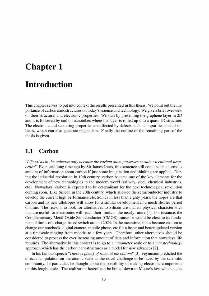
that the transistor density on integrated circuits (IC) doubles every two years [4]. As pointedout in the Los Angeles Times, if the same rate of performance improvement versus cost heldfor airlines, a flight from New York to Paris would cost one cent and will take less than asecond. This has been made possible by the great advances in lithography which allowedever denser and more complex IC. In agreement with Moore, IC and scaling are "the cheapway to do electronics" [5]. Even with large increases in lithography tool cost to fabricatemicroscale silicon-based transistors, the cost per transistor has decreased by many orders ofmagnitude during the last forty years. Conversely, at the same period of time, the cost oflithography equipment increased from $10,000 to $35 millions as shown in Figure 1.1 andis likely to remain increasing in the next near future. Nevertheless, this device scaling andperformance enhancement can not continue forever. A number of limitations of fundamentalscientific as well as technological nature place limits on the ultimate size and performance ofsilicon devices. This calls for new approaches such as the use of carbon nanomaterials as thekey components of the device (e.g. conducting channel), for which the term carbon electron-ics has been coined. There are many reasons that highlight the role of carbon nanomaterialsas the next paradigm for Moore’s law. To cite some of them: Temperature tolerance andstability, carbon has higher thermal conductivity than conventional CMOS structures whichcould improve the operation temperature reducing it considerably; Speed, in the recently dis-covered graphene, electrons and holes can move through its structure ballistically, travellingfor micrometers up to 2000 times faster than in silicon; Size , carbon nanostructures have thepotential to dramatically extend the miniaturisation that has driven the density and speed ad-vantages of the IC phase of Moore’s law; Power, at the very small size scales needed to createever denser device arrays, silicon generates too much resistance to electron flow, creating moreheat than can be dissipated and consuming too much power. On the other hand, graphene, forinstance, has no such restrictions [6]. Thus, these emerging carbon-based materials seem tooffer new possibilities for future technologies that go beyond those of the CMOS applications.In the following sections we study some of the carbon nanostructures giving more details ontheir electronic and structural properties.
1.2 Carbon and its allotropes
Carbon exists in many allotropic forms. This is a signature of the very rich chemistry ofcarbon, the central materials for life on earth. Recently, some of the carbon allotropes haveattracted a large amount of research and interest. This is partly driven by the promise of newtechnological applications, some of which have been already demonstrated in the laboratories.To cite some carbon allotropes, the sp2 (graphene, nanotubes, fullerenes) and sp3 (diamond)hybridised carbon networks are of particular interest because they have remarkable proper-ties compared to other materials. Some of these properties include high hardness, mechanicalresistance, resistance to radiation damage, anomalous quantum Hall effect, excellent thermalconductivity, biocompatibility and superconductivity. The recent discovered graphene, for ex-ample, has uncommon electronic and transport properties such as a high carrier mobility. Theelectrons in graphene can move without collisions over great distances, even at room temper-ature. Consequently, graphene has the ability to conduct electrical currents 10 to 100 timesgreater than conventional silicon-based semiconductors with very small head dissipation. Inparticular, this is one of the many features that makes graphene a promising candidate for
1.2. Carbon and its allotropes 15
Figure 1.1: Lithography tool cost and transistor cost versus years. Reproduced from Ref. [5].
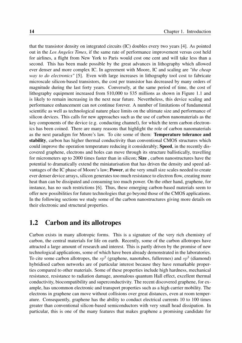
future electronic applications and has attracted a great interest in science and technology re-search. The number of papers in this field is growing exponentially as shown in Figure 1.2.The field has already two Nobel prizes: one in chemistry given to Curl, Kroto and Smalley in1996 "for the discovery of fullerenes"; and another in physics, to Geim and Novoselov in 2010"for groundbreaking experiments regarding the two-dimensional material graphene"; and stillwaiting for the third one in nanotubes (Iijima and Bethune?); this research community doesnot seem to stop growing up for the next few years and beyond. Furthermore, part of thisgrowth is reflected by an acceleration of the increase in the upward slope of the number ofpublication of the graphene curve as shown in Figure 1.2 and in the number of researchersthat are entering the field. It is also noteworthy that although the nanocarbon community hadgrown rapidly from the discovery of fullerenes in 1985, and later by nanotube-based researchin 1991, graphene itself did not attract much attention until the 2004 publications of Geim andNovoselov [7].
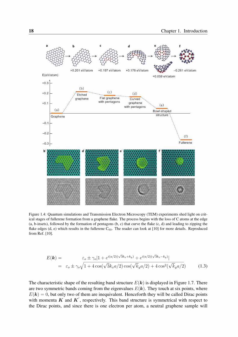
The concept of graphene has been around for a long time since 1947 when P. R. Wallacepublished the first tight-binding model for a single graphite sheet [9]. He showed the un-usual semimetallic behavior in this material and obtained the linear E(k) dispersion aroundthe K point of the Brillouin zone. However, at that time the interest in carbon nanostructureswas minuscule and the only carbon material that had some relevance was graphite. In theyears following Wallace’s paper, graphene played an important role since it made the theo-retical framework for understanding the electronic structure of other carbon allotropes thatwere progressively discovered (see Figure 1.3). For instance, fullerenes can be generatedfrom graphene by introducting pentagons that create positive curvature defects, and hence,
16 Chapter 1. Introduction
Figure 1.2: Record of publications from ISI Web of Knowledge with "carbon nanotube(s)" or "graphene(s)"or "fullerene(s)" in the topic. Insets from: The Nobel Foundation (nobelprize.org), Microscopy Societyof America (www.microscopy.org), Metrolic (www.metrolic.com), NANOid (www.nanoid.co.uk), and IBM(domino.research.ibm.com).
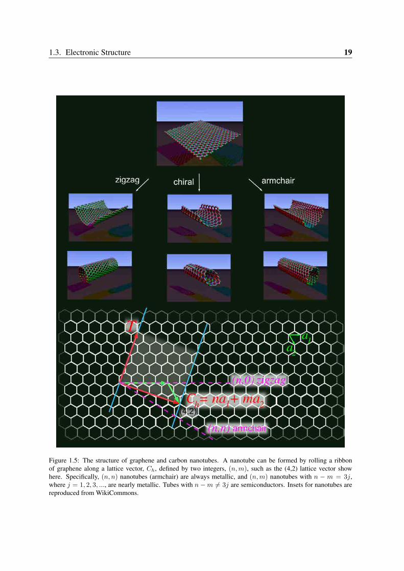
fullerenes can be thought as a 0D nanocarbon. Although this idea seems to be simple, theexperimental route to form these carbon cages from a flat graphene sheet is still a topic ofresearch [10,11]. Fullerene formation is based on four critical steps in a top-down mechanismstarting from graphene flakes as is seen in Figure 1.4. Carbon nanotubes, in its turn, are ob-tained by rolling graphene along certain directions and connecting the carbon bonds as shownin Figure 1.5. Thus carbon nanotubes have only hexagons and can be thought as a 1D.
In the following, we shall describe the main properties of graphene and carbon nanotubes(CNT) with the focus on the electronic and structural features that will be important for thisthesis.
1.3 Electronic Structure
1.3.1 Graphene
The peculiar electronic structure of graphene allows us to understand the quantum propertiesof other carbon nanostructures. The band structure of graphene at low energies, was firstdeduced by Wallace in 1947 [9] and can analytically be obtained within the π-orbital tight-binding approximation. This approximation treats just the pz electron in each C atom asthe main state relevant for describing the full electronic structure. C possesses four valenceelectrons, three of them form covalent σ bonds with the neighbours in the plane, and the fourth
1.3. Electronic Structure 17
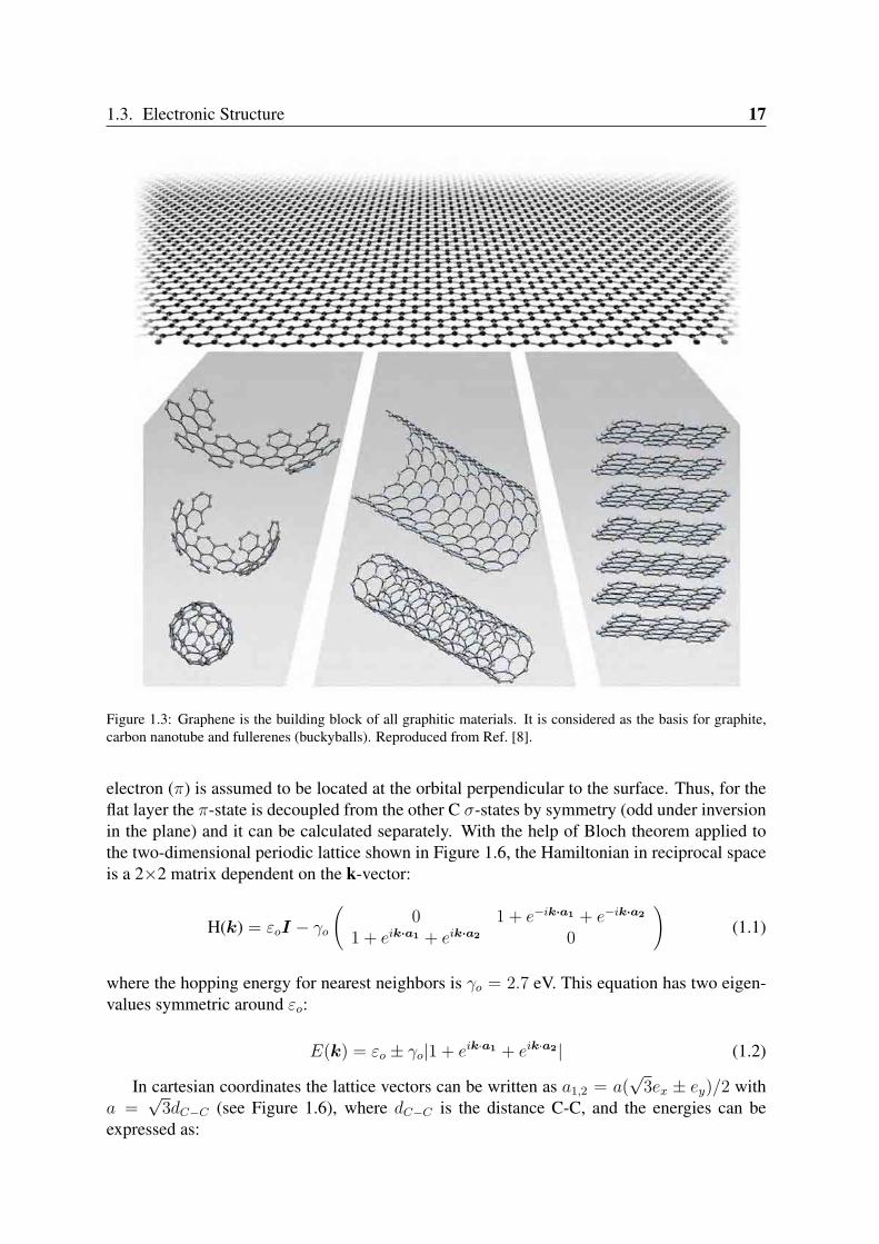
Figure 1.3: Graphene is the building block of all graphitic materials. It is considered as the basis for graphite,carbon nanotube and fullerenes (buckyballs). Reproduced from Ref. [8].
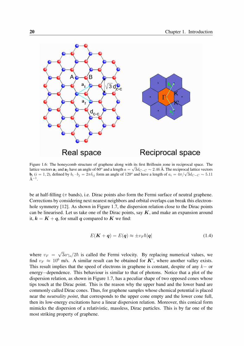
electron (π) is assumed to be located at the orbital perpendicular to the surface. Thus, for theflat layer the π-state is decoupled from the other C σ-states by symmetry (odd under inversionin the plane) and it can be calculated separately. With the help of Bloch theorem applied tothe two-dimensional periodic lattice shown in Figure 1.6, the Hamiltonian in reciprocal spaceis a 2×2 matrix dependent on the k-vector:
H(k) = εoI − γo
(0 1 + e−ik·a1 + e−ik·a2
1 + eik·a1 + eik·a2 0
)(1.1)
where the hopping energy for nearest neighbors is γo = 2.7 eV. This equation has two eigen-values symmetric around εo:
E(k) = εo ± γo|1 + eik·a1 + eik·a2| (1.2)
In cartesian coordinates the lattice vectors can be written as a1,2 = a(√
3ex ± ey)/2 witha =
√3dC−C (see Figure 1.6), where dC−C is the distance C-C, and the energies can be
expressed as:
18 Chapter 1. Introduction
Figure 1.4: Quantum simulations and Transmission Electron Microscopy (TEM) experiments shed light on crit-ical stages of fullerene formation from a graphene flake. The process begins with the loss of C atoms at the edge(a, b-insets), followed by the formation of pentagons (b, c) that curve the flake (c, d) and leading to zipping theflake edges (d, e) which results in the fullerene C60. The reader can look at [10] for more details. Reproducedfrom Ref. [10].
E(k) = εo ± γo|1 + ei(a/2)(√
3kx+ky) + ei(a/2)(√
3kx−ky)|
= εo ± γo
√1 + 4 cos(
√3kxa/2) cos(
√kya/2) + 4 cos2(
√kya/2) (1.3)
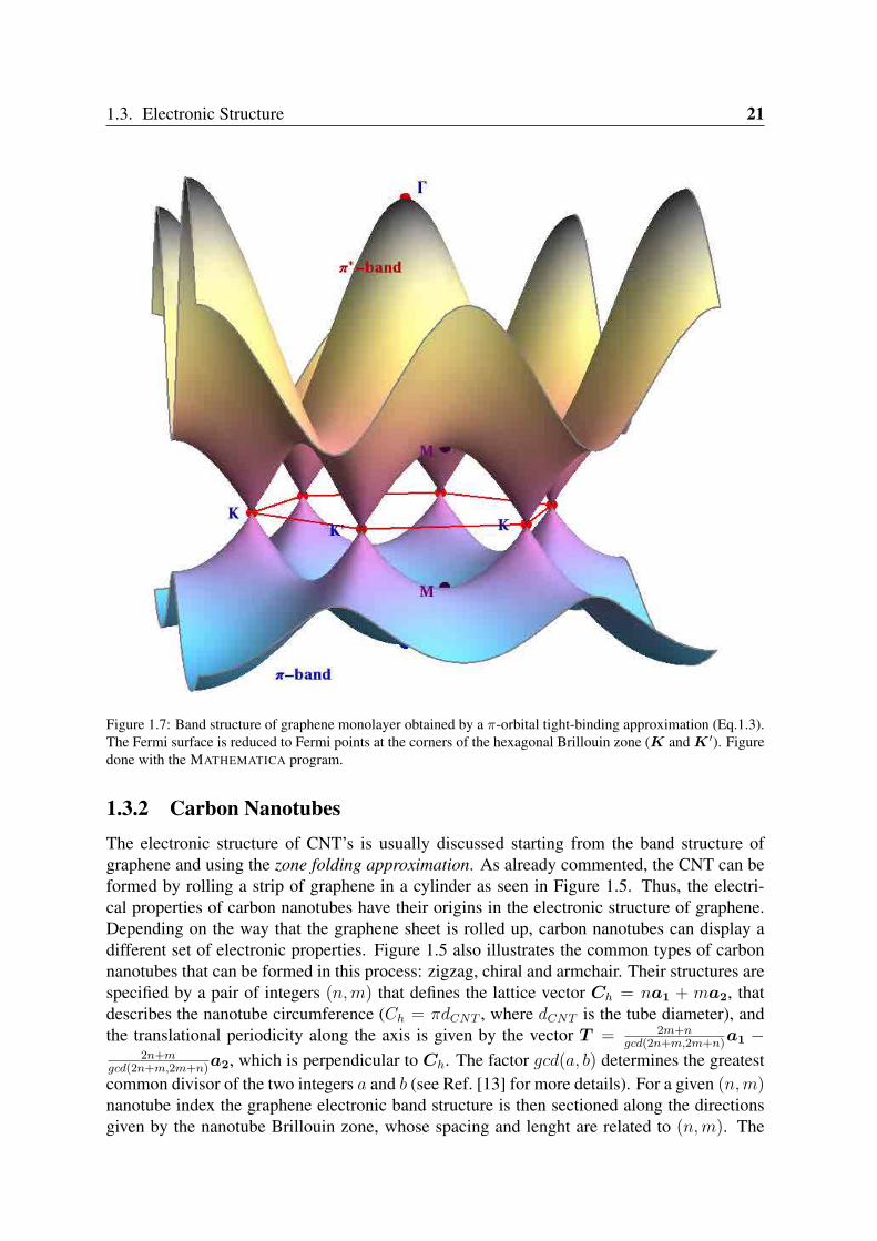
The characteristic shape of the resulting band structure E(k) is displayed in Figure 1.7. Thereare two symmetric bands coming from the eigenvalues E(k). They touch at six points, whereE(k) = 0, but only two of them are inequivalent. Henceforth they will be called Dirac pointswith momenta K and K
′ , respectively. This band structure is symmetrical with respect tothe Dirac points, and since there is one electron per atom, a neutral graphene sample will
1.3. Electronic Structure 19
Figure 1.5: The structure of graphene and carbon nanotubes. A nanotube can be formed by rolling a ribbonof graphene along a lattice vector, Ch, defined by two integers, (n,m), such as the (4,2) lattice vector showhere. Specifically, (n, n) nanotubes (armchair) are always metallic, and (n,m) nanotubes with n − m = 3j,where j = 1, 2, 3, ..., are nearly metallic. Tubes with n − m = 3j are semiconductors. Insets for nanotubes arereproduced from WikiCommons.
20 Chapter 1. Introduction
Figure 1.6: The honeycomb structure of graphene along with its first Brillouin zone in reciprocal space. Thelattice vectors a1 and a2 have an angle of 60o and a length a =
√3dC−C ∼ 2.46 Å. The reciprocal lattice vectors
bi (i = 1, 2), defined by bi · bj = 2πδij form an angle of 120o and have a length of ai = 4π/√
3dC−C ∼ 5.11Å−1.
be at half-filling (π bands), i.e. Dirac points also form the Fermi surface of neutral graphene.Corrections by considering next nearest neighbors and orbital overlaps can break this electron-hole symmetry [12]. As shown in Figure 1.7, the dispersion relation close to the Dirac pointscan be linearised. Let us take one of the Dirac points, say K, and make an expansion aroundit, k = K + q, for small q compared to K we find:
E(K + q) = E(q) ≈ ±vF h|q| (1.4)
where vF =√
3aγo/2h is called the Fermi velocity. By replacing numerical values, wefind vF ≈ 106 m/s. A similar result can be obtained for K ′, where another valley exists.This result implies that the speed of electrons in graphene is constant, despite of any k− orenergy−dependence. This behaviour is similar to that of photons. Notice that a plot of thedispersion relation, as shown in Figure 1.7, has a peculiar shape of two opposed cones whosetips touch at the Dirac point. This is the reason why the upper band and the lower band arecommonly called Dirac cones. Thus, for graphene samples whose chemical potential is placednear the neutrality point, that corresponds to the upper cone empty and the lower cone full,then its low-energy excitations have a linear dispersion relation. Moreover, this conical formmimicks the dispersion of a relativistic, massless, Dirac particles. This is by far one of themost striking property of graphene.
1.3. Electronic Structure 21
Figure 1.7: Band structure of graphene monolayer obtained by a π-orbital tight-binding approximation (Eq.1.3).The Fermi surface is reduced to Fermi points at the corners of the hexagonal Brillouin zone (K and K ′). Figuredone with the MATHEMATICA program.
1.3.2 Carbon NanotubesThe electronic structure of CNT’s is usually discussed starting from the band structure ofgraphene and using the zone folding approximation. As already commented, the CNT can beformed by rolling a strip of graphene in a cylinder as seen in Figure 1.5. Thus, the electri-cal properties of carbon nanotubes have their origins in the electronic structure of graphene.Depending on the way that the graphene sheet is rolled up, carbon nanotubes can display adifferent set of electronic properties. Figure 1.5 also illustrates the common types of carbonnanotubes that can be formed in this process: zigzag, chiral and armchair. Their structures arespecified by a pair of integers (n,m) that defines the lattice vector Ch = na1 + ma2, thatdescribes the nanotube circumference (Ch = πdCNT , where dCNT is the tube diameter), andthe translational periodicity along the axis is given by the vector T = 2m+n
gcd(2n+m,2m+n)a1 −
2n+mgcd(2n+m,2m+n)
a2, which is perpendicular to Ch. The factor gcd(a, b) determines the greatestcommon divisor of the two integers a and b (see Ref. [13] for more details). For a given (n,m)nanotube index the graphene electronic band structure is then sectioned along the directionsgiven by the nanotube Brillouin zone, whose spacing and lenght are related to (n,m). The
22 Chapter 1. Introduction
general form of the energy dispersion for any CNT is given by:
E(µ, kz) = Eg(µK1 + kzK2
|K2|) with µ = 0, · · · , N − 1 and − π
T≤ kz <
π
T(1.5)
where Eg is the graphene dispersion relation, N is the number of graphene unit cells insidethe CNT unit cell, and K1 and K2 are the basis wavevectors in CNT Brillouin zone and aredefined as follows: K1 · T = 0, K1 · Ch = 2π; and K2 · T = 2π, K2 · Ch = 0.
The zone folding approximation is based on the constraint that any electronic wave func-tion of graphene must obey the condition ψ(r + Ch) = ψ(r). In reciprocal space, this leadsto a selection criterion for allowed k vectors based on the relation Ch · k = 2πµ, where µ isan integer. This shows the periodic boundary condition of quantum confinement around thenanotube circumference, which means that only stationary states having an integer number µof wavelengths with period k = 2π/|Ch| are allowed around the circumferential perimeter.On the other hand, the linear momentum kz changes continuously along the tubes axis as aresult of the translational periodic boundary condition.
The K point at the corner of the Brillouin zone can be expressed as K = (2b1 + b2)/3leading to a simple rule that determines whether this point belongs to the set of allowed kvectors in the rolled up system:
Ch · K2π
=(na1 +ma2) · (2b1 + b2)/3
2π=
2n+m
3(1.6)
what can also be expressed as
2n+m = 3µ (1.7)n−m+ n+ 2m = 3µ
(2n+m) − (2m+ n) = n−m
which is equivalent to the condition for n −m to be an integer multiple of 3. Whenever thiscondition holds, the K point fulfills the periodic boundary conditions, so that the Fermi energy(EF ) of graphene is in the spectrum of the CNT, i.e. the CNT is metallic1. In other cases, theclosest lines of allowed k vectors miss the Fermi point by δk = 2/3dCNT . Within the linearapproximation at the K points, this results in a gap of ∆Egap = 2vF hδk = 4vF h
3dCNT. These
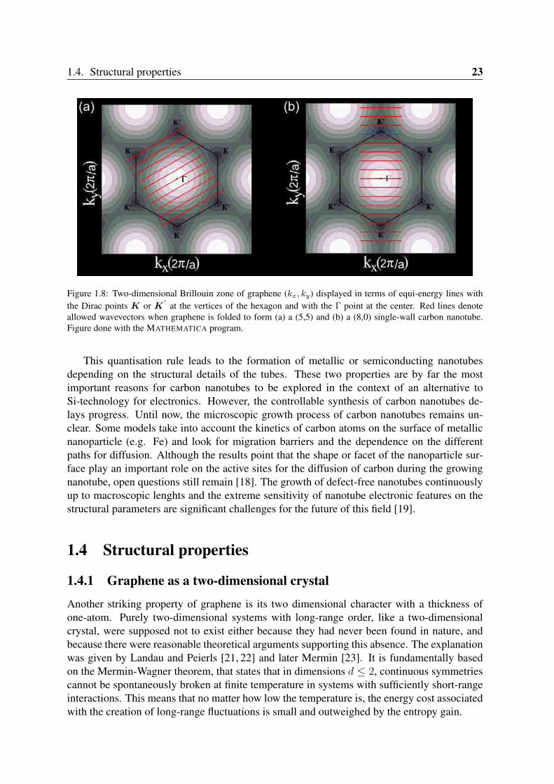
concepts can be seen straightforwardly in Figure 1.8 that shows the two-dimensional Brillouinzone of graphene but with the cutting lines superposed.
Generally, the zone-folding approximation works reasonably well for large diameter CNTsbut breaks down in thin CNTs due to curvature effects. In armchair CNTs this does not havemuch qualitative effects, because the bands crossing at the charge neutrality point are strictlyprotected by the intrinsic supersymmetry of the system [14]. In thin "metallic" zigzag andchiral CNTs, however, the calculation with more refined tight-binding parametrisation revealsa tiny gap opening at the Fermi energy [15,16], which has also been confirmed experimentally[17].
1In other words, a CNT is metallic if a cutting line passes through a Dirac point K or K′, otherwise is
semiconductor.
1.4. Structural properties 23
Figure 1.8: Two-dimensional Brillouin zone of graphene (kx, ky) displayed in terms of equi-energy lines withthe Dirac points K or K
′at the vertices of the hexagon and with the Γ point at the center. Red lines denote
allowed wavevectors when graphene is folded to form (a) a (5,5) and (b) a (8,0) single-wall carbon nanotube.Figure done with the MATHEMATICA program.
This quantisation rule leads to the formation of metallic or semiconducting nanotubesdepending on the structural details of the tubes. These two properties are by far the mostimportant reasons for carbon nanotubes to be explored in the context of an alternative toSi-technology for electronics. However, the controllable synthesis of carbon nanotubes de-lays progress. Until now, the microscopic growth process of carbon nanotubes remains un-clear. Some models take into account the kinetics of carbon atoms on the surface of metallicnanoparticle (e.g. Fe) and look for migration barriers and the dependence on the differentpaths for diffusion. Although the results point that the shape or facet of the nanoparticle sur-face play an important role on the active sites for the diffusion of carbon during the growingnanotube, open questions still remain [18]. The growth of defect-free nanotubes continuouslyup to macroscopic lenghts and the extreme sensitivity of nanotube electronic features on thestructural parameters are significant challenges for the future of this field [19].
1.4 Structural properties
1.4.1 Graphene as a two-dimensional crystal
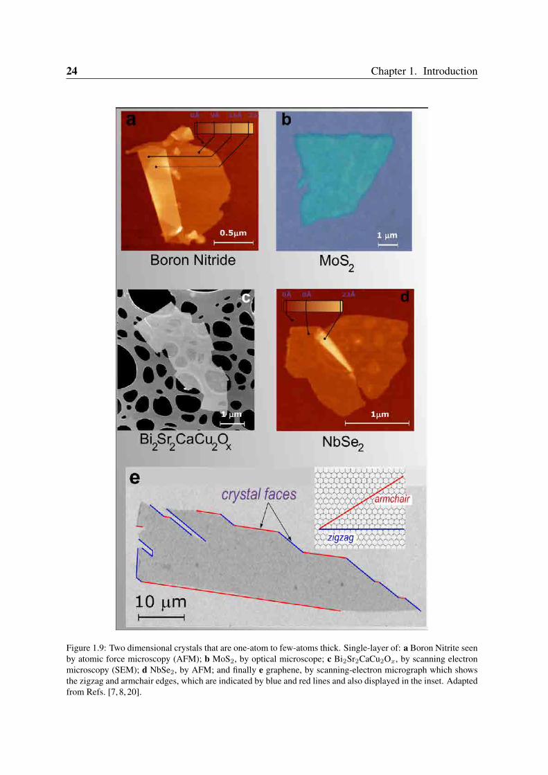
Another striking property of graphene is its two dimensional character with a thickness ofone-atom. Purely two-dimensional systems with long-range order, like a two-dimensionalcrystal, were supposed not to exist either because they had never been found in nature, andbecause there were reasonable theoretical arguments supporting this absence. The explanationwas given by Landau and Peierls [21, 22] and later Mermin [23]. It is fundamentally basedon the Mermin-Wagner theorem, that states that in dimensions d ≤ 2, continuous symmetriescannot be spontaneously broken at finite temperature in systems with sufficiently short-rangeinteractions. This means that no matter how low the temperature is, the energy cost associatedwith the creation of long-range fluctuations is small and outweighed by the entropy gain.
24 Chapter 1. Introduction
Figure 1.9: Two dimensional crystals that are one-atom to few-atoms thick. Single-layer of: a Boron Nitrite seenby atomic force microscopy (AFM); b MoS2, by optical microscope; c Bi2Sr2CaCu2Ox, by scanning electronmicroscopy (SEM); d NbSe2, by AFM; and finally e graphene, by scanning-electron micrograph which showsthe zigzag and armchair edges, which are indicated by blue and red lines and also displayed in the inset. Adaptedfrom Refs. [7, 8, 20].
1.4. Structural properties 25
There are some examples that could be used to show this feature, for instance, in the two-dimensional Ising model [24]. With a Hamiltonian given by:
H = −J∑
<i,j>
Si · Sj (1.8)
with nearest neighbour coupling J and spins Si, the average magnetization can be calculatedas < S1st >= 1 − (1/2)
∑α< σα2 >, where
∑α
< σα2(0) >=1
βJ
∫ 1/a d2k
(2π)2
1
k2(1.9)
where a is the lattice spacing, σ and α the field fluctuations, or low energy excitations. Theintegral above has a term proportional to∫ 1/a
k−1 dk (1.10)
which is logarithmically divergent. This means that low energy excitations at low temperatureslead already to deviations from the ground state. This argument explains why no thermallystable magnetic order occurs in two dimension (and even on one).
We now translate these concepts to graphene theory and formulate the problem in termsof vibrations or phonons: The thermal fluctuations of phonon modes lead to displacementsof atoms that become comparable to interatomic distances at any finite temperature. In fact,the melting temperature of thin films rapidly decreases with decreasing thickness, and theybecome unstable (separate into islands or decompose) at a thickness of, typically, dozensof atomic layers [25]. For this reason, atomic monolayers have so far been known only asan integral part of larger three-dimensional structures, usually grown epitaxially on top ofmonocrystals with matching crystal lattices.
Two dimensional materials were assumed not to exist until 2004. However, new experi-ments were able to isolate graphene [7] and other free-standing two-dimensional crystals [20],for example, single-layer boron nitride, NbSe2 and MoS2, as seen in Figure 1.9. Grapheneis a two-dimensional crystal living in a three-dimensional world, and the latter can provide amechanism to stabilize the in-plane stretching fluctuations by coupling them to out-of-planebending modes. Real samples would be crumpled, something that was experimentally con-firmed [26]. In those experiments, graphene on a scaffold geometry developes some "ripples"which have static undulations of typical sizes ∼ 5 − 10 nm and height variation ∼ 0.5 nm.
1.4.2 Ripples at free-standing grapheneHowever, the origin of the observed corrugation in graphene is still controversial, since de-pending on the particular experiment is not clear whether ripples are formed spontaneously orinduced by corrugations from the substrate, or by some chemical agent present in the environ-ment. In the case of graphene on top of SiO2, there are experimental evidences indicating thatthe corrugations come from the substrate, because a clear correlation between both of themwas observed [27,28]. However, in the case of suspended graphene spontaneous formation ofripples after heating and cooling the samples has also recently been reported [29].
26 Chapter 1. Introduction
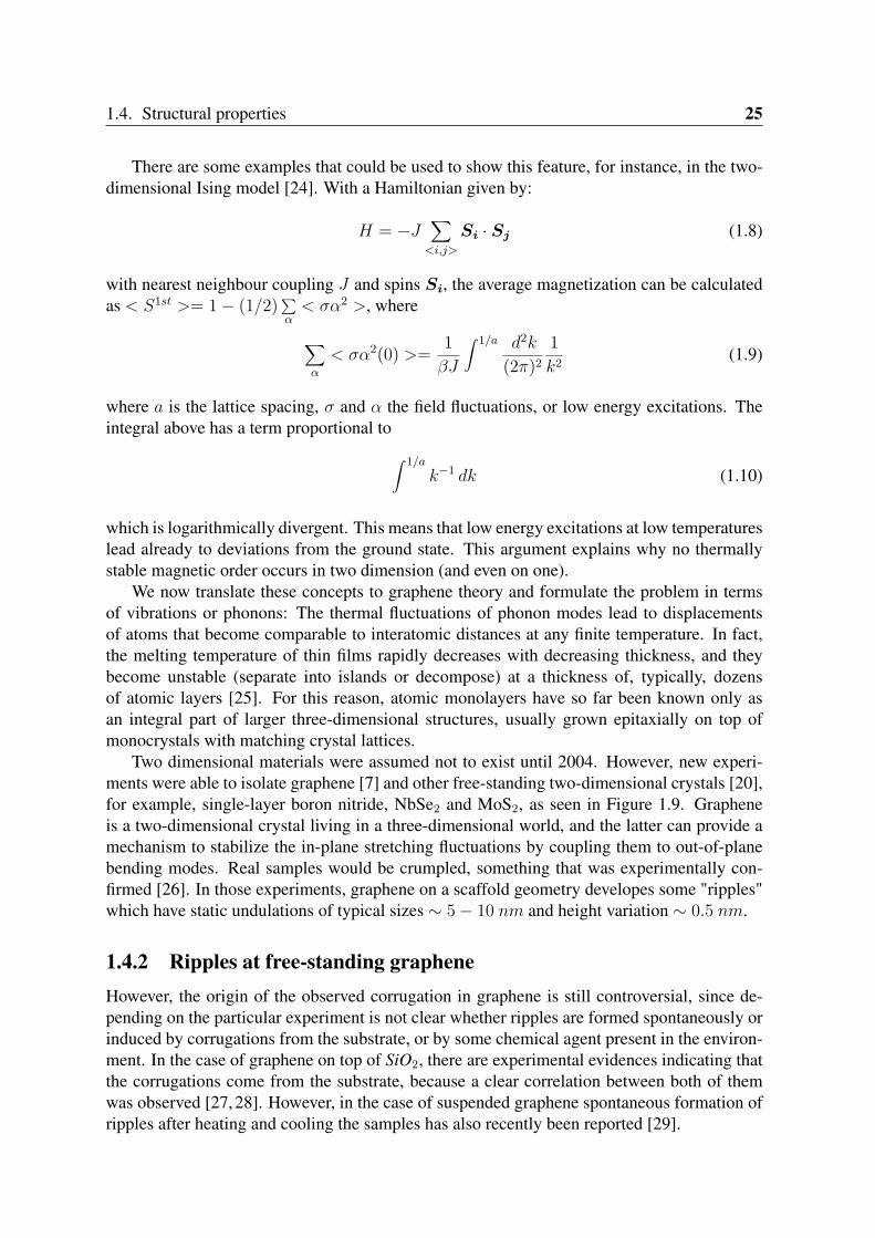
First attempts to answer why graphene crumples are given by soft-condensed matter the-ory. A continuous model of the membranes embedded in three dimensions [30] showed thatalthough mostly flat membranes exist, they are not perfectly flat, but they have intrinsic ripples.In fact, corrugations of graphene flakes have been observed [26, 31] recently by TransmissionElectron Microscopy (TEM) and diffraction techniques which somehow agree with this the-ory [30]. Those experiments are summarised in Figure 1.10. The flat graphene sheet in realspace (Fig.1.10(a)) and its 3D Fourier transform (Fig.1.10(c)) consist of a set of rods perpen-dicular to the reciprocal hexagonal lattice. For that graphene, the intensity of diffraction peakscould vary with the tilt angle, but without broadening. If the peaks become wider with increas-ing tilt angle it indicates that the rods move around their average direction (Fig. 1.10(d)-(i))and form cones indicating that the sheet is slightly corrugated (Fig. 1.10(b)). Such roughnessresults in a diffraction pattern formed for an ensemble of two-dimensional crystallites withdifferent orientations in relation to the average plane. Figure 1.10(e)-(f) show the diffractionpatterns for 0o and 14o tilt angles, respectively. The broadening of the diffraction peaks is largefor the latter pattern and it is marked by the arrows. This behaviour vanishes for an increasingnumber of layers as we can see in Figure 1.10(g). The peak broadening can also be seen inFigure 1.10(h) which illustrates the evolution of the peak width for different tilt angles. Thepeaks are sharp at normal incidence and their width increases almost linearly with tilt angle.
1.5 Magnetism in Carbon-Based Materials
The observation of magnetism in, until a few years ago, so considered non-magnetic materialsis receiving much attention, both experimental and theoretically [32]. Materials that alreadypossess attractive properties, such as low density, biocompatibility, plasticity, capacity to formdiverse structures, and that, in principle, could develop magnetic features have stimulated thefield of magnetism based in light-elements. Among all candidates, carbon-based systems arecurrently gaining special importance [33]. Carbon-based magnetic materials would greatlyextend the limits of technologies relying on the magnetism of d and f elements or dilutedmagnetic semiconductors. Room temperature metal-free magnets could find applications inmedicine, nanotechnology and telecommunications, and give the prospect for carbon-basedelectronics as already described in the previous sections. Additionally, carbon-based materialsare quite promising for spintronics and related applications due to their long spin relaxationand decoherence times owing to the low intrinsic spin-orbit interaction and the low hyperfineinteraction of the electron spins with the carbon nuclei [34–37]. Therefore, to find alternativeroutes to create pristine magnetic carbon is an important research topic and it will be thesubject of the next section.
1.5.1 Radiation-induced defect formation and ferromagnetism
Graphite in its ideal pristine form is diamagnetic. Nevertheless, several experimental groupsrecently reported the occurrence of ferromagnetic signals of different strengths in graphitesamples after proton irradiation [38, 39], chemical modification, electron bombardment, orhydrogen plasma treatment [33], even at room temperatures. The presence of magnetic metalsas dopants was experimentally excluded (or it was present only at negligible level), indicating
1.5. Magnetism in Carbon-Based Materials 27
Figure 1.10: Graphene monolayer at a (a) flat and (b) rippled geometry. (c) The reciprocal space for a flatgraphene sheet, in which the diffraction intensities form a sharp set of rods (red). (d) Similar to panel (c) butfor the corrugated graphene where the diffracted intensities are obtained by a superposition of many rods withslightly different orientation. (e),(f) Electron diffraction patterns from a graphene monolayer under incidenceangles of 0o and 14o, respectively. The tilt axis is horizontal. (g) Full widths at half maxima (FWHM) for somediffraction peak in monolayer, bilayer and graphite as a function of the tilt angle. The dashed lines are the linearfits yielding the average roughness. (h) Peak profiles reflection for different incidence angles (black line) andGaussian fits (red curve), with an offset that corresponds to the tilt angle in degrees. A cone that connects thecurves at approximately their FWHM is drawn as guide to the eye. (i) Side view of the peak broadening fordifferent diffraction beams which turns the rods into cone-shaped volume. Thus, the the diffraction spots becomeblurred at large angles what is indicated by the dotted lines. Adapted from Ref. [26, 31].
28 Chapter 1. Introduction
that magnetism should come from the graphite itself. Although the origin of magnetic orderin pure carbon is only poorly understood, some guesses have been considered.
Radiation damage of matter is governed by the displacement of atoms from their equi-librium positions due to electronic excitations and direct collisions of high-energy particleswith the nuclei. In metals and narrow band gap semiconductors electronic excitations quenchinstantaneously, leaving collisions with nuclei as the main mechanism responsible for the cre-ation of defects in graphite and related carbon materials [40]. If the kinetic energy transferredfrom a high-energy electron or ion to the nucleus is higher than the displacement thresholdTd, a carbon atom can leave its initial position to form a metastable defect structure on a sub-picosecond time scale. Such events are called knock-on displacements. For highly anisotropiclayered carbon materials the threshold of the off-plane displacement is T⊥
d ∼ 15− 20eV [41],while the creation of a defect due to the in-plane knock-on collision requires higher transferredenergies T ∥
d ≥ 30eV . Possible defects produced by radiation damage include separated andintimate pairs (Frenkel-pairs) [42, 43] of interstitial atoms and vacancies, and in-plane topo-logical defects involving non six-membered rings, e.g. Stone-Wales defect [44]. Thus, it isbelieved that the appearance of bound states due to lattice disorder is one of the main drivingforces for a decrease in the diamagnetism and an increase in the spin density in graphite [33].
Several theoretical studies have also suggested that the intrinsic magnetism is due tothe presence of undercoordinated carbon orbitals originated by impurities, boundaries or de-fects [45,46]. All these defects produce also quasilocalized states close to the EF and can giverise to a net magnetic moment. It is worth noting that these states extend over several nanome-ters around the defects and, in the case of vacancies, can form a characteristic superstructurerecognised as (
√3 ×
√3)R30o in STM images. By analysing the position and the orientation
of the superstructures, one can locate the defect and determine the sublattice to which the va-cancy belongs [47]. The fact that quasilocalized states lie at EF suggests that magnetism canbe induced by electronic exchange. It has been argued recently, that Stoner ferromagnetismwith high Curie temperatures Tc can be expected for sp electron systems [48]. Furthermore,the narrow impurity band is an essential ingredient for the ferromagnetism observed in thosesystems. However, one should take care of the inhomogeneous spatial distribution of defectsin the system in order to obtain good estimates of Tc [48].
1.6 Vacancy-induced magnetism
1.6.1 π−Vacancy
As we mentioned in the previous section, several experiments have reported the observation ofmagnetism in carbon materials. The main explanation is due to the presence of defects, suchas vacancies, cracks, or edges, that change the coordination of the carbon atoms and generatespin polarized states in the defective region, with energies close to the EF . Defects and edgesare therefore crucial to explain the magnetic properties. Based on that, the mechanism leadingto ferromagnetism in carbon structures can be understood intuitively by means of the Hubbardmodel for the honeycomb lattice which we now introduce.
Magnetism is a physical property that is directly related to electron-electron interactions.The Hubbard model [49] helps to add the effects of electron-electron interactions to systemswhose bare band structure is well described by a tight-binding model. The model assumes
1.6. Vacancy-induced magnetism 29
that the Coulomb interaction is screened, so that it can be represented by an on-site repulsionterm of strength U . The Hamiltonian for the model reads:
H = −t∑
<i,j>,σ
c†iσcjσ + U∑i,σ
ni↑ni↓ (1.11)
where< i, j > stands for nearest neighbors of the honeycomb lattice and σ for the spin degreeof freedom (↑ , ↓). The first term in Eq. (1.11) corresponds to the one-orbital per site pz tight-binding model that is obtained as the interactions are switched off. An approximate value ofthe Hubbard coupling U in graphene can be estimated in several ways from first principlescalculations. The values obtained usually lie in the range U/t ≈ 1 − 2 [50], but higher valueshave also been quoted [12]. Due the exponential growth of the Hilbert space dimension withthe number of sites N a standard way to solve the Hubbard model is by means of a mean-field theory. A direct exact diagonalization of the Hubbard model (1.11) at half-filling is onlypossible for systems until about 20 sites [51]. Thus, in order to treat problem with more thanjust few atoms Eq.1.11 is approximated by:
HMF = −t∑
<i,j>,σ
c†iσcjσ + U∑i,σ
(⟨ni↑⟩ni↓ + ni↑⟨ni↓⟩ − ⟨ni↑⟩⟨ni↓⟩) (1.12)
where i and j runs over all lattice sites and t ∼ 2.5 eV.Graphene is an example of a bipartite lattice, i.e. a lattice consisting on two different
sublattices A and B where atoms A are only linked to atoms B and vice-versa. Concerning theground state of a Hubbard model in such a lattice, Elliott Lieb [52] proved a useful theorem fora repulsive value of the Hubbard interaction U , the ground state of the half-filled lattice is non-degenerate and has a total spin equal to half the number of unbalanced atoms 2S = NA −NB.This rule has been confirmed recently in a number of studies of graphene with vacancies,edges or larger defects [53–55], and in the graphene bilayer [56]. As a result, Lieb’s theoremhas become a paradigm for magnetic studies in graphene clusters and nanographite [50]. Themajor part of these works have an imbalance between the two sublattices, NA = NB. Forinstance, a vacancy removes an atom of a given site. An additional complication beyond thescope of Lieb’s theorem has to be taken into account. When an atom is removed, two scenariosare possible. Either the disrupted bonds remain as dangling bonds or the structure undergoesa bond reconstruction with several possible outcomes (we will come to this point in the nextsections). In both cases, a local distortion of the lattice is expected.
In the following discussion, however, it is assumed that, as first approximation, the cre-ation of a vacancy has the effect of removing a pz orbital at a lattice point, together with itsconduction band electron. This is the so-called a π-vacancy2. In this sense, the physics of theconduction band electrons is still described by Eq. 1.12, where now the hopping to the vacancysites is forbidden. If the distribution of vacancies is uneven between the two sublattices, zeroenergy levels or quasilocalized states will necessarily appear at EF . In other words, wheneverthe two sublattices are not balanced with respect to their number of atoms, there will appearNA − NB states with energy E = EF and localized at the majority sublattice [12, 52]. Theground state at half-filling has either a spin up or spin down occupying the localized state at
2We have used vacancies to exemplify this rule, but it holds as well as for a hydrogen atom on top of agraphene atom as we will see in the next section.
30 Chapter 1. Introduction
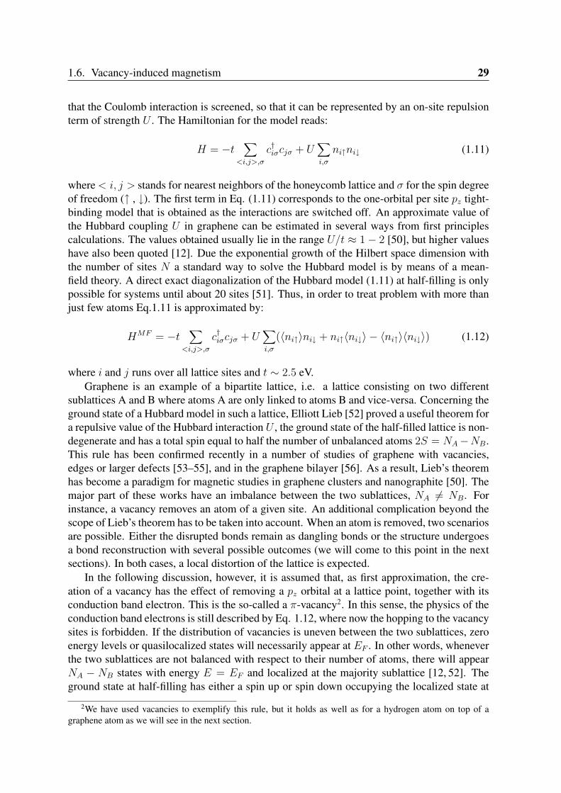
E = EF , so a net magnetic moment localizes around the vacancy for an arbitrarily small valueof the Coulomb interaction U [57]. In Figure 1.11(a) we show a typical spin density arounda vacancy in a π-tight binding model. It can be seen that short-range ferrimagnetic order isinduced around the vacancy site. The spin density on the opposite sublattice to the vacancy islarger than that on the same sublattice.
We now consider two vacancies at the same sublattice (e.g. (A,A)). In this situation, theground state is degenerate at U = 0 with four degenerate states appearing at EF as seen inFigure 1.11(b). Without the Coulomb interaction, singlet and triplet states are degenerate andLieb’s theorem guarantees that the triplet state becomes the ground state in the presence ofa Hubbard U (> 0). At finite U a local moment is induced around both vacancies and theycouple ferromagnetically. Figure 1.11(c) also shows the weak modification of the local spinmoment M local
t as a function of U for different distances lmax from the vacancy site.When two vacancies are at different sublattices (e.g. (A,B)) the problem becomes different.
Now, the eigenvalues generated by the vacancies do not vanish in general (see Figure 1.11(d)).When the distance r between them is large, the energy position of the vacancy state goes tozero [53, 55, 57]. This means that vacancies interact: a vacancy at sublattice A creates a statewith a wavefunction which is only finite on sublattice B, and vice-versa, and sites of type Aand B are connected by the electronic Hamiltonian. This results in a splitting between thetwo quasilocalized states associated with the vacancies on different sublattices and they movefrom E = EF (see inset (II) in Figure 1.11(b)). At any value of U , two of the quasilocalizedstates are now occupied and the total moment vanishes. This still agrees with the Lieb’stheorem [52], but it is possible to have a non-zero local magnetic moment at each vacancy site.Figure 1.11(e) shows the behaviour of the total sublattice magnetization M s
tot as a function ofthe distance r between two vacancies located at different sublattices. When the distance issmall between them, r/a ≤ 6, no local magnetic moment appears. However, when theyare far away from each other, a local moment is induced around each vacancy. In this case,the induced net moments at the defect sites are antiparallel. This can be understood as aconsequence of the antiferromagnetic tendency of the half-filled honeycomb lattice. In fact,the net moments induced around defects are also equal in magnitude. In Figure 1.11(c) wesee that a critical value of Ucr is needed to create a finite moment in the system. Although wehave only focus on vacancies in an infinite graphene layer, the results discussed here also holdfor ribbons [54] and other carbon geometries [50]. It is noteworthy that the quasilocalizedstates around EF have a strong directional character, as we can see in Figure 1.11(f) for twomonovacancies in an armchair graphene nanoribbon. Depending on the alignment betweenthe two vacancies, their magnetic coupling is not invariant against the exchange of positionsbecause the quasilocalized states could hybridise differently [54]. In the inset of Figure 1.11(f)the splitting energy differs when both vacancies are positioned in a tail-tail (B + A) or head-head (A+B) configuration. The physics of a π-vacancy in graphenic nanostructures is thus arich topic which will have an important place in the next parts of the present thesis. Therefore,the interpretations and arguments exposed in this section will be used below.
1.6.2 Real carbon vacancySo far, we have focused on the electronic properties of a π-vacancy in graphenic nanostruc-tures. However, the vacancy in the real word reconstructs due to the other sp electrons that arenot considered explicitly in the Hubbard Hamiltonian Eq.(1.12). The vacancy can thus display
1.6. Vacancy-induced magnetism 31
Figure 1.11: (a) Spin density around a vacancy in graphene using a pz-tight binding model. The area of thecircles is proportional to the magnitude of the spin density at each lattice point. Empty and filled circles repre-sent positive and negative magnetic moments, respectively. (b) Spin configuration at the ground state with twovacancies (I) at the same sublattice and (II) at the opposite one. In panel (I), when U = 0 four levels appearat the EF , with two levels per spin channel. At finite U (> 0), the degeneracy is split up with two states beingoccupied of spin up. In panel (II), despite of the value of U , two of the states are occupied and the total momentalways vanishes. (c) Local spin moment M local
t as a function of U for a lattice L×L. The value Ucr denotes thecritical value of U when a finite moment appears. The value lmax is the distance between the vacancy sites. (d)Energy E of a vacancy state created by two vacancies at different sublattices as a function of the distance r. (e)Total sublattice magnetization Ms
tot as a function of the distance r between two vacancies in different sublattices.The lattice constant is a = 2.46. (f) DOS for an armchair ribbon of W = 7a with two vacancies in differentorientations. The solid lines correspond to the B + A case (left lower inset) and the dashed lines correspond tothe A + B case (left upper inset). Right inset: Bonding-antibonding energy splitting as a function of the distancebetween vacancies for two different alignments. Adapted from Refs. [54, 55, 57].
32 Chapter 1. Introduction
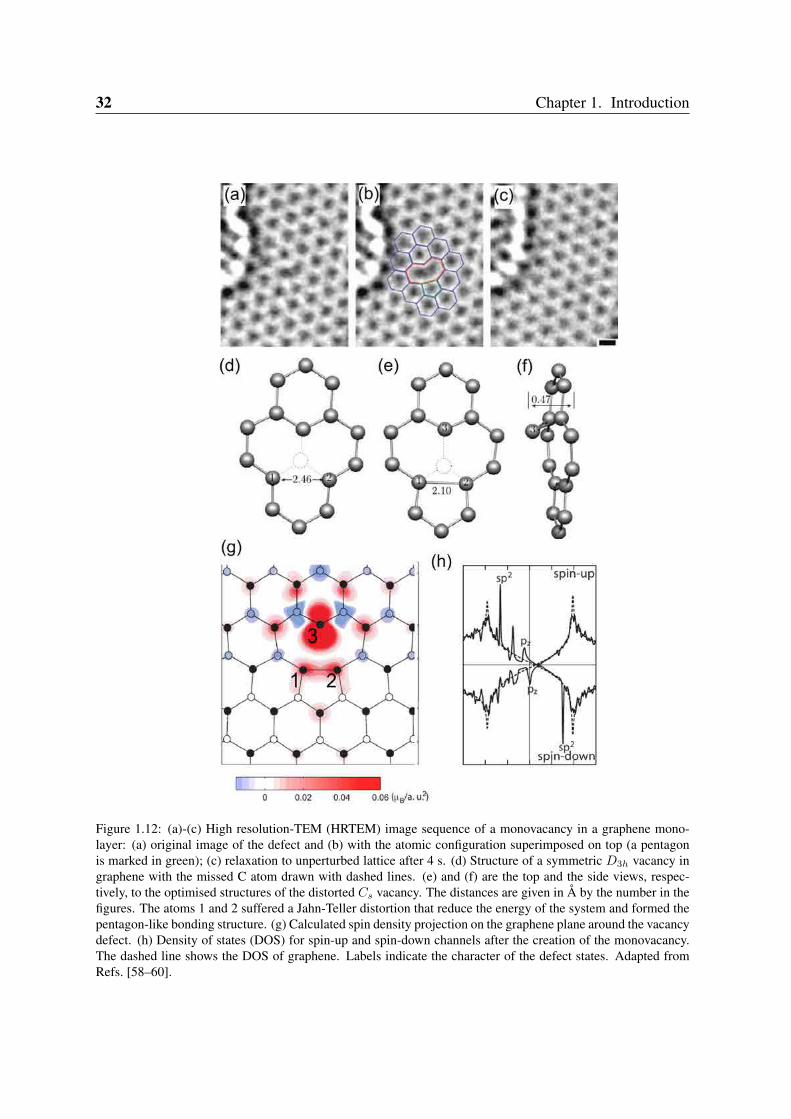
Figure 1.12: (a)-(c) High resolution-TEM (HRTEM) image sequence of a monovacancy in a graphene mono-layer: (a) original image of the defect and (b) with the atomic configuration superimposed on top (a pentagonis marked in green); (c) relaxation to unperturbed lattice after 4 s. (d) Structure of a symmetric D3h vacancy ingraphene with the missed C atom drawn with dashed lines. (e) and (f) are the top and the side views, respec-tively, to the optimised structures of the distorted Cs vacancy. The distances are given in Å by the number in thefigures. The atoms 1 and 2 suffered a Jahn-Teller distortion that reduce the energy of the system and formed thepentagon-like bonding structure. (g) Calculated spin density projection on the graphene plane around the vacancydefect. (h) Density of states (DOS) for spin-up and spin-down channels after the creation of the monovacancy.The dashed line shows the DOS of graphene. Labels indicate the character of the defect states. Adapted fromRefs. [58–60].
1.7. Impurities in graphene 33
new electronic and geometric features beyond those present in a pz tight-binding model. Inthe following, we shall address the experimental observation of a monovacancy in grapheneand also its basic electronic and magnetic properties.
For graphene, several experiments have observed vacancies and more complex defects[59, 61–63]. Those experiments irradiate the sample for some time using a focused electronbeam. Similar to proton irradiation in graphite (as seen in Section 1.5.1) but now with asubnanometer spot (e.g. ∼ 1 − 3 Å). Vacancies can be created with atomic precision atpredefined positions. For instance, we show a sequence of HRTEM images taken at roomtemperature of a reconstructed monovacancy in a single-layer graphene in Figure 1.12 (a)-(c).The vacancy is observed by the formation of a pentagon-like bond (see Figure 1.12(b)). Aftera few seconds the missing atom is replaced by a mobile adatom on the graphene surface as isseen in Figure 1.12(c). The monovacancy reconstructs in a geometry of Cs symmetry differentfrom the D3h structure displayed in Figure 1.11(a). The D3h vacancy undergoes a Jahn-Tellerdistortion. This effect is shown by first principles calculations [60] which predict an energylowering of about 0.20 eV, divided into two parts: (i) the in-plane and symmetry preservingdistortion with 0.09 eV, and (ii) the out-of-plane and symmetry lowering with 0.11 eV. Thereconstructed geometries are plotted in Figure 1.12(e)-(f). For the symmetric D3h vacancy(Figure 1.12(d)), the bond length between the first nearest neighbour atoms to the vacancy andthe next-nearest neighbours is shortened to 1.37 Å while the nearest-neighbour bond length inperfect graphene is ∼ 1.42 Å. This distortion preserves the symmetry and lowers the energyby ∼0.09 eV. Other bond lengths are only slightly changed. For the ground-state Cs, thedistortion forms a pentagon-like structure with a bond length of ∼2.1 Å.
The bond formation that accompanies the symmetry lowering lowers the energy by ∼0.10eV. Atom 3 suffers an out-of-plane displacement. This can be explained because the pairedelectrons in the new bond between atoms 1 and 2 in Figure 1.12(e) repel the electron on theopposite atom 3, so that the easiest direction for moving is an out-of-plane displacement offew tenths of an Angstrom [60]. We show the spin density projection on the graphene surfacegenerated by the reconstructed monovacancy in Figure 1.12(g). Most of the spin momentof the vacancy (∼1.04 µB) is due to atom 3, with a resulting spin pattern that only followsapproximately the original bipartite character of the graphene lattice. The bipartite characteris actually broken by the 1 − 2 bond.
Although this description of the monovacancy seems to be detailed, substantially, as wewill see in Chapter 5, this picture is still incomplete in order to fully understand the magnetismof monovacancies in graphene. There are more ingredients that determine the stability of spinsolutions in a vacancy and its interplay with the global structure can create novel effects.
1.7 Impurities in grapheneTo exploit the unique electronic properties of graphene requires to understand the effects ofimpurities in this material. Impurities are inevitable sources of electron scattering left from theproduction process and they may limit electron transport in graphene to a substantial extent.However, apart from being just undesirable, impurities provide a powerful tool for controllingthe electronic properties of graphene. In solid state materials, a clear application of impuritystates is the doping of semiconductor. In addition, impurities in graphene allow us to addressfundamental questions: for instance, impurity states in this material are directly related to
34 Chapter 1. Introduction
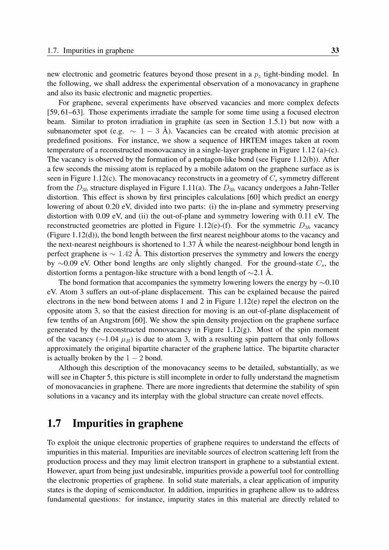
Figure 1.13: (a) Geometry of a H atom chemisorbed on top of a C atom in graphene. (b) Spin density projectionaround the H atom. (c) The resulting density of states (DOS) for spin-up and spin-down states after the doping.The dashed line shows the DOS of the ideal graphene. Labels indicate the character of the defect states. (d)Structure of the full hydrogenated graphene monolayer, graphane, in the chair conformation. The panel showsthe hexagonal carbon network with carbon in the sp3 hybridization. (e) Geometry of half-hydrogenated graphenemonolayer (graphone) that was predicted to display magnetic behaviour. (f) Band structure of graphane with aclear band gap. Adapted from Refs. [58, 64–67].
1.7. Impurities in graphene 35
Figure 1.14: (a) Schematic structure of a back-gated CNT-FET device. (b) AFM image of the device: CNTwith a backgate made by SiO2 and source (S) and drain (D) electrodes. (c) Chemical gating effects in the semi-conducting CNT. Current versus gate voltage curves before (circles) and after NO2(triangles) or NH3 (squares)exposures. The measurements with NH3 and NO2 were carried out successively after sample recovery. Adaptedfrom Refs. [72, 73].
scattering of relativistic quasiparticles [68–71]. In this section we describe how adsorbatesand impurities modify the electronic properties of graphenic nanostructures. We describe howmagnetism can be generated by using H atoms chemisorbed on graphene and we give someexamples of experiments where adsorbates can modify the electron transport. Later we shalldescribe our own investigation on the effect of substitutional metallic impurities in grapheneand CNTs, taking into account recent experimental observations.
1.7.1 H atoms chemisorbed on graphene
In the previous section we have seen how missing atoms can create a magnetic order ingraphene monolayers. Despite of being a quite different defect from a vacancy, chemisorbedmolecules and atoms on graphene, in particular H atoms, could also generate magnetism. Herewe describe the main electronic and magnetic properties caused by this kind of functionaliza-tion in order to understand the magnetism generated by more complex adsorbates in Chapter4.
36 Chapter 1. Introduction
A H atom chemisorbed on top of a C forms a σ-bond and makes the sp2 configuration tochange into an approximately sp3 configuration, as shown in Figure 1.13(a). This removes apz-orbitals from the π− π∗ band system and generates a spin density (Figure 1.13(b)), similarto that from a monovacancy in a π-tight-binding model of graphene (see Figure 1.12(g)). Ifmore than one H is adsorbed, the graphene sublattice will play a role: for adsorption at A-sublattice, the spin-density localises at B sublattice, and vice-versa3. When a H atom has beenadsorbed on the surface, an unpaired electron is left on the neighbouring C atoms, which due toits resonant character is shared with the nearest neighbours. In fact, the nearest C neighbourscontain most of the 1.0 µB magnetization. It is important to remark that there is one defectstate for each spin channel. The degeneracy is lifted when the exchange-correlation effectsare taken into account leading to separation of the graphene bands for spin-up and spin-downstates with a magnetic moment of 1.0 µB per defect and exchange splitting 0.23eV at 0.5% Hconcentration [58] (see Figure 1.13(c)).
A recently reported material that could be seen as a fully hydrogenated version of grapheneis the so-called graphane [74] which is shown in Figure 1.13(d). As graphene, pure graphaneconsists of a hexagonal lattice of carbon atoms, however, with atoms in a sp3 hybridization.In addition to the three neighboring carbon atoms, each carbon atom is covalently bonded toH atoms on alternate sides of the graphene surface. Graphane, as well as graphene, can beviewed as a crystal consisting of two surfaces without an interlayer. It is thus not surprisingthat this material is very sensitive to its environment. By attaching H atoms only to onegraphene side as shown in Figure 1.13(e) one can create a new material based on graphene.Theoretically predicted to be magnetic, this half-hydrogenated graphene or graphone [65] isseen as an alternative way to create a magnetic material based completely in light atoms. Onthe other hand, graphane presents a non-magnetic semiconducting behaviour [75] as seen inFigure 1.13(f).
In general, by adding functional groups to graphene its properties can be significantlychanged and turned to a particular application. We will have the opportunity to discuss thisfascinating problem more extensively in another chapter, being one of the topics selected forthis thesis.
1.7.2 Molecular adsorption on graphene and carbon nanotubes
Other important issue of the chemistry of graphene and CNT’s as well is the molecular ad-sorption, in addition to light atoms as H, of molecules, radicals, polymers, etc, which is alsocalled functionalization. Similar to organic chemistry in which functional groups are added toan organic molecule in order to change its properties, the same principles also hold for carbon-based materials. By attaching functional groups to the graphitic structure, both chemical andphysical features can be tailored.
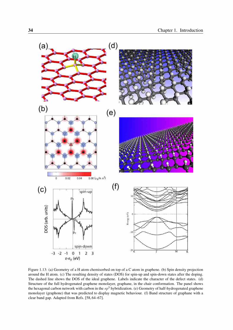
Experiments showed that adsorbates on graphene and related materials can strongly af-fect, apart from the magnetic properties, charge transport by doping and causing scattering ofelectrons. Since 2000, CNT based gas sensors have been reported [72, 73, 77]. They place asemiconducting CNT on a SiO2/Si substrate and make contacts with normal metallic elec-trodes. By using Si as a back gate, a field effect transistor (FET) is constructed as shown inFigure 1.14(a)-(b). The gate voltage Vg between tube and Si substrate is used to charge the
3The Lieb’s theorem also holds for this situation.
1.7. Impurities in graphene 37
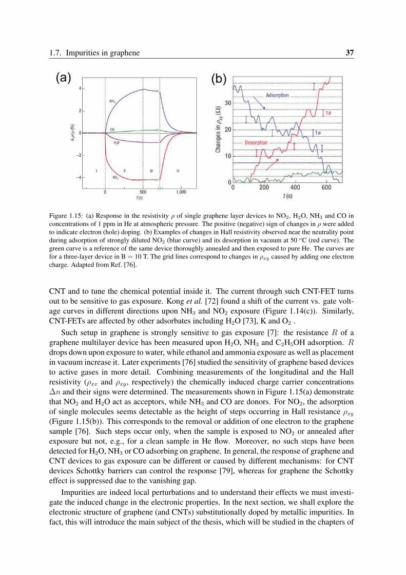
Figure 1.15: (a) Response in the resistivity ρ of single graphene layer devices to NO2, H2O, NH3 and CO inconcentrations of 1 ppm in He at atmospheric pressure. The positive (negative) sign of changes in ρ were addedto indicate electron (hole) doping. (b) Examples of changes in Hall resistivity observed near the neutrality pointduring adsorption of strongly diluted NO2 (blue curve) and its desorption in vacuum at 50 oC (red curve). Thegreen curve is a reference of the same device thoroughly annealed and then exposed to pure He. The curves arefor a three-layer device in B = 10 T. The grid lines correspond to changes in ρxy caused by adding one electroncharge. Adapted from Ref. [76].
CNT and to tune the chemical potential inside it. The current through such CNT-FET turnsout to be sensitive to gas exposure. Kong et al. [72] found a shift of the current vs. gate volt-age curves in different directions upon NH3 and NO2 exposure (Figure 1.14(c)). Similarly,CNT-FETs are affected by other adsorbates including H2O [73], K and O2 .
Such setup in graphene is strongly sensitive to gas exposure [7]: the resistance R of agraphene multilayer device has been measured upon H2O, NH3 and C2H5OH adsorption. Rdrops down upon exposure to water, while ethanol and ammonia exposure as well as placementin vacuum increase it. Later experiments [76] studied the sensitivity of graphene based devicesto active gases in more detail. Combining measurements of the longitudinal and the Hallresistivity (ρxx and ρxy, respectively) the chemically induced charge carrier concentrations∆n and their signs were determined. The measurements shown in Figure 1.15(a) demonstratethat NO2 and H2O act as acceptors, while NH3 and CO are donors. For NO2, the adsorptionof single molecules seems detectable as the height of steps occurring in Hall resistance ρxy
(Figure 1.15(b)). This corresponds to the removal or addition of one electron to the graphenesample [76]. Such steps occur only, when the sample is exposed to NO2 or annealed afterexposure but not, e.g., for a clean sample in He flow. Moreover, no such steps have beendetected for H2O, NH3 or CO adsorbing on graphene. In general, the response of graphene andCNT devices to gas exposure can be different or caused by different mechanisms: for CNTdevices Schottky barriers can control the response [79], whereas for graphene the Schottkyeffect is suppressed due to the vanishing gap.
Impurities are indeed local perturbations and to understand their effects we must investi-gate the induced change in the electronic properties. In the next section, we shall explore theelectronic structure of graphene (and CNTs) substitutionally doped by metallic impurities. Infact, this will introduce the main subject of the thesis, which will be studied in the chapters of
38 Chapter 1. Introduction
Figure 1.16: TEM image of a graphene monolayer with Pt atoms at a substitutional site. An enlarged view of thearea arrowed in the left panel is seen on right inset. Adapted from Ref. [78].
results.
1.7.3 Graphene and carbon nanotubes with substitutional transition met-als
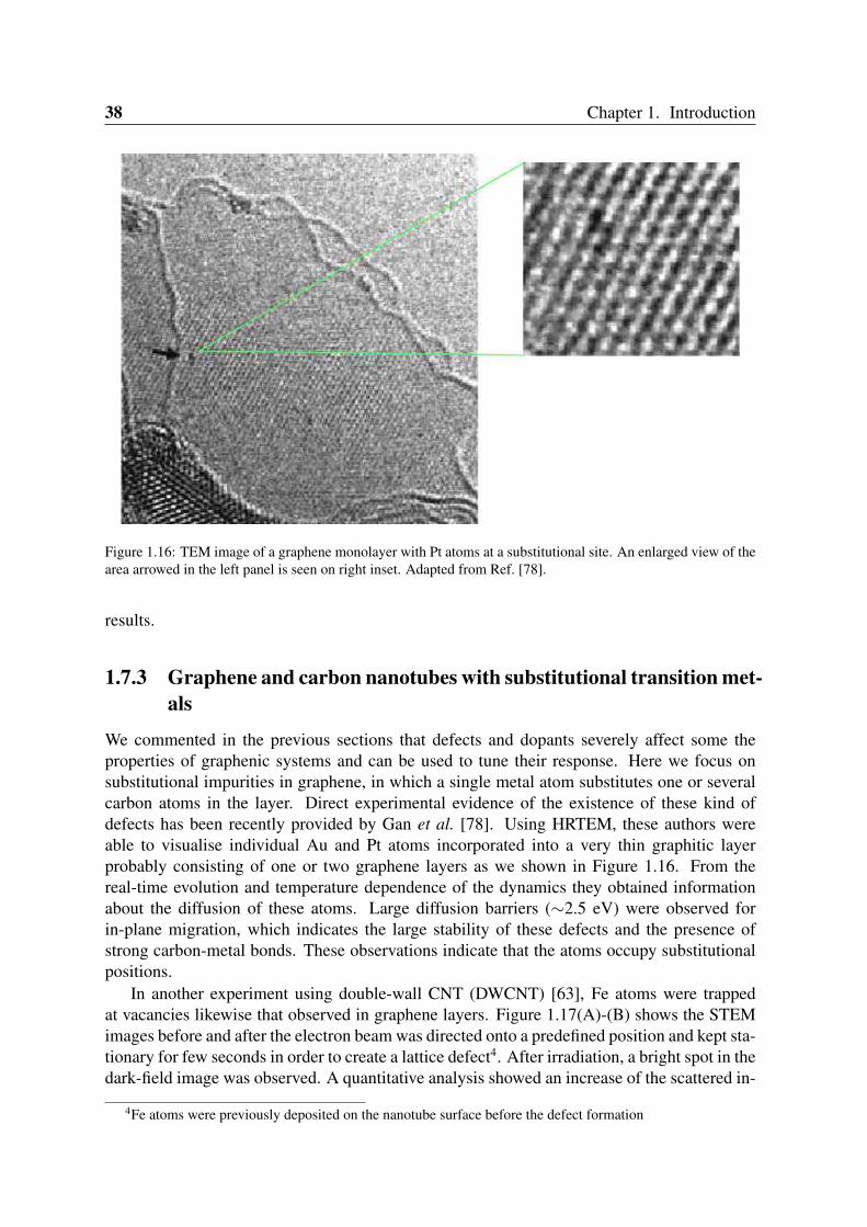
We commented in the previous sections that defects and dopants severely affect some theproperties of graphenic systems and can be used to tune their response. Here we focus onsubstitutional impurities in graphene, in which a single metal atom substitutes one or severalcarbon atoms in the layer. Direct experimental evidence of the existence of these kind ofdefects has been recently provided by Gan et al. [78]. Using HRTEM, these authors wereable to visualise individual Au and Pt atoms incorporated into a very thin graphitic layerprobably consisting of one or two graphene layers as we shown in Figure 1.16. From thereal-time evolution and temperature dependence of the dynamics they obtained informationabout the diffusion of these atoms. Large diffusion barriers (∼2.5 eV) were observed forin-plane migration, which indicates the large stability of these defects and the presence ofstrong carbon-metal bonds. These observations indicate that the atoms occupy substitutionalpositions.
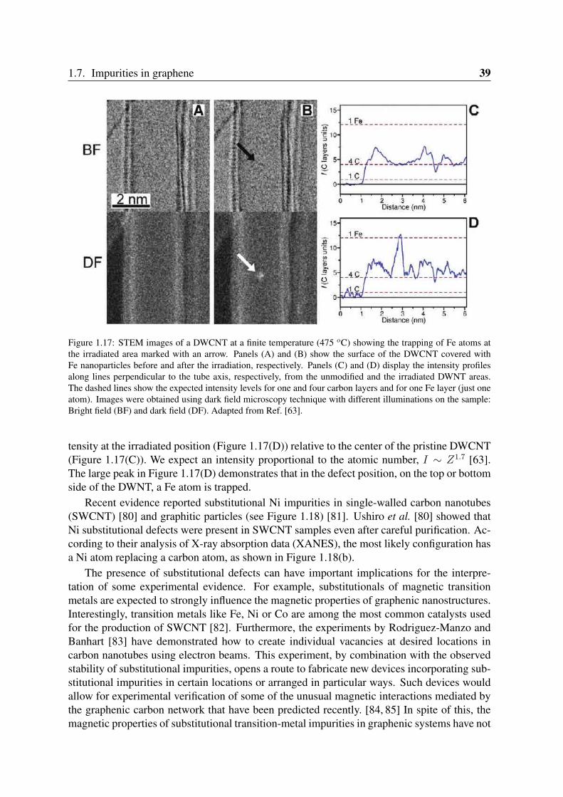
In another experiment using double-wall CNT (DWCNT) [63], Fe atoms were trappedat vacancies likewise that observed in graphene layers. Figure 1.17(A)-(B) shows the STEMimages before and after the electron beam was directed onto a predefined position and kept sta-tionary for few seconds in order to create a lattice defect4. After irradiation, a bright spot in thedark-field image was observed. A quantitative analysis showed an increase of the scattered in-
4Fe atoms were previously deposited on the nanotube surface before the defect formation
1.7. Impurities in graphene 39
Figure 1.17: STEM images of a DWCNT at a finite temperature (475 oC) showing the trapping of Fe atoms atthe irradiated area marked with an arrow. Panels (A) and (B) show the surface of the DWCNT covered withFe nanoparticles before and after the irradiation, respectively. Panels (C) and (D) display the intensity profilesalong lines perpendicular to the tube axis, respectively, from the unmodified and the irradiated DWNT areas.The dashed lines show the expected intensity levels for one and four carbon layers and for one Fe layer (just oneatom). Images were obtained using dark field microscopy technique with different illuminations on the sample:Bright field (BF) and dark field (DF). Adapted from Ref. [63].
tensity at the irradiated position (Figure 1.17(D)) relative to the center of the pristine DWCNT(Figure 1.17(C)). We expect an intensity proportional to the atomic number, I ∼ Z1.7 [63].The large peak in Figure 1.17(D) demonstrates that in the defect position, on the top or bottomside of the DWNT, a Fe atom is trapped.
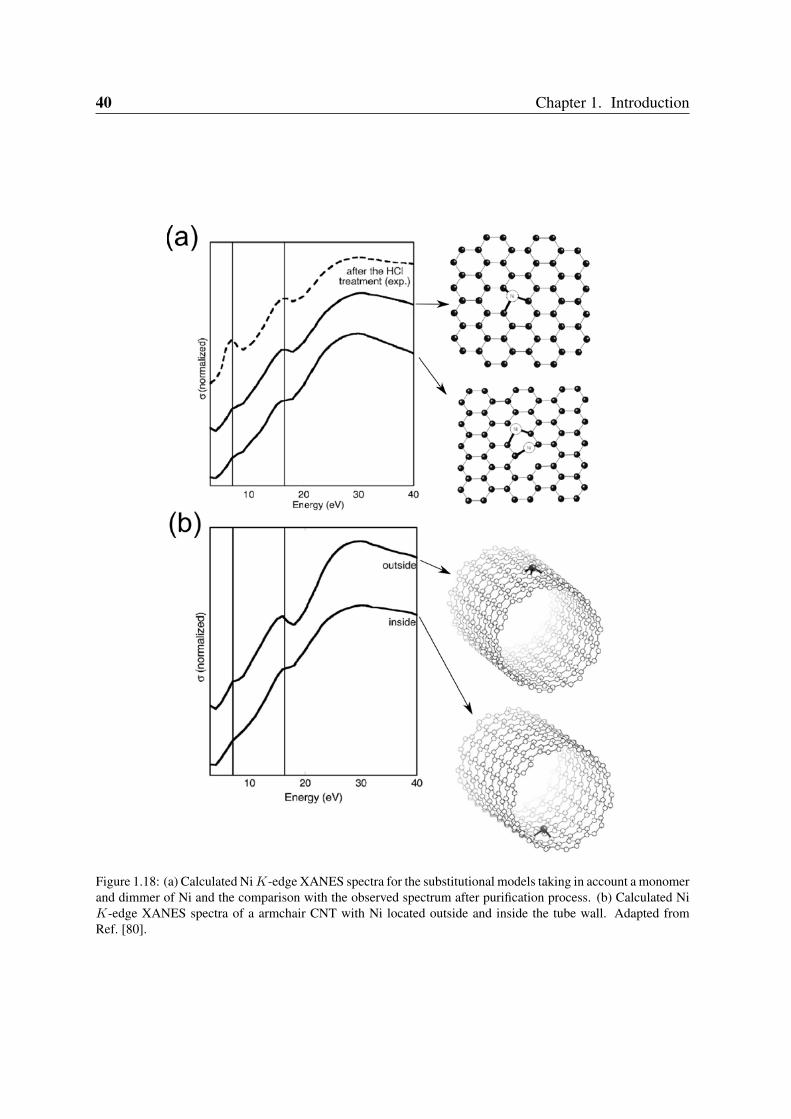
Recent evidence reported substitutional Ni impurities in single-walled carbon nanotubes(SWCNT) [80] and graphitic particles (see Figure 1.18) [81]. Ushiro et al. [80] showed thatNi substitutional defects were present in SWCNT samples even after careful purification. Ac-cording to their analysis of X-ray absorption data (XANES), the most likely configuration hasa Ni atom replacing a carbon atom, as shown in Figure 1.18(b).
The presence of substitutional defects can have important implications for the interpre-tation of some experimental evidence. For example, substitutionals of magnetic transitionmetals are expected to strongly influence the magnetic properties of graphenic nanostructures.Interestingly, transition metals like Fe, Ni or Co are among the most common catalysts usedfor the production of SWCNT [82]. Furthermore, the experiments by Rodriguez-Manzo andBanhart [83] have demonstrated how to create individual vacancies at desired locations incarbon nanotubes using electron beams. This experiment, by combination with the observedstability of substitutional impurities, opens a route to fabricate new devices incorporating sub-stitutional impurities in certain locations or arranged in particular ways. Such devices wouldallow for experimental verification of some of the unusual magnetic interactions mediated bythe graphenic carbon network that have been predicted recently. [84, 85] In spite of this, themagnetic properties of substitutional transition-metal impurities in graphenic systems have not
40 Chapter 1. Introduction
Figure 1.18: (a) Calculated Ni K-edge XANES spectra for the substitutional models taking in account a monomerand dimmer of Ni and the comparison with the observed spectrum after purification process. (b) Calculated NiK-edge XANES spectra of a armchair CNT with Ni located outside and inside the tube wall. Adapted fromRef. [80].
1.8. Thesis outline 41
been studied in detail. Few calculations have considered the effect of this kind of doping onmagnetic properties of the graphenic materials and this will be one of the main goals of thisthesis.
1.8 Thesis outlineChapter 2 address a basic introduction to the treatment of the many-body problem us-
ing Density Functional Theory (DFT). Its implementation in the SIESTA code was mainlyused through this thesis. Basic concepts on pseudopotentials, localized basis set, and periodicboundary conditions are briefly introduced. We show how some technical parameters used inthe calculations have been optimised in order to obtain a compromise between accuracy andefficiency. In particular, the convergence tests include k-points sampling, electronic smearingσ, pseudopotential radius rl and basis set. Some results for the bulk-phase of several elementsand pristine graphene are presented.
Chapter 3 deals with the structural, electronic and magnetic properties of 3d transitionmetals, noble metals and Zn atoms interacting with carbon monovacancies in graphene. Wepropose a model based on the hybridization between the states of the metal atom, particularlythe d shell, and the defect levels associated with an unreconstructed D3h carbon vacancy. Thepredictions of this model are in good agreement with the calculated DFT band structures. Withthis model, we can easily understand the non-trivial behavior found for the binding energy andfor the size and localization of the spin moment as we increase the number of valence elec-trons in the impurity.
Chapter 4 deals with the magnetism induced by metallic impurities and organic adsor-bates on graphene monolayers and SWCNTs. We have found magnetism associated withsubstitutional Co atoms and organic adsorbates (e.g. polymers, nucleobases, diazonium salts,sugar, etc) chemisorbed on graphene through a single C-C bond. Co atoms adsorbed at car-bon vacancies can be regarded as a physical realization of a simplified model of defectivegraphene: the π-vacancy. The analogy is even more direct between the π−vacancy and thecovalent functionalization. Following this analogy, the complicated magnetic properties foundin our calculations are easily understood. However, the magnetic couplings between metallicimpurities as well as between organic adsorbates on graphene are complex. These exchangeenergies are analysed in terms of a RKKY model to extract their distance dependence.
Chapter 5 focus on the interplay between elastic and magnetic properties of defects ingraphenic nanostructures. It is shown that magnetism of defects, such as in vacancies andmagnetic impurities in nanotubes and graphene, can be manipulated using strain. We findthat the magnetic moment of Ni-doped graphene can be controlled by applying tensile strain.The spin magnetic moments are greatly enhanced. Such deformation breaks the hexagonalsymmetry of the layer as in carbon nanotubes due to curvature but in a controllable way. Wealso found that monovacancies in graphene can show a very rich phase diagram of spin solu-

42 Chapter 1. Introduction
tions and geometric configurations under a biaxial strain. The moment of the monovacancyincreases with stretching while compression reduces or even kills the magnetic signal. Thetransition to a non-magnetic solution is linked to the rippling of graphene.
Finally, a summary and outlook are provided in Chapter 6.
Chapter 2
Electronic Structure Methods
A successful scheme dealing with the many-body problem is Density Functional Theory(DFT). In this Chapter, some essentials are given concerning the DFT basic theory and othertechnical concepts that we will used in this thesis, for instance pseudopotentials, k-point sam-pling, basis set, etc. A description of the main code that was used to perform all electronicstructure calculations will be also given: SIESTA. The Chapter ends with a discussion of sometests on the convergence of the physical properties (e.g. magnetic moment, band structure, ...)studied in this thesis respect to several computational parameters.
2.1 Density Functional TheoryDFT is one of the most widely used methods for electronic structure calculations in condensedmatter. Since it is an ab initio method, i.e., no fitting parameters are needed, DFT is verypowerful for the research of novel materials including nano-structured systems. With todaycomputer resources, system sizes of about a thousand atoms can be studied with many DFTmethods.
2.1.1 The many-body problemThe starting point of the description of a system containing electrons and nuclei is the Hamil-tonian:
H = − h2
2me
∑i
∇2i −∑i,I
ZIe2
|ri − RI |+
1
2
∑i=j
e2
|ri − rj|−∑I
h2
2MI
∇2I +
1
2
∑I =J
ZIZJe2
|RI − RJ |(2.1)
where lower case subscripts denote electrons, and upper case subscripts denotes nuclei. ZI
and MI are the charge and mass of the nuclei. The inverse of the nuclear masses, 1/MI , can beregarded as such small quantities that the nuclear kinetic energy can be ignored. Alternatively,one can argue that the large difference in mass between the electrons and the nuclei effectivelymeans that electrons react almost instantaneously to changes in the nuclear positions, and thenuclei can be regarded as static. This is the so-called Born-Oppenheimer approximation [86].The relevant Hamiltonian for electronic structure calculations is thus
43
44 Chapter 2. Electronic Structure Methods
H = T + Vext + Vint + EII (2.2)
where T = −12
∑i∇2
i describes the kinetic energy of electrons, Vext = −∑i,I
ZIe2
|ri−RI |is the
electron-nucleus interactions, and Vint = 12
∑i=j
e2
|ri−rj |accounts for the electron-electron in-
teractions. EII is the constant energy of the nucleus-nucleus interactions. The Hamiltonianin Eq. (2.2) is essentially determined by the external potential Vext (i.e., the nuclear coordi-nates, which also determine EII) because T and Vint are the same for any electron problem.The properties of the interacting system with N electrons are in principle obtainable from thetime-independent Schrödinger equation:
HΨi(r1, r2, ..., rn) = EiΨi(r1, r2, ..., rn) (2.3)
Solving Eq. (2.3) for a realistic system containing many electrons and nuclei is difficult formore than a few atoms. The Physics Nobel Prize winner Walter Kohn had already pointed outthat traditional wave-function methods are in general limited to molecules with a small totalnumber of chemically active electrons [87]. For N particles, the full N particle wavefunctionΨi(r1, r2, ..., rN ) has 3N variables and using a description with p parameters yields a spaceof dimension
M = p3N (2.4)
The total energy has to be minimised in the space of these M parameters. If we setup amaximum value of M , m, that can be calculated with our best computers we can have anestimation of our limits to calculate the electronic properties from wave-function methods. Asan example, if m = 109 parameters, and p = 3, for example, we can see from Eq.(2.4) that
lnm = ln(p3N) (2.5)N = 1
3ln mln p
N = 13
90.48
= 6
what means that could only treat a system of 6 particles. This is what Walter Kohn has de-scribed as the exponential wall concept and essentially it reflects the interconnectedness ofΨi(r1, r2, ..., rN ) in the 3N -dimensional configuration space defined by all rl being insidethe 3D region containing the particles [87]. Hohenberg and Kohn’s famous theorem is a (par-tial) solution to this problem and we will discuss in the following section.
2.1.2 Foundations of the Density Functional TheoryThe theoretical foundation of DFT was made by Hohenberg and Kohn [88] who showed thatthere is a one-to-one correspondence between the ground state density of a system and the
2.1. Density Functional Theory 45
external potential. In other words, two external potentials differing by more than a constantlead to two different ground state densities. Since the Hamiltonian in Eq.(2.2) is uniquelydetermined by the external potential, it follows that all properties, including excited states, ofthe system can be regarded as functionals of the ground state density. Specifically, the totalenergy can be considered as a functional of the density:
E[ρ] = T [ρ] + Vint[ρ] + Vext[ρ] = T [ρ] + Vint[ρ] +∫ρ(r)vext(r) dr (2.6)
The minimum energy is found for the ground state density ρo which can be obtained by us-ing the variational principle. Considering the three-dimensional density instead of the 3N-dimensional wavevectors as the independent variable is a worth simplification, neverthelessthe progress is still mostly formal. The problem is that the universal functionals T [ρ] andVint[ρ] of the kinetic and electron-electron interaction energies are unknown [89].
2.1.3 Kohn-Sham formulationAlmost any practical use of DFT rely on the work of Kohn and Sham (KS) from the late60’s [90]. KS theory is based on a basic ansatz, namely that the ground state density, ρ(r), ofan interacting system is also the ground state density of a non-interacting system with an effec-tive potential veff (r). The electron density is determined from a single-particle Schrödingerequation:
hψi(r) = ϵiψi(r)
(−1
2∇2 + veff (r))ψi(r) = ϵiψi(r) (2.7)
where ψi(r) are the single electron KS orbitals giving the density:
ρ(r) =∑
i
|ψi(r)|2 (2.8)
where the sum is over the occupied states. The effective potential veff (r) is given by:
veff (r) =∫ ρ(r
′)
|r − r′|dr
′+ Vext(r) +
δEXC [ρ(r)]
δρ(r)(2.9)
where the latter term is called the exchange-correlation term. The KS energy functional thatneeds to be calculated is:
E[ρ(r)] = Ts[ρ(r)] +∫Vext[ρ(r)]ρ(r) dr +
1
2
∫ ∫ ρ(r)ρ(r′)
|r − r′|dr dr
′+ Exc[ρ(r)] (2.10)
The set of equations (2.7) - (2.9) is solved self-consistently in an iterative process. For in-stance, we start by a guess of the density ρ(r), calculate veff (r), solve Eq.(2.7) to obtain
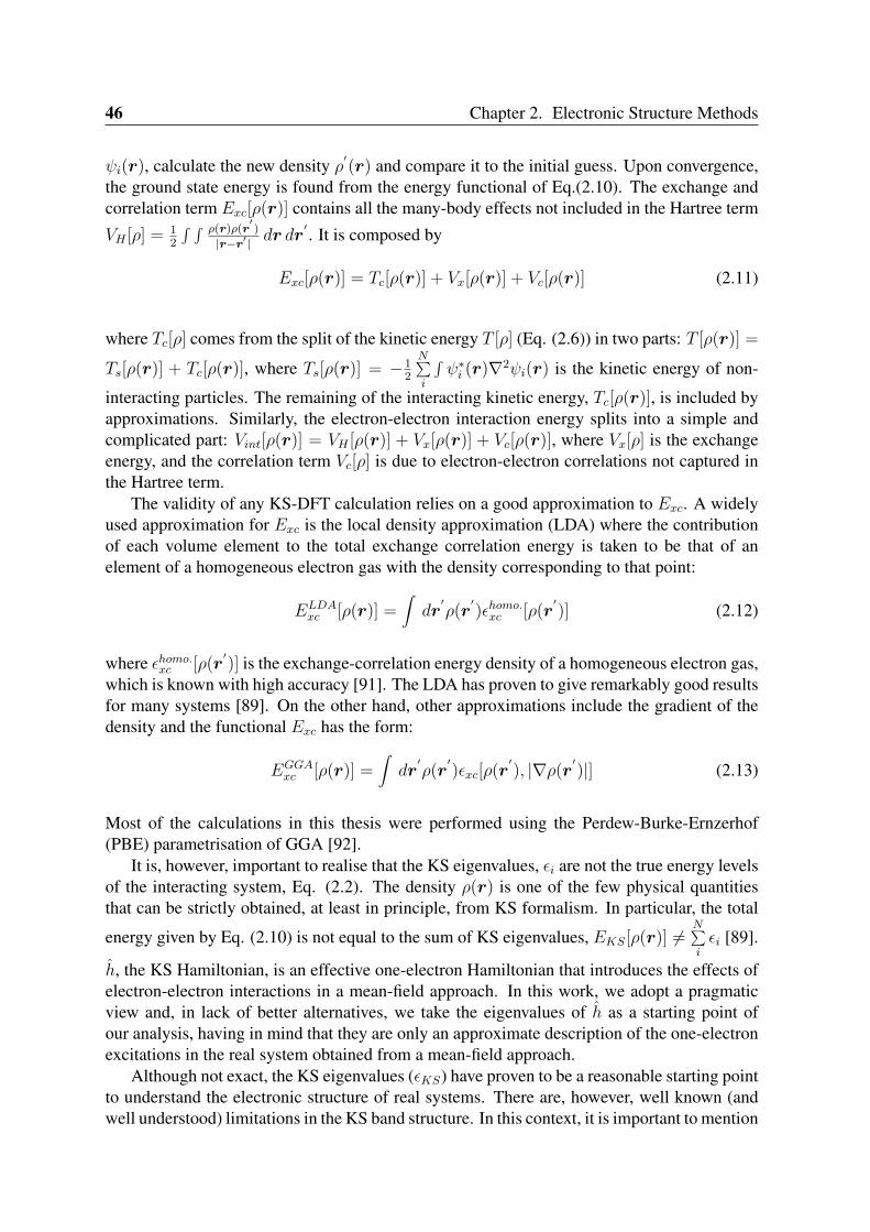
46 Chapter 2. Electronic Structure Methods
ψi(r), calculate the new density ρ′(r) and compare it to the initial guess. Upon convergence,
the ground state energy is found from the energy functional of Eq.(2.10). The exchange andcorrelation term Exc[ρ(r)] contains all the many-body effects not included in the Hartree term
VH [ρ] = 12
∫ ∫ ρ(r)ρ(r′)
|r−r′ | dr dr′ . It is composed by
Exc[ρ(r)] = Tc[ρ(r)] + Vx[ρ(r)] + Vc[ρ(r)] (2.11)
where Tc[ρ] comes from the split of the kinetic energy T [ρ] (Eq. (2.6)) in two parts: T [ρ(r)] =
Ts[ρ(r)] + Tc[ρ(r)], where Ts[ρ(r)] = −12
N∑i
∫ψ∗
i (r)∇2ψi(r) is the kinetic energy of non-
interacting particles. The remaining of the interacting kinetic energy, Tc[ρ(r)], is included byapproximations. Similarly, the electron-electron interaction energy splits into a simple andcomplicated part: Vint[ρ(r)] = VH [ρ(r)] + Vx[ρ(r)] + Vc[ρ(r)], where Vx[ρ] is the exchangeenergy, and the correlation term Vc[ρ] is due to electron-electron correlations not captured inthe Hartree term.
The validity of any KS-DFT calculation relies on a good approximation to Exc. A widelyused approximation for Exc is the local density approximation (LDA) where the contributionof each volume element to the total exchange correlation energy is taken to be that of anelement of a homogeneous electron gas with the density corresponding to that point:
ELDAxc [ρ(r)] =
∫dr
′ρ(r
′)ϵhomo.
xc [ρ(r′)] (2.12)
where ϵhomo.xc [ρ(r
′)] is the exchange-correlation energy density of a homogeneous electron gas,
which is known with high accuracy [91]. The LDA has proven to give remarkably good resultsfor many systems [89]. On the other hand, other approximations include the gradient of thedensity and the functional Exc has the form:
EGGAxc [ρ(r)] =
∫dr
′ρ(r
′)ϵxc[ρ(r
′), |∇ρ(r′
)|] (2.13)
Most of the calculations in this thesis were performed using the Perdew-Burke-Ernzerhof(PBE) parametrisation of GGA [92].
It is, however, important to realise that the KS eigenvalues, ϵi are not the true energy levelsof the interacting system, Eq. (2.2). The density ρ(r) is one of the few physical quantitiesthat can be strictly obtained, at least in principle, from KS formalism. In particular, the total
energy given by Eq. (2.10) is not equal to the sum of KS eigenvalues, EKS[ρ(r)] =N∑iϵi [89].
h, the KS Hamiltonian, is an effective one-electron Hamiltonian that introduces the effects ofelectron-electron interactions in a mean-field approach. In this work, we adopt a pragmaticview and, in lack of better alternatives, we take the eigenvalues of h as a starting point ofour analysis, having in mind that they are only an approximate description of the one-electronexcitations in the real system obtained from a mean-field approach.
Although not exact, the KS eigenvalues (ϵKS) have proven to be a reasonable starting pointto understand the electronic structure of real systems. There are, however, well known (andwell understood) limitations in the KS band structure. In this context, it is important to mention
2.2. The SIESTA method 47
that the fundamental band gap (Eg) of a semiconductor or insulator is only approximatelypredicted using the LDA or GGA exchange-correlation functionals. One of the reasons for thatin the KS approach the gap, EKS , is defined as the difference between the lowest unoccupied(ϵlumo
KS ) and highest occupied (ϵhomoKS ) eigenvalues which differs from the definition of the gap
Eg. The latter is defined as Eg = I −A, where I is the ionisation potential and A the electronaffinity. The relation between Eg and EKS is given by Eg = EKS + δxc, where δxc is thederivative discontinuity, i.e., a finite kink that the exchange-correlation potential exhibits as theparticle number crosses the integer number of particles N in the system [93]. In some casesδxc can be small but numerical investigations show that it is usually not negligible [94–96].Therefore, this can limit the prediction of the fundamental gap Eg from the eigenvalues ϵKS
even if the exact energy functional would be known.
2.2 The SIESTA method
Here we briefly mention some important aspects of the SIESTA method that were used in thisthesis. This code was chosen due to its widespread use and efficiency. A detailed descriptionof the SIESTA code can be found in Ref. [97]. SIESTA is an ab initio pseudopotential methodwhich employs a linear combination of atomic orbitals as a basis set. Due to the use of atomicorbitals as a basis set, it seems to be similar to a tight binding technique [98] but in fact itstrongly differs: the single-particle Hamiltonian is obtained by projecting the KS-DFT Hamil-tonian (Eq. 2.10) onto this basis set of atomic orbitals; thus, it is not a set of fitting parameterslike in empirical tight-binding methods. Many approximations necessary to solve the one-particle Hamiltonian in SIESTA as for instance the pseudopotential approach, the treatment ofexchange and correlation explicitly by means of approximate functionals (e.g. LDA, GGA)and the already cited Born-Oppenheimer approximation are also commom to other ab initiomethods. Apart from that, the method is also characterised by a set of parameter that controlsthe accuracy of the self-consistent KS solution. Just to cite some of them: the size (number ofatomic basis orbitals) and range (radius of the basis orbitals) of the basis set, the fineness ofreal-space integration grid, the non-linear core correction to treat exchange-correlation inter-action between core and valence states, etc.
2.2.1 Periodic boundary condition
In order to solve the KS differential equations one needs to specify the boundary conditions(BCs) for the problem. In the SIESTA method one uses periodic BCs within the supercellapproach [89]. This is the natural choice for bulk crystals, which in reality are periodic. Thesupercell approach can also be applied to non-periodic structures if a sufficient amount of vac-uum is included in the supercell, to effectively separate the objects. In this way molecules,wires, and surfaces can be studied by including vacuum in three, two, or one directions, re-spectively.
Since the supercell is periodic, Bloch’s theorem applies and the wavefunctions can bewritten as
ψnk(r) = unk(r)eik·r (2.14)
48 Chapter 2. Electronic Structure Methods
Figure 2.1: Sketch of the all-electron and pseudo potentials and their corresponding wave functions. The radiusat which all-electron and pseudo potentials match is displayed as rc. Adapted from [99].
where unk(r) has the periodicity of the supercell, k is a wave vector in the first Brillouinzone (BZ), and n is the band index. Equation (2.14) allows mapping the KS equations to thereciprocal space, where they are solved for each different k and the size of the problem isrestricted to the number of orbitals in the supercell. The expectation value of some operator,Â, is found as
⟨A⟩ =1
VBZ
∫BZ
A(k) dk ≈∑k
ωkA(k) (2.15)
where the integral is approximated by a sum over a number of k-points with weight, ωk. Ifthe supercell is large, the corresponding BZ is small, and few k-points are needed. In thenon-periodic directions only the Γ-point (ki = 0) is usually included.
SIESTA uses fast Fourier transform (FFT) to compute the Hartree potential. The FFT algo-rithm computes the discrete Fourier transform and its inverse which is in principle a periodicfunction. This allows to solve Poisson’s equation and find VH in an easy way.
2.2. The SIESTA method 49
2.2.2 Pseudopotentials
In many DFT implementations, the external potential Vext(r) is replaced by pseudopotentials(PPs). The idea is that the core electrons which are tightly bound to the nucleus are chemicallyinert and can be ignored. This leaves only the valence electrons to be considered. PPs aretypically generated for free atoms, but can be applied to solids and molecules since the corestates almost remain the same (see Figure 2.1). In SIESTA one typically uses norm-conservingPPs of the Troullier-Martins type [100].
It is also worth noting that all the interactions between the core and valence electrons mustbe transferred to the pseudopotential. This separation core-valence implies a linearisation ofthe interaction which is an approximation for the exchange-correlation energies. Note thatthe exchange-correlation energies are explicitly non-linear. If the valence ρval and core ρc(r)charge densities are well separated, as is often the case, this will introduce no serious errors.However, if there is a significant overlap between both densities, this approximation will leadto systematic errors in the total energy and reduces the transferability of the pseudopotential.In particular, this is the case for many magnetic systems, like transition metals, and theyneed the explicit consideration of the non-linear dependence of the energy on the core chargedensity. To overcome this difficulty, it was proposed that the full core charge density ρc(r)could be replaced by a partial core charge density which is identical to the true charge densityoutside some radius rc [101]. This procedure apparently simple has improved the descriptionof materials in which the overlap between core and valence charge densities is large, e.g. manymagnetic materials [89].
2.2.3 Basis set
In the numerical solution to the KS equations one expands the wave functions in terms of abasis set:
ψn(r) =∑m
cnmϕm(r) (2.16)
This is exact, if the basis set ϕm is complete. Otherwise, the expansion is an approximation.In SIESTA the basis orbitals are localized functions centered on the atoms. At an atomicposition RI , the set of orbitals are
ϕI,lmn(r) = ϕln(|rI |)Ylm(rI) (2.17)
where rI = (r) − RI , ϕln is a radial function, and Ylm are the real spherical harmonics withangular momentum labeled by l, m. For each value of l one can have multiple radial functionslabeled by n. A single-ζ (SZ) basis set have n = 1, double-ζ have n = 1, 2, etc. In the caseof carbon, the minimal basis set (SZ), consists of a single s−orbital (l = 0, m = 0) and threep−orbitals (l = 1, m = 1, 0, 1), corresponding to the four valence electrons. This basis canbe expanded by five polarization d−orbitals (l = 2, m = 2,−1, 0,+1,+2), and is denotedsingle-zeta-polarized (SZP). If n = 2 the basis is denoted double-zeta-polarized (DZP) whichis generally considered as the standard basis set in SIESTA. The radial functions have a finite
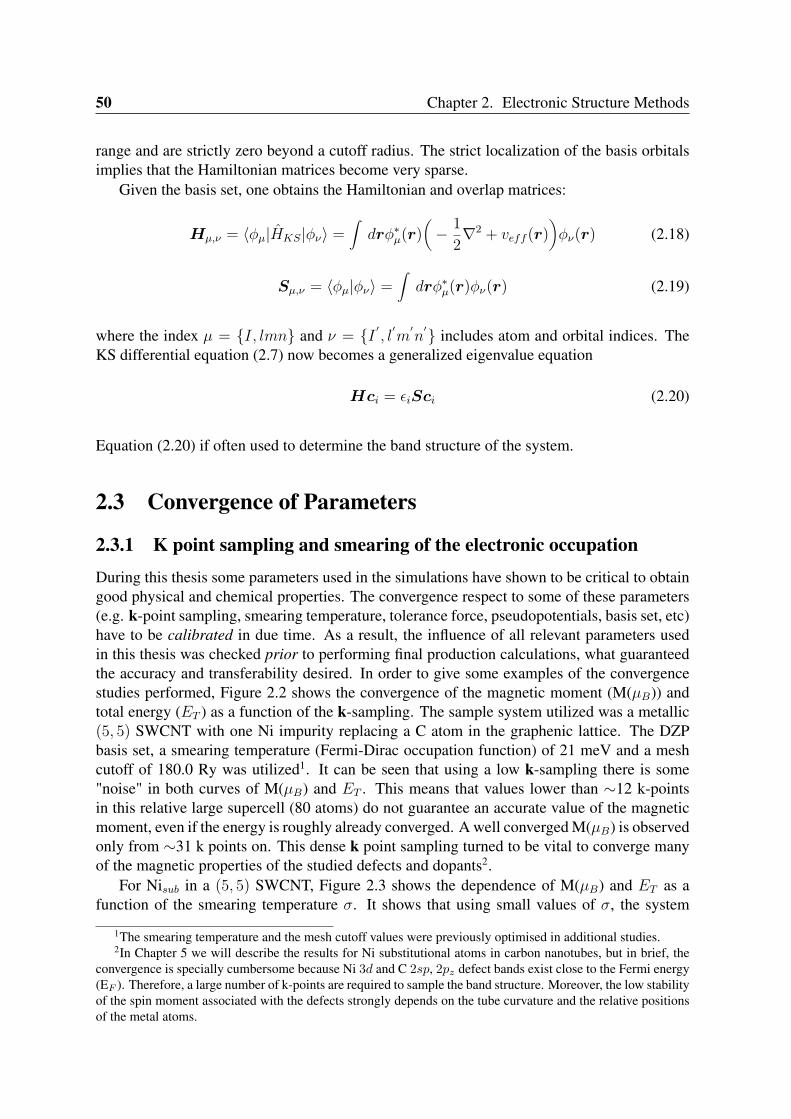
50 Chapter 2. Electronic Structure Methods
range and are strictly zero beyond a cutoff radius. The strict localization of the basis orbitalsimplies that the Hamiltonian matrices become very sparse.
Given the basis set, one obtains the Hamiltonian and overlap matrices:
Hµ,ν = ⟨ϕµ|HKS|ϕν⟩ =∫drϕ∗
µ(r)(− 1
2∇2 + veff (r)
)ϕν(r) (2.18)
Sµ,ν = ⟨ϕµ|ϕν⟩ =∫drϕ∗
µ(r)ϕν(r) (2.19)
where the index µ = I, lmn and ν = I ′, l
′m
′n
′ includes atom and orbital indices. TheKS differential equation (2.7) now becomes a generalized eigenvalue equation
Hci = ϵiSci (2.20)
Equation (2.20) if often used to determine the band structure of the system.
2.3 Convergence of Parameters
2.3.1 K point sampling and smearing of the electronic occupation
During this thesis some parameters used in the simulations have shown to be critical to obtaingood physical and chemical properties. The convergence respect to some of these parameters(e.g. k-point sampling, smearing temperature, tolerance force, pseudopotentials, basis set, etc)have to be calibrated in due time. As a result, the influence of all relevant parameters usedin this thesis was checked prior to performing final production calculations, what guaranteedthe accuracy and transferability desired. In order to give some examples of the convergencestudies performed, Figure 2.2 shows the convergence of the magnetic moment (M(µB)) andtotal energy (ET ) as a function of the k-sampling. The sample system utilized was a metallic(5, 5) SWCNT with one Ni impurity replacing a C atom in the graphenic lattice. The DZPbasis set, a smearing temperature (Fermi-Dirac occupation function) of 21 meV and a meshcutoff of 180.0 Ry was utilized1. It can be seen that using a low k-sampling there is some"noise" in both curves of M(µB) and ET . This means that values lower than ∼12 k-pointsin this relative large supercell (80 atoms) do not guarantee an accurate value of the magneticmoment, even if the energy is roughly already converged. A well converged M(µB) is observedonly from ∼31 k points on. This dense k point sampling turned to be vital to converge manyof the magnetic properties of the studied defects and dopants2.
For Nisub in a (5, 5) SWCNT, Figure 2.3 shows the dependence of M(µB) and ET as afunction of the smearing temperature σ. It shows that using small values of σ, the system
1The smearing temperature and the mesh cutoff values were previously optimised in additional studies.2In Chapter 5 we will describe the results for Ni substitutional atoms in carbon nanotubes, but in brief, the
convergence is specially cumbersome because Ni 3d and C 2sp, 2pz defect bands exist close to the Fermi energy(EF ). Therefore, a large number of k-points are required to sample the band structure. Moreover, the low stabilityof the spin moment associated with the defects strongly depends on the tube curvature and the relative positionsof the metal atoms.
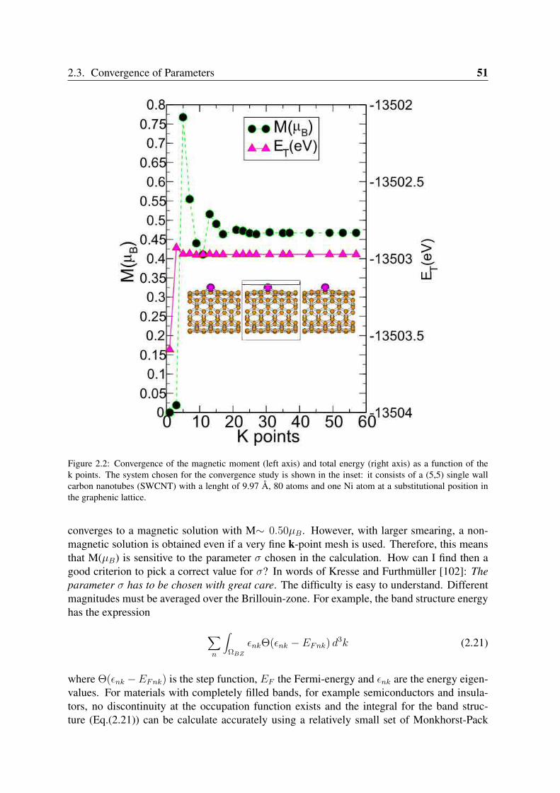
2.3. Convergence of Parameters 51
Figure 2.2: Convergence of the magnetic moment (left axis) and total energy (right axis) as a function of thek points. The system chosen for the convergence study is shown in the inset: it consists of a (5,5) single wallcarbon nanotubes (SWCNT) with a lenght of 9.97 Å, 80 atoms and one Ni atom at a substitutional position inthe graphenic lattice.
converges to a magnetic solution with M∼ 0.50µB. However, with larger smearing, a non-magnetic solution is obtained even if a very fine k-point mesh is used. Therefore, this meansthat M(µB) is sensitive to the parameter σ chosen in the calculation. How can I find then agood criterion to pick a correct value for σ? In words of Kresse and Furthmüller [102]: Theparameter σ has to be chosen with great care. The difficulty is easy to understand. Differentmagnitudes must be averaged over the Brillouin-zone. For example, the band structure energyhas the expression
∑n
∫ΩBZ
ϵnkΘ(ϵnk − EFnk) d3k (2.21)
where Θ(ϵnk −EFnk) is the step function, EF the Fermi-energy and ϵnk are the energy eigen-values. For materials with completely filled bands, for example semiconductors and insula-tors, no discontinuity at the occupation function exists and the integral for the band struc-ture (Eq.(2.21)) can be calculate accurately using a relatively small set of Monkhorst-Pack
52 Chapter 2. Electronic Structure Methods
0
0.1
0.2
0.3
0.4
0.5
M(µ
Β)
0 20 40 60 80 100 120 σ (meV)
-13503
-13502.96
-13502.92
-13502.88
-13502.84
-13502.8
ET (
eV)
Figure 2.3: Convergence of the magnetic moment (upper panel) and total energy (bottom panel) as a function ofthe smearing temperature σ. The system chosen was the same as in Figure 2.2 and a k-point sampling consistingof 1x1x31 k-points was utilized. Other parameters (basis set, mesh cutoff, etc) were fixed as in the previousconvergence study. The dashed line markes the point in which σ was assumed to converge both magnetic momentand total energy.
k-points3. However, in the case of metals, this integral converges very slowly with the numberof k-points because the occupancy change abruptly between 0 and 1 at the EF . The con-vergence in principle can be improved by using other type of function, insteat of Θ(ϵnk −EF ), with a smoother behaviour, for instance the Fermi-Dirac functional f( ϵnk−EFnk
σ) =
1exp((ϵnk−EFnk)/σ)+1
. Where σ = kBT and might be "interpreted" as a finite-temperature.Strictly speaking σ does not correspond to a temperature in the ab initio calculations but afinite broadening of the energy states in order to evaluate the integral in Eq.(2.21) more easily.This is a technical parameter that can play an important role in the convergence of magneticcalculations. In fact, a well chosen σ can be used as a tool to reduce the necessary k-samplingto calculate the electronic structure of metallic systems. In this case, an good choice of σ canbe obtained only by comparing results for different k-point meshes and different values of σwhich for this thesis was done.
2.3.2 Pseudopotentials and basis orbital radiiThe pseudopotentials used in this thesis were constructed using the Troullier-Martins receipt[100]. For this goal a set of pseudization radii rl for each relevant angular momentum channel
3The Monkhorst-Pack k-points correspond to a special set of k points equally spaced in the Brillouin zone[103]
2.3. Convergence of Parameters 53
Table 2.1: Cutoff radii (in Bohrs) used for the generation of the Troullier-Martins [100] norm-conserving pseu-dopotentials used in the SIESTA calculations. rl stands for the cut-off radius used for the l channel, while rcore isthe matching radius used for the construction of pseudocores in order to include non-linear core corrections forexchange and correlation [101].
Valence rs (ao) rp (ao) rd (ao) rcore
Sc [Ar]4s13d2 3.30 3.30 1.44 0.89Ti [Ar]4s13d3 2.96 2.96 1.45 0.72V [Ar]4s13d4 2.40 2.79 1.46 0.69Cr [Ar]4s13d5 2.51 2.80 1.46 0.65Mn [Ar]4s13d6 2.51 2.77 1.45 0.60Fe [Ar]4s13d7 2.10 2.10 1.68 0.67Co [Ar]4s23d7 2.37 2.48 1.68 0.67Ni [Ar]4s23d8 1.85 1.95 1.45 0.53Cu [Ar]4s13d10 2.33 2.30 1.79 0.53Ag [Kr]5s14d10 2.45 2.58 2.00 0.83Au [Xe,4f 14]6s15d10 2.55 2.68 2.20 0.93Zn [Ar]4s23d10 2.04 2.21 1.66 0.49Li [He]2s1 2.25 2.10 2.05 –Be [He]2s2 2.10 1.80 1.75 –B [He]2s22p1 1.40 1.40 1.75 –C [He]2s22p2 1.25 1.25 1.25 –N [He]2s22p3 1.25 1.25 1.25 –O [He]2s22p4 1.14 1.14 1.14 –F [He]2s22p5 1.19 1.19 1.19 –Al [Ne]3s23p1 1.89 1.89 1.89 –Si [Ne]3s23p2 1.89 1.89 1.89 –P [Ne]3s23p3 1.85 1.85 1.85 1.65S [Ne]3s23p4 1.60 1.85 1.75 1.45Cl [Ne]3s23p5 1.40 1.65 1.75 1.25Ge [Ar]4s24p2 1.90 2.20 3.00 1.65Sn [Kr]5s25p2 1.90 2.20 3.15 1.90Pb [Xe]6s26p2 1.98 2.80 3.51 1.50H 1s1 1.25 1.25 – –
Table 2.2: Cutoff radii (in Bohrs) of the numerical atomic orbitals (NAOs) used in SIESTA as a basis set. Theradii used for the s and polarization p shell are equal.
rNAOsp (ao) rNAO
d (ao)Co 8.00 4.73Ni 10.94 6.81Cu 8.87 5.52Ag 10.48 6.52Au 8.63 6.08Zn 9.24 5.33
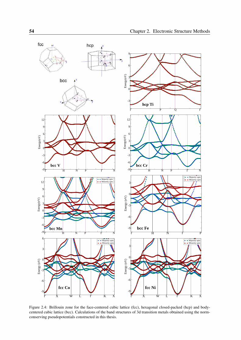
54 Chapter 2. Electronic Structure Methods
-3
0
3
6
9
Ene
rgy(
eV)
Γ ΓP Q
hcp Ti
-9
-6
-3
0
3
6
9
12
Ene
rgy(
eV)
Γ ΓH N NP
bcc V-9
-6
-3
0
3
6
9
12
Ene
rgy(
eV)
Γ ΓH N NP
bcc Cr
-9
-6
-3
0
3
6
9
12
Ene
rgy(
eV)
Majority spinMinority spin
Γ ΓH N NP
bcc Mn -9
-6
-3
0
3
Ene
rgy
(eV
)
Majority spinMinority spin
Γ H N Γ Pbcc Fe
-9
-6
-3
0
3
6
Ene
rgy
(eV
)
Majority spinMinority spin
Γ X W L X
fcc Co
Γ K
-9
-6
-3
0
3
Ene
rgy
(eV
)
Majority spinMinority spin
Γ X W L X
fcc Ni
Γ K
Figure 2.4: Brillouin zone for the face-centered cubic lattice (fcc), hexagonal closed-packed (hcp) and body-centered cubic lattice (bcc). Calculations of the band structures of 3d transition metals obtained using the norm-conserving pseudopotentials constructed in this thesis.
2.3. Convergence of Parameters 55
have to be used. Table 2.1 summarises all the information related to rl. The pseudopotentialsfor the metal atoms also include nonlinear core corrections [101] in which the pseudocoreradii (rcore) have been optimised for each element.
For most elements, the shape and radii of the basis sets of numerical atomic orbitals(NAOs) used with SIESTA were determined automatically by the code using an energy shiftparameter of 50 meV. [97,104] However, for some transition metal atoms the binding energieswhere slightly overestimated using these basis sets, mainly due to the confinement of the freeatom. For those atoms we enlarged the radii of the basis orbitals (using smaller values of theenergy shift parameter) until the binding energies were converged within a few tens of meV.Here, the reference calculations were those using plane-waves and projector-augmented wavepotentials (PAW) as implemented in the VASP code [105, 106]. The largest radius for eachelement and l channel is shown in Table 2.2. Notice that the double-ζ polarized (DZP) basisof these transition metals include a p shell. In this case the radii of the p orbitals is taken equalto that of the s shell.
2.3.3 Benchmark systems: transition metals in bulk phases and grapheneIn order to give some benchmarks of our calculation procedure, we present here the bandstructures of some transition metal atoms in bulk phases and graphene. Figure 2.4 shows theresults for Ti, V, Cr, Mn, Fe, Co, Ni in body-centered cubic (bcc), hexagonal close-packed(hcp) and face-centered cubic crystals (fcc). The majority and minority spin bands are dis-played in green and red curves, respectively, and EF is set to zero. These band structuresare in quite good agreement with previously published results using different methodologiesand also recover, taking into account the limitations of GGA calculations, the main trendsobserved in photoemission experiments.
In these type of calculations, apart from k-sampling, basis set, smearing, mesh cutoff, etc,commented above, one of the major factors that should be considered with care is the func-tional utilized. In many cases a very accurate description of magnetic materials goes beyondDFT. Early calculations of elemental ferromagnets (Fe, Co, Ni) demonstrated that GGA israther successful in the prediction of the magnetic moments when compared with Local SpinDensity Approximation (LSDA). GGA calculations lead to reliable lattice constants and spinmoments as we can see in Table 2.3, in which a comparison between calculations perfomedusing LSDA/GGA and some experiments is also presented. We can see the very favourablecomparison of our calculations using SIESTA and pseudopotentials with experiments and pre-vious calculations using all-electron methods.
Figure 2.5 shows the band structure of graphene calculated with the pseudopotential of Cpresented in Table 2.1. The unit cell consists of two atoms at a distance of 1.44 Å, and a com-parison between DZ (green curves) and DZP (black curves) basis set is also presented. Thetwo curves agree quite well for states around the Fermi level and occupied states4. However,some deviation is observed for states higher that ∼7 eV above EF which is due to the lower
4DZ basis set was observed to describe quite well, in comparison with the more complete basis set (DZP),many of the structural and electronic properties of systems in which carbon is the only element present (e.g.vacancies in graphene monolayers). Therefore, one of strategies used in this thesis was to perform the struc-tural relaxations with a smaller DZ basis, while the final results for the electronic and magnetic properties wereobtained using a more expensive DZP basis. This becomes instrumental to treat systems with more than ∼200atoms in the supercell.
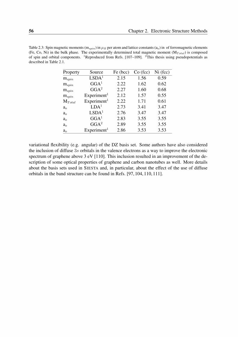
56 Chapter 2. Electronic Structure Methods
Table 2.3: Spin magnetic moments (mspin) in µB per atom and lattice constants (ao) in of ferromagnetic elements(Fe, Co, Ni) in the bulk phase. The experimentally determined total magnetic moment (MTotal) is composedof spin and orbital components. 1Reproduced from Refs. [107–109]. 2This thesis using pseudopotentials asdescribed in Table 2.1.
Property Source Fe (bcc) Co (fcc) Ni (fcc)mspin LSDA1 2.15 1.56 0.59mspin GGA1 2.22 1.62 0.62mspin GGA2 2.27 1.60 0.68mspin Experiment1 2.12 1.57 0.55MTotal Experiment1 2.22 1.71 0.61ao LDA1 2.73 3.41 3.47ao LSDA1 2.76 3.47 3.47ao GGA1 2.83 3.55 3.55ao GGA2 2.89 3.55 3.55ao Experiment1 2.86 3.53 3.53
variational flexibility (e.g. angular) of the DZ basis set. Some authors have also consideredthe inclusion of diffuse 3s orbitals in the valence electrons as a way to improve the electronicspectrum of graphene above 3 eV [110]. This inclusion resulted in an improvement of the de-scription of some optical properties of graphene and carbon nanotubes as well. More detailsabout the basis sets used in SIESTA and, in particular, about the effect of the use of diffuseorbitals in the band structure can be found in Refs. [97, 104, 110, 111].
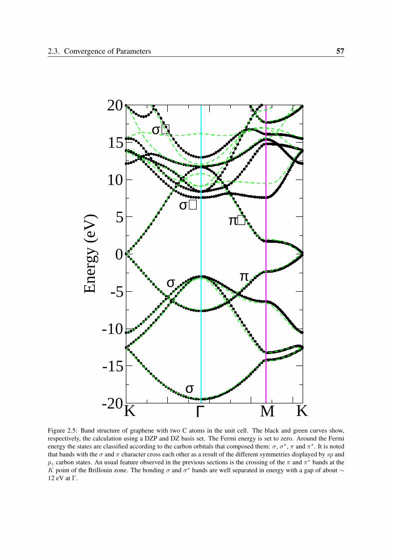
2.3. Convergence of Parameters 57
-20
-15
-10
-5
0
5
10
15
20E
nerg
y (e
V)
K Γ M K
π
π∗
σ
σ∗
σ
σ∗
Figure 2.5: Band structure of graphene with two C atoms in the unit cell. The black and green curves show,respectively, the calculation using a DZP and DZ basis set. The Fermi energy is set to zero. Around the Fermienergy the states are classified according to the carbon orbitals that composed them: σ, σ∗, π and π∗. It is notedthat bands with the σ and π character cross each other as a result of the different symmetries displayed by sp andpz carbon states. An usual feature observed in the previous sections is the crossing of the π and π∗ bands at theK point of the Brillouin zone. The bonding σ and σ∗ bands are well separated in energy with a gap of about ∼12 eV at Γ.

58 Chapter 2. Electronic Structure Methods
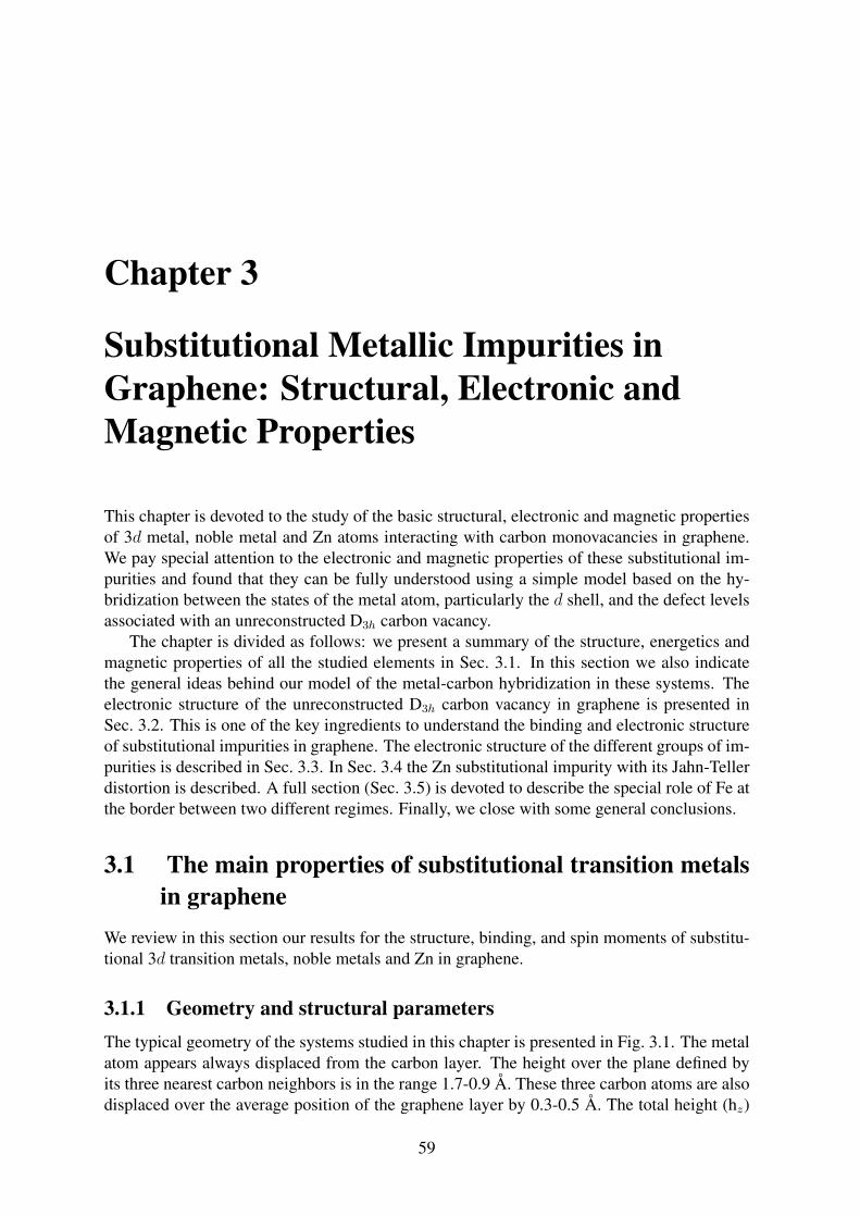
Chapter 3
Substitutional Metallic Impurities inGraphene: Structural, Electronic andMagnetic Properties
This chapter is devoted to the study of the basic structural, electronic and magnetic propertiesof 3d metal, noble metal and Zn atoms interacting with carbon monovacancies in graphene.We pay special attention to the electronic and magnetic properties of these substitutional im-purities and found that they can be fully understood using a simple model based on the hy-bridization between the states of the metal atom, particularly the d shell, and the defect levelsassociated with an unreconstructed D3h carbon vacancy.
The chapter is divided as follows: we present a summary of the structure, energetics andmagnetic properties of all the studied elements in Sec. 3.1. In this section we also indicatethe general ideas behind our model of the metal-carbon hybridization in these systems. Theelectronic structure of the unreconstructed D3h carbon vacancy in graphene is presented inSec. 3.2. This is one of the key ingredients to understand the binding and electronic structureof substitutional impurities in graphene. The electronic structure of the different groups of im-purities is described in Sec. 3.3. In Sec. 3.4 the Zn substitutional impurity with its Jahn-Tellerdistortion is described. A full section (Sec. 3.5) is devoted to describe the special role of Fe atthe border between two different regimes. Finally, we close with some general conclusions.
3.1 The main properties of substitutional transition metalsin graphene
We review in this section our results for the structure, binding, and spin moments of substitu-tional 3d transition metals, noble metals and Zn in graphene.
3.1.1 Geometry and structural parametersThe typical geometry of the systems studied in this chapter is presented in Fig. 3.1. The metalatom appears always displaced from the carbon layer. The height over the plane defined byits three nearest carbon neighbors is in the range 1.7-0.9 Å. These three carbon atoms are alsodisplaced over the average position of the graphene layer by 0.3-0.5 Å. The total height (hz)
59
60Chapter 3. Substitutional Metallic Impurities in Graphene: Structural, Electronic and
Magnetic Properties
yx
z
hz
Figure 3.1: Typical geometry of transition and noble substitutional metal atoms in graphene. The metal atommoves upwards from the layer and occupies, in most cases, an almost perfectly symmetric three-fold positionwith C3v symmetry.
of the metal atom over the graphene plane is the sum of these two contributions and rangesbetween 1.2-1.8 Å, as shown in panel (c) of Fig. 3.2. In most cases the metal atom occupies analmost perfect symmetric configuration with C3v symmetry. Exceptions are the noble metals,that are slightly displaced from the central position, and Zn that suffers a Jahn-Teller distortionin its most stable configuration. However, we have found that it is also possible to stabilize asymmetric configuration for Zn with a binding energy only ∼150 meV smaller. This configu-ration was overlooked in a recently published study on these systems [112] and we will referto it as ZnC3v throughout the chapter.
Figures 3.2 presents a summary of the structural parameters of substitutional 3d transitionmetals, noble metals and Zn in graphene. Solid circles correspond to calculations using theSIESTA code with pseudopotentials and a basis set of atomic orbitals, while open squares standfor VASP calculations using plane-waves and PAW potentials. The agreement between bothsets of calculations is quite remarkable. Data in these figures correspond to calculations usinga 4×4 supercell of graphene. For several metals we have also performed calculations usinga larger 8×8 supercell and find almost identical results. This is particularly true for the totalspin moments, which are less dependent on the size of the supercell, but require a sufficientlydense k-point sampling to converge. In the following we will mainly discuss the results ob-tained with the smaller cell since the plots of the band structures are easier to interpret in that
3.1. The main properties of substitutional transition metals in graphene 61
case. Finally, as already mentioned, noble metals and Zn present a distorted configuration.A detailed description of the structural parameters in these cases will be given below, herewe only present the averaged structural data for noble metals and those corresponding to theZnC3v case.
The data in Fig. 3.2 are basically consistent with those reported by Krasheninnikov et al. inRef. [112]. The behavior of the metal-carbon bond length and the height (hz) of the impurityover the layer reflects approximately the size of the metal atom. For transition metals thesedistances decrease as we increase the atomic number, with a small discontinuity when goingfrom Mn to Fe. The carbon-metal bond length reaches its minimum for Fe (dC−Fe=1.76 Å),keeping a very similar value for Co and Ni. For Cu and Zn the distances increase reflectingthe fully occupied 3d shell and the large size of the 4s orbitals. Among the noble metalswe find that, as expected, the bond length largely increases for Ag with respect to Cu, butslightly decreases when going from Ag to Au. The latter behavior can be understood from thecompression of the 6s shell due to scalar relativistic effects.
3.1.2 Binding energiesThe binding energies of the studied substitutional metal atoms in graphene can be found inpanel (d) of Fig. 3.2. In general, the behavior of the binding energies can be correlated withthat of the carbon-metal bond length, although the former is somewhat more complicated.Binding energies for transition metals are in the range of 8-6 eV. Ti presents the maximumbinding energy, which can be easily understood since for this element all the metal-carbonbonding states (see Sec. 3.3.1) become fully occupied. One could expect a continuous decreaseof the binding energy as we move away from Ti along the transition metal series and first thenon-bonding 3d, and later the metal-carbon antibonding levels become populated. However,the behavior is non-monotonic and the smaller binding energies among the 3d transition metalsare found for Cr and Mn, while a local maximum is observed for Co. This complex behavioris related to the simultaneous energy down-shift and compression of the 3d shell of the metalas we increase the atomic number. This will become more transparent when discussing indetail the metal-carbon hybridization levels. In brief, the behavior of the binding energies ofthe substitutional 3d transition metal comes from two competing effects:
(i) as the 3d shell becomes occupied and moves to lower energies the hybridization withthe carbon vacancy states near the Fermi energy (EF ) is reduced, which decreases the bindingenergy;
(ii) the transition from Mn to late transition metals is accompanied by a shift of the metal-carbon bond length of ∼0.1 Å, which increases the carbon-metal interaction and, correspond-ingly, the binding energy.
Binding energies for noble metals are considerably smaller than for transition metals andmirror the reverse behavior of the bond lengths: 3.69, 1.76 and 2.07 eV, respectively, for Cu,Ag and Au. The smallest binding energy (∼1 eV) among the metals studied here is found forZn, with filled s-d electronic shells.
3.1.3 Spin momentsThe spin moments of substitutional transition and noble metals in graphene are shown inFig. 3.3. Again they are in agreement with the results of Ref. [112]. However, we advance a
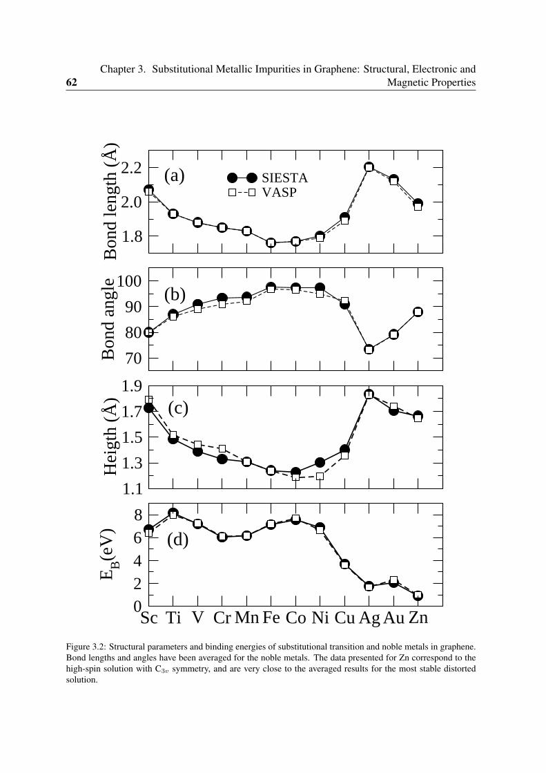
62Chapter 3. Substitutional Metallic Impurities in Graphene: Structural, Electronic and
Magnetic Properties
1.1
1.3
1.5
1.7
1.9
Hei
gth
(Å)
Sc Ti V CrMn FeCo Ni Cu Ag AuZn02468
EB(e
V)
70
80
90
100
Bon
d an
gle
1.8
2.0
2.2
Bon
d le
ngth
(Å
)
SIESTAVASP
(a)
(b)
(c)
(d)
Figure 3.2: Structural parameters and binding energies of substitutional transition and noble metals in graphene.Bond lengths and angles have been averaged for the noble metals. The data presented for Zn correspond to thehigh-spin solution with C3v symmetry, and are very close to the averaged results for the most stable distortedsolution.
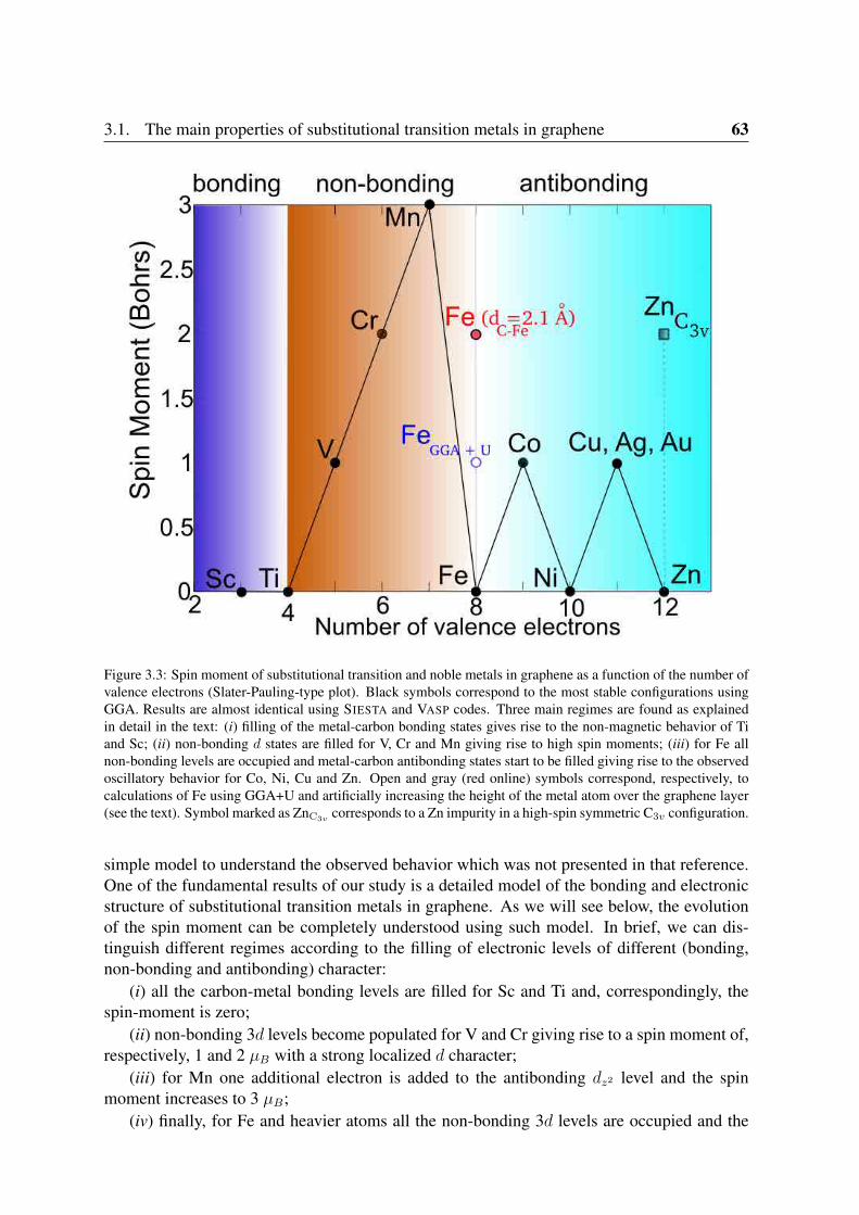
3.1. The main properties of substitutional transition metals in graphene 63
Figure 3.3: Spin moment of substitutional transition and noble metals in graphene as a function of the number ofvalence electrons (Slater-Pauling-type plot). Black symbols correspond to the most stable configurations usingGGA. Results are almost identical using SIESTA and VASP codes. Three main regimes are found as explainedin detail in the text: (i) filling of the metal-carbon bonding states gives rise to the non-magnetic behavior of Tiand Sc; (ii) non-bonding d states are filled for V, Cr and Mn giving rise to high spin moments; (iii) for Fe allnon-bonding levels are occupied and metal-carbon antibonding states start to be filled giving rise to the observedoscillatory behavior for Co, Ni, Cu and Zn. Open and gray (red online) symbols correspond, respectively, tocalculations of Fe using GGA+U and artificially increasing the height of the metal atom over the graphene layer(see the text). Symbol marked as ZnC3v corresponds to a Zn impurity in a high-spin symmetric C3v configuration.
simple model to understand the observed behavior which was not presented in that reference.One of the fundamental results of our study is a detailed model of the bonding and electronicstructure of substitutional transition metals in graphene. As we will see below, the evolutionof the spin moment can be completely understood using such model. In brief, we can dis-tinguish different regimes according to the filling of electronic levels of different (bonding,non-bonding and antibonding) character:
(i) all the carbon-metal bonding levels are filled for Sc and Ti and, correspondingly, thespin-moment is zero;
(ii) non-bonding 3d levels become populated for V and Cr giving rise to a spin moment of,respectively, 1 and 2 µB with a strong localized d character;
(iii) for Mn one additional electron is added to the antibonding dz2 level and the spinmoment increases to 3 µB;
(iv) finally, for Fe and heavier atoms all the non-bonding 3d levels are occupied and the
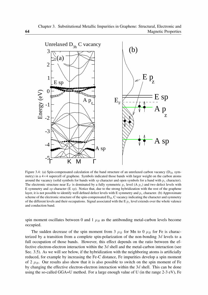
64Chapter 3. Substitutional Metallic Impurities in Graphene: Structural, Electronic and
Magnetic Properties
Γ Κ Μ Γ-5
-4
-3
-2
-1
0
1
2
3
Ene
rgy
(eV
)Unrelaxed D
3h C vacancy
A sp
A pz
E sp
(a)
E sp
A p
E pz
z
(b)
A sp
EF
Figure 3.4: (a) Spin-compensated calculation of the band structure of an unrelaxed carbon vacancy (D3h sym-metry) in a 4×4 supercell of graphene. Symbols indicated those bands with larger weight on the carbon atomsaround the vacancy (solid symbols for bands with sp character and open symbols for a band with pz character).The electronic structure near EF is dominated by a fully symmetric pz level (A pz) and two defect levels withE symmetry and sp character (E sp). Notice that, due to the strong hybridization with the rest of the graphenelayer, it is not possible to identify well defined defect levels with E symmetry and pz character. (b) Approximatescheme of the electronic structure of the spin-compensated D3h C vacancy indicating the character and symmetryof the different levels and their occupations. Signal associated with the E pz level extends over the whole valenceand conduction band.
spin moment oscillates between 0 and 1 µB as the antibonding metal-carbon levels becomeoccupied.
The sudden decrease of the spin moment from 3 µB for Mn to 0 µB for Fe is charac-terized by a transition from a complete spin-polarization of the non-bonding 3d levels to afull occupation of those bands. However, this effect depends on the ratio between the ef-fective electron-electron interaction within the 3d shell and the metal-carbon interaction (seeSec. 3.5). As we will see below, if the hybridization with the neighboring atoms is artificiallyreduced, for example by increasing the Fe-C distance, Fe impurities develop a spin momentof 2 µB. Our results also show that it is also possible to switch on the spin moment of Feby changing the effective electron-electron interaction within the 3d shell. This can be doneusing the so-called GGA+U method. For a large enough value of U (in the range 2-3 eV), Fe
3.2. Unreconstructed D3h carbon vacancy 65
impurities develop a spin moment of 1 µB. This will be also explained in detail in Sec. 3.5.For the time being we just point out that this behavior is unique to Fe: using similar values ofU for other impurities does not modify their spin moments.
At the level of the GGA calculations Fe constitutes the border between two different char-acters of the spin moment associated with the substitutional metal impurities in graphene: 3dmagnetism for V-Mn and a “defective-carbon” -like magnetism for heavier atoms. For Co,Ni, the noble metals and Zn the electronic levels close to the EF have a stronger contributionfrom the carbon nearest-neighbors and resemble the levels of the isolated D3h carbon vacancy.In particular, Mulliken population analysis show that the spin moment of the noble metalsimpurities has a dominant contribution for the three nearest carbon neighbors (see Table 3.1).For Zn two electrons occupy a two-fold degenerate level reminiscent of the E sp level of theunreconstructed carbon vacancy (see Sec. 3.2). As a consequence, the system suffers a Jahn-Teller distortion and has a zero spin moment. However, it is possible to stabilize a symmetricconfiguration (ZnC3v ) with a moment of 2 µB and only slightly higher in energy.
3.2 Unreconstructed D3h carbon vacancyWe have seen in the previous summary of results that, as substitutional impurities in graphene,most of the metal atoms studied here present a threefold symmetrical configuration. For thisreason we have found particularly instructive to analyse their electronic structure as the resultof the hybridization between the atomic levels of the metal atoms with the electronic levelsassociated with an unrelaxed D3h symmetrical carbon vacancy.
Figure. 3.4 (a) shows the electronic structure of a spin-compensated D3h carbon vacancyas calculated using 4×4 graphene supercell, while panel (b) presents a simplified scheme thathighlights the defect levels associated with the vacancy and indicates their different characterand symmetry. The actual D3h vacancy shows a considerable spin polarization, however, herewe only consider the spin-compensated case since the purpose of this calculation is to find thesymmetries and approximate energy positions of the different energy levels. The defect levelsof the D3h vacancy can be easily classified according to their sp or pz character and whetherthey transform according to A or E-type representations. Close to the EF we can find a fullysymmetric A pz level (thus belonging to the A′′
2 irreducible representation) and two degenerate(at Γ) defect levels with E symmetry and sp character (E′ representation). Approximately 4 eVbelow EF we find another defect level with A sp character (A′
1 representation).It is interesting to note that it is not possible to identify any localized defect level with
E pz (E′′) character. This is due to the strong coupling with the delocalized states in thegraphene layer and contrasts to the case of the A pz level. The A pz level lies very close to EF ,where the density of states is low, and due to its A symmetry cannot appreciably couple to thedelocalized pz states of graphene in that energy range. On the contrary, the E pz combinationspresent a very strong hybridization with the rest of the states of the graphene layer. Indeed, aninspection of the Projected Density of States (PDOS) (see the scheme in Fig. 3.4 (b)) revealsthat the spectral weight associated with such E-symmetry linear combinations of pz orbitalsof the carbon atoms surrounding the vacancy extends over the whole valence and conductionband of graphene. It is important to take the last observation into account when developing amodel of the electronic structure for the metal substitutionals in graphene. Note that we needto have the correct number of electrons from carbon available for forming localized (covalent)
66Chapter 3. Substitutional Metallic Impurities in Graphene: Structural, Electronic and
Magnetic Properties
bonds.The three carbon atoms around the vacancy provide three unpaired electrons associated
with the unsaturated sp lobes and three electrons coming from the pz orbitals. As shown inFig. 3.4 (b), two of these electrons stay in pz states delocalized over the graphene layer whilethe other four electrons fill the A sp and A pz levels localized at the vacancy.
3.3 Analysis of the electronic structureWe now turn to the problem of the electronic structure of 3d transition and noble metal atomsas substitutional impurities in graphene. We first present a model of the hybridization betweencarbon and metal levels and, subsequently, we show that this model allows to understand indetail the band structures obtained in our calculation for all the metals.
3.3.1 Sc and Ti: filling the vacancy-metal bonding levelsFigure 3.5 (a) presents a schematic representation of the hybridization of the 3d levels of Tiwith those of an unreconstructed D3h carbon vacancy. We only consider explicitly the 3d statesof the metal atom since our calculations show that, for transition metals, the main contributionfrom 4s orbitals appears well above EF . Due to the symmetric position of the metal atom overthe vacancy the system has a C3v symmetry and the electronic levels can still be classifiedaccording to the A or E irreducible representations of this point group. Of course, metal andcarbon vacancy states only couple when they belong to the same irreducible representation.Thus, occupied A pz and A sp vacancy levels can only hybridize with the 3dz2 orbitals (A1
representation), while all the other 3d metal orbitals can only couple to the unoccupied E spvacancy levels.
With these simple rules in mind and taking into account the previous trends in the relativeenergy position of carbon and metal levels, that changes as we move along the transitionmetal series, we can propose a model of the electronic structure of substitutional transitionmetals in graphene as represented in Fig. 3.5 (a) and (b). Some parameters in the model canbe approximated from calculations. For example, a rough estimate of the position of the 3dshell of the metal atom respect to the graphene EF can be obtained from the positions of theatomic levels and the relative strengths of the different carbon-metal hoppings can be estimatedfrom those of the corresponding overlaps. With such information it is already possible toobtain most of the features of the model in Fig. 3.5. However, some uncertainties remain,particularly concerning the relative position of levels with different symmetry. To solve theseuncertainties the simplest approach is to compare with our first-principles calculations and thisis what we have done here. The details of the model presented in Fig. 3.5 have been obtainedfrom a thorough analysis of our calculated band structures. In particular, we have used theprojection of the electronic states into orbitals of different symmetry as an instrumental toolto classify the levels and to obtain the rational that finally guided us to the proposed model.However, it is interesting to note that some features that derive from our way to understand theelectronic structure of these defects are very robust and can actually be guessed without directcomparison with the calculated band structures. For example, the fact that for V we start to fillthe non-bonding 3d states and, therefore, that this impurity, as well as Cr and Mn, develops aspin moment, can be argued from simple symmetry and electron-counting arguments.
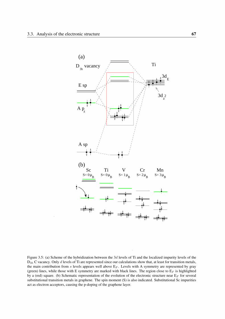
3.3. Analysis of the electronic structure 67
3hD vacancy
3d
E
3dz2
A sp
E sp
A pz
Ti
(a)
µB
S= 0
(b)Sc
µB
S= 3µB
S= 2µB
S= 1µB
S= 0Mn CrVTi
Figure 3.5: (a) Scheme of the hybridization between the 3d levels of Ti and the localized impurity levels of theD3h C vacancy. Only d levels of Ti are represented since our calculations show that, at least for transition metals,the main contribution from s levels appears well above EF . Levels with A symmetry are represented by gray(green) lines, while those with E symmetry are marked with black lines. The region close to EF is highlightedby a (red) square. (b) Schematic representation of the evolution of the electronic structure near EF for severalsubstitutional transition metals in graphene. The spin moment (S) is also indicated. Substitutional Sc impuritiesact as electron acceptors, causing the p-doping of the graphene layer.
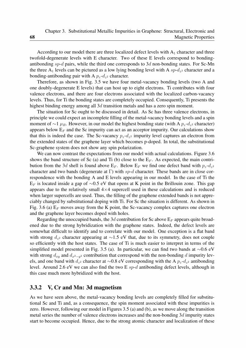
68Chapter 3. Substitutional Metallic Impurities in Graphene: Structural, Electronic and
Magnetic Properties
According to our model there are three localized defect levels with A1 character and threetwofold-degenerate levels with E character. Two of these E levels correspond to bonding-antibonding sp-d pairs, while the third one corresponds to 3d non-bonding states. For Sc-Mnthe three A1 levels can be pictured as a low lying bonding level with A sp-dz2 character and abonding-antibonding pair with A pz-dz2 character.
Therefore, as shown in Fig. 3.5 we have four metal-vacancy bonding levels (two A andone doubly-degenerate E levels) that can host up to eight electrons. Ti contributes with fourvalence electrons, and there are four electrons associated with the localized carbon-vacancylevels. Thus, for Ti the bonding states are completely occupied. Consequently, Ti presents thehighest binding energy among all 3d transition metals and has a zero spin moment.
The situation for Sc ought to be discussed in detail. As Sc has three valence electrons, inprinciple we could expect an incomplete filling of the metal-vacancy bonding levels and a spinmoment of ∼1 µB. However, in our model the highest bonding state (with A pz-dz2 character)appears below EF and the Sc impurity can act as an acceptor impurity. Our calculations showthat this is indeed the case. The Sc-vacancy pz-dz2 impurity level captures an electron fromthe extended states of the graphene layer which becomes p-doped. In total, the substitutionalSc-graphene system does not show any spin polarization.
We can now contrast the expectations from our model with actual calculations. Figure 3.6shows the band structure of Sc (a) and Ti (b) close to the EF . As expected, the main contri-bution from the 3d shell is found above EF . Below EF we find one defect band with pz-dz2
character and two bands (degenerate at Γ) with sp-d character. These bands are in close cor-respondence with the bonding A and E levels appearing in our model. In the case of Ti theEF is located inside a gap of ∼0.5 eV that opens at K point in the Brillouin zone. This gapappears due to the relatively small 4×4 supercell used in these calculations and is reducedwhen larger supercells are used. Thus, the filling of the graphene extended bands is not appre-ciably changed by substitutional doping with Ti. For Sc the situation is different. As shown inFig. 3.6 (a) EF moves away from the K point, the Sc-vacancy complex captures one electronand the graphene layer becomes doped with holes.
Regarding the unoccupied bands, the 3d contribution for Sc above EF appears quite broad-ened due to the strong hybridization with the graphene states. Indeed, the defect levels aresomewhat difficult to identify and to correlate with our model. One exception is a flat bandwith strong dz2 character appearing at ∼1.5 eV that, due to its symmetry, does not coupleso efficiently with the host states. The case of Ti is much easier to interpret in terms of thesimplified model presented in Fig. 3.5 (a). In particular, we can find two bands at ∼0.6 eVwith strong dxy and dx2−y2 contribution that correspond with the non-bonding d impurity lev-els, and one band with dz2 character at ∼0.8 eV corresponding with the A pz-dz2 antibondinglevel. Around 2.6 eV we can also find the two E sp-d antibonding defect levels, although inthis case much more hybridized with the host.
3.3.2 V, Cr and Mn: 3d magnetismAs we have seen above, the metal-vacancy bonding levels are completely filled for substitu-tional Sc and Ti and, as a consequence, the spin moment associated with these impurities iszero. However, following our model in Figures 3.5 (a) and (b), as we move along the transitionmetal series the number of valence electrons increases and the non-bonding 3d impurity statesstart to become occupied. Hence, due to the strong atomic character and localization of these
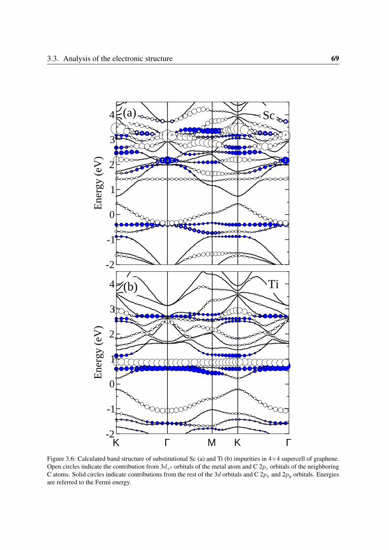
3.3. Analysis of the electronic structure 69
-2
-1
0
1
2
3
4
Ene
rgy
(eV
)
(a) Sc
Κ Γ Μ Κ Γ-2
-1
0
1
2
3
4
Ene
rgy
(eV
)
(b) Ti
Figure 3.6: Calculated band structure of substitutional Sc (a) and Ti (b) impurities in 4×4 supercell of graphene.Open circles indicate the contribution from 3dz2 orbitals of the metal atom and C 2pz orbitals of the neighboringC atoms. Solid circles indicate contributions from the rest of the 3d orbitals and C 2px and 2py orbitals. Energiesare referred to the Fermi energy.
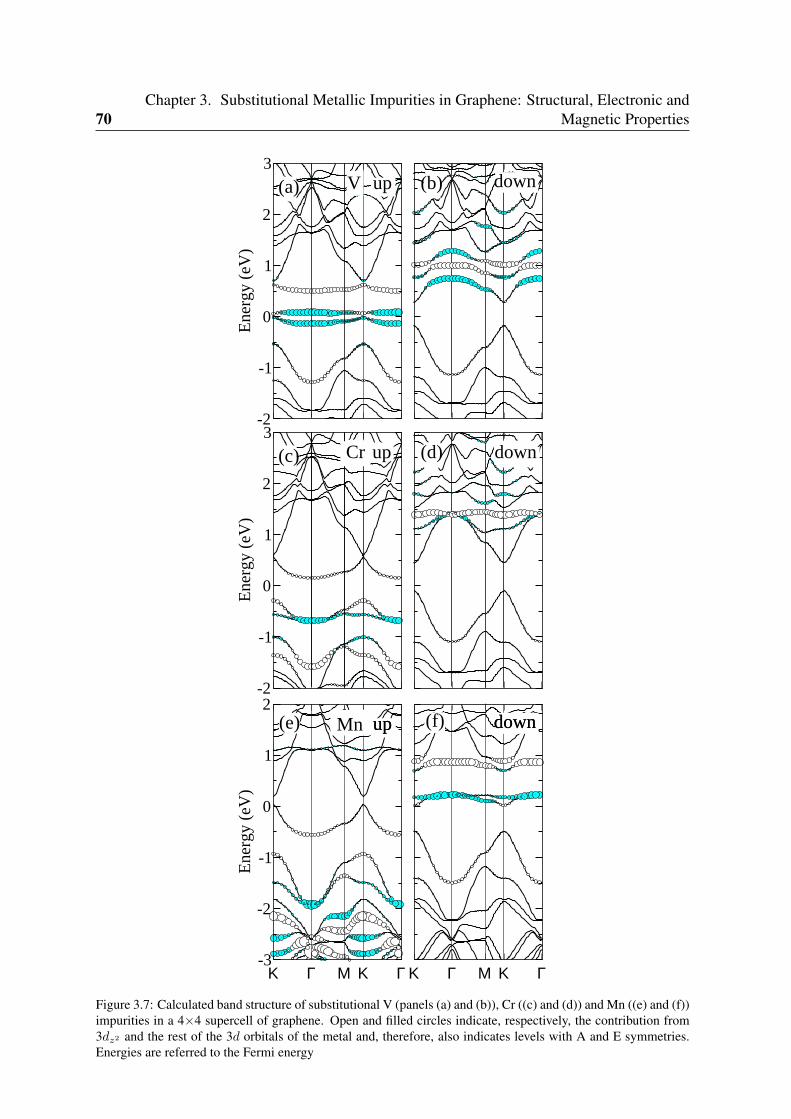
70Chapter 3. Substitutional Metallic Impurities in Graphene: Structural, Electronic and
Magnetic Properties
-2
-1
0
1
2
3
Ene
rgy
(eV
)
(a) V up (b) down
-2
-1
0
1
2
3
Ene
rgy
(eV
)
(c) Cr up (d) down
Κ Γ Μ Κ Γ-3
-2
-1
0
1
2
Ene
rgy
(eV
)
Κ Γ Μ Κ Γ
(e) up (f) downMn up down
Figure 3.7: Calculated band structure of substitutional V (panels (a) and (b)), Cr ((c) and (d)) and Mn ((e) and (f))impurities in a 4×4 supercell of graphene. Open and filled circles indicate, respectively, the contribution from3dz2 and the rest of the 3d orbitals of the metal and, therefore, also indicates levels with A and E symmetries.Energies are referred to the Fermi energy
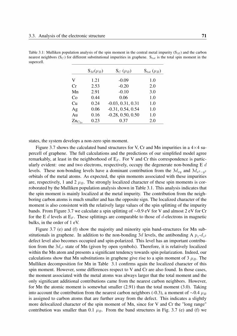
3.3. Analysis of the electronic structure 71
Table 3.1: Mulliken population analysis of the spin moment in the central metal impurity (SM ) and the carbonnearest neighbors (SC) for different substitutional impurities in graphene. Stot is the total spin moment in thesupercell.
SM (µB) SC (µB) Stot (µB)
V 1.21 -0.09 1.0Cr 2.53 -0.20 2.0Mn 2.91 -0.10 3.0Co 0.44 0.06 1.0Cu 0.24 -0.03, 0.31, 0.31 1.0Ag 0.06 -0.31, 0.54, 0.54 1.0Au 0.16 -0.28, 0.50, 0.50 1.0ZnC3v 0.23 0.37 2.0
states, the system develops a non-zero spin moment.Figure 3.7 shows the calculated band structures for V, Cr and Mn impurities in a 4×4 su-
percell of graphene. The full calculations and the predictions of our simplified model agreeremarkably, at least in the neighborhood of EF . For V and Cr this correspondence is partic-ularly evident: one and two electrons, respectively, occupy the degenerate non-bonding E dlevels. These non-bonding levels have a dominant contribution from the 3dxy and 3dx2−y2
orbitals of the metal atoms. As expected, the spin moments associated with these impuritiesare, respectively, 1 and 2 µB. The strongly localized character of these spin moments is cor-roborated by the Mulliken population analysis shown in Table 3.1. This analysis indicates thatthe spin moment is mainly localized at the metal impurity. The contribution from the neigh-boring carbon atoms is much smaller and has the opposite sign. The localized character of themoment is also consistent with the relatively large values of the spin splitting of the impuritybands. From Figure 3.7 we calculate a spin splitting of ∼0.9 eV for V and almost 2 eV for Crfor the E d levels at EF . These splittings are comparable to those of d-electrons in magneticbulks, in the order of 1 eV.
Figure 3.7 (e) and (f) show the majority and minority spin band-structures for Mn sub-stitutionals in graphene. In addition to the non-bonding 3d levels, the antibonding A pz-dz2
defect level also becomes occupied and spin-polarized. This level has an important contribu-tion from the 3dz2 state of Mn (given by open symbols). Therefore, it is relatively localizedwithin the Mn atom and presents a significant tendency towards spin polarization. Indeed, ourcalculations show that Mn substitutions in graphene give rise to a spin moment of 3 µB. TheMulliken decomposition for Mn in Table 3.1 confirms again the localized character of thisspin moment. However, some differences respect to V and Cr are also found. In those cases,the moment associated with the metal atoms was always larger that the total moment and theonly significant additional contributions came from the nearest carbon neighbors. However,for Mn the atomic moment is somewhat smaller (2.91) than the total moment (3.0). Takinginto account the contribution from the nearest carbon neighbors (-0.3), a moment of ∼0.4 µB
is assigned to carbon atoms that are further away from the defect. This indicates a slightlymore delocalized character of the spin moment of Mn, since for V and Cr the "long range"contribution was smaller than 0.1 µB. From the band structures in Fig. 3.7 (e) and (f) we
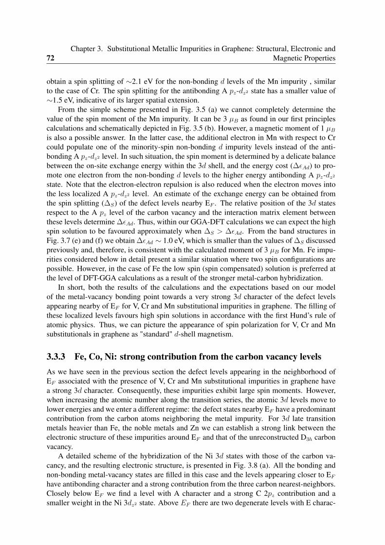
72Chapter 3. Substitutional Metallic Impurities in Graphene: Structural, Electronic and
Magnetic Properties
obtain a spin splitting of ∼2.1 eV for the non-bonding d levels of the Mn impurity , similarto the case of Cr. The spin splitting for the antibonding A pz-dz2 state has a smaller value of∼1.5 eV, indicative of its larger spatial extension.
From the simple scheme presented in Fig. 3.5 (a) we cannot completely determine thevalue of the spin moment of the Mn impurity. It can be 3 µB as found in our first principlescalculations and schematically depicted in Fig. 3.5 (b). However, a magnetic moment of 1 µB
is also a possible answer. In the latter case, the additional electron in Mn with respect to Crcould populate one of the minority-spin non-bonding d impurity levels instead of the anti-bonding A pz-dz2 level. In such situation, the spin moment is determined by a delicate balancebetween the on-site exchange energy within the 3d shell, and the energy cost (∆ϵAd) to pro-mote one electron from the non-bonding d levels to the higher energy antibonding A pz-dz2
state. Note that the electron-electron repulsion is also reduced when the electron moves intothe less localized A pz-dz2 level. An estimate of the exchange energy can be obtained fromthe spin splitting (∆S) of the defect levels nearby EF . The relative position of the 3d statesrespect to the A pz level of the carbon vacancy and the interaction matrix element betweenthese levels determine ∆ϵAd. Thus, within our GGA-DFT calculations we can expect the highspin solution to be favoured approximately when ∆S > ∆ϵAd. From the band structures inFig. 3.7 (e) and (f) we obtain ∆ϵAd ∼ 1.0 eV, which is smaller than the values of ∆S discussedpreviously and, therefore, is consistent with the calculated moment of 3 µB for Mn. Fe impu-rities considered below in detail present a similar situation where two spin configurations arepossible. However, in the case of Fe the low spin (spin compensated) solution is preferred atthe level of DFT-GGA calculations as a result of the stronger metal-carbon hybridization.
In short, both the results of the calculations and the expectations based on our modelof the metal-vacancy bonding point towards a very strong 3d character of the defect levelsappearing nearby of EF for V, Cr and Mn substitutional impurities in graphene. The filling ofthese localized levels favours high spin solutions in accordance with the first Hund’s rule ofatomic physics. Thus, we can picture the appearance of spin polarization for V, Cr and Mnsubstitutionals in graphene as "standard" d-shell magnetism.
3.3.3 Fe, Co, Ni: strong contribution from the carbon vacancy levelsAs we have seen in the previous section the defect levels appearing in the neighborhood ofEF associated with the presence of V, Cr and Mn substitutional impurities in graphene havea strong 3d character. Consequently, these impurities exhibit large spin moments. However,when increasing the atomic number along the transition series, the atomic 3d levels move tolower energies and we enter a different regime: the defect states nearby EF have a predominantcontribution from the carbon atoms neighboring the metal impurity. For 3d late transitionmetals heavier than Fe, the noble metals and Zn we can establish a strong link between theelectronic structure of these impurities around EF and that of the unreconstructed D3h carbonvacancy.
A detailed scheme of the hybridization of the Ni 3d states with those of the carbon va-cancy, and the resulting electronic structure, is presented in Fig. 3.8 (a). All the bonding andnon-bonding metal-vacancy states are filled in this case and the levels appearing closer to EF
have antibonding character and a strong contribution from the three carbon nearest-neighbors.Closely below EF we find a level with A character and a strong C 2pz contribution and asmaller weight in the Ni 3dz2 state. Above EF there are two degenerate levels with E charac-
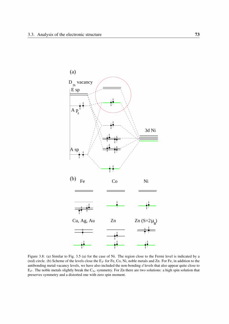
3.3. Analysis of the electronic structure 73
3d Ni
3hD vacancy
Co
Cu, Ag, Au µΒ
Zn (S=2 )Zn
NiFe(b)
A sp
A pz
E sp
(a)
Figure 3.8: (a) Similar to Fig. 3.5 (a) for the case of Ni. The region close to the Fermi level is indicated by a(red) circle. (b) Scheme of the levels close the EF for Fe, Co, Ni, noble metals and Zn. For Fe, in addition to theantibonding metal-vacancy levels, we have also included the non-bonding d levels that also appear quite close toEF . The noble metals slightly break the C3v symmetry. For Zn there are two solutions: a high spin solution thatpreserves symmetry and a distorted one with zero spin moment.
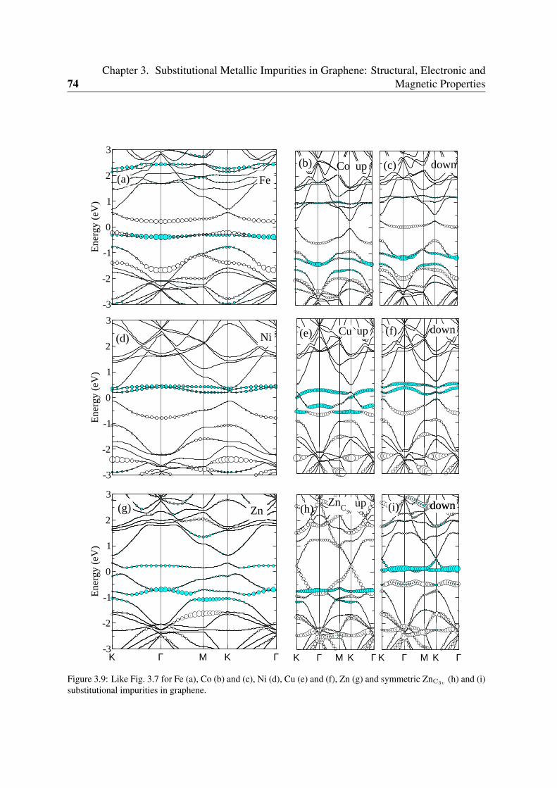
74Chapter 3. Substitutional Metallic Impurities in Graphene: Structural, Electronic and
Magnetic Properties
-3
-2
-1
0
1
2
3
Ene
rgy
(eV
)
(a) Fe
-3
-2
-1
0
1
2
3
Ene
rgy
(eV
)
(d) Ni
Κ Γ Μ Κ Γ-3
-2
-1
0
1
2
3
Ene
rgy
(eV
)
Zn(g)
Κ Γ Μ Κ Γ Κ Γ Μ Κ Γ
(h)Zn
C3v
up (i) downdown
Cu(e) up (f) down
(b) Co up (c) down
Figure 3.9: Like Fig. 3.7 for Fe (a), Co (b) and (c), Ni (d), Cu (e) and (f), Zn (g) and symmetric ZnC3v (h) and (i)substitutional impurities in graphene.
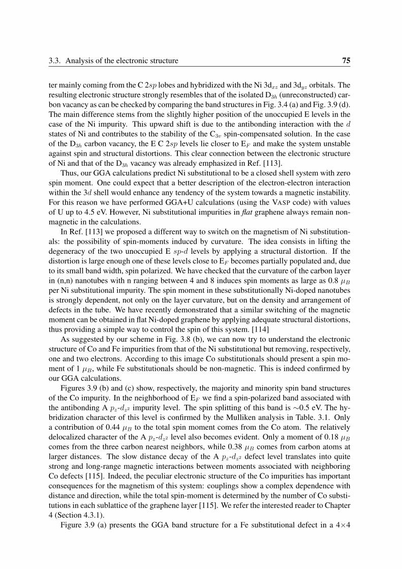
3.3. Analysis of the electronic structure 75
ter mainly coming from the C 2sp lobes and hybridized with the Ni 3dxz and 3dyz orbitals. Theresulting electronic structure strongly resembles that of the isolated D3h (unreconstructed) car-bon vacancy as can be checked by comparing the band structures in Fig. 3.4 (a) and Fig. 3.9 (d).The main difference stems from the slightly higher position of the unoccupied E levels in thecase of the Ni impurity. This upward shift is due to the antibonding interaction with the dstates of Ni and contributes to the stability of the C3v spin-compensated solution. In the caseof the D3h carbon vacancy, the E C 2sp levels lie closer to EF and make the system unstableagainst spin and structural distortions. This clear connection between the electronic structureof Ni and that of the D3h vacancy was already emphasized in Ref. [113].
Thus, our GGA calculations predict Ni substitutional to be a closed shell system with zerospin moment. One could expect that a better description of the electron-electron interactionwithin the 3d shell would enhance any tendency of the system towards a magnetic instability.For this reason we have performed GGA+U calculations (using the VASP code) with valuesof U up to 4.5 eV. However, Ni substitutional impurities in flat graphene always remain non-magnetic in the calculations.
In Ref. [113] we proposed a different way to switch on the magnetism of Ni substitution-als: the possibility of spin-moments induced by curvature. The idea consists in lifting thedegeneracy of the two unoccupied E sp-d levels by applying a structural distortion. If thedistortion is large enough one of these levels close to EF becomes partially populated and, dueto its small band width, spin polarized. We have checked that the curvature of the carbon layerin (n,n) nanotubes with n ranging between 4 and 8 induces spin moments as large as 0.8 µB
per Ni substitutional impurity. The spin moment in these substitutionally Ni-doped nanotubesis strongly dependent, not only on the layer curvature, but on the density and arrangement ofdefects in the tube. We have recently demonstrated that a similar switching of the magneticmoment can be obtained in flat Ni-doped graphene by applying adequate structural distortions,thus providing a simple way to control the spin of this system. [114]
As suggested by our scheme in Fig. 3.8 (b), we can now try to understand the electronicstructure of Co and Fe impurities from that of the Ni substitutional but removing, respectively,one and two electrons. According to this image Co substitutionals should present a spin mo-ment of 1 µB, while Fe substitutionals should be non-magnetic. This is indeed confirmed byour GGA calculations.
Figures 3.9 (b) and (c) show, respectively, the majority and minority spin band structuresof the Co impurity. In the neighborhood of EF we find a spin-polarized band associated withthe antibonding A pz-dz2 impurity level. The spin splitting of this band is ∼0.5 eV. The hy-bridization character of this level is confirmed by the Mulliken analysis in Table. 3.1. Onlya contribution of 0.44 µB to the total spin moment comes from the Co atom. The relativelydelocalized character of the A pz-dz2 level also becomes evident. Only a moment of 0.18 µB
comes from the three carbon nearest neighbors, while 0.38 µB comes from carbon atoms atlarger distances. The slow distance decay of the A pz-dz2 defect level translates into quitestrong and long-range magnetic interactions between moments associated with neighboringCo defects [115]. Indeed, the peculiar electronic structure of the Co impurities has importantconsequences for the magnetism of this system: couplings show a complex dependence withdistance and direction, while the total spin-moment is determined by the number of Co substi-tutions in each sublattice of the graphene layer [115]. We refer the interested reader to Chapter4 (Section 4.3.1).
Figure 3.9 (a) presents the GGA band structure for a Fe substitutional defect in a 4×4
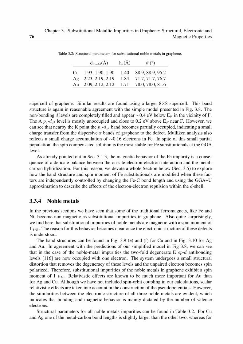
76Chapter 3. Substitutional Metallic Impurities in Graphene: Structural, Electronic and
Magnetic Properties
Table 3.2: Structural parameters for substitutional noble metals in graphene.
dC−M(Å) hz(Å) θ ()
Cu 1.93, 1.90, 1.90 1.40 88.9, 88.9, 95.2Ag 2.23, 2.19, 2.19 1.84 71.7, 71.7, 76.7Au 2.09, 2.12, 2.12 1.71 78.0, 78.0, 81.6
supercell of graphene. Similar results are found using a larger 8×8 supercell. This bandstructure is again in reasonable agreement with the simple model presented in Fig. 3.8. Thenon-bonding d levels are completely filled and appear ∼0.4 eV below EF in the vicinity of Γ.The A pz-dz2 level is mostly unoccupied and close to 0.2 eV above EF near Γ. However, wecan see that nearby the K point the pz-dz2 band becomes partially occupied, indicating a smallcharge transfer from the dispersive π bands of graphene to the defect. Mulliken analysis alsoreflects a small charge accumulation of ∼0.16 electrons in Fe. In spite of this small partialpopulation, the spin compensated solution is the most stable for Fe substitutionals at the GGAlevel.
As already pointed out in Sec. 3.1.3, the magnetic behavior of the Fe impurity is a conse-quence of a delicate balance between the on-site electron-electron interaction and the metal-carbon hybridization. For this reason, we devote a whole Section below (Sec. 3.5) to explorehow the band structure and spin moment of Fe substitutionals are modified when these fac-tors are independently controlled by changing the Fe-C bond length and using the GGA+Uapproximation to describe the effects of the electron-electron repulsion within the d-shell.
3.3.4 Noble metalsIn the previous sections we have seen that some of the traditional ferromagnets, like Fe andNi, become non-magnetic as substitutional impurities in graphene. Also quite surprisingly,we find here that substitutional impurities of noble metals are magnetic with a spin moment of1 µB. The reason for this behavior becomes clear once the electronic structure of these defectsis understood.
The band structures can be found in Fig. 3.9 (e) and (f) for Cu and in Fig. 3.10 for Agand Au. In agreement with the predictions of our simplified model in Fig 3.8, we can seethat in the case of the noble-metal impurities the two-fold degenerate E sp-d antibondinglevels [116] are now occupied with one electron. The system undergoes a small structuraldistortion that removes the degeneracy of these levels and the unpaired electron becomes spinpolarized. Therefore, substitutional impurities of the noble metals in graphene exhibit a spinmoment of 1 µB. Relativistic effects are known to be much more important for Au thanfor Ag and Cu. Although we have not included spin-orbit coupling in our calculations, scalarrelativistic effects are taken into account in the construction of the pseudopotentials. However,the similarities between the electronic structure of all three noble metals are evident, whichindicates that bonding and magnetic behavior is mainly dictated by the number of valenceelectrons.
Structural parameters for all noble metals impurities can be found in Table 3.2. For Cuand Ag one of the metal-carbon bond lengths is slightly larger than the other two, whereas for
3.3. Analysis of the electronic structure 77
-2
-1
0
1
2
3E
nerg
y (e
V)
(a) Ag up (b) down
Κ Γ Μ Κ Γ-2
-1
0
1
2
3
Ene
rgy
(eV
)
Κ Γ Μ Κ Γ
(c) Au up (d) down
Figure 3.10: Like Fig. 3.7 for Ag and Au. The similarities with the band structure of Cu in Fig. 3.9 are evident.
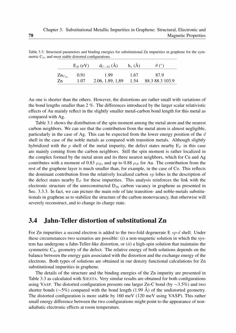
78Chapter 3. Substitutional Metallic Impurities in Graphene: Structural, Electronic and
Magnetic Properties
Table 3.3: Structural parameters and binding energies for substitutional Zn impurities in graphene for the sym-metric C3v and most stable distorted configurations.
EB (eV) dC−M (Å) hz (Å) θ ()
ZnC3v 0.91 1.99 1.67 87.9Zn 1.07 2.06, 1.89, 1,89 1.54 88.3 88.3 103.9
Au one is shorter than the others. However, the distortions are rather small with variations ofthe bond lengths smaller than 2 %. The differences introduced by the larger scalar relativisticeffects of Au mainly reflect in the slightly smaller metal-carbon bond length for this metal ascompared with Ag.
Table 3.1 shows the distribution of the spin moment among the metal atom and the nearestcarbon neighbors. We can see that the contribution from the metal atom is almost negligible,particularly in the case of Ag. This can be expected from the lower energy position of the dshell in the case of the noble metals as compared with transition metals. Although slightlyhybridized with the p shell of the metal impurity, the defect states nearby EF in this caseare mainly coming from the carbon neighbors. Still the spin moment is rather localized inthe complex formed by the metal atom and its three nearest neighbors, which for Cu and Agcontributes with a moment of 0.83 µB, and up to 0.88 µB for Au. The contribution from therest of the graphene layer is much smaller than, for example, in the case of Co. This reflectsthe dominant contribution from the relatively localized carbon sp lobes in the description ofthe defect states nearby EF for these impurities. This analysis reinforces the link with theelectronic structure of the unreconstructed D3h carbon vacancy in graphene as presented inSec. 3.3.3. In fact, we can picture the main role of late transition- and noble-metals substitu-tionals in graphene as to stabilize the structure of the carbon monovacancy, that otherwise willseverely reconstruct, and to change its charge state.
3.4 Jahn-Teller distortion of substitutional Zn
For Zn impurities a second electron is added to the two-fold degenerate E sp-d shell. Underthese circumstances two scenarios are possible: (i) a non-magnetic solution in which the sys-tem has undergone a Jahn-Teller-like distortion, or (ii) a high-spin solution that maintains thesymmetric C3v geometry of the defect. The relative energy of both solutions depends on thebalance between the energy gain associated with the distortion and the exchange energy of theelectrons. Both types of solutions are obtained in our density functional calculations for Znsubstitutional impurities in graphene.
The details of the structure and the binding energies of the Zn impurity are presented inTable 3.3 as calculated with SIESTA. Very similar results are obtained for both configurationsusing VASP. The distorted configuration presents one larger Zn-C bond (by ∼3.5%) and twoshorter bonds (∼5%) compared with the bond length (1.99 Å) of the undistorted geometry.The distorted configuration is more stable by 160 meV (120 meV using VASP). This rathersmall energy difference between the two configurations might point to the appearance of non-adiabatic electronic effects at room temperature.
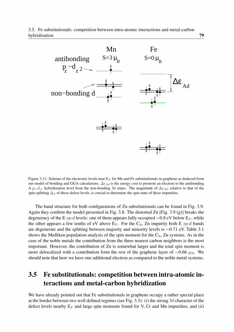
3.5. Fe substitutionals: competition between intra-atomic interactions and metal-carbonhybridization 79
µB
S=3Mn
antibondingp −d
zz 2
non−bonding d
µB
S=0
∆εAd
Fe
Figure 3.11: Scheme of the electronic levels near EF for Mn and Fe substitutionals in graphene as deduced fromour model of bonding and GGA calculations. ∆ϵAd is the energy cost to promote an electron to the antibondingA pz-dz2 hybridization level from the non-bonding 3d states. The magnitude of ∆ϵAd, relative to that of thespin-splitting ∆S of these defect levels, is crucial to determine the spin state of these impurities.
The band structure for both configurations of Zn substitutionals can be found in Fig. 3.9.Again they confirm the model presented in Fig. 3.8. The distorted Zn [Fig. 3.9 (g)] breaks thedegeneracy of the E sp-d levels: one of them appears fully occupied ∼0.8 eV below EF , whilethe other appears a few tenths of eV above EF . For the C3v Zn impurity both E sp-d bandsare degenerate and the splitting between majority and minority levels is ∼0.71 eV. Table 3.1shows the Mulliken population analysis of the spin moment for the C3v Zn systems. As in thecase of the noble metals the contribution from the three nearest carbon neighbors is the mostimportant. However, the contribution of Zn is somewhat larger and the total spin moment ismore delocalized with a contribution form the rest of the graphene layer of ∼0.66 µB. Weshould note that here we have one additional electron as compared to the noble metal systems.
3.5 Fe substitutionals: competition between intra-atomic in-teractions and metal-carbon hybridization
We have already pointed out that Fe substitutionals in graphene occupy a rather special placeat the border between two well defined regimes (see Fig. 3.3): (i) the strong 3d character of thedefect levels nearby EF and large spin moments found for V, Cr and Mn impurities, and (ii)
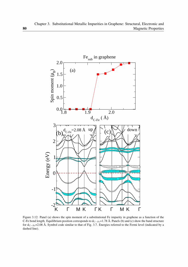
80Chapter 3. Substitutional Metallic Impurities in Graphene: Structural, Electronic and
Magnetic Properties
1.8 1.9 2.0d
C-Fe ( Å)
0.0
0.5
1.0
1.5
2.0
Spi
n m
omen
t (µB)
Fesub
in graphene
(a)
Κ Γ Μ Κ Γ-2
-1
0
1
2
3
Ene
rgy
(eV
)
Κ Γ Μ Κ Γ
dC-Fe
=2.08 Å (c)(b)up down
Figure 3.12: Panel (a) shows the spin moment of a substitutional Fe impurity in graphene as a function of theC-Fe bond length. Equilibrium position corresponds to dC−Fe=1.78 Å. Panels (b) and (c) show the band structurefor dC−Fe=2.08 Å. Symbol code similar to that of Fig. 3.7. Energies referred to the Fermi level (indicated by adashed line).
3.5. Fe substitutionals: competition between intra-atomic interactions and metal-carbonhybridization 81
the larger carbon character of those electronic levels and the small oscillatory spin-momentsof Co, Ni and the noble metals. GGA calculations [Fig. 3.9 (a)] locate Fe impurities within thesecond group, with all the 3d non-bonding levels fully occupied and non-magnetic. Thus, thespin moment drops from 3 µB for Mn impurities to zero for Fe, showing a quite discontinuousbehavior as a function of the number of valence electrons. In analogy with the standard Slater-Pauling rule for transition metals, one could expect to find a more gradual decrease of the spinmoment as the number of valence electrons is increased, i.e. Fe would have a moment of 2 µB.In the present section we study in detail why the non-magnetic solution is more stable for Fe.
3.5.1 Key parameters: metal-carbon hopping and intra-atomic Coulombinteractions
Figure 3.11 shows a scheme of the electronic structure of both Mn and Fe defects. Dependingon how electrons are arranged among the A pz-dz2 antibonding level and the non-bonding 3dstates, Mn can exhibit spin moments of 3 µB or 1 µB, while Fe can have a moment of 2 µB
or can be non-magnetic. At the GGA level Mn prefers the high-spin configuration, while thelow-spin one is more stable for Fe. As commented in the Section 3.3.2, the relative stabilityof the different spin states depends on the balance between the effects of Coulomb repulsionand exchange within the 3d levels and the relative energy position of the impurity levels givenby ∆ϵAd (see Fig. 3.11). The hybridization with the neighboring C atoms is crucial in thisinterplay since it influences (i) the degree of localization of the defect levels and the screeningof Coulomb interactions, which modify the spin splitting of the electronic levels ∆S , and (ii)the value of ∆ϵAd through the effective hopping parameter between the 3d states and the A pz
carbon vacancy level. Next, we shall deal with both aspects for substitutional Fe in graphene.
Changing Fe-graphene hopping with distance.
By tuning the interaction with the host structure it should be possible to change the spin mo-ment of these impurities. We can modify the hopping by artificially changing Fe-graphenedistance. The results of such calculation are shown in Fig. 3.12 (a). While maintaining thethree-fold symmetry of the system, we have performed a series of calculations by progres-sively increasing the height of the Fe atom over the graphene layer. Increasing the C-Fe bondlength by ∼9% we observe an abrupt jump of the spin moment from zero to 1.5 µB. Thespin moment continues to rise and saturates at a value of 2.0 µB for dC−Fe∼2.07 Å. Thisconvincingly shows that the metal-carbon hybridization is the key parameter to explain thenon-magnetic state of Fe substitutional impurity in graphene. When increasing the C-Fe dis-tance we mainly decrease ∆ϵAd. Thus, we reduce the energy penalty for promoting electronsfrom the non-bonding d to the A pz-dz2 defect levels. At the same time we also increase theatomic character of the non-bonding d states and reduce the effect of the screening due to theelectrons in the graphene layer. This ∆ϵAd reduction promotes the electron-electron repulsionwithin the 3d states of Fe and, eventually, stabilizes the solution with 2.0 µB.
Figures 3.12 (b) and (c) present the band structure for the high-spin state of Fe, wherethe C-Fe bond length has been elongated up to 2.08 Å. We notice the differences with thespin-compensated ground state in Fig. 3.9 (a). On the one hand, one electron is promotedfrom the non-bonding d states to the more delocalized antibonding A pz-dz2 impurity level in
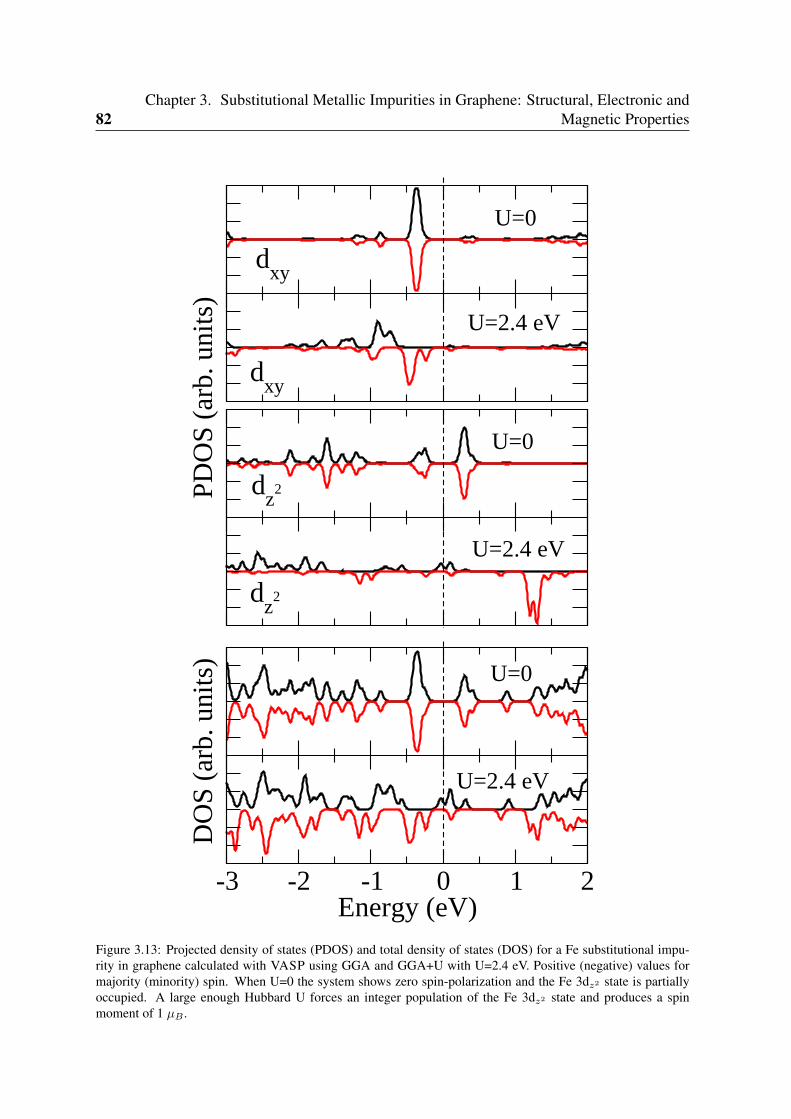
82Chapter 3. Substitutional Metallic Impurities in Graphene: Structural, Electronic and
Magnetic Properties
PDO
S (a
rb. u
nits
)
-3 -2 -1 0 1 2Energy (eV)
DO
S (a
rb. u
nits
)
dxy
dz
2
U=0
U=2.4 eV
U=0
dxy
U=2.4 eV
U=0
dz
2
U=2.4 eV
Figure 3.13: Projected density of states (PDOS) and total density of states (DOS) for a Fe substitutional impu-rity in graphene calculated with VASP using GGA and GGA+U with U=2.4 eV. Positive (negative) values formajority (minority) spin. When U=0 the system shows zero spin-polarization and the Fe 3dz2 state is partiallyoccupied. A large enough Hubbard U forces an integer population of the Fe 3dz2 state and produces a spinmoment of 1 µB .
3.5. Fe substitutionals: competition between intra-atomic interactions and metal-carbonhybridization 83
order to reduce the effect of electron-electron repulsion. On the other hand, the spin momentis maximized in accordance with Hund’s first rule.
Therefore, we have seen that the non-magnetic character of the Fe substitutionals in theGGA calculations is due to the larger interaction with the graphene layer, as compared forexample with the Mn impurity. This is consistent with the fact that Fe, together with Co andNi, presents the smaller carbon metal bond length among the whole series of 3d transitionmetals. Fe impurities also have one of the largest binding energies. By artificially reducingthis interaction it could be possible to obtain magnetic Fe substitutional impurities in graphene.
Changing intra-atomic Coulomb interaction U.
Another route to explore would be to increase the size of intra-atomic electron-electron inter-actions. We have done so by using the so-called GGA+U methodology in which a Hubbardterm is explicitly added to the DFT Hamiltonian and solved within the mean-field approxi-mation. Our results indicate that with a reasonable value of U (∼2 eV or larger) we obtain amagnetic solution for Fe substitutionals. However, contrary to our initial expectation this solu-tion does not correspond to the 2 µB high-spin solution discussed above, but to a new solutionwith 1 µB. The key reason to understand this behavior is the partial occupation of the Fe 3dz2
state at the level of GGA calculations. The dz2 state is strongly coupled to the delocalized Apz vacancy level appearing nearby EF and both, this hybridization and the population of theatomic orbital, are strongly modified when the value of U is increased.
Figure 3.13 shows the results of the electronic structure of Fe impurities calculated usingGGA+U with U=2.4 eV and compared with those with U=0. The two upper panels show theprojected density of states (PDOS) onto the dxy orbital (the projection onto the dx2−y2 orbitalis identical by symmetry), the two middle panels show the PDOS onto the dz2 orbital of Feand the two lower panels the total density of states. At the level of GGA, with U=0, thereis a very well defined peak closely below EF in the dxy PDOS corresponding to the positionof the non-bonding d states. The spectral weight coming from the dz2 orbital is more spread:presents some broad structure around −1.5 eV corresponding to the bonding A pz-dz2 defectlevel interacting with the valence band of graphene, and a narrower peak near EF with originin the slightly occupied antibonding A pz-dz2 impurity state. Therefore, from the Fe 3d statesappearing nearby EF we can picture the dxy and dx2−y2 states as fully occupied and the dz2 aspartially occupied due to the larger interaction with the carbon neighbors.
For a sufficiently large value of U the C 2pz-3dz2 hybridization is overcome by the ten-dency of the electrons to have an integer population within the localized 3d shell. Thus,the 3dz2 localizes one electron and, as a consequence, the system develops a 1 µB spin-polarization. This changes can be appreciated in Fig. 3.13. The majority-spin 3dz2 PDOSshifts downwards, while a strong unoccupied peak appears around 1.5 eV in the 3dz2 minorityspin PDOS. Simultaneously, a more delocalized level mostly coming from the 2pz orbitals ofthe neighboring C atoms appears half-filled at EF . Note that other levels, such as the dxy, donot suffer such strong modifications since they are already almost fully occupied with U=0. Itis also interesting to note that, due to symmetry considerations, they couple with the graphenelayer very differently from the dz2 level.
84Chapter 3. Substitutional Metallic Impurities in Graphene: Structural, Electronic and
Magnetic Properties
3.5.2 Relevance for recent experiments of Fe implantation in graphite
There are recent reports on the paramagnetism of iron-implanted graphite that indicate theexistence of local magnetic moments associated with the implanted Fe atoms. [117,118] Thiswould be in contradiction with the present GGA results if we assume that the Fe atoms areincorporated to the graphene layer as substitutionals. However, the final geometry of theimplanted atoms in these experiments is not known. Furthermore, a considerable amount ofdefects is created during the implantation process. Although it has been argued that a largepart of the damage is healed by vacancy-interstitial recombination [118], the influence ofthese defects, specially interstitials and big voids, on the observed magnetic response can bedeterminant.
Therefore, it is not fully clear if we can compare our calculations for Fe substitutionalimpurities in an otherwise perfect graphene layer with these experimental data. However,as we have shown in detail in this section, Fe substitutionals are very close to a transitionand, depending on the details of the calculations, it is possible to obtain a magnetic groundstate. In particular, Fe substitutionals develop a spin moment of 1 µB at the level of GGA+Ucalculations for reasonable values of the U parameter. This might be an indication that thenon-magnetic ground state found in GGA calculations is a consequence of the limitations ofthe used functionals.
3.6 Conclusions
We have presented a DFT study of the structure, energetics, and electronic and magnetic prop-erties of several metal atoms as substitutional impurities in graphene, i.e., bound to a carbonmonovacancy in the layer. We have considered the cases of all 3d transition metals, noblemetals and Zn. We have paid special attention to their electronic and magnetic properties anddevelop a simple model to understand the observed trends. Our model is based on the hy-bridization of the states of the metal atoms with those of an unreconstructed carbon vacancy.The main ingredients of the model are the assumption, after our calculations, of a three-foldsymmetric bonding configuration and the approximate knowledge of the relative energy posi-tions of the levels of the carbon monovacancy and the d shell of the metal impurity as we movealong the transition series. With this model we can understand the observed the variations ofthe electronic structure of the defect, the size and localization of the spin moment, and thebinding energy. We have identified three different regimes corresponding to filling of carbon-metal hybridization shells with different character: bonding, non-bonding and antibonding.
In more detail:(i ) Most substitutional metal impurities present an almost perfectly symmetric three-fold
configuration with C3v symmetry. Noble metals slightly depart from this perfect configuration.Only Zn presents a considerable structural distortion.
(ii) For Sc and Ti the metal-carbon bonding shell is completely filled. Therefore, theseimpurities present the highest binding energies and zero spin moments. Sc substitutionals actas p-dopants for graphene: each Sc impurity localizes one extra electron from the carbon layer.
(iii) The non-bonding d shell becomes partially populated for V, Cr and Mn, which developa very localized spin-moment of 1, 2 and 3 µB, respectively. The binding energy decreasesslightly as the d shell moves to lower energies, thus reducing its hybridization with the higher
3.6. Conclusions 85
carbon vacancy levels.(iv) For Co, Ni, the noble metals and Zn, the metal-carbon levels are progressively popu-
lated. This gives rise to a oscillatory behavior of the spin moment between 0 and 1 µB. Thespin moments are more delocalized than those found for V, Cr and Mn and present a consider-able contribution from the carbon atoms around the impurity. The binding energy presents alocal maximum for Co, but suddenly drops for the noble metals and has its minimum for Zn.
(v) The electronic structure, nearby EF , of substitutional impurities of Co, Ni, the noblemetals and Zn has a strong resemblance to that of the unreconstructed D3h carbon monova-cancy. We can draw an analogy between the electronic structure of these impurities and thatof the unreconstructed D3h carbon monovacancy with different number of electrons (chargestates). The spin moment of these impurities can be fully understand exploiting this equiv-alence. In particular, the result that noble metals develop a spin moment of 1 µB emergesnaturally within this picture.
(vi) For the Co impurity, the equivalence can be pushed a step further and we can draw ananalogy with the electronic structure of a π-vacancy in a simple π-tight-binding description ofgraphene. This can be used to explain the peculiar behavior found for the magnetic couplingsbetween Co substitutionals in graphene. [115]
(vii) Fe impurities occupy a distinct position at the border between two different regimes.Their magnetic behavior stems from the competition between the carbon-metal hybridizationand the electron-electron interaction within the 3d shell. As a result, although Fe impuritiesare non-magnetic at the GGA level, GGA+U calculations with moderate values of U (above∼2 eV) produce a spin-moment of 1 µB.
(viii) We have found that the unexpected result that Au substitutionals [112,119] present aspin moment of 1µB also holds for all noble metals, i.e., also Ag and Cu present a 1 µB spinmoment.
(ix) We have found that the ground state of the Zn substitutional is non-magnetic due toa Jahn-Teller distortion. Yet, it is possible to stabilize a symmetric configuration with a spinmoment of 2µB with a very small energy penalty of ∼150 meV.
Substitutional impurities of metals in graphene present some interesting magnetic and elec-tronic properties and, therefore, can provide an interesting route to add functionalities or totune the response of devices based on graphenic materials. Furthermore, recent experimentsby Rodriguez-Manzo and Banhart [83] have demonstrated the possibility to create individ-ual vacancies at desired locations in carbon nanotubes using electron beams. This ability, incombination with the high stability of substitutional impurities, can open a route to fabricateordered arrays of these impurities at predefined locations. Such devices would allow, amongother applications, the experimental verification of the theoretical predictions of unusual mag-netic interactions mediated by graphene. [84, 85, 115]

86Chapter 3. Substitutional Metallic Impurities in Graphene: Structural, Electronic and
Magnetic Properties
Chapter 4
Real Systems that Behave Likeπ-Vacancies: Co Doping and CovalentFunctionalization
The peculiar electronic and magnetic properties of graphene monolayers have recently at-tracted much attention. New types of electronic and, particularly, spintronic devices basedon graphene have been proposed [7, 12, 20, 120]. These graphene structures also drive anincreasing interest to study defects, which are always expected in real-life devices. Intrin-sic defects have been already widely studied [12, 33, 45, 54, 121] and extrinsic defects, likesubstitutional atoms studied in the previous chapter, are presently under intense research.[53, 113, 115, 122–124]
In this chapter, we extend further our study of defects in graphene. We will explore otheralternatives to generate magnetism in graphene and carbon nanotubes using defects. We willalso examine the mechanisms of magnetic coupling between the spin moments linked to de-fects, giving details of the exchange interaction and its distance decay. We also extent theanalysis to organic and inorganic molecules chemisorbed on graphene and carbon nanotubes(CNTs). We show that all these calculations can be understood on the basis of a simple modelpresented in the Chapter 1, the so-called π−vacancy (see Section 1.6.1). This model capturesthe main features of the defects and the physics behind in a simple way. The present chapteris divided into four main sections: In Section 4.1 we introduce the π−vacancy model in thecontext of a graphene monolayer substitutionally doped with Co (Cosub) atoms. We observethat there is a one-to-one correspondence between the expected behavior for single vacanciesin a simple π-tight binding model of graphene and that found for the Cosub defects. The elec-tronic structure of the Cosub defect at the Fermi energy (EF ) is dominated by a level with astrong contribution from the pz orbitals of the neighboring C atoms. Moreover, each Cosub
defect shows a spin moment of 1.0 µB, partly divided between the metallic impurity and theC-neighbours. In sections 4.2 and 4.3 we focus on chemisorbed molecules on top of C ingraphene and nanotubes, respectively. We demonstrate that when a single covalent C-C bondis established between an adsorbate and a carbon atom in the graphitic structure, a spin mag-netic moment of 1.0 µB is induced in the system. This moment is largely independent of theparticular adsorbate. This effect occurs for organic and inorganic molecules.
In the fourth part, Section 4.4, we consider magnetic couplings. This is an important is-sue because it deals with the possibility to create spin order in graphene based on defects.
87
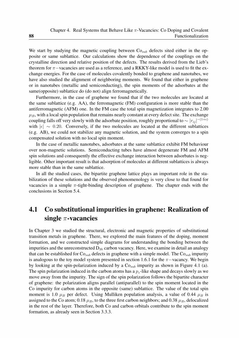
88Chapter 4. Real Systems that Behave Like π-Vacancies: Co Doping and Covalent
Functionalization
We start by studying the magnetic coupling between Cosub defects sited either in the op-posite or same sublattice. Our calculations show the dependence of the couplings on thecrystalline direction and relative position of the defects. The results derived from the Lieb’stheorem for π−vacancies are used as a reference, and a RKKY-like model is used to fit the ex-change energies. For the case of molecules covalently bonded to graphene and nanotubes, wehave also studied the alignment of neighboring moments. We found that either in grapheneor in nanotubes (metallic and semiconducting), the spin moments of the adsorbates at thesame(opposite) sublattice do (do not) align ferromagnetically.
Furthermore, in the case of graphene we found that if the two molecules are located atthe same sublattice (e.g. AA), the ferromagnetic (FM) configuration is more stable than theantiferromagnetic (AFM) one. In the FM case the total spin magnetization integrates to 2.00µB, with a local spin population that remains nearly constant at every defect site. The exchangecoupling falls off very slowly with the adsorbate position, roughly proportional to ∼ |rij|−(1+ϵ)
with |ϵ| ∼ 0.20. Conversely, if the two molecules are located at the different sublattices(e.g. AB), we could not stabilize any magnetic solution, and the system converges to a spincompensated solution with no local spin moment.
In the case of metallic nanotubes, adsorbates at the same sublattice exhibit FM behaviourover non-magnetic solutions. Semiconducting tubes have almost degenerate FM and AFMspin solutions and consequently the effective exchange interaction between adsorbates is neg-ligible. Other important result is that adsorption of molecules at different sublattices is alwaysmore stable than in the same sublattice.
In all the studied cases, the bipartite graphene lattice plays an important role in the sta-bilization of these solutions and the observed phenomenology is very close to that found forvacancies in a simple π-tight-binding description of graphene. The chapter ends with theconclusions in Section 5.4.
4.1 Co substitutional impurities in graphene: Realization ofsingle π-vacancies
In Chapter 3 we studied the structural, electronic and magnetic properties of substitutionaltransition metals in graphene. There, we explored the main features of the doping, momentformation, and we constructed simple diagrams for understanding the bonding between theimpurities and the unreconstructed D3h carbon vacancy. Here, we examine in detail an analogythat can be established for Cosub defects in graphene with a simple model. The Cosub impurityis analogous to the toy model system presented in section 1.6.1 for the π−vacancy. We beginby looking at the spin-polarization induced by a Cosub impurity as shown in Figure 4.1 (a).The spin polarization induced in the carbon atoms has a pz-like shape and decays slowly as wemove away from the impurity. The sign of the spin polarization follows the bipartite characterof graphene: the polarization aligns parallel (antiparallel) to the spin moment located in theCo impurity for carbon atoms in the opposite (same) sublattice. The value of the total spinmoment is 1.0 µB per defect. Using Mulliken population analysis, a value of 0.44 µB isassigned to the Co atom; 0.18 µB, to the three first carbon neighbors; and 0.38 µB, delocalizedin the rest of the layer. Therefore, both Co and carbon orbitals contribute to the spin momentformation, as already seen in Section 3.3.3.
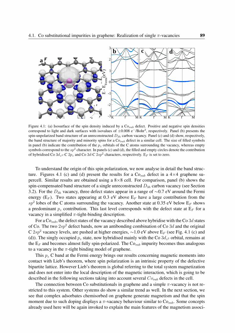
4.1. Co substitutional impurities in graphene: Realization of single π-vacancies 89
x y
z
a
-3
-2
-1
0
1
2
3
E -
EFe
rmi(e
V)
K MΓ MΓK
b
MΓK
c d
Figure 4.1: (a) Isosurface of the spin density induced by a Cosub defect. Positive and negative spin densitiescorrespond to light and dark surfaces with isovalues of ±0.008 e−/Bohr3, respectively. Panel (b) presents thespin-unpolarized band structure of an unreconstructed D3h carbon vacancy. Panel (c) and (d) show, respectively,the band structure of majority and minority spins for a Cosub defect in a similar cell. The size of filled symbolsin panel (b) indicate the contribution of the pz orbitals of the C atoms surrounding the vacancy, whereas emptysymbols correspond to the sp2 character. In panels (c) and (d), the filled and empty circles denote the contributionof hybridised Co 3dz2-C 2pz and Co 3d-C 2sp2 characters, respectively. EF is set to zero.
To understand the origin of this spin polarization, we now analyse in detail the band struc-ture. Figures 4.1 (c) and (d) present the results for a Cosub defect in a 4×4 graphene su-percell. Similar results are obtained using a 8×8 cell. For comparison, panel (b) shows thespin-compensated band structure of a single unreconstructed D3h carbon vacancy (see Section3.2). For the D3h vacancy, three defect states appear in a range of ∼0.7 eV around the Fermienergy (EF ). Two states appearing at 0.3 eV above EF have a large contribution from thesp2 lobes of the C atoms surrounding the vacancy. Another state at 0.35 eV below EF showsa predominant pz contribution. This last level corresponds with the defect state at EF for avacancy in a simplified π-tight-binding description.
For a Cosub, the defect states of the vacancy described above hybridise with the Co 3d statesof Co. The two 2sp2 defect bands, now an antibonding combination of Co 3d and the originalC 2sp2 vacancy levels, are pushed at higher energies, ∼1.0 eV above EF (see Fig. 4.1 (c) and(d)). The singly occupied pz state, now hybridised mainly with the Co 3dz2 orbital, remains atthe EF and becomes almost fully spin-polarized. The Cosub impurity becomes thus analogousto a vacancy in the π-tight binding model of graphene.
This pz C band at the Fermi energy brings our results concerning magnetic moments intocontact with Lieb’s theorem, where spin polarization is an intrinsic property of the defectivebipartite lattice. However Lieb’s theorem is global referring to the total system magnetizationand does not enter into the local description of the magnetic interaction, which is going to bedescribed in the following sections taking into account several Cosub defects in the cell.
The connection between Co substitutionals in graphene and a simple π-vacancy is not re-stricted to this system. Other systems do show a similar trend as well. In the next section, wesee that complex adsorbates chemisorbed on graphene generate magnetism and that the spinmoment due to such doping displays a π-vacancy behaviour similar to Cosub. Some conceptsalready used here will be again invoked to explain the main features of the magnetism associ-
90Chapter 4. Real Systems that Behave Like π-Vacancies: Co Doping and Covalent
Functionalization
ated with these defects, leading to an universal magnetic behaviour in graphene independentof the particular adsorbate.
4.2 Organic adsorbates chemisorbed on graphene: Univer-sal spin moment
Chemical functionalization of graphene will play an increasingly important role in graphenebased technologies. For instance, new derivatives can be synthesised by addition of foreignradicals or molecules at the carbon surface and they could offer a way to control the electronicstructure of graphene. These chemical changes are of great interest in many potential appli-cations such as electronics. In the following, we study covalently functionalized graphene,focusing on the spin moment induced by the adsorption. We later calculate the electronicstructure for long CNTs containing chemisorbed adsorbates.
4.2.1 Geometry and structural parameters
We first calculate the geometry with the different molecules chemisorbed on top of a car-bon in the graphene monolayer. Figure 4.2(a) represents the C1-X bond and its three C2-nearest neighbors. The adsorbate X is either a C atom as in CH3, C2H5, C6H11, C6H5,C6H4F, C6H4NO2, C6H4OCH3, toluene, C6H4NH2, CONH2, COOH, poly(methyl methacry-late) (Pmma), poly(tetrafluoroethylene) (PTFE), Adenine group (C5H4N5C3H3ON), D-glucosegroup (C6H11O6), polystyrene ((C8H8)2CH3), polyacetylene (C2H2)4H) or a different atomsuch as H, N, O, F when considering H, NH2, OH and F as adsorbates. All the adsorbatesthat form a single covalent bond with the graphene layer adsorb on top of a carbon atom(C1). The C1 atom displace vertically and keeps a symmetric three-fold structure. Table 4.1gives the distance dX , between adsorbates X(C) and the carbon C1 as well as the atomicangles ΘX and Θ2, which determines the bonding geometry. The adsorption induces geo-metrical changes that can be explained by a slight modification of the hybridization at a locallevel towards a certain sp3-like character [125]. The angles ΘX and Θ2 are in a range of102.13o − 106.76o and 112.02o − 115.70o, respectively. These values are half-way whencompared with those in a pure sp2-bonded layer, ΘX = 90o and Θ2 = 120o, or in a puresp3-bonded solid, ΘX = Θ2 = 109.5o. The largest sp3-bonding character among the stud-ied adsorbates with C-C bonds is for the Pmma and other polymers. For systems where thebond is C-X(X= H,N,O, F ) only minor deviations with respect to the behaviour commentedabove are observed.
4.2.2 Spin polarization and electronic structure
We would like to understand the origin of the magnetic moment in the functionalized mono-layer and we look at the spin polarization of some adsorbates chemisorbed on top of a car-bon atom in a 8×8 graphene supercell. In Table 4.1 we summarise the main results for theall studied adsorbates. The energy gain with respect to the paramagnetic solution (EM =EPM −EFM ) gives ∼45.10 meV in average. As examples of adsorbates forming a single C-Cbond with the layer, Figure 4.2(f) and 4.2(g) show the band structure for an Adenine group and
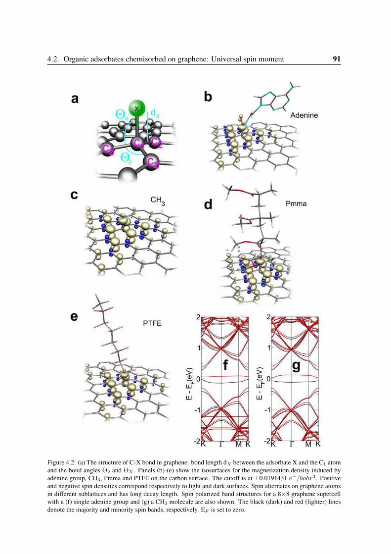
4.2. Organic adsorbates chemisorbed on graphene: Universal spin moment 91
Figure 4.2: (a) The structure of C-X bond in graphene: bond length dX between the adsorbate X and the C1 atomand the bond angles Θ2 and ΘX . Panels (b)-(e) show the isosurfaces for the magnetization density induced byadenine group, CH3, Pmma and PTFE on the carbon surface. The cutoff is at ±0.0191431 e−/bohr3. Positiveand negative spin densities correspond respectively to light and dark surfaces. Spin alternates on graphene atomsin different sublattices and has long decay length. Spin polarized band structures for a 8×8 graphene supercellwith a (f) single adenine group and (g) a CH3 molecule are also shown. The black (dark) and red (lighter) linesdenote the majority and minority spin bands, respectively. EF is set to zero.
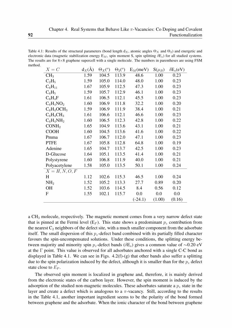
92Chapter 4. Real Systems that Behave Like π-Vacancies: Co Doping and Covalent
Functionalization
Table 4.1: Results of the structural parameters (bond length dX , atomic angles ΘX and Θ2) and energetic andelectronic data (magnetic stabilization energy EM , spin moment S, spin splitting δEs) for all studied systems.The results are for 8×8 graphene supercell with a single molecule. The numbers in parentheses are using FSMmethod.
X = C dX(Å) ΘX(o) Θ2(o) EM (meV) S(µB) δEs(eV)CH3 1.59 104.5 113.9 48.6 1.00 0.23C2H5 1.59 105.0 114.0 48.0 1.00 0.23C6H11 1.67 105.9 112.5 47.3 1.00 0.23C6H5 1.59 105.7 112.9 46.1 1.00 0.23C6H4F 1.61 106.5 112.1 45.5 1.00 0.23C6H4NO2 1.60 106.9 111.8 32.2 1.00 0.20C6H4OCH3 1.59 106.9 111.9 38.4 1.00 0.21C6H4CH3 1.61 106.6 112.1 46.6 1.00 0.23C6H4NH2 1.60 106.5 112.3 42.8 1.00 0.22CONH2 1.65 104.9 113.6 43.1 1.00 0.21COOH 1.60 104.5 113.6 41.6 1.00 0.22Pmma 1.67 106.7 112.0 47.1 1.00 0.23PTFE 1.67 105.8 112.8 64.8 1.00 0.19Adenine 1.65 104.7 113.7 42.5 1.00 0.23D-Glucose 1.64 105.1 113.5 41.4 1.00 0.21Polystyrene 1.60 106.8 111.9 40.0 1.00 0.21Polyacetylene 1.58 105.0 113.5 50.1 1.00 0.24X = H,N,O, FH 1.12 102.6 115.3 46.5 1.00 0.24NH2 1.52 105.2 113.3 27.7 0.89 0.20OH 1.52 103.6 114.5 8.4 0.56 0.12F 1.55 102.1 115.7 0.0 0.0 0.0
(-24.1) (1.00) (0.16)
a CH3 molecule, respectively. The magnetic moment comes from a very narrow defect statethat is pinned at the Fermi level (EF ). This state shows a predominant pz contribution fromthe nearest C2 neighbors of the defect site, with a much smaller component from the adsorbateitself. The small dispersion of this pz-defect band combined with its partially filled characterfavours the spin-uncompensated solutions. Under these conditions, the splitting energy be-tween majority and minority spin pz-defect bands (δEs) gives a common value of ∼0.20 eVat the Γ point. This value is observed for all adsorbates anchored with a single C-C bond asdisplayed in Table 4.1. We can see in Figs. 4.2(f)-(g) that other bands also suffer a splittingdue to the spin polarization induced by the defect, although it is smaller than for the pz defectstate close to EF .
The observed spin moment is localized in graphene and, therefore, it is mainly derivedfrom the electronic states of the carbon layer. However, the spin moment is induced by theadsorption of the studied non-magnetic molecules. These adsorbates saturate a pz state in thelayer and create a defect which is analogous to a π-vacancy. Still, according to the resultsin the Table 4.1, another important ingredient seems to be the polarity of the bond formedbetween graphene and the adsorbate. When the ionic character of the bond between graphene
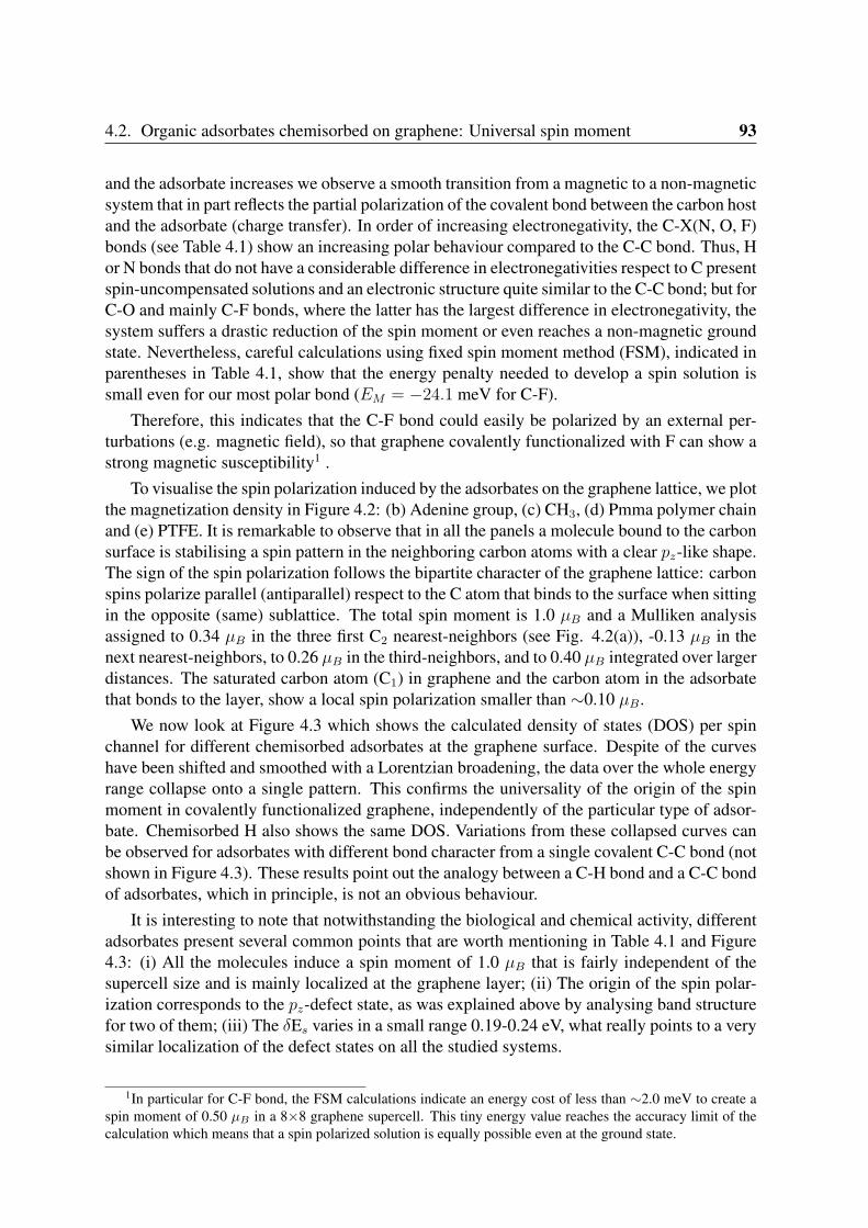
4.2. Organic adsorbates chemisorbed on graphene: Universal spin moment 93
and the adsorbate increases we observe a smooth transition from a magnetic to a non-magneticsystem that in part reflects the partial polarization of the covalent bond between the carbon hostand the adsorbate (charge transfer). In order of increasing electronegativity, the C-X(N, O, F)bonds (see Table 4.1) show an increasing polar behaviour compared to the C-C bond. Thus, Hor N bonds that do not have a considerable difference in electronegativities respect to C presentspin-uncompensated solutions and an electronic structure quite similar to the C-C bond; but forC-O and mainly C-F bonds, where the latter has the largest difference in electronegativity, thesystem suffers a drastic reduction of the spin moment or even reaches a non-magnetic groundstate. Nevertheless, careful calculations using fixed spin moment method (FSM), indicated inparentheses in Table 4.1, show that the energy penalty needed to develop a spin solution issmall even for our most polar bond (EM = −24.1 meV for C-F).
Therefore, this indicates that the C-F bond could easily be polarized by an external per-turbations (e.g. magnetic field), so that graphene covalently functionalized with F can show astrong magnetic susceptibility1 .
To visualise the spin polarization induced by the adsorbates on the graphene lattice, we plotthe magnetization density in Figure 4.2: (b) Adenine group, (c) CH3, (d) Pmma polymer chainand (e) PTFE. It is remarkable to observe that in all the panels a molecule bound to the carbonsurface is stabilising a spin pattern in the neighboring carbon atoms with a clear pz-like shape.The sign of the spin polarization follows the bipartite character of the graphene lattice: carbonspins polarize parallel (antiparallel) respect to the C atom that binds to the surface when sittingin the opposite (same) sublattice. The total spin moment is 1.0 µB and a Mulliken analysisassigned to 0.34 µB in the three first C2 nearest-neighbors (see Fig. 4.2(a)), -0.13 µB in thenext nearest-neighbors, to 0.26 µB in the third-neighbors, and to 0.40 µB integrated over largerdistances. The saturated carbon atom (C1) in graphene and the carbon atom in the adsorbatethat bonds to the layer, show a local spin polarization smaller than ∼0.10 µB.
We now look at Figure 4.3 which shows the calculated density of states (DOS) per spinchannel for different chemisorbed adsorbates at the graphene surface. Despite of the curveshave been shifted and smoothed with a Lorentzian broadening, the data over the whole energyrange collapse onto a single pattern. This confirms the universality of the origin of the spinmoment in covalently functionalized graphene, independently of the particular type of adsor-bate. Chemisorbed H also shows the same DOS. Variations from these collapsed curves canbe observed for adsorbates with different bond character from a single covalent C-C bond (notshown in Figure 4.3). These results point out the analogy between a C-H bond and a C-C bondof adsorbates, which in principle, is not an obvious behaviour.
It is interesting to note that notwithstanding the biological and chemical activity, differentadsorbates present several common points that are worth mentioning in Table 4.1 and Figure4.3: (i) All the molecules induce a spin moment of 1.0 µB that is fairly independent of thesupercell size and is mainly localized at the graphene layer; (ii) The origin of the spin polar-ization corresponds to the pz-defect state, as was explained above by analysing band structurefor two of them; (iii) The δEs varies in a small range 0.19-0.24 eV, what really points to a verysimilar localization of the defect states on all the studied systems.
1In particular for C-F bond, the FSM calculations indicate an energy cost of less than ∼2.0 meV to create aspin moment of 0.50 µB in a 8×8 graphene supercell. This tiny energy value reaches the accuracy limit of thecalculation which means that a spin polarized solution is equally possible even at the ground state.
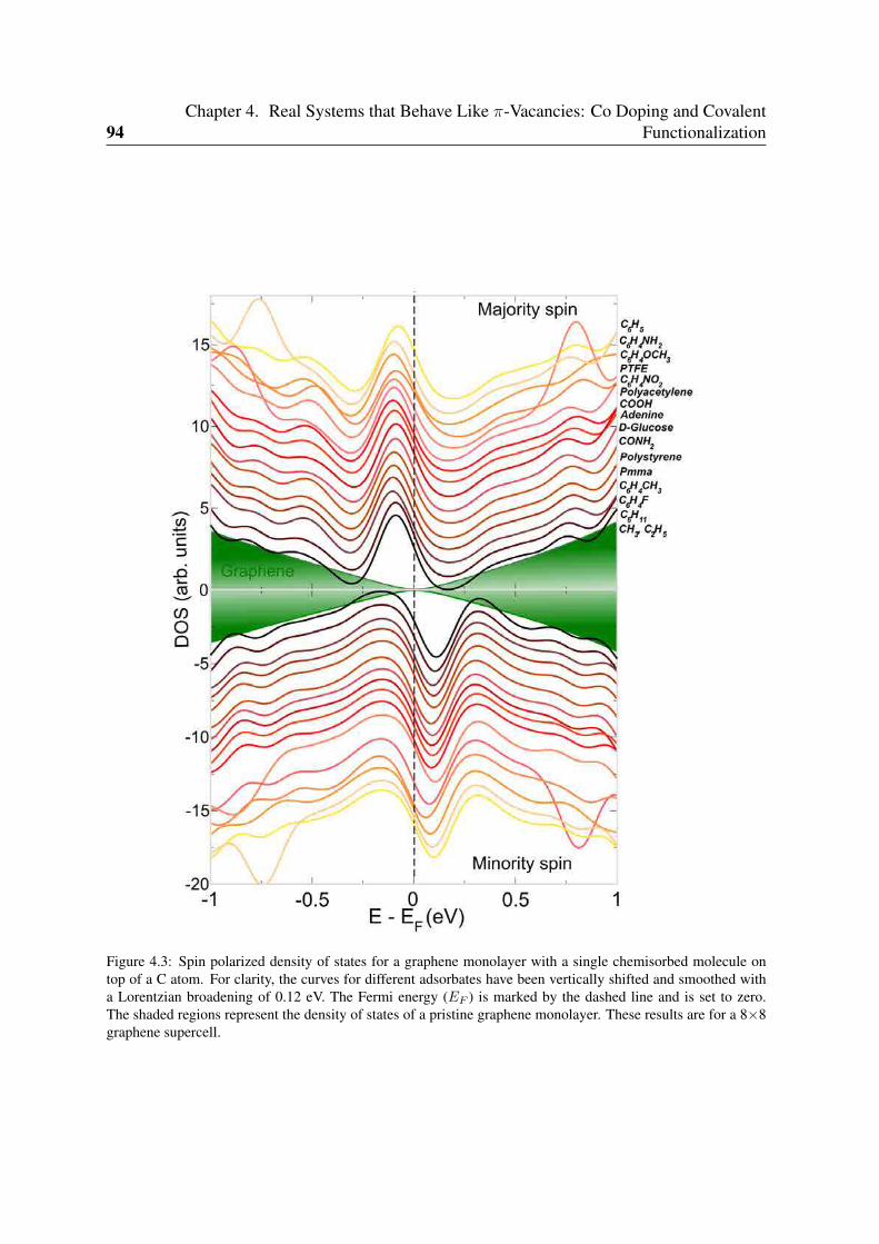
94Chapter 4. Real Systems that Behave Like π-Vacancies: Co Doping and Covalent
Functionalization
Figure 4.3: Spin polarized density of states for a graphene monolayer with a single chemisorbed molecule ontop of a C atom. For clarity, the curves for different adsorbates have been vertically shifted and smoothed witha Lorentzian broadening of 0.12 eV. The Fermi energy (EF ) is marked by the dashed line and is set to zero.The shaded regions represent the density of states of a pristine graphene monolayer. These results are for a 8×8graphene supercell.
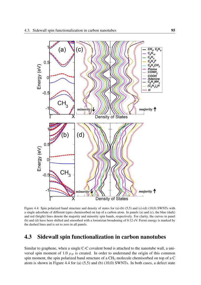
4.3. Sidewall spin functionalization in carbon nanotubes 95
Figure 4.4: Spin polarized band structure and density of states for (a)-(b) (5,5) and (c)-(d) (10,0) SWNTs witha single adsorbate of different types chemisorbed on top of a carbon atom. In panels (a) and (c), the blue (dark)and red (bright) lines denote the majority and minority spin bands, respectively. For clarity, the curves in panel(b) and (d) have been shifted and smoothed with a lorentzian broadening of 0.12 eV. Fermi energy is marked bythe dashed lines and is set to zero in all panels.
4.3 Sidewall spin functionalization in carbon nanotubes
Similar to graphene, when a single C-C covalent bond is attached to the nanotube wall, a uni-versal spin moment of 1.0 µB is created. In order to understand the origin of this commonspin moment, the spin polarized band structure of a CH3 molecule chemisorbed on top of a Catom is shown in Figure 4.4 for (a) (5,5) and (b) (10,0) SWNTs. In both cases, a defect state
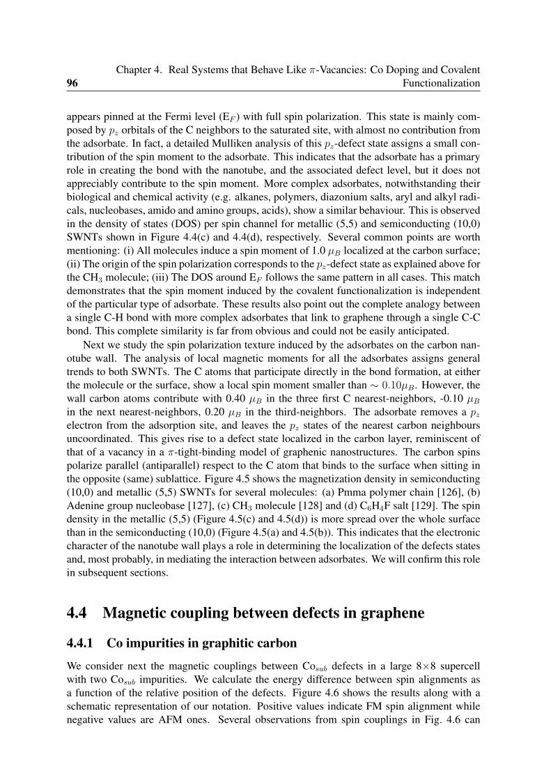
96Chapter 4. Real Systems that Behave Like π-Vacancies: Co Doping and Covalent
Functionalization
appears pinned at the Fermi level (EF ) with full spin polarization. This state is mainly com-posed by pz orbitals of the C neighbors to the saturated site, with almost no contribution fromthe adsorbate. In fact, a detailed Mulliken analysis of this pz-defect state assigns a small con-tribution of the spin moment to the adsorbate. This indicates that the adsorbate has a primaryrole in creating the bond with the nanotube, and the associated defect level, but it does notappreciably contribute to the spin moment. More complex adsorbates, notwithstanding theirbiological and chemical activity (e.g. alkanes, polymers, diazonium salts, aryl and alkyl radi-cals, nucleobases, amido and amino groups, acids), show a similar behaviour. This is observedin the density of states (DOS) per spin channel for metallic (5,5) and semiconducting (10,0)SWNTs shown in Figure 4.4(c) and 4.4(d), respectively. Several common points are worthmentioning: (i) All molecules induce a spin moment of 1.0 µB localized at the carbon surface;(ii) The origin of the spin polarization corresponds to the pz-defect state as explained above forthe CH3 molecule; (iii) The DOS around EF follows the same pattern in all cases. This matchdemonstrates that the spin moment induced by the covalent functionalization is independentof the particular type of adsorbate. These results also point out the complete analogy betweena single C-H bond with more complex adsorbates that link to graphene through a single C-Cbond. This complete similarity is far from obvious and could not be easily anticipated.
Next we study the spin polarization texture induced by the adsorbates on the carbon nan-otube wall. The analysis of local magnetic moments for all the adsorbates assigns generaltrends to both SWNTs. The C atoms that participate directly in the bond formation, at eitherthe molecule or the surface, show a local spin moment smaller than ∼ 0.10µB. However, thewall carbon atoms contribute with 0.40 µB in the three first C nearest-neighbors, -0.10 µB
in the next nearest-neighbors, 0.20 µB in the third-neighbors. The adsorbate removes a pz
electron from the adsorption site, and leaves the pz states of the nearest carbon neighboursuncoordinated. This gives rise to a defect state localized in the carbon layer, reminiscent ofthat of a vacancy in a π-tight-binding model of graphenic nanostructures. The carbon spinspolarize parallel (antiparallel) respect to the C atom that binds to the surface when sitting inthe opposite (same) sublattice. Figure 4.5 shows the magnetization density in semiconducting(10,0) and metallic (5,5) SWNTs for several molecules: (a) Pmma polymer chain [126], (b)Adenine group nucleobase [127], (c) CH3 molecule [128] and (d) C6H4F salt [129]. The spindensity in the metallic (5,5) (Figure 4.5(c) and 4.5(d)) is more spread over the whole surfacethan in the semiconducting (10,0) (Figure 4.5(a) and 4.5(b)). This indicates that the electroniccharacter of the nanotube wall plays a role in determining the localization of the defects statesand, most probably, in mediating the interaction between adsorbates. We will confirm this rolein subsequent sections.
4.4 Magnetic coupling between defects in graphene
4.4.1 Co impurities in graphitic carbon
We consider next the magnetic couplings between Cosub defects in a large 8×8 supercellwith two Cosub impurities. We calculate the energy difference between spin alignments asa function of the relative position of the defects. Figure 4.6 shows the results along with aschematic representation of our notation. Positive values indicate FM spin alignment whilenegative values are AFM ones. Several observations from spin couplings in Fig. 4.6 can
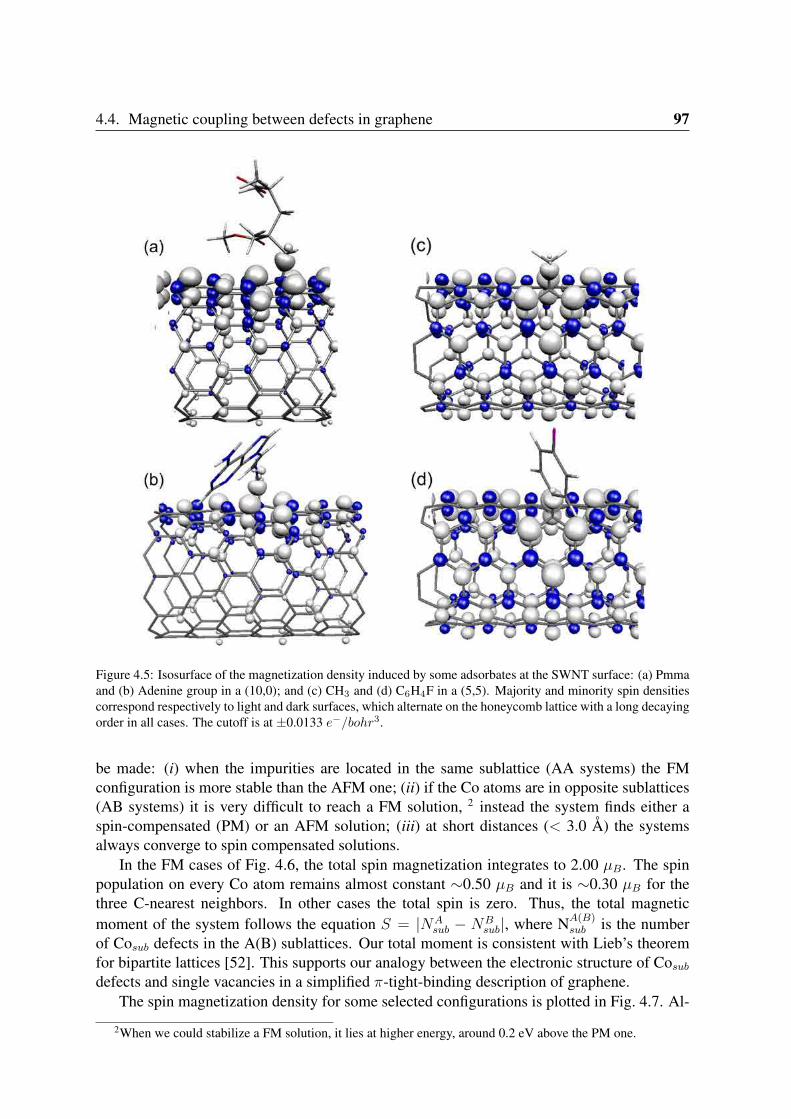
4.4. Magnetic coupling between defects in graphene 97
Figure 4.5: Isosurface of the magnetization density induced by some adsorbates at the SWNT surface: (a) Pmmaand (b) Adenine group in a (10,0); and (c) CH3 and (d) C6H4F in a (5,5). Majority and minority spin densitiescorrespond respectively to light and dark surfaces, which alternate on the honeycomb lattice with a long decayingorder in all cases. The cutoff is at ±0.0133 e−/bohr3.
be made: (i) when the impurities are located in the same sublattice (AA systems) the FMconfiguration is more stable than the AFM one; (ii) if the Co atoms are in opposite sublattices(AB systems) it is very difficult to reach a FM solution, 2 instead the system finds either aspin-compensated (PM) or an AFM solution; (iii) at short distances (< 3.0 Å) the systemsalways converge to spin compensated solutions.
In the FM cases of Fig. 4.6, the total spin magnetization integrates to 2.00 µB. The spinpopulation on every Co atom remains almost constant ∼0.50 µB and it is ∼0.30 µB for thethree C-nearest neighbors. In other cases the total spin is zero. Thus, the total magneticmoment of the system follows the equation S = |NA
sub − NBsub|, where NA(B)
sub is the numberof Cosub defects in the A(B) sublattices. Our total moment is consistent with Lieb’s theoremfor bipartite lattices [52]. This supports our analogy between the electronic structure of Cosub
defects and single vacancies in a simplified π-tight-binding description of graphene.The spin magnetization density for some selected configurations is plotted in Fig. 4.7. Al-
2When we could stabilize a FM solution, it lies at higher energy, around 0.2 eV above the PM one.
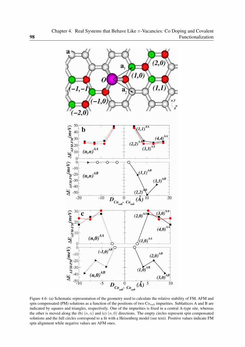
98Chapter 4. Real Systems that Behave Like π-Vacancies: Co Doping and Covalent
Functionalization
Figure 4.6: (a) Schematic representation of the geometry used to calculate the relative stability of FM, AFM andspin compensated (PM) solutions as a function of the positions of two Cosub impurities. Sublattices A and B areindicated by squares and triangles, respectively. One of the impurities is fixed in a central A-type site, whereasthe other is moved along the (b) (n, n) and (c) (n, 0) directions. The empty circles represent spin compensatedsolutions and the full circles correspond to a fit with a Heisenberg model (see text). Positive values indicate FMspin alignment while negative values are AFM ones.
4.4. Magnetic coupling between defects in graphene 99
a
b
c(−4,−4)
(2,2)
(1,1)AA
AB
AB
Figure 4.7: (a) Spin densities for configurations (a) (1, 1)AA, (b) (2, 2)AB and (c) (−4,−4)AB(see Fig. 4.6(a) forthe nomenclature). Positive and negative spin densities are indicated by light (gray) and dark (blue) isosurfacescorresponding to ±0.001 e−/Bohr3, respectively.
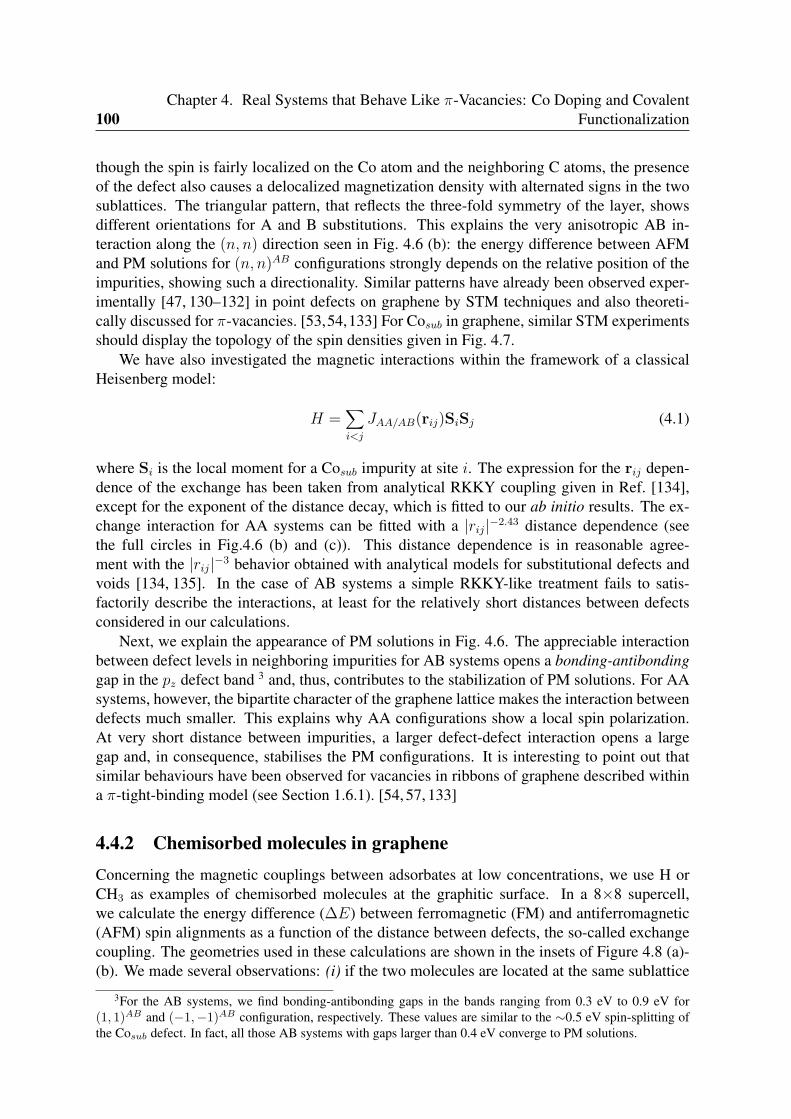
100Chapter 4. Real Systems that Behave Like π-Vacancies: Co Doping and Covalent
Functionalization
though the spin is fairly localized on the Co atom and the neighboring C atoms, the presenceof the defect also causes a delocalized magnetization density with alternated signs in the twosublattices. The triangular pattern, that reflects the three-fold symmetry of the layer, showsdifferent orientations for A and B substitutions. This explains the very anisotropic AB in-teraction along the (n, n) direction seen in Fig. 4.6 (b): the energy difference between AFMand PM solutions for (n, n)AB configurations strongly depends on the relative position of theimpurities, showing such a directionality. Similar patterns have already been observed exper-imentally [47, 130–132] in point defects on graphene by STM techniques and also theoreti-cally discussed for π-vacancies. [53,54,133] For Cosub in graphene, similar STM experimentsshould display the topology of the spin densities given in Fig. 4.7.
We have also investigated the magnetic interactions within the framework of a classicalHeisenberg model:
H =∑i<j
JAA/AB(rij)SiSj (4.1)
where Si is the local moment for a Cosub impurity at site i. The expression for the rij depen-dence of the exchange has been taken from analytical RKKY coupling given in Ref. [134],except for the exponent of the distance decay, which is fitted to our ab initio results. The ex-change interaction for AA systems can be fitted with a |rij|−2.43 distance dependence (seethe full circles in Fig.4.6 (b) and (c)). This distance dependence is in reasonable agree-ment with the |rij|−3 behavior obtained with analytical models for substitutional defects andvoids [134, 135]. In the case of AB systems a simple RKKY-like treatment fails to satis-factorily describe the interactions, at least for the relatively short distances between defectsconsidered in our calculations.
Next, we explain the appearance of PM solutions in Fig. 4.6. The appreciable interactionbetween defect levels in neighboring impurities for AB systems opens a bonding-antibondinggap in the pz defect band 3 and, thus, contributes to the stabilization of PM solutions. For AAsystems, however, the bipartite character of the graphene lattice makes the interaction betweendefects much smaller. This explains why AA configurations show a local spin polarization.At very short distance between impurities, a larger defect-defect interaction opens a largegap and, in consequence, stabilises the PM configurations. It is interesting to point out thatsimilar behaviours have been observed for vacancies in ribbons of graphene described withina π-tight-binding model (see Section 1.6.1). [54, 57, 133]
4.4.2 Chemisorbed molecules in grapheneConcerning the magnetic couplings between adsorbates at low concentrations, we use H orCH3 as examples of chemisorbed molecules at the graphitic surface. In a 8×8 supercell,we calculate the energy difference (∆E) between ferromagnetic (FM) and antiferromagnetic(AFM) spin alignments as a function of the distance between defects, the so-called exchangecoupling. The geometries used in these calculations are shown in the insets of Figure 4.8 (a)-(b). We made several observations: (i) if the two molecules are located at the same sublattice
3For the AB systems, we find bonding-antibonding gaps in the bands ranging from 0.3 eV to 0.9 eV for(1, 1)AB and (−1,−1)AB configuration, respectively. These values are similar to the ∼0.5 eV spin-splitting ofthe Cosub defect. In fact, all those AB systems with gaps larger than 0.4 eV converge to PM solutions.
4.4. Magnetic coupling between defects in graphene 101
Figure 4.8: Exchange coupling as a function of the position for two adsorbates, H and CH3, chemisorbed on topof a C atom in a 8×8 graphene supercell. One of the molecules is moved along the (a) armchair and (b) zigzagdirections and the other remains at the origin. The filled and empty squares correspond, respectively, to H andCH3 at the same sublattice (AA) and the triangles correspond to both adsorbates at different sublattices (AB).The circles correspond to the best fit to a Heisenberg model for the AA sites.
(AA), the FM configuration is most stable than the AFM one. In the FM case, the total spinmagnetization integrates to 2.00 µB for both H and CH3, with a local spin population thatremains nearly constant at every defect site; (ii) if both molecules are located at differentsublattices (AB), we could not stabilize any magnetic solution, and the system converge to aspin compensated solution with no local moment; (iii) at short distances (< 5.0 Å) the systemwith chemisorbed CH3 molecules converges to FM solutions, while it was not possible tostabilize any AFM spin order.
The above magnetic behaviour for adsorbates at different sublattices can be rationalisedas follows. When the molecules are located at opposite sublattice the interaction betweendefect levels in neighboring adsorbates is appreciable. Similar to what we have already seenfor Cosub impurities, and in close analogy to the behaviour observed for π-vacancies [54], thisinteraction opens a bonding-antibonding gap in the pz defect bands which contributes to thestabilization of spin compensated solutions. If the gap is larger than the splitting δEs of themajority and minority spin defect bands around EF the system will be non-magnetic [115]. Adetailed analysis of the band structure for both adsorbates fully confirms this interpretation. Itis noteworth that a similar behavior was also observed for hydrogen [136] and vacancies [57].All of them have thus an electronic structure similar to that of H in graphene, which in turn is
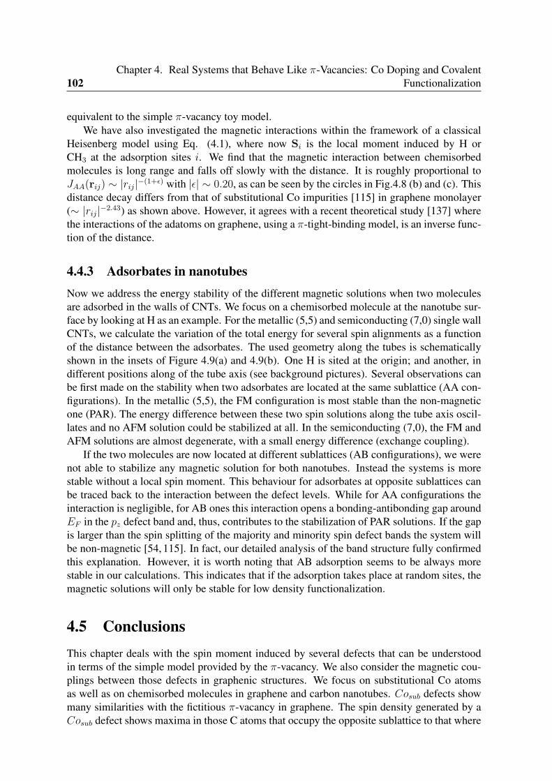
102Chapter 4. Real Systems that Behave Like π-Vacancies: Co Doping and Covalent
Functionalization
equivalent to the simple π-vacancy toy model.We have also investigated the magnetic interactions within the framework of a classical
Heisenberg model using Eq. (4.1), where now Si is the local moment induced by H orCH3 at the adsorption sites i. We find that the magnetic interaction between chemisorbedmolecules is long range and falls off slowly with the distance. It is roughly proportional toJAA(rij) ∼ |rij|−(1+ϵ) with |ϵ| ∼ 0.20, as can be seen by the circles in Fig.4.8 (b) and (c). Thisdistance decay differs from that of substitutional Co impurities [115] in graphene monolayer(∼ |rij|−2.43) as shown above. However, it agrees with a recent theoretical study [137] wherethe interactions of the adatoms on graphene, using a π-tight-binding model, is an inverse func-tion of the distance.
4.4.3 Adsorbates in nanotubesNow we address the energy stability of the different magnetic solutions when two moleculesare adsorbed in the walls of CNTs. We focus on a chemisorbed molecule at the nanotube sur-face by looking at H as an example. For the metallic (5,5) and semiconducting (7,0) single wallCNTs, we calculate the variation of the total energy for several spin alignments as a functionof the distance between the adsorbates. The used geometry along the tubes is schematicallyshown in the insets of Figure 4.9(a) and 4.9(b). One H is sited at the origin; and another, indifferent positions along of the tube axis (see background pictures). Several observations canbe first made on the stability when two adsorbates are located at the same sublattice (AA con-figurations). In the metallic (5,5), the FM configuration is most stable than the non-magneticone (PAR). The energy difference between these two spin solutions along the tube axis oscil-lates and no AFM solution could be stabilized at all. In the semiconducting (7,0), the FM andAFM solutions are almost degenerate, with a small energy difference (exchange coupling).
If the two molecules are now located at different sublattices (AB configurations), we werenot able to stabilize any magnetic solution for both nanotubes. Instead the systems is morestable without a local spin moment. This behaviour for adsorbates at opposite sublattices canbe traced back to the interaction between the defect levels. While for AA configurations theinteraction is negligible, for AB ones this interaction opens a bonding-antibonding gap aroundEF in the pz defect band and, thus, contributes to the stabilization of PAR solutions. If the gapis larger than the spin splitting of the majority and minority spin defect bands the system willbe non-magnetic [54, 115]. In fact, our detailed analysis of the band structure fully confirmedthis explanation. However, it is worth noting that AB adsorption seems to be always morestable in our calculations. This indicates that if the adsorption takes place at random sites, themagnetic solutions will only be stable for low density functionalization.
4.5 ConclusionsThis chapter deals with the spin moment induced by several defects that can be understoodin terms of the simple model provided by the π-vacancy. We also consider the magnetic cou-plings between those defects in graphenic structures. We focus on substitutional Co atomsas well as on chemisorbed molecules in graphene and carbon nanotubes. Cosub defects showmany similarities with the fictitious π-vacancy in graphene. The spin density generated by aCosub defect shows maxima in those C atoms that occupy the opposite sublattice to that where
4.5. Conclusions 103
Figure 4.9: Variation of total energy with the H positions for the distinct magnetic solutions in the two graphiticsublattices (AA and AB). One of the molecules is moved along the axis of a (a) (5,5) and a (b) (7,0) SWNT; and,the other remaining at the origin (see background pictures). The empty and filled squares correspond to PAR spinsolutions at AB and AA sublattices, respectively. The circles and triangles indicate the FM and AFM solutions,respectively, at the same sublattice.
Co sites, following the bipartite character of the graphene lattice. For two Co substitutionals,we distinguish between AA and AB positions. For AA cases, the induced moments align fer-romagnetically and the strength of the couplings depends on the relative distance as |rij|−2.43.The total moment follows Lieb’s theorem similarly to a collection of π-vacancies. For ABcases, the band structures around Fermi energy show the opening of antibonding-bondinggaps between defect levels in neighboring defect sites, which suggests large interactions be-tween them. The alignments of the magnetic moments are AFM or PM, a trend that is alsosimilar to that found for π-vacancies [54, 57, 133]. To end this part we ought to remark thatthe origin of the spin moments and the sign of the couplings stem from the bipartite lattice ofgraphene.
The analysis of the magnetic properties induced by chemisorbed molecules in grapheneand carbon nanotubes was conducted using many types of adsorbates: polymers, diazoniumsalts, aryl and alkyl radicals, nucleobases, amide and amine groups, sugar, organic acids. Aspin moment of 1.00 µB is induced at the carbon surface always that a single C-C bond isformed between an adsorbate and the graphenic layer. This moment was observed to be in-dependent of the supercell size, and it is stabilized by several tenths of meV respect to thenon-magnetic phase. AA adsorption always leads to FM alignment. AB adsorption, how-ever, always stabilises non-magnetic solutions. The global spin moment follows again theLieb’s theorem. Similarly to Co impurities, a RKKY-like model was used to fit the calculated

104Chapter 4. Real Systems that Behave Like π-Vacancies: Co Doping and Covalent
Functionalization
magnetic interactions. The interactions decay slowly in the bipartite lattice, being roughlyproportional to the inverse of distance.
Metallic carbon nanotubes behave similarly to graphene. For molecules chemisorbed atthe same sublattice (AA adsorption) we could only stabilize FM or PM configurations. TheFM solutions are more stable than the PM ones. In semiconducting nanotubes, FM and AFMsolutions are almost degenerate even for AA adsorption, with a small energy difference alongthe tube axis. For two molecules in different sublattices (AB adsorption), we could not stabi-lize any magnetic solution and the system is more stable without a local spin moment.
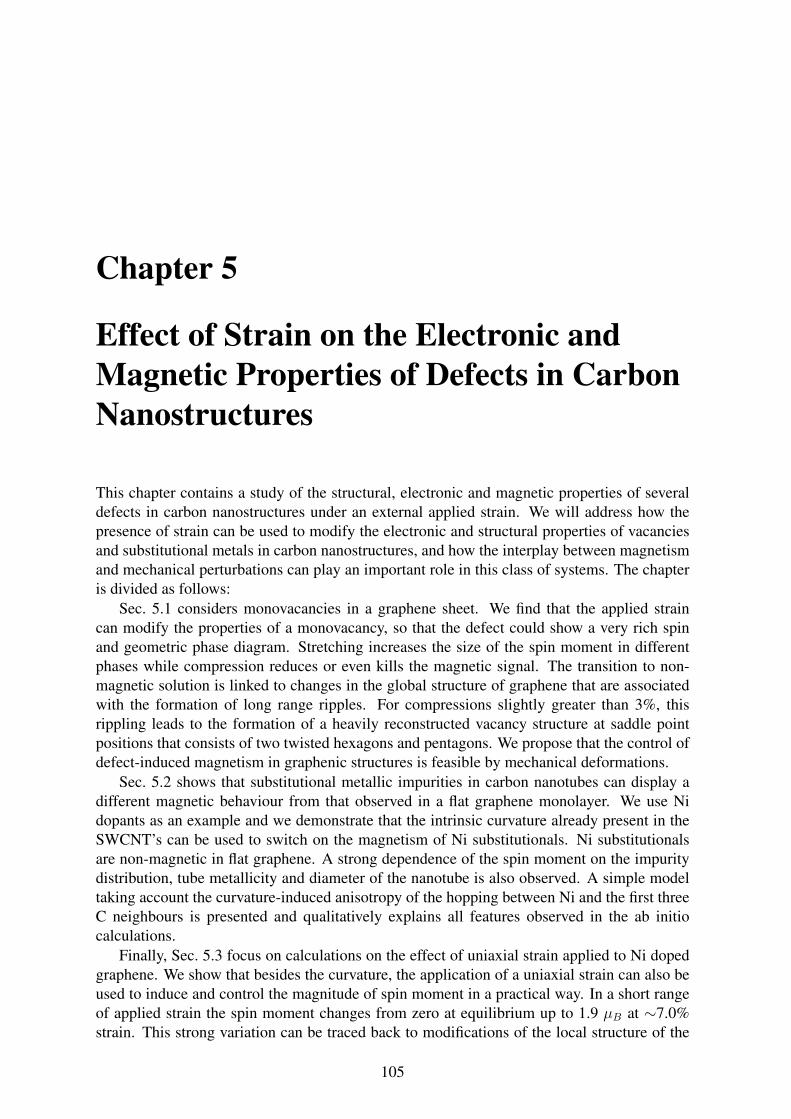
Chapter 5
Effect of Strain on the Electronic andMagnetic Properties of Defects in CarbonNanostructures
This chapter contains a study of the structural, electronic and magnetic properties of severaldefects in carbon nanostructures under an external applied strain. We will address how thepresence of strain can be used to modify the electronic and structural properties of vacanciesand substitutional metals in carbon nanostructures, and how the interplay between magnetismand mechanical perturbations can play an important role in this class of systems. The chapteris divided as follows:
Sec. 5.1 considers monovacancies in a graphene sheet. We find that the applied straincan modify the properties of a monovacancy, so that the defect could show a very rich spinand geometric phase diagram. Stretching increases the size of the spin moment in differentphases while compression reduces or even kills the magnetic signal. The transition to non-magnetic solution is linked to changes in the global structure of graphene that are associatedwith the formation of long range ripples. For compressions slightly greater than 3%, thisrippling leads to the formation of a heavily reconstructed vacancy structure at saddle pointpositions that consists of two twisted hexagons and pentagons. We propose that the control ofdefect-induced magnetism in graphenic structures is feasible by mechanical deformations.
Sec. 5.2 shows that substitutional metallic impurities in carbon nanotubes can display adifferent magnetic behaviour from that observed in a flat graphene monolayer. We use Nidopants as an example and we demonstrate that the intrinsic curvature already present in theSWCNT’s can be used to switch on the magnetism of Ni substitutionals. Ni substitutionalsare non-magnetic in flat graphene. A strong dependence of the spin moment on the impuritydistribution, tube metallicity and diameter of the nanotube is also observed. A simple modeltaking account the curvature-induced anisotropy of the hopping between Ni and the first threeC neighbours is presented and qualitatively explains all features observed in the ab initiocalculations.
Finally, Sec. 5.3 focus on calculations on the effect of uniaxial strain applied to Ni dopedgraphene. We show that besides the curvature, the application of a uniaxial strain can also beused to induce and control the magnitude of spin moment in a practical way. In a short rangeof applied strain the spin moment changes from zero at equilibrium up to 1.9 µB at ∼7.0%strain. This strong variation can be traced back to modifications of the local structure of the
105
106Chapter 5. Effect of Strain on the Electronic and Magnetic Properties of Defects in Carbon
Nanostructures
defect. These structural changes can be related to those of the unreconstructed carbon vacancyin graphene under strain which presents strong similarities with Ni substitutionals impurities.
The chapter ends with the conclusions in Sec. 5.4.
5.1 A general spin-strain phase diagram for a monovacancyin graphene
In this section we study the effect of isotropic strain on the electronic structure of vacanciesin graphene. The interplay between global and local structures reflects directly in the simul-taneous observation of new types of spin solutions, defect reconstruction and corrugation onthe whole system. The 2D-character of graphene combined with its intrinsic rippled geometryprovide the necessary framework for this new kind of effects. We focus on carbon monova-cancy, and find that it shows a rich structural and spin phase diagram as a function of strain.
5.1.1 Structure versus strain
We start taking a look at Figure 5.1 which illustrates the relaxed geometry of one of our mod-els of a free-standing defective graphene layer under a 1.2 % isotropic compression. Whileunder tension the layer remains perfectly flat, and small compression produces the sponta-neous rippling of graphene with a characteristic deformation around the vacancy. At zerostrain, the monovacancy tends to undergo a Jahn-Teller–like distortion that lowers its energyby ∼200 meV: atoms of type 1 (see the inset of Fig. 5.1) reconstruct to form a pentagon withthe neighboring atoms, while atom 2 is left with the dangling bond responsible for the spinpolarization. Although we herein consider a non-planar structure under strain, our findingsat low compressions are similar to results previously obtained for flat graphene [42, 121].However, atom 2 in our rippled structure is progressively lifted from the graphene surface byas much as ∼1.0 Å for strains slightly below 3%, just before the occurrence of a strong va-cancy reconstruction. The data of Figure 5.1B reveal a particularly striking result. In contrastto 2D vacancy, for which previous authors invariably described a ’pentagon-goggles’ struc-ture, our own calculations show that the vacancy is strongly reconstructed under rippling. Forcompressive strains greater than 3%, an altogether new defect structure is produced consistingof two heavily distorted hexagons and pentagons and resembling the transition states for themovement of a planar monovacancy. We shall now focus on the description of this region oftransition for compression of up to 2.8%.
Figure 5.2A shows the maximum amplitude of the rippling h as a function of strain fordefective graphene (shown by the solid symbols). We removed the defects from each rip-pled structure by adding carbon atoms to the vacancy sites and relaxing the structure. Weobtained rippled pristine graphene with maximum amplitudes as shown in Figure 5.2A (opensymbols). The amplitudes and the topographic patterns (insets in Figure 5.2A) show littledifference between pristine or defective graphene, particularly for compressive strains greaterthan ∼1%. It seems that even for large supercells, the main determinant to observe ripples isthe applied strain. However, the structural patterns that occurs in defective graphene define apreferential direction and break the up-down symmetry that exits perpendicular to the layer.This preferential direction and the symmetry breaking are explained by the presence of the
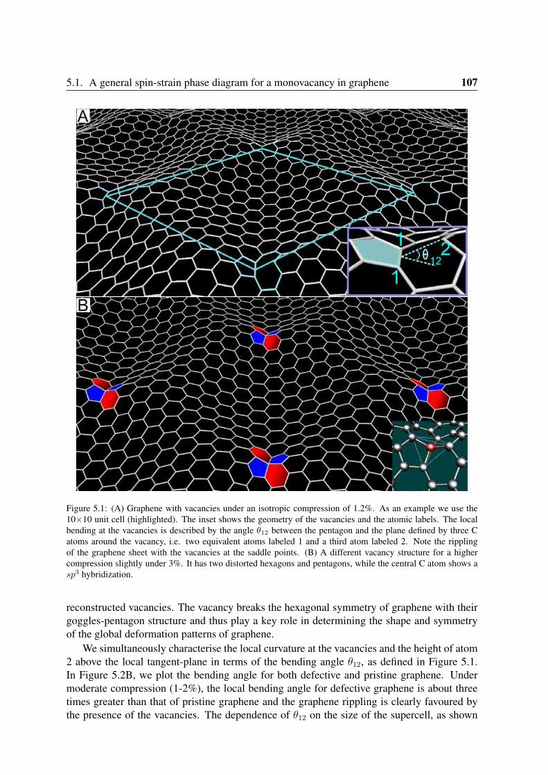
5.1. A general spin-strain phase diagram for a monovacancy in graphene 107
Figure 5.1: (A) Graphene with vacancies under an isotropic compression of 1.2%. As an example we use the10×10 unit cell (highlighted). The inset shows the geometry of the vacancies and the atomic labels. The localbending at the vacancies is described by the angle θ12 between the pentagon and the plane defined by three Catoms around the vacancy, i.e. two equivalent atoms labeled 1 and a third atom labeled 2. Note the ripplingof the graphene sheet with the vacancies at the saddle points. (B) A different vacancy structure for a highercompression slightly under 3%. It has two distorted hexagons and pentagons, while the central C atom shows asp3 hybridization.
reconstructed vacancies. The vacancy breaks the hexagonal symmetry of graphene with theirgoggles-pentagon structure and thus play a key role in determining the shape and symmetryof the global deformation patterns of graphene.
We simultaneously characterise the local curvature at the vacancies and the height of atom2 above the local tangent-plane in terms of the bending angle θ12, as defined in Figure 5.1.In Figure 5.2B, we plot the bending angle for both defective and pristine graphene. Undermoderate compression (1-2%), the local bending angle for defective graphene is about threetimes greater than that of pristine graphene and the graphene rippling is clearly favoured bythe presence of the vacancies. The dependence of θ12 on the size of the supercell, as shown
108Chapter 5. Effect of Strain on the Electronic and Magnetic Properties of Defects in Carbon
Nanostructures
Figure 5.2: (A) Maximum amplitude h(Å) of rippling for 10×10 graphene supercells versus strain in units of theequilibrium lattice constant ao. The filled circles denote defective graphene, while the empty circles denote thepristine layer that has been recovered by adding a carbon atom to the vacancy. The insets show the corrugationpatterns: the bright/yellow (dark/green) areas indicate the higher (lower) regions. (B) Bending angle θ12 (seedefinition in Figure 5.1) as a function of strain. The inset shows the behavior of the bending angles with sizeof supercell for different values of strain. The local induced deformation clearly depends on the presence ofvacancies and on the size of the supercell.
in the inset of Fig.5.2B, further demonstrates the coupling between the local geometry of thedefect and the global deformation. For example, for a 4 × 4 supercell, a strain larger than1.0% is required to obtain an increase in θ12 and to allow the corrugation of the layer to begin.However, for larger supercells, much smaller strains cause appreciable deformations aroundthe vacancies.
5.1.2 EnergeticsIt is worth mentioning that the range of applied strain used here (a few percent) is comparableto that present in experiments in which an appreciable corrugation of graphene was reportedfor supported layers [138–140], chemically functionalized graphene [141] , or defective lay-ers [142]. As a result of the imposed periodicity and the finite-sizes used in our calculations,long-wavelength deformations appear primarily to be related to the strain, i.e. vacancies donot create significant corrugation in the relaxed geometry at the equilibrium lattice constant.However, we observe that for the range of strain considered here, the system is compressedand thereby assumes a rippled configuration at an energy between two and three times lowerfor defective graphene than for the pristine layer. For a 10x10 supercell, the energy requiredto create ripples for a compression of 3% is reduced to almost half its value in the presenceof vacancies, as seen in Figure 5.3A. This difference in energy is consistent with the proposedrole of vacancies as a source of ripples in recent experiments [142].
5.1.3 Magnetism versus strain: several spin solutionsEarlier we commented on the fact that isotropic strain can be used to tune the vacancy structureand the curvature of the layer at the site of the defect. We now focus on the influence of these

5.1. A general spin-strain phase diagram for a monovacancy in graphene 109
Figure 5.3: Variation in total energy per atom (A), spin moment (B), and bond length (C) versus strain for threedifferent configurations of vacancy in the 10×10 supercell: high-spin flat (triangles), low-spin flat (squares)and low-spin rippled (circles). The inset in panel (a) details the change in total energy with respect to thelow-spin solutions at about zero strain. The filled and empty symbols in panel (C) represent the 1-2 and 1-1distances, respectively (see the inset of Figure 5.1 for atomic labels). The marks given by stars refer to theaverage distances as the geometry departs from the usual vacancy to the structure in Figure 5.1B. Note that themagnetism disappears at a strain of ∼2% when allowing for out-of-plane deformations.
structural changes on the magnetic and electronic properties of the vacancies. We first considerthe case of zero strain, i.e. at the equilibrium lattice constant. The usual reconstruction [42,121] is accompanied by a decrease in the 1-1 distance in Figure 5.1 and an increase in the1-2 distances. The two dangling bonds in the type 1 atoms are thus saturated while atom 2remains uncoordinated. It is the polarization of the corresponding dangling bond that is themain reason behind the appearance of a spin moment of ∼1.5µB associated with the carbonmonovacancy. However, we were able to stabilize another reconstruction characterized bya different structural distortion, in which the 1-2 distance decreases, while the 1-1 distanceincreases [see the local structures and distances in Fig.5.3B,C]. This structure has a larger spinmoment of ∼1.82µB. We refer to this latter structure as the high-spin (HS) configuration, andto the former as the low-spin (LS) configuration. At zero strain the LS structure is more stablethan the HS by around 250 meV.
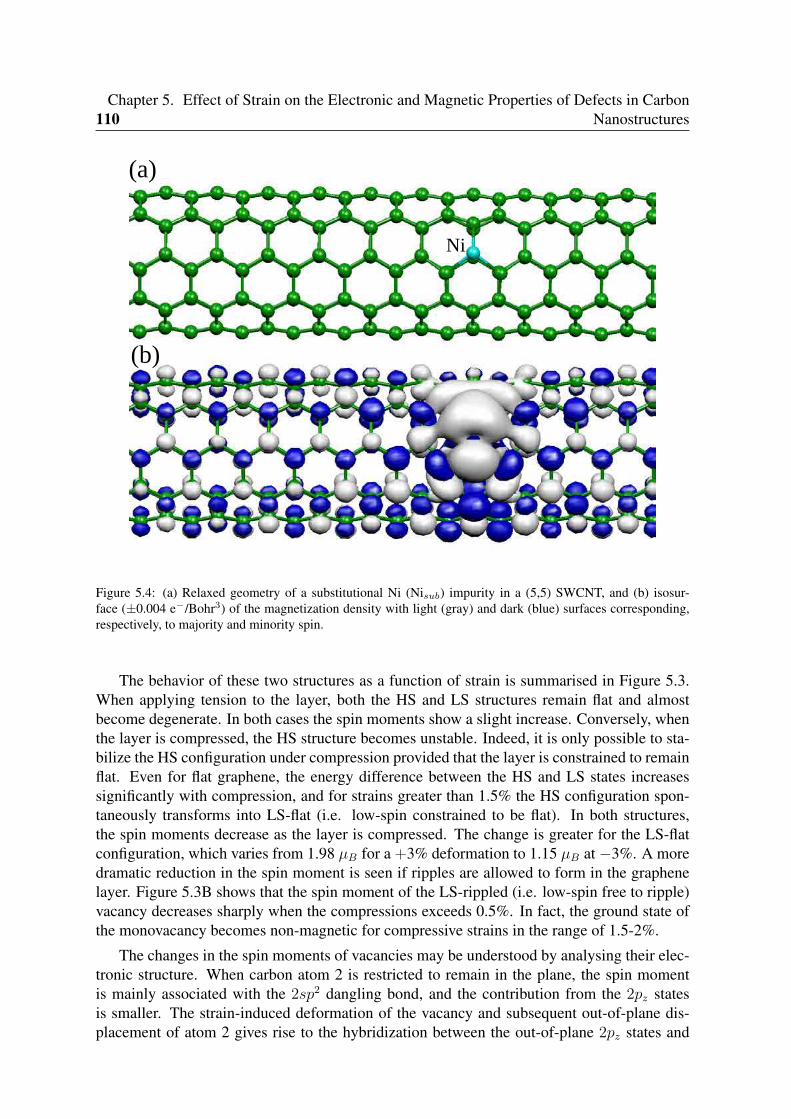
110Chapter 5. Effect of Strain on the Electronic and Magnetic Properties of Defects in Carbon
Nanostructures
(a)
(b)
Ni
Figure 5.4: (a) Relaxed geometry of a substitutional Ni (Nisub) impurity in a (5,5) SWCNT, and (b) isosur-face (±0.004 e−/Bohr3) of the magnetization density with light (gray) and dark (blue) surfaces corresponding,respectively, to majority and minority spin.
The behavior of these two structures as a function of strain is summarised in Figure 5.3.When applying tension to the layer, both the HS and LS structures remain flat and almostbecome degenerate. In both cases the spin moments show a slight increase. Conversely, whenthe layer is compressed, the HS structure becomes unstable. Indeed, it is only possible to sta-bilize the HS configuration under compression provided that the layer is constrained to remainflat. Even for flat graphene, the energy difference between the HS and LS states increasessignificantly with compression, and for strains greater than 1.5% the HS configuration spon-taneously transforms into LS-flat (i.e. low-spin constrained to be flat). In both structures,the spin moments decrease as the layer is compressed. The change is greater for the LS-flatconfiguration, which varies from 1.98 µB for a +3% deformation to 1.15 µB at −3%. A moredramatic reduction in the spin moment is seen if ripples are allowed to form in the graphenelayer. Figure 5.3B shows that the spin moment of the LS-rippled (i.e. low-spin free to ripple)vacancy decreases sharply when the compressions exceeds 0.5%. In fact, the ground state ofthe monovacancy becomes non-magnetic for compressive strains in the range of 1.5-2%.
The changes in the spin moments of vacancies may be understood by analysing their elec-tronic structure. When carbon atom 2 is restricted to remain in the plane, the spin momentis mainly associated with the 2sp2 dangling bond, and the contribution from the 2pz statesis smaller. The strain-induced deformation of the vacancy and subsequent out-of-plane dis-placement of atom 2 gives rise to the hybridization between the out-of-plane 2pz states and
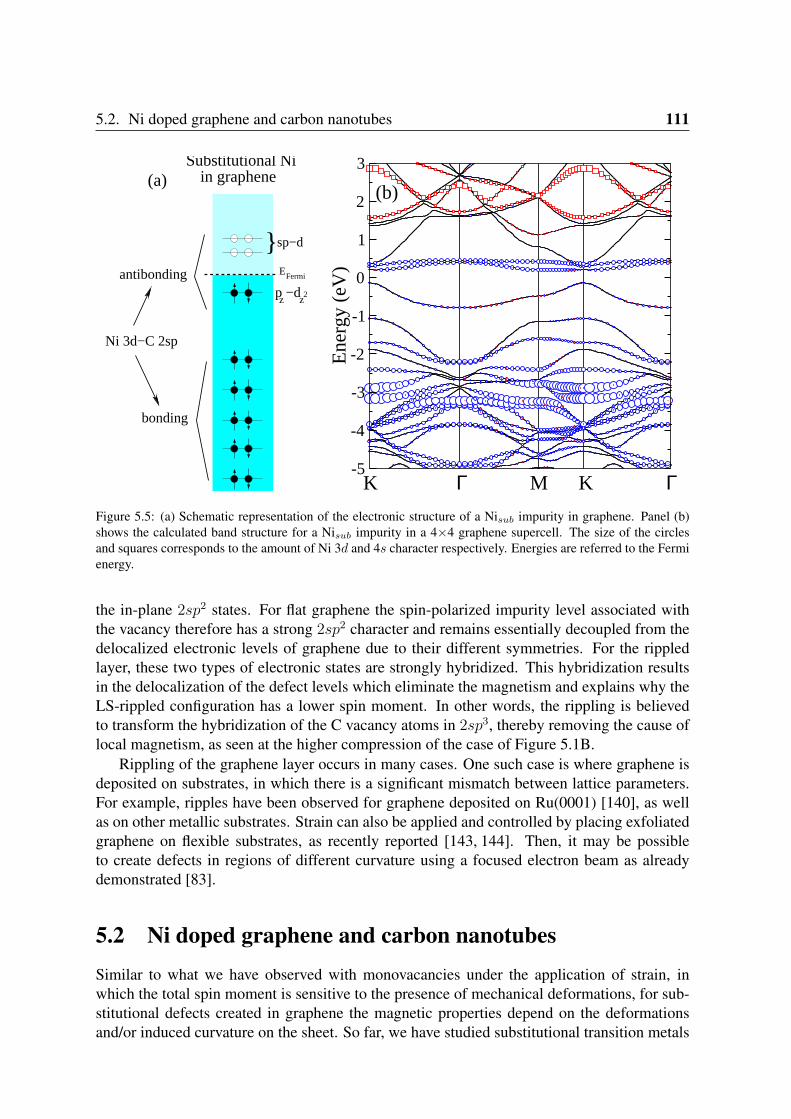
5.2. Ni doped graphene and carbon nanotubes 111
EFermi
(a)
sp−d
in graphene Substitutional Ni
antibonding
bonding
Ni 3d−C 2sp
p −d
2z z
-5
-4
-3
-2
-1
0
1
2
3
Ene
rgy
(eV
)
Γ ΓK KM
(b)
Figure 5.5: (a) Schematic representation of the electronic structure of a Nisub impurity in graphene. Panel (b)shows the calculated band structure for a Nisub impurity in a 4×4 graphene supercell. The size of the circlesand squares corresponds to the amount of Ni 3d and 4s character respectively. Energies are referred to the Fermienergy.
the in-plane 2sp2 states. For flat graphene the spin-polarized impurity level associated withthe vacancy therefore has a strong 2sp2 character and remains essentially decoupled from thedelocalized electronic levels of graphene due to their different symmetries. For the rippledlayer, these two types of electronic states are strongly hybridized. This hybridization resultsin the delocalization of the defect levels which eliminate the magnetism and explains why theLS-rippled configuration has a lower spin moment. In other words, the rippling is believedto transform the hybridization of the C vacancy atoms in 2sp3, thereby removing the cause oflocal magnetism, as seen at the higher compression of the case of Figure 5.1B.
Rippling of the graphene layer occurs in many cases. One such case is where graphene isdeposited on substrates, in which there is a significant mismatch between lattice parameters.For example, ripples have been observed for graphene deposited on Ru(0001) [140], as wellas on other metallic substrates. Strain can also be applied and controlled by placing exfoliatedgraphene on flexible substrates, as recently reported [143, 144]. Then, it may be possibleto create defects in regions of different curvature using a focused electron beam as alreadydemonstrated [83].
5.2 Ni doped graphene and carbon nanotubesSimilar to what we have observed with monovacancies under the application of strain, inwhich the total spin moment is sensitive to the presence of mechanical deformations, for sub-stitutional defects created in graphene the magnetic properties depend on the deformationsand/or induced curvature on the sheet. So far, we have studied substitutional transition metals
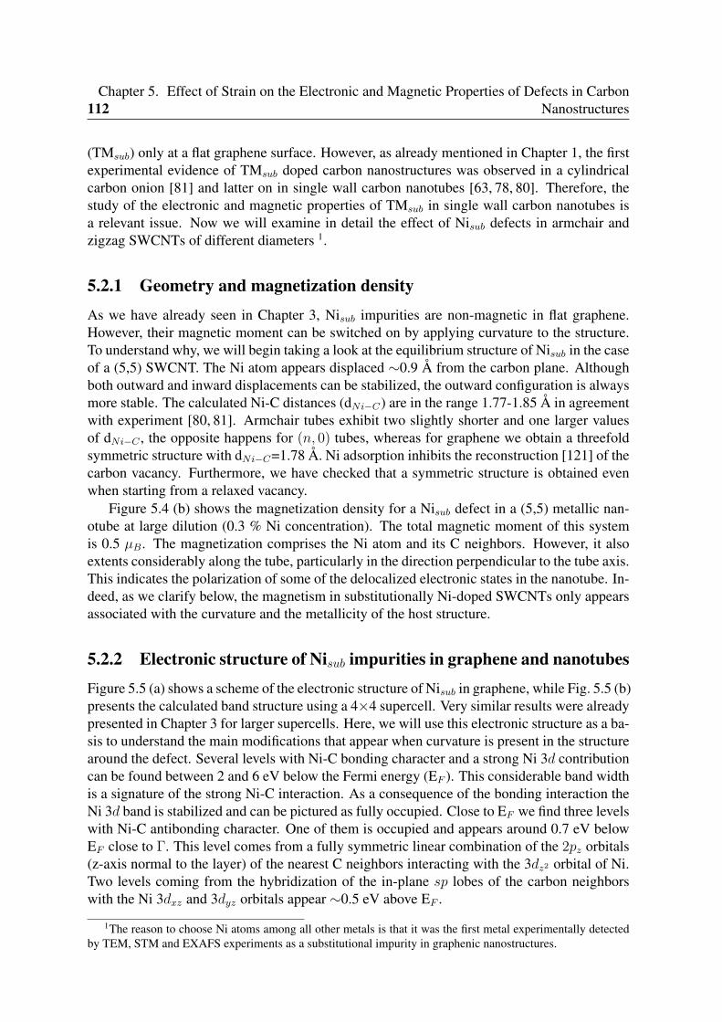
112Chapter 5. Effect of Strain on the Electronic and Magnetic Properties of Defects in Carbon
Nanostructures
(TMsub) only at a flat graphene surface. However, as already mentioned in Chapter 1, the firstexperimental evidence of TMsub doped carbon nanostructures was observed in a cylindricalcarbon onion [81] and latter on in single wall carbon nanotubes [63, 78, 80]. Therefore, thestudy of the electronic and magnetic properties of TMsub in single wall carbon nanotubes isa relevant issue. Now we will examine in detail the effect of Nisub defects in armchair andzigzag SWCNTs of different diameters 1.
5.2.1 Geometry and magnetization density
As we have already seen in Chapter 3, Nisub impurities are non-magnetic in flat graphene.However, their magnetic moment can be switched on by applying curvature to the structure.To understand why, we will begin taking a look at the equilibrium structure of Nisub in the caseof a (5,5) SWCNT. The Ni atom appears displaced ∼0.9 Å from the carbon plane. Althoughboth outward and inward displacements can be stabilized, the outward configuration is alwaysmore stable. The calculated Ni-C distances (dNi−C) are in the range 1.77-1.85 Å in agreementwith experiment [80, 81]. Armchair tubes exhibit two slightly shorter and one larger valuesof dNi−C , the opposite happens for (n, 0) tubes, whereas for graphene we obtain a threefoldsymmetric structure with dNi−C=1.78 Å. Ni adsorption inhibits the reconstruction [121] of thecarbon vacancy. Furthermore, we have checked that a symmetric structure is obtained evenwhen starting from a relaxed vacancy.
Figure 5.4 (b) shows the magnetization density for a Nisub defect in a (5,5) metallic nan-otube at large dilution (0.3 % Ni concentration). The total magnetic moment of this systemis 0.5 µB. The magnetization comprises the Ni atom and its C neighbors. However, it alsoextents considerably along the tube, particularly in the direction perpendicular to the tube axis.This indicates the polarization of some of the delocalized electronic states in the nanotube. In-deed, as we clarify below, the magnetism in substitutionally Ni-doped SWCNTs only appearsassociated with the curvature and the metallicity of the host structure.
5.2.2 Electronic structure of Nisub impurities in graphene and nanotubes
Figure 5.5 (a) shows a scheme of the electronic structure of Nisub in graphene, while Fig. 5.5 (b)presents the calculated band structure using a 4×4 supercell. Very similar results were alreadypresented in Chapter 3 for larger supercells. Here, we will use this electronic structure as a ba-sis to understand the main modifications that appear when curvature is present in the structurearound the defect. Several levels with Ni-C bonding character and a strong Ni 3d contributioncan be found between 2 and 6 eV below the Fermi energy (EF ). This considerable band widthis a signature of the strong Ni-C interaction. As a consequence of the bonding interaction theNi 3d band is stabilized and can be pictured as fully occupied. Close to EF we find three levelswith Ni-C antibonding character. One of them is occupied and appears around 0.7 eV belowEF close to Γ. This level comes from a fully symmetric linear combination of the 2pz orbitals(z-axis normal to the layer) of the nearest C neighbors interacting with the 3dz2 orbital of Ni.Two levels coming from the hybridization of the in-plane sp lobes of the carbon neighborswith the Ni 3dxz and 3dyz orbitals appear ∼0.5 eV above EF .
1The reason to choose Ni atoms among all other metals is that it was the first metal experimentally detectedby TEM, STM and EXAFS experiments as a substitutional impurity in graphenic nanostructures.
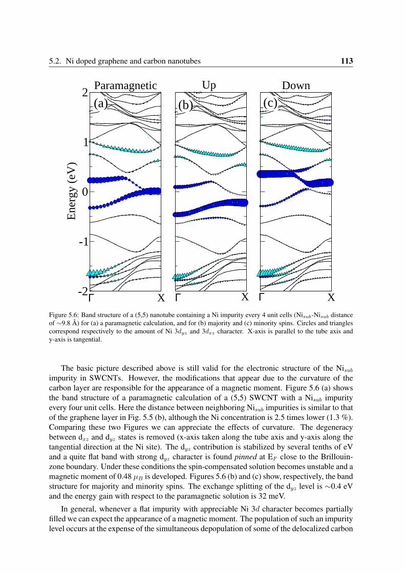
5.2. Ni doped graphene and carbon nanotubes 113
-2
-1
0
1
2
Ene
rgy
(eV
)Paramagnetic Up Down
Γ X X XΓ Γ
(a) (b) (c)
Figure 5.6: Band structure of a (5,5) nanotube containing a Ni impurity every 4 unit cells (Nisub-Nisub distanceof ∼9.8 Å) for (a) a paramagnetic calculation, and for (b) majority and (c) minority spins. Circles and trianglescorrespond respectively to the amount of Ni 3dyz and 3dxz character. X-axis is parallel to the tube axis andy-axis is tangential.
The basic picture described above is still valid for the electronic structure of the Nisub
impurity in SWCNTs. However, the modifications that appear due to the curvature of thecarbon layer are responsible for the appearance of a magnetic moment. Figure 5.6 (a) showsthe band structure of a paramagnetic calculation of a (5,5) SWCNT with a Nisub impurityevery four unit cells. Here the distance between neighboring Nisub impurities is similar to thatof the graphene layer in Fig. 5.5 (b), although the Ni concentration is 2.5 times lower (1.3 %).Comparing these two Figures we can appreciate the effects of curvature. The degeneracybetween dxz and dyz states is removed (x-axis taken along the tube axis and y-axis along thetangential direction at the Ni site). The dyz contribution is stabilized by several tenths of eVand a quite flat band with strong dyz character is found pinned at EF close to the Brillouin-zone boundary. Under these conditions the spin-compensated solution becomes unstable and amagnetic moment of 0.48 µB is developed. Figures 5.6 (b) and (c) show, respectively, the bandstructure for majority and minority spins. The exchange splitting of the dyz level is ∼0.4 eVand the energy gain with respect to the paramagnetic solution is 32 meV.
In general, whenever a flat impurity with appreciable Ni 3d character becomes partiallyfilled we can expect the appearance of a magnetic moment. The population of such an impuritylevel occurs at the expense of the simultaneous depopulation of some of the delocalized carbon
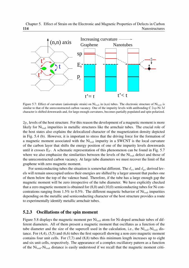
114Chapter 5. Effect of Strain on the Electronic and Magnetic Properties of Defects in Carbon
Nanostructures
tt’
t’ pz
EF
(n,n) axis
t’= t t’< t
sp
Graphene NanotubesIncreasing curvature
Figure 5.7: Effect of curvature (anisotropic strain) on Nisub in (n,n) tubes. The electronic structure of Nisub issimilar to that of the unreconstructed carbon vacancy. One of the impurity levels with antibonding C 2sp-Ni 3dcharacter is shifted downwards and, for large enough curvatures, becomes partially populated and spin-polarized.
2pz levels of the host structure. For this reason the development of a magnetic moment is morelikely for Nisub impurities in metallic structures like the armchair tubes. The crucial role ofthe host states also explains the delocalized character of the magnetization density depictedin Fig. 5.4 (b). However, it is important to stress that the driving force for the formation ofa magnetic moment associated with the Nisub impurity in a SWCNT is the local curvatureof the carbon layer that shifts the energy position of one of the impurity levels downwardsuntil it crosses EF . A schematic representation of this phenomenon can be found in Fig. 5.7where we also emphasize the similarities between the levels of the Nisub defect and those ofthe unreconstructed carbon vacancy. At large tube diameters we must recover the limit of flatgraphene with zero magnetic moment.
For semiconducting tubes the situation is somewhat different. The dxz and dyz derived lev-els will remain unoccupied unless their energies are shifted by a larger amount that pushes oneof them below the top of the valence band. Therefore, if the tube has a large enough gap themagnetic moment will be zero irrespective of the tube diameter. We have explicitly checkedthat a zero magnetic moment is obtained for (8,0) and (10,0) semiconducting tubes for Ni con-centrations ranging from 1.5% to 0.5%. The different magnetic behavior of Nisub impuritiesdepending on the metallic and semiconducting character of the host structure provides a routeto experimentally identify metallic armchair tubes.
5.2.3 Oscillations of the spin momentFigure 5.8 displays the magnetic moment per Nisub atom for Ni-doped armchair tubes of dif-ferent diameters. All of them present a magnetic moment that oscillates as a function of thetube diameter and the size of the supercell used in the calculation, i.e., the Nisub-Nisub dis-tance. For (4,4), (5,5) and (6,6) tubes the first supercell showing a non-zero magnetic momentcontains four unit cells. For (7,7) and (8,8) tubes this minimum length increases up to eightand six unit cells, respectively. The appearance of a complex oscillatory pattern as a functionof the Nisub-Nisub distance is easily understood if we recall that the magnetic moment criti-
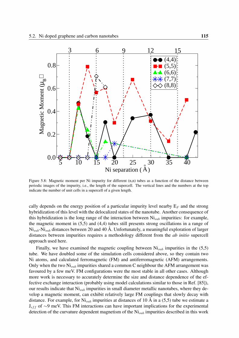
5.2. Ni doped graphene and carbon nanotubes 115
5 10 15 20 25 30 35 40Ni separation ( )
0.0
0.2
0.4
0.6
0.8
Mag
netic
Mom
ent (
µ Β)
(4,4)(5,5)(6,6)(7,7)(8,8)
Ao
3 6 9 12 15
Figure 5.8: Magnetic moment per Ni impurity for different (n,n) tubes as a function of the distance betweenperiodic images of the impurity, i.e., the length of the supercell. The vertical lines and the numbers at the topindicate the number of unit cells in a supercell of a given length.
cally depends on the energy position of a particular impurity level nearby EF and the stronghybridization of this level with the delocalized states of the nanotube. Another consequence ofthis hybridization is the long range of the interaction between Nisub impurities: for example,the magnetic moment in (5,5) and (4,4) tubes still presents strong oscillations in a range ofNisub-Nisub distances between 20 and 40 Å. Unfortunately, a meaningful exploration of largerdistances between impurities requires a methodology different from the ab initio supercellapproach used here.
Finally, we have examined the magnetic coupling between Nisub impurities in the (5,5)tube. We have doubled some of the simulation cells considered above, so they contain twoNi atoms, and calculated ferromagnetic (FM) and antiferromagnetic (AFM) arrangements.Only when the two Nisub impurities shared a common C neighbour the AFM arrangement wasfavoured by a few meV. FM configurations were the most stable in all other cases. Althoughmore work is necessary to accurately determine the size and distance dependence of the ef-fective exchange interaction (probably using model calculations similar to those in Ref. [85]),our results indicate that Nisub impurities in small diameter metallic nanotubes, where they de-velop a magnetic moment, can exhibit relatively large FM couplings that slowly decay withdistance. For example, for Nisub impurities at distances of 10 Å in a (5,5) tube we estimate aJeff of ∼9 meV. This FM interactions can have important implications for the experimentaldetection of the curvature dependent magnetism of the Nisub impurities described in this work
116Chapter 5. Effect of Strain on the Electronic and Magnetic Properties of Defects in Carbon
Nanostructures
and its influence in the observation of magnetism in carbon nanotube samples.
5.3 Uniaxial strain in Ni doped graphene
In this section we study the effect of uniaxial strain on the electronic structure of Nisub defectsin graphene. We find that the magnetic moment of Ni-doped graphene can be controlled byapplying a tensile strain along the zigzag and armchair direction. The spin moment of thesystem and its stability is greatly enhanced. At zero strain, Nisub defects are non-magnetic[113], but develop a spin moment that increases nearly linearly as a function of the uniaxialstrain. The changes are more dramatic when graphene reaches a critical strain (∼7.0%) aroundwhich an abrupt increase of the spin moment is observed. This magnetoelastic effect can beutilized to design a strain-tunable spin device based on defective graphene. We also propose anexperimental set up based on a scanning tunneling microscopy with a magnetic tip and using aflexible substrate on top of which graphene is deposited, allowing for the direct measurementof the observed magnetic switch effect.
5.3.1 Effect of uniaxial strain on the spin moment
Figures 5.9 (a)-(b) show the spin moment of a Nisub defect as a function of applied strain alongthe (n, n) and (n, 0) directions, respectively. The curves with filled squares show simulationsusing geometries from a non-spin polarized calculation with a DZ basis set. The spin momentand electronic structure are always calculated using a DZP basis. The open squares indicatesystems that were calculated using the previous procedure, i.e. a DZ basis, but the geome-tries have been obtained from spin-polarized calculations. The triangles display calculationswith DZP basis set for both geometry and spin moment. At zero strain the Nisub defect isnon-magnetic as was previously analyzed in previous sections (Section 5.2). As the uniaxialtension is applied, the system starts to deform. We see that at ∼3.5% strain the system becomesmagnetic with a magnetic moment that evolves nearly linearly with the uniaxial strain up tovalues of ∼ 0.30−0.40 µB at ∼6.0%. In spite of using different basis set (see caption in Figure5.9), all calculations present a very similar behaviour. At ∼6.8% the spin moment increasessharply from ∼0.40 µB to ∼1.9 µB. The transition is similar for both directions, although it issomewhat more abrupt along the (n, n) direction (Figure 5.9(a)) where no intermediate stepsare observed. This suggest that the local defect geometry and the defect orientation relativeto the applied strain play an important role to have magnetic properties. The insets I and IIin Figure 5.9(a)-(b) present the local defect geometry. When the strain is applied, the triangleformed by the three C neighboring atoms to the Ni impurity deforms. C-C distances alongthe strain direction increase, whereas distances along the perpendicular direction decrease inresponse to such elongation. The distance of the Ni atom to the first carbon neighbours alsoincreases, but this bond lenght changes for the studied strains are less than ∼5.0% (average onboth strain directions) in comparison with ∼20.0% for the C-C distances. We can concludethat there is a strong interaction between the carbon neighbours and the central Ni impurity,which is also reflected in the high stability of the defect. The formation energy for the Nisub
defect was observed to be highly favourable, with 7.9 eV binding energy to the vacancy.
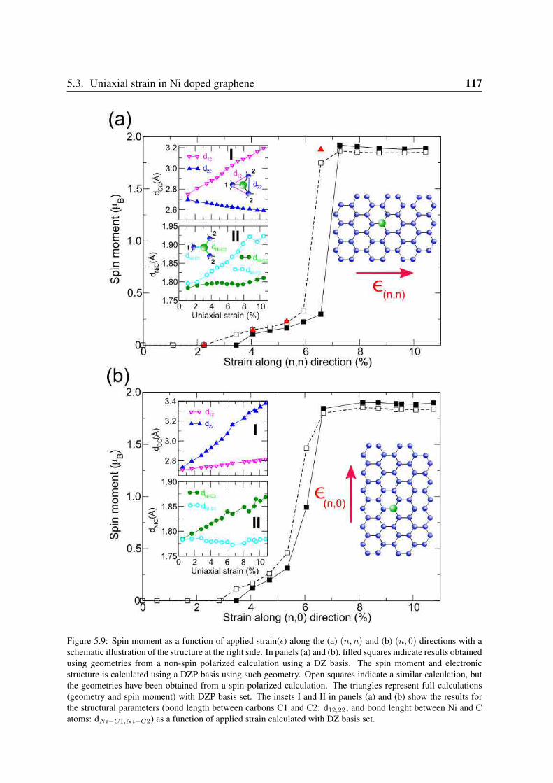
5.3. Uniaxial strain in Ni doped graphene 117
Figure 5.9: Spin moment as a function of applied strain(ϵ) along the (a) (n, n) and (b) (n, 0) directions with aschematic illustration of the structure at the right side. In panels (a) and (b), filled squares indicate results obtainedusing geometries from a non-spin polarized calculation using a DZ basis. The spin moment and electronicstructure is calculated using a DZP basis using such geometry. Open squares indicate a similar calculation, butthe geometries have been obtained from a spin-polarized calculation. The triangles represent full calculations(geometry and spin moment) with DZP basis set. The insets I and II in panels (a) and (b) show the results forthe structural parameters (bond length between carbons C1 and C2: d12,22; and bond lenght between Ni and Catoms: dNi−C1,Ni−C2) as a function of applied strain calculated with DZ basis set.
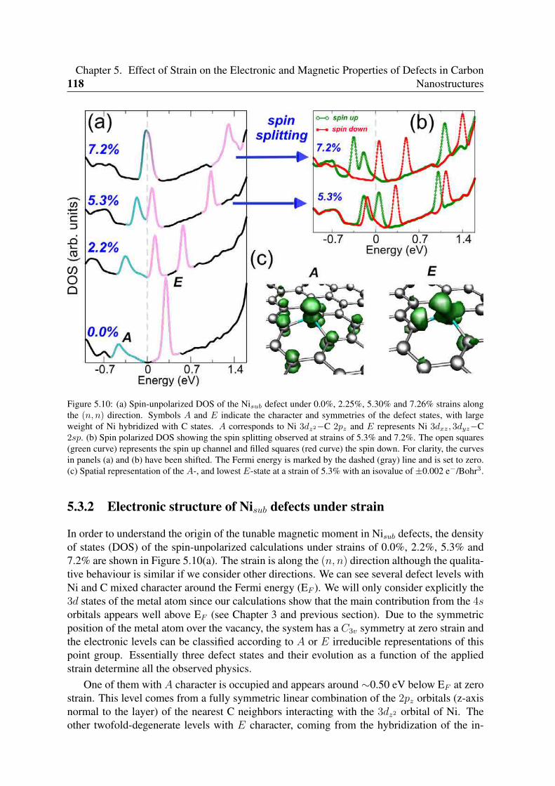
118Chapter 5. Effect of Strain on the Electronic and Magnetic Properties of Defects in Carbon
Nanostructures
Figure 5.10: (a) Spin-unpolarized DOS of the Nisub defect under 0.0%, 2.25%, 5.30% and 7.26% strains alongthe (n, n) direction. Symbols A and E indicate the character and symmetries of the defect states, with largeweight of Ni hybridized with C states. A corresponds to Ni 3dz2−C 2pz and E represents Ni 3dxz, 3dyz−C2sp. (b) Spin polarized DOS showing the spin splitting observed at strains of 5.3% and 7.2%. The open squares(green curve) represents the spin up channel and filled squares (red curve) the spin down. For clarity, the curvesin panels (a) and (b) have been shifted. The Fermi energy is marked by the dashed (gray) line and is set to zero.(c) Spatial representation of the A-, and lowest E-state at a strain of 5.3% with an isovalue of ±0.002 e−/Bohr3.
5.3.2 Electronic structure of Nisub defects under strain
In order to understand the origin of the tunable magnetic moment in Nisub defects, the densityof states (DOS) of the spin-unpolarized calculations under strains of 0.0%, 2.2%, 5.3% and7.2% are shown in Figure 5.10(a). The strain is along the (n, n) direction although the qualita-tive behaviour is similar if we consider other directions. We can see several defect levels withNi and C mixed character around the Fermi energy (EF ). We will only consider explicitly the3d states of the metal atom since our calculations show that the main contribution from the 4sorbitals appears well above EF (see Chapter 3 and previous section). Due to the symmetricposition of the metal atom over the vacancy, the system has a C3v symmetry at zero strain andthe electronic levels can be classified according to A or E irreducible representations of thispoint group. Essentially three defect states and their evolution as a function of the appliedstrain determine all the observed physics.
One of them with A character is occupied and appears around ∼0.50 eV below EF at zerostrain. This level comes from a fully symmetric linear combination of the 2pz orbitals (z-axisnormal to the layer) of the nearest C neighbors interacting with the 3dz2 orbital of Ni. Theother twofold-degenerate levels with E character, coming from the hybridization of the in-
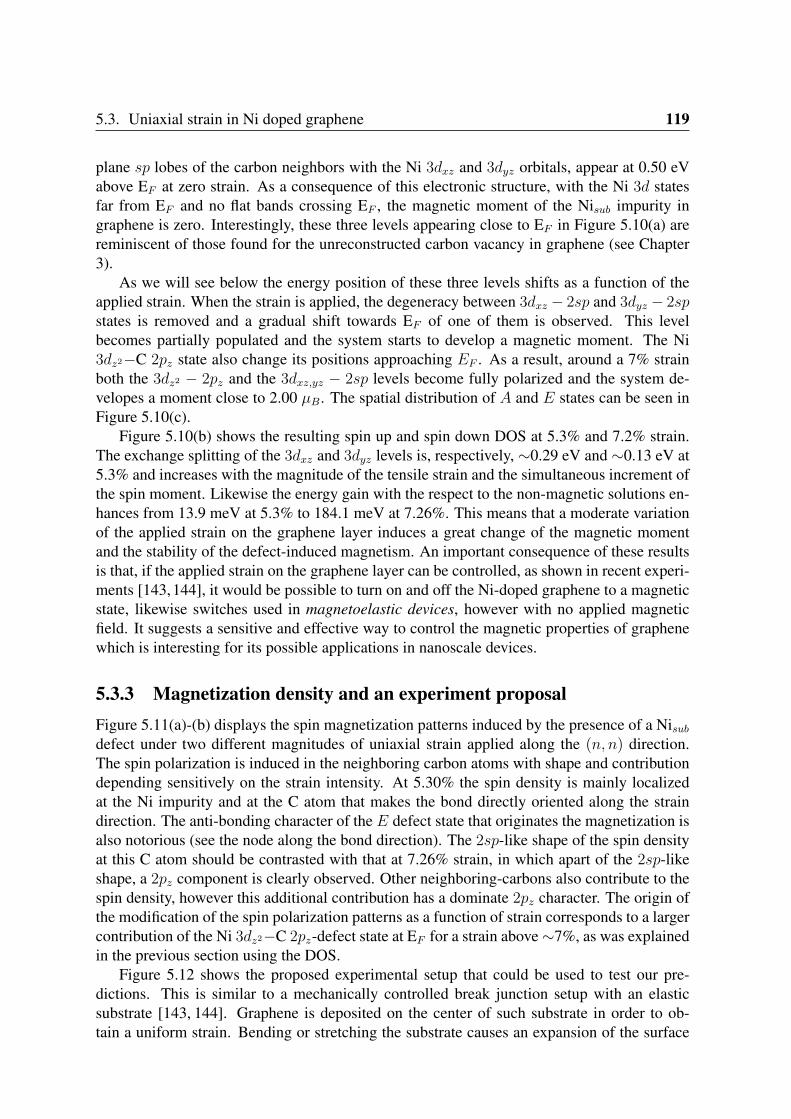
5.3. Uniaxial strain in Ni doped graphene 119
plane sp lobes of the carbon neighbors with the Ni 3dxz and 3dyz orbitals, appear at 0.50 eVabove EF at zero strain. As a consequence of this electronic structure, with the Ni 3d statesfar from EF and no flat bands crossing EF , the magnetic moment of the Nisub impurity ingraphene is zero. Interestingly, these three levels appearing close to EF in Figure 5.10(a) arereminiscent of those found for the unreconstructed carbon vacancy in graphene (see Chapter3).
As we will see below the energy position of these three levels shifts as a function of theapplied strain. When the strain is applied, the degeneracy between 3dxz − 2sp and 3dyz − 2spstates is removed and a gradual shift towards EF of one of them is observed. This levelbecomes partially populated and the system starts to develop a magnetic moment. The Ni3dz2−C 2pz state also change its positions approaching EF . As a result, around a 7% strainboth the 3dz2 − 2pz and the 3dxz,yz − 2sp levels become fully polarized and the system de-velopes a moment close to 2.00 µB. The spatial distribution of A and E states can be seen inFigure 5.10(c).
Figure 5.10(b) shows the resulting spin up and spin down DOS at 5.3% and 7.2% strain.The exchange splitting of the 3dxz and 3dyz levels is, respectively, ∼0.29 eV and ∼0.13 eV at5.3% and increases with the magnitude of the tensile strain and the simultaneous increment ofthe spin moment. Likewise the energy gain with the respect to the non-magnetic solutions en-hances from 13.9 meV at 5.3% to 184.1 meV at 7.26%. This means that a moderate variationof the applied strain on the graphene layer induces a great change of the magnetic momentand the stability of the defect-induced magnetism. An important consequence of these resultsis that, if the applied strain on the graphene layer can be controlled, as shown in recent experi-ments [143,144], it would be possible to turn on and off the Ni-doped graphene to a magneticstate, likewise switches used in magnetoelastic devices, however with no applied magneticfield. It suggests a sensitive and effective way to control the magnetic properties of graphenewhich is interesting for its possible applications in nanoscale devices.
5.3.3 Magnetization density and an experiment proposalFigure 5.11(a)-(b) displays the spin magnetization patterns induced by the presence of a Nisub
defect under two different magnitudes of uniaxial strain applied along the (n, n) direction.The spin polarization is induced in the neighboring carbon atoms with shape and contributiondepending sensitively on the strain intensity. At 5.30% the spin density is mainly localizedat the Ni impurity and at the C atom that makes the bond directly oriented along the straindirection. The anti-bonding character of the E defect state that originates the magnetization isalso notorious (see the node along the bond direction). The 2sp-like shape of the spin densityat this C atom should be contrasted with that at 7.26% strain, in which apart of the 2sp-likeshape, a 2pz component is clearly observed. Other neighboring-carbons also contribute to thespin density, however this additional contribution has a dominate 2pz character. The origin ofthe modification of the spin polarization patterns as a function of strain corresponds to a largercontribution of the Ni 3dz2−C 2pz-defect state at EF for a strain above ∼7%, as was explainedin the previous section using the DOS.
Figure 5.12 shows the proposed experimental setup that could be used to test our pre-dictions. This is similar to a mechanically controlled break junction setup with an elasticsubstrate [143, 144]. Graphene is deposited on the center of such substrate in order to ob-tain a uniform strain. Bending or stretching the substrate causes an expansion of the surface
120Chapter 5. Effect of Strain on the Electronic and Magnetic Properties of Defects in Carbon
Nanostructures
Figure 5.11: (a)-(b) Spin densities for Nisub defects at strains of 5.30% and 7.26% along the (n, n) direction. Thestrain direction is marked by the red arrows in both panels. The isovalue cutoff at (a) and (b) panels is ±0.035and ±0.060 e−/Bohr3.
and the deposited graphene will follow this deformation. In principle, the modifications onthe electronic structure can be detected using a scanning tunneling microscope (STM) sincethe defect levels that are involved are localized around the Fermi energy. If the magneticanisotropy of the defect is high enough, at sufficiently low temperatures, a preferential ori-entation of the moment would be stabilized and, therefore, a STM with a spin polarized tip(Spin-STM) could allow to monitor the evolution of the magnetic properties of the Ni-dopedgraphene with strain. Instead, an external magnetic field may be used to align the magneticmoment of the defects and define the hard/easy axis of the system. It is noteworth that thebreak junction-like setup has already been successfully used [145], and the STM capabilitiesfor the single-atom manipulation make the fabrication of the tip ending with magnetic atomsfeasible.
5.4 ConclusionsIn the present chapter, we have analyzed in detail the effect of different mechanical deforma-tions (isotropic strain, curvature and uniaxial strain) on the structural and magnetic propertiesof two types of defects, carbon monovacancies and Ni substitutional impurities in graphenicstructures. We have seen that mechanical deformations have a strong influence on the mag-netic properties of these defects. In some cases, like a Nisub impurity in graphene underuniaxial strain, this can be used to turn on and off the spin moment and can be of use in futurespintronic devices.
We have presented a first-principles density functional theory study of the carbon mono-vacancy in graphene under an applied strain. The stress was observed to play an importantrole in determining the electronic, geometrical and magnetic properties of this system. Wehave shown that the magnetic and structural properties of the carbon monovacancy exhibita strong dependence on the local curvature of the graphene layer at the defect position. This
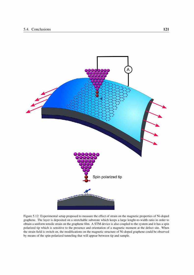
5.4. Conclusions 121
Figure 5.12: Experimental setup proposed to measure the effect of strain on the magnetic properties of Ni-dopedgraphene. The layer is deposited on a stretchable substrate which keeps a large lenght-to-width ratio in order toobtain a uniform tensile strain on the graphene film. A STM device is also coupled to the system and it has a spinpolarized tip which is sensitive to the presence and orientation of a magnetic moment at the defect site. Whenthe strain field is switch on, the modifications on the magnetic structure of Ni-doped graphene could be observedby means of the spin-polarized tunneling that will appear between tip and sample.
122Chapter 5. Effect of Strain on the Electronic and Magnetic Properties of Defects in Carbon
Nanostructures
curvature, along with the global rippling pattern, can be controlled by straining the layer. Witha compression of the layer up to 2% we can tune the spin moment of the vacancy between 0and 1.5 µB. This range of deformations can be accessible experimentally, and are comparableto those found for a graphene layer deposited on several substrates. From a more general per-spective, our results suggest that the magnetism induced in graphene by the presence of pointdefects can be controlled using isotropic strain and other mechanical deformation.
An important consequence of these results is that, due to the two dimensional characterof graphene and thus prompt to undergo bending and other deformations, it is difficult to talkabout the intrinsic electronic and magnetic properties of point defects like the monovacancy.To have a complete characterisation of the defect is necessary either to specify the local curva-ture of the layer at the defect position or to consider explicitly the stresses applied to the layer.This is in clear contrast to the case of three dimensional crystals, where elastic deformationsare typically much smaller.
Regarding our study of Nisub defects in graphene and SWCNT’s, the main conclusions forthis study are:
(i) the magnetic moment of substitutionally Ni-doped graphene can be controlled by ap-plying mechanical deformations that break the hexagonal symmetry of the layer, like curva-ture does. As we have already seen in Chapter 3, Nisub impurities are non-magnetic in flatgraphene. However, their magnetic moment can be switched on by applying curvature to thestructure. For metallic carbon nanotubes the curvature of the carbon layer around the de-fect can drive the transition of the Nisub impurities to a magnetic state. For semiconductingtubes, the Nisub impurities remain non-magnetic irrespective of the tube diameter. Therefore,the magnetic or non-magnetic character of Nisub impurities in metallic carbon nanostructurescan be controlled by the local curvature. This surprising result can be fully understood andrationalised from the electronic structure of the Nisub defect;
(ii) We have analyzed in detail the origin and distribution of the magnetic moment. Wefound that the formation of the magnetic moment associated with Nisub impurities is accompa-nied by the polarization of the delocalized electronic states of carbon layer. Furthermore, themagnetic moment of Nisub also becomes a signature of the metallicity of the structure: onlymetallic tubes develop a moment that depends on the tube diameter and Ni concentration;
(iii) The magnetic moment for armchair nanotubes as a function of the concentration ofNisub impurities shows a complex oscillatory behavior, which points to very long-range inter-actions between Nisub defects. We have also analyzed the magnetic couplings between Nisub
impurities in a (5,5) tube and found that they are predominantly ferromagnetic for the set ofstructures studied;
(iv) We found that Ni atoms have a very large affinity for carbon vacancies. Therefore,deposited Ni atoms on a graphene layer or carbon nanotube will present a strong tendencyto attach to existent carbon vacancies. This opens a route to fabricate structures where thephenomenology presented in this work can be experimentally explored in a controlled way.
(v) The electronic and magnetic structure of the Nisub defect strongly depends on uniaxialstrain. We observe that stretching the layer by a few percents along different crystalline direc-tions is enough to turn the non-magnetic ground state of Ni atoms embedded in graphene to amagnetic state.
(vi) The magnetic moment increases its magnitude and energetic stability with the appliedstrain. At a critical strain value of 6.8%, a transition is observed in the magnitude of spinmoment which is weakly dependent on the orientation of the applied strain. A detailed analysis
5.4. Conclusions 123
indicates that this strain-tunable magnetic moment is the result of changes in the position ofthree defect levels around Fermi energy which are antibonding combinations of the Ni 3dstates and the 2pz and 2sp orbitals of the neighboring C atoms.
(vii) The tunable magnetism observed in Nisub defects and its stability via strain controlmay play an interesting role in flexible spintronics devices. We also propose an experimentalsetup to measure this dependence based on a flexible substrate where graphene is depositedon top and a spin polarized STM device is used.
Our work predicts a complex magnetic behavior for Nisub impurities in carbon nanotubesand graphene. This investigation is highly relevant for the interpretation of experimental re-sults since it has been proposed that appreciable amounts of metal atoms can be incorporatedinto the carbon network, forming this type of substitutional defects, during synthesis and arevery difficult to eliminate afterwards. Furthermore, our results point to the existence of a largecoupling between the magnetic and elastic response in Ni-doped carbon nanostructures. Thiscan be of fundamental and technological interest and might be verified experimentally.

124Chapter 5. Effect of Strain on the Electronic and Magnetic Properties of Defects in Carbon
Nanostructures
Chapter 6
Summary and outlook
Graphenic nanostructures represent an important research subject in the fields of nanoscienceand nanotechnology. These materials possess extraordinary properties which are supposed torevolutionise the performance of electronic components in the next generation of electronicdevices. Several applications within electronics, materials science, condensed matter physics,etc, have been predicted or are already available [146]. The study of graphene has changedin recent years from a theoretical topic to a field where experimental and theoretical advancesgo hand in hand. In particular, the theoretical studies shown in this thesis are either linked ordirectly motivated by new experiments.
This thesis focuses on the modeling electronic and magnetic properties of defects in car-bon nanostructures. The SIESTA method, based on density functional theory (DFT), was usedas the main tool to compute all chemical and physical properties of the studied systems. Otherab initio method was also used in the simulations, the VASP code, which using a differentmethodology based on plane waves and projector-augmented wave potentials (PAW), allowsus to check the possible limitations of the pseudopotentials and localized basis set used inSIESTA. Remarkably, the agreement between both set of calculations is excellent. Otherprograms were also utilized to analyze and treat the huge amount of data obtained in the sim-ulations. From simple programs in AWK, PYTHON, FORTRAN, up to sophisticated graphicalpackages used to create some figures displayed in this thesis.
Our results have shown in Chapter 3, how the electronic (and mainly magnetic) proper-ties of a graphene monolayer can be modified by doping with substitutional transition metals(Msub). Some results of this chapter are the following:
• We have developed a model based on the hybridization between the states of the metalatom, particularly the d shell, and the defect levels associated with an unreconstructedD3h carbon vacancy. This allowed us to have a simple way to understand the trendsobserved for the bonding, energetics, and electronic and magnetic properties of severalmetal impurities in graphene.
• Using the previous model, we identified three different regimes associated with the oc-cupation of different carbon-metal hybridized electronic levels and we use them to clas-sify the substitutional dopants in graphene: bonding states (Sc, Ti), non-bonding states(V, Cr, Mn) and antibonding states (Fe, Co, Ni, Cu, Ag, Au, Zn).
• Consequently, Sc and Ti do not show a spin moment. On the contrary, V, Cr and Mn
125
126 Chapter 6. Summary and outlook
display spin moments of increasing size with a strong 3d component. Co, Ni, the noblemetals and Zn present an oscillatory behaviour of the spin moment between 0 and 1µB. The spin moment for these later impurities has a strong contribution from the Cneighbours in the layer.
• The Fe defect occupies a special position between the non-bonding and antibondingregimes. Their magnetic behavior stems from the competition between the carbon-metal hybridization and the electron-electron interaction within the 3d shell. AlthoughFe impurities are non-magnetic at the GGA level, GGA+U calculations with moderatevalues of U (above ∼2 eV) produce a spin-moment of 1 µB.
• Substitutional Zn atoms also display a peculiar behaviour because Jahn-Teller-like dis-tortions end in a zero spin moment. A symmetric configuration with a spin moment of2µB and a very small energy penalty of ∼150 meV has also been identified.
Many of the interesting results shown in this chapter are still waiting for experimental veri-fication. Some of these observations are consistent with the experimental data in the literature.For example, our energetic and structural analysis agree with recent experiments [63, 78, 80].The analysis shown here might be important to understand the doping by transition metals inother carbon nanostructures.
In Chapter 4 we have studied the electronic structure and magnetic properties, includingexchange couplings, of several defects in graphene. These can be approximately mappedonto a monovacancy in graphene calculated by a π-tight-binding model. Such systems areCo substitutional impurities (Cosub), several adsorbates chemisorbed on graphene through asingle covalent C-C bond.
The main results of this chapter can be summarised in the following:
• At either Cosub orC−X defects, the observed magnetic behaviour follows that observedfor a single π-vacancy in a simple tight-binding model of graphene. The electronicstructure of both defects nearby the Fermi energy is dominated by a single level with astrong contribution from the pz orbitals of the neighboring C atoms.
• The Cosub or C − X isolated defects show a spin moment of 1.0 µB. When severaldefects are present, the spin moment follows closely Lieb’s theorem for bipartite latticesand depends on the number of defects in each sublattice.
• The magnetic couplings are predominantly (anti)ferromagnetic for Cosub defects sitedin the (opposite) same sublattice. However, some differences for C − X defects wereobserved and adsorbates at different sublattices always converge to non-magnetic solu-tions.
• A RKKY-like model was used to fit the magnetic interactions obtained from DFT calcu-lations for both Cosub and C −X defects. This model pointed out that the dependenceof the exchange constants on the distance between defects differ for Co atoms and ad-sorbed molecules. The interaction between chemisorbed molecules on top of a C atomin graphene surface is long range and falls off slowly with the distance, roughly pro-portional to JAA(rij) ∼ |rij|−(1+ϵ) with |ϵ| ∼ 0.20, where JAA(rij) are the exchangeconstant for defects at the same graphenic sublattice. For Cosub defect the magnetic
127
interactions decay faster and have a distance dependence given by JAA(rij) ∼ |rij|−2.43.This means that although the spin moment for both defects has a similar origin, the 3dcomponent of the Co dopants and slightly more localized character modifies the inter-actions.
• For Cosub impurities it is possible to stabilize antiferromagnetic solutions for A-B con-figurations. Exchange couplings for such configurations show a complex behaviour witha strong anisotropy, dependent on the relative positions of the dopants, along certaincrystalline directions.
In Chapter 5 we have studied the effect of strain on the electronic and magnetic propertiesof substitutional Ni impurities (Nisub) and vacancies in graphenic nanostructures. One of themain results of this part is that mechanical deformations (similar to those induced by substrateswhen graphene is deposited on top of them or the curvature present in carbon nanotubes)can be used to control the magnetism of defects in graphene. The proposed models takeinto account the interplay of corrugations, defect formation and magnetism. They open newopportunities for engineering carbon material properties using strain and defects. We believethat strain will play a key role in flexible electronics, in which graphene is one of the maincandidates.
In more detail, we found that:
• Biaxial strain applied to monovacancies in graphene was observed to play an importantrole in determining the electronic, geometrical and magnetic properties of this system.We have shown that the magnetic and structural properties of the carbon monovacancyexhibit a strong dependence on the local curvature of the graphene layer at the defectposition. This local curvature is strongly coupled to the global structure rippling of thelayer.
• Phase diagrams of the spin solutions and geometric configurations as a function of strainare presented for a monovacancy in graphene.
• Stretching increases the moment of different spin solutions and compression reducesor even kills the magnetic polarization. The transition to a non-magnetic solution islinked to changes in the local structure of the defect which are driven by modificationsin the global structure of graphene that are associated with the formation of long rangeripples. For compressions slightly greater than 3%, this rippling leads to the formationof a heavily reconstructed vacancy structure at a saddle point position consisting of twotwisted hexagons and pentagons.
• For metallic carbon nanotubes the curvature of the carbon layer around the defect candrive the transition of the Nisub defect to a magnetic state (Nisub defects are non-magneticin flat graphene). For semiconducting tubes, however, the Nisub impurities remain non-magnetic irrespective of the tube diameter.
• Therefore, the magnetic or non-magnetic character of Nisub impurities in metallic carbonnanostructures can be controlled by the local curvature. This surprising result can befully understood and rationalised from the electronic structure of the Nisub defect.
128 Chapter 6. Summary and outlook
• The different magnetic behavior of Nisub dopants depending on the metallic and semi-conducting character of the host structure might provide a route to experimentally iden-tify metallic armchair tubes.
• The magnetic moment for armchair nanotubes as a function of the concentration of Niatoms shows a complex oscillatory behavior, which points to very long-range interac-tions between Nisub defects. We have analyzed the magnetic couplings between Niimpurities in a (5,5) tube and found that they are predominantly ferromagnetic for thestudied structures.
• The effect of uniaxial strain on Nisub shows that the magnetic moment can be controlledby applying a tensile strain.
• At zero strain, Nisub defects are non-magnetic but develop a spin moment that increasesnearly linear as a function of uniaxial strain. The changes are more dramatic when acritical strain value (∼6-7%) is reached, around which an abrupt transition of the spinmoment is observed.
• This magnetoelastic-like effect can be utilized to design a strain-tunable spin devicesbased on Ni-doped graphene.
6.1 OutlookWhile the major part of this thesis has focused on the analysis of defects and their interactionwith the host material, which we believe is relevant for many theoreticians and experimen-talists, part of the physical results and interpretations have not been experimentally validatedto date. We believe, however, that this will happen sooner rather than later due to the rapidadvances in the field.
In fact, day-by-day better experimental control of precise and reproducible doping, sur-face and defect engineering, and growth process will enable a closer comparison betweenexperiments and our theoretical models. The recent developments of graphene, pushed aheadby observed, expected, and hoped new physics, is the great driving force for research in thisbranch of carbon nanoscience. For example, in the last few months before the end of thismanuscript we have found experimental evidences of one of our predictions: The direct mea-surement of spin signal, at room temperature, in partially hydrogenated graphene samplesusing a superconducting quantum interference devices (SQUID) [147]. The realization ofsuch ferromagnetic order in purely sp−based materials will be of importance in many areasrelated to spintronics, even more if the other adsorbates, as pointed out in this thesis, presenta similar behaviour.
The immediate continuation of the work presented in this thesis should include the elec-tron and phonon transport properties under the presence of substitutional metals defects ingraphene as well as in carbon nanotubes. In particular, a collaboration with Prof. MadsBrandbyge at Danish Technical University (DTU), in Lyngby, Denmark, has been stablishedin order to calculate the scattering properties of such metal impurities in graphenic structuresand the results will be published elsewhere [148].
6.1. Outlook 129
Another field of research in which the interplay of strain, the presence of defects and mag-netism will play a role is in spin transport. Due to the low spin-orbit coupling in C, longspin-coherence times are expected, which might be of importance for spin polarized currentsgenerated by carbon defects or adsorbates in graphenic nanostructures. If strain could be usedto polarize an electric current when it interacts with a localized spin moment in the carbonhost, it would avoid using expensive ferromagnetic/antiferromagnetic leads in order to obtainpolarized currents and could provide a simple way to obtain spin-transport control.
At the same time, the effect of an external gate voltage on substitutional defects would beparticularly relevant. For practical purposes, the use of electric fields would be desirable astheir high-frequency generation is more readily achieved than for magnetic fields. Therefore,the ability to electrically control spin dynamics in defects makes it one of the most promisingplatforms for solid-state spin devices based on carbon [148].

130 Chapter 6. Summary and outlook
Appendix A
Publications
This is a list of publications.
12. †Gate-Field Controlled Spin Transport in Carbon Nanotubes Substitutionally Dopedwith Transition MetalsElton J. G. Santos, A. Ayuela, D. Sánchez-Portal and Mads BrandbygeIn preparation
11. †Photoluminiscence Emission in SWNT Covered with PMMA PolymerAinara Garcia-Gallastegui, Roberto Muños, Isabel Obieta, Izaskun Bustero, Jesus M.Aizpurua, Elton J. G. Santos, D. Sánchez-Portal and A. AyuelaSubmitted
10. †Magnetism of Covalently Functionalized Carbon NanotubesElton J. G. Santos, D. Sánchez-Portal and A. AyuelaAppl. Phys. Lett. 2011, 99, pp.062503-062506Also selected to Virtual Journal of Nanoscale Science and Technology 24, Issue 8 (2011)
9. †Universal Spin Moment in Covalently Functionalized GrapheneElton J. G. Santos, A. Ayuela and D. Sánchez-PortalSubmitted
8. †Strain-Tunable Spin Moment in Ni-Doped Graphene MonolayerElton J. G. Santos, A. Ayuela and D. Sánchez-PortalSubmitted
7. †Spin-Strain Phase Diagram of Defective GrapheneElton J. G. Santos, S. Riikonen, D. Sánchez-Portal and A. AyuelaarXiv:1012.3304v1
6. †Magnetism of Substitutional Co Impurities in Graphene: Realization of a Single πVacanciesElton J. G. Santos, D. Sánchez-Portal and A. AyuelaPhys. Rev. B 2010, 81, pp.125433-125439.
†Publication related to the thesis.
131
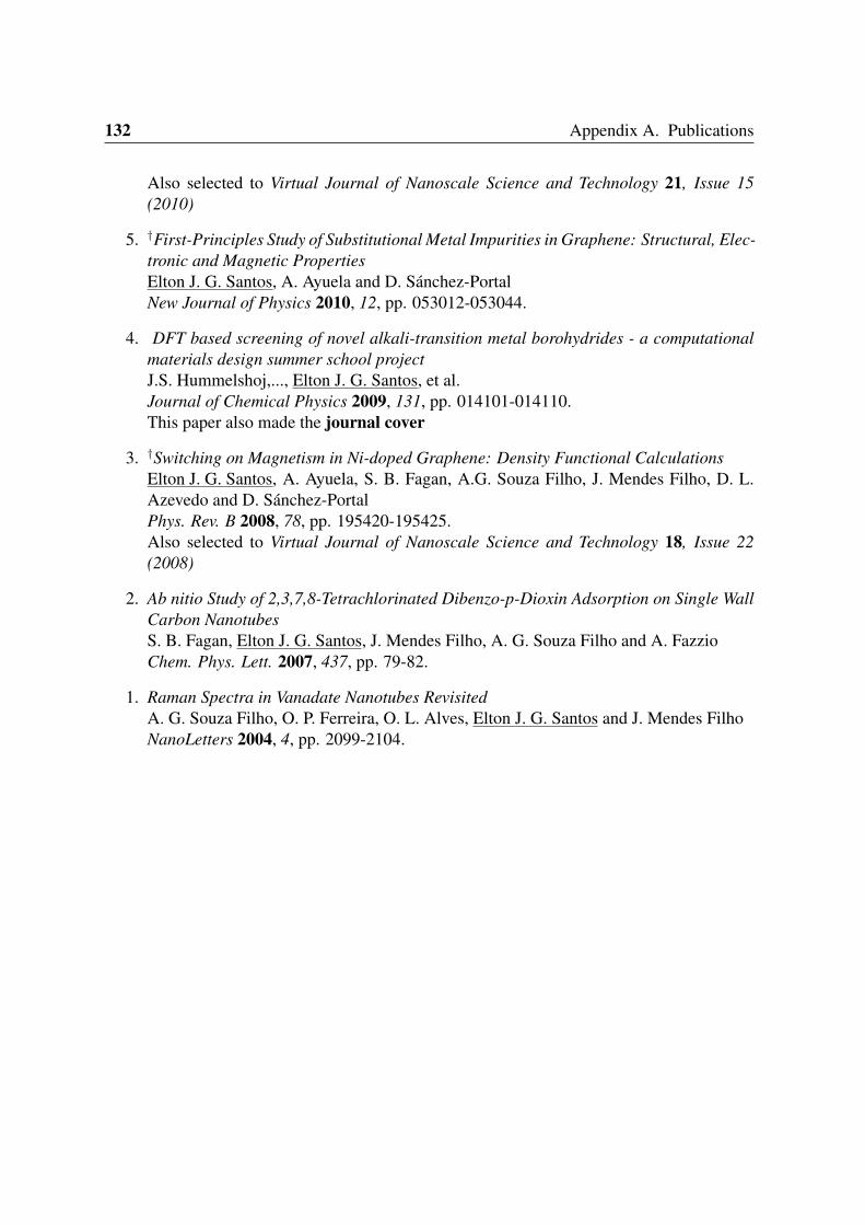
132 Appendix A. Publications
Also selected to Virtual Journal of Nanoscale Science and Technology 21, Issue 15(2010)
5. †First-Principles Study of Substitutional Metal Impurities in Graphene: Structural, Elec-tronic and Magnetic PropertiesElton J. G. Santos, A. Ayuela and D. Sánchez-PortalNew Journal of Physics 2010, 12, pp. 053012-053044.
4. DFT based screening of novel alkali-transition metal borohydrides - a computationalmaterials design summer school projectJ.S. Hummelshoj,..., Elton J. G. Santos, et al.Journal of Chemical Physics 2009, 131, pp. 014101-014110.This paper also made the journal cover
3. †Switching on Magnetism in Ni-doped Graphene: Density Functional CalculationsElton J. G. Santos, A. Ayuela, S. B. Fagan, A.G. Souza Filho, J. Mendes Filho, D. L.Azevedo and D. Sánchez-PortalPhys. Rev. B 2008, 78, pp. 195420-195425.Also selected to Virtual Journal of Nanoscale Science and Technology 18, Issue 22(2008)
2. Ab nitio Study of 2,3,7,8-Tetrachlorinated Dibenzo-p-Dioxin Adsorption on Single WallCarbon NanotubesS. B. Fagan, Elton J. G. Santos, J. Mendes Filho, A. G. Souza Filho and A. FazzioChem. Phys. Lett. 2007, 437, pp. 79-82.
1. Raman Spectra in Vanadate Nanotubes RevisitedA. G. Souza Filho, O. P. Ferreira, O. L. Alves, Elton J. G. Santos and J. Mendes FilhoNanoLetters 2004, 4, pp. 2099-2104.
Appendix B
Conference and Workshop Contributions
39. Magnetism of Graphene with Defects: Vacancies, Substitutional Metals and CovalentFunctionalization. Workshop on Graphene, Donostia-San Sebastian, Spain. August29th - September 2nd 2011.Poster section
38. Magnetism in Graphene Induced by Defects. Workshop on Graphene, Donostia-SanSebastian, Spain. August 29th - September 2nd 2011.Oral section by Elton J. G. Santos
37. Magnetism of Graphene with Defects: Vacancies, Substitutional Metals and CovalentFunctionalization. PCAM Summer School 2011: Electronic and Optical Properties ofNanoscale Materials. Donostia-San Sebastian, Spain. July 4th - 7th 2011.Poster section
36. Spin-Strain Phase Diagram of Defective Graphene. PCAM Summer School 2011: Elec-tronic and Optical Properties of Nanoscale Materials, Donostia-San Sebastian, Spain.July 4th - 7th 2011.Oral section presented by Elton J. G. Santos
35. Magnetism in Graphene Induced by Defects. The 29th International Brand RitchieWorkshop (BRW2011) on Particle Penetration Phenomena and Excitations of Solids,Matsue, Shimane, Japan. May 12nd - 15th 2011.Oral section presented by A. Ayuela (Invited talk)
34. Magnetism of Covalently Functionalized Graphene. Graphene 2011, Bilbao, Spain.April 11st - 14th 2011.Oral section presented by D. Sánchez-Portal
33. Magnetism of Graphene with Defects: Vacancies, Substitutional Metals and CovalentFunctionalization. Graphene 2011, Bilbao, Spain. April 11st - 14th 2011.Poster section
32. Magnetism of Covalently Functionalized Graphene. 3S’11: Symposium on SurfaceScience 2011, Baqueira Beret, Lleida, Spain. March 6th - 12nd 2011.Oral section presented by D. Sánchez-Portal
133
134 Appendix B. Conference and Workshop Contributions
31. Spin-Strain Phase Diagram of Defective Graphene. 5th International Meeting on Molec-ular Electronics - ElecMol 10, Grenoble, France. December 6th - 10th 2010.Specially selected for Oral section, presentation by Elton J. G. Santos
30. Spin-Strain Phase Diagram of Defective Graphene. Passion for knowledge: The Work-shops, San Sebastian, Spain. September 27th - October 1st 2010.Poster section
29. Graphene Interacting with Transition Metals: Tuning the Electronic and Magnetic Prop-erties of Graphene. Passion for knowledge: The Workshops, San Sebastian, Spain.September 27th - October 1st 2010.Oral section presented by D. Sánchez-Portal (Invited talk)
28. Substitutional Atoms in Graphene: Vacancy States Versus Metal Bonding. GrapheneWeek 2010, College Park, Maryland, USA. April 19th - 23rd 2010.Poster section
27. Electronic Structure of Graphene Interacting with Transition Metals: SubstitutionalDefects and Graphene/Ru(0001). CIC nanoGUNE Consolider, San Sebastian, Spain.March 29th 2010.Seminar presented by D. Sánchez-Portal
26. Electronic Properties of Substitutional Transition Metals in Graphenic Carbon: Mag-netism, Trends and Surprises. NordForsk Spintronics Workshop, Copenhagen - Lyngby,Denmark. October 29-30th 2009.Oral section presented by Elton J. G. Santos (Invited talk)
25. Electronic Properties of Substitutional Transition Metals in Graphenic Carbon: Mag-netism, Trends and Surprises. Graphene Mini-Workshop 2009, Copenhagen - Lyngby,Denmark. October 23rd 2009.Oral section presented by Elton J. G. Santos (Invited talk)
24. On the Magnetism of Substitutional Transition-Metal Impurities in Graphenic Nanos-tructures. TNT09 - Trends in Nanotechnology, Barcelona, Spain. September 7th - 11st2009.Poster section
23. Magnetism of Substitutional Co Impurities in Graphene: Realization of a Single π-Vacancy. Nanotec09 - 11th International Conference on Nanotechnology in Carbon andRelated Materials, Brussels, Belgium. August 26th-29th, 2009.Poster section
22. Magnetism of Graphene and Carbon Nanotubes Substitutionally Doped with CataliticMetals. NanoteC09 - 11th International Conference on Nanotechnology in Carbon andRelated Materials, Brussels, Belgium. August 26th-29th, 2009.Oral section presented by Elton J. G. Santos
135
21. Magnetism of Substitutional Co Impurities in Graphene: Realization of Single Vacan-cies. NT09: Tenth International Conference on the Science and Application of Nan-otubes, Beijing, China. June 21st-26th, 2009.Poster section
20. Substitutional Metal Atoms in Graphene: Vacancy States Versus Metal Bonding. CCTN09:Fifth International Symposium on Computational Challenges and Tools for Nanotubes,Beijing, China. June 20th, 2009.Oral section presented by A. Ayuela (Invited talk)
19. Magnetism of Graphene and Carbon Nanotubes Substitutionally Doped with Ni. FirstinanoGune Workshop, CIC - NanoGune, San Sebastian. Spain, May 25th - 26th 2009.Poster section
18. Magnetism of Graphene and Carbon Nanotubes Substitutionally Doped with Ni. DNC09- Computational Studies of Defects in Nanoscale Carbon Materials, CECAM-HQ-EPFL,Lausanne, Switzerland. May 11st - 13rd 2009.Poster section
17. Magnetism of Substitutional Transition-Metal Impurities in Graphenic Nanostructures.DNC09 - Computational Studies of Defects in Nanoscale Carbon Materials, CECAM-HQ-EPFL, Lausanne, Switzerland. May 11st - 13rd, 2009.Oral section presented by D. Sánchez-Portal (Invited talk)
16. On the Magnetism of Substitutional Transition-Metal Impurities in Graphenic Nanos-tructures. 14th International Workshop on Computational Physics and Materials Sci-ence: Total Energy and Force Methods, Trieste, Italy. January 8th - 11st 2009.Poster section
15. On the Magnetism of Substitutional Transition-Metal Impurities in Graphenic Nanos-tructures. TKK - Laboratory of Physics, Helsinki University of Technology, Helsinki,Finland. November 27th 2008.Seminar presented by D. Sánchez-Portal
14. On the Magnetism of Substitutional Transition-Metal Impurities in Graphenic Nanos-tructures. NanoSWEC - Nano South-West European Conference, Bordeaux, France.November 3rd - 5th 2008.Oral section presented by D. Sánchez-Portal (Invited talk)
13. Magnetism of Graphene Substitutionally Doped with Transition Metals. Symposium inhonour of Professor Agustin Del Moral, San Sebastian, Spain. September 22th 2008.Oral section presented by D. Sánchez-Portal (Invited talk)
12. Complex Magnetic Behaviour of Substitutional Ni Dopands in Graphenic Systems. IS-SPIC 2008 - International Symposium on Small Particles and Inorganic Clusters, Val-ladolid, Spain. September 15th - 19th 2008.Poster section

136 Appendix B. Conference and Workshop Contributions
11. Complex Magnetic Behaviour of Substitutional Ni Dopands in Carbon Nanotubes andGraphene. International CAMd 2008 Summer School, Copenhagen, Denmark. August18th - 30th 2008.Poster section
10. Complex Magnetic Behaviour of Substitutional Transition Metal Dopands in GraphenicSystems. NT08 - Ninth International Conference no the Science and Application ofNanotubes 2008, Le Corum, Montpellier, France. June 29th - July 4th 2008.Oral section presented by A. Ayuela (Invited talk)
9. Complex Magnetic Behaviour of Substitutional Ni Dopands in Carbon Nanotubes andGraphene. NT08 - Ninth International Conference no the Science and Application ofNanotubes 2008, Le Corum, Montpellier, France. June 29th - July 4th 2008.Poster section
8. Carbon Nanostructures: Optical Properties from TDFT Studies and Complex MagneticBehaviour of Substitutional Transition Metals Impurities. Nanospain 2008, Braga, Por-tugal. April 14th - 18th 2008.Oral section presented by D. Sánchez-Portal (Invited talk)
7. Complex Magnetic Behaviour of Substitutional Ni Dopants in Graphitic Carbon. Sym-posium on Surface Science 2008, St. Christoph am Arlberg, Austria. March 2nd - 8th2008.Oral section presented by D. Sánchez-Portal (Invited talk)
6. Ab initio Study of Substitutionally Ni-Doped Single-Wall Carbon Nanotubes: Structural,Electronic and Magnetic Properties. 1st Towards Reality in Nanoscale Materials, Levi,Lapland - Finland. December 10th - 12nd 2007.Poster section
5. Ab initio Study of Substitutionally Ni-Doped Single-Wall Carbon Nanotubes: Structural,Electronic and Magnetic Properties. Workshop Nanomateriales, San Sebastian, Spain.November 8th, 2007.Oral section presented by Elton J. G. Santos
4. Ab initio Study of Substitutionally Ni-Doped Single-Wall Carbon Nanotubes: Structural,Electronic and Magnetic Properties. GDR-I Nano-I Annual Meeting on Science andapplications of Nanotubes, Autrans - France. October 15th - 19th, 2007.Oral section presented by Elton J. G. Santos
3. Magnetic Effect in Ni-Doped Single Wall Carbon Nanotubes. Trends in Nanotechnology2007 - TNT07, San Sebastian, Spain. September 3rd - 7th 2007.Poster section
2. Ni-Doped Single-Wall Carbon Nanotubes: Structural and Electronic Properties. 8thInternational Conference on the Science and Application of Nanotubes-NanoTube07,Ouro Preto, Minas Gerais, Brazil. June 24th - 29th 2007.Poster section
137
1. Ni-Doped Single-Wall Carbon Nanotubes: Structural and Electronic Properties. 4thNanoquanta Young Researchers’ Meeting 2007, Donostia, Spain. May 15th - 18th 2007.Oral section presented by Elton J. G. Santos

138 Appendix B. Conference and Workshop Contributions

Bibliography
[1] P. Pasanen, “Graphene: Prospects for Future Electronics,”http://research.nokia.com/publication/11540.
[2] M. S. Dresselhaus and H. Dai, “Carbon Nanotubes: Continued Innovations and Chal-lenges,” MRS Bulletin, vol. 29.
[3] R. P. Feynman, “There’s Plenty of Room at the Bottom,” Journal of Microelectrome-chanical Systems, vol. 1, no. 1, pp. 60–66, 1992.
[4] G. E. Moore, “Progress in digital integrated electronics,” Tech. Dig. IEDM, vol. 21, pp.11–13, 1975.
[5] S. E. Thompson and S. Parthasarathy, “The future of Si microelectronics,” MaterialsToday, vol. 9, no. 6, pp. 20–25, June 2006.
[6] ITRS, International Technology Roadmap for Semiconductors.www.itrs.netreports.html, 2010.
[7] K. S. Novoselov, A. K. Geim, S. V. Morozov, D. Jiang, Y. Zhang, S. V. Dubonos, I. V.Grigorieva, and A. A. Firsov, “Electric Field Effect in Atomically Thin Carbon Films,”Science, vol. 306, no. 5696, pp. 666–669, October 2004.
[8] A. K. Geim and K. S. Novoselov, “The raise of graphene,” Nature Materials, vol. 6,no. 3, pp. 183–191, 2007.
[9] P. R. Wallace, “The Band Theory of Graphite,” Phys. Rev., vol. 71, no. 9, pp. 622–634,May 1947.
[10] A. Chuvilin, U. Kaiser, E. Bichoutskaia, N. A. Besley, and A. N. Khlobystov, “Directtransformation of graphene to fullerene,” Nature Chemistry, vol. 2, pp. 450–453, 2010.
[11] G. Otero, G. Biddau, C. Sanchez-Sanchez, R. Caillard, M. F. Lopez, C. Rogero,F. J. Palomares, N. Cabello, M. A. Basanta, J. Ortega, J. Mendez, A. M. Echavarren,R. Perez, B. Gomez-Lor, and J. A. Martin-Gago, “Fullerenes from aromatic precursorsby surface-catalysed cyclodehydrogenation,” Nature, vol. 454, pp. 865–868, 2008.
[12] A. H. Castro Neto, F. Guinea, N. M. R. Peres, K. S. Novoselov, and A. K. Geim, “Theelectronic properties of graphene,” Rev. Mod. Phys., vol. 81, no. 1, pp. 109–162, 2009.
[13] R. Saito, G. Dresselhaus, and M. S. Dresselhaus, Physical Properties of Carbon Nan-otubes. Imperial College Press, 1999.
139
140 Bibliography
[14] H. W. Lee and D. S. Novikov, “Supersymmetry in carbon nanotubes in a transversemagnetic field,” Phys. Rev. B, vol. 68, pp. 155 402–155 413, 2003.
[15] J. W. Mintmire and C. T. White, “Electronic and structural properties of carbon nan-otubes,” Carbon, vol. 33, no. 7, pp. 893–902, 1995.
[16] X. Blase, L. X. Benedict, E. L. Shirley, and S. G. Louie, “Hybridization effects andmetallicity in small radius carbon nanotubes,” Phys. Rev. Lett., vol. 72, no. 12, pp.1878–1881, 1994.
[17] M. Ouyang, J. L. Huang, C. L. Cheung, and C. M. Lieber, “Energy gaps in "metallic"single-walled carbon nanotubes,” Science, vol. 292, no. 5517, pp. 702–705, 2001.
[18] G. E. Begtrup, W. Gannett, J. C. Meyer, T. D. Yuzvinsky, E. Ertekin, J. C. Grossman,and A. Zettl, “Facets of nanotube synthesis: High-resolution transmission electron mi-croscopy study and density functional theory calculations,” Phys. Rev. B, vol. 79, no. 20,pp. 205 409–205 415, 2009.
[19] H. Dai, “Carbon nanotubes: opportunities and challenges,” Surface Science, vol. 500,pp. 218–241, 2002.
[20] K. S. Novoselov, D. Jiang, T. Booth, V. V. Khotkevich, S. M. Morozov, and A. K. Geim,“Two Dimensional Atomic Crystals,” PNAS, vol. 102, no. 30, pp. 10 451–10 453, July2005.
[21] R. E. Peierls, “Quelques proprietes typiques des corpses solides,” Ann. I. H. Poincare,vol. 5, pp. 177–222, 1935.
[22] L. D. Landau, “Zur Theorie der phasenumwandlungen II,” Phys. Z. Sowjetunion,vol. 11, pp. 26–35, 1937.
[23] N. D. Mermin, “Crystalline order in two dimensions,” Phys. Rev., vol. 176, pp. 250–254, 1968.
[24] N. D. Mermin and H. Wagner, “Absence of Ferromagnetism or Antiferromagnetism inOne- or Two-Dimensional Isotropic Heisenberg Models,” Phys. Rev. Lett., vol. 17, pp.1133–1136, 1966.
[25] J. A. Venables, G. D. T. Spiller, and M. Hanbucken, “Nucleation and growth of thinfilms,” Rep. Prog. Phys., vol. 47, pp. 399–459, 1984.
[26] J. C. Meyer, A. Geim, M. Katsnelson, K. Novoselov, T. Booth, and R. S., “The structureof suspended graphene sheets,” Nature, vol. 446, pp. 60–63, 2007.
[27] M. Ishigami, J. H. Chen, W. G. Cullen, M. S. Fuhrer, and E. D. Williams, “The structureof suspended graphene sheets,” NanoLetters, vol. 7, pp. 1643–1648, 2007.
[28] E. Stolyarova, K. T. Rim, S. Ryu, J. Maultzsch, L. E. Kim, P.and Brus, T. F. Heinz,M. S. Hybertsen, and G. W. Flynn, “High-resolution scanning tunneling microscopyimaging of mesoscopic graphene sheets on an insulating surface,” Proceedings of theNational Academy of Sciences.
Bibliography 141
[29] W. Bao, F. Miao, Z. Chen, H. Zhang, W. Jang, C. Dames, and C. N. a. Lau, “Controlledripple texturing of suspended graphene and ultrathin graphite membranes,” Nature Nan-otechnology, vol. 4, no. 9, pp. 562–566, 2009.
[30] P. Le Doussal and L. Radzihovsky, “Self-consistent theory of polymerized membranes,”Phys. Rev. Lett., vol. 69, no. 8, pp. 1209–1212, 1992.
[31] J. C. Meyer, A. K. Geim, M. I. Katsnelson, K. S. Novoselov, D. Obergfell, S. Roth,C. Girit, and A. Zettl, “On the roughness of single- and bi-layer graphene membranes,”Solid State Communications, vol. 143, no. 1, pp. 101–109, 2007.
[32] O. Kahn, Molecular Magnetism. Wiley-VCH, 1993.
[33] T. Makarova and F. Palacio, Carbon Based Magnetism. Elsevier, 2006.
[34] L. E. Hueso, J. M. Pruneda, V. Ferrari, G. Burnell, J. P. Valdes-Herrera, B. D. Simons,P. B. Littlewood, E. Artacho, A. Fert, and N. D. Mathur, “Transformation of spin infor-mation into large electrical signals using carbon nanotubes,” Nature, vol. 445, no. 7126,pp. 410–413, 2007.
[35] B. Trauzettel, D. V. Bulaev, D. Loss, and G. Burkard, “Spin qubits in graphene quantumdots,” Nature Physics, vol. 3, no. 3, pp. 192–196, 2007.
[36] N. Tombros, C. Jozsa, M. Popinciuc, H. T. Jonkman, and B. J. van Wees, “Electronicspin transport and spin precession in single graphene layers at room temperature,” Na-ture, vol. 448, no. 7153, pp. 571–574, 2007.
[37] O. V. Yazyev, “Hyperfine Interactions in Graphene and Related Carbon Nanostruc-tures,” Nano Letters, vol. 8, no. 4, pp. 1011–1015, 2008.
[38] P. Esquinazi, D. Spemann, R. Höhne, A. Setzer, K.-H. Han, and T. Butz, “InducedMagnetic Ordering by Proton Irradiation in Graphite,” Phys. Rev. Lett., vol. 91, no. 22,p. 227201, 2003.
[39] H. Ohldag, T. Tyliszczak, R. Höhne, D. Spemann, P. Esquinazi, M. Ungureanu, andT. Butz, “π-Electron Ferromagnetism in Metal-Free Carbon Probed by Soft X-RayDichroism,” Phys. Rev. Lett., vol. 98, no. 18, pp. 187 204–187 208, 2007.
[40] A. V. Krasheninnikov and F. Banhart, “Engineering of nanostructured carbon materialswith electron or ion beams,” Nature Materials, vol. 6, no. 10, pp. 723–733, 2007.
[41] F. Banhart, “Irradiation effects in carbon nanostructures,” Reports on Progress inPhysics, vol. 62, no. 8, pp. 1181–1221, 1999.
[42] C. P. Ewels, R. H. Telling, A. A. El-Barbary, M. I. Heggie, and P. R. Briddon,“Metastable Frenkel Pair Defect in Graphite: Source of Wigner Energy?” Phys. Rev.Lett., vol. 91, no. 2, p. 025505, 2003.
[43] R. H. Telling, C. P. Ewels, A. A. El-Barbary, and M. I. Heggie, “Wigner defects bridgethe graphite gap,” Nature Materials, vol. 2, no. 5, pp. 333–337, 2003.
142 Bibliography
[44] A. J. Stone and D. J. Walles, “Theoretical studies of icosahedral C60 and some relatedspecies,” Chemical Physics Letters, vol. 128, no. 5-6, pp. 501–503, 1986.
[45] P. O. Lehtinen, A. S. Foster, A. Ayuela, A. Krasheninnikov, K. Nordlund, and R. M.Nieminen, “Magnetic Properties and Diffusion of Adatoms on a Graphene Sheet,” Phys.Rev. Lett., vol. 91, no. 1, pp. 017 202–017 206, 2003.
[46] P. O. Lehtinen, A. S. Foster, Y. Ma, A. V. Krasheninnikov, and R. M. Nieminen,“Irradiation-Induced Magnetism in Graphite: A Density Functional Study,” Phys. Rev.Lett., vol. 93, no. 18, pp. 187 202–187 206, 2004.
[47] K. F. Kelly and N. J. Halas, “Determination of α and β site defects on graphite usingC60-adsorbed STM tips,” Surface Science, vol. 416, no. 1-2, pp. L1085–L1089, 1998.
[48] D. M. Edwards and M. I. Katsnelson, “High-temperature ferromagnetism of sp elec-trons in narrow impurity bands: application to CaB6,” Journal of Physics: CondensedMatter, vol. 18, no. 31, pp. 7209–7225, 2006.
[49] J. Hubbard, “Electron Correlations in Narrow Energy Bands,” Proc. Roy. Soc. A, vol.276, no. 1365, pp. 238–257, 1963.
[50] J. Fernández-Rossier and J. J. Palacios, “Magnetism in Graphene Nanoislands,” Phys.Rev. Lett., vol. 99, no. 17, pp. 177 204–177 208, 2007.
[51] H. Feldner, Z. Y. Meng, A. Honecker, D. Cabra, S. Wessel, and F. F. Assaad, “Mag-netism of finite graphene samples: Mean-field theory compared with exact diagonaliza-tion and quantum Monte Carlo simulations,” Phys. Rev. B, vol. 81, no. 11, pp. 115 416–115 421, 2010.
[52] E. H. Lieb, “Two theorems on the Hubbard model,” Phys. Rev. Lett., vol. 62, no. 10, pp.1201–1204, 1989.
[53] V. M. Pereira, J. M. B. Lopes Santos, and A. H. Castro Neto, “Modeling disorder ingraphene,” Phys. Rev. B, vol. 77, no. 11, pp. 115 109–115 126, 2008.
[54] J. J. Palacios, J. Fernandez-Rossier, and L. Brey, “Vacancy-induced magnetism ingraphene and graphene ribbons,” Phys. Rev. B, vol. 77, no. 19, pp. 195 428–195 442,2008.
[55] H. Kumazaki and D. S. Hirashima, “Tight-binding study of nonmagnetic-defect-induced magnetism in graphene,” Low Temperature Physics, vol. 34, no. 10, pp. 805–811, 2008.
[56] E. V. Castro, N. M. R. Peres, T. Stauber, and N. A. P. Silva, “Low-Density Ferromag-netism in Biased Bilayer Graphene,” Phys. Rev. Lett., vol. 100, no. 18, pp. 186 803–186 907, 2008.
[57] H. Kumazaki and D. S. Hirashima, “Nonmagnetic-Defect-Induced Magnetism inGraphene,” Journal Phys. Soc. Jpn, vol. 76, no. 06, pp. 064 713–064 718, 2007.
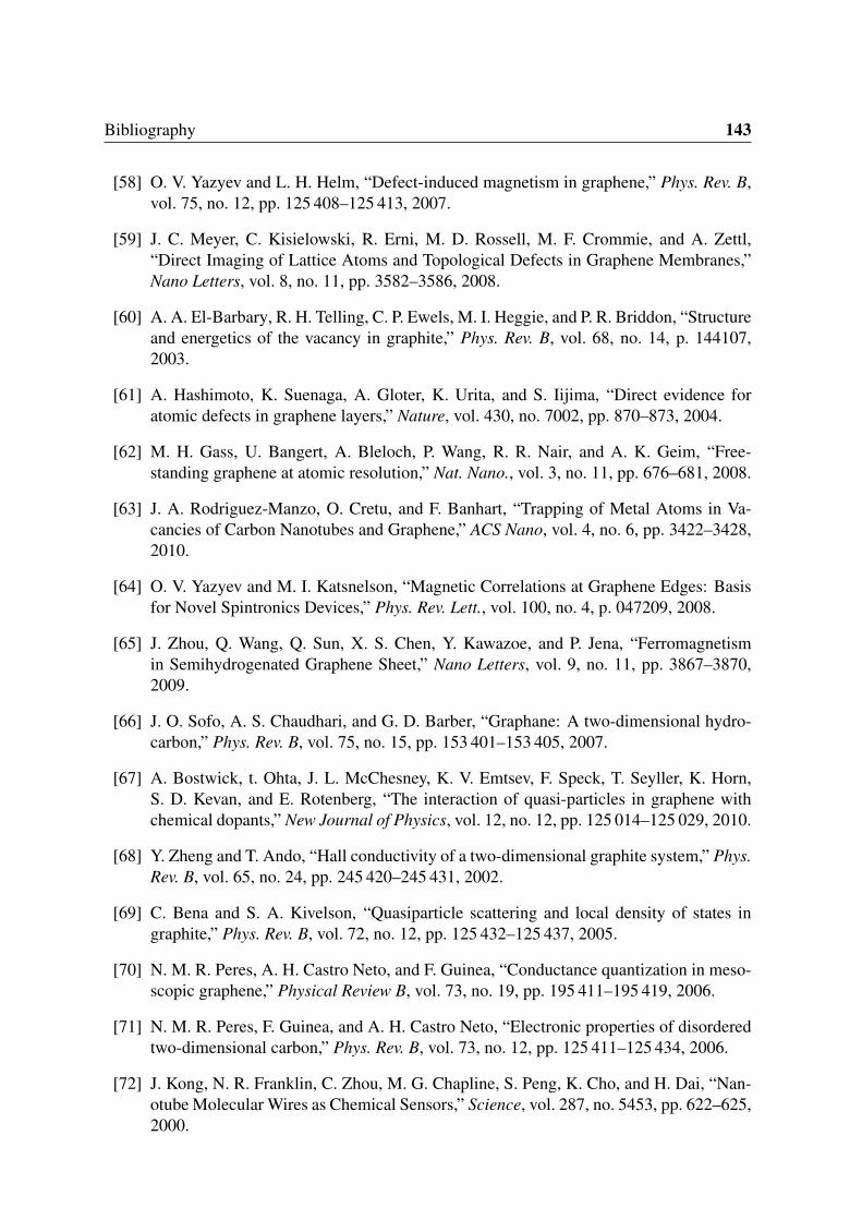
Bibliography 143
[58] O. V. Yazyev and L. H. Helm, “Defect-induced magnetism in graphene,” Phys. Rev. B,vol. 75, no. 12, pp. 125 408–125 413, 2007.
[59] J. C. Meyer, C. Kisielowski, R. Erni, M. D. Rossell, M. F. Crommie, and A. Zettl,“Direct Imaging of Lattice Atoms and Topological Defects in Graphene Membranes,”Nano Letters, vol. 8, no. 11, pp. 3582–3586, 2008.
[60] A. A. El-Barbary, R. H. Telling, C. P. Ewels, M. I. Heggie, and P. R. Briddon, “Structureand energetics of the vacancy in graphite,” Phys. Rev. B, vol. 68, no. 14, p. 144107,2003.
[61] A. Hashimoto, K. Suenaga, A. Gloter, K. Urita, and S. Iijima, “Direct evidence foratomic defects in graphene layers,” Nature, vol. 430, no. 7002, pp. 870–873, 2004.
[62] M. H. Gass, U. Bangert, A. Bleloch, P. Wang, R. R. Nair, and A. K. Geim, “Free-standing graphene at atomic resolution,” Nat. Nano., vol. 3, no. 11, pp. 676–681, 2008.
[63] J. A. Rodriguez-Manzo, O. Cretu, and F. Banhart, “Trapping of Metal Atoms in Va-cancies of Carbon Nanotubes and Graphene,” ACS Nano, vol. 4, no. 6, pp. 3422–3428,2010.
[64] O. V. Yazyev and M. I. Katsnelson, “Magnetic Correlations at Graphene Edges: Basisfor Novel Spintronics Devices,” Phys. Rev. Lett., vol. 100, no. 4, p. 047209, 2008.
[65] J. Zhou, Q. Wang, Q. Sun, X. S. Chen, Y. Kawazoe, and P. Jena, “Ferromagnetismin Semihydrogenated Graphene Sheet,” Nano Letters, vol. 9, no. 11, pp. 3867–3870,2009.
[66] J. O. Sofo, A. S. Chaudhari, and G. D. Barber, “Graphane: A two-dimensional hydro-carbon,” Phys. Rev. B, vol. 75, no. 15, pp. 153 401–153 405, 2007.
[67] A. Bostwick, t. Ohta, J. L. McChesney, K. V. Emtsev, F. Speck, T. Seyller, K. Horn,S. D. Kevan, and E. Rotenberg, “The interaction of quasi-particles in graphene withchemical dopants,” New Journal of Physics, vol. 12, no. 12, pp. 125 014–125 029, 2010.
[68] Y. Zheng and T. Ando, “Hall conductivity of a two-dimensional graphite system,” Phys.Rev. B, vol. 65, no. 24, pp. 245 420–245 431, 2002.
[69] C. Bena and S. A. Kivelson, “Quasiparticle scattering and local density of states ingraphite,” Phys. Rev. B, vol. 72, no. 12, pp. 125 432–125 437, 2005.
[70] N. M. R. Peres, A. H. Castro Neto, and F. Guinea, “Conductance quantization in meso-scopic graphene,” Physical Review B, vol. 73, no. 19, pp. 195 411–195 419, 2006.
[71] N. M. R. Peres, F. Guinea, and A. H. Castro Neto, “Electronic properties of disorderedtwo-dimensional carbon,” Phys. Rev. B, vol. 73, no. 12, pp. 125 411–125 434, 2006.
[72] J. Kong, N. R. Franklin, C. Zhou, M. G. Chapline, S. Peng, K. Cho, and H. Dai, “Nan-otube Molecular Wires as Chemical Sensors,” Science, vol. 287, no. 5453, pp. 622–625,2000.
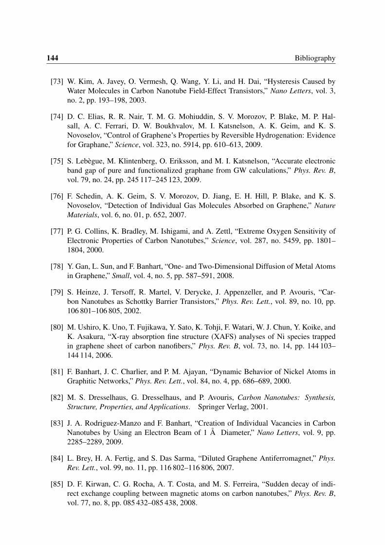
144 Bibliography
[73] W. Kim, A. Javey, O. Vermesh, Q. Wang, Y. Li, and H. Dai, “Hysteresis Caused byWater Molecules in Carbon Nanotube Field-Effect Transistors,” Nano Letters, vol. 3,no. 2, pp. 193–198, 2003.
[74] D. C. Elias, R. R. Nair, T. M. G. Mohiuddin, S. V. Morozov, P. Blake, M. P. Hal-sall, A. C. Ferrari, D. W. Boukhvalov, M. I. Katsnelson, A. K. Geim, and K. S.Novoselov, “Control of Graphene’s Properties by Reversible Hydrogenation: Evidencefor Graphane,” Science, vol. 323, no. 5914, pp. 610–613, 2009.
[75] S. Lebègue, M. Klintenberg, O. Eriksson, and M. I. Katsnelson, “Accurate electronicband gap of pure and functionalized graphane from GW calculations,” Phys. Rev. B,vol. 79, no. 24, pp. 245 117–245 123, 2009.
[76] F. Schedin, A. K. Geim, S. V. Morozov, D. Jiang, E. H. Hill, P. Blake, and K. S.Novoselov, “Detection of Individual Gas Molecules Absorbed on Graphene,” NatureMaterials, vol. 6, no. 01, p. 652, 2007.
[77] P. G. Collins, K. Bradley, M. Ishigami, and A. Zettl, “Extreme Oxygen Sensitivity ofElectronic Properties of Carbon Nanotubes,” Science, vol. 287, no. 5459, pp. 1801–1804, 2000.
[78] Y. Gan, L. Sun, and F. Banhart, “One- and Two-Dimensional Diffusion of Metal Atomsin Graphene,” Small, vol. 4, no. 5, pp. 587–591, 2008.
[79] S. Heinze, J. Tersoff, R. Martel, V. Derycke, J. Appenzeller, and P. Avouris, “Car-bon Nanotubes as Schottky Barrier Transistors,” Phys. Rev. Lett., vol. 89, no. 10, pp.106 801–106 805, 2002.
[80] M. Ushiro, K. Uno, T. Fujikawa, Y. Sato, K. Tohji, F. Watari, W. J. Chun, Y. Koike, andK. Asakura, “X-ray absorption fine structure (XAFS) analyses of Ni species trappedin graphene sheet of carbon nanofibers,” Phys. Rev. B, vol. 73, no. 14, pp. 144 103–144 114, 2006.
[81] F. Banhart, J. C. Charlier, and P. M. Ajayan, “Dynamic Behavior of Nickel Atoms inGraphitic Networks,” Phys. Rev. Lett., vol. 84, no. 4, pp. 686–689, 2000.
[82] M. S. Dresselhaus, G. Dresselhaus, and P. Avouris, Carbon Nanotubes: Synthesis,Structure, Properties, and Applications. Springer Verlag, 2001.
[83] J. A. Rodriguez-Manzo and F. Banhart, “Creation of Individual Vacancies in CarbonNanotubes by Using an Electron Beam of 1 Å Diameter,” Nano Letters, vol. 9, pp.2285–2289, 2009.
[84] L. Brey, H. A. Fertig, and S. Das Sarma, “Diluted Graphene Antiferromagnet,” Phys.Rev. Lett., vol. 99, no. 11, pp. 116 802–116 806, 2007.
[85] D. F. Kirwan, C. G. Rocha, A. T. Costa, and M. S. Ferreira, “Sudden decay of indi-rect exchange coupling between magnetic atoms on carbon nanotubes,” Phys. Rev. B,vol. 77, no. 8, pp. 085 432–085 438, 2008.
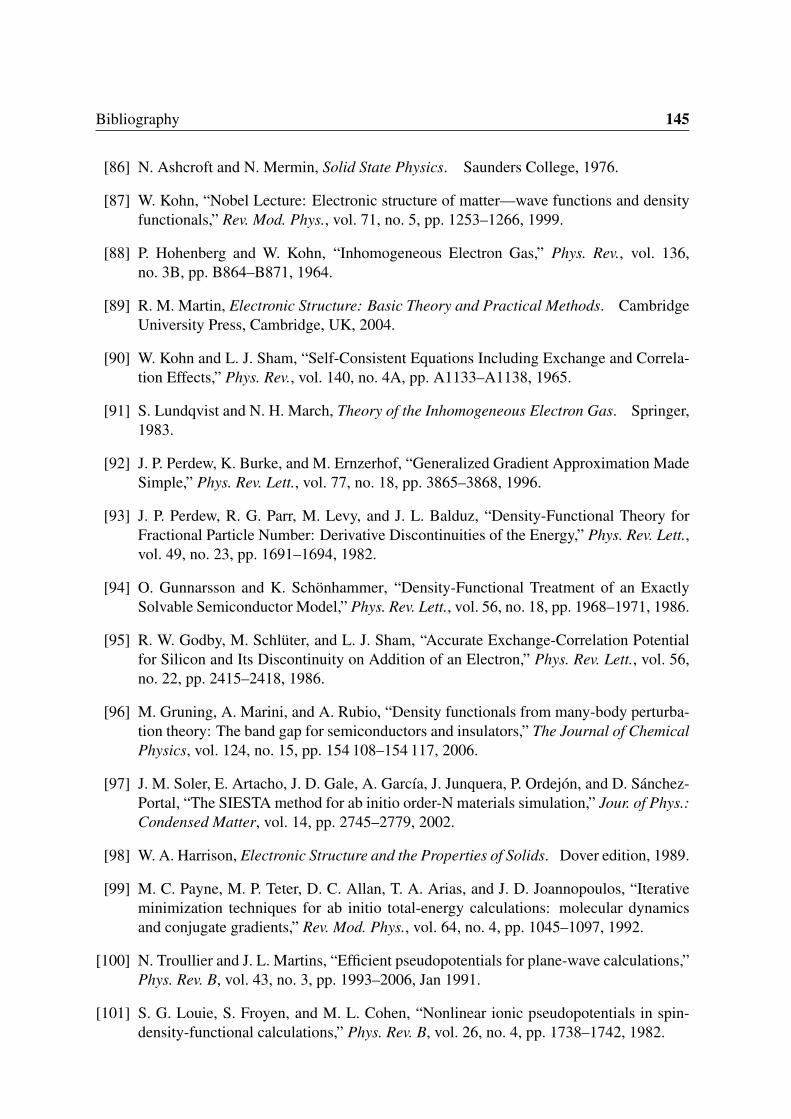
Bibliography 145
[86] N. Ashcroft and N. Mermin, Solid State Physics. Saunders College, 1976.
[87] W. Kohn, “Nobel Lecture: Electronic structure of matter—wave functions and densityfunctionals,” Rev. Mod. Phys., vol. 71, no. 5, pp. 1253–1266, 1999.
[88] P. Hohenberg and W. Kohn, “Inhomogeneous Electron Gas,” Phys. Rev., vol. 136,no. 3B, pp. B864–B871, 1964.
[89] R. M. Martin, Electronic Structure: Basic Theory and Practical Methods. CambridgeUniversity Press, Cambridge, UK, 2004.
[90] W. Kohn and L. J. Sham, “Self-Consistent Equations Including Exchange and Correla-tion Effects,” Phys. Rev., vol. 140, no. 4A, pp. A1133–A1138, 1965.
[91] S. Lundqvist and N. H. March, Theory of the Inhomogeneous Electron Gas. Springer,1983.
[92] J. P. Perdew, K. Burke, and M. Ernzerhof, “Generalized Gradient Approximation MadeSimple,” Phys. Rev. Lett., vol. 77, no. 18, pp. 3865–3868, 1996.
[93] J. P. Perdew, R. G. Parr, M. Levy, and J. L. Balduz, “Density-Functional Theory forFractional Particle Number: Derivative Discontinuities of the Energy,” Phys. Rev. Lett.,vol. 49, no. 23, pp. 1691–1694, 1982.
[94] O. Gunnarsson and K. Schönhammer, “Density-Functional Treatment of an ExactlySolvable Semiconductor Model,” Phys. Rev. Lett., vol. 56, no. 18, pp. 1968–1971, 1986.
[95] R. W. Godby, M. Schlüter, and L. J. Sham, “Accurate Exchange-Correlation Potentialfor Silicon and Its Discontinuity on Addition of an Electron,” Phys. Rev. Lett., vol. 56,no. 22, pp. 2415–2418, 1986.
[96] M. Gruning, A. Marini, and A. Rubio, “Density functionals from many-body perturba-tion theory: The band gap for semiconductors and insulators,” The Journal of ChemicalPhysics, vol. 124, no. 15, pp. 154 108–154 117, 2006.
[97] J. M. Soler, E. Artacho, J. D. Gale, A. García, J. Junquera, P. Ordejón, and D. Sánchez-Portal, “The SIESTA method for ab initio order-N materials simulation,” Jour. of Phys.:Condensed Matter, vol. 14, pp. 2745–2779, 2002.
[98] W. A. Harrison, Electronic Structure and the Properties of Solids. Dover edition, 1989.
[99] M. C. Payne, M. P. Teter, D. C. Allan, T. A. Arias, and J. D. Joannopoulos, “Iterativeminimization techniques for ab initio total-energy calculations: molecular dynamicsand conjugate gradients,” Rev. Mod. Phys., vol. 64, no. 4, pp. 1045–1097, 1992.
[100] N. Troullier and J. L. Martins, “Efficient pseudopotentials for plane-wave calculations,”Phys. Rev. B, vol. 43, no. 3, pp. 1993–2006, Jan 1991.
[101] S. G. Louie, S. Froyen, and M. L. Cohen, “Nonlinear ionic pseudopotentials in spin-density-functional calculations,” Phys. Rev. B, vol. 26, no. 4, pp. 1738–1742, 1982.
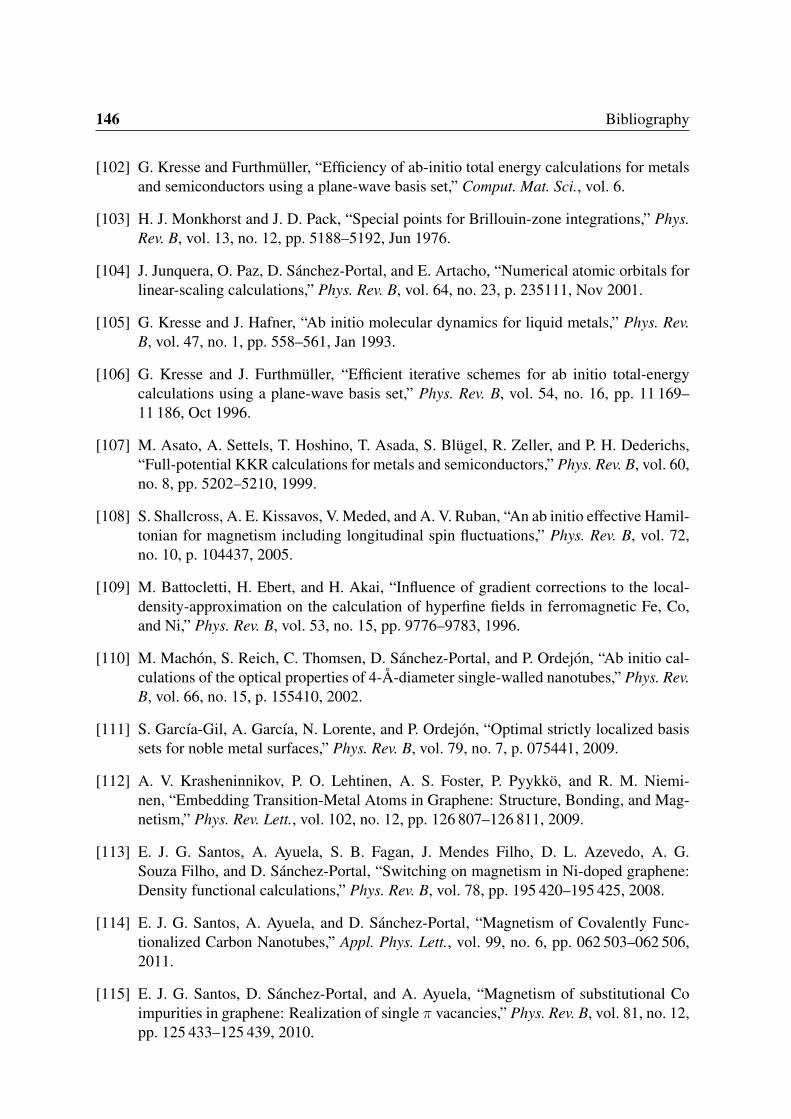
146 Bibliography
[102] G. Kresse and Furthmüller, “Efficiency of ab-initio total energy calculations for metalsand semiconductors using a plane-wave basis set,” Comput. Mat. Sci., vol. 6.
[103] H. J. Monkhorst and J. D. Pack, “Special points for Brillouin-zone integrations,” Phys.Rev. B, vol. 13, no. 12, pp. 5188–5192, Jun 1976.
[104] J. Junquera, O. Paz, D. Sánchez-Portal, and E. Artacho, “Numerical atomic orbitals forlinear-scaling calculations,” Phys. Rev. B, vol. 64, no. 23, p. 235111, Nov 2001.
[105] G. Kresse and J. Hafner, “Ab initio molecular dynamics for liquid metals,” Phys. Rev.B, vol. 47, no. 1, pp. 558–561, Jan 1993.
[106] G. Kresse and J. Furthmüller, “Efficient iterative schemes for ab initio total-energycalculations using a plane-wave basis set,” Phys. Rev. B, vol. 54, no. 16, pp. 11 169–11 186, Oct 1996.
[107] M. Asato, A. Settels, T. Hoshino, T. Asada, S. Blügel, R. Zeller, and P. H. Dederichs,“Full-potential KKR calculations for metals and semiconductors,” Phys. Rev. B, vol. 60,no. 8, pp. 5202–5210, 1999.
[108] S. Shallcross, A. E. Kissavos, V. Meded, and A. V. Ruban, “An ab initio effective Hamil-tonian for magnetism including longitudinal spin fluctuations,” Phys. Rev. B, vol. 72,no. 10, p. 104437, 2005.
[109] M. Battocletti, H. Ebert, and H. Akai, “Influence of gradient corrections to the local-density-approximation on the calculation of hyperfine fields in ferromagnetic Fe, Co,and Ni,” Phys. Rev. B, vol. 53, no. 15, pp. 9776–9783, 1996.
[110] M. Machón, S. Reich, C. Thomsen, D. Sánchez-Portal, and P. Ordejón, “Ab initio cal-culations of the optical properties of 4-Å-diameter single-walled nanotubes,” Phys. Rev.B, vol. 66, no. 15, p. 155410, 2002.
[111] S. García-Gil, A. García, N. Lorente, and P. Ordejón, “Optimal strictly localized basissets for noble metal surfaces,” Phys. Rev. B, vol. 79, no. 7, p. 075441, 2009.
[112] A. V. Krasheninnikov, P. O. Lehtinen, A. S. Foster, P. Pyykkö, and R. M. Niemi-nen, “Embedding Transition-Metal Atoms in Graphene: Structure, Bonding, and Mag-netism,” Phys. Rev. Lett., vol. 102, no. 12, pp. 126 807–126 811, 2009.
[113] E. J. G. Santos, A. Ayuela, S. B. Fagan, J. Mendes Filho, D. L. Azevedo, A. G.Souza Filho, and D. Sánchez-Portal, “Switching on magnetism in Ni-doped graphene:Density functional calculations,” Phys. Rev. B, vol. 78, pp. 195 420–195 425, 2008.
[114] E. J. G. Santos, A. Ayuela, and D. Sánchez-Portal, “Magnetism of Covalently Func-tionalized Carbon Nanotubes,” Appl. Phys. Lett., vol. 99, no. 6, pp. 062 503–062 506,2011.
[115] E. J. G. Santos, D. Sánchez-Portal, and A. Ayuela, “Magnetism of substitutional Coimpurities in graphene: Realization of single π vacancies,” Phys. Rev. B, vol. 81, no. 12,pp. 125 433–125 439, 2010.
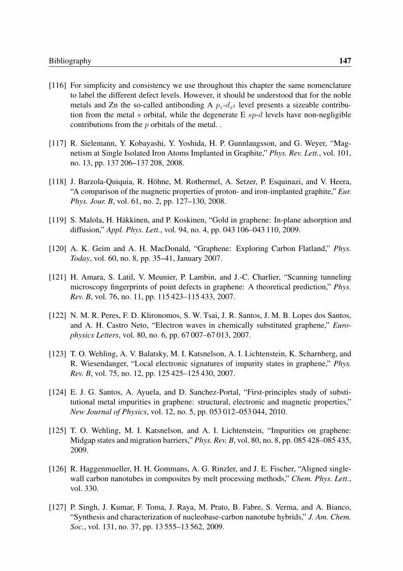
Bibliography 147
[116] For simplicity and consistency we use throughout this chapter the same nomenclatureto label the different defect levels. However, it should be understood that for the noblemetals and Zn the so-called antibonding A pz-dz2 level presents a sizeable contribu-tion from the metal s orbital, while the degenerate E sp-d levels have non-negligiblecontributions from the p orbitals of the metal. .
[117] R. Sielemann, Y. Kobayashi, Y. Yoshida, H. P. Gunnlaugsson, and G. Weyer, “Mag-netism at Single Isolated Iron Atoms Implanted in Graphite,” Phys. Rev. Lett., vol. 101,no. 13, pp. 137 206–137 208, 2008.
[118] J. Barzola-Quiquia, R. Höhne, M. Rothermel, A. Setzer, P. Esquinazi, and V. Heera,“A comparison of the magnetic properties of proton- and iron-implanted graphite,” Eur.Phys. Jour. B, vol. 61, no. 2, pp. 127–130, 2008.
[119] S. Malola, H. Häkkinen, and P. Koskinen, “Gold in graphene: In-plane adsorption anddiffusion,” Appl. Phys. Lett., vol. 94, no. 4, pp. 043 106–043 110, 2009.
[120] A. K. Geim and A. H. MacDonald, “Graphene: Exploring Carbon Flatland,” Phys.Today, vol. 60, no. 8, pp. 35–41, January 2007.
[121] H. Amara, S. Latil, V. Meunier, P. Lambin, and J.-C. Charlier, “Scanning tunnelingmicroscopy fingerprints of point defects in graphene: A theoretical prediction,” Phys.Rev. B, vol. 76, no. 11, pp. 115 423–115 433, 2007.
[122] N. M. R. Peres, F. D. Klironomos, S. W. Tsai, J. R. Santos, J. M. B. Lopes dos Santos,and A. H. Castro Neto, “Electron waves in chemically substituted graphene,” Euro-physics Letters, vol. 80, no. 6, pp. 67 007–67 013, 2007.
[123] T. O. Wehling, A. V. Balatsky, M. I. Katsnelson, A. I. Lichtenstein, K. Scharnberg, andR. Wiesendanger, “Local electronic signatures of impurity states in graphene,” Phys.Rev. B, vol. 75, no. 12, pp. 125 425–125 430, 2007.
[124] E. J. G. Santos, A. Ayuela, and D. Sanchez-Portal, “First-principles study of substi-tutional metal impurities in graphene: structural, electronic and magnetic properties,”New Journal of Physics, vol. 12, no. 5, pp. 053 012–053 044, 2010.
[125] T. O. Wehling, M. I. Katsnelson, and A. I. Lichtenstein, “Impurities on graphene:Midgap states and migration barriers,” Phys. Rev. B, vol. 80, no. 8, pp. 085 428–085 435,2009.
[126] R. Haggenmueller, H. H. Gommans, A. G. Rinzler, and J. E. Fischer, “Aligned single-wall carbon nanotubes in composites by melt processing methods,” Chem. Phys. Lett.,vol. 330.
[127] P. Singh, J. Kumar, F. Toma, J. Raya, M. Prato, B. Fabre, S. Verma, and A. Bianco,“Synthesis and characterization of nucleobase-carbon nanotube hybrids,” J. Am. Chem.Soc., vol. 131, no. 37, pp. 13 555–13 562, 2009.
148 Bibliography
[128] R. K. Saini, I. W. Chiang, H. Peng, R. E. Smalley, W. E. Billups, R. H. Hauge, andJ. L. Margrave, “Covalent sidewall functionalization of single wall carbon nanotubes,”J. Am. Chem. Soc., vol. 125, no. 12, pp. 3617–3621, 2003.
[129] J. L. Bahr, J. Yang, D. V. Kosynkin, M. J. Bronikowski, R. E. Smalley, and J. M.Tour, “Functionalization of Carbon Nanotubes by Electrochemical Reduction of ArylDiazonium Salts:âAL’A Bucky Paper Electrode,” J. Am. Chem. Soc., vol. 123, no. 27,pp. 6536–6542, 2001.
[130] H. A. Mizes and J. S. Foster, “Long-Range Electronic Perturbations Caused by DefectsUsing Scanning Tunneling Microscopy,” Science, vol. 244, no. 4904, pp. 559–562,1989.
[131] G. M. Rutter, J. N. Crain, N. P. Guisinger, T. Li, P. N. First, and J. A. Stroscio, “Scatter-ing and Interference in Epitaxial Graphene,” Science, vol. 317, no. 5835, pp. 219–222,2007.
[132] P. Ruffieux, O. Gröning, P. Schwaller, L. Schlapbach, and P. Gröning, “HydrogenAtoms Cause Long-Range Electronic Effects on Graphite,” Phys. Rev. Lett., vol. 84,no. 21, pp. 4910–4913, 2000.
[133] O. V. Yazyev, “Magnetism in Disordered Graphene and Irradiated Graphite,” Phys. Rev.Lett., vol. 101, no. 3, p. 037203, 2008.
[134] S. Saremi, “RKKY in half-filled bipartite lattices: Graphene as an example,” Phys. Rev.B, vol. 76, no. 18, p. 184430, 2007.
[135] M. A. H. Vozmediano, M. P. López-Sancho, T. Stauber, and F. Guinea, “Local defectsand ferromagnetism in graphene layers,” Phys. Rev. B, vol. 72, no. 15, p. 155121, 2005.
[136] D. W. Boukhvalov, M. I. Katsnelson, and A. I. Lichtenstein, “Hydrogen on graphene:Electronic structure, total energy, structural distortions and magnetism from first-principles calculations,” Phys. Rev. B, vol. 77, no. 3, pp. 035 427–035 434, 2008.
[137] A. V. Shytov, D. A. Abanin, and L. S. Levitov, “Long-Range Interaction betweenAdatoms in Graphene,” Phys. Rev. Lett., vol. 103, no. 1, p. 016806, 2009.
[138] J. Rohrl, M. Hundhausen, K. V. Emtsev, T. Seyller, R. Graupner, and L. Ley, “Ramanspectra of epitaxial graphene on SiC(0001),” Applied Physics Letters, vol. 92, no. 20,pp. 201 918–201 921, 2008.
[139] G. M. Rutter, N. P. Guisinger, J. N. Crain, E. A. A. Jarvis, M. D. Stiles, T. Li, P. N. First,and J. A. Stroscio, “Imaging the interface of epitaxial graphene with silicon carbide viascanning tunneling microscopy,” Phys. Rev. B, vol. 76, no. 23, pp. 235 416–235 422,2007.
[140] A. L. Vázquez de Parga, F. Calleja, B. Borca, M. C. G. Passeggi, J. J. Hinarejos,F. Guinea, and R. Miranda, “Periodically Rippled Graphene: Growth and SpatiallyResolved Electronic Structure,” Phys. Rev. Lett., vol. 100, no. 5, pp. 056 807–056 811,2008.
Bibliography 149
[141] H. C. Schniepp, K. N. Kudin, J. L. Li, R. K. PrudâAZhomme, R. Car, D. A. Saville, andI. A. Aksay, “Bending Properties of Single Functionalized Graphene Sheets Probed byAtomic Force Microscopy,” ACS Nano, vol. 2, no. 12, pp. 2577–2584, 2008.
[142] U. Bangert, M. H. Gass, A. L. Bleloch, R. R. Nair, and A. K. Geim, “Manifestation ofripples in free-standing graphene in lattice images obtained in an aberration-correctedscanning transmission electron microscope,” physica status solidi (a), vol. 206, no. 6,pp. 1117–1122, 2009.
[143] T. M. G. Mohiuddin, A. Lombardo, R. R. Nair, A. Bonetti, G. Savini, R. Jalil, N. Bonini,D. M. Basko, C. Galiotis, N. Marzari, K. S. Novoselov, A. K. Geim, and A. C. Ferrari,“Uniaxial strain in graphene by Raman spectroscopy: G peak splitting, Grüneisen pa-rameters, and sample orientation,” Phys. Rev. B, vol. 79, no. 20, pp. 205 433–205 441,2009.
[144] K. S. Kim, Y. Zhao, H. Jang, S. Y. Lee, J. M. Kim, K. S. Kim, J. H. Ahn, P. Kim, J. Y.Choi, and B. H. Hong, “Large-scale pattern growth of graphene films for stretchabletransparent electrodes,” Nature, vol. 457, no. 7230, pp. 706–710, 2009.
[145] B. Standley, W. Bao, H. Zhang, J. Bruck, C. N. Lau, and M. Bockrath, “Graphene-Based Atomic-Scale Switches,” Nano Letters, vol. 8, no. 10, pp. 3345–3349, 2008.
[146] A. K. Geim, “Graphene: Status and Prospects,” Science, vol. 324, pp. 1530–1534, 2009.
[147] L. Xie, X. Wang, J. Lu, Z. Ni, M. Luo, Z.and Mao, R. Wang, W. Y., H. Huang, D. Qi,R. Liu, T. Yu, Z. Shen, T. Wu, H. Peng, B. Ozyilmaz, K. Loh, A. T. S. Wee, Ariando,and W. Chen, “Room temperature ferromagnetism in partially hydrogenated epitaxialgraphene,” App. Phys. Lett., vol. 98, no. 19, pp. 193 113–193 116, 2011.
[148] E. J. G. Santos, A. Ayuela, D. Sánchez-Portal, and M. Brandbyge, “Gate-Field Con-trolled Spin Transport in Graphitic Carbon,” Submitted.