Embed Size (px)
Citation preview

The NovelThe Novel NanostructuresNanostructuresof Carbonof Carbon
Mildred DresselhausMildred DresselhausMildred DresselhausMildred DresselhausMassachusetts Institute of TechnologyMassachusetts Institute of Technology
Cambridge, MACambridge, MACambridge, MACambridge, MA
University of Tokyo Lecture University of Tokyo Lecture January 30, 2008January 30, 2008
C ll bM.A. Pimenta, UFMG BrazilA. Jorio, UFMG BrazilF. Plentz Filho, UFMG Brazil
Collaborators:G. Dresselhaus, MITA. Tokmakoff, MITS G Chou MIT
M. Endo, Shinshu UR. Saito, Tohoku US. Maruyama, Tokyo U,
A. Souza Filho, UFC BrazilR. Capaz, UFRJ BrazilPaula Corio, USP Brazil
S.G. Chou, MITH. Son, MITJ. Kong, MITM. Hofmann, MIT
S. a uya a, o yo UK. Kaneko, Chiba UY.A. Kim, Shinshu UM. Terrones, IPICYT, Mexico
OutlineOutline
• Overview of graphene and graphite• Carbon Nanotubes as Prototype Materials• Graphene and Graphene RibbonsGraphene and Graphene Ribbons• The Future of Carbon Nanostructures

NanoNano--Science & NanoScience & Nano--TechnologyTechnologygygy
Physicists BiologistsNanoscience
Ch i t Engineers
&Nanotechnology
Chemists Engineers
It’s just the beginning… and it will lead to a revolution in technology with a major impact revolution in technology with a major impact on sience, society and lifestyle, environment and sustainability, medicine…y,

Existing NanotechnologyExisting NanotechnologyNature-made Human-made

Carbon: a remarkable elementCarbon: a remarkable element
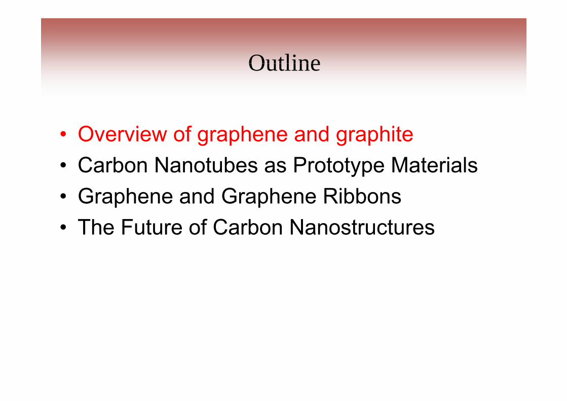
Graphene is the Mother of all nano-Graphitic formsGraphene is the Mother of all nano Graphitic forms
2D
•Graphene is one million times thinner (10-6) than a sheet of paper.G h i 2D b ildi bl k i l f h 2 b d d b
0D 3D1D 1D
•Graphene is a 2D building block material for other sp2 bonded carbon materials. It can be wrapped up into 0D fullerenes, rolled into 1D nanotubes, cut into 1D graphene ribbons or stacked into 3D graphite

The Electronic Structure of Graphene
P.R. Wallace, Phys. Rev. 71, 622 (1947)
Discovered long agoEF
Unique electronic structure
Near the K point
( ) v | |FE κ κ± = ±h linear κ relation
c-c3a a= ⋅03v2F
aγ=
handwhere
(γ0 values are from 2.9 to 3.1eV)is the overlap integral between nearest neighbor π-orbitals 0γand

Magnetoreflection in Graphite
• First magneto-optical experiment to measure energy bands at• First magneto-optical experiment to measure energy bands at several regions of the Brillouin zone(near K and H)
M.S. Dresselhaus and J.G. Mavroides. IBM Journal of Research and Development 8 262 (1964)
• Experiment (1961) was enabled by availability of a new material, highly oriented pyrolytic graphite (HOPG) Ubbelohde (1960)U d t b d E(k) d l b d t i ld d
Research and Development 8, 262 (1964)
• Used symmetry-based E(k) model based on symmetry yielded band parameters for the electronic structure of graphite.
J.W..McClure Phys. Rev, 108, 612 (1957); 119, 606 (1960)

Identification of Electrons and Holes in Graphite
Using circular polarized radiation in the first magneto-optical experiment using a laser, the locations of electrons and holes in the Brillouin zone were identified
P.R.Schroeder, M.S. Dresselhaus and A.Javan, Phys.Rev. Lett 20,1292 (1968)
The locations of electrons and holes are incorrectly given in theThe locations of electrons and holes are incorrectly given in the literature, prior to 1968.

Spintronics in Graphene• Building on an early paper by Gene Dresselhaus on what in
now known as the “Dresselhaus spin-orbit term” in III-Vnow known as the Dresselhaus spin orbit term in III V semiconductors {G. Dresselhaus, Phys. Rev. 71, 220 (1955)} a model for the spin-orbit interaction in graphite as imposed by symmetry was developed {G Dresselhaus Phys Rev 140symmetry was developed {G. Dresselhaus, Phys. Rev. 140, A401 (1965)}
• Since the spin-orbit interaction in graphite is very small, the spin lifetime in graphene can be very long. Therefore graphene has become an interesting material for studying spin transport.

Entry into the Nanoworld
• Through the unexpected observation by Hannay et al. at AT&T Bell Labs of superconductivity in stage 1 graphite intercalation compounds (C8K)
Hannay et al, Phys.Rev.Lett. 14, 225 (1965)
• Much interest was aroused since neither potassium nor carbon isneither potassium nor carbon is superconducting
• Intercalation compounds allowed early• Intercalation compounds allowed early studies to be made of individual or few graphene layers in the environment of C Kgraphene layers in the environment of the intercalant species. My entry (1973)
C8K

Low Dimensional Science Studies in Graphite Intercalation CompoundsIntercalation Compounds
Studies carried out 1973-1992Magnetoreflectiong
TransportRamanRamanOptical
StructuralMagnetic
on single or few layer Graphene in the environment of the intercalant species. C8K

Concurrent Studies on Forerunners to Fullerenes
• Liquid carbon studies (1983)Cx
Laser
Liquid carbon was found to be metallicT. Venkatesan et al, Phys. Rev. Lett. 53, 360 (1984)
Laser
graphite
• The Laser ablation process used to make liquid carbon produced large particle emissions (like C100) rather than C2 or
liquid carbongraphite
C3
• Trip to Exxon Research Lab to di ldiscuss results.
• Soon Exxon published famous paper
E A R hlfi D M C d A K ld JE.A.Rohlfing, D.M. Cox and A.Kaldor. J. Chem.Phys., 81, 332 (1984)

Forerunners of Carbon Nanotubes
• Vapor grown carbon fibersVapor grown carbon fibers• At center of carbon fibers is a multiwall carbon nanotube• Connection of fullerene was made by going fromConnection of fullerene was made by going from
C60 C70 C80
• This idea suggested that a single wall Carbon nanotube would gg gbe interesting (August 1991) and led to calculating the electronic structure of SWNTs before they were ever seen
• Theoretical works stimlated synthesis of SWNTs
M.S.Dresselhaus et al., Graphite Fibers and Filaments, Springer (1988)

Unique One Dimensional (1D) Properties
Carbon nanotubes and nanoribbons
• High aspect ratio have:
• Enhanced density of states in 1D• Molecular behavior (spikes in DOS)• Solid state behavior (tails in DOS)
. O. S
.
. O. S
.
O. S
.
. O. S
.
3D 2D 1D 0D
E
D D D. D
E E E
3DBulk Semiconductor
2DQuantum Well
1DQuantum Wire
0DQuantum Dot

General Relations between 1D and 2D Systems shown in terms of carbon nanotubesshown in terms of carbon nanotubes
Rolling up a 2D sheet Confinement of 1D electronic stateson cutting lineson cutting lines
1D2D
1D van Hove singularities ggive high density of
electronic states (DOS) at well defined energies
Carbon nanotubes are metallic if cutting line passes through the K point

Unique Properties of Carbon NanotubesUnique Properties of Carbon Nanotubeswithin the Nanoworldwithin the Nanoworldwithin the Nanoworldwithin the Nanoworld
• Small size: ~1 nm diameter (down to ~10 atoms around the circumference)
graphene ribbon SWNT
• Electronic Properties: can be eithermetallic or semiconducting depending on diameter and orientation of the
armchair
hexagons
• Mechanical: Very high strength, d l d ili
zigzagmodulus, and resiliency.
• Physics: model system for1D density f l t i t t
g g
of electronic states.
• Single molecule Raman spectroscopy, luminescence and transport properties
chiral
luminescence and transport properties.

Unique Properties of Graphene NanoribbonsZigzag •A special feature of graphene ribbons is
their long edges with narrow widths
•The crystallographic orientation of the edges strongly influences their electronic
Armchair
edges strongly influences their electronic and other properties.
fArmchair •Zigzag ribbons show a high density of states at EF and are zero gap semiconductors.semiconductors.
•Armchair edge ribbons (like single wall b t b ) b ith t llicarbon nanotubes) can be either metallic
(N=3M-1) or semiconducting (N=3M, N=3M+1), where N,M are integers), , g
N=number of hexagon columns along the ribbon width.

Potential Applications of Carbon NanotubesMore emphasis now is on applications
ppChapter by M. Endo, M. S. Strano, P. M. Ajayan @ Springer TAP111
Large Volume Applications Limited Volume Applications(Mostly based on Engineered Nanotube Structures)
Present - Battery Electrode Additives (MWNT)- Composites (sporting goods; MWNT)-Composites (ESD* applications; MWNT)
- Scanning Probe Tips (MWNT)- Specialized Medical Appliances (catheters) (MWNT)
-(*ESD – Electrical Shielding Device)
Near Term(less than ten
)
- Battery and Super-capacitor Electrodes- Multifunctional Composites - Fuel Cell Electrodes (catalyst support)
- Single Tip Electron Guns- Multi-Tip Array X-ray Sources- Probe Array Test Systemsyears) Fuel Cell Electrodes (catalyst support)
- Transparent Conducting Films- Field Emission Displays / Lighting- CNT based Inks for Printing
Probe Array Test Systems- CNT Brush Contacts- CNT Sensor Devices- Electro-mechanical Memory Device- Thermal Management SystemsThermal Management Systems
Long Term(beyond ten years)
- Power Transmission Cables- Structural Composites (aerospace and automobile etc.)
CNTs in Photovoltaic Devices
- Nano-electronics (FET,Interconnects)- Flexible Electronics- CNT based bio-sensors
CNT Fitration/Separation Membranes- CNTs in Photovoltaic Devices - CNT Fitration/Separation Membranes- Drug-delivery Systems

OutlineOutline
• Overview of graphene and graphite• Carbon Nanotubes as Prototype Materials• Graphene and Graphene RibbonsGraphene and Graphene Ribbons• The Future of Carbon Nanostructures

Nanotube Structure in a Nutshell
(4,2)
Graphene Sheet SWNT
Rolled-up graphene layerLarge unit cell.
2 2
( )t
L ad n nm mC na ma n m π π
⎧ = = + +⎪⎪= + ≡ ⎨r r r
1 21
( , )3tan
2
hC na ma n mm
n mθ −
= + ≡ ⎨⎪ =⎪ +⎩
Each (n,m) nanotube is a unique moleculeR.Saito et al, Imperial College Press, 1998

Resonance Raman Spectroscopy (RRS)Resonance Raman Spectroscopy (RRS)A.M. Rao et al., Science 275 (1997) 187A.M. Rao et al., Science 275 (1997) 187
RRS: R.C.C. Leite & S.P.S. Porto, PRL 17, 10-12 (1966)
Raman spectra from SWNT bundles• Enhanced Signal
Optical AbsorptionOptical Absorptione-DOS peaks
Trigonal warping effect
E = 0.94eV
= 1 17eV= 1.17eV
= 1.58eVπ π∗
= 1.92eV
= 2 41eV
diameter-selective resonance processωRBM = α /dt
Confirms: 2.41eVConfirms:•Resonant density of states (DOS)•Each (n,m) tube has different spectrum

Single Nanotube Spectroscopy yields ESingle Nanotube Spectroscopy yields Eiiii, (, (n,mn,m))
Therefore the geometrical structure of an individual carbon nanotube can be found by spectroscopycarbon nanotube can be found by spectroscopy
A. Jorio (UFMG) et al., Phys. Rev. Lett. 86, 1118 (2001)enabled by a collaboration with C.M.Lieber at HarvardRBMRBM
'
SemiconductingMetallic Each nanotube has a
unique DOS because of trigonal warping effects
R. Saito et al.,Phys. Rev. B 61, 2981 (2000)
R i l fR i l f SWNTSWNTRaman signal from Raman signal from one one SWNTSWNTindicates a strong resonance processindicates a strong resonance process
(ωRBM, Eii)(n,m)

Raman Spectra of SWNT BundlesRaman Spectra of SWNT BundlesMetallic G-band
G-G-band
ity
G+
GG band
an In
tens
i
G+
G-
Ram
a
RBM: ωRBM∝ 1/dt D-band
GG’-band
oRaman Shift (cm−1)
o•RBM gives tube diameter and diameter distribution•Raman D-band characterizes structural disorder•G- band distinguished M, S tubes and G+ relates to charge transfer•G’ band (2nd order of D-band) provides connection of phonon to its wave vector•Each feature in the Raman spectra provides complementary information about nanotubes

Water, 1.1 g/cm3
SDS Band Gap FluorescenceBand Gap FluorescenceM. J. O’Connell M. J. O’Connell et alet al., Science 297 (2002) 593., Science 297 (2002) 593S M B hilS M B hil ll S i 298 (2002) 2361S i 298 (2002) 2361
1.0 g/cm3
1.2 g/cm3
S. M. Bachilo S. M. Bachilo et al., et al., Science 298 (2002) 2361.Science 298 (2002) 2361.
1.2 g/cm
SDS=Sodium Dodecyl Sulfate n (n
m)
2
y
cita
tion
V] c1
c2E
xc Peaks only
0
Ene
rgy
[eV
absorptionfluorescence
v1
c1
E i i ( )v2
G d th d t d t i th ( )
Emission (nm)
0–2Density of Electronic States
e-DOS of (n, m) = (10,5)
Good method to determine the (n,m) semiconducting nanotubes in a sample

Photoluminescence
S. M. Bachilo et al., Science 298, 2361 (2002)
From SDS-wrapped HiPco nanotubes in solution
2n+m=constant family patterns are observed in the PL excitation-emission spectraIdentification of ratio problemShowed value of mapping optical transitions
●Since each peak in the PL map is for a different (n,m) tube, such maps can identify the (n,m) tubes present in the sample.

Extended tight binding modelKataura plot is calculated within theextended tight-binding approximation
curvature effects (ssσ, spσ, ppσ, ppπ)long range interactions (up to ~4Å)
Using the Popov/Porezag approach:
V) long-range interactions (up to ~4Å)
geometrical structure optimization
nerg
y (e
V
The extended tight-bindingcalculations show family behavior(diff ti ti b t S1 & S2an
sitio
n E
(differentiation between S1 & S2and strong chirality dependence)similar to experiments
Tra
I Di t (1/ )Family behavior is strongly influenced by the trigonal warping effect
M 2n+m=3pS1 2n+m=3p+1S2 2n+m=3p+2
Inverse Diameter (1/nm)
p
Ge.G. Samsonidze et al., APL 85, 5703 (2004)N.V. Popov et al Nano Lett. 4, 1795 (2004) & New J. Phys. 6, 17 (2004)

Experimental Justification for excitons
Excitons in Carbon Nanotubes
2-photon excitation to a 2A+ symmetry exciton (2p) and 1-photon emission from a 1A− exciton (1s)
Experimental Justification for excitons
and 1 photon emission from a 1A exciton (1s) cannot be explained by the free electron model
BAND EDGEE (2p)2A+BAND-EDGE
E11 (1s)1A−E11 (2p)
(9,1)E11 (1s) 1.4
GY
1A−
TIO
N (a
.u.)
(6,5)
(8,3)1.3
SIO
N E
NE
RG
AB
SO
RP
T
(7,5)1.2`
1.2 1.4 1.6 1.8
EM
ISS
2-PHOTON EXCITATION ENERGY1.2 1.4 1.6 1.8 2.0
The observation that excitation and emission are
Wang et al. Science 308, 838 (2005)
2-PHOTON EXCITATION ENERGYat different frequencies supports exciton model

Emission Identified withEmission Identified withOne and Two Phonon assisted PL Processes:One and Two Phonon assisted PL Processes:One and Two Phonon assisted PL Processes:One and Two Phonon assisted PL Processes:
Phonon dispersion relationsof graphite
2 iLO/iTO near Γ
2 iTO near K (G’ band)
2 iLO/iLA near K
2 oTO near Γ(M-band)
1iLO/iTO near Γ (G-band)
Two phononprocess
One phononprocessChou et al., PRL 94, 127402 (2005)

NonNon--degenerate Pumpdegenerate Pump--probeprobe
Frequency domain Fast optics, Time domainS G Chou et al PRL 94 127402 (2005)
Epump = 1.57±0.01eV, ~E11(6,5)+2ħωDEprobe = around E11of (6,5) nanotube(Instrument resolution ~250fs)
S. G. Chou et al. PRL 94 127402 (2005)
( )
Intraband l ti
EPump ~E11(6,5)+ 2ħωph, D
Epro
relaxation
Pump
obe =E11(6,
Probe
Pump,5)Interband relaxationrelaxation
S. G. Chou, M.F. DeCamp, A. Tokmakoff, et al. Phys. Rev. B 72, 195415 (2005)
●Fast optics gives information about the dynamics of each phonon assisted transition

Approaches to Carbon DWNTs
• simplest assumptionsimplest assumption
=+ =+
Suggests using electronic E(k) for SWNTs as a first approximation for DWNTs, but E(k) of monolayer and bilayer graphene say more detail is needed
• Carbon DWNTs relate to bilayer graphene

Br2-doped double-wall nanotubes
Br2-DWNTsPristine DWNTs
(a) (b)
Highly pure samples(99% of DWNTs +(a) (b)
TEM images
(99% of DWNTs + 1% of SWNTs + catalystsparticles)
5 nm
5 nm
(c) (d)
SEM images
100nm100nmEndo et al. Nanolett.4,1451 (2004)

Charge transfer and screening effects
(a)
E( )
Inte
nsity
Elaser
2.33 eV M SG band Raman spectra ofBr doped DWNTs
El(b)
Br2 doped Pristine
Ram
an
x0.3
Br2 doped DWNTs.
nten
sity
Elaser
1.58 eV MS
( )
1450 1500 1550 1600 1650Frequency (cm-1)
Ram
an In
q y ( )
Metallic inner tubes highlyaffected by doping
1450 1500 1550 1600 1650R
Frequency (cm-1)
affected by doping
Semiconducting inner tubes are not much affected by doping Frequency (cm )are not much affected by dopingwhen shielded by metallic tubes

Calculated electronic charge density difference (ρ - ρ ) of DWNTs(ρdoped - ρundoped) of DWNTs
Calculation supports experimental observations about charge transfer
A.G. Souza Filho et al Nano Letters (2007)

Undoping experiments on bromine doped DWNTs
Outer tubesBr2
Br2-adsorbed DWNTs
Elaser=2.33 eVEnergy neededfor removingOuter tubes
Br2
tyInner tubes
for removing Br2is ~ 25 meV
Inte
nsit
atin
g
21 oC
Ram
an hea
600 oC
cool
ing
100 200 300 400 50021 oC
F ( -1)Frequency (cm 1)• The dopant is completely removed after heat treatment
Souza Filho et al, PRB (2006)

Spectrum for RBM for pristine and H2SO4doped DWNTsdoped DWNTs
Inner Walls
Outer Walls M
E =2 052 eV H2SO4 doped Pristine
ityElaser=2.052 eV
S
man
Inte
nsR
am
150 200 250 300 350 400
Frequency (cm-1)•Outer semiconducting walls strongly affected by doping•Inner semiconducting (S) tubes weakly interact with dopantInner semiconducting (S) tubes weakly interact with dopant•Inner metallic (M) tubes more strongly interact with dopant
E. Barros et al, PRB (2007)

Summary on Nanotubes
• Because of trigonal warping effects, each g p g ,(n,m) nanotube has a unique geometry which can be distinguished spectroscopically.Th H i l iti i th l t i• The van Hove singularities in the electronic density of states allow single nanotube spectroscopyspectroscopy
• Excitonic effects dominate optical spectra in 1D systems.y
• Double wall nanotubes show that the properties of the individual constituents are
difi d th h h t f i t timodified through charge transfer interactions• DWNT spectra have implications on bilayer
graphenegraphene

OutlineOutline
• Overview of graphene and graphite• Carbon Nanotubes as Prototype Materials• Graphene and Graphene RibbonsGraphene and Graphene Ribbons• The Future of Carbon Nanostructures

Graphene discoveryGraphene discovery( Th S t h t t i k!)( Th S t h t t i k!)(or The Scotch tape trick!)(or The Scotch tape trick!)
++ ==
2.5x 50x
Few Layers
Bulk Graphite
Monolayer
Bilayer
y200x
(2004)

Graphene Crystals
One atom thick single crystals
a) Graphene visualized by an atomic force microscope
b) Graphene sheet freely suspended over posts
c) Scanning electronc) Scanning electron micrograph of a relatively large graphene crystal h i h i dshowing armchair and
zigzag edges. The edges of graphene crystals are of special importance because they are unique to few layer graphenes and y g pgraphene ribbons
adapted from A. Geim

Graphene: the amazing Graphene: the amazing t i lt i lnanomaterialnanomaterial
Thi t t i l h t i i bl t th t t!Thinnest material sheet imaginable…yet the strongest! (5 times stronger than steel and much lighter!)
Graphene is a semimetal: it conducts as good (in fact better!) than the best metals, yet its electrical properties ) , y p pcan be modulated (it can be switched ON and “OFF”)
Hi h bilit ( 10000 2/V @RT) B lli tiHigh mobility (≥10000 cm2/Vs @RT) ⇒ Ballistic conduction for hundreds of nanometers
Superb heat conductor
Very high current densities (~109 A/cm2)

Electronic structure of Monolayer yGraphene
• E(k) relation is linear in k( )• Effective mass vanishes at K and K'• Common metals and semiconductors
which have parabolic E(k) dispersionwhich have parabolic E(k) dispersion relations

Electronic Band Structure of Monolayer and of AB-stacked bilayer Graphene
(a) Monolayer graphene with linear E(k) near the K point at EF(b) Bilayer AB stacked graphene E(k). The weak interaction between
layers introduces a minigap at the K point and parabolic bandslayers introduces a minigap at the K point and parabolic bandsLatil, Phys. Rev. Lett. 97, 036803 (2006)Saito, Phys. Rev. B 33, 7218 (1986)

Ambipolar Electric Field Effectp
Ambipolar electric field effect in single-layer graphene arising from the symmetry between valence and conduction bands. The i t h th l t E(k) th F i l l iinsets show the low-energy spectrum E(k) as the Fermi level is raised by increasing the gate voltage Vg
from A. Geim

Minimum Conductivity of Graphene
The conductivity for different graphene samples indicates that the minimum conductivity is 4e2/hindicates that the minimum conductivity is 4e2/h, rather than 2e2/h as in typical semiconductors

Anomalous Quantum Hall Effect in 1ML GrapheneThree anomalies: • Half integer quantum Hall effect, • Factor of 4 in 4e2/h • Berry’s phase of π
• This work attracted great attention and interest in grapheneZhang et al., Nature 438 (7065) 2005

And shortly after that …And shortly after that …
Nature 438, 197 (2005)
N 438 201 (2005)Nature 438, 201 (2005)
Graphene madness…More than 400 articles inMore than 400 articles in
the past year… (less than 10% are experimental)

Fundamental ScienceFundamental Science
Nature 438, 197 (2005)
N 438 201 (2005)Nature 438, 201 (2005)
Electrons in graphene behave as ultrarelativisticElectrons in graphene behave as ultrarelativisticparticles, despite the fact that they move “slowly”.In other words, they behave as massless particlesy pthat obey the Dirac equation.
“Massless” particlesMassless particlesPhotons Neutrinos
Charge 0 Charge 0Electrons in graphene
Charge (-)Charge 0Spin 0
Charge 0Spin 1/2
Charge ( )Spin 1/2

Fundamental ScienceFundamental ScienceStability of 2-D crystals Relativity + superconductivity
Electronic metamaterialsHeersche et al. Nature 07
Meyer et al. Nature 07
Electronic metamaterials
Falko et al. Science 07

Raman spectra distinguishesof graphene and graphiteELaser=2.41eV
G’GG’
G’
G’A
G’B
•Large enhancement of G’ band in monolayer graphene relative to graphite•G’ band in monolayer graphene (and SWNTs) is a single peak, but the G’ G ba d o o aye g ap e e (a d S s) s a s g e pea , bu e Gband for graphite has two components
J.C. Charlier, P. C. Eklund, J. Zhu and A. C. Ferrari, vol III, TAP, Springer

G' peak distinguishes number of graphene layers
G’1B G’1A G’2A G’2B
Lineshape isLineshape is sensitive to both ELaser and number of layers
The lineshape of G’ band identifies the number of layersThe relative intensities of the 4 peaks distinguishes bilayer graphene from DWNTs
J.C. Charlier, P. C. Eklund, J. Zhu and A. C. Ferrari, vol III, TAP, Springer

Dispersion of wG’ with El for 1LG and 2LGDispersion of wG’ with Elaser for 1LG and 2LG
• dωG’/dElaser ~ 100 cm-1/eV for G′ bandG laser
• Phonon dispersion gives interaction between atoms in plane and across planebetween atoms in-plane and across plane
L. Malard, M. Pimenta (NT07)

Graphene RibbonsArmchairZigzag
•Special feature of graphene ribbons is that they have edges and few columns of hexagons along the width.

Electronic structure of graphene ribbons
Armchair Zigzag Van Hove singularities in the DOS
Metallic for N=3M 1 (M integer)Metallic for N=3M-1 (M integer)
Examples:Metallic for N=5
• Always metallic•Presence of localized
edge states at the Fermi level
and Semiconducting for N=4, 6Fermi level
Nakada et al., Phys. Rev. B 54, 17954 (1996).

Synthesis of Nanographenes from Nanodiamond
• STM images of nanographenes after heat treatment of nano-diamond particles at 1600°C. Magnified image on right
• Some nanographene particles take the shape of ribbons
Affoune et al., Chem. Phys. Lett. 348, 17 (2001), Langmuir 17, 547 (2001) .

Graphene ribbon edges favor armchair and zigzag edge segmentszigzag edge segments
• Armchair edges are the most favored (more stable)Armchair edges are the most favored (more stable)• Higher intensity AFM signal along zigzag edge Z1 supports a high
DOS along zigzag edge Enoki 2007

Characterization of Graphene RibbonsSTM image of a zigzag ribbon:
AFM image of a monolayer graphene ribbon:
AFM image of many nanographite ribbons parallel to each other:parallel to each other:
Cançado et al Phys Rev Lett 93 047403 (2004)
• Laser heating effect allows distinction to be made between the 1D graphene ribbon and 3D graphite substrate.
Cançado et al., Phys. Rev. Lett. 93, 047403 (2004).
bbo a d 3 g ap te subst ate.• Raman polarization spectra allow study of the dependence of the graphene ribbon intensity on polarization angle

Raman spectra of graphene ribbons
G nanographite ribbon
Cançado et al., Phys. Rev. Lett. 93, 047403 (2004).
G1 - nanographite ribbonG2 – 3D graphite substrate
Gruneis et al., Phys. Rev. B 67, 165402 (2003).

Raman and Scanning Probe Microscopy studies on graphene edgesstudies on graphene edges
armchair edgeedge
zigzag edge
• The D-band intensity depends on the edge type:
edge
The D band intensity depends on the edge type: large for armchair edge, smaller for zigzag edge.• But D'-band intensity is similar for zigzag and armchairBut D -band intensity is similar for zigzag and armchair edges

Double resonance Raman scattering in graphite edges
• The defect associated
graphite edges
• The defect associated with the step edge is only able to transfer momentum in the direction perpendicular to th d ( h i )the edge (armchair).
• Raman spectroscopy can be used to distinguish between armchair and zig zag edgeszig-zag edges.
L G C d t l Ph RL. G. Cançado, et al. Phys. Rev. Letters, vol. 93, 247401 (2004)

Potential ApplicationsPotential Applications
NanoelectronicsNanomechanics:Resonators and membranesResonators and membranes
Bunch et al.Science (07)Han et al. PRL (07)
Nanosensing:Ultimate gas sensor?
Schedin et al. Nature Mat. (07)

Challenges AheadChallenges AheadResearch:
Better quality size OKIndustry:
Larger size quality OKBetter quality…size OK Larger size…quality OK
Atomically controlled edges

OutlineOutline
• Overview of graphene and graphite• Carbon Nanotubes as Prototype Materials• Graphene and Graphene RibbonsGraphene and Graphene Ribbons• The Future of Carbon Nanostructures

OutlookOutlook
• 1D carbon nanotubes continue to be an expanding fi ld f i h il li tifield, now focusing more heavily on applications
• 1D carbon nanoribbons is a newly emerging field that is expected to grow rapidly in the near future.
• The synergy between nanotubes, graphene and nanoribbons will surely enrich one another strongly in advancing both their nanoscience and applications.
END


![Synthesis of novel carbon nanostructures through the ...scientiairanica.sharif.edu/article_3473_0c62691b557749a3ab7c2060… · methods: arc discharge [1], laser ablation [3], chemical](https://img.pdfslide.us/doc/110x75/601eb0fb7c462579672452d7/synthesis-of-novel-carbon-nanostructures-through-the-methods-arc-discharge.jpg)