Embed Size (px)
Citation preview

ECE 410, Prof. A. Mason Lecture Notes 6.1
Intrinsic Silicon Properties• Read textbook, section 3.2.1, 3.2.2, 3.2.3
• Intrinsic Semiconductors– undoped (i.e., not n+ or p+) silicon has intrinsic charge
carriers– electron-hole pairs are created by thermal energy– intrinsic carrier concentration ≡ ni = 1.45x1010 cm-3,
at room temp.– function of temperature: increase or decrease with temp?– n = p = ni, in intrinsic (undoped) material
• n ≡ number of electrons, p ≡ number of holes– mass-action law, np = ni
2
• applies to undoped and doped material

ECE 410, Prof. A. Mason Lecture Notes 6.2
Extrinsic Silicon Properties• doping, adding dopants to modify material properties
– n-type = n+, add elements with extra an electron• (arsenic, As, or phosphorus, P), Group V elements• nn ≡ concentration of electrons in n-type material• nn = Nd cm-3, Nd ≡ concentration of donor atoms• pn ≡ concentration of holes in n-type material• Nd pn = ni
2, using mass-action law– always a lot more n than p in n-type material
– p-type = p+, add elements with an extra hole• (boron, B)• pp ≡ concentration of holes in p-type material• pp = Na cm-3, Na ≡ concentration of acceptor atoms• np ≡ concentration of electrons in p-type material• Na np = ni
2, using mass-action law– always a lot more p than n in p-type material
– if both Nd and Na present, nn = Nd-Na, pp=Na-Nddo example on board
ni2 = 2.1x10²⁰
n+/p+ defines regionas heavily doped,
typically ≈ 1016-1018 cm-3
less highly doped regions generally labeled n/p
(without the +)
P P ++
-
group Velement ion
electron
n-type Donor
freecarrier
B B + +-
group IIIelement
hole
p-type Acceptor
ion freecarrier

ECE 410, Prof. A. Mason Lecture Notes 6.3
Conduction in Semiconductors• doping provides free charge carriers, alters conductivity • conductivity, σ, in semic. w/ carrier densities n and p
– σ = q(μnn + μpp), q ≡ electron charge, q = 1.6x10⁻¹⁹ [Coulombs]• μ ≡ mobility [cm2/V-sec], μn ≅ 1360, μp ≅ 480 (typical values)
• in n-type region, nn >> pn– σ ≈ qμnnn
• in p-type region, pp >> np
– σ ≈ qμpnp
• resistivity, ρ = 1/σ• resistance of an n+ or p+ region
– R = ρ l , A = wt
• drift current (flow of charge carriers in presence of an electric field, Ex)– n/p drift current density: Jxn = σn Ex = qμnnnEx, Jxp = σp Ex = qμpppEx
– total drift current density in x direction Jx = q(μnn + μpp) Ex = σ Ex
mobility = average velocity per unit electric field
μn > μpelectrons more mobile than holes
⇒conductivity of n+ > p+
l
t
wA
Mobility often assumed constant
but is a function of Temperature and Doping
Concentration
ECE 410, Prof. A. Mason Lecture Notes 6.4
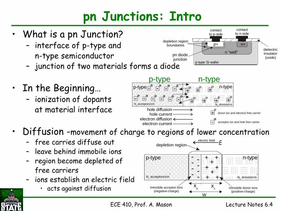
pn Junctions: Intro• What is a pn Junction?
– interface of p-type andn-type semiconductor
– junction of two materials forms a diode
• In the Beginning…– ionization of dopants
at material interface
• Diffusion -movement of charge to regions of lower concentration– free carries diffuse out– leave behind immobile ions– region become depleted of
free carriers– ions establish an electric field
• acts against diffusion
donor ion and electron free carrier
acceptor ion and hole free carrier
p-type
hole diffusionhole current
electron diffusionelectron current
N acceptors/cmA
3
N donors/cmD
3
n-type
-+
-+-+
-+-+
-+
-+-+
+-
+-+-+-+-+-+-
+-+-+-+-
Edepletion region
immobile acceptor ions(negative-charge)
immobile donor ions(positive-charge)
electric field
xp
W
xn
----
----
+++
+++
++
p-type
N acceptors/cmA
3
N donors/cmD
3
n-type
p-type Si wafer
pn diodejunction
depletion regionboundaries
dielectricinsulato(oxide)
contactto p-side
contactto n-side
p+ n+
n “well” r
p-type n-type

ECE 410, Prof. A. Mason Lecture Notes 6.5
pn Junctions: Equilibrium Conditions• Depletion Region
– area at pn interface void of free charges
– charge neutrality• must have equal charge on both sides• q A xp NA = q A xn ND , A=junction area; xp, xn depth into p/n side• ⇒ xp NA = xn ND• depletion region will extend further into the more lightly doped side
of the junction
• Built-in Potential– diffusion of carriers leaves behind immobile charged ions– ions create an electric field which generates a built-in potential
• where VT = kT/q = 26mV at room temperature
Edepletion region
immobile acceptor ions(negative-charge)
immobile donor ions(positive-charge)
electric field
xp
W
xn
----
----
+++
+++
++
p-type
N acceptors/cmA
3
N donors/cmD
3
n-type
NA ND
⎟⎟⎠
⎞⎜⎜⎝
⎛=Ψ 20 ln
i
DAT n
NNV

ECE 410, Prof. A. Mason Lecture Notes 6.6
pn Junctions: Depletion Width• Depletion Width
use Poisson’s equation & charge neutrality– W = xp + xn
• where VR is applied reverse bias
• One-sided Step Junction– if NA>>ND (p+n diode)
• most of junction on n-side
– if ND>>NA (n+p diode)• most of junction on p-side
Edepletion region
immobile acceptor ions(negative-charge)
immobile donor ions(positive-charge)
electric field
xp
W
xn
----
----
+++
+++
++
p-type
N acceptors/cmA
3
N donors/cmD
3
n-type
NA ND
⎟⎟⎠
⎞⎜⎜⎝
⎛=Ψ 20 ln
i
DAT n
NNV
( )( )
21
02⎥⎦
⎤⎢⎣
⎡+
+Ψ=
ADA
DRp NNqN
NVx ε ( )( )
21
02⎥⎦
⎤⎢⎣
⎡+
+Ψ=
ADD
ARn NNqN
NVx
ε
( ) 21
02⎥⎦
⎤⎢⎣
⎡ ++Ψ=
AD
ADR
NNNN
qVW ε
( ) 21
02⎥⎦
⎤⎢⎣
⎡ +Ψ=≅
A
Rp qN
VxW ε
( ) 21
02⎥⎦
⎤⎢⎣
⎡ +Ψ=≅
D
Rn qN
VxW
ε
ε is the permittivity of Siε = 1.04x10⁻¹² F/cmε = KSε0, where ε0 = 8.85x10⁻¹⁴ F/cmand KS = 11.8 is the relative permittivity of silicon

ECE 410, Prof. A. Mason Lecture Notes 6.7
pn Junctions - Depletion Capacitance• Free carriers are separated by the depletion layer• Separation of charge creates junction capacitance
– Cj = εA/d ⇒ (d = depletion width, W)
– A is complex to calculate in semiconductor diodes• consists of both bottom of the well and side-wall areas
– Cj is a strong function of biasing• must be re-calculated if
bias conditions change– CMOS doping is not linear/constant
• graded junction approximation
• Junction Breakdown– if reverse bias is too high (typically > 30V) can get strong reverse current flow
( ) ⎟⎟⎠
⎞⎜⎜⎝
⎛
+Ψ⎥⎦
⎤⎢⎣
⎡+
=RDA
DAj VNN
NNqAC0
21
12ε ε is the permittivity of Si
ε = 11.8⋅ε0 = 1.04x10⁻¹² F/cmVR = applied reverse bias
⎟⎟⎟⎟⎟
⎠
⎞
⎜⎜⎜⎜⎜
⎝
⎛
Ψ+
=
01 R
joj
V
CC
( )2
1
02 ⎥⎦
⎤⎢⎣
⎡+Ψ
=DA
DAjo NN
NNqAC ε
⎟⎟⎟⎟⎟
⎠
⎞
⎜⎜⎜⎜⎜
⎝
⎛
Ψ+
=
30
1 R
joj
V
CC

ECE 410, Prof. A. Mason Lecture Notes 6.8
• Forward Bias; VD > Ψ0– acts against built-in potential– depletion width reduced– diffusion currents increase with VD
• minority carrier diffusion
• Reverse Bias; VR = -VD > 0– acts to support built-in potential– depletion width increased– electric field increased– small drift current flows
• considered leakage• small until VR is too high and breakdown occurs
Diode Biasing and Current Flow+ V -
D
VD
Vf
+ V -D
ID
ID
ID
p n
( )1−= TD VVSD eII ⎟⎟
⎠
⎞⎜⎜⎝
⎛+∝
ADS NN
AI 11

ECE 410, Prof. A. Mason Lecture Notes 6.9
MOSFET Capacitor• MOSFETs move charge from drain to source underneath the gate,
if a conductive channel exists under the gate• Understanding how and why the conductive channel is produced is
important• MOSFET capacitor models the gate/oxide/substrate region
– source and drain are ignored– substrate changes with applied gate voltage
• Consider an nMOS device– Accumulation, VG < 0, (-)ve charge on gate
• induces (+)ve charge in substrate• (+)ve charge accumulate from substrate holes (h+)
– Depletion, VG > 0 but small• creates depletion region in substrate• (-)ve charge but no free carriers
– Inversion, VG > 0 but larger• further depletion requires high energy• (-)ve charge pulled from Ground• electron (e-) free carriers in channel
Si substrate = bulk
gate oxide
G
GS D
B
B
gate
channel =
p-type Si substrate
depletion layer depletion layer
Accumulation Depletion Inversion
p-type Si substrate p-type Si substrate
V < 0G
V > 0G
V >> 0G
B B B
+ + + + + + ++ + + + + + + + + + + + + + + + + + + + + + + + + + + +- - - - - - -- - - - - - - - - - - - - -- - - - - - - - - -

ECE 410, Prof. A. Mason Lecture Notes 6.10
Capacitance in MOSFET Capacitor• In Accumulation
– Gate capacitance = Oxide capacitance– Cox = εox/tox [F/cm2]
• In Depletion– Gate capacitance has 2 components– 1) oxide capacitance– 2) depletion capacitance of the substrate depletion region
• Cdep = εsi/xd, xd = depth of depletion region into substrate– Cgate = Cox (in series with) Cdep = Cox Cdep / (Cox+Cdep) < Cox
• C’s in series add like R’s in parallel• In Inversion
– free carries at the surface– Cgate = Cox
Cgate
VG
Cox
inversiondepletion
accumulation
Cox
Cdep

ECE 410, Prof. A. Mason Lecture Notes 6.11
Inversion Operation• MOSFET “off” unless in inversion
– look more deeply at inversion operation• Define some stuff
– Qs = total charge in substrate– VG = applied gate voltage– Vox = voltage drop across oxide– φs = potential at silicon/oxide interface (relative to substrate-ground)
– Qs = - Cox VG
– VG = Vox + φs
• During Inversion (for nMOS)– VG > 0 applied to gate– Vox drops across oxide (assume linear)– φs drops across the silicon substrate, most near the surface

ECE 410, Prof. A. Mason Lecture Notes 6.12
Surface Charge• QB = bulk charge, ion charge in depletion region under
the gate– QB = - q NA xd, xd = depletion depth– QB = - (2q εSi NA φs)1/2 = f(VG)– charge per unit area
• Qe = charge due to free electrons at substrate surface• Qs = QB + Qe < 0 (negative charge for nMOS)
21
2⎥⎦
⎤⎢⎣
⎡=
A
sd qN
x εφ
depletionregion QB, bulk
charge
electronlayer, Qe
ECE 410, Prof. A. Mason Lecture Notes 6.13
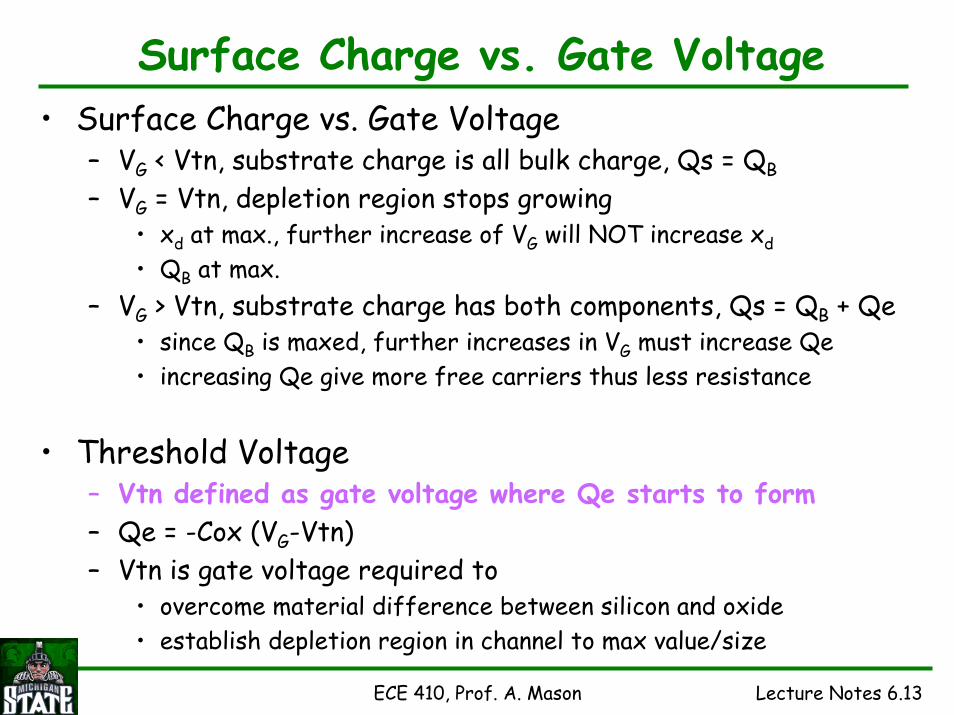
Surface Charge vs. Gate Voltage• Surface Charge vs. Gate Voltage
– VG < Vtn, substrate charge is all bulk charge, Qs = QB
– VG = Vtn, depletion region stops growing• xd at max., further increase of VG will NOT increase xd• QB at max.
– VG > Vtn, substrate charge has both components, Qs = QB + Qe• since QB is maxed, further increases in VG must increase Qe• increasing Qe give more free carriers thus less resistance
• Threshold Voltage– Vtn defined as gate voltage where Qe starts to form– Qe = -Cox (VG-Vtn)– Vtn is gate voltage required to
• overcome material difference between silicon and oxide• establish depletion region in channel to max value/size
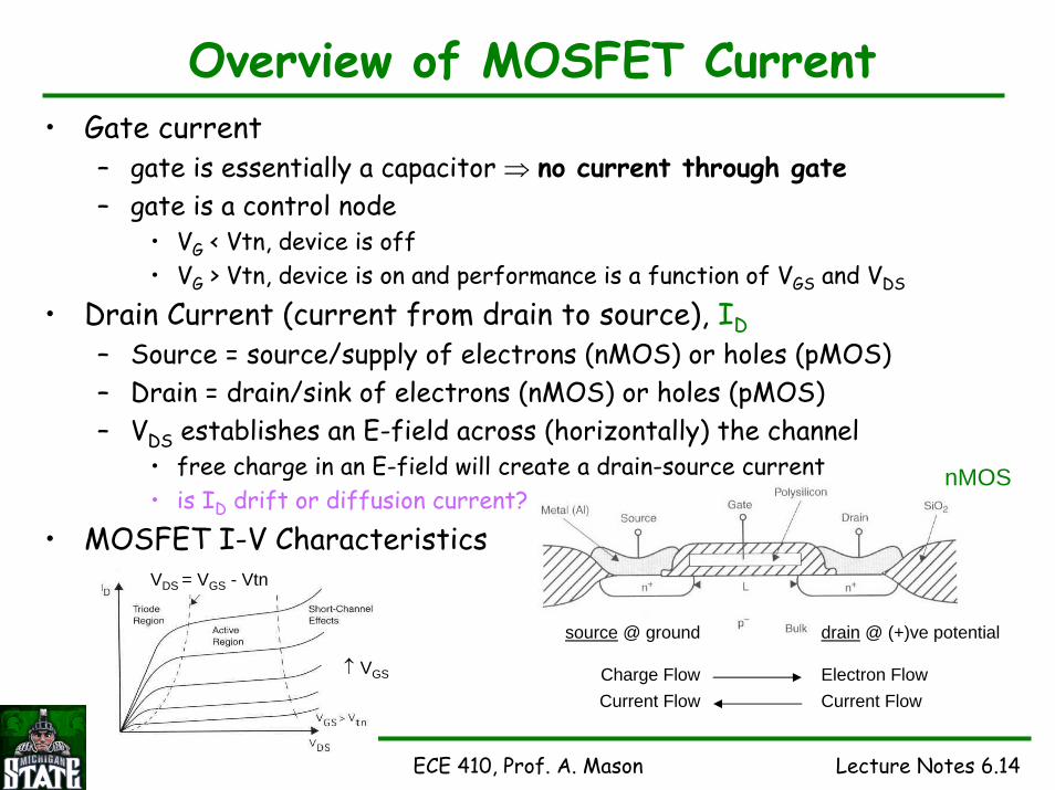
ECE 410, Prof. A. Mason Lecture Notes 6.14
Overview of MOSFET Current• Gate current
– gate is essentially a capacitor ⇒ no current through gate– gate is a control node
• VG < Vtn, device is off• VG > Vtn, device is on and performance is a function of VGS and VDS
• Drain Current (current from drain to source), ID– Source = source/supply of electrons (nMOS) or holes (pMOS)– Drain = drain/sink of electrons (nMOS) or holes (pMOS)– VDS establishes an E-field across (horizontally) the channel
• free charge in an E-field will create a drain-source current• is ID drift or diffusion current?
• MOSFET I-V Characteristics
nMOS
drain @ (+)ve potential
Electron FlowCurrent Flow
source @ ground
Charge FlowCurrent Flow
↑ VGS
VDS = VGS - Vtn

ECE 410, Prof. A. Mason Lecture Notes 6.15
Channel Charge and Current• Threshold Voltage = Vtn, Vtp
– amount of voltage required on the gate to turn tx on– gate voltage > Vtn/p will induce charge in the channel
• nMOS Channel Charge– Qc = -CG(VG-Vtn), from Q=CV, (-) because channel holds electrons
• nMOS Channel Current (linear model:)– I = |Qc| / tt , where tt = transit time, average time to cross channel
• tt = channel length / (average velocity) = L / v• average drift velocity in channel due to electric field E v = μn E• assuming constant field in channel due to VDS E = VDS / L
•
– I = μnCox (W/L) (VG-Vtn) VDS : linear model, assumes constant charge in channel
similar analysis applies for pMOS, see textbook
LL
V
QcIDS
nμ= )(|| VtnVCoxWLQcCoxWLC GG −=⇒=
assumes channel charge isconstant from source to drain

ECE 410, Prof. A. Mason Lecture Notes 6.16
Transconductance and Channel Resistance• nMOS Channel Charge: Qc = -CG(VG-Vtn)• nMOS linear model Channel Current:
– I = μnCox(W/L)(VG-Vtn) VDS• assumes constant charge in channel, valid only for very small VDS
• nMOS Process Transconductance– k’n = μnCox [A/V2] ⇒ I = k’n (W/L) (VG-Vtn) VDS
• nMOS Device Transconductance– βn = μnCox (W/L) [A/V2] ⇒ I = βn (VG-Vtn) VDS– constant for set transistor size and process
• nMOS Channel Resistance– channel current between Drain and Source– channel resistance = VDS / IDS– Rn = 1/( βn (VG-Vtn) )
• pMOS: k’p = μpCox, βp = μpCox (W/L)
similar analysis applies for pMOS,
see textbook
)(
1
tnGSoxn
n
VVLWC
R−
=μ
( )tpSGoxp
p
VVLWC
R−
=μ
1

ECE 410, Prof. A. Mason Lecture Notes 6.17
nMOS Current vs.Voltage• Cutoff Region
– VGS < Vtn⇒ ID = 0
• Linear Region– VGS > Vth, VDS > 0 but very small
• Qe = -Cox (VGS-Vtn)• ID = μn Qe (W/L) VDS
⇒ ID = μnCox (W/L) (VGS-Vtn) VDS
• Triode Region– VGS > Vth, 0 < VDS < VGS-Vth
• surface potential, φs , at drain now f(VGS-VDS=VGD) ⇒ less charge near drain • assume channel charge varies linearly from drain to source
– at source: Qe = -Cox (VGS-Vtn), at drain: Qe = 0⇒
∫=DV
ID yVyQI0
)()( δα
[ ]2)(22 DSDStGS
OXnD VVVV
LWC
I −−=μ
General Integral for expressing ID• channel charge = f(y)• channel voltage = f(y)• y is direction from drain to source
↑ VGS
VDS = VGS - Vtn

ECE 410, Prof. A. Mason Lecture Notes 6.18
nMOS Current vs.Voltage• Saturation Region (Active Region)
– VGS > Vtn, VDS > VGS-Vtn• surface potential at drain, φsd = VGS-Vtn-VDS• when VDS = VGS-Vtn, φsd = 0 ⇒ channel not inverted at the drain
– channel is said to be pinched off• during pinch off, further increase in VDS will not increase ID
– define saturation voltage, Vsat, when VDS = VGS-Vtn• current is saturated, no longer increases• substitute Vsat=VGS-Vtn for VDS into triode equation
⇒2)(
2 tGSOXn
D VVLWC
I −=μ
square lawequation
[ ]2)(22 DSDStGS
OXnD VVVV
LWC
I −−=μ

ECE 410, Prof. A. Mason Lecture Notes 6.19
Other Stuff• Transconductance
– process transconductance, k’ = μn Cox• constant for a given fabrication process
– device transconductance, βn= k’ W/L• Surface Mobility
– mobility at the surface is lower than mobility deep inside silicon– for current, ID, calculation, typical μn = 500-580 cm2/V-sec
• Effective Channel Length– effective channel length reduced by
• lateral diffusion under the gate• depletion spreading from drain-substrate junction
dD XLdrawnLLeff −−= 2)(( )( )
⎟⎟⎠
⎞⎜⎜⎝
⎛ −−=
A
tGDsd qN
VVVX
ε2
GS
L (drawn)
Leff
LDx
d~x
d
D

ECE 410, Prof. A. Mason Lecture Notes 6.20
Second Order Effects• Channel Length Modulation
– Square Law Equation predicts ID is constant with VDS– However, ID actually increases slightly with VDS
• due to effective channel getting shorter as VDS increases• effect called channel length modulation
– Channel Length Modulation factor, λ• models change in channel length with VDS
– Corrected ID equation
• Veff = VGS - Vtn• Body Effect
– so far we have assumed that substrate and source are grounded– if source not at ground, source-to-bulk voltage exists, VSB > 0– VSB > 0 will increase the threshold voltage, Vtn = f(VSB)– called Body Effect, or Body-Bias Effect
( ))(1)(2
2effDStGS
OXnD VVVV
LWCI −+−= λμ

ECE 410, Prof. A. Mason Lecture Notes 6.21
pMOS Equations• Analysis of nMOS applies to pMOS with
following modifications– physical
• change all n-tpye regions to p-type• change all p-type regions to n-type
– substrate is n-type (nWell)• channel charge is positive (holes) and (+)ve charged ions
– equations• change VGS to VSG (VSG typically = VDD - VG)• change VDS to VSD (VSD typically = VDD - VD)• change Vtn to |Vtp|
– pMOS threshold is negative, nearly same magnitude as nMOS– other factors
• lower surface mobility, typical value, μp = 220 cm2/V-sec• body effect, change VSB to VBS

ECE 410, Prof. A. Mason Lecture Notes 6.22
Transistor Sizing• Channel Resistance
“ON” resistance of transistors– Rn = 1/(μnCox (W/L) (VGS-Vtn) )
– Rp = 1/(μpCox (W/L) (VSG-|Vtp|) )
• Cox = εox/tox [F/cm2], process constant
• Channel Resistance Analysis– R ∝ 1/W (increasing W decreases R & increases Current)– R varies with Gate Voltage, see plot above– If Wn = Wp, then Rn < Rp
• since μn > μp• assuming Vtn ~ |Vtp|
– to match resistance, Rn = Rp• adjust Wn/Wp to balance for μn > μp
VGVDD-|Vtp|Vtn
RnRp

ECE 410, Prof. A. Mason Lecture Notes 6.23
Transistor Sizing• Channel Resistances
– Rn = 1/(μnCox (W/L) (VG-Vtn) )– Rp = 1/(μpCox (W/L) (VG-|Vtp|) )– Rn/Rp = μn/μp
• if Vtn = |Vtp|, (W/L)n = (W/L)p
• Matching Channel Resistance– there are performance advantage to setting Rn = Rp
• discussed in Chapter 7– to set Rn = Rp
• define mobility ratio, r = μn/μp• (W/L)p = r (W/L)n
– pMOS must be larger than nMOS for same resistance/current
• Negative Impact– ⇒ CGp = r CGn larger gate = higher capacitance
How does this impactcircuit performance?

ECE 410, Prof. A. Mason Lecture Notes 6.24
MOSFET RC Model• Modeling MOSFET resistance and capacitance is very
important for transient characteristics of the device• RC Model
• Drain-Source (channel) Resistance, Rn– Rn = VDS / ID
• function of bias voltages– point (a), linear region
• Rn = 1/[βn(VGS-Vtn)]– point (b), triode region
• Rn = 2/{βn[2(VGS-Vtn)-VDS]}– point (c), saturation region
• Rn = 2VDS / [βn (VGS-Vtn)2]– general model equation
• Rn = 1/[βn(VDD-Vtn)]
time constant at drain, τDτD = CD Rn

ECE 410, Prof. A. Mason Lecture Notes 6.25
MOSFET Capacitances -Preview• Need to find CS and CD
• MOSFET Small Signal model– Model Capacitances
• Cgs• Cgd• Cgb• Cdb• Csb• no Csd!
• MOSFET PhysicalCapacitances– layer overlap– pn junction
+v-
gs
vsis
vg vd
idg vmb sbg vm gs
roCgs
Cgb
Csb
Cdb
CgdGate Drain
Source
Body (Bulk)

ECE 410, Prof. A. Mason Lecture Notes 6.26
RC Model Capacitances• Why do we care?
– capacitances determine switching speed• Important Notes
– models developed for saturation (active) region– models presented are simplified (not detailed)
• RC Model Capacitances– Source Capacitance
• models capacitance at the Source node• CS = CGS + CSB
– Drain Capacitance• models capacitance at the Drain node• CD = CGD + CDB What are CGS, CGD, CSB, and CDB?

ECE 410, Prof. A. Mason Lecture Notes 6.27
MOSFET Parasitic Capacitances• Gate Capacitance
– models capacitance due to overlap of Gate and Channel• CG = Cox W L
– estimate that CG is split 50/50 between Source and Drain• CGS = ½ CG
• CGD = ½ CG
– assume Gate-Bulk capacitance is negligible• models overlap of gate with substrate outside the active tx area• CGB = 0
• Bulk Capacitance– CSB (Source-Bulk) and CDB (Drain-Bulk)
• pn junction capacitances
⎟⎟⎠
⎞⎜⎜⎝
⎛
Ψ+=
0
1 Rjoj
VCC ( )2
1
02 ⎥⎦
⎤⎢⎣
⎡+Ψ
=DA
DAjo NN
NNqAC ε
What are VR, Ψ0, NA, and ND?
NA
ND

ECE 410, Prof. A. Mason Lecture Notes 6.28
MOSFET Junction Capacitances• Capacitance/area for pn Junction
• S/D Junction Capacitance– zero-bias capacitance
• highest value when VR = 0, assume this for worst-case estimate• Cj = Cjo
– CS/Dj = Cjo AS/D, AS/D = area of Source/Drain
• what is AS/D?• complex 3-dimensional geometry
– bottom region and sidewall regions
– CS/Dj = Cbot + Csw• bottom and side wall capacitances
21
02 ⎥⎦
⎤⎢⎣
⎡Ψ
= Ajo
NqC ε
assuming ND (n+ S/D) >> NA (p subst.)
jm
Rjoj
VCC ⎟⎟⎠
⎞⎜⎜⎝
⎛Ψ
+=0
1
mj = grading coefficient (typically 1/3)
⎟⎟⎠
⎞⎜⎜⎝
⎛=Ψ 20 ln
i
DAT n
NNV

ECE 410, Prof. A. Mason Lecture Notes 6.29
Junction Capacitance• Bottom Capacitance
– Cbot = Cj Abot• Abot = X W
• Sidewall Capacitance– Csw = Cjsw Psw
• Cjsw = Cj xj [F/cm]– xj = junction depth
• Psw = sidewall perimeter – Psw = 2 (W + X)
• Accounting Gate Undercut– junction actually under gate also due to lateral diffusion– X ⇒ X + LD (replace X with X + LD)
• Total Junction Cap– CS/Dj = Cbot + Csw = Cj Abot + Cjsw Psw = CS/Dj
xj

ECE 410, Prof. A. Mason Lecture Notes 6.30
MOSFET Bulk Capacitances• General Junction Capacitance
– CS/Dj = Cbot + Csw• CSB (Source-Bulk)
– CSB = Cj ASbot + Cjsw PSsw• CDB (Drain-Bulk)
– CDB = Cj ADbot + Cjsw PDsw
• RC Model Capacitances– Source Capacitance
• CS = CGS + CSB– Drain Capacitance
• CD = CGD + CDB
+v-
gs
vsis
vg vd
idg vmb sbg vm gs
roCgs
Cgb
Csb
Cdb
CgdGate Drain
Source
Body (Bulk)

ECE 410, Prof. A. Mason Lecture Notes 6.31
Junction Areas• Note: calculations assume following design rules
– poly size, L = 2λ– poly space to contact, 2λ– contact size, 2λ– active overlap of contact, 1λ
• Non-shared Junction with Contact– Area: X1 W = (5)(4) = 20λ2
– Perimeter: 2(X1 + W) = 18λ• Shared Junction without Contact
– Area: X2 W = (2)(4)λ2 = 8λ2
– Perimeter: 2(X2 + W) = 12λ• much smaller!
• Shared Junction with Contact– Area: X3 W = (6)(4)λ2 = 24λ2
– Perimeter: 2(X3 + W) = 20λ• largest area!
W = 4λX1 = 5λ, X2= 2λ, X3 = 6λ⇒
X1
X2
X3


![Microscopic strength of silicon particles in an aluminium ... · mine the alloy's deformation and fracture properties [3,5e7,15,21,24,25,29e36]. Yet, little is known of the intrinsic](https://img.pdfslide.us/doc/110x75/5e7bf66c2469b864f574c07c/microscopic-strength-of-silicon-particles-in-an-aluminium-mine-the-alloys-deformation.jpg)