Embed Size (px)
Citation preview

Photoluminescence Properties of Silicon Nanocrystallites
by
Arun A. Seraphin
B.A. Political ScienceB.E. Engineering Science
State University of New York at Stony Brook, 1991
Submitted to the Department of Materials Science and Engineeringin partial fulfillment of the requirements for the degree of
Doctor of Philosophy in Electronic Materials
at theMassachusetts Institute of Technology
June 1996
@ 1996 Massachusetts Institute of Technology. All rights reserved.
Signature of Author:Departmentrof Matenais 3cience and Engineering
May 3, 1996
Certified by:Kirk D. Kolenbrander
Associate Professor of Electronic MaterialsThesis Supervisor
Accepted by:Michael F. Rubner
TDK Professor of Materials Science and EngineeringChair, Departmental Committee on Graduate Students
OF TECHNOLOGY
JUN 241996 nc
LIBRARIES


Photoluminescence Properties of Silicon Nanocrystallites
by
Arun A. Seraphin
Submitted to the Department of Materials Science and Engineeringon May 3, 1996 in Partial Fulfillment of the Requirements
for the Degree of Doctor of Philosophy in Electronic Materials
ABSTRACT
A great deal of attention focuses on the visible light emitting properties of siliconnanostructures because of their potential use in optoelectronic applications. The origin ofthe emitted light and the role that the particle sizes and surfaces play in the emissionmechanism are still under considerable debate. To study these questions, thin films of Sinanocrystallites have been deposited using a novel pulsed laser ablation supersonicexpansion source. The films consist of a polydisperse collection of crystalline Si particlesembedded in a native oxide matrix which efficiently emits visible light under ultravioletphotoexcitation. The films have been treated using a number of post-depositionprocessing steps, including hydrofluoric acid and nitric acid etches and oxidation furnacetreatments, in order to control the sizes and surfaces of the Si particles. The films havebeen characterized using photoluminescence emission spectroscopy and x-rayphotoelectron spectroscopy to correlate the sizes and surface properties to theluminescence behavior. Additionally, the non-linear optical response of the films has beenstudied using degenerate four-wave mixing spectroscopy.
Particle size determines the emission energy of the films through the quantumconfinement of photoexcited carriers. Nanostructure size has been controlled through theuse of acid etch/oxide regrowth cycles. This has resulted in a consistent blueshift of theemission energy, as is predicted by theories of quantum confinement in semiconductornanostructures. Both the photoluminescence temperature and pump power dependenceare consistent with emission due to a recombination of quantum confined carriers.
Optical properties are also strongly influenced by the extent of surface passivation,which controls the density of nonradiative recombination centers. Neither unpassivated,gas phase nanoparticles nor as-deposited unpassivated thin films show visibleluminescence behavior, while films processed to passivate their surfaces show efficientvisible emission. Surface passivation also improves the nonlinear optical response of thefilms. Hydrogen, oxygen, and iodine have been used to passivate the nanostructuresurfaces. While the emission intensity scales with the extent of surface passivation, theemission energy is independent of the specific chemical nature of the passivating speciesand is only determined by particle size.
Thesis Supervisor: Kirk D. KolenbranderTitle: Associate Professor of Electronic Materials

I I

Table of Contents
List of Figures 9Acknowledgments 14
1. Introduction 171.1 Thesis Outline 171.2 Motivation: Si Photonics and Optoelectronics 171.3 Materials Choices I: Silicon 221.4 Materials Choices II: Light Emitting Silicon 25
1.4.1 Impurities 251.4.2 Si Based Alloys 261.4.3 Amorphous Silicon 271.4.4 Polysilanes and Polymers 281.4.5 Quantum Confined Silicon Structures 28
1.5 Quantum Confinement Effects in Semiconductors 281.6 Semiconductor Nanostructures 35
1.6.1 Cadmium Selenide 351.6.2 Germanium 371.6.3 Other Materials Systems 37
1.7 Silicon Nanostructures 381.7.1 Silicon Nanostructure Synthesis 38
1.7.1.1 Porous Silicon Formation 381.7.1.2 Nanocrystalline Silicon Formation 42
1.7.2 Light Emission From Silicon Nanostructures 431.7.2.1 Amorphous Silicon 431.7.2.2 Siloxene and Related Materials 461.7.2.3 Oxide Defects 471.7.2.4 Surface States 501.7.2.5 Quantum Confinement 52
1.7.3 Structure and Size 551.7.4 Light Emitting Devices 57
1.8 Recombination Mechanism 581.8.1 Radiative Recombination 58
1.8.1.1 Excitonic Recombination 601.8.1.2 Band to Band Transitions 621.8.1.3 Impurity Level Transitions 621.8.1.4 Intraband Transitions 63
1.8.2 Nonradiative Recombination 631.8.2.1 Phonon Emission 641.8.2.2 Auger Recombination 641.8.2.3 Surface and Defect Recombination 65
1.9 Silicon Processing Basics 671.9.1 Oxidation of Silicon 67

1.9.2 Etching of Silicon and Oxides 701.9.2.1 Stain Etched Porous Silicon 71
1.10 Surfaces 731.10.1 Nanocrystalline Silicon Surfaces 731.10.2 Surface Structure 741.10.3 Electronic Structure 75
1.10.3.1 Dangling Bonds 761.10.3.2 Surface Defect States 761.10.3.3 Adsorbed Materials 77
1.11 Objectives and Outline 781.11.1 Questions 78
1.11.1.1 Can optically active silicon nanostructures besynthesized by pulsed laser ablation supersonicexpansion? 78
1.11.1.2 What role does nanostructure size play incontrolling optical behavior? 79
1.11.1.3 What role does nanostructure surface play indefining optical behavior? 79
1.11.2 Proposed Work 80Chapter 1 References 81
2. Experimental Procedure 862.1 Nanocrystallite Film Synthesis 86
2.1.1 Pulsed Laser Ablation Supersonic Expansion System 862.1.1.1 Deposition Rate 92
2.2 Materials 922.2.1 Target Rods 922.2.2 Substrates 92
2.3 Processing 932.3.1 Aging 942.3.2 Wet Chemical Treatments 94
2.3.2.1 Hydrofluoric Acid Dip 942.3.2.2 Nitric Acid Dip 942.3.2.3 Boiling Water Treatment 952.3.2.4 HF/HNO3/H 20 Treatments 952.3.2.5 Methanol and Iodine:Methanol Dips 95
2.3.3 Oxidation Furnace Treatments 952.4 Photoluminescence Emission Spectroscopy 96
2.4.1 Basics 962.4.2 Experimental Setup 96
2.4.2.1 Lasers and Optics 962.4.2.2 Detector 982.4.2.3 Data Collection and Processing 982.4.2.4 Absolute Intensities and Wavelengths 992.4.2.5 Temperature Control of Films 100

2.4.2.6 Gas Phase Photoluminescence 1002.5 Degenerate Four Wave Mixing 101
2.5.1 Experimental Setup 1012.6 Other Characterization Techniques 103
2.6.1 X-ray Photoelectron Spectroscopy 1032.6.1.1 XPS Basics 1032.6.1.2 Experimental Details 103
2.6.2 Fourier Transform Infrared Spectroscopy 1052.7 Films 105
2.7.1 Structure 1052.7.1.1 Nanocrystallite structure 107
2.7.2 Properties 1092.7.3 Comparison with Porous Silicon 110
Chapter Two References 111
3. Results and Discussion 1123.1 Photoluminescence 112
3.1.1 Size Distribution of Nanocrystallites 1143.2 Processing Effects on Luminescence 118
3.2.1 Size Effects 1183.2.1.1 Aged Films 1183.2.1.2 HF/HNO3 Cycles 1213.2.1.3 HF/HNO 3/H20 Dip Times 1233.2.1.4 Deposition Parameter Control of Size 1233.2.1.5 Oxidation Furnace Treatments 1233.2.1.6 Summary 125
3.2.2 Surface Effects 1273.2.2.1 Gas Phase Photoluminescence 1273.2.2.2 Atmospheric Aging: Oxide Passivation 1293.2.2.3 Chemical Treatments 1293.2.2.4 Effect of Dip Time on Luminescence Intensity 1333.2.2.5 Methanol Quenching of Luminescence 1353.2.2.6 Halogen Passivation 1383.2.2.7 Summary 141
3.3 Temperature Dependence of Photoluminescence Emission 1413.3.1 Temperature Dependence in Light Emitting Silicon 1423.3.2 Temperature Dependence in Silicon Nanocrystallites 144
3.4 Surface Characterization of Silicon Nanocrystallites 1513.4.1 Passivating Species by Infrared Spectroscopy 1513.4.2 Surface Species by X-ray Photoelectron Spectroscopy 154
3.4.2.1 Hydride and Oxide Passivation of Silicon 1543.4.2.2 Effect of Methanol Dip 1583.4.2.3 Halogen Passivation 158
3.5 Nonlinear Optical Response 1653.6 Excitation Intensity 171
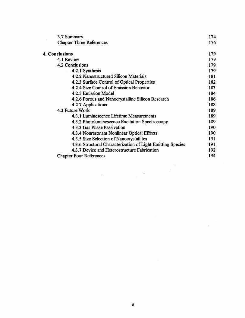
3.7 Summary 174Chapter Three References 176
4. Conclusions 1794.1 Review 1794.2 Conclusions 179
4.2.1 Synthesis 1794.2.2 Nanostructured Silicon Materials 1814.2.3 Surface Control of Optical Properties 1824.2.4 Size Control of Emission Behavior 1834.2.5 Emission Model 1844.2.6 Porous and Nanocrystalline Silicon Research 1864.2.7 Applications 188
4.3 Future Work 1894.3.1 Luminescence Lifetime Measurements 1894.3.2 Photoluminescence Excitation Spectroscopy 1894.3.3 Gas Phase Passivation 1904.3.4 Nonresonant Nonlinear Optical Effects 1904.3.5 Size Selection of Nanocrystallites 1914.3.6 Structural Characterization of Light Emitting Species 1914.3.7 Device and Heterostructure Fabrication 192
Chapter Four References 194

List of Figures
Figure 1-1 Schematic of an optoelectronic 8 x 8 crossbar switch. 19
Figure 1-2 Schematic of proposed photonic switch using semiconductor 20nanocrystallites as active switch material.
Figure 1-3 Schematic comparison of direct and indirect semiconductor band 24structures.
Figure 1-4 Density of states as a function of increasing dimensional confinement. 30
Figure 1-5 Schematic of saturable absorption behavior in the nonlinear optical 32switch based on semiconductor nanocrystallites. The pump beam is used tosaturate the absorption of the nanocrystallites to make it transparent to the signalbeam.
Figure 1-6 Theoretical calculation of energies of band edges and band gap in 34nanocrystalline silicon. 0 K band gap of bulk silicon is shown for comparison.
Figure 1-7 Shift in room temperature optical absorption with changing size in 36CdSe nanocrystallites dispersed in hexane.
Figure 1-8 Apparatus used for the anodic etching of silicon wafers to form porous 39silicon.
Figure 1-9 Schematic of proposed structure of porous silicon. Porous silicon 41contains nanoscale wire and nanocrystallite regions, as well as amorphous siliconand oxide.
Figure 1-10 Key properties of observed emission bands from porous silicon. 44These are the characteristics typically reported in the literature.
Figure 1-11 Typical red band photoluminescence spectrum from porous silicon. 45
Figure 1-12 Kanemitsu model of density of states in oxidized silicon 48nanocrystallites. There are two luminescent centers, the core and surface states.The density of states falls of exponentially from the level of the core states. Higherenergy transitions represent core state recombination, while lower energytransitions are coupled to localized surface states.
Figure 1-13 Model of non-bridging oxygen hole centers (NBOHCs) at disordered 49porous silicon-oxide interface. Center consists of a trapped hole on a Si-O'complex in the interfacial region.

Figure 1-14 Koch surface state model of porous silicon luminescence. Eo 51transitions represent excitonic recombination in core of crystallite. E1 transitionsrepresent recombination coupled to one localized surface state. E2 emissions arelow energy transitions are between two localized surface states. Surface defects actas nonradiative recombination centers.
Figure 1-15 Correlation of PL peak energy from porous silicon with Si-O/Si-H 53bond ratio as measured by FTIR.
Figure 1-16 Correlation between emission energy and size as measured by PL, 54TEM, NEXAFS, and EXAFS for oxidized silicon nanocrystallites produced bydisilane pyrolysis and porous silicon. Also shown are theoretical calculations forsize as a function of silicon coordination in nanostructures.
Figure 1-17 Schematic of radiative recombination mechanisms in semiconductors. 59Pictured are: Excitonic recombination in direct (A) and indirect (B) gap materials;band-to-band recombination in direct (C) and indirect (D) materials; shallowtransition to donor (E) and acceptor (F) states; deep transitions to acceptor (G)and from donor (H) states; and donor-acceptor (I) transition.
Figure 1-18 Low temperature luminescence from n-type bulk silicon showing 61excitonic luminescence and a number of phonon related peaks.
Figure 1-19 Model for effect of defect state on energy band and density of states 66of semiconductor. Defects create a continuum of states in gap which act as anonradiative pathway for the relaxation of excited carriers. L represents the carrierdiffusion length and r the defect radius.
Figure 1-20 Proposed mechanism for etching of silicon by hydrofluoric acid. 72Silicon is removed in H2SiF6 complexes, leaving the surface hydrogen terminated.
Figure 2-1 Schematic of stainless steel block used in pulsed laser ablation 87supersonic expansion system.
Figure 2-2 Top view schematic of pulsed laser ablation supersonic expansion 89system.
Figure 2-3 Schematic of photoluminescence experimental setup. 97
Figure 2-4 Schematic of degenerate four wave mixing spectroscopy (DFWM) 102experimental setup.

Figure 2-5 Schematic of thin film of silicon nanocrystallites embedded in native 106oxide matrix on substrate material. Deposition is drawn to highlight sizedistribution present in all films.
Figure 2-6 High resolution electron micrograph of a silicon nanocrystallite 108deposited on an amorphous carbon substrate.
Figure 2-7 High resolution electron micrograph of a silicon nanocrystallite with an 108amorphous surface layer.
Figure 3-1 Typical photoluminescence spectrum for a thin film of silicon 113nanocrystallites on a Teflon substrate. Spectrum was taken at 300 K using a3xNd:YAG (,ex= 355 nm) laser as the excitation source.
Figure 3-2 Size distribution calculated from PL spectrum in Figure 3-1 using 115Khurgin model.
Figure 3-3 PL spectrum from a defect ridden oxide (glass slide) at 300 K showing 117significant sub-550 nm spectral structure.
Figure 3-4 Effect of aging in atmosphere on PL spectrum of silicon nanocrystallite 119thin films. PL wavelength blueshifts with increased aging, consistent withcrystallite size reduction due to extended oxidation.
Figure 3-5 Effect of HF/HNO3 cycles on PL emission. As etch/oxide regrowth 122cycles reduce the size of the silicon nanocrystallites, a blueshift in the emission isobserved.
Figure 3-6 Effect of increasing dip time in HF/HNO3/H20 solution. As dip time 124increases and silicon nanocrystallite size is reduced, a blueshift in emission isobserved.
Figure 3-7 Comparison of PL spectra for aged and oxidation furnace treated 126samples. The furnace treated sample has lost its red band behavior and shows theblue signal indicative of oxide emission.
Figure 3-8 Comparison of PL spectra of atmospherically aged, vacuum aged, and 130as deposited films. Only the surface passivated, air-aged sample shows anyemission intensity.
Figure 3-9 Comparison of samples treated in HF, HNO3, and boiling water. All 131three show luminescence behavior indicating passivation of the nanocrystallitesurfaces.

Figure 3-10 Effect of increasing HF dip time on PL spectra of silicon 134nanocrystallite thin films. With increasing dip time and enhanced surfacepassivation, emission efficiency improves.
Figure 3-11 PL spectra of HF dipped film before and after methanol treatment. 136Methanol significantly reduces the luminescence intensity of the H-passivatedsample.
Figure 3-12 PL spectra of an aged (oxide passivated) sample before and after a 137methanol dip.
Figure 3-13 Comparison of the PL spectra of an aged (oxide passivated) film 139before and after 12 treatment.
Figure 3-14 PL spectra of an aged (oxide passivated) sample and an HF dipped 140(H-passivated) sample treated with 12.
Figure 3-15 Energy gap of bulk silicon as a function of temperature. 143
Figure 3-16 Shift in peak PL energy of thin film of silicon nanocrystallites as 145temperature is reduced from 300 K.
Figure 3-17 Full width at half maximum (FWHM) of the PL spectrum of a thin 148film of silicon nanocrystallites as a function of temperature.
Figure 3-18 Relative shift in blue and red edge of PL emission spectrum of a thin 149film of silicon nanocrystallites as temperature is reduced from 300 K. The blueedge shows a larger shift to higher energies as temperature is reduced.
Figure 3-19 Temperature dependence of the intensity of PL emission at 640 nm 150for a thin film of silicon nanocrystallites.
Figure 3-20 FTIR spectra of a silicon nanocrystallite thin film showing the 152reduction in the -1100 cm'n oxide stretch mode after a dip in hydrofluoric acid.
Figure 3-21 Comparison of the FTIR spectra of HF dipped and undipped silicon 153nanocrystallite thin films. There is an increase in the Si-H 2 scissor mode at -900cm"1 after the HF treatment.
Figure 3-22 Comparison of Si 2p XPS spectra for HF treated and aged silicon 155nanocrystallite thin films. Aged film shows development of Si4+ behavior at -103eV.
Figure 3-23 The chemical shift in binding energy of the Si 2p XPS line for 157elemental Si and SiOz.

Figure 3-24 Comparison of Si 2p XPS spectra for an aged (O-passivated) thin film 159of silicon nanocrystallites before and after a methanol dip. There is no change inthe ratio of oxidized to unoxidized silicon as a result of the treatment.
Figure 3-25 Effect of methanol treatment on Si 2p XPS signal of an H-passivated 160thin film of silicon nanocrystallites.
Figure 3-26 Effect of iodine treatment on Si 2p XPS spectrum of O-passivated 161silicon nanocrystallite thin film.
Figure 3-27 Si 2p XPS spectra of aged, HF dipped, and 12 treated silicon 163nanocrystallite thin films. The change in ratio of oxidized to unoxidized silicon inthe 12 sample, as compared to the HF treated sample, indicates that I is bonding tothe surface and changing its oxidation state.
Figure 3-28 I 3ds,2 XPS spectrum of H-passivated silicon nanocrystallite thin film 164treated with iodine.
Figure 3-29 Third order nonlinear optical susceptibility X(3) at 532 nm for 167passivated nanocrystallites, unpassivated nanocrystallites, and bulk polycrystallinesilicon as measured by degenerate four wave mixing spectroscopy (DFWM).
Figure 3-30 Absorption spectrum of HF treated thin film of silicon nanocrystallites 168on poly(vinyl carbonate) substrate.
172Figure 3-31 PL intensity dependence on excitation intensity. Differentwavelengths are plotted to highlight difference in red-orange emission behavior andblue emission behavior.
Figure 3-32 PL spectra from a thin film of silicon nanocrystallites at increasing 173excitation intensities. A pulsed 3xNd:YAG laser was used as the excitation source.As excitation intensity increases, PL emission intensity increases and shifts to higherenergies.

Acknowledgments
I have decided that this should be a list of things to remember about graduate school,
in case I someday want to look back to my time at MIT. I'm pretty sure I don't like MIT as
an institution, or the attitudes it seems to encourage, or the way it treats its people. I'm sure
the reason I was able to stay and even enjoy my time there had everything to do with the
people I got to meet and work with, and almost nothing to do with the "great science" or
"excellence" for which MIT is famous. I am grateful for these people, and I guess I thank
MIT for bringing them together in such a unique environment.
First, I would like to thank my thesis advisor, Professor Kirk Kolenbrander. I was told
more than once that there was only one professor I could have possibly worked for here, and I
was lucky enough to find him. Professor Kolenbrander has taught me a lot, not just about
science and research, but also about being a good person and father and teacher. We have
often disagreed about my choices throughout this process, but I always felt grateful that he
supported me whenever I really needed it. I consider him a mentor, role model, and friend,
and will never forget his patience despite all the things I have put him through.
I did some science while at MIT, and it was fun and challenging, and I learned more
than I could have ever imagined. I express my sincere gratitude to the people who helped me
accomplish what's in this thesis. Special thanks go to my thesis committee: Professors
Thompson, Chiang, and Kimerling for their insights and feedback on the work. The technical
assistance of Francisco Aranda, Das Chowdhury, and Jurgen Michel is very much appreciated.
By far the people who taught me the most were the various members of the
Kolenbrander research group. I will always be grateful for the chance to work with and
befriend my fellow students: Leon Chiu, Tracey Burr, Eric Werwa, Shih-Tung Ngiam, Shuba
Balasubramanian, and Danielle Russell. This was and is a great bunch of people, who always
seemed to give me more then I ever gave back in return. It was always very light and a lot of
fun to be in the lab, and we sometimes even managed to get some good science done on the
side. Of everything about grad school, I will miss the group most of all. For the record, here
is an honor roll of all the other folks who served time in 13-5044: Bobby Korn, Stacy
Holander, Teresa Lau, Jen Brady, Cade Murray, Jen McMurray, Devin MacKenzie, Jeanette

Ryan, Chuxin Zhou, Bob Martinez, Yoli Leung, Julie Ngau, Andrea Santoro, Anna Lena
Thilderkvist, and Jimmie Walker. I can't fail to mention Morgan Kennedy, Ed Mellinger, and
Peter Heron (whose antics were the stuff of legend), for their periodic counseling sessions and
understanding.
Without a doubt, my time at MIT would have been unbearable without an assortment
of people and events that kept me functioning, like baby-sitting and dinners in Natick; going to
Fenway with Naveen; lunch at 11:30 and coffee at 3 with Doug, Erika, Erin, and Hal; and
John Matz trying to help me get big. I am thankful for roommates (Hiten, Jen, Patrick,
Mohammed, and Amir); TV folks (Tara Macpherson, CCTV, and Rob at the Center); stir-
fried chicken and a soda at the trucks; weddings; Nat's CD player and Allison Engine; the
Walt Disney CompanyTM; poker at Peter's; 13-4009B; Mike Dauenheimer and the art of
conventions; the secret garden; the Draper crowd at the Muddy; sneaking out to see movies;
and my buddies at Fresco's. And of course Howard, Robin, Jackie, Fred, and Gary.
I will always remember the great people who were a part of my life during this time.
Thanks for everything to: Heather, Annie, Mike, Kate, Brett, Cherie, Ann and Locksee,
Laura, Jim, Jay, Ali, Jeff, Kumiko, Rita, as well as to all the other cool people who took time
out of their busy MIT lives to stop and chat in the hall, or get a reference, or join the slack
train. They made MIT and my time in Boston more "human".
I am grateful for the encouragement of my family, especially Vinod and Mary Anne,whose home was a great escape from graduate school. I particularly thank my parents, who
always heard about the worst of MIT through my miserable phone calls home. Their unfailing
support and understanding enabled me get through. Finally, I would like to thank my nieces
and nephews (Ivy, Peter, Audrey, and Stephen), who I bragged about nonstop, and whose
happy faces in pictures on my office wall could always cheer me up, no matter how bad MIT
was being to me. I dedicate this work to you, for all the joy you have brought into my life.
5/21/96

SII

1. Introduction
1.1 Thesis Outline
This thesis is divided into four parts. Chapter 1 provides some motivation for the
study of silicon nanocrystallites, reviews the basic issues and fundamental physics relevant to
the field, and defines the questions that will be addressed in this work. Chapter 2 describes
the experimental techniques used in the synthesis and characterization of the films, as well as a
brief description of the structural properties of the as deposited films used in the optical
experimentation. Chapter 3 focuses on the processing and optical characterization of the films
and descriptions of the physical phenomena that the observed behaviors imply. Chapter 4
summarizes the work by drawing conclusions as to the origins and potential usefulness of the
observed properties, as well as proposing some avenues for future research.
1.2 Motivation: Silicon photonics and optoelectronics
The continual push for higher speed and lower cost telecommunications and
information processing have led to attempts to engineer new devices that can fulfill demanding
technical specifications and exploit new potential market opportunities. In particular, the
fields of optoelectronics, using electronics to manipulate optical signals, and photonics, using
light to control optical signals, may provide the foundation on which these new technologies
can be built. The development of optoelectronic devices, such as lasers, detectors, and light
emitting diodes, and photonic devices, such as directional couplers and all-optical switches,have been spurred by the need to improve the speed and quality of information flow, while
reducing device dimensions and manufacturing costs. Silicon based devices and materials are
a clear step in these directions, for they can fulfill many of the strict materials engineering and
performance requirements presented by the potential opportunities in photonics and
optoelectronics, in a well established commercial technology.

One of the many opportunities in photonic devices revolves around the ability to
switch information flow. The progression of information switching technology from the
mechanical switching of the telegraph to the electronic switching of signals in fiber optic
networks has increased transmission rates roughly 2 billion times. However, new demands for
global voice, video, and data transmission will require further improvements in transmission
rates and switching speed, which can be provided by the development of all-optical switching
technology.
A typical optoelectronic switch in use today is shown in Figure 1-1. This 8x8 crossbar
switch consists of an array of 8 photodetectors linked through an electronic switch circuit to
an array of 8 light emitting diodes (LEDs).' The optoelectronic devices at either end of this
package are coupled to fiber optic cables which transmit information signals in the form of
light. The optical signals are converted to electronic pulses in the detectors and passed to the
switch circuit, where they are logically processed. The electronic signal is then sent to an
appropriate LED and finally reconverted into an optical signal for transmission on the
downstream fiber. This switching system is slowed down by the two required conversions
between photons and electrons as signal carriers, as well as the limitation that a typical
electronic switch can only handle one incoming and outgoing signal at a time.
In contrast, a photonic switch could improve on the speed of this type of system. The
proposed system shown in Figure 1-2 would use a pump beam to gate the flow of a signal
beam by exploiting an optical nonlinearity in a switch placed in the waveguiding material. The
high switching speed of such a system would be based on the extremely fast nonlinearities in
the switch material, in this case semiconductor nanocrystallites, and the removal of the
previously required step of conversions to slower electronic signals. In addition, by tuning the
resonance frequency of this nonlinearity it would be possible to utilize signals on a number of
wavelengths at the same time, assuming efficient transmission through the waveguides.
Finally, this passive system requires no external power supply, and by eliminating electronics,
eliminates problems of electrical noise and crosstalk.
The production of a photonic device such as this switch awaits the development of
nonlinear optical materials which meet the requirements of such a system. The materials
should show strong and fast optical nonlinearities for efficient switching. They should be

Optoelectronic Switch
I % X
OpticalMk
/// ElectronicBank
-Optical
Fibers
tPhotodetector
Array
Figure 1-1 Schematic of an optoelectronic 8 x 8 crossbar switch. (From Ref 1)
LEDArray
!K .A.\cS
=-I I, Q I \ I

Signc
Figure 1-2 Schematic of proposed photonic switch using semiconductor nanocrystallites asactive switch material.

reliable and defect free when produced. Finally, the materials should be easily integrable with
existing growth and processing techniques and device architectures, to ensure successful wide
scale commercialization and profitable deployment of the technology.
Opportunities in optoelectronic devices revolve around similar themes. There is a
constant drive for miniaturization of computer technology, producing exponential growth of
device densities in integrated circuitry, and creating new device fabrication and materials
processing challenges. As the power of microprocessors increases alongside this
miniaturization, the requirements for electrical connections on smaller scales is leading to an
electronic bottleneck on the chip and board level. A rule of thumb for partitions of large
computer systems is Rent's rule which states that the number of input/output connections for
a system of chips containing N logic elements is N .2 For a chip system using 100,000 logic
elements, this requires 2100 pinouts. This large number creates spatial problems that can be
eased by moving from electronic signals to optical signals. A typical optical pinout requires
over 50 times less space than an equivalent electrical bonding pad, providing freedom for
design of device architecture and allowing for further miniaturization.3 However, the
production of these optical circuit elements requires the development of optoelectronic
technology that is compatible with existing microelectronic technology on this scale.
Additionally, a great savings in cost and time can be achieved by moving from systems which
utilize many different materials to integrated systems based on one material. For example, the
optoelectronic switch in Figure 1-1 can have silicon photodetectors and electronics with
present technology, but cannot use silicon LEDs. There would be a great savings in
production time and cost if such a switch could be made using all silicon-based technology.
Again, the production of these new optoelectronic devices requires the development of
new materials first. The materials must as always be easily grown and processed reliably to
device specifications. The development of optoelectronic materials for display applications
demands production of tunable, visible, and efficient light emitters. Emitters for fiber optic
transmission must be compatible with fiber optic technology, for example, taking advantage of
the dispersion minimum at a wavelength of 1.54 microns in silica fibers. The new materials
also need to be compatible with future miniaturization needs, as well as easily integrable into
existing electronics and device manufacturing regimens for commercial success.

1.3 Materials Choices I: Silicon
Given the opportunities and requirements in areas of photonic and optoelectronic
applications, one clear choice of material is silicon. As the basis of the entire microelectronics
industry, silicon is the focus of billions of dollars of investment and decades worth of technical
expertise on the growth and processing of electronics grade materials and the design and
performance of devices. New technologies based on silicon can tap into these advantages to
outstrip competitors.
Silicon is an elemental semiconductor of with an energy band gap of 1.12 eV, and can
be easily doped using a variety of impurities to alter its conductivity over many orders of
magnitude. Control of the impurity type can change the nature of the dominant conduction
processes from conduction by negative charge carriers (electrons) to conduction by positive
charge carriers (holes). Adjusting the doping levels down to concentrations of one part per
million can drastically change the overall conductivity of the material. This control of the
electronic properties of silicon makes it an ideal system for use in device technologies.
The major advantage of silicon over other potential photonic and optoelectronic
materials is in growth and processing knowledge and costs. Crystalline silicon can be
produced today regularly with impurity and defect levels of less than one part in ten billion. It
was the development of this level of defect control in bulk silicon that made possible the
implementation of the device concepts that stemmed from the invention of the transistor by
Shockley, Bardeen, and Bratton in 1947. Silicon processing has developed so that its costs
are much less than its typical semiconductor rivals for both wafers and devices.
Silicon processing technology has developed alongside the growth of the
microelectronics industry. Today, silicon can easily be grown in bulk form from the melt and
in thin films using a variety of vapor phase techniques. Silicon growth can neglect the often
difficult problems of maintaining stoichiometry that are faced during the synthesis of
compound semiconductor materials. Silicon has a native oxide (SiO 2), which can be easily
grown and etched using a variety of techniques that have already been scaled up to
commercial industrial projects. Silicon dioxide's electronic properties make it ideal as an

insulator and as a surface passivation agent. It also has a very low density of interface states
in bulk systems, which would reduce emission and carrier transport efficiency by acting as
electronic traps.
Considering all of the advantages of silicon based electronics, it would seem logical to
develop matching photonic and optoelectronic applications from the material as well.
However, traditional bulk silicon is for the most part a poor optical material. This behavior
results from the fundamental properties of bulk silicon. Silicon is an indirect gap
semiconductor (Figure 1-3) 4 and as such is a very poor light emitter. In most semiconducting
materials, radiative emission occurs when a charge carrier relaxes to a lower energy band and
gives off its energy in the form of a photon. An indirect gap material has its conduction band
minimum and valence band maximum at different values of charge carrier momentum (k).
These extrema are the location of the highest carrier densities and the highest transition
probabilities. This means that an electron making the smallest energy transition between the
bands requires a change in momentum as well as energy. This can only occur through the
emission or absorption of a phonon.
In a direct gap semiconductor the electron and hole are already at the same
momentum. Therefore, while a direct gap material only requires a hole and electron for
recombination to occur, an indirect gap material also requires the simultaneous presence of a
phonon. This three body event is less likely to occur, and as such the recombination efficiency
drops -- making the indirect gap material a less efficient light emitter than the direct gap
material. Thus, today's semiconductor light emitters and lasers generally must be made from
materials which have direct band gap (such as GaAs) or at least have a modified indirect gap,for example, properly doped indirect gap semiconductors -- whose defect-related energy
states modify the transition probabilities.
In silicon, the inefficiency of these radiative transitions strongly limits the material's
emission capabilities and nonlinear optical response. Along with this is the fact that silicon's

Energy
No phononfor recombin
equiredition
ace
Direct Bandgap
Energy
Indirect Bandgap
Figure 1-3 Schematic comparison of direct and indirect semiconductor band structures.(From Ref 4)
Ga,
Si
ace
/11
/11ýý

band gap lies at 1.12 eV. From the relation,
hcE
where X is the wavelength of emitted light, h is Planck's constant, c is the speed of light in a
vacuum, and E is the energy of the transition, this energy can be converted to a wavelength of
light. For silicon, this is an emission at 1100 nm, in the infrared portion of the photonic
spectrum. This makes bulk silicon useless for visible display and emitter applications.
Therefore, in order to exploit the processing advantages of silicon in any optoelectronic or
photonic devices, it first becomes necessary to overcome its optical limitations.
1.4 Materials Choices II: Light Emitting Silicon
A number of methods have been proposed and attempted to overcome the natural
optical limitations of silicon.5 In order to promote light emission, or luminescence, in silicon
materials it is necessary to increase the overlap of the electron and hole wavefunctions in the
system, to encourage radiative recombination. This overlap can be increased in silicon
systems in a number of ways.
1.4.1 Impurities
Impurities introduced into a crystalline silicon lattice result in a modification of the
silicon energy band structure by the introduction of midgap defect states. These states can act
to change the energy of possible transitions as well as increasing the likelihood for those
transitions to occur. This results from the relaxed k (carrier momentum wave vector)
selection rules that occur for transitions that are localized around the impurities. From the
Heisenberg Principle, the uncertainty in a carrier's position and momentum are controlled by
the relation,
Ak .Ax h
where Ak is carrier momentum, Ax is the carrier position, and h is Planck's constant. At an
impurity site, the carrier's position is very well defined, implying that its momentum has no
specific value, and thereby allowing transitions previously forbidden by carrier momentum

selection rules. The two more common impurity luminescence centers in silicon are
isoelectronic traps and rare earth elements.
Isoelectronic traps are states caused by the introduction of impurities in silicon which
are isovalent with silicon in the lattice.6 Common examples of this are sulfur doped Si and
complexes of four lithium atoms replacing a Si vacancy. The luminescence properties of these
materials vary greatly by the type of impurity atom, but in general the emission lies in the
infrared part of the spectrum; has a quantum efficiency of only a few percent at very low
temperatures and even smaller at room temperature; and has long radiative transition lifetimes,
meaning that competing, faster nonradiative transitions can severely limit the radiative
efficiency.
Rare earth doped silicon materials have been studied because they show considerable
promise for applications as emitters coupled to existing fiber optic systems.7 In erbium (Er)
doped silicon, the luminescence transition is between two levels of the Er3+ 4f manifold of
states. This transition is forbidden in bulk Er, but the presence of the crystal field of the Si
lattice removes this barrier to emission. This emission sits at 1.54 pm, putting it near the
dispersion minimum for silica optical fibers. Erbium doped silicon materials treated with
oxygen have been shown to exhibit strong low temperature photoluminescence and
electroluminescence. However, work is still being done to increase the concentration of Er
emission centers in the silicon lattice, and to better understand the specific mechanism for
recombination.
1.4.2 Si based alloys
Alloys of silicon and germanium (Ge) have been shown to emit in the near infrared at
low temperatures. In these systems, the band structure of silicon is engineered through the
alloying process, or through the growth of Si/Si•.xGex superlattices. These materials are
believed to have a pseudo-direct gap, and as a result enhanced transition probabilities.8
Alloying leads to exciton localization away from nonradiative recombination sites and an
increase in emission efficiency.9 However, a number of issues still must be resolved, including
the role of defects, such as dislocations, in limiting radiative efficiencies, and the role of strain
in the band structure modification.

1.4.3 Amorphous silicon
Amorphous silicon light emitters show different behavior from bulk silicon due to the
effects of alloying and structural disorder on the silicon band structure. Typically,
hydrogenated amorphous silicon (a-Si:H) contains 5-10 atomic percent hydrogen. The
hydrogen serves to tie up dangling bonds in the amorphous network and to expand the band
gap of the alloy. Disorder in the material alters the band structure such that ideas of E-k
dispersion relations and momentum selection rules lose their meaning. However, the material
still has a density of allowed energy levels, in bands separated by a gap of 1.6-1.8 eV, as
measured by optical absorption.'o Disorder in the lattice perturbs the electronic states of
carriers such that the band edges are broadened into Urbach tails. These tails fall away
exponentially from the traditional band edges. The band edge itself is termed the mobility
edge; it separates delocalized carriers in the conduction band from localized carriers in the
band tail. The localization of carriers increases deeper in the tails, towards the center of the
band gap.
Emission intensity from hydrogenated bulk amorphous silicon has been shown to
increase with hydrogen content." Photoluminescence in a-Si:H ranges from 0.93-1.5 eV, and
blueshifts with increasing hydrogen content. The higher energy emissions are believed to
originate from shallow states in the band tails, while the lower energy emissions are the result
of recombination between deeper lying, more localized carriers. Fluorinated amorphous
silicon has shown very similar optical behavior to a-Si:H.' 2 Here, the fluorine passivates
dangling bonds in the amorphous network and blueshifts the absorption tail.
Both hydrogenated and nonhydrogenated amorphous silicon (a-Si) have been used to
create superlattices that show optical properties reflecting the quantum confinement of
carriers. Superlattices of a-Si:H/a-SiNx:H have shown increasing optical gap and radiative
efficiency with decreasing layers thickness."' Superlattices of a-Si/SiO 2 have shown
blueshifted emission with decreasing layer thickness. 4 Both of these systems demonstrate
significant promise in display applications.

1.4.4 Polysilanes and Polymers
Highly disordered alloys (SiHx) and silicon based polymers, such as siloxene (Si60 3H6)
and polysilane (SiH 2),, have also been shown to emit strongly in the visible and ultraviolet
parts of the spectrum." These materials do not show the good electrical transport properties
that are necessary for the development of useful electroluminescent devices, nor do they have
the structural reliability of crystalline silicon based materials. Moreover, they are far enough
removed from traditional silicon materials to lose most of the growth and processing benefits
that would prompt one to work in silicon in the first place.
1.4.5 Quantum Confined Silicon Structures
Another approach to improving the emission efficiency of silicon materials, and
moving the energy gap and therefore emission wavelength from the infrared to the visible, is
to use quantum confined structures. ' In these materials, such as quantum wells, porous
silicon, and silicon nanocrystallites, bulk silicon band structures are modified through
reduction of the volume of space available for electron and hole wavefunctions, and exploiting
the resulting increased wavefunction overlap. Porous and nanocrystalline materials and their
controversial emission properties will be described in section 1.7.
1.5 Quantum Confinement Effects in Semiconductors
Development of useful silicon based optoelectronic and photonic devices hinges on
overcoming the inherent limitations of the bulk silicon band structure, namely its indirect
nature and energy gap which lies in the infrared. These limitations can be overcome through
quantum confinement of carriers within crystalline structures grown on a nanometer scale.
A simple notion of the development of the band structure of semiconductor materials
can be gained from applying the concepts of quantum mechanics and the Pauli exclusion
principle to a system of electrons interacting in an periodic potential of a crystalline lattice.' 7
The density of allowable energy states for the charge carriers of a material is given by
dNg(E) =dE

where N is the number of allowed states at energy level E. The density of states is a function
of the size and dimensionality of the system. It is the ability to exploit this reduced
dimensionality that motivates the study of quantum-confined materials.
A bulk or traditional, three dimensional system has a density of energy states given by
(2m)g(E) = - E-
where m is the mass of an electron and E is the energy of a carrier.
This continuous range of allowable states begins to change with reduced
dimensionality, as shown in Figure 1-4. Confining a system in one dimension, that is, making
one dimension small on the scale of the carrier wavefunctions, produces a two dimensional
material or quantum well. For a system with well thickness d, the system has a density of
states given by,
g(E) r
This leads to a step function defined at each allowed energy level of the system. Confining the
system again in another dimension produces a one dimensional material or quantum wire,
whose density of states is shown in Figure 1-4c, and can be expressed as
g(E) = E
where d, and d2 are the confined dimensions of the wire. Finally, confining a material in three
dimensions results in a quantum box or quantum dot, whose density of states is shown in
Figure 1-4d, and is given by
g(E) = 6(E)
The allowed energy levels are discrete and well separated, and the density of states is a series
of delta functions. The discrete nature of the density of states makes the quantum dot system
very similar to a molecular system in that the bands of allowed energies characteristic of a
solid semiconductor have been totally lost.
This discrete density of states modifies a semiconductor's optical properties so that
even in a material like silicon, photonic applications become possible. First, quantum confined

quantumwell
I.
quantumwire
quantumdot
Figure 1-4 Density of states as a function of increasing dimesional confinement.
Bulk
C-*6
Energy
C -00Coui
tI
•I
I
I aI 'r----------------
-------------------~
0
C 4-ca
C-
Ou)
PM0v
nergy
~EnergyI Z
tmIIIIII II Ii I
I II II II I1III I1 II I
.,,,,,,_III
bII

silicon can become a stronger absorber of light. This stems from the fact that in these discrete
systems, all concepts of indirect versus direct band gaps are no longer applicable. Also, the
discrete nature of the states means that all of the oscillator strength of the material is focused
to transitions that match the levels.'s The quantum confined silicon then can become a strong
absorber at exceedingly narrow resonant linewidths. Sharpening of absorption lines relative to
bulk behavior has been demonstrated in quantum dots synthesized from II-VI semiconductors,
such as cadmium selenide (CdSe).19
Second, the levels themselves have a finite capacity depending on the size of the
system, so that only a limited number of carriers can fit into each. This enables the possibility
of saturating the levels by filling them completely with excited carriers. Then absorption of
energy by the system into those levels becomes impossible, and the material becomes
transparent at that excitation energy (or wavelength of light). This saturable absorption is the
basis of the photonic switch shown in Figure 1-2. The pump beam is used to saturate the
energy levels of the quantum dots in the switch, so that they become transparent to the signal
beam, and the signal passes through. When the pump beam is turned off the quantum dots in
the switch can absorb the signal beam, and the signal is not transmitted, as shown in Figure 1-
5.
Quantum confinement effects also result in properties that can make silicon useful in
optoelectronic display applications. As is the case for the energy levels of a simple particle-in-
a-box system, as the size of the system becomes smaller, the energy difference between the
levels becomes larger. For semiconductor quantum dots, which are often modeled as being
spherical, this results in a proportionality between the particle radius and its energy gap. The
energy of the fundamental electronic transition in a spherical quantum dot has been described
with the relation
E(r) = E, + - + m 8
where m, and mh are the effective masses of electrons and holes, r is the particle radius, and
the third term represents a Coulombic attraction regulated by the dielectric constant (s) of the
system.20 For decreasing r (smaller clusters), this term can become negligible and the energy
gap varies inversely as the square of the particle radius.

=4SignalPulse
OutputLight
signal with no saturatinglight source
ignalulse
Saturating
Output siIgnalight
Light
OutputLight Pulse
Source
with saturatingsource
Schematic of saturable absorption behavior in the nonlinear optical switch based onsemiconductor nanocrystallites. The pump beam is used to saturate the absorption of thenanocrystallites to make it transparent to the signal beam.
InputLight Pulse
Output
Input SLight P
Figure 1-5

The control of energy gap, and therefore radiative emission energy, by particle size
opens up the possibility of creating tunable emitters. From the relationship between energy
and wavelength, it can be seen that larger particles would emit at lower energies or longer
wavelengths, while smaller particles would emit at higher energies or shorter wavelengths. In
silicon systems, quantum confinement effects have been predicted to shift the energy gap of
the bulk material from 1.12 eV to values between 1.5 and 6 eV, lying in the visible and
ultraviolet parts of the spectrum. 21 The result of one theoretical calculation for silicon
nanostructures is shown in Figure 1-6.22
The effects of quantum confinement are not seen in semiconductor systems until the
particle sizes are reduced to the nanometer scale. Roughly, quantum confinement effects are
expected to be seen in nanostructures when the crystallite size approximates the size of the
Bohr exciton radius for the given material. This radius is given by
4n7rh 2 6r=
e2mr
where mr is the reduced mass of the electron and hole pair and e is the charge on a carrier. In
silicon, this radius has been calculated as 4.3 nm.23 Germanium, with a smaller band gap and a
larger dielectric constant, has a bigger radius, calculated as 11.5 nm.23 As particle diameter
reaches this small size, the electron and hole wavefunctions that make up an exciton are
compressed closer together than in bulk systems. This "confinement" of the wavefunctions
results in the energy gap increase and enhanced overlaps that are responsible for efficient
visible light emission predicted from silicon nanostructures.
The quantum confinement of carriers within quantum dots or semiconductor
nanocrystallites is predicted to improve the emission efficiency. Similar to the case described
above for impurities in silicon, the small structures and their surfaces disrupt the symmetry of
the crystalline lattice, resulting in a breakdown of the momentum selection rules in these
systems. As size decreases the wavefunction overlap between electrons and holes increases,
and makes radiative transitions more likely for structurally perfect nanocrystallites. This leads
to the efficient emission that is required for silicon based light emitting applications.

3.0
2.0
t1.Cw
1.0
0.0
-1 0A
0.i
SI · I I 1
rnduction band edgeLnocrystal band gap
Lbulk band gap (1.17eV)
I
0 20.0 40.0 60.0 80.0Nanocrystal Diameter (A)
Figure 1-6 Theoretical calculation of energies of band edges and band gap in nanocrystallinesilicon. 0 K band gap of bulk silicon is shown for comparison. (From Ref. 94)
100.0J · ·

1.6 Semiconductor Nanostructures
1.6.1 Cadmium Selenide
Significant progress has been made in the chemical synthesis and characterization of
quantum dots made from cadmium selenide. Murray has developed a technique involving the
size selective precipitation of crystallites formed by the pyrolysis of organometallic reagents
injected into a coordinating solvent. By controlling the growth temperature it is possible to
control the size distribution of the crystallites. Since the absorption properties of the
crystallites will be a function of the size polydispersity, it is possible to monitor the size range
during synthesis, and continuously adjust the reaction temperature to control the distribution.
This distribution can be further narrowed by the size selective precipitation and subsequent
removal of particles through the addition of solvents. Dots have been produced in narrow size
ranges from -1.2 to 11.5 nm.19 The dots are produced well passivated with organic capping
groups, and the technique has been extended to work in cadmium telluride (CdTe) and
cadmium sulfide (CdS).
Quantum dot samples of CdSe have been shown to be extremely monodisperse to a
level of <5%. As such they show the very clear optical features that would be expected from
the narrow resonances developed in the discrete density of states of such a material. Figure 1-
7 shows how the absorption edge of these materials can be controlled by shifting the sizes of
the particles, as is predicted by quantum confinement theory.
Cadmium selenide quantum dots have also been used to develop efficient light emitting
devices and as part of luminescent semiconductor heterostructures. In all cases, the
nanocrystallites show very efficient and tunable luminescence as would be expected for a
quantum confined direct gap material. Emission has also been demonstrated from CdSe
nanocrystals embedded in zinc selenide24 (ZnSe) and zinc sulfide25 (ZnS). Chemical synthesis
of II-VI semiconductors such as these show much promise in developing efficient light
emitters, but the commercial viability of large scale production of these materials is still an
important question that remains unanswered.

cc
JbC
-e0cc-eO(A.0
300 350 400 450 500 550 600 650 700 750Wavelength (nm)
Figure 1-7 Shift in room temperature optical absorption with changing size in CdSenanocrystallites dispersed in hexane. (From Ref. 19)

1.6.2 Germanium
A number of groups have produced nanocrystallites from germanium. These have
been synthesized through a variety of techniques, including pulsed laser ablation supersonic
expansion,26 ion implantation27 or dc magnetron sputtering28 of Ge into SiO 2 matrices with
subsequent annealing to nucleate nanocrystallites, cluster beam evaporation, 29 and chemical
synthesis."o These systems have been shown to have a significant size distribution of
nanocrystalline material.
Like silicon, nanocrystalline germanium is expected to show quantum size effects,
including an energy gap expansion and a conversion towards a direct gap. Since the exciton
radius in germanium is larger than that of silicon, these effects are likely to be seen in larger
particles. Luminescence from these materials has been reported by a number of groups. 31,32
This luminescence has often appeared in the blue region of the visible spectrum.33 This is also
the region where emission from the oxide host matrix for these materials would lie, and it has
not been clearly shown as of yet that the emission centers are actually germanium. No group
has shown a clear correlation between absorption or emission behavior and size reductions as
produced by post deposition processing steps. The systems in general do not show strong
luminescence, most likely due to the difficulty of creating an efficient surface passivation layer.
The importance of this passivation layer will be discussed in section 1.10.
1.6.3 Other Materials Systems
Semiconductor nanostructures have also been produced in other materials. This
includes gallium arsenide (GaAs) crystallites produced by spark ablation,34 porous gallium
phosphide (GaP) produced by electrochemical anodization,35 SiGe quantum dot materials
fabricated by electron beam lithography and reactive ion etching,36 and copper chloride (CuCI)
and copper bromide (CuBr) nanocrystals grown in porous glass matrices, 37 to name a few.
This experimental work has been complemented by a significant amount theoretical analysis of
the electronic structure and optical properties of semiconductor nanocrystallites.23
In general, these materials have been shown to exhibit optical properties reflecting the
quantum confinement of excited charge carriers within the nanostructures. There does not
seem to be as much controversy about the origins of the new optical effects in direct gap

semiconductor nanostructures as there is in the indirect band gap materials -- germanium and
silicon. All of this work in semiconductor systems also points to the important roles that both
the sizes and surfaces of the particles play in determining the optical behavior.
1.7 Silicon Nanostructures
When attempting to develop new optoelectronic and photonic applications, it becomes
clear that one would like to take advantage of the processing and growth advantages of silicon
and the optical enhancements provided by quantum confinement. This has led to a
considerable amount of work in the area of nanocrystalline silicon and porous silicon to
characterize the visible light emission behavior both experimentally and theoretically.38 In
addition, a number of attempts have been made to fabricate light emitting devices from these
materials, and to understand their electroluminescence and electrical characteristics. Research
leading to a better understanding of these materials and their unique optical behaviors will be a
first step in the development of silicon based visible LEDs and lasers.39
1.7.1 Silicon Nanostructure Synthesis
1.7.1.1 Porous Silicon Formation
Porous silicon is usually synthesized by the anodic etching of crystalline silicon wafers
using an electrochemical cell containing dilute hydrofluoric acid (HF).40 A typical apparatus
for the production of porous silicon is shown in Figure 1-8. Although the mechanism of
porous silicon formation is still unclear, a number of models for the process have been
proposed.4 ' In general, the bulk silicon wafer begins to dissolve under anodic bias through the
removal of Si atoms upon reaction with HF and holes, as given by the reaction
Si + 4HF + (4-n)h' -- SiF4 + 4H + ne"
where h+ represents holes and e- represents electrons. Holes are required for this reaction to
occur, so commonly p÷ doped wafers are used to make porous silicon. However, low p-
doped or n-type silicon can be used as well, either at lower formation efficiencies, or by using
external sources, such as illumination, to generate the holes needed for the reaction. Typical

Ammeter
Cathode
Figure 1-8 Apparatus used for the anodic etching of silicon wafers to form poroussilicon.
I \I
-€
Anrnia
:Irt~t~~
x~~~·:··:·'~i::·~·.~:·5:·~·:·~·~·:~:ss5·tr~s·cc~ I

current densities for the formation process are in the 1-30 mA/cm 2 range, in a variety of
electrolytes. Groups have reported success in producing porous silicon in 25% HF,' 5
HF:Ethanol,42 HF:Ammonium Fluoride,43 and HF:Methanol:Water. 44 Porous silicon has also
been formed using a stain etch of HF/HNO3 without any applied voltage,45 as is described in
section 1.9.2.1.
The selective dissolution of the bulk crystal into a porous material has been proposed
to be the result of the presence or absence of positive charge carriers at. the surface of the
wafer being etched. As the etching process continues, some areas of the wafer will become
constricted in size. One model proposes that these constrictions become areas of larger
energy gaps through quantum confinement, and therefore exclude hole currents.46 The holes
then travel to the unetched regions alongside the constrictions and continue the etching
process, resulting in an ever magnifying preferential etching, and leading to the development
of long constricted wires of leftover silicon. Another model suggests that a space charge layer
exists at the surface of the wafer. Tunneling of holes to the bases of the pores is enhanced,
and the etching rate is increased at these areas.47
The result of the formation process is a complex sponge of interconnecting layers of
silicon nanostructures, as shown in Figure 1-9. The freshly prepared films have been
characterized as being hydrogen passivated, as can be expected from the HF present in the
solution. Study by transmission electron microscopy (TEM) and scanning electron
microscopy (SEM) has revealed that layers can range in thickness up to hundreds of microns,
and consist of crystalline silicon regions intermixed with open pores. 48 Measured pore sizes
can vary from -100 nm in macroporous material, to <2 nm in mesoporous material. The
remaining silicon regions have been described as amorphous,49 or crystalline quantum wires or
dots, some in the size range (< 5 nm) where quantum confinement effects can be expected.50
There is a wide range of conflicting data being produced in the porous and
nanocrystalline silicon literature. One of the difficulties in this system is the size distribution of
silicon nanocrystallites that exists in every porous silicon sample. Nanostructures range from
nearly atomic silicon up to pieces that can be considered bulk silicon. The convolution of the
size dependent optical and electronic properties of all of these particles makes characterization
of the systems very difficult. Another difficulty arises from the great variation in formation

0 Crystalline Si ZAmorphous Oxide
Figure 1-9 Schematic of proposed structure of porous silicon. Porous silicon containsnanoscale wire and nanocrystallite regions, as well as amorphous silicon and oxide.

conditions and resulting materials and microstructure between researchers. These variations
are very likely to result in very different electrical and optical behaviors for the final materials.
1.7.1.2 Nanocrystalline Silicon Formation
A number of groups are also working to produce silicon nanostructures by other
methods. AT&T researchers have produced luminescent colloids of oxide capped
nanocrystalline silicon by a high temperature aerosol process and subsequent bubbling through
ethylene glycol.51 Here, oxidized silicon nanocrystals are formed by the pyrolysis of disilane in
a high pressure flow of He, with a subsequent oxidation in 02. These systems also have a
large size distribution, roughly from 1.5 to 4 nm, though some degree of size selection has
been achieved through the use of size exclusion chromatography and size selective
precipitation.
Silicon nanocrystallites have been formed by a number of other methods, including
spark ablation,52 chemical synthesis,53 laser ablation, 54 and laser breakdown of silane.55 These
processes in general result in an oxide passivated nanocrystalline surface. Each also produces
nanocrystallites with a very large size distribution that shows a relatively efficient visible
photoluminescence response.
The nanocrystalline and porous silicon are similar in that they both consist of a size
distributed set of silicon structures. In both cases, many of these structures are on a
nanometer scale, and as such can be expected to feel the effects of quantum confinement.
However, many nanocrystalline and porous silicon systems are very different in their structure
and therefore in expected properties. First, the passivation of most as prepared nanocrystallite
systems is oxygen, while that of as prepared porous silicon is hydrogen. Second, porous
silicon starting material is almost always doped, while the starting materials in most
nanocrystalline silicon systems is not. Considering a doping level of 1016 atoms/cm3 , and
nanocrystallites of 1000 atoms that emit light, this implies that 1 in 103 crystallites would
contain a dopant atom. This crystallite would then have an entirely different electronic
structure than ones that are undoped, and as such would be expected to show very different
behavior. Nanocrystalline materials generally sit in thin films on a substrate made from some
other material. This differs from porous silicon, whose thicker films are usually intimately

connected to a bulk silicon wafer. There may also be structural differences, since
nanocrystalline silicon is built up from atomic silicon, while porous silicon is broken down
from the bulk and so may retain some of the crystallinity of that system. These differences
between the two materials should not be neglected when trying to compare the properties of
the two systems.
1.7.2 Light Emission From Silicon Nanostructures
Efficient, visible photoluminescence and electroluminescence behavior has been
observed in both porous and nanocrystalline silicon materials."5 The visible emission has been
centered around two major bands: a blue band lying between 2.5 and 2.8 electron volts (eV),
and a red band lying at 1.2-2.2 eV. The key properties of these bands is summarized in Figure
1-10.38 A typical red band photoluminescence spectrum is shown in Figure 1-11.5 7 The
emissions measured have varied considerably in intensity, lifetime, and temperature
dependence, especially as a function of materials processing. As a result, the luminescence
mechanism for these materials is still under considerable debate. Much evidence exists to
support and refute each of the proposed models, but still no clear and final consensus has been
reached in the research community.
The luminescence behavior in nanostructured silicon has been described using five
major models:
1. Emission from amorphous silicon regions in the materials,
2. Emission from silicon based polymers existing on the surface of the materials,
3. Emission through defects in the oxide layer or at the silicon/oxide interface,
4. Emission through surface states in an expanded nanocrystalline silicon energy gap,
5. Emission from a bulk-like recombination of quantum confined excited carriers in the
crystalline nanostructures.
1.7.2.1 Amorphous silicon
Evidence for emission occurring from amorphous regions in the porous silicon
network stems from structural studies that show evidence of amorphous material in the
system. 43 The nonexponential decay of the red band luminescence in porous silicon is very

Energy Range (eV)
Visible or Red Band(1.2-2.2)
Blue Band(2.5-2.8)
IR Band(0.8-1.3)
Key Properties
* Sensitive to porosity in most cases* Sensitive to surface treatments* Energy, intensity, and decay time are
temperature dependent* Multiexponential temporal decay* Dominant band in freshly prepared
materials
* Weak dependence on porosity* Fast decay time* Strong in high temperature oxidized
material* Correlated to presence of oxide
* Weak dependence on porosity* Weak intensity compared to visible band* Sensitive to surface treatments
Figure 1-10 Key properties of observed emission bands from porous silicon. These arethe characteristics typically reported in the literature. (From Ref 38)

.0
c49..6=0c
1.3 1.4 1.5 1.6 1.7 1.8 1.9 2.0 2.1 2.2Energy (eV)
Figure 1-11 Typical red band photoluminescence spectrum from porous silicon.(From Ref. 57)

similar to that of amorphous silicon, where the emission involves trapped carriers.5s The
photoluminescence excitation behavior of porous silicon increases exponentially above the
energy level of the luminescence peak.59 This Urbach tail of states in the energy gap has also
been identified in amorphous silicon. Recently, quantum confined structures of
nonhydrogenated amorphous Si in superlattices has been shown to emit visible light, which
could be shifted in energy through control of well width. 14 However, EXAFS (extended x-
ray-absorption fine structure) studies have shown that the luminescent material has some form
of crystallinity.60 Heat treatments of porous silicon at high enough temperatures to drive off
hydrogen from the amorphous matter have also failed to destroy the luminescence behavior,61
indicating that hydrogenated amorphous silicon is not likely to be the luminescent center.
1.7.2.2 Siloxene and related materials
Polysilane and silicon based polymers have long be known to emit visible light under
excitation. These materials are proposed to be created at the surface of the porous silicon
during the etching and subsequent aging process, when there is plentiful hydrogen and oxygen
around to form the complex molecular structures.62 In general, these materials are believed to
consist of chains or rings of Si interconnected by oxygen, or silicon layers with both hydrogen
and hydroxide terminations. The optical properties of these materials are very similar to those
observed in porous silicon, and the visible emission can also be tuned by chemical modification
of the emitting species. Porous silicon samples which have been dipped in hydrofluoric acid to
strip off their oxide layers, and then oxidized again to shrink their crystalline cores, should
have been expected to show blueshifts of emission wavelength with decreasing particle size.
This behavior is not always seen, and in fact, on occasion these treatments lead to a
redshifting of the luminescence behavior according to some researchers.' 5 These results,
combined with the appearance of silicon-hydride peaks in infrared spectra of porous silicon,
lend weight to the theory that the hydrogen content and the polysilane/SiHx or siloxene63
present determine the emission behavior, and that the particle size only controls the surface
area and therefore how much area is available for "surface scum". Once again, other data
exists to contradict these results and conclusions. The EXAFS data mentioned above points
to a crystalline origin of the luminescent material. NEXAFS (near-edge x-ray absorption fine

structure) data from the same group shows that no oxygen is necessary to produce visible
emission from the materials. 64 Also, the ability to heat treat porous silicon and drive off
hydrogen from the samples without destroying the luminescence behavior cast doubts on this
emission model.42
1.7.2.3 Oxide Defects
The oxide layer at the surface of porous and nanocrystalline silicon has also been
proposed as the origin of the blue band emission behavior. The high energy, blue emission
appears to grow in intensity with extended oxidation of the silicon nanostructures, and
correlates with increases in the intensity of Si-O related infrared absorption signal.44,65 This is
not unexpected, as silicon dioxide is known to show visible luminescence.66 In addition, the
nanosecond luminescence lifetimes measured in this band and its insensitivity to oxidation
steps designed to reduce average crystallite size point to an oxide surface related luminescence
behavior.67 However, other evidence is used to show that the blue band emission actually
occurs from quantum confined recombination of carriers in the silicon crystalline cores. For
example, the fast lifetimes for the blue band are argued to be indicative of direct
recombination in nanocrystalline silicon, as opposed to slower recombination by carriers
which are generated in the crystalline cores and then move into oxide interface states.68 This
proposed band structure is depicted in Figure 1-12.
The red band luminescence has also been explained as being related to the oxide
interface states and related defects. Theoretical calculations have shown that an O-terminated
Si sheet, similar to the surface of nanocrystalline silicon, would show direct gap behavior at
1.7 eV.69 The nonexponential radiative decay of the red band luminescence70 indicates that
the emission might occur via carriers tunneling into localized surface states. The emission
spectrum of the red behavior appears to redshift on a microsecond timescale, as more carriers
move from the blue emitting cores into the red emitting oxide interface states. Electron spin
resonance (ESR) studies indicate the presence of active oxygen-centric defects which
correlate with photoluminescence intensity, pictured in Figure 1-13. 7 1 These non-bridging
oxygen hole centers (NBOHCs) are known to emit visibly in the red part of the visible
spectrum, and have been seen to shift in emission energy in the presence of hydrogen.72

core
surface
ground state N(E)
Figure 1-12 Kanemitsu model of density of states in oxidized silicon nanocrystallites.There are two luminescent centers, the core and surface states. The density of states fallsof exponentially from the level of the core states. Higher energy transitions represent corestate recombination, while lower energy transitions are coupled to localized surface states.(From Ref. 68)
:~:

isolatedNBOHC * Oxygen
SiliconO
NBOHCcluster
Is Silicon-) Interfacial)n
Porous Silicon Core
Figure 1-13 Model of non-bridging oxygen hole centers (NBOHCs) at disordered porous
silicon-oxide interface. Center consists of a trapped hole on a Si-O' complex in the interfacial
region. (From Ref. 71)

Other evidence points against the likelihood that the red luminescence is due to oxide
states. Porous silicon after formation is predominantly hydrogen passivated, as a result of
being formed in HF. These as prepared samples consistently exhibit very strong red-orange
emission behavior. As mentioned above, EXAFS studies have confirmed that oxygen is not
required for visible emission from silicon nanostructures. The NBOHC theory is inconsistent
with the fact that its emission does not cover the range of observed porous silicon emissions,
and that characterization via resonant luminescence excitation at low temperatures shows the
presence of phonon assisted transitions, which are not expected from emission due to oxide
defects. 3 Finally, many groups have been able to shift the emission energy through shifts in
mean particle size.74 This correlation will not exist in a system controlled by oxide defect
states.
1.7.2.4 Surface States
One of the more popular proposed mechanisms of luminescence from porous and
nanocrystalline silicon is the surface state or "Smart Quantum Confinement" model.75 This
theory holds that the strong emission is the result of recombination events that occur via
surface states in the energy gap of the quantum confined crystalline silicon cores. The theory
can be considered an outgrowth of normal quantum confinement considerations, since it still
postulates that transition energies will be controlled by particle size. However, the energy
states in the gap that control luminescence are controlled by the surface bonding of the silicon
particles. 76 In this system, the blue emission band reflects excitonic emission from the core of
crystallites, while lower energy emissions arise from the surface states. A schematic of this
model is depicted in Figure 1-14. In many ways this model also embraces the ideas of the
oxide interface models described above, since it involves recombination through surface or
interface states. However, these states are intrinsic to the semiconductor nanocrystallite
system and are not extrinsic features like defects in the oxide.
Strong evidence supporting this model comes from the repeated ability of many groups
to shift the luminescence behavior of porous silicon through a variety of processing steps,
including heat treatments to effuse surface hydrogen,77 and dips in a variety of chemical
species.78 A clear indication of the trends for hydrogen and oxygen passivated porous silicon

2----0--
-
Figure 1-14 Koch surface state model of porous silicon luminescence. Eo transitionsrepresent excitonic recombination in core of crystallite. El transitions representrecombination coupled to one localized surface state. E2 emissions are low energytransitions are between two localized surface states. Surface defects act as nonradiativerecombination centers. (From Ref. 75)
.. ... .. ....... ..X.-.:::::::·····_··"""'··~:·::··::·O:~~x:.:XXX:;
.. . .. ......'`' ·::·':::·":···:::;-:···::............:::::: ::..: I~~... .....· :: ':·i: :~:: : ·;. ·····.. ···, ··s...... ..i:: ·; ·;·: ···::::::
h(J)IE

surfaces and their respective emission energies is reproduced in Figure 1-15.7 In addition, the
decay of the red luminescence has been found to be nonexponential, as would be expected
from free or excitonic recombination of carriers.80
Since the smart quantum confinement model embraces the quantum confinement and
oxide interface approaches, it is difficult to provide clear evidence refuting it. All correlations
between size and emission energy can be explained as the Eo transitions in Figure 1-14. Any
redshifts in luminescence point strongly to the surface states controlling the radiative behavior.
However, photoluminescence measurements of oxide and hydride passivated silicon
nanostructures have shown similar lifetimes and phonon structure, indicating that the surface
passivating species is not controlling the emission behavior.74 Correlations between the
increase in the ratio of silicon oxide to crystalline silicon concentration and the increase in blue
luminescence8l also present difficulties for this model, as this band has been ascribed to
recombination in the crystallite cores and not through surfaces or interfaces.
1.7.2.5 Quantum Confinement
The simplest model for the visible light emission from silicon nanostructures is the
pure quantum confinement model. This model is based entirely on the quantum confinement
of carriers as described in section 1.5. Theoretical calculations have been made to predict the
optical properties of quantum wires and nanocrystallites, such as the one shown in Figure 1-6.
These models predict a great sensitivity of emission energy on nanocrystallite size, as well as a
more direct-like transition in these materials. Evidence supporting this model comes from the
body of work correlating nanocrystallite size with the luminescence emission energy, for
example as shown in Figure 1-16.60 Size distributions in these systems have been controlled in
a number of ways, including size selective precipitation,8 2 and repeated etching and/or
oxidation steps,83 and have shown a blueshift in emission wavelength with decreasing size.
TEM and SEM characterization points to the existence of particles which are of the size range
to exhibit quantum confinement effects in their behavior. 48 Shifts in the absorption edge of
porous silicon films have been correlated correctly to porosity (and therefore crystallite size)
in the films.84 Finally, fine structure in the low temperature luminescence spectra of porous
silicon point to a bulk silicon-like phonon assisted transition occurring at the crystalline cores

Ip
Cw
.. J-L
1.9
1.8
1.7
1.6
1.5
C0H-rich, annealingH-poor, annealingfreshly anodized, annealingfreshly anodizedchemically oxidized
0.1 10Si-O/Si-H
Figure 1-15 Correlation of PL peak energy from porous silicon with Si-O/Si-H bond ratio asmeasured by FTIR. (From Ref. 79)
100
_ _ __
I
I
A 04~nHi
r\"5
rC

1/LENGTH (A'')
4.0
3.5z0
a 3.000
2.5
1.5
2.0
LENGTH (A)
Figure 1-16 Correlation between emission energy and size as measured by PL, TEM, NEXAFS,and EXAFS for oxidized silicon nanocrystallites produced by disilane pyrolysis and porous silicon.Also shown are theoretical calculations for size as a function of silicon coordination innanostructures. (From Ref. 60)

of the nanostructures rather than in any different chemical species that would be present at the
particle surfaces.7 3'74
Though the quantum confinement model is the simplest model to explain the emission
behavior, it is also the simplest model to contradict. Any evidence of red shifting of
luminescence through treatments that should reduce particle size are difficult to explain
away,42 without resorting to complications such as the size distribution of emitting species,
and the relative efficiencies of the various sizes. The nonexponential decay from the red band
luminescence points to a more complicated luminescence behavior. Finally, the anomalous
temperature dependence behaviors seen by many groups are difficult to justify using this
simple model.8"
Currently, there is much debate surrounding the luminescence mechanism from these
silicon nanostructures. This is understandable considering the volumes of contradictory
research that are being produced. At this point, most workers in the field have been grouped
into one of three camps, supporting emission models based on NBOHCs, surface states, or
simple quantum confinement. Evidence exists both supporting and contradicting each of the
emission models. It appears that a great deal of future work will be necessary to clarify all the
problems and questions that still exist in this system.
1.7.3 Structure and Size
For silicon nanostructures predicted to exhibit visible light emission according to
quantum confinement considerations (1-3 nm or 50-1000 atoms), atomic structure is a very
strong function of particle size. These structural differences will radically affect the electronic
properties of the material. Theoretical molecular orbital calculations have predicted non-
diamond cubic structures for silicon clusters up to 10 atoms.8 6 Raman spectroscopy of
clusters up to 7 atoms has confirmed these structures. For example, Si- has been shown to
exhibit a pentagonal bipyramid structure.8 7 Some studies have indicated that small silicon
clusters have close packed high coordination number structures, approaching the 13-tin
structure.88 Models have been constructed to demonstrate potential structures of clusters as
large as 61 atoms, but much disagreement still exists among these studies."9' Gas phase

absorption studies of small silicon clusters have suggested structural similarities between
clusters of 18-41 atoms, but dissimilarity to bulk diamond cubic behavior."9 The minimum
stable size for the bulk structure has been predicted to be -4200 atoms, using a tight-binding
density-functional technique.92
Direct microscopic and x-ray diffiaction evidence for the size of the emitting
nanostructures in porous and nanocrystalline silicon is not complete. Crystallites above -2 nm
(-500 atoms) in diameter have been shown to exhibit the diamond cubic lattice structure of
bulk silicon systems, by both TEM and Raman spectroscopy.4s,93 As the size gets smaller,
direct examination of the structures is impossible using current experimental techniques.
Experimental evidence has shown that the oxidized silicon nanocrystals emitting at 680 nm are
approximately 2.5 nm in diameter by direct TEM measurement, with an estimated silicon core
of only 1.1 nm (-80 atoms) in diameter.60 This size has been derived through NEXAFS
measurements of the silicon and silicon oxide volume fractions, and using the information to
determine inner core and oxide shell thickness. Time-dependent tight binding calculations of
electronic structure at this size range have been done to support these conclusions. 94
The detailed crystalline structure of these small materials has not been clearly
characterized. In fact, evidence exists that amorphous silicon emits visible light whose
emission energy varies according to quantum confinement considerations, 95 that EXAFS and
XPS characterization of porous silicon shows significant bond disorder and amorphicity,43'96
and that amorphous silicon materials contain 1.4 nm crystallites that are not diamond cubic in
structure.97 In general, silicon regions on the order of 1-2 nm are found to exhibit tetrahedral
coordination and have fairly well defined values of second and third nearest neighbor distance,
similar but not identical to bulk diamond cubic silicon. This work suggests the possibility of
the existence of phase which lies in between what is commonly referred to as crystalline or
amorphous.
At these small sizes, surface effects will strongly influence atomic structure. Due to
their high surface to volume ratios, nanocrystalline systems will show lattice distortion all
along their surfaces and interfaces. 98'99 The lattice parameter of porous silicon has been
measured by x-ray diffraction to be larger than bulk silicon (Aa = - 10 -4 nm), and increases
with increasing porosity.'00 Capillary forces generated by particle's surfaces can produce

internal pressures which can alter atomic structure. Surface adsorbed species have also been
shown to affect the lattice constant in nanoscale silicon systems.'• ' In a dynamic sense, one
might question whether surface structure (or structure at all) exists in nanosystems. High
vibrational amplitudes of poorly constrained surface atoms might lead to "drum head" and
diffusive collective modes, resulting in a structure which is constantly in a state of flux.5
The issue of the crystal structure of silicon of size smaller than 3 nm will become
critical in the final determination of the nanocrystallite band structure. Also to be considered
is that nanocrystalline silicon is built up into a structure from single atoms, while porous
silicon is broken down from the bulk silicon lattice. These differences should play an
important role in the observed behaviors of the materials. Better characterization of the sizes
and structures and correlating them to emission behavior will shed considerable light on
emission model debates.
1.7.4 Light Emitting Devices
A number of groups have begun to fabricate electroluminescent devices using silicon
nanostructures as the active material. A wide variety of approaches have been used to
develop practical silicon nanocrystallite based light emitting devices. For example, visible
room temperature electroluminescence, with emission peaks of various wavelengths, was first
observed from porous silicon based diodes formed by evaporating a semitransparent metal
contact onto a porous silicon layer.'0 2 However, these devices reported very low quantum
efficiencies (-10 6 to 10'7). The emission intensity has been improved by incorporating a p-n
homojunction or heterojunction into the device architecture and thus increasing carrier
injection efficiency into the emitting region.103 It has also been suggested that the
comparatively low efficiency and poor stability of the porous silicon devices is due to localized
carrier injection and electric field concentration resulting from the spotty porous
silicon/electrode interface. Efforts to develop electrical contacts which permeate the porous
silicon film, providing increased surface coverage and more uniform carrier injection, such as
conducting polymer layers, have also led to improved device performance.' 04
This work has shown that device performance in these materials is strongly a function
of carrier transport and injection efficiencies into and among the many layers of these systems.

In addition, the important problems of size distribution, interfacial properties, and of course
the luminescence mechanism still play an important role in defining the characteristics of these
devices.
1.8 Recombination Mechanisms
Electrons which are excited into the conduction band of a material can lose their
energy in two manners. The electron can either recombine radiatively with its corresponding
hole in the valence band and give off photons of energy equivalent to the energy of the
recombination transition, or nonradiatively, where the energy is dissipated in the system
without a photon emission event. The recombination implies that the system is already in a
nonequilibrium state. The path that the excited electron uses to relax back down to its ground
state is a function of the band structure of the material and therefore is dependent on the
structure, defect concentration, surface properties, and carrier concentrations in the system.
1.8.1 Radiative Recombination
All materials emit light. If this emission is the result of an optical excitation, it is called
photoluminescence. If the emission is due to electrical excitation, it is known as
electroluminescence. Other forms of luminescence include cathodoluminescence from
excitation by an electron beam or triboluminescence due to mechanical excitation. The types
of radiative recombination can be differentiated by the location and origin of the initial and
final transition levels for the emission event. Examples of these mechanisms are shown in
Figure 1-17.
Light emission in semiconductors is typically characterized by photoluminescence
(PL). This technique will be described in detail elsewhere. In it, photoexcited carriers give
back energy in the form of emitted photons. This emission is typically characterized by its
energy or wavelength, intensity as a function of wavelength, spectral width, and lifetime or
duration of emission. These characterizations give insight into the nature of the emitting
species and the recombination mechanism.

E , ------------- ------------------------------- ------------------------------------------ ---- --
E 0 ------------ --------- --------------------------------t:k A B
E,
k C D
LI ...
B F G HiFigure 1-17 Schematic of radiative recombination mechanisms in semiconductors.Pictured are: Excitonic recombination in direct (A) and indirect (B) gap materials; band-to-band recombination in direct (C) and indirect (D) materials; shallow transition to donor(E) and acceptor (F) states; deep transitions to acceptor (G) and from donor (H) states;and donor-acceptor (I) transition.
ETr

1.8.1.1 Excitonic Recombination
A free hole and a free electron in a system can feel a Coulombic attraction. Thus, the
electron can be thought of as orbiting around the hole. This pairing is called an exciton, and
has a radius as was described in section 1.5. The electron and hole can be thought of as
wandering as a pair throughout the crystal, a free exciton, or as being localized near an
impurity or defect in the system, a bound exciton.
When a free exciton recombines in a direct gap system, the energy of the transition is
given by,
AE = E, - Ex
where Eg is the energy gap of the material and Ex is the ionization or binding energy of the
exciton. This ionization energy is a measure of the Coulombic attraction between the charged
particles. This energy is given by,-mre 4
x = 2h 26
Thus the energy emitted by the exciton is slightly lower than that from a strict band to band
recombination event. In an indirect gap material, the presence of the momentum conserving
phonon changes the transition energy of the exciton to
AE = Eg - Ex - EP
where E, is the phonon energy. Excitons may also be bound to an impurity in the lattice. The
ionization energy for a bound exciton is given by
E, = Ex +Eb
where Eb is the additional energy binding the free exciton to the impurity center.
The luminescence emission from an exciton is very narrow spectrally, and shows up as
a sharp, intense line in an emission spectrum. Figure 1-18 shows the low temperature emission
from Si, and clearly shows a number of exciton related luminescence peaks.'05 The separation
of these peaks correlates to the energy of phonons active in the process of emission.
Excitons represent the lowest energy state for electron-hole pairs, however excitonic
effects are only seen in the purest materials, and at very low temperatures. Excitons tend to
break up in the presence of electric fields caused by defects in the lattice, and thermalize when

0.96 1.00 1.04 1.08 1.12 1.16PHOTON ENERGY (eV)
Figure 1-18 Low temperature luminescence from n-type bulk silicon showing excitonicluminescence and a number of phonon related peaks. (From Ref. 105)
1.20

the thermal energy is greater than the exciton's binding energy,
kT > Ex
where k is Boltzmann's constant and T is the system temperature. In nanocrystalline
materials, the exciton binding energy has been predicted to be greater than in bulk systems.22
Roughly, as nanostructure size decreases, localization increases the energy gap and reduces
the dielectric constant, leading to an increase in binding energy. This means that for a given
semiconductor, excitons can survive thermalization longer in a quantum confined system than
in its bulk counterpart. This opens up the possibility for nonlinear optical effects, such as the
saturable absorption described in section 1.5. These intense, narrow bandwidth nonlinearities
may also be exploitable in the development of photonic applications.'0 6
1.8.1.2 Band to Band Transitions
Although most electrons and holes will remain in excitons before recombination, a
number are thermalized into the conduction and valence bands and can undergo band to band
recombination. Direct gap band to band recombination results in the emission of energy
equivalent to the band gap of the material. In an indirect transition, this is modified by the
energy of the momentum conserving phonon absorption or emission event. For a direct gap
material this recombination occurs very quickly, resulting in a nanosecond luminescence
lifetime. In an indirect gap material this lifetime can be longer, extending into the microsecond
or millisecond regimes. In these band to band type events, the density of states of the material
will control the lineshape of the luminescence, through the control of how many carriers can
be at specific energies, and where those energies lie with respect to each other. Therefore, in a
monodisperse nanocrystalline semiconductor system, like chemically synthesized CdSe, one
would expect to see narrow emission linewidths reflecting recombination from discrete energy
levels.20
1.8.1.3 Impurity Level Transitions
Radiative transitions can also occur through energy states created within the band gap
of a material by the presence of impurities, defects, or surfaces. Electrons or holes can
become trapped within these defects and recombine radiatively with their oppositely charged

counterparts in bands or at other midgap states. For example, it is possible to get emission
through shallow donor or acceptor states, involving low energy transitions to a nearby band.
These radiative transitions have been found to be much less likely to occur than carrier
relaxation to the band through a number of very small energy, nonradiative, phonon events.
Deep transitions involve larger energy relaxations between donor levels and the valence band,
or acceptor levels and the conduction band. Recombination can also occur between impurity
or defect states that lie at different levels in the band gap. These transitions can also be
relatively sharp, as the levels are fixed in energy. The transition energy is a measure of the
Coulombic attraction of the impurity centers and so is strongly dependent on their spatial
separation. The lifetime of the emission is a function of this energy, where higher energy
transitions represent impurities in close proximity and therefore shorter lifetimes, while lower
energy transitions represent spatially distant impurities and result in longer lifetimes. In
general, radiative transitions that are coupled through a defect state are slower than band to
band or excitonic recombination, because of the extra time required for a carrier to move into
the impurity level, for example by tunneling processes.
1.8.1.4 Intraband Transitions
Intraband recombination is another type of transition present in semiconductor
materials. Here a carrier relaxes to another level within its own band and this results in the
emission of a photon. This transition is much more common in the reverse direction,
intraband absorption, but has been observed in emission on occasion. 107 It is more likely that
an excited carrier deep within a band relaxes via a thermalization process accompanied by the
absorption or emission of phonons.
1.8.2 Nonradiative Recombination
An electron and hole can also recombine nonradiatively, giving off their excess energy
in forms other than the emission of light. In many systems, this is the dominant form of
recombination and so results in very poor emission efficiencies. For example, in germanium
the radiative lifetime is predicted to be on the order of one second, however, the minority
carrier lifetime in these systems is measured to be in the millisecond range. This means that

many carriers are losing their energy quickly to nonradiative transitions that are much faster
and more probable than typical radiative emission.
In general, nonradiative transitions between two energy levels will occur if the energy
difference between the excited state and the adjacent level is small, that is on the order of
phonon emission. Once the difference becomes larger, it becomes more likely that a radiative
recombination event will occur, and a photon of equivalent energy will be emitted. The
presence of specific defects in a material creates a continuum of closely spaced states which
act as a complete nonradiative bridge between the excited and ground levels.
There are a number of physical phenomenon which do not result in photon emission,
but serve as relaxation pathways for excited carriers. These nonradiative recombination
processes include: phonon emission, Auger recombination, and surface or defect
recombination. These processes are often difficult to study since they only manifest
themselves as a decrease in radiative emission, and there is often no clear way to isolate the
specific mechanism of nonradiative recombination in a system.
1.8.2.1 Phonon Emission
Electrons excited into the conduction band can give back their energy through the
emission of phonons or lattice vibrations. The typical energy for an individual phonon is on
the order of millielectronvolts (meV) and so a number of these transitions must occur for the
carrier to return to its ground state. These phonon emission events are similar in effect to the
thermalization process that carriers excited deep into a band undergo while they relax back
down to the band edge.
1.8.2.2 Auger Recombination
The Auger effect results when the emitted radiation from a carrier recombination event
is used to excite another excited carrier, which then dissipates the energy nonradiatively. This
dissipation typically occurs through a cascade emission of phonons. Since the effect requires
carrier interaction, the effect becomes more intense with larger carrier concentrations. This
has been seen in luminescence excitation studies, where the emission intensity scales with the
excitation intensity until a point where the excitation process creates too many carriers and

induces Auger nonradiative recombination. It has also been shown that porous silicon
luminescence can be quenched through an application of voltage, due an injection of extra
carriers into the system.41 Auger recombination also results in processes that utilize the
energetic or "hot" carrier created during the event. These carriers can recombine radiatively
to emit a high energy photon, or even have enough energy to be ejected from the
semiconductor entirely.
1.8.2.3 Surface and Defect Recombination
The presence of perturbations, such as structural defects or surfaces, can disrupt the
periodicity of the crystalline lattice and cause disturbances in the energy band structure of the
material. These can act as sites for the nonradiative relaxation of excited carriers. Figure 1-19
is a model of a defect's effect on the density of states of a semiconductor. At the defect or
surface, a continuum of localized states is created, linking the conduction band to the valence
band. An excited carrier that is spatially within a diffusion length of the defect will be drawn
to it and lose its energy nonradiatively through the continuum of states. For example, this
effect has been observed in light emitting device structures that lose efficiency due to the
presence of dislocations. 108
In the case of surface states, the continuum of nonradiative transition states in the gap
is thought to be the result of unsatisfied dangling bonds on the semiconductor surface. These
missing bonds trap carriers and prevent them from recombining radiatively, thereby reducing
the emission efficiency in the system. In nanocrystalline systems, it is expected that even one
dangling bond will be enough to trap carriers and prevent photon emission.'0 9 In addition, the
fast relaxation caused by these trap sites and continuum of states prevents a buildup of excess
carriers in the energy levels of the quantum dot material. This prevents the development of
any nonlinear optical effects in the semiconductor nanocrystallite. Therefore, it becomes
vitally important to remove these nonradiative centers from the system in order to promote
novel optical behaviors.
The nonradiative recombination centers present due to dangling bonds on the
semiconductor surface can be eliminated by chemically passivating the bonds. Experimental
work has shown that aging a bulk silicon surface in air and thereby oxidizing it reduces the

r
Figure 1-19 Model for effect of defect state on energy band and density of states ofsemiconductor. Defects create a continuum of states in gap which act as a nonradiativepathway for the relaxation of excited carriers. L represents the carrier diffusion length andr the defect radius. (From Ref. 107)
> N(E)
CB
VBX %
m
--

number of surface states from -1015 cm" 2 to -10" cm "2. 0 Theoretical work has shown that
passivation of the silicon surface by hydrogen moves surface states out of the band gap and
into the conduction band.76,'1 This correlates well with work in amorphous silicon, where
hydrogenation eliminates many nonradiative defect states and enables light emission. Silicon
surfaces have also been efficiently passivated using halogen species." 2 This surface control of
emission efficiency behavior is also key in nanocrystalline and porous silicon. The role of
surface is determining the emission behavior from silicon nanocrystallites will be described in
section 1.10.
1.9 Silicon Processing Basics
1.9.1 Oxidation of Silicon
Over time the surface of bulk silicon exposed to air becomes covered with a surface
oxide layer. This layer quickly grows of a few monolayers of oxide, but then growth rate
slows so that the layer reaches a stable thickness of --3 nm." 3 This oxide has been one of the
biggest advantages for working with silicon based microelectronics, since the layer serves both
as a passivation and insulation layer. A defect free, stoichiometric oxide (SiO2) can be grown
using well controlled thermal or chemical oxidation techniques. As has been discussed above,
the presence of defects in this oxide or along the silicon crystallite and oxide interface can
create electronic traps and has also been cited as a possible origin of the observed visible
luminescence from silicon nanostructures.
In bulk silicon systems, the growth of this oxide has been modeled extensively for a
variety of oxidation techniques. The mechanisms for the formation of the oxide are based on
the fact that the oxidizing species must diffuse through the oxide layer to react with silicon at
the semiconductor surface. The reactions for the formation of the oxide depend on the
oxidizing species. For "dry" oxidation by oxygen gas (02), oxygen ions (0 2" ) diffuse through
the oxide layer to react with silicon, giving an overall reaction,
Si + 02 -- SiO2
Oxidation of silicon by water vapor or "wet" oxidation has been modeled by the reaction,
Si + 2H 20 -4 SiO2+ 2H 2

Here the oxidizing species that diffuses through the oxide layer are hydroxyl ions (OH'). In
both of these cases some of the crystalline silicon material is consumed by the reaction. In the
case of planar bulk silicon, the growth of an oxide film of thickness ro consumes a layer of
silicon 0.45ro thick. In spherical nanocrystalline materials, this size reduction coupled would
increase carrier quantum confinement and could change the emission wavelength of the
material.
Silicon processing commonly uses hydrofluoric acid etches of bulk silicon oxide to
produce a hydrogen passivated surface. When exposed to air, it is gradually replaced by
oxygen in the formation of a native oxide layer. The initiation of this process has been studied
by infrared spectroscopy to understand the chemistry of the oxidation.11"4 After the initial
hydrogen layer is removed, the oxidation proceeds as described above.
The kinetics of the oxidation process can be modeled based on three phases of the
motion of the oxidizing species towards the silicon surface. First, it must be transported from
the bulk of the gas to the surface of the oxide layer. In most oxidation systems, this step is
extremely fast and therefore not the rate limiting process. It can be assumed that the
concentration of the oxidizing species is its solid solubility in the oxide layer. The charged
oxidizing species is transported through the oxide layer by diffusion to the silicon interface.
Here a reaction between the oxidizing species and the silicon must occur.
The rate of growth of the oxide then becomes a function of the rate limiting step in this
process. During the initial stages of growth, the interfacial reaction limits the process, and the
growth rate is given by,
dr N0kdt n
where x is the oxide layer thickness, t is the time of oxidation, No is the concentration of the
oxidizing species at the outer surface of the oxide layer, k is the interfacial reaction rate
constant, and n is the number of molecules of the oxidizing species per volume of oxide. At
later stages, when the oxide thickness has increased, ionic diffusion is the limiting step, leading
to a rate of
dx 1 2DNodt 2V nt

where D is the diffusion coefficient of the oxidizing species in the oxide. In practice these
simple models only roughly describe the oxidation process in silicon. Effects such as
crystallographic orientation, defect levels, and geometry play important roles in determining
the oxidation rate.
The reactivity of small clusters of silicon cannot be assumed to follow the same
patterns as that of planar bulk silicon. Structural characterization of silicon nanocrystallites
has shown oxide shells ranging from 0.5 to 1 nm in thickness, on particles ranging from -2 to
10 nm in total diameter.60 In the case of small semiconductor systems, the spherical nature of
the nanocrystallite surface must be taken into account to model the oxide growth process. 15
A number of groups have begun studying the effects of shape and size on the oxidation
process in silicon nanostructures.54",6 Some theoretical work has predicted that curvature of
the oxide layer creates strain effects which can slow the ionic diffusion process."' 7 It can be
assumed that prolonged oxidation of these nanocrystalline silicon systems will eventually
result in the conversion of the silicon cores entirely into silicon oxides and a corresponding
drastic change in electrical and optical properties.
The electronic properties of the oxide layer will have strong effects on the
nanocrystallite properties. This is also the case for planar bulk silicon, where trapped oxide
charges and unsaturated bonds result in midgap states that reduce device performance. In the
same way, the silicon oxide interface has been predicted to play a strong role in the emission
properties of nanocrystalline silicon." 8 Emission models based on interfacial recombination
and on nonstoichiometric oxides are based on the fact that the oxide passivation for complex
nanocrystalline silicon surfaces is far from perfect. In these models, the emission
characteristics of the nanostructures are shown to have a correlation to the chemistry and
stoichiometry of the oxide layer. The properties of the surface layer will be discussed further
in section 1.10.
In the microelectronics industry, thermal oxidation of silicon is typically accomplished
through high temperature furnace treatments under precisely controlled oxygen flows. Both
the temperature and flow rates are carefully controlled to insure the growth of defect free,
stoichiometric oxides when device performance requires it. In addition, it possible to include
other elements in the gas flow, such as halogens, to further reduce the density of oxide related

defect states and further improve device performance. Oxidation of silicon can also be
accomplished through wet chemical techniques. One typical chemical oxidizer used in the
microelectronics industry is nitric acid (HNO3). Nitric acid promotes silicon oxidation
through a complex series of reactions whereby holes are formed by the reaction of nitric acid
with trace amounts of nitrous acid (HNO2) present in solution. These holes then react with
hydroxide ions present in the solution from the dissociation of water and with the silicon
surface to produce silicon dioxide. In practice, nitric acid is combined with an oxide etchant,
hydrofluoric acid (HF), to create a system that simultaneously oxidizes silicon and etches the
newly grown oxide. This mixture is therefore a powerful etchant for crystalline silicon.
1.9.2 Etching of Silicon and Oxides
The silicon microelectronics industry is also dependent on the ability to remove the
native oxide layer from silicon and even some of the crystalline layers themselves through etch
steps. These steps can be used selectively to shape the oxide and crystalline layers on wafers
in order to create complex device architectures. Hydrofluoric acid is typically used to remove
oxide layers, and is used in combination with nitric acid to etch away crystalline silicon.
The etching reaction of hydrofluoric acid on silicon dioxide is written as
SiO 2 + 6HF -- H2SiF 6 + 2H 20
In industry, a mixture of HF and NH4F, called a buffered HF etch, is typically used to remove
oxide layers consistently without damaging photoresist layers. The kinetics of the process is
strongly dependent on the concentration of HF and HF2 in solution. The etch rate for thermal
oxides in 100:1 H20:HF is 100 nm per minute."19 In addition, there are enhancements of the
etch rate caused by higher polymeric species, such as H3F4', which are present as well. Etch
rates for oxides are also strongly dependent on the quality of the oxide itself. It has been
shown that thermal oxides etch slower than other oxides. This relates to structure, porosity,
and stoichiometry of the films. In general, films of higher porosity and with a larger defect
concentration will etch faster than more perfect films, but recently some porous silicon work
suggests that nonstoichiometric oxides etch more slowly than SiO2.l20
After removing the oxide layer, the HF can begin to etch the underlying crystalline
silicon. This rate has been measured as .03 nm per minute.121 The HF reaction with silicon

was described earlier in the context of porous silicon passivation. After oxide removal by HF,
the silicon surface is fluorine terminated. As shown in Figure 1-20, the Si-F bond is strongly
ionic and so polarizes the Si-Si back bond by drawing negative charge towards the surface F,
and leaving the Si charged positively and allowing for the insertion of the H' ion into the Si-Si
bond. The upper Si gains another fluorine bond, while the lower silicon becomes bonded to
the hydrogen. In this way, the HF leaves the silicon surface hydrogen terminated, and results
in the removal of silicon in a soluble H2SiF 6 complex. These surfaces have experimentally
measured low surface defect densities. 122 The specific termination of the surface seems to be
dependent on the crystallographic orientation and total hydrogen content, as monohydride,
dihydride, and trihydride terminations have all been observed, depending on specific
conditions. 123,124
There are a large number of other etching techniques used for the removal of both
silicon and silicon dioxide from surfaces in standard microelectronics processing. One dry
etching technique is plasma etching of semiconductors by reaction with gas phase etchants and
ion bombardment. Ion milling and sputter etching also involve the bombardment of the
surface by energetic ions in order to physically dislodge atoms. Finally, there is a whole
spectrum of concentration and component variations in wet chemical etching, each of which
has been designed for use as fast or slow or crystallographically controllable etches. 125
1.9.2.1 Stain Etched Porous Silicon
A common etchant for planar bulk silicon is a mixture of HF, HNO3, and H20. This
combines the oxidation properties of nitric acid with oxide removal by hydrofluoric acid to
remove crystalline silicon. The overall reaction for the etching process then becomes,
Si + HNO 3 + 6HF -> H2SiF6 + HNO 2 + H20 + H2
A large amount of research has been done to characterize this etching system and the rates are
well understood as a function of solution concentration.126 HNO3 attacks the silicon surface
at the local cathode and donates holes. If these holes react with Si, SiO 2 is formed and the site
now acts as an anode site. This oxide is subsequently etched by HF, producing H' which aids
in further attacks by HNO3. The cycling of one site between cathodic and anodic behavior
results in a polishing etch. It has been found that systems with low HNO 3 and high HF

I/S
H2T
\ /S•i Si \
F\ F +2HF
F •SiF H2SiF6
J H
Figure 1-20 Proposed mechanism for etching of silicon by hydrofluoric acid. Silicon is removedin H2SiF 6complexes, leaving the surface hydrogen terminated. (From Ref. 46)
H
F HF>\ KI'Si/S' X
-H+
%
I,

concentrations are limited by the rate of silicon oxidation, while systems with lower HF
concentrations are limited by the oxide etch rate. The oxidation limited systems produce films
which are hydrogen passivated, but eventually they are replaced by a layer of oxide through
natural oxidation processes. The etch limited systems are produced with an oxide passivating
layer covering the surface. In either case, one important factor is the continual stirring of the
solution above the semiconductor surface, to maintain a constant source of the ions necessary
for the reactions to run.
The HF/HNO3/H20 system has been used recently in the fabrication of light emitting
porous silicon layers. 127 Here, the holes created at the anode diffuse to other sites on the
silicon surface before they react with silicon, so there is no cycling of individual sites between
anodic and cathodic behavior. In the same way that initial pore formation leads to a
preferential transport of holes to pore tips in anodically etched porous silicon, stain etched
films oxidize and etch more efficiently in different specific areas of the crystalline substrate,
leading to the formation of a porous microstructure. These films are produced without the
necessity of an external source for holes in the silicon system, since they are provided by the
nitric acid oxidation step.
The HF/HNO3/H20 system results in the dissolution of crystalline silicon material.
This again provides a method for reducing the size of silicon nanostructures, while maintaining
a hydride or oxide passivating layer. These alterations in surface and size should be critical to
light emission properties of the materials.
1.10 Surfaces
1.10.1 Nanocrystalline Silicon Surfaces
When considering the properties of nanostructured materials, it is critical to
understand the role of the surfaces of the systems. In these small systems, the surface to
volume ratio is much larger than in bulk systems. In a diamond cubic system, the ratio of
surface atoms to total atoms for a cube of n unit cells truncated on the (100) surfaces is,128
6n2 +2(n + 1)2 +2(n2 -1)+ 2(n- 1)2%Surface =
(n + 1)3 + 3n2 (n+ 1)+4n3

For example, if one assumes a quantum dot of diamond cubic structure consisting of 27 unit
cells, then of the 280 total atoms in the system, 110 of them lie on the surface of the dot. In
silicon, this means that a cubic dot with -1.63 nm edges is 39% surface, dictating a strong
surface control over materials performance. The passivation, chemistry, and cleanliness of the
surface will all play roles in determining the energy band structure and therefore
recombination physics of the nanocrystallites. When considering the development of
nanocrystallite based optoelectronic or photonic applications, it is clear that the active optical
semiconductor materials must be incorporated into carefully designed host matrices. Possible
semiconductor nanoheterostructure materials could include Si nanocrystallites embedded
within polycrystalline bulk silicon, conducting polymers, oxides, or in the case of the photonic
switch, a waveguiding material.' 29 The interfaces between the nanocrystallites and these hosts
will be a strong factor in controlling device characteristics and performance.
In the specific case of nanocrystalline or porous silicon, the role of the surface in
determining optical properties has already come in serious debate. The intricate morphologies
of nanostructured silicon materials provide room for adsorbates which can alter the band
structures of the underlying material, and in some cases emit visible light on their own, as is
predicted by polysilane and siloxene emission models. As mentioned above, the presence of
defects and dangling surface bonds will strongly limit the efficiency of band to band radiative
recombination. Oxide defect models of porous silicon emission are based on interfacial
defects that control the luminescence of the system. The smart quantum confinement model
of emission relies on the presence of states created in the energy gap of silicon by the bonding
of the surface silicon with hydrogen or oxygen, and the resulting recombination through these
levels. In all cases, the surface properties of the particles are predicted to play an important
role in the optical properties.
1.10.2 Surface Structure
The surface of a crystal is more than just the line that ends the periodic lattice
structure. More importantly, the surface atoms are not tetrahedrally coordinated, as are atoms
within the mass of the crystal, and as such they have higher energy and are less firmly bonded
than the internal atoms. Thus surfaces will have different structures and properties than the

cores of the crystal. In spherical nanocrystallites, these problems are compounded by issues of
shape and the high surface to volume ratios in the systems.
An ideal surface is one that retains the structure of an internal plane of the system,
with no atomic adjustments for surface effects, resulting in a perfect crystal terminated at a
plane. This is not seen in practice. A real surface undergoes some degree of relaxation,
where bonding changes on the surface allow the outer atoms to relax away from the core of
the crystal, resulting in a slightly larger lattice spacing near the surface. This relaxation effect
reduces as one moves into the heart of the crystallite. Surfaces will also have counterparts to
all of the defects seen in the cores of crystals. Impurity atoms, interstitials, vacancies,
terraces, and steps will all be present to some degree, and will play a major role in passivation
and adsorption processes.
In silicon nanocrystallite systems, the most important surface process is the passivation
of unsatisfied surface bonds. The silicon surface atoms do not have their normal tetrahedral
coordination, and as such the extra unsatisfied bonds are considered "dangling". In
nanocrystalline silicon, these bonds are often terminated with hydrogen or oxygen. Hydrogen
termination results in a monolayer of a combination of silicon monohydride (SiH), dihydride
(SiH2), and trihydride (SiH 3) complexes. These have all been detected on the surfaces of
nanocrystalline silicon using infrared spectroscopy. Oxygen passivation of the surface results
from the growth of a thin layer of silicon oxide, usually Si0 2, a number of monolayers deep
into the crystalline core. The stoichiometry and defect content of this oxide varies in the
samples, as does its thickness. In addition to hydrogen and oxygen, it has also been possible
to terminate silicon surfaces using halogens. It is also conceivable to create silicon based
polymers and organic molecules on the surfaces of nanocrystalline or porous silicon, given the
complex surface morphology and the presence of reactive hydrogen and oxygen. In all cases,
these layers are critical in the determining the extent of surface passivation and the creation of
midgap defect centers.
1.10.3 Electronic Properties
The electronic structure of the surface layer in nanocrystallites can control most of its
optical behavior. As discussed earlier, the creation of states in the gap through the presence

of impurities, structural defects, or dangling bonds can alter or eliminate both visible light
emission and nonlinear optical response. Since the nanostructures of interest are smaller than
the diffusion length of carriers in silicon, it can be expected that all the carriers generated in
the system will feel the effects of changes in electronic structure caused by the surface. This
means it may be impossible to separate the surface and bulk properties in such small systems.
1.10.3.1 Dangling Bonds
Dangling bonds on the surface of the material present one kind of state which is
detrimental to visible light emission. These create nonradiative pathways which quench
emission. A simple dangling bond normally is a broken covalent bond, and thus contains one
electron. It is considered amphoteric, able to donate or accept an electron, and thus can lie
anywhere in the energy gap of the material. The dangling bonds can act as traps for electrons
and holes both in the gap and in the bands, localizing carriers at physical sites. It has been
shown that in nanocrystalline semiconductors that by passivating these bonds it is possible to
enable visible light emission. 130 These results have been matched by theoretical predictions
that hydrogen or oxygen passivation of silicon dangling surface bonds moves them out of the
gap and into the bands.109
1.10.3.2 Surface Defect States
The surface structures of nanocrystalline materials can create a number of different
types of states in the energy gap of the semiconductor which can prevent the radiative
relaxation of carriers. Intrinsic surface states result from a pure surface and its bonding.
These states are a property of the semiconductor itself, through the merger of core and
surface properties, and as such their position should track the expansion of the energy gap that
occurs when the material is quantum confined.94 Typically, the state will lie inside the energy
gap of the material and as such will result in a lower energy transition than band to band
recombination. Theoretical models show that this position can depend on the specific
chemical bonding occurring at the surface, for example the states created by hydride
passivated and oxide passivated surfaces may be different.'31 In a nanocrystallite system, if

such lower energy states exist, they are likely to be easily coupled to excited carriers due to
spatial confinement, and thus control the luminescence behavior.
Extrinsic surface defects are those caused by defects in a surface layer, for example,
oxygen hole centers in SiOx. These defects can create states in the band gap of the material as
above and act as nonradiative transition centers. These defects can also create special states
within the band structure which can act as a radiative recombination centers for excited
carriers.71 These centers would not be a function of the semiconductor material, but only of
the specific defect under consideration. This implies that the defect levels will not track the
motion of the band edges as determined by quantum confinement. In many cases, these levels
can be shifted through modification of the defects themselves, such as increasing hydrogen
content of NBOHCs. 132
The role of a silicon oxide surface layer is important in the development of the
electronic properties of a nanocrystallite. The oxide layer contains interface trapped charge
which results in the development of states within the band gap of the silicon. These oxide
interface states will have a faster recombination lifetime than transitions from the band edges.
They can also be removed through passivation, as has been demonstrated by wet hydrogen
treatments of silicon oxide surfaces. There are also a number of slower states that can be
created at the silicon oxide interface which can have either positive or negative charge. These
states have been show to change the mobility of carriers in the surface region of the
semiconductor and thus alter electronic device performance. The oxide layer can also contain
mobile oxygen ion vacancies whose charge can alter the band structure of the material in the
surface region. Though in bulk semiconductors these problems are considered interface or
surface issues, in a nanocrystallite these effects will be felt throughout the entire system.
1.10.3.3 Adsorbed Materials
Materials which adsorb onto the surfaces of the silicon structures can also act to
modify the emission behavior. Siloxene like structures on the surfaces of porous silicon can
act as independent visible emission agents, regardless of the nanocrystallinity or band structure
of the underlying material. Polar molecules sitting on the surface of nanostructures can induce
local electric fields that will change the position of energy levels, especially surface states
within the material. 133 This can lead to the favoring of nonradiative pathways which would
quench the luminescence behavior, as has been observed with methanol quenching of porous
silicon luminescence. 13 4' 135
1.11 Objectives and Outline
1.11.1 Questions
Having described the opportunities in optoelectronics and photonics available for
silicon based materials and looking at the current state of research into the optical properties
of nanostructured silicon, it becomes clear that there are a number of questions which still
need to be answered and clarified before useful devices are developed in this materials system.
The work described in this thesis helps to better define many of the questions and provide
preliminary answers to some of them. It is clear that the optical properties of silicon
nanostructures are a very complex problem and that the debate over theories of physical
behavior and claims of useful devices will last for a number of years before there is ever a well
developed technology in place. At this point it is only possible to provide a broad overview of
behaviors, and hopefully clarify directions for possible further exploration.
1.11.1.1 Can optically active silicon nanostructures be synthesized using pulsed laser
ablation supersonic expansion?
An important goal of this work will be the demonstration that pulsed laser ablation
supersonic expansion can be used to create thin films of silicon nanocrystallites that can be
used for visible light emission and nonlinear optical response. The system has often been used
to study smaller gas phase clusters, but not to develop thin films for extensive post deposition
characterization or device fabrication. Along with this, some facility with the controllable
parameters of the deposition process should be achieved, allowing the reproducible synthesis
of silicon nanocrystallites with tunable and useful optical properties.
Alongside the optimization of the synthesis of optically active silicon nanocrystallites
will come the basic description of the characteristics of these new artificial materials.
Comparisons of thin films of silicon nanocrystallites with other silicon nanostructures will be

made through considerations of the observed properties. As a result of the characterization of
the material's properties, the overall value of the system as a potential optoelectronic or
photonic material will be tested.
1.11.1.2 What role does nanostructure size play in controlling optical behavior?
Theory has predicted that nanocrystalline semiconductors should act drastically
differently than their bulk counterparts. This work hopes to demonstrate these new effects in
light emission and nonlinear optical response and garner some insight into the physical
processes that are involved in these new characteristics. The determination of the ability of
size to control the manifestation of these properties will be examined, as well as the
requirements for optimization of this parameter for future device considerations.
A large part of this question revolves around the role that quantum confinement is
playing in the emission and nonlinear response of the nanocrystallites. Experiments will be
done to test the role of quantum confinement in these behaviors. This will help point out what
the actual emission mechanism may be in the system.
1.11.1.3 What role does nanostructure surface play in defining optical behavior?
Due to the importance of surface properties in determining all of the properties of a
nanocrystalline system, a large portion of this work must concentrate on the effects of the
surface in defining the optical behaviors. These question will become vitally important during
the development of heterostructure applications, since the nanocrystallites will have to
embedded in matrices in most imaginable device architectures.
The role of surface passivation in defining or enabling the emission behavior and
nonlinear optical response of the systems is the central question here. The determination of
surface control of emission energy and intensity will provide some insight into the role that
surface chemistry, defects, and adsorbed species play in the optical behaviors. Through
modification and characterization of the surfaces and correlation to optical behavior, it may be
possible to define the role of surface in these systems.

1.11.2 Proposed Work
This work revolves around the synthesis and characterization of thin films of silicon
nanocrystallites and their optical properties. Films are produced by pulsed laser ablation
supersonic expansion on a variety of substrates. The deposition system will examined and
optimized to reproducibly create optically active silicon films.
The films will then be characterized for their visible emission and nonlinear optical
response. The role of size in these behaviors will be examined through control of
nanocrystallite diameter via post deposition processing regimens and correlation to optical
response. The role of surface in the optical response will be studied through characterization
of the film properties in a variety of passivating environments as produced by processing
steps. The surface properties of the films will then be correlated to the optical response.
These results will then be used to draw some conclusions as to the origin of novel optical
behaviors in nanocrystalline silicon and its viability as a useful photonic and optoelectronic
material.

Chapter One References
1 B.E.A. Saleh and M.C. Teich, Fundamentals of Photonics, p. 8 3 5 (1991)2 R.W. Keyes, The Physics of VLSI Systems, p. 184 (1987)3 H.S. Hinton, SPIE Vol. 1215 Digital Optical Computing II, p. 132 (1990)4 L.A. Chiu, M.S. Thesis, Massachusetts Institute of Technology (1993)5 L.C. Kimerling, K.D. Kolenbrander, J. Michel, and J. Palm, Sol. St. Phys., in press.6 J. Weber, W. Schmid, and R. Sauer, Phys. Rev. B 21(6), 2401 (1980)7 B. Zheng, J. Michel, F.Y.G. Ren, L.C. Kimerling, D.C. Jacobson, and J.M. Poate, Appl.Phys. Lett. 64, 2842 (1994)8 S. Oguz, W. Paul, T.F. Deutsch, B.-Y. Tsaur, and D.V. Murphy, Appl. Phys. Lett. 43(9),849 (1983)9 L.C. Lenchyshyn, M.L.W. Thewalt, J.C. Sturm, P.V. Schwartz, N.L. Rowell, J.-P. Noel, andD.C. Houghton, J. Electron. Mater. 22, 233 (1993)10 R.A. Street, Adv. Phys. 30(5), 593 (1981)" J.I. Pankove and D.E. Carlson, Appl. Phys. Lett. 31(7), 450 (1977)12 H. Matsumura and S. Furukawa in Amorphous Semiconductor Technologies and Devices1982, Y. Hamakawa, ed., p. 88 (1982)13 B. Abeles and T. Tiedje, Phys. Rev. Lett. 51(21), 2003 (1983)14 D.J. Lockwood, Z.H. Lu, and J.-M. Baribeau, Phys. Rev. Lett. 76(3), 539 (1996)15 S.M. Prokes, J. Appl. Phys. 73(1), 407 (1993)16 A.P. Alivisatos, Science 271, 933 (1996)17 G. Burns, Solid State Physics, p. 208 (1985)18 S. Schmitt-Rink, D.A.B. Miller, and D.S. Chemla, Phys. Rev. B 35(15), 8113 (1987)19 C.B. Murray, D.J. Norris, and M.G. Bawendi, J. Am. Chem. Soc. 115, 8706 (1993)20 L.E. Brus, J. Chem. Phys. 80(9), 4403 (1984)21 J.P. Proot, C. Delerue, and G. Allan, Appl. Phys. Lett. 61(16), 1948 (1992)22 T. Takagahara and K. Takeda, Phys. Rev. B 46(23), 15578 (1992)23 A.D. Yoffe, Adv. Phys. 42(2), 173 (1993)24 M. Danek, K.F. Jensen, C.B. Murray, and M.G. Bawendi, Appl. Phys. Lett. 65(22), 2795(1994)25 M.A. Hines and P. Guyot-Sionnest, J. Phys. Chem. 100(2), 468 (1996)26 S.-T. Ngiam, K.F. Jensen, and K.D. Kolenbrander, J. Appl. Phys 76(12), 8201 (1994)27 K.V. Shcheglov, C.M. Yang, K.J. Vahala, and H.A. Atwater, Appl. Phys. Lett. 66 (6), 745(1995)28 F. Vega, R. Serna, C.N. Afonso, D. Berrnejo, G. Tejeda, J. Appl. Phys. 75(11), 7287(1994)29 S. Sato, S. Nozaki, H. Morisaki, M. Iwase, Appl. Phys. Lett. 66(23), 3176 (1995)30 J.R. Heath, J.J. Shiang, and A.P. Alivisatos, J. Chem. Phys. 101(2), 1607 (1994)31 Y. Kanemitsu, H. Uto, Y. Masumoto, and Y. Maeda, Appl. Phys. Lett. 61(18), 2187(1992)32 S. Hayashi, Y. Kanzawa, M. Kataoka, T. Nagareda, and K. Yamamoto, Z. Phys. D 26, 144(1993)33 Y. Maeda, N. Tsukamoto, Y. Yazawa, Y. Kanemitsu and Y. Masumoto, Appl. Phys. Lett.59(24), 3168 (1991)

34 W.A. Saunders, P.C. Sercel, H.A. Atwater, K.J. Vahala, Appl. Phys. Lett. 60(8), 950(1992)31 O.I. Micic, J.R. Sprague, C.J. Curtis, K.M. Jones, J.L. Machol, A.J. Nozik, H. Giessen, B.Fluegel, G. Mohs, and N. Peyghambarian, J. Am. Chem. Soc. 99(19), 7754 (1995)36 Y.S. Tang, C.M. Sotomayor Torres, R.M. Kubiak, T.E. Whall, E.H.C. Parker, H. Presting,and H. Kibbel, J. Electron. Mater. 24(2), 99 (1995)37 A. Nakamura, Y.L. Lee, T. Kataoka, and T. Tokizaki, J. Lum 60&61, 376 (1994)38 B. Hamilton, Semicon. Sci. Tech. 10(9), 1187 (1995)39 L. Canham, MRS Bulletin, July, 22 (1993)40 A. Uhlir, Bell Syst. Tech. J. 35, 333 (1956)41 G. Bomchil, A. Halimaoui, I. Sagnes, P.A. Badoz, I. Berbezier, P. Perret, B. Lambert, G.Vincent, L. Garchery, and J.L. Regolini, Appl. Surf. Sci. 65/66, 394 (1993)42 V. Petrova-Koch, T. Muschik, A. Kux, B.K. Meyer, F. Koch, and V. Lehmann, Appl. Phys.Lett. 61(8), 943 (1992)43 S.C. Bayliss, D.A. Hutt, Q. Zhang, P. Harris, N.J. Phillips, and A. Smith, Thin Solid Films255, 128 (1995)44 L. Tsybeskov, Ju. V. Vandyshev, and P.M. Fauchet, Phys. Rev. B 49(11), 7821 (1994)45 M.I.J. Beale, J.D. Benjamin, M.J. Uren, N.G. Chew, A.G. Cullis, J. Cryst. Growth 75, 408(1986)46 V. Lehmann and U. Gosele, Appl. Phys. Lett 48(8), 381, (1991)47 M.I.J. Beale, N.G. Chew, M.J. Uren, A.G. Cullis, J.D. Benjamin, Appl. Phys. Lett. 46(1),86 (1985)48 A.G. Cullis, L.T. Canham, G.M. Williams, P.W. Smith, and O.D. Dosser, J. Appl. Phys.75(1), 493 (1994)49 J.M. Perez, J. Villalobos, P. McNeill, J. Prasad, R. Cheek, J. Kelber, J.P. Estrera, P.D.Stevens, and R. Glosser, Appl. Phys. Lett. 61(5), 563 (1992)50 E. Takasuka and K. Kamei, Appl. Phys. Lett. 65(4), 484 (1994)51 W.L. Wilson, P.F. Szajowski, and L.E. Brus, Science 262, 1242 (1993)52 W.A. Saunders, P.C. Sercel, R.B. Lee, H.A. Atwater, K.J. Vahala, R.C. Flagan, E.J.Escorcia-Aparcio, Appl. Phys. Lett. 63(11), 1549 (1993)53 J.R. Heath, Science 258, 1131 (1992)54 R. Okada and S. Iijima, Appl. Phys. Lett. 58(15), 1662 (1991)55 J.M. Jasinski and F.K. LeGoues, Chem. Mater. 3, 989 (1991)56 L.T. Canham, Appl. Phys. Lett. 57(10), 1046 (1990)57 S.M. Prokes, J. Mater. Res. 11(2), 305 (1996)58 M. Kondo and H. Yokomichi, J. Phys. Soc. Jpn. 63B, 145 (1994)59 E. Bustarret, M. Ligeon, I. Mihalescu, and J. Oswald, Thin Solid Films 255, 234 (1995)60 S. Schuppler, S.L. Friedman, M.A. Marcus, D.L. Adler, Y.-H. Xie, F.M. Ross, Y.J. Chabal,T.D. Harris, L.E. Brus, W.L. Brown, E.E. Chaban, P.F. Szajowski, S.B. Christman, and P.H.Citrin, Phys. Rev. B 52, 4910 (1995)61 V.A. Joshkin, M.N. Naidenkov, V.N. Pavlenko, A.V. Kvit, S.R. Oktyabrsky, Phys. Rev. B52(16), 12102 (1995)62 P. Deik, M. Rosenbauer, M. Stutzman, J. Weber, M.S. Brandt, Phys. Rev. Lett. 69(17),2531 (1992)

63 M. Stutzmann, M.S. Brandt, M. Rosenbauer, J. Weber, and H.D. Fuchs, Phys. Rev. B,47(8), 4806 (1993)64 S.L. Friedman, M.A. Marcus, D.L. Adler, Y.-H. Xie, T.D. Harris, and P.H. Citrin, Appl.Phys. Lett. 62(16), 1934 (1993)65 J. Lin, L.Z. Zhang, B.R. Zhang, B.Q. Zong, and G.G. Qin, J. Phys.: Condens. Matter 6,565 (1994)66 J.H. Stathis and M.A. Kastner, Phys. Rev. B 35, 2972 (1987)67 A. Loni, A.J. Simons, P.D.J. Calcott, and L.T. Canham, J. Appl. Phys. 77(7), 3557 (1995)68 Y. Kanemitsu, Phys. Rev. B 49(23), 16845 (1994)69 K. Takeda and K. Shiraishi, Sol. St. Comm. 85(4), 301 (1993)70 Y.-H. Xie, W.L. Wilson, F.M. Ross, J.A. Mucha, E.A. Fitzgerald, J.M. Macaulay, and T.D.Harris, J. Appl. Phys. 71(5), 2403 (1992)71 S.M. Prokes and W.E. Carlos, J. Appl. Phys. 78(4), 2671 (1995)72 S. Munekuni, T. Yamanaka, Y. Shimogaichi, R. Tohmon, Y. Ohki, K. Nagasawa, and Y.Hana, J. Appl. Phys. 68(3), 1212 (1990)73 P.D.J. Calcott, K.J. Nash, L.T. Canham, M.J. Kane, and D. Brumhead, J. Lum. 57, 257(1993)74 L.E. Brus, P.F. Szajowski, W.L. Wilson, T.D. Harris, S. Schuppler, and P.H. Citrin, J. Am.Chem. Soc. 117, 2915 (1995)75 F. Koch, V. Petrova-Koch, and T. Muschik, J. Lum. 57, 271 (1993)76 V.I. Gavrilenko and F. Koch, J. Appl. Phys. 77(7), 3288 (1995)77 M.B. Robinson, A.C. Dillon, D.R. Haynes, and S.M. George, Appl. Phys. Lett. 61(12),1414 (1992)
78 J.M. Lauerhaas and M.J. Sailor, Science 261, 1567 (1993)79 L. Tsybeskov and P.M. Fauchet, Appl. Phys. Lett. 64(15), 1983 (1994)80 Y.H. Xie, M.S. Hybertsen, W.L. Wilson, S.A. Ipri, G.E. Carver, W.L. Brown, E. Dons,B.E. Weir, A.R. Kortan, G.P. Watson, A.J. Liddle, Phys. Rev. B 49 (8), 5386 (1994)81 J. Lin, L.Z. Zhang, B.R. Zhang, B.Q. Zong, and G.G. Qin, J. Phys.: Condens. Matter 6, 565(1994)82 K.A. Littau, P.J. Szajowski, A.J. Muller, A.R. Kortan, and L.E. Brus, J. Phys. Chem. 97,1225 (1993)83 A. Nakajima, T. Itakura, S. Watanabe, and N. Nakayama, Appl. Phys. Lett. 61(1), 46(1992)84 I. Sagnes, A. Halimaoui, G. Vincent, and P.A. Badoz, Appl. Phys. Lett. 62(10), 1155(1993)85 M. Rosenbauer, M. Stutzmann, H.D. Fuchs, S. Finkbeiner, and J. Weber, J. Lum 57, 153(1993)86 K. Raghavachari and V. Logovinsky, Phys. Rev. Lett. 55(26), 2853 (1985)87 E.C. Honea, A. Ogura, C.A. Murray, K. Raghavachari, W.O. Sprenger, M.F. Jarrold, andW.L. Brown, Nature 366, 42 (1993)88 K. Raghavachari, Phase Trans. 24-26, 61 (1990)89 E. Kaxiras, Phys. Rev. Lett. 64(5), 551 (1990)9 K. Jug and M. Krack, Chem. Phys. 173, 439 (1993)9' M.L. Mandich and K.D. Rinnen, Z. Phys. D 26, 147 (1993)

9 D. Tomanek and M.A. Schluter, Phys. Rev. B 36(2), 1208 (1987)3 I. Gregora, B. Champagnon, and A. Halimaoui, J. Appl. Phys 75(6), 3034 (1994)
94 N.A. Hill and K.B. Whaley, J. Electron. Mater. 25(2), 269 (1996)9s Z.H. Lu, D.J. Lockwood, and J.-M. Baribeau, Nature 378, 258 (1995)6 R.P. Vasquez, R.W. Fathauer, T. George, A. Ksendzov, and T.L. Lin, Appl. Phys. Lett.
60(8), 1004 (1992)97 M.L. Rudee and A. Howie, Phil. Mag. 25(4), 1001 (1972)9s H. Sugiyama and 0. Nittono, J. Cryst. Growth 103, 156 (1990)99 Y. Sun and T. Miyasato, Jpn. J. Appl. Phys. 34 Pt. 2 No. 10A, L1248 (1995)'• K. Barla, R. Herino, G. Bomchil, and J.C. Pfister, J. Cryst. Gr. 68, 727 (1984)to' T. Ito, H. Kiyama, T. Yasumata, H. Watabe, and A. Hiraki, Phys. B 170, 535 (1991)102 N. Koshida and H. Koyama, Appl. Phys. Lett 60, 347 (1992)103 A. Loni, A.J. Simons, T.I. Cox, P.D.J. Calcott, and L.T. Canham, Electron. Lett. 31, 1288(1995)104 T.A. Burr, A.A. Seraphin, and K.D. Kolenbrander, "International Symposium onAdvanced Luminescent Materials", Proc. of the Electrochem. Soc. (1995)105 P.J. Dean, J.R. Haynes, and W.F. Flood, Phys. Rev. 161, 711 (1967)106 D.S. Chemla, Physics Today, May, 57 (1985)107 J.I. Pankove, Optical Processes in Semiconductors, p. 154 (1975)108 R. Gupta, M.S. Thesis, Massachusetts Institute of Technology (1995)109 C. Delerue, G. Allan, and M. Lannoo, Phys. Rev. B 48(15), 11024 (1993)1o A.S. Grove, Physics and Technology of Semiconductor Devices, p. 14 4 (1967)ni B. Delley and E.F. Steigmeier, Phys. Rev. B 47(3), 1397 (1993)112 H. M'Saad, J. Michel, J.J. Lappe, and L.C. Kimerling, J. Electron. Mater. 23, 487 (1994)"3 R.J. Archer, J. Electrochem. Soc. 104(10), 619 (1957)1 14 M. Niwano, J.-I. Kageyama, K. Kurita, K. Kinashi, I. Takahashi, and N. Miyamoto, J.Appl. Phys. 76(4), 2157 (1994)"s S.-T. Ngiam, Ph.D. Thesis, Massachusetts Institute of Technology (1996)116 J. E. Bower and M.F. Jarrold, J. Chem. Phys. 97(11), 8312 (1992)17 H.I. Liu, B.K. Biegelsen, F.A. Ponce, N.M. Johnson, R.F.W. Pease, Appl. Phys. Lett. 64(11), 1383 (1994)18 W.E. Carlos and S.M. Prokes, J. Vac. Sci. Tech. B 13(4), 1653 (1995)19 S.M. Sze, VLSI Technology, p. 259 (1988)120 H. Aoyagi, A. Motohashi, A. Kinoshita, T. Aono, and A. Satou, Jpn. J. Appl. Phys. 32, L1(1993)121 S.M. Hu and D.R. Kerr, J. Electrochem. Soc. 114(5), 414 (1967)122 E. Yablonovitch, D.L. Allara, C.C. Chang, T. Gmitter, T.B. Bright, Phys. Rev. Lett. 57(2),249 (1986)123 P. Gupta, V.L. Colvin, and S.M. George, Phys. Rev. B 37(14), 8234 (1988)124 Y.J. Chabal, G.S. Higashi, K. Raghavachari, and V.A. Burrows, J. Vac. Sci. Tech. A 7,2104 (1989)125 S.K. Ghandhi, VLSI Fabrication Principles, 2nd ed., p.587 (1994)126 R.J. Archer, J. Phys. Chem. Solids 14, 104 (1960)

127 R.W. Fathauer, T. George, A. Ksendzov, and R.P. Vasquez, Appl. Phys. Lett. 60(8), 995(1992)'2" D.A. Blom, private communication.129 J.S. Foresi, M.R. Black, A.M. Agrawal, and L.C. Kimerling, Appl. Phys. Lett. 68(15),2052 (1996)130 L. Brus, Isr. J. Chem. 33, 9 (1993)31 F.J. Himpsel, Surf Sci. 299-300, 525 (1994)132 S. Munekuni, T. Yamanaka, Y. Shimogaichi, R. Tohmon, Y. Ohki, K. Nagasawa, and Y.Hana, J. Appl. Phys. 68(3), 1212 (1990)133 L. Brus, Phys. Rev. B 53(8), 4649 (1996)134 J.M. Rehm, G.L. McLendon, L. Tsybeskov, and P.M. Fauchet, Appl. Phys. Lett. 66(26),3669 (1995)135 I. Schechter, M. Ben-Chorin, and A. Kux, Anal. Chem. 67, 3727 (1995)

2. Experimental Procedure
2.1 Nanocrystalline Film Synthesis
Thin films of agglomerated silicon nanocrystallites embedded within a native oxide
matrix were synthesized using a pulsed laser ablation supersonic expansion source.
Nanostructures ranging in size from atomic silicon to micron sized particles are deposited in
films onto a variety of substrates, including Teflon, transmission electron microscopy (TEM)
grids, and silicon wafers. Modifications of the deposition system allowed for experimentation
with gas phase passivation of the silicon nanoclusters, as well as gas phase photoluminescence
spectroscopy on unpassivated nanocrystallites.
2.1.1 Pulsed Laser Ablation Supersonic Expansion Source
The silicon nanocrystallites in this work were produced using a pulsed laser ablation
supersonic expansion source.' This source was developed for the synthesis of metal clusters, 2
but it has also been used in the production and spectroscopy of semiconductor clusters.3 A
rotating 0.25 inch diameter, 3 inch long, 99.9999% pure, polycrystalline silicon target rod is
placed inside a stainless steel source block, as shown in Figure 2-1. A pulsed, frequency
doubled Neodymium doped Yttrium Aluminum Garnet (2xNd:YAG) laser (Continuum Model
NY60) is focused to a 1 mm diameter spot at the surface of the target rod. The laser is pulsed
at 20 Hz with a wavelength of 532 nm, and has a 7 nanosecond pulse duration. The ablation
laser delivers a power of 3-10 milliJoules per pulse (mJ/pulse) to the target rod, which
corresponds to a power density of 15-50 W/cm2.
The target rod and stainless steel block are kept inside a vacuum chamber attached to
a diffusion pump and a backing mechanical pump. The chamber is held at a background
pressure of 10-7 torr. The laser vaporizes the surface of the target rod, generating a silicon
plasma. The target rod is positioned adjacent to a high speed pulsed solenoid valve which

Polycrystalline
He +
interactichannel
Figure 2-1 Schematic of stainless steel block used in pulsed laser ablation supersonicexpansion system.

opens at a fixed time synchronized to the ablation laser pulse. The valve gates the flow of
pressurized helium (He) gas (99.999% pure). The helium gas line pressure is -550 psi and so
the gas expands rapidly into the evacuated chamber. The helium gas entrains the silicon
plasma and carries the atoms into a 1 mm diameter, 8 mm long interaction channel. The
helium carrier gas collides with the silicon atoms in the plasma and cools them, making them
thermodynamically favorable sites for continued growth. In the channel, the cooled silicon
atoms act as heterogeneous nucleation sites where further collisions with silicon atoms lead to
the building up of clusters. The carrier gas, clusters, and unreacted silicon atoms then expand
into the vacuum system in a supersonic expansion. The gas expansion raises the chamber
pressure to -10-4torr. At this pressure, there is no further interaction between the clusters
and carrier gas and the particle sizes remain unchanged. In the gas phase, the clusters are still
very hot, with temperatures expected to be -500 K.4
The pulsed nature of the technique leads to the production of twenty individual gas
phase packets of silicon clusters and helium carrier gas per second. These are separated in
time by 50 milliseconds, so that the individual packets are completely independent of each
other. In the packets, the clusters segregate according to size due to a phenomenon known as
velocity slip.5 Since the particles are accelerated through the vacuum system through
momentum conserving collisions with the pressurized helium carrier gas, the smallest, least
massive particles will attain the largest speed and fly in the front of the cluster packet, while
the larger particles will remain in the rear. The packet's time of flight has been measured
using a fast ion gauge (FIG) placed in an attached secondary vacuum chamber, as shown in
Figure 2-2. The FIG is a fast version of the familiar Bayard-Alpert ionization gauge, that
measures pressure fluctuations caused by the presence of gas clusters, with microsecond
resolution. By knowing the distance between the stainless steel source block and the FIG, as
well as the relative timings of the ablation laser pulse and the fast ion gauge signal, the cluster
velocity distribution can be studied. The fastest clusters within an individual packet travel at
2120 m/s, while the slowest ones travel at 1620 m/s.6
The source grows clusters through collisions involving single silicon atoms. These
collisions occur for a very short time, on the order of tens of microseconds, in a chaotic,
nonequilibrium system. As a result, clusters of many different sizes are nucleated,

RotatingSemiconductorRod .
Helium
Interactionchannel
2x Nd:YAGAblationLaserPulse
/
0
Substrate oiTEM grid
..... .....V n~itmti
Vacuum Pump
Fast IonGauge (FIG)
TunableProbeLaser
4mmN
..........................................Camber~f
Vacuum Pump
Figure 2-2 Top view schematic of pulsed laser ablation supersonic expansion system.(From Ref. 1)
FMOF

ranging from atomic silicon up to clusters microns in diameter. These larger particles might
be the result of micron sized pieces of the target rod being ablated as single entities during the
initial ablation process.' In similar sources, particles falling within this wide size range have
been confirmed through gas phase techniques, such as mass spectroscopy,8 and thin film
characterization techniques, such as electron microscopy. 9
Laser ablation sources have been predicted to produce a lognormal size distribution of
clusters.1 O This distribution is given by the function,
I 1 (In x - p)2'F(x)= - ex
where x is number of particles at a given size, a is the statistical median, and p is the standard
deviation of the distribution. This distribution has an exponential tail of particles at larger
sizes. Pulsed laser vaporization of silicon has shown maxima in the size distribution at less
than 30 atoms." Visibly emitting clusters (50-1000 atoms) will fall within the exponential tail.
Additionally, some cluster sizes are coordinately saturated and will have a low probability of
further growth. These "magic number" sizes then occur more frequently and appear as sharp
peaks in the size distribution. In general, little work has been done to characterize the size
distribution of the larger (50+ atoms) clusters produced by pulsed laser ablation supersonic
expansion sources.
It has been possible to control some of this large size distribution by modifying
deposition parameters. The clusters are nucleated through cooling collisions with the helium
carrier gas. By increasing the amount of helium available for interaction by opening the
helium valve earlier with respect to the ablation pulse, it is possible to enhance this nucleation
and subsequent cluster growth and increase the mean particle size. Increasing the length of
the interaction channel should result in a similar enhancement of the helium carrier gas and
silicon plasma interaction and produce a larger mean cluster size. It is also possible to use a
mechanical velocity selector synchronized to ablation laser pulses to chop out a single portion
of the cluster packet and control which particles are deposited onto substrates. The effects of
these deposition parameters on nanocluster size has been correlated with time of flight analysis
and photoluminescence characterization.6 ' 2

The building of clusters from single atoms also plays a critical role in determining the
final structure of the particles. Transmission electron microscopy (TEM) and glancing angle
x-ray diffraction (GAXRD) analysis of deposited thin films of agglomerated clusters has
shown that particles of > 3 nm in diameter (-1000 atoms) can be clearly identified as showing
the bulk silicon diamond cubic lattice structure.' Microscopy has also shown deposits that
amorphous in nature. Previous work with these systems has shown that smaller clusters, on
the order of 1 - 41 atoms, have structures which have optical properties different than the bulk
silicon diamond cubic structure. 13 There is no reason to believe that these different structures
will be modified during the film deposition process. The pulsed laser ablation supersonic
expansion source can be altered in many ways in order to control the synthesis and
characterization of the nanostructured materials. The target rod can be changed to nearly any
material that can be easily ablated; thus far, work has been done in silicon, erbium, carbon,
germanium, silver, and indium phosphide. The expansion can be changed to attempt gas
phase passivation of the clusters using a seeded beam, for example using a mixture of oxygen
and helium as the carrier gas. The clusters could also be passivated by directing a crossbeam
of a reacting species to interact with the particles for gas phase chemical reactions. In
addition to the FIG time of flight measurements and size selection through deposition
parameter adjustments, it is also possible to examine the gas phase clusters in the supersonic
expansion using a counterpropagating, co-axial spectroscopy laser beam to measure elastic
light scattering or photoluminescence as seen in Figure 2-2. Finally, it is also possible to
deposit the nanocrystallites into a variety of host matrices that can be simultaneously grown in
the chamber during the synthesis process. Clusters have been deposited into organic hosts
produced by simple thermal evaporation and condensation onto cold fingers, semiconductor
hosts produced by chemical vapor deposition1 4 or using a secondary ablation target rod," and
polymer matrices' 6 deposited on a substrate and placed in the path of the supersonic
expansion. These matrices have been used to create nanoheterostructure systems that have
been examined to determine the nature of the dot and host interface and its effect on the
electrical, optical, and structural properties of the material.

2.1.1.1 Deposition Rate
The pulsed laser ablation supersonic expansion system deposits thin films of silicon
nanocrystallites at an approximate rate of 10 nm per hour. This is based on measurements by
Ngiam using a quartz crystal monitor placed 24 cm away from the source block in the center
line of the expansion. 17 He calculated a deposition rate of 250 nanograms/cm 2 hr with a laser
power of 5 mJ/pulse. Using the bulk silicon density of 2.33 grams/cm3 and assuming
deposition rate falls off as the square of source-to-substrate distance, we can calculate a rate
of 10 nm per hour. This estimate is a lower bound, as the density of the nanocrystallite thin
film should be less than that of a bulk silicon, given the likely porous nature of the film
structure. Ngiam also measured the rate 6.3 cm above the center line and found it to be 200
ng/cm2 hr. He concluded that the angular distribution of clusters in the deposition is not
described by either a cosine law or a spherical distribution. The angular distribution of
clusters is more forward peaked than a cosine distribution and falls off rapidly with
displacement from the center line.
2.2 Materials
2.2.1 Target Rods
The target rods for the pulsed laser ablation supersonic expansion system are 0.25
inches in diameter and 3 inches long. For this work, they are composed of 99.9999% pure
polycrystalline silicon, but the system has been used with other semiconductor and metallic
rods. Since the ablation process removes material from the target, it is necessary to rotate the
rod to prevent it form being quickly destroyed. To this end, the rod is attached to a rotating
threaded screw so that the laser spot effectively moves around the surface of the target. This
results in a threading pattern being ablated into the source rod. The direction of travel of the
rod is controlled by mechanical switches.
2.2.2 Substrates
The substrate materials used for thin film deposition were chosen according to their
suitability for characterization techniques. The majority of this work involved wet chemical

processing and photoluminescence emission spectroscopy of the thin films, so the films were
deposited onto 0.060" thick Teflon substrates. The Teflon was resistant to the acidic etches
and showed very little luminescence behavior in the wavelength ranges of interest. Teflon
substrates were also used for x-ray photoelectron spectroscopy experiments.
Films were also deposited on silicon wafer substrates for infrared spectroscopy and
oxidation furnace treatments. These substrates were also resistant to the processing
techniques used, and showed very little luminescence behavior in the wavelength range of
interest. Samples deposited onto silicon wafers tended to show less luminescence efficiency
than those deposited on Teflon. This may reflect the cluster's ability to better stick to the
rougher surface of the Teflon.
A number of other substrates were used for characterization techniques mentioned in
this work. TEM grids were used to create samples for microscopic analysis. Niobium
substrates were used to deposit samples for use in GAXRD studies. Poly(vinyl carbonate)
substrates were used to deposit films for use in degenerate four wave mixing spectroscopy
(DFWM) and absorption measurements. This substrate showed no nonlinear optical response
as measured by DFWM, was transparent to the visible wavelengths used in these techniques,
and was resistant to the etching processing steps.
The samples were placed at a distance of 9 cm from the stainless steel source block,
directly in the path of the supersonic expansion. The substrates used were of a variety of sizes
and shapes, ranging from individual pieces of 1 cm2 Niobium to entire 4" silicon wafers. A
typical deposition on Teflon was performed onto a 2" x 2" square sheet of material. This
films was then cut up into individual samples, typically -1 cm 2 each. Similarly, the other
substrates could be broken up so that samples from the same deposition could be processed
and characterized individually.
2.3 Processing
The samples were processed using a variety of techniques to change the surface
passivation or control the sizes of the nanocrystallites. Oxidation of the particles was
performed through aging the samples in normal room atmosphere, heat treating them in air or

under oxygen flow, and treating them with nitric acid. The oxide layer could be etched using
hydrofluoric acid, leaving the system hydride passivated. The films were also treated with
boiling water, iodine:methanol solutions, and methanol to study the role of surface and size in
the visible emission behavior.
2.3.1 Aging
The simplest way to oxidize the samples was to allow them to age in the normal room
air. This was done without controlling for humidity or impurities that might be present in the
aging environment. For comparison, samples were also aged in a vacuum cryostat under a
vacuum of 10-3 torr for a period of days.
2.3.2 Wet Chemical Treatments
2.3.2.1 Hydrofluoric Acid Dip
In order to etch the surface oxide layer on the silicon crystallites and provide a hydride
passivation layer, films on Teflon, silicon, and poly(vinyl carbonate) were dipped in 48 W/o
Hydrofluoric acid (HF). The films were etched for different lengths of time. Typically, a
standard film was etched for 60 seconds, and stirred in the solution during the dip and then
blown dry with nitrogen gas. This type of solution was used in the HF/HNO3 cycles
experiments. Repeated or extended HF dips often damaged the films and reduced their
luminescence efficiency.
2.3.2.2 Nitric Acid Dip
In order to chemically oxidize the surfaces of the silicon crystallites, films on Teflon,
silicon, and poly(vinyl carbonate) were dipped in nitric acid (HNO3). The solution was made
using 10 ml of 70 W/o reagent grade HNO3 in 40 ml of distilled water. Samples were typically
dipped into the nitric acid solution for ten minutes, and then blown dry in nitrogen gas. This
type of solution was used in the HF/HNO3 cycles experiments.

2.3.2.3 Boiling Water Treatment
The films on Teflon substrates were also oxidized by placing them in distilled water
that was boiling on a hot plate, and then blown dry with nitrogen gas. This treatment typically
lasted for twenty minutes. The boiling was a very violent process and resulted in some
damage to the films.
2.3.2.4 HF/HNOJH20 Treatments
Samples deposited on Teflon were etched in HF/HNO3/H 20 solutions for extended
periods of time in order to reduce the silicon nanostructure sizes and change the emission
wavelength. The solution was made with 6 ml of reagent grade 48 W/o HF, 100 ml reagent
grade 70 W/o HNO3, and 40 ml distilled H20. The samples were stirred in the solution, and
then blown dry with nitrogen gas. Extended dips into this solution degraded the film.
2.3.2.5 Methanol and Iodine:Methanol Dips
Films on Teflon substrates were treated with methanol to see its effect on hydride and
oxide passivated silicon nanocrystallite surfaces. The dips were performed for 60 seconds in
HPLC grade methanol. Hydride and oxide passivated films on Teflon substrates were also
treated with iodine dissolved in methanol in order to attempt to passivate their surfaces with a
halogen species. The samples were dipped in 16 gm of 12 dissolved in 90 ml of HPLC grade
methanol for ten minutes.
2.3.3 Oxidation Furnace Treatments
Films deposited on silicon substrates were oxidized using annealing treatments in a
tube furnace. Both hydride and oxide passivated surfaces were treated in the furnace. The
films were heated to a temperature of between 200 'C and 450 OC and under oxygen gas flow
or air with no flow. The time of heat treatment ranged from 30 minutes to ten hours.
Samples deposited on Teflon were not used in the furnace as Teflon degrades under the heat
treatment.

2.4 Photoluminescence Emission Spectroscopy
Samples were characterized for light emission using photoluminescence emission
spectroscopy. This was done as a function of nanostructure size and surface passivation, both
in thin films and in the gas phase. The emission was also characterized as a function of sample
temperature and excitation pump intensity. This data provided insight into the role that size
and surface play in the emission and into the recombination mechanism in the silicon
nanostructures.
2.4.1 Basics
Photoluminescence emission spectroscopy measures the emission of materials after
photoexcitation. In general, an ultraviolet lamp or laser is used to excite carriers within a
material. The carriers eventually relax back down to their ground state and emit photons.
These emissions are collected and the intensity of the signal is measured as a function of
emitted photon energy. The luminescence emissions are typically characterized according to
their emission energy and intensity, which provide evidence as to the energy and efficiency of
the radiative transitions in the material. The emission can also be monitored while adjusting
sample temperature and by adjusting the power of the excitation source to gain insight into the
system's radiative and nonradiative recombination processes.
2.4.2 Experimental Setup
2.4.2.1 Lasers and Optics
Room temperature photoluminescence spectroscopy was performed using a pulsed
Continuum model NY61 Nd:YAG laser. The laser was frequency tripled to 355 nm and used
at a power of 1 mJ/pulse. Typical luminescence spectra were taken for a period of three
minutes, meaning that the samples were excited by 3600 laser pulses. The laser had a 7
nanosecond pulse duration and a -1 cm2 spot area. A schematic of the luminescence optical
line is shown in Figure 2-3. The beam was first passed through a filter which cut out the
residual 532 nm and 1064 nm light produced by the laser. After reflecting off a mirror, the
beam was passed through a diverging lens to increase the spot size, and directed at the sample

power set at0.02 Wattsto preventsample damage
filter to cutout 532 nm
filter to cutout 355 nm
light
light
Id:YAG laser355nm
ed samplefilm of
on>crystallites)
werWter
Figure 2-3 Schematic of photoluminescence experimental setup.
spectrometer

surface. A power meter could be placed at this point in the optical line in order to monitor the
excitation power, as was required during excitation intensity photoluminescence studies. The
sample was clamped into a sample holder such that the pump beam struck the film surface at
approximately 85' to the surface normal. The length of time for collection of emission signal
was kept as short as possible, because it was found that the ultraviolet laser pulses degraded
the films over time.
A baffle with a small aperture was used to keep the amount of reflected ultraviolet
entering the collection optics to a minimum. The collection optics consisted of a 418 nm long
pass filter which served to eliminate any stray ultraviolet light, a 62.9 mm focal length, 2 inch
diameter collecting lens, and a 62.9 mm focal length, 2 inch diameter focusing lens with an
antireflection coating. The collected and focused emission light was finally passed through a
4 mm aperture placed 15 mm in front of the 75 micron entrance slit to the monochromator, in
order to match the f-number of the detection system optics.
2.4.2.2 Detector
The luminescence emission is focused into an EG&G PARC Model 1235 Digital
Triple-Grating Spectrograph. This is a 0.28 m focal length spectrograph attached to an
EG&G PARC Model 1453A 1024 element silicon photodiode array detector. The detector is
sensitive over a wavelength range of 200 to 1100 nm. It is cooled to -20 OC with water and a
thermoelectric cooler in order to reduce dark counts. The spectrograph and detector have a
significant nonlinearity in their spectral response in the wavelength range of interest. This was
corrected for by calibrating the detector to the known emission of an Oriel Model 6333
quartz tungsten halogen white light source. This provided correction for the spectral response
of the detection system, but not absolute measurements of emission signal power or quantum
efficiency. Spectra were also automatically corrected for the presence of background light
emissions.
2.4.2.3 Data Collection and Processing
The silicon array detector was connected to a Model 1471A Detector Interface. This
in turn was networked to a computer via an IEEE-488 General Purpose Instrument Bus

(GPIB). The computer ran OMA Vision optical multichannel analyzer data acquisition and
analysis software to setup the spectral correction functions, set sample detection times, and
collect and process the spectral data. The software was also used to convert files into ASCII
format for export to data analysis and graphing software.
The ASCII data files were imported into Genplot version 1.01, a scientific plotting
program. The spectra were usually processed using a 16 point averaging scheme to smooth
them. Integrated intensities were calculated by performing a simple integration over the
wavelength ranges of interest. Since the photoluminescence spectra were rarely symmetrical,
the peak emission wavelengths were most easily found by simple observation of the peak
structures.
2.4.2.4 Absolute Intensities and Wavelengths
The experimental setup made it difficult to measure absolute emission intensities or
wavelengths. The intensities of samples were difficult to compare for a number of reasons.
Film depositions were very uneven, as indicated in section 2.1.1.1, so great care had to be
taken in using samples that appeared to be of the same approximate thickness. The sample
thickness would control the number of possible luminescent centers in the film, and therefore
affect the emission intensity. In a given set of experiments, it was possible to control the laser
power and positioning of the films and optics carefully so comparisons could be made more
easily. This is the case for the work described in methanol treatments and halogen passivation
of samples. Other intensity comparisons are made between samples who show little or no
intensity at all and significantly more efficient samples, so that the distinction is clear. In the
work on the effect of hydrofluoric acid dip time on the luminescence efficiency, comparisons
are made between samples whose processing would tend to reduce its efficiency, but where
passivation has overcome this effect to significantly increase intensities. In this case, the
problem of sample thickness affecting emission intensity does not seem to come into play, as
the observed trend is opposite to the expected effect.
Sample emission wavelengths are also approximate measurements. Samples being
compared for shifts in emission energy were measured with the same optical setup, so these
comparisons are valid within the experimental error of the system. The wavelength accuracy

of the system is expected to be on the order of 1 channel, or ± 0.2 nm, according to
manufacturer's specifications. This inaccuracy could be compounded by poor optical
alignment or improper wavelength calibration using known sources. Wavelength accuracy
was checked periodically using a HeNe laser or a Neon lamp.
2.4.2.5 Temperature Control of Films
The temperature dependence of the film's luminescence behavior was measured
between 300 and 4 K. Samples deposited on Teflon or silicon were placed in an Oxford
Instruments Model CF1204 continuous flow cryostat. Both liquid nitrogen and liquid helium
were used as the cryogen. The samples were kept under a helium environment in order to
prevent condensation on their surfaces at low temperatures. The cryostat was equipped with
windows for easy optical access to the samples. The samples were mounted on a specimen
holder whose position could be controlled to allow for retention of an optical alignment
during a set of experiments. The cryostat was also used to vacuum age samples for a period
of days at 10.3 torr.
2.4.2.6 Gas Phase Photoluminescence
The photoluminescence response of the silicon clusters in the gas phase was measured
by directing the 355 nm output of the frequency tripled Nd:YAG (3xNd:YAG) laser
counterpropagating and coaxial to the supersonic expansion. The power of the spectroscopy
laser was varied up to 50 mJ/cm 2 while looking for the visible luminescence. Emission was
detected using a 25.4 mm focal length collection lens and a focusing lens along with the
spectrograph and optical multichannel analyzer described earlier. The deposition parameters
used to control particle size were also varied during this experiment to produce different
packets for excitation. 12 The timing of the excitation laser was varied so that different
portions of the cluster packet, and therefore different particle sizes, could be monitored for
emission. This was the same experimental setup that was used to examine the elastic
scattering of visible wavelengths by the silicon nanoclusters in the gas phase.'8
100

2.5 Degenerate Four Wave Mixing Spectroscopy
The third order nonlinear optical susceptibility of the silicon nanocrystallite thin films
was measured using degenerate four wave mixing spectroscopy (DFWM). This work was
done at the US Army Natick Research, Development and Engineering Center in Natick, MA.
Thin films on poly(vinyl carbonate) substrates were processed and then examined for their
nonlinear response. These results were correlated to the luminescence properties to gain
insight into the role of surface passivation on these properties in the silicon nanostructures.
2.5.1 Experimental Setup
A schematic of the DFWM setup is shown in Figure 2-4. The output of a pulsed
2xNd:YAG laser (x= 532 nm) with a 30 picosecond pulse width and an average energy
of 3 mJ/pulse was split into three beams, two pump beams and a probe beam, which are
directed at the sample film. The electric fields of the three beams interact in the nonlinear
medium and produce an intensity dependent nonlinear polarization. This in turn creates a
fourth beam which is the phase conjugate of the probe beam. The intensity of the phase
conjugate signal beam is measured using a Si photodetector. This intensity is proportional to
the square of X3) in the sample material, as shown by the relation,
4) X I(3)2d' 2I, (O)I3where d is the interaction length, Co is the frequency of the optical radiation, and I;, I2, and Is
are the intensities of the forward pump, backward pump and probe beam, respectively.' 9
The relationship between the intensity of the signal beam and 3) is obtained from a
comparison of the intensities of the beams produced in the unknown sample to that produced
in a known nonlinear optical material such as CS2. Then X(3) for the unknown sample can be
calculated from:
(3) (3) nsample I dn(TcS2 samplesample cs, T) •, 1dsample CsI
where n is refractive index, T is the transmission of the sample at 532 nm, d is film thickness,
and I is phase conjugate beam intensity. It is assumed that the third order nonlinear optical

Pump beam
Sample
Pump beamSignalbeam
X = 532 nm
Photodetector
Figure 2-4 Schematic of degenerate four wave mixing spectroscopy (DFWM) experimentalsetup.
102
2xNd:YAG
Probebeam

susceptibility of CS 2 is 6.8 x 10- esu.20 Transmission spectra of the samples were taken using
a quartz tungsten halogen white light source and the silicon photodiode array detector used in
the photoluminescence measurements. The signal was analyzed using a computerized optical
multichannel analyzer system. A detailed description of the characterization technique and a
derivation of the X) expression have been shown elsewhere.21
The DFWM setup was also used to determine the temporal response of the optical
nonlinearity in the samples. The optical delay line was used to control the timing of the
backward pump beam and determine the strength of the nonlinearity as a function of time after
the interaction of the forward pump and probe beam. The length of this delay line was
compared to the reduction in signal beam intensity measured by the photodetector to
understand the system's response as a function of time.
2.6 Other Characterization Techniques
2.6.1 X-ray Photoelectron Spectroscopy
X-ray photoelectron spectroscopy (XPS) was used to characterize the chemical
bonding of the surface silicon atoms of the nanostructures. XPS was performed using the
Perkin-Elmer 5100 system in the MIT Center for Materials Science and Engineering. The
data and analysis was a collaborative effort with S.-T. Ngiam.22
2.6.1.1 XPS Basics
XPS involves the absorption of energy from an x-ray source by a solid with the
subsequent ejection of a photoelectron whose kinetic energy is a measure of the binding
energy of an electron in the target atom.23 The emitted electron's kinetic energy is given by,
EK = EP - E B
where Ep is the energy of the incident x-ray photon, and EB is the binding energy of the
ejected electron. This is the energy required to remove an electron to infinity with no kinetic
energy, basically an ionization energy. The ejected photoelectrons are collected and sorted by
energy using an electron spectrometer. XPS is primarily a surface technique, sampling to a
depth of 1-2 nm, because photoelectrons ejected from deeper in the film lose most of their
103

energy in escaping from the film or fail to escape at all. An XPS spectrum will then reveal
information about the binding energy of electrons in the surface atoms in the film.
The electron spectra for most elements have been catalogued at this time. Thus it is
known that the binding energy corresponding to Si 2p electrons is 99.15 eV for silicon atoms
in the Sio oxidation state, while that for silicon atoms in the Si4+ oxidation state sits at 102.5
eV. The 4' state is indicative of silicon in SiO2. This shift is due to the shift in binding energy
that electrons feel when the chemical environment of an atom is altered, for example by
changes in chemical bonding. The changes in bonding lead to a redistribution of the atom's
valence electrons which alters the attractive force on the core electrons and therefore the
binding energy of the those electrons.
2.6.1.2 Experimental Details
For this study, the incident source was a 300 W, Mg KI (1253.6 eV) non-
monochromatized x-ray beam. The take-off angle measured between the surface and the
detector was 450. The XPS system was held at a base pressure of less than 5 x 10⁻⁹ torr.
Spectra were acquired in multiplex mode, typically looking at the Si 2p, C is, and I 3d5s2
peaks. Sample acquisition time was 7.07 minutes. Since the films studied were deposited on
Teflon, an insulator, there is a buildup of charge on the film as the sample loses
photoelectrons. The positively charged surface leads to a change in the measured binding
energy of the ejected photoelectrons. This correction varies along with the charge buildup
and therefore may change over the course of the experiment and the surface of the sample.
Since this correction will effect all the ejected photoelectrons equally, it is possible to correct
for this effect by normalizing the XPS spectra to the adventitious carbon peak at 284.6 eV. 24
This peak is present on all the samples and is believed to be due to carbon that adsorbs on the
film surfaces during the deposition or sample transfer process.
In this work, it was possible to examine the relative position of the binding energy
peaks in the spectra. In an individual spectrum, it was also possible to compare the relative
intensities of peaks, for example the Sio and Si4+ peaks to watch for the oxidation of silicon
due to processing. However, it was not possible to compare the intensities of spectra between
samples due to differences in sample positioning. All comparisons between samples are
104

limited to the comparisons of ratios of peaks within individual spectra or the positions or
presence of individual peaks.
2.6.2 Fourier Transform Infrared Spectroscopy
Fourier Transform Infrared Spectroscopy (FTIR) was also used to characterize the
surfaces of the thin films of silicon nanocrystallites. The spectra were taken on a Nicolet 510P
spectrometer equipped with a liquid nitrogen cooled MCT-B detector. The spectra were
taken from 400-4000 cm 1'. The wavelength resolution was 4 cm'' and a total of 512 scans
were run per spectrum. The samples were deposited on silicon wafer substrates.
2.7 Films
2.7.1 Structure
The pulsed laser ablation supersonic expansion source deposits thin films on substrates
placed in the path of the expansion. Typical film thickness is on the order of 100 nanometers.
This reflects an average deposition rate of 10 nm per hour7 and a typical deposition time often
hours. After ten hours, the interaction channel has clogged with silicon particles enough to
severely reduce the deposition rate. On a given 2" x 2" substrate surface, the deposited film is
by no means of uniform thickness, in fact it tends to be peaked towards the point of the
substrate that is best aligned with the interaction channel, and therefore in the direct path of
the most intense part of the expansion. The films appear golden brown under normal room
light when deposited on Teflon. On silicon wafers, they can begin brown in color, but gain an
iridescence after oxidation in air, reflecting interference fringes due to thickness variation.
The films appear to consist of a polydisperse collection of silicon nanocrystallites
embedded within a native oxide matrix that connects the particles into a continuous film.. By
placing etchable substrates, such as glass slides, into an HF bath, it is possible to lift off the
film in agglomerated pieces. A schematic of the proposed film structure is shown in Figure 2-
5.25
Glancing angle x-ray diffraction (GAXRD) analysis of films deposited on niobium
substrates confirmed a significant amount of material within the films that matched the
105

Substrates:TeflonSilicon waferPoly(vinyl carbonate)
Figure 2-5 Schematic of thin film of silicon nanocrystallites embedded in native oxide matrix onsubstrate material. Deposition is drawn to highlight size distribution present in all films. (FromRef 25)
106

patterns expected from bulk silicon.' However, the diffraction patterns also showed extremely
narrow linewidths, indicating the presence of some very large, possibly micron scale,
crystalline particles within the film. TEM analysis of the deposited films has also confirmed
the presence of larger sized crystallites. Some of these particles are seen to be flattened out,
with a thickness on the order of 10 nm, and having diameters of hundreds of
nanometers. 9 Some of these larger particles appear amorphous and several show indications
of structural defects within them.
TEM analysis has shown the films to consist of a distribution of particle sizes, ranging
from micron scale structures down to 2-3 nm particles. Since similar deposition sources are
known to generate atomic scale clusters, this lower bound only reflects the smallest size which
has been clearly resolved thus far. High resolution electron microscopy (HREM) analysis has
identified crystalline silicon particles on the order of 2-5 nm present in the films.' One such
particle is shown in Figure 2-6. These nanostructures are in the size range where quantum
confinement effects can be expected from silicon. HREM analysis of larger particles has
allowed observation of the surface layer of the crystallites. This work has imaged a -30 nm
diameter particle, which shows a crystalline interior and an amorphous surface layer, as shown
in Figure 2-7. This surface layer is approximately 1 nm thick, and is believed to be the oxide
layer that grows on the particles as they age in normal room air. It is important to note that
there is no reason to suspect that smaller particles do not oxidize as well.
2.7.1.1 Nanocrystallite structure
The individual silicon nanostructures have their crystal structures determined during
the initial stages of the pulsed laser ablation process. Clusters are believed to be formed
through the sequential collisions of atomic silicon, implying that the final structure results
from the buildup of individual silicon atoms. In this case, it is not obvious that smaller clusters
will take on the diamond cubic lattice structure of bulk silicon. Raman spectroscopy has
shown that small silicon clusters have very different atomic structure than bulk silicon.26
The clusters are also believed to be very hot during the entire deposition process, at
approximately 500 K.4 It is believed that the particles still have enough energy to reorganize
themselves into equilibrium structures, possibly the diamond cubic structure. This was shown
107

Figure 2-6 High resolution electron micrograph of a silicon nanocrystallite deposited onan amorphous carbon substrate. (From Ref. 1)
........ . ........ .................. ... ..... ... ..
... . .. .... .
... .......... .. ....
.. .. .. ... .
.... .... .. ............. ....: · ·: · ·: ··:.............. ... ..... ...... ...
....... .. .. ............... ..~ . '
... .. ..- .·' ' -·· -·
Figure 2-7 High resolution electron micrograph of a silicon nanocrystallite with anamorphous surface layer.
108

in the carbon system where the same source produced 60 atom carbon fullerenes by building
them up from atomic carbon.2 However, the high cluster temperature may also imply that
some of their final structure is formed as they cool after impinging on the substrate. Finally,there is only a very limited time for clusters to nucleate and grow in the interaction channel.
This will strongly determine the final structure of the silicon clusters.
Another possibility for cluster formation is through the ablation of pieces of
polycrystalline silicon from the target, which then undergo the growth process in the
interaction channel. These particles will initially have the diamond cubic lattice structure.
This structure may be modified by the vaporization and collision processes, as well as the
deposition step onto the substrate material. It is not clear what temperature these larger
clusters are, or in fact whether they are an entirely liquid phase.
The formation process of the nanostructures during the nonequilibrium laser ablation
process is critical to determining the final structure of the particles. This information will be
useful for correlations with the emission behavior to confirm the nature of the recombination
process in the material. However, the lack of this knowledge does not diminish the insights
that can be gained through optical characterization of the films. In fact, information on
electronic structure gained through optical studies can play an important role in directing
future structural characterization of the individual nanoparticles.
2.7.2 Properties
The film properties themselves will have some effect on the experimental processing
and characterization of the system. This is unfortunate since the focus of this work is not the
structural properties of the film or crystallites, but rather their optical properties. The
thickness of the film will mean that some crystallites will be buried deep within the layer, and
may not be affected by etching or oxidation steps. During some wet chemical etch steps, the
oxide matrix holding the particles together may completely dissolve, breaking pieces off from
the film. Also, some films are very thin and cannot survive the handling and dipping that is
entailed in repeated processing steps.
The optical properties of the films were also affected by the microstructure. The films
were very thin, leading to poor emission intensities and difficulty in collecting luminescence
109

signal. The large size distribution implied that many particles which are not expected to emit
light from quantum size considerations were still present in the films under examination. The
films tended to ablate during some photoluminescence measurements, preventing repeated
measurements from a single film. Because the films were so thin, it is likely that the entire film
could be irradiated by the excitation beams during photoluminescence experiments, and that
very little signal would be lost to absorption in the films themselves. Finally, the rough
surfaces of the samples made it difficult to measure some of the transmission characteristics,
especially after films had been processed.
2.7.3 Comparison with Porous Silicon
The film structure of pulsed laser ablation deposited nanocrystallite films has some
similarities to porous silicon. They both consist of crystalline silicon particles, which can be
passivated by an oxide or hydrogen passivated. The films are both extremely rough and have
a complex surface morphology, opening the possibility that adsorbed species could play a role
in the optical properties. There are also a number of differences between the two materials.
Porous silicon does not consist of isolated nanocrystallites, but rather interconnecting wire
like structures, whose undulations and constrictions shrink it down to a nanoscale regime. In
general, porous silicon films are approximately ten times thicker than silicon nanocrystallite
films, thereby making more characterization techniques possible. Porous silicon substrates are
usually p-type, and therefore a small fraction of the crystallites would be doped after the
etching process, and as such would be expected to show very different behavior. Porous
silicon is nanostructured silicon broken down from bulk diamond cubic silicon, while
nanocrystalline silicon is built up from atomic silicon. It is possible that even at the same
sizes, their atomic structures will be different. Finally, the porous silicon films are directly
connected to their bulk silicon substrate, unless they are lifted off chemically or mechanically
scraped away. All of these differences must be kept in mind when considering the properties
of the two material systems.
110

Chapter Two References
1 E. Werwa, A.A. Seraphin, L.A. Chiu, C. Zhou, and K.D. Kolenbrander, Appl. Phys. Lett.64(14), 1821 (1994)2 D.E. Powers, S.G. Hansen, M.E. Geusic, A.C. Pulu, J.B. Hopkins, T.G. Dietz, M.A.Duncan, P.R.R. Langridge-Smith, and R.E. Smalley, J. Phys. Chem. 86, 2556 (1982)3 M.L. Mandich and K.D. Rinnen, Z. Phys. D 26, 147 (1993)4 K.D. Kolenbrander and M.L. Mandich, J. Chem. Phys. 92(8), 4759 (1990)5 K. Tanaka, T. Kato, I. Koyano, N. Takahashi, T. Moriya, and K. Teshima, Proc. 14th Int.Symp. on Rarefied Gas Dyn. 2, 751 (1984)6 E. Werwa and K.D. Kolenbrander, Mat. Res. Soc. Symp. Proc. Vol. 397, in press.7 S.-T. Ngiam, private communication.8 B.K. Rao, S.N. Khanna, and P. Jena, Phase Trans. 24-26, 35 (1990)9 C. Zhou, unpublished result.• C-R. Wang, R.-B. Huang, Z.-Y. Liu, and L.-S. Zheng, Chem. Phys. Lett. 227, 103 (1994)" K. Raghavachari, Phase Trans. 24-26, 61 (1990)12 L.A. Chiu, A.A. Seraphin, and K.D. Kolenbrander, J. Electron. Mater. 23(3), 347 (1994)13 K.-D. Rinnen and M.L. Mandich, Phys. Rev. Lett. 69(12), 1823 (1992)14 S.-T. Ngiam, K.F. Jensen, and K.D. Kolenbrander, J. Appl. Phys. 76(12), 8201 (1994)15 A. Thilderkvist, J. Michel, S.-T. Ngiam, L.C. Kimerling, and K.D. Kolenbrander, Mat. Res.Symp. Proc. Vol. 405, in press.16 T.A. Burr, A.A. Seraphin, and K.D. Kolenbrander, "International Symposium on AdvancedLuminescent Materials", Proc. of the Electrochem. Soc. (1995)17 S.-T. Ngiam, Ph.D. Thesis, Massachusetts Institute of Technology (1996)18 J.D. MacKenzie, B.S. Thesis, Massachusetts Institute of Technology (1993)19 B.E.A. Saleh and M.C. Teich, Fundamentals of Photonics, p. 7 56 (1991)20 N.P. Xuan, J.L. Ferrier, J. Gaxengel, and G. Rivoire, Opt. Comm. 51, 433 (1989)21 D.V.G.L.N. Rao, F.J. Aranda, J.F. Roach, and D.E. Remy, Appl. Phys. Lett. 58(12), 1241(1991)22 A.A. Seraphin, S.-T. Ngiam, and K.D. Kolenbrander, Mat. Res. Soc. Symp. Proc. Vol. 405,in press.23 L.C. Feldman and J.W. Mayer, Fundamentals of Surface and Thin Film Analysis, p.213(1986)24 D. Briggs and M.P. Seah, Practical Surface Analysis, p.437 (1983)25 T.A. Burr, private communication.26 E.C. Honea, A. Ogura, C.A. Murray, K. Raghavachari, W.O. Sprenger, M.F. Jarrold, andW.L. Brown, Nature 366, 42 (1993)
111

3. Results and Discussion
3.1 Photoluminescence
Figure 3-1 shows a typical photoluminescence spectrum from a silicon nanocrystallite
thin film deposited on a Teflon substrate and aged in normal air. The spectrum is peaked at
-650 nm or 1.9 eV and has a broad emission peak, with a full width at half maximum of -0.5
eV. A film such as this emits orange light under photoexcitation from a 3xNd:YAG or Ar+
laser or a handheld ultraviolet lamp. The orange color is bright enough to be visible under
normal room lighting conditions, though it still requires photoexcitation. These emissions are
not present when examining bare substrates. This orange emission appears to be stable
indefinitely; samples which were deposited four years ago show no change in luminescence
color or appearance over long periods of time, beyond what will be described as being the
result of processing steps.
A few broad conclusions can be drawn from this observed spectral behavior. The very
existence of visible luminescence from these films is evidence of novel optical properties in a
silicon based material. The films are emitting visible light, which implies that the active
material is not traditional bulk silicon. The films are also emitting light that has some
intensity, therefore it is not likely that the radiative transitions are bulk indirect gap
recombination events. The fact that the luminescence is similar to that seen in porous silicon
also points out that it is likely that the emission mechanism between the two systems may be
the same. The stability of the emission over time and its reproducibility strongly argues
against it being a result of any accidental deposits which arise on the film due to the deposition
procedure.
112

Energy (eV)2.4 2.2 2.0 1.8 1.6
C-
4-
500 550 600 650 700 750 800
Wavelength (nm)
Figure 3-1 Typical photoluminescence spectrum for a thin film of silicon nanocrystallites on aTeflon substrate. Spectrum was taken at 300 K using a 3xNd:YAG (k.e= 355 nm) laser as theexcitation source.
113
p \J~ob0
00 0
o 0o 00 00a %
02 00B
Energy (eV)
2.4 2.2 2.0 1.8 1.6

3.1.1 Size Distribution of Nanocrystallites
The photoluminescence emission spectrum can be used to calculate a crude size
distribution of emitting crystallites in the film. This calculated distribution does not include
crystallites too large to contribute to the emission behavior, nor does it include crystallites
whose unpassivated surfaces or defect content prohibit efficient emission. The calculation is
based on the model proposed by Khurgin which assumes quantum confinement of carriers in
the silicon nanostructures.' The energy gap of the particles is given as a function of the
dimensions of the particle, d,, d2, and d3, but for simplicity here it is assumed that the
nanocrystallites are cubes with edge length r. The crystallite energy gap is given as,
Eg = Eg0 + - [d + - hp+M d hp,,.o+2 d2 d2 d2
where Ego, ml, mh, and mh, represent the band gap, longitudinal effective mass, heavy hole
effective mass, and heavy hole mass in the direction normal to confinement in bulk silicon,
respectively. This leads to a parabolic relationship between size and energy, as has been
proposed in other models.2 The model also postulates that smaller particles have a larger
oscillator strength than larger particles, and so will play a larger role in determining
luminescence properties. This assumption is physically sensible, because smaller particles
would tend to have more wavefunction overlap. The oscillator strength of the transition is
given by the relation,
f oc r-6
Applying this simple model to a typical luminescence spectrum gives a size distribution
of emitting crystallites as shown in Figure 3-2. The larger end of the size spectrum is
undefined, as particles that are too large will not have the oscillator strength necessary to give
any emission, and at some point will behave as bulk materials. Preliminary TEM results
indicate that the larger end of the size distribution is a long tail stretching out to include
micron sized particles.3 The smaller end of the size distribution is equally undefined, as the
source is known to produce many clusters smaller than 3 nm in diameter, which this model
predicts play no role in the emission behavior at all.
The sizes predicted to emit visibly for silicon crystallites are large when compared to
the Bohr exciton radius in silicon and to some experimental results,4 including HREM studies
114

1.0
0.8
0.6
0.4
0.2
0.04 5 6 7 8 9
Size (10
nm)
Figure 3-2 Size distribution calculated from PL spectrum in Figure 3-1 using Khurginmodel.
115
Ez
0,I.
00)

of the nanocrystallite thin films.' At this time, this size discrepancy is a common feature of
most theoretical models.6 ' A closer match in predicted size with measured sizes can be
achieved by assuming that Eg,o has a larger value than 1.12 eV, for example, the 1.6 eV gap
found in amorphous silicon. This correction reflects a physical reality in the relative disorder
of nanocrystalline silicon structure with respect to that of the bulk.
The Khurgin model also does not consider the important role that luminescence from
the oxide in the films plays. Oxide luminescence from defects is expected to occur at shorter
wavelengths, starting at about 550 nm. A spectrum from a typical defect ridden oxide, a glass
slide, is shown in Figure 3-3. This luminescence makes assigning emission wavelengths at the
small end of the size scale more difficult. The model does not allow for nonradiative
recombination due to defects in the particles, which may scale with particle size. In addition,
the assumption that the effective masses of carriers in the nanocrystalline material will be the
same as the bulk is questionable, since there is no doubt a change in band structure and shape
due to quantum confinement.
The attempted calculation of a size distribution using this simple model points out the
difficulty in identifying the dimensions of the optically active species in the films. While the
quantum confinement of carriers described in the Khurgin model will be shown to play a
determining role in the emission properties of the nanocrystallites, the specific size ranges
predicted by the model are very likely to be incorrect. In fact, this model predicts emitting
particles will be larger than the Bohr exciton radius of bulk silicon, violating one of the basic
premises of quantum confinement, as discussed in section 1.5.
Currently, there is no one universally accepted theoretical model which can accurately
reflect all the observed behaviors in porous and nanocrystalline silicon. There is in fact still
disagreement in experimental data concerning the size and structure of the emitting species.
These problems make any description of a size distribution based on optical properties very
unreliable. However, information on the electronic structure of the films of polydisperse
nanostructures derived from optical characterization can provide significant insight into the
emission mechanism in the material, and can be correlated to future characterizations of the
sizes and structures in the system.
116

3.02.8 2.6Energy (eV)
2.4 2.2
CC-
D
4-Q
C,
-j0L_Jr7
111111111111111111 I I I I I I' I
O 0 00
o o
aodoaDon
aaa0,
o
I I
400 450 500 550 600 650 700
Wavelength (nm)
Figure 3-3 PL spectrum from a defect ridden oxide (glass slide) at 300 K showingsignificant sub-550 nm spectral structure.
117
1.82.0I I I I
d
I I I I I I I I I I I I I I I I I I I I

Assuming that nanocrystallite size controls emission energy implies that each
wavelength corresponds to one crystallite size. The FWHM of the spectrum then reflects the
broad size distribution in the particles. As described in section 3.1, the FWHM in the thin
films of silicon nanocrystallites is -0.5 eV. In 3.85 nm chemically size selected CdSe quantum
dots with a size distribution of ±4.5%, the luminescence FWHM is -0.2 eV at 300 K,
reflecting a much smaller size range of emitting particles.8 For a single GaAs/AlGaAs
quantum dot, the FWHM has been reported as 0.9 meV at 15 K.9
3.2 Processing Effects on Luminescence Behavior
A number of experiments were performed to alter the sizes and surfaces of the silicon
nanocrystallites and to correlate these changes with differences in the photoluminescence
behavior. The processing of the samples to reduce their size would create a corresponding
shortening of the emission wavelength, if quantum size effects played a role in the emission
process. By altering the type of surface passivation on the samples, it would be possible to
gain insight into the role of the surface species in determining the characteristics of the
emission behavior.
3.2.1 Size Effects
The size of the nanocrystallites was altered using the silicon processing techniques
described earlier. In each case, the goal was to reduce the crystalline core size in order to
increase the confinement of carriers in the particle. Here, converting a portion of the silicon
cores into oxide will shrink its size. By using hydrofluoric acid (HF) to remove this oxide and
then growing a new one, it became possible to gradually shift the size distribution to smaller
particles.
3.2.1.1 Aged Films
A set of photoluminescence spectra of a film as it ages in normal room air is shown in
Figure 3-4. These films show a clear blueshift in the emission wavelength as aging time
increases. This is indicative of a gradual reduction in particle size by extended oxidation of
118

2.4 2.2
CnU)4-J
D
4-j
U)
C-
I0-
Energy2.0
500 550 600 650 700
Wavelength (nm)750
Figure 3-4 Effect of aging in atmosphere on PL spectrum of silicon nanocrystallite thinfilms. PL wavelength blueshifts with increased aging, consistent with crystallite sizereduction due to extended oxidation.
119
(eV)1.8 1.6

the crystallites. This size reduction is expected as crystalline silicon material is used up during
the oxidation reaction. The luminescence intensity also increases from the as deposited film to
the three day aged film, indicating an enhancement of the surface passivation in the samples.
The luminescence peak stops shifting after this point and remains basically fixed indefinitely in
both emission energy and intensity.
By converting the photoluminescence spectra to size distributions, it is possible to get
a rough idea of the size reduction necessary to see this magnitude of shift in the
photoluminescence behavior. A correlation of size to emission energy can be developed by
modifying a model developed by Delerue, based on a calculation of the electronic structure of
nanocrystallites using a linear combination of atomic orbitals (LCAO) technique.10 This
predicts a weaker dependence of energy gap on than effective mass models, with energy gap
going as d -''39, where d is particle diameter. Fitting this proportionality to the experimental
results of Schuppler correlating particle size to peak emission energy,4 gives a relationship
between energy gap and size of,
E = Eo + 0.93d-'3 9
where Eo is the bulk energy gap at 0 K (1.17 eV).
Using this relationship and the size dependent oscillator strength described in section
3.1.1, the second 24 hours of aging are calculated to have an oxidation rate of -. 065 nm per
day, while the third 24 hours show a rate of -. 035 nm per day. It is important to note that
first 24 hours of aging also contribute to the oxide thickness, so the total layer thickness can
also be approximated as being over -0.1 nm thick. This initial aging cannot be modeled using
this method, since there is no as-deposited film photoluminescence spectrum to convert into a
size distribution. This gradual growth of the native oxide has also been observed for bulk
silicon systems. '1 12 The bulk oxidation rate is -0.9 nm per day, and also slows with increasing
oxidation. The slower rate measured in the nanocrystalline system supports models of self-
limiting oxidation of nanostructured systems.1 3
This correlation of size to peak wavelength strongly supports models of emission
based on quantum size effects, since core size reductions lead to blueshifts in the luminescence
behavior. However, it is possible that the hydrogen content of the films may be increasing
with time and lead to a blueshifting of the emission, so models based on oxygen defects, such
120

as non bridging oxygen hole centers, or based on hydrogenated amorphous silicon are equally
feasible. It is also possible that as time passes there are more surface species adsorbing to the
film and increasing the luminescence emission, however this is not likely to result in such a
consistent shift in the emission wavelength.
3.2.1.2 HF/HNO3 Cycles
Photoluminescence spectra of a film used in etch and oxide regrowth cycles is shown
in Figure 3-5. The spectra show a clear blueshift of peak emission wavelength that correlates
with the expected reduction of particle size. Each step in the process is expected to reduce
the size of the crystalline cores due to the oxidation of silicon by nitric acid or the etching of
crystalline silicon by hydrofluoric acid. At the same time there is a gradual distortion of the
luminescence peak shape towards higher energy, shorter wavelength emissions. This indicates
that a large portion of the crystallites are being converted completely to oxide and show the
oxide related short wavelength emission behavior. This cycling to reduce particle size and
emission wavelength correlates well with cycles of samples repeatedly aged in air and then
stripped of their oxide with HF,'14 as well as similar work in porous silicon. 15
Extended cycling of the etch and oxide steps resulted in the destruction of the films
due to handling and removal of material. After a few cycles, there was not enough material
left to emit sufficient light for signal collection. Regardless, this tunability of the emission
wavelength is strong support for models of emission that are based on quantum size effects.
However, it is important to point out that after an HF dip the samples are expected to be
hydrogen passivated, and after a nitric acid etch or aging in air, they should by oxygen
passivated. The presence of the two types of passivation does not appear to alter the overall
trend with respect to particle size. It is not clear that more hydrogen would be expected to be
incorporated into the films as the cycling continued so models based on non-bridging oxygen
hole centers or amorphous silicon cannot easily explain these results. In addition, the clear
blueshift with reducing particle size makes a surface species explanation unlikely.
121

2.4 2.2Energy
2.0(eV1.8 1.6
500 550 600 650 700 750 800
Wavelength (nm)
Figure 3-5 Effect of HF/HNO 3 cycles on PL emission. As etch/oxide regrowth cyclesreduce the size of the silicon nanocrystallites, a blueshift in the emission is observed.
122
V)
>1
V)
a)-4-C:U)
-J0,

3.2.1.3 HF/HNOJH20 Dip Time
The photoluminescence spectra for a group of films used in a series of etches for
gradually longer dip times is shown in Figure 3-6. As the etch time increases, the etching of
the silicon nanocrystallites should progress further, resulting in smaller particle sizes. The
luminescence peak shifts with the expected reduction in particle size. This indicates some
control of particle size over the emission wavelength. The intensity of the emissions from the
films decreased with increasing etching time. This reflects the destruction or oxidizing of
crystalline luminescence centers in the film during the processing.
The samples once again showed an increase in the relative amount of short wavelength
oxide behavior as the etch time increases. This can be explained as the increasing relative
intensity of the oxide luminescence with respect to the nanocrystallite luminescence. A simple
model of luminescence based on quantum size effects is enough to explain this data as well.
The reduction in particle leads to an expansion of the energy gap and a blueshifted
luminescence wavelength. Models of emission based on amorphous silicon or oxide defects
cannot be easily used to explain these results.
3.2.1.4 Deposition Parameter Control of Size
The pulsed laser ablation supersonic expansion system can be modified to change the
size distribution of particles in the film, as described in section 2.1.1. Work has been done to
change particle sizes by adjusting the relative timing of the ablation laser and carrier gas valve,and also by extending the length of the interaction channel. Adjustments of deposition
parameters which should have resulted in smaller nanocrystallites being produced, resulted in
a shifting of the luminescence peak wavelength to the blue. 14 This once again shows the
importance of quantum size effects in controlling the emission wavelength of the
nanostructures.
3.2.1.5 Oxidation Furnace Treatments
A number of samples on silicon substrates were treated in oxidation furnaces under
oxygen gas flow or in air with no flow. Here the intent was to examine the shift in the
luminescence emission as a result of the reductions in crystalline core sizes that would be
123

Energy2.8 2.6 2.4 2.2
C)
(D-o
C)
c"4 -a
-J0_
(eV2.0
450 500 550 600 650Wavelength (nm)
1.8
700
Figure 3-6 Effect of increasing dip time in HF/HNO 3/H20 solution. As dip timeincreases and silicon nanocrystallite size is reduced, a blueshift in emission is observed.
124

expected from oxidation steps. Figure 3-7 shows a typical result from the oxidation of a film
deposited on a silicon wafer. This sample was heated for 30 minutes at 450 OC under 02 flow.
Before the heat treatment, the film showed orange emission, but after the oxidation step this
orange signal was lost. However, there was never any gradual blueshift of the peak
wavelength detected in any of the samples that were furnace treated. Instead, there was an
increase in the amount of sub-500 nm emission signal. The disappearance of the longer
wavelength behavior indicates that there was a complete oxidation of the crystalline silicon
material in the samples. This resulted in the increase in the amount of oxide present, and so an
increase in the blue or yellow signal expected from oxides under ultraviolet excitation.
These results point out that the blue band behavior seen in silicon nanocrystallites and
porous silicon can be correlated to the appearance of oxide in the films. This defect ridden
oxide is expected to emit at these short wavelengths. 6 If one tries to attribute the orange
luminescence in other samples to defects in the oxide or blue luminescence to recombination
of quantum confined carriers in the silicon cores, then these results are difficult to explain.
First, it is unlikely that the oxidation step removed the defects in the oxide layer, as is
indicated by the quenching of the orange emission, according to the oxide defect emission
model. Second, the increase in blue emission intensity is correlated with an expected
reduction in the number of silicon crystallites in the film, which should reduce the number of
core recombination events. However, it is possible to argue that these results are an example
of converting the size distribution of particles over to small sizes that emit in the blue region
of the spectrum. Explanations for silicon visible emission based on polysilanes, siloxene, or
hydrogenated amorphous silicon may also hold here, since none of these materials would be
expected to survive the heat treatment, and this would correlate with the loss of orange
luminescence.
3.2.1.6 Summary
In each of these experiments, the sizes of the nanocrystallites were altered to change
the photoluminescence emission energy. There is a clear correlation between the size of the
particles and the emission wavelength. Reducing the particle sizes through processing
parameters succeeded in reducing the emission wavelength, as is predicted by models of light
125

2.4 2.2
Energy2.0
jized I"
- 'A
A AAA
AAA A&
AA AAm
(eV)1.8 1.6
I"' I'
'
'
I
' ' '
I
'
' ' I
agecoxid
Kg2I ;
)III
I 11 1 I I I, i
500 550 600 650 700 750 800
Wavelength (nm
Figure 3-7 Comparison of PL spectra for aged and oxidation furnace treated samples.The furnace treated sample has lost its red band behavior and shows the blue signalindicative of oxide emission.
126
U)
C:DI
-4 -J
IiU)a)--J
Ila-
-7-111

emission based on quantum confinement. It was also shown that the intensity increases in the
high energy, short wavelength emission correlated well with expected increases as the amount
of oxide in the film due to processing steps. In no case did any evidence contradict emission
models based on quantum size effects.
3.2.2 Surface Effects
The surfaces of the nanocrystallites were altered using the silicon processing
techniques described earlier. In each case, the goal was to change the passivating
environment of the crystallites, and correlate the changes to the observed photoluminescence
behavior. Two major effects were studied with these series of experiments, first the role of
surface passivation in determining the emission intensity of the films, and second the role that
the chemical nature of the passivating species plays in determining the emission energy or
wavelength.
3.2.2.1 Gas Phase Photoluminescence
In an effort to study the emission of nanocrystallites in the simplest passivating
environment, photoluminescence was performed on clusters in the expanding molecular beam
while still in the vacuum deposition system. These nanocrystallites would be completely
isolated, with no passivating surface layer at all. In addition, at the time of ultraviolet
excitation, it is believed that the clusters are fully formed and isolated, existing in a collision-
free environment. A number of different timings were tried so that different portions of the
traveling cluster packet were photoexcited. The investigation of the gas phase silicon
nanocrystallites revealed no observable luminescence emission. Varying deposition
parameters to change particle sizes also produced no visible emission.
Direct comparison of the results of this emission study on isolated Si nanocrystallites
with previous results on thin film materials is limited by several differences. Most significant
is the difference in temperature of the Si nanocrystallites in the thin films and in the gas phase.
Although the nanocrystallites were produced through condensation resulting from the
tremendous cooling of the helium carrier gas in the supersonic expansion, they remain quite
hot, with temperatures expected to be approximately 500K. 17 A second difference relates to
127

the time available for detection of emission. Time of flight measurements on the clusters has
determined that the fastest clusters travel at 2120 meters per second, while the slowest
clusters have a velocity of 1620 ml/s.' This high velocity implies that the nanocrystallites are
only available for observation for several hundreds of microseconds. If the luminescence
decay lifetime is too long, hundreds of milliseconds or more, very little emission will be
observed during the relatively short time available for the gas phase measurements. However,
most models of silicon nanocrystallite emission predict lifetimes on a much shorter timescale,' 9
and experiments have measured these faster emissions, ranging from picoseconds to
milliseconds.20 '21'22 Finally, the density of isolated nanocrystallites is likely to be significantly
less than that of agglomerated thin films, limiting the available intensity. However, the density
is large enough to produce easily detectable elastically scattered light when the pump laser is
tuned to visible wavelengths. 23
It is not surprising that unpassivated silicon nanocrystallites do not appear to emit the
visible light that is readily observed in the passivated thin films composed of the same material.
The surfaces of the particles are covered with dangling bonds, which create a multitude of
states in the energy gaps of the crystallites, as described in section 1.10. These states will act
as rapid nonradiative recombination centers for any photoexcited carriers present in the
system. The capture time for these traps is expected to be on the order of microseconds at
room temperature, and is likely faster at higher temperatures.10 Therefore, it is probable that
no carriers will have sufficient time to undergo radiative recombination. It is clear that the
inability to see luminescence from the isolated silicon particles points to the necessary,
enabling role of surface passivation in the kinetic activation of the radiative pathway
manifested in the visible emission behavior of silicon nanocrystallites.
The lack of luminescence from unpassivated clusters brings about the question of the
emission properties of passivated nanocrystallites in the gas phase. The pulsed laser ablation
supersonic expansion system provides a number of ways to attempt in situ passivation of gas
phase clusters, as described in section 2.1.1. However, attempts to seed the carrier gas line
with oxygen in order to passivate the crystallites during the nucleation step in the interaction
channel were not successful. These deposition runs quickly clogged the narrow interaction
channel with material such that no deposition was possible. The presence of oxygen in the
128

interaction channel with the highly reactive silicon surfaces would likely result in the rapid
formation of silicon oxide (SiOx) structures that would clog the channel. It might be possible
to achieve gas phase passivation of the clusters using a crossbeam experiment or by passing
the clusters through a reaction chamber filled with oxygen.24 In these two experiments, the
crystalline core of the clusters would have already formed, leaving the oxygen to react with
and passivate the particles' surfaces.
3.2.2.2 Atmospheric Aging: Oxide Passivation
In the same way that unpassivated gas phase clusters show no visible
photoluminescence, unpassivated as deposited films initially show no luminescence signal
either. Figure 3-8 compares the photoluminescence behavior of as deposited, vacuum aged,
and air aged films deposited on Teflon substrates. The as deposited film shows no
luminescence behavior, as can be expected with the poor surface passivation of these films.
Films that were aged in vacuum will also show no luminescence behavior, since they also
cannot oxidize the crystallite surfaces. Films aged in normal room air do eventually develop
the typical orange emission as they are passivated by a growing oxide (SiOx) layer.
The length of time required for this passivation to occur has varied greatly between
samples. It is possible that this time depends strongly on the surfaces of the films and the
humidity of the oxidizing atmosphere. In each case, the intensity of the luminescence reaches
a stable value, from which it does not change for a time period of years. This indicates that
the kinetics of the oxidation process have slowed down on the crystallite and the oxide layer
hits a stable thickness, just as would be expected on bulk silicon surfaces.
3.2.2.3 Chemical Treatments
A series of chemical treatments was performed on the films to try to vary the
passivating environments of the nanocrystallites and alter the luminescence behavior. Newly
deposited films were treated with hydrofluoric acid (HF), nitric acid (HNO3), and boiling
water (H20). As shown in Figure 3-9, each of these treatments results in the development of
visible luminescence that appears orange to the eye.
129

1.0
U)
:D
-J
U)
4-jC:
0.8
0.6
0.4
0.2
0.0
2.2Energy2.0
(eV)1.8 1.6
550 600 650 700 750
Wavelength (nm)800
Figure 3-8 Comparison of PL spectra of atmospherically aged, vacuum aged, and asdeposited films. Only the surface passivated, air-aged sample shows any emissionintensity.
130
I I I I I I I , I a I
A aged in air+ aged in vacuum,x as deposited.,..A AAA
A A
AA AA AA A
A
AAASA A
AA AA- A A
+4.
, *L * I it i 1 , , , , , , ! , , , , I , ,

Energy2.2 2.0
550 600 650Wavelength (
700nm)
Figure 3-9 Comparison of samples treated in HF, HNO3, and boiling water. All threeshow luminescence behavior indicating passivation of the nanocrystallite surfaces.
(eV)1.82.4
U)-1-j0O
t-
C)
_0El_
500 750

The appearance of luminescence in all of these samples reflects the ability of a number
of chemical species to passivate the silicon surfaces. The samples are expected to have
different passivating species as a result of the treatments as described in section 1.9, yet each
appears to enable the luminescence. It has been shown that HF leaves a silicon surface
hydride passivated,25 while H20 leaves the surface hydroxyl passivated, 26 and HNO3 results in
an oxygen passivated surface.27 Each of these passivating environments appears to be
sufficient to move dangling bond induced surface states out of the energy gap and enable
radiative recombination.28',29 The relative intensity differences of each would suggest that the
hydride passivation is more efficient in eliminating surface defects than the hydroxide or
oxygen passivation. This behavior has been seen in measurements of the electronic
passivation of silicon surfaces by various passivating media. 25 However, differences in sample
thickness and placement make comparisons of emission intensity between films difficult.
The relative emission energies of each of the peaks can be interpreted in a number of
ways. It is possible that the peak shifts reflect the relative ability of each of the processing
steps to oxidize or etch the silicon and shrink the crystalline core sizes. However, it is also
very possible to interpret these results as implying that the luminescence is a function of the
development of different types of surface states in the samples. Each of these states would
result in radiative transitions of different energies, and a different peak wavelength.3° It is also
possible to conclude that the processing has resulted in the deposition of polysilanes or
siloxene on the surfaces of the samples and is responsible for the luminescence behavior. Due
to the complex nature of these molecules and their emission, it can be argued that the broad
spectra and slightly different peak wavelengths are not unexpected. It is difficult to argue that
oxide defects are responsible for this behavior, as the HF dipped sample would have the
smallest amount of oxide present on it, yet still shows the greatest intensity.
The films show their greatest intensity when they are illuminated by a handheld
ultraviolet lamp while still in the HF solution. Here it is very unlikely that there are a high
concentration of nonstoichiometric oxides present to give luminescence as described by
NBOHC theory. Attempts to collect spectra from samples during etching were unsuccessful.
It is interesting to note that when a sample was immersed in a polystyrene container filled with
HF and illuminated with an ultraviolet laser, the emission spectrum changed visibly with time
132

and quickly disappeared. This is indicative of photoexcitation creating holes in the
nanostructures which enhance the etching rate of the silicon.
These results do not strongly support any one emission mechanism, however they also
do not contradict arguments based on quantum size effects. In fact, they do clearly show that
a number of different passivating species can be used to enable the luminescence behavior in
the material. They also point out that many of the lessons learned from the processing of bulk
silicon materials can be directly brought over to these nanocrystalline systems -- an inherent
advantage of working in silicon.
3.2.2.4 Effect of Dip Time on Luminescence Intensity
Figure 3-10, shows the photoluminescence spectra from as series of silicon
nanocrystallite films deposited on Teflon substrates aged in air and then dipped in hydrofluoric
acid for different lengths of time. The luminescence intensity of the films increases as the
length of the dip time increases, indicating the role that surface passivation plays in improving
the emission intensity of the films.
As described earlier, the HF serves to strip away the native oxide layer on the particles
and etch the silicon as well, resulting in a hydride passivation of the surface. This hydride
passivation provides a more complete surface coverage than the defect filled native oxide that
grows on the particles. Therefore, increasing the dip time should allow for enhanced surface
coverage and promote the tying up of dangling bonds. The removal of these dangling bonds
will increase the probability for radiative recombination and therefore emission efficiency.
The spectra also show a slight blueshift in peak wavelength with increasing dip time.
The shift in wavelength from the aged to dipped samples is explained as shrinkage in
crystallite size. After removing the oxide, it is likely that the HF continues to etch the
crystalline silicon core and reduces crystallite size further as the dip time increases. This
correlation between size and emission wavelength is once again supportive of models of
emission based on quantum size effects. In bulk systems, the etch rate of HF on silicon has
been measured as 0.03 nm per minute.3" By calculating the size distributions of emitting
particles from the photoluminescence spectra as in section 3.2.1.1 and correlating them to size
shifts, the etch rate for the silicon nanocrystallite thin films can be roughly estimated. In these
133

Energy (eV)2.2 2.1 2.0 1.9 1.8 1.7
U)
4-
U)0
4-j
CL
a-
550 600 650 700 750
Wavelength (nm)
Figure 3-10 Effect of increasing HF dip time on PL spectra of silicon nanocrystallite thinfilms. With increasing dip time and enhanced surface passivation, emission efficiencyimproves.
134
II"I11iI'IIII Illi 11111 1 1 I I
AAA'.AA A 15 minsSA A x 7 mins
A A
AAA + 90 secsA A A 0 30 secs
A A A nodipA xX X XX A
x xA A
A x xx AA x ++++++ + x
A 4+ ++ x A+ ++ + x+ + + x A
+ + A
S++ +OO + + A
+ + x
+ d 6 + wo o + a
** +o0+
**** *****************, I , I I I , , I I , I I I , , I I

small systems, the rate is slightly slower, ranging from -0.01 to -0.001 nm per minute, and
slows down as the peak wavelength sits at higher energies, and therefore smaller particle sizes.
It is also possible to explain the blueshift as being due to increasing hydrogen content
on the silicon surface, as is expected in amorphous silicon. However, the surface state models
expect emission from oxygen passivated samples to be at higher energies than hydrogen
passivated samples, and so cannot explain the observed behavior.32 Although this experiment
does not strongly support a single emission mechanism, it still does not contradict the
quantum confinement emission model. The experiment does provide further evidence that
surface passivation of dangling surface bonds is very important for removing trap states and
enabling efficient visible light emission behavior.
3.2.2.5 Methanol Quenching of Luminescence
Samples were also dipped in methanol to further study the role of chemical treatments
in nanocrystallite luminescence. Two sets of samples were used, hydrogen passivated
crystallites and oxygen passivated crystallites. As shown in Figure 3-11, the intensity of the
photoluminescence emission from the hydride passivated sample was reduced after the
methanol dip. However, when the oxide passivated sample was treated with methanol, there
was no quenching of the luminescence behavior, as shown in Figure 3-12. In both cases, x-
ray photoelectron spectroscopy (XPS) of the samples has indicated no shift in the oxidation
state of the surface silicon, indicating that the surfaces are chemically resistant to methanol
attack. This will be discussed in detail in section 3.4.2.2.
The methanol quenching of the hydride passivated nanocrystallite luminescence is
likely due to a kinetic favoring of nonradiative relaxation pathways.33' 34 This effect has also
been postulated for dyes and other organic species in contact with a silicon surface.35 It is
believed that large polar molecules on the silicon surface create electric fields within the
crystallites that alter their band structure.36 Charge may be stabilized in near surface regions
where nonradiative processes dominate." Some groups have reported that the alteration of
these pathways has resulted in an ability to shift the luminescence wavelength of porous
silicon through surface treatments.38
135

I I I I
Co
-Q1
Co
I I I I I
Energy2.2
I' ' ' I
A A AA &
A A Ae
kAOLIý
I I I I I
(eV)2.0
I I , I
aged+HFaged+HF+MeOH
Cba0
d2
0A LA
AA 0A A cp oA 0"AA %o
AA,&A 0
A A
I I I I
500 700550 600 650
Wavelength (nm)
Figure 3-11 PL spectra of HF dipped film before and after methanol treatment.Methanol significantly reduces the luminescence intensity of the H-passivated sample.
136
2.4 1.8
o lo cPo Cb 0p000 " O
4) "e, us
a 0
AILp
A
LAA
&AýA&LhA•A A

Energy2.3 2.2
111 1 111
agedaged+MeOI
0 0
H ooo Aa AS a a 000
0 A AA 000
0 A
0 a
A
AL
O AA A
aa Ao
A AOOAAO 0
A
A A
o AOO
C)
m--CC-
I I I 1 I I I I I I600
I I I I
650
A4 A
Wavelength (nm
Figure 3-12 PL spectra of an aged (oxide passivated) sample before and after a methanoldip.
137
(eV)2.1 2.0
I I I I I I I I
1.9I I I I I
1.8I I I I I
000 AL0
0C
LA A
I I I550 700
_ · _) __ ·_ I___· · · _· ·
o0
The insensitivity of the oxide passivated nanocrystallites to methanol quenching is a
result of the insulation provided by the oxide layer itself. Here, the methanol induced electric
fields are too weak to strongly affect the band structure of the silicon nanocrystallites, and
electron injection across the wide band gap of the oxide layer is largely improbable.
The methanol quenching of the luminescence behavior points out a number of
important factors in nanocrystalline silicon luminescence and its applications. First, once again
these results do not contradict emission mechanisms based on quantum size effects, since
there has been no clear shifts in emission energy due to the surface changes. However, they
do point out the importance of controlling the surfaces of the particles in enabling the
radiative emission pathways defined by the quantum confined band structure. Quenching of
the luminescence by the presence of adsorbed species creates the possibility that the system
could find use as sensor materials for large polar molecules, which would alter the carrier
concentration, and therefore the electrical and optical properties.
3.2.2.6 Halogen Passivation
There has been recent interest in terminating silicon surfaces using halogens because of
safety and environmental concerns and theoretically predicted passivation improvements.
Halogen passivation has been demonstrated on bulk silicon surfaces.39 In this vein, samples
were treated with iodine in order to try to passivate the nanocrystallite surface and enable
visible luminescence. Figure 3-13 shows the luminescence behavior of an oxide passivated
nanocrystallite film treated with an iodine:methanol solution. Here, there is little or no change
in the luminescence behavior seen. XPS studies of the surface indicate that the oxide layer has
protected the surface from iodine attack, as will be described in section 3.4.2.3. Iodine was
also used to treat a hydride passivated silicon nanocrystallite film. Here, XPS showed an
increase in the oxidation state of the surface silicon, consistent with a change in bonding from
Si-H to Si-I. These results will also be described in section 3.4.2.3. The photoluminescence
emission from these particles did not completely quench with the surface chemistry change, as
seen in Figure 3-14.
The ability to change the passivating species on the nanocrystallite surfaces from
oxygen to hydrogen to iodine without affecting the luminescence energy, is strong evidence
138

2.4 2.2Energy
2.0' I I I I I I 'I I I
0 AAA AAA
AA0 A
0
0 A
0 A3oOaoo 0 AA
L o AAAAAAAA
L&J&a&a&aa
(eV)1.8
00ao
A 0A 0A
A 0
A 0A A
AA 0A 00a
1.6SI I
U)
D-oL.
4 -J* )
c)
__JO_
500 550 600 650 700 750 800
Wavelength (nm)
Figure 3-13 Comparison of the PL spectra of an aged (oxide passivated) film before andafter I2 treatment.
139
agedaged+12
00000000 O0
0 0
A 0
A o
A 00A 0 0
AAAOo
, , , I , , , ,t II,, I , , , , I I I
_ _ _ _ __ _ __ C __ _
U
A A

Energy (eV)2.4 2.2
U)
C)
Ci
-jCL
2.0 1.8 1.6I I I II ' ' ' I I ' ' I I ' ' ' I
agedaged+HF+12 •,,,
x 'I'X
X
ACXNZ
'IAX X'V.
6C dbdb j9
,111111,, I I II II
500 550 600 650 700 750 800
Wavelength (nm)
Figure 3-14 PL spectra of an aged (oxide passivated) sample and an HF dipped (H-passivated) sample treated with 12.
140
mx
xI
x
"-464:0(

for the simple quantum confinement emission model. Changes in surface chemistry should
have created different intrinsic surface states in the material, and altered any transitions that
were coupled to those states. These results indicate that the chemical nature of the
passivating species does not affect the emission energy of the samples. Although there is
some quenching of the luminescence in the iodine passivated sample, this can be attributed to
the effect of methanol. Once again, the oxide layer on the surface of atmospherically aged
films protects the silicon from the iodine and methanol, so no effect was observed on the
emission behavior.
3.2.2.7 Summary
This set of experiments investigated the role that surface passivation and surface
species played in determining the luminescence behavior of the silicon nanocrystallites. It has
been shown that surface passivation of the nanocrystallites is a necessary condition to achieve
any luminescence at all. The passivation is believed to serve in removing midgap nonradiative
traps that result from dangling surface bonds. The species passivating the silicon surfaces was
changed between hydrogen, oxygen, iodine, and hydroxide. In each case, the emission energy
could still be explained using simple quantum confinement arguments. The chemical nature of
the passivating species appears to be irrelevant to the actual emission process. However, it
was also demonstrated that adsorbed species on the surface of the molecules can act to
quench the luminescence emission by activating nonradiative recombination mechanisms. In
every case, all the results can be explained using the requirements of surface passivation to
enable emission as defined by the size of the nanocrystallites. This supports models of
emission based on quantum confinement.
3.3 Temperature Dependence of Photoluminescence Emission
The temperature dependence of the photoluminescence behavior of the thin silicon
nanocrystallite films can reveal a great deal about the recombination mechanisms in the
nanostructures. Aged samples on Teflon substrates were examined for luminescence emission
at a range of temperatures. The behavior of the emission energy and intensity provides strong
141

evidence for the role of quantum size effects in determining the luminescence behavior from
the films.
3.3.1 Temperature Dependence in Light Emitting Silicon
A great deal of work has been done in characterizing the luminescence behavior of
porous silicon as a function of temperature. The literature is filled with many contradictory
results, and no clear description of the temperature dependence of the photoluminescence
from the material has emerged. Both increasing40 and decreasing41 emission intensities have
been reported over a temperature range from 300 K to 0 K. Other groups report behavior that
is neither monotonically increasing nor decreasing, 42,43 or show temperature dependences that
vary by wavelength. 44 Groups have also reported both blueshifts45 and redshifts46 with
decreasing temperature. As a result, no clear consensus has emerged as to the temperature
dependence of the material.
Figure 3-15 shows the emission energy temperature dependence of bulk silicon.47
Emission which originates from band to band recombination would be expected to follow this
type of dependence. Exciton emission will also be very similar, since exciton binding energies
are very small and will only show a weak temperature dependence. Porous silicon emission
models based on intrinsic surface defects will also show similar dependence on emission
energy, since the states tend to track the levels of the band edges, however redshifts in
emission with decreasing temperature have also been ascribed to surface state
recombination.48 Luminescence attributed to oxide defects such as nonbridging oxygen hole
centers is likely to show little to no change in emission energy with temperature, as are
emissions from polysilane or siloxene adsorbed on the silicon surfaces. In amorphous
material, the emission energy has been seen to increase in energy at lower temperatures due to
localization of carriers at the deepest parts of the band tails. In these systems, the
recombination between carriers at the tops of the band tails produce the highest energy
emission but are also thermalized at the lowest temperature, so that at higher temperatures
only the more localized, lower energy carriers are involved in emission.
The emission intensity in the nanocrystallites is also expected to be a function of
temperature. In bulk semiconductor systems, the band to band emission intensity tends to
142

0.05
0.04
4--
lm
t-
0.03
0.02L_
0.01
n nn0
SI I I I I I I I I I I I I I I I I I I I I
L
I
I
1.
I
I
~
I
I
AA 4
II
100 150 200Temperature (K)
250 30050
Figure 3-15 Energy gap of bulk silicon as a function of temperature (From Ref 50).
143
_ _ _ _ ___ __ _ _
~AAAALA4
4A A
\P
Bulk Si ; -'Ah
E,(300 K) = 1.12 eV'A " 'A-
,,,Bulk Si 'Eg30 K)IIIILI =_IL 1.2eVI

increase with decreasing temperature due to the reduction of nonradiative pathways, such as
phonon emission events. In silicon, bound excitonic emission increases in intensity as
temperature is raised from 0 K to -30 K, as carriers are released from shallow sites and
trapped at deep centers. Above this temperature, thermalization of the exciton reduces the
luminescence intensity.49 For emission from defect levels in the gap of the material, reducing
the temperature would result in a decrease in emission intensity, as carriers would have less
ability to tunnel and nonradiatively decay into the surface state transition levels. This
reduction of intensity is therefore also expected in extrinsic or oxide defect based models. In
polysilane or siloxene based systems, a general increase in intensity with decreasing
temperature has been observed,50 as is the case for hydrogenated amorphous silicon
materials." In both of these cases, a saturation of the intensity enhancement is often observed
for temperatures below -60 K.
3.3.2 Temperature Dependence in Silicon Nanocrystallites
In order to get further insight into the emission mechanism in the silicon nanocrystallite
thin films, the temperature dependence of the photoluminescence behavior was studied. As
shown in Figure 3-16, the peak wavelength of the luminescence signal is a strong function of
sample temperature. With decreasing temperature, the luminescence blueshifts or goes to
higher energies. The temperature-emission energy relationship has two distinct regimes of
behavior. It appears to be linear with temperature at high temperatures and nonlinear at lower
temperatures. This is the same type of behavior that has been commonly observed in many
bulk semiconductor systems, including Si. 52,53 The energy gap expansion in nanocrystalline
samples over the temperature range 300 K - 4 K is 2-4 times larger in than the change seen in
bulk Si (-50 meV). 54 This difference is to be expected when one considers the properties of
nanocrystalline materials relative to bulk systems.
In semiconductors, the gap change with temperature has been described with the
expression,
- ph.-
144

0.25
a,
> 0.20L.
0.15_.J
0.10
0.05
nn nC) 50 100 150 200
Temperature (K)250 300
Figure 3-16 Shift in peak PL energy of thin film of silicon nanocrystallites as temperatureis reduced from 300 K.
145
00
S 00000
0-
0 l0 00
0
:1111l1111i1111i11 rsillllil11U)

where the first term represents shifts due to electron-phonon interactions and the second term
represents the effects of lattice dilation." The lattice dilation effect on the energy gap can be
given as,
"w) Id. kc5I'V kdF) k
where A is the volume dilation. The three terms represents the pressure coefficient of the gap,
the thermal expansion coefficient of the material, and the bulk modulus of the material,
respectively. Typical literature values for bulk and nanocrystalline silicon for each of these
terms are listed below.
Bulk Silicon Nanocrystalline Silicon
Pressure Coefficient 56 -15 meV/GPa -18 meV/GPa
Thermal Expansion ?Coefficient 57 7.5 x 10- K-'
Bulk Modulus 58 100 GPa 86 GPa
Since the thermal expansion coefficient of amorphous silicon is within 1% of the bulk silicon
coefficient,59 the nanocrystalline silicon value can be approximated as being equal to the bulk
value. Using these values gives an overall contribution of lattice dilation to the temperature
dependent energy shift of 0.01 meV/K for the bulk and 0.02 meV/K for nanocrystallites.
Given an overall shift of 16 meV/K for bulk silicon and 75 meV/K for nanocrystallites, then
the lattice dilation plays a very small role in the energy gap shift in the materials. In bulk
silicon, it is -6% of the shift, while in the nanocrystallites it is -2.5%. In bulk GaAs, it has
been estimated to be -13% of the total energy gap shift.60
This result implies that the majority of the temperature dependent energy gap shift is
due to electron-phonon coupling. The coupling strength of electrons to phonons varies
inversely with crystallite volume, and so will be larger in nanocrystallites than in bulk
systems.19"61 It has also been shown to increase with structural disorder in amorphous
semiconductors.62 This explains the enhanced shifting of energy gap of nanocrystallites over
bulk material over the same temperature range.
146

The emission energy temperature dependence has strong similarity to that of bulk
silicon, and semiconductor materials in general. This correlation provides more evidence that
the active light emitter in these materials is a recombination of carriers in the nanostructured
silicon cores. It is also possible that this result could also reflect an emission from surface
states that are controlled by the size dependent positions of the band edges. Amorphous
silicon materials have been shown to produce a much larger change in luminescence energy
with decreasing temperatures than bulk silicon.63 This is due to the fact that emission is
controlled by carriers in the Urbach tails that lie within the band gap, rather than the band
edges themselves. As described in section 1.4.3, these states have different temperature
dependences according to their degree of localization.
The full width at half maximum (FWHM) of the luminescence spectra from the
samples is also temperature dependent. At 300 K, the luminescence FWHM was -490 meV.
This broad emission represents the distribution of nanocrystallite sizes found within a thin film.
As the films are cooled the FWHM broadens, as seen in Figure 3-17. This broadening is
manifested in a pronounced shift to higher emission energies by the blue edge of the emission
band and a smaller shift to higher energies of the red edge, as shown in Figure 3-18. This
reflects the enhanced energy gap expansion at lower temperatures that is seen as particle size
decreases. A similar effect has been observed in porous silicon.45
As shown in Figure 3-19, the peak emission intensity is a weak function of
temperature. There is a gradual increase in the quantum efficiency of the thin films of silicon
nanocrystallites with decreasing temperature. This behavior has been observed in both bulk
semiconductors64 and porous silicon.65 As the temperature of the nanostructure is reduced,
lattice vibrations are diminished. These vibrations normally act as nonradiative recombination
pathways via phonon emission events. At low temperatures these vibrations are suppressed
and radiative transitions are favored, resulting in increased luminescence intensity. This
process appears to be relatively independent of crystallite size, as all emission wavelengths
increase in intensity with reducing temperature. The very weak temperature dependence is
evidence of the enhanced exciton binding energy predicted in quantum confined systems.7
This binding energy has been predicted to be -200 meV in -2 nm silicon particles, well above
room temperature thermal energy, therefore excitons which in the bulk would rapidly
147

'N -7
0.65
o 0.60
- 0.55
LL
j 0.50CL
0.45
n An0 50 100 150 200 250 300
Temperature (K)
Figure 3-17 Full width at half maximum (FWHM) of the PL spectrum of a thin film ofsilicon nanocrystallites as a function of temperature.
148
L*1 I 1j I 11 11 I 1 I 1 111
0
0 ~0
0 0
00_,,, OI IIIO

a,
EbI
U)C:a-200
re (K)250 300
Figure 3-18 Relative shift in blue and red edge of PL emission spectrum of a thin film ofsilicon nanocrystallites as temperature is reduced from 300 K. The blue edge shows alarger shift to higher energies as temperature is reduced.
149
50 100 150Temperatu
.
0.15
0.10
0.05
n nn0
n20 tt

_)
-J0-
-f -
_.rl
250 300
Figure 3-19 Temperature dependence of the intensity of PL emission at 640 nm for a thinfilm of silicon nanocrystallites.
150
10
8
6
4
2
n100 150 200
Temperature (K)
O-
-0 XPL = 6 4 0 nm" •o-o0-O
S O 00 0 O
- 0 0
0-0
-1O
, , I , , , , I , , , , I , , , I
C) 50.................... EmEEEE

thermalize could exist to much higher temperatures in nanocrystalline systems. This weak
temperature dependence has been observed in other quantum confined semiconductors,
including CdSe nanocrystals, 66 and Sil.xGex quantum wells.67
The correlation between emission intensity and temperature is another similarity
between the behavior of nanocrystalline silicon and bulk semiconductors. Emission
mechanisms based on intrinsic or extrinsic defects would tend to have decreasing emission
intensities as temperature decreased, as there would be a smaller probability of carriers
tunneling to the defect levels. 44 An increase of emission intensity with decreasing temperature
is also characteristic of siloxene and hydrogenated amorphous silicon, however these materials
show a strong saturation of emission efficiency below -60 K,50 which was not observed in the
nanocrystalline silicon films.
3.4 Surface Characterization of Silicon Nanocrystallites
Correlations between surface species and luminescence properties required some
characterization of the silicon surfaces after processing steps. In many cases, the processing
steps are understood well enough that the presence of a specific passivation could be assumed.
In other instances, infrared absorption spectroscopy and x-ray photoelectron spectroscopy
(XPS) were used to characterize the surfaces. These results confirmed the presence of the
anticipated surface species on the silicon nanocrystallites, and confirmed that the chemical
nature of the passivating species does not directly control the emission behavior.
3.4.1 Passivating Species by Infrared Spectroscopy
Fourier transform infrared spectroscopy was used to determine the passivating species
on the samples after different sample preparation techniques. As shown in Figure 3-20, aged
samples had a strong absorption at -1100 cm 1' reflecting the presence of a Si-O-Si asymmetric
stretch mode, while after a dip in hydrofluoric acid, this peak was reduced in intensity. Figure
3-21 compares the absorption spectrum for an HF dipped sample to an aged sample, showing
the development of a Si-H 2 scissor mode at -900 cm 1'. These spectra indicate that aged
samples are strongly oxide passivated, but that the HF treatment removes this oxide and

Cl-Q
c-OO..n
1200 1150 1100 1050 1000 950 900
Wavenumbers (cm-1)
Figure 3-20 FTIR spectra of a silicon nanocrystallite thin film showing the reduction inthe -1100 cm-' oxide stretch mode after a dip in hydrofluoric acid.
152

C-
L..
r-
0
L.
0U)O
-Q<
I I I I I I I II I I I I I I I I '
O Undipped+ HF Dipped
+++++++++-,++ o t***,
0 9
on o+0 +o
o a +
0 o +0 +
++
++++++++++
0 +
0 +
00
0000000000
940 920
+
900 880 860Wavenumbers (cm - 1)
Figure 3-21 Comparison of the FTIR spectra of HF dipped and undipped siliconnanocrystallite thin films. There is an increase in the Si-H 2 scissor mode at -900 cm' afterthe HF treatment.
153
I I I I I I I I I I I I I I I I I I I
0 +
w
A~

leaves the surface hydride passivated. This is completely expected from the fundamentals of
bulk silicon processing."6
Correlating the presence of surface oxides and hydrides to the emission energy
revealed that the energy of emission always tracked the expected crystalline core size
reductions due to processing, as discussed earlier. The luminescence never seems to be
defined by the presence of the hydride or oxide, rather only is enabled by the presence of
either of them. This indicates the importance of surface passivation in eliminating
nonradiative recombination pathways, and the unimportance of the chemical nature of the
surface species.
3.4.2 Surface Species by X-ray Photoelectron Spectroscopy
X-ray photoelectron spectroscopy was also used to characterize the surface
environment of the silicon nanocrystallites. By monitoring shifts in the Si 2p binding energy, it
is possible to determine if the surface silicon atoms are being oxidized or whether they retain
bulk like character. Previous XPS research has determined that hydrogen passivated silicon
will retain the bulk Si 2p binding energy at -99.1 eV, while silicon dioxide shifts this peak to
-103 eV.69 XPS was also used to indicate the presence of iodine during the halogen
passivation experiments, and the chemical changes in the silicon surface under the presence of
methanol. As described in section 2.6, charging of the Teflon substrate made measurements
of exact binding energies very difficult, so only approximate values can be reported.
3.4.2.1 Hydride and Oxide Passivation of Silicon
Figure 3-22 depicts the evolution of the Si 2p binding energy peak for a film of silicon
nanocrystallites on Teflon as a function of processing steps. The aged, oxygen passivated film
shows a peak at -99 eV, as well as a stronger peak at -103 eV. Samples which are aged and
then etched in hydrofluoric acid show a reduction of the intensity of this second peak. The
intensities of each of these peaks is difficult to compare between samples in this type of
characterization, but the ratio of the primary and secondary peaks are important in
determining the dominant form of surface passivation on the crystallites.
154

I I l, , ,I , , I I I I I I ,I I I I In, \ Si 2pAaged + HF Si
x aged /
x/
X A
x % A
X
C)
D
-Q
a)- 4 -J<:>,,°•
tLAAA
106 104 102 100 98 96Binding Energy (eV)
Figure 3-22 Comparison of Si 2p XPS spectra for HF treated and aged siliconnanocrystallite thin films. Aged film shows development of Si4' behavior at -103 eV.
155
SX X X AALZ
'xxxxxx

The binding energy of an electron in an atom will depend strongly on the chemical
environment of the atom. The core electrons in a system have their energy determined by a
number of factors, including Coulombic interactions with valence electrons. As the chemical
environment of an atom changes, the valence electron charges will be redistributed resulting in
an alteration of this Coulombic interaction. This affects the binding energies of the core
electrons that are measured by XPS. In silicon systems, the 2p peak will sit at 99 eV for
elemental silicon. This is where the peak would be expected to lie for an unpassivated silicon
surface. Changing the oxidation state of silicon from 0', as it is in elemental or bulk silicon, to
4 , as it is in SiO2, shifts the 2p binding energy from 99 eV to 103 eV. Here the large
electronegativity of the oxygen atoms strongly displaces the Si valence electrons and increases
the core electron's binding energy. This effect is shown for bulk silicon in Figure 3-23.
Between these two peaks are the intermediate oxidation states of Si, which have been
correlated to the presence of Si-H, Si-H 2,70 nonstoichiometric oxides (SiO,), 7' and dangling
bonds72 on the silicon surface.
The aged sample shows a significant degree of Si in the 4+ state, as well as the
presence of intermediate oxidation states. This is evidence for the significant oxidation of the
surface by atmospheric aging, and indicates the presence of both SiO 2 and nonstoichiometric
oxides. The sample which was aged and then etched in hydrofluoric acid shows a significant
reduction in the intensity of higher oxidation state signal relative to the elemental peak. This
indicates that the surface oxide has been largely removed, resulting in passivation by hydride
species by the acid. In all these peaks, it is important to note that the intensities are difficult to
compare between films because of problems of surface roughness and sample positioning.
The XPS data shows that the processing the nanocrystallite films can change the
surface species that is passivating the nanostructure's surfaces. Aging the sample leads to an
oxidized surface, while hydrofluoric acid leads to a hydride passivated surface. It is not clear
that the passivating species is completely homogenous across the film. The aged films show
both stoichiometric and nonstoichiometric oxides, while the hydride passivated films show
evidence of Si-H, Si-H 2, and Si-H 3. The etched sample's XPS signal may also be due to the
presence of residual oxide on the silicon surfaces or from the matrix material. In general,
156

104 100 96
BINDING ENERGY,
Figure 3-23 The chemical shift in binding energy of the Si 2p XPS line for elemental Siand SiO 2. (From Ref. 69).
157
U)zLiz-
108
eV

these results are expected from the understanding that has developed of bulk silicon surfaces
and processing.
3.4.2.2 Effect of Methanol Dip
Figure 3-24 shows the XPS spectrum of an aged sample before and after a methanol
dip. The two peaked spectrum indicative of an oxidized silicon surface is present in both
cases. This indicates that the chemical bonding of the silicon surface has not changed during
the processing. It is not possible to interpret the absolute intensities of the peaks as these are
dependent on many other factors. The similarity in the spectra shows that the oxide layer that
has grown on the aged sample has protected the surface from attack from the methanol.34
This correlates well with the photoluminescence behavior of the samples that was described in
section 3.2.2.5. The oxide layer has chemically protected the surface, and it has also excluded
the electric fields that would be induced by the presence of adsorbed methanol. This is
evidence of the important role that silicon dioxide plays in making silicon a dominant
electronic and potentially interesting optoelectronic materials platform.
Figure 3-25 show the XPS spectra for a sample dipped in hydrofluoric and then dipped
into methanol. Once again, we see no change in the behavior of the hydride passivated
surface. This indicates that the hydride passivated surface is chemically resistant to methanol
attack, as has been reported in porous silicon.73 In this case, although the surface was
chemically resistant to methanol attack, the proximity of the polar molecule's electric field to
the nanocrystallite induced a slight quenching of the luminescence, as shown in Figure 3-1 1.
3.4.2.3 Halogen Passivation
XPS was also used to provide evidence for the iodine passivation of samples. Figure
3-26 shows the Si 2p signal from an aged sample that was treated with an iodine:methanol
solution. There is no clear change in the ratio of oxidized to unoxidized silicon signal. The
actual intensities of these peaks cannot be compared due to changes in sample position and
surface. However, the spectra indicate that the iodine treatment does not appear to have
added more or less signal to either the oxidized or unoxidized signal at the expense of the
other. Therefore, it can concluded that the silicon surface has not been chemically altered by
158

I I I I I
+ MeOH
I
III
' I i I ' ' ' I'I
Si 2p
I I I il I I I I I
106 104 102 100 98 96Binding Energy (eV)
Figure 3-24 Comparison of Si 2p XPS spectra for an aged (O-passivated) thin film ofsilicon nanocrystallites before and after a methanol dip. There is no change in the ratio ofoxidized to unoxidized silicon as a result of the treatment.
159
I I I I
oc(agedaged
C)-4 --Q
.
c"
I0O//
. . . . . . . . . . . . . . ~ ·
200:

U)v>
4-j
D
0
c-
U)a,C
106 104 102 100 98 96Binding Energy (eV)
Figure 3-25 Effect of methanol treatment on Si 2p XPS signal of an H-passivated thinfilm of silicon nanocrystallites.
160
I I I I I I I I I I I I I I I I I I I I
A aged + HF + MeOH Si 2p0 aged + HF
1l111l11I11 1Ono .I I I I I I I II I I I I I I I I I I I I
I
QSaQ ~
Qno

ID-Q
2U)
--)J
I I I I I I I I I I I I I I I
0 agedA aged + 12
106 104 102 100 98 96Binding Energy (eV)
Figure 3-26 Effect of iodine treatment on Si 2p XPS spectrum of O-passivated siliconnanocrystallite thin film.
I I I I I I I I I I I I I I I I I I I I I I I
-- ~ -~-`

the iodine. Once again, the oxide layer has chemically protected the silicon nanocrystallite
surface. This chemical resistance resulted in no change in the photoluminescence behavior, as
shown in Figure 3-13.
However, treating a hydride passivated surface with the iodine:methanol solution
resulted in a change in the XPS behavior of the film. In Figure 3-27, the evolution of the Si
2p XPS signal from a sample aged then etched in hydrofluoric acid and finally treated with
iodine:methanol is shown. The spectra show changes similar to the effects that were
described above, as the oxide passivation on the aged sample is replaced by a hydride
passivation in the etched sample. After this hydride passivated sample is treated with iodine,
the XPS spectrum changes once again. The ratio of oxidized silicon signal to unoxidized
silicon signal increases after the treatment. This is consistent with iodine bonding with the
silicon surface, as its large electronegativity would shift the binding energies of the surface
silicon's core electrons. Iodine passivation of silicon has been demonstrated in bulk systems
as well.3 9 The presence of iodine was confirmed by looking at the I 3d52 XPS signal from the
film, as shown in Figure 3-28.
The XPS spectra indicates that there is evidence of iodine passivation of silicon. This
surface change did not result in any shift in the emission energy of the photoluminescence, as
shown in Figure 3-14. This indicates that the chemical nature of the passivating species does
not seem to determine the emission energy. It is very probable that the silicon surface is
passivated by a combination of hydrogen, oxygen, and iodine, since it is difficult to separate
out the individual peaks of the hydrides, nonstoichiometric oxides, and iodine. However, this
combination of passivating species has not shifted the luminescence peak to any significant
degree.
The halogen passivation of the silicon surface is further evidence that the emission
mechanism is independent of the chemical nature of the passivating species. Silicon
nanocrystallites have been passivated with hydrides, oxides, halogens, and hydroxides, and in
no case has the emission behavior conflicted with the predictions of a simple quantum
confinement model. In every case, the emission energy has been determined by the expected
changes in particle radius as expected from quantum size effects. The surface of the system is
key to controlling the emission intensity, but does not control the emission wavelength.
162

U)
C-
U)
4c-C
106 104 102 100 98 96Binding Energy (eV)
Figure 3-27 Si 2p XPS spectra of aged, HF dipped, and I2 treated silicon nanocrystallitethin films. The change in ratio of oxidized to unoxidized silicon in the 12 sample, ascompared to the HF treated sample, indicates that I is bonding to the surface and changingits oxidation state.
163

U)
D
_d
--U)
ci)
635 630 625 620
Binding Energy (eV)615
Figure 3-28 I 3d5/2 XPS spectrum of H-passivated silicon nanocrystallite thin film treatedwith iodine.
164

3.5 Nonlinear Optical Response
Research in nanostructured silicon has centered on the visible light emitting properties
of nanocrystalline and porous silicon. Though potential applications of silicon visible light
emitters are of considerable interest, another major advantage of this system is its ability to be
relatively easily integrated into existing silicon based microelectronics technology for photonic
applications. For example, the production of Si based photonic switches would provide for
considerable advantages over other materials systems, when one takes into account the vast
database of knowledge that already exists in silicon synthesis and processing techniques.
Useful photonic devices will require that the systems being used show strong optical
nonlinearities, since they will be based on the interaction of light beams with an active
material. To this end, we have examined the nonlinear optical properties of the thin films of
visible light emitting silicon nanostructures.
In particular, the X(3) response of the thin films of silicon nanocrystallites was studied.
All-optical switches are being developed in systems whose nonlinearity results from the third
order nonlinear optical susceptibility. 74 In these systems, though the materials are usually
transparent, it is possible to induce a change in their refractive index as a function of the
intensity of the incident light. In ultrafast switching devices, this should be a nonresonant
interaction. Nonresonant nonlinearities are the intensity dependent changes in refractive index
and absorption measured at photon energies away from band edge absorption, usually below
the energy of the band gap. The reduced oscillator strength of the system at these photon
energies means that these responses are usually very weak and require intense laser pumping.
The advantage for optical switching is twofold: first, the nonlinearity tends to be very fast, in
some systems around 10.14 seconds,7 5 and second, the limited absorption away from the band
edge leads to the possibility of very high device throughputs.
In order to avoid excessively large laser intensities or interaction lengths, it would be
preferable to design devices using a material with a large X(3). To date, no third order
nonlinear materials applications are practical because observed nonlinearities are orders of
magnitude lower than what will be required for use with reasonable laser powers.7 Ideally, a
165

photonic switch would be based on an integrable silicon materials platform that shows strong,
fast optical nonlinearities at the wavelengths of technological interest.
As was described in section 2.5, degenerate four wave mixing spectroscopy (DFWM)
was used to determine the third order nonlinear optical susceptibility. This measurement is
dependent on the intensity of the phase conjugate beam produced as a result of the
nonlinearity and the transmission of the sample at the experimental wavelength, in this case
532 nm. The relationship between the intensity of the signal beam and O3) is obtained from a
comparison of the intensities of the beams produced in the unknown sample to that produced
in a known nonlinear optical material such as carbon disulfide, CS 2. Then X(3) for the
unknown sample can be calculated from:
(3) (3) nS,,pl_ n(T) 1 d c s2
,'ample
ame sample CSS
where n is refractive index, T is the transmission of the sample at 532 nm, d is film thickness,
and I is phase conjugate beam intensity.77
As shown in Figure 3-29, the DFWM results show a strong dependence on the surface
passivation of the samples. Typical silicon nanocrystallite thin films treated with hydrofluoric
acid had X(3) values on the order of -3 x 10⁻⁹ esu. The X(3) values of untreated films were
measured at -4 x 10⁻¹⁰ esu. This represents nearly an order of magnitude increase in the
nonlinear response of the passivated films over the unpassivated films. These values are also
larger than those expected from bulk Si; this enhancement has also been observed in porous
silicon.78 Neither treated nor untreated poly(vinyl carbonate) substrates showed any
measurable (3) signal. The measured silicon nanocrystallite response is still much smaller than
the 107 esu that has been reported in polymer materials that are considered to have strong
potential for photonic applications.76
A typical absorption spectrum for a film of silicon nanocrystallites is shown in Figure
3-30. Since the films do show some absorption at 532 nm and emit light strongly at longer
wavelengths, it is likely that the nonlinear response represents a resonant behavior for the light
emitting nanocrystallites.
166

Degenerate Four-WaveMixing Results
(3) at 532 nmBulk Polycrystalline Silicon:
Unpassivated Nanocrystallin
~ 4 x 10⁻¹⁰ esu
e Silicon: ~ 4 x 10
Passivated Nanocrystalline Silicon: ~ 3 x 10⁻⁹
Figure 3-29 Third order nonlinear optical susceptibility X(3) at 532 nm for passivatednanocrystallites, unpassivated nanocrystallites, and bulk polycrystalline silicon as measured bydegenerate four wave mixing spectroscopy (DFWM).
167
esu
esu

Energy (eV)2.6 2.4 2.2 2.0
0.6
0.4
0.2
Ina450
1.8
500 550 600 650 700 750Wavelength (nm)
Figure 3-30 Absorption spectrum of HF treated thin film of silicon nanocrystallites onpoly(vinyl carbonate) substrate.
168
04-jOo
0Cn
-Q

The induced third order nonlinear optical susceptibility is manifested in the intensity
dependent refractive index that develops in the samples. This change in refractive index is due
to a change in the occupancy of levels in the conduction band of the material by excited
carriers. The change in index of refraction (An) is proportional to the change in the number of
empty states in the saturating level (AN),
An -4 er1ba2 Ebano Eba (Eba. -E)
where no is the index of refraction, lerba / is the strength of transition between levels a and b,
Eba is the energy of the transition, and Ep is the incident photon energy.79 From this relation,
as the final transition state fills, AN increases, and the index of refraction experiences a large
negative change. The third order nonlinear optical susceptibility is proportional to this index
change, and thus can be used as a figure of merit for the behavior.
Both bulk and nanocrystalline silicon will show nonlinear effects as their energy levels
fill with charge carriers under high photoexcitation. However, in nanocrystalline materials this
nonlinearity should be easier to achieve due to the effects of quantum confinement on the
system's band structure. First, the enhanced oscillator strength at small sizes ' o increases
/erba / and enhances the index change. Also, in these nanostructures, energy levels in bands
begin to separate and take on a more discrete nature. These effects will reduce the probability
of intraband transitions that would depopulate the states. This allows electronic levels to fill
more quickly under excitation, increasing AN. At the same time, the system's size leads to a
finite number of states that encourages saturation. This state filling then becomes the source
of the nonlinearity, since the material can no longer respond to photoexcitation in the same
manner. This effect leads to the saturable absorption that could exploited in photonic
switches, as was discussed in section 1.2.
The intensity of the nonlinear response of the samples is a strong function of surface
passivation. Time-resolved measurements for both passivated and unpassivated
nanocrystallites have indicated that the nonlinearity has a lifetime on the order of hundreds of
microseconds. This is evidence for a resonant process which involves the excitation of free
carriers. so The presence of the unpassivated surface bonds creates an extremely fast relaxation
169

pathway for the excited carriers, and disrupts the state filling process which induces the
optical nonlinearity. These dangling surface bonds also act as nonradiative recombination
centers, which quench the visible luminescence behavior. Nonradiative recombination also
leads to the release of energy to the lattice in the form of heat via phonons. This temperature
increase leads to a reduction of the energy gap of the material, but also an increase in the
index of refraction. This effect has been demonstrated in many semiconductors, including
ZnSe.81 This positive change in index is opposite in sign to the nonlinearity that is caused by
state filling as described above. Passivating the surface using hydrofluoric acid (HF) leads to
hydride species satisfying the silicon surface bonds and eliminates the nonradiative
recombination pathways and associated thermal effects. In this case, excited carriers can
remain in the conduction band long enough for saturation processes to occur and a nonlinear
response to develop. Therefore, passivated samples show a significantly larger X 3) response
than unpassivated samples.
It is important to note that as our samples age in air their properties change. The
samples which were not treated with HF began to show increased visible luminescence
intensity and an enhanced third order nonlinear optical response. The chemically treated
samples show no significant change in either their luminescence or DFWM response over
time. Atmospheric aging of samples leads to oxidation of the nanocrystallites and passivation
of the dangling silicon bonds. This in turn results in an enhancement of the luminescence
intensity and X03) response in the same way as hydride passivation. This similarity indicates
that it is not the chemical nature of the passivation that determines the optical properties of
the nanocrystallites. Passivation seems to only enable the visible light emission and nonlinear
optical response by reducing the probability of fast nonradiative recombination and reducing
thermal effects in the system.
The thin films of silicon nanocrystallites showed a nonlinear optical response that was
enhanced over polycrystalline bulk values when passivated by a hydride or oxide layer.
However, the response was still very weak, over three orders of magnitude below materials
that are considered to have viable commercial application.76 In addition, the effect seen at 532
nm was resonant in nature, implying that it would be too slow for high speed optical switching
applications. It is possible to improve the nonlinear optical response of the films by improving
170

both the size distribution and surface passivation of the materials. This would lead to larger
index changes and remove any possibility of excited carriers tunneling from smaller to larger
crystallites and then recombining nonradiatively. It is also possible that faster, nonresonant
nonlinearities exist at energies below the energy gap of the clusters. These responses might be
exploitable in high speed photonic switching devices working at infrared wavelengths of
technological interest, such as the 1.54 micron dispersion minimum of silica optical fiber.
3.6 Excitation Intensity
Further evidence for the role of quantum confinement plays in the luminescence
behavior of the silicon nanocrystallite thin films was seen in the excitation energy dependence
of the photoluminescence emission. As shown in Figure 3-31, the luminescence emission
intensity increases with increasing pump excitation power. However, at large excitation
intensities there is a saturation of the transition at the specific wavelength. Looking at the
entire spectrum as a function of pump power in Figure 3-32 there is a clear blueshift in the
peak emission wavelength with increasing pump power, an interesting nonlinear optical
response. This shift appears to result from an increase in the amount of short wavelength
behavior as compared to the longer wavelength response, rather than a complete shifting of
the entire spectrum.
The response of the nanocrystallites under increased photoexcitation provides some
insights into the recombination mechanism in the films. First, the response has some variation
between the individual wavelengths. In particular, the sub-500 nm wavelengths have a
different functionality than the longer wavelengths. This is evidence that they represent a
different type of emission. The short wavelength behavior at the blue end of the spectrum is
attributed to the presence of the surface and matrix oxide, while the longer wavelength
behavior is from emission of the nanocrystallites themselves.
Second, the emission behavior saturates at large excitation intensities. This saturation
can be seen as the result of enhanced Auger nonradiative recombination caused by the density
of carriers excited into the material's conduction band. However, it is more likely that the
saturation of the longer wavelengths is coupled to the blueshift of the spectrum as a whole.
At higher excitation intensities, enough carriers are excited to fill the lowest conduction levels,
171

Cl0o4-1C
DI
0-·-
C-J0r
0.0 0.1Excitation
0.2 0.3Intensity (Arb.
Figure 3-31 PL intensity dependence on excitation intensity. Different wavelengths areplotted to highlight difference in red-orange emission behavior and blue emission behavior.
172
O0A+x
*X0
677642615590556486466
nmnmnmnmnmnmnm
0.4
Units)

2.4 2.2
C/)ID
-oj
C:ciu
-_J0_n,
Energy2.0
500 550 600 650 700Wavelength (nm
750 800
)
Figure 3-32 PL spectra from a thin film of silicon nanocrystallites at increasing excitationintensities. A pulsed 3xNd:YAG laser was used as the excitation source. As excitationintensity increases, PL emission intensity increases and shifts to higher energies.
173
(eV)1.8 1.6

so that excess carriers have to sit at higher energy levels. This leads to radiative
recombination at higher energies than what is observed at lower intensities and a blueshift in
emission. Using a simple model for energy levels in a cubic quantum dot,
n2h2r-2
n 2md 2
where d is cube edge length, it is possible to get an idea of the shift in transition energy after
the lowest energy transitions are saturated. In this system, the transitions between the n=1
levels would be seen at lower excitation intensity and transitions involving higher levels would
be seen at higher excitation intensities. A dot with edge length 2-3 nm has an energy spacing
between the n=1 and n=2 conduction levels of 100-250 meV, consistent with the magnitude
of the shift seen in the nanocrystallite films under higher excitation. This calculation assumes
a bulk effective electron mass (1.2mo), as well as a stronger dependence of energy on size than
what is observed experimentally, as discussed in section 3.2.1.1, but still shows that the
excitation intensity behavior correlates well with models of emission based on quantum size
effects. In contrast, emission due to fixed surface states in the band gap of the material would
have shown a spectrally constant intensity dependence and a saturation of emission across the
spectrum, since there is no band of emission states present into which excess carriers can
migrate. Once again, these results can best be explained by an emission model based on the
quantum confinement of carriers in a nanostructured system.
3.7 Summary
In order to study the role of particle size and surface in the visible photoluminescence
behavior of silicon nanostructures, thin films of Si nanocrystallites were deposited using a
novel pulsed laser ablation supersonic expansion source. The films efficiently emit visible light
under ultraviolet photoexcitation. The films have been treated using a number of post-
deposition processing steps, including hydrofluoric acid and nitric acid etches and oxidation
furnace treatments, in order to control the sizes and surfaces of the Si particles. The films
have been characterized using photoluminescence emission spectroscopy, FTIR, and XPS to
correlate the sizes and surface properties to the luminescence behavior. Additionally, the non-
174

linear optical response of the films were studied using degenerate four-wave mixing
spectroscopy.
Particle size determines the energy of the orange emission of the films through the
quantum confinement of photoexcited carriers. The size of the nanostructures has been
controlled through the use of acid etch/oxide regrowth cycles. This has resulted in a
consistent increase of the emission energy, as is predicted by theories of quantum confinement
in semiconductor nanostructures. Both the photoluminescence temperature and pump power
dependence of the orange photoluminescence are consistent with emission due to a
recombination of excited carriers in a quantum confined system. The blue band of emission
has been correlated to the extended oxidation of crystalline silicon material and growth of
SiOx. Therefore, it is concluded that the orange band emission behavior is controlled by the
recombination of carriers within the nanostructures, while the blue photoluminescence is
related to oxide defect emission.
Optical properties are also strongly influenced by the extent of surface passivation.
Surface passivation controls the density of nonradiative recombination centers in the
nanocrystallites. Unpassivated, gas phase nanoparticles show no visible luminescence
behavior, as do as-deposited, unpassivated thin films. Conversely, films processed through
atmospheric aging, nitric acid, or hydrofluoric acid dips to passivate their surfaces show
efficient visible emission. The third order nonlinear optical susceptibility of the films also
improves by an order of magnitude with surface passivation.
While the emission intensity scales with the extent of surface passivation, the emission
energy is independent of the exact chemical nature of the passivating species. The surfaces of
the particles have been controlled by passivating the nanocrystallites with hydrogen, oxygen,
and iodine, as confirmed by XPS and FTIR. In each case, the observed emission can be
attributed to recombination of excited carriers within quantum confining surface passivated
nanostructures, and shows no anomalous behavior due to the changes in passivating species.
175

Chapter Three References
1 J.B. Khurgin, E.W. Forsythe, S.I. Kim, B.S. Swye, B.A. Khan, and G.S. Tompa, Mat. Res.Symp. Proc. Vol. 358, 193 (1994)2 L.E. Brus, J. Chem. Phys. 80(9), 4403 (1984)3 D.S. Russell, unpublished result.4 S. Schuppler, S.L. Friedman, M.A. Marcus, D.L. Adler, Y.-H. Xie, Y.J. Chabal, T.D.Harris, L.E. Brus, W.L. Brown, E.E. Chaban, P.F. Szajowski, S.B. Christman, and P.H.Citrin, Phys. Rev. B 52(7), 4910 (1995)5 E. Werwa, A.A. Seraphin, L.A. Chiu, C. Zhou, and K.D. Kolenbrander, Appl. Phys. Lett.64(14), 1821 (1994)6 C. Delerue, M. Lannoo, and G. Allan, J. Lum 57, 249 (1993)7 T. Takagahara and K. Takeda, Phys. Rev. B 46(23), 15578 (1992)8 C.R. Kagan, C.B. Murray, M. Nirmal, and M.G. Bawendi, Phys. Rev. Lett. 76(9), 1517(1996)9 Y. Nagamune, H. Watabe, M. Nishioka, and Y. Arakawa, Appl. Phys. Lett. 67(22), 3257(1995)1o C. Delerue, G. Allan, and M. Lannoo, Phys. Rev. B 48(15), 11024 (1993)" R.J. Archer, J. Electrochem. Soc. 104(10), 619 (1957)'2F. Lukes, Surf. Sci. 30, 91 (1972)13 H.I. Liu, B.K. Biegelsen, F.A. Ponce, N.M. Johnson, R.F.W. Pease, Appl. Phys. Lett.64(11), 1383 (1994)14 L.A. Chiu, A.A. Seraphin, and K.D. Kolenbrander, J. Electron. Mater. 23(3), 347 (1994)Is A. Nakajima, T. Itakura, S. Watanabe, and N. Nakayama, Appl. Phys. Lett. 61(1), 46(1992)'6 J.H. Stathis and M.A. Kastner, Phys. Rev. B 35, 2972 (1987)17 K.D. Kolenbrander and M.L. Mandich, J. Chem. Phys. 92, 4759 (1990)18 E. Werwa and K.D. Kolenbrander, Mat. Res. Soc. Symp. Proc. Vol. 397, in press.'9 M.S. Hybertsen, Phys. Rev. Lett. 72(10), 1514 (1994)20 T. Matsumoto, H. Mimura, and Y. Kanemitsu, J. Phys. Soc. Jpn. 63B, 182 (1994)21 M. Kondo and H. Yokomichi, J. Phys. Soc. Jpn. 63 Suppl. B, 145 (1994)22 L.E. Brus, P.F. Szajowski, W.L. Wilson, T.D. Harris, S. Schuppler, and P.H. Citrin, J. Am.Chem. Soc. 117, 2915 (1995)2 J.D. MacKenzie, B.S. Thesis, Massachusetts Institute of Technology (1993)24 J.C. Polanyi and J.-X. Wang, J. Phys. Chem. 99(37), 13691 (1995)25 E. Yablonovitch, D.L. Allara, C.C. Chang, T. Gmitter, and T.B. Bright, Phys. Rev. Lett.57(2), 249 (1986)26 M. Riichschloss, Th. Wirschem, H. Tamura, G. Ruhl, J. Oswald, and S. Veprek, J. Lum. 63,279 (1995)27 R. Czaputa, R. Fritzl, and A. Popitsch, Thin Solid Films 255, 212 (1995)28 N.A. Hill and K.B. Whaley, J. Electron. Mater. 25(2), 269 (1996)29 S.Y. Ren and J.D. Dow, Phys. Rev. B 45(12), 6492 (1992)30 L. Tsybeskov, Ju. V. Vandyshev, and P.M. Fauchet, Phys. Rev. B 49(11), 7821 (1994)3' S.M. Hu and D.R. Kerr, J. Electrochem. Soc. 114(4), 414 (1967)32 L. Tsybeskov and P.M. Fauchet, Appl. Phys. Lett. 64(15), 1983 (1994)
176

33 L. Brus, Phys. Rev. B 53(8), 4649 (1996)34 J.M. Rehm, G.L. McLendon, L. Tsybeskov, and P.M. Fauchet, Appl. Phys. Lett. 66(26),3669 (1995)35 0. Gorbounova, A. Mejiritski, and A. Torres-Filho, J. Appl. Phys. 77(9), 4643 (1995)36 I. Schechter, M. Ben-Chorin, and A. Kux, Anal. Chem. 67, 3727 (1995)37 J.M. Lauerhaas, G.M. Credo, J.L. Heinrich, and M.J. Sailor, J. Am. Chem. Soc. 114, 1911(1992)38 J.M. Lauerhaas and M.J. Sailor, Science 261, 1567 (1993)39 H. M'Saad, J. Michel, A. Reddy, and L.C. Kimerling, J. Electrochem. Soc. 142(8), 2833(1995)40 D.J. Lockwood, G.C. Aers, L.B. Allard, B. Bryskiewicz, S. Charbonneau, D.C. Houghton,J.P. McCaffrey, and A. Wang, Can. J. Phys. 70, 1184 (1992)41 Y.A.R.R. Kessener, G.L.J.A. Rikken, and A.H.J. Venhuizen, J. Lum. 57, 77 (1993)42 C. H. Perry, F. Lu, F. Namavar, N.M. Kalkhoran, R.A. Soref, Appl. Phys. Lett. 60(25),3117 (1992)43 Y. Kanemitsu, H. Uto, Y. Matsumoto, T. Matsumoto, T. Futagi, and H. Mimura, Phys.Rev. B 48(4), 2827 (1993)44 J. Oswald, J. Pastrfi'k, A. Hospodkovi, and J. Pangric, Sol. St. Comm. 89(3), 297 (1994)45 A.A. Lebedev, A.D. Remenyuk, and Y.V. Rud', Semiconductors 27, 1017 (1993)46 K.L. Narasimhan, S. Banerjee, A.K. Srivastava, and A. Sardesai, Appl. Phys. Lett. 62(4),331 (1993)47 Y.P. Varshni, Physica 34, 149 (1967)48 J.B. Xia and K.W. Cheah, Appl. Phys. A 59, 227 (1994)49 L.C. Kimerling, K.D. Kolenbrander, J. Michel, and J. Palm, Sol. St. Phys., in press.50 M. Rosenbauer, M. Stutzmann, H.D. Fuchs, S. Finkbeiner, and J. Weber, J. Lum 57, 153(1993)51 R.W. Collins, M.A. Paesler, and W. Paul, Sol. St. Comm. 34, 833 (1980)52 M.B. Panish and H.C. Casey, J. Appl. Phys. 40(1), 163 (1969)53 C.D. Clark, P.J. Dean, and P.V. Harris, Proc. Roy. Soc. A 277, 312 (1964)54 W. Bludau, A. Onton, and W. Heinke, J. Appl. Phys. 45, 1846 (1974)55 M.L. Cohen and D.J. Chadi, in Handbook on Semiconductors: Vol. 2 Optical Properties ofSolids, M. Balkanski, ed. p. 155 (1980)56 N. Kuroda, Y. Matsuda, S. Nakajima, I. Taketsu, and N. Ookubo, J. Appl. Phys. 78(5),3520 (1995)57 Y. Okada and Y. Tokumaru, J. Appl. Phys. 56(2), 314 (1984)
8 J.A. Lupo and M.J. Sabochick, Nanostr. Mater. 1, 131 (1992)59 A. Witvrouw and F. Spaepen, J. Appl. Phys. 74(12), 7154 (1993)6 J.P. Walter, R.L. Zucca, M.L. Cohen, and Y.R. Shen, Phys. Rev. Lett. 24, 102 (1970)61 S. Schmitt-Rink, D.A.B. Miller, and D.S. Chemla, Phys. Rev. B 35(15), 8113 (1987)62 R.A. Street, Adv. Phys. 25(4), 397 (1976)63 R.A. Street, Adv. Phys. 30(5), 593 (1981)64 J.I. Pankove, Optical Processes in Semiconductors, p. 165 (1975)65 X. Chen, D. Uttamchandani, C. Trager-Kowan, and K.P. O'Donnell, Semicon. Sci. andTech. 8(9), 92 (1992)
177

M. Nirmal, private communication.67 S. Fukatsu, J. Cryst. Gr. 157, 1 (1995)68 S.K. Ghandhi, VLSI Fabrication Principles (1994)69 L.C. Feldman and J.W. Mayer, Fundamentals of Surface and Thin Film Analysis, p.224(1986)70 C.H. Bjorkman, J.L. Alay, H. Nishimura, M. Fukuda, T. Yamazaki, and M. Hirose, Appl.Phys. Lett. 67(14), 2049 (1995)71 S. Hayashi, S. Tanimoto, and K. Yamamoto, J. Appl. Phys. 68(10), 5300 (1990)72 D. Rioux, F. Stepniak, R.J. Pechman, and J.H. Weaver, Phys. Rev. B 51(16), 10981 (1995)3 J.A. Glass, E.A. Wovchko, and J.T. Yates, Surf. Sci. 338, 125 (1995)
74 M.N. Islam, Physics Today 47, 34 (1994)75 R.W. Munn and C.N. Ironside, Principles and Applications of Nonlinear OpticalMaterials, p.4 6 (1993)76 D.F. Eaton, Science 253, 281 (1991)77 D.V.G.L.N. Rao, F.J. Aranda, J.F. Roach, and D.E. Remy, Appl. Phys. Lett. 58, 1241(1991)78 T. Matsumoto, N. Hasegawa, T. Tamaki, K. Ueda, T. Futagi, H. Mimura, and Y.Kanemitsu, Jpn. J. Appl. Phys. 33, L35 (1994)79 H. Haug, Optical Nonlinearities and Instabilities in Semiconductors, p.250 (1988)so R.W. Munn and C.N. Ironside, Principles and Applications of Nonlinear OpticalMaterials, p.52 (1993)81 H. Haug, Optical Nonlinearities and Instabilities in Semiconductors, p. 2 6 5 (1988)
178

4. Conclusions
4.1 Review
A pulsed laser ablation supersonic expansion source was used to synthesize silicon
nanostructures. The particles were examined in the gas phase and in thin film form in order to
characterize their light emission properties and nonlinear optical response. The films were
processed using standard semiconductor etch and oxidation steps to alter their sizes and
surfaces, and to determine the role that each plays in controlling the novel optical behaviors.
Light emission was characterized using photoluminescence emission spectroscopy, including
temperature and pump power dependence studies. Surface properties were examined with
infrared spectroscopy, gas phase luminescence measurements, and x-ray photoelectron
spectroscopy. The nonlinear optical response of the thin films was determined by degenerate
four wave mixing spectroscopy. These results were used to better understand the mechanism
of luminescence in the silicon nanostructures, and the role that size and surface plays in the
process.
4.2 Conclusions
This work on the optical properties of silicon nanostructures produced by pulsed laser
ablation supersonic expansion and the existing work in light emitting silicon nanostructure
materials leads to the following conclusions.
4.2.1 Synthesis
Pulsed laser ablation supersonic expansion can be used to deposit thin films of silicon
nanostructures which emit visible light and can demonstrate nonlinear optical effects. Thin
films were deposited on a variety of substrates and can be routinely processed to enable visible
luminescence, through acid etches or oxidation steps. The production of the nanostructures
179

has been optimized to the point that process parameters can be used to roughly control the
size distribution of the deposited film. In addition, the versatility of the synthesis technique
has been exploited through the gas phase characterization of the clusters, the ability to switch
carrier gases and attempt in situ passivation of the clusters, deposition of nanocrystallites from
a number of target materials, and codeposition of nanostructures into semiconductor host
matrices. This versatility has also enabled deposition on nontraditional substrates, such as
Teflon or TEM grids, which were necessary for film characterization. These advantages have
given the technique an ability to help answer questions about the role of the matrix or
heterostructure environment in determining optical properties, as particles can be examined
without surface capping and with caps of increasing complexity.
It is becoming increasing clear that the interesting nanostructures in silicon light
emission are on the order of 50-500 atoms. As such, they are too small to be easily handled
by traditional film growth and characterization techniques. In fact they are best suited to be
studied by traditional gas phase chemical techniques, including laser ablation supersonic
expansion. Since the atomic structures of the light emitting particles should bear as strong a
resemblance to very small silicon clusters as they do to bulk silicon materials, it is sensible to
try to approach the problem both by building up from the gas phase or small side as well as
breaking down from the wafer scale or large side.
While the source has proven valuable as an experimental tool, it does have a number of
drawbacks. The technique seems best suited for work with elemental semiconductors, as the
creation of compound materials while maintaining stoichiometry will present difficulties. The
laser ablation technique produces small quantities of materials at a very slow rate; it will be
difficult to scale up for commercial applications or even for use with some characterization
techniques. Most porous silicon workers have microns worth of film to characterize, making
a number of techniques, such as infrared absorption, easier to use. The source also produces a
large size distribution of particles, so that separating out the characteristics of individual
nanocrystallites is very difficult. It will be critical to control this size distribution in order to
better characterize the material and produce usable devices.
180

4.2.2 Nanostructured Silicon Materials
The silicon nanostructures being produced using the pulsed laser ablation supersonic
expansion technique show very different optical properties than bulk silicon. This is evidence
that the nanostructures are structurally different than traditional diamond cubic silicon; that
other materials exist on the films that exhibit the novel optical properties; or that the quantum
confinement of carriers within the nanostructures alters the optical properties. This novel
visible light emission and nonlinear optical response should open the door for further research
and eventual development of commercial silicon-based applications.
The films have been shown to emit visible light on a variety of substrates when under
photoexcitation. The emission is very stable and lasts indefinitely, and is efficient enough to
be seen in normal room light when under ultraviolet excitation. The emission intensity and
energy can be shifted by controlling the surfaces and sizes of the particles through variation of
processing and deposition techniques. This ability has made it possible to characterize the
sample luminescence as a function of size and surface, and gain some insight into emission
mechanisms in the silicon nanostructures.
The fact that silicon has been demonstrated to reproducibly give visible light using
standard deposition and processing techniques is not one that should be taken lightly. The
material has until now been interesting and commercially successful because of its electronic
properties and processing advantages. The development of novel optoelectronic behaviors in
this system, while not theoretically inconceivable, has always presented practical difficulties.
The first few years of light emitting silicon nanostructure research, while not answering all the
questions in the field, have seen significant advances in the characterization of the properties
and potential of this new technology. It is important to remember that at the core, this is an
indirect gap semiconductor system which should not show the optical properties that are
currently being debated. This very fact, coupled with the seemingly limitless possibilities of
silicon photonics and optoelectronics, should fund and fuel the scientific debate for years to
come.

4.2.3 Surface Control of Optical Properties
Nanostructured materials have a very large surface area to volume ratio, implying that
the surface properties will be very important in determining their light emission and nonlinear
optical behavior. The development of useful applications from these materials will strongly
depend on controlling the interfaces of the heterostructure systems on which the devices will
be based. Surfaces and interfaces create modifications to the electronic structures of these
materials, such as oxide defects and dangling bonds introducing nonradiative and radiative
states into the energy gaps of the silicon nanostructures. Finally, porous and nanocrystalline
silicon surfaces have been characterized as being complex in morphology, and this opens the
possibility that materials can grow or adsorb during the synthesis process. Some of these
materials, such as polysilanes, have been shown to emit visible light in the same wavelength
range as nanostructured silicon. All of these factors make the silicon surfaces critical in
controlling the emission behavior.
Through the study of the luminescence properties of the clusters in a variety of
passivating environments, it has become clear that surface passivation is a necessity to enable
both the visible light emission and enhance the nonlinear optical response of the silicon
nanocrystallites. Gas phase photoluminescence experiments have shown that no visible
emission is possible in the unpassivated systems, but that when thin films are deposited and
passivated by a surface layer they show efficient visible photoluminescence. This is due to the
removal of states from the energy gap of the material through the passivation of dangling
silicon surface bonds. These dangling bonds have been shown, both theoretically and
experimentally, to be sites of efficient, fast nonradiative recombination which quench visible
emission. Therefore, in gas phase clusters or unpassivated, as-deposited thin films, excited
carriers quickly recombine through a continuum of nonradiative transitions rather than
through photon emission. Similarly, the nonradiative recombination centers present on
unpassivated films act to reduce the nonlinear optical response of the films by inhibiting the
saturation of excited carrier energy levels needed to induce the nonlinearity. Passivating the
surfaces improved the third order nonlinear optical susceptibility response by an order of
magnitude, as measured by degenerate four wave mixing spectroscopy, over unpassivated
nanocrystallites and bulk polycrystalline silicon.
182
Though the passivation of the nanocrystallite surfaces is necessary for the novel optical
properties to be expressed, the chemical nature of the surface species does not define the
emission behavior. Passivation can be accomplished by many different species, as has been
demonstrated by visible light emission observed from thin films of nanocrystallites passivated
by hydrogen, oxygen, and iodine, and correlation with surface characterization by infrared
spectroscopy and x-ray photoelectron spectroscopy. Each of these capping species served to
eliminate the nonradiative surface traps from the energy gap of the nanocrystallites and
enabled the visible light emission that is defined by quantum size effects in the nanostructures.
By processing the films in order to reduce the particles sizes, it was possible to gradually shift
the emission to higher energies, as would be expected from models of emission based purely
on quantum confinement. The presence of different surface species on the nanostructures
during these steps did not alter the trends.
4.2.4 Size Control of Emission Behavior
Processing the samples using standard silicon etching and oxidation techniques has
demonstrated that the sizes of the particles can be adjusted to shift the emission behavior. By
cyclically etching and regrowing an oxide layer on the nanostructures, it is possible to shrink
particle size and increase the quantum confinement of carriers within the silicon cores. This
shrinkage has resulted in a consistent blueshift of the emission energy, as is predicted by
models of emission based on the simple quantum confinement of carriers in silicon
nanocrystallites. This correlation between size and emission energy has been demonstrated
using nitric acid and hydrofluoric acid cycles, as well as in other work adjusting deposition
parameters to control particle sizes.
Though the lower energy, orange emission can be gradually shifted from -750 nm to
-550 nm, it gradually becomes mixed with higher energy blue emission that sits below -550
nm. This emission is due to the defects in the oxide layer that exists around the oxygen
passivated particles and in the matrix material of the film. This emission has been shown to
increase when the films are expected to be converted over to an oxide-rich material, that is,
after oxidation furnace treatments or repeated etch and oxide regrowth cycling. This emission
also shows a different excitation intensity dependence than the longer wavelength light,
183

implying that it has a different mechanism and origin. The conversion of small nanocrystallites
into oxide material may represent a limitation on the shortest wavelength of emission possible
from nanocrystalline silicon.
4.2.5 Emission Model
All of the work described here can be explained using a model of visible light emission
based on quantum confinement of carriers in silicon nanostructures. 1 The low energy, orange
emission represents recombination of carriers in systems whose energy gaps are controlled by
particle diameter and quantum size effects. As the particle sizes are reduced through
processing steps the carrier confinement increases and results in an expansion of the gap. The
ability to consistently blueshift the emission wavelength by reducing particle size is strong
evidence for quantum confinement effects controlling the energy of luminescence. In addition,
the similarity of the temperature dependence of the luminescence behavior to bulk systems,
and the blueshift of emission wavelength at increasing excitation intensities, provide further
evidence for a bulk like recombination of carriers.
The role of surface passivation in these materials is to remove defect states from the
gap of the material. These states have been shown to act as nonradiative recombination
centers, by allowing excited carriers to relax down to the valence band through a continuum
of levels, rather than a larger energy transition that is coupled to light emission. Passivation
by a variety of species has been used to eliminate these traps and improve the emission
intensity, as well as showing that the chemical nature of the surface species does not control
the energy levels of the radiative transition. This disagrees with surface state controlled
models of emission. These traps are very important in nanocrystalline systems, since even one
of them on a nanocrystallite will be enough to capture excited carriers and quench the visible
luminescence behavior. This effect has also been seen in silicon nanoheterostructure systems,
where poor surface passivation has eliminated any visible luminescence behavior.
The blue or higher energy emission from the samples is due to recombination of
carriers within the oxide matrix that exists in the film or exists at the surfaces of oxide
passivated samples. This higher energy emission behavior has been seen in many oxide
materials and probably represents recombination coupled to defects states in the band gap of
184

the nonstoichiometric oxide in the thin films. This emission increases in intensity as the films
are oxidized to a large extent, and shows different excitation energy dependence than the
longer wavelength, orange behavior. At these short wavelengths (-500 nm), any emission
from very small nanocrystallites is lost in the oxide emission, so it is impossible to tell if there
is any bulk like recombination of carriers in the crystallite cores that is occurring at high
energies, or what is the shortest emission wavelength than can be ascribed to the
nanocrystallites themselves.
The data from these experiments cannot be easily, consistently explained using other
models of silicon nanostructure emission. Emission from siloxene2 or related materials would
not be expected to blueshift with particle size or show bulk like emission energy temperature
dependences. Emission from oxide defects 3' 4 would also not show these temperature
dependences, nor the blueshifting due to size reduction or increasing excitation pump power.
The fact that there is intense orange emission from films immersed in hydrofluoric acid and
that it decreases as the crystallites are converted to oxide is further evidence that the orange
behavior is not due to the oxide layer. The ability to change the passivating species on the
nanocrystallites without producing anomalous shifts in emission energy or altering the
consistent blueshifting of emission with size are evidence that the radiative transitions are not
controlled by surface states in the gap, as would be expected from a surface controlled smart
quantum confinement model. 5"6 The evidence presented here can all be explained most easily
and simply through a model based on the recombination of carriers within a confined
semiconductor nanostructure.
Taking this work in the context of porous and nanocrystalline silicon research as a
whole further clarifies the origin of the visible light emission. There is evidence of structural
disorder in the material, as can be seen in the temperature dependence behavior and in
structural characterization.7 This may indicate that the structures that show interesting optical
properties are surface passivated, but not diamond cubic in structure. They can be < 3 nm
diameter nanostructures with some order embedded within amorphous matrices of oxide or
silicon. These systems can be thought of as lying structurally between bulk crystalline
materials and amorphous silicon. This idea is supported by gas phase work,8 observations and
theoretical understanding of disorder at nanostructure interfaces, 9"1 0 reports of similar emission
185

behavior in amorphous material," and demonstrations of the size range needed for visible
emission in silicon nanostructures. 12 The small sizes of the particles will control the energy
gap of the material through quantum confinement effects, but will also drastically effect its
physical structure. This does not imply that the emission can be explained as being due to
hydrogenated amorphous silicon, as hydrogen passivation is not necessary for visible emission,
only that the systems are of a new structure that cannot be thought of as wholly crystalline nor
wholly amorphous in nature.
Evidence that the radiative transitions are phonon assisted13 and that the luminescence
lifetime shows a multiexponential decay behavior1 4 also leads one to believe that the light
emitting structures lie between indirect gap bulk crystalline silicon and traditional
hydrogenated amorphous silicon. Models of emission based on surface states, amorphous
silicon, and quantum confinement would converge with a non-diamond cubic structure that
was small enough to confine carrier wavefunctions. A quantum confined amorphous-like
silicon structure that was still similar to crystalline silicon would have energy states analogous
to band tails extending into an expanded energy gap. Carrier localization within these tail
states would increase moving away from the band edge into the gap, meaning that as
temperature increased, a redshifting of the photoluminescence behavior is expected. These
tail states would be extensions of the bands, and would explain many of the similarities in
nanocrystalline silicon to band edge recombination. The tails would result in multiexponential
luminescence decays and explain the blueshifts seen with particle size shrinkage through
normal quantum confinement principles. Surface passivation would still be required to
remove defect states from the gap between band tail states, but would not define the emission
transition levels. In this case, the light emitting species is a surface passivated, indirect gap,
non-diamond cubic, silicon nanostructure.
4.2.6 Porous and Nanocrystalline Silicon Research
The porous and nanocrystalline literature is muddled because of a combination of
poorly defined materials and difficulty in using standard characterization techniques to
describe the properties of the nanostructures. Nearly every research group uses a different
starting material and a different synthesis technique to produce their samples, yet each is
186

compared as if it were the same material.' 5 Porous silicon films are created through
dissolution of bulk silicon, while nanocrystalline silicon is built up from atomic silicon, and this
difference should lead to discrepancies in the structural and optical properties. Every
synthesis technique produces large size distributions of crystalline material, and significant
amounts of amorphous material, both of which serve to confuse characterization techniques.
Attempts at controlling the size distributions, along the lines of work in compound
semiconductor nanostructures, are still very crude and largely unsuccessful. The materials are
also being produced with traces of many different types of visibly emitting silicon structures
on them, including amorphous silicon and polysilanes, making isolating of the luminescing
center difficult.
The silicon nanostructure system also suffers from difficulty in characterizing the
structural aspects of light emitting centers that are at very small sizes, have large size
distributions, and are neither clearly crystalline nor amorphous. There has been no direct
evidence for any particular size of particle leading to a specific wavelength of emission,
though there is much indirect evidence pointing to a wide variety of sizes and structures as
being its origin. Thin film analysis of light emitting silicon has concluded that the active
species are on the size scales normally associated with gas phase analysis, and which have
been shown to have structures that are not diamond cubic when clusters are built up from
atomic silicon. Direct microscopic structural characterization of structures below 2 nm in size
has been difficult to obtain and verify.
The field has also been confused by the lack of terminology in describing the
properties of systems between the bulk and molecular levels. For example, there may be no
need to discuss issues of bulk lattice or band structure, crystallinity versus amorphicity, or
direct versus indirect energy gap in these materials, as they are more molecular than solid in
many ways. At these sizes, the very idea of a surface comes into question, both electronically,
as bulk and surface states mix, and structurally, as surface atomic motion could lead to
continuous instability at all interfaces.' 6 Attempting to force the frameworks of traditional
solid state analysis to this new type of material will cause some initial difficulties.
Finally, the field is currently confused by the sheer volume of material being produced
that is seemingly contradictory. There are now five major models explaining the visible light
187

emission in silicon nanostructures. Each of these can be supported and refuted using a
significant amount of published work from respected scientific journals. The field of theories
is slowly clearing as the optical and structural characterization of the materials begins to
improve, however, it will definitely take a significant amount of time before any single, widely
accepted model is developed.
4.2.7 Applications
Demonstrations of light emission and nonlinear optical response show some promise
for the development of usable silicon photonics and optoelectronics. It is clear now that
silicon nanostructures can be used to reproducibly create light emitters across the visible
spectrum. While it is not clear what the specific emission mechanism is at this time, it is not
essential that this must be determined before useful devices are produced. Many groups are
already producing crude light emitting devices, sensors, and photodetectors, and with
continued improvements these may see some commercial application. While the knowledge
of the emission mechanism may not be critical to working on devices, the actual mechanism
may prove crucial. For example, it is unlikely that a large scale commercial technology can be
developed for systems whose emission properties depend on the creation of oxide defects or
adsorbed surface polymers.
From this work and other published results it is clear that the performance of silicon
nanostructure materials, both in emission and nonlinear optical response, must significantly
improve before commercial technologies based on them become viable. In some cases,
intrinsic system constraints may control the development of applications. The observed
indirect gap nature of the nanostructure systems may making them too slow for some high
speed optoelectronic and photonic switching applications. The structural differences between
the nanostructures and traditional bulk silicon will severely complicate issues of epitaxy and
heterostructure growth. Emission efficiencies and broad spectral behaviors need to be
controlled through better defect and surface control and a tightening of the size distribution.
The measured nonlinear optical responses are still orders of magnitude away from the levels
expected from commercial optical switch technologies. It is also clear that more knowledge
188

of the effects of heterostructures in creating defects and strain in the system needs to be
developed before significant progress can be made.
Despite these difficulties, the materials have shown enough promise to warrant further
research and development. The eventual advantages of producing optoelectronic integrated
circuits from silicon far outweigh the costs and difficulties encountered in the technology's
development. In the past five years, a solid foundation of theoretical and experimental work
has been laid that will be exploited during the development of the silicon based optical
technology of the future.
4.3 Future Work
4.3.1 Luminescence Lifetime Measurements
By measuring the rate of decay of the luminescence signal it may be possible to further
examine the recombination mechanism in the nanostructures. This should be done as a
function of wavelength and temperature. For emission that results from a excitonic
recombination of carriers, the lifetime should be in the millisecond range for indirect
transitions and in the nanosecond range for direct transitions. The functionality of the decay
will be important as well, for example, the multiexponential decay in porous silicon has been
explained as being the result of surface states, siloxene, and amorphous materials. The
wavelength dependence of the lifetime will help determine which emission can be ascribed to
oxide defects and which parts of the emission are the result of recombination in the
nanostructures themselves. The temperature dependence of the lifetime can provide insight
into the nature of the competing nonradiative processes that exist in the system, such as
thermalization of excited carriers into traps in the oxide layers or in neighboring large
crystallites.
4.3.2 Photoluminescence Excitation Spectroscopy
The absorption mechanism in the nanocrystallites can be examined using
photoluminescence excitation spectroscopy. This spectrum can be compared to the behavior
of bulk silicon and other silicon based emitters; similarities would indicate a common origin of
189

emission. The functionality of this spectrum will also provide evidence of the direct or
indirect nature of the transitions in the material. The excitation spectrum will also show
evidence of Stokes shifts or relaxation of carriers between absorption and luminescence
behavior.
4.3.3 Gas Phase Passivation
The full potential of the pulsed laser ablation supersonic expansion technique can be
exploited if the system is used to provide gas phase passivation of the clusters in order to
enable their luminescence behavior. This can be done by seeding the carrier gas beam using
trace amounts of oxygen or hydrogen or by performing a crossbeam experiment in which the
clusters are passivated by another flow of gas that interacts with the expansion in a reaction
chamber. The gas phase clusters should then show the luminescence that would be expected
from thin films of passivated nanocrystallites. This would eliminate the possibility of siloxene
or oxide defects being the cause of the emission behavior. It may also be possible to ionize
the clusters and use gas phase mass spectroscopic techniques to get an idea of the particle size
distribution produced by the source, to understand the size range of particles needed to show
luminescence.
4.3.4 Nonresonant Nonlinear Optical Effects
The previous work in examining the optical nonlinearities in the thin films of silicon
nanostructures was performed at 532 nm. This created a slow, resonant nonlinearity in the
material that was measured using degenerate four wave mixing spectroscopy (DFWM).
Actual implementation of these materials as optical switches would require faster response
times, as are expected from nonresonant interactions. By performing DFWM at 1064 nm or
other infrared wavelengths it would be possible to look at transitions that are lower in energy
than the energy gap of the nanocrystallites, as defined by their emission properties. These
studies should also be done at wavelengths of technological interest, such as 1.54 microns,
and measure the temporal response and temperature dependence of the nonlinearity.
190

4.3.5 Size Selection Of Silicon Nanocrystallites
In order to narrow the broad emission spectra from the thin films it will be necessary
to control the size distribution of the deposited particles. Currently, this can be done very
roughly by adjusting deposition parameters. This only shifts the mean particle size produced
by the source and does not narrow the distribution at all. Currently, work is being done to
develop a mechanical velocity selection apparatus placed in the path of a supersonic
expansion." This system exploits the velocity slip present in the supersonic expansion in
order to permit deposition of only one part of the packet and therefore one size of particle.
By selecting out one size of particle for deposition it may be possible to better
determine how crystallite size controls emission wavelength and the linewidth of the emission
spectra. Size selected crystallite films may also show the same type of narrow resonances in
absorption and emission that are common in monodisperse compound semiconductor systems.
The ability to narrow and tune the emission wavelength is likely to be critical in many device
applications.
4.3.6 Structural Characterization of Light Emitting Species
There is extensive experimental and theoretical evidence that the light emission from
nanostructured silicon is due to quantum confined carriers in silicon clusters in the size range
of 1-2 nm.12,18 However, at these small sizes, on the order of 70-500 atoms per
nanocrystallite, it is not clear that the structure will have the diamond cubic lattice of bulk
silicon. This material will then appear amorphous to most standard structural characterization
techniques.'o Further evidence for "disorder" in the light emitting nanostructures comes from
the multiexponential lifetimes, g9 the similarity to amorphous silicon in temperature
dependence 20 and photoluminescence excitation spectra,2 1 and the similar behavior that has
been observed in nonhydrogenated amorphous silicon quantum wells 22 and microcrystallites in
hydrogenated amorphous silicon. 23
In order to probe structures at these small sizes that would give rise to this behavior, it
is not possible to use standard film characterization techniques. However, it may be possible
to examine this size range by using the structural and optical characterization techniques
available in gas phase spectroscopy. 24' 25 The pulsed laser ablation supersonic expansion

system can be used both to characterize the optical absorption and Raman spectra of the 70-
500 atom silicon clusters, as well as to grow thin films of the same structures. Passivation of
the species can be performed in both the gas and solid phase so that the photoluminescence
behavior can be compared. These results can be compared to amorphous, crystalline, porous,
and other types of solid phase nanoscale silicon.
In addition, a concerted effort must be made to model the expected structural and
optical properties of nanoparticles in the size range of interest. Particular attention must be
paid to the formation of band structure in these small particles, especially with regards to
oscillator strength and the necessity for phonon assisted optical emission transitions.26 Efforts
should also be made at further structural characterization of very small particles in thin film
form, to see at what sizes this type of characterization is no longer useful, and where ideas of
crystallinity lose their meaning.
By approaching the light emitting structures from both the small side, in the gas phase,
and the large side, in thin film form, it may be possible to answer some of the pressing
questions about the origin of the nanostructure luminescence. Resolving the problem of
structural disorder in the emitting species would clarify the differences between models of
emission based on quantum confinement, 27 surface states, 5 and amorphous silicon."
4.3.7 Device And Heterostructure Fabrication
Alongside the work to further characterize the emission properties of the individual
nanocrystallites and tighten the distribution of particle size produced by the source, attempts
should be made to develop heterostructure systems based on semiconductor nanocrystallites.
This can involve silicon nanocrystallites in semiconductor, glass, or polymer matrices, or even
other semiconductor systems embedded within single crystal silicon matrices simultaneously
grown in the deposition system. These materials should be characterized for their optical
properties and interfacial structure, to better learn how the heterostructure environment
affects the nanocrystalline structure and properties.
This heterostructure work will then be an important step towards the development of
usable light emitting devices based on semiconductor nanocrystallites. Significant progress
has already been made in characterizing the electrical transport and emission properties of
192

multilayer devices using silicon nanocrystallites as the emitting active layer. This should be
extended to develop new structures using size selected crystallites and the knowledge of
nanoheterostructures developed from work with the deposition system.
The pulsed laser ablation supersonic expansion technique has demonstrated its unique
ability to synthesize nanocrystallites in a range of semiconductor systems and into a variety of
host systems. Silicon nanocrystallites have already shown significant promise as tunable,
visible light emitters. In addition, there is evidence that nonlinearities in the optical response
of the nanostructures hold promise for the development of photonic materials. Efficient
emission is being demonstrated both in photoluminescence and in light emitting devices, and
improvements in tunability and performance are being made continuously. Alongside this, the
base of knowledge of gas phase and bulk silicon systems processing and device fabrication is
being modified and extended into nanocrystalline systems. These advances can provide
significant insights into the important effects of quantum confinement, surfaces, and
heterostructure interfaces and their relationship to device performance in nanocrystalline
semiconductor systems.
The field of silicon photonics and optoelectronics is at a similar stage of development
as the silicon microelectronics industry was nearly fifty years ago. The basic physics and
device concepts for fantastic new applications have been worked out, but what is still required
is the development of materials that can meet the processing and performance demands of this
new technology. After a few years of intensive research, semiconductor nanocrystallites in
general, and silicon nanocrystallites in particular, have shown that they can meet the
requirements of these new systems. However, in the same way as it took twenty five years of
research and development for the silicon transistor to become a staple of modem society, it is
likely to take a significant amount of time, debate, failure, and controversy to clear up the
detailed issues of device properties and performance in these new systems. This work and the
parallel research that is going on around the world are an important step in that long
developmental process, and a necessary prelude to the production of the silicon based
optoelectronics and photonics which will be the basis of the telecommunications and
computing technologies of the future.
193

Chapter Four References
1L.T. Canham, Appl. Phys. Lett. 57(10), 1046 (1990)2 S.M. Prokes, J. Appl. Phys. 73(1), 407 (1993)3 S.M. Prokes and W.E. Carlos, J. Appl. Phys. 78(4), 2671 (1995)4 y. Kanemitsu, Phys. Rev. B 49(23), 16845 (1994)5 F. Koch, V. Petrova-Koch, and T. Muschik, J. Lum. 57, 271 (1993)6 P.M. Fauchet, E. Ettedgui, A. Raisanen, L.J. Brillson, F. Seiferth, S.K. Kurinec, Y. Gao, C.Peng, and L. Tsybeskov, Mat. Res. Soc. Symp. Proc. Vol. 298, 271 (1993)7 S.C. Bayliss, D.A. Hutt, Q. Zhang, P. Harris, N.J. Phillips, and A. Smith, Thin Solid Films255, 128 (1995)8 M.L. Mandich and K.D. Rinnen, Z. Phys. D 26, 147 (1993)9 S.R. Phillpot, D. Wolf, and J.F. Lutsko, J. Appl. Phys. 67(11), 6747 (1990)10 H. Sugiyama and 0. Nittono, J. Cryst. Growth 103, 156 (1990)1' Z.H. Lu, D.J. Lockwood, and J.-M. Baribeau, Nature 378, 258 (1995)12 S. Schuppler, S.L. Friedman, M.A. Marcus, D.L. Adler, Y.-H. Xie, F.M. Ross, Y.J. Chabal,T.D. Harris, L.E. Brus, W.L. Brown, E.E. Chaban, P.F. Szajowski, S.B. Christman, and P.H.Citrin, Phys. Rev. B 52(7), 4910 (1995)13 P.D.J. Calcott, K.J. Nash, L.T. Canham, M.J. Kane, and D. Brumhead, J. Phys: Condens.Matter 5, L91 (1993)14 Y. Kanemitsu, Phys. Rev. B 48(16), 12357 (1993)5 Overheard at the Muddy (1996)'6 L.C. Kimerling, K.D. Kolenbrander, J. Michel, and J. Palm, Sol. St. Phys., in press.17 E. Werwa and K.D. Kolenbrander, Mat. Res. Soc. Symp. Proc. Vol. 397, in press.'8 N.A. Hill and K.B. Whaley, J. Electron. Mater. 25(2), 269 (1996)19 Y.-H. Xie, W.L. Wilson, F.M. Ross, J.A. Mucha, E.A. Fitzgerald, J.M. Macaulay, and T.D.Harris, J. Appl. Phys. 71(5), 2403 (1992)20 X. Chen, D. Uttamchandani, C. Trager-Cowan, and K.P. O'Donnell, Semicon. Sci. Tech.8(9), 92 (1992)21 E. Bustarret, M. Ligeon, I. Mihalescu, and J. Oswald, Thin Solid Films 255, 234 (1995)22 D.J. Lockwood, Z.H. Lu, and J.-M. Baribeau, Phys. Rev. Lett. 76(3), 539 (1996)23 S. Furukawa and T. Miyasato, Phys. Rev. B 38(8), 5726 (1988)24 E.C. Honea, A. Ogura, C.A. Murray, K. Raghavachari, W.O. Sprenger, M.F. Jarrold, andW.L. Brown, Nature 366, 42 (1993)25 K.D. Kolenbrander and M.L. Mandich, J. Chem. Phys. 92(8), 4759 (1990)26 L.E. Brus, P.F. Szajowski, W.L. Wilson, T.D. Harris, S. Schuppler, and P.H. Citrin, J. Am.Chem. Soc 117, 2915 (1995)27 A.G. Cullis, L.T. Canham, G.M. Williams, P.W. Smith, and O.D. Dosser, J. Appl. Phys.75(1), 493 (1994)
194