Embed Size (px)
Citation preview

The Impact of Atomic
Hydrogen on the Properties
of the Silicon/
Silicon Dioxide Interface
Chun Zhang
October 2010
A thesis submitted for the degree of
Doctor of Philosophy
of The Australian National University

Declaration
I certify that this thesis does not incorporate without acknowledgement any material
previously submitted for a degree or diploma in any university, and that, to the best of
my knowledge, it does not contain any material previously published or written by
another person except where due reference is made in the text. The work in this thesis is
my own, except for the contributions made by others as described in the
Acknowledgements.
Chun Zhang

Acknowledgment
I would like to express my deepest gratitude to my primary supervisor, Associate
Prof. Klaus Weber, for his enormous support and earnest teachings. Without his
consistent and illuminating instruction, positive encouragement, and generous financial
support, this thesis would certainly not have reached its present form. His enthusiastic
approach to research, patient instructions and meticulous scholarship benefited me a
great deal.
I would also like to thank Dr. Keith McIntosh for forming part of my supervisor
panel, for a wealth of insightful and helpful discussions. I am also grateful to Prof.
Andres Cuevas as a member of my supervisory panel and his warm encouragement. I
would also like to thank Prof. Andrew Blakers for giving me the ANU Miscellaneous
Scholarship.
I am very appreciative of Dr. Jin Hao for his energetic assistance in the laboratories,
especially in the first year of my study, and for his help with lifetime, CV and EPR
measurements. I would like to thank Dr. Wendy Jellett for explaining techniques of
Boron diffusion and Kelvin Probe measurements. I would also like to thank Dr Paul
Smith, from the department of Chemistry, ANU, for his great help with EPR
measurements.
I am also grateful to Dr. Daniel Macdonald for cheerful help with the PECVD
system. Thanks to Dr. Jason Tan for wise and friendly help with the PECVD and the
RTA system.
I would like to thank the people in the CSES at ANU for making it such a great
place to work. In particular, I would like to thank Sonita Singh and Nina de Caritat who
trained me with the necessary skills to prepare my samples safely in the clean room. I
am especially thankful to Chris Samundsett for his patient tutelage in the intricacies of
photolithography work. I also would like to thank Neil Kaines and Bruce Condon for
generosity of their time and skills whenever I had a technical problem. Thanks to James
Cotsell for help with flash tester operation and John Musladin for constructing the jigs
for electroplating.
For many other forms of assistance throughout my time as a student at ANU, I am
very grateful to the following people: Soe Zin Ngwe (thanks for the fabrication of solar
cell), Andrew Li (thanks for the PECVD system), Sieu-Pheng Phang (thanks for
proofreading help), Dr. Andrew Thomson (thanks for calculation of the activation

energy), Dr. Bijaya Paudal (thanks for the TIDLS operation), Fiona Beck (thanks for the
EPR references), Simeon Baker-finch (thanks for proofreading chapter 6), Yongling
Ren (thanks for compute issues), Natalita Nursam, Nicholas Grant, Kean Chern Fong,
Fiacre Rougieux, Erin Davies for many interesting discussions. I would like to express
my gratitude to all those who helped me during the writing of this thesis.
Finally, my thanks would go to my beloved parents, my sister, my wife, my son and
my niece for their loving considerations and great confidence in me all through these
years.
Abstract
In this thesis, the influence of atomic hydrogen on the surface passivation of Si-
SiO2 interface was mainly investigated. The effect of corona charging, humidity, UV
exposure and mineral acid on Si-SiO2 interface was compared to the effect of atomic
hydrogen. The electrical properties of thin (~20nm), low temperature (750-900oC)
oxides, and in particular the degree of surface passivation achievable with such oxides,
was also investigated and compared with the properties of oxides grown at higher
temperatures (1000oC). Both wet and dry oxidations were used.
Inductively coupled photoconductivity decay and Capacitance-voltage (CV)
techniques were used to characterize the electronic properties of Si-SiO2 interface. A
Plasma enhanced chemical vapour deposition (PECVD) system was used for atomic
hydrogen exposure. This system is equipped with both a radio frequency (RF) and the
microwave (MW) power source, both of which can be used to create a hydrogen plasma.
The effect of atomic hydrogen plasma exposure parameters, such as power, pressure,
and time, on the Si-SiO2 interface in both cases was investigated. The effect of atomic
hydrogen exposure and the post-atomic hydrogen exposure thermal anneal on the Si-
SiO2 interface has been studied.
It was found that generally, higher oxidation temperatures resulted in better surface
passivation, as expected. A significant increase in emitter saturation current density (J0e)
and interface defect density (Dit) was observed when the oxidation temperature was
decreased below 850oC.
Surface orientation had a large effect on achievable surface passivation. (111)
surfaces displayed high recombination rates even at an oxidation temperature of 850oC
and following an FGA.
The diffusion of phosphorous into the oxide resulted in a significant improvement
in surface passivation. However, this improvement appeared to be related to a slight
increase in positive charge density in the oxide rather than to a decrease in the
unpassivated interface defect density.
Atomic H exposure at room temperature was observed to result in the generation of
additional defects at the Si-SiO2 interface. These defects were efficient carrier
recombination centres, were thermally unstable and could be effectively removed by a
short RTA anneal at 300oC or above. The annealing of this thermally unstable defect
was not characterized by a single activation energy but rather by a spread of activations
energies.
Following sufficiently long atomic H exposure times, the fraction of unpassivated
Pbx centres reached a steady-state value which was independent of the initial passivation
state of the interface. The degree of steady-state passivation showed no discernible
dependence on temperature in the range 25-600oC during atomic H plasma exposure. In
particular, at all sample temperatures in the range 25-600oC, the efficiency of defect
passivation by H was lower than that afforded by H2. A similar behaviour was observed
between phosphorous diffused and undiffused samples and also for (100) planar, (111)
planar and (100) textured samples.
For oxide/nitride stacks in particular, there is no conclusive evidence that atomic
hydrogen is actually diffusing through nitride film.
A sufficiently high electric field created by corona charging resulted in the
introduction of additional defects to the Si-SiO2 interface and these defects could be
subsequently removed by an RTA treatment, which were consistent with effects of
atomic hydrogen on the Si-SiO2 interface. Following identical low temperature
annealing, both corona charging and atomic hydrogen exposed samples showed similar
but not identical improvement behaviour. This suggested that, while the underlying
cause of the degradation was likely to be the same in both cases (atomic H), there were
some differences in the generated defects, perhaps as a result of different H fluxes or
other factors.
Humidity and UV exposure resulted in the degradation of Si-SiO2 stack. For
humidity exposed samples, the general trend of the interface modification, both after
humidity exposure and subsequent thermal anneal, was largely consistent with the effect
of atomic hydrogen on the Si-SiO2 interface. For UV exposed samples, the general trend
of the interface modification was largely consistent with the hydrogen redistribution
model in which the atomic H in the oxide film is mainly responsible for the change of
the Si-SiO2 interface.
Immersion of oxidised silicon samples in mineral acids resulted in a modification to
the Si-SiO2 interface properties. Care therefore needed to be taken when such treatments
were employed for the preparation of samples for characterisation. However, acid
immersion could also provide a very cheap, alternative means of surface passivation due
to hydrogen or a hydrogen complex diffusing into the oxide layer and affecting the
interface properties.


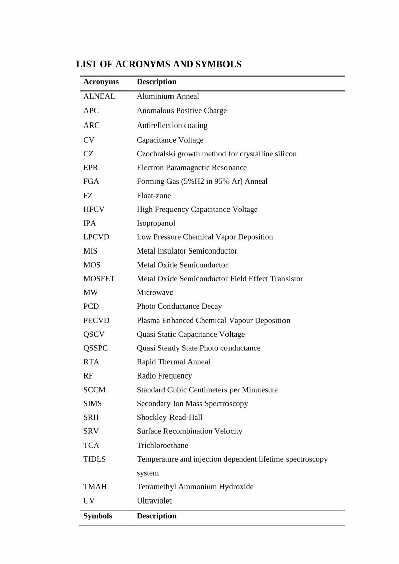
LIST OF ACRONYMS AND SYMBOLS
Acronyms Description
ALNEAL Aluminium Anneal
APC Anomalous Positive Charge
ARC Antireflection coating
CV Capacitance Voltage
CZ Czochralski growth method for crystalline silicon
EPR Electron Paramagnetic Resonance
FGA Forming Gas (5%H2 in 95% Ar) Anneal
FZ Float-zone
HFCV High Frequency Capacitance Voltage
IPA Isopropanol
LPCVD Low Pressure Chemical Vapor Deposition
MIS Metal Insulator Semiconductor
MOS Metal Oxide Semiconductor
MOSFET Metal Oxide Semiconductor Field Effect Transistor
MW Microwave
PCD Photo Conductance Decay
PECVD Plasma Enhanced Chemical Vapour Deposition
QSCV Quasi Static Capacitance Voltage
QSSPC Quasi Steady State Photo conductance
RTA Rapid Thermal Anneal
RF Radio Frequency
SCCM Standard Cubic Centimeters per Minutesute
SIMS Secondary Ion Mass Spectroscopy
SRH Shockley-Read-Hall
SRV Surface Recombination Velocity
TCA Trichloroethane
TIDLS Temperature and injection dependent lifetime spectroscopy
system
TMAH Tetramethyl Ammonium Hydroxide
UV Ultraviolet
Symbols Description

Chf(Clf) High (Low) frequency capacitance
Ci(Cs) Capacitance of insulator(semiconductor)
Dit(Ditm) Interface (midgap) state density
EF Fermi level energy
Ei Intrinsic Fermi level energy
J0e Emitter saturation current density
q Magnitude of the elementary charge
Qf Fixed charge
Qm Mobile charge
Qo Oxide charge
Qot Oxide trapped charge
Rs Sheet resistance
S Surface recombination velocity
Us Net recombination rate via surface states
Vfb Flat Band voltage
Vg Gate voltage
Φms Work function difference between metal and semiconductor
ψs Surface potential
τb Bulk lifetime
τeff Effective lifetime

Table of Contents
CHAPTER 1:Introduction ......................................................................................1
CHAPTER 2:The role of hydrogen in Si-SiO2 interface..............................7
2.1 Configurations of Hydrogen in Silicon.......................................................................8
2.2 Effect of molecular hydrogen on the Si-SiO2 interface ..............................................9
2.3 Oxides grown at different temperatures....................................................................12
2.4 Effect of atomic hydrogen on the Si-SiO2 interface..................................................12
2.4.1 Passivation and depassivation of existing Pb centres .............................................13
2.4.2 Generation of new defects......................................................................................14
2.4.4 Effect of hot electrons on Si-SiO2 interface...........................................................16
2.4.5 Effect of Ultraviolet light on Si-SiO2 interface......................................................18
2.5 Effect of post-oxidation thermal annealing on Si-SiO2 interface..............................21
2.6 Simple model for atomic hydrogen...........................................................................21
2.7 Summary ...................................................................................................................23
CHAPTER 3:Quantifying and measuring of Si surface electrical
properties…………………………………………………………………………….25
3.1 Measurement of minority carrier lifetime.................................................................26
3.1.1 Recombination mechanics .....................................................................................26
3.1.1.1 Bulk recombination.............................................................................................27
3.1.1.2 Surface recombination ........................................................................................28
3.1.2 Emitter recombination............................................................................................29
3.1.3 Effective lifetime....................................................................................................31
3.1.4 Lifetime measurement techniques..........................................................................32
3.1.4.1 Photo-conductance decay....................................................................................33
3.1.4.2 Quasi Steady State photo-conductance ...............................................................35
3.2 Measurement of Si interface properties by the Capacitance-Voltage method..........36
3.2.1 Structure and theory of ideal Metal Insulator Semiconductor ...............................36
3.2.2 Calculation of the overall electrical characteristics of silicon surfaces .................39
3.2.2.1 Calculation of insulator thickness .......................................................................41
3.2.2.2 Calculation of doping level .................................................................................41
3.2.2.3 Calculation of Flat band voltage .........................................................................41

3.2.2.4 Calculation of fixed oxide charge density...........................................................42
3.2.2.5 Calculation of interface defect density and surface potential .............................43
3.3 Measurement of paramagnetic interface defects by Electron Paramagnetic
Resonance .......................................................................................................................44
3.3.1 Paramagnetic point defects at the Si-SiO2 interface ..............................................44
3.3.2 EPR operation and calculation of Pb-type defect density ......................................45
3.4 Summary ...................................................................................................................47
CHAPTER 4:Experimental……………………………………………………..49 4.1 Hydrogenation Systems ............................................................................................49
4.2 Hydrogenation Plasma Exposure ..............................................................................50
4.3 Rapid thermal annealing ...........................................................................................52
4.4 Temperature and injection dependent lifetime spectroscopy system........................54
4.5 General sample processing........................................................................................55
4.6 Summary……………………………………………………………………………57
CHAPTER 5:Passivation effect of wet oxidation, and with
oxide/LPCVD nitride stacks on the Si-SiO2 interface………………….....59
5.1 Introduction...............................................................................................................60
5.2 Effect of low temperature oxides on the passivation of Si-SiO2 interface…………61
5.2.1 Experimental details...............................................................................................61
5.2.2 Effect of oxidation temperature on the passivation of Si-SiO2 interface...............62
5.2.3 The influence of exact processing conditions on the passivation quality of 750oC
oxide................................................................................................................................64
5.3 Effect of a phosphorous diffusion on the passivation quality of the oxide...............66
5.3.1 Experimental details...............................................................................................66
5.3.2 Effect of a phosphorous diffusion into the thin oxide on surface recombination..66
5.3.2.1 Effect on planar sample………………………………………………………...66
5.3.2.2 Effect on textured sample ...................................................................................70
5.4 Comparison of passivation effect of low temperature wet oxidation on (100) and
(111) Si-SiO2 interface....................................................................................................71
5.4.1 Experimental details...............................................................................................72
5.4.2 Effect of surface orientation and oxidation temperature........................................72
5.4.3 Thermal stability of low temperature wet oxidation (100) and (111) Si-SiO2 stack
.........................................................................................................................................73
5.4.3.1 Experimental details............................................................................................73

5.4.3.2 Stability of lifetime and J0e of samples following FGA......................................74
5.4.3.3 Stability of lifetime and J0e of samples following RTA......................................75
5.5 Passivation effect of oxide/nitride stacks on Si-SiO2 interface.................................76
5.5.1 Effect of LPCVD nitride deposition temperature on surface passivation of Si-SiO2
stack.................................................................................................................................76
5.5.2 Effect of LPCVD nitride deposition on surface passivation of Si-SiO2 stack .......78
5.5.3 Effect of subsequent LPCVD nitride deposition treatments on surface passivation
of (100) and (111) samples .............................................................................................79
5.5.4 Thermal stability of samples with oxide/LPCVD nitride stacks............................83
5.6 Summary ...................................................................................................................86
CHAPTER 6:Influence of atomic hydrogen exposure on the Si-SiO2 interface………………………………………………………………………………89 6.1 Experimental details..................................................................................................90
6.2 Background tests .......................................................................................................91
6.2.1 Effect of molecular H2 on the Si-SiO2 interface ....................................................91
6.2.2 Effect of illumination during RTA.........................................................................94
6.3 Effect of RTA on the Si-SiO2 interface following atomic hydrogen plasma exposure
.........................................................................................................................................95
6.3.1 RF power................................................................................................................95
6.3.2 MW power ...........................................................................................................101
6.3.3 Comparison of RTA results at 300oC and 400oC.................................................105
6.4 Effect of atomic hydrogen plasma exposure parameters on the Si-SiO2 interface .109
6.4.1 Influence of hydrogen plasma exposure power on Si-SiO2 interface defect
distribution ....................................................................................................................109
6.4.1.1 RF power...........................................................................................................109
6.4.1.2 MW power ........................................................................................................111
6.4.2 Influence of hydrogen plasma exposure time on Si-SiO2 interface defect
distribution ....................................................................................................................115
6.4.2.1 RF power plasma hydrogen exposure...............................................................115
6.4.2.2 MW power plasma hydrogen exposure.............................................................119
6.4.3 Influence of hydrogen plasma exposure pressure on Si-SiO2 interface defect
distribution ....................................................................................................................122
6.4.4 Optimization of the atomic hydrogen plasma exposure parameters ....................124
6.5 Effect of MW hydrogen plasma exposure and following thermal anneal on the Si-
SiO2 interface ................................................................................................................124

6.5.1 Effect of MW hydrogen plasma exposure and following thermal anneal on the Si-
SiO2 interface ................................................................................................................125
6.5.2 Influence of hydrogen plasma exposure temperature on Si-SiO2 interface
passivation.....................................................................................................................131
6.6 Effect of hydrogen plasma exposure and subsequent thermal anneal treatments on
the Si-SiO2 interface of planar (111) and textured (100) samples ................................133
6.6.1 Effect of hydrogen plasma exposure and subsequent thermal anneal treatments on
Si-SiO2 interface of planar (111) Si interface properties ..............................................133
6.6.2 Effect of hydrogen plasma exposure and subsequent thermal anneal treatments on
Si-SiO2 interface of textured (100) Si interface properties ...........................................135
6.7 Effect of atomic hydrogen and subsequent thermal annealing treatments on LPCVD
Si3N4/SiO2/Si stacks......................................................................................................137
6.8 Effect of low temperature thermal annealing on Si-SiO2 stack following MW
hydrogen plasma exposure............................................................................................140
6.9 Summary .................................................................................................................147
CHAPTER 7:Effect of corona charging, humidity, UV exposure and mineral acid on the Si-SiO2 interface………………………………………..151 7.1 Effect of corona charging and following thermal anneal on Si-SiO2 stacks...........152
7.1.1 Effect of corona charging and post corona RTA on the Si-SiO2 surface passivation
.......................................................................................................................................152
7.1.2 Detailed investigation of annealing behaviour of defects introduced by corona
charging.........................................................................................................................156
7.2 Effect of humidity on the properties of the Si-SiO2 interface.................................159
7.3 Effect of UV illumination on the Si-SiO2 surface passivation................................162
7.4 Effect of mineral acid solution on the Si-SiO2 surface passivation ........................167
7.4.1 Experimental details.............................................................................................167
7.4.2 Effect of hydrogen introduction by acid solution on Si-SiO2 interface ...............167
7.4.3 Effect of temperature and time of acid immersion on Si-SiO2 interface .............171
7.5 Summary .................................................................................................................174
Summary and further work ................................................................................177
List of Publications.................................................................................................181
Bibliography .............................................................................................................183


Chapter 1: Introduction 1
CHAPTER 1
Introduction
Photovoltaics, the direct conversion of sunlight into electricity using solar cells, is
recognized as one of the most promising options for a sustainable energy. Today,
single- or multi-crystalline silicon wafers dominate the present photovoltaic market and
this market dominance is likely to continue at least until the next decade. The solar
industry needs to reduce production costs of solar modules while, at the same time,
improving the energy conversion efficiency of the solar cell. For silicon wafer-based
solar modules, large cost savings can come from reducing silicon wafer thickness, since
silicon feedstock, crystallization, and wafering make up 33% of the direct
manufacturing costs. As cell thickness is reduced and efficiency increases, the surfaces
of the solar cell become increasingly important. The challenge is then to obtain thin,
high efficiency silicon solar cells with very well passivated surfaces.
The surface recombination velocity S at the semiconductor surface measured in
units of cm/s can be defined as [1]
ss nSU ∆•≡ (1-1)
Chapter 1: Introduction 2
where ∆ns is the excess minority-carrier concentration at the surface, Us the net
recombination rate via surface states, which is determined by carriers concentrations,
capture cross sections for carriers and the surface state density.
Based on equation (1-1), surface recombination velocity depends on the density of
interface defects, their properties (capture cross sections, to a less extent energy levels)
and the concentration of carriers at the surface.
Since 1960s, the Si-SiO2 structure has been one of the most intensively studied
systems in the realms of materials and condensed matter physics. The main driver for
this intense effort is the critical role of the structure in the metal-oxide-semiconductor
field effect transistor (MOSFET), which dominates contemporary integrated circuit (IC)
technology [2]. During the past decades, the Si-SiO2 interface has become the most
intensively investigated semiconductor-insulator system. In the photovoltaic community,
the standard method for the passivation of Si surfaces-both diffused and non-diffused- is
the thermal oxidation at high temperature (~1000oC) [3]. For non-diffused Si surfaces,
thermal SiO2 provides excellent surface passivation on high-resistivity (>100Ω.cm) n-
and p-type Si wafers, as demonstrated by effective surface recombination velocity Seff
values below 10cm/s. For low substrate resistivity (~1Ω.cm) the passivation quality
depends on the doping type. Thermal SiO2 is also very effective in passivating diffused
Si surfaces. Furthermore, due to the large surface doping level (Ns≥5x1018cm-3), the
band bending at the surface is virtually independent of the operating condition of the
sample and hence the surface recombination velocity at diffused Si surfaces can be
treated as being independent of the bulk injection level ∆n.
Although thermally grown SiO2 films provide very good surface passivation on
silicon wafers, with regards to fabrication of solar cells they feature two severe
drawbacks [4]: (ⅰ)they do not provide efficient reduction of reflection losses because
of their small refractive index of 1.46 and (ⅱ)their fabrication requires high processing
temperatures and relatively long processing times which will bring numerous problems
such as cost and throughput considerations, degradation of bulk lifetime especially for
multi crystalline silicon and etc. In order to eliminate the above problems associated
with the high temperatures during the thermal oxidation of silicon, significant effort has
been devoted in the past to the development of low-temperature surface passivation
schemes. The most successful of these approaches has turned out to be the formation of
SiN films by means of the low-temperature Plasma Enhanced Chemical Vapor
Deposition (PECVD). PECVD SiN combines a number of desirable features for the

Chapter 1: Introduction 3
achievement of high-performance solar cell [5]:(ⅰ)high interface charge density
leading to high concentration of carriers at the semiconductor surface, (ⅱ)long-term
stability of these charges at elevated temperatures, (ⅲ)relatively low interface defect
density of electrically active defects, (ⅳ)good antireflection (AR) coating properties
with the refractive index in the range of 1.7-2. The SiN film properties can be varied
widely depending on deposition parameters such as deposition temperature, pressure,
plasma power, gas flow rate and gas ratio. All deposition parameters strongly affect the
surface recombination velocity as well as the stability of the SiN film against the UV
exposure, therefore there is significant room to optimise the properties for a given
application. It should be emphasized that plasma SiN films are of an amorphous
structure and contain large amounts of atomic hydrogen which can passivate bulk and
interface defects. However, as discussed above, when PECVD SiN is deposited directly
on silicon, a very thin interfacial SiOx film (<2nm), which grows on the silicon surface
prior or in the initial stages of nitride deposition, is converted into an oxynitride film.
This oxynitride film is not a mixture of SiO2 and Si3N4 clusters, but of Si-O and Si-N
bonds blended on an atomic scale, and is believed to be inferior in terms of its electronic
properties to the Si-SiO2 interface [4].
The Si-SiO2 interface is still very important in crystalline silicon solar cell devices.
In addition to the excellent surface passivation it affords, the research of the properties
of Si-SiO2 interface is also driven by a few factors. Firstly, oxide/PECVD silicon nitride
stacks are under active investigation within photovoltaic community and a low surface
recombination velocity of nearly 10cm/s on 1.25Ω.cm p-type (100) silicon surface has
been reported [6]. Secondly, even when PECVD nitride is used, interface is an
oxynitride converted from a very thin SiOx film. Hence, it can be expected that the
actual interfacial region on silicon wafers covered by a PECVD SiNx film is rather
similar to the one found at the thermally grown Si-SiO2 interface [7]. Thirdly, it has
been known that excellent surface passivation can be obtained by thin Al2O3 films
prepared by plasma-assisted atomic technique and it was verified that an interfacial
oxide layer of about 1.5nm is present between the silicon and Al2O3 as a result of the
deposition process [8]. Last but not least, rear surface passivation is becoming
increasingly important in crystalline silicon solar cell technology and thermally grown
silicon dioxide layers meet all major requirements to be suitable for it: good surface
passivation, good rear reflectance, and thermal stability in solar cell production
processes. Only the process throughput and cost and the possible degradation of the
Chapter 1: Introduction 4
solar cell precursors seem to be the major and crucial problems [9]. Therefore, the
properties of the Si-SiO2 interface continue to be of great interest for solar cells
applications.
From the above overview, it is natural to expect that PECVD SiNx/SiO2/Si stacks
will display lower surface recombination rates and better thermal stability than PECVD
SiNx /Si structures. That is because, on the one hand, the thin layers of thermally grown
SiO2 is known to be the best technique for passivating the Si surface and Si-SiO2
interface containing a lot of recombination centres caused by the dangling bonds can be
effectively passivated by atomic hydrogen. In the above applications, usually the thin
SiO2 layer is grown at lower temperatures (900oC or below) for short time to get about
10nm thickness [10]. On the other hand, PECVD SiNx films contain high density of
hydrogen (20-25% depending on deposition conditions [11, 12]). This hydrogen will
release (in atomic and/or molecular form, depending on the SiNx film properties)during
the following high temperature solar cell processing step and then diffuse into the
silicon bulk, where it can passivate both deep and shallow level defects, including
dopant atoms [13-15]. Actually, a novel SiO2/SiN double-layer antireflection coating,
which greatly improves the efficiency and performance of solar cell, has been
developed [16]. Furthermore, it is found that SiO2/SiN stack passivation quality,
following either low or high temperatures annealing, is superior to the counterpart
individual films [17].
It is well known that hydrogen readily attaches to broken chemical bonds in
semiconductors, thereby repairing damage and eliminating detrimental electronic states
from the energy bandgap. Technological interest in the study of hydrogen in the
semiconductors arises from two diametrically opposed motivations. Firstly hydrogen
can be unintentionally introduced into the material during any phase of semiconductor
processing, such as crystal growth, deposition or growth of over-layers, wet or dry
chemical processing, and even device operation. On the other hand, hydrogenation can
also be incorporated as a deliberated processing step in the fabrication of semiconductor
devices for the purpose of passivating dopants and defects. In either case, a fundamental
understanding of the properties of hydrogen in semiconductors will provide the most
vigorous basis for addressing the technological implications and realizing the
technological opportunities of hydrogen in semiconductors [18].
The role of molecular hydrogen at the Si-SiO2 interface is relatively well
understood, especially through the studies by Stesmans et al [19-23]. However, the
reaction of atomic hydrogen with the Si-SiO2 interface has not been investigated in as
Chapter 1: Introduction 5
much detail, despite its important role in surface passivation. An example is the so-
called alneal (aluminium anneal), resulting in excellent surface passivation (superior to
that obtained by a forming gas anneal) for Si-SiO2 structures. This is often attributed to
the generation of atomic H during the alneal [24]. However, this view is not supported
by the work by Stesmans and Cartier [19, 25], as well as Jin et al [26].
The aim of the thesis is to explore the properties of lower temperature oxides in
comparison with high temperature oxides, to improve the understanding of the
interaction of hydrogen, especially atomic hydrogen, with the Si-SiO2 interface, and to
determine to what extent atomic hydrogen may be responsible for commonly observed
degradation of Si-SiO2 interface following the application of high electric fields,
humidity exposure, UV exposure and mineral acid immersion.
Thesis outline
In chapter 2, a review of the properties and effects of hydrogen, including
molecular and atomic on Si-SiO2 interface is presented. The basic characterization
techniques used in this thesis are described in chapter 3, and then the details of
processing equipments and general sample processing are demonstrated in chapter
4. In chapter 5, effect of wet oxidation, and with oxide/LPCVD nitride stacks on
Si-SiO2 interface is discussed. In chapter 6, results for applying atomic hydrogen to
Si-SiO2 interface and following different thermal treatments are presented and
discussed. Finally, effects of corona charging, humidity, Ultraviolet (UV) exposure
and mineral acid solutions on Si-SiO2 interface are investigated in chapter 7. These
experiments cover both planar and textured (111) and (100) surfaces.

Chapter 1: Introduction 6
Chapter 2: The role of hydrogen in the Si-SiO2 interface 7
CHAPTER 2
The role of hydrogen in the Si-SiO2
interface
It has long been known or suspected that hydrogen plays a major role in numerous
useful and harmful phenomena in the Si-SiO2 system. Although certain specific
situations have been fairly well studied, many have not.
The incorporation of atomic hydrogen into crystalline, polycrystalline or
amorphous semiconductors causes significant changes in both the electrical and optical
properties of these materials. The principal interest in hydrogen in crystalline
semiconductors occurs because of its ability to passivate (render electrically inactive)
dangling bonds or defects. Hydrogen can be introduced into semiconductors during
crystal growth, by direct implantation, by exposure to hydrogen-containing plasma, or
by chemical reaction at the surface [27]. In many cases its incorporation into crystalline
semiconductors is unintentional, and can cause changes in the electrically active dopant
profile in the near-surface region.
Due to its ability to deactivate both shallow and deep impurities in one of the most
technologically important semiconductors, silicon, the role of hydrogen in silicon has
attracted wide interest. Hydrogen will also passivate many deep defects in other
elemental and compound semiconductors [28], as well as surface dangling bonds in
Chapter 2: The role of hydrogen in the Si-SiO2 interface 8
both amorphous and single crystal silicon [29] and trivalent Si defects at Si-SiO2
interfaces [30].
2.1 Configurations of Hydrogen in Silicon
At the present time there is a consistent picture of the states of hydrogen within the
lattice for Si. In this section knowledge of these different forms of hydrogen will be
detailed, which is based primarily on a series of calculations from the Albany group
[31-33], in which they think there are three states of hydrogen in Si at low temperatures
[13]:
(1) Bound to a dangling bond at a defect site. These give rise to the multiplicity of
Si-H stretching modes observed by infrared absorption in the frequency range 1800-
2300cm-1. This site has the lowest potential energy for any of the states of hydrogen.
(2) Molecular hydrogen (H2) which is the stable configuration in the absence of
defect sites to which the hydrogen can bond. Molecular hydrogen is electrically and
optically inactive, and essentially immobile at low temperatures (<500oC). The extra
stability of the molecular form over atomic hydrogen at low temperatures translates to a
total dominance in the relative concentrations in defect-free Si.
(3) Atomic hydrogen (H) occupies the lowest energy site for unbound hydrogen.
The diffusivity of atomic hydrogen is high even at room temperature as it migrates
through the lattice at the cost of a small energy barrier (0.3eV) [34, 35]. It is the state
responsible for the passivation of dangling bond electrical activity. The reason why little
direct observation of the electrical activity has been made for atomic hydrogen is that it
tends to either bond at a defect site, or coalesce into molecules [32].
These three forms of hydrogen are in equilibrium amongst themselves. At low
temperatures, for example, the bonded forms (Si-H and H2) predominate, and hence
hydrogen is relatively immobile. At high temperatures the atomic form dominates as the
bound forms break up, and then the effective diffusivity is high. A summary of the
properties of the three states of hydrogen in Si is given in Table 2.1 [32].

Chapter 2: The role of hydrogen in the Si-SiO2 interface 9
Table 2.1 Calculated properties of three states of hydrogen in c-Si [32] Si-H H2 H Potential energy [eV] -14~-15.8 -26.6 -12.5 Heat of solution [eV] - 1.7 1.65
(exp.1.87) Activation energy for diffusion [eV]
- 2.7 0.32 (exp.0.5~1.2)
Dissociation energy [eV]
1.5~3.3 1.6 -
2.2 Effect of molecular hydrogen on the Si-SiO2
interface
It has long been recognized that, following thermal oxidation, the crystalline silicon
atoms at the Si-SiO2 interface bond to oxygen atoms of the SiO2. Nevertheless, up to
approximately 0.5% of the crystalline interfacial atoms are not bonded to oxygen atoms
and give rise to a specific dangling bond type of defects, Si3≡Si·, called the Pb center. In
this notation, the three horizontal lines represent the three bonds to bulk silicon atoms
(the Si3), and the · represents the fourth, unpaired valence electron of the silicon atom
(the so called dangling bonds). In the neutral charge state, this interface defect is
observable with electron paramagnetic resonance (EPR). The paramagnetism of this
defect arises from an unpaired electron located in a sp3[111]-like hybrid orbital localized
on the defect silicon atom [36]. In general, there is only one type of paramagnetic defect,
namely Pb centre is observed on (111) Si interface, while two distinct paramagnetic
defects called Pb1 and Pb0 are observed on (100) Si interface. The Pb0 (100) is reasonably
attributed to Si3≡Si· on the (100) face while Pb1 (100) tentatively consistent with
Si2O≡Si· centres [36]. The disposition of Pb centres on the three principal Si faces in
shown in figure 2.1[2].

Chapter 2: The role of hydrogen in the Si-SiO2 interface 10
Figure 2.1. Structure of Pb centres on Si wafers of three major orientations [2].
These Pb defects are believed to be the dominant interfacial charge traps that make
this as-grown Si-SiO2 system less than ideal in device applications. In order to minimize
the effects of charge trapping at such defects, much research has been done during last
decades. In most experiments the Si-SiO2 stacks are exposed to molecular hydrogen to
passivate, or annealed in vacuum to depassivate samples, the idea being that the
hydrogen will chemically bind to and passivate these defects. Brower [36, 37]
researched the kinetics of H2 of Pb centres and the dissociation kinetics of hydrogen-
passivated Pb defects on the (111) Si-SiO2 interface. The mechanism is simply
summarised in the following reactions:
Pb + H2 → PbH + H (2.1)
PbH → Pb+ H (2.2)
H2 → H + H (2.3)
PbH + H → Pb + H2 (2.4)
Pb + H → PbH (2.5)

Chapter 2: The role of hydrogen in the Si-SiO2 interface 11
Where PbH represents a passivated Pb centre. Brower’s results indicated that the
molecular hydrogen chemistry of Pb centres is dominated by three thermochemical
effects. The first is that Pb centres appear to be stable under vacuum annealing to
temperatures of at least 850oC. The second is that Pb centres can be passivated with
molecular hydrogen to form PbH centres. The third is that passivated PbH centres
dissociate in vacuum for temperatures in excess of 550oC.
Stesmans et al. conducted further detailed experiments to obtain a better
understanding of the Pb centre at the Si-SiO2 interface [38]. At first, they accurately
determined the density of interfacial (111) Pb centres (Si3≡Si· defects, passivated or not)
to be (11.4±0.6)x1012cm-2 on all (111) Si-SiO2 interfaces prepared by oxidation in dry
O2 at 920-1000oC. The Pb centres were found to account for all electrically active fast
interface states. Stesmans et al. then extended and revised Brower’s work by using more
accurate and correct EPR practice [19-21] for (111) and (100) samples respectively. The
results indicate that passivation with molecular H2 of all Pbx interface defects in either
thermal (111) or (100) Si-SiO2 over extended temperature and time ranges show a non-
exponential decay of the unpassivated Pb centre density with time. The results were
explained by postulating a Gaussian spread in the activation energy Ef for the
passivation of Pb centres. The mean activation energy for all Pbx centres are similar and
in the range of 1.51 to 1.57eV and the Gaussian spread σEf is in the range of 0.06 to
0.15eV for all Pbx centres.
Stesmans [23] also analysed the simultaneous action of passivation and dissociation
during thermochemical interaction of Pb defects with molecular hydrogen at the (111)
Si-SiO2 interface. A unified description is attained through solution of the simultaneous
set of the first-order rate equations describing passivation and dissociation, under the
restriction that the H2 concentrations at the interface and in the ambient are continuously
equal and inclusion of the spreads σEf and σEd in activation energies. Focusing on the
passivation in 1atm H2, Stesmans found that optimum passivation can be achieved in
the range of 400-430oC for 10-60 minutes. Stesmans also pointed out that the combined
chemical reactions 2.1 and 2.2 make the Pb defect a catalyst for H2 dissociation, in
which both the passivation and depassivation process lead to the emission of atomic
hydrogen.
When optimally passivated, the density of unpassivated Pb-type defects can become
very low, with a density in the range (2-10)x109cm-2 of residual interface traps detected
electrically in state-of-the-art passivated Si-SiO2.
Chapter 2: The role of hydrogen in the Si-SiO2 interface 12
2.3 Oxides grown at different temperatures
It has been presented in previous chapter that oxide/PECVD silicon nitride stacks
are under active investigation within photovoltaic community and usually the thin
tunnel oxide is thermally grown at lower temperatures (900oC or below). Aberle et al. [4]
found that there is an enormous increase in the effective lifetime by increasing the
oxidation temperatures during the range of 500-800oC. Schmidt et al. [39] investigated
the thin thermal SiO2/PECVD SiNx stacks. The oxides were grown in an
oxygen/trichloroethylene ambient using a conventional quartz furnace at 900oC with
thickness range of 5-25nm. The results showed that there was an enormous increase in
lifetime from 5-8µs to 1-2ms after the deposition of 60nm SiNx layers on top of the SiO2.
Rohatgi et al. [10] investigated the thin rapid thermal oxide (RTO)/PECVD SiNx stacks.
This rapid thermal oxidation at 900oC for 150 seconds resulted in an oxide with
thickness of about 8-10nm on diffused surface and 6nm on undiffused surface. The
results showed the optimum passivation scheme consisting of a thin RTO with PECVD
SiNx layer followed by a very short 730oC anneal can significantly reduce the emitter
saturation current density and the back surface recombination velocity. Furthermore,
this double-layer RTO+SiNx passivation is relatively independent of the deposition
conditions (direct or remote) of the SiN film and is more stable under heat treatment
than SiNx or RTO alone.
2.4 Effect of atomic hydrogen on the Si-SiO2 interface
The role of molecular hydrogen at the Si-SiO2 interface is relatively well
understood, especially through the studies by Stesmans and co-workers [19-23].
However, the reaction of atomic hydrogen with the Si-SiO2 interface has not been
investigated in as much detail, despite its important role in surface passivation. Very
often it is atomic H that interacts directly with the Si-SiO2 interface, rather than
molecular H2. For example, it is atomic H rather than H2 that is usually released from
PECVD nitride films during high temperature thermal treatments, such a contact firing.
Another example is the alneal, resulting in excellent surface passivation for Si-SiO2
structures. This is often attributed to the generation of atomic H during the alneal [24].
Therefore it is important to understand the interaction of atomic hydrogen with Si-SiO2
as well.

Chapter 2: The role of hydrogen in the Si-SiO2 interface 13
2.4.1 Passivation and depassivation of existing Pb centres
Cartier et al. carried out numerous investigations into the effect of atomic hydrogen,
produced by remote PECVD reactor, at the Si-SiO2 interface at room temperature [25].
In their experiments, samples were oxidised in dry oxygen at 900oC and exposed to
atomic hydrogen by using remote microwave hydrogen-plasma system. The EPR
technique was used to investigate the Pb centre density at Si-SiO2 interface. These
experiments showed that atomic hydrogen at the (111) Si-SiO2 interface both
depassivates and passivates silicon dangling bonds simultaneously at room temperature
according to the reactions (2.4) and (2.5). This was indicated by an increase in the EPR
signal for paramagnetic Pb centres for as-grown, hydrogenated Si-SiO2 sample and a
decrease in the signal for paramagnetic Pb centres for initially dehydrogenated samples
following atomic hydrogen exposure. The fact that the EPR signal from Pb centre was
reduced on initially depassivated samples shows that atomic H can passivate Pb centres.
On the other hand, the fact that the signal increases on initially passivated sample shows
that atomic H can depassivate and that the passivation of atomic H is not as effective as
that of molecular H2. (Note that, in their experiments, the samples did not receive a
forming gas anneal or other anneal in molecular hydrogen following oxidation. Such an
anneal, had it been carried out, would not have changed the experimental results since
no EPR signal was detected after oxidation, and a forming gas anneal would, if anything
result in a further lowering of the unpassivated Pb centre density, based on the work of
Stesmans et al. Furthermore, in order to prove that the low saturation Pb density value of
3.0±0.5x1011cm-2 is actually the result of simultaneous passivation and depassivation of
silicon dangling bonds, a sample with high Pb density (2.4x1012cm-2) following high
temperature (700-800oC) vacuum annealing received a long atomic hydrogen exposure
for about 120 minutes. After that, the Pb density in this kind of depassivated sample
decreased to a value of 4.5±0.5x1011cm-2, which is very close to that measured after
atomic hydrogen exposure of the thermal as-grown passivated sample.
The important result, therefore, is that the final unpassivated Pb density following
atomic hydrogen exposure reaches a steady state value that is, to a first order,
independent of initial passivation state of the Pb centres.
In addition to (111) samples, Cartier et al. also investigated the reaction of atomic
hydrogen with defects at the (100) Si-SiO2 interface by EPR [40]. The experiment
conditions are identical as above (111) samples. Their results showed that the two
paramagnetic defects at the (100) interface, Pb0 and Pb1, respond in a similar way to

Chapter 2: The role of hydrogen in the Si-SiO2 interface 14
atomic hydrogen as the Pb centre at the (111) interface. However, the two kinds of Pb
defects display quantitative difference in behaviour. It is found the Pb0100 centre is
produced more readily than Pb1100
and is also much harder to passivate by atomic
hydrogen. This means that the Pb0100 is the dominant defect at the (100) Si-SiO2
interface and it is chemically not equivalent to Pb111. On the other hand, there is strong
evidence to suggest that Pb111 and Pb1
100 are similar to each other (ie have the same
backbonding arrangement) and different from Pb0100.
2.4.2 Generation of new defects
Cartier et al. also discovered that atomic H can generate new interface defects [25].
The C-V technique was used to compare the interface state density (Dit) at midgap with
the paramagnetic Pb density (from EPR) at the (111) Si-SiO2 interface. Samples
received dry oxidation followed by atomic H exposure for different times. They found
that mid-gap interface state density (Ditm) of the as-grown sample increased linearly
with atomic hydrogen dose at least up to a density of 1x10¹³eV-1cm-2 with no indication
of saturation. However, the Pb density increased at a roughly ten times smaller rate than
the density of electrically active defects and saturated at a value of about 3x1011cm-2.
The authors rule out the possibility that the difference is due to the difference in
substrate resistivity or oxide thickness by measuring the Ditm values on samples with
different oxide thickness and resistivity but getting close Ditm values. This kind of
phenomenon was also observed at (100) Si. Similar to the (111) interface in which the
Pb111 centre could account for only a fraction of the atomic hydrogen-generated interface
states, paramagnetic defects (Pb0 and Pb1) likewise could not account for all of the
electrically active defects at the (100) interface. The above results suggest that atomic
hydrogen introduces defects at the Si-SiO2 interface which are not EPR-active.
In subsequent more detailed studies, Cartier et al. studied the generation of interface
states in atomic hydrogen plasma exposure over a wide range of oxide thickness grown
on various p- and n-type substrates using the C-V technique [41]. The results indicated
that, firstly, Dit increased linearly with the atomic H-dose up to values of 1x10¹³eV-1cm-
2 for both (111) and (100) interface. Also, the results showed that the (111)-interface
degrades approximately 2.5 times faster than (100)-interface, independent of the oxide
thickness. The reason behind this is possibly due to a higher precursor density at the
(111) interfaces. Secondly, the authors found that the generation rates on p-type
substrate are systematically higher compared to n-type samples. This might be related to
Chapter 2: The role of hydrogen in the Si-SiO2 interface 15
a dependence of the interface-state generation rate on the Fermi level at the Si-SiO2
interface. Thirdly, from Dit distributions across the band-gap with different atomic
hydrogen dose (both n- and p-type samples), the authors again found these distributions
are strongly asymmetric respect to mid-gap of the band-gap and are not compatible with
those reported Pb dangling bonds. Again, the results provide evidence that the majority
of the electrically detected defects are not related to the well known EPR signal for Pb Si
dangling bonds.
Cartier et al. also studied interface defect formation caused by introducing atomic
hydrogen into the gate oxide of MOSFETs and compared the results to introducing it
into a gate-free thermal oxide [42]. MOSFETs with the edges of the gate oxide at the
source and drain exposed to the ambient were placed downstream of atomic hydrogen
plasma. Baffles prevented UV rays from the plasma from reaching the device. Interface
traps in the MOSFETs were measured by charge pumping and interface defect
formation was examined by high-low C-V measurements performed with a mercury
probe. They observed that both types of samples exhibit the same energy distribution of
interface traps from the C-V results. While atomic hydrogen produces the same defects
in both the MOSFETs and bare thermal oxides, the diffusion pattern of the atomic
hydrogen through the two types of samples is very different. For the bare thermal oxide,
the interface trap generation rate decreases with oxide thickness, tox, as approximately
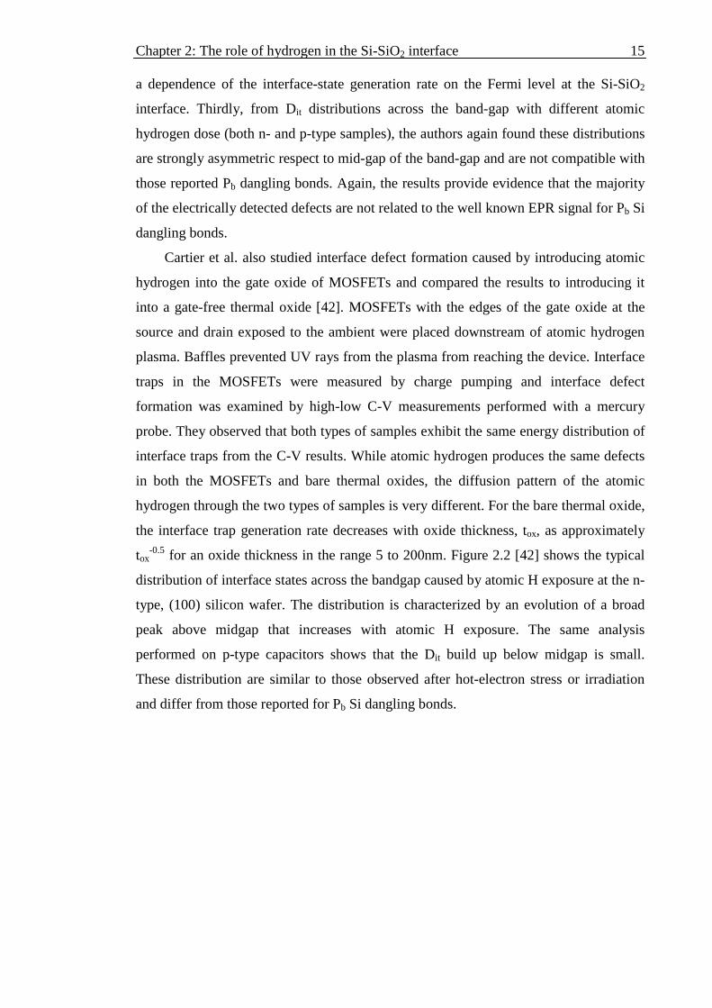
tox-0.5 for an oxide thickness in the range 5 to 200nm. Figure 2.2 [42] shows the typical
distribution of interface states across the bandgap caused by atomic H exposure at the n-
type, (100) silicon wafer. The distribution is characterized by an evolution of a broad
peak above midgap that increases with atomic H exposure. The same analysis
performed on p-type capacitors shows that the Dit build up below midgap is small.
These distribution are similar to those observed after hot-electron stress or irradiation
and differ from those reported for Pb Si dangling bonds.

Chapter 2: The role of hydrogen in the Si-SiO2 interface 16
Figure 2.2. Dit distribution for the bare thermal oxide measured by high-low CV in a Hg
probe after various atomic hydrogen dose exposure [42].
2.4.3 Formation of anomalous positive charge
Besides producing the interface defects, Cartier et al. also found atomic hydrogen
exposure can lead to the formation of anomalous positive charge (APC) near the Si-
SiO2 interface at room temperature by analysing interface defects and oxide charge
through C-V measurements [43]. After thermal oxidation (with oxide thickness of about
100nm) and forming gas anneal (FGA), the sample received a few minutes room
temperature atomic hydrogen exposure. A simultaneous increase of the high-frequency
C-V stretch-out and hysteresis caused by atomic hydrogen exposure can be observed,
with the hysteresis of the high frequency curve increasing from less than 20mV to
several volts. It is possible that the defect responsible for the APC is similar in structure
to the interface defect that can be measured from the C-V curves, but with much longer
charging/discharging times (typically in the order of seconds to hours). The charge state
of the defect can be cycled between positive and neutral by the gate voltage.
2.4.4 Effect of hot electrons on Si-SiO2 interface
Hot-electron effects are known to degrade the performance of Si-SiO2-based
electronic devices. It is known that hot-electron stress liberates atomic hydrogen from
within the oxide (or from the oxide/gate-metal interface), and some of this atomic

Chapter 2: The role of hydrogen in the Si-SiO2 interface 17
hydrogen will diffuse to the Si-SiO2 interface to react with interface defects. Cartier et al.
observed that the hot electron degradation shows similar processing dependences as the
atomic H-induced degradation at both (111) and (100) Si-SiO2 [25, 40].
Generally, there are two main degradation modes that are observed to be
responsible for the degradation. These two mechanisms are the phenomena of “trap
creation” and “impact ionization” produced by electrons with energy exceeding about
2eV [44] and 9eV [45], respectively. For the trap creation process, electrons with energy
greater than 2eV release hydrogen from defect sites near the anode interface (metal or
gate-SiO2 interface). This mobile species can then move to the cathode-oxide interface
(Si-SiO2) where it produces interface states and a distribution of oxide electron traps
near this interface. This process is thermally activated, has a weak oxide thickness
dependence (for films over 10nm), and is observed in an electric field as low as
1.5MV/cm. For impact ionization process, mobile holes produced in the oxide bulk near
the anode move under the applied field to the Si-SiO2 interface where some are trapped
in oxygen vacancies. Some of the injected electrons from the Si recombine with these
trapped holes producing interface states and traps near the Si. This process is weakly
dependent on lattice temperature, has a strong oxide thickness dependence up to about
50nm, occurs only at fields exceeding 7MV/cm, and is measurable at injected fluencies
as low as 1x10⁻⁶C/cm2.
Similar to the remote hydrogen plasma experiments in which reactions (2.4) and
(2.5) can occur simultaneously and reaction (2.5) is more efficient at room temperature,
Cartier et al. showed that these same reactions may also occur during hot electron stress
in MOS capacitors [46]. In their experiments, silicon dioxide films (20nm) were
thermally grown at 850°C on n- and p-type (111) oriented silicon (40-60Ω.cm).
Dehydrogenation was realised by using vacuum annealing at 700oC for 2 hours.
Quasistatic and high frequency C-V measurements were done on dehydrogenated MOS
stacks. Their results indicated that, during hot electron stress at certain electron fluence,
pre-existing unpassivated Pb centres are passivated, indicated by the significant
reduction of two capacitance peaks position nearly symmetrically about mid-gap in the
Dit distributions, in which the area under each peak agrees well with the Pb density
measured by EPR. However, there is a clear increase of Dit distribution under the same
processing conditions at the same time. Following a 180oC anneal, the interface defects
density decreases again and almost recovers to the level of dehydrogenated control
sample. Secondly, by analysing the dependence of [Pb] and mid-gap Dit on electron
fluence, their results indicated that, with increasing electron fluence, there was a gradual
Chapter 2: The role of hydrogen in the Si-SiO2 interface 18
decrease in unpassivated [Pb] until a stable-state density was reached, but a linear
increase with no indication of saturation during the whole range of electron fluence for
mid-gap Dit, showing the simultaneous Pb passivation and the generation of new
interface defects during hot electron stressing. Combined with earlier experiments on
the Pb generation due to hot electrons [47, 48], these results demonstrate a strong
analogy between the degradation during hot electron stress and the degradation in a
remote hydrogen plasma, providing a firm basis for the hot-electron-induced hydrogen-
release model for interface degradation.
DiMaria et al. [44] found that hot electrons in SiO2 can cause the generation of
small capture cross-section traps (≤1x10-18cm2) in oxide layers at injected charge
fluences≥1C/cm2 and fields≥1.5MV/cm. In their experiments, poly-silicon gated n-
channel MOSFETs on p-type (100) silicon samples were used. The gate oxides were
grown at 1000oC in O2 with 4.5% HCl. Optically induced hot electron injection from
the Si substrate was used on the sample. Their results show that, at first, if the electric
field magnitude is more than 1.5MV/cm, bulk oxide electron traps are proportional to
the injected charge and the electric field applied on the SiO2 layer by considering
voltage shifts deduced from I-V characteristics. Moreover, the high frequency C-V
characteristics indicated that both the density of positive charge and interface states at
the Si-SiO2 interface show a similar trend to that of the bulk oxide electron traps. The
generation of these sites was attributed to the liberation of some forms of hydrogen
which pile up near the Si-SiO2 interface and lead to both the bulk negative trapped
charges, interface positive charges, and the interface states observed. For both thin and
thick oxides, there is a threshold for trap creation of about 2.3eV by the hot electrons in
the oxide conduction band.
2.4.5 Effect of Ultraviolet light on Si-SiO2 interface
In 1985, Blumenstock and Hezel [49] reported a surface state creation by UV
radiation. They found that interface states at the Si-SiO2 interface are generated by UV
irradiation after plasma silicon nitride deposition onto the thermal silicon oxide. The
generation occurs at photon energies greater than 4.3±0.2eV even at nearly zero oxide
fields.
Gruenbaum et al. [50] discussed the degradation of single crystal silicon point-
contact solar cells after UV exposure. Carrier lifetime and density of interface traps
were measured by a contactless inductance coil and high-low frequency C-V

Chapter 2: The role of hydrogen in the Si-SiO2 interface 19
measurement respectively. UV exposures were done with either concentrated sunlight,
mercury lamp or a xenon arc lamp. The experiment results show that there is an
efficiency loss for the point contact solar cells with increasing UV exposure time. These
cells had a textured front surface with a Trichloroethane (TCA) oxide as surface
passivation. The efficiency dropped quickly in the first three hours and then the
degradation slowed during the total eight hours exposure time. Moreover, some MOS
capacitors were made to directly measure the density of interface traps. These devices
were exposed to either the mercury lamp or to 50W/cm2 of concentrated sunlight (5-
hour exposure to sunlight at 50W/cm2 had a similar effect to a 30-minute exposure
under the mercury lamp). The effects of the two types of exposure were very similar:
there was a rise in surface states, and the surface charge became significantly more
negative after the UV exposure. Meanwhile, the Dit distribution curves for these two
devices were identical within the error of the measurement, and the charge density was
also approximately the same. These results suggested that the interface damage caused
by concentrated sunlight is of a similar kind to that caused by 254nm UV light. In
addition, the effects of processing variables were also investigated by the authors. FZ,
(100), high resistivity, n-type wafers were used for lifetime measurements. Parameters
including two different silicon surface (polished and texturized), three different
oxidations (with TCA, without TCA, and without TCA but with a HF treatment), and
two different anneals (forming gas anneal and aluminium anneals) were investigated.
The results showed that texturization, TCA oxidations, and aluminum anneals all
contribute to the instability of the Si-SiO2 interface. The HF treatment makes no
difference for the polished wafers, but may make texturized wafers somewhat less
stable. Lastly, they attempted a different processing technique to make more stable
passivations and prevent UV degradation by using phosphorous diffusions. Reasonably
good resistance to ultraviolet can be created by putting a phosphorous diffusion at the
surface, and can be improved further by stripping off the deposited oxide after the
diffusion and regrowing a dry thermal oxide.
Zhong et al. [51] also reported similar results by using gate-free Si-SiO2 stacks. It
was found that the effective lifetime in silicon substrate with thermal oxide decreases
dramatically after 4.9eV UV irradiation but remains almost unchanged after exposure to
4.2eV photons. The lifetime degradation is correlated with the generation of interface
traps, and explained by the authors with the hot electron induced hydrogen
redistribution model, in which an electron in the oxide conduction band needs an extra
energy of 2eV to release hydrogen atoms trapped in the oxide. Since the samples used

Chapter 2: The role of hydrogen in the Si-SiO2 interface 20
are gate-free, it is suggested that the oxide itself can be at least a part of the hydrogen
source.
Lee et al. [52] also reported the effect of UV irradiation on the minority carrier
recombination lifetime using a laser-microwave photo-conductance method for wafers
oxidized at 700, 900, and 1000°C respectively and for different oxidation times at these
temperatures. A UV chamber with three 8W UV lamps at the top and bottom of the
chamber was used to illuminate the wafer from both sides with UV wavelength
253.7nm. For wafers oxidized at 1000°C (oxide thickness>10nm), the lifetime was
found to decrease with UV irradiation and then saturate. The saturation values increased
with the thickness of oxide, which indicates that for thicker oxide, the interfacial layers
are more resistant to photogeneration of surface trapping centres by UV irradiation. For
wafers oxidized at 700oC (oxide thickness<10nm) and 900oC (oxide thickness between
6.5 and 42.5nm), the lifetimes could continually increase or decrease or initially
decrease and then increase with UV irradiation, depending on the oxide thickness. It
was suggested that, all the effective lifetime changes with UV irradiation could be
attributed to surface trap generation and annihilation activities. However, a change in
the oxide charge due to the UV irradiation could also produce changes in lifetime.
Meanwhile, they also proposed a mathematical model which describes the effect of UV
irradiation on the effective lifetime and surface potential of silicon wafers [53]. Five
variable parameters including total trap density and charge density (oxide and interface)
and maximum O2- charge density on the oxide surface etc are used in the model. This
simple model assumes the presence of two species of interface traps, which interchange
their densities. By comparing the simulations and experimental data for either lifetime
or surface potential to UV illumination time, the simulations using the model are in
good agreement with the experimental data.
McIntosh et al. [54] investigated the effect of surface charge on defect generation at
the Si-SiO2 interface by ultraviolet radiation. It was found that the presence of positive
charge on the surface of oxidised silicon significantly reduced the photon energy
required for both electron injection and defect generation at the Si-SiO2 interface under
UV irradiation. Defect generation was found to occur with photons of considerably less
energy than previously reported, with evidence that photons with energy below 3.66eV
were capable of defect generation in the presence of charge. They attributed this effect
to the reduction of the effective interface potential barrier for electron injection due to
the field generated by the charge. Contrary to results for MOS structures, it was found
that the majority of defect generation occurred for oxide fields less than ~1MV/cm. A
Chapter 2: The role of hydrogen in the Si-SiO2 interface 21
possible explanation for these results was discussed in terms of the hydrogen
redistribution model of defect generation, in which defect generation resulted from the
release of atomic hydrogen in the oxide by injected electrons (under UV illumination)
and its subsequent diffusion to the Si-SiO2 interface.
2.5 Effect of post-oxidation thermal annealing on Si-
SiO2 interface
Stesmans et al. investigated the interface degradation induced in thermal (111) Si-
SiO2 by post-oxidation annealing (POA) in the range of 480-1135oC in vacuum for 62
minutes [55]. Firstly, they found there is an exponential increase of Pb density in the
range of 480-640oC, which is due to the dissociation of initially passivated PbH centres.
For an anneal temperature lower than 480oC, the Pb density was not significantly
affected by the following thermal annealing. Secondly, they found a monotonic increase
of Pb density in the range of 640-1135oC, due to the creation of new Pb centres. These
new Pb centres were thought to be due to the release of SiO(g) as a result of the reaction
between Si and SiO2. Once created, the newly formed Pb centres are stable and exhibit
similar H passivation-depassivation kinetics as the ‘original’ centres, naturally
introduced during oxidation. The same effects have also been observed in nitrogen
ambient. A similar but less dramatic trend was found for the (100) Si-SiO2 interface,
with the Pb1 density increasing monotonically but the Pb0 density tends decreasing
slightly [56]. Finally, they found that the vacuum POA-induced interface degradation in
(111) Si-SiO2 is strongly enhanced when performed in H2. The molecular H2 anneal
atmosphere was found to increase Pb centre generated by nearly a factor of 6 compared
to vacuum [22].
2.6 Simple model for atomic hydrogen
Figure 2.3 illustrates a simple model that will be used to discuss and explain the
experimental results. In the illustration in fig 2.3, an initially de-hydrogenated interface
is assumed, indicated by (electrically active) Pbx centers. Following atomic H exposure
at low temperatures for a sufficient period of time tpass, the majority of the Pbx centers
are passivated with hydrogen and a steady state fraction of passivated Pbx centers is

Chapter 2: The role of hydrogen in the Si-SiO2 interface 22
reached. At the same time, additional, thermally unstable defects (denoted D in fig 2.3)
are also introduced. Again, after a sufficient period of time tgen, the density of these
additional defects reaches a steady state. In general it may be expected that tpass≠tgen and
that the two time constants display different temperature dependencies. Apart from
temperature, the time constants would be expected to depend on the flux of atomic
hydrogen and the interface orientation. If the interface is initially hydrogenated
(following an FGA), then the initial diagram will be different - most of the Pbx centres
would be hydrogenated - but subsequent diagrams (following atomic H exposure and
annealing) may be the same. In other words, the final degree of passivation of Pbx
centres following hydrogen plasma exposure should be independent of the initial degree
of hydrogenation. Following an anneal at sufficiently high temperatures and for
sufficient times, the unstable defects are removed.
Figure 2.3. Illustration of the model to explain experimental results. The blue balls
represent Si atoms; red balls represent H atoms (labelled H); lines represent defects
(labelled Pbx and D).
According to the model, atomic H exposure does not result in permanent interface
damage. After atomic H exposure, both the Pbx defects passivation and thermally
unstable defect generation will reach steady state at some point, but not necessarily at
the same point in time.
An interesting question is whether the passivation afforded by atomic hydrogen
(once the unstable defects are removed) is superior or inferior to that provided by an
H H
D D
H
Low temperature H exposure
Anneal
Pbx
Pbx
H Pbx
H
Hydrogenated Si-SiO2 interface
H

Chapter 2: The role of hydrogen in the Si-SiO2 interface 23
FGA. The results of EPR studies, which measure the electrically active Pbx density
following various treatments, strongly suggest that the passivation provided by atomic
H is inferior [25, 40]. Meanwhile, Jin et al. [26] work indicates that the atomic
hydrogen induced defects are thermally unstable. In their experiments, H was
introduced to Si-SiO2 interface by exposing Si-SiO2 stack into ammonia plasma at room
temperature. After ammonia plasma exposure, there is a dramatic increase in the
interface defects which act as the effective surface recombination centres. After a RTA
or FGA at 400oC, the majority of additional defects introduced by atomic hydrogen can
be annealed out, indicated by both of Dit and J0e returning to values similar to those
prior to ammonia plasma exposure. Therefore, if one is interested in comparing the
degree of Pbx passivation by atomic H and by molecular H2 (in terms of the surface
recombination rate) then this may be able to be done by removing all the thermally
unstable defects, but this needs to be achieved without removing any H from the Pbx-H
centres. The question is whether this can be done.
2.7 Summary
In this chapter, the configurations of hydrogen in silicon have been summarized.
Furthermore, effect of molecular on Si-SiO2 interface has been reviewed, and then the
oxides grown at low temperature and its application for oxide/PECVD SiNx has been
briefly discussed. Moreover, effects of atomic hydrogen on Si-SiO2 interface have been
described. After that, the effect of post-oxidation thermal annealing on Si-SiO2 has been
presented. Lastly, a simple model used to explain the experimental results has been
illustrated. Most of the above experiments provided direct insight into the hydrogen
chemistry at Si-SiO2 stacks. The remote plasma experiments show that silicon dangling
bonds, as detected by EPR measurements, account only for a small fraction of the
electrically detected interface-states, reopening the quest for the microscopic nature of
the defects responsible for interface degradation in Si-based electronic devices.
Meanwhile, hot electron and UV experiments showed quite clearly that atomic
hydrogen, if released by hot electrons, will generate interface states (including
anomalous positive charges) and will cause low-field leakage currents in thin gate
oxides, likely because atomic hydrogen also produces distributed electron traps.
From all these results, the following conclusion can be drawn. At ambient
temperatures, atomic hydrogen supplied from a remote plasma, and likely atomic

Chapter 2: The role of hydrogen in the Si-SiO2 interface 24
hydrogen released by hot-carrier stress or by radiation during device operation, will
produce only small amounts of silicon dangling bonds at either (111) or (100) Si-SiO2
interface. The majority of the electrically active defects are of unknown microscopic
structure. In addition, the (111) Si-SiO2 interface has only one type paramagnetic defect,
namely the Pb centre, whereas two distinct paramagnetic defects, namely the Pb0 and Pb1
centres, are associated with the (100) interface, in which the Pb0 is the dominant defect
at the (100) interface and it is chemically not equivalent to Pb.
The results of Cartier et al., while conclusive, were limited to room-temperature and
microwave power excited atomic H exposures and to the measurement of Pb centres.
For solar cell applications, it is the rate of the recombination of excess carriers,
mediated by interface defects, that is of interest. This requires measurement of the
surface recombination rate. Moreover, further work is necessary to understand the
properties of the majority of the unknown electrically active defects introduced by
atomic hydrogen exposure.

Chapter 3: Quantifying and measuring of Si surface electrical properties 25
CHAPTER 3
Quantifying and measuring of Si surface
electrical properties
This chapter briefly describes the main measurement techniques and the theory
behind them used in this dissertation for Si electronic properties. The quality of a
surface passivation can be assessed by measuring the surface recombination velocity
(SRV) as it is related to the fundamental properties of the surface defects. The Si surface
recombination velocity is affected by multiple factors, according to the “extended
Shockley–Read–Hall (SRH) formalism” established by Aberle et al. [57]. The
calculations of SRH-recombination rates at the Si-SiO2 interface are based on the theory
of a surface space charge layer under non-equilibrium conditions and take into account
the impact of illumination level, gate metal work function, fixed oxide charge density,
and the energy dependence of capture cross sections and interface state density. In this
thesis, the effective minority-carrier lifetime of Si samples is determined by means of
Photo-conductance decay (PCD) tool in transient or generalized mode. The emitter
saturation current density(J0e), which is an indicator of degree of surface passivation,
can in many cases be deduced from these lifetime measurements. Determination of J0e,
in turn, allows calculation of the surface recombination velocity.
Chapter 3: Quantifying and measuring Si surface electrical properties 26
Meanwhile, a combination of high frequency and quasi static capacitance voltage
(C-V) measurements is used to determine the defect distribution within the Si forbidden
bandgap and charge density in SiO2 near the Si-SiO2 interface. Electron paramagnetic
resonance (EPR) measurements are used to observe specific, paramagnetic defects at the
Si-SiO2 interface.
3.1 Measurement of minority carrier lifetime
As the name indicates, lifetime spectroscopy uses the recombination lifetime for
defect characterization. The carrier recombination lifetime is the central parameter to
the device design, production, and process control for silicon solar cells. The longer an
excess carrier lives in the excited state, the better the solar cell that will be made from
this wafer, all other things being equal.
In semiconductors, generation refers to the process by which electron-hole pairs are
created. The energy for the excitation of an electron from the valence to the conduction
band can come from thermal process or through absorption of photons. While on the
other hand, recombination refers to the inverse process whereby electron-hole pairs are
lost due to a spontaneous transition of an excited electron from the conduction band to
an unoccupied state (hole) in the valence band. The excess energy and the change in
momentum are either released as either photons or phonons or transferred to other
carriers. To semiconductor materials, simply speaking, the minority carrier lifetime is
the mean lifetime of the minority carriers either electrons or holes. Experimentally, it is
the recombination lifetime that is measured. The recombination rate [58], U, has the
following relationship with the recombination lifetime, τ:
U
n∆≡τ (3-1)
where ∆n is the excess carrier concentration, ∆n=n-n0, n the carrier concentration, and
n0 the carrier concentration in thermal equilibrium. This relationship is valid for both
electrons and holes.
3.1.1 Recombination mechanics
A common classification of the different recombination mechanisms distinguishes
intrinsic and extrinsic mechanisms. For intrinsic recombination mechanisms, there are
Chapter 3: Quantifying and measuring Si surface electrical properties 27
two fundamental distinguished processes: radiative band-band recombination, if the
excess energy is released as a photon, and Auger band-band recombination, if the
excess energy is transferred to a third carrier, the transition thus non-radiative. In the
case of extrinsic recombination mechanisms, the decay of an electron-hole pair occurs
stepwise by electron transition via defect centre with an intermediate energy level in the
band gap. This process is commonly known as Shockley–Read–Hall (SRH)
recombination. SRH recombination can occur either through bulk defects, induced by
impurities or lattice defects (bulk SRH recombination), or as a result of surface states
(surface SRH recombination) [58].
3.1.1.1 Bulk recombination
As mentioned above, there are three fundamental recombination processes in
semiconductors: radiative recombination, band-to-band Auger recombination and
recombination via defects. The total net recombination rate U in a semiconductor is the
sum of these three different recombination processes. Since these recombination
processes proceed independently from each other, the resulting total bulk carrier
lifetime τb can be calculated from the individual carrier lifetimes according to
efectdugeraradiativeb ττττ1111 ++= (3-2)
Radiative recombination is the inverse process to optical generation in a
semiconductor and involves two charge carriers. It is the dominant recombination
process in direct-bandgap semiconductors such as GaAs. However, radiative
recombination produces negligible recombination rates compared to Auger
recombination and recombination via defects and it has little significance in crystalline
silicon because silicon is indirect-bandgap semiconductor.
Auger recombination is traditionally viewed as a three-particle injection where the
energy released by the recombination of an electron-hole pair is transferred to a third
free carrier. The third, excited carrier returns to its initial energy state by emitting
phonons to the crystal. Auger recombination will become the dominant recombination
mechanism at high injection levels, or in heavy doped silicon.
The process of recombination via defects, which is due to impurities, dislocations
etc., is of paramount importance for indirect-bandgap semiconductors such as silicon.
Although this defect-mediated recombination process may in principle be removed by
producing an ideal crystal of perfect purity, under real conditions it is very often the

Chapter 3: Quantifying and measuring Si surface electrical properties 28
dominant process, as any imperfection of the ideal crystal structure induces defects
levels, which may act as recombination centres if located within the band gap [58]. The
whole process involves a two-step recombination process in which, at first, an electron
makes a transition from the conduction band into the defect level and then from there
into the valence band where it recombines with a hole. Usually, the excess energy is
released in form of phonons. For a single defect level, the recombination rate, USRH is
given by,
)()( 1010
2
ppnn
nnpU
np
iSRH +++
−=ττ
(3-3)
where ni is the intrinsic carrier concentration. τp0 and τn0 are capture time constants of
electrons and holes, n1 and p1 are the so-called SRH densities, which are statistical
factors and depend on the defect’s energy level and defined as:
−≡kT
EEnn it
i exp1 and
−≡kT
EEnp ti
i exp1 (3-4)
where Et is the defect (trap) energy level, Ei the intrinsic Fermi energy, k Boltzmann
constant, and T temperature. τp0 and τn0 are given by:
thpt
p VN στ 1
0 = and thnt
n VN στ 1
0 = (3-5)
where Vth is the thermal velocity of charge carriers, Nt the density of defects in the
semiconductor bulk, and σp and σn the hole and electron capture cross sections [59].
3.1.1.2 Surface recombination
Surface recombination [58] is a special case of SRH recombination in which the
localised states occur at the surface. On the one hand, a large density of surface defects
existing within the whole bandgap results from Si dangling bonds. On the other hand,
additional processing-related surface states come from chemical residues and metallic
depositions on the surface or from dislocations. Actually, interface states do not
normally occupy a single energy level, but are continuously distributed throughout the
band gap. Thus, the over surface recombination rate Us is given by the equation (3-6)
over the entire bandgap.

Chapter 3: Quantifying and measuring Si surface electrical properties 29
dE
E
pp
E
nnEDnpnv
E
E
U
n
s
p
s
itissth
c
v
s
)()(
)()(
11
2
σσ+++
−= ∫ (3-6)
where ns, ps are the electron and hole concentrations at the Si surface, vth the thermal
velocity of minority carrier, n1 and p1 statistical factors depending on the defect energy
level, σp(E) and σn(E) the energy dependent capture cross sections for holes and
electrons, and Dit(E) the density of interface states at a given energy. In contrast to the
bulk recombination rate, the surface recombination rate is a rate per unit area instead of
per unit volume. This is why the definition of a surface lifetime to equation (3-1) makes
no sense. Alternatively, a new quantity called surface recombination velocity S (SRV)
has to be defined:
s
s
n
US
∆≡ (3-7)
where ∆ns is the excess minority carrier concentration at the surface.
As the SRV is related to the fundamental properties of the surface defects, it is a
direct measure of the recombination activity of the semiconductor surface and thus
allows the quality of a surface passivation to be assessed [60].
3.1.2 Emitter recombination
In silicon solar cells, another important source of carrier loss, which is
recombination within the heavily doped emitter region, must be considered. Such
effects are difficult to model from a fundamental approach for a number of reasons
because of the heavily doped emitter regions. However, two simplifications can often be
applied. Firstly, the minority carrier concentration in the emitter region normally
remains low and secondly, Auger recombination is likely to be the dominant bulk
recombination mechanism. As a result the recombination lifetime in the emitter region
is constant with injection level, and the recombination current into the emitter, Jrec, can
be expressed as [61, 62]:
20
i
erecn
npJJ = (3-8)
where J0e is defined to be the emitter saturation current density, and n and p refer to the
electron and hole concentrations on the base side of the space-charge region. J0e is an

Chapter 3: Quantifying and measuring Si surface electrical properties 30
indicator of the degree of surface passivation and a parameter of direct technological
importance for photovoltaics. Measurement of J0e, rather than the effective surface
recombination velocity, has the advantage that it allows the unambiguous separation of
surface and bulk recombination [63]. On the other hand, recombination within the
emitter depends strongly on the dopant distribution within the emitter [64]. The emitter
saturation current density includes contributions from recombination at the emitter
surface as well as the emitter bulk [65]. Today, the majority of commercial Si solar cells
are still made by screen-printed contacts on 35–60Ω/sq emitters, instead of on higher
sheet resistance of 100Ω/sq shallow emitters, to avoid high contact resistance and
junction shunting. Unfortunately, heavy doping itself causes reduced short wavelength
response and higher emitter saturation current density, which reduces cell performance
[66]. Several cell designs in commercial production or in the research phase have
emitters significantly lighter than this [67].
The recombination rate for the emitter, can be referred to the entire volume of the
wafer in order to compare it with other bulk processes
20
i
eemitterqWn
npJU = (3-9)
where q is the elementary charge of an electron, and W the width of the wafer.
Therefore, the emitter recombination lifetime τemit could be expressed as:
)(0
2
nNJ
Wqn
Ae
imite ∆+
=τ (3-10)
where NA is the dopant density of the Si bulk and ∆n is the excess carrier concentration
in the Si bulk. When the bulk is in low level injection (∆n«NA), the emitter
recombination lifetime is independent of injection level. In high level injection, τemit
decreases with increasing injection level, as shown in equation 3-11. This provides the
basis for measuring J0e [62, 64].
nJ
Wqn
e
imite ∆
=0
2
τ (3-11)
Emitter recombination, as determined by measurement of J0e, includes
recombination from the emitter bulk and the surface. If the emitter region is defined as
the effective surface region, the effective surface recombination velocity, Seff, can be
expressed as [68]:

Chapter 3: Quantifying and measuring Si surface electrical properties 31
Seff = J0e(NA + ∆n)/qni2 (3-12)
which is also known as the quasi-static emitter approximation.
Emitter recombination can be viewed as a special case of surface recombination. In
this condition, Us can be defined as:
20
i
esqn
npJU = (3-13)
Combining Eq. (3-6) and Eq. (3-13), a relationship between Dit and J0e is established.
Recombination in emitter regions becomes even more important as the carrier
density becomes higher than one-tenth of the wafer doping, approximately. The
determination of J0e is facilitated by use of high-lifetime, high resistivity wafers to
ensure that the measured effective lifetime is clearly dominated by the emitter regions.
3.1.3 Effective lifetime
In general, the recombination processes can be considered to occur independently
and simultaneously in the Si bulk and at the surface. Meanwhile, in most practical cases
two or more of the recombination mechanisms mentioned above might be critical in a
given sample at a given injection level. For independent process the overall
recombination rate is just the sum of the individual recombination rates, resulting in an
effective recombination rate, Ueffective given by
Ueffective =Ubulk +Usurface +Uemitter (3-14) where Ubulk=Urad +U Auger +USRH (3-15) Following from Eq.(3-1), the effective lifetime is given by
emittersurfacebuckeffective ττττ1111 ++= (3-16)
For the specific test structures which have been passivated on both sides with an
identical dielectric film, the effective lifetime can be expressed as:
W
Seff
buckeffective
211 +=ττ
(3-17)
On the other hand, for the specific test structures which is of a symmetrical n+pn+ or
p+np+ test structure, the effective lifetime can be expressed as:
20 )(211
i
Ae
buckeffective qWn
nNJ ∆++=ττ
(3-18)

Chapter 3: Quantifying and measuring Si surface electrical properties 32
Typically, the different injection-level dependence of these mechanisms results in
the effective lifetime having segments that are dominated by different processes. This is
illustrated in Figure 3.1 [69] for a substrate with NA=1×1014cm-3, an emitter
characterised by a saturation current density of 20fAcm-2 and a deep SRH centre with
τn0=1ms and τp0=1s. In low-injection, the sample is dominated by SRH recombination,
while at intermediate to high-injection, emitter recombination takes over. It is this
region which can be used to determine the value of J0e using the method described
above. At the highest injection-levels, Auger recombination is the most important
process [69].
Figure 3.1. Lifetime curves for SRH recombination, radiative recombination and Auger
recombination [69].
3.1.4 Lifetime measurement techniques
The recombination lifetime in the wafer is one of the most important input
parameters for any device model of design optimization and efficiency prediction. Due
to its importance, the photovoltaic community has developed several techniques to
report this parameter in order to be able to determine bulk lifetime and surface
recombination parameters with good accuracy. There have been many techniques
developed over the decades with the objective of measuring lifetime [70]. The
measurement of carrier lifetime in a wafer can be accomplished by monitoring the
carrier-density balance as a function of the photo-generation of excess carriers. This
carrier density can be monitored under constant illumination (the steady-state between

Chapter 3: Quantifying and measuring Si surface electrical properties 33
excess carriers and photo-generation), after illumination (the excess carrier density
transient decay), or during a time of varying light intensity, the “Quasi-Steady-State”, or
“Generalized” case [71]. In this section, two techniques in particular, namely photo-
conductance decay and quasi-steady-state method (QSSPC), are discussed in detail, due
to their widespread use and special suitability to solar cell applications. The different
techniques may be classified in terms of the time dependence of the illumination and the
technique used to measure the excess carrier density.
3.1.4.1 Photo-conductance decay
Characterization of the minority carrier lifetime in semiconductor materials and
devices is often achieved using some form of transient measurement technique [70].
The traditional transient technique, used especially to measure high carrier lifetimes,
involves a sharp pulse of illumination that is rapidly turned off and a subsequent
determination of the excess carrier density without illumination. The effective lifetime
quantifies the rate of recombination occurring within a solar cell, and therefore strongly
impacts its performance. A schematic of the experimental apparatus used in this thesis
for PCD measurements is given in Figure 3.2 [72].
Figure 3.2. PCD setup used to measure injection-dependent carrier lifetimes. Left:
Schematic diagram of the inductively-coupled photo-conductance apparatus. Right:
WCT 100 apparatus from Sinton Consulting used in this thesis [72].
The experimental sample is inductively combined by a coil to an rf-bridge circuit
which senses changes in the sample’s permeability and therefore its conductance. A
change in the sample conductivity (as a result of the photo-generation of excess carriers,

Chapter 3: Quantifying and measuring Si surface electrical properties 34
for example) results in a change in the inductance of the coil, and a change in the output
voltage from the circuit. Calibration of the apparatus is achieved by measuring the
voltage output for different wafers with a range of known conductance.
For a silicon wafer with steady state or transient light incident on the sample,
solving the continuity equation gives the effective lifetime [71]
dt
ndG
n
av
aveff ∆−
∆=τ (3-19)
where ∆nav is the time-dependent average excess carrier density and G the photo-
generation rate for electron-hole pairs
In the transient photo-conductance decay method, the photo-generation is abruptly
terminated, then after the light is fully off, the only reason for the electron concentration
to change is the recombination rate and the effective lifetime is then calculated via (3-
20), a negative value of the derivative indicates that the electron concentration is
decreasing.
dt
ndn
av
av
∆∆−=τ (3-20)
Meanwhile, the resulting decay of carriers back to their equilibrium concentrations
is monitored via the photo-conductance, and the effective recombination lifetime
calculated. In the absence of significant trapping, the excess carrier densities are equal,
and the net excess conductance ∆σ will be given by:
∆σ = q∆nav(µn+µp)W (3-21)
where µn and µp are the electron and hole mobility and W the sample thickness.
The advantage of the PCD method is the optical factors (i.e. light intensity, pulse
shape and optics) are irrelevant in the PCD analysis. The only purpose of the light
sensor is to indicate when the flash has finished, and the date analysis can begin. The
disadvantages are the lifetime must be significantly longer than the flash turn-off time
and relying on the derivative can lead to noisy data in some cases. It should be noted
that the temperature, uniformity of diffusion layer and calibration will all contribute the
measurement errors.
Figure 3.3 shows a typical inductively-coupled PCD trace with the corresponding
lifetime versus excess carrier density curve. The particular apparatus at the Australian
National University (produced by Sinton Consulting) is excellent for samples with long
lifetimes (>100µs) when used in PCD mode, but is less accurate for lower lifetimes due
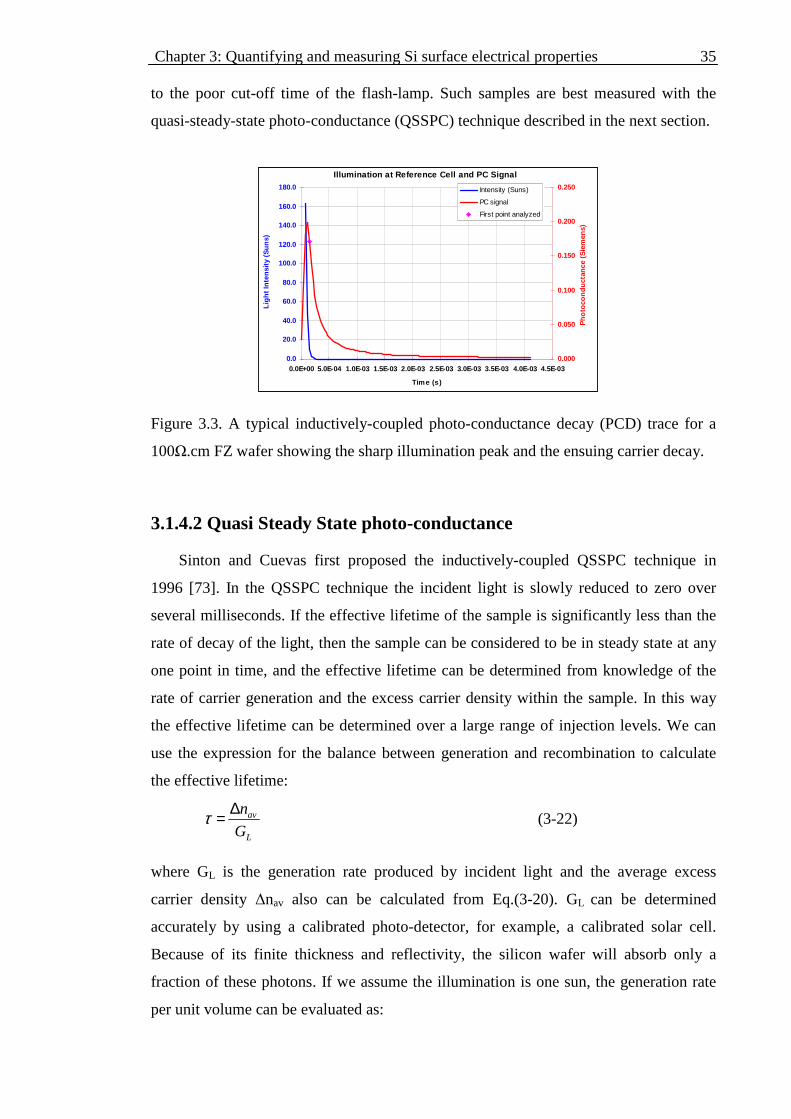
Chapter 3: Quantifying and measuring Si surface electrical properties 35
Illumination at Reference Cell and PC Signal
0.0
20.0
40.0
60.0
80.0
100.0
120.0
140.0
160.0
180.0
0.0E+00 5.0E-04 1.0E-03 1.5E-03 2.0E-03 2.5E-03 3.0E-03 3.5E-03 4.0E-03 4.5E-03
Time (s)
Lig
ht
Inte
nsi
ty (
Su
ns)
0.000
0.050
0.100
0.150
0.200
0.250
Ph
oto
con
du
ctan
ce (
Sie
men
s)
Intensity (Suns)
PC signal
First point analyzed
to the poor cut-off time of the flash-lamp. Such samples are best measured with the
quasi-steady-state photo-conductance (QSSPC) technique described in the next section.
Figure 3.3. A typical inductively-coupled photo-conductance decay (PCD) trace for a
100Ω.cm FZ wafer showing the sharp illumination peak and the ensuing carrier decay.
3.1.4.2 Quasi Steady State photo-conductance
Sinton and Cuevas first proposed the inductively-coupled QSSPC technique in
1996 [73]. In the QSSPC technique the incident light is slowly reduced to zero over
several milliseconds. If the effective lifetime of the sample is significantly less than the
rate of decay of the light, then the sample can be considered to be in steady state at any
one point in time, and the effective lifetime can be determined from knowledge of the
rate of carrier generation and the excess carrier density within the sample. In this way
the effective lifetime can be determined over a large range of injection levels. We can
use the expression for the balance between generation and recombination to calculate
the effective lifetime:
L
av
G
n∆=τ (3-22)
where GL is the generation rate produced by incident light and the average excess
carrier density ∆nav also can be calculated from Eq.(3-20). GL can be determined
accurately by using a calibrated photo-detector, for example, a calibrated solar cell.
Because of its finite thickness and reflectivity, the silicon wafer will absorb only a
fraction of these photons. If we assume the illumination is one sun, the generation rate
per unit volume can be evaluated as:

Chapter 3: Quantifying and measuring Si surface electrical properties 36
W
fNG absph
L = (3-23)
where Nph is the total photon flux incident on the surface of the wafer per unit area. fabs
is the coefficient which must be estimated or experimentally determined for each
sample to be measured.
A common feature of both techniques is that they are non-contacting, which make
them ideally suited for lifetime spectroscopic purposes, as partially finished devices that
are free of metal contacts can be investigated, even including the starting material itself.
3.2 Measurement of Si interface properties by the
Capacitance-Voltage method
Since it is well known that the characteristics of solar cells are critically dependent
on the surface condition of the semiconductor material, the properties of semiconductor
surfaces have been the subject of many investigations. A method in which the
capacitance of the semiconductor surface is studied as a function of the applied normal
electric field is provided by using a Metal-Insulator-Semiconductor (MIS) structure.
This technique is particularly easy to use in a study of oxide covered surface, since a
simple metal-oxide-semiconductor sandwich provides convenient capacitor. Soon after
the MIS structure was proposed as voltage-dependent capacitor, it was widely employed
in studies of the oxide-silicon interface [74].
3.2.1 Structure and theory of ideal Metal Insulator
Semiconductor
The MIS structure was first proposed as a voltage-variable capacitor in 1959 by
Moll [75] and by Pfann and Garrett [76]. Its characteristics were then analysed by
Frankl [77] and Lindner [78]. The MIS structure was first employed in the study of a
thermally oxidized silicon surface by Ligenza and Spitzer in 1960 [79]. A
comprehensive and in-depth treatment of the Si-SiO2 MOS structure can be found in
MOS Physics and Technology by Nicollian and Brews [80]. Figure 3.4 is the schematic
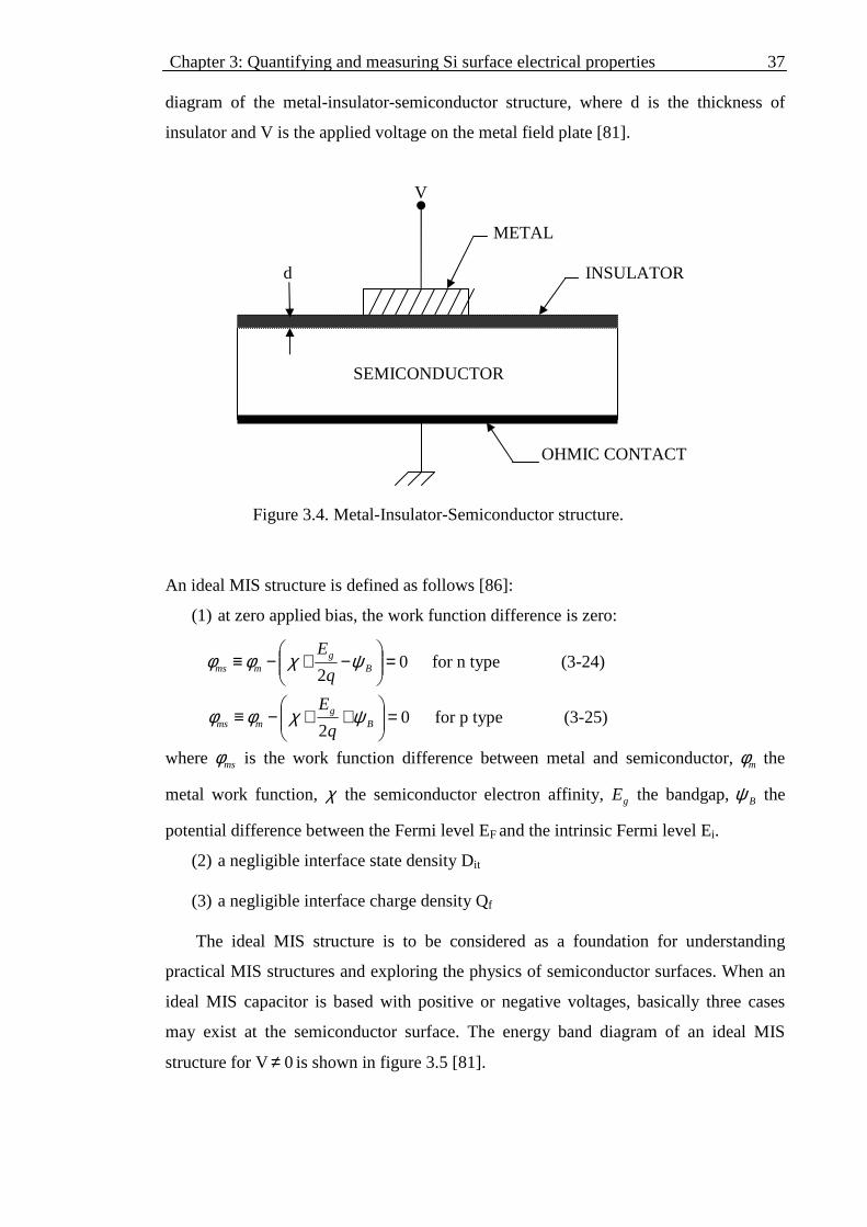
Chapter 3: Quantifying and measuring Si surface electrical properties 37
diagram of the metal-insulator-semiconductor structure, where d is the thickness of
insulator and V is the applied voltage on the metal field plate [81].
V METAL d INSULATOR SEMICONDUCTOR OHMIC CONTACT Figure 3.4. Metal-Insulator-Semiconductor structure.
An ideal MIS structure is defined as follows [86]:
(1) at zero applied bias, the work function difference is zero:
02
=
−+−≡ B
gmms q
Eψχφφ for n type (3-24)
02
=
++−≡ B
gmms q
Eψχφφ for p type (3-25)
where msφ is the work function difference between metal and semiconductor, mφ the
metal work function, χ the semiconductor electron affinity, gE the bandgap, Bψ the
potential difference between the Fermi level EF and the intrinsic Fermi level Ei.
(2) a negligible interface state density Dit (3) a negligible interface charge density Qf
The ideal MIS structure is to be considered as a foundation for understanding
practical MIS structures and exploring the physics of semiconductor surfaces. When an
ideal MIS capacitor is based with positive or negative voltages, basically three cases
may exist at the semiconductor surface. The energy band diagram of an ideal MIS
structure for V 0≠ is shown in figure 3.5 [81].
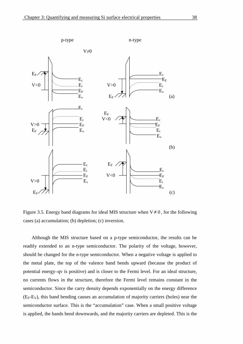
Chapter 3: Quantifying and measuring Si surface electrical properties 38
p-type n-type V≠0 EF Ec Ec EF V<0 Ei V>0 Ei EF Ev Ev EF (a) Ec EF Ei V<0 Ec V>0 EF EF EF Ev Ei Ev (b) Ec EF Ei Ec EF V<0 EF V>0 Ev Ei Ev EF (c)
Figure 3.5. Energy band diagrams for ideal MIS structure when V 0≠ , for the following
cases (a) accumulation; (b) depletion; (c) inversion.
Although the MIS structure based on a p-type semiconductor, the results can be
readily extended to an n-type semiconductor. The polarity of the voltage, however,
should be changed for the n-type semiconductor. When a negative voltage is applied to
the metal plate, the top of the valence band bends upward (because the product of
potential energy–qv is positive) and is closer to the Fermi level. For an ideal structure,
no currents flows in the structure, therefore the Fermi level remains constant in the
semiconductor. Since the carry density depends exponentially on the energy difference
(EF-EV), this band bending causes an accumulation of majority carriers (holes) near the
semiconductor surface. This is the “accumulation” case. When a small positive voltage
is applied, the bands bend downwards, and the majority carriers are depleted. This is the

Chapter 3: Quantifying and measuring Si surface electrical properties 39
“depletion” case. When a large positive voltage is applied, the bands bend even more
downward so that the intrinsic level Ei at the surface cross over the Fermi level Ef. At
this point the number of electrons (minority carriers) at the surface is larger than that of
the holes, the surface is thus inverted, and this is the inversion case [81]. Note that if the
C-V curve is made from the accumulation side, non-equilibrium depletion
characteristics prevent the measurement of the interface state. Thus C-V curves must be
made from inversion to accumulation. For this plot direction the sweep rate has not been
found to affect the interface states measurement [82].
3.2.2 Calculation of the overall electrical characteristics of
silicon surfaces
The essence of the MIS technique lies in a comparison between an idealised theory
and experimental observations; conclusions regarding the nature of the interface are
based upon interpretation of the deviations between the two. Many detailed properties
of the oxide-silicon interface, such as the surface state density, the fixed surface charge
density, and the dependence between the surface band bending and the applied gate
voltage and so on, can be obtained from C-V technique.
Terman [83] developed and used the high frequency method for determining
interface trap capacitance. In the high frequency capacitance method, capacitance is
measured as a function of gate bias with frequency fixed at a high enough value so that
interface traps do not respond and contribute no capacitance to the high frequency C-V
curve. However, these interface traps will cause stretch-out or distortion on the high
frequency curve along the gate bias axis compared to an ideal C-V curve. On the other
hand, oxide fixed charge and work function difference will produce a parallel shift of
the C-V curve along the gate bias axis compared to an ideal C-V curve. At high
frequency, capacitance is given by:
si CC
C11 += (3-26)
where iC is insulator capacitance, sC the semiconductor capacitance.
Berglund [84] developed and was first to use the low frequency C-V method.
Again, a C-V curve is measured at a constant frequency, but now at a frequency so low
that interface trap response is immediate. Because interface traps immediately respond
to the ac gate voltage, they will contribute an additional capacitance to the measured
low frequency C-V curve. In addition, interface traps follow changes in gate bias so that

Chapter 3: Quantifying and measuring Si surface electrical properties 40
-6 -4 -2 0 20.0
0.2
0.4
0.6
0.8
1.0
C/C
i
Applied voltage (V)
HFCVQSCV
passivated sample
(a)
-6 -4 -2 0 20.0
0.2
0.4
0.6
0.8
1.0
C/C
i
Applied voltage(V)
HFQS
depassivated sample
(b)
the measured low frequency C-V curve will stretched out along the gate bias like the
high frequency C-V curve. At low frequency, capacitance is given by:
itsi CCC
C+
+= 11 (3-27)
where itC is the interface trap capacitance.
Castagne and Vapaille [85] were the first to combine high and low frequency C-V
curves to obtain a measured semiconductor capacitance. In our C-V measurements, the
quasi-static C-V technique was used. This method is based on the proportionality that
exists between MOS capacitance and the charging current in the structure when it is
subjected a linear voltage ramp. As a result of this proportionality, a low frequency
thermal-equilibrium capacitance-voltage curve can be obtained. The quasi-static and
high-frequency curves are then used to extract the interface-states density distribution in
the band gap.
C-V curves at high frequency and under quasi static conditions for Si-SiO2
structures are shown in figure 3.6 (a) passivated sample and (b) depassivated sample. A
(100), p type, 1-10Ω.cm, single side polished Si wafer was used. A 50nm thick oxide
layer was thermally grown on Si followed by an in-situ anneal in N2 at the oxidation
temperature and FGA at 400oC for 30 minutes for passivated sample and followed by a
RTA 700oC for 3 minutes for depassivated sample.
Figure 3.6. High frequency and Quasi static CV curves for p-type Si-SiO2 structures (a)
passivated (b) depassivated.
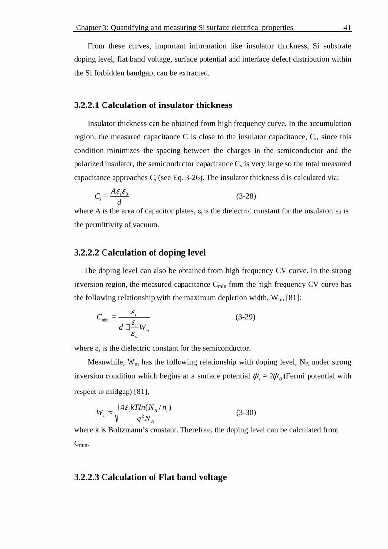
Chapter 3: Quantifying and measuring Si surface electrical properties 41
From these curves, important information like insulator thickness, Si substrate
doping level, flat band voltage, surface potential and interface defect distribution within
the Si forbidden bandgap, can be extracted.
3.2.2.1 Calculation of insulator thickness
Insulator thickness can be obtained from high frequency curve. In the accumulation
region, the measured capacitance C is close to the insulator capacitance, Ci, since this
condition minimizes the spacing between the charges in the semiconductor and the
polarized insulator, the semiconductor capacitance Cs is very large so the total measured
capacitance approaches Ci (see Eq. 3-26). The insulator thickness d is calculated via:
d
AC i
i0εε= (3-28)
where A is the area of capacitor plates, εi is the dielectric constant for the insulator, ε0 is
the permittivity of vacuum.
3.2.2.2 Calculation of doping level
The doping level can also be obtained from high frequency CV curve. In the strong
inversion region, the measured capacitance Cmin from the high frequency CV curve has
the following relationship with the maximum depletion width, Wm, [81]:
ms
i
i
WdC
εεε
+=min (3-29)
where εs is the dielectric constant for the semiconductor.
Meanwhile, Wm has the following relationship with doping level, NA under strong
inversion condition which begins at a surface potential Bs ψψ 2≈ (Fermi potential with
respect to midgap) [81],
A
iAsm Nq
nNkTInW
2
)/(4ε≈ (3-30)
where k is Boltzmann’s constant. Therefore, the doping level can be calculated from
Cmin.
3.2.2.3 Calculation of Flat band voltage

Chapter 3: Quantifying and measuring Si surface electrical properties 42
Referring to MIS devices, flat band voltage is the voltage at which the surface
potential is zero, therefore, no voltage drop across the semiconductor; in band diagram
the energy bands of the semiconductor are horizontal (flat). The flat band voltage of real
MOS structures is further affected by the presence of charge in the oxide or at the oxide-
semiconductor interface and can be calculated from the high frequency C-V curve.
At flat band conditions, the semiconductor capacitance is given by [81]:
D
ss L
Cε
= (3-31)
where LD is the Debye length which is a measure of the distance over which a charge
imbalance is neutralized by majority carriers under steady-state or equilibrium
conditions, and is given by:
A
sD Nq
kTL
2
ε= (3-32)
The flat band capacitance can be calculated from a combination of equations (3-26),
(3-31) and (3-32) and obtained from corresponding capacitance value in CV curve.
3.2.2.4 Calculation of fixed oxide charge density
Oxide charges Qo include the oxide fixed charge Qf, the oxide trapped charge Qot,
and the mobile ionic charge Qm.
Qo≡Qf +Qot+Qm (3-33) The fixed oxide charge Qf has the following properties: it is fixed and cannot be
charged or discharged over a wide variation of sψ ; it is located in the oxide layer less
than 25Å from the Si-SiO2 interface; its density is not greatly affected by the thickness
or by the type or concentration of impurities in the silicon; it is generally positive and
depends on oxidation and annealing conditions, and on silicon orientation. It has been
suggested that the silicon dangling bonds or the loss of an electron from excess oxygen
centres near the Si-SiO2 interface is the origin of fixed oxide charge. In electrical
measurements, Qf can be regarded as a charge sheet located at the Si-SiO2 interface [86,
87].
For a practical CV experiment, the value of work function difference msΦ is not
zero and the oxide charge exist, so if we assume negligible interface traps, the
experimental Capacitance-voltage curve will be shifted from the ideal curve by an
amount

Chapter 3: Quantifying and measuring Si surface electrical properties 43
i
otmfms
i
omsFB C
QQQ
C
QV
++−Φ=−Φ= (3-34)
If mobile ions and oxide trapped charges are negligible, Eq. (3-34) reduces to
i
f
msFB C
QV −Φ= (3-35)
For a certain MIS structure, msΦ is a constant, therefore, the fixed oxide charge density
can be calculated from FBV and iC .
According to the analysis above, fixed oxide charge density can not be determined
unambiguously in the presence of moderate densities of interface trapped charge, it is
only measured after a low-temperature (minus 450oC) hydrogen treatment to minimise
trap density [88].
3.2.2.5 Calculation of interface defect density and surface potential
By comparing the Metal Insulator Semiconductor (MIS) capacitance at high and low
frequency, Castagne [85] pointed out the areal interface defect density, Dit, has the
following relationship with capacitance
)(1
)(hfi
hfi
lfi
lfigit CC
CC
CC
CC
qAVD
−−
−= (3-36)
where A is the surface area, lfC is the low frequency capacitance and hfC is the high
frequency capacitance. The dependence between the gate voltage gV and surface
potential sψ is determined by Berglund’s [84] formula
( ) ( )( ) gVgVfb iglfgs dVCVCV ∫ −= /1ψ (3-37)
Combining equation (3-28) to (3-37), a computer program written in Matlab was
used to analyse the Dit distribution within the Si forbidden bandgap. It should be noted
that because equation (3-36) takes the difference between the quasi static and high
frequency CV curves to calculate Dit, it is not valid for gate biases at accumulation
where the capacitance is too small or in or near inversion where minority carriers do not
follow the high frequency gate voltage. Such a determination is valid only in a limited
interval of the forbidden gap. In practice, the range extends flatband condition to the
onset of strong inversion; this means from Ei-∆ to ~Ei+∆/2, where Ei-∆=Efb (i.e. flatband,
this is for p type). In principle, the extraction of Dit
from the measurements is most

Chapter 3: Quantifying and measuring Si surface electrical properties 44
0.2 0.4 0.6 0.81E9
1E10
1E11
1E12
Dit(
eV-1cm
-2)
Bandgap energy (eV)
accurate for energies spanning the range from flatband conditions to the onset of strong
inversion at the surface (~Ev+0.26eV to Ev+0.86eV). It should be noted that,
considering the parameters (including metal area, insulator thickness and insulator
permittivity) used in the analysing software, there is a measurement error for Dit to
about ±10%.
Figure 3.7 shows the Dit distribution for a (100), p-type, 1-10Ω.cm, single side
polished, oxidised and passivated Si wafer.
Figure 3.7. Dit distribution in the Si forbidden bandgap for p-type, passivated sample.
3.3 Measurement of paramagnetic interface defects by
Electron Paramagnetic Resonance
3.3.1 Paramagnetic point defects at the Si-SiO2 interface
Electron paramagnetic resonance is perhaps the only spectroscopic tool which
responds exclusively to detect atomic states in Si-SiO2 system. Of all the EPR signals
reported in Si-SiO2 system, Pb appears to be most pertinent to the inherent defect
structure of the interface, whereas Pc is due to iron contamination, and Pa resembles the
signal from donor or conduction electrons [88, 89]. In the last decades, the very
important dangling orbital or paramagnetic centres have been the object of extensive

Chapter 3: Quantifying and measuring Si surface electrical properties 45
research in all forms of silica, crystalline [90], vitreous [91], and thermal thin film [92,
93]. Most of the paramagnetic defects which have been observed in thermal silica are
shown in figure 3.8 [2].
Figure 3.8. Paramagnetic point defects observed in Si-SiO2 structures by electron
paramagnetic resonance [2].
Actually, the early results from EPR were rather lightly dismissed by the MIS
device community, due to unconvincing interpretations [88, 94]. However, they were
later superseded by solid and correct identifications [89]. These included the critical Pb
centre, deduced to be an ·Si≡Si3 structure occurring precisely at the Si-SiO2 interface.
The Pb centre is by far the most important defect identified at the interface, and its
observation and correct assignment have touched off numerous research activities on
the interface.
3.3.2 EPR operation and calculation of Pb-type defect density
EPR measurements of the Si interface defect (Pb) centres were undertaken using a
Bruker 300E spectrometer operating at X Band (9.44 GHz), fitted with an Oxford ES-9
liquid helium cryostat with temperature control via an Oxford ITC-4 controller.
Measurements were done using a modulation frequency of 100kHz, modulation
amplitude (MA) of 1.011G and a microwave power of 20µW at a temperature of around

Chapter 3: Quantifying and measuring Si surface electrical properties 46
2200 2400 2600 2800 3000 3200 3400 3600 3800-100000
-80000
-60000
-40000
-20000
0
20000
40000
EP
R s
igna
l(arb
.uni
t)
Magnetic field (B)
signal from Cu(NO3)2 solution
6.5K. The low temperature is realized by immersing the tubes containing the samples
into liquid helium. The defect spin at the Si interface saturates when a high microwave
power is applied. 20µW was observed to be non-saturating. Samples were placed in 3
mm ID quartz EPR tubes, which were flushed with pure argon to remove oxygen. The
sample tubes were sealed with rubber septa and the sample end frozen to 77K. The
angle between the sample surface and the magnetic field is less than 3o.
A Cu(NO3)2 solution of known molarity is used for instrument calibration. The
spectrum shown in figure 3.9 was obtained at a temperature of around 6.5K, MA of
10.115G and microwave power of 0.1mW. The conditions used for obtaining the Cu2+
spin signal are similar to those used for measuring Pb centres in order to allow a direct
and accurate comparison between the two signals.
Figure 3.9. EPR spectrum from Cu(NO3)2 solution. The total spin number is calculated from the following equation:
MWPGMS
pts
SWTDI
KSNAcan
G
pin ×××
××=
#
#
2
(3-38)
where K is a constant determined by calibration with the Cu(NO3)2 solution, DI is the
absolute value of the signal obtained by double integrating the spin signal, SWG is the
field sweep width, #pts is the resolution, #Scan is the number of scan, GN is the receiver
gain level, MWP (W) is the microwave power in the unit of watt, and T (K) is the
Chapter 3: Quantifying and measuring Si surface electrical properties 47
temperature in Kelvin. From the solution signal, K is determined to be 9.68×10¹¹. All
spin density calculations in this work are obtained with this K value.
The bP defects density,[ ]bP , can be obtained from the following equation:
[ ]bPA
S pin= (3-39)
where A is the sample’s area, in this work the EPR sample’s size is 25mm× 2.5mm.
EPR measurements of Pb-type defects on the (111) rather than the (100) Si-SiO2
interface are preferred two reasons [37]. First, the signal-to-noise ratio is greater in the
case of (111) interface because of its greater interface state density. Second, the (111)
Si-SiO2 interface has only one type of paramagnetic defect, namely the Pb centre,
whereas two distinct paramagnetic defects, namely, Pb1 and Pb0 centres, are associated
with (100) Si-SiO2 interface. These two defects give rise to only two partially
overlapping resonances providing the applied magnetic field is perpendicular to the
(100) interface [95]. This complications make it very difficult to measure the intensity
of the individual defect spectra associated with the (100) interface. Actually, for
standard oxidation temperatures (800-950°C), areal densities of physical defect sites
(including both ESR active and inactivated ones) of [Pb] ~5×1012cm-2 and [Pb0], [Pb1]
~1×1012cm-2 are naturally incorporated [23]. Thus, the EPR experiments in this thesis
are limited to the (111) interface.
3.4 Summary
This chapter briefly describes the main measurement techniques and the theory
behind them used in this dissertation for Si electronic properties. A combination of
lifetime and Capacitance-Voltage is mainly used to analyse the properties of Si-SiO2
interface. The fundamental recombination mechanisms in silicon have been discussed.
Photo-conductance based methods are used for determining the effective lifetime and
emitter saturation current density, which are parameters widely used in the photovoltaic
community for developing, optimizing and maintain process control for surface
passivation.
C-V technique, in which the capacitance of the semiconductor surface is studied as
a function of the applied normal electric field, is particularly easy to use in a study of
MOS stack as it provides a convenient capacitor. C-V technique determines the

Chapter 3: Quantifying and measuring Si surface electrical properties 48
effective interface charge density and the density of interface states within the forbidden
bandgap of silicon, which represent two critical parameters related to the electrical
properties of the Si-SiO2 interface.
Electronic Paramagnetic Resonance measurements allow the determination of the
density of a specific interface defect, conclusively identified as three-fold coordinated
interfacial silicon, which is EPR active when neutral and is known to be a detrimental
electrically active interface defects. The thermochemical characters of this kind defect
appear dominated by interaction with hydrogen.

Chapter 4: Experimental 49
CHAPTER 4
Experimental
Collected in this chapter are descriptions of three main processing equipments used
in this thesis and general and standard lifetime and C-V samples processing conditions.
The three main equipments are PECVD reactor, Rapid thermal annealing (RTA) reactor
and Temperature and injection dependent lifetime spectroscopy (TIDLS) system.
Details specific to experiments are described in the relevant chapters.
4.1 Hydrogenation Systems
For the routine injection of atomic hydrogen controlled methods are required. There
are two common methods for achieving this objective: exposure to a low power density
H2 plasma; or implantation of very low energy H+ ions from a broad beam source. In
this thesis, a remote PECVD system was used to produce hydrogen plasma.
Chapter 4: Experimental 50
4.2 Hydrogenation Plasma Exposure
Usually, the hydrogenation systems used by most researchers are relatively simple
and generally consist of a quartz tube through which molecular hydrogen is pumped at a
reduced pressure. The plasma is excited by capacitively or inductively coupling low-
frequency (~30kHz) or radio-frequency (13.56MHz) power via a high frequency
oscillator or a copper coil encircling the quartz tube [96]. It is, of course, possible to use
commercially available plasma-assisted deposition reactors in which the electrodes are
inside the chamber. Hydrogen is introduced at reduced pressure into the system and
ionized by a dc voltage.
Normally, the plasma is a combination of positive and negative ions, molecules,
neutral atoms and free radicals, which is neutral overall [97]. The hydrogen gas also
shows emission from its vibrational levels, causing to the familiar light purple colour of
the discharge. The electron energy in these plasmas is typically 1-10eV with an electron
density of 109-1012cm-3 [98]. The sample therefore is subjected to ion and electron
bombardment and a high level of UV and visible light exposure unless optical baffles
are used, and the plasma is contained upstream from the sample. Several experiments
have demonstrated the incorporation of atomic hydrogen into Si [99, 100], using a
simple two-electrode electrochemical cell, by which atomic hydrogen is introduced to
crystalline silicon to passivate deep bulk defects. Under these circumstances, there is no
bombardment but defect passivation results similar to plasma hydrogenation are
obtained in this method of hydrogen insertion. Pure bombardment-related effects can be
examined using He plasmas in place of active hydrogen. Under high-power density
conditions, or when using very pure samples (doping density<1014cm-3), damage related
levels can be observed in the near-surface region after direct exposure to a hydrogen
plasma [101].
Whatever method of hydrogen insertion is used, one needs to be aware of the
possible pitfalls of that particular technique. For example, high leakage current in
hydrogenated diode structures for C-V measurements is an indication of the presence of
plasma-induced surface damage or a contaminating layer deposited during the exposure.
In our hydrogen plasma exposure experiments, the samples were exposed to atomic
H in a remote plasma system by using a commercially available plasma-assisted
deposition reactor, Roth&Rau AK400 PECVD system. Figure 4.1 shows schematic of
PECVD reactor, dashed line means the RF power generator can not be seen from this
section view. In this plasma system, in addition to the two quartz glass tubes the plasma
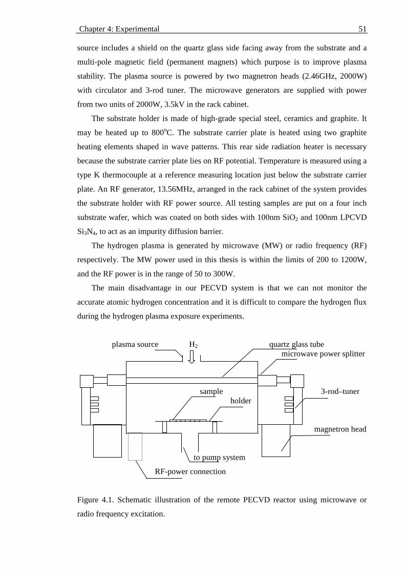
Chapter 4: Experimental 51
source includes a shield on the quartz glass side facing away from the substrate and a
multi-pole magnetic field (permanent magnets) which purpose is to improve plasma
stability. The plasma source is powered by two magnetron heads (2.46GHz, 2000W)
with circulator and 3-rod tuner. The microwave generators are supplied with power
from two units of 2000W, 3.5kV in the rack cabinet.
The substrate holder is made of high-grade special steel, ceramics and graphite. It
may be heated up to 800oC. The substrate carrier plate is heated using two graphite
heating elements shaped in wave patterns. This rear side radiation heater is necessary
because the substrate carrier plate lies on RF potential. Temperature is measured using a
type K thermocouple at a reference measuring location just below the substrate carrier
plate. An RF generator, 13.56MHz, arranged in the rack cabinet of the system provides
the substrate holder with RF power source. All testing samples are put on a four inch
substrate wafer, which was coated on both sides with 100nm SiO2 and 100nm LPCVD
Si3N4, to act as an impurity diffusion barrier.
The hydrogen plasma is generated by microwave (MW) or radio frequency (RF)
respectively. The MW power used in this thesis is within the limits of 200 to 1200W,
and the RF power is in the range of 50 to 300W.
The main disadvantage in our PECVD system is that we can not monitor the
accurate atomic hydrogen concentration and it is difficult to compare the hydrogen flux
during the hydrogen plasma exposure experiments.
plasma source H2 quartz glass tube microwave power splitter sample 3-rod–tuner holder magnetron head
to pump system
RF-power connection
Figure 4.1. Schematic illustration of the remote PECVD reactor using microwave or
radio frequency excitation.

Chapter 4: Experimental 52
4.3 Rapid thermal annealing
Rapid thermal anneals (RTA) are frequently used in photovoltaic research and
manufacturing [102-105]. They provide a means to fire metal contacts, to densify
dielectric films, to remove hydrogen from interfaces, and to drive hydrogen from silicon
nitride films into underlying silicon.
In our experiments, RTA is mainly utilised to accomplish the dehydrogenation of Si-
SiO2 stacks as well as the post-hydrogen plasma exposure thermal annealing. De-
hydrogenation can be achieved by RTA under conditions of 700oC, 3 minutes in N2
ambient. In this case, the dissociation reaction of pre-existing PbH centres will dominate
the Si-SiO2 interface and meanwhile little additional Pb defects will be generated. The
post-hydrogen plasma exposure thermal annealing can be achieved by RTA under
conditions of below 400oC, 3 minutes in N2 ambient. Because the Si-SiO2 interface can
be affected by even small amounts of moisture in the atmosphere, making results
difficult to interpret, therefore a dry (moisture and H free) atmosphere was needed to
ensure a purely thermal treatment. The RTA had been previously tested and found to
provide this [106] (when N2 is used) while other furnaces do not. However, when
applying RTA treatment, there are some disadvantages, such as the illumination effect
during RTA; the difference between the actual temperature and target temperature due
to the contact problem between the thermocouple and the test sample; and the
possibility of sample contamination. These limitations sometimes lead to inconsistent
results following RTA treatments.
In this thesis, the RTA annealing treatments were carried out in a Unitemp 1100
oven. High-intensity lamps shown in figure 4.2 are used to rapidly heat the wafer to the
desired annealing temperature in a very short time. Extremely rapid temperature ramp-
up and ramp-down rates are achieved. Samples, which received atomic hydrogen
plasma exposure, were loaded into the RCA cleaned chamber. A thermocouple was
attached to the back of one testing samples to monitor its temperature during the run,
which was assumed equal to the testing samples temperature. A typical RTA at 400oC
was carried out as follows. After loading samples, the chamber was purged in N2 for 1
minute before the temperature was ramped for ~40 seconds to 400°C with a gradually
decreased rate. The samples were maintained for 3 minutes in N2 and then cooled
rapidly by turning off the IR lamps and flushing the chamber with a high flow of N2. It
should be noted that illumination under the conditions used in this thesis does not

Chapter 4: Experimental 53
0 100 200 300 400 500 600
0
50
100
150
200
250
300
350
400
450
Tem
pera
ture
(o C
)
Time (s)
400oC RTA 3min
produce any defects. Figure 4.3 plots the temperature profile of standard RTA annealing
program.
Figure 4.2. Schematic illustration of the rapid thermal annealing (RTA) apparatus.
Figure 4.3. Temperature profile of 400oC RTA annealing.
High-intensity lamps in light pipes
Thermal energy
wafer
Thermal couple
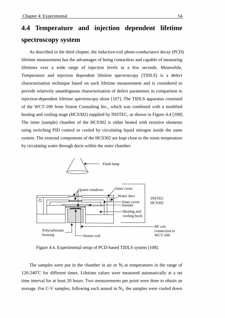
Chapter 4: Experimental 54
Flash lamp
Polycarbonate housing Sensor coil
Quartz windows Outer cover
Water duct
Inner cover Sample
Heating and cooling bock
INSTEC HCS302
RF coil connection to WCT-100
4.4 Temperature and injection dependent lifetime
spectroscopy system
As described in the third chapter, the inductive-coil photo-conductance decay (PCD)
lifetime measurement has the advantages of being contactless and capable of measuring
lifetimes over a wide range of injection levels in a few seconds. Meanwhile,
Temperature and injection dependent lifetime spectroscopy (TIDLS) is a defect
characterisation technique based on such lifetime measurement and is considered to
provide relatively unambiguous characterisation of defect parameters in comparison to
injection-dependent lifetime spectroscopy alone [107]. The TIDLS apparatus consisted
of the WCT-100 from Sinton Consulting Inc., which was combined with a modified
heating and cooling stage (HCS302) supplied by INSTEC, as shown in Figure 4.4 [108].
The inner (sample) chamber of the HCS302 is either heated with resistive elements
using switching PID control or cooled by circulating liquid nitrogen inside the same
system. The external components of the HCS302 are kept close to the room temperature
by circulating water through ducts within the outer chamber.
Figure 4.4. Experimental setup of PCD-based TIDLS system [108].
The samples were put in the chamber in air or N2 at temperatures in the range of
120-240oC for different times. Lifetime values were measured automatically at a set
time interval for at least 20 hours. Two measurements per point were done to obtain an
average. For C-V samples, following each anneal in N2, the samples were cooled down

Chapter 4: Experimental 55
to room temperature and C-V measurements were carried out on the same dot. The
sample were then returned to the anneal chamber for additional processing, and then
retested.
4.5 General sample processing
Most samples used for lifetime measurements were FZ, p-type, 100-1000Ω.cm,
(100), 550µm thick silicon wafers. Samples for C-V measurements were CZ, p-type, 1-
10Ω.cm, (100), single side polished silicon wafers. Treatments applied to these samples
are listed in table 4.1 and table 4.2.
Table 4.1 Experimental processes for lifetime sample preparation
Step Description Chemical Details
1 Saw damage
etch
Tetramethyl
ammonium hydroxide
(TMAH) solution
Remove saw damage from Si surface
and edges by etching in TMAH
solution at 85oC for 20 minutes
2 Saw damage
etch
HF:HNO3 solution Remove saw damage from Si surface
and edges by etching in HF:HNO3
solution for 2 minutes
3 Cleaving (100) wafers were cleaved into
quarters and labelled
4 RCA clean 1 5:1:1 H2O:NH4OH:
H2O2 solution
For 10 minutes in warm solution
(~80oC)
5 RCA clean 2 5:1:1 H2O: HCl: H2O2
solution
For 10 minutes in warm solution
(~80oC)
6 HF dip Clean 10% HF
solution
Until hydrophobic to remove native
oxide
7 Light
phosphorous
diffusion
POCl3 and O2 In TCA cleaned furnace at 764oC for
20 minutes followed by an in situ
drive in process in N2 for 10 minutes
on selected samples.
8 HF dip Clean 10% HF
solution
Until hydrophobic to remove
phosphorous glass
9 Oxidation O2 In TCA cleaned furnace at 1000oC to

Chapter 4: Experimental 56
grow ~50nm oxide layers, followed
by an in situ anneal in N2 for 30
minutes on selected samples.
10 Forming gas
anneal (FGA)
Forming gas (5% H2
in 95% Ar)
FGA at 400oC for 30 minutes to
hydrogenate the Si/SiO2 interface
Table 4.2 Experimental processes for CV sample preparation
Step Description Chemical Details
1 Saw damage etch HF:HNO3 solution Remove saw damage from Si
surface and edges by etching in
HF:HNO3 solution for 2 minutes
2 Cleaving (100) wafers were cleaved into
quarters and labelled
3 RCA clean 1 5:1:1 H2O:NH4OH:
H2O2 solution
For 10 minutes in warm solution
(~80oC)
4 RCA clean 2 5:1:1 H2O: HCl:
H2O2 solution
For 10 minutes in warm solution
(~80oC)
5 HF dip Clean 10% HF
solution
Until hydrophobic to remove
native oxide
6 Oxidation O2 In TCA cleaned tube at 1000oC
to grow ~50nm oxide layers,
followed by an in situ anneal in
N2 for 30 minutes on selected
samples.
7 Forming gas
anneal (FGA)
Forming gas (5% H2
in 95% Ar)
All samples receive FGA at
400oC for 30 minutes to
hydrogenate the Si-SiO2
interface
8 HF fume HF bottle
concentration
solution
One side of oxide was removed
by HF fume
9 Al deposition Al At high vacuum (<3×10⁻⁶ torr),

Chapter 4: Experimental 57
~80nm thick Al was deposited
on oxide layer through a shadow
mask with area of 4.7×10⁻³ cm2
10 Ohmic contact Ga-In Ohmic contact by Ga-In paste
on oxide free Si side
4.6 Summary
Three major experimental equipments used in this thesis as well as the general and
standard lifetime and C-V sample processing conditions are described in this chapter.
The hydrogen plasma exposure experiments were carried out by using a
commercially available plasma-assisted PECVD deposition reactor. The plasma source
is powered by either microwave or radio frequency. The main disadvantage in our
PECVD system is that it is difficult to monitor the accurate atomic hydrogen
concentration.
Rapid thermal annealing has replaced the tube furnace in many applications to
perform solar cell processing steps for dehydrogenation or defect annealing. Although a
precise control of thermal profile can be achieved during RTA processing, the impact of
illumination and/or contact problem between the thermocouple and testing sample
should be considered sometimes.
Temperature and injection dependent lifetime spectroscopy (TIDLS) is a relatively
simple defect characterisation technique to provide relatively unambiguous
characterisation of defect parameters in comparison to injection-dependent lifetime
spectroscopy alone, which can be applied to a large temperature range. Because this
technique is based on the inductive coil photo-conductance lifetime measurement, the
disadvantage of being affected by such as depletion-region modulation for diffused
samples is always unavoidable.

Chapter 4: Experimental 58

Chapter 5: Passivation effect of wet oxidation, and with oxide/LPCVD nitride stacks on the Si-SiO2 interface
59
CHAPTER 5
Passivation effect of wet oxidation, and
with oxide/LPCVD nitride stacks on the
Si-SiO2 interface
In this chapter the passivation achieved with relatively low temperature, thin thermal
oxides which are grown in the temperature range 750-900oC in wet oxidation (with
steam) conditions, and with oxide/LPCVD nitride stacks is investigated. Dry and wet
oxidations at different temperatures are compared and the surface recombination
velocities of (100), (111) and textured Si surfaces are studied. The thermal stability of
thin oxide and oxide/LPCVD nitride stacks are also studied. The influence of
phosphorous diffusion on Si surface passivation is discussed.

Chapter 5: Passivation effect of wet oxidation, and with oxide/LPCVD nitride stacks on the Si-SiO2 interface
60
5.1 Introduction
High oxidation temperatures (1100-1200oC) achieve the lowest density of interface
states within the forbidden gap of silicon at the Si-SiO2 interface. This translates to
lower recombination losses at the silicon surfaces. Very thin SiO2 (-100Å) layers are
routinely used in high-efficiency silicon solar cells, MOSFET, and advanced bipolar
devices to reduce surface recombination or to provide high-quality insulating layers.
Generally, the thin oxide is formed by high temperature (850-1050oC) oxidation
because low-temperature processing generally produces low-quality oxides with high
recombination velocity at the Si-SiO2 interface [109].
However, high process temperatures are generally undesirable for solar cell
fabrication for a number of reasons, including a higher risk of contamination of the
wafer bulk, and the fact that the effective lifetime of multi-crystalline silicon in
particular often degrades following high temperature treatments [110]. In addition,
higher temperature processing requires more energy to run, and thus resulting in higher
manufacturing cost. Therefore, high temperature dry oxidation is not readily applicable
as an industrial process and surface passivation processes at lower temperatures have
become very important in silicon solar cell fabrication, particularly for thin silicon
wafers. Among a large number of developed passivation layers for crystalline silicon
surfaces, low temperature oxides are desirable for greater flexibility in the process
sequence and preservation of minority carrier lifetime in high performance silicon
devices [111]. Ideally the oxide should be grown rapidly, at low temperatures and low
cost. It should also be thin enough not to increase substantially the reflectance of the
surface. There are several other possible methods for oxide preparation in addition to
thermally grown SiO2, such as low temperature PECVD oxides which generally have
Dit values that are slightly higher but nearly comparable to thermally grown oxides at
high temperatures [110], and intrinsic hydrogenated amorphous silicon oxide (a-SiOX:H)
prepared by very high frequency plasma-enhanced chemical vapour deposition(VHF-
PECVD) at a very low substrate temperature (170oC) with maximum effective lifetime
of 400µs measured for 1-10Ω.cm, 380µm, p-type silicon wafer [110].
Wet oxidations using water vapour can give about the same Dit values as oxidations
performed with dry oxygen, but result in higher positive oxide charges [80]. This offers
interesting possibilities with regard to the field-effect passivation method.

Chapter 5: Passivation effect of wet oxidation, and with oxide/LPCVD nitride stacks on the Si-SiO2 interface
61
The work in this chapter is aimed at thin oxide and thin oxide/LPCVD nitride stacks,
with the thin oxide having the purpose of providing good surface passivation. Given
that low process temperatures are generally desirable, it is of interest to determine how
oxide passivation quality varies with oxidation temperature. Wet oxidations at
temperatures in the range 750-900oC were carried out, and the J0e values obtained from
these oxides compared with the J0e value from a high temperature, dry oxide. In general,
there is a clear trend of increasing surface recombination with decreasing oxidation
temperature, with a particularly significant increase between 800 and 850oC. However,
very good surface passivation was achieved when a low temperature (750oC) oxidation
was followed by a phosphorous diffusion into the oxide.
5.2 Effect of low temperature oxides on the passivation
of Si-SiO2 interface In this section, work is focused on the properties of low temperature thermally
grown oxides, and in particular on the effect of oxidation temperature.
5.2.1 Experimental details
A detailed description of lifetime and C-V measurements is given in previous
chapters. Lifetime samples received a standard phosphorous diffusion and oxidation.
The oxide was then stripped by 10% HF solution and another oxide with different
processing conditions was grown. This was done to ensure nearly identical phosphorous
diffusion profiles for samples with different oxides, since the oxidation temperature for
the second oxidation was lower than that of the first oxidation. The oxidation conditions
were chosen to give approximately the same oxide thickness in each case of ~30nm.
The actual oxide thicknesses were measured using a Filmetrics F20-UV film
measurement system. Table 5.1 summarizes the second oxidation conditions and the
oxide thicknesses.
Following the second oxidation, the samples received a number of additional
treatments for different experiments
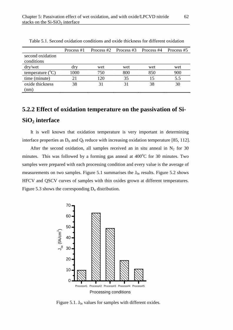
Chapter 5: Passivation effect of wet oxidation, and with oxide/LPCVD nitride stacks on the Si-SiO2 interface
62
Process#1 Process#2 Process#3 Process#4 Process#5
0
10
20
30
40
50
60
70
J 0e (
fA/c
m2 )
Processing conditions
Table 5.1. Second oxidation conditions and oxide thickness for different oxidation
5.2.2 Effect of oxidation temperature on the passivation of Si-
SiO2 interface
It is well known that oxidation temperature is very important in determining
interface properties as Dit and Qf reduce with increasing oxidation temperature [85, 112].
After the second oxidation, all samples received an in situ anneal in N2 for 30
minutes. This was followed by a forming gas anneal at 400oC for 30 minutes. Two
samples were prepared with each processing condition and every value is the average of
measurements on two samples. Figure 5.1 summarises the J0e results. Figure 5.2 shows
HFCV and QSCV curves of samples with thin oxides grown at different temperatures.
Figure 5.3 shows the corresponding Dit distribution.
Figure 5.1. J0e values for samples with different oxides.
Process #1 Process #2 Process #3 Process #4 Process #5 second oxidation conditions
dry/wet dry wet wet wet wet temperature (oC) 1000 750 800 850 900 time (minute) 21 120 35 15 5.5 oxide thickness (nm)
38 31 31 38 30

Chapter 5: Passivation effect of wet oxidation, and with oxide/LPCVD nitride stacks on the Si-SiO2 interface
63
-8 -6 -4 -2 0 20.0
0.2
0.4
0.6
0.8
1.0
C/C
i
Applied voltage (V)
750oC wet QSCV 750oC wet HFCV(a)
-8 -6 -4 -2 0 20.0
0.2
0.4
0.6
0.8
1.0
C/C
i
Applied voltage (V)
800oC wet QSCV 800oC wet HFCV(b)
-8 -6 -4 -2 0 20.0
0.2
0.4
0.6
0.8
1.0
C/C
i
Applied voltage (V)
850oC wet QSCV
850oC wet HFCV(c)
-8 -6 -4 -2 0 20.0
0.2
0.4
0.6
0.8
1.0
C/C
i
Applied voltage (V)
1000oC dry QSCV
1000oC dry HFCV(d)
Figure 5.2. CV curves of samples with thin oxides grown at different temperatures: (a)
750oC: wet oxidation 2 hours+15 minutes dry oxidation+30 minutes N2; (b) 800oC: wet
oxidation 28 minutes+15 minutes dry oxidation+30 minutes N2; (c) 850oC: wet
oxidation 15 minutes+15 minutes dry oxidation+30 minutes N2; (d) 1000oC: dry
oxidation 21 minutes +30 minutes N2.

Chapter 5: Passivation effect of wet oxidation, and with oxide/LPCVD nitride stacks on the Si-SiO2 interface
64
0.2 0.4 0.6 0.8
1E10
1E11
1E12
1E13
Dit(
eV-1cm
-2)
Band gap energy (eV)
750oC: wet oxidation 800oC: wet oxidation 850oC: wet oxidation 1000oC: dry oxidation
Figure 5.3. Dit distribution across the energy gap at the Si-SiO2 interface at different
temperatures.
The results in fig 5.1-5.3 show a gradual change in J0e and Dit, although the rate of
change is particularly high in the range 800-850oC, suggesting that there exists to be a
critical temperature between 800 and 850oC where the passivation quality changes
substantially. Furthermore, there are different changes in J0e and Dit between dry and
wet oxides. For example, the Dit for dry oxide is nearly one order of magnitude lower
than for 850oC wet across almost the entire bandgap, yet J0e differs by less than a factor
of two. Yet comparing different wet oxides, the Dit trend is more consistent with the J0e
trend. This may suggest that the nature of the interface defects (especially capture cross
sections) is different for wet oxides than for dry.
5.2.3 The influence of exact processing conditions on the
passivation quality of 750oC oxide
The above results show that for the wet oxides used in this work, the passivation
quality changes substantially between 800 and 850oC. However, it is not clear whether
subsequent thermal treatments can improve the passivation quality of lower temperature
oxides. In this section, a low temperature oxidation (750oC) is investigated in more
detail.
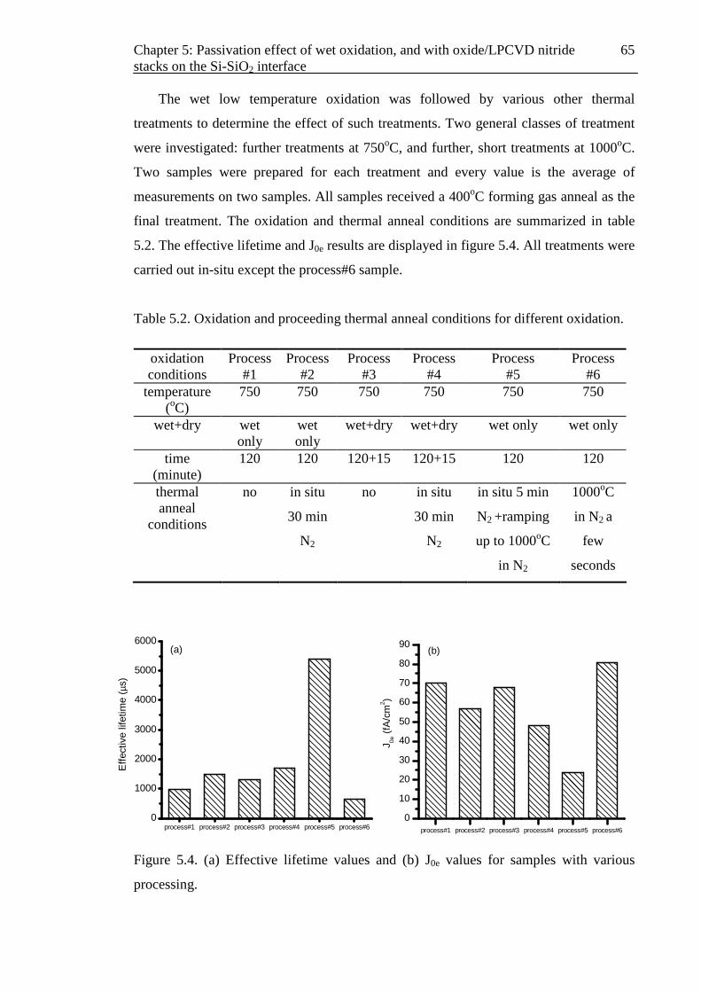
Chapter 5: Passivation effect of wet oxidation, and with oxide/LPCVD nitride stacks on the Si-SiO2 interface
65
process#1 process#2 process#3 process#4 process#5 process#6
0
10
20
30
40
50
60
70
80
90
J 0e (
fA/c
m2 )
(b)
process#1 process#2 process#3 process#4 process#5 process#60
1000
2000
3000
4000
5000
6000
Eff
ectiv
e lif
etim
e (µ
s)
(a)
The wet low temperature oxidation was followed by various other thermal
treatments to determine the effect of such treatments. Two general classes of treatment
were investigated: further treatments at 750oC, and further, short treatments at 1000oC.
Two samples were prepared for each treatment and every value is the average of
measurements on two samples. All samples received a 400oC forming gas anneal as the
final treatment. The oxidation and thermal anneal conditions are summarized in table
5.2. The effective lifetime and J0e results are displayed in figure 5.4. All treatments were
carried out in-situ except the process#6 sample.
Table 5.2. Oxidation and proceeding thermal anneal conditions for different oxidation.
Figure 5.4. (a) Effective lifetime values and (b) J0e values for samples with various
processing.
oxidation conditions
Process #1
Process #2
Process #3
Process #4
Process #5
Process #6
temperature (oC)
750 750 750 750 750 750
wet+dry wet only
wet only
wet+dry wet+dry wet only wet only
time (minute)
120 120 120+15 120+15 120 120
thermal anneal
conditions
no in situ
30 min
N2
no in situ
30 min
N2
in situ 5 min
N2 +ramping
up to 1000oC
in N2
1000oC
in N2 a
few
seconds
Chapter 5: Passivation effect of wet oxidation, and with oxide/LPCVD nitride stacks on the Si-SiO2 interface
66
It can be seen from figure 5.4 that following a 750oC wet oxidation with a N2
anneal at the same temperature results in some improvement of the interface – this is
consistent with findings on high temperature oxides. However, the passivation quality is
substantially worse than what can be achieved with a high temperature oxide. Short
thermal treatments at a high temperature are not sufficient to improve the interface. It
appears that treatments at higher temperatures need to be in the order of at least a few
minutes (such as during the ramp up to 1000oC) to give a benefit.
5.3 Effect of a phosphorous diffusion on the passivation
quality of the oxide
Work in this section is focused on further exploring the properties of thin oxides
grown at low temperature, especially at 750oC, and in particular, on better
understanding the effect of a phosphorous diffusion into the oxide.
5.3.1 Experimental details
A detailed description of effective lifetime and C-V measurements is given
previously. Samples used for the lifetime experiments received a standard light
phosphorous diffusion and oxidation. The oxide was then stripped by HF solution and
another wet oxide or dry oxide was grown at different temperatures. Following the
second oxidation, samples received a number of additional treatments for different
experiments.
5.3.2 Effect of a phosphorous diffusion into the thin oxide on
surface recombination
5.3.2.1 Effect on planar sample
After the first oxide layers were stripped using HF solution, second oxidations were
prepared as follows to get similar oxide thickness of about 30 nm:
w2: 2 hours wet oxidation + 15 minutes dry oxidation +30 minutes N2 all at 750oC
w4: 35 minutes wet oxidation + 15 minutes dry oxidation +30 minutes N2 all at 850oC

Chapter 5: Passivation effect of wet oxidation, and with oxide/LPCVD nitride stacks on the Si-SiO2 interface
67
w6: 21minutes dry oxidation +30 minutes N2 all at 1000oC
Following second oxidation, wafers received an FGA and the J0e values were
measured. Wafers were then subjected to another deep phosphorous diffusion (at 800oC
for 1 hour) and given another FGA, and J0e values were re-measured. Results are
summarised in table 5.3 below.
Table 5.3. J0e (fA/cm2) values of samples following various process steps.
It can be seen from table 5.3 that the phosphorous diffusion into the oxide reduced
surface recombination to a very low level, for low temperature oxides. The reduction is
unlikely to be simply due to the thermal treatment and seems to be linked to the
diffusion itself. It may be that the improvement is linked to changed oxide properties
(e.g. lower reflow temperature) due to the introduction of phosphorous.
In order to develop a better understanding of the effect of phosphorous diffusion on
surface recombination, several experiments were carried out with different oxide
thicknesses. The oxidation conditions and oxide thicknesses were:
1. 750oC: 1 hr wet oxidation + 15 min dry oxidation+ 30 min N2, thickness ~10nm
2. 750oC: 3.5 hr wet oxidation + 15 min dry oxidation+ 30 min N2, thickness
~52nm
3. 800oC: 28 min wet oxidation + 15 min dry oxidation+ 30 min N2, thickness
~21nm
Following oxidation, an identical phosphorous diffusion was carried out into the
oxide of the wafers, and the wafers then received an FGA treatment. In addition, sheet
resistance (Rs) measurements were carried out before and after the phosphorous
diffusion into the oxide by using a linear four-point probe. The J0e and Rs results are
summarized in table 5.4 below.
after first FGA after deep P diffusion+ FGA
w2 (750oC) 67 15
w4 (850oC) 22 14
w6 (1000oC) 16 18

Chapter 5: Passivation effect of wet oxidation, and with oxide/LPCVD nitride stacks on the Si-SiO2 interface
68
-1.5 -1.0 -0.5 0.0
0
500
1000
1500
2000
Cap
acita
nce
(pF
)
Applied voltage (V)
800oC wet oxidation and deep P diffusion
Table 5.4. J0e(fA/cm2), Sheet resistance Rs(Ω/) values before and after a phosphorous
diffusion into the oxide.
These results suggest that, once the phosphorous diffusion reaches the Si-SiO2
interface, indicated by a decrease of Rs after deep phosphorous diffusion, a dramatic
deterioration in interface passivation occurs resulting in an increase in recombination.
To complement the lifetime results, C-V measurements were carried out. Figure 5.5
shows an example of a HFCV curve following deep phosphorous diffusion into the
oxide, for the case where the phosphorous diffusion has gone through the oxide. Figure
5.6 compares the high frequency C-V curves for samples with a thin oxide (grown at
750oC wet oxidation for 2 hour followed by in situ 15 minutes dry oxidation and 30
minutes N2 anneal) with and without a phosphorous diffusion into the oxide (all samples
received an FGA prior to measurement). In this case, the oxide was chosen to be thick
enough that the phosphorous did not diffuse to the Si-SiO2 interface.
Figure 5.5. HFCV curve of thin oxide sample (800oC: wet oxidation 28 minutes+15
minutes dry oxidation+30 minutes N2) followed by phosphorous diffusion and FGA.
Sample
thickness
J0e before P
diffusion
J0e after P
diffusion
Rs before P
diffusion
Rs after P
diffusion
1. ~10nm 61 510 400 200
2. ~52nm 59 42 400 400
3. ~21nm 59 120 1100 400

Chapter 5: Passivation effect of wet oxidation, and with oxide/LPCVD nitride stacks on the Si-SiO2 interface
69
-4 -2 0 2
0
200
400
600
Cap
acita
nce
(pF
)
Applied voltage (V)
before deep P diffusionafter deep P diffusion
Figure 5.6. Comparison of HFCV curves of samples before and after deep phosphorous diffusion into the oxide.
It is worth to note that, following phosphorous diffusion into the oxide, it was not
possible to obtain QSCV curves because the oxide was too leaky. Comparison with the
no deep phosphorous diffused curve [fig 5.2(b)], the fig 5.5 shows significant
degradation of the interface, evidenced by the ‘stretch-out’ of the curve (ie the transition
from high to low capacitance is not as rapid).
It can be seen from figure 5.6 that the two curves are almost identical except for a
voltage shift of ~0.5V. This confirms that the phosphorous did not diffuse to the
interface. There is no indication that the phosphorous diffusion resulted in a reduction in
interface defect density, although a comparison of the HFCV curves above gives
somewhat limited sensitivity.
The major effect of the phosphorous diffusion therefore appears to be the
incorporation of more positive charge in the oxide. The increase in the effective charge
density (ie assuming that all of the charge is located near the Si-SiO2 interface) is
estimated to be ~4x1011cm-2.
From the above results we can make a conclusion that a phosphorous diffusion into
a thin oxide results in significant degradation to the Si-SiO2 interface, and an increase in
recombination, if the phosphorous reaches the interface. If the phosphorous does not
diffuse all the way to the interface, then the phosphorous diffusion can result in a
significant reduction in interface recombination. This reduction seems to be linked to a
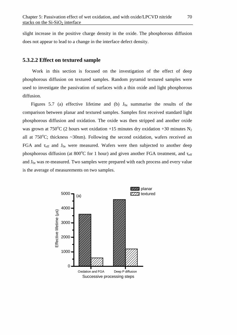
Chapter 5: Passivation effect of wet oxidation, and with oxide/LPCVD nitride stacks on the Si-SiO2 interface
70
Oxidation and FGA Deep P diffusion
0
1000
2000
3000
4000
5000
Effe
ctiv
e lif
etim
e (µ
s)
Successive processing steps
planar textured(a)
slight increase in the positive charge density in the oxide. The phosphorous diffusion
does not appear to lead to a change in the interface defect density.
5.3.2.2 Effect on textured sample
Work in this section is focused on the investigation of the effect of deep
phosphorous diffusion on textured samples. Random pyramid textured samples were
used to investigate the passivation of surfaces with a thin oxide and light phosphorous
diffusion.
Figures 5.7 (a) effective lifetime and (b) J0e summarise the results of the
comparison between planar and textured samples. Samples first received standard light
phosphorous diffusion and oxidation. The oxide was then stripped and another oxide
was grown at 750oC (2 hours wet oxidation +15 minutes dry oxidation +30 minutes N2
all at 750oC; thickness ~30nm). Following the second oxidation, wafers received an
FGA and τeff and J0e were measured. Wafers were then subjected to another deep
phosphorous diffusion (at 800oC for 1 hour) and given another FGA treatment, and τeff
and J0e was re-measured. Two samples were prepared with each process and every value
is the average of measurements on two samples.

Chapter 5: Passivation effect of wet oxidation, and with oxide/LPCVD nitride stacks on the Si-SiO2 interface
71
Oxidation and FGA Deep P diffusion
0
100
200
300
400
500
J 0e (
fA/c
m2 )
Successive processing steps
planar textured(b)
Figure 5.7. (a) Effective lifetime τ and (b) J0e of planar and textured samples following
various processing steps.
The above results show that textured samples show the same trend as planar
samples: a deep phosphorous diffusion into the oxide, which is not sufficient to reach
the Si-SiO2 interface, results in a moderate improvement to the interface (reduced J0e,
increased τeff). However, interface recombination for the textured samples is much
higher (by ~factor of 10) than for the planar ones.
5.4 Comparison of passivation effect of low
temperature wet oxidation on (100) and (111) Si-SiO2
interface
Work reported in the previous section shows that textured surfaces display much
greater interface recombination than identically processed planar equivalents. An
important question is whether this degradation is related to the particular crystal
orientation (ie near (111) orientation for random texture) or to the presence of corners
and edges on textured surfaces, which may result in high localized stresses and defects.
In this section, we compared (100) and (111) oriented, planar samples oxidized at 750
or 850oC. The results show that the (111) crystal orientation is to a large extent

Chapter 5: Passivation effect of wet oxidation, and with oxide/LPCVD nitride stacks on the Si-SiO2 interface
72
1 2100
1000
10000
Effe
ctiv
e lif
etim
e (µ
s)
Processing steps
750oC (100) 750oC (111) 850oC (100) 850oC (111)
(a)
responsible for the much worse passivation of random textured surfaces. It is therefore
possible that textures which largely avoid exposing (111) planes may be able to achieve
much better passivation.
5.4.1 Experimental details
Samples used for lifetime experiments received a standard light phosphorous
diffusion and oxidation first. The oxide was then stripped and another oxide was grown.
The second oxide was prepared at 750oC (80 minutes wet oxidation +30 minutes N2 all
at 750oC; thickness ~20nm) or 850oC (10 minutes wet oxidation + 30 minutes N2 all at
850oC; thickness ~30nm). The (100) samples were FZ, p-type, ~100Ω.cm and (111)
samples were FZ, n-type, (~60Ω.cm)
Following oxidation, wafers received an FGA, and τeff and J0e were measured. The
results are shown in figure 5.8.
5.4.2 Effect of surface orientation and oxidation temperature
The results in figure 5.8 are in broad agreement with those previously obtained for
similarly processed samples (see for example results in figure 5.1 for planar samples
with a 750oC oxide). J0e values for (100) samples with 850oC oxide are somewhat
higher than previously measured.
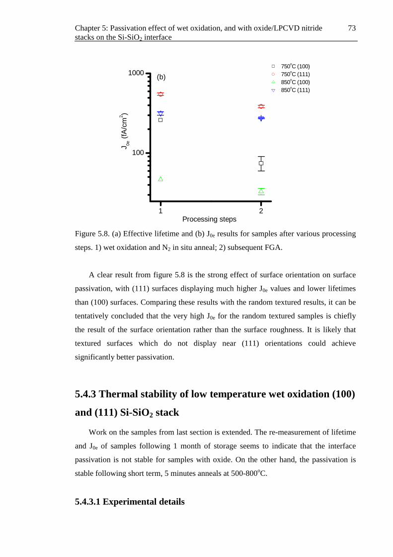
Chapter 5: Passivation effect of wet oxidation, and with oxide/LPCVD nitride stacks on the Si-SiO2 interface
73
1 2
100
1000
J 0e (
fA/c
m2 )
Processing steps
750oC (100) 750oC (111) 850oC (100) 850oC (111)
(b)
Figure 5.8. (a) Effective lifetime and (b) J0e results for samples after various processing
steps. 1) wet oxidation and N2 in situ anneal; 2) subsequent FGA.
A clear result from figure 5.8 is the strong effect of surface orientation on surface
passivation, with (111) surfaces displaying much higher J0e values and lower lifetimes
than (100) surfaces. Comparing these results with the random textured results, it can be
tentatively concluded that the very high J0e for the random textured samples is chiefly
the result of the surface orientation rather than the surface roughness. It is likely that
textured surfaces which do not display near (111) orientations could achieve
significantly better passivation.
5.4.3 Thermal stability of low temperature wet oxidation (100)
and (111) Si-SiO2 stack
Work on the samples from last section is extended. The re-measurement of lifetime
and J0e of samples following 1 month of storage seems to indicate that the interface
passivation is not stable for samples with oxide. On the other hand, the passivation is
stable following short term, 5 minutes anneals at 500-800oC.
5.4.3.1 Experimental details

Chapter 5: Passivation effect of wet oxidation, and with oxide/LPCVD nitride stacks on the Si-SiO2 interface
74
1 2 3 4100
1000
10000
Effe
ctiv
e lif
etim
e (µ
s)
Processing steps
750oC (100) 750oC (111) 850oC (100) 850oC (111)
(a)
Samples previously prepared and measured, as described in the last section, were
used for experiments. No further treatment had been carried out on these samples. Other
samples received RTA in a N2 atmosphere for 3 minutes at temperatures between 500
and 800oC, in order to determine the thermal stability of the passivation.
It should be noted that the RTA treatments are quite different in their effect from
the N2 anneals following oxidation. This is because the RTA treatments are carried out
in sealed systems in which no moisture can enter. In contrast, the oxidations and
subsequent anneals are done in a tube furnace which is not completely sealed. There is
thus the possibility that moisture from the air will enter the furnace and influence the
results. Reliable results are therefore best obtained by first passivating samples with an
FGA and then, if required, carrying out depassivating treatments in an RTA system.
5.4.3.2 Stability of lifetime and J0e of samples following FGA
Figure 5.9 shows the lifetime and J0e values of the control samples. It can be seen
that the surface passivation of some of the samples does not appear stable. This is
particularly the case for the (100) samples with a 750oC oxide.

Chapter 5: Passivation effect of wet oxidation, and with oxide/LPCVD nitride stacks on the Si-SiO2 interface
75
1 2 3 4
100
1000
J 0e (
fA/c
m2 )
Processing steps
750oC (100) 750oC (111) 850oC (100) 850oC (111)
(b)
1 2 3 4 5 6100
1000
10000
Effe
ctiv
e lif
etim
e (µ
s)
Processing steps
750oC (100) 750oC (111) 850oC (100) 850oC (111)
(a)
Figure 5.9. (a) Effective lifetime and (b) J0e results for samples after various processing
steps. 1) Wet oxidation and N2 anneal; 2) subsequent FGA; 3) repeat of measurement 3
days later; 4) repeat of measurement 40 days storage in N2.
5.4.3.3 Stability of lifetime and J0e of samples following RTA
Figure 5.10 shows the change in effective lifetime and J0e with subsequent RTA
treatments.

Chapter 5: Passivation effect of wet oxidation, and with oxide/LPCVD nitride stacks on the Si-SiO2 interface
76
1 2 3 4 5 610
100
1000
J 0e (
fA/c
m2 )
Processing steps
750oC (100) 750oC (111) 850oC (100) 850oC (111)
(b)
Figure 5.10. The evolution of (a) effective lifetime and (b) J0e with process treatments. 1)
oxidation and in situ N2 anneal; 2) subsequent FGA; (3)-(6) subsequent RTA treatments
at 500, 600, 700 and 800oC for 3 minutes, respectively. Data points for (1) and (2) are
the averages of all the samples. Data points for (3) to (6) come from different samples ie
the RTA treatments were not cumulative.
It can be seen from fig 5.10 that all samples show a strong degradation in surface
passivation even following a relatively low temperature treatment at 500oC. The
difference between (100) and (111) samples becomes substantially less following the
RTA treatments. In other words, while the (100) surfaces can be passivated much more
effectively, this passivation is quite easily destroyed by thermal treatments.
5.5 Passivation effect of oxide/nitride stacks on Si-SiO2
interface
5.5.1 Effect of LPCVD nitride deposition temperature on
surface passivation of Si-SiO2 stack
Previous work [113] has shown that a thin SiO2 layer should be grown before
LPCVD Si3N4 deposition to prevent irreversible bulk damage caused by stress from the
nitride layer. Such LPCVD Si3N4/SiO2/Si stacks can act as effective antireflection

Chapter 5: Passivation effect of wet oxidation, and with oxide/LPCVD nitride stacks on the Si-SiO2 interface
77
coatings and simultaneously allow good surface passivation to be achieved. Of
particular interest for potential photovoltaic applications is the recombination rate of
minority carriers at the interface. In our work, we have found that the deposition
temperature has a tremendous impact on surface passivation, with high temperatures
leading to much higher values of the emitter saturation current J0e.
Samples used for the experiments received a standard light phosphorous diffusion,
followed by an oxidation at 1000oC for 1 hour, 30 minutes in situ N2 anneal and FGA
successively with oxide thickness about 50nm. ~50nm of LPCVD Si3N4 was then
deposited at 775 or 825oC. The LPCVD nitride layer (but not the oxide) was then
stripped in hot phosphoric acid at 170oC, and the samples were given another FGA
treatment. Table 5.5 summarizes the results following different processing steps.
Table 5.5. Effective lifetimeτ(µs) and J0e(fA/cm2) values following various process
steps. 1. oxidized and FGA, 2. LPCVD deposition, 3. strip nitride, 4. FGA again.
The results of the effective lifetimes at the beginning and end of the process (steps
1 and 4) show that there has been some degradation to the Si bulk. The degradation is
clearly in the bulk, and not at the surfaces (as can be seen from the J0e values). There are
two possible degradation mechanisms – 1) contamination and 2) introduction of defects
due to the presence of the nitride film. Previous experiments have shown that the
presence of a nitride layer does cause irreversible bulk damage, and that at least some of
this damage is almost certainly due to defect generation resulting from the presence of a
nitride layer [114]. The extent of the bulk degradation was observed to depend on
Step 1 Step2 Step3 Step4
825oC LPCVD
Si3N4
τ 5100 1700 1400 4000
J0e 16 190 210 25
775oC LPCVD
Si3N4
τ 4800 4100 460 1000
J0e 21 38 400 20

Chapter 5: Passivation effect of wet oxidation, and with oxide/LPCVD nitride stacks on the Si-SiO2 interface
78
interfacial oxide thickness, with even a relatively thin (~25nm) oxide reducing the bulk
degradation to very low levels.
The degradation observed here is more likely to be due to contamination, since the
oxide was relatively thick and the degradation is quite severe. Nevertheless, effective
lifetimes at the end of the process are still high enough that the results relating to
surface passivation can be interpreted without difficulty.
The J0e results in table 5.5 indicate that J0e depends sensitively on deposition
temperature (compare J0e values in tables at step 2). Nitride deposition has two effects
on the Si-SiO2 interface: 1) it leads to the generation of some additional defects; and 2)
it causes the de-passivation of previously passivated defects. The fact that the final J0e
values (step 4, following re-hydrogenation of interface defects) are comparable to the
initial values (step 1) for both deposition temperatures suggests that effect (1) is
dominant. Note that the error in J0e measurements is typically +/- 10%. A higher furnace
temperature will lead to a greater loss of hydrogen from the interface prior (and
probably also during) nitride layer deposition. Hence, the nitride deposition temperature
is a critical parameter.
5.5.2 Effect of LPCVD nitride deposition on surface
passivation of Si-SiO2 stack
In this section, the effect of LPCVD nitride deposition on surface recombination
was examined for various oxides. Lifetime/J0e values were measured at various stages
during the process sequence. Oxidation conditions for the different samples were as
follows to achieve nearly identical oxide thickness about 30 nm:
w1: 2 hours wet oxidation + 15 minutes dry oxidation +30 minutes N2 all at 750oC
w3: 35 minutes wet oxidation + 15 minutes dry oxidation +30 minutes N2 all at 850oC
w5: 21 minutes dry oxidation +30 minutes N2 all at 1000oC
Table 5.6 summarises J0e results following various processing steps. J0e was
measured after forming gas anneal; after LPCVD nitride deposition at 775oC; and after
a subsequent N2 anneal at 900oC for 30 minutes (to simulate possible subsequent high
temperature steps).
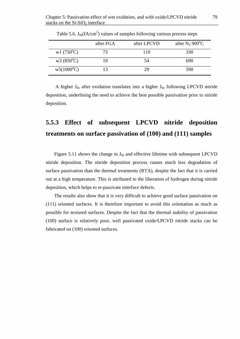
Chapter 5: Passivation effect of wet oxidation, and with oxide/LPCVD nitride stacks on the Si-SiO2 interface
79
Table 5.6. J0e(fA/cm2) values of samples following various process steps
A higher J0e after oxidation translates into a higher J0e following LPCVD nitride
deposition, underlining the need to achieve the best possible passivation prior to nitride
deposition.
5.5.3 Effect of subsequent LPCVD nitride deposition
treatments on surface passivation of (100) and (111) samples
Figure 5.11 shows the change in J0e and effective lifetime with subsequent LPCVD
nitride deposition. The nitride deposition process causes much less degradation of
surface passivation than the thermal treatments (RTA), despite the fact that it is carried
out at a high temperature. This is attributed to the liberation of hydrogen during nitride
deposition, which helps to re-passivate interface defects.
The results also show that it is very difficult to achieve good surface passivation on
(111) oriented surfaces. It is therefore important to avoid this orientation as much as
possible for textured surfaces. Despite the fact that the thermal stability of passivation
(100) surface is relatively poor, well passivated oxide/LPCVD nitride stacks can be
fabricated on (100) oriented surfaces.
after FGA after LPCVD after N2 900oC
w1 (750oC) 73 110 330
w3 (850oC) 19 54 690
w5(1000oC) 13 29 590

Chapter 5: Passivation effect of wet oxidation, and with oxide/LPCVD nitride stacks on the Si-SiO2 interface
80
1 2 310
100
1000
J 0e (
fA/c
m2 )
Processing steps
750 oC (100) 750 oC (111) 850 oC (100) 850 oC (111)
(b)
1 2 3100
1000
10000
Effe
ctiv
e lif
etim
e (µ
s)
Processing steps
750 oC (100) 750 oC (111) 850 oC (100) 850 oC (111)
(a)
Figure 5.11. Evolution of (a) effective lifetime and (b) J0e with process treatments. (1)
oxidation and in situ N2 anneal; (2) subsequent FGA; (3) subsequent LPCVD nitride
deposition.
In order to better understand the difference between (100) and (111) Si-SiO2 stack
for LPCVD Si3N4 deposition, LPCVD Si3N4 was deposited on some previously
depassivated samples using RTAs at various temperatures (figure 5.10). Figure 5.12 and
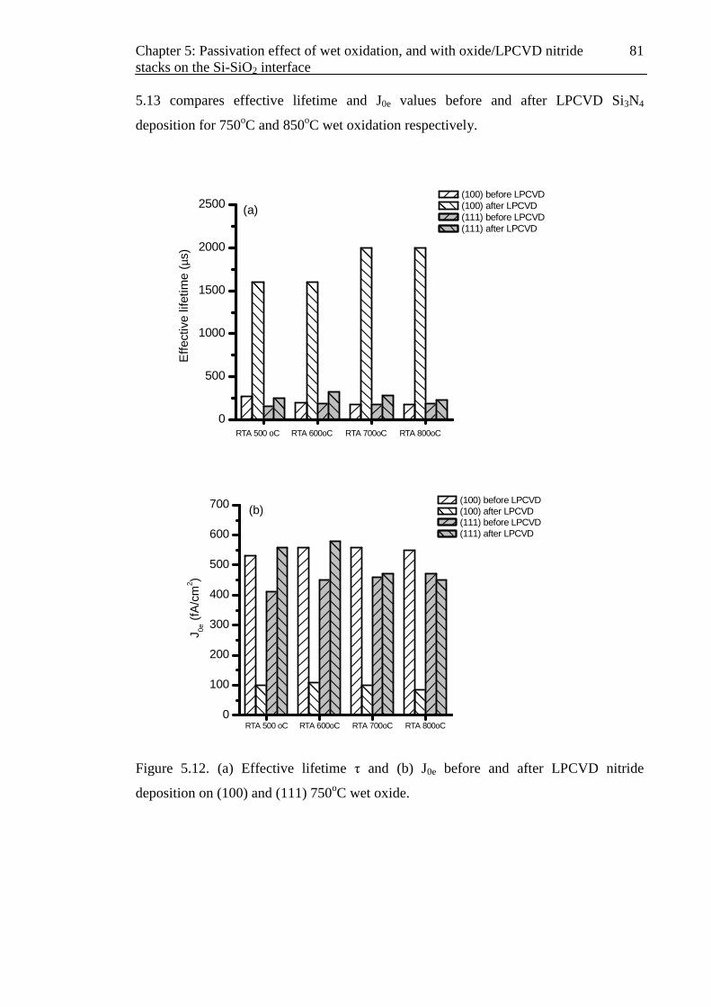
Chapter 5: Passivation effect of wet oxidation, and with oxide/LPCVD nitride stacks on the Si-SiO2 interface
81
RTA 500 oC RTA 600oC RTA 700oC RTA 800oC0
100
200
300
400
500
600
700
J 0e (
fA/c
m2 )
(100) before LPCVD (100) after LPCVD (111) before LPCVD (111) after LPCVD
(b)
RTA 500 oC RTA 600oC RTA 700oC RTA 800oC
0
500
1000
1500
2000
2500
Effe
ctiv
e lif
etim
e (µ
s) (100) before LPCVD (100) after LPCVD (111) before LPCVD (111) after LPCVD
(a)
5.13 compares effective lifetime and J0e values before and after LPCVD Si3N4
deposition for 750oC and 850oC wet oxidation respectively.
Figure 5.12. (a) Effective lifetime τ and (b) J0e before and after LPCVD nitride
deposition on (100) and (111) 750oC wet oxide.

Chapter 5: Passivation effect of wet oxidation, and with oxide/LPCVD nitride stacks on the Si-SiO2 interface
82
RTA 500 oC RTA 600oC RTA 700oC RTA 800oC0
500
1000
1500
2000
2500
3000
Effe
ctiv
e lif
etim
e (µ
s)
(100) before LPCVD (100) after LPCVD (111) before LPCVD (111) after LPCVD
(a)
RTA 500 oC RTA 600oC RTA 700oC RTA 800oC0
100
200
300
400
500
600
700
J 0e (
fA/c
m2 )
(100) before LPCVD (100) after LPCVD (111) before LPCVD (111) after LPCVD
(b)
Figure 5.13. (a) Effective lifetime τ and (b) J0e before and after LPCVD nitride
deposition on (100) and (111) 850oC wet oxide.
It can be seen from figure 5.12 and 5.13 that, following nitride deposition on either
750oC wet oxide or 850oC wet oxide, the (100) samples have improved substantially,
while the (111) samples have not.
The above results suggest that, for the samples investigated, the (111) surface does
not display inherently worse recombination if all the defects are unpassivated. Instead,
the major difference is the ability to passivate interface defects with hydrogen. While

Chapter 5: Passivation effect of wet oxidation, and with oxide/LPCVD nitride stacks on the Si-SiO2 interface
83
1 2 3 4100
1000
10000
Effe
ctiv
e lif
etim
e (µ
s)
Processing steps
750 oC (100) 750 oC (111) 850 oC (100) 850 oC (111)
(a)
the (100) interface defects can be passivated reasonably well using either an FGA or
with hydrogen from another source (such as from a H containing film), a large fraction
of the (111) defects are not able to be passivated in this way. This behaviour is similar
as the behaviour observed for higher temperature oxides.
5.5.4 Thermal stability of samples with oxide/LPCVD nitride
stacks
Samples which previously had LPCVD nitride deposited were re-measured in order
to determine if there was any degradation after 40 days storage at room temperature.
The results are shown in figure 5.14. The trend is similar to that in figure 5.9, with
apparently significant degradation in surface passivation for the (100) samples but no
significant degradation for the (111) samples. However, there is significant variation in
the response of identically prepared samples, especially in the J0e for (100) samples with
750oC oxide.
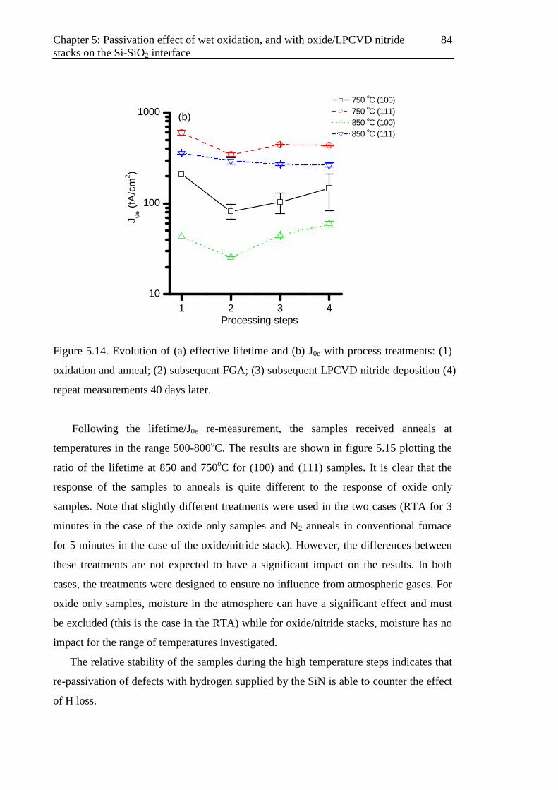
Chapter 5: Passivation effect of wet oxidation, and with oxide/LPCVD nitride stacks on the Si-SiO2 interface
84
1 2 3 410
100
1000
J 0e (
fA/c
m2 )
Processing steps
750 oC (100) 750 oC (111) 850 oC (100) 850 oC (111)
(b)
Figure 5.14. Evolution of (a) effective lifetime and (b) J0e with process treatments: (1)
oxidation and anneal; (2) subsequent FGA; (3) subsequent LPCVD nitride deposition (4)
repeat measurements 40 days later.
Following the lifetime/J0e re-measurement, the samples received anneals at
temperatures in the range 500-800oC. The results are shown in figure 5.15 plotting the
ratio of the lifetime at 850 and 750oC for (100) and (111) samples. It is clear that the
response of the samples to anneals is quite different to the response of oxide only
samples. Note that slightly different treatments were used in the two cases (RTA for 3
minutes in the case of the oxide only samples and N2 anneals in conventional furnace
for 5 minutes in the case of the oxide/nitride stack). However, the differences between
these treatments are not expected to have a significant impact on the results. In both
cases, the treatments were designed to ensure no influence from atmospheric gases. For
oxide only samples, moisture in the atmosphere can have a significant effect and must
be excluded (this is the case in the RTA) while for oxide/nitride stacks, moisture has no
impact for the range of temperatures investigated.
The relative stability of the samples during the high temperature steps indicates that
re-passivation of defects with hydrogen supplied by the SiN is able to counter the effect
of H loss.

Chapter 5: Passivation effect of wet oxidation, and with oxide/LPCVD nitride stacks on the Si-SiO2 interface
85
1 2 3 4 50.2
0.3
0.4
0.5
0.6
0.7
0.8
J 0e r
atio
Processing steps
(100)850oC
/(100)750oC
(111)850oC
/(111)750oC
(b)
1 2 3 4 5
0.8
1.2
1.6
2.0
2.4
Life
time
ratio
Processing steps
(100)850oC
/(100)750oC
(111)850oC
/(111)750oC
(a)
Figure 5.15. Evolution of (a) effective lifetime ratio and (b) J0e ratio with process
treatments. (1) oxidation and anneal and LPCVD (50nm); (2)-(5) subsequent N2 anneal
treatments at 500, 600, 700 and 800oC for 5 minutes, respectively. Treatments are
cumulative.
The results indicate that good, stable surface passivation using low temperature
thermal oxides is difficult to achieve. Surfaces with a (111) orientation can not be well
Chapter 5: Passivation effect of wet oxidation, and with oxide/LPCVD nitride stacks on the Si-SiO2 interface
86
passivated even following a forming gas anneal. Surfaces with a (100) orientation can
be relatively well passivated, particularly if the oxidation temperature is 850oC (or
above). However, even at this temperature, the passivation does not appear to be
completely stable when the sample is stored in the dark at room temperature in N2
atmosphere. This result also holds for oxide/nitride stacks. In addition, the (100)
samples appear to not be stable at room temperature, but actually show reasonable
stability during anneals at moderate temperatures. This suggests that the main problem
is that some interface defects depassivated over time even at room temperature. At
elevated temperatures, the reasonable stability is likely the result of the release of
atomic hydrogen from the LPCVD layer which re-passivated defects.
The thermal stability of (100) oxide only samples is much poorer than of samples
with a high temperature nitride, indicating a rapid loss of hydrogen from the interface at
temperatures of 500oC and above. However, the degradation resulting from the
deposition of an LPCVD nitride layer, and from subsequent high temperature treatments
for moderate periods of time, is small due to the simultaneous re-passivation with
atomic hydrogen from the nitride film.
5.6 Summary
The work in this section has investigated the passivation that can be achieved with
relatively low temperature, thin thermal oxides (grown in the temperature range 750-
900oC), and with oxide/LPCVD nitride stacks. The results can be summarized as
follows:
For thin oxides, firstly, higher oxidation temperature results in better surface
passivation. A reasonable compromise may be a temperature of ~850oC. The lower the
temperature, the poorer the surface passivation and the stability of the surface
passivation will be. Secondly, surface orientation has a large effect on achievable
surface passivation. (111) surfaces display high recombination rates even at an
oxidation temperature of 850oC and following an FGA. Surfaces with (111) orientation
are therefore undesirable, and surface textures which avoid this orientation are likely to
offer better passivation. Thirdly, the diffusion of phosphorous into the oxide results in a
significant improvement in surface passivation. However, this improvement appears to
be related to a slight increase in positive charge density in the oxide rather than to a
decrease in the unpassivated interface defect density. Since surface passivation

Chapter 5: Passivation effect of wet oxidation, and with oxide/LPCVD nitride stacks on the Si-SiO2 interface
87
deteriorates markedly if the diffusion reaches the interface, this is unlikely to be a
practical process.
On the other hand, for oxide/nitride stacks, firstly, the nitride deposition
temperature should be kept as low as possible in order to retain good surface passivation
following nitride deposition. A practical temperature may be in the range 750-775oC. In
this temperature range, the degradation in surface passivation is small. Secondly, the
thermal stability of the surface passivation is much better than for samples with an
oxide only, due to the presence of hydrogen in the nitride which re-passivates interface
defects. Thirdly, even for oxide/nitride stacks, the passivation does not seem to be stable.
Further experiments would be required to definitively establish that the measured
changes in effective lifetime and J0e, at room temperature, are due to interface
degradation.

Chapter 5: Passivation effect of wet oxidation, and with oxide/LPCVD nitride stacks on the Si-SiO2 interface
88

Chapter 6: Influence of atomic hydrogen exposure on the Si-SiO2 interface
89
CHAPTER 6
Influence of atomic hydrogen exposure
on the Si-SiO2 interface
In this chapter, the influence of atomic hydrogen on the surface passivation of the
Si-SiO2 interface is investigated. Atomic hydrogen is mainly produced in a remote
PECVD system using RF or MW power. Inductively coupled photoconductivity decay
measurements indicate an increase in carrier recombination at the surfaces following
atomic hydrogen exposure, as measured by an increase in the emitter saturation current
density. These defects are not thermally stable and are removed by subsequent thermal
treatments above 240oC in N2. In addition, atomic hydrogen results in the passivation of
a certain fraction of thermally stable interface defects. However, the fraction of defects
passivated is always lower than can be achieved by exposure to molecular hydrogen.
Variation of sample temperature during atomic H exposure in the range 25-600oC does
not have a significant impact on the passivation efficiency.

Chapter 6: Influence of atomic hydrogen exposure on the Si-SiO2 interface
90
6.1 Experimental details
Lifetime and C-V samples received standard processing steps. Annealing in forming
gas at 400oC was performed to hydrogenate the Si-SiO2 interface of some samples,
while others samples were dehydrogenated by a rapid RTA at 700oC for 3 minutes in N2.
The samples were exposed to atomic H in the PECVD reactor. For some samples, a
2.45GHz microwave plasma was used for atomic hydrogen generation while for others
a 13.56MHz RF source was used. For both sources, the source frequency is sufficiently
high that no ion bombardment of the substrate is expected. The penetration of hydrogen
to the Si-SiO2 interface is therefore by diffusion rather than by ion bombardment [115].
The standard plasma conditions used in this chapter for MW power are: MW power
200W, pressure 0.2mbar, time 5 minutes/side, room temperature and H2 flow rate 150
Standard Cubic Centimeters per Minute (sccm) whereas the plasma conditions for RF
plasma power are: RF power 300W, pressure 0.05mbar, time 5 minutes/side, room
temperature and H2 flow rate 150sccm. For the symmetrical photo-conductance samples,
both sides were exposed, while in the case of CV samples, just the polished side was
exposed.
After plasma exposure, an RTA was carried out at temperatures in the range 25-
400oC for up to 3 minutes in N2 to remove plasma-induced defects. Subsequently, an
FGA treatment was carried out at 400oC for 30 minutes, which has the effect of re-
hydrogenating the interface and thus rendering the majority of residual defects
electrically inactive. In addition, an alternative thermal anneal technique by using a
TIDLS lifetime tester was also applied to investigate the properties of Si-SiO2 interface
at temperatures in the range 120-240oC in air or N2 atmosphere.
Lifetime measurements were carried out using the inductively coupled
photoconductivity measurement technique [59, 116]. The value of the emitter saturation
current density J0e was extracted from measurements of the effective carrier lifetime in
high injection, as described in detail in chapter 3.
Prior to C-V measurements, about 80nm Aluminium was deposited with an area of
around 4.7×10⁻³cm2 through a shadow mask on the oxide to form a MOS structure. This
is done in a vacuum chamber at pressure lower than 3×10⁻⁶torr and the thickness of
metal is accurately controlled. High-Frequency C-V (HFCV) measurements were
carried out at 1 MHz, and Quasi-Static C-V (QSCV) measurements were carried out at
0.01Hz, with a sweep rate of 50mV/s. The charge density in the oxide layers is deduced
from the flat-band voltage of curves (HFCV) at 1MHz. The Si-SiO2 interface defect
Chapter 6: Influence of atomic hydrogen exposure on the Si-SiO2 interface
91
density is calculated by joint HFCV and QSCV measurements using the method of
Castagne and Vapaille [85].
The use of different substrates was dictated by the requirements of the
characterization techniques. For C-V measurements, moderately doped wafers are
required for accurate results, while the unambiguous extraction of the emitter saturation
current J0e requires the use of lightly doped material as well as diffused surfaces,
because extraction of J0e requires measurement with the wafer bulk in high-level
injection but the surfaces in low-level injection.
6.2 Background tests
6.2.1 Effect of molecular H2 on the Si-SiO2 interface
Figure 6.1 shows the C-V curves of (a) depassivated and (b) passivated samples
after molecular hydrogen exposure in the PECVD reactor chamber at pressure 0.05mbar,
gas flow rate 150sccm and time 5 minutes/side at room temperature and 400oC,
respectively. For comparison, the corresponding curves for depassivated and passivated
samples without H2 exposure are also shown in figure 6.1 (a) and (b), respectively.
Methods of hydrogenation and dehydrogenation to the Si-SiO2 stacks are described
above. Figure 6.2 shows the corresponding Dit distributions for the samples in fig 6.1 (a),
extracted using the curves from fig. 6.1 (a). Table 6.1 summarizes the J0e results of an
initially passivated sample after molecular hydrogen exposure at the pressure 0.2mbar,
gas flow rate 150sccm and time 5 minutes at 400oC in the PECVD reactor chamber. The
samples were then rinsed in an isopropanol (IPA) solution and water to remove the
surface charges. After that, another FGA treatment was performed.

Chapter 6: Influence of atomic hydrogen exposure on the Si-SiO2 interface
92
-6 -4 -2 0 20.0
0.2
0.4
0.6
0.8
1.0C
/Ci
Applied voltage (V)
depassivated control HFCVdepassivated control QSCV
25oC H2 5min HFCV
25oC H2 5min QSCV
400oC H2 5min HFCV
400oC H2 5min QSCV
(a)
-6 -4 -2 0 20.0
0.2
0.4
0.6
0.8
1.0
C/C
i
Applied voltage (V)
passivated control HFCV passivated control QSCV
25oC 5min H2 HFCV
25oC 5min H2 QSCV
400oC 5min H2 HFCV
400oC 5min H2 QSCV
(b)
Figure 6.1. C-V curves for (a) depassivated samples and (b) passivated samples, before
H2 exposure, after room temperature 5 minutes H2 exposure, and after 400oC, 5 minutes
H2 exposure respectively.
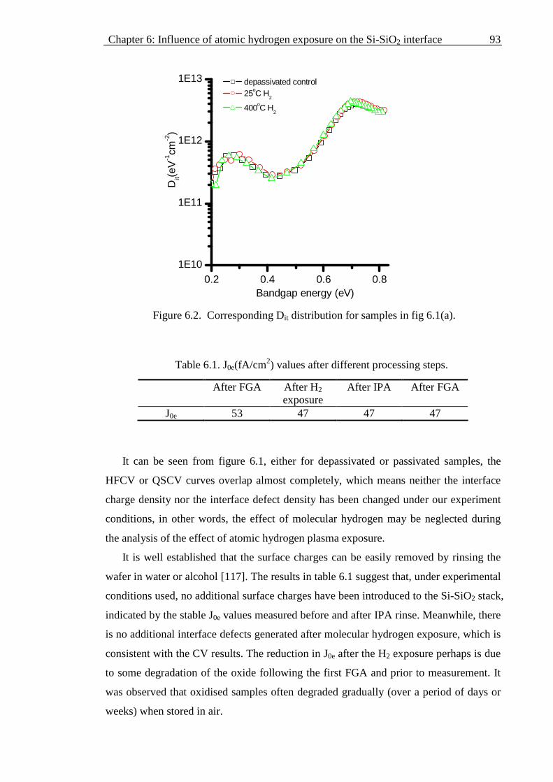
Chapter 6: Influence of atomic hydrogen exposure on the Si-SiO2 interface
93
0.2 0.4 0.6 0.81E10
1E11
1E12
1E13
Dit(
eV-1cm
-2)
Bandgap energy (eV)
depassivated control 25oC H
2
400oC H2
Figure 6.2. Corresponding Dit distribution for samples in fig 6.1(a).
Table 6.1. J0e(fA/cm2) values after different processing steps.
It can be seen from figure 6.1, either for depassivated or passivated samples, the
HFCV or QSCV curves overlap almost completely, which means neither the interface
charge density nor the interface defect density has been changed under our experiment
conditions, in other words, the effect of molecular hydrogen may be neglected during
the analysis of the effect of atomic hydrogen plasma exposure.
It is well established that the surface charges can be easily removed by rinsing the
wafer in water or alcohol [117]. The results in table 6.1 suggest that, under experimental
conditions used, no additional surface charges have been introduced to the Si-SiO2 stack,
indicated by the stable J0e values measured before and after IPA rinse. Meanwhile, there
is no additional interface defects generated after molecular hydrogen exposure, which is
consistent with the CV results. The reduction in J0e after the H2 exposure perhaps is due
to some degradation of the oxide following the first FGA and prior to measurement. It
was observed that oxidised samples often degraded gradually (over a period of days or
weeks) when stored in air.
After FGA After H2 exposure
After IPA After FGA
J0e 53 47 47 47

Chapter 6: Influence of atomic hydrogen exposure on the Si-SiO2 interface
94
0 30 60 90 120 150 180
50
60
70
80
90
100
J 0e(f
A/c
m2 )
Time (s)
sandwiched without sandwiched
6.2.2 Effect of illumination during RTA
Following H plasma exposure, selected samples were annealed in an RTA furnace.
The RTA chamber heats the samples by irradiating them with intense light overing a
broad spectrum of wavelengths. The RTA process is therefore not a purely thermal
process; the high energy photons produced may also result in changes at the Si-SiO2
interface. Since anneals were generally carried out at low temperatures (in the range
100-400oC) the lamps generate far lower fluxes of high energy photons than at higher
energies, and therefore the effect of illumination during RTA treatments is likely to be
negligible. To confirm this, samples that had been exposed to a H plasma (introducing
thermally unstable defects) were annealed in the RTA furnace. One sample was
sandwiched between two Si wafers (thus eliminating any effect due to illumination)
while another sample was not. Samples were heated to 200oC for times ranging from 5
to 180 seconds (cumulative). The low temperature was chosen to allow the annealing
behaviour to be observed. After that, the same samples received a 400oC, 10 second
RTA treatment. Figure 6.3 shows the results following 200oC RTA, the J0e values at
zero annealing time come from samples that just received hydrogen plasma exposure.
Figure 6.3. J0e values of MW hydrogen plasma exposed samples after RTA in N2 at
200oC with time range from 5 to 180 seconds.
It can be seen from fig 6.3 that both samples show a similar trend. After the 200oC
RTA treatment, the J0e values for sandwiched and bare samples are 58fA/cm2 and

Chapter 6: Influence of atomic hydrogen exposure on the Si-SiO2 interface
95
52fA/cm2 respectively. Following a 400oC RTA for 10 seconds, the J0e values for both
sandwiched and bare samples decreased to about 35fA/cm2. From these results, it
appears that the illumination during RTA at low temperatures does not have any impact
on the annealing of the thermally unstable interface defects. All RTA treatments in this
thesis were carried out for samples without sandwich structure.
6.3 Effect of RTA on the Si-SiO2 interface following
atomic hydrogen plasma exposure
In this section, the effect of RTA treatments following hydrogen plasma exposure
on the Si-SiO2 interface properties is discussed. RTAs in dry nitrogen gas were carried
out at different temperatures from 100oC to 400oC for up to 180 seconds. The difference
of the effect of RTA at 300oC and 400oC was compared. Samples just after RF or MW
hydrogen plasma exposure under standard conditions were investigated respectively.
Initially hydrogenated and dehydrogenated samples were used for plasma exposure
treatments and subsequent RTA treatments.
6.3.1 RF power
Figure 6.4 shows the dependence of (a) effective lifetime τ and (b) corresponding
J0e on RTA time and temperature for RF hydrogen plasma exposed samples. Four
passivated samples, with initial J0e values between 58 to 72fA/cm2, were used for the
RTA curves following a RF hydrogen plasma exposure under the standard conditions.
The bottom straight dashed line in fig 6.4 (b) represents the average initial J0e values
before RF hydrogen plasma exposure. The values at time zero are from just after
hydrogen plasma exposure. Figure 6.5 illustrates the effects of atomic H plasma
exposure and subsequent RTA on the CV characteristics, measured on p-type MOS
stacks (note that in all cases, the metal to form the MOS structure was evaporated just
prior to measurement). Figure 6.6 shows the corresponding Dit distribution. Three
passivated samples were used. Figure 6.7 shows the C-V results for initially
depassivated, p-type MOS stacks subjected to otherwise identical processing treatments
as the samples fig 6.5. Figure 6.8 shows the corresponding Dit distribution. Three
depassivated samples were used. RF hydrogen plasma exposure conditions are standard
and RTA at 400oC in N2 for 3 minutes. For comparison, the corresponding curves for an

Chapter 6: Influence of atomic hydrogen exposure on the Si-SiO2 interface
96
0 30 60 90 120 150 180
100
1000
J 0e(f
A/c
m2 )
Time (s)
100oC RTA200oC RTA300oC RTA400oC RTA
(b)
0 30 60 90 120 150 180100
1000
10000E
ffec
tive
lifet
ime
(µs)
Time (s)
100oC RTA200oC RTA300oC RTA400oC RTA
(a)
as oxidized and forming gas annealed MOS stack as well as an as oxidized and RTA
700oC de-hydrogenated MOS stack are also shown in fig 6.5 and 6.7 respectively.
Figure 6.4. (a) Effective lifetime τ and (b) Emitter saturation current density J0e for
initially RF atomic hydrogen exposed samples as a function of RTA annealing
temperature and time.
It can be seen from figure 6.4 that the majority of the H-generated defects appears to
be rapidly removed by anneals at a temperature of 300oC and above (these anneals do
not influence the Pbx defects that always exist at a thermally grown Si-SiO2 interface [55,
118]. Further, the J0e values do not return to their initial values which indicates that

Chapter 6: Influence of atomic hydrogen exposure on the Si-SiO2 interface
97
-20 -15 -10 -5 0 50.0
0.2
0.4
0.6
0.8
1.0
C/C
i
Applied voltage (V)
HFCV passivated control HFCV RF H plasma HFCV RF H plasma and 400oC RTA
(a)
-20 -15 -10 -5 0 50.0
0.2
0.4
0.6
0.8
1.0
C/C
i
Applied voltage (V)
QSCV passivated control QSCV RF H plasma QSCV RF H plasma and 400oC RTA
(b)
either some H-generated defects have not been removed, or that atomic H has resulted
in some de-passivation of initially passivated Pbx centres (in other words, atomic H
results in a new, lower steady state fraction of passivated Pbx centers compared to an
FGA). In addition, a 400oC anneal for prolonged times causes an increase in J0e,
probably due to some de-passivation of Pbx defects.
Figure 6.5. CV curves (a) HFCV, (b) QSCV for p type MOS stacks prepared just after
an FGA; after FGA and 25oC RF hydrogen plasma; after FGA, 25oC RF hydrogen
plasma and 400oC RTA in N2 3 minutes.

Chapter 6: Influence of atomic hydrogen exposure on the Si-SiO2 interface
98
0.2 0.4 0.6 0.81E8
1E9
1E10
1E11
1E12
1E13
1E14
Dit(
eV-1cm
-2)
Bandgap energy (eV)
passivated control RF H plasma RF H plasma and 400oC RTA
Figure 6.6. Dit distribution for samples displayed in fig 6.5.
The C-V results in figures 6.5 and 6.6 are consistent with the lifetime and J0e results.
The interface defect densities have dramatically decreased after an RTA at 400oC for 3
minutes, but remain higher than that of the passivated control sample, indicated by the
drop in the minimum quasi static capacitance in fig 6.5 (b) and the Dit distribution in fig
6.6. Meanwhile, the interface charge density increases markedly after hydrogen plasma
exposure and is almost completely restored to the initial value of the passivated control
sample after a 400oC RTA. Before hydrogen plasma exposure, the interface charge
density and defect density are 1.0x1011cm-2 and 3.3x10⁹eV-1cm-2 respectively. After H
plasma exposure, the interface charge density and defect density are 4.2x1012cm-2 and
4.6x10¹²eV-1cm-2 respectively, and after RTA 400oC, 3 minutes annealing, they are 1.1
x1011cm-2 and 6.0x10¹⁰eV-1cm-2 respectively. The increase of interface defects after
RTA 400oC anneal, compared to passivated control sample, is almost certainly at least
partly due to PbH dissociation.

Chapter 6: Influence of atomic hydrogen exposure on the Si-SiO2 interface
99
-14 -12 -10 -8 -6 -4 -2 0 20.0
0.2
0.4
0.6
0.8
1.0
C/C
i
Applied voltage (V)
HFCV depassivated control HFCV RF H plasma HFCV RF H plasma and RTA 400oC(a)
-14 -12 -10 -8 -6 -4 -2 0 20.0
0.2
0.4
0.6
0.8
1.0
C/C
i
Applied voltage (V)
QSCV depassivated control QSCV RF H plasma QSCV RF H plasma and RTA 400oC
(b)
Fig 6.7. CV curves (a) HFCV, (b) QSCV for p type MOS stacks prepared just after an
RTA 700oC; after RTA 700oC, 25oC RF hydrogen plasma; after RTA 700oC, 25oC RF
hydrogen plasma and 400oC RTA in N2 3 minutes.

Chapter 6: Influence of atomic hydrogen exposure on the Si-SiO2 interface
100
0.2 0.3 0.4 0.5 0.6 0.7 0.81E10
1E11
1E12
1E13
1E14
Dit (
eV-1cm
-2)
Bandgap energy (eV)
depassivated control after RF H plasma after RF H plasma and RTA 400oC
Figure 6.8. Dit distribution for samples displayed in fig 6.7.
It can be seen from figure 6.7 and 6.8 that depassivated samples respond to
hydrogen treatments in similar ways as passivated ones. Before hydrogen plasma
exposure, the interface charge density and defect density are 1.1x1012cm-2 and 1.7x
1012eV-1cm-2 respectively. After H plasma exposure, the interface charge density and
defect density are 3.2x1012cm-2 and 5.5x10¹²eV-1cm-2 respectively, and after RTA
400oC, 3 minutes annealing, they are 5.2x1011cm-2 and 6.9x10¹¹eV-1cm-2 respectively.
The decrease of interface defects after RTA 400oC anneal, compared to depassivated
control sample, should be principally attributed to the passivation effect of atomic
hydrogen.
Although the changes of C-V curves following H plasma exposure are similar to
the work by Cartier et al.[119], the Dit distribution, both of passivated and depassivated
samples, is not similar to those Cartier’s which are strongly asymmetric with respect to
midgap and showing only one peak above midgap [40]. However, no peak and strong
asymmetry are observed in above results. The reason for this might be related to
different H plasma exposure conditions.
It is worth noting that there is an appreciable decrease in doping level following
atomic hydrogen plasma exposure for both passivated and depassivated samples,
indicated by the decrease of the minimum capacitance in fig 6.5 (a) and 6.7 (a). This

Chapter 6: Influence of atomic hydrogen exposure on the Si-SiO2 interface
101
phenomenon is also observed by Cartier et al [119]. This can be explained by the
deactivation of boron acceptors by atomic hydrogen [14, 15].
6.3.2 MW power
Figure 6.9 shows the dependence of (a) effective lifetime and (b) J0e on RTA time
and temperature for MW hydrogen plasma exposed samples. Four passivated samples,
with nearly identical initial J0e values of about 30fA/cm2, were used for the RTA curves
following MW hydrogen plasma exposure. The bottom straight dashed line in 6.9 (b)
represents the average initial J0e values before MW hydrogen plasma exposure. Figure
6.10 (a) HFCV and (b) QSCV, illustrate the effects of atomic H plasma exposure and
subsequent RTA anneal in p-type MOS stacks. Figure 6.11 shows the corresponding Dit
distribution. Three depassivated samples were used. MW hydrogen plasma exposure
conditions are standard. For comparison, the corresponding curve for an as oxidized and
RTA 700oC de-hydrogenated MOS stack is also shown.
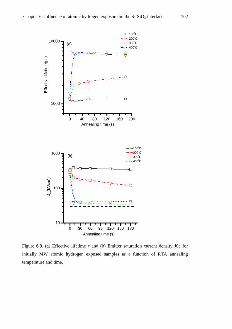
Chapter 6: Influence of atomic hydrogen exposure on the Si-SiO2 interface
102
0 30 60 90 120 150 18010
100
1000
J 0e(f
A/c
m2 )
Annealing time (s)
100oC200oC300oC400oC
(b)
0 40 80 120 160 200
1000
10000E
ffect
ive
lifet
ime(
µs)
Annealing time (s)
100oC 200oC 300oC 400oC
(a)
Figure 6.9. (a) Effective lifetime τ and (b) Emitter saturation current density J0e for
initially MW atomic hydrogen exposed samples as a function of RTA annealing
temperature and time.
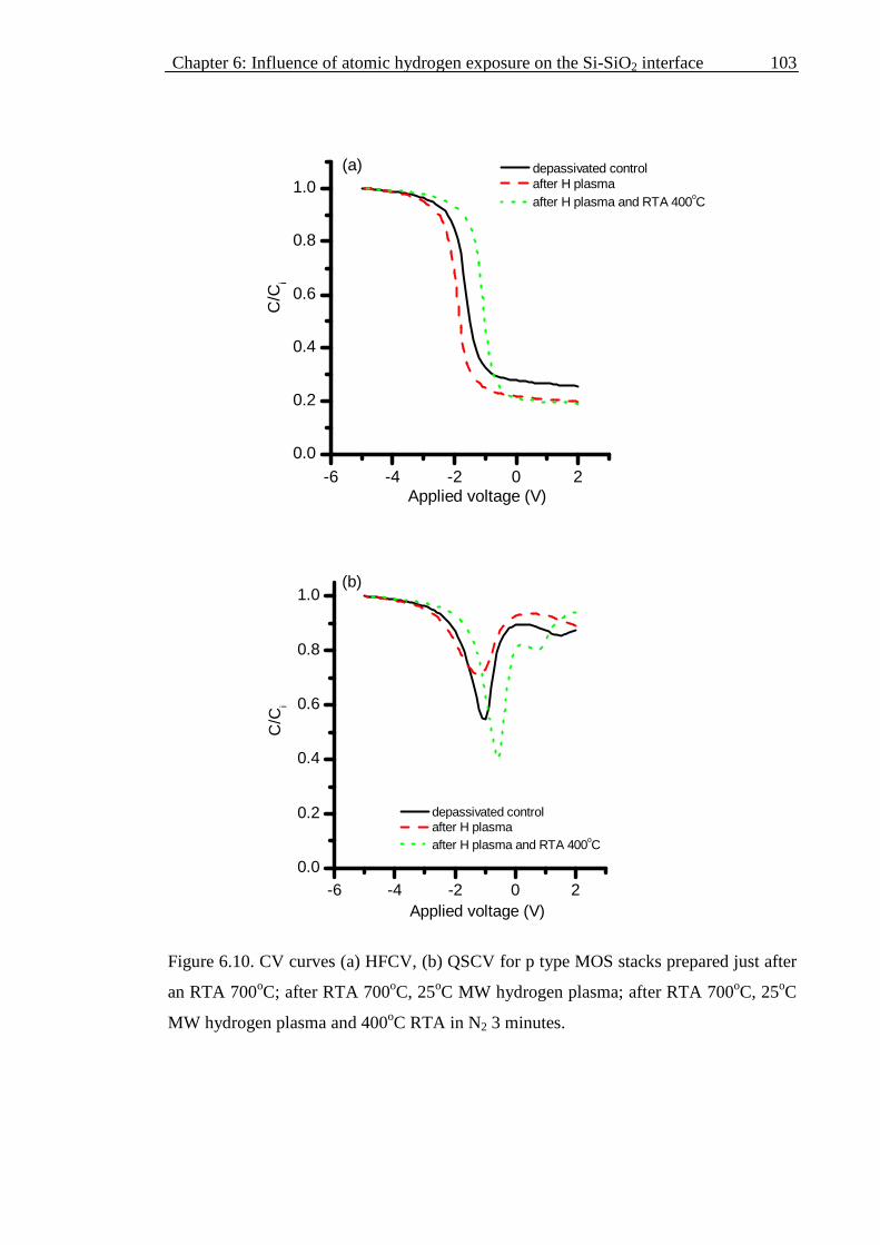
Chapter 6: Influence of atomic hydrogen exposure on the Si-SiO2 interface
103
-6 -4 -2 0 20.0
0.2
0.4
0.6
0.8
1.0
C/C
i
Applied voltage (V)
depassivated control after H plasma after H plasma and RTA 400oC
(b)
-6 -4 -2 0 20.0
0.2
0.4
0.6
0.8
1.0
C/C
i
Applied voltage (V)
depassivated control after H plasma after H plasma and RTA 400oC
(a)
Figure 6.10. CV curves (a) HFCV, (b) QSCV for p type MOS stacks prepared just after
an RTA 700oC; after RTA 700oC, 25oC MW hydrogen plasma; after RTA 700oC, 25oC
MW hydrogen plasma and 400oC RTA in N2 3 minutes.
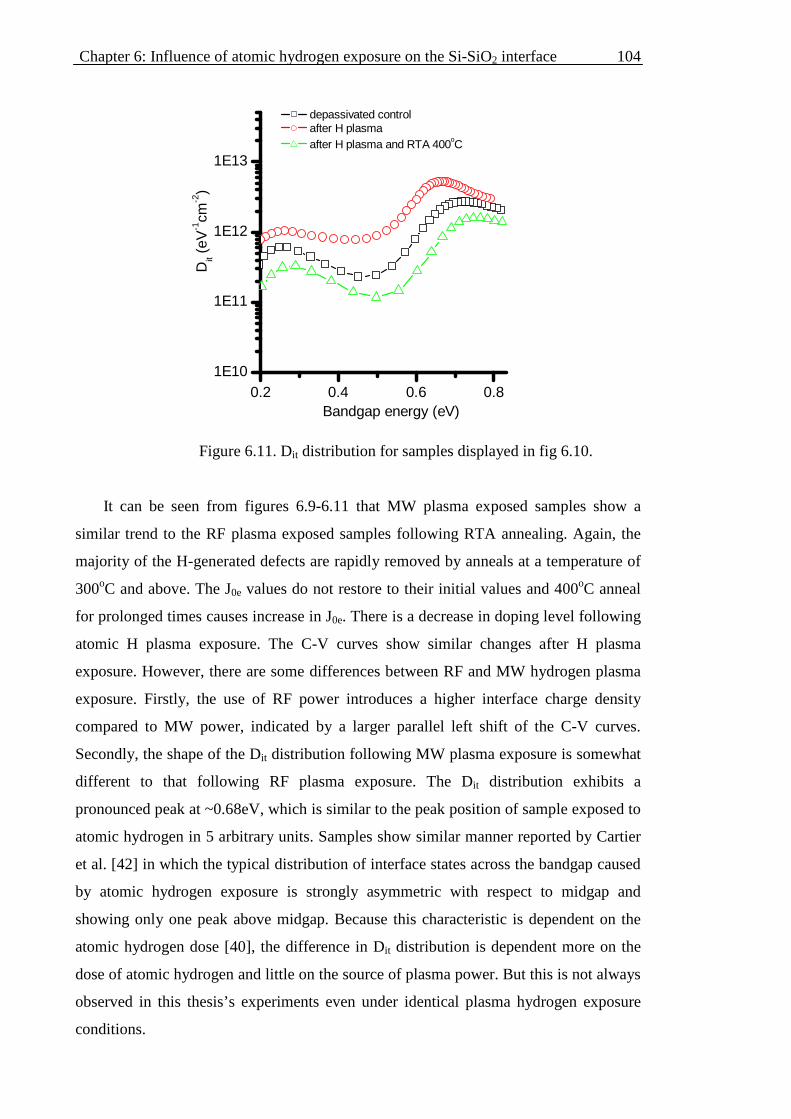
Chapter 6: Influence of atomic hydrogen exposure on the Si-SiO2 interface
104
0.2 0.4 0.6 0.81E10
1E11
1E12
1E13
Dit (
eV-1cm
-2)
Bandgap energy (eV)
depassivated control after H plasma after H plasma and RTA 400oC
Figure 6.11. Dit distribution for samples displayed in fig 6.10.
It can be seen from figures 6.9-6.11 that MW plasma exposed samples show a
similar trend to the RF plasma exposed samples following RTA annealing. Again, the
majority of the H-generated defects are rapidly removed by anneals at a temperature of
300oC and above. The J0e values do not restore to their initial values and 400oC anneal
for prolonged times causes increase in J0e. There is a decrease in doping level following
atomic H plasma exposure. The C-V curves show similar changes after H plasma
exposure. However, there are some differences between RF and MW hydrogen plasma
exposure. Firstly, the use of RF power introduces a higher interface charge density
compared to MW power, indicated by a larger parallel left shift of the C-V curves.
Secondly, the shape of the Dit distribution following MW plasma exposure is somewhat
different to that following RF plasma exposure. The Dit distribution exhibits a
pronounced peak at ~0.68eV, which is similar to the peak position of sample exposed to
atomic hydrogen in 5 arbitrary units. Samples show similar manner reported by Cartier
et al. [42] in which the typical distribution of interface states across the bandgap caused
by atomic hydrogen exposure is strongly asymmetric with respect to midgap and
showing only one peak above midgap. Because this characteristic is dependent on the
atomic hydrogen dose [40], the difference in Dit distribution is dependent more on the
dose of atomic hydrogen and little on the source of plasma power. But this is not always
observed in this thesis’s experiments even under identical plasma hydrogen exposure
conditions.
Chapter 6: Influence of atomic hydrogen exposure on the Si-SiO2 interface
105
6.3.3 Comparison of RTA results at 300oC and 400oC
The results of RTA treatments presented in figs 6.4 and 6.9, for both RF and MW
hydrogen exposed samples, suggest that a 300oC RTA treatment for a short time (less
than 30 seconds) is most effective at removing the thermally unstable defects and
without leading to a loss of hydrogen from H passivated defects (PbH centres). In
comparison, a 400oC RTA treatment results in slightly increased surface recombination,
suggesting a loss of hydrogen from passivated defects. However, this was inconsistent
with the findings of Stesmans, who did not observe a significant increase in [Pb] until
480oC by using conventional tube furnace. This was investigated further.
Figure 6.12 shows the (a) HFCV and (b) QSCV curves for p type MOS stacks
measured after MW hydrogen plasma exposure under standard conditions, and
following an RTA in N2 for 3 minutes at 300oC and 400oC successively. Figure 6.13
shows the corresponding Dit distribution. Three depassivated samples were used. For
comparison, an as oxidized and RTA 700oC de-hydrogenated MOS stack is also shown.
Figure 6.14 shows the J0e values for two oxidised depassivated (100) p-type samples
after different processing steps. The MW plasma conditions are standard. After H
plasma exposure, samples received RTA 300oC 3 minutes in N2 and 400oC 3 minutes in
N2 successively. During RTA, samples were touched directly by thermocouple. The
figure shows the average and error of the two values.

Chapter 6: Influence of atomic hydrogen exposure on the Si-SiO2 interface
106
-6 -4 -2 0 20.0
0.2
0.4
0.6
0.8
1.0C
/Ci
Applied voltage (V)
depassivated control after H plasma after H plasma and 300oC RTA after H plasma and 300oC RTA and 400oC RTA
(a)
-6 -4 -2 0 20.0
0.2
0.4
0.6
0.8
1.0
C/C
i
Applied voltage (V)
depassivated control after H plasma after H plasma and 300oC RTA after H plasma and 300oC RTA and 400oC RTA
(b)
Figure 6.12. (a) HFCV and (b) QSCV curves following different processing steps: after
RTA 700oC 3 minutes; after RTA 700oC 3 minutes and H plasma; after RTA 700oC 3
minutes, H plasma and RTA 300oC, N2, 3 minutes; after RTA 700oC 3 minutes, H
plasma , RTA 300oC, N2, 3 minutes and RTA 400oC 3 minutes.

Chapter 6: Influence of atomic hydrogen exposure on the Si-SiO2 interface
107
0.2 0.4 0.6 0.81E10
1E11
1E12
1E13
Dit (e
V-1cm
-2)
Bandgap energy (eV)
depassivated control after H plasma after H plasma and 300oC RTA after H plasma and 300oC RTA and 400oC RTA
Figure 6.13. Interface defect density (Dit) distribution across the energy gap at the Si-
SiO2 interface subjected to identical situations as those in fig 6.12.
It can be seen from fig 6.12 (a) that after RTA 300oC annealing, the interface
charge density returns to the initial level (about 1.6×1011cm-2), while a subsequent
400oC RTA leads to a further slight decrease to about 1.3×1011cm-2. On the other hand,
from fig 6.12 (b) and 6.13, it can be seen that there is also a decrease in Dit distribution
after a 400oC RTA annealing, and the midgap Dit value decreases from 2.1×10¹¹eV-1cm-
2 to 1.3×10¹¹eV-1cm-2 for 300 and 400oC RTA treatments respectively.

Chapter 6: Influence of atomic hydrogen exposure on the Si-SiO2 interface
108
1 2 3 4 510
100
1000
J 0e(f
A/c
m2 )
Processing steps
Figure 6.14. J0e values for samples following various processing steps. step 1: FGA;
step 2: RTA 700oC in N2 3 minutes; step 3: H plasma exposure; step 4: H plasma
exposure and RTA 300oC in N2 3 minutes; step 5: H plasma exposure, RTA 300oC in N2
3 minutes and successive RTA 400oC in N2 3 minutes.
It can be seen from fig 6.14 that, after H plasma, the J0e values is about 400fA/cm2
and decreases to about 130fA/cm2 after 300oC RTA, then further decreases to around
50fA/cm2 after the 400oC RTA. The lifetime results are consistent to the CV results in
this section; that is, the 400oC RTA results in a further improvement in surface
passivation compared to the 300oC RTA.
It is clear that the results in this section are not consistent with those in fig 6.4 and
6.9, in which the 400oC RTA leads to a slight degradation compared to a 300oC RTA.
The major difference between the two sets of results is the way in which the RTA
treatment was carried out. For the results of the previous section (fig 6.4 and 6.9), a five
inch silicon base plate was used as a substrate to contact the thermocouple rather than a
smaller quarter, in order to minimise the risk of contamination. It appears that this
method resulted in the sample temperature increasing significantly above the measured
temperature. The RTA was done in this section and subsequent experiments in a way in
which the thermocouple directly touched the bottom of the test sample.

Chapter 6: Influence of atomic hydrogen exposure on the Si-SiO2 interface
109
6.4 Effect of atomic hydrogen plasma exposure
parameters on the Si-SiO2 interface
In this section, hydrogenated and de-hydrogenated p-type silicon samples were
exposed to RF or MW plasma atomic hydrogen produced by a PECVD reactor,
followed by RTA and FGA treatments. The effects of atomic H plasma power, pressure
and time on Si-SiO2 interface passivation were studied.
6.4.1 Influence of hydrogen plasma exposure power on Si-
SiO2 interface defect distribution
6.4.1.1 RF power
The section aims to investigate the effect of RF power on the Si-SiO2 interface
properties following H exposure. A higher power level of the excitation source will lead
to a higher degree of dissociation of the process gases. For PECVD film depositions,
this usually results in a better uniformity of the deposited layers and an increase in
deposition rate. On the other hand, a higher power level will also produce a greater
density of energetic ions which can produce damage at the wafer surface and thus, a
degradation of the surface properties [120].
Figure 6.15 exhibits (a) C-V curves and (b) corresponding Dit distribution for
initially passivated Si-SiO2 stacks after RF hydrogen plasma exposure with RF power
ranging from 50 to 300W and under otherwise standard conditions. Table 6.2
summarizes the flat band voltage, interface charge density, and midgap interface defect
density for these samples. For comparison, the corresponding curve for an as oxidized
and forming gas annealed MOS stack is also shown.

Chapter 6: Influence of atomic hydrogen exposure on the Si-SiO2 interface
110
0.2 0.4 0.6 0.8
1E9
1E10
1E11
1E12
1E13
1E14
Dit(
eV-1cm
-2)
Bandgap energy (eV)
150 W 300 W passivated control
(b)
-25 -20 -15 -10 -5 00.0
0.2
0.4
0.6
0.8
1.0
C/C
i
Applied voltage (V)
150W HFCV 150W QSCF 300W HFCV 300W QSCF passivated control HFCV passivated control QSCV
(a)
Figure 6.15. (a) C-V curves and (b) corresponding Dit distribution for initially
passivated Si-SiO2 stacks after RF hydrogen plasma exposure at an RF power ranging
from 150 to 300W and otherwise standard conditions.

Chapter 6: Influence of atomic hydrogen exposure on the Si-SiO2 interface
111
Table 6.2. Flatband voltage(V), interface charge density(x1011cm-2), and midgap
surface defect density(x1010eV-1cm-2 ) after various RF power H plasma exposure.
As can be seen from fig 6.15 (a), there is a big shift along the voltage axis and a rise
of the minimum quasistatic capacitance for 150W and 300W samples, which means,
with increasing RF exposure power, there is a corresponding significant increase in
interface charge and defect density to the Si-SiO2 interface. Fig 6.15 (b) also presents
the evidence that a plasma power as low as 150W can generate a high density of
interface defects. Again, an appreciable decrease in doping level following atomic
hydrogen plasma exposure can be observed in fig 6.15 (a). For an exposure power
between 150-300W there does not seem to be a significant difference in Si-SiO2
interface passivation, although a slightly higher charge and defect density is produced at
300W.
6.4.1.2 MW power
Figure 6.16 shows J0e values for initially passivated Si-SiO2 stacks after H plasma
exposure at a MW power ranging from 200 to 1200W under otherwise standard
conditions, as well as the J0e values for the same samples after a subsequent RTA at
400oC for 3 minutes in N2 and an FGA at 400oC for 30 minutes. Figure 6.17 shows the
results for depassivated samples subjected to identical H plasma exposure and thermal
anneal treatments. The J0e values at the first step come from samples that did not receive
any plasma exposure. Figure 6.18 shows (a) HFCV and (b) QSCV curves for initially
passivated p type MOS stacks measured after different processing steps. Samples were
subjected to MW hydrogen plasma exposure at 1200W and under otherwise standard
conditions. Figure 6.19 shows corresponding Dit distribution, four passivated samples
were used.
Vfb Q Ditm RF 300W -18 66 680 RF 150W -15 52 520 Passivated control
-1 0.66 0.39

Chapter 6: Influence of atomic hydrogen exposure on the Si-SiO2 interface
112
1 2 3 4 510
100
1000
J 0e (
fA/c
m2 )
Processing steps
MW 200 W MW 800 W MW 1200 W
depassivated samples
1 2 3 410
100
1000
J 0e (
fA/c
m2 )
Processing steps
MW 200 W MW 250 W MW 400 W MW 800 W MW 1200 W
passivated samples
Figure 6.16. J0e values for passivated samples following different treatments. Step 1:
FGA; step 2: H plasma exposure; step 3: RTA 400oC 3 minutes in N2; step 4: FGA
400oC 30 minutes.
Figure 6.17. J0e values for depassivated samples following different treatments. Step 1:
FGA; step 2: RTA 700oC 3 minutes in N2; step 3: H plasma exposure; step 4: RTA
400oC 3 minutes in N2; step 5: FGA 400oC 30 minutes.

Chapter 6: Influence of atomic hydrogen exposure on the Si-SiO2 interface
113
-10 -8 -6 -4 -2 0 2 40.0
0.2
0.4
0.6
0.8
1.0
C/C
i
Applied voltage (V)
passivated control after H plasma after H plasma and RTA 400oC after H plasma and RTA 400oC and FGA 400oC
(a)
-10 -8 -6 -4 -2 0 2 4
0.2
0.4
0.6
0.8
1.0
C/C
i
Applied voltage (V)
passivated control after H plasma after H plasma and RTA 400oC after H plasma and RTA 400oC and FGA 400oC
(b)
Figure 6.18. CV curves (a) HFCV, (b) QSCV for p type MOS stacks prepared just after
an FGA; after FGA and 1200W hydrogen plasma exposure; after FGA, 1200W
hydrogen plasma exposure and 400oC RTA 3 minutes; after FGA, 1200W hydrogen
plasma exposure, 400oC RTA 3 minutes and FGA.

Chapter 6: Influence of atomic hydrogen exposure on the Si-SiO2 interface
114
0.2 0.4 0.6 0.8
1E9
1E10
1E11
1E12
1E13
Dit (
eV-1cm
-2)
Bandgap energy (eV)
passivated control after H plasma after H plasma and RTA 400oC after H plasma and RTA 400oC and FGA 400oC
Figure 6.19. Dit distribution across the energy gap for initially passivated samples
following identical processing steps as in fig 6.18.
It can be seen from fig 6.16 and 6.17 that there is a permanent degradation of the
interface with increasing MW power, especially for the 1200W exposed samples.
Although the subsequent 400oC RTA and FGA treatments can significantly improve the
surface passivation, the final J0e values (after second FGA) are much higher than initial
values, indicating that a high plasma power generates defects which are not removed by
subsequent anneals at 400oC. These defects are presumed to have a different origin to
the atomic hydrogen induced defects, although their exact origin is not clear. At a power
level of 200-400W, the J0e values come back to the initial level (before plasma) after a
400oC FGA, indicating that the additional defects created during H plasma exposure in
this power range can be removed at low temperatures (≤400oC). At intermediate power
levels between 400 and 1200W, additional defects may also be generated, as can be
seen from the results for 800W MW power. The chief conclusion is that even a remote,
high frequency plasma source can result in the introduction of plasma-generated
interface defects, and that great care must be taken in the choice of the operating
parameters.
It can be seen from figs 6.18 and 6.19 that the RTA treatment has resulted in only a
small reduction in interface defect density; this reduction is much smaller than is usually
Chapter 6: Influence of atomic hydrogen exposure on the Si-SiO2 interface
115
observed for samples exposed at lower plasma powers. However, following an FGA the
interface defect density is almost the same as the initial defect density prior to plasma
exposure. Given the fact that J0e following an FGA is still significantly higher than the
initial J0e, this may indicate that defects in the emitter (that is, in the near-surface region
of the silicon) are perhaps the most likely explanation for this. It is also can be seen in
fig 6.18 (a) that the voltage shift, indicating positive charge density, is much smaller
compared with RF hydrogen plasma exposed sample. This means there seems to be a
significant difference in the effect of the two different plasmas, and the high positive
charge density observed for RF plasmas (and also by Cartier et al.) [119] may not be a
fundamental property of the atomic hydrogen exposure. Again, there is a reduction in
minimum capacitance after MW hydrogen plasma exposure and the explanation for fig
6.5 (a) for RF plasma can be applied here. It should be noted that although high plasma
power will introduce defects in the emitter near the surface region of the silicon, the Dit
level is not much higher than that following lower power exposure. This may be due to
experimental error - slightly different exposure conditions every time a sample is
exposed in the chamber (i.e. the different H plasma density and uniformity). Further
work is worth to confirm this.
6.4.2 Influence of hydrogen plasma exposure time on Si-SiO2
interface defect distribution
Usually, the atomic hydrogen dose during plasma exposure is proportional to
exposure time. In this section, the effect of hydrogen exposure time on passivation of
Si-SiO2 defects has been investigated.
6.4.2.1 RF power plasma hydrogen exposure
Figure 6.20 shows the (a) HFCV and (b) QSCV curves for two oxidised passivated
samples following RF hydrogen plasma exposure for 5 and 20 minutes, respectively,
with otherwise standard process parameters. Figure 6.21 shows the corresponding Dit
distribution. Table 6.3 summarizes the flat band voltage (Vfb), interface charge density
(V), and defect density at mid gap (Ditm) following the same process steps. Figure 6.22
shows (a) the effective lifetime and (b) the corresponding J0e values for oxidised
passivated samples following different processing steps. Figure 6.23 shows the
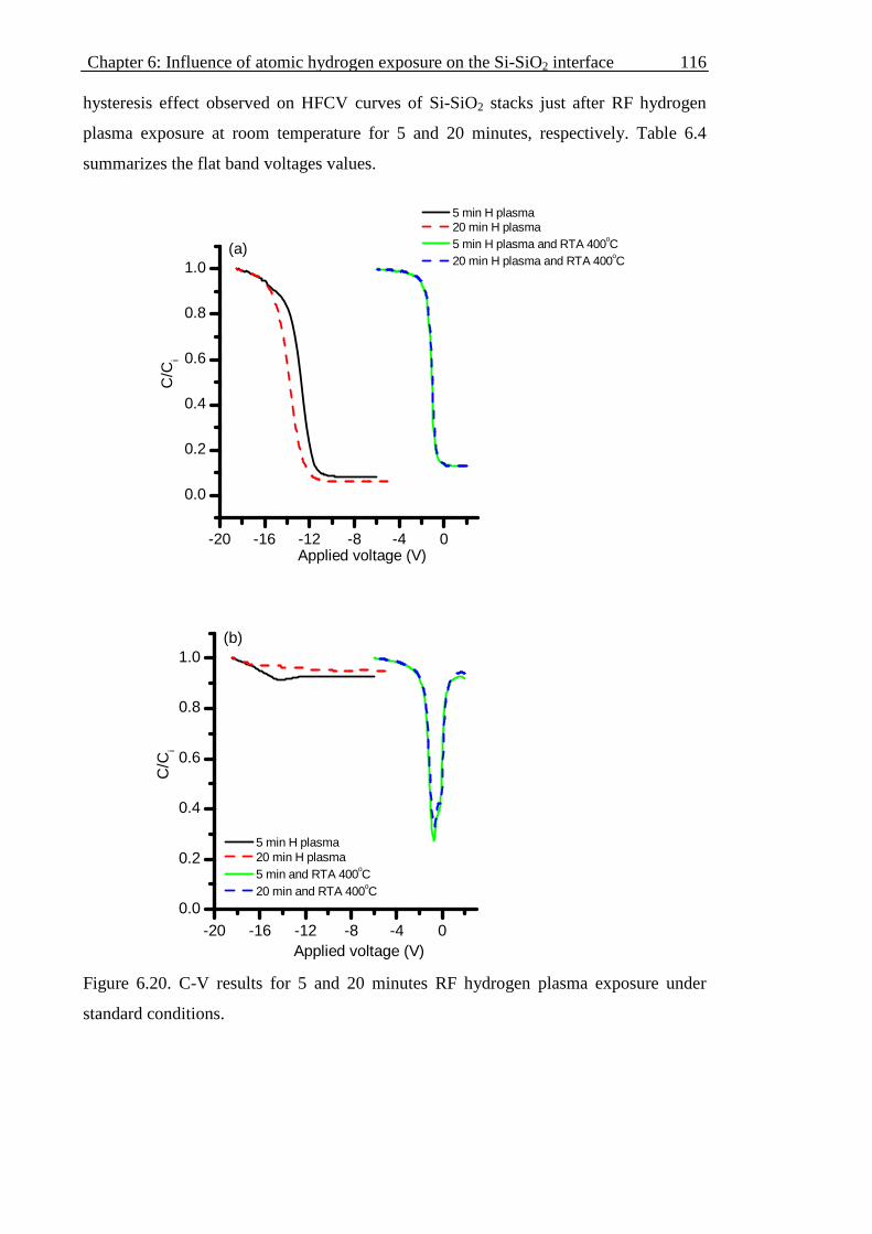
Chapter 6: Influence of atomic hydrogen exposure on the Si-SiO2 interface
116
-20 -16 -12 -8 -4 0
0.0
0.2
0.4
0.6
0.8
1.0
C/C
i
Applied voltage (V)
5 min H plasma 20 min H plasma 5 min H plasma and RTA 400oC 20 min H plasma and RTA 400oC
(a)
-20 -16 -12 -8 -4 00.0
0.2
0.4
0.6
0.8
1.0
C/C
i
Applied voltage (V)
5 min H plasma 20 min H plasma 5 min and RTA 400oC 20 min and RTA 400oC
(b)
hysteresis effect observed on HFCV curves of Si-SiO2 stacks just after RF hydrogen
plasma exposure at room temperature for 5 and 20 minutes, respectively. Table 6.4
summarizes the flat band voltages values.
Figure 6.20. C-V results for 5 and 20 minutes RF hydrogen plasma exposure under
standard conditions.

Chapter 6: Influence of atomic hydrogen exposure on the Si-SiO2 interface
117
0.4 0.6 0.8
1E9
1E10
1E11
1E12
1E13
1E14
Dit (
eV-1cm
-2)
Bandgap energy (eV)
5 min H plasma 20 min H plasma 5 min H plasma and RTA 400oC 20 min H plasma and RTA 400oC
Figure 6.21. Dit distribution for 5 and 20 minutes RF hydrogen plasma exposure under
standard conditions.
Table 6.3. Flatband voltage Vfb(V), interface charge density Q(x1011cm-2), and midgap
surface defect density Ditm(x1011eV-1cm-2 )for samples following various processing
treatments.
Vfb Q Ditm 5 minutes H plasma -12.4 42 44 20 minutes H plasma -13.3 43 62 5 minutes H plasma and RTA
-1.1 1.1 1.1
20 minutes H plasma and RTA
-1.0 1.0 1.7

Chapter 6: Influence of atomic hydrogen exposure on the Si-SiO2 interface
118
1 2 3 4100
1000
Effe
ctiv
e lif
etim
e (µ
s)
Processing steps
RF 5 min H plasma RF 20 min H plasma
(a)
1 2 3 4
100J 0e(f
A/c
m2 )
Processing steps
RF 5 min H plasma RF 20 min H plasma
(b)
-20 -16 -12 -8 -4
0
50
100
150
200
250
300
20 min accumulation to inversionC
apac
itanc
e (p
F)
Applied voltage (V)
5 min inversion to accumulation5 min accumulation to inversion
20 min inversion to accumulation
HFCV
Figure 6.22. (a) Effective lifetime (b) J0e values for 5 and 20 minutes RF hydrogen
exposure samples following various processing steps. Step1: after FGA, Step 2: after
RF H plasma exposure, Step 3: after RTA 400oC in N2 3 minutes, Step 4: after FGA.
Figure 6.23. HFCV curves for 5 and 20 minutes RF hydrogen plasma exposure under
standard conditions.
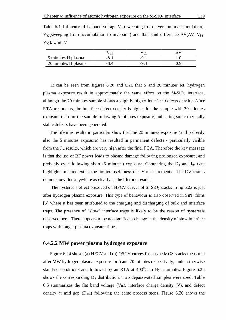
Chapter 6: Influence of atomic hydrogen exposure on the Si-SiO2 interface
119
Table 6.4. Influence of flatband voltage Vb1(sweeping from inversion to accumulation),
Vb2(sweeping from accumulation to inversion) and flat band difference ∆V(∆V=Vb1-
Vb2). Unit: V
It can be seen from figures 6.20 and 6.21 that 5 and 20 minutes RF hydrogen
plasma exposure result in approximately the same effect on the Si-SiO2 interface,
although the 20 minutes sample shows a slightly higher interface defects density. After
RTA treatments, the interface defect density is higher for the sample with 20 minutes
exposure than for the sample following 5 minutes exposure, indicating some thermally
stable defects have been generated.
The lifetime results in particular show that the 20 minutes exposure (and probably
also the 5 minutes exposure) has resulted in permanent defects - particularly visible
from the J0e results, which are very high after the final FGA. Therefore the key message
is that the use of RF power leads to plasma damage following prolonged exposure, and
probably even following short (5 minutes) exposure. Comparing the Dit and J0e data
highlights to some extent the limited usefulness of CV measurements - The CV results
do not show this anywhere as clearly as the lifetime results.
The hysteresis effect observed on HFCV curves of Si-SiO2 stacks in fig 6.23 is just
after hydrogen plasma exposure. This type of behaviour is also observed in SiNx films
[5] where it has been attributed to the charging and discharging of bulk and interface
traps. The presence of “slow” interface traps is likely to be the reason of hysteresis
observed here. There appears to be no significant change in the density of slow interface
traps with longer plasma exposure time.
6.4.2.2 MW power plasma hydrogen exposure
Figure 6.24 shows (a) HFCV and (b) QSCV curves for p type MOS stacks measured
after MW hydrogen plasma exposure for 5 and 20 minutes respectively, under otherwise
standard conditions and followed by an RTA at 400oC in N2 3 minutes. Figure 6.25
shows the corresponding Dit distribution. Two depassivated samples were used. Table
6.5 summarizes the flat band voltage (Vfb), interface charge density (V), and defect
density at mid gap (Ditm) following the same process steps. Figure 6.26 shows the
Vb1 Vb2 ∆V 5 minutes H plasma -8.1 -9.1 1.0 20 minutes H plasma -8.4 -9.3 0.9
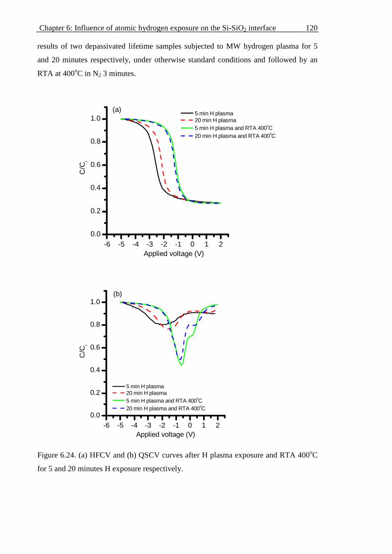
Chapter 6: Influence of atomic hydrogen exposure on the Si-SiO2 interface
120
-6 -5 -4 -3 -2 -1 0 1 20.0
0.2
0.4
0.6
0.8
1.0
C/C
i
Applied voltage (V)
5 min H plasma 20 min H plasma 5 min H plasma and RTA 400oC 20 min H plasma and RTA 400oC
(a)
-6 -5 -4 -3 -2 -1 0 1 20.0
0.2
0.4
0.6
0.8
1.0
C/C
i
Applied voltage (V)
5 min H plasma 20 min H plasma 5 min H plasma and RTA 400oC 20 min H plasma and RTA 400oC
(b)
results of two depassivated lifetime samples subjected to MW hydrogen plasma for 5
and 20 minutes respectively, under otherwise standard conditions and followed by an
RTA at 400oC in N2 3 minutes.
Figure 6.24. (a) HFCV and (b) QSCV curves after H plasma exposure and RTA 400oC
for 5 and 20 minutes H exposure respectively.

Chapter 6: Influence of atomic hydrogen exposure on the Si-SiO2 interface
121
0.2 0.3 0.4 0.5 0.6 0.7 0.81E10
1E11
1E12
1E13
Dit(e
V-1cm
-2)
Bandgap energy (eV)
5 min H plasma 20 min H plasma 5 min H plasma and RTA 400oC 20 min H plasma and RTA 400oC
Figure 6.25. Dit distribution across the energy gap for initially depassivated samples for
5 and 20 minutes H exposure respectively.
Table 6.5. Flatband voltage Vfb(V), interface charge density Q(x1011cm-2), and midgap
surface defect density Ditm(x1011eV-1cm-2 )for samples following various processing
treatments.
Vfb Q Ditm 5 minutes H plasma -2.6 5.6 17 20 minutes H plasma -2.2 4.3 17 5 minutes H plasma and RTA
-1.2 1.3 1.3
20 minutes H plasma and RTA
-1.2 1.5 2.0

Chapter 6: Influence of atomic hydrogen exposure on the Si-SiO2 interface
122
1 2 31000
2000
3000
4000
5000
Effe
ctiv
e lif
etim
e (µ
s)
Processing steps
MW 5 min H plasma MW 20 min H plasma
(a)
1 2 3
100
1000
J 0e(f
A/c
m2 )
Processing steps
MW 5 min H plasma MW 20 min H plasma
(b)
Figure 6.26. Comparison of the effective lifetime and J0e values between 5 and 20
minutes MW hydrogen plasma exposed samples following different steps. Step1: RTA
700oC, Step 2: MW hydrogen plasma 5 and 20 minutes respectively, Step 3: RTA
400oC in N2 3 minutes.
In contrast to the last section, depassivated samples were used in this section. CV
results show that, after 5 and 20 minutes H plasma exposure, the midgap Dit values are
nearly identical for the two samples, suggesting that there is little additional defects
generation. However there appears to be a higher defect density above midgap energy
level for 20 minutes sample. Following subsequent RTA, Dit value is higher for 20
minute sample, suggesting that there is some thermally stable defects generation. In
comparison to the samples following RF exposure in the previous subsection, the Dit
value is slightly higher following RTA.
J0e results are similar to CV results. The results following the RTA suggest that
long time exposure can still result in some permanent interface damage, since J0e value
following 20 minutes exposure is higher than that after 5 min exposure. This can clearly
not be due to PbH passivation-depassivation.
6.4.3 Influence of hydrogen plasma exposure pressure on Si-
SiO2 interface defect distribution

Chapter 6: Influence of atomic hydrogen exposure on the Si-SiO2 interface
123
0 100 200 300 400
10
100
1000
J 0e(f
A/c
m2 )
Plasma power (W)
0.2 mbar H plasma 0.2 mbar H plasma and 400oC RTA 0.67 mbar H plasma 0.67 mbar H plasma and 400oC RTA
(b)
passivated sample
0 100 200 300 40010
100
1000
J 0e(f
A/c
m2 )
Plasma power (W)
0.2 mbar H plasma 0.2mbar H plasma and 400oC RTA 0.67 mbar H plasma 0.67 mbar H plasma and 400oC RTA
(a)
depassivated sample
Figure 6.27 shows J0e values for initially (a) depassivated and (b) passivated Si-
SiO2 stacks after 5 minutes H plasma exposure at room temperature, at a MW power
ranging from 200 to 400W and a pressure 0.2 and 0.67mbar respectively. This was
followed by an RTA at 400oC for 3 minutes in N2. J0e at zero exposure time come from
samples that did not receive any plasma exposure.
Figure 6.27. Comparison J0e values at 0.2 and 0.67 mbar for H plasma exposed and
subsequent RTA 400oC N2 3 minutes for (a) depassivated and (b) passivated samples.

Chapter 6: Influence of atomic hydrogen exposure on the Si-SiO2 interface
124
It can be seen from figure 6.27 that more interface damage occurs with higher
pressure at a MW power in the range 200 to 400W. After a 400oC RTA (removing
thermally unstable defects), no significant difference is observed between the 0.2mbar
and 0.67mbar exposure. This trend was observed for both passivated and depassivated
samples. The results indicate that higher pressure has the effect of accelerating the rate
of generation of defects at lower pressure. In other words, the density of atomic
hydrogen in the plasma is a function of both the pressure and the MW power. For
sufficiently high plasma power (400W), for an exposure time of 5 minutes saturation in
J0e (and presumably Dit) is observed for both pressures. In addition, the passivation of
thermally stable interface defects appears to have reached steady state after 5 minutes at
0.2mbar, while the density of unstable defects has not yet reached steady state.
6.4.4 Optimization of the atomic hydrogen plasma exposure
parameters
The section aims to achieve plasma operating conditions which, on the one hand,
can avoid plasma damage (i.e. introduction of defects which do not appear to be due to
the action of atomic H itself but more likely the result of the bombardment of the
surface with energetic particles), and on the other hand ideally, result in a sufficient H
flux to result in steady state passivation of existing interface defects (Pb) and saturation
of atomic H induced defects.
Results in previous sections suggest that both RF and MW can result in damage if
exposure time is too long or power is too high. J0e results in particular indicate that RF
power results in more damage than MW power. Even 5 minutes exposure can result in
introduction of permanent defects.
Overall conclusion is that it is best to use MW plasma with low power(200W), and
minimise exposure time(5 minutes). Plasma conditions are a compromise - from the
results of the section on influence of process pressure it is apparent that 5 minutes at
0.2mbar is not enough to result in saturation of thermally unstable defects.
6.5 Effect of MW hydrogen plasma exposure and
following thermal anneal on the Si-SiO2 interface

Chapter 6: Influence of atomic hydrogen exposure on the Si-SiO2 interface
125
-12 -10 -8 -6 -4 -2 0 2
0.2
0.4
0.6
0.8
1.0
C/C
i
Applied voltage (V)
before MW H plasma HFCV before MW H plasma QSCV after MW H plasma HFCV after MW H plasma QSCV
In our PECVD system, the MW hydrogen plasma is produced by using the so-called
remote PECVD method, in which the Si wafers are located outside the plasma region,
allowing the hydrogen plasma exposure with virtually no surface damage of the samples
[121]. The effect of atomic hydrogen on the Si-SiO2 interface by using this technique is
to be discussed below.
6.5.1 Effect of MW hydrogen plasma exposure and following
thermal anneal on the Si-SiO2 interface
This section summarises the results of atomic H exposure on the (100) thermally
oxidised Si-SiO2 interface, using the conditions that have been determined to be optimal
from the experimental results presented in previous sections.
Figure 6.28 shows the CV curves for p type MOS stacks measured before and after
MW hydrogen plasma exposure under standard conditions. Figure 6.29 shows the
corresponding Dit distribution. Two passivated samples were used. Figures 6.30 and
6.31 show the results of depassivated samples received MW H plasma exposure under
identical conditions.
Figure 6.28. C-V curves before and after MW hydrogen plasma exposure under
standard conditions for initially passivated samples.

Chapter 6: Influence of atomic hydrogen exposure on the Si-SiO2 interface
126
0.2 0.4 0.6 0.8
1E9
1E10
1E11
1E12
1E13
1E14D
it(eV
-1cm
-2)
Bandgap energy (eV)
before MW H plasma after MW H plasma
passivated sample
-12 -10 -8 -6 -4 -2 0 20.0
0.2
0.4
0.6
0.8
1.0
C/C
i
Applied voltage (V)
before H plasma HFCV before H plasma QSCV after H plasma HFCV after H plasma QSCV
depassivated sample
Figure 6.29. Dit distribution across the energy gap at the Si-SiO2 interface for samples
displayed in fig 6.28.
Figure 6.30. C-V curves before and after MW hydrogen plasma exposure under
standard condition for initially depassivated samples.
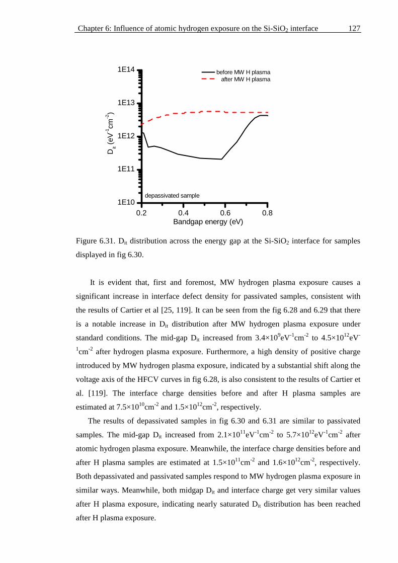
Chapter 6: Influence of atomic hydrogen exposure on the Si-SiO2 interface
127
0.2 0.4 0.6 0.81E10
1E11
1E12
1E13
1E14
Dit (
eV-1cm
-2)
Bandgap energy (eV)
before MW H plasma after MW H plasma
depassivated sample
Figure 6.31. Dit distribution across the energy gap at the Si-SiO2 interface for samples
displayed in fig 6.30.
It is evident that, first and foremost, MW hydrogen plasma exposure causes a
significant increase in interface defect density for passivated samples, consistent with
the results of Cartier et al [25, 119]. It can be seen from the fig 6.28 and 6.29 that there
is a notable increase in Dit distribution after MW hydrogen plasma exposure under
standard conditions. The mid-gap Dit increased from 3.4×10⁹eV-1cm-2 to 4.5×10¹²eV-
1cm-2 after hydrogen plasma exposure. Furthermore, a high density of positive charge
introduced by MW hydrogen plasma exposure, indicated by a substantial shift along the
voltage axis of the HFCV curves in fig 6.28, is also consistent to the results of Cartier et
al. [119]. The interface charge densities before and after H plasma samples are
estimated at 7.5×1010cm-2 and 1.5×1012cm-2, respectively.
The results of depassivated samples in fig 6.30 and 6.31 are similar to passivated
samples. The mid-gap Dit increased from 2.1×10¹¹eV-1cm-2 to 5.7×10¹²eV-1cm-2 after
atomic hydrogen plasma exposure. Meanwhile, the interface charge densities before and
after H plasma samples are estimated at 1.5×1011cm-2 and 1.6×1012cm-2, respectively.
Both depassivated and passivated samples respond to MW hydrogen plasma exposure in
similar ways. Meanwhile, both midgap Dit and interface charge get very similar values
after H plasma exposure, indicating nearly saturated Dit distribution has been reached
after H plasma exposure.

Chapter 6: Influence of atomic hydrogen exposure on the Si-SiO2 interface
128
To further determine the effect of atomic hydrogen produced by MW on interface
recombination, two initially passivated samples for lifetime measurements were
exposed to a H plasma under standard conditions. J0e values of these samples increased
from 28fA/cm2 to 260±20fA/cm2 following plasma exposure. It should be noted that J0e
is influenced by interface charge as well as by changes in the interface defect density.
The increase in positive charge following H plasma exposure would, in the absence of
changes to the interface defect density or properties, be expected to result in a small
decrease in J0e, based on the calculated decrease in the surface minority carrier
concentration by this amount. The J0e results are in good qualitative agreement with the
C-V results: a large increase in the interface defect density causes a large increase in
surface recombination, indicating that the additional defects introduced by atomic H act
as efficient carrier recombination centres. However, the increase in Dit is substantially
larger than the increase in J0e. This is probably the result of different capture cross
sections of the H-introduced defects compared to the existing interface defects (Pbx
centres).
Following H plasma exposure, selected samples received RTA and FGA annealing
successively. Figure 6.32 shows (a) HFCV and (b) QSCV curves for p type MOS stacks
measured following various processing steps. Atomic hydrogen plasma exposure was
under standard conditions. Figure 6.33 shows the corresponding Dit distribution. Four
depassivated samples were used. For comparison, an as oxidized and RTA 700oC de-
hydrogenated MOS stack is also shown. Figure 6.34 shows the effective lifetime values
for oxidised, passivated and undiffused sample following different processing steps.
MW hydrogen plasma conditions are standard.

Chapter 6: Influence of atomic hydrogen exposure on the Si-SiO2 interface
129
-6 -4 -2 0 2
0.2
0.4
0.6
0.8
1.0
C/C
i
Applied voltage (V)
depassivated control after H plasma after H plasma and RTA 400oC after H plasma and RTA 400oC and FGA 400oC
(a)
-6 -4 -2 0 20.0
0.2
0.4
0.6
0.8
1.0
C/C
i
Applied voltage (V)
depassivated control after H plasma after H plasma and RTA 400oC after H plasma and RTA 400oC and FGA 400oC(b)
Figure 6.32. (a) HFCV and (b) QSCV curves following different processing steps: after
RTA 700oC 3 minutes; after RTA 700oC 3 minutes and H plasma; after RTA 700oC 3
minutes, H plasma, and RTA 400oC, N2, 3minutes; after RTA 700oC 3 minutes, H
plasma and RTA 400oC, N2, 3 minutes and FGA.

Chapter 6: Influence of atomic hydrogen exposure on the Si-SiO2 interface
130
1 2 3 4100
1000
10000
Effe
ctiv
e lif
etim
e (µ
s)
Processing steps
undiffused sample
0.2 0.4 0.6 0.81E9
1E10
1E11
1E12
1E13
Dit (
eV-1cm
-2)
Bandgap energy (eV)
depassivated control after H plasma after H plasma and RTA 400oC after H plasma and RTA 400oC and FGA 400oC
Figure 6.33. Interface defect density (Dit) distribution across the energy gap at the Si-
SiO2 interface following the identical processing steps in fig 6.32.
Figure 6.34. Effective lifetime values for undiffused samples following various
processing steps. Step 1: FGA; step 2: H plasma exposure; step 3: RTA 400oC 3
minutes in N2; step 4: FGA.

Chapter 6: Influence of atomic hydrogen exposure on the Si-SiO2 interface
131
The CV results show that firstly, the mid-gap Dit values are 4.5×10¹¹eV-1cm-2 to
1.6×10¹²eV-1cm-2 before and after H plasma exposure. Secondly, H plasma exposure
can also improve the passivation of Si-SiO2 interface, indicated by a decrease of
minimum capacitance in quasi static CV curves in fig 6.32 (b) and a decrease of Dit
distribution in fig 6.33 for the curves after H plasma and RTA 400oC compared to
control sample. Actually, the mid-gap Dit values are 1.6×10¹²eV-1cm-2 to 1.6×10¹¹eV-
1cm-2 before and after RTA 400oC annealing. Thirdly, after FGA treatment, the mid-gap
Dit decreases to 1.8×10¹⁰eV-1cm-2, indicating molecular H2 is more efficient at
passivating interface defects than atomic hydrogen.
It can be seen from fig 6.34 that undiffused sample displays a similar trend to
diffused sample as well. A substantial decrease in effective lifetime can be observed
following H plasma exposure, and with a significant increase following a 400oC RTA
and a further increase following FGA 400oC treatment. It should be noted that the
recovery extent following thermal annealing, either RTA or FGA, is lower than those
diffused samples since undiffused samples are more sensitive to surface passivation. In
a nutshell, diffused and undiffused surfaces respond to atomic hydrogen treatments in
similar ways.
The above results, firstly, indicate that atomic hydrogen can result in good Si
surface passivation, indicating a re-introduction of atomic hydrogen to the Si-SiO2
interface. Furthermore, after FGA the mid-gap Dit value is low and close to passivated
level, suggesting little or no introduction of additional defects during hydrogen plasma
exposure. It should be noted that the increase in Dit (and red -o- line in fig 6.33) after
atomic hydrogen plasma exposure for depassivated sample should be a competition
result of introduction of thermally unstable defects and passivation effect of Pbx centres,
and the former is more stronger in that case. Secondly, it is clear from the results in fig
6.34 that undiffused sample responds to atomic hydrogen exposure in a similar way to
diffused sample.
6.5.2 Influence of hydrogen plasma exposure temperature on
Si-SiO2 interface passivation
Figure 6.35 shows the effect of sample temperature during MW hydrogen plasma
exposure under standard conditions. Seven passivated samples were used.

Chapter 6: Influence of atomic hydrogen exposure on the Si-SiO2 interface
132
1 2 3 410
100
1000
J 0e (
fA/c
m2 )
Processing steps
25oC 100oC 200oC 300oC 400oC 500oC 600oC
Figure 6.35. Variation of J0e for initially passivated samples following various
processing steps, for different sample temperatures during H plasma exposure. step 1:
FGA; step 2: H plasma exposure; step 3: RTA 400oC 3 minutes; step 4: FGA.
As can be seen from the results in fig 6.35, sample temperature during plasma
exposure results in significant differences in J0e just after H exposure, due to the fact
that defect generation and annealing occur simultaneously, with the rate of annealing
increasing with increasing temperature. However, temperature has no discernible effect
on J0e results after RTA or FGA. In particular, at all sample temperatures in the range
25-600oC, the degree of surface passivation following H plasma treatment (and after
subsequent thermal treatments) is equal to or slightly worse than that following
passivation by H2 using an FGA. This suggests that the hydrogenation of Pb centres with
atomic H is no more efficient (and probably somewhat less efficient) than the
hydrogenation with H2 at the optimal temperature.
The very weak temperature dependence of Pbx defect passivation observed in our
experiments was predicted by Cartier et al [40]. Atomic hydrogen plasma exposure of
the Si-SiO2 interface results in competition reactions between passivation and
depassivation of Pbx centres. Both of these reactions occur with essentially no energy
barrier, so that the fraction of Pbx centres is determined by the reaction cross sections σ1
and σ2 of passivation and depassivation reactions:

Chapter 6: Influence of atomic hydrogen exposure on the Si-SiO2 interface
133
1
2max ][][
][
σσ=
− sbxbx
sbx
PP
P (6-1)
independent of the initial (unpassivated) Pb centre density Pbx, and only weakly
dependent on temperature. Here, [Pbx]s is the steady-state value of the unpassivated Pbx
centre density and [Pbx]max is the total Pbx centre density.
The different Pb centres that have been identified (Pb at the (111) Si-SiO2 interface,
Pb0 and Pb1 at the (100) interface) appear to have quite different reaction cross sections
[39, 40], leading to different degrees of steady-state passivation.
This situation can be contrasted with the accepted theory concerning the action of
molecular hydrogen, which can also passivate and depassivate Pbx centre simultaneously.
In contrast to atomic hydrogen exposure, both these processes have a significant energy
barrier, resulting in a strong temperature dependence of the passivation. Note that the
reaction of H2 with Pbx centres creates atomic hydrogen, so that in principle, atomic
hydrogen reactions will take place as well. However, these reactions are usually
neglected and are assumed not to play a significant role due to the much lower densities
of atomic compared to molecular hydrogen; an assumption for which there is some
experimental support [23].
6.6 Effect of hydrogen plasma exposure and
subsequent thermal anneal treatments on the Si-SiO2
interface of planar (111) and textured (100) samples
6.6.1 Effect of hydrogen plasma exposure and subsequent
thermal anneal treatments on Si-SiO2 interface of planar (111)
Si interface properties
Figure 6.36 shows the J0e values for oxidised, passivated (111) planar samples after
different processing steps. (111) samples are n-type, 2K-4KΩ.cm, single side polished,
FZ silicon wafers. Table 6.6 summarizes the J0e values for two oxidised, passivated (111)
samples after different process steps. The MW hydrogen plasma conditions are at room
temperature and 400oC respectively, under otherwise standard conditions. RTA
conditions are at 400oC in N2 atmosphere for 3 minutes. The purpose of the second

Chapter 6: Influence of atomic hydrogen exposure on the Si-SiO2 interface
134
1 2 3 410
100
1000
J 0e (
fA/c
m2 )
Processing steps
25oC 400oC
(111) samples
RTA (step 5 in table 6.6) is to determine whether RTA annealing at 400oC in N2
ambient will result in some dehydrogenation of the Si-SiO2 interface or not.
Figure 6.36. J0e values for (111) samples following various processing steps: step 1:
FGA, step 2: H plasma 25oC and 400oC respectively, step 3: RTA 400oC, N2, 3minutes,
step 4: FGA.
Table 6.6. J0e(fA/cm2) values for planar (111) samples following different processing
steps (∆1=step3-step1 and ∆2=step5-step4).
These results, either for room temperature H plasma exposure or for 400oC
exposure, show similar trend to planar (100) wafers, indicating the response to atomic
hydrogen is qualitatively similar regardless of crystal orientation.
Step 1 After FGA
Step 2 After H plasma
Step 3 After RTA
Step4 After FGA
Step 5 RTA again
RT H plasma
J0e 50 440 71 44 55 ∆J0e ∆1=21 ∆2=11 400oC H plasma
J0e 46 270 58 44 51 ∆J0e ∆1=12 ∆2=7

Chapter 6: Influence of atomic hydrogen exposure on the Si-SiO2 interface
135
It is worth to note in table 6.6 that the RTA has clearly resulted in some
depassivation (dehydrogenation) of the Si-SiO2 interface, indicated by the increase in J0e
(∆2) after second RTA. Therefore the larger J0e following the first RTA, compared to the
initial J0e, is partly due to this, providing the thermally unstable defects introduced by
atomic hydrogen have completely been removed. However, the fact that ∆1 is larger
than ∆2 suggests that the degree of hydrogenation of interface thermally stable defects
(Pbx centres) following atomic hydrogen exposure was less than after the FGA. In other
words, the results provide some (tentative) support to the results of Cartier that atomic
hydrogen results in some depassivation of PbH from an initially well passivated
interface.
6.6.2 Effect of hydrogen plasma exposure and subsequent
thermal anneal treatments on Si-SiO2 interface of textured
(100) Si interface properties
Figure 6.37 exhibits the J0e values for oxidised, passivated (100) textured samples
after different process steps. Samples used for TMAH texturing are p-type,
≧100ohm.cm, (100), ~500µm thick, FZ silicon wafers. Samples were textured using an
isopropanol/TMAH etch solution to give a random pyramid texture with faces of near
(111) orientation. In the case of a (100) wafer, the (100) and (110) planes are etched,
leaving random four-sided pyramids whose faces are (111) orientation. The texturing
takes around 60 minutes and the temperature is about between 85-90°C. MW hydrogen
plasma conditions are standard. Table 6.7 summarizes the J0e values after different
processing steps.

Chapter 6: Influence of atomic hydrogen exposure on the Si-SiO2 interface
136
1 2 3 4
100
1000J 0e
(fA
/cm
2 )
Processing steps
(100) textured sample
Figure 6.37. J0e values for (100) textured sample following various processing steps:
step 1: FGA, step 2: that after H plasma exposure in step 1, step 3: that after RTA 400oC
in step 2, step 4: that after FGA in step 3.
Table 6.7. J0e(fA/cm2) values for textured (100) samples following different process
steps (∆1=step3-step1 and ∆2=step5-step4).
It can be seen from table 6.7 that, after step 3, there is an increment ∆1 of
137fA/cm2, and after step 5, there is a de-hydrogenation effect, indicated by an increase
of 50fA/cm2 in J0e value. Basically, the textured surface is (111) crystal plane plus
additional edges and corners. There are a few reasons of the higher J0e values for
textured sample. The first is a larger surface area. The second is a higher fraction of
dangling bonds. The third is possibly additional defects induced by film stress [122].
Again, the explanation for table 6.6 for (111) wafers can be applied here.
Step 1 After FGA
Step 2 After H plasma
Step 3 After RTA
Step 4 After FGA
Step 5 After RTA
again RT H plasma
J0e 83 630 220 110 160 ∆J0e ∆1=137 ∆2=50
Chapter 6: Influence of atomic hydrogen exposure on the Si-SiO2 interface
137
6.7 Effect of atomic hydrogen and subsequent thermal
annealing treatments on LPCVD Si3N4/SiO2/Si stacks
LPCVD is a reliable batch production method which provides a nearly
stoichiometric (Si3N4) film. LPCVD Si3N4 has a range of properties which make it
interesting for photovoltaic applications. It is an excellent diffusion mask and is
resistant to chemical attack by alkaline or acidic silicon etchants. In a finished cell,
Si3N4 provides an excellent antireflection coating. Further, LPCVD Si3N4 deposition is
highly conformal, allowing even obscure surfaces to be coated uniformly. This is
important for some cell structures such as the Sliver® cells [123].
Although LPCVD Si3N4 layers do not provide good surface passivation and the
deposition of LPCVD Si3N4 directly on Si can lead to irreversible Si bulk damage, a
thin layer of SiO2 usually thermally grown prior to nitride deposition can be used to
resolve this problem. The Si-SiO2 interface properties of post-Si3N4-deposition are
therefore of great importance, as these properties will determine the recombination
properties of the silicon surface in the finished device [124]. Previous work by Jin et al.
[125], using ammonia as atomic hydrogen resource, has shown that atomic H can be
rapidly introduced and diffused through LPCVD Si3N4 films, and also demonstrated the
passivation of the Si-SiO2 interface of LPCVD SiN/SiO2/Si stacks at a temperature of
400oC. Furthermore, an anneal in N2 gas at 500oC following the ammonia plasma
treatment further improved the surface passivation. In this section, some experiments
were carried out to examine the effect of atomic hydrogen and subsequent thermal
anneals on LPCVD Si3N4/SiO2/Si stacks by using H2 as gas source to avoid the
complicating effect due to nitridation when ammonia was used.
Figure 6.38 shows the J0e values for nine LPCVD Si3N4/SiO2/Si stack samples – (a)
five passivated and (b) four depassivated - after different processing steps. Following
standard processing, about 50nm LPCVD Si3N4 film was deposited on the top of the
oxide. LPCVD deposition parameters were as follows: pressure: 0.5torr, ammonium,
Dichlorosilane (DCS) flow rates: 120sccm, 40sccm, temperature: 775oC, time: 10
minutes. After LPCVD Si3N4 deposition, selected samples were dehydrogenated by N2
annealing at 900oC for 30 minutes. MW hydrogen plasma conditions are an exposure
power ranging from 200W to 400W for 10 minutes each side, and otherwise standard
conditions. After H plasma exposure, all samples are annealed in N2 at 500oC with 10
minutes, in which this annealing can minimize the loss of hydrogen bonded to interface

Chapter 6: Influence of atomic hydrogen exposure on the Si-SiO2 interface
138
1 2 3 430
35
40
45
50
J 0e (f
A/c
m2 )
Processing steps
200 W 250 W 300 W 350 W 400 W
(a) passivated samples
1 2 3 4 510
100
1000
J 0e(f
A/c
m2 )
Processing steps
200 W 300 W 400 W
(b) depassivated samples
defects and maximize the annealing of interface defects [126]. Figure 6.39 shows the
comparison of J0e values following different processing steps between two depassivated
samples for 25 and 400oC respectively, under otherwise standard conditions and
followed by an N2 anneal at 500oC in N2 10 minutes.
Figure 6.38. (a) J0e values for passivated samples following various processing steps.
step 1: FGA; step 2: LPCVD Si3N4 deposition; step 3: H plasma exposure; step 4: N2
500oC 10 minutes; (b) J0e values for depassivated samples following various processing
steps. step 1: FGA; step 2: LPCVD Si3N4 deposition; step 3: N2 900oC 30 minutes; step
4: H plasma exposure; step 5: N2 500oC 10 minutes.
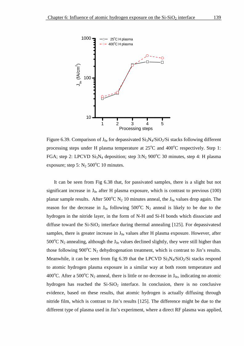
Chapter 6: Influence of atomic hydrogen exposure on the Si-SiO2 interface
139
1 2 3 4 510
100
1000
J 0e (
fA/c
m2 )
Processing steps
25oC H plasma 400oC H plasma
Figure 6.39. Comparison of J0e for depassivated Si3N4/SiO2/Si stacks following different
processing steps under H plasma temperature at 25oC and 400oC respectively. Step 1:
FGA; step 2: LPCVD Si3N4 deposition; step 3:N2 900oC 30 minutes, step 4: H plasma
exposure; step 5: N2 500oC 10 minutes.
It can be seen from Fig 6.38 that, for passivated samples, there is a slight but not
significant increase in J0e after H plasma exposure, which is contrast to previous (100)
planar sample results. After 500oC N2 10 minutes anneal, the J0e values drop again. The
reason for the decrease in J0e following 500oC N2 anneal is likely to be due to the
hydrogen in the nitride layer, in the form of N-H and Si-H bonds which dissociate and
diffuse toward the Si-SiO2 interface during thermal annealing [125]. For depassivatesd
samples, there is greater increase in J0e values after H plasma exposure. However, after
500oC N2 annealing, although the J0e values declined slightly, they were still higher than
those following 900oC N2 dehydrogenation treatment, which is contrast to Jin’s results.
Meanwhile, it can be seen from fig 6.39 that the LPCVD Si3N4/SiO2/Si stacks respond
to atomic hydrogen plasma exposure in a similar way at both room temperature and
400oC. After a 500oC N2 anneal, there is little or no decrease in J0e, indicating no atomic
hydrogen has reached the Si-SiO2 interface. In conclusion, there is no conclusive
evidence, based on these results, that atomic hydrogen is actually diffusing through
nitride film, which is contrast to Jin’s results [125]. The difference might be due to the
different type of plasma used in Jin’s experiment, where a direct RF plasma was applied,

Chapter 6: Influence of atomic hydrogen exposure on the Si-SiO2 interface
140
and it may be that H atoms had sufficient energy to be implanted deep in the nitride film.
Some of the SIMS results give some support for this [125].
6.8 Effect of low temperature thermal annealing on Si-
SiO2 stack following MW hydrogen plasma exposure
The work in this section is focused on investigating the thermal annealing behavior
of Si-SiO2 interface defects introduced by atomic hydrogen using carrier lifetime and
capacitance-voltage measurements. Because RTA cannot be used to give detailed
annealing characteristics; in an attempt to determine these characteristics, anneals will
be carried out at lower temperature and lifetime/J0e measurements carried out
periodically during the anneal. Previous work [125-127] has shown that the defects are
thermally unstable, however detailed properties of the defects have not been
investigated.
Samples following H plasma exposure were put into the TIDLS chamber in air or
N2 atmosphere. The wafer can reach the target temperature within about 120 seconds.
Lifetime measurements were carried out automatically at regular time intervals during
the anneal process. The time interval between measurements can be varied according to
requirements and 2 measurements were taken for each time interval to obtain an average.
Figure 6.40 shows the J0e dependence on annealing time and temperature for H
plasma exposed samples. Five initially oxidised and passivated samples were used.
After plasma exposure, a thermal anneal was carried out at temperatures in the range of
120-240oC for up to 20 hours in air to remove plasma-induced defects. H plasma
conditions are standard with MW power 300W. The starting points at zero were just
after H plasma exposure and the first annealing points were measured after 3 minutes
stabilization at set temperature in TIDLS chamber. Fig 6.40 was arrived at as follows:
Firstly, the J0e values measured at elevated temperatures were converted to room
temperature J0e values, using the pair of J0e values (one at elevated and one at room
temperature) for each sample at the end of the anneal process. After that, the initial J0e
(measured prior to atomic H exposure) was subtracted, since this represents the
contribution to J0e from thermally stable, unpassivated defects which will not be
significantly affected by the atomic H exposure. Finally, J0e for each curve was
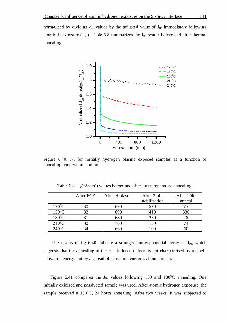
Chapter 6: Influence of atomic hydrogen exposure on the Si-SiO2 interface
141
0 400 800 12000.0
0.2
0.4
0.6
0.8
1.0
Nor
mal
ized
J0e
den
sity
(J0e
/J0e
i)
Anneal time (min)
120oC 150oC 180oC 210oC 240oC
normalised by dividing all values by the adjusted value of J0e immediately following
atomic H exposure (J0ei). Table 6.8 summarizes the J0e results before and after thermal
annealing.
Figure 6.40. J0e for initially hydrogen plasma exposed samples as a function of annealing temperature and time. Table 6.8. J0e(fA/cm2) values before and after low temperature annealing.
The results of fig 6.40 indicate a strongly non-exponential decay of J0e, which
suggests that the annealing of the H – induced defects is not characterised by a single
activation energy but by a spread of activation energies about a mean.
Figure 6.41 compares the J0e values following 150 and 180oC annealing. One
initially oxidised and passivated sample was used. After atomic hydrogen exposure, the
sample received a 150oC, 24 hours annealing. After two weeks, it was subjected to
After FGA After H plasma After 3min stabilization
After 20hr anneal
120oC 30 690 570 510 150oC 32 690 410 330 180oC 31 680 250 130 210oC 30 700 150 74 240oC 34 660 100 60

Chapter 6: Influence of atomic hydrogen exposure on the Si-SiO2 interface
142
0 1000 2000 3000 4000
200
400
600
800
1000
J 0e (
fA/c
m2 )
Annealing time (min)
150oC 24hrs after 2 weeks 150oC anneal 24hrs followed by 180oC anneal 22hrs
another 150oC, 24 hours annealing and a subsequent 180oC, 22 hours annealing were
carried out successively.
Fig. 6.41. Comparison J0e values for a H plasma exposed sample followed by successive
150oC (x2) and 180oC anneals. H plasma conditions are standard with MW 300W.
The discontinuity in the J0e values (in fig 6.41) between the first and second 150oC
anneals is most likely the result of some degradation of the oxide in this period of time.
However, the rate of decrease of J0e at the beginning of the second 150oC anneal is
approximately the same as at the end of the first 150oC anneal, as would be expected.
When the anneal temperature is increased to 180oC, there is a sudden and large decrease
in J0e, suggesting the removal (annealing) of some defects which were only removed
very slowly at 150oC. This provides further evidence for a spread in activation energies
for the removal of the thermally unstable defects.
Figure 6.42 compares the J0e values between measuring values (fig 6.40) and
calculated values from equation 6.2. More sophisticated models, which assume various
distributions of activation energies, can be applied in attempt to fit the experimental data.
One possibility is a Gaussian distribution of activation energies about a mean value, see
equation (6.2) [23].
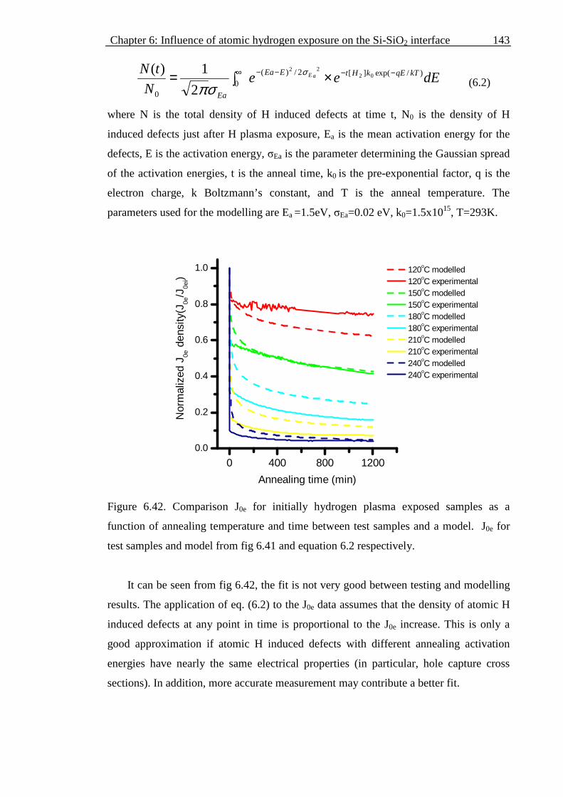
Chapter 6: Influence of atomic hydrogen exposure on the Si-SiO2 interface
143
0 400 800 12000.0
0.2
0.4
0.6
0.8
1.0
Nor
mal
ized
J0e
den
sity
(J0e
/J0e
i)
Annealing time (min)
120oC modelled 120oC experimental 150oC modelled 150oC experimental 180oC modelled 180oC experimental 210oC modelled 210oC experimental 240oC modelled 240oC experimental
dEeeN
tN kTqEkHtEEa
Ea
aE )/exp(][2/)(0
0
0222
2
1)( −−−−∞ ×∫= σ
σπ (6.2)
where N is the total density of H induced defects at time t, N0 is the density of H
induced defects just after H plasma exposure, Ea is the mean activation energy for the
defects, E is the activation energy, σEa is the parameter determining the Gaussian spread
of the activation energies, t is the anneal time, k0 is the pre-exponential factor, q is the
electron charge, k Boltzmann’s constant, and T is the anneal temperature. The
parameters used for the modelling are Ea =1.5eV, σEa=0.02 eV, k0=1.5x10¹⁵, T=293K.
Figure 6.42. Comparison J0e for initially hydrogen plasma exposed samples as a
function of annealing temperature and time between test samples and a model. J0e for
test samples and model from fig 6.41 and equation 6.2 respectively.
It can be seen from fig 6.42, the fit is not very good between testing and modelling
results. The application of eq. (6.2) to the J0e data assumes that the density of atomic H
induced defects at any point in time is proportional to the J0e increase. This is only a
good approximation if atomic H induced defects with different annealing activation
energies have nearly the same electrical properties (in particular, hole capture cross
sections). In addition, more accurate measurement may contribute a better fit.

Chapter 6: Influence of atomic hydrogen exposure on the Si-SiO2 interface
144
-12 -10 -8 -6 -4 -2 0 2 40.0
0.2
0.4
0.6
0.8
1.0
C/C
i
Applied voltage (V)
control without H plasma after H plasma
after 180oC 3 min
after 180oC 10 min
after 180oC 25 min
after 180oC 60 min
after 180oC 150 min
after 180oC 150 min and 240oC 24 hr
passivated sample HFCV
To complement the lifetime results, C-V measurements were carried out. CV
samples received identical H plasma exposure processing as those lifetime samples in
fig 6.40. After H plasma exposure, samples were annealed in the TIDLS chamber under
a N2 atmosphere in an analogous fashion to the lifetime samples. Samples were initially
heated to 180oC for different times. This was followed by a 240oC 24 hour anneal.
Figure 6.43 shows the high-frequency curve and figure 6.44 shows the corresponding
Dit distribution of an initially passivated sample. C-V measurements were carried out
after the sample had cooled down to room temperature. The same metal dot was
measured every time. Figures 6.45 and 6.46 show the corresponding results for an
initially depassivated sample that received otherwise identical treatment. For
comparison, two as oxidized and hydrogenated (after stand FGA) or dehydrogenated
(after an RTA 700oC in N2) MOS stacks are also shown in fig 6.43 and 6.45
respectively. Figure 6.47 shows the dependence of (a) the midgap Dit and (b) interface
charge density on the annealing time at 180oC for passivated and depassivated H plasma
exposed samples. Table 6.9 summarizes the influence of annealing time and
temperature on p-type Si-SiO2 interface properties.
Fig 6.43. HFCV curves for hydrogen plasma exposed passivated sample following
annealing at 180oC for different times and a successive 240oC 24 hours in N2.

Chapter 6: Influence of atomic hydrogen exposure on the Si-SiO2 interface
145
0.2 0.4 0.6 0.8
1E8
1E9
1E10
1E11
1E12
1E13
1E14
Dit (
eV-1cm
-2)
Bandgap energy (eV)
control without H plasma after H plasma
after 180oC 3 min after 180oC 10 min
after 180oC 25 min
after 180oC 60 min
after 180oC 150 min after 180oC 150 min and 240oC 24hr
passivated sample
-12 -8 -4 0 40.0
0.2
0.4
0.6
0.8
1.0
C/C
i
Applied voltage (V)
control without H plasma after H plasma
after 180oC 3 min
after 180oC 10 min
after 180oC 25 min
after 180oC 60 min
after 180oC 150 min
after 180oC 150 min and 240oC 24hr
depassivated sample HFCV
\
Figure 6.44. Dit distribution for hydrogen plasma exposed passivated sample subject to
identical processing in fig 6.43.
Fig 6.45. HFCV curves for hydrogen plasma exposed depassivated sample following
annealing at 180oC for different times and a successive 240oC 24 hours in N2.
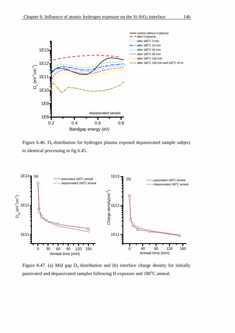
Chapter 6: Influence of atomic hydrogen exposure on the Si-SiO2 interface
146
0 40 80 120 160
1E11
1E12
1E13
Cha
rge
dens
ity(c
m-2)
Anneal time (min)
passivated 180oC anneal depassivated 180oC anneal
(b)
0.2 0.4 0.6 0.81E8
1E9
1E10
1E11
1E12
1E13
Dit (
eV-1cm
-2)
Bandgap energy (eV)
control without H plasma after H plasma
after 180oC 3 min
after 180oC 10 min
after 180oC 25 min
after 180oC 60 min
after 180oC 150 min
after 180oC 150 min and 240oC 24 hr
depassivated sample
0 30 60 90 120 150
1E11
1E12
1E13
Ditm
(eV
-1cm
-2)
Anneal time (min)
passivated 180oC anneal depassivated 180oC anneal
(a)
Figure 6.46. Dit distribution for hydrogen plasma exposed depassivated sample subject
to identical processing in fig 6.45.
Figure 6.47. (a) Mid gap Dit distribution and (b) interface charge density for initially
passivated and depassivated samples following H exposure and 180oC anneal.

Chapter 6: Influence of atomic hydrogen exposure on the Si-SiO2 interface
147
Table 6.9. The interface charge density Q(×1011cm-2) and Midgap interface defect density
Ditm(×1011eV-1cm-2) before and after H plasma and following annealing at 180oC and
240oC in a succession.
Several conclusions can be drawn from above results. Firstly, both initially
passivated and depassivated samples show a rapid decrease in charge density following
short anneals at 180oC. The decay of the charge follows a similar curve to the decrease
of midgap Dit, suggesting that the same kind of defect is responsible for both. It is worth
to note that there is a significant increase in interface charge after hydrogen plasma
exposure compared to previous results. This may be due to experimental error as before
-slightly different exposure conditions every time resulting in different H plasma
density and uniformity. Secondly, the distribution of Dit is relatively uniform over the
entire band-gap energy range; defects closer to the valence band edge appear to be
removed slightly faster than others. Thirdly, the annealing behaviour of initially
passivated and depassivated samples is very similar. Finally, the decay of Dit and Q
shows the same general behaviour as the decrease in J0e following annealing, exhibiting
strongly non-exponential behaviour which implies a spread of activation energies.
6.9 Summary
The results show that, consistent with earlier observations, atomic H exposure
results in the generation of additional defects at the Si-SiO2 interface. These defects are
efficient carrier recombination centres, are thermally unstable and can be effectively
passivated After
FGA
400oC
After
plasma
After
180oC
3mins
After
180oC
10mins
After
180oC
25mins
After
180oC
60mins
After
180oC
150mins
After
240oC
24hr
Ditm 0.02 58 7.7 4.4 3.0 2.3 1.6 0.055
Q 0.75 22 3.4 2.1 1.5 1.3 0.94 0.045
depassivated After
RTA
700oC
After
plasma
After
180oC
3mins
After
180oC
10mins
After
180oC
25mins
After
180oC
60mins
After
180oC
150mins
After
240oC
24hr
Ditm 3.2 43 6.1 3.9 2.9 2.0 1.3 0.088
Q 1.5 19 3.2 2.3 1.8 1.4 1.0 0.15

Chapter 6: Influence of atomic hydrogen exposure on the Si-SiO2 interface
148
removed by a short RTA anneal at 300oC or above. Furthermore, TIDLS anneal results
show that even at lower temperature (240oC) in air or N2, most thermally unstable
defects can also be removed by longer annealing time. The annealing of this thermally
unstable defect is not characterized by a single activation energy but rather by a spread
of activations energies. In addition, it looks like higher plasma exposure pressure
accelerates the reaction but higher exposure power (above 400W) will introduce some
permanent damage which can not be removed completely by subsequent thermal
treatments.
Atomic H exposure does not appear to have a significant effect on the density of
thermally stable Pbx centres. Following sufficiently long atomic H exposure times, the
fraction of unpassivated Pbx centres reaches a steady-state value which is independent of
the initial passivation state of the interface. The degree of steady-state passivation
shows no discernible dependence on temperature in the range 25-600oC during atomic
H plasma exposure, in agreement with previous predictions [40]. In particular, at all
sample temperatures in the range 25-600oC, the efficiency of defect passivation by H is
lower than that afforded by H2. The similar behaviour is observed between phosphorous
diffused and undiffused samples and also between (100) planar samples and (111)
planar and (100) textured samples, indicating that the presence of a phosphorous
diffusion layer does not fundamentally alter the physics of interface passivation and the
response to atomic hydrogen is insensitive to crystal orientation.
This result has significant implications for silicon solar cells. The front surfaces of
most crystalline silicon solar cells feature a layer of silicon nitride (SiNx) deposited by
plasma-enhanced chemical vapour deposition, which acts as an antireflection coating, a
surface passivation layer and a source of hydrogen for bulk passivation. At elevated
temperatures, atomic hydrogen is released from the nitride film and driven into the bulk,
where it passivates defects. The interface region of such cells consists of an oxynitride
layer. In addition, stacks consisting of a thin layer of SiO2 and a thicker film of SiNx are
also under active consideration since such stacks can, in principle, combine the
advantages of the Si-SiO2 interface (low Dit) with the benefits of SiNx. Recently,
excellent surface passivation has also been demonstrated by thin Al2O3 films prepared
by atomic layer deposition and it was verified that an interfacial oxide layer of about
1.5nm is present between the silicon and Al2O3 as a result of the deposition process
[128]. It is noted that, while it is difficult to compare the total hydrogen flux released
during silicon nitride layer deposition and subsequent thermal treatments, and the
hydrogen flux during the experiments described here, possible differences in the total

Chapter 6: Influence of atomic hydrogen exposure on the Si-SiO2 interface
149
flux are unlikely to have a significant impact on the results because the fraction of
passivated interface defects reaches a steady state value.
The results suggest that, for oxide/nitride stacks in particular, there is no conclusive
evidence that atomic hydrogen is actually diffusing through nitride film, which is
contrast to previous results.

Chapter 6: Influence of atomic hydrogen exposure on the Si-SiO2 interface
150
Chapter 7: Effect of corona charging, humidity, UV exposure and mineral acid on the Si-SiO2 interface
151
CHAPTER 7
Effect of corona charging, humidity, UV
exposure and mineral acid on the Si-SiO2
interface
In this chapter, the effect of corona charging, humidity, UV exposure and mineral
acid on the Si-SiO2 has been investigated. Especially, the purpose of the work in this
chapter is to see to what extent of the annealing behaviour of the resulting defects (as
measured by J0e and Dit) is similar to that of the defects introduced by atomic hydrogen
from a plasma, as was done in the previous chapter.

Chapter 7: Effect of corona charging, humidity, UV exposure and mineral acid on the Si-SiO2 interface
152
7.1 Effect of corona charging and following thermal
anneal on Si-SiO2 stacks
Corona charging, as an effective means of introducing external charges to the
surface region, has been widely used for research purposes in photovoltaics due to the
field-effect passivation it provides. It has been shown in the literature that corona
charging can affect the Si band bending and surface recombination velocity of the Si-
SiO2 structure dramatically [129]. Surface recombination velocities lower than 1cm/s
can be achieved with corona charging [130]. However, degradation can occur when the
electric field is high (typically ~6MV/cm, i.e. sufficiently large to result in an
appreciable tunnelling current). The damage resulting from corona charging with high
electric fields is often attributed to hot electrons leading to H liberation, either in the
oxide or at the oxide surface. The atomic hydrogen is then believed to diffuse to the Si-
SiO2 interface where it creates interface defects [46].
In this section, we experimentally investigate the influence of corona charging and
subsequent thermal anneals on the surface passivation of the Si-SiO2 interface in more
detail. The corona charges were generated by applying a voltage of 10kV to a steel
needle about 5cm above the samples. On samples for lifetime measurements, corona
charging was carried out on both sides, sequentially, for equal amounts of time. On
samples for C-V measurements, corona charging was carried out only on the oxidized
surface on which the measurement was performed.
Samples used for lifetime measurements were p-type, 100Ω.cm, (100), FZ wafers.
After standard processing, samples received corona charging and IPA rinse. CZ, p-type,
(100), 8-12Ω.cm samples were used for C-V measurements. C-V samples were
processed together with the lifetime samples except for the phosphorous treatment.
7.1.1 Effect of corona charging and post corona RTA on the
Si-SiO2 surface passivation
Table 7.1 shows the variation of the effective lifetime and J0e with processing steps
for negative corona charged Si-SiO2 stacks. A negative 10kV voltage was applied
without grid between sample and needle. Five oxidised and corona charged samples
were used and average values are shown. Figure 7.1 shows the variation of (a) the
effective lifetime and (b) J0e with RTA time and temperatures for negative corona

Chapter 7: Effect of corona charging, humidity, UV exposure and mineral acid on the Si-SiO2 interface
153
0 50 100 150 200 250 300
100
1000
10000
Effe
ctiv
e li
fetim
e (µ
s)
Annealing time (s)
200oC 300oC 400oC 450oC 500oC
(a)
charged samples. Prior to RTA treatments, the samples had received the treatments
detailed in table 7.1. Five oxidised and corona charged samples were used - one for each
corresponding RTA annealing temperature. Figure 7.2 shows the dependence of midgap
Dit on RTA temperature for a sample that received 5 minutes positive corona charging
and a control sample (no corona charging). The samples had initially been de-
hydrogenated with a 700oC RTA for 3 minutes.
Table 7.1. Processing steps and corresponding effective lifetime(µs) and Emitter
saturation current density J0e (fA/cm2)
Processing steps
Description Average effective lifetime
Emitter saturation current density J0e
Step1 Standard processing 5500 17 Step2 RTA
700oC, 3minutes 430
380
Step3 negative corona charging 5 minutes/side
850
160
Step4 Removing charges by IPA and RCA
160 440

Chapter 7: Effect of corona charging, humidity, UV exposure and mineral acid on the Si-SiO2 interface
154
0 100 200 300
100
1000J 0e
(fA
/cm
2 )
Annealing time (s)
200oC 300oC 400oC 450oC 500oC
(b)
200 250 300 350 400 450 5001E10
1E11
1E12
Ditm
(eV
-1cm
-2)
Annealing temperature (oC)
positive corona charging control without corona charging
Figure 7.1. (a) Effective lifetime of samples following processing steps in table 7.1 and
subsequent RTA in N2 for 30 to 300 seconds at temperatures ranging from 200oC to
500oC. Starting points corresponding to those of step 4 in table 7.1, (b) corresponding
J0e.
Figure 7.2. Midgap Dit vs RTA temperatures for positive corona charged and no corona
charged control samples.
Chapter 7: Effect of corona charging, humidity, UV exposure and mineral acid on the Si-SiO2 interface
155
It can be seen from table 7.1 that, after an RTA at 700oC, the lifetime decreases and
J0e increases dramatically due to the loss of hydrogen from the Si-SiO2 interface. Corona
charging then causes an increase of the effective lifetime and decrease of J0e, which is
attributed to the field passivation effect resulting from the high density of negative
charge resulting from corona charging: the deposited corona charges create an electric
field across Si-SiO2 interface, which reduces the surface concentration of minority
carriers so that the surface recombination velocity decreased and effective lifetime is
increased [129, 130]. After removing the charges by IPA and an RCA clean, the
lifetime declines and J0e rises again (step 4). After step 4, the lifetime is lower and J0e is
higher than those after step 2. It is therefore clear that the corona charging process has
resulted in damage to the Si-SiO2 interface.
It is clear from fig 7.1 that the passivation quality improves with increasing RTA
temperature up to 400oC. This indicates a removal of the unstable interface defects
introduced by the corona charging process, consistent with that observed for atomic
hydrogen [26]. Above 400oC, the lifetime decreases and the values of J0e increase
because anneals above 400oC can result in the loss of hydrogen from the Si-SiO2
interface, but do not modify the interface in other ways. The results strongly suggest
that the corona charging introduced additional hydrogen to passivate a fraction of the
(stable) interface defects, because the effective lifetime is higher, and J0e is lower,
following a suitable RTA treatment after corona charging, than for the sample in the de-
hydrogenated state (step 2 in table 7.1).
It can be seen from fig 7.2 that, compared with the control sample, a substantial
decrease in midgap Dit is observed for the corona charged sample between RTA
annealing temperatures 200oC and 450oC for 3 minutes, and an increase at 500oC can
also be observed. The C-V results from positive corona charging are consistent with the
lifetime results from negative charging. The very high Dit values measured after positive
corona charging are chiefly the result of non-paramagnetic defects, since the majority of
the defects are removed by a short RTA treatment. The results therefore support the
conclusion that the corona damage is mainly due to atomic hydrogen.
The results confirm that corona charging results in the introduction of additional
defects to the Si-SiO2 interface, and show that these defects can be subsequently
removed by an RTA treatment, which are consistent with previous results [26]. Further,
both lifetime and C-V measurements strongly suggest that hydrogen has been
introduced to the interface [131]. The damage observed following corona charging and

Chapter 7: Effect of corona charging, humidity, UV exposure and mineral acid on the Si-SiO2 interface
156
0 400 800 1200
0.1
1
Nor
mal
ized
J0e
den
sity
(J0e
/J0e
i)
Annealing time (min)
120oC
150oC
180oC
210oC
the removal of this damage following subsequent RTA treatments, are all consistent
with the effects of hydrogen on the Si-SiO2 interface [40]. The application of a large
electric field - as was created here - leads to tunnelling of carriers across the oxide. In
the case of negative corona charging, the likely mechanism is the tunnelling of electrons
from the SiO2 to the Si; in the case of positive corona charging electrons tunnel from the
Si to the SiO2. In either case, it appears that the energetic electrons liberate atomic
hydrogen in the SiO2, which causes the observed changes in Dit and surface passivation.
7.1.2 Detailed investigation of annealing behaviour of defects
introduced by corona charging
In this section, the thermal stability of Si-SiO2 interface defects by corona charging
is investigated in more detail. Figure 7.3 shows the dependence of J0e on annealing time
and temperature for samples following corona charging. Four initially oxidised
passivated samples are used. Corona charging was used to create a very high electric
field across the oxide (>6MV/cm) to cause tunnelling of electrons from the silicon
substrate across the oxide. The starting points at time zero in fig 7.3 are just after corona
charging and before thermal annealing. The J0e values were normalized using the
procedure employed for the results in fig 6.41. J0ei is the adjusted value of J0e
immediately following corona charging. Table 7.2 summarizes the J0e results before and
after thermal annealing.
Figure 7.3. J0e dependence of annealing time and temperature after Corona charging.

Chapter 7: Effect of corona charging, humidity, UV exposure and mineral acid on the Si-SiO2 interface
157
Table 7.2. J0e (fA/cm2) values before and after corona charging and annealing.
It can be seen from fig 7.3 that the J0e values of corona charged samples reduce
quickly during the first a few minutes of annealing and then enter a regime where it is
only weakly affected by the longer annealing time. This result is in agreement with
those in fig 6.41 in which it has been shown that H plasma exposure caused thermally
unstable defects on Si-SiO2 stack can be effectively removed by low temperature
annealing. Similarly, with increasing annealing temperatures, the J0e values can recover
to a level that is closer to the initial value (prior to charging). For a specific annealing
temperature, annealing times longer than ~200-400 minutes do not result in a significant
further decrease of J0e. In general, the annealing behaviour of the samples following
corona charging is qualitatively similar to that of samples exposed to atomic H (fig
6.41). However, there are significant differences in the shapes of the decay curves.
To illustrate this, figure 7.4 compares the J0e dependence on annealing time for
corona charged and PECVD hydrogen plasma exposed samples after annealing at 180
and 210oC respectively, using the data from figs 6.41 and fig 7.3.
Annealing temperature
After FGA After corona and IPA
After anneal
120oC 30 200 86 150oC 32 220 61 180oC 31 250 49 210oC 30 170 37
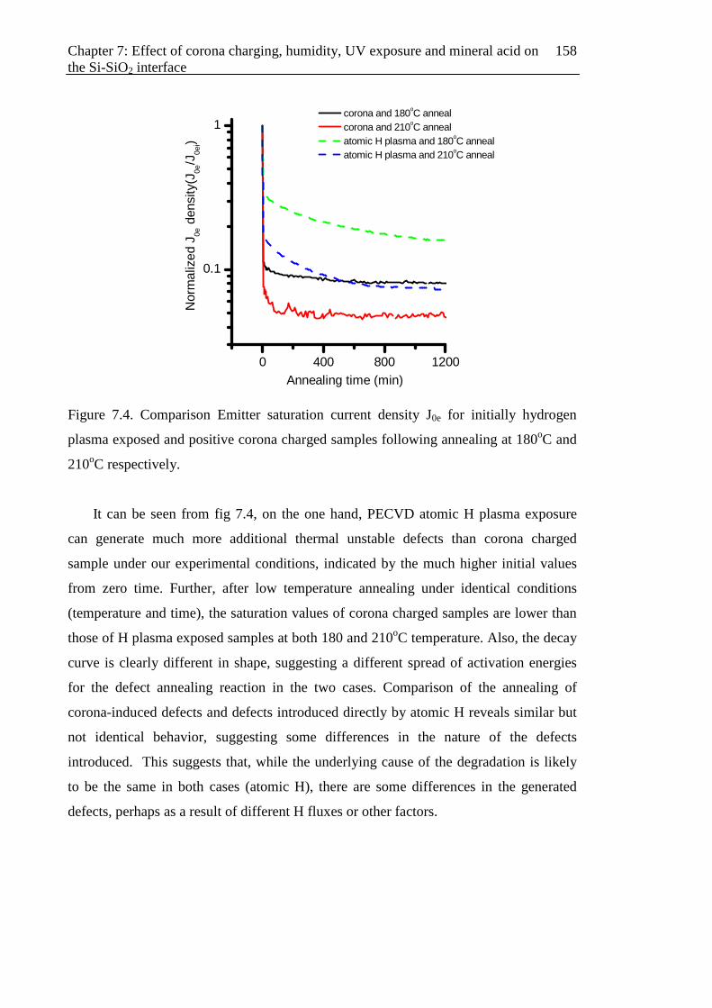
Chapter 7: Effect of corona charging, humidity, UV exposure and mineral acid on the Si-SiO2 interface
158
0 400 800 1200
0.1
1
Nor
mal
ized
J0e
den
sity
(J0e
/J0e
i)
Annealing time (min)
corona and 180oC anneal corona and 210oC anneal atomic H plasma and 180oC anneal atomic H plasma and 210oC anneal
Figure 7.4. Comparison Emitter saturation current density J0e for initially hydrogen
plasma exposed and positive corona charged samples following annealing at 180oC and
210oC respectively.
It can be seen from fig 7.4, on the one hand, PECVD atomic H plasma exposure
can generate much more additional thermal unstable defects than corona charged
sample under our experimental conditions, indicated by the much higher initial values
from zero time. Further, after low temperature annealing under identical conditions
(temperature and time), the saturation values of corona charged samples are lower than
those of H plasma exposed samples at both 180 and 210oC temperature. Also, the decay
curve is clearly different in shape, suggesting a different spread of activation energies
for the defect annealing reaction in the two cases. Comparison of the annealing of
corona-induced defects and defects introduced directly by atomic H reveals similar but
not identical behavior, suggesting some differences in the nature of the defects
introduced. This suggests that, while the underlying cause of the degradation is likely
to be the same in both cases (atomic H), there are some differences in the generated
defects, perhaps as a result of different H fluxes or other factors.

Chapter 7: Effect of corona charging, humidity, UV exposure and mineral acid on the Si-SiO2 interface
159
7.2 Effect of humidity on the properties of the Si-SiO2
interface
Ensuring long term solar cell reliability to environmental exposure is a critical
factor for photovoltaic applications. It is well known that moisture can reduce solar cell
module reliability in a number of ways [132]. Lancellotti et al. [133] studied the effect
of humidity on Si solar cells. In their experiments, FZ, p-type, (100), 0.3Ω.cm samples
were used to fabricate the solar cell devices, which were exposed to an oven at 95oC
with 100% humidity. The results show that following 60 hours exposure, the short
circuit current decreased about 2%, and the integrated External Quantum Efficiency
decreased 1% after 15 hours and a further 1% after 59 hours. In this section, some
experiments were carried out to examine the effect of moisture on the Si-SiO2 interface
and the following thermal anneal results were compared to those of atomic hydrogen
exposure and corona charging.
The Samples used for lifetime are FZ, p-type, (100), 100-1000Ω.cm, passivated,
and FZ, n-type, (111), 91-109Ω.cm, depassivated. After standard phosphorous diffusion
processing, samples received an oxidation at 1000oC for 1 hour or 30 minutes for (100)
and (111) samples respectively followed by 30 minutes in situ N2 anneal.
Hydrogenation was realized by FGA 400oC 30 minutes and de-hydrogenation was
realized by RTA 700oC 3 minutes in N2. Both passivated and depassivated samples
were put in a saturated humidity cabinet. Humidity conditions were: temperature 80oC,
humidity concentration 100 per cent, time a week. After humidity exposure, passivated
sample received an annealing at 180oC for 24 hours and followed by a 240oC for 5
hours, while depassivated samples received a RTA annealing at 300oC in N2 for 1
minute.
Table 7.3 summarizes the J0e values of passivated and depassivated samples before
and after humidity exposure and annealing. Figure 7.5 shows the J0e dependence on
annealing time and temperature for passivated samples after humidity exposure, and
figure 7.6 compares the J0e dependence of annealing time at 180oC for passivated
samples after humidity exposure, corona charging and atomic hydrogen exposure
respectively.
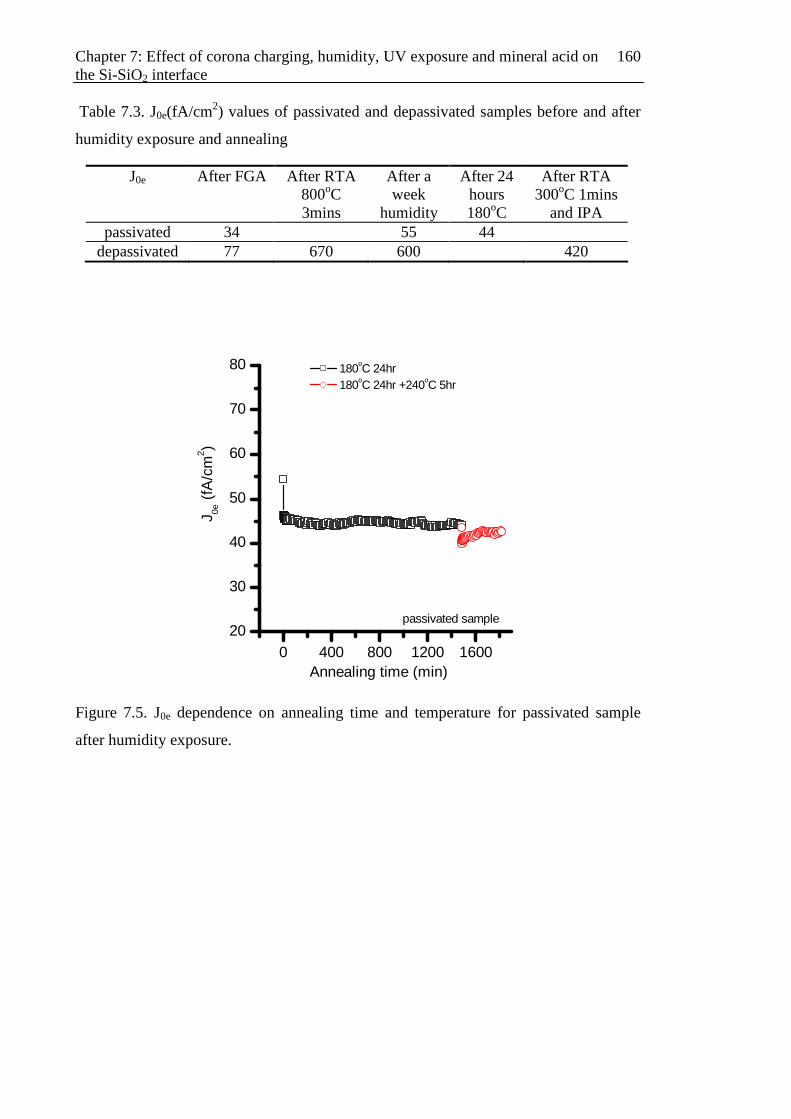
Chapter 7: Effect of corona charging, humidity, UV exposure and mineral acid on the Si-SiO2 interface
160
0 400 800 1200 160020
30
40
50
60
70
80
J 0e (
fA/c
m2 )
Annealing time (min)
180oC 24hr 180oC 24hr +240oC 5hr
passivated sample
Table 7.3. J0e(fA/cm2) values of passivated and depassivated samples before and after
humidity exposure and annealing
Figure 7.5. J0e dependence on annealing time and temperature for passivated sample
after humidity exposure.
J0e After FGA After RTA 800oC 3mins
After a week
humidity
After 24 hours 180oC
After RTA 300oC 1mins
and IPA passivated 34 55 44
depassivated 77 670 600 420

Chapter 7: Effect of corona charging, humidity, UV exposure and mineral acid on the Si-SiO2 interface
161
0 400 800 1200 16000
200
400
600
800
J 0e (
fA/c
m2 )
Annealing time (min)
80oC humidity a week and 180oC 24hr positive 10kV 2hr/side corona and 180oC 24hr RT atomic H plasma and 180oC 24hr
Figure 7.6. Comparison the J0e dependence of annealing time for passivated samples
after humidity exposure, corona charging and atomic hydrogen plasma exposure
respectively and following 180oC annealing.
It can be seen from table 7.3, after the humidity exposure under our experimental
conditions, the general trend of the interface modification – for passivated samples,
there is degradation and for depassivated sample, there is an improvement after
exposure and thermal treatments, is largely consistent with the effect of atomic
hydrogen on the Si-SiO2 interface. Meanwhile, it can be seen in fig 7.5 that the J0e
values do not decline further following higher annealing temperature and the J0e values
remain at almost the same level at 180 and 240oC, which is inconsistent to atomic H
exposed and corona charged samples. Finally, it is clear from fig 7.6 that, by comparing
humidity exposure, corona charging and atomic H plasma exposed samples after 180oC
annealing, there is a clear difference in the J0e dependence of annealing time between
hydrogen plasma exposure and corona charging and humidity exposure. Although the
reasons for this difference are not clearly understood at present, several plausible factors
are responsible for this difference such as the dose of atomic hydrogen, the stress
applied on the Si-SiO2 interface and some other H related species introduced into the Si-
SiO2 stack.

Chapter 7: Effect of corona charging, humidity, UV exposure and mineral acid on the Si-SiO2 interface
162
7.3 Effect of UV illumination on the Si-SiO2 surface
passivation
Many works have discussed how ultraviolet light can excite electrons from silicon
into silicon dioxide, and how this can lead to the creation of interface states. Most of
these experiments have been done on MOS capacitors in which a field drives the
electrons into the oxide during UV exposure and a current through the oxide is
measured.
In addition to experiments involving MOS capacitors, much of the work in this
section uses diffused, oxidised wafers with voltage applied by corona charging across
the oxide during UV exposure. Evidence that damage is caused by UV illumination is
presented and the effects of oxidation variables on the stability of the Si-SiO2 interface
were examined. UV exposures were done with either sunlight or a Halogen lamp.
Figure 7.7 shows the variation of the effective lifetime and J0e with sunshine
illumination time for positive corona charged Si-SiO2 samples. Lifetime samples
received standard phosphorous diffusion and followed by two different oxidations (dry
oxidation and TCA oxidation) to get nearly identical oxide thickness (about 50 nm).
After that, two samples-one dry oxidised and one TCA oxidised, received FGA
treatment. Finally, all samples received positive corona charging and followed by sun
shine exposure on both sides for identical time. Corona charge conditions are positive
8kV, 5 minutes, a steel grid was put between needle and sample to prevent charging
damage and make uniform charge distribution. Starting points are from those following
corona charging. Four oxidised and corona charged samples are used.

Chapter 7: Effect of corona charging, humidity, UV exposure and mineral acid on the Si-SiO2 interface
163
0 2 4 6 8 102000
3000
4000
5000
6000
7000
8000
9000
Effe
ctiv
e lif
etim
e (µ
s)
Sunshine illumination time (hr)
TCA oxidation Dry oxidation TCA oxidation and FGA Dry oxidation and FGA
(a)
0 2 4 6 8 10
25
30
35
40
45
50
55
60
65
J 0e (
fA/c
m2 )
Sunshine illumination time (hr)
TCA oxidation Dry oxidation TCA oxidation and FGA Dry oxidation and FGA
(b)
Figure 7.7. (a) Effective lifetime and (b) J0e for initially corona charged samples as a
function of sunshine illumination time.
It can be seen from fig 7.7 that, on the one hand, the degree of degradation during
UV exposure is much higher for TCA oxidised samples than those dry oxidised samples.
On the other hand, for TCA oxidised samples, the FGA treatment can further result in
degradation. The results indicate that hydrogen content in SiO2 film plays a crucial role
in the degradation of Si-SiO2 stack during UV exposure. One reasonable mechanism
behind this phenomenon is that energetic electrons are injected from Si substrate into

Chapter 7: Effect of corona charging, humidity, UV exposure and mineral acid on the Si-SiO2 interface
164
0 1 2 3 4 5 6 7 830
35
40
45
50
55
60
65
J 0e (
fA/c
m2 )
Halogen lamp illumination time (hr)
TCA oxidation and FGA
the oxide and release the atomic hydrogen in it, which subsequently diffuse to the Si-
SiO2 interface and generate defects.
Figure 7.8 shows the variation of J0e with halogen lamp illumination time for
positive corona charged Si-SiO2 samples. Lifetime samples received standard
phosphorous diffusion and followed by 1000oC TCA oxidation 34 minutes, N2 in situ
30 minutes and FGA successively. Two 300W halogen lamps used as UV sources are
set on the top of samples and distance between sample and lamp is about 20cm. Starting
points are following immediately corona charging. The straight dashed line in fig 7.8
represents the initial value before corona charging.
Figure 7.8. Emitter saturation current density J0e for initially corona charged samples as
a function of halogen lamp illumination time.
Compared with the line of TCA oxidation and FGA in fig 7.7, the increment of J0e
is similar, which suggests that the damage caused by sunlight is similar to that caused
by UV light in halogen lamp.
An interesting question is whether the hydrogen source is from the dielectric film or
from the interface of dielectric and air. To further elucidate this, a SiN-SiO2-Si stack
was designed to research the hydrogen source. Figure 7.9 shows the variation of the
effective lifetime and J0e with sunshine illumination time for positive corona charged Si-

Chapter 7: Effect of corona charging, humidity, UV exposure and mineral acid on the Si-SiO2 interface
165
0 2 4 6 8 10
3000
3500
4000
4500
5000
5500
6000
Eff
ectiv
e lif
etim
e(µs
)
Sunshine illumination time (hr)
50 nm SiO2/50 nm LPCVD Si
3N
4(a)
0 2 4 6 8 10
40
45
50
55
60
65
70
75
80
85
J 0e(f
A/c
m2 )
Sunshine illumination time (hr)
50 nm SiO2/50 nm LPCVD Si
3N
4(b)
SiO2-LPCVD Si3N4 samples. Lifetime samples received standard phosphorous diffusion
and followed by 1000oC TCA oxidation 34 minutes, N2 in situ 30 minutes and FGA
successively. Finally, 50nm LPCVD Si3N4 was deposited on the top of SiO2, the
LPCVD Si3N4 can impede the hydrogen in atmospheric moisture from diffusing into
SiO2 film. Starting points are from those following corona charging. The straight dashed
line in fig 7.9 represents the initial value before corona charging.
Figure 7.9. (a) Effective lifetime and (b) Emitter saturation current density J0e for
initially corona charged samples as a function of sunshine illumination time.

Chapter 7: Effect of corona charging, humidity, UV exposure and mineral acid on the Si-SiO2 interface
166
0 2 4 6 835
40
45
50
55
60
65
70
75
80
J 0e (
fA/c
m2 )
Halogen lamp illumination time (hr)
dry oxide + PECVD SiN TCA oxide + PECVD SiN
It can be seen results from the figure 7.9 that, even with the LPCVD Si3N4 film
impeding the invasion of moisture in the air into the SiO2 film, degradation is still
occurring in the Si-SiO2 interface. And this degradation is believed mainly due to the
hydrogen species existing in the TCA oxidised SiO2 film.
Figure 7.10 shows the variation of J0e with halogen lamp illumination time for
positive corona charged Si-SiO2-PECVD SiN samples. Before corona charging, lifetime
samples received standard phosphorous diffusion and followed by 1000oC TCA
oxidation 34 minutes and dry oxidation 60 minutes respectively to get nearly identical
oxide thickness. After that, samples received N2 in situ 30 minutes and FGA
successively. Finally, 30nm PECVD SiN was deposited on the top of SiO2 and followed
by 400oC N2 30 minutes anneal. Starting points are from those following corona
charging.
Figure 7.10. Emitter saturation current density J0e for initially corona charged samples
as a function of halogen lamp illumination time, comparing dry oxide and PECVD SiN
stacks to TCA oxide and PECVD SiN stacks.
By comparing with two different stacks, although the starting points are different,
there is a bigger increment for the TCA oxide stack. After halogen lamp illumination,
the increment is 23fA/cm2 and 8fA/cm2 for TCA oxide stack and dry oxide stack

Chapter 7: Effect of corona charging, humidity, UV exposure and mineral acid on the Si-SiO2 interface
167
respectively. The results in fig 7.9 and 7.10 give evidence that the hydrogen sources
which lead to the UV degradation are mainly from the existing hydrogen in SiO2 film.
7.4 Effect of mineral acid solution on the Si-SiO2
surface passivation
Experimental investigations of the surface passivation of solar cell structures often
require wet sample cleaning and etching steps, such as RCA cleaning and dielectric
etching in hydrofluoric, phosphoric or other acids. It is usually assumed that such
treatments do not affect the surface or interface properties of the samples. In this section,
we investigate whether these assumptions may be invalid under certain conditions.
In this section, the effect of immersion of oxidised silicon samples in hydrochloric
acid (HCl) and phosphoric acid (H3PO4) solutions is investigated. A combination of
minority lifetime decay, C-V and EPR measurements is used to study the Si-SiO2
interface defect properties and recombination velocity.
7.4.1 Experimental details
Lifetime and C-V samples received standard processing measurements described in
chapter 4. Samples used for EPR measurements were n-type, 3000~5500Ω.cm, (111)
CZ silicon wafers. Samples were cut with a diamond saw into 25mm×2.5mm pieces.
They were subsequently etched to remove saw damage from the surfaces. A ~50nm
oxide was thermally grown at 1000oC in dry oxygen, followed by RTA at 700oC for 3
minutes in N2, in order to dehydrogenate the Pb centres, and thus render them
paramagnetic [40].
Selected samples for lifetime, C-V and EPR measurements were immersed in bottle
strength (85%) H3PO4 solution at 170oC for 40 minutes, while other samples were
immersed in bottle strength (37%) HCl solution at 60oC for 16 hours. The temperatures
were well controlled.
7.4.2 Effect of hydrogen introduction by acid solution on Si-
SiO2 interface

Chapter 7: Effect of corona charging, humidity, UV exposure and mineral acid on the Si-SiO2 interface
168
1 2 3 40
50
100
150
200
250
300
350
J 0e (
fA/c
m2 )
Sample number
HCL
H3PO
4
Figure 7.11 shows J0e values for several lifetime samples. Samples 1 received an
FGA after oxidation while samples 2 received a 700oC RTA. Samples 3 and 4 received
a 700oC RTA and subsequent acid immersion. In addition, samples 4 received an RTA
at 400oC in N2 for 3 minutes after the acid immersion. Figure 7.12 shows the Dit
distribution within the forbidden gap following various treatments. Samples labelled
‘control 1’ and ‘control 2’ received a 700oC RTA and an FGA, respectively. Samples
labelled ‘HCl’ and ‘H3PO4’ were immersed in acid following a 700oC RTA. All
samples received a 400oC RTA prior to measurement. Figure 7.13 shows the EPR
spectra for a dehydrogenated control sample and samples following dehydrogenation
and acid immersion. All samples received a 400oC RTA prior to measurement. The
spectra were taken with the magnetic field perpendicular to the (111) surface orientation.
Table 7.4 displays values for midgap Dit and the P
b spin density. The spin density for the
hydrogenated samples was below the sensitivity threshold (~1012cm-2) and could not be
determined. Figure 7.14 shows the C-V curves for p-type MOS stacks measured before
H3PO4 immersion, after H3PO4 immersion and followed by a RTA at 400oC for 3
minutes in N2. Immersion conditions are identical with those used above. Three
depassivated samples were used. For comparison, a passivated without H3PO4
immersed control sample also displayed in fig 7.14. Figure 7.15 shows the
corresponding Dit distribution.
Figure 7.11. Comparison J0e values for different processing samples.

Chapter 7: Effect of corona charging, humidity, UV exposure and mineral acid on the Si-SiO2 interface
169
3340 3350 3360 3370 3380-1500
-1000
-500
0
500
1000
1500
3340 3350 3360 3370 3380-1500
-1000
-500
0
500
1000
1500
3340 3350 3360 3370 3380-1500
-1000
-500
0
500
1000
1500
EP
R s
igna
lE
PR
sig
nal
EP
R s
igna
l
No acid
HCL
Magnetic field (G)
H3PO4
0.3 0.4 0.5 0.6 0.7 0.8
1E9
1E10
1E11
1E12
Dit (e
V-1cm
-2)
Bandgap energy (eV)
HCL control 1 H
3PO
4
control 2
Figure 7.12. Comparison of the Dit distribution for control samples (control 1:
dehydrogenated sample and control 2: hydrogenated sample) and samples following
dehydrogenation and acid immersion.
Figure 7.13. Comparison of EPR spectra for (a) a dehydrogenated control sample, and
(b), (c) samples following dehydrogenation and acid immersion. All samples received a
400oC RTA in N2 prior to the measurements.

Chapter 7: Effect of corona charging, humidity, UV exposure and mineral acid on the Si-SiO2 interface
170
-8 -6 -4 -2 0 20.0
0.2
0.4
0.6
0.8
1.0
C/C
i
Applied voltage (V)
depassivated control H
3PO
4 immersion
H3PO
4 immersion and RTA
passivated control
(a)
-8 -6 -4 -2 0 20.0
0.2
0.4
0.6
0.8
1.0
C/C
i
Applied voltage (V)
depassivated control H
3PO
4 immersion
H3PO
4 immersion and RTA
passivated control
(b)
Table 7.4. Comparison of midgap Dit (1010eV-1cm-2) and spin density (1012cm-2) of HCL
and H3PO4 immersed samples, and control samples (control 1: dehydrogenated sample
and control 2: hydrogenated sample)
Figure 7.14. CV curves for p type MOS stacks before H3PO4 immersion, after H3PO4
immersion, and following an RTA in N2 for 3 minutes at 400oC, a passivated control
sample also displayed.
Control 1 Control 2 HCL H3PO4 Ditm 5.2 0.78 2.2 1.2
Spin concentration 24.5 <1 12.3 4.5
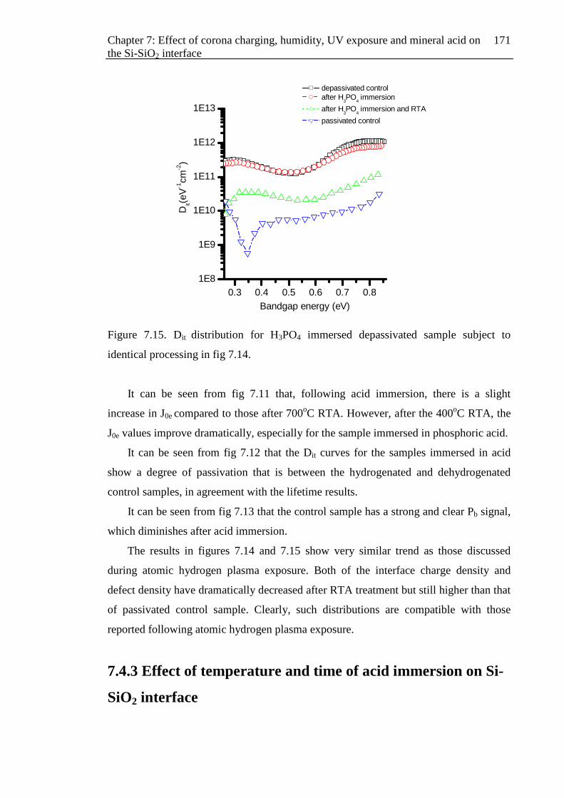
Chapter 7: Effect of corona charging, humidity, UV exposure and mineral acid on the Si-SiO2 interface
171
0.3 0.4 0.5 0.6 0.7 0.81E8
1E9
1E10
1E11
1E12
1E13
Dit(
eV-1cm
-2)
Bandgap energy (eV)
depassivated control after H
3PO
4 immersion
after H3PO
4 immersion and RTA
passivated control
Figure 7.15. Dit distribution for H3PO4 immersed depassivated sample subject to
identical processing in fig 7.14.
It can be seen from fig 7.11 that, following acid immersion, there is a slight
increase in J0e compared to those after 700oC RTA. However, after the 400oC RTA, the
J0e values improve dramatically, especially for the sample immersed in phosphoric acid.
It can be seen from fig 7.12 that the Dit curves for the samples immersed in acid
show a degree of passivation that is between the hydrogenated and dehydrogenated
control samples, in agreement with the lifetime results.
It can be seen from fig 7.13 that the control sample has a strong and clear Pb signal,
which diminishes after acid immersion.
The results in figures 7.14 and 7.15 show very similar trend as those discussed
during atomic hydrogen plasma exposure. Both of the interface charge density and
defect density have dramatically decreased after RTA treatment but still higher than that
of passivated control sample. Clearly, such distributions are compatible with those
reported following atomic hydrogen plasma exposure.
7.4.3 Effect of temperature and time of acid immersion on Si-
SiO2 interface

Chapter 7: Effect of corona charging, humidity, UV exposure and mineral acid on the Si-SiO2 interface
172
0 1 2 3 4
100
1000
J 0e (
fA/c
m2 )
RTA time (min)
5 mins 170oC H3PO
4
40 mins 170oC H3PO
4
16 hrs room temperature H3PO
4
control sample
(b)
0 1 2 3 4
2000
4000
6000
8000
10000
Effe
ctiv
e lif
etim
e (µ
s)
RTA time (min)
5 min 170oC H3PO
4
40 min 170oC H3PO
4
16 hrs room temperature H3PO
4
control sample
(a)
In this section, the effect of immersion temperature and time on the passivation of
Si-SiO2 interface is investigated. After acid immersion under different conditions,
samples received cumulatively RTA anneal until 4 minutes. Figure 7.16 and 7.17 show
H3PO4 and HCL immersed depassivated samples respectively. For comparison, a
depassivated control sample without any acid immersion also displayed in figure 7.16
and 7.17.
Figure 7.16. (a) Effective lifetime τ and (b) J0e for samples of initially H3PO4 immersed
at different times and temperatures as a function of RTA annealing time.

Chapter 7: Effect of corona charging, humidity, UV exposure and mineral acid on the Si-SiO2 interface
173
0 1 2 3 4
200
300
400
500
600
J 0e (
fA/c
m2 )
RTA time (min)
16 hr 60 oC HCL 16 hr room temperature HCL control sample
(b)
0 1 2 3 4400
800
1200
1600
2000
24002800
Effe
ctiv
e lif
etim
e (µ
s)
RTA time (min)
16 hr 60oC HCl 16 hr room temperature HCl control sample
(a)
Figure 7.17. (a) Effective lifetime τ and (b) J0e for samples of initially HCl immersed at
different temperatures as a function of RTA annealing time.
It can be seen from figures 7.16 and 7.17, it is the acid temperature rather than the
immersion time that plays a critical role in the passivation effect of mineral acids on the
Si-SiO2 interface. Even 5 minutes 170oC H3PO4 immersion can reach nearly equivalent
passivation effect to that received 40 minutes immersion sample.

Chapter 7: Effect of corona charging, humidity, UV exposure and mineral acid on the Si-SiO2 interface
174
The results for the different measurements clearly show that hydrogen or a hydrogen
complex is diffusing into the oxide layer during acid immersion of the samples, and
affecting the interface properties.
One possible explanation could be that the acid immersions result in the creation of
atomic hydrogen which then diffuses into the oxide. It has been shown that exposure of
the interface to atomic hydrogen results in the (incomplete) re-hydrogenation of existing
Si interface defects, but also in the generation additional, thermally unstable defects, as
has been observed previously for Si-SiO2 interfaces exposed to atomic hydrogen [25, 26,
39]. The slight increase in J0e following acid immersion could be the result of the
additional, thermally unstable but recombination active defects, which offset the effect
of the partial passivation of existing, thermally stable defects (chiefly Pbx centres). The
subsequent 400oC RTA is sufficient to remove these additional defects without a
significant loss of hydrogen from the interface, resulting in the observed Dit and Pb
centre density. However, the density of unpassivated defects reduction of J0e, as well as
the reduction in both passivated interface defects is not reduced to the level achieved by
the introduction of molecular hydrogen, through a forming gas anneal. Previous work
has shown that atomic hydrogen exposure is not as effective at defect passivation as
molecular hydrogen.
The fact that H3PO4 immersion results in more efficient re-hydrogenation than HCl
is probably a result of the higher temperature of the former, which leads to a faster
diffusion and may also result in the availability of a higher concentration of atomic
hydrogen in the solution. Differences in solution concentration and the chemical
properties of the acid may also play a role. In particular, the (slow) etching of the oxide
in H3PO4 (estimated reduction in oxide thickness after etching ~5nm) may play an
important role in the generation of atomic hydrogen.
7.5 Summary
The results show, on the one hand, corona charging is not necessarily a non-invasive
technique and there are some difference in the nature of defects introduced between
corona charging and atomic H exposure, and on the other hand, corona charging could
perhaps be used as a low cost means of atomic hydrogen generation. However, it is
necessary to continue to explore and find the optimum corona charging condition.

Chapter 7: Effect of corona charging, humidity, UV exposure and mineral acid on the Si-SiO2 interface
175
In addition, the results show that humidity and UV exposure will result in the
degradation of Si-SiO2 stack. The mechanism behind this is mainly due to the atomic
hydrogen existed in the oxide film. For humidity exposed samples, the general trend of
the interface modification, both after humidity exposure and subsequent thermal
annealing, was largely consistent with the effect of atomic hydrogen on the Si-SiO2
interface. For UV exposed samples, the general trend of the interface modification was
largely consistent with the hydrogen redistribution model in which the atomic H in the
oxide film released by hot electrons is mainly responsible for the change oft the Si-SiO2
interface.
Finally, the results show that the immersion of oxidised silicon samples in mineral
acids can result in a modification to the Si-SiO2 interface properties. Care therefore
needs to be taken when such treatments are employed for the preparation of samples for
characterisation. However, acid immersion could also provide a very cheap, alternative
means of surface passivation due to hydrogen or a hydrogen complex diffusing into the
oxide layer and affecting the interface properties.

Chapter 7: Effect of corona charging, humidity, UV exposure and mineral acid on the Si-SiO2 interface
176

Summary and further work 177
Summary and further work In summary, the work of this thesis has mainly focused on the effect of atomic
hydrogen on the Si-SiO2 interface. Firstly, the passivation effect of thin thermal oxides
grown at relatively low temperature (750-900oC), and of oxide/LPCVD nitride stacks
with a low temperature oxide was investigated. Secondly, the influence of plasma
atomic hydrogen on the surface passivation of the Si-SiO2 interface was investigated.
Finally, the degree of similarity of corona charging, humidity, UV exposure and mineral
acid, in terms of their effect on the Si-SiO2 interface properties compared to the effect of
atomic hydrogen, was studied. The main results can be summarized as follows:
For low temperature wet oxidations, firstly, a higher oxidation temperature results
in better surface passivation. A reasonable compromise may be a temperature of ~850oC.
Secondly, surface orientation has a large effect on achievable surface passivation. (111)
surfaces display high recombination rates even at an oxidation temperature of 850oC
and following an FGA. Thirdly, the diffusion of phosphorous into the oxide results in a
significant improvement in surface passivation due to a slight increase in positive
charge density. However, the surface passivation deteriorates markedly if the diffusion
reaches the interface.
On the other hand, for oxide/nitride stacks, firstly, a practical temperature for the
LPCVD nitride deposition may be in the range 750-775oC. Secondly, the thermal
stability of the surface passivation is much better than for samples with an oxide only,
due to the presence of hydrogen in the nitride which re-passivates interface defects.
Thirdly, even for oxide/nitride stacks, the passivation does not seem to be stable.
For the effect of atomic hydrogen on the Si-SiO2 interface, the atomic H exposure
results in the generation of additional defects at the Si-SiO2 interface. These defects are
efficient carrier recombination centres, are thermally unstable and can be effectively
removed by a short RTA anneal at 300oC or above. Even at lower temperature (240oC)
in air or N2, most thermally unstable defects can be removed for a sufficiently long
annealing time. The annealing of this thermally unstable defect is not characterized by a
single activation energy but rather by a spread of activations energies.
It is best to use MW plasma with low power and minimise exposure time to avoid
plasma damage and achieve a steady state. The degree of steady-state passivation shows
no discernible dependence on temperature in the range 25-600oC during atomic H
plasma exposure. In particular, at all sample temperatures in the range 25-600oC, the

Summary and further work 178
efficiency of defect passivation by H is lower than that afforded by H2. The presence of
a phosphorous diffusion layer does not fundamentally alter the physics of interface
passivation and the response to atomic hydrogen is insensitive to crystal orientation.
A sufficiently high electric field created by corona charging results in the
introduction of additional defects to the Si-SiO2 interface and these defects can be
subsequently removed by an RTA treatment, which are consistent with effects of atomic
hydrogen on the Si-SiO2 interface. Following identical low temperature anneal, both
corona charging and atomic hydrogen exposed samples show similar but not identical
improvement behaviour. This suggests that, while the underlying cause of the
degradation is likely to be the same in both cases (atomic H), there are some differences
in the generated defects, perhaps as a result of different H fluxes or other factors.
Humidity and UV exposure will result in the degradation of Si-SiO2 stack and there
is an improvement following thermal annealing. The general trend of the interface
modification is largely consistent with the effect of atomic hydrogen on the Si-SiO2
interface. The mechanism behind this is mainly due to the atomic hydrogen existing in
the oxide film.
Finally, our results show that immersion of oxidised silicon samples in mineral
acids can result in a modification to the Si-SiO2 interface properties. Care therefore
needs to be taken when such treatments are employed for the preparation of samples for
characterisation. However, acid immersion could also provide a very cheap, alternative
means of surface passivation due to hydrogen or a hydrogen complex diffusing into the
oxide layer and affecting the interface properties.
From the work of this thesis, some of further work is suggested as follows:
Determining the mean activation energy of atomic hydrogen induced defects In this thesis, the thermal annealing behaviour of defects introduced by atomic
hydrogen at the Si-SiO2 interface has been investigated. However, the experimental data
could so far not be fitted to models describing the annealing behaviour, and hence the
important parameters describing the annealing behaviour (activation energy and spread)
have not been determined. Modelling the results is complicated by the fact that J0e is not
only related to the defect density, but also to the charge density and the properties of the
interface defects. It seems warranted to achieve more accurate post-atomic hydrogen
exposure annealing results to calculate the mean activation energy of atomic hydrogen

Summary and further work 179
induced defects. This could be realized by measuring low temperature annealed samples
at ‘real’ room temperature (ensuring to accurately convert all J0e measurements to room
temperature equivalents) after sufficiently long time cooling TIDLS system (i.e. more
than 2 hours). Meanwhile, a ‘control’ lifetime sample could be used in measurements.
This ‘control’ sample should be a diffused sample with a good J0e and ideally with
silicon nitride on top, thus it is not susceptible to degradation due to humidity. J0e
measurements of this sample using TIDLS could be done every time when other
annealed samples are measured at room temperature. An accurate activation energy
value can direct our thermal annealing with an effective and economical measure.
UV stability of Si-SiO2 stacks and Si-SiO2-PECVD SiN stacks The results presented in this thesis suggest that the source of hydrogen which leads
to the UV degradation under an applied electric field is mainly the existing hydrogen in
the SiO2 film. More work on understanding the source of the hydrogen, and the impact
that the oxide growth conditions (dry/wet, with/without TCA) have on the rate and
magnitude of the degradation would be appropriate. Currently there is no clear picture
on these issues from the literature. Detailed investigation of stack structures, in
particular SiO2/PECVD SiNx stacks could be performed, since these are of greatest
practical interest. Therefore it is appropriate to investigate the influence of oxide
thickness (and oxide growth conditions) on both the rate and total extent of any
observed degradation. Silicon nitride layers usually contain a positive charge. The
results of Black and McIntosh [54] have shown that the presence of positive charge on
the surface of an oxide plays a key role in promoting degradation, and that this surface
charge is neutralised by electrons injected into and across the oxide. It would be worth
investigating whether a similar effect can be observed with respect to the positive
nitride charge.
Comparison of passivation effect on Si-SiO2-PECVD SiN stacks between H and H2 following high temperature thermal anneal The passivation effect on Si-SiO2 stacks between H and H2 has been investigated.
However, it is the Si-SiO2-PECVD SiNx stacks that attract more attention in
photovoltaic community. It would be worth to investigate the difference in passivation

Summary and further work 180
effectiveness on this kind of stacks between H and H2. This could be done by measuring
the appropriate quantities (Dit/J0e/S) at various stages of sample processing – after
thermal oxidation and FGA; after PECVD SiNx deposition; after a subsequent high
temperature treatment to release atomic H; and again after stripping the nitride layer and
re-hydrogenating the oxide with an FGA.

List of Publications 181
List of Publications
Publications arising from the work in this thesis
Refereed Journal papers
[1] C. Zhang, K. J. Weber, and H. Jin, “Passivation and Depassivation of Si-SiO2
Interfaces with Atomic Hydrogen,” Journal of Electrochemical Society, 156(11), H836,
(2009).
[2] H. Jin, W. E. Jellett, Z. Chun, K. J. Weber, A. W. Blakers, and P. J. Smith, “The
effect of boron diffusions on the defect density and recombination at the (111) silicon-
silicon oxide interface,” Applied Physics Letters, 92(12), 122109, (2008).
[3] H. Jin, K. J. Weber and C. Zhang, “Effect of Phosphorus Diffusion to the
Recombination at the Si–SiO2 Interface,” Progress in Photovoltaics: Research and
Applications, 17, 177, (2009).
Refereed conference publications:
[4]. C. Zhang, H. Jin, W. E. Jellett, and K. J. Weber, “The influence of corona
charging on the Si/SiO2 interface,” 23th European Photovoltaic Solar Energy
Conference, Valencia, Spain, 1-5, September, 2008.
[5]. C. Zhang, H. Jin, W. E. Jellett, P. J. Smith and K. J. Weber, “Hydrogen introduction
by acid solution to Si/SiO2 interface,” 23th European Photovoltaic Solar Energy
Conference, Valencia, Spain, 1-5, September, 2008.
[6]. H. Jin, W. Jellett, C. Zhang, and K. J. Weber, “Effect of Diffusions on Si surface
passivation,” 23th European Photovoltaic Solar Energy Conference, Valencia, Spain, 1-
5, September, 2008.
[7]. W. Jellett, C. Zhang, H. Jin, P. J. Smith and K. J. Weber, “Boron Emitters: Defects
at the Silicon-Silicon Dioxide interface,” 33th IEEE Photovoltaic Specialists
Conference, San Diego, California, United States, 11-16, May. 2008.
[8]. C. Zhang, K. J. Weber, and H. Jin, “Effect of atomic H exposure on thermally
oxidized Si/SiO2 interfaces,” 24th European Photovoltaic Solar Energy Conference,
Hamburg, Germany, 21-25, September, 2009.

List of Publications 182
[9]. C. Zhang, K. J. Weber, H. Jin and N. S. Zin, “The effect of exposure of Si-SiO2
structure to atomic H by PECVD reactor,” 34th IEEE Photovoltaic Specialists
Conference, Philadelphia, Pennsylvania, United States, 7-12, June, 2009.
[10]. H. Jin, K. J. Weber, C. Zhang and Y. Ren, “Low Si surface recombination through
negatively charged Si3N4 films,” 24th European Photovoltaic Solar Energy Conference,
Hamburg, Germany, 21-25, September, 2009.
[11]. K. J. Weber, H. Jin, C. Zhang, N. Nursam and W. Jellett, “Surface Passion Using
Dielectric Films: How Much Charge is Enough?” 24th European Photovoltaic Solar
Energy Conference, Hamburg, Germany, 21-25, September, 2009.
[12]. N. S. Zin, A. Blakers, K. J. Weber and C. Zhang “Investigation of Lifetime
Degradation of RIE-Processed Silicon Samples for Solar Cells,” 34th IEEE
Photovoltaic Specialists Conference, Philadelphia, Pennsylvania, United States, 7-12,
June, 2009.
[13]. H. Jin, K. J. Weber, B. B. Paudyal, and C. Zhang, “Introduction of Negative
Charges in Nitride for PV Applications,” 34th IEEE Photovoltaic Specialists
Conference, Philadelphia, Pennsylvania, United States, 7-12, June, 2009.
[14]. C. Zhang and K. J. Weber, “The thermal stability of atomic H plasma produced
interface defects on Si-SiO2 stack ,” 35th IEEE Photovoltaic Specialists Conference,
Honolulu, Hawaii, United States, 20-25, June, 2010.

Bibliography 183
Bibliography
[1]. A. G. Aberle, Crystalline Silicon Solar Cells: Advanced Surface Passivation and
Analysis, University of New South Wales, Sydney (1999). p.23-24
[2]. C. R. Helms and E. H. Poindexter, “The silicon-silicon-dioxide system: its
microstructure and imperfections,” Reports on Progress in Physics, 57 (8), 791, (1994).
[3]. A. G. Aberle, “Surface Passivation of Crystalline Silicon Solar Cells: A Review,”
Progress in Photovoltaics: Research and Applications, 8, 473, (2000).
[4]. A. G. Aberle and R. Hezel, “Progress in Low-temperature Surface Passivation of
Silicon Solar Cells using Remote-plasma Silicon Nitride,” Progress in Photovoltaics:
Research and Applications, 5, 29, (1997).
[5]. R. Hezel and R. Schorner, “Plasma Silicon nitride-A promising dielectric to achieve
high-quality silicon MIS/IL Solar Cells,” Journal of Applied Physics, 52(4), 3076,
(1981).
[6]. S. Narasimha and A. Rohatgi, “Effective passivation of the low resistivity silicon
surface by a rapid thermal oxide/plasma silicon nitride stack,” Applied Physics Letters,
72(5), 1872, (1998).
[7]. A. G. Aberle, Crystalline Silicon Solar Cells: Advanced Surface Passivation and
Analysis, University of New South Wales, Sydney (1999). p.103
[8]. B. Hoex, S. B. S. Heil, E. Langereis, M. C. M. van de Sanden, and W. M. M.
Kessels, “Ultralow surface recombination of c-Si substrate passivated by plasma-
assisted atomic layer deposited Al2O3,” Applied Physics Letters, 89(4), 042112, (2006).
[9]. M. Hofman, S. Kambor, C. Schmidt, D. Grambole, J. Rentsh, S. W. Glunz, and R.
Preu, “PECVD-ONO: A New Deposited Firing Stable Rear Surface Passivation Layer
System for Crystalline Silicon Solar Cells,” Advances in optoelectronics, 485467,
(2008).
[10]. A. Rohatgi, P. Doshi, J. Moschner, T. Lauinger, A. G. Aberle and D. S. Ruby,
“Comprehensive Study of Rapid, Low-Cost Silicon Surface Passivation Technologies,”
IEEE Transactions on Electron Devices, 47(5), 987, (2000).
[11]. S. R. Wenham, C. B. Honsberg, and M. A. Green, “Buried Contact Silicon Solar-
Cells,” Solar Energy Materials and Solar Cells, 34(1-4), 101, (1994).
[12]. F. H. P. M. Habraken, R. H. G. Tijhaar et al., “Hydrogen in low-pressure
chemical-vapor-deposited silicon (oxy)nitride films,” Journal of Applied Physics, 59(2),
447, (1986).

Bibliography 184
[13]. S. J. Pearton, J. W. Corbett, and T. S. Shi, “Hydrogen in Crystalline
Semiconductors,” Applied Physics A Solids and Surfaces, 43(3), 153-195 (1987).
[14]. J. I. Pankove, R. O. Wance, and J. E. Berkeyheiser, “Neutralization of acceptors in
silicon by atomic hydrogen,” Applied Physics Letters, 45(10), 1100, (1984).
[15]. T. Zundel and J. Weber, “Dissociation energies of shallow-acceptor-hydrogen
pairs in silicon,” Physical Review B, 39(18), 13549, (1989).
[16]. Z. Z. Chen, S. Peyman, S. Jalal, and A. Rohatgi, “A novel and effective PECVD
SiO2/SiN antireflection coating for Si solar cells,” IEEE Transactions on Electron
Devices, 40(6), 1161, (1993).
[17]. A. Ebong, P. Doshi, S. Narasimha, A. Rohatgi, J. Wang, and M. A. El-Sayed,
“The effect of low and high temperature anneals on the hydrogen content and
passivation of Si surface coated with SiO2 and SiN films,” J. Electrochemical Society,
146(5), 1921, (1999).
[18]. J. I. Pankove and N. M. Johnson, Hydrogen in semiconductors, 1991, San Diego,
Academic press
[19]. A. Stesmans, “Revision of H2 passivation of Pb interface defects in standard (111)
Si/SiO2,” Applied Physics Letters, 68(19), 2723, (1996).
[20]. A. Stesmans, “Passivation of Pb0 and Pb1 interface defects in thermal (100)
Si/SiO2 with molecular hydrogen,” Applied Physics Letters, 68(15), 2076, (1996).
[21]. A. Stesmans, “Comparative Analysis of The H2 passivation of interface defects at
the (100) Si/SiO2 interface using Electron Spin Resonance,” Solid State
Communications, 97(4), 255, (1996).
[22]. A. Stesmans and V. V. Afanas’eV, “Hydrogen-induced thermal interface
degradation in (111) Si/SiO2 revealed by electron-spin resonance,” Applied Physics
Letters, 72(18), 2271, (1998).
[23]. A. Stesmans, “Interaction of Pb defects at the (111) Si/SiO2 interface with
molecular hydrogen: Simultaneous action of passivation and dissociation,” Journal of
Applied Physics, 88(1), 489, (2000).
[24]. J. Zhao, A. Wang, P. P. Altermatt, S. R. Wenham, and M. A. Green, “24%
Efficient perl silicon cell: Recent improvements in high efficiency silicon cell research,”
Solar Energy Materials and Solar Cells, 41/42, 87, (1996).
[25]. E. Cartier, J. H. Stathis, and D. A. Buchanan, “Passivation and depassivation of
silicon dangling bonds at the Si/SiO2 interface by atomic hydrogen,” Applied Physics
Letters, 63(11), 1510, (1993).
Bibliography 185
[26]. H. Jin, K. J. Weber, and P. J. Smith, “Characterization of the Si-SiO2 interface
following room temperature ammonia plasma exposure,” J. Electrochemical Society,
154(6), H417, (2007).
[27]. R. N. Hall, “Kinetics of hydrogen-defect complex formation in Ge and Si,” 13th
International Conference Defects in Semiconductors, Coronado, USA, (1984).
[28]. G. Bambakidis, R. C. Bowman, Hydrogen in disordered and amorphous solids,
Plenum Press, New York (1986). p. 61
[29]. J. I. Pankove, M. A. Lampert, M. L. Tang, “Hydrogenation and dehydrogenation
of amorphous and crystalline silicon,” Applied Physics Letters, 32(7), 439, (1978).
[30]. N. M. Johnson, D. K. Biegelsen, M. D. Moyer, V. R. Deline, C. A. Evans Jr,
“Deuterium at the Si-SiO2 interface detected by secondary-ion mass spectrometry,”
Applied Physics Letters, 38(12), 995, (1981)
[31]. J. W. Corbett, S. N. Sahu, T. S. Shi, L. C. Snyder, “Atomic and molecular
hydrogen in the Si lattice,” Physics Letters A, 93(6), 303 (1983).
[32]. T. S. Shi, S. N. Sahu, J. W. Corbett, L. C. Snyder, “State and Behavior of
Hydrogen in Silicon Lattice,” Scientia Sinica, Series A: Mathematical, Physical,
Astronomical & Technical Sciences 27(1), 98, (1984).
[33]. V. A. Singh, C. Weigel, J. W. Corbett, L M. Roth, “Vibration and Electronic
Structure of Hydrogen-Related Defects in Silicon Calculated by the Extended Hueckel
Theroy,” Physica Status Solidi (B) Basic Research 81(2), 637, (1977).
[34]. J. A. Appelbaum, R. R. Hamann, T. H. Tasso, “Hydrogen chemisorption on Si: A
new type of chemisorptive bond,” Physical Review Letters, 39(23), 1487, (1977).
[35]. L. C. Snyder, J. W. Moskowitz, S. Topiol “Computations to model three-centre
bonds in hydrogenated amorphous silicon,” Physical Review B, 26(12), 6727, (1982).
[36]. K. L. Brower, “Kinetics of H2 passivation of Pb centers at the (111) Si-SiO2
interface,” Physical Review B, 38(14), 9657, (1988).
[37]. K. L. Brower, “Dissociation kinetics of hydrogen-passivated (111) Si-SiO2
interface defects,” Physical Review B. 42(6), 3444, (1990).
[38]. A. Stesmans and G. V. Gorp, “Maximum density of Pb centres at the (111) Si-SiO2
interface after vacuum anneal,” Applied Physics Letters, 57(25), 2663, (1990).
[39]. J. Schmidt, M. Kerr and A. Cuevas, “Surface passivation of silicon solar cells
using plasma-enhanced chemical-vapour-deposited SiN films and thin thermal
SiO2/plasma SiN stacks,” Semiconductor Science and Technology, 16(3), 164, (2001).
[40]. J. H. Stathis and E. Cartier, “Atomic hydrogen reactions with Pb centres at the
(100) Si-SiO2 interface,” Physical Review letters, 72(17), 2745 (1994).

Bibliography 186
[41]. E. Cartier and J. H. Stathis, “Atomic Hydrogen-Induced Degradation of the Si-
SiO2 Structure,” Microelectronic Engineering, 28, 3, (1995).
[42]. R. E. Stahlbush and E. Cartier, “Interface Defect Formation in MOSFETs by
Atomic Hydrogen Exposure,” IEEE Transactions on Nuclear Science, 41(6), 1844,
(1994).
[43]. R. E. Stahlbush, E. Cartier and D. A. Buchanan, “Anomalous positive charge
formation by atomic hydrogen exposure,” Microelectronic Engineering, 28, 15 (1995).
[44]. D. J. DiMaria and J. W. Stasiak, “Trap creation in silicon dioxide produced by hot
electrons,” Journal of Applied Physics, 65(6), 2342, (1989).
[45]. D. J. DiMaria, D. Arnold, and E. Cartier, “Impact ionization and positive charge
formation in silicon dioxide films on silicon,” Applied Physics Letters, 60(17), 2118,
(1992).
[46]. E. Cartier and J. H. Stathis, “Hot-electron induced passivation of silicon dangling
bonds at the Si (111)/SiO2 interface,” Applied Physics Letters, 69(1), 103 (1996).
[47]. W. L. Warren and P. M. Lenahan, “Electron spin resonance study of high field
stressing in meta-oxide-silicon device oxides,” Applied Physics Letters, 49(19), 1296
(1986).
[48]. P. M. Lenahan and P. V. Dressendorfor, “Hole traps and trivalent silicon centers in
metal-oxide-silicon devices,” Journal of Applied Physics, 55(10), 3495, (1984).
[49]. K. Blumenstock and R. Hezel, “Interface state generation in the Si-SiO2 system by
nonionizing UV irradiation,” Insulating Films on Semiconductors, Proceedings of the
international conference INFOS 85, Toulouse, France, 221, (1985).
[50]. P. E. Gruenbaum, R. R. King, and R. M. Swanson, “Photo injected hot-electron
damage in silicon point-contact solar cells,” Journal of Applied Physics, 66(12), 6110,
(1989).
[51]. L. Zhong and F. Shimura, “Interface traps creation by sub-band gap irradiation in
silicon dioxide on silicon without applied electric field,” Journal of Applied Physics,
79(5), 2509, (1996).
[52]. W. P. Lee and Y. L. Khong, “The Effect of ultraviolet irradiation on the minority
carrier recombination lifetime of oxidized silicon wafers,” Journal of Electrochemical
Society, 144(5), L103, (1997).
[53]. W. P. Lee, Y. L. Khong and W. S. Seow, “Modelling the ultraviolet irradiation
effect on the effective minority carrier recombination lifetime of silicon wafers,”
Journal of Applied Physics, 85(2), 994, (1999).

Bibliography 187
[54]. L. E. Black and K. R. McIntosh, “Defect generation at charge-passivated Si-SiO2
interfaces by ultraviolet light,” IEEE Transactions on Electron Devices, 57(8), 1996,
(2010).
[55]. A. Stesmans and V. V. Afanas’ev, “Thermally induced interface degradation in
(111) Si-SiO2 traced by electron spin resonance,” Physical Review B, 54(16), R11129,
(1996).
[56]. A. Stesmans and V. V. Afanas’ev, “Thermally induced interface degradation in
(100) and (111) Si/SiO2 analyzed by electron spin resonance,” Journal of Vacuum
Science and Technology B, 16(6), 3108, (1998).
[57]. A. G. Aberle, S. Glunz and W. Warta, “Impact of illumination level and oxide
parameters on Shockley-Read-Hall recombination at the Si-SiO2 interface,” Journal of
Applied Physics, 71(9), 4422, (1992).
[58]. S. Rein, Lifetime Spectroscopy-A method of defect characterization in silicon for
photovoltaic applications, 2005, Springer, Germany, p.32-33.
[59]. A. G. Aberle, Crystalline Silicon Solar Cells: Advanced Surface Passivation and
Analysis. 1999, Sydney: UNSW. p14-23
[60]. S. Rein, Lifetime Spectroscopy-A method of defect characterization in silicon for
photovoltaic applications, Springer, Germany, 2005, p.49-50.
[61]. M. J. Kerr, “Surface, Emitter and Bulk Recombination in Silicon and
Development of Silicon Nitride Passivated Solar Cells,” PhD thesis, The Australian
National University, (2002).
[62]. D. E. Kane and R.M. Swanson, “Measurement of the emitter saturation current by
a contactless photoconductivity decay method,” 18th IEEE photovoltaic specialist
conference, Las Vegas, 578, (1985).
[63]. W. E. Jellett and K. J. Weber, “Accurate measurement of extremely low surface
recombination velocities on charged, oxidized silicon surfaces using a simple metal-
oxide-semiconductor structure,” Applied Physics Letters, 90(4), 042104, (2007).
[64]. A. Cuevas, “The effect of emitter recombination on the effective lifetime of silicon
wafers,” Solar Energy Materials and Solar Cells, 57, 277, (1999).
[65]. A. Cuevas and D. Macdonald, “Measuring and interpreting the lifetime of silicon
wafers,” Solar Energy, 76, 255, (2004).
[66]. A. Rohatgi, M. M. Hilali, and K. Nakayashiki, “High-efficiency screen-printed
solar cell on edge-defined film-fed grown ribbon silicon through optimized rapid belt
co-firing of contacts and high-sheet-resistance emitter,” Applied Physics Letters, 84(17),
3409, (2004).
Bibliography 188
[67]. H. Jin, “Characterization of Silicon/Silicon Dioxide/LPCVD Silicon Nitride stacks
for Solar Cells application,” PhD thesis, The Australian National University, (2007).
[68]. S. C. Jain and R. Muralidharan, “Effect of emitter recombination on the open
circuit voltage decay of a junction diode,” Solid State Electronics, 24, 1147, (1981).
[69]. D. H. Macdonald, “Recombination and Trapping in Multicrystalline Silicon Solar
Cells,” PhD thesis, The Australian National University, (2001).
[70]. D. K. Schroder, Semiconductor Material and Device Characterization, John Wiley
& Sons, New York (1990).
[71]. H. Nagel, C. Berge and A. G. Aberle, “Generalized analysis of quasi-steady-state
and quasi-transient measurements of carrier lifetimes in silicon,” Journal Applied
Physics, 86(11), 6218, (1999).
[72]. S. Rein, Lifetime Spectroscopy-A method of defect characterization in silicon for
photovoltaic applications, 2005, Springer, Germany, p.62.
[73]. R. A. Sinton, Andres Cuevas, “Contactless determination of current-voltage
characteristics and minority-carrier lifetimes in semiconductors from quasi-steady-state
photoconductance data,” Applied Physics Letters, 69(17), 2510, (1996).
[74]. A. S. Grove, B. E. Deal, E. H. Snow and C. T. Sah, “Investigation of thermally
oxidised silicon surfaces using metal-oxide-semiconductor structures,” Solid State
Electronics, 8(2), 145, (1965).
[75]. J. L. Moll, “Variable capacitance with large capacity change,” Institute of Radio
Engineers, Wescon convention record, part 3, 32, (1959).
[76]. W. G. Pfann and C. G. B. Garrett, “Semiconductor Varactor Using Space-Charge
Layers,” Proceedings of the Institute of Radio Engineers, 47(11), 2011 (1959).
[77]. D. R. Frankl, “Some effects of material parameters on the design of surface space-
charge varactors,” Solid State Electronics, 2(1), 71, (1961).
[78]. R. Linder, “Semiconductor surface varactor,” Bell System Technical Journal, 41,
803, (1962).
[79]. J. R. Ligenza and W. G. Spitzer, “The mechanisms for silicon oxidation in steam
and oxygen,” Journal of Physics and Chemistry of Solids, 14(C), 131, (1960).
[80]. E. H. Nicollian and J. R. Brews, MOS Physics and Technology, Wiley, New, York,
1982
[81]. S. M. Sze and Kwok K. NG, Physics of Semiconductor devices, Wiley, New,
York, 2006
Bibliography 189
[82]. B. E. Deal, E. L. Mackenna, and P. L. Castro, “Characteristics of fast surface
states associated with SiO2-Si and Si3N4-SiO2-Si structures,” Journal of
Electrochemical Society, 116(7), 997, (1969).
[83]. L. M. Terman, “An investigation of Surface states as a Silicon/Silicon Dioxide
Interface Employing Metal-Oxide-Silicon Diodes,” Solid State Electronics, 5(5), 285,
(1962).
[84]. C. N. Berglund, “Surface states at steam-grown silicon-silicon interfaces,” IEEE
Trans and Electron Devices, 13, 701, (1966).
[85]. R. Castagne, A. Vapaille, “Description of the SiO2-Si interface properties by
means of very low frequency MOS capacitance measurements,” Surface Science, 28,
157, (1971).
[86]. B. E. Deal, “The Current Understanding of Charges in the Thermally Oxidized
Silicon Structure,” Journal of Electrochemical Society, 121(6), 198C, (1974).
[87]. B. E. Deal, “Standardized Terminology for Oxide Charges Associated with
Thermally Oxidized Silicon,” IEEE Trans and electron devices, 27, 606, (1980).
[88]. Y. Nishi, “Study of Silicon-Silicon Dioxide Structure by Electron Spin
Resonance,” Japanese Journal of Applied Physics, 10(1), 52, (1971).
[89]. F. J. Caplan, E. H. Poindexter, B. E. Deal and R. R. Razouk, “ESR centers,
interface states, and oxide fixed charge in thermally oxidized silicon wafers,” Journal of
Applied Physics, 50(9), 5847, (1979).
[90]. J. A. Weil, “A review of electron spin spectroscopy and its application to the study
of paramagnetic defects in crystalline quartz,” Physics and Chemistry of Minerals, 10,
149, (1984).
[91]. D. L. Griscom, “Optical properties and structure of defects in silica glasss: optical
materials,” Journal of the Ceramic Society of Japan, 99, 923, (1991).
[92]. E. H. Poindexter, F. J. Caplan, and G. J. Gerardi, The physics and chemistry of
SiO2 and the Si-SiO2 interface, ed C. R Helms and B. E. Deal, 1988, New York: Plenum,
p.299
[93]. W. L. Warren, E. H. Poindexter, M. Offenberg, and W. Müller-Warmuth,
“Paramagnetic Point Defects in Amorphous Silicon Dioxide and Amorphous Silicon
Nitride Thin Films,” Journal of Electrochemical Society, 139(3), 872, (1992).
[94]. A. G. Revesz, B. Goldstein, “Electron paramagnetic resonance investigation of the
Si-SiO2 interface,” Surface Science, 14, 361, (1969).
[95]. K. L. Brower, “Electron paramagnetic resonance studies of Si-SiO2 interface
defects,” Semiconductor Science and Technology, 4(12), 970 (1989).

Bibliography 190
[96]. W. L. Hansen, S. J. Pearton, E. E. Hailer, “Bulk acceptor compensation produced
in p-type silicon at near-ambient temperatures by a H2O plasma,” Applied Physics
Letters, 44(6), 606 (1984).
[97]. J. E. Curran, “The properties and applications of low energy plasmas,” Vacuum
34(3-4), 343, (1984).
[98]. H. V. Boenig: Plasma Science and Technology, Cornell University Press, Ithaka,
NY (1983), p.36
[99]. G. S. Oehrlein, J. L. Lindstr6m, J. W. Corbett, “Electrolytical method for
hydrogenation of silicon,” Physics Letters, A, 81(4), 246, (1981).
[100]. S. J. Pearton, W. L. Hansen, E. E. Hailer, J. M. Kahn, “Hydrogenation of gold-
related levels in silicon by electronic doping,” Journal of Applied Physics, 55(4), 1221,
(1984).
[101]. S. J. Pearton, J. M. Kahn, E.E. Hailer, “Deep level effects in silicon and
germanium after plasma hydrogenation,” Journal of Electronic and Materials, 12(6),
1003, (1983).
[102]. T. C. Kho, K. R. McIntosh, J. T. Tan, A. F. Thomson, and F. W. Chen, “Removal
of hydrogen and deposition of surface charge during rapid thermal annealing ,” 33th
IEEE photovoltaic specialist conference, San Diego, CA, 978, (2008).
[103]. B. Rau, T. Weber, B. Gorka, P. Dogan, F. Fenske, K. Y. Lee, S. Gall, B. Rech,
“Development of a rapid thermal annealing process for polycrystalline silicon thin-film
solar cells on glass,” Materials Science and Engineering B 159-160, 329, (2009).
[104]. M. L. Terry, D. Inns, and A. G. Aberle, “Rapid Thermal Annealing and
Hydrogen Passivation of Polycrystalline Silicon Thin-Film Solar Cells on Low-
Temperature Glass,” Advances in OptoElectronics, 83657, (2007).
[105]. M. D. Yang, Y. K. Liu, J. L. Shen, and C. H. Wu, “Improvement of Material
Quality of Multijunction Solar Cells by Rapid Thermal Annealing,” Japanese Journal of
Applied Physics, 47(6), 4499, (2008).
[106]. P. K. Hurley, A. Stesmans, V. V. Afanas’ev, B. J. O’Sullivan and E. O’Callaghan,
“Analysis of Pb centers at the Si(111)/SiO2 interface following rapid thermal
annealing,” Journal of Applied Physics, 93(7), 3971, (2003).
[107]. S. Rein, Lifetime Spectroscopy-A method of defect characterization in silicon for
photovoltaic applications, 2005, Springer, Germany, p.231.
[108]. B. B. Paudyal, K. R. McIntosh, D. H. Macdonald, B. S. Richards and R. A.
Sinton, “The Implementation of Temperature Control to an Inductive-Coil
Bibliography 191
Photoconductance Instrument for the Range of 0–230oC,” Progress in Photovoltaics:
Research and Applications, 16, 609, (2008).
[109]. Z. Chen, S. K. Pang, K. Yasutake, and A. Rohatgi, “Plasma-enhanced chemical-
vapor-deposited oxide for low surface recombination velocity and high effective
lifetime in silicon,” Journal of Applied Physics, 74(4), 2856, (1993).
[110]. J. Sritharathikhun, C. Banerjee, M. Otsubo, T. Sugiura, H. Yamamoto, T. Sato, A.
Limmanee, A. Yamada, and M. Konagai, “Surface passivation of crystalline and
polycrystalline silicon using hydrogenated amorphous silicon oxide film,” Japanese
Journal of Applied Physics, 46(6A), 3296, (2007)
[111]. Z. Chen, K. Yasutake, A. Doolittle, and A. Rohatgi, “Record low SiO2/Si
interface state density for low temperature oxides prepared by direct plasma-enhanced
chemical vapor deposition,” Applied Physics Letters, 63(15), 2117, (1993).
[112]. B. E. Deal, M. Sklar, A. S. Grove, and E. H. Snow, “Characteristics of the
surface-state charge of thermally oxidized silicon,” J. Electrochemical Society, 114(3),
266, (1967)
[113]. M. J. McCann, K. J. Weber, and A. W. Blakers, “Surface passivation by
rehydrogenation of silicon-nitride-coated silicon wafers,” Progress in Photovoltaics:
Research and Applications, 13, 195, (2005).
[114]. H. Jin and K. J. Weber, “The effect of LPCVD silicon nitride deposition on the
Si-SiO2 interface of oxidized silicon wafers,” Journal of Electrochemical Society,
154(1), H5, (2007)
[115]. T. Lauinger, J. Moschner, A. G. Aberle, and R. Hezel, “Optimization and
characterization of remote plasma-enhanced chemical vapor deposition silicon nitride
for the passivation of p-type crystalline silicon surfaces,” Journal of Vacuum Science
and Technology A: Vacuum and Surfaces and Films, 16(2), 530, (1998).
[116]. E. Yablonovitch and T. J. Gmitter, “A contactless of minority lifetime probe of
heterostructure, surfaces, interfaces and bulk wafers,” Solid State Electronics, 35(3),
261, (1992).
[117]. S. W. Glunz, D. Biro, S. Rein, and W. Watra, “Field-effect passivation of the
SiO2-Si interface,” Journal of Applied Physics, 86(1), 683, (1999).
[118]. P. K. Hurley, B. J. O’Sullivan, F. N. Cubaynes, P. A. Stolk, F. P. Widdershoven,
and J. H. Das, “Examination of the Si(111)-SiO2, Si(110)-SiO2, and Si(100)-SiO2
Interfacial Properties Following Rapid Thermal Annealing,” Journal of Electrochemical
Society, 149(3), G194, (2002).

Bibliography 192
[119]. R. E. Stahlbush, E. Cartier and D. A. Buchanan, “Anomalous positive charge
formation by atomic hydrogen exposure,” Microelectronic Engineering, 28, 15, (1995)
[120]. S. Ponce-Alcaintara, C. del Canizo, J. Hofstetter and A. Luque, “The Effect of
RF and MW power on The SiNX films grown by PECVD,” IEEE Electron Devices,
Spanish Conference, 33, (2007).
[121]. A. G. Aberle, Crystalline Silicon Solar Cells: Advanced Surface Passivation and
Analysis. 1999, Sydney: UNSW. p94
[122]. K. R. McIntosh and L. P. Johnson, “Recombination at textured silicon surfaces
passivated with silicon dioxide,” Journal of Applied Physics, 105(12), 124520, (2009).
[123]. K. J. Weber, A. W. Blakers, M. J. Stocks, J. H. Babaei, V. A. Everett, A. J.
Neuendorf, and P. J. Verlinden, “A Novel Low-Cost, High-Efficiency Micromachined
Silicon Solar Cell,” IEEE Electron Device Letters, 25, 37, (2004).
[124]. H. Jin, K. J. Weber, and P. J. Smith, “Defect generation at SiO2/Si interfaces by
low pressure chemical vapour deposition of silicon nitride,” Applied Physics Letters,
89(9), 092120, (2006).
[125]. H. Jin, K. J. Weber and A. W. Blakers, “Hydrogen passivation of LPCVD
Si3N4/SiO2/Si stacks by ammonia plasma treatment,” Journal of Electrochemical
Society, 154(6) H430, (2007).
[126]. C. Zhang, K. J. Weber, and H. Jin, “Passivation and Depassivation of Si-SiO2
Interfaces with Atomic Hydrogen,” Journal of Electrochemical Society, 156(11), H836,
(2009).
[127]. H. Jin, K. J. Weber, N. C. Dang, and W. E. Jellett, “Defect generation at the Si-
SiO2 interface following corona charging,” Applied Physics Letters, 90(26), 262109,
(2007).
[128]. B. Hoex, S. B. S. Heil, E. Langereis, M. C. M. van de Sanden, and W. M. M.
Kessels “Ultralow surface recombination of c-Si substrates passivated by plasma-
assisted atomic layer deposited Al2O3,” Applied Physics Letters, 89(4), 042112, (2006).
[129]. M. M. Shahin, “Mass-spectrometric studies of corona discharges in air at
atmospheric pressures,” Journal of Chemical Physics, 45(7), 2600, (1966).
[130]. M. M. Shahin, “Use of corona discharges for the study of ion-molecular
reactions,” Journal of Chemical Physics, 47(11), 4392, (1967).
[131]. C. Zhang, H. Jin, W. E. Jellett, and K. J. Weber, “The influence of corona
charging on the Si/SiO2 interface,” 23th European Photovoltaic Solar Energy
Conference, 1-5 September 2008, Valencia, Spain, p.261

Bibliography 193
[132]. M. W. DeGroot, P. R. Elowe, J. Wilbur, J. George, and R. Feist, “High
throughput methodology for evaluation of the moisture barrier performance of thin
films for PV applications,” 34th IEEE Photovoltaic Specialists Conference, Philadelphia,
Pennsylvania, United States, 7-12, June, 2009, p.450
[133]. L. Lancellotti, R. Fucci, A. Romano, A. Sarno, and S. Daliento, “Induced
degradation on c-Si solar cells for concentration terrestrial applications,”
Microelectronics Reliability, 50, 1903, (2010).

Bibliography 194