Embed Size (px)
Citation preview
Integer-N and Fractional-N Synthesizers
Behzad RazaviElectrical Engineering Department
University of California, Los Angeles
Outline
General Synthesizer RequirementsInteger-N Synthesizers Basic Fractional-N SynthesizerRandomization and Noise Shaping
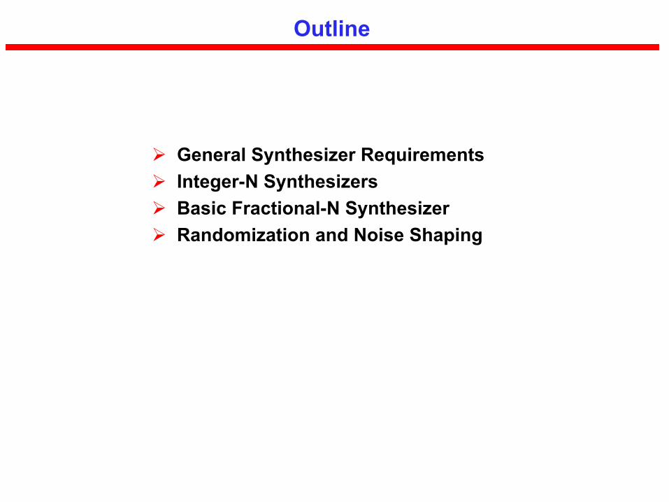
General Considerations
Channel SpacingFrequency AccuracyPhase NoiseSidebands (Spurs)Lock TimePower Dissipation
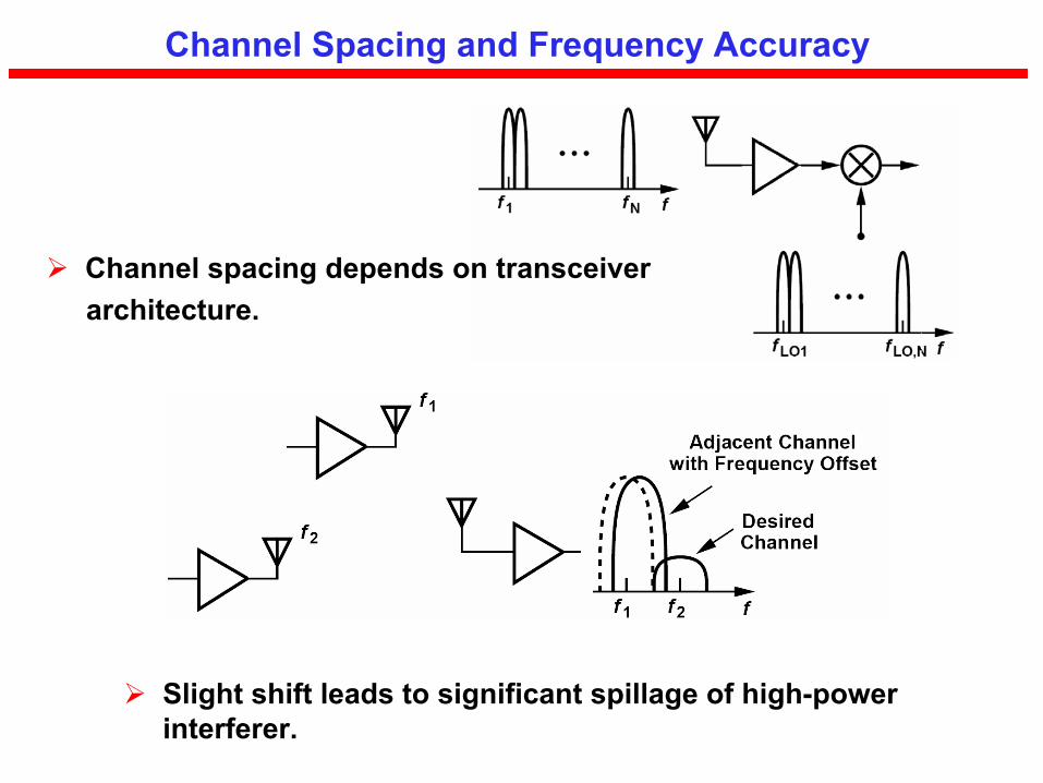
Channel Spacing and Frequency Accuracy
Slight shift leads to significant spillage of high-power interferer.
Channel spacing depends on transceiverarchitecture.
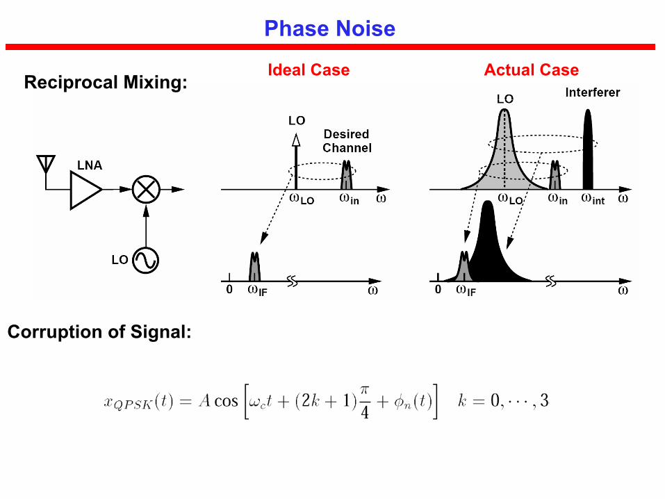
Phase Noise
Reciprocal Mixing:
Corruption of Signal:
Ideal Case Actual Case
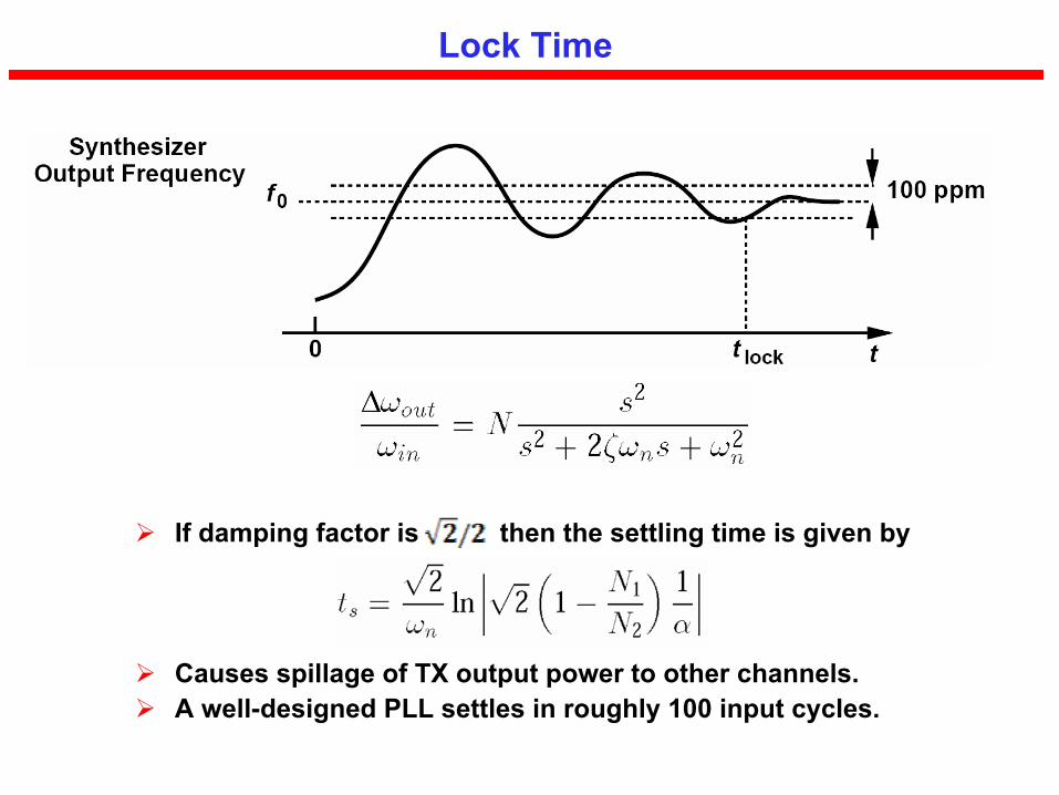
Lock Time
If damping factor is then the settling time is given by
Causes spillage of TX output power to other channels.A well-designed PLL settles in roughly 100 input cycles.
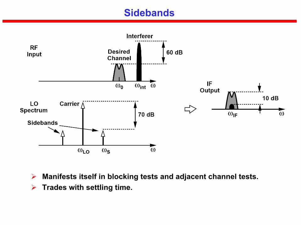
Sidebands
Manifests itself in blocking tests and adjacent channel tests.Trades with settling time.
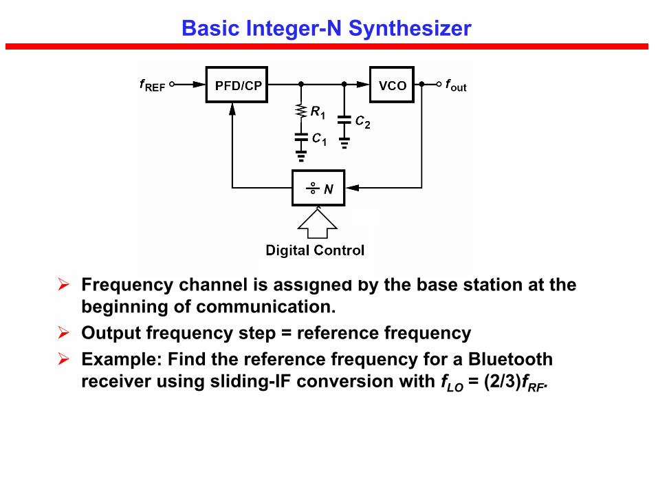
Basic Integer-N Synthesizer
Frequency channel is assigned by the base station at the beginning of communication.Output frequency step = reference frequencyExample: Find the reference frequency for a Bluetooth receiver using sliding-IF conversion with fLO = (2/3)fRF.
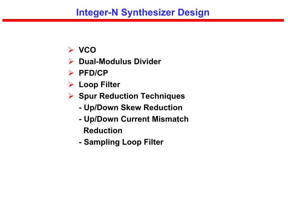
Integer-N Synthesizer Design
VCODual-Modulus DividerPFD/CPLoop FilterSpur Reduction Techniques- Up/Down Skew Reduction- Up/Down Current Mismatch Reduction
- Sampling Loop Filter
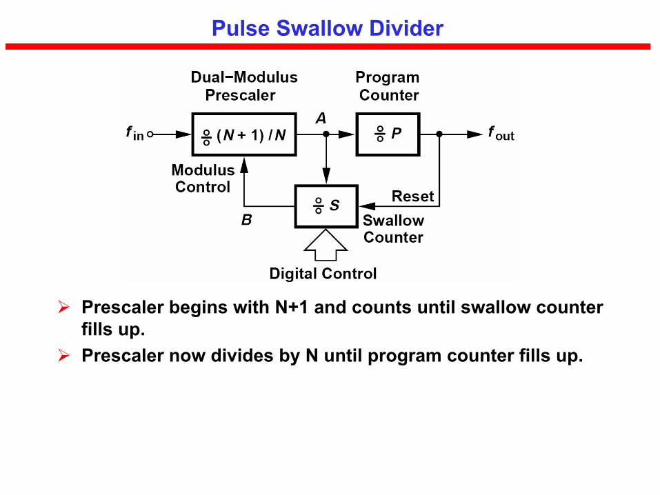
Pulse Swallow Divider
Prescaler begins with N+1 and counts until swallow counter fills up.Prescaler now divides by N until program counter fills up.
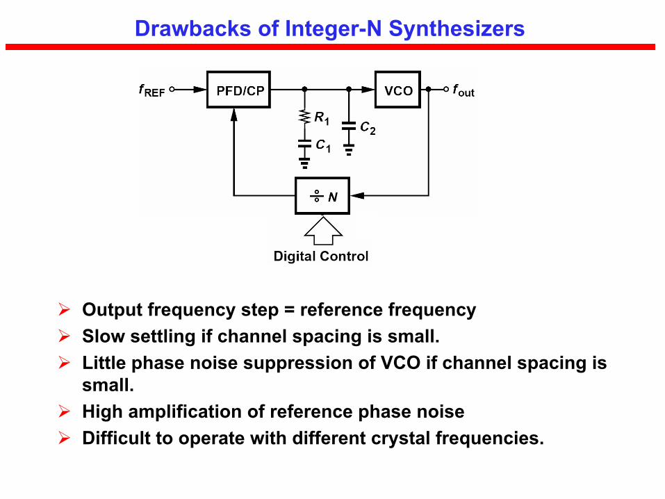
Drawbacks of Integer-N Synthesizers
Output frequency step = reference frequency Slow settling if channel spacing is small.Little phase noise suppression of VCO if channel spacing is small.High amplification of reference phase noiseDifficult to operate with different crystal frequencies.
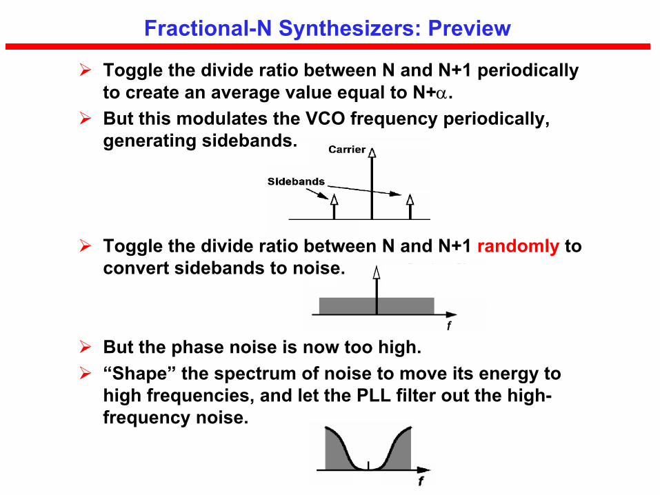
Fractional-N Synthesizers: Preview
Toggle the divide ratio between N and N+1 periodically to create an average value equal to N+α.But this modulates the VCO frequency periodically, generating sidebands.
Toggle the divide ratio between N and N+1 randomly to convert sidebands to noise.
But the phase noise is now too high.“Shape” the spectrum of noise to move its energy to high frequencies, and let the PLL filter out the high-frequency noise.
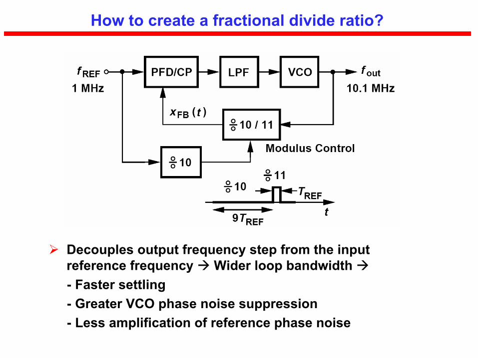
How to create a fractional divide ratio?
Decouples output frequency step from the input reference frequency Wider loop bandwidth - Faster settling- Greater VCO phase noise suppression - Less amplification of reference phase noise
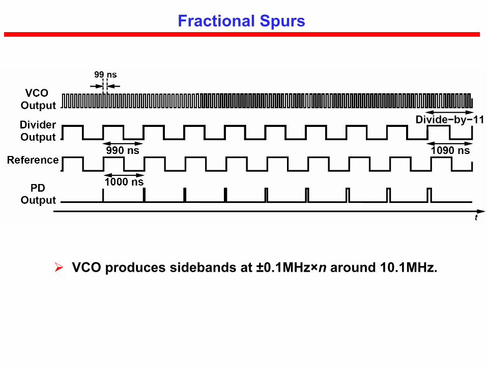
Fractional Spurs
VCO produces sidebands at ±0.1MHz×n around 10.1MHz.
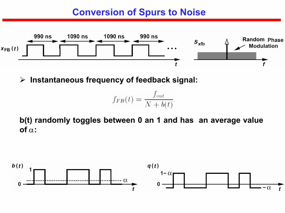
Conversion of Spurs to Noise
Instantaneous frequency of feedback signal:
b(t) randomly toggles between 0 an 1 and has an average value of α:
Random
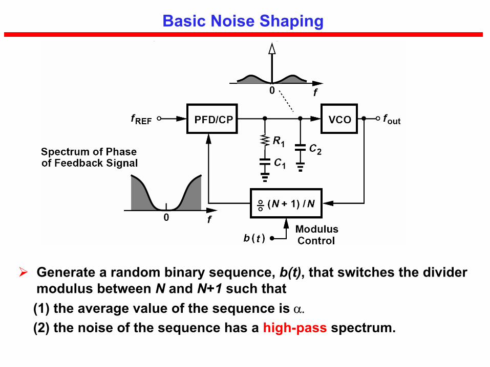
Basic Noise Shaping
Generate a random binary sequence, b(t), that switches the divider modulus between N and N+1 such that (1) the average value of the sequence is α.(2) the noise of the sequence has a high-pass spectrum.
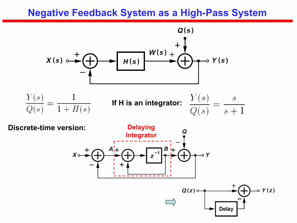
Negative Feedback System as a High-Pass System
Discrete-time version:
If H is an integrator:
DelayingIntegrator
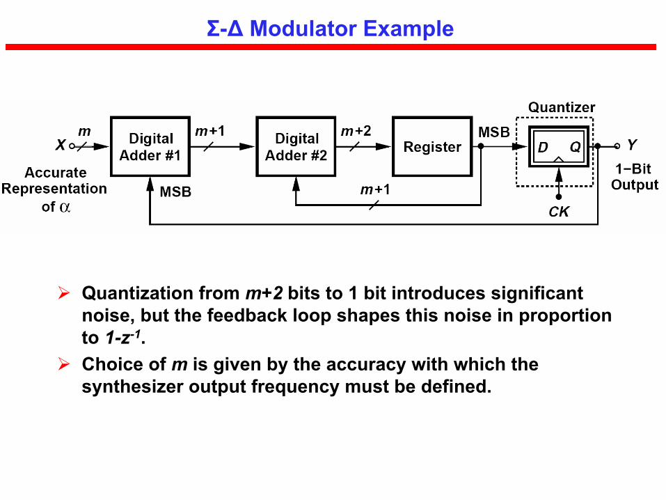
Σ-∆ Modulator Example
Quantization from m+2 bits to 1 bit introduces significant noise, but the feedback loop shapes this noise in proportion to 1-z-1. Choice of m is given by the accuracy with which the synthesizer output frequency must be defined.
19
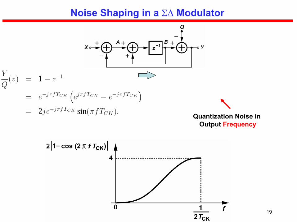
Noise Shaping in a Σ∆ Modulator
Quantization Noise in Output Frequency
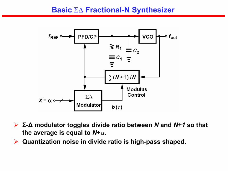
Basic Σ∆ Fractional-N Synthesizer
Σ-∆ modulator toggles divide ratio between N and N+1 so that the average is equal to N+α.Quantization noise in divide ratio is high-pass shaped.
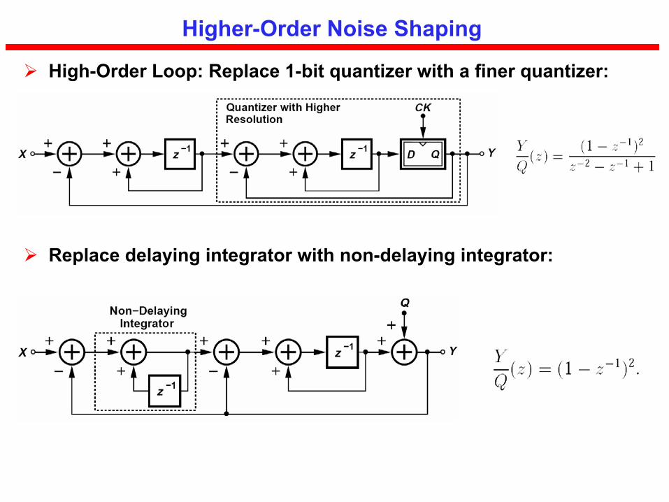
Higher-Order Noise Shaping
High-Order Loop: Replace 1-bit quantizer with a finer quantizer:
Replace delaying integrator with non-delaying integrator:
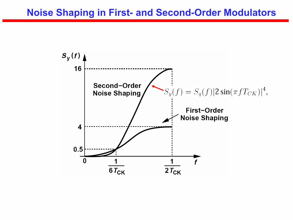
Noise Shaping in First- and Second-Order Modulators
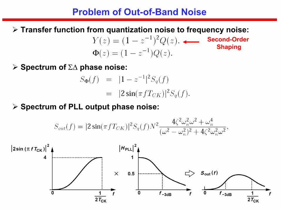
Problem of Out-of-Band Noise
Transfer function from quantization noise to frequency noise:
Spectrum of Σ∆ phase noise:
Spectrum of PLL output phase noise:
Second-Order Shaping
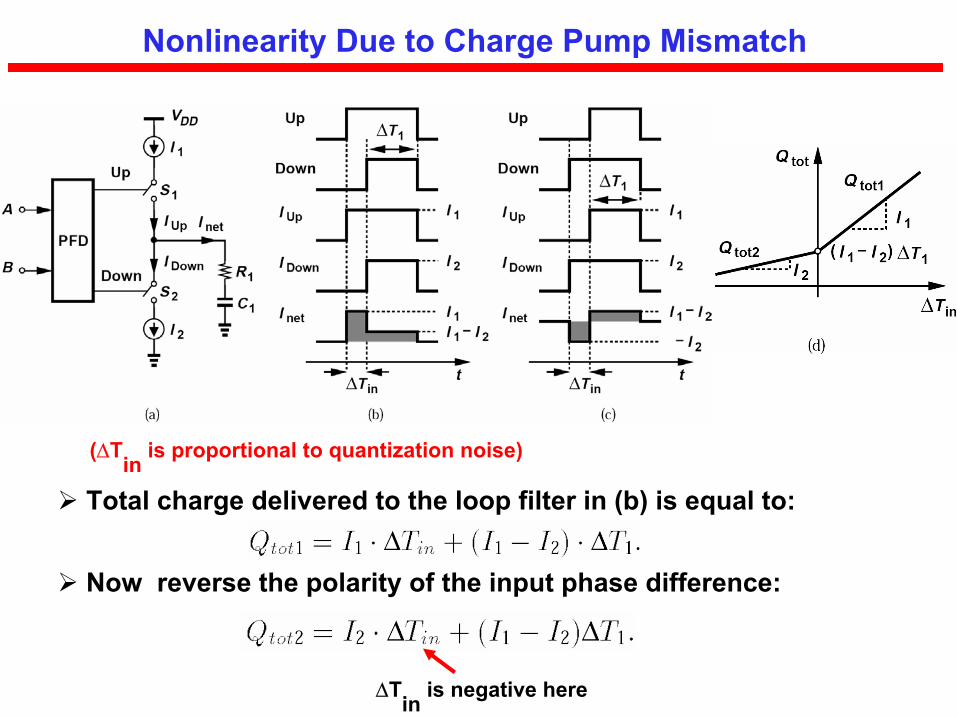
Nonlinearity Due to Charge Pump Mismatch
Total charge delivered to the loop filter in (b) is equal to:
Now reverse the polarity of the input phase difference:
∆Tin is negative here
(∆Tin is proportional to quantization noise)
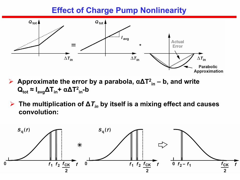
Effect of Charge Pump Nonlinearity
The multiplication of ∆Tin by itself is a mixing effect and causes convolution:
Approximate the error by a parabola, α∆T2in – b, and write
Qtot ≈ Iavg∆Tin+ α∆T2in-b
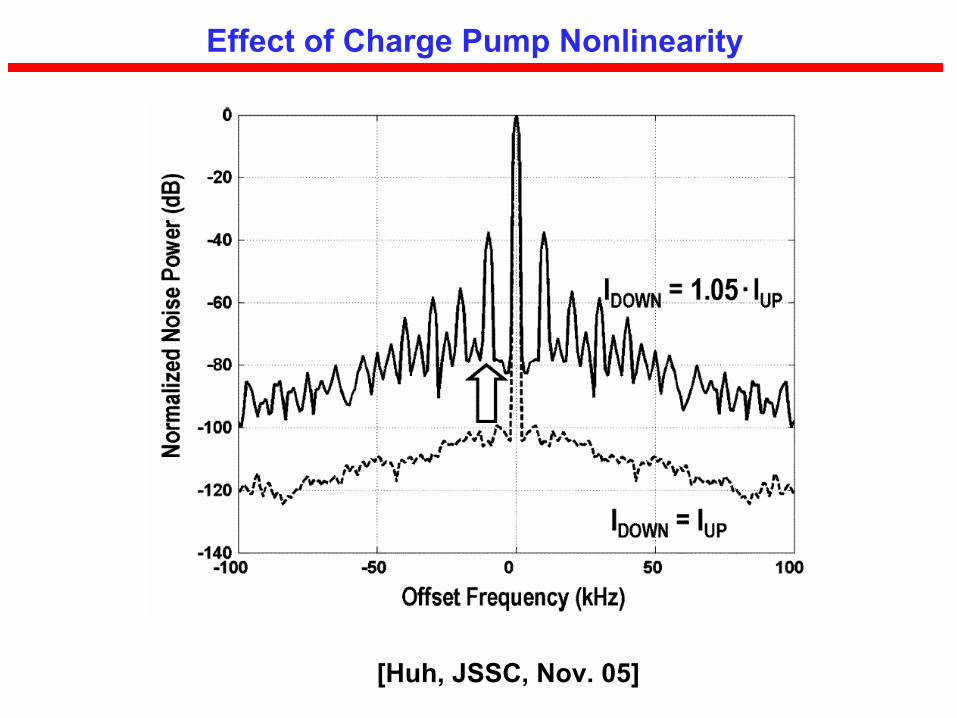
Effect of Charge Pump Nonlinearity
[Huh, JSSC, Nov. 05]


![[TI] Fractional Integer-N PLL Basics](https://img.pdfslide.us/doc/110x75/551447824a7959d2028b4f3d/ti-fractional-integer-n-pll-basics.jpg)