Embed Size (px)
Citation preview
Design and Analysis of Fractional-N Frequency Synthesizers
For Wireless Communications
Alaa Hussein
2
Outline
Motivation
Background
Novel Fractional-N Frequency Synthesizers
Novel Analog-to-Digital Architecture
Conclusions
3
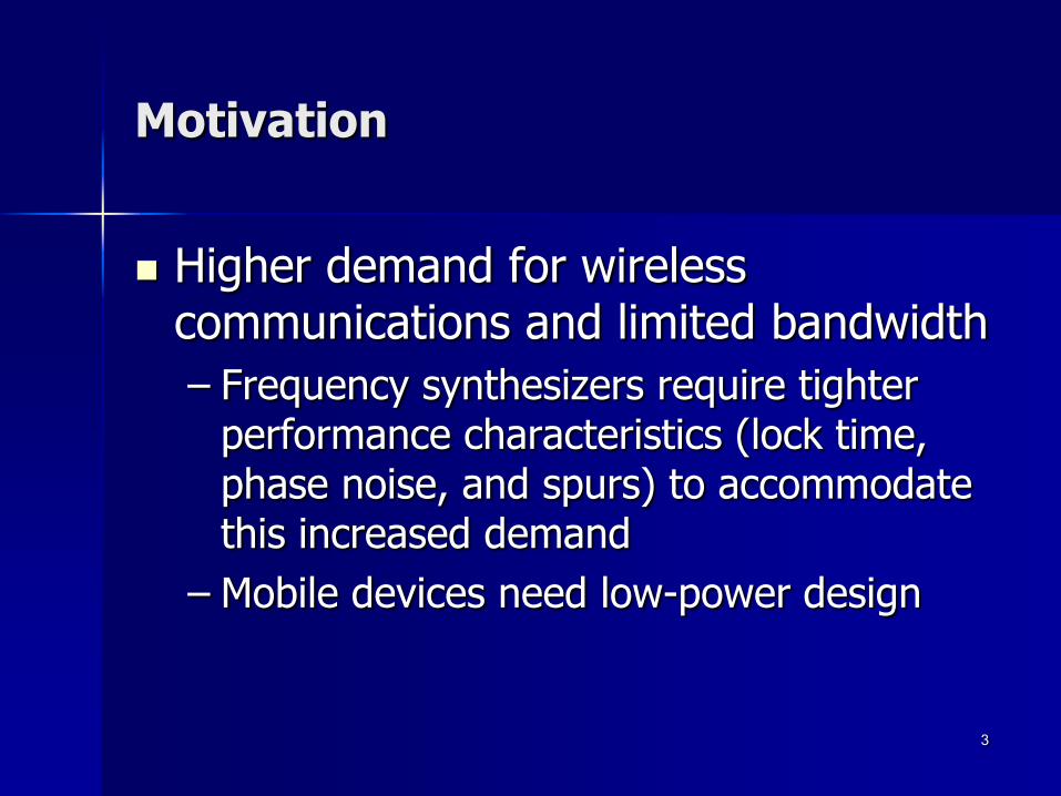
Motivation
Higher demand for wireless communications and limited bandwidth
– Frequency synthesizers require tighter performance characteristics (lock time, phase noise, and spurs) to accommodate this increased demand
– Mobile devices need low-power design
4
Outline
Motivation
Background
Novel Fractional-N Frequency Synthesizers
Novel Analog-to-Digital Architecture
Conclusions
5
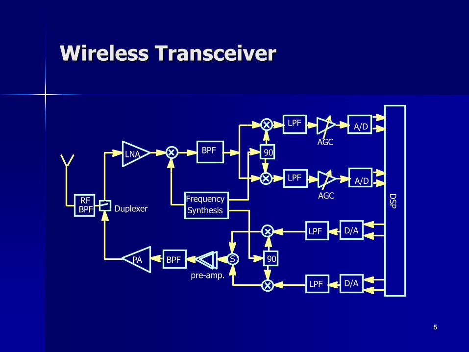
Wireless Transceiver
90
DSP
LNA
Duplexer
90
LPF D/A
LPF D/A
PA BPF
pre-amp.
BPF
RFBPF
Frequency
Synthesis
A/D
AGC
LPF
A/D
AGC
LPF
S
6
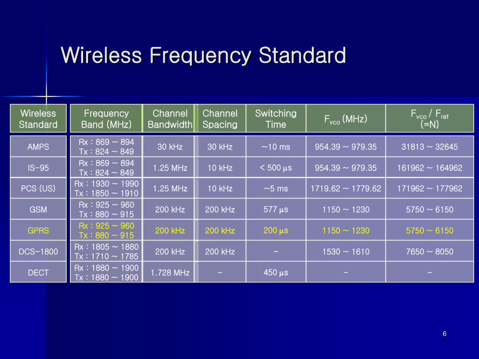
Wireless Frequency Standard
AMPS
IS-95
Rx : 869 ~ 894Tx : 824 ~ 849
30 kHz
Rx : 869 ~ 894Tx : 824 ~ 849
1.25 MHz
PCS (US)
GSM
Rx : 1930 ~ 1990Tx : 1850 ~ 1910
1.25 MHz
Rx : 925 ~ 960Tx : 880 ~ 915
200 kHz
30 kHz
10 kHz
10 kHz
200 kHz
~10 ms
< 500 ms
~5 ms
577 ms
954.39 ~ 979.35
954.39 ~ 979.35
1719.62 ~ 1779.62
1150 ~ 1230
31813 ~ 32645
161962 ~ 164962
171962 ~ 177962
5750 ~ 6150
WirelessStandard
FrequencyBand (MHz)
ChannelBandwidth
ChannelSpacing
SwitchingTime
Fvco (MHz)Fvco / Fref
(=N)
GPRSRx : 925 ~ 960Tx : 880 ~ 915
200 kHz 200 kHz 200 ms 1150 ~ 1230 5750 ~ 6150
DCS-1800Rx : 1805 ~ 1880Tx : 1710 ~ 1785
200 kHz 200 kHz - 1530 ~ 1610 7650 ~ 8050
DECTRx : 1880 ~ 1900Tx : 1880 ~ 1900
1.728 MHz - 450 ms - -
7
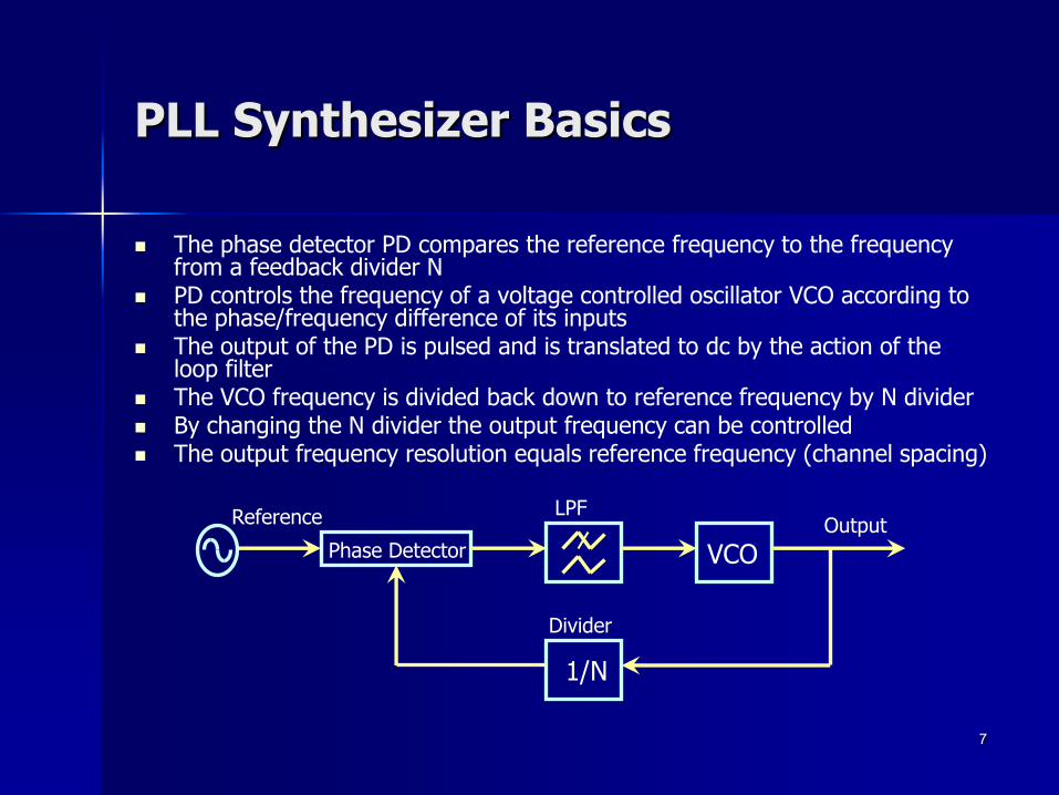
PLL Synthesizer Basics
The phase detector PD compares the reference frequency to the frequency from a feedback divider N
PD controls the frequency of a voltage controlled oscillator VCO according to the phase/frequency difference of its inputs
The output of the PD is pulsed and is translated to dc by the action of the loop filter
The VCO frequency is divided back down to reference frequency by N divider By changing the N divider the output frequency can be controlled The output frequency resolution equals reference frequency (channel spacing)
Phase Detector VCO
1/N
OutputReference
Divider
LPF
8
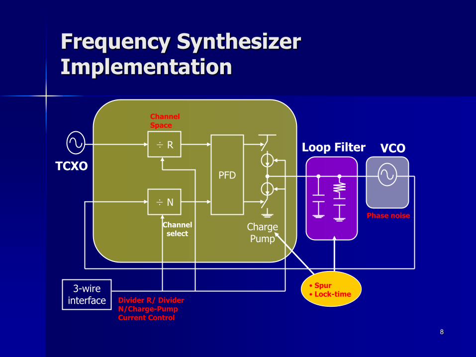
Frequency Synthesizer Implementation
÷ N
PFD
÷ R
TCXO
VCOLoop Filter
ChargePump
3-wireinterface
ChannelSpace
Channelselect
Divider R/ Divider N/Charge-Pump Current Control
Phase noise
• Spur• Lock-time
9
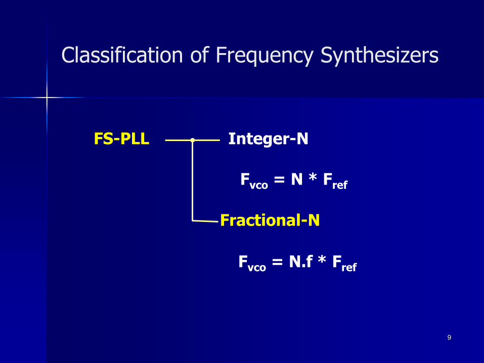
Classification of Frequency Synthesizers
FS-PLL Integer-N
Fvco = N * Fref
Fractional-N
Fvco = N.f * Fref
10
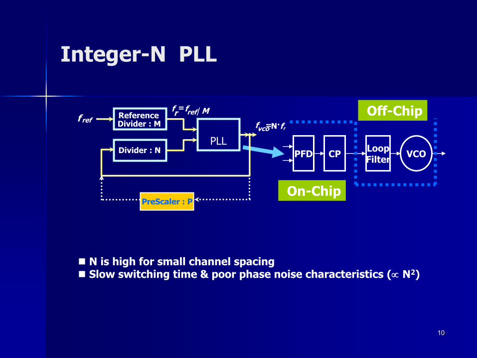
Integer-N PLL
N is high for small channel spacing Slow switching time & poor phase noise characteristics ( N2)
PFD CPLoopFilter
VCO
Off-Chip
On-Chip
rf·N
PLL
ReferenceDivider : M
Divider : N
reffMff refr
=
vcof =
PreScaler : P
11
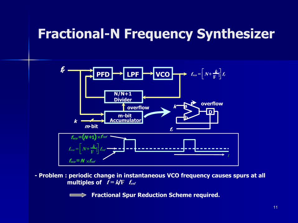
- Problem : periodic change in instantaneous VCO frequency causes spurs at all multiples of
Fractional-N Frequency Synthesizer
reffkf F=
PFD
N/N+1Divider
rf
m-bitAccumulatork
bit-m
overflow
rvco fk
Nf
+=FLPF VCO
Db
akoverflow
rf
refvco fk
Nf
+=F
refvco fNf ×=
( ) refvco fNf ×+= 1
Fractional Spur Reduction Scheme required.
t
12
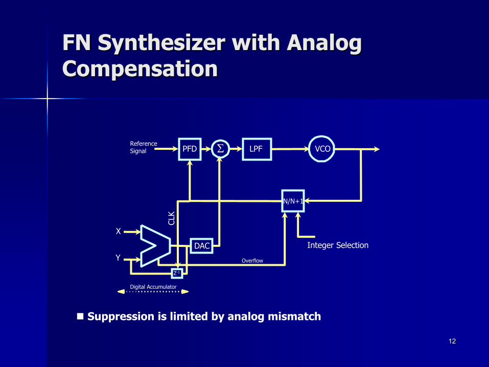
FN Synthesizer with Analog Compensation
ReferenceSignal PFD S LPF VCO
N/N+1
DAC
Z-1
CLK
Overflow
Integer Selection
X
Y
Digital Accumulator
Suppression is limited by analog mismatch
13
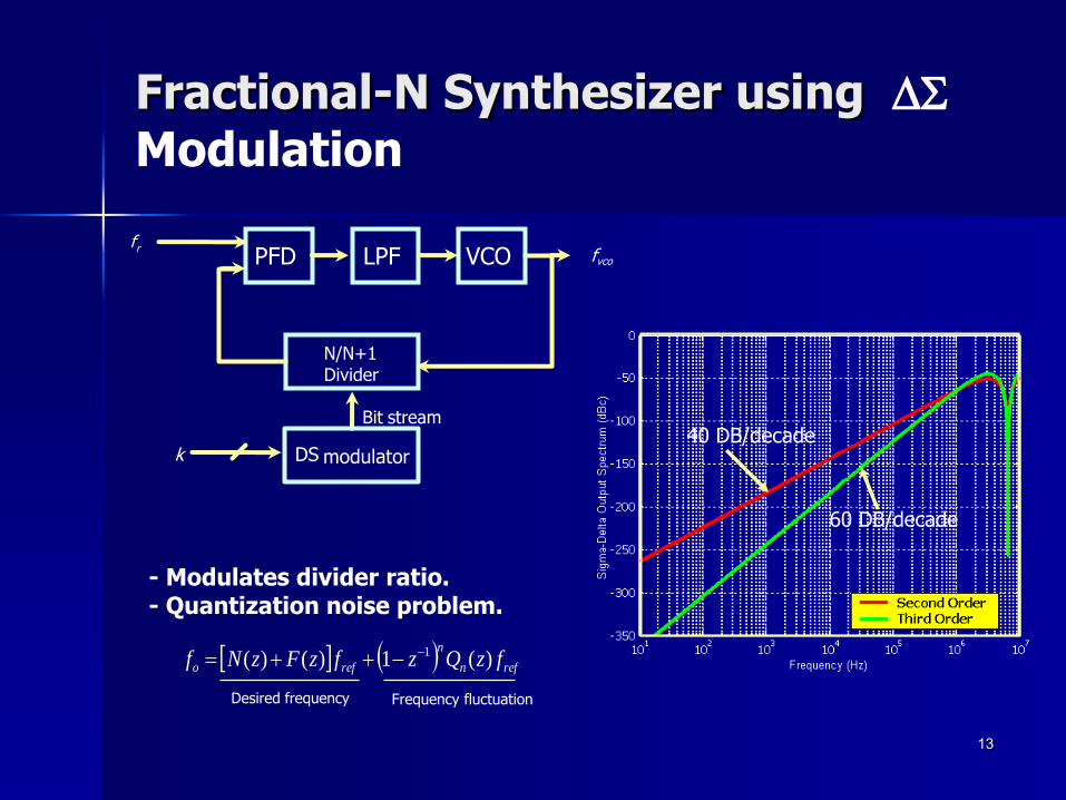
Fractional-N Synthesizer using DSModulation
refn
n
refo fzQzfzFzNf )(1)()( 1++=
Desired frequency Frequency fluctuation
- Modulates divider ratio.- Quantization noise problem.
PFD
N/N+1Divider
rf
k
streamBit
vcofLPF VCO
modulatorDS40 DB/decade
60 DB/decade
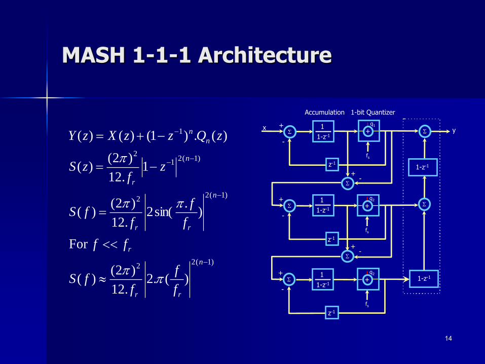
14
MASH 1-1-1 Architecture
)(.2.12
)2()(
For
).
sin(2.12
)2()(
1.12
)2()(
)(.)1()()(
)1(22
)1(22
)1(21
2
1
=
=
+=
n
rr
r
n
rr
n
r
n
n
f
f
ffS
ff
f
f
ffS
zf
zS
zQzzXzY
Accumulation 1-bit Quantizer
x +
-
S
+
-
S
+
-
S
+-
S
+-
S
1
1-z-1
1
1-z-1
1
1-z-1
+q1
fs
+q2
fs
+q2
fs
S
S
y
1-z-1
1-z-1
z-1
z-1
z-1
15
Outline
Motivation
Background
Novel Fractional-N Frequency Synthesizers
Novel Analog-to-Digital Architecture
Conclusions
16
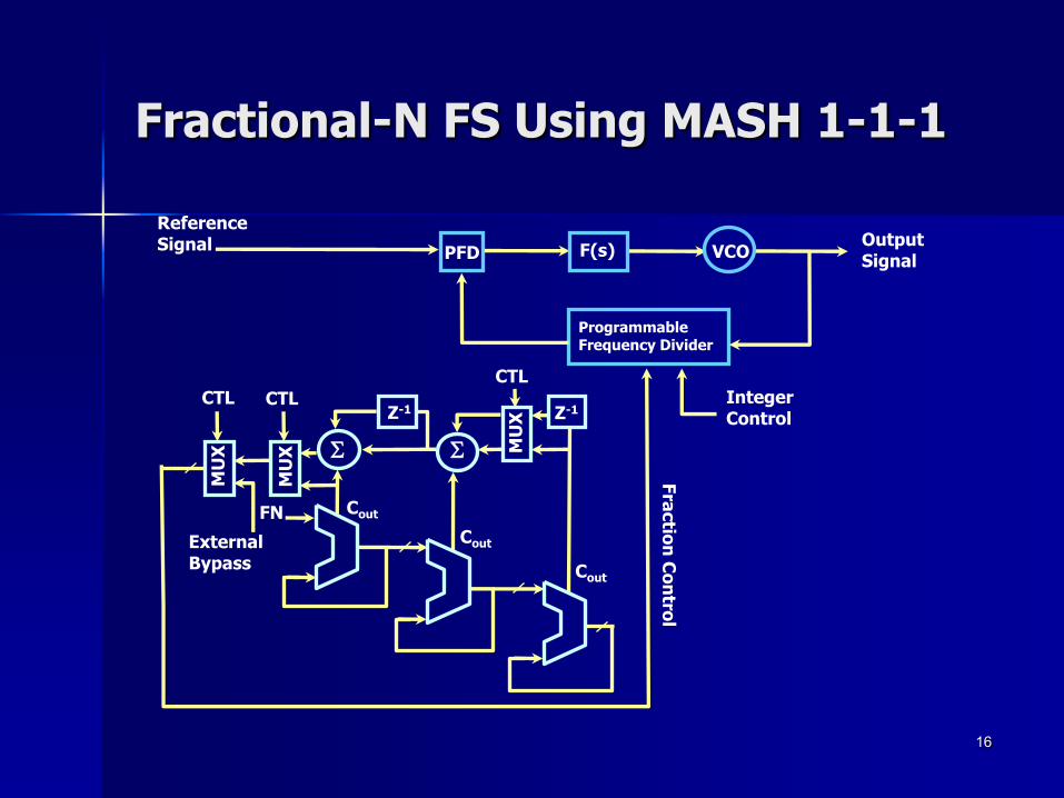
Fractional-N FS Using MASH 1-1-1
S S
CTL CTL
CTL
MU
X
MU
X MU
XZ-1 Z-1
ExternalBypass
FN Cout
Cout
Cout
ReferenceSignal PFD F(s) VCO
Programmable Frequency Divider
IntegerControl
Fra
ctio
n C
on
trol
OutputSignal
17
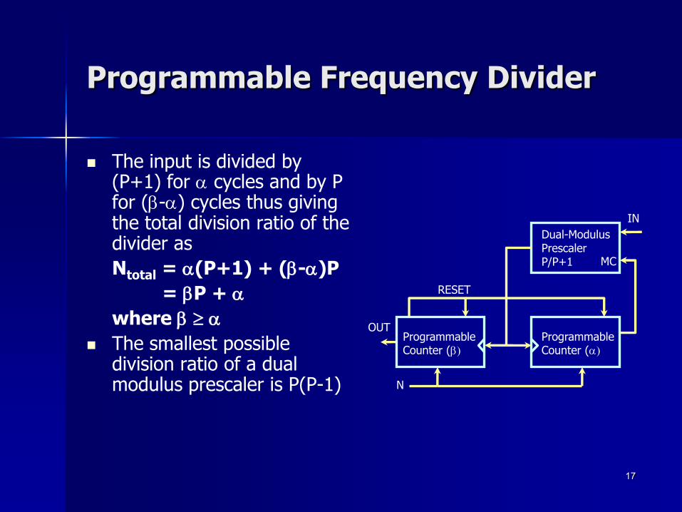
The input is divided by (P+1) for a cycles and by P for (b-a) cycles thus giving the total division ratio of the divider as
Ntotal = a(P+1) + (b-a)P
= bP + a
where b a
The smallest possible division ratio of a dual modulus prescaler is P(P-1)
Programmable Frequency Divider
IN
Dual-ModulusPrescalerP/P+1 MC
RESET
OUT
N
ProgrammableCounter (b
ProgrammableCounter (a
18
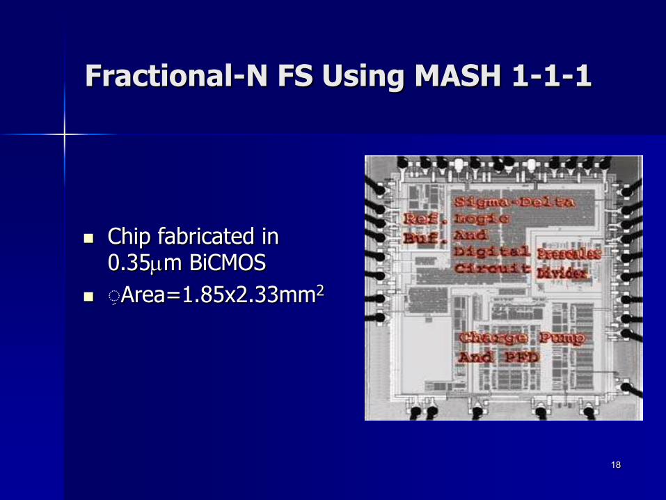
Fractional-N FS Using MASH 1-1-1
Chip fabricated in 0.35mm BiCMOS
Area=1.85x2.33mm2
19
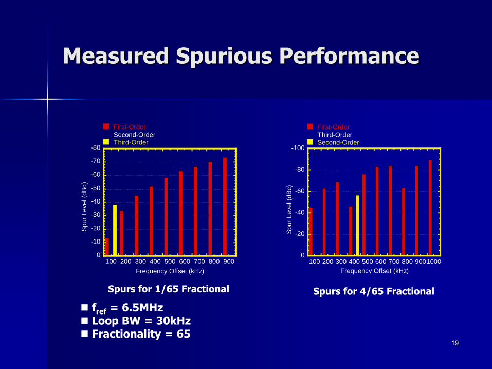
Measured Spurious Performance
Spurs for 1/65 Fractional Spurs for 4/65 Fractional
-100
-80
-60
-40
-20
0100 200 300 400 500 600 700 800 9001000
First-OrderThird-OrderSecond-Order
Sp
ur
Leve
l (d
Bc)
Frequency Offset (kHz)
-80
-70
-60
-50
-40
-30
-20
-10
0100 200 300 400 500 600 700 800 900
First-OrderSecond-OrderThird-Order
Sp
ur
Leve
l (d
Bc)
Frequency Offset (kHz)
fref = 6.5MHz Loop BW = 30kHz Fractionality = 65
20
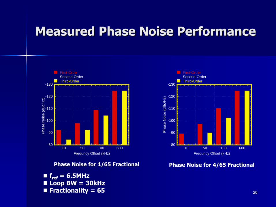
Measured Phase Noise Performance
Phase Noise for 1/65 Fractional Phase Noise for 4/65 Fractional
-130
-120
-110
-100
-90
-8010 50 100 600
First-OrderSecond-OrderThird-Order
Ph
ase
No
ise (
dB
c/H
z)
Frequncy Offset (kHz)
-130
-120
-110
-100
-90
-8010 50 100 600
First-OrderSecond-OrderThird-Order
Ph
ase
No
ise (
dB
c/H
z)
Frequncy Offset (kHz)
fref = 6.5MHz Loop BW = 30kHz Fractionality = 65
21
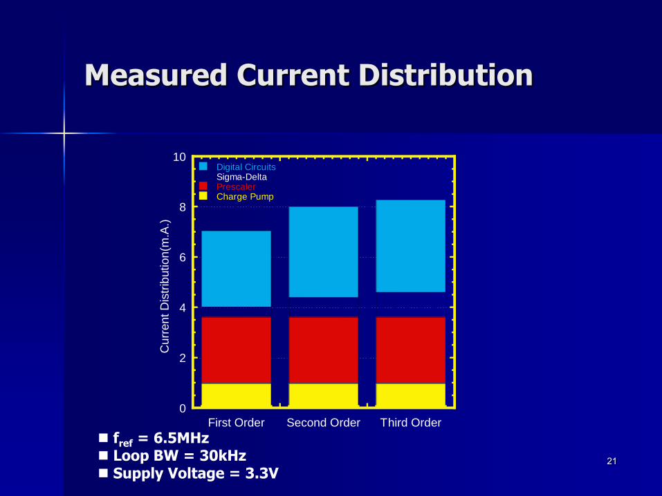
Measured Current Distribution
0
2
4
6
8
10
First Order Second Order Third Order
Digital CircuitsSigma-DeltaPrescalerCharge Pump
Curr
ent D
istr
ibution(m
.A.)
fref = 6.5MHz Loop BW = 30kHz Supply Voltage = 3.3V
22
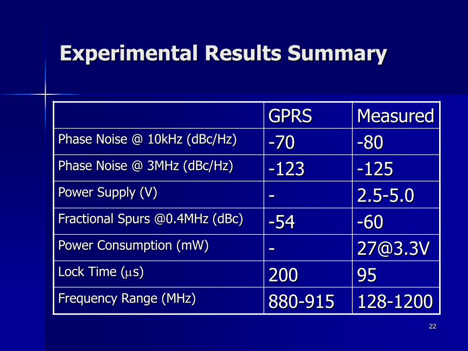
Experimental Results Summary
GPRS MeasuredPhase Noise @ 10kHz (dBc/Hz) -70 -80Phase Noise @ 3MHz (dBc/Hz) -123 -125Power Supply (V) - 2.5-5.0Fractional Spurs @0.4MHz (dBc) -54 -60Power Consumption (mW) - [email protected] Time (ms) 200 95Frequency Range (MHz) 880-915 128-1200
23
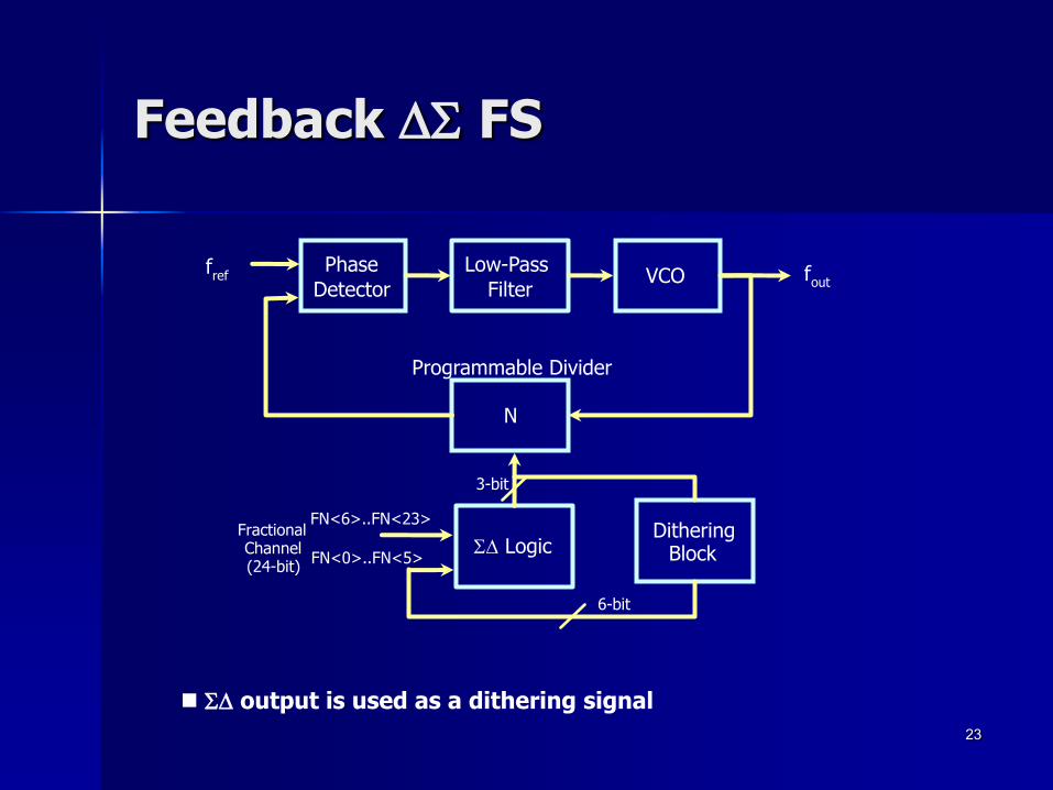
Feedback DS FS
Phase
Detector
Low-Pass
FilterVCO
N
fref
FractionalChannel(24-bit)
Programmable Divider
SD Logic
fout
3-bit
FN<0>..FN<5>
FN<6>..FN<23>Dithering
Block
6-bit
SD output is used as a dithering signal
24
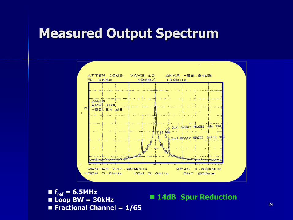
Measured Output Spectrum
14dB Spur Reduction fref = 6.5MHz Loop BW = 30kHz Fractional Channel = 1/65
25
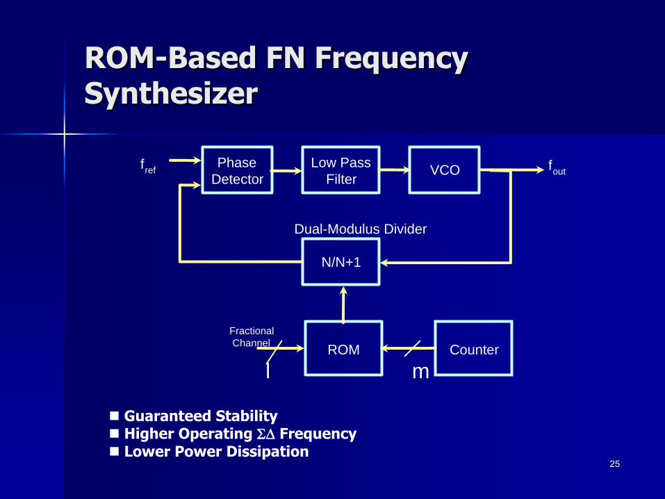
ROM-Based FN Frequency Synthesizer
Phase
Detector
Low Pass
FilterVCO
N/N+1
fref
Fractional
Channel
Dual-Modulus Divider
ROM Counter
l m
fout
Guaranteed Stability Higher Operating SD Frequency Lower Power Dissipation
26
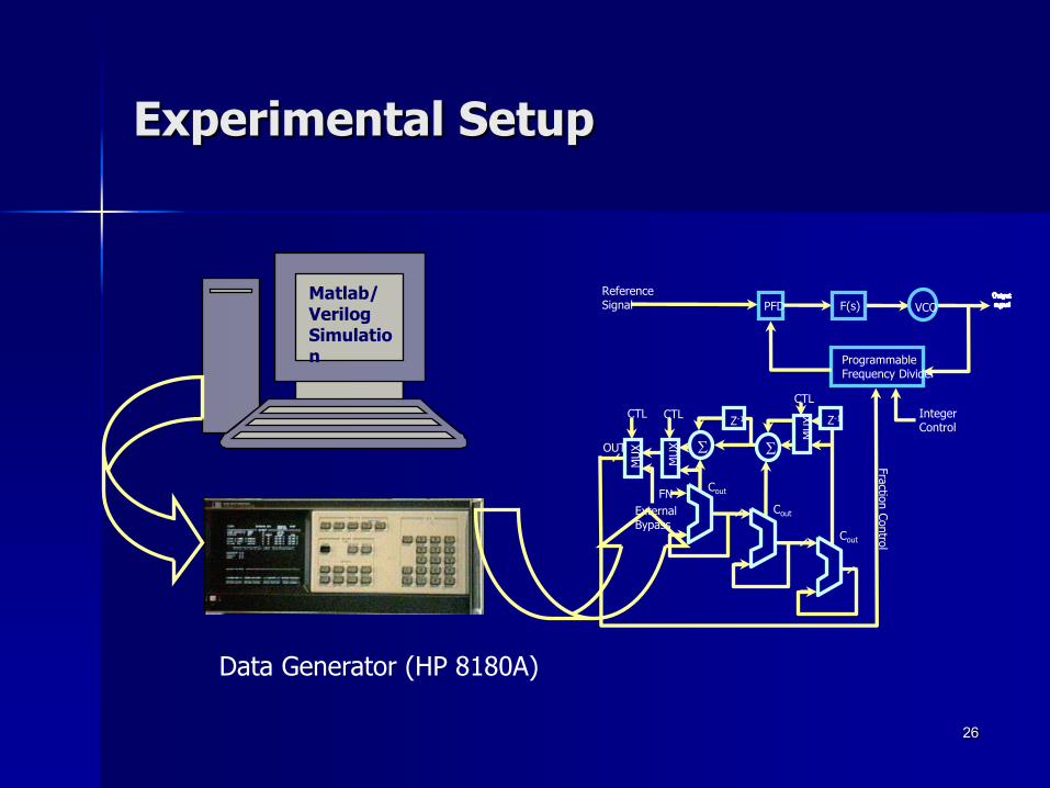
Experimental Setup
Matlab/ VerilogSimulation
S S
CTL CTL
CTL
OUT
MU
X
MU
X
MU
XZ-1 Z-1
ExternalBypass
FNCout
Cout
Cout
ReferenceSignal PFD F(s) VCO
Programmable Frequency Divider
IntegerControl
Fra
ction C
ontro
l
Data Generator (HP 8180A)
27
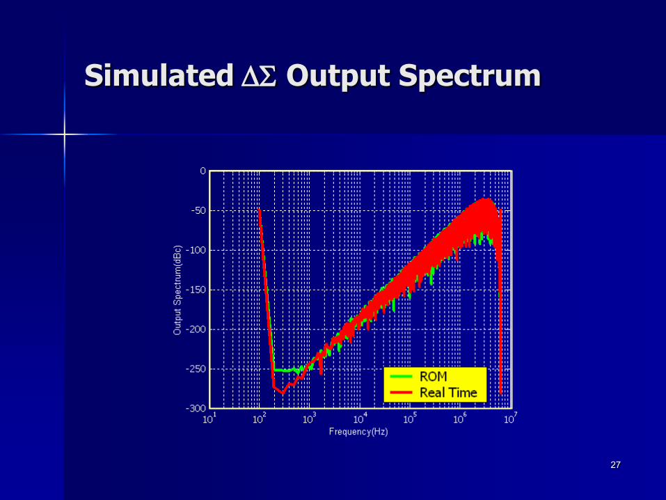
Simulated DS Output Spectrum
28
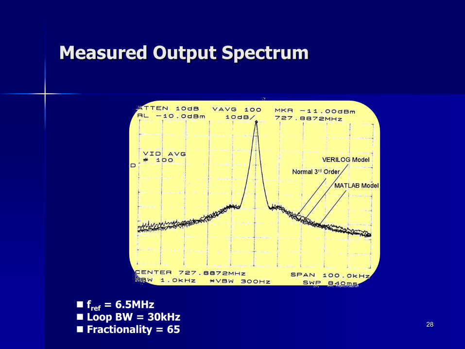
Measured Output Spectrum
fref = 6.5MHz Loop BW = 30kHz Fractionality = 65
29
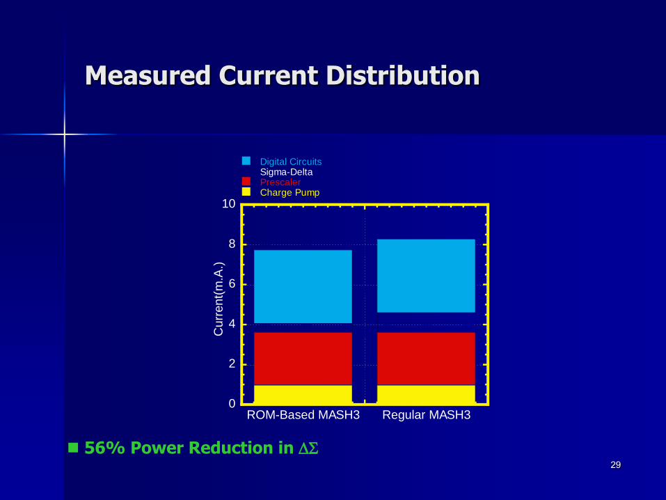
Measured Current Distribution
56% Power Reduction in DS
0
2
4
6
8
10
ROM-Based MASH3 Regular MASH3
Digital CircuitsSigma-DeltaPrescalerCharge Pump
Cu
rren
t(m
.A.)
30
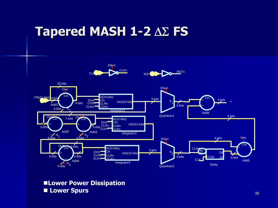
Tapered MASH 1-2 DS FS
Cin+
-
Cin+
+Add1
Add4
Add2 Add3
Add6
Add5
Delay
Quantizer1
Quantizer2
CLKCLKn
DSon
RSTRSTn
CLKp
ApBp Qp
Qn
Cin
+
-
CLRnCLKn
A(24-bits)Cin
Int1(24-bits)ZeroCLRn
CLKn
Integrator1
CLRnCLKn
A(10-bits)Cin
Int3(10-bits)ZeroCLRnCLKn
Integrator3
ZeroCLRnCLKn
A(12-bits)Cin
CLRnCLKn
Int2(12-bits)
Integrator2
Cin
+
-
Cin
+
-
Cin
+
-
DSon
DSon
FN(21-bits)
CLRn
CLK
One
One
One One
One
Y
20-bits
4-bits
4-bits
4-bits
5-bits
5-bits
5-bits
7-bits
5-bits
5-bits
5-bits
5-bits
5-bits
5-bits
5-bits
3-bits
3-bits 3-bits
3-bits
3-bits
4-bitsq1
q2
q1
q1
q2
q2
Lower Power Dissipation Lower Spurs
31
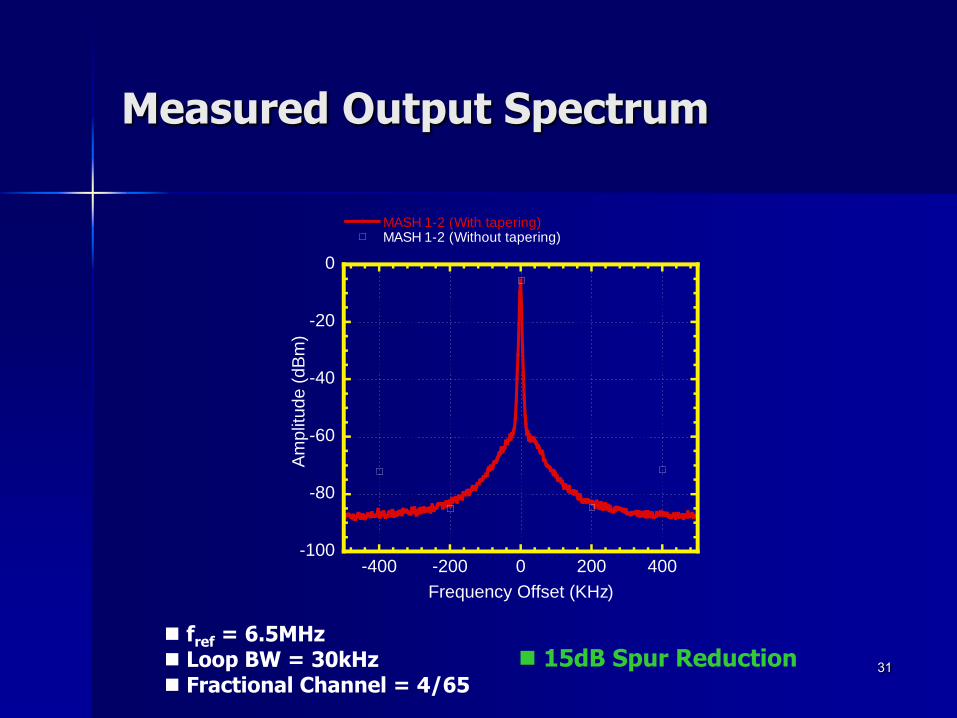
Measured Output Spectrum
15dB Spur Reduction
-100
-80
-60
-40
-20
0
-400 -200 0 200 400
MASH 1-2 (With tapering)MASH 1-2 (Without tapering)
Am
plit
ud
e (
dB
m)
Frequency Offset (KHz)
fref = 6.5MHz Loop BW = 30kHz Fractional Channel = 4/65
32
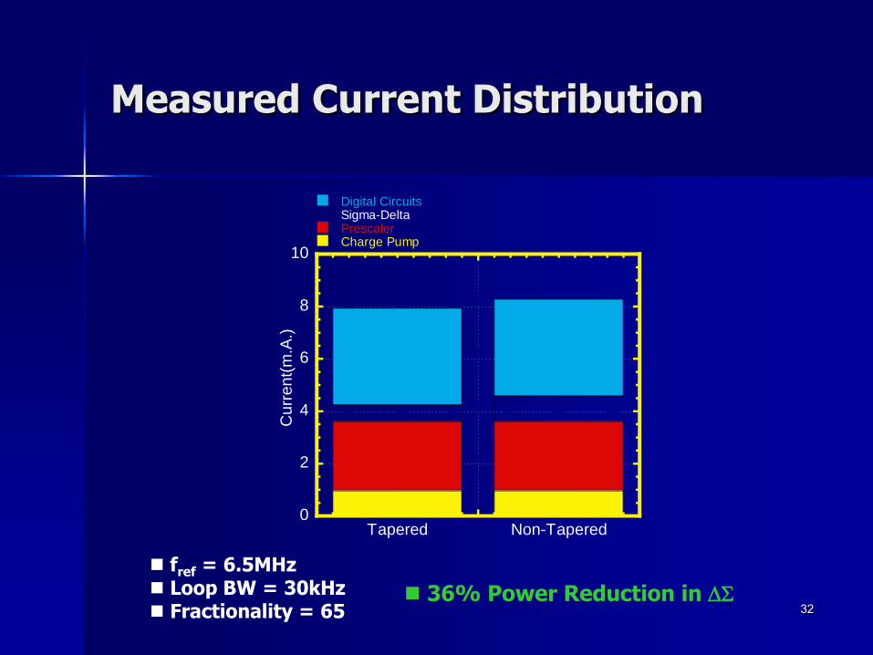
Measured Current Distribution
36% Power Reduction in DS
0
2
4
6
8
10
Tapered Non-Tapered
Digital CircuitsSigma-DeltaPrescalerCharge Pump
Cu
rren
t(m
.A.)
fref = 6.5MHz Loop BW = 30kHz Fractionality = 65
33
Outline
Motivation
Background
Novel Fractional-N Frequency Synthesizers
Novel Analog-to-Digital Architecture
Conclusions
34
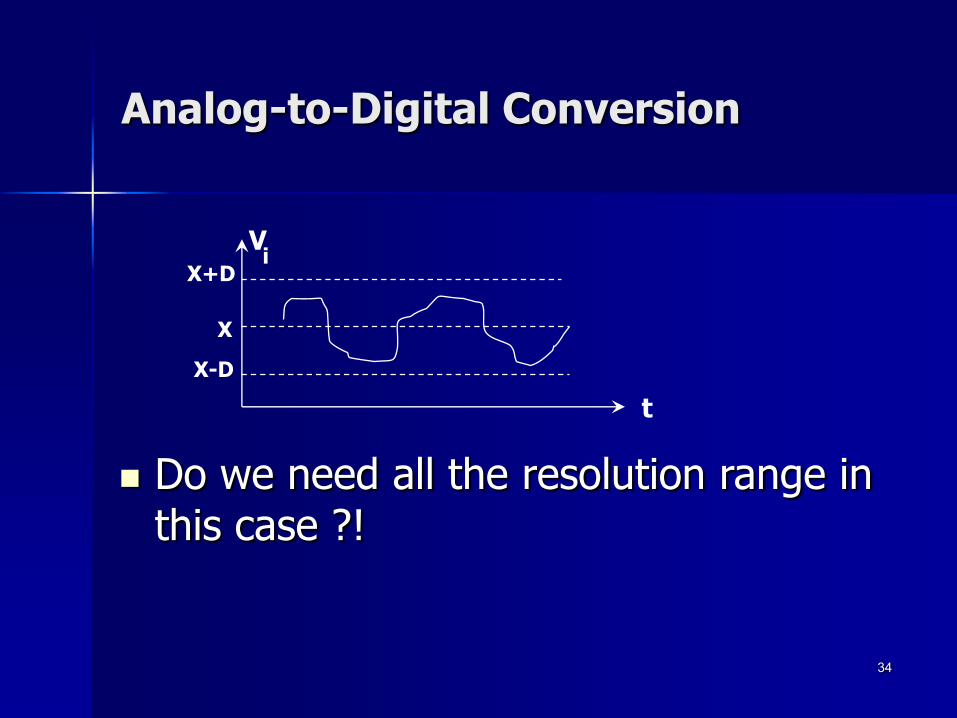
Analog-to-Digital Conversion
Do we need all the resolution range in this case ?!
X
X+D
X-D
t
Vi
35
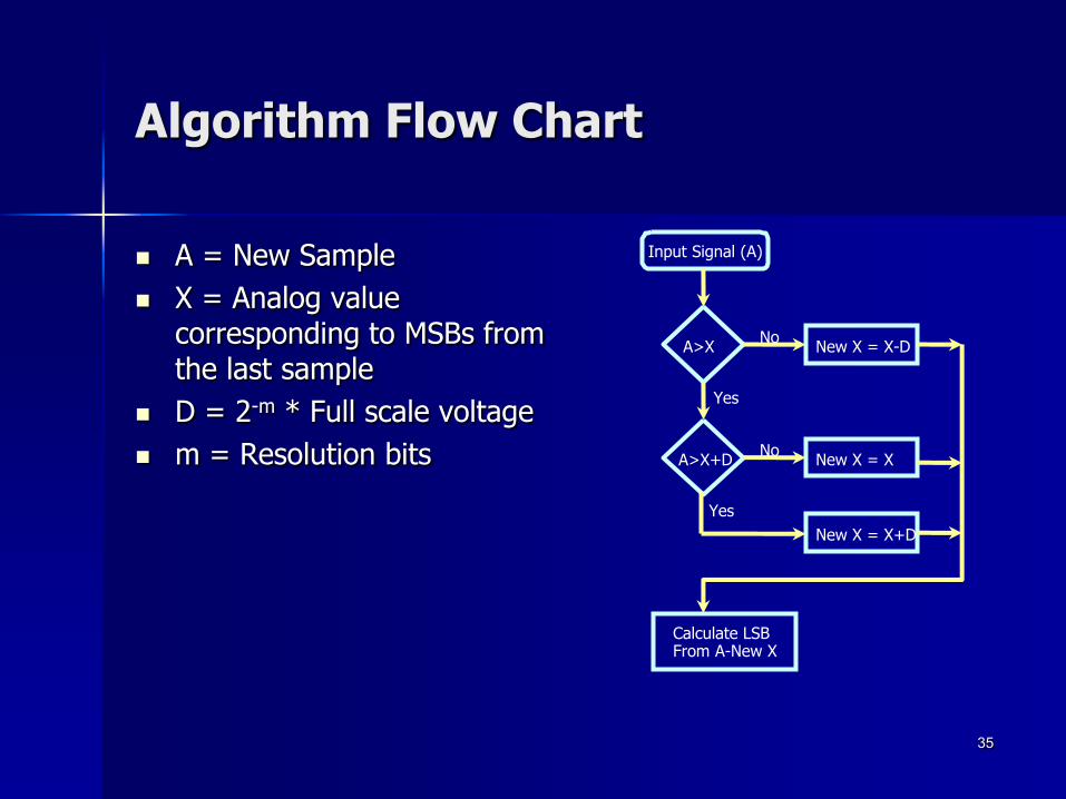
Algorithm Flow Chart
A = New Sample
X = Analog value corresponding to MSBs from the last sample
D = 2-m * Full scale voltage
m = Resolution bits
Calculate LSBFrom A-New X
Input Signal (A)
A>X
Yes
No
No
Yes
New X = X-D
A>X+D
New X = X+D
New X = X
36
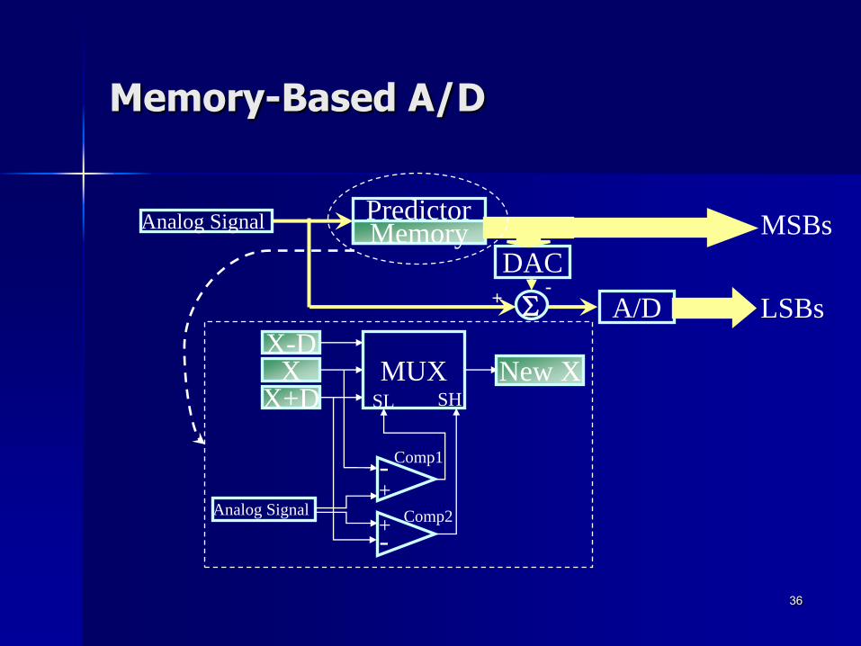
Memory-Based A/D
MUXX-D
XX+D
New X
Analog Signal
-
-
+
+
Comp1
Comp2
SL SH
A/D
Analog SignalMemoryPredictor
MSBs
LSBs
DAC
S+-
37
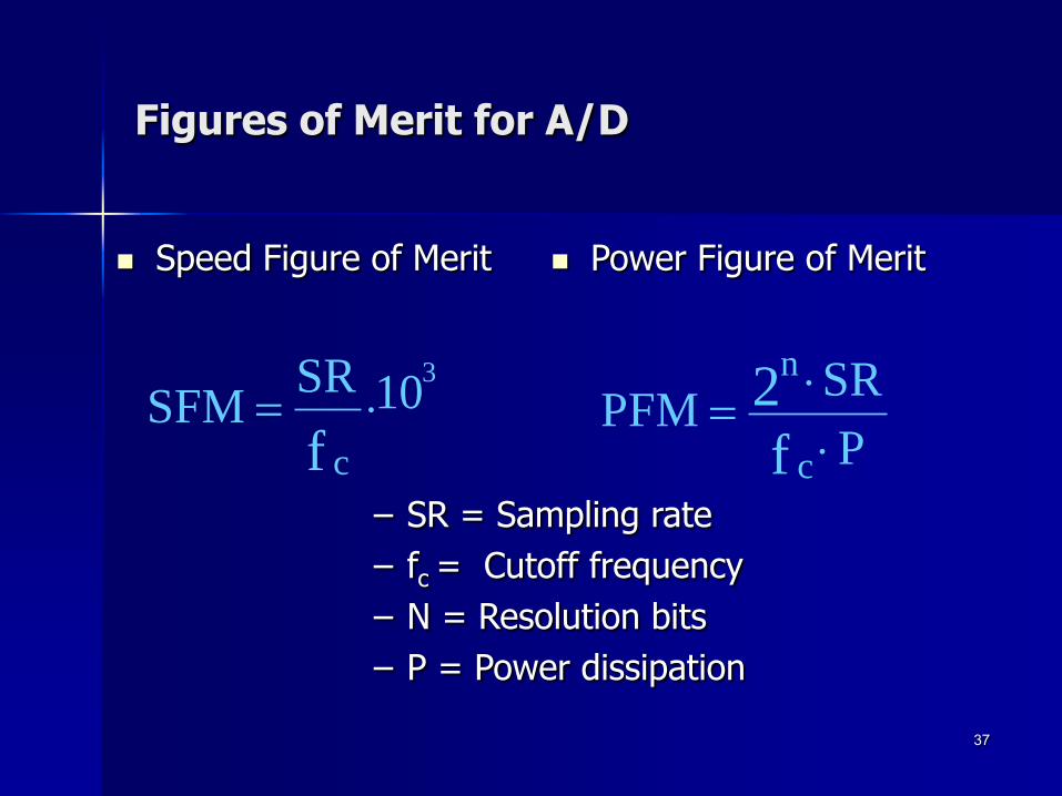
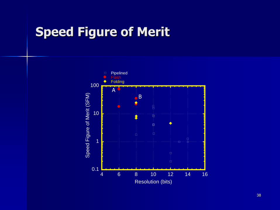
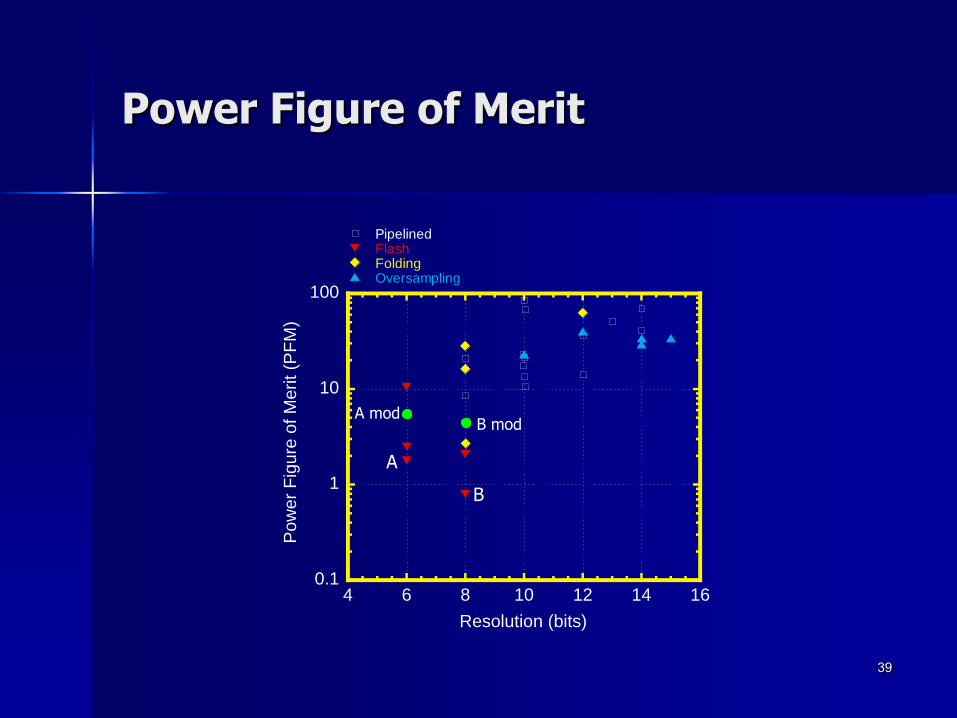
Figures of Merit for A/D
Speed Figure of Merit
10SRSFM
3
f c
=
Power Figure of Merit
P
SRPFM
f
2
c
n
=
– SR = Sampling rate
– fc = Cutoff frequency
– N = Resolution bits
– P = Power dissipation
38
Speed Figure of Merit
A
B
0.1
1
10
100
4 6 8 10 12 14 16
PipelinedFlashFolding
Speed F
igure
of M
erit (S
FM
)
Resolution (bits)
39
Power Figure of Merit
0.1
1
10
100
4 6 8 10 12 14 16
PipelinedFlashFoldingOversampling
Pow
er
Fig
ure
of M
erit (P
FM
)
Resolution (bits)
A
B
A modB mod
40
Outline
Motivation
Background
Novel Fractional-N Frequency Synthesizers
Novel Analog-to-Digital Architecture
Conclusions
41
Conclusions
Enhancing the lock time, phase noise, and reference spurs are possible with fractional-N frequency synthesizers
A 1.2 GHz fractional-N frequency synthesizer is presented with MASH architecture and pulse-swallowed dual-modulus divider, in 0.35mm BiCOMS
Measured performance meets the GPRS requirements– Lock Time =95ms, in-band phase noise= -80 dBc/Hz, and
out-of-band phase noise= -125 dBc/Hz at 3MHz
DS output may be used as a dithering signal to reduce the spurs
42
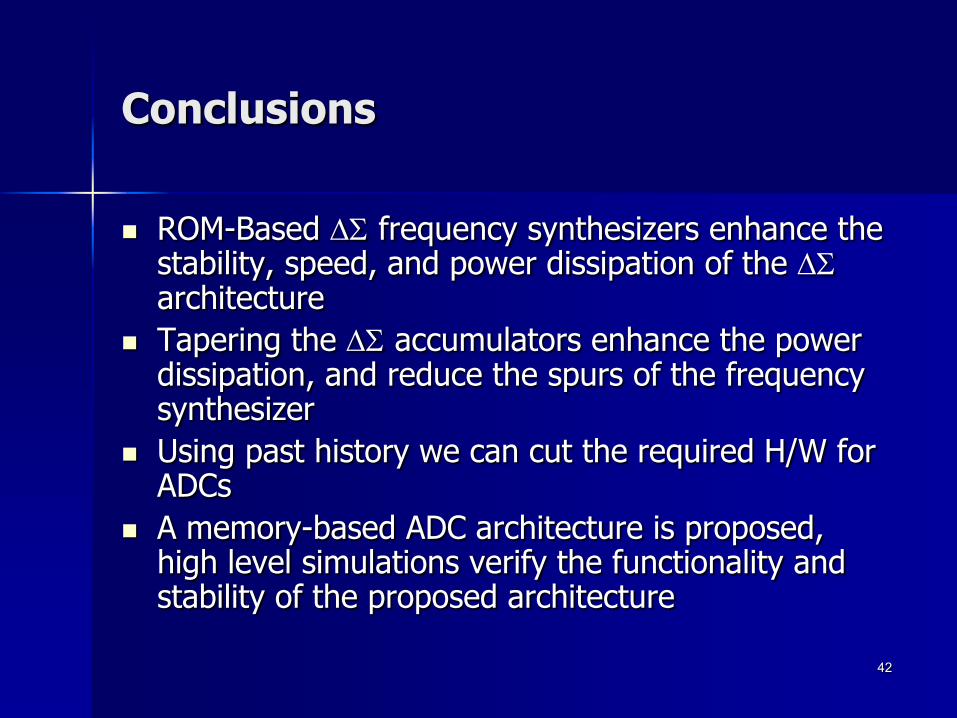
Conclusions
ROM-Based DS frequency synthesizers enhance the stability, speed, and power dissipation of the DSarchitecture
Tapering the DS accumulators enhance the power dissipation, and reduce the spurs of the frequency synthesizer
Using past history we can cut the required H/W for ADCs
A memory-based ADC architecture is proposed, high level simulations verify the functionality and stability of the proposed architecture
43
Future Work
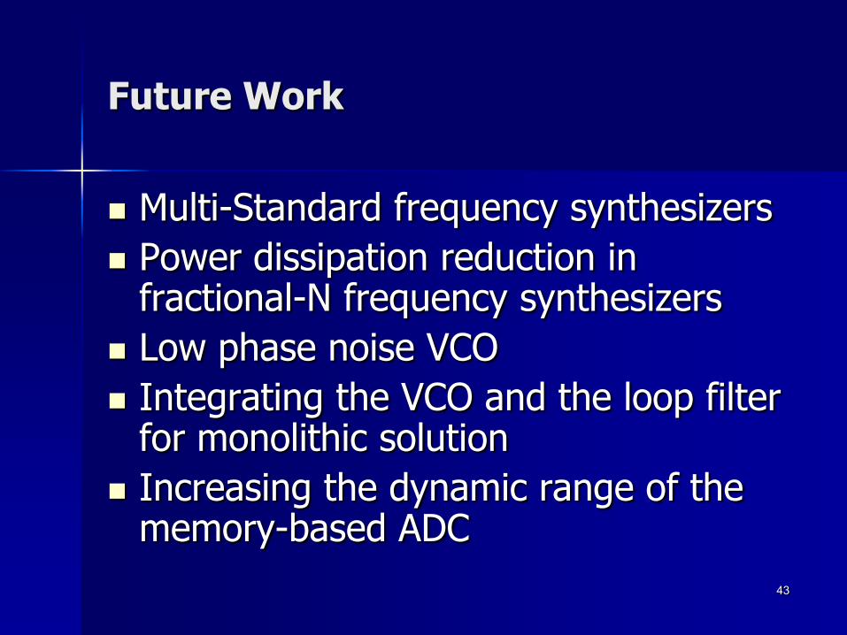
Multi-Standard frequency synthesizers
Power dissipation reduction in fractional-N frequency synthesizers
Low phase noise VCO
Integrating the VCO and the loop filter for monolithic solution
Increasing the dynamic range of the memory-based ADC
44
Publications
A. E. Hussein and M. I. Elmasry, "A ROM Based Fractional-N Frequency Synthesizer for Wireless Communication," in Proc. of Midwest Symposium on VLSI, August 2002, Tulsa, U.S.A.
A. E. Hussein and M. I. Elmasry,"A Fractional-N Frequency Synthesizer for Wireless Communications," in Proc. of IEEE International Symposium on Circuits and Systems, vol.4, pp.513-516, May 2002, Arizona, U.S.A.
A. E. Hussein and M. I. Elmasry, "Low Power Analog-to-Digital Converter for Wireless Communication," in Proc. of 10th ACM Great Lakes Symposium on VLSI, March 2000, Chicago, U.S.A.
A. E. Hussein, M. A. Hasan, and M. I. Elmasry, "A New Algorithm for the Division in the Residue Number System (RNS) For Low Power Applications," in Proc. of CCECE’98, vol.1, pp.205-208, May 1998, Waterloo, ON, Canada.
A. E. Hussein and M. I. Elmasry,"A Novel Fractional-N Frequency Synthesizers for Wireless Communications," IEEE Journal of Solid-State Circuits (in preparation)
A. E. Hussein and M. I. Elmasry, “A Low Power Analog-to-Digital Converter for Wireless Communication," IEEE Transactions on Circuits and Systems II (in preparation)