Embed Size (px)
Citation preview
676doi:10.1017/S1431927618003872
Microsc. Microanal. 24 (Suppl 1), 2018© Microscopy Society of America 2018
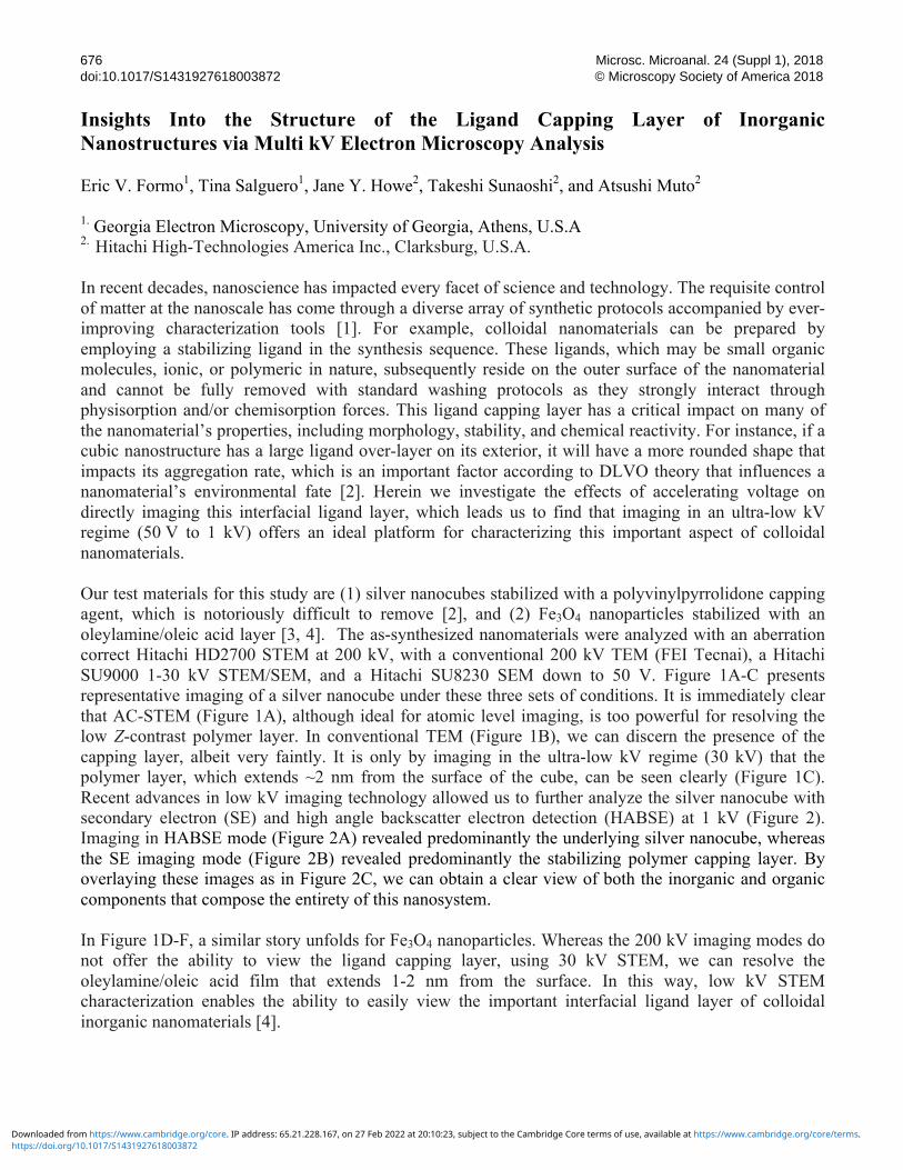
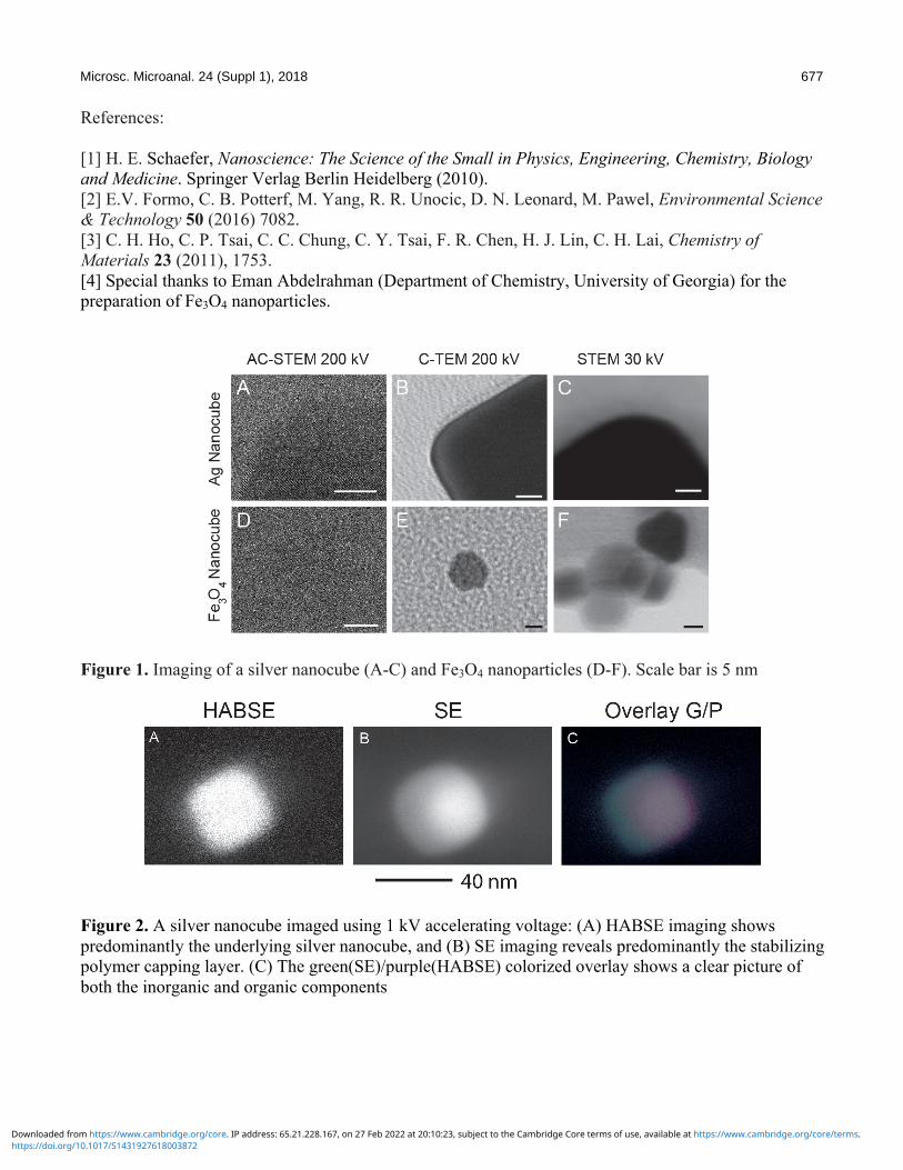
Insights Into the Structure of the Ligand Capping Layer of Inorganic Nanostructures via Multi kV Electron Microscopy Analysis Eric V. Formo1, Tina Salguero1, Jane Y. Howe2, Takeshi Sunaoshi2, and Atsushi Muto2 1. Georgia Electron Microscopy, University of Georgia, Athens, U.S.A 2. Hitachi High-Technologies America Inc., Clarksburg, U.S.A. In recent decades, nanoscience has impacted every facet of science and technology. The requisite control of matter at the nanoscale has come through a diverse array of synthetic protocols accompanied by ever-improving characterization tools [1]. For example, colloidal nanomaterials can be prepared by employing a stabilizing ligand in the synthesis sequence. These ligands, which may be small organic molecules, ionic, or polymeric in nature, subsequently reside on the outer surface of the nanomaterial and cannot be fully removed with standard washing protocols as they strongly interact through physisorption and/or chemisorption forces. This ligand capping layer has a critical impact on many of the nanomaterial’s properties, including morphology, stability, and chemical reactivity. For instance, if a cubic nanostructure has a large ligand over-layer on its exterior, it will have a more rounded shape that impacts its aggregation rate, which is an important factor according to DLVO theory that influences a nanomaterial’s environmental fate [2]. Herein we investigate the effects of accelerating voltage on directly imaging this interfacial ligand layer, which leads us to find that imaging in an ultra-low kV regime (50 V to 1 kV) offers an ideal platform for characterizing this important aspect of colloidal nanomaterials. Our test materials for this study are (1) silver nanocubes stabilized with a polyvinylpyrrolidone capping agent, which is notoriously difficult to remove [2], and (2) Fe3O4 nanoparticles stabilized with an oleylamine/oleic acid layer [3, 4]. The as-synthesized nanomaterials were analyzed with an aberration correct Hitachi HD2700 STEM at 200 kV, with a conventional 200 kV TEM (FEI Tecnai), a Hitachi SU9000 1-30 kV STEM/SEM, and a Hitachi SU8230 SEM down to 50 V. Figure 1A-C presents representative imaging of a silver nanocube under these three sets of conditions. It is immediately clear that AC-STEM (Figure 1A), although ideal for atomic level imaging, is too powerful for resolving the low Z-contrast polymer layer. In conventional TEM (Figure 1B), we can discern the presence of the capping layer, albeit very faintly. It is only by imaging in the ultra-low kV regime (30 kV) that the polymer layer, which extends ~2 nm from the surface of the cube, can be seen clearly (Figure 1C). Recent advances in low kV imaging technology allowed us to further analyze the silver nanocube with secondary electron (SE) and high angle backscatter electron detection (HABSE) at 1 kV (Figure 2). Imaging in HABSE mode (Figure 2A) revealed predominantly the underlying silver nanocube, whereas the SE imaging mode (Figure 2B) revealed predominantly the stabilizing polymer capping layer. By overlaying these images as in Figure 2C, we can obtain a clear view of both the inorganic and organic components that compose the entirety of this nanosystem. In Figure 1D-F, a similar story unfolds for Fe3O4 nanoparticles. Whereas the 200 kV imaging modes do not offer the ability to view the ligand capping layer, using 30 kV STEM, we can resolve the oleylamine/oleic acid film that extends 1-2 nm from the surface. In this way, low kV STEM characterization enables the ability to easily view the important interfacial ligand layer of colloidal inorganic nanomaterials [4].
https://doi.org/10.1017/S1431927618003872Downloaded from https://www.cambridge.org/core. IP address: 65.21.228.167, on 27 Feb 2022 at 20:10:23, subject to the Cambridge Core terms of use, available at https://www.cambridge.org/core/terms.
Microsc. Microanal. 24 (Suppl 1), 2018 677
References: [1] H. E. Schaefer, Nanoscience: The Science of the Small in Physics, Engineering, Chemistry, Biology and Medicine. Springer Verlag Berlin Heidelberg (2010). [2] E.V. Formo, C. B. Potterf, M. Yang, R. R. Unocic, D. N. Leonard, M. Pawel, Environmental Science & Technology 50 (2016) 7082. [3] C. H. Ho, C. P. Tsai, C. C. Chung, C. Y. Tsai, F. R. Chen, H. J. Lin, C. H. Lai, Chemistry of Materials 23 (2011), 1753. [4] Special thanks to Eman Abdelrahman (Department of Chemistry, University of Georgia) for the preparation of Fe3O4 nanoparticles.
Figure 1. Imaging of a silver nanocube (A-C) and Fe3O4 nanoparticles (D-F). Scale bar is 5 nm
Figure 2. A silver nanocube imaged using 1 kV accelerating voltage: (A) HABSE imaging shows predominantly the underlying silver nanocube, and (B) SE imaging reveals predominantly the stabilizing polymer capping layer. (C) The green(SE)/purple(HABSE) colorized overlay shows a clear picture of both the inorganic and organic components
https://doi.org/10.1017/S1431927618003872Downloaded from https://www.cambridge.org/core. IP address: 65.21.228.167, on 27 Feb 2022 at 20:10:23, subject to the Cambridge Core terms of use, available at https://www.cambridge.org/core/terms.