Embed Size (px)
Citation preview

Självständigt arbete på avancerad nivå
Independent degree project second cycle
Electronics, 30 credits
Design and Implementation of a High Frequency Flyback Converter
Nisar Ahmad

Design and Implementation of a
High Frequency Flyback
Converter
Nisar Ahmad
2015-03-17
ii
Mid Sweden University Department of Electronics Design Author: Nisar Ahmad, [email protected], [email protected] Study Programme: International Master’s Programme in Electronics Design, 120 credits Supervisor: Kent Bertilsson, [email protected] Examiner: Bengt Oelmann, [email protected] Date: 2014-04-15
Design and Implementation of a
High Frequency Flyback
Converter
Nisar Ahmad
Abstract
2015-03-17
iii
Abstract The power supply designers choose flyback topology due to its promis-
ing features of design simplicity, cost effectiveness and multiple outputs
handling capability. The designed product based on flyback topology
should be smaller in size, cost effective and energy efficient. Similarly,
designers focus on reducing the circuit losses while operating at high
frequencies that affect the converter efficiency and performance. Based
on the above circumstances, an energy efficient open loop high frequen-
cy flyback converter is designed and operated in MHz frequency region
using step down multilayer PCB planar transformer. The maximum
efficiency of 84.75% is observed and maximum output power level
reached is 22.8W. To overcome the switching losses, quasi-resonant soft
switching technique is adopted and a high voltage CoolMOS power
transistor is used.
Keywords: Flyback Converter, Quasi-Resonant Soft Switching Tech-
nique.

Design and Implementation of a
High Frequency Flyback
Converter
Nisar Ahmad
Acknowledgements/Foreword
2015-03-17
iv
Acknowledgements/Foreword I am grateful to my supervisor Dr. Kent Bertilsson for showing great
interest, kind collaboration and valuable guidance. His positive and
encouraging attitude throughout thesis work is highly appreciated.
I express my sincere thanks to my parents, family members and friends
for their support and best wishes.
Design and Implementation of a
High Frequency Flyback
Converter
Nisar Ahmad
Table of Contents
2015-03-17
v
Table of Contents
Abstract ............................................................................................................ iii
Acknowledgements/Foreword .................................................................... iv
Table of Contents ............................................................................................. v
List of Figures ................................................................................................... 1
List of Tables ..................................................................................................... 1
1 Introduction ............................................................................................ 1
1.1 Background and problem motivation ...................................... 1
1.2 Overall aim ................................................................................... 2
1.3 Clear and Verifiable Goals ......................................................... 2
1.4 Scope ............................................................................................. 2
1.5 Outline .......................................................................................... 3
2 Theory ...................................................................................................... 4
2.1 Linear Power Supply .................................................................. 4
2.2 Switched Mode Power Supply .................................................. 5
2.3 DC-DC Power Converter ........................................................... 6
2.3.1 Boost Converter ................................................................ 6
2.3.2 Buck Converter ................................................................. 8
2.3.3 Flyback Converter ............................................................ 9
2.4 Conduction Modes .................................................................... 15
2.4.1 Continuous Conduction Mode (CCM) ........................ 15
2.4.2 Discontinuous Conduction Mode (DCM) ................... 16
2.5 Switching Techniques ............................................................... 18
2.5.1 Hard Switching ............................................................... 18
2.5.1.1 Hard Switching Issues ................................................... 18
2.5.2 Soft Switching ................................................................. 19
2.5.2.1 Zero Current Switching ................................................. 20
2.5.2.2 Zero Voltage Switching ................................................. 20
3 Related Work ........................................................................................ 21
4 Methodology/Model ........................................................................... 26
4.1 Converter Circuit Design ......................................................... 26
4.2 PCB Design for Converter ........................................................ 26
Design and Implementation of a
High Frequency Flyback
Converter
Nisar Ahmad
Table of Contents
2015-03-17
vi
4.3 Switch Control using dsPIC Processor ................................... 26
4.4 Converter Integration by Utilizing Planar Transformer ..... 27
5 Design and Implementation ............................................................. 28
5.1 Converter Main Modules ......................................................... 28
5.2 Converter Hardware Design ................................................... 29
5.2.1 dsPIC33FJ16GS502 Microcontroller ............................. 29
5.2.2 Gate Driver ...................................................................... 29
5.2.3 CoolMOS IPL60R385CP Power MOSFET ................... 30
5.2.4 Transformer and Load ................................................... 31
5.2.5 Circuit and PCB Design for Converter ........................ 31
5.3 Converter Implementation ...................................................... 37
5.3.1 Gate Driver Signal .......................................................... 38
5.3.2 Converter Open Loop control ...................................... 39
6 Results ................................................................................................... 42
6.1 Quasi Resonant Mode ............................................................... 42
6.1.1 Parameters Variance ...................................................... 42
6.1.1.1 Input Voltage .................................................................. 42
6.1.1.2 Duty Cycle ....................................................................... 46
6.1.1.3 Connected Load .............................................................. 49
7 Discussion ............................................................................................. 50
7.1 Ethics and Impact on Society ................................................... 51
8 Conclusion ............................................................................................ 52
8.1 Future Work ............................................................................... 52
References ........................................................................................................ 53

Design and Implementation of a
High Frequency Flyback
Converter
Nisar Ahmad
List of Figures
2015-03-17
1
List of Figures
Figure 1: Block diagram of linear power supply ................................................................... 4 Figure 2: Block diagram of switched-mode power supply [3] ............................................ 5 Figure 3: Boost converter basic schematic with parasitics [4] ............................................. 7 Figure 4: A buck converter basic schematic [5] ...................................................................... 8 Figure 5: Flyback converter [8]................................................................................................. 9 Figure 6: Converter operation in the switch ON state [7] .................................................. 10 Figure 7: Equivalent circuit in the switch ON state [7] ....................................................... 11 Figure 8: Converter operation in the switch OFF state [7] ................................................. 12 Figure 9: Flyback converter waveforms [9] .......................................................................... 13 Figure 10: Equivalent circuit in switch OFF state ................................................................ 14 Figure 11: Continuous Conduction Mode operation [10] .................................................. 15 Figure 12: Discontinuous Conduction Mode operation [10] ............................................. 17 Figure 13: Hard switching and its losses [12] ...................................................................... 19 Figure 14: (a) Cross-sectional view and 3D view of coreless PCB transformer. (b) Three
dimensional view of multilayer coreless PCB power transformer PSSP structure
[18] .................................................................................................................................... 23 Figure 15: POT core design [19] ............................................................................................. 24 Figure 16: Multilayer PCB Transformer (centre) with POT core....................................... 25 Figure 17: System block diagram ........................................................................................... 28 Figure 18: dsPIC33FJ16GS502 pin diagram [20] .................................................................. 29 Figure 19: Gate driver LM5114 pin diagram [22] ................................................................ 30 Figure 20: CoolMOS IPL60R385CP pin diagram [23] ......................................................... 30 Figure 21: Transformer top and bottom view after soldering components ..................... 31 Figure 22: MCU power supply connection .......................................................................... 32 Figure 23: PWM pin selection ................................................................................................ 32 Figure 24: Circuit diagram for leds connection ................................................................... 33 Figure 25: Gate driver circuit ................................................................................................. 33 Figure 26: MOSFET circuit for converter .............................................................................. 34 Figure 27: Designed PCB layout ............................................................................................ 35 Figure 28: PCB with component soldering (without transformer and its components) 36 Figure 29: Converter PCB after soldering the transformer ................................................ 36 Figure 30: Flyback converter open loop implementation .................................................. 39 Figure 31: Measurement process of the project ................................................................... 39 Figure 32: Complete project setup ......................................................................................... 41 Figure 33: The flyback converter waveforms at maximum input voltage with Rl =22Ω,
CH1 (Vgs), CH2 (Vds), CH4 (Vin), duty cycle 20% ................................................... 43 Figure 34: Efficiency of converter for input voltage variation ........................................... 44 Figure 35: Converter maximum efficiency at input voltage 85Vdc, CH1 (Vgs), CH2
(Vds), CH4 (Vin), duty cycle 35%, and efficiency 84.75% ........................................ 44 Figure 36: Thermal profile of MOSFET at Vin 85Vdc ......................................................... 45 Figure 37: Converter output voltage with varying input voltage ..................................... 45

Design and Implementation of a
High Frequency Flyback
Converter
Nisar Ahmad
List of Figures
2015-03-17
2
Figure 38: Converter ouput power for input voltage variation ........................................ 46 Figure 39: Duty cycle variation a) 35%, b) 30%, CH1 (Vgs), CH2 (Vds), CH4 (Vin) ...... 47 Figure 40: Converter efficiency for duty cycle variation for 1MHz switching frequency
.......................................................................................................................................... 47 Figure 41: Converter output power and efficiency at 85v input Voltage ........................ 48 Figure 42: Converter efficiecny for load regulation ............................................................ 49

Design and Implementation of a
High Frequency Flyback
Converter
Nisar Ahmad
List of Tables
2015-03-17
1
List of Tables
Table 1: Transformer Construction Parameters ................................................................... 23 Table 2: Dimensions of the designed POT core ................................................................... 24

Design and Implementation of a
High Frequency Flyback
Converter
Nisar Ahmad
Terminology/Notation
2015-03-17
1
Terminology/Notation
AC Alternating Current
CCM Continuous Conduction Mode
CRM Critical Conduction Mode
DCM Discontinuous Conduction Mode
D Duty Cycle
DC Direct Current
EMC Electro Magnetic Conduction
EMI Electro Magnetic Interference
Fsw Switching Frequency
KHz Kilo Hertz
MHz Mega Hertz
MLPCB Multilayer Printed Circuit Board
MOSFET Metal Oxide Semiconductor Field Effect Transistor
PCB Printed Circuit Board
PWM Pulse Width Modulation
SMPS Switched Mode Power Supply
TM Transition Mode
ZCS Zero Current Switching

Design and Implementation of a
High Frequency Flyback
Converter
Nisar Ahmad
Terminology/Notation
2015-03-17
2
ZVS Zero Voltage Switching
SOIC Small Outline Integrated Circuit
DIP Dual Inline Package
Design and Implementation of a
High Frequency Flyback
Converter
Nisar Ahmad
1 Introduction
2015-03-17
1
1 Introduction In the recent years transition in use from linear power supply to more
practical switched mode power supplies has been observed. Linear
supplies contain mains 50/60 Hz heavy transformers having poor power
conversion efficiencies. This can be compared with the high efficiency
and size compactness of SMPS. Moreover, high frequency switching
mechanisms further reduces the size of passive components such as
capacitor, inductor and transformers. In the design process of SMPS,
topology selection plays an important role deciding how power is
transferred. The transformer, capacitors, inductors and semiconductor
devices are arranged according the specific topology [1]. Similarly high
efficiencies are achieved by selecting soft switching techniques that in
result reduce the losses and increase the performance of the system.
1.1 Background and problem motivation
One of the demanding features of the latest designed power devices
such as switched mode power supplies (SMPS) is size compactness.
Designers focus on implementing innovative ideas to achieve desired
features with high efficiency. This research has been in progress for
many years in the field of power electronics. The development of multi-
layer coreless PCB transformers which are compact in size and highly
efficient in the MHz frequency region are evaluated by being used in
flyback converter design. Conventional transformers that are operated
at a low frequency range are replaced by latest efficient and compact
PCB transformers. The converter is designed and operated in the MHz
frequency region and efforts are made to achieve maximum efficiency.
Previously the high frequency flyback converter in the MHz frequency
range has been implemented using 200V GaN power switches and
planar transformers. This converter, however, limits the range of input
voltage to 70V maximum.
Switching devices plays an important role in power converters. In
converter design and implementation an important focus is on remov-
ing the switching losses by selecting suitable conduction modes. Similar-
ly, the range of input operating voltage is focused to increase by choos-
ing the switch having maximum range of drain to source threshold
voltage. A highly efficient converter can easily be predicted if switching
Design and Implementation of a
High Frequency Flyback
Converter
Nisar Ahmad
1 Introduction
2015-03-17
2
losses are removed that affect the performance of the converter. Soft
switching techniques are adopted to turn ON the switch at the lowest
drain voltage to minimize the switching losses.
1.2 Overall aim
The previously implemented flyback converter using 200V GaN transis-
tor restricts the input voltage to 70V. However, high efficiencies are
achieved using low input voltages. This limitation of input voltage
needs to be investigated by introducing a high breakdown voltage 600V
transistor. The project’s aim is to design and implement a DC-DC fly-
back converter that needs to be switched at higher frequencies in the
MHz region with high input voltage and higher efficiency using a PCB
planar transformer. The main goal of this work is to investigate the
possibilities to implement high frequency flyback converter that could
be operated above 70V by using planar transformer. On basis of main
goals and objectives this thesis leads to design and implement high
frequency flyback converter.
1.3 Clear and Verifiable Goals
The goals to achieve in this research are,
Investigate the possibilities to implement an open loop high
frequency flyback converter above 70V using a planer trans-
former.
Completely analyse the behaviour of the converter using high
breakdown voltage power MOSFET and practically verify the
results.
Investigate the efficiency of the converter under different con-
ditions while working in range of high input voltages to
achieve high efficiency.
1.4 Scope
The project has its focus on analyzing the behaviour of the converter in
respect of output power, efficiency and increasing the range of input
voltage in an open loop circuit design. The converter application is
completely based on DC to DC step down voltage conversion (depend-
ing on transformer turns ratio).

Design and Implementation of a
High Frequency Flyback
Converter
Nisar Ahmad
1 Introduction
2015-03-17
3
1.5 Outline
Chapter 1: This chapter provides a brief introduction to the project,
problem statement and aims to explain the purpose of the project, and
the outline contains the report content and its organisation overview.
Chapter 2: This chapter contains the background information related to
power supplies and their types, continuous and discontinuous conduc-
tion modes, concepts of switching techniques and information about
multilayer PCB transformer used in the project.
Chapter 3: In this chapter, the methodology to implement soft switching
techniques and high frequency switching are explained. Similarly the
system design flow is explained in form of a flow chart in the end.
Chapter 4: The system design and implementation steps are explained
in this chapter. Hardware design, starting from initial steps to final
implementation and steps to make the system work are explained.
Chapter 5: This chapter is based on final results and their explanation.
The behaviour of converter system is analysed in-depth, and related
results are also shown in the form of graphs.
Chapter 6: In this chapter, conclusion and discussion regarding the
project in question, is made. Achieved goals and further work, in the
form of future work, are highlighted.
Design and Implementation of a
High Frequency Flyback
Converter
Nisar Ahmad
2 Theory
2015-03-17
4
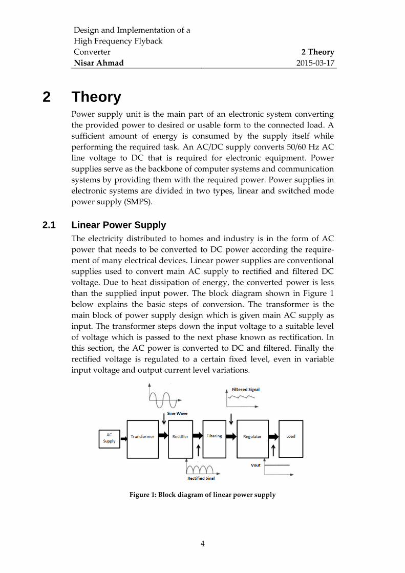
2 Theory Power supply unit is the main part of an electronic system converting
the provided power to desired or usable form to the connected load. A
sufficient amount of energy is consumed by the supply itself while
performing the required task. An AC/DC supply converts 50/60 Hz AC
line voltage to DC that is required for electronic equipment. Power
supplies serve as the backbone of computer systems and communication
systems by providing them with the required power. Power supplies in
electronic systems are divided in two types, linear and switched mode
power supply (SMPS).
2.1 Linear Power Supply
The electricity distributed to homes and industry is in the form of AC
power that needs to be converted to DC power according the require-
ment of many electrical devices. Linear power supplies are conventional
supplies used to convert main AC supply to rectified and filtered DC
voltage. Due to heat dissipation of energy, the converted power is less
than the supplied input power. The block diagram shown in Figure 1
below explains the basic steps of conversion. The transformer is the
main block of power supply design which is given main AC supply as
input. The transformer steps down the input voltage to a suitable level
of voltage which is passed to the next phase known as rectification. In
this section, the AC power is converted to DC and filtered. Finally the
rectified voltage is regulated to a certain fixed level, even in variable
input voltage and output current level variations.
Figure 1: Block diagram of linear power supply
Design and Implementation of a
High Frequency Flyback
Converter
Nisar Ahmad
2 Theory
2015-03-17
5
2.2 Switched Mode Power Supply
Considering the multiple DC voltage levels required by many electronic
devices, designers need a way to convert the standard power source
potentials into the voltages dictated by the load [2]. The voltage level
required by the attached load requires a system that could provide
regulated supply at an appropriate level, and this conversion should be
made through an efficient process. The latest technology devices de-
signed to perform efficiently in different areas require a reliable power
source. Switched mode power supplies are designed to convert supplied
AC or DC to an appropriate DC level, mostly for applications requiring
low power. Unlike linear regulators they are low in cost, suitable in size
and weight with high overall performance. A block diagram of a
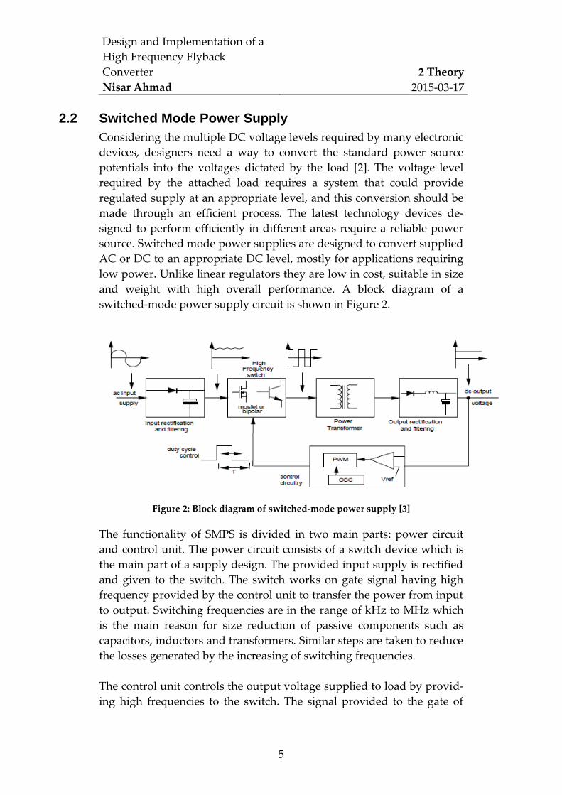
switched-mode power supply circuit is shown in Figure 2.
Figure 2: Block diagram of switched-mode power supply [3]
The functionality of SMPS is divided in two main parts: power circuit
and control unit. The power circuit consists of a switch device which is
the main part of a supply design. The provided input supply is rectified
and given to the switch. The switch works on gate signal having high
frequency provided by the control unit to transfer the power from input
to output. Switching frequencies are in the range of kHz to MHz which
is the main reason for size reduction of passive components such as
capacitors, inductors and transformers. Similar steps are taken to reduce
the losses generated by the increasing of switching frequencies.
The control unit controls the output voltage supplied to load by provid-
ing high frequencies to the switch. The signal provided to the gate of
Design and Implementation of a
High Frequency Flyback
Converter
Nisar Ahmad
2 Theory
2015-03-17
6
switch is a pulse width modulated (PWM) signal having a frequency
that decides the switch’s ON and OFF duration.
2.3 DC-DC Power Converter
Power converters play an important role in converting supplied power
to the required power by circuits. The power requirement of the latest
technology devices that mostly contain sub-circuits need to be fulfilled
efficiently due to their own separate voltage requirement. The source of
power supplied to laptop computers and cellular phones are batteries,
and this supplied power is further converted to an appropriate level
according the requirement of the sub-circuits performing separate
operations. DC to DC power converters make an electronic circuit used
to convert one DC voltage level to another. In the following sections, DC
to DC converters and its types are explained in detail.
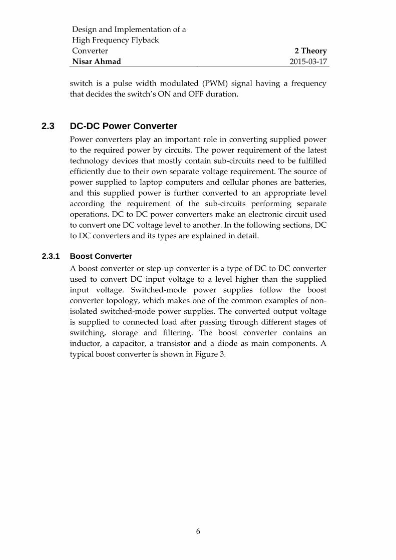
2.3.1 Boost Converter
A boost converter or step-up converter is a type of DC to DC converter
used to convert DC input voltage to a level higher than the supplied
input voltage. Switched-mode power supplies follow the boost
converter topology, which makes one of the common examples of non-
isolated switched-mode power supplies. The converted output voltage
is supplied to connected load after passing through different stages of
switching, storage and filtering. The boost converter contains an
inductor, a capacitor, a transistor and a diode as main components. A
typical boost converter is shown in Figure 3.
Design and Implementation of a
High Frequency Flyback
Converter
Nisar Ahmad
2 Theory
2015-03-17
7
Figure 3: Boost converter basic schematic with parasitics [4]
When the switch is closed the diode acts as a reverse biased resulting in
an open circuit. In this state, no current is flowing due to the open circuit
and output capacitor providing energy to the load. The working
principle of the boost converter is same as the flyback converter. The
energy is stored during the ON-time of the switch and delivered to load
during the OFF-time. When the switch is in OFF-state, the diode acts as
a forward biased to provide the energy stored in the previous ON-cycle.
The relation between input and output voltages are explained in the
simplified equation below.
VinD
Vout
)1
1(
(1)
The output voltage is delivered to the load depending on the duty cycle
‚D‛ which decides the ON and OFF intervals of the switch. In Figure 3
above, parasitics related to the passive components are included.
Design and Implementation of a
High Frequency Flyback
Converter
Nisar Ahmad
2 Theory
2015-03-17
8
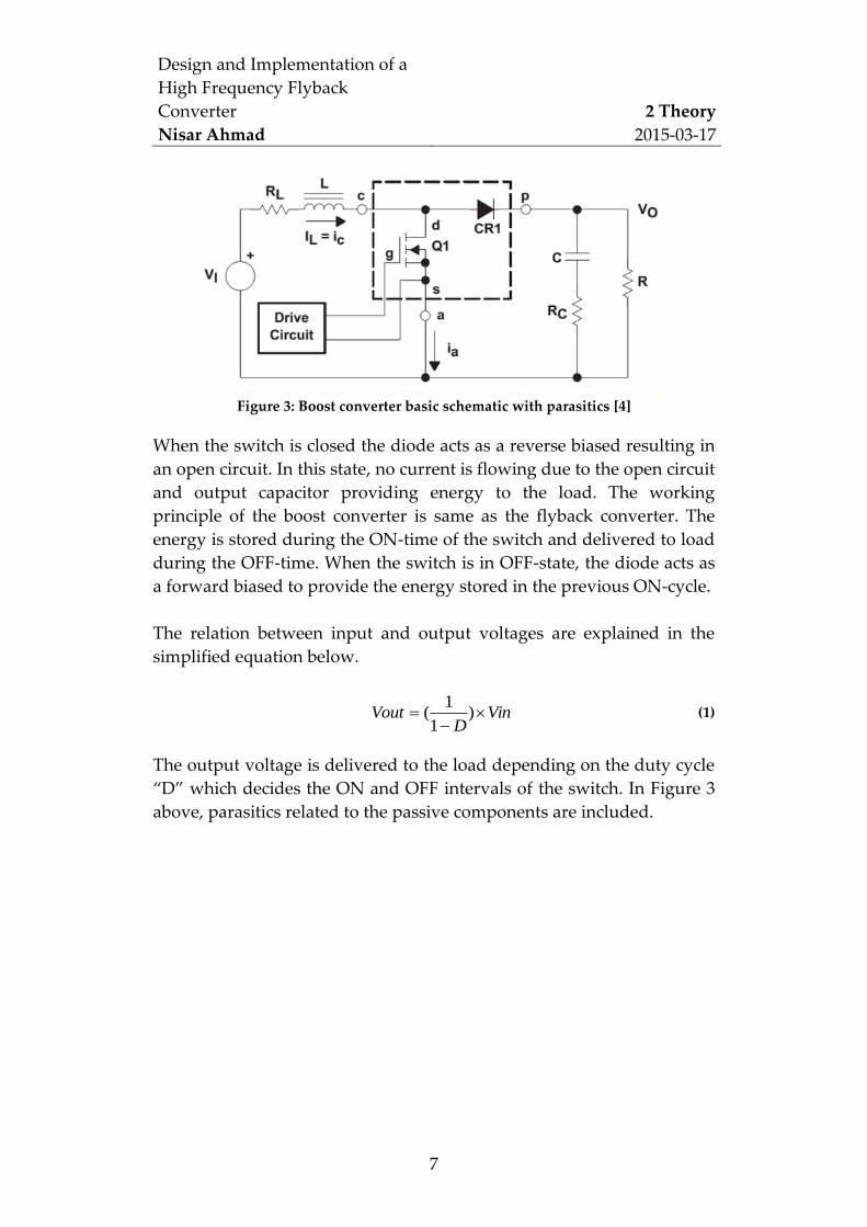
2.3.2 Buck Converter
Switched mode power supplies are based on buck converter topology
when high input voltages are intended to be converted to low output
voltage. A buck converter is also a non-isolated converter like a boost
converter and known as a step-down converter due to its ability to
convert high input voltage to low output voltage. A typical buck
converter is displayed in Figure 4.
Figure 4: A buck converter basic schematic [5]
The equivalent series resistance due to capacitor C and DC resistance
due to inductor L shown in the figure are included for analysis. The
switch Q1 provides current to the load depending on the switching
states ON and OFF. Due to the switching phenomenon low amount of
energy is dissipated in the switch. When switch Q1 is ON, the current to
the load is provided by inductor L. The current at the inductor rises
linearly due to the supplied voltage. This rise in current is explained in
the following equation [6],
L
VoVi
T
I
(2)
The current provided by inductor L undergoes a smoothing process by
capacitor C, hence converting the provided current into smooth voltage
provided to the load. In this cycle, diode D1 acts as a reverse biased that
leads to an open circuit, and no diode is considered in equivalent circuit.
In the OFF-state the inductor continues providing current to the load
until the inductor current falls after the magnetic field collapses. The
following equation describes the current fall:
Design and Implementation of a
High Frequency Flyback
Converter
Nisar Ahmad
2 Theory
2015-03-17
9
L
VDVi
T
I 1
(3)
The voltage across the inductor is reversed in this cycle. Diode D1 starts
conduction as forward biasing and provides a path to the inductor
current.
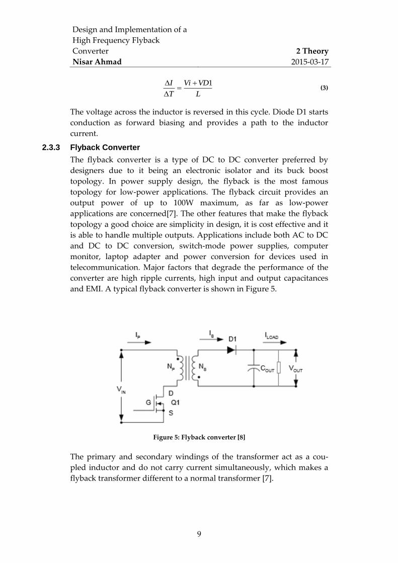
2.3.3 Flyback Converter
The flyback converter is a type of DC to DC converter preferred by
designers due to it being an electronic isolator and its buck boost
topology. In power supply design, the flyback is the most famous
topology for low-power applications. The flyback circuit provides an
output power of up to 100W maximum, as far as low-power
applications are concerned[7]. The other features that make the flyback
topology a good choice are simplicity in design, it is cost effective and it
is able to handle multiple outputs. Applications include both AC to DC
and DC to DC conversion, switch-mode power supplies, computer
monitor, laptop adapter and power conversion for devices used in
telecommunication. Major factors that degrade the performance of the
converter are high ripple currents, high input and output capacitances
and EMI. A typical flyback converter is shown in Figure 5.
Figure 5: Flyback converter [8]
The primary and secondary windings of the transformer act as a cou-
pled inductor and do not carry current simultaneously, which makes a
flyback transformer different to a normal transformer [7].
Design and Implementation of a
High Frequency Flyback
Converter
Nisar Ahmad
2 Theory
2015-03-17
10
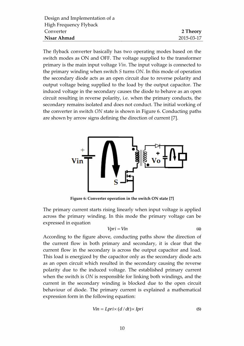
The flyback converter basically has two operating modes based on the
switch modes as ON and OFF. The voltage supplied to the transformer
primary is the main input voltage Vin. The input voltage is connected to
the primary winding when switch S turns ON. In this mode of operation
the secondary diode acts as an open circuit due to reverse polarity and
output voltage being supplied to the load by the output capacitor. The
induced voltage in the secondary causes the diode to behave as an open
circuit resulting in reverse polarity, i.e. when the primary conducts, the
secondary remains isolated and does not conduct. The initial working of
the converter in switch ON state is shown in Figure 6. Conducting paths
are shown by arrow signs defining the direction of current [7].
Figure 6: Converter operation in the switch ON state [7]
The primary current starts rising linearly when input voltage is applied
across the primary winding. In this mode the primary voltage can be
expressed in equation VinVpri (4)
According to the figure above, conducting paths show the direction of
the current flow in both primary and secondary, it is clear that the
current flow in the secondary is across the output capacitor and load.
This load is energized by the capacitor only as the secondary diode acts
as an open circuit which resulted in the secondary causing the reverse
polarity due to the induced voltage. The established primary current
when the switch is ON is responsible for linking both windings, and the
current in the secondary winding is blocked due to the open circuit
behaviour of diode. The primary current is explained a mathematical
expression form in the following equation:
IpridtdLpriVin )/( (5)
Design and Implementation of a
High Frequency Flyback
Converter
Nisar Ahmad
2 Theory
2015-03-17
11
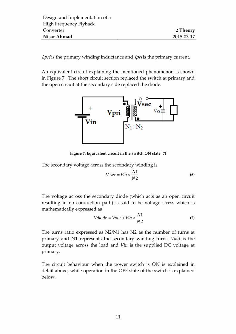
Lpri is the primary winding inductance and Ipri is the primary current.
An equivalent circuit explaining the mentioned phenomenon is shown
in Figure 7. The short circuit section replaced the switch at primary and
the open circuit at the secondary side replaced the diode.
Figure 7: Equivalent circuit in the switch ON state [7]
The secondary voltage across the secondary winding is
2
1sec
N
NVinV (6)
The voltage across the secondary diode (which acts as an open circuit
resulting in no conduction path) is said to be voltage stress which is
mathematically expressed as
2
1
N
NVinVoutVdiode (7)
The turns ratio expressed as N2/N1 has N2 as the number of turns at
primary and N1 represents the secondary winding turns. Vout is the
output voltage across the load and Vin is the supplied DC voltage at
primary.
The circuit behaviour when the power switch is ON is explained in
detail above, while operation in the OFF state of the switch is explained
below.
Design and Implementation of a
High Frequency Flyback
Converter
Nisar Ahmad
2 Theory
2015-03-17
12
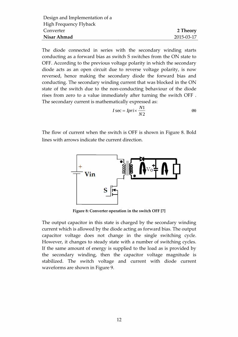
The diode connected in series with the secondary winding starts
conducting as a forward bias as switch S switches from the ON state to
OFF. According to the previous voltage polarity in which the secondary
diode acts as an open circuit due to reverse voltage polarity, is now
reversed, hence making the secondary diode the forward bias and
conducting. The secondary winding current that was blocked in the ON
state of the switch due to the non-conducting behaviour of the diode
rises from zero to a value immediately after turning the switch OFF .
The secondary current is mathematically expressed as:
2
1sec
N
NIpriI (8)
The flow of current when the switch is OFF is shown in Figure 8. Bold
lines with arrows indicate the current direction.
Figure 8: Converter operation in the switch OFF [7]
The output capacitor in this state is charged by the secondary winding
current which is allowed by the diode acting as forward bias. The output
capacitor voltage does not change in the single switching cycle.
However, it changes to steady state with a number of switching cycles.
If the same amount of energy is supplied to the load as is provided by
the secondary winding, then the capacitor voltage magnitude is
stabilized. The switch voltage and current with diode current
waveforms are shown in Figure 9.
Design and Implementation of a
High Frequency Flyback
Converter
Nisar Ahmad
2 Theory
2015-03-17
13
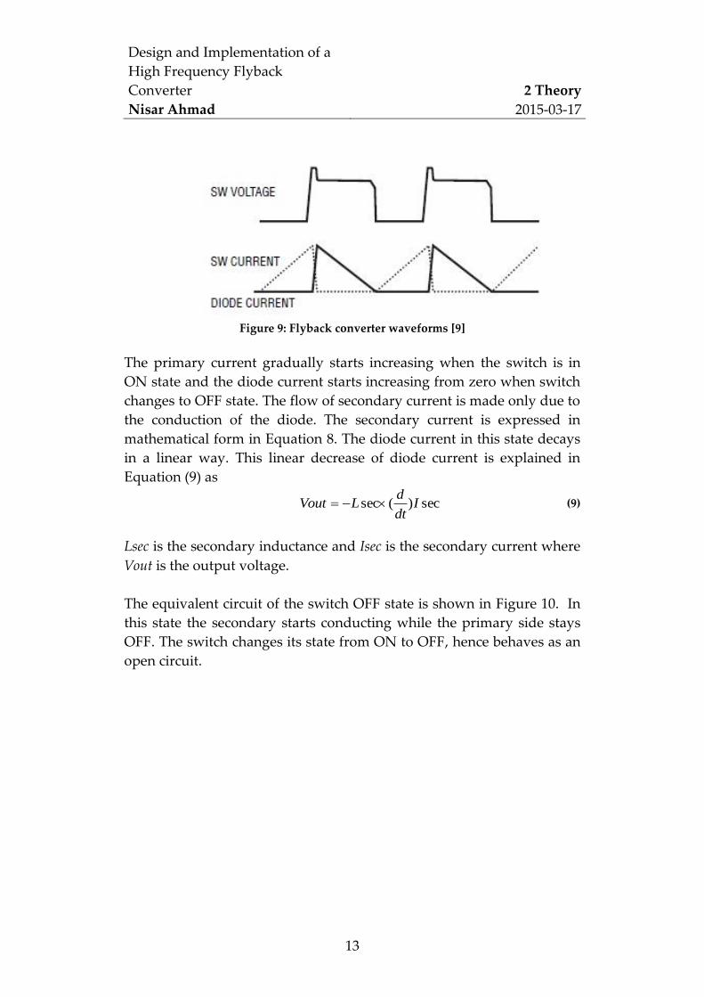
Figure 9: Flyback converter waveforms [9]
The primary current gradually starts increasing when the switch is in
ON state and the diode current starts increasing from zero when switch
changes to OFF state. The flow of secondary current is made only due to
the conduction of the diode. The secondary current is expressed in
mathematical form in Equation 8. The diode current in this state decays
in a linear way. This linear decrease of diode current is explained in
Equation (9) as
sec)(sec Idt
dLVout (9)
Lsec is the secondary inductance and Isec is the secondary current where
Vout is the output voltage.
The equivalent circuit of the switch OFF state is shown in Figure 10. In
this state the secondary starts conducting while the primary side stays
OFF. The switch changes its state from ON to OFF, hence behaves as an
open circuit.
Design and Implementation of a
High Frequency Flyback
Converter
Nisar Ahmad
2 Theory
2015-03-17
14
Figure 10: Equivalent circuit in switch OFF state
The diode at the secondary starts conducting and is replaced by a short
circuit in the figure. The bold section of in the figure shows the
conduction path. Switch voltage in this state is the sum of input voltage
and reflected back output voltage and measured as drain to source
voltage across switch. Typical waveform of switch voltage is shown in
the figure and expressed in the equation as
)2
1(N
NVoutVinVsw (10)
Design and Implementation of a
High Frequency Flyback
Converter
Nisar Ahmad
2 Theory
2015-03-17
15
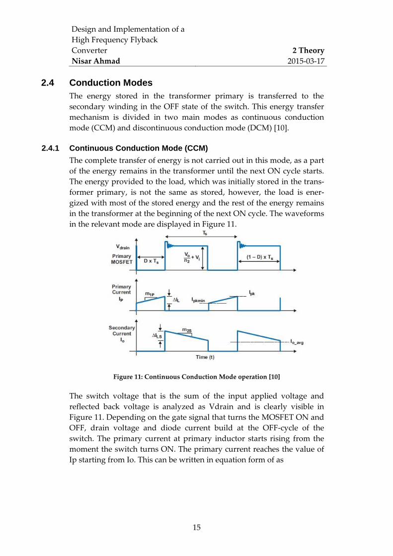
2.4 Conduction Modes
The energy stored in the transformer primary is transferred to the
secondary winding in the OFF state of the switch. This energy transfer
mechanism is divided in two main modes as continuous conduction
mode (CCM) and discontinuous conduction mode (DCM) [10].
2.4.1 Continuous Conduction Mode (CCM)
The complete transfer of energy is not carried out in this mode, as a part
of the energy remains in the transformer until the next ON cycle starts.
The energy provided to the load, which was initially stored in the trans-
former primary, is not the same as stored, however, the load is ener-
gized with most of the stored energy and the rest of the energy remains
in the transformer at the beginning of the next ON cycle. The waveforms
in the relevant mode are displayed in Figure 11.
Figure 11: Continuous Conduction Mode operation [10]
The switch voltage that is the sum of the input applied voltage and
reflected back voltage is analyzed as Vdrain and is clearly visible in
Figure 11. Depending on the gate signal that turns the MOSFET ON and
OFF, drain voltage and diode current build at the OFF-cycle of the
switch. The primary current at primary inductor starts rising from the
moment the switch turns ON. The primary current reaches the value of
Ip starting from Io. This can be written in equation form of as
Design and Implementation of a
High Frequency Flyback
Converter
Nisar Ahmad
2 Theory
2015-03-17
16
)()( TDLpri
VinIoIp (11)
The duty cycle represented as D where T is the time period of the
switching cycle. The reflected secondary voltage measured when the
switch is in the OFF-state is described in an equation with relation to
output voltage, turns ratio and duty cycle.
)1()2
( DVoN
NiDVin (12)
The output voltage can be can be simplified as,
)1
()1
(ND
DVinVo
(13)
Similarly, the duty cycle from the equation above can be equated as,
Vin
DVoN
N
D
)1()2
1(
(14)
The relation is the reflected secondary voltage at primary
winding measured when the switch is OFF. The inductance value in the
CCM operations is large, however, the ripple current value is small [10].
2.4.2 Discontinuous Conduction Mode (DCM)
In this energy transfer mode when MOSFET turns ON, the primary
current starts rising from zero to peak value. The peak current in DCM
could be twice or more to CCM peak current. Following the same steps
of energy storage mechanism as CCM, energy is stored in the primary
winding until the switch is in the ON-state. During the switch’s OFF-
period, complete transfer of energy is made, which was stored during
the ON-state. From Figure 12, it is clear that the secondary current goes
to zero until next the ON-cycle appears [10].
Design and Implementation of a
High Frequency Flyback
Converter
Nisar Ahmad
2 Theory
2015-03-17
17
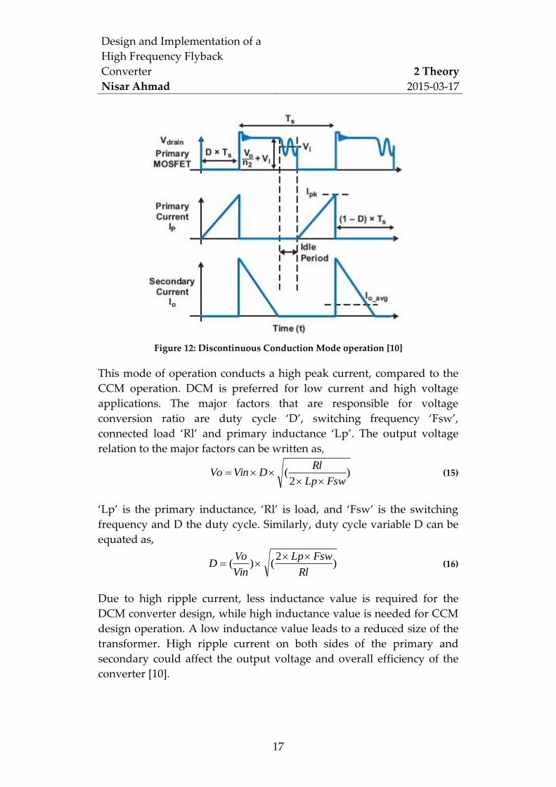
Figure 12: Discontinuous Conduction Mode operation [10]
This mode of operation conducts a high peak current, compared to the
CCM operation. DCM is preferred for low current and high voltage
applications. The major factors that are responsible for voltage
conversion ratio are duty cycle ‘D’, switching frequency ‘Fsw’,
connected load ‘Rl’ and primary inductance ‘Lp’. The output voltage
relation to the major factors can be written as,
)2
(FswLp
RlDVinVo
(15)
‘Lp’ is the primary inductance, ‘Rl’ is load, and ‘Fsw’ is the switching
frequency and D the duty cycle. Similarly, duty cycle variable D can be
equated as,
)2
()(Rl
FswLp
Vin
VoD
(16)
Due to high ripple current, less inductance value is required for the
DCM converter design, while high inductance value is needed for CCM
design operation. A low inductance value leads to a reduced size of the
transformer. High ripple current on both sides of the primary and
secondary could affect the output voltage and overall efficiency of the
converter [10].

Design and Implementation of a
High Frequency Flyback
Converter
Nisar Ahmad
2 Theory
2015-03-17
18
2.5 Switching Techniques
The operation of a flyback converter depends on the switching
technique adopted, which is responsible for the performance, behaviour
and efficiency of the converter. Switching techniques followed by the
converters are categorized as hard switching and soft switching.
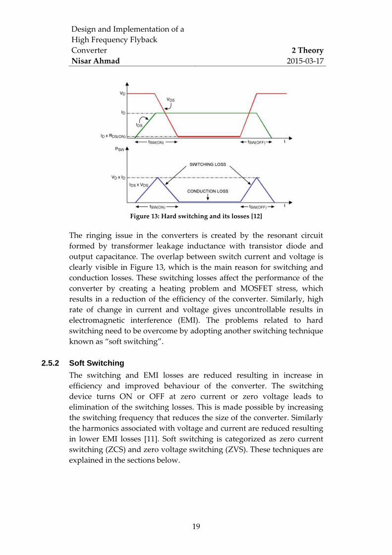
2.5.1 Hard Switching
PWM converters are conventionally operated in the hard switching
technique. The overlap between MOSFET current and voltage during
the transition state from ON to OFF and vice versa is known as hard-
switching, and a converter operated in this mode is said to be a hard
switched converter.
2.5.1.1 Hard Switching Issues
In this method abrupt change in current and voltages from highest to
lowest value and vice versa associated to switch generate switching
losses and interference. The parasitics involved in switching losses are
transistor output capacitance, transformer leakage inductance, diode
reverse recovery and diode capacitance. The transistor output
capacitance energy before the transistor turns ON can be expressed as
[11],
2)2
1( VoffCoWco (17)
Wco is referred to as output capacitance and Voff is the switch OFF-state
voltage. The energy stored in output capacitance of the switch equated
in Equation 17 relates to the OFF-period of the switch. This energy is
converted to switch loss when switch turns ON and Equation 17 can be
simplified as,
FswVoffCoPsw 2)2
1( (18)
Fsw is the switching frequency. Hard switching behaviour and switching
losses are shown in Figure 13.
Design and Implementation of a
High Frequency Flyback
Converter
Nisar Ahmad
2 Theory
2015-03-17
19
Figure 13: Hard switching and its losses [12]
The ringing issue in the converters is created by the resonant circuit
formed by transformer leakage inductance with transistor diode and
output capacitance. The overlap between switch current and voltage is
clearly visible in Figure 13, which is the main reason for switching and
conduction losses. These switching losses affect the performance of the
converter by creating a heating problem and MOSFET stress, which
results in a reduction of the efficiency of the converter. Similarly, high
rate of change in current and voltage gives uncontrollable results in
electromagnetic interference (EMI). The problems related to hard
switching need to be overcome by adopting another switching technique
known as ‚soft switching‛.
2.5.2 Soft Switching
The switching and EMI losses are reduced resulting in increase in
efficiency and improved behaviour of the converter. The switching
device turns ON or OFF at zero current or zero voltage leads to
elimination of the switching losses. This is made possible by increasing
the switching frequency that reduces the size of the converter. Similarly
the harmonics associated with voltage and current are reduced resulting
in lower EMI losses [11]. Soft switching is categorized as zero current
switching (ZCS) and zero voltage switching (ZVS). These techniques are
explained in the sections below.
Design and Implementation of a
High Frequency Flyback
Converter
Nisar Ahmad
2 Theory
2015-03-17
20
2.5.2.1 Zero Current Switching
In ZCS technique the switch turns ON and OFF at zero current. As the
device turns ON or OFF at zero current the product of the device
voltage and current during transition is zero, which eliminates the
switching losses. The current waveforms are smoothened by
introducing resonant elements, networks having a capacitor ‘C’ and
inductor ‘L’ [13].
2.5.2.2 Zero Voltage Switching
Turning the switch ON at higher voltages generates switching noise
which results in high noise generation and switch circuitry problems. In
ZVS the switch turns ON when the drain to source voltage reaches zero,
which is also said to be zero voltage switching [13]. To obtain the con-
verters working on ZVS technique, resonant capacitor Cr is connected in
parallel to the switch and resonant inductor Lr in series with the parallel
circuit of capacitor and switch. The resonant capacitor Cr absorbs the
output capacitance Co which causes ripples in combination with the
primary leakage inductance. The power MOSFET itself contains an
antiparallel diode which blocks the negative voltage by less than -0.7V.
As the switch allows only voltage in one direction and blocks the nega-
tive voltage until it reaches the specified level, therefore this switch acts
as unidirectional for voltage and bidirectional for current [11]. This
methodology is preferred for high frequency applications. The parasitic
capacitance across the switch stores energy when the switch is OFF and
releases this stored energy during the ON-cycle. This issue of interfer-
ence is solved using the ZVS converters at high frequencies [14].
Design and Implementation of a
High Frequency Flyback
Converter
Nisar Ahmad
3 Related Work
2015-03-17
21
3 Related Work The flyback converter has been implemented using different methods
depending on application. The converter applications relevant for cur-
rent thesis work are presented here.
Zhang et al [15] found that during the on-time of the switch energy is
stored in magnetizing inductance, which is completely discharged when
the switch is off. Secondary current is observed to reach zero before the
starting of the switch. Measurement points for efficiency plots are col-
lected at valley points of drain voltage. In this application variable
frequency DCM flyback converter was perceived as suitable for syn-
chronous rectification, and efficiency improvement of 2% to 4% was
observed. Converter applications have been made using a universal
input voltage range with an output of 15V/36W flyback prototype.
H.B. Kotte et al [16] implemented a ZVS flyback converter application
by using a coreless multilayer printed circuit board (PCB) step-down
power transformer. Converter losses are minimized using ZVS tech-
nique to improve the performance of the converter, which makes soft
switching more suitable compared to a hard switched converter. Input
voltage varies from 25V to 40V DC and the output power of the con-
verter is adjusted to 10W. The converter is switched in a range of high
frequencies in the range of 2.7MHz to 4.3MHz. Output voltage and
power are maintained to 13V and 5.7W while varying the input voltage.
Another application includes design guidelines for the flyback converter
for the next generation of high power density adapter applications. L
Huber and M. M Jovanovic [17] worked on the Notebook AC/DC
adapter/charger application. Mathcad based design optimization soft-
ware tool is used in the design process. Analytical based analysis and
design optimization tools are required to fulfil the component loss
estimation due to the small value of output power. The flyback topology
in this design is preferred due to its low component count and it being
suitable in low-power applications. The software helped to calculate the
loss components, such as switching losses, output filter loss, secondary
side losses and transformer core/copper losses. High break down volt-
age 600V power MOSFET is used in the application. From experimental
results maximum drain to source voltage was observed as 550V with
Design and Implementation of a
High Frequency Flyback
Converter
Nisar Ahmad
3 Related Work
2015-03-17
22
385VDC input voltage range. The efficiency in DCM while operating in
the RCD clamp circuit is observed as suitable. In lower switching fre-
quencies, the RCD clamp flyback charger/adapter are suggested as
efficient, however, in the higher frequency range of 300-500 KHz, active
clamp flyback topology is suggested.
To achieve efficient and high power density converters, the use of high
power density transformers and their applications in the high frequency
range has become inevitable. The increase in switching frequency leads
to avoidable increase in a series of losses in form of copper losses, core
losses and dielectric losses. These parasitic elements badly affect the
performance of converters, hence reducing the efficiency at the end. To
remove the losses that are the causes of performance and efficiency
degrading, a transformer having minimum copper and core loss has to
be designed. Hari Babu Kotte et al [18] implemented a series resonant
converter using a multilayer coreless PCB transformer. The design
characteristics of the multilayer PCB transformer and its applications in
research work have been presented briefly. The alteration in design
parameters to achieve the desired goal is at best a part of research in
power electronics. The switching frequency range used in conventional
converters is in hundreds of kHz. The reason for this limitation to the
kHz range is non-availability of high energy efficient transformers.
Hybrid power transformer with an efficiency of 98% to be operated in
the frequency range from 3 to 5MHz has been designed, which could be
used in power transfer applications up to 50W. The transformer core is
designed to increase the frequency application range to 10MHz.
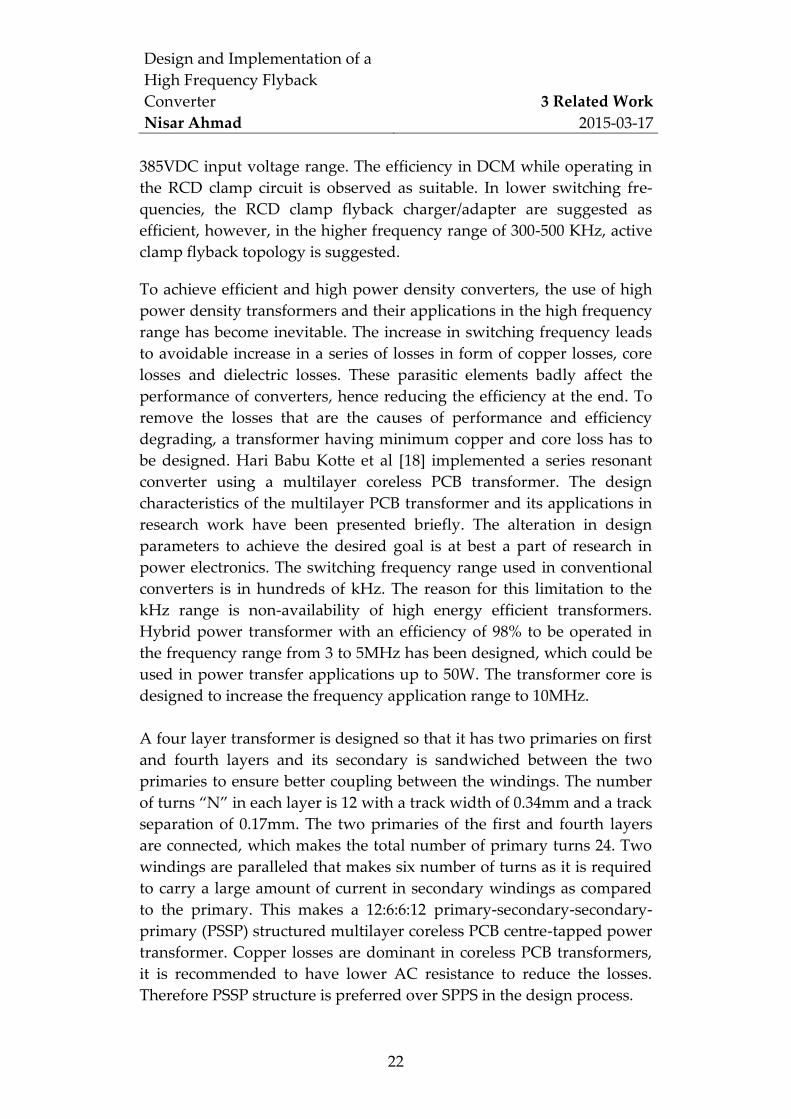
A four layer transformer is designed so that it has two primaries on first
and fourth layers and its secondary is sandwiched between the two
primaries to ensure better coupling between the windings. The number
of turns ‚N‛ in each layer is 12 with a track width of 0.34mm and a track
separation of 0.17mm. The two primaries of the first and fourth layers
are connected, which makes the total number of primary turns 24. Two
windings are paralleled that makes six number of turns as it is required
to carry a large amount of current in secondary windings as compared
to the primary. This makes a 12:6:6:12 primary-secondary-secondary-
primary (PSSP) structured multilayer coreless PCB centre-tapped power
transformer. Copper losses are dominant in coreless PCB transformers,
it is recommended to have lower AC resistance to reduce the losses.
Therefore PSSP structure is preferred over SPPS in the design process.
Design and Implementation of a
High Frequency Flyback
Converter
Nisar Ahmad
3 Related Work
2015-03-17
23
Cross-sectional view and 3D view of planar transformer is shown in
Figure 14.
Figure 14: (a) Cross-sectional view and 3D view of coreless PCB transformer. (b)
Three dimensional view of multilayer coreless PCB power transformer PSSP
structure [18]
Table 1: Transformer Construction Parameters
Height of copper
Track
Thickness of
substrate
Inner
radius
Outer
radius
70um 0.4mm 4.5mm 10mm
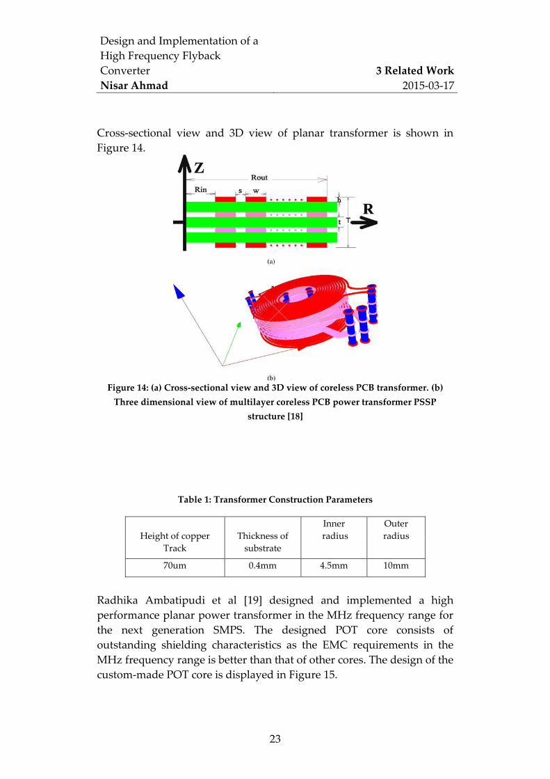
Radhika Ambatipudi et al [19] designed and implemented a high
performance planar power transformer in the MHz frequency range for
the next generation SMPS. The designed POT core consists of
outstanding shielding characteristics as the EMC requirements in the
MHz frequency range is better than that of other cores. The design of the
custom-made POT core is displayed in Figure 15.

Design and Implementation of a
High Frequency Flyback
Converter
Nisar Ahmad
3 Related Work
2015-03-17
24
Figure 15: POT core design [19]
The dimensions of the designed POT core are displayed in Table 2. The
parameters are distance (d1, d2, d3), length (l), height (h1, h2), centre (c),
over all diameter (D1) and height (H1), effective length and area of cross
section as le and Ae and core volume as Ve.
Table 2: Dimensions of the designed POT core
Dimensions of the designed POT core
Distance(mm) Height(mm) Length
l(mm)
Centre
c(mm)
D1(mm) H1(mm) Le(mm) Ae(mm²) Ve(mm³)
d1 d2 d3 h1 h2
16 14 6 2.5 1.2 4 3 16 2.5 15.3 30.3 464
A multi-layer planar PCB transformer with POT core showing top and
bottom views are displayed in Figure 16. The designed planar
transformer is the main component of the converter circuit whose
primary is connected to components having common ground, and the
secondary is providing the converted voltage to the load having
separate ground.

Design and Implementation of a
High Frequency Flyback
Converter
Nisar Ahmad
3 Related Work
2015-03-17
25
Figure 16: Multilayer PCB Transformer (centre) with POT core
Design and Implementation of a
High Frequency Flyback
Converter
Nisar Ahmad
4 Methodology/Model
2015-03-17
26
4 Methodology/Model To accomplish the main goals of the thesis, different methods are adopt-
ed. The main three methods adapted to design and implement the
converter are categorized as background study of converters and theo-
retical calculations to design the circuitry for converter, PCB design and
implementation by integrating converter using planar transformer and
controlling the switch.
4.1 Converter Circuit Design
The theory and concepts related to the SMPS and flyback converter are
covered as the first step of thesis. The converter circuitry is designed by
dividing the circuit in main modules such as power supply section,
control section, switching circuitry and planar transformer circuit sec-
tion. These sections contain a network of components and values for
these components are selected by theoretical calculations.
4.2 PCB Design for Converter
Designing the two layer-PCB for the converter is the main and first step
toward project accomplishment. This design includes the separate
power supplies for the gate driver IC and the transformer. For this
purpose, two separate connectors are placed in the design. The supplied
input voltage from both power supplies need to be filtered before ener-
gizing the components. The output load is selected with maximum
power handling capability. In the design the switch is the main compo-
nent that needs to be operated safely to avoid device failure. The con-
troller selection needs to fulfil high switching frequency and voltage and
current mode control for feedback applications. The component selec-
tion is made based on size compactness, cost effectiveness and perfor-
mance.
4.3 Switch Control using dsPIC Processor
The control section handles the operations of the system by generating a
control signal that drives the switch. Therefore an appropriate control
signal is required to drive the system to achieve the desired conduction
mode. It consists of a digital signal processor (DSP) and a MOSFET gate
driver that makes the control signal suitable as required by the switch.
The pulse width modulation (PWM) signals are generated by the micro-
Design and Implementation of a
High Frequency Flyback
Converter
Nisar Ahmad
4 Methodology/Model
2015-03-17
27
controller from the PWM channels having a resolution of 1.04ns. The
main attributes of the PWM signal such as duty cycle and frequency
needs to be altered from the microcontroller to achieve high frequency
switching. High frequency switching has become possible due to the
availability of the latest technology power MOSFET. The main purpose
of the thesis is to increase the range of input voltage that was previously
maintained at 70V. For this purpose the CoolMOS power MOSFET has
been selected due to benefits such as fast switching, low conduction and
switching losses, compactness and high breakdown voltages. The
MOSFET selected for the converter application is IPL60R385CP which
has breakdown voltage VDS of 650V and RDS(ON) of 0.385Ω [20].
4.4 Converter Integration by Utilizing Planar Transformer
The converter integration needs PCB component soldering, control
signal generation by programming and external power supplies connec-
tion (included in the design) which finally makes a system work. PWM
signal attributes such as frequency and voltage need to be analysed at
the microcontroller (PWM) pins. Planar PCB transformer is selected and
used in the converter design. Gate and drain voltage signals are the
main focus of analysis in this thesis. To operate the MOSFET safely and
avoiding switching losses, the duty cycle value needs to be kept low.
While working on a higher range of input voltages, the main problem
that occurs is overheating, which causes device failure. To avoid device
failure the temperature of the converter circuit needs to be analysed
using IR camera. The output parameters are measured and efficiency is
calculated by measuring values of output voltage Vout. A four-channel
oscilloscope is used to measure the waveforms. The signals measured
are input voltage (Vin), drain to source signal (Vds) and gate to source
signal (Vgs). Input power is calculated by multiplying two separately
measured values Vin and Iin. Output power is calculated by measuring
the output voltage across the load and dividing measured voltage by
load value.
Design and Implementation of a
High Frequency Flyback
Converter
Nisar Ahmad
5 Design and Implementation
2015-03-17
28
5 Design and Implementation The steps followed to design and implement the flyback converter are
presented in this chapter.
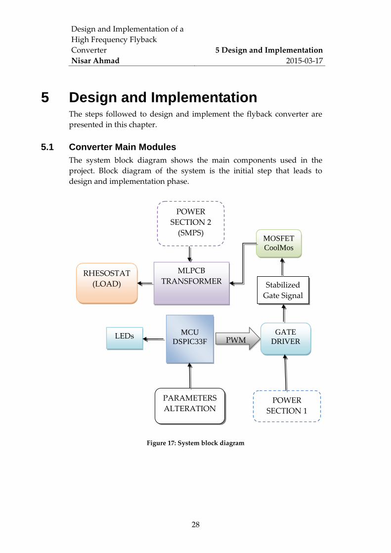
5.1 Converter Main Modules
The system block diagram shows the main components used in the
project. Block diagram of the system is the initial step that leads to
design and implementation phase.
Figure 17: System block diagram
GATE
DRIVER
MCU
DSPIC33F
MOSFET
CoolMos
MLPCB
TRANSFORMER
POWER
SECTION 2
(SMPS)
POWER
SECTION 1
RHESOSTAT
(LOAD)
PWM
Stabilized
Gate Signal
LEDs
PARAMETERS
ALTERATION

Design and Implementation of a
High Frequency Flyback
Converter
Nisar Ahmad
5 Design and Implementation
2015-03-17
29
5.2 Converter Hardware Design
In this section the flyback converter hardware components are present-
ed briefly with specifications.
5.2.1 dsPIC33FJ16GS502 Microcontroller
The microcontroller used in the project is a 16-bit Microchip
dsPIC33Fj16gs502. PIC microcontrollers are preferred in control applica-
tions due to certain features such as power efficient, faster and cheap. It
supports up to four PWM pairs with independent timing having a
resolution of 1.04ns. The various PWM modes supported by the micro-
controller are complementary, push pull, central aligned and true inde-
pendent mode. This microcontroller consists of advanced analog fea-
tures of high speed ADC module and flexible trigger configuration for
ADC conversions. It has PWM support for DC/DC, AC/DC, PFC, In-
verters and lighting applications. To operate the converter in the range
of high frequencies with stability, pic microcontroller is selected. In this
project 28 pins SOIC design is used and pin diagram is displayed in
Figure 18.
Figure 18: dsPIC33FJ16GS502 pin diagram [20]
5.2.2 Gate Driver
The transistor functionality basically depends on the gate drive signal
having sufficient voltage to turn the gate ON. The PWM signals gener-
ated by the microcontrollers do not contain the sufficient current value
required to turn it ON and work properly. This weak signal affects the
performance of the device by loss of power and slow switching. The
main drawbacks includes overheating and high current draw which
leads to the device malfunctioning and damage to the hardware. To
fulfill the requirement of switch drive and make the switch work

Design and Implementation of a
High Frequency Flyback
Converter
Nisar Ahmad
5 Design and Implementation
2015-03-17
30
properly we need a gate driver that accepts low power input from the
microcontroller and converts it to a suitable high current gate drive
signal required by the MOSFET [21]. The gate driver selection is made
by selecting LM5114 which is suitable for flyback applications. The pin
diagram is displayed in Figure 19. Each resistor is connected with
P_OUT and N_OUT pins that are finally connected to the gate of the
transistor by a single connection.
Figure 19: Gate driver LM5114 pin diagram [22]
5.2.3 CoolMOS IPL60R385CP Power MOSFET
The CoolMOS power transistors are preferred due to their high perfor-
mance, compactness and low switching losses. Other prominent features
that designers prefer are increased power density, smooth switching
waveforms and short commutation loop. The high breakdown voltage
of 650V in this MOSFET allows including this product in high voltage
applications. The MOSFET pin diagram and internal circuitry are dis-
played in Figure 20.
Figure 20: CoolMOS IPL60R385CP pin diagram [23]
Design and Implementation of a
High Frequency Flyback
Converter
Nisar Ahmad
5 Design and Implementation
2015-03-17
31
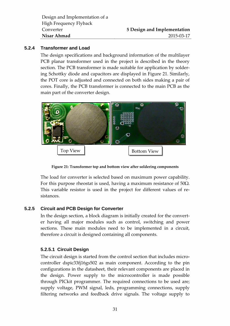
5.2.4 Transformer and Load
The design specifications and background information of the multilayer
PCB planar transformer used in the project is described in the theory
section. The PCB transformer is made suitable for application by solder-
ing Schottky diode and capacitors are displayed in Figure 21. Similarly,
the POT core is adjusted and connected on both sides making a pair of
cores. Finally, the PCB transformer is connected to the main PCB as the
main part of the converter design.
Figure 21: Transformer top and bottom view after soldering components
The load for converter is selected based on maximum power capability.
For this purpose rheostat is used, having a maximum resistance of 50Ω.
This variable resistor is used in the project for different values of re-
sistances.
5.2.5 Circuit and PCB Design for Converter
In the design section, a block diagram is initially created for the convert-
er having all major modules such as control, switching and power
sections. These main modules need to be implemented in a circuit,
therefore a circuit is designed containing all components.
5.2.5.1 Circuit Design
The circuit design is started from the control section that includes micro-
controller dspic33fj16gs502 as main component. According to the pin
configurations in the datasheet, their relevant components are placed in
the design. Power supply to the microcontroller is made possible
through PICkit programmer. The required connections to be used are;
supply voltage, PWM signal, leds, programming connections, supply
filtering networks and feedback drive signals. The voltage supply to
Top View Bottom View

Design and Implementation of a
High Frequency Flyback
Converter
Nisar Ahmad
5 Design and Implementation
2015-03-17
32
drive the IC is made optional as there were two supply connections:
internal and external. Internal voltage supply is made available through
programmer and externally, the power supply is connected to supply
5V that is dropped to the required 3.3V voltage by including two diodes
in series. Later, because of the gate drive high voltage requirement, an
external supply option to the MCU is removed to make it dedicated to
the gate driver, leaving the only internal supply an option for the MCU.
Figure 22: MCU power supply connection
The filtering capacitor C12 is included to remove high frequency com-
ponents. The PWM signal is generated to feed the gate driver to make it
suitable for the switch, to improve switching. The pin selection for the
PWM source is displayed in Figure 23.
Figure 23: PWM pin selection
In the design two leds are placed to verify the PWM signal generated.
These leds will glow when a PWM signal is generated. As there is only
one PWM source, PWM1L on led is dedicated for this purpose. Circuit
diagram for leds is displayed in Figure 24.
Design and Implementation of a
High Frequency Flyback
Converter
Nisar Ahmad
5 Design and Implementation
2015-03-17
33
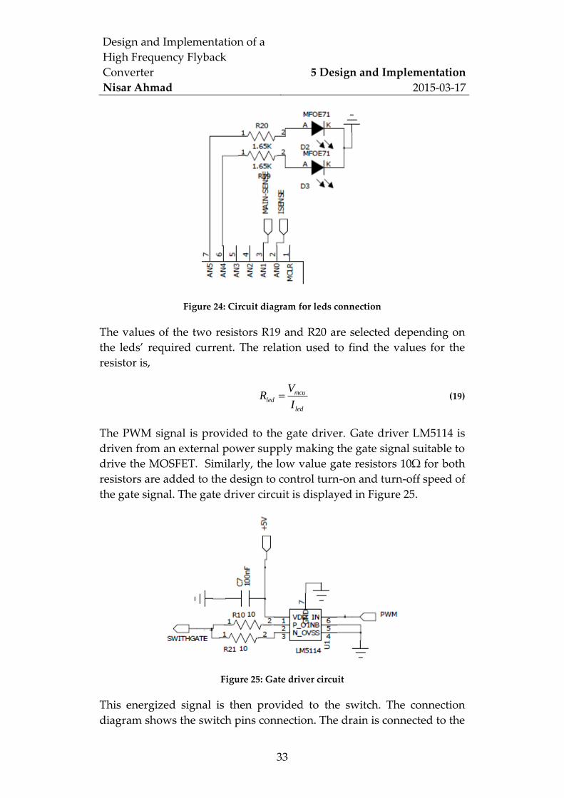
Figure 24: Circuit diagram for leds connection
The values of the two resistors R19 and R20 are selected depending on
the leds’ required current. The relation used to find the values for the
resistor is,
led
mculed
I
VR (19)
The PWM signal is provided to the gate driver. Gate driver LM5114 is
driven from an external power supply making the gate signal suitable to
drive the MOSFET. Similarly, the low value gate resistors 10Ω for both
resistors are added to the design to control turn-on and turn-off speed of
the gate signal. The gate driver circuit is displayed in Figure 25.
Figure 25: Gate driver circuit
This energized signal is then provided to the switch. The connection
diagram shows the switch pins connection. The drain is connected to the

Design and Implementation of a
High Frequency Flyback
Converter
Nisar Ahmad
5 Design and Implementation
2015-03-17
34
transformer primary side. The gate of MOSFET is connected to the gate
driver. The circuit diagram is shown in Figure 26. Resistor R9 is the
shunt resistor used to pass maximum current. The value for this resistor
is selected using Equation 21 and the low value resistor is placed.
Figure 26: MOSFET circuit for converter
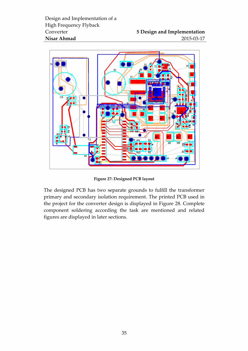
5.2.5.2 PCB Design
In the converter design phase, a two-layer PCB is designed to fulfil the
project requirements. The layout is displayed in Figure 27. Starting with
the microcontroller unit, a 28-pin small outline integrated circuit (SOIC)
is preferred due to its size compactness, compared to a dual inline
package (DIP).
Design and Implementation of a
High Frequency Flyback
Converter
Nisar Ahmad
5 Design and Implementation
2015-03-17
35
Figure 27: Designed PCB layout
The designed PCB has two separate grounds to fulfill the transformer
primary and secondary isolation requirement. The printed PCB used in
the project for the converter design is displayed in Figure 28. Complete
component soldering according the task are mentioned and related
figures are displayed in later sections.
Design and Implementation of a
High Frequency Flyback
Converter
Nisar Ahmad
5 Design and Implementation
2015-03-17
36
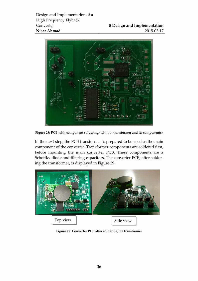
Figure 28: PCB with component soldering (without transformer and its components)
In the next step, the PCB transformer is prepared to be used as the main
component of the converter. Transformer components are soldered first,
before mounting the main converter PCB. These components are a
Schottky diode and filtering capacitors. The converter PCB, after solder-
ing the transformer, is displayed in Figure 29.
Figure 29: Converter PCB after soldering the transformer
Top view Side view
Design and Implementation of a
High Frequency Flyback
Converter
Nisar Ahmad
5 Design and Implementation
2015-03-17
37
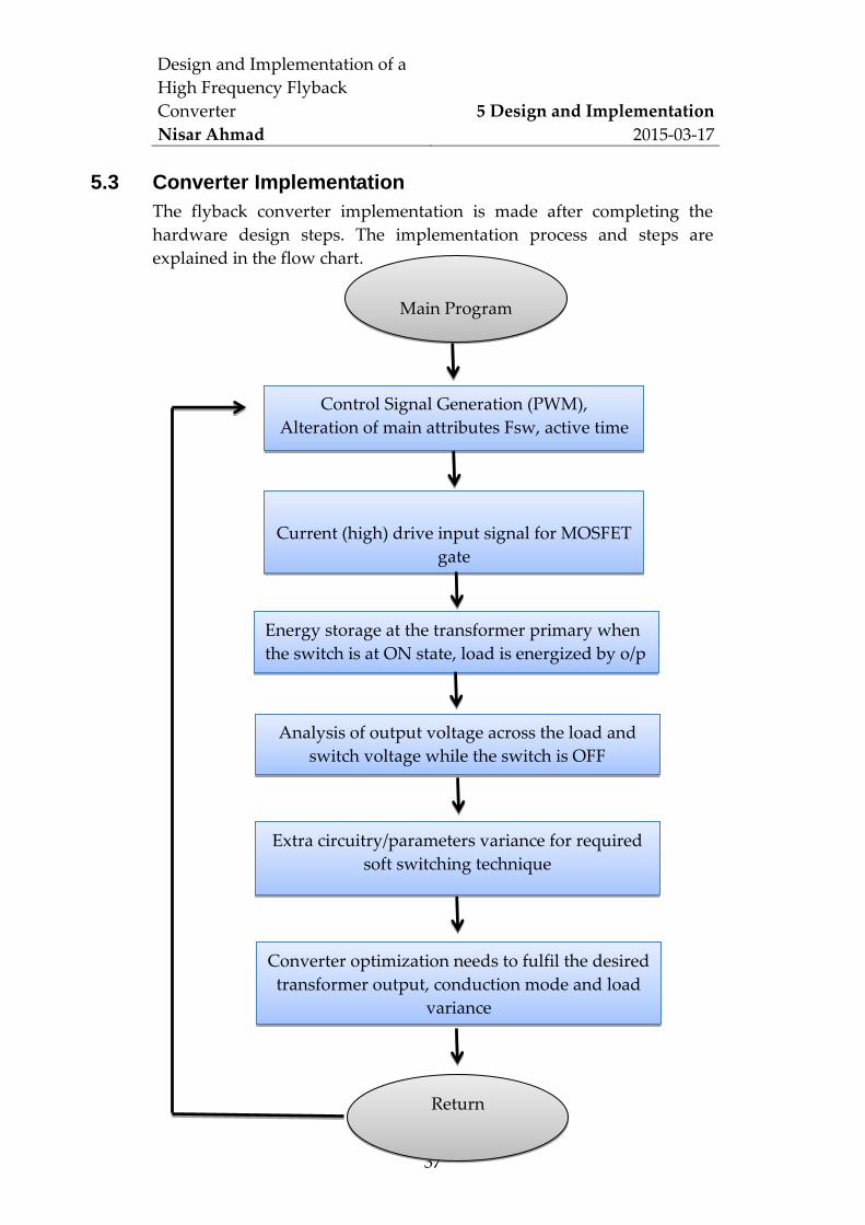
5.3 Converter Implementation
The flyback converter implementation is made after completing the
hardware design steps. The implementation process and steps are
explained in the flow chart.
Control Signal Generation (PWM),
Alteration of main attributes Fsw, active time
Current (high) drive input signal for MOSFET
gate
Energy storage at the transformer primary when
the switch is at ON state, load is energized by o/p
Cap.
Analysis of output voltage across the load and
switch voltage while the switch is OFF
Converter optimization needs to fulfil the desired
transformer output, conduction mode and load
variance
Return
Main Program
Extra circuitry/parameters variance for required
soft switching technique

Design and Implementation of a
High Frequency Flyback
Converter
Nisar Ahmad
5 Design and Implementation
2015-03-17
38
5.3.1 Gate Driver Signal
Software programmer and debugger PICkit 3 is used to program the
microcontroller. This debugger is controlled by the MPLAB program-
ming software which provides an environment in which to write a
program for the microcontroller. This six-pin debugger is connected to
the converter PCB by a six-pin connecter and the power option for the
controller is selected to be provided by the debugger. Therefore, the
controller is energized by the debugger. Starting with dsPIC program-
ing step, PWM pulse is generated from the microcontroller. The
MOSFET gate is driven by the PWM signal which is generated by the
microcontroller after selecting a specific channel. This signal plays the
main role in driving the MOSFET, which in turn controls the transform-
er. The PWM channel selection is made by selecting the PWM1 channel
low pin. The general PWM signals are generated from channel 1, con-
taining low and high signals on separate pins. These signals are initially
generated to analyze the channels; their respective connections and
understanding the behaviour by varying the signal attributes. PWM
signal attributes such as frequency and duty cycle are initialized and
varied by programming. The PWM time base register PTPER is initial-
ized with a value that generates the pulse with a certain frequency based
on the following relation:
nsFswPTPER
04.1
1
(20)
Fsw is the desired switching frequency and 1.04ns is the frequency
resolution. Similarly, the duty cycle value is assigned to the pulse by
initializing the duty cycle register.
100
alueDutycyclevPTPERMDC
(21)
Design and Implementation of a
High Frequency Flyback
Converter
Nisar Ahmad
5 Design and Implementation
2015-03-17
39
5.3.2 Converter Open Loop control
The converter is designed and tested following the open loop system
topology. The code implementation to control the switch is done as the
first step of implementation. The open loop topology is displayed in
Figure 30.
Figure 30: Flyback converter open loop implementation
After soldering the transformer components, including diode, filtering
capacitors at secondary and input filtering capacitors at primary, the
implementation phase is started. The PWM signal is initialized to feed
the gate driver which finally strengthens the signal to turn the MOSFET
on. Variable loads are connected to analyze the behaviour of the system.
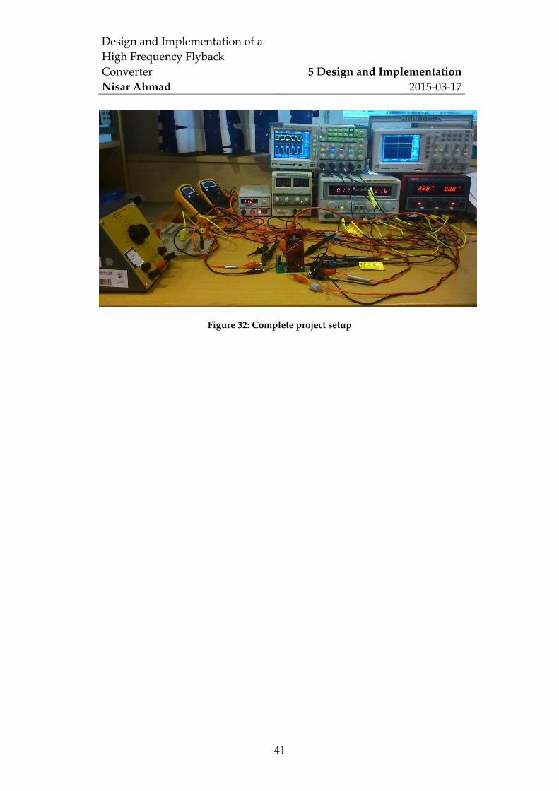
The project setup in working condition is displayed in Figure 31.
Figure 31: Measurement process of the project
Control Section
DsPIC33FJ16GS502
Switch Circuitry
Gate Driver &
CoolMos FET
PCB Planar
Transformer
&
Output Filtering
PWM
Vout
Debugging &
Programming
Environment
Design and Implementation of a
High Frequency Flyback
Converter
Nisar Ahmad
5 Design and Implementation
2015-03-17
40
The load resistances values initially selected to carry out results are 10Ω
and 15Ω. These load values are adjusted using a rheostat. Later load
resistance is increased up to 70Ω maximum with slight variance in
resistance and the results are analyzed to find the load value having
maximum efficiency. While increasing the load resistance values 22Ω is
found to have maximum efficiency and later on this value is selected for
further applications. Similarly, the duty cycle is varied to a maximum of
50%. The input voltage is gradually increased to 112V maximum with a
20%- duty cycle, as a low duty cycle allows increasing the range of input
voltage due to less switch stress. Nominal input voltage selection is
made by varying the input voltage with an increment of 5V and results
are analyzed. The maximum efficiency specifying the nominal input
voltage is 85V. By keeping the input voltage fixed at 85V, load values
are varied and nominal load value of 22Ω is selected in this process. To
increase the input supply voltage range, power supplies are connected
in series in the application. Using a dspic33f family microcontroller
PWM is initialized by using a dedicated PWM channel. To analyze the
effect of duty cycle variance, Vin and load values are kept constant for
each duty cycle value. In the process of analysis, switching frequency is
varied starting from a range of KHz to MHz. The desired results regard-
ing converter output power and efficiency are achieved in MHz fre-
quency range. While maintaining the switching frequency in MHz
range, the duty cycle value of 35% is kept constant, however, input
voltage is increased and behaviour of drain voltage is observed. Using a
CoolMOS IPL60R385CP semiconductor device, the desired quasi reso-
nant converter is implemented. The MOSFET is turned on at the lowest
drain voltage region where efficiency is observed to be maximal. The
input voltage with drain and gate voltages are continuously observed
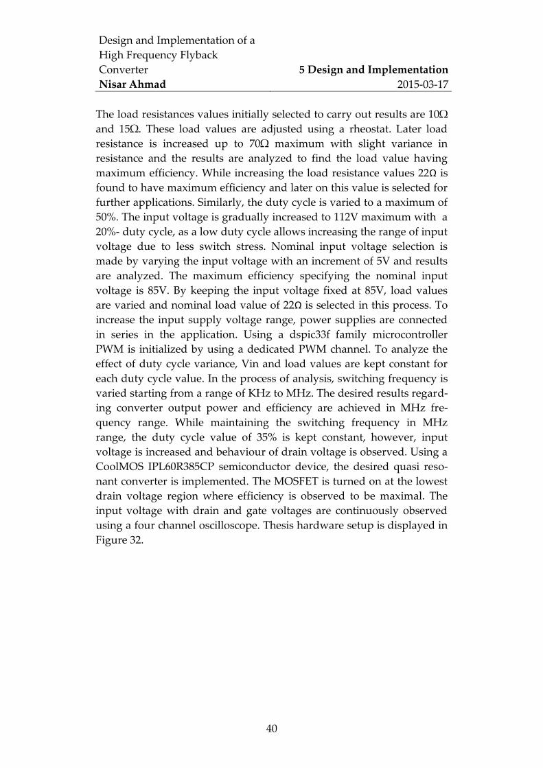
using a four channel oscilloscope. Thesis hardware setup is displayed in
Figure 32.
Design and Implementation of a
High Frequency Flyback
Converter
Nisar Ahmad
5 Design and Implementation
2015-03-17
41
Figure 32: Complete project setup
Design and Implementation of a
High Frequency Flyback
Converter
Nisar Ahmad
6 Results
2015-03-17
42
6 Results The converter is designed and analysed thoroughly. The parameters
associated to the converter are varied and respective variance in
behaviour is observed and discussed. In the following sections,
waveforms and graphs are plotted related to each parameter.
6.1 Quasi Resonant Mode
The most important factors that limit the efficiency and performance of
the converter are switching losses and thermal losses. A soft switching
technique is implemented to turn the switch ON at the lowest drain
voltage which reduces the switching losses and switch stress. Similarly,
thermal losses, generated due to hard switching, are harmful for the
device operation and are removed by adopting soft switching. All of the
results presented and discussed are taken in quasi resonant converter
mode (QRC).
6.1.1 Parameters Variance
The flyback converter parameters include input voltage (Vin), duty
cycle, switching frequency (Fsw) and load (Rl) values. To analyze the
behaviour of the converter, each parameter is varied so that others are
kept constant to observe the influence of the respective parameter on the
drain voltage (Vds), input current (Iin), output current (Iout), input
power (Pin), output power (Pout) and efficiency.
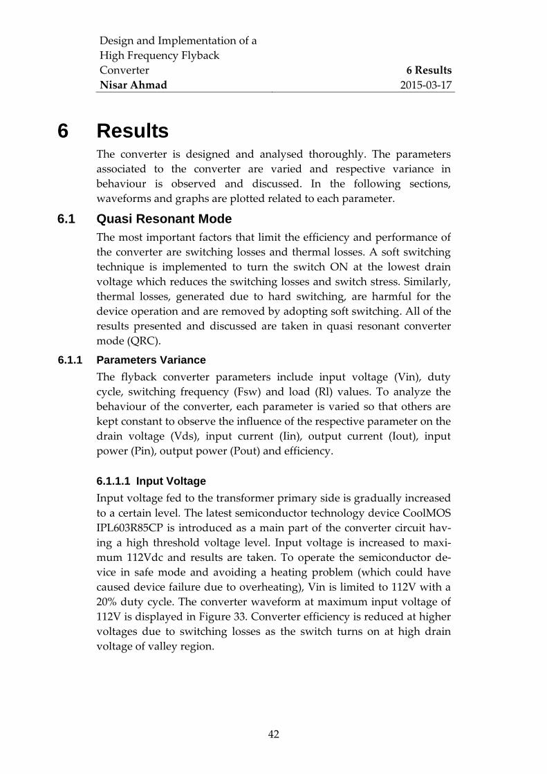
6.1.1.1 Input Voltage
Input voltage fed to the transformer primary side is gradually increased
to a certain level. The latest semiconductor technology device CoolMOS
IPL603R85CP is introduced as a main part of the converter circuit hav-
ing a high threshold voltage level. Input voltage is increased to maxi-
mum 112Vdc and results are taken. To operate the semiconductor de-
vice in safe mode and avoiding a heating problem (which could have
caused device failure due to overheating), Vin is limited to 112V with a
20% duty cycle. The converter waveform at maximum input voltage of
112V is displayed in Figure 33. Converter efficiency is reduced at higher
voltages due to switching losses as the switch turns on at high drain
voltage of valley region.
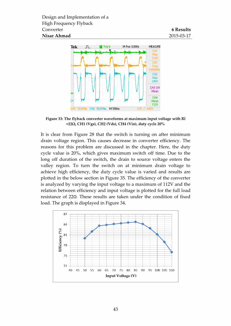
Design and Implementation of a
High Frequency Flyback
Converter
Nisar Ahmad
6 Results
2015-03-17
43
Figure 33: The flyback converter waveforms at maximum input voltage with Rl
=22Ω, CH1 (Vgs), CH2 (Vds), CH4 (Vin), duty cycle 20%
It is clear from Figure 28 that the switch is turning on after minimum
drain voltage region. This causes decrease in converter efficiency. The
reasons for this problem are discussed in the chapter. Here, the duty
cycle value is 20%, which gives maximum switch off time. Due to the
long off duration of the switch, the drain to source voltage enters the
valley region. To turn the switch on at minimum drain voltage to
achieve high efficiency, the duty cycle value is varied and results are
plotted in the below section in Figure 35. The efficiency of the converter
is analyzed by varying the input voltage to a maximum of 112V and the
relation between efficiency and input voltage is plotted for the full load
resistance of 22Ω. These results are taken under the condition of fixed
load. The graph is displayed in Figure 34.
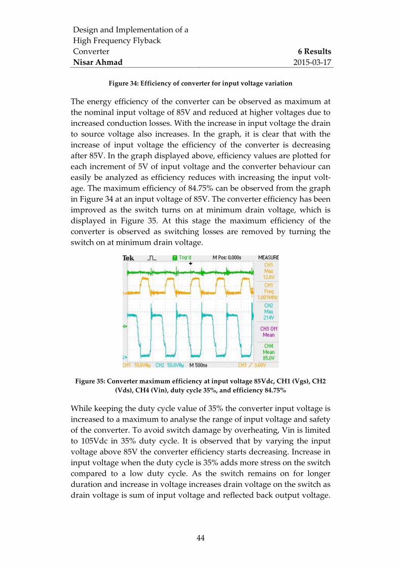
Design and Implementation of a
High Frequency Flyback
Converter
Nisar Ahmad
6 Results
2015-03-17
44
Figure 34: Efficiency of converter for input voltage variation
The energy efficiency of the converter can be observed as maximum at
the nominal input voltage of 85V and reduced at higher voltages due to
increased conduction losses. With the increase in input voltage the drain
to source voltage also increases. In the graph, it is clear that with the
increase of input voltage the efficiency of the converter is decreasing
after 85V. In the graph displayed above, efficiency values are plotted for
each increment of 5V of input voltage and the converter behaviour can
easily be analyzed as efficiency reduces with increasing the input volt-
age. The maximum efficiency of 84.75% can be observed from the graph
in Figure 34 at an input voltage of 85V. The converter efficiency has been
improved as the switch turns on at minimum drain voltage, which is
displayed in Figure 35. At this stage the maximum efficiency of the
converter is observed as switching losses are removed by turning the
switch on at minimum drain voltage.
Figure 35: Converter maximum efficiency at input voltage 85Vdc, CH1 (Vgs), CH2
(Vds), CH4 (Vin), duty cycle 35%, and efficiency 84.75%
While keeping the duty cycle value of 35% the converter input voltage is
increased to a maximum to analyse the range of input voltage and safety
of the converter. To avoid switch damage by overheating, Vin is limited
to 105Vdc in 35% duty cycle. It is observed that by varying the input
voltage above 85V the converter efficiency starts decreasing. Increase in
input voltage when the duty cycle is 35% adds more stress on the switch
compared to a low duty cycle. As the switch remains on for longer
duration and increase in voltage increases drain voltage on the switch as
drain voltage is sum of input voltage and reflected back output voltage.
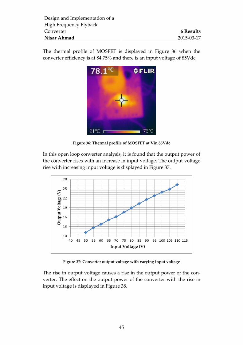
Design and Implementation of a
High Frequency Flyback
Converter
Nisar Ahmad
6 Results
2015-03-17
45
The thermal profile of MOSFET is displayed in Figure 36 when the
converter efficiency is at 84.75% and there is an input voltage of 85Vdc.
Figure 36: Thermal profile of MOSFET at Vin 85Vdc
In this open loop converter analysis, it is found that the output power of
the converter rises with an increase in input voltage. The output voltage
rise with increasing input voltage is displayed in Figure 37.
Figure 37: Converter output voltage with varying input voltage
The rise in output voltage causes a rise in the output power of the con-
verter. The effect on the output power of the converter with the rise in
input voltage is displayed in Figure 38.
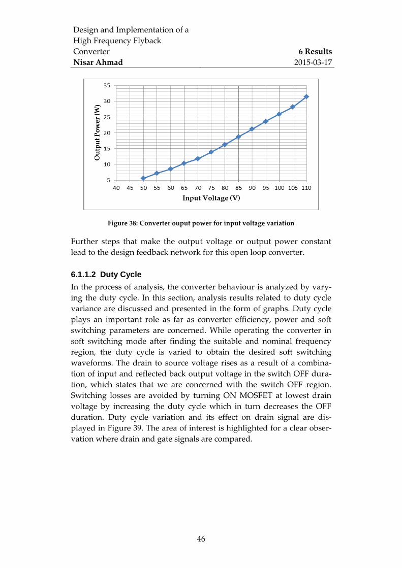
Design and Implementation of a
High Frequency Flyback
Converter
Nisar Ahmad
6 Results
2015-03-17
46
Figure 38: Converter ouput power for input voltage variation
Further steps that make the output voltage or output power constant
lead to the design feedback network for this open loop converter.
6.1.1.2 Duty Cycle
In the process of analysis, the converter behaviour is analyzed by vary-
ing the duty cycle. In this section, analysis results related to duty cycle
variance are discussed and presented in the form of graphs. Duty cycle
plays an important role as far as converter efficiency, power and soft
switching parameters are concerned. While operating the converter in
soft switching mode after finding the suitable and nominal frequency
region, the duty cycle is varied to obtain the desired soft switching
waveforms. The drain to source voltage rises as a result of a combina-
tion of input and reflected back output voltage in the switch OFF dura-
tion, which states that we are concerned with the switch OFF region.
Switching losses are avoided by turning ON MOSFET at lowest drain
voltage by increasing the duty cycle which in turn decreases the OFF
duration. Duty cycle variation and its effect on drain signal are dis-
played in Figure 39. The area of interest is highlighted for a clear obser-
vation where drain and gate signals are compared.
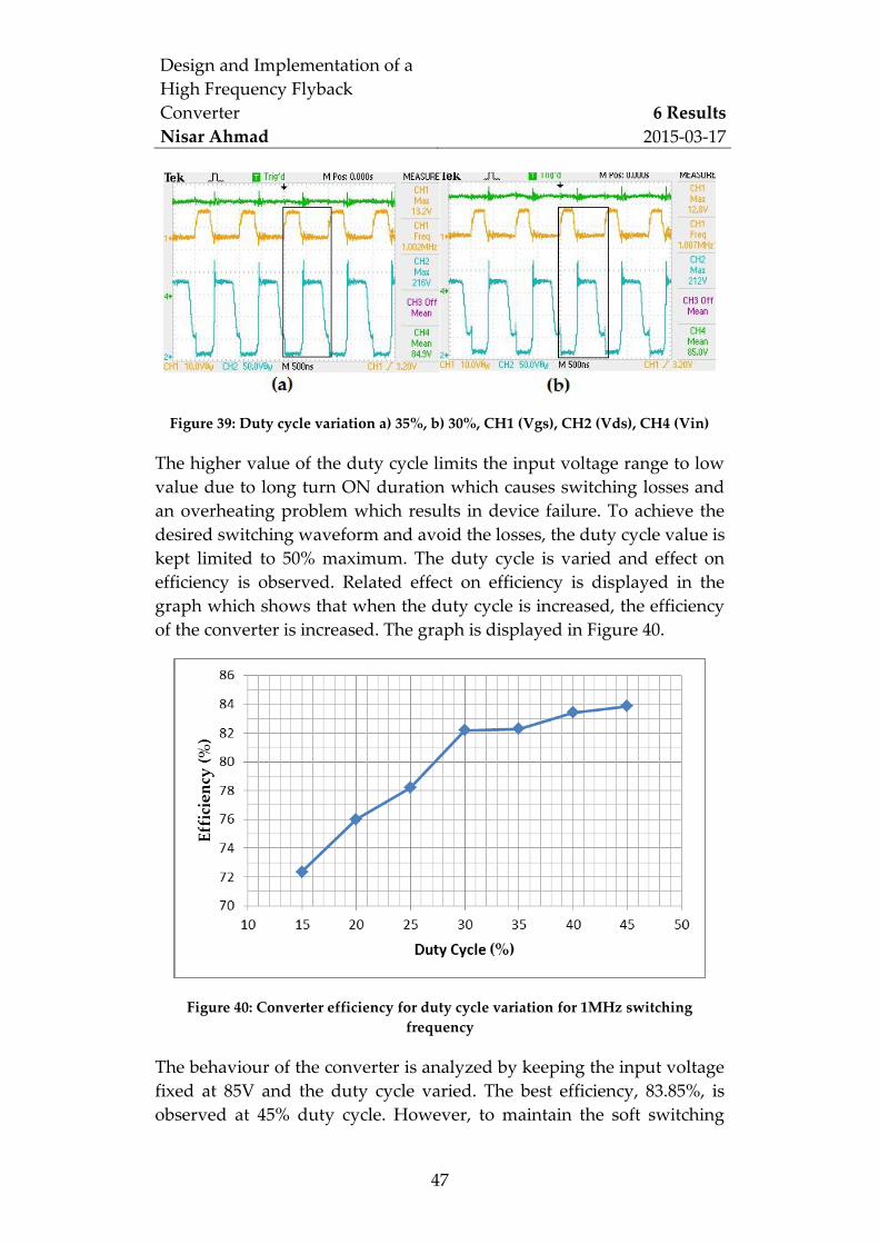
Design and Implementation of a
High Frequency Flyback
Converter
Nisar Ahmad
6 Results
2015-03-17
47
Figure 39: Duty cycle variation a) 35%, b) 30%, CH1 (Vgs), CH2 (Vds), CH4 (Vin)
The higher value of the duty cycle limits the input voltage range to low
value due to long turn ON duration which causes switching losses and
an overheating problem which results in device failure. To achieve the
desired switching waveform and avoid the losses, the duty cycle value is
kept limited to 50% maximum. The duty cycle is varied and effect on
efficiency is observed. Related effect on efficiency is displayed in the
graph which shows that when the duty cycle is increased, the efficiency
of the converter is increased. The graph is displayed in Figure 40.
Figure 40: Converter efficiency for duty cycle variation for 1MHz switching
frequency
The behaviour of the converter is analyzed by keeping the input voltage
fixed at 85V and the duty cycle varied. The best efficiency, 83.85%, is
observed at 45% duty cycle. However, to maintain the soft switching
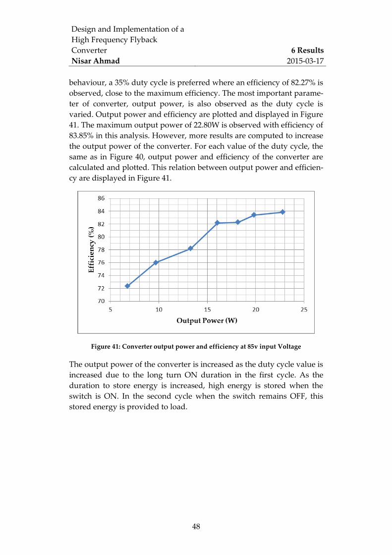
Design and Implementation of a
High Frequency Flyback
Converter
Nisar Ahmad
6 Results
2015-03-17
48
behaviour, a 35% duty cycle is preferred where an efficiency of 82.27% is
observed, close to the maximum efficiency. The most important parame-
ter of converter, output power, is also observed as the duty cycle is
varied. Output power and efficiency are plotted and displayed in Figure
41. The maximum output power of 22.80W is observed with efficiency of
83.85% in this analysis. However, more results are computed to increase
the output power of the converter. For each value of the duty cycle, the
same as in Figure 40, output power and efficiency of the converter are
calculated and plotted. This relation between output power and efficien-
cy are displayed in Figure 41.
Figure 41: Converter output power and efficiency at 85v input Voltage
The output power of the converter is increased as the duty cycle value is
increased due to the long turn ON duration in the first cycle. As the
duration to store energy is increased, high energy is stored when the
switch is ON. In the second cycle when the switch remains OFF, this
stored energy is provided to load.
Design and Implementation of a
High Frequency Flyback
Converter
Nisar Ahmad
6 Results
2015-03-17
49
6.1.1.3 Connected Load
The converter efficiency is investigated under varied load conditions,
therefore resistive load values are varied and respective effect on effi-
ciency is observed. Similarly, it is observed that to achieve high values of
output power, low resistive values are used. In the analysis, the maxi-
mum load value of 70Ω is used. Load resistance values are increased
gradually for a fixed value of input voltage of 85V, and observed effi-
ciency is plotted in Figure 42. From the graph it can be observed that
with an increase in load resistance values, efficiency decreases.
Figure 42: Converter efficiecny for load regulation
In the analysis, nominal load value is found by keeping the input
parameters fixed and varying the load resistance values. The suitable
value of load selected is 22Ω where efficiency was at its maximum of
80.83% in load analysis. In load regulation for the open loop flyback
converter load resistance, values are varied at nominal input voltage.
Design and Implementation of a
High Frequency Flyback
Converter
Nisar Ahmad
7 Discussion
2015-03-17
50
7 Discussion The aim of this research was to investigate the possibilities and methods
to implement a high frequency flyback converter with high input volt-
age and efficiency. Later, this research could lead us to adapter applica-
tion with ambitions to commercialize the product.
To explore the possibilities of high input voltages and efficiencies, the
latest technology CoolMOS power MOSFET has been introduced in this
work to replace previously implemented GaN MOSFET. A flyback
converter with GaN switch offers high efficiencies but limits the range of
input voltage to 70V maximum. However, the flyback converter with a
CoolMOS switch increased the range of input voltage to 112v with an
efficiency of approximately 76% displayed in Figure 34. In CoolMOS the
output capacitance Coss provides a high value of stored charge that
prevents from achieving good soft switching, which leads to lower
efficiencies. In this research, efforts are made to turn on switch at mini-
mum drain voltage to remove losses. Quasi resonant switching has been
achieved but complete zero voltage switching has not been achieved.
During this research factors have been investigated which limit the
converter to achieve complete zero voltage switching, which are trans-
former leakage inductance and switch output capacitance shows that the
switch is turned on at minimum drain voltage instead of zero voltage.
To achieve complete zero voltage switching, it is suggested that the
capacitor is discharged completely, which provides certain voltage
which oscillates with resonance between output capacitor and primary
inductor. Introducing an inductor across capacitor will reduce the capac-
itor voltage. The overheating of power MOSFET has been observed at
higher voltages, which limited the range of input voltage to 112V. Using
the CoolMOS power MOSFET high efficiency flyback converter can be
predicted by introducing external circuitry to discharge the output
capacitor at high input voltages.
The behaviour of the flyback converter using a 4:1 planar transformer
has been analysed in detail by introducing high breakdown voltage
CoolMOS power MOSFET. The comparison of converter behaviour with
the previously implemented converter having GaN MOSFET has been
presented above. Based on the achieved results it is concluded that this
Design and Implementation of a
High Frequency Flyback
Converter
Nisar Ahmad
7 Discussion
2015-03-17
51
research work could proceed to closed loop implementation of flyback
converter.
As far as goals and their achievement in the thesis are concerned, the
main objective was to investigate possibilities to design an open loop
high frequency flyback converter above 70V. This objective has been
achieved by reaching the maximum of 112V, but high efficiency is sacri-
ficed to operate the converter above 85V in this design. The observation
and analysis that lead to the possibilities to achieve high efficiencies at
higher voltages have been discussed above. Maximum efforts have been
done for the detailed converter analysis by using PCB planar transform-
er and their observation and analysis in connection with parameters
variance has been presented. The efficiency under different parameter
conditions such as input voltage, duty cycle and load value has been
investigated and presented in the form of graphs. However, high effi-
ciency at high voltages has not been achieved. Efforts have been made to
achieve complete soft switching behaviour, but due to the parasitics
involved, quasi resonant switching is achieved instead.
The methods and their accuracy are the key points to fulfil any task or
project on the whole. Initially, more time was spent selecting methods
and implementing them. The in implementation method desired soft
switching waveforms were achieved after facing problems related to
transformer core. The methods were made accurate after making itera-
tions increasing the time to achieve desired results.
7.1 Ethics and Impact on Society
The flyback converter design having planar PCB transformers reduces
the size of the SMPS and increases the ease of use. Using power
MOSFET having high breakdown voltage could handle more drain
voltage therefore allows an increase of the range of input voltage which
was limited to less input voltage in previous designs. Therefore, size
compactness makes it easier to carry and it takes up less space. While
working it has no harm to the surroundings. The impact on society will
be positive due to its smaller size and weight, which leads to an envi-
ronmentally friendly product, compared to the previous large-size
converters and power supplies.
Design and Implementation of a
High Frequency Flyback
Converter
Nisar Ahmad
8 Conclusion
2015-03-17
52
8 Conclusion The switching concepts that are the main subject of discussion as far as
the flyback converter design and implementation are concerned, are
discussed in detail. The basics of DC to DC converters and its types,
especially flyback as one of the most preferred SMPS topologies, have
been presented. A comparison between hard and soft switching tech-
niques is also made and benefits of soft switching related to removal of
losses are highlighted. The design characteristics of multilayer planar
PCB step-down power transformer used in the project are included.
Based on background concepts related to the flyback converter, a high
frequency flyback converter has been designed, implemented and the
results are discussed with design methodologies. The behaviour of the
converter is analysed thoroughly by varying the parameters; their effect
on efficiency and output power are presented in the form of graphs.
Similarly, soft switching results have been made possible by turning the
switch ON at lowest drain voltage in the MHz frequency region. A high
breakdown voltage semiconductor device has been introduced in this
research work to an increase in the range of input voltage. Quasi reso-
nant converter topology has been implemented and an increase in
output power and efficiency is observed. The maximum input voltage is
increased to 112V and maximum efficiency of 84.75% is observed at an
input voltage of 85V. In the load selection the value of 22Ω is selected as
the nominal value for the converter. An open loop flyback converter
application is made possible by using a 4:1 step-down multilayer PCB
transformer and a high breakdown voltage CoolMOS semiconductor
device.
8.1 Future Work
As future work the closed loop implementation of the flyback converter
can be done to regulate the output voltage to a required level that could
proceed current research into an innovative design. The heating prob-
lem in the circuit needs to be focused to increase the performance of
converter and safety of power MOSFET. The efficiency at higher voltag-
es can be increased by adopting several methods presented in the dis-
cussion.
Design and Implementation of a
High Frequency Flyback
Converter
Nisar Ahmad
References
2015-03-17
53
References
[1] Philips Semiconductors, ‚Switched Mode Power Supplies An
introduction to Switched Mode Power Supply Topologies‛ Power
Semiconductor Applications, Page 107
http://www.nxp.com/documents/application_note/APPCHP2.pdf
Retrieved 2014-04-11.
[2] Maxim Integrated, ‚An Introduction to Switched Mode Power
Supplies‛, http://www.maximintegrated.com/en/app-
notes/index.mvp/id/4087
Published 2007-09-27 Retrieved 2014-03-10
[3] Philips Semiconductors, ‛Using Power Semiconductors in
Switched Mode Power Supplies‛,
http://www.nxp.com/documents/application_note/APPCHP2.pdf
Retrieved 2014-03-10
[4] Stack Exchange Electrical Engineering, ‚Output Current of a
Boost Converter‛
http://electronics.stackexchange.com/questions/71656/what-
actually-is-the-output-current-of-a-boost-conveter
Edited 2013-06-05 Retrieved 2014-03-10
[5] Aimtron, ‚Basic Principle of Buck‛
ftp://ftp.dei.polimi.it/outgoing/Massimo.Ghioni/Power%20Electro
nics%20/DC-DC%20converters/buck/Buck%20Converter.pdf
Retrieved 2014-04-12
[6] eCircuit Center, ‚SMPS Basics the Buck Converter‛
http://www.ecircuitcenter.com/Circuits/smps_buck/smps_buck.ht
m
Retrieved 2014-04-10
Design and Implementation of a
High Frequency Flyback
Converter
Nisar Ahmad
References
2015-03-17
54
[7] EE IIT, Flyback type switched mode power supply, Module 3 DC
to DC Converters, Version 2 Lesson 22, Kharagpur
http://nptel.iitk.ac.in/courses/Webcourse-
contents/IIT%20Kharagpur/Power%20Electronics/PDF/L-
22%28DP%29%28PE%29%20%28%28EE%29NPTEL%29.pdf
Retrieved 2014-04-10
[8] Lisa Dinwoodie, ‛Isolated 50 Watt Flyback Converter using the
UCC3809 Primary Side Controller‛, Application note U-165
SLUU096, June 2001, Page 4
http://www.ti.com/lit/ug/sluu096/sluu096.pdf
Published June 2001 Retrieved 2014-04-12
[9] Tiger Zhou, ‚Primary Side Sensing Takes Complexity out of
Isolated Flyback Converter Design‛, Linear Technology, January
2009, Page 2
http://cds.linear.com/docs/en/lt-journal/LTMag-V18N4-06a-
LT3573-Tiger_Zhou.pdf
Retrieved 2014-04-15
[10] Jean Picard, ‚Under the Hood of Flyback SMPS Designs‛ Texas
Instrument power supply design seminar SEM 1900, Topic 1 TI
Literature Number SLUP261
http://www.ti.com/lit/ml/slup261/slup261.pdf
Published year 2010 Retrieved 2014-04-10
[11] Marian K. Kazimierczuk,‛ Pulse width Modulated DC-DC Power
converters‛ 2008
http://samples.sainsburysebooks.co.uk/9780470694657_sample_3790
24.pdf
Retrieved 2014-04-20
[12] Maxim Integrated, ‚An Efficiency primer for switch mode DC to
DC converter power supplies‛
http://www.maximintegrated.com/app-notes/index.mvp/id/4266
Published 2008-12-23 Retrieved 2014-04-18
Design and Implementation of a
High Frequency Flyback
Converter
Nisar Ahmad
References
2015-03-17
55
[13] Hari Babu Kotte, ‛High Speed (MHz) Switch Mode Power Sup-
plies (SMPS) using coreless PCB Transformer Technology, Thesis
for the degree of Licentiate of Technology, ISSN 1652-8948,
Sundsvall 2011
[14] Kwang Hua Liu and Fred C.Y.Lee, ‚Zero Voltage Switching
Technique in DC/DC Converters‛, IEEE Transactions on Power
Electronics, vol.5, issue 3, pp.293-304, ISSN 0885-8993, July 1990
[15] Michael T. Zhang, Milan M. Jovanovic and F.C Lee, ‚Design
Consideration and Performance Evaluations of Synchronous Rec-
tification in Flyback Converters‛, IEEE Transactions on Power
Electronics, vol.13, no.3, pp. 538-546, 1998
[16] H.B. Kotte, R. Ambatipudi and Kent Bertilsson, ‛ A ZVS Flyback
DC-DC converter using multilayer coreless printed circuit board
(PCB) step down power transformer‛, World Academy of Science
Engineering and Technology, Issue 70, ISSN 1307-6892, vol.4 no.
10, pp. 148-155, October 2010
[17] L Huber and M. M Jovanovic, ‚Evaluation of Flyback topologies
for notebook ac/dc adapter/charger applications‛, Proceedings on
High frequency Power Conversion, vol., no., pp. 284-294, May
1995
[18] Hari Babu Kotte, Radhika Ambatipudi, Kent Bertilsson, ‚High
Speed (MHz) Series Resonant Converter (SRC) Using Multilayer
Coreless Printed Circuit Board (PCB) Step-Down Power Trans-
former‛, IEEE Transactions on Power Electronics, Vol.28,no.3,
pp.1253-1264, March 2013
[19] Radhika Ambatipudi, Hari Babu Kotte and Kent Bertilsson‚High
Performance Planar Power Transformer with High Power Densi-
ty in MHz Frequency Region for Next Generation Switch Mode
Power Supplies‛ IEEE Transactions on Power Electronics, vol.,
no., pp.2139-2143, ISBN 978-1-4673-4355-8, March 2013
[20] Data sheet of dsPIC33Fj16gs502 from Microchip
http://ww1.microchip.com/downloads/en/DeviceDoc/70000318g.

Design and Implementation of a
High Frequency Flyback
Converter
Nisar Ahmad
References
2015-03-17
56
[21] Electronic Design, ‚Power Mosfet Gate Drivers‛
http://electronicdesign.com/power/power-mosfet-gate-drivers
Published 2004-07-19. Retrieved 2014-04-21.
[22] Data Sheet of LM5114 from Texas Instruments
http://www.ti.com/lit/ds/snvs790e/snvs790e.pdf
[23] Data Sheet of IPL60R385CP from Infineon Technologies
http://www.infineon.com/dgdl/IPL60R385CP_2_1.pdf?folderId=d
b3a3043163797a6011637d4bae7003b&fileId=db3a3043284aacd8012
85d06e55327e3